US20070170617A1 - Patterning Substrates Employing Multiple Chucks - Google Patents
Patterning Substrates Employing Multiple ChucksDownload PDFInfo
- Publication number
- US20070170617A1 US20070170617A1US11/625,082US62508207AUS2007170617A1US 20070170617 A1US20070170617 A1US 20070170617A1US 62508207 AUS62508207 AUS 62508207AUS 2007170617 A1US2007170617 A1US 2007170617A1
- Authority
- US
- United States
- Prior art keywords
- substrate
- chuck
- nanoimprint
- mold assembly
- substrates
- Prior art date
- Legal status (The legal status is an assumption and is not a legal conclusion. Google has not performed a legal analysis and makes no representation as to the accuracy of the status listed.)
- Granted
Links
- 239000000758substrateSubstances0.000titleclaimsabstractdescription649
- 238000000059patterningMethods0.000titleclaimsabstractdescription37
- 239000000463materialSubstances0.000claimsabstractdescription161
- 238000000034methodMethods0.000claimsabstractdescription89
- 238000001127nanoimprint lithographyMethods0.000claimsabstract5
- 239000012530fluidSubstances0.000claimsdescription51
- 238000012545processingMethods0.000claimsdescription21
- 238000000429assemblyMethods0.000claims2
- 230000000712assemblyEffects0.000claims2
- 238000004132cross linkingMethods0.000description12
- 238000012546transferMethods0.000description10
- 238000004519manufacturing processMethods0.000description9
- 230000005855radiationEffects0.000description9
- 230000033001locomotionEffects0.000description8
- 238000001459lithographyMethods0.000description7
- 238000004891communicationMethods0.000description4
- 238000010586diagramMethods0.000description4
- 239000007788liquidSubstances0.000description3
- 230000001105regulatory effectEffects0.000description3
- VYPSYNLAJGMNEJ-UHFFFAOYSA-NSilicium dioxideChemical compoundO=[Si]=OVYPSYNLAJGMNEJ-UHFFFAOYSA-N0.000description2
- 229910052734heliumInorganic materials0.000description2
- 239000001307heliumSubstances0.000description2
- SWQJXJOGLNCZEY-UHFFFAOYSA-Nhelium atomChemical compound[He]SWQJXJOGLNCZEY-UHFFFAOYSA-N0.000description2
- 238000005457optimizationMethods0.000description2
- 241000282373Panthera pardusSpecies0.000description1
- 230000015572biosynthetic processEffects0.000description1
- 239000005388borosilicate glassSubstances0.000description1
- -1but not limited toSubstances0.000description1
- 238000012937correctionMethods0.000description1
- 230000008878couplingEffects0.000description1
- 238000010168coupling processMethods0.000description1
- 238000005859coupling reactionMethods0.000description1
- 238000000151depositionMethods0.000description1
- 230000008021depositionEffects0.000description1
- 238000011161developmentMethods0.000description1
- 238000003618dip coatingMethods0.000description1
- KPUWHANPEXNPJT-UHFFFAOYSA-NdisiloxaneChemical class[SiH3]O[SiH3]KPUWHANPEXNPJT-UHFFFAOYSA-N0.000description1
- 238000005516engineering processMethods0.000description1
- 230000008020evaporationEffects0.000description1
- 238000001704evaporationMethods0.000description1
- 239000010408filmSubstances0.000description1
- 229920002313fluoropolymerPolymers0.000description1
- 239000005350fused silica glassSubstances0.000description1
- 238000005259measurementMethods0.000description1
- 239000002184metalSubstances0.000description1
- 238000012986modificationMethods0.000description1
- 230000004048modificationEffects0.000description1
- 230000003287optical effectEffects0.000description1
- 229920000620organic polymerPolymers0.000description1
- 229920000642polymerPolymers0.000description1
- 238000004886process controlMethods0.000description1
- 239000010453quartzSubstances0.000description1
- 238000002310reflectometryMethods0.000description1
- 229910052594sapphireInorganic materials0.000description1
- 239000010980sapphireSubstances0.000description1
- 229920006395saturated elastomerPolymers0.000description1
- 239000004065semiconductorSubstances0.000description1
- 238000000926separation methodMethods0.000description1
- 229910052710siliconInorganic materials0.000description1
- 239000010703siliconSubstances0.000description1
- 238000007711solidificationMethods0.000description1
- 230000008023solidificationEffects0.000description1
- 238000004528spin coatingMethods0.000description1
- 238000000427thin-film depositionMethods0.000description1
Images


Classifications
- G—PHYSICS
- G03—PHOTOGRAPHY; CINEMATOGRAPHY; ANALOGOUS TECHNIQUES USING WAVES OTHER THAN OPTICAL WAVES; ELECTROGRAPHY; HOLOGRAPHY
- G03F—PHOTOMECHANICAL PRODUCTION OF TEXTURED OR PATTERNED SURFACES, e.g. FOR PRINTING, FOR PROCESSING OF SEMICONDUCTOR DEVICES; MATERIALS THEREFOR; ORIGINALS THEREFOR; APPARATUS SPECIALLY ADAPTED THEREFOR
- G03F7/00—Photomechanical, e.g. photolithographic, production of textured or patterned surfaces, e.g. printing surfaces; Materials therefor, e.g. comprising photoresists; Apparatus specially adapted therefor
- G03F7/0002—Lithographic processes using patterning methods other than those involving the exposure to radiation, e.g. by stamping
- B—PERFORMING OPERATIONS; TRANSPORTING
- B29—WORKING OF PLASTICS; WORKING OF SUBSTANCES IN A PLASTIC STATE IN GENERAL
- B29C—SHAPING OR JOINING OF PLASTICS; SHAPING OF MATERIAL IN A PLASTIC STATE, NOT OTHERWISE PROVIDED FOR; AFTER-TREATMENT OF THE SHAPED PRODUCTS, e.g. REPAIRING
- B29C59/00—Surface shaping of articles, e.g. embossing; Apparatus therefor
- B29C59/02—Surface shaping of articles, e.g. embossing; Apparatus therefor by mechanical means, e.g. pressing
- B29C59/022—Surface shaping of articles, e.g. embossing; Apparatus therefor by mechanical means, e.g. pressing characterised by the disposition or the configuration, e.g. dimensions, of the embossments or the shaping tools therefor
- B—PERFORMING OPERATIONS; TRANSPORTING
- B82—NANOTECHNOLOGY
- B82Y—SPECIFIC USES OR APPLICATIONS OF NANOSTRUCTURES; MEASUREMENT OR ANALYSIS OF NANOSTRUCTURES; MANUFACTURE OR TREATMENT OF NANOSTRUCTURES
- B82Y10/00—Nanotechnology for information processing, storage or transmission, e.g. quantum computing or single electron logic
- B—PERFORMING OPERATIONS; TRANSPORTING
- B82—NANOTECHNOLOGY
- B82Y—SPECIFIC USES OR APPLICATIONS OF NANOSTRUCTURES; MEASUREMENT OR ANALYSIS OF NANOSTRUCTURES; MANUFACTURE OR TREATMENT OF NANOSTRUCTURES
- B82Y40/00—Manufacture or treatment of nanostructures
- H—ELECTRICITY
- H01—ELECTRIC ELEMENTS
- H01L—SEMICONDUCTOR DEVICES NOT COVERED BY CLASS H10
- H01L21/00—Processes or apparatus adapted for the manufacture or treatment of semiconductor or solid state devices or of parts thereof
- H01L21/67—Apparatus specially adapted for handling semiconductor or electric solid state devices during manufacture or treatment thereof; Apparatus specially adapted for handling wafers during manufacture or treatment of semiconductor or electric solid state devices or components ; Apparatus not specifically provided for elsewhere
- H01L21/683—Apparatus specially adapted for handling semiconductor or electric solid state devices during manufacture or treatment thereof; Apparatus specially adapted for handling wafers during manufacture or treatment of semiconductor or electric solid state devices or components ; Apparatus not specifically provided for elsewhere for supporting or gripping
- H01L21/687—Apparatus specially adapted for handling semiconductor or electric solid state devices during manufacture or treatment thereof; Apparatus specially adapted for handling wafers during manufacture or treatment of semiconductor or electric solid state devices or components ; Apparatus not specifically provided for elsewhere for supporting or gripping using mechanical means, e.g. chucks, clamps or pinches
- Y—GENERAL TAGGING OF NEW TECHNOLOGICAL DEVELOPMENTS; GENERAL TAGGING OF CROSS-SECTIONAL TECHNOLOGIES SPANNING OVER SEVERAL SECTIONS OF THE IPC; TECHNICAL SUBJECTS COVERED BY FORMER USPC CROSS-REFERENCE ART COLLECTIONS [XRACs] AND DIGESTS
- Y10—TECHNICAL SUBJECTS COVERED BY FORMER USPC
- Y10S—TECHNICAL SUBJECTS COVERED BY FORMER USPC CROSS-REFERENCE ART COLLECTIONS [XRACs] AND DIGESTS
- Y10S977/00—Nanotechnology
- Y10S977/84—Manufacture, treatment, or detection of nanostructure
- Y10S977/887—Nanoimprint lithography, i.e. nanostamp
Definitions
- Nano-fabricationinvolves the fabrication of very small structures, e.g., having features on the order of nanometers or smaller.
- One area in which nano-fabrication has had a sizeable impactis in the processing of integrated circuits.
- nano-fabricationbecomes increasingly important. Nano-fabrication provides greater process control while allowing increased reduction of the minimum feature dimension of the structures formed.
- Other areas of development in which nano-fabrication has been employedinclude biotechnology, optical technology, mechanical systems and the like.
- An exemplary nano-fabrication techniqueis commonly referred to as imprint lithography.
- Exemplary imprint lithography processesare described in detail in numerous publications, such as U.S. patent application publication 2004/0065976 filed as U.S. patent application Ser. No. 10/264,960, entitled, “Method and a Mold to Arrange Features on a Substrate to Replicate Features having Minimal Dimensional Variability”; U.S. patent application publication 2004/0065252 filed as U.S. patent application Ser. No. 10/264,926, entitled “Method of Forming a Layer on a Substrate to Facilitate Fabrication of Metrology Standards”; and U.S. Pat. No. 6,936,194, entitled “Functional Patterning Material for Imprint Lithography Processes,” all of which are assigned to the assignee of the present invention.
- the imprint lithography technique disclosed in each of the aforementioned United States patent application publications and United States patentincludes formation of a relief pattern in a polymerizable layer and transferring a pattern corresponding to the relief pattern into an underlying substrate.
- the substratemay be positioned upon a motion stage to obtain a desired position to facilitate patterning thereof.
- a templateis employed spaced-apart from the substrate with a formable liquid present between the template and the substrate.
- the liquidis solidified to form a solidified layer that has a pattern recorded therein that is conforming to a shape of the surface of the template in contact with the liquid.
- the templateis then separated from the solidified layer such that the template and the substrate are spaced-apart.
- the substrate and the solidified layerare then subjected to processes to transfer, into the substrate, a relief image that corresponds to the pattern in the solidified layer.
- FIG. 1is a simplified side view of a lithographic system having a mold spaced-apart from a substrate in accordance with the prior art
- FIG. 2is a top down view of a robot handling the substrate shown in FIG. 1 ;
- FIG. 3is a flow diagram showing a method of patterning the substrate shown in FIG. 1 ;
- FIG. 4is a simplified side view of a lithographic system having a mold spaced-apart from first and second substrates positioned on first and second substrate chucks, respectively;
- FIG. 5is a flow diagram showing a method of patterning the first and second substrate shown in FIG. 4 ;
- FIG. 6is a simplified side view of the lithographic system shown in FIG. 4 , with the robot positioning the first substrate on the first substrate chuck;
- FIG. 7is a simplified side view of the lithographic system shown in FIG. 6 , with the first substrate having a material positioned thereon;
- FIG. 8is a simplified side view of the lithographic system shown in FIG. 7 , with the mold contacting the material positioned on the first substrate and the robot positioning the second substrate on the second substrate chuck;
- FIG. 9is a simplified side view of the lithographic system shown in FIG. 8 , with the mold being separated from the material on the first substrate;
- FIG. 10is a simplified side view of the lithographic system shown in FIG. 9 , with the second substrate having a material positioned thereon;
- FIG. 11is a simplified side view of the lithographic system shown in FIG. 10 , with the mold contacting the material positioned on the second substrate and the robot removing the first substrate from the first substrate chuck;
- FIG. 12is a simplified side view of the lithographic system shown in FIG. 11 , with the mold being separated from the material on the second substrate and a third substrate positioned on the first substrate chuck;
- FIG. 13is a simplified side view of the lithographic system shown in FIG. 12 , with the third substrate having a material positioned thereon;
- FIG. 14is a simplified side view of the lithographic system shown in FIG. 13 , with the mold contacting the material positioned on the third substrate and the robot removing the second substrate from the second substrate chuck;
- FIG. 15is a flow diagram showing a method of patterning first and second sides of the first and second substrates shown in FIG. 4 ;
- FIG. 16is a simplified side diagram of the lithographic system shown in FIG. 10 , with the mold contacting the material positioned on the second substrate and the robot flipping the first substrate with respect to the mold;
- FIG. 17is a simplified side view of the lithographic system shown in FIG. 16 , with the mold being separated from the material on the second substrate and the first substrate positioned on the first substrate chuck in a second position;
- FIG. 18is a simplified side view of the lithographic system shown in FIG. 17 , with the first substrate having a material positioned thereon;
- FIG. 19is a simplified side view of the lithographic system shown in FIG. 18 , with the mold contacting the material positioned on the first substrate and the robot flipping the second substrate with respect to the mold;
- FIG. 20is a simplified side view of the lithographic system shown in FIG. 19 , with the mold being separated from the material on the first substrate and the second substrate positioned on the second substrate chuck in a second position;
- FIG. 21is a simplified side view of the lithographic system shown in FIG. 20 , with the second substrate having a material positioned thereon;
- FIG. 22is a simplified side view of the lithographic system shown in FIG. 21 , with the mold contacting the material positioned on the second substrate and the robot removing the first substrate from the first substrate chuck;
- FIG. 23is a simplified side view of the lithographic system shown in FIG. 22 , with the mold being separated from the material on the second substrate and a third substrate positioned on the first substrate chuck;
- FIG. 24is a simplified side view of the lithographic system shown in FIG. 23 , with the third substrate having a material positioned thereon;
- FIG. 25is a simplified side view of the lithographic system shown in FIG. 24 with the mold contacting the material positioned on the third substrate and the robot removing the second substrate from the second substrate chuck;
- FIG. 26is a simplified top down view of the lithographic system shown in FIG. 4 , with the lithographic system have first and second modules each comprising first and second substrate chucks, with the first substrates being patterned;
- FIG. 27is a simplified top down view of the lithographic system shown in FIG. 4 , with the lithographic system have first and second modules each comprising first and second substrate chucks, with the second substrates being patterned;
- FIG. 28is a simplified side view of a substrate chuck having a substrate positioned thereon;
- FIG. 29is an exploded view of a portion of the substrate shown in FIG. 4 ;
- FIG. 30is an exploded view of a portion of the substrate chuck shown in FIG. 4 .
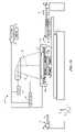
- First substrate 12 amay be coupled to a first substrate chuck 14 a .
- First substrate chuck 12 amay be any chuck including, but not limited to, vacuum, pin-type, groove type, or electromagnetic, as described in U.S. Pat. No. 6,873,087 entitled “High-Precision Orientation Alignment and Gap Control Stages for Imprint Lithography Processes” which is incorporated herein by reference.
- First substrate chuck 14 amay comprise a cavity 16 a facing first substrate 12 a .
- First substrate 12 a and first substrate chuck 14 amay be supported on a first stage 18 and a second stage 20 , with first stage 18 being positioned between first substrate chuck 14 a and second stage 20 . Further, first and second stages 18 and 20 may be positioned on a base 22 . First stage 18 may provide motion about a first axis while second stage 20 may provide motion about a second axis, the second axis being orthogonal to the first axis, i.e. the first and second axes being the x and y axes. Exemplary stages in the present invention are available under part numbers XM200L350 and XM200S50, both from Newport Corporation of Irvine, Calif. First substrate 12 a may further comprise a throughway 24 a . However, in a further embodiment, first substrate 12 a may be substantially absent of throughway 24 a.
- a template 26Spaced-apart from first substrate 12 a is a template 26 having a mesa 28 extending therefrom towards first substrate 12 a with a patterning surface 30 thereon.
- Mesa 28may also be referred to as a mold 28 .
- Mesa 28may also be referred to as a nanoimprint mold 28 .
- template 26may be substantially absent of mold 28 .
- Template 26 and/or mold 28may be formed from such material including but not limited to, fused-silica, quartz, silicon, organic polymers, siloxane polymers, borosilicate glass, fluorocarbon polymers, metal, and hardened sapphire.
- patterning surface 30comprises features defined by a plurality of spaced-apart recesses 32 and protrusions 34 .
- patterning surface 30may be substantially smooth and/or planar. Patterning surface 30 may define an original pattern that forms the basis of a pattern to be formed on first substrate 12 a , described further below.
- Template 26may be coupled to a template chuck 36 , template chuck 36 being any chuck including, but not limited to, vacuum, pin-type, groove type, or electromagnetic, as described in U.S. Pat. No. 6,873,087 entitled “High-Precision Orientation Alignment and Gap Control Stages for Imprint Lithography Processes”.
- template chuck 36may be coupled to an imprint head 38 to facilitate movement of template 26 and mold 28 .
- imprint head 38may be a three degree-of-freedom (two tilting motions and one translational motion) stage controlled by a three-voice coil actuators (not shown) or other linear actuators (not shown).
- System 10further comprises a first fluid dispenser 40 a .
- First fluid dispenser 40 amay be in fluid communication with first substrate 12 a so as to position a polymeric material 42 a thereon, described further below.
- first fluid dispenser 40 ais coupled to template chuck 36 ; however, in a further embodiment, first fluid dispenser 40 a may be coupled to any part of system 10 , i.e., template 26 or imprint head 38 .
- system 10may comprise any number of fluid dispensers and first fluid dispenser 40 a may comprise a plurality of dispensing units therein. Exemplary fluid dispensers in the present invention are available under the part name Leopard from Xaar Corporation located in Cambridge, United Kingdom.
- Polymeric material 42 amay be positioned upon first substrate 12 a using any known technique, e.g., drop dispense, spin-coating, dip coating, thin film deposition, thick film deposition, and the like. As shown, polymeric material 42 a may be positioned upon first substrate 12 a as a plurality of spaced-apart droplets 44 a . In an example, each droplet of droplets 44 a may have a unit volume of approximately 6 pico-liters. Typically, polymeric material 42 a may be positioned upon first substrate 12 a before the desired volume is defined between mold 28 and first substrate 12 a , described further below. However, polymeric material 42 a may fill the volume after the desired volume has been obtained.
- drop dispensespin-coating
- dip coatingthin film deposition
- thick film depositionthick film deposition
- polymeric material 42 amay be positioned upon first substrate 12 a using any known technique, e.g., drop dispense, spin-coating, dip coating, thin film deposition,
- System 10further comprises a source 46 of energy 48 to direct energy 48 along a path 50 .
- Imprint head 38 and first and second stages 18 and 20are configured to arrange mold 28 and first substrate 12 a , respectively, to be in superimposition and disposed within path 50 , described further below.
- Either imprint head 38 , first and second stages 18 and 20 , or a combination of the above,may vary a distance between mold 28 and first substrate 12 a to define a desired volume therebetween that is filled by polymeric material 42 a .
- source 46may be a He lamp or He/Xe lamp or LED based source that may emit UV in the range of 300 to 380 nm.
- system 10further comprises a robot 52 for positioning first substrate 12 a upon and removing first substrate 12 a from first substrate chuck 14 a .
- Robot 52may be any handling robot known in the art.
- robot 52comprises an arm 54 coupled to a driving means 56 .
- Arm 54further has an end effecter 58 coupled thereto to handle first substrate 12 a .
- end effecter 58may be an edge-gripping or thin air cavity chuck to hold substrate 12 a without contacting an area of first substrate 12 a having polymeric material 42 a positioned thereon, respectively, i.e., the active area of substrate 12 a .
- Driving means 56many extend or contract arm 54 , move arm 54 horizontally in a circle, or provide any desired motion of arm 54 .
- Driving means 56may also provide motion about the first and second axes mentioned above.
- Driving means 56may also rotate about its axis, i.e., about a joint 59 .
- Arm 54may also rotate about an axis 55 to flip first substrate 12 a 180° with respect to mold 28 , described further below. Further, arm 54 may rotate about a joint 57 .
- robot 52may transport first substrate 12 a between first substrate chuck 14 a and a substrate cassette (not shown).
- the substrate cassette (not shown)may comprise a plurality of substrates therein.
- system 10may be regulated by a processor 58 that is in data communication with first and second stages 18 and 20 , imprint head 38 , first fluid dispenser 40 a , source 46 , and robot 52 , operating on a computer readable program stored in memory 60 .
- first substrate 12 amay be positioned upon first substrate chuck 14 a . More specifically, first and second stages 18 and 20 may position first substrate chuck 14 a in a desired spatial relationship with respect to robot 52 such that robot 52 may position first substrate 12 a upon first substrate chuck 14 a . Robot 52 may transfer first substrate 12 a from the substrate cassette (not shown) and position the same upon first substrate chuck 14 a . At step 72 , first and second stages 18 and 20 may translate first substrate 12 a such that a desired position may be obtained between first substrate 12 a and first fluid dispenser 40 a . As a result, first fluid dispenser 40 a may position polymeric material 42 a upon first substrate 12 a , as mentioned above. Polymeric material 42 a may be a nanoimprint material.
- first and second stages 18 and 20 and imprint head 38may position first substrate chuck 14 a such that first substrate 12 a may be in superimposition with mold 28 and further polymeric material 42 a fills the desired volume between first substrate 12 a and mold 28 .
- the atmosphere between mold 28 and droplets 44 amay be saturated with helium or is completely evacuated or is a partially evacuated atmosphere of helium.
- source 46may produce energy 48 , e.g., broadband ultraviolet radiation that causes first polymeric material 42 a to solidify and/or cross-link conforming to a shape of first substrate 12 a and patterning surface 30 of mold 28 .
- energy 48e.g., broadband ultraviolet radiation that causes first polymeric material 42 a to solidify and/or cross-link conforming to a shape of first substrate 12 a and patterning surface 30 of mold 28 .
- mold 28may be separated from polymeric material 42 a positioned on first substrate 12 a .
- first substrate 12 amay be unloaded from first substrate chuck 14 a . More specifically, first and second stages 18 and 20 may position first substrate 12 a in a desired spatial relationship to robot 52 such that robot 52 may remove first substrate 12 a from first substrate chuck 14 a and position the same within the substrate cassette (not shown).
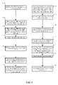
- the aforementioned process for patterning first substrate 12 amay have a total process time per substrate of thirty-four (34) seconds. More specifically, the time for each step of the aforementioned patterning process is shown more clearly in Chart 1:
- the steps for the aforementioned method of processing first substrate 12 amay be performed sequentially.
- a portion of system 10may not be operating at full capacity, i.e., a portion of system 10 may remain idle with respect to the remaining portions of system 10 .
- the steps of 1) positioning first substrate 12 a on first substrate chuck 14 acomprise a majority of the process time to process first substrate 12 a .
- imprint head 38 and/or template 26 and/or mold 28 and/or robot 52may be not be operating at full capacity, i.e., remain idle for periods of time, which may be undesirable.
- an optimization of the aforementioned method of patterning a substratemay be desired, and more specifically, an optimization of steps 1 , 3 , and 5 may be desired.
- steps 1 , 3 , and 5may be desired.
- a total increase in throughput of processing multiple substratesand similarly, a decrease in total process time per substrate
- described beloware a system and a method of processing multiple substrates concurrently.
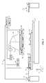
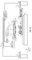
- a system 10 ′is shown.
- System 10 ′may be analogous to that as system 10 described above with respect to FIG. 1 , however, system 10 ′ may comprise a second substrate 12 b coupled to a second substrate chuck 14 b .
- Second substrate 12 b and second substrate chuck 14 bmay be analogous to that of first substrate 12 a and first substrate chuck 14 a , respectively, as described above with respect to FIG. 1 .
- Second substrate chuck 14 bmay comprise a cavity 16 b facing second substrate 12 b .
- Second substrate 12 b and second substrate chuck 14 bmay be supported on first and second stages 18 and 20 .
- Second substrate 12 bmay further comprise a throughway 24 b .
- second substrate 12 bmay be substantially absent of throughway 24 b.
- System 10 ′further comprises a second fluid dispenser 40 b , analogous to that of first fluid dispenser 40 a .
- second fluid dispenser 40 bis coupled to template chuck 36 ; however, in a further embodiment, second fluid dispenser 40 b may be coupled to any part of system 10 , i.e. template 24 or imprint head 38 .
- Control of second fluid dispenser 40 bmay be regulated by processor 58 that is in communication with second fluid dispenser 40 b .
- robot 52is shown as two separate bodies and coupling between processor 58 and first and second stages 18 and 20 is not shown.
- first substrate 12 amay be positioned upon first substrate chuck 14 a . More specifically, first and second stages 18 and 20 may position first substrate chuck 14 a in a desired spatial relationship with respect to robot 52 such that robot 52 may position first substrate 12 a upon first substrate chuck 14 a . Robot 52 may transfer first substrate 12 a from the substrate cassette (not shown) and position the same upon first substrate chuck 14 a.
- first and second stages 18 and 20may translate first substrate chuck 14 a such that a desired position may be obtained between first substrate 12 a and first fluid dispenser 40 a to position polymeric material 42 a on first substrate 12 a.
- a desired spatial relationshipmay be obtained between first substrate 12 a and mold 28 . More specifically, first and second stages 18 and 20 and imprint head 38 may position first substrate chuck 14 a such that first substrate 12 a may be in superimposition with mold 28 and further polymeric material 42 a fills the desired volume between first substrate 12 a and mold 28 . Further, at step 104 , after the desired volume is filled with polymeric material 42 a , source 46 may produce energy 48 , e.g., broadband ultraviolet radiation that causes polymeric material 42 a to solidify and/or cross-link conforming to a shape of first substrate 12 a and patterning surface 30 of mold 28 .
- energy 48e.g., broadband ultraviolet radiation that causes polymeric material 42 a to solidify and/or cross-link conforming to a shape of first substrate 12 a and patterning surface 30 of mold 28 .
- processing of second substrate 12 bmay occur concurrently with processing of first substrate 12 a . More specifically, at step 106 , concurrently with step 104 , robot 52 may transfer second substrate 12 b from the substrate cassette (not shown) and position the same upon second substrate chuck 14 b.
- step 108mold 28 may be separated from polymeric material 42 a positioned on first substrate 12 a .
- step 108may occur concurrently with step 104 and step 106 .
- first and second stages 18 and 20may translate second substrate chuck 14 b such that a desired position may be obtained between second substrate 12 b and second fluid dispenser 40 b to position polymeric material 42 b on second substrate 12 b .
- polymeric material 42 bmay be positioned upon second substrate 12 b as a plurality of spaced-apart droplets 44 b.
- a desired spatial relationshipmay be obtained between second substrate 12 b and mold 28 . More specifically, first and second stages 18 and 20 and imprint head 38 may position second substrate chuck 14 b such that second substrate 12 b may be in superimposition with mold 28 and further polymeric material 42 b fills the desired volume between second substrate 12 b and mold 28 . Further, at step 112 , after the desired volume is filled with polymeric material 42 b , source 46 may produce energy 48 , e.g., broadband ultraviolet radiation that causes polymeric material 42 b to solidify and/or cross-link conforming to a shape of second substrate 12 b and patterning surface 30 of mold 28 .
- energy 48e.g., broadband ultraviolet radiation that causes polymeric material 42 b to solidify and/or cross-link conforming to a shape of second substrate 12 b and patterning surface 30 of mold 28 .
- robot 52may remove first substrate 12 a from first substrate chuck 14 a and position the same within the substrate cassette (not shown) and further robot 52 may position a third substrate 12 c , shown in FIG. 12 , upon first substrate chuck 14 a .
- Robot 52may transfer third substrate 12 c , shown in FIG. 12 , from the substrate cassette (not shown) and position the same upon first substrate chuck 14 a.
- mold 28may be separated from polymeric material 42 b positioned on second substrate 12 b .
- step 116may occur concurrently with step 112 and step 114 .
- first and second stages 18 and 20may translate third substrate 12 c such that a desired position may be obtained between third substrate 12 c and first fluid dispenser 40 a to position polymeric material 42 c on third substrate 12 c .
- polymeric material 42 cmay be positioned upon third substrate 12 c as a plurality of spaced-apart droplets 44 c.
- a desired spatial relationshipmay be obtained between third substrate 12 c and mold 28 . More specifically, first and second stages 18 and 20 and imprint head 38 may position first substrate chuck 14 a such that third substrate 12 c may be in superimposition with mold 28 and further polymeric material 42 c fills the desired volume between third substrate 12 c and mold 28 . Further, at step 120 , after the desired volume is filled with polymeric material 42 c , source 46 may produce energy 48 , e.g., broadband ultraviolet radiation that causes polymeric material 42 c to solidify and/or cross-link conforming to a shape of third substrate 12 c and patterning surface 30 of mold 28 .
- energy 48e.g., broadband ultraviolet radiation that causes polymeric material 42 c to solidify and/or cross-link conforming to a shape of third substrate 12 c and patterning surface 30 of mold 28 .
- robot 52may remove second substrate 12 b from second substrate chuck 14 b and position the same within the substrate cassette (not shown) and further robot 52 may position a fourth substrate (not shown) upon second substrate chuck 14 b .
- Robot 52may transfer the fourth substrate (not shown) from the substrate cassette (not shown) and position the same upon second substrate chuck 14 b .
- Third substrate 12 c and the fourth substrate (not shown), both analogous to that of first substrate 12 amay be subjected to the aforementioned processing conditions, analogous to that of first and second substrates 12 a and 12 b.
- an additional substratemay be patterned on second substrate chuck 14 b prior to patterning of second substrate 12 b .
- the additional substrate(not shown), previously positioned on second substrate chuck 14 b and having a polymeric material (not shown) positioned thereon, may have a pattern formed thereon analogous to that of step 112 shown in FIG. 11 .
- mold 28may be separated form the polymeric material (not shown) positioned on the additional substrate (not shown), analogous to that of step 116 shown in FIG. 12 .
- step 106may further include removing the additional substrate (not shown), analogous to that of step 122 shown in FIG. 14 .
- step 100may also further include removing a second additional substrate (not shown), previously patterned and positioned on first substrate chuck 14 a prior to first substrate 12 a , analogous to that of step 114 shown in FIG. 11 .
- first and second fluid dispensers 40 a and 40 bmay be positioned outside of system 110 , with first and second substrates 12 a and 12 b having polymeric material 42 a and 42 b , respectively, positioned thereon outside of system 110 .
- positioning of polymeric material 42 a and 42 b upon first and second substrate 12 a and 12 bmay be optional.
- the aforementioned patterning process for first and second substrates 12 a and 12 bmay have a total process time per substrate of twenty (20) seconds. More specifically, the time for each step of the aforementioned patterning process is shown more clearly in Chart 2:
- the steps for the aforementioned method of processing first and second substrates 12 a and 12 bmay be performed in parallel. More specifically, the steps of 1) positioning a substrate upon or removing a substrate from a substrate chuck and 2) obtaining a desired spatial relationship between the substrate and a mold with polymeric material filling a desired volume between the substrate and the mold and solidifying and/or cross-linking the polymeric material or separating the mold from the polymeric material occurs in parallel. As a result, a total increase in throughput of processing multiple substrates (and similarly, a decrease in total process time per substrate) may be obtained, which may be desirable.
- first and second stages 18 and 20may rotate about a third axis extending orthogonal to first and second stages 18 , i.e. the z axis, and may rotate for more than 180°.
- the aforementioned methodmay be employed to form a pattern on first sides 62 a and 62 b of first and second substrates 12 a and 12 b , respectively.
- itmay be desired to form a pattern on second sides 64 a and 64 b of first and second substrates 12 a and 12 b , respectively, with second sides 64 a and 64 b being positioned opposite to that of first and second sides 62 a and 62 b , respectively.
- first substrate 12may be positioned upon first substrate chuck 14 a . More specifically, first and second stages 18 and 20 may position first substrate chuck 14 a in a desired spatial relationship with respect to robot 52 such that robot 52 may position first substrate 12 a upon first substrate chuck 14 a . Robot 52 may transfer first substrate 12 a from the substrate cassette (not shown) and position the same upon first substrate chuck 14 a such that first side 62 a may be positioned opposite to that of first substrate chuck 14 a.
- first and second stages 18 and 20may translate first substrate 12 a such that a desired position may be obtained between first substrate 12 a and first fluid dispenser 40 a to position polymeric material 42 a on first side 62 a of first substrate 12 a.
- a desired spatial relationshipmay be obtained between first substrate 12 a and mold 28 . More specifically, first and second stages 18 and 20 and imprint head 38 may position first substrate chuck 14 a such that first substrate 12 a may be in superimposition with mold 28 and further polymeric material 42 a fills the desired volume between first substrate 12 a and mold 28 . Further, at step 104 , after the desired volume is filled with polymeric material 42 a , source 46 may produce energy 48 , e.g., broadband ultraviolet radiation that causes polymeric material 42 a to solidify and/or cross-link conforming to a shape of first side 62 a of first substrate 12 a and patterning surface 30 of mold 28 .
- energy 48e.g., broadband ultraviolet radiation that causes polymeric material 42 a to solidify and/or cross-link conforming to a shape of first side 62 a of first substrate 12 a and patterning surface 30 of mold 28 .
- processing of second substrate 12 bmay occur concurrently with processing of first substrate 12 a . More specifically, at step 206 , concurrently with step 204 , robot 52 may transfer second substrate 12 b from the substrate cassette (not shown) and position the same upon second substrate chuck 14 b such that first side 62 b may be positioned opposite to that of second substrate chuck 14 b.
- step 207mold 28 may be separated from polymeric material 42 a positioned on first side 62 a of first substrate 12 a .
- step 207may occur concurrently with step 204 and step 206 .
- first and second stages 18 and 20may translate second substrate 12 b such that a desired position may be obtained between second substrate 12 b and second fluid dispenser 40 b to position polymeric material 42 b on first side 62 b of second substrate 12 b .
- polymeric material 42 bmay be positioned upon second substrate 12 b as a plurality of spaced-apart droplets 44 b.
- a desired spatial relationshipmay be obtained between second substrate 12 b and mold 28 . More specifically, first and second stages 18 and 20 and imprint head 38 may position second substrate chuck 14 b such that second substrate 12 b may be in superimposition with mold 28 and further polymeric material 42 b fills the desired volume between second substrate 12 b and mold 28 . Further, at step 210 , after the desired volume is filled with polymeric material 42 b , source 46 may produce energy 48 , e.g., broadband ultraviolet radiation that causes polymeric material 42 b to solidify and/or cross-link conforming to a shape of first side 62 b of second substrate 12 b and patterning surface 30 of mold 28 .
- energy 48e.g., broadband ultraviolet radiation that causes polymeric material 42 b to solidify and/or cross-link conforming to a shape of first side 62 b of second substrate 12 b and patterning surface 30 of mold 28 .
- robot 52may remove first substrate 12 a from first substrate chuck 14 a and rotate arm 54 around its axis to flip first substrate 12 a 180° with respect to mold 28 and further robot 52 may position first substrate 12 a upon first substrate chuck 14 a such that second side 64 a may be positioned opposite to that of first substrate chuck 14 a , as shown in FIG. 17 .
- polymeric material 42 amay be positioned within cavity 16 a of first substrate chuck 14 a to minimize, if not prevent, damage to polymeric material 42 a.
- step 216mold 28 may be separated from polymeric material 42 b positioned on second substrate 12 b .
- step 216may occur concurrently with step 210 and step 212 .
- first and second stages 18 and 20may translate first substrate 12 a such that a desired position may be obtained between first substrate 12 a and first fluid dispenser 40 a to position polymeric material 42 a ′ on first substrate 12 a .
- polymeric material 42 a ′may be positioned upon first substrate 12 a as a plurality of spaced-apart droplets 44 a′.
- a desired spatial relationshipmay be obtained between first substrate 12 a and mold 28 . More specifically, first and second stages 18 and 20 and imprint head 38 may position first substrate chuck 14 a such that first substrate 12 a may be in superimposition with mold 28 and further polymeric material 42 a ′ fills the desired volume between first substrate 12 a and mold 28 . Further, at step 220 , after the desired volume is filled with polymeric material 42 a ′, source 46 may produce energy 48 , e.g., broadband ultraviolet radiation that causes polymeric material 42 a ′ to solidify and/or cross-link conforming to a shape of second surface 64 a of first substrate 12 a and patterning surface 30 of mold 28 .
- energy 48e.g., broadband ultraviolet radiation that causes polymeric material 42 a ′ to solidify and/or cross-link conforming to a shape of second surface 64 a of first substrate 12 a and patterning surface 30 of mold 28 .
- robot 52may remove first substrate 12 a from first substrate chuck 14 a and rotate arm 54 around its axis to flip second substrate 12 b 180° with respect to mold 28 and further robot 52 may position second substrate 12 b upon second substrate chuck 14 b such that second side 64 b may be positioned opposite to that of second substrate chuck 14 b , as shown in FIG. 20 .
- polymeric material 42 bmay be positioned within cavity 16 b of second substrate chuck 14 b to minimize, if not prevent, damage to polymeric material 42 b.
- mold 28may be separated from polymeric material 42 a ′ positioned on second side 64 a of first substrate 12 a .
- step 224may occur concurrently with step 220 and step 222 .
- first and second stages 18 and 20may translate second substrate chuck 14 b such that a desired position may be obtained between second substrate 12 b and second fluid dispenser 40 b to position polymeric material 42 b ′ on second side 64 b of second substrate 12 b .
- polymeric material 42 b ′may be positioned upon second substrate 12 b as a plurality of spaced-apart droplets 44 b′.
- a desired spatial relationshipmay be obtained between second substrate 12 b and mold 28 . More specifically, first and second stages 18 and 20 and imprint head 38 may position second substrate chuck 14 b such that second substrate 12 b may be in superimposition with mold 28 and further polymeric material 42 b ′ fills the desired volume between second substrate 12 b and mold 28 . Further, at step 228 , after the desired volume is filled with polymeric material 42 b ′, source 46 may produce energy 48 , e.g., broadband ultraviolet radiation that causes polymeric material 42 b ′ to solidify and/or cross-link conforming to a shape of second side 64 b of second substrate 12 b and patterning surface 30 of mold 28 .
- energy 48e.g., broadband ultraviolet radiation that causes polymeric material 42 b ′ to solidify and/or cross-link conforming to a shape of second side 64 b of second substrate 12 b and patterning surface 30 of mold 28 .
- robot 52may remove first substrate 12 a from first substrate chuck 14 a and position the same within the substrate cassette (not shown) and further robot 52 may position a third substrate 12 c upon first substrate chuck 14 a .
- Robot 52may transfer third substrate 12 c from the substrate cassette (not shown) and position the same upon first substrate chuck 14 a such that first side 62 c may be positioned opposite to that of first substrate chuck 14 a.
- mold 28may be separated from polymeric material 42 b ′ positioned on second substrate 12 b .
- step 232may occur concurrently with step 228 and step 230 .
- first and second stages 18 and 20may translate third substrate 12 c such that a desired position may be obtained between third substrate 12 c and first fluid dispensers 40 a to position polymeric material 42 c on third substrate 12 c .
- polymeric material 42 cmay be positioned upon third substrate 12 c as a plurality of spaced-apart droplets 44 c.
- a desired spatial relationshipmay be obtained between third substrate 12 c and mold 28 . More specifically, first and second stages 18 and 20 and imprint head 38 may position first substrate chuck 14 a such that third substrate 12 c may be in superimposition with mold 28 and further polymeric material 42 c fills the desired volume between third substrate 12 c and mold 28 . Further, at step 236 , after the desired volume is filled with polymeric material 42 c , source 46 may produce energy 48 , e.g., broadband ultraviolet radiation that causes polymeric material 42 c to solidify and/or cross-link conforming to a shape of first surface 62 c of third substrate 12 c and patterning surface 30 of mold 28 .
- energy 48e.g., broadband ultraviolet radiation that causes polymeric material 42 c to solidify and/or cross-link conforming to a shape of first surface 62 c of third substrate 12 c and patterning surface 30 of mold 28 .
- robot 52may remove second substrate 12 b from second substrate chuck 14 b and position the same within the substrate cassette (not shown) and further robot 52 may position an additional substrate (not shown) upon second substrate chuck 14 b .
- Robot 52may transfer the additional substrate (not shown) from the substrate cassette (not shown) and position the same upon second substrate chuck 14 b .
- Third substrate 12 c and the additional substratemay be subjected to the aforementioned processing conditions, analogous to that of first and second substrates 12 a and 12 b.
- an additional substratemay be patterned on second substrate chuck 14 b prior to patterning of second substrate 12 b .
- the additional substrate(not shown), previously positioned on second substrate chuck 14 b and having a polymeric material (not shown) positioned thereon, may have a pattern formed on a second side thereon analogous to that of step 228 shown in FIG. 22 .
- mold 28may be separated form the polymeric material (not shown) positioned on the additional substrate (not shown), analogous to that of step 232 shown in FIG. 23 .
- step 206may further include removing the additional substrate (not shown), analogous to that of step 238 shown in FIG. 25 .
- step 200may also further include removing a second additional substrate (not shown), previously patterned and positioned on first substrate chuck 13 a prior to first substrate 12 a , analogous to that of step 230 , shown in FIG. 22 .
- the aforementioned process for patterning first and second sides 62 a and 64 a of first substrate 12 a and first and second sides 62 b and 64 b of second substrate 12 bmay have a total process time per substrate of forty (40) seconds. More specifically, the time for each step of the aforementioned patterning process is shown more clearly in Chart 3:
- the steps for the aforementioned method of processing first and second sides 62 a and 64 a of first substrate 12 a and first and second sides 62 b and 64 b of second substrate 12 bmay be performed in parallel. More specifically, analogous to that mentioned above with respect Chart 2, the steps of 1) positioning a substrate upon or removing a substrate from a substrate chuck and 2) obtaining a desired spatial relationship between the substrate and a mold with polymeric material filling a desired volume between the substrate and the mold and solidifying and/or cross-linking the polymeric material or separating the mold from the polymeric material occurs in parallel. As a result, a total increase in throughput of processing multiple substrates (and similarly, a decrease in total process time per substrate) may be obtained, which may be desirable.
- the above-mentioned processesmay be employed in imprint lithography systems including, inter alia, a step-and-repeat system and a whole wafer system.
- the selection of the systemis known to one skilled in the art and typically depends on the specific application which is desired.
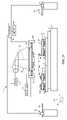
- system 110may comprise any number of substrate chucks.
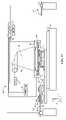
- system 110may comprise a first and a second module 66 a and 66 b .
- First module 66 amay comprise first and second substrate chucks 14 a and 14 b and second module 66 b may comprise third and fourth substrate chucks 14 c and 14 d .
- Third and fourth substrate chucks 14 c and 14 dmay be analogous to that of first and second substrate chucks 14 a and 14 b , respectively, mentioned above with respect to FIG. 4 .
- third and fourth substrate chucks 14 c and 14 dmay have third and fourth substrates 12 c and 12 d positioned thereon, analogous to first and second substrate 12 a and 12 b mentioned above with respect to FIG. 4 , and may be submitted to substantially the same processing conditions as mentioned above with respect to FIG. 15 . More specifically, processing of first and second modules 66 a and 66 b may be occur in parallel, i.e., each module of first and second modules 66 a and 66 b may be subjected to the process as mentioned above with respect to FIG. 15 , concurrently.
- a substrate of first and second substrates 12 a and 12 b of first module 66 a and a substrate of third and fourth substrates 12 c and 12 d of second module 66 bmay be patterned while concurrently the remaining substrate of first and second substrates 12 a and 12 b of first module 66 a and the remaining substrate of third and fourth substrates 12 c and 12 d of second module 66 b may be in the input/output process. More specifically, first substrate 12 a may be patterned as analogous to that of steps 204 and 206 mentioned above with respect to FIGS. 8 and 15 and third substrate 12 c may be patterned as analogous to that of steps 222 and 226 mentioned above with respect to FIGS. 15 and 22 .
- second substrate 12 bmay be positioned upon second substrate chuck 14 b as analogous to that of step 206 mentioned above with respect to FIGS. 8 and 15 and fourth substrate 12 d may be removed (or removed and flipped) from fourth substrate chuck 14 d analogous to that of step 230 mentioned above with respect to FIGS. 15 and 25 (or analogous to that of step 222 mentioned above with respect to FIGS. 15 and 19 ).
- template 26is shown as a dashed rectangle.
- second substrate 12 bmay be patterned as analogous to that of steps 204 and 206 mentioned above with respect to FIGS. 8 and 15 and fourth substrate 12 d may be patterned as analogous to that of step 226 mentioned above with respect to FIGS. 15 and 22 .
- first substrate 12 amay be positioned upon first substrate chuck 14 a as analogous to that of step 206 mentioned above with respect to FIGS. 8 and 15 and third substrate 12 c may be removed (or removed and flipped) from third substrate chuck 14 c analogous to that of step 230 mentioned above with respect to FIGS. 15 and 25 (or analogous to that of step 222 mentioned above with respect to FIGS. 15 and 19 ).
- a substrate having a patterned formed on first and second sides thereofmay be formed every n seconds, with n seconds being the time to pattern a side of the substrate.
- First substrate chuck 14 amay comprise a plurality of lands 68 positioned around an active area 80 of first substrate 12 a .
- First substrate chuck 14 amay further comprises a throughway 82 that may be in fluid communication with a pump system 84 to facilitate obtaining a desired pressure within cavity 16 a .
- Control of pump system 84may be regulated by processor 58 .
- first and second substrates 12 a and 12 bmay be subject to substantially the same process conditions.
- FIG. 29a portion 86 of first substrate 12 a , shown in FIG. 4 , is depicted, wherein portion 86 displays a level of planarity of first side 62 a of first substrate 12 a .
- First side 62 acomprises a plurality of hills and valleys; however, only hill 88 and valley 90 are shown.
- the plurality of hills and valleys of first side 62 adefine an average plane of planarity, shown as plane ‘a,’ of first side 62 a .
- first side 62 amay deviate from plane ‘a’ by differing magnitudes and wherein, for simplicity, each deviation may be defined as ⁇ dev1 . More specifically, a zenith of hill 88 may deviate from plane ‘a’ a magnitude ⁇ 1 and a nadir of valley 90 may deviate from plane ‘a’ a magnitude ⁇ 2 .
- the abovemay be equally applied to second side 64 a of first substrate 12 a as well as first and second sides 62 b and 64 b of second substrate 12 b . Referring to FIG. 30 , a portion 92 of first substrate chuck 14 a , shown in FIG.
- portion 92displays a level of planarity of a surface 94 of first substrate chuck 14 a .
- Surface 94comprises a plurality of hills and valleys; however, only hill 96 and valley 98 are shown.
- the plurality of hills and valleys of surface 94define an average plane of planarity, shown as plane ‘b,’ of surface 94 .
- the plurality of hills and valleys of surface 94may deviate from plane ‘b’ by differing magnitudes and wherein, for simplicity, each deviation may be defined as ⁇ dev2 .
- a zenith of hill 96may deviate from plane ‘b’ a magnitude ⁇ 3 and a nadir of valley 98 may deviate from plane ‘b’ a magnitude ⁇ 4 .
- the abovemay be equally applied to second substrate chuck 12 b .
- ⁇ dev2the deviation in thickness of surface 94 of substrate chuck 14 b may be less than ⁇ dev1 , the deviation in thickness of first side 62 a (or second side 64 a ) of first substrate 12 a .
- first and second fluid dispensers 40 a and 40 bmay be calibrated with respect to each other such that first and second substrates 12 a and 12 b may be subjected to substantially the same process conditions. More specifically, first fluid dispenser 40 a may be instructed by processor 58 to position a volume V 1 of polymeric material 42 a upon first substrate 12 a ; however, first fluid dispenser 40 a may position a volume V 2 of polymeric material 42 a upon first substrate 12 a , with volume V 2 differing from volume V 1 and volume V 1 being the desired volume. This may result from a miscalibration of first fluid dispenser 40 a , i.e. dispensing a different volume of fluid than instructed to.
- the difference between volumes V 1 and V 2may be calculated such that processor 58 , operating on computer readable program stored in memory 60 , may instruct first fluid dispenser 40 a to position a volume V 3 upon first substrate 12 a to compensate for the miscalibration such that first fluid dispenser 40 a may position volume V 1 upon first substrate 12 a .
- the abovemay be equally applied to second fluid dispenser 40 b .
- subjecting first and second substrates 12 a and 12 b to substantially the same process conditionsmay be facilitated.
- polymeric material 42 a and 42 b , positioned on first and second substrates 12 a and 12 b , respectively,may be subjected to differing evaporation conditions as a result of being positioned on differing substrate chucks, and thus, a volume of polymeric material 42 a and 42 b may differ, which is undesirable. More specifically, an air flow and temperature of an environment associated with polymeric material 42 a , first substrate 12 a , and first substrate chuck 14 a may differ that an environment associated with polymeric material 42 b , second substrate 42 b , and second substrate chuck 14 b .
- first fluid dispenser 40 amay position a volume V 4 of polymeric material 42 a upon first substrate 12 a and second fluid dispenser 40 b may positioned a volume V 5 , differing from volume V 4 , of polymeric material 42 b upon second substrate 12 b to compensate for the aforementioned evaporative conditions such that after exposure of polymeric material 42 a and 42 b to the evaporative conditions, polymeric material 42 a and 42 b comprises a volume V 6 and V 7 , respectively, with volumes V 6 and V 7 being substantially the same.
- first and second fluid dispensers 40 a and 40 b with respect to first and second substrates 12 a and 12 b , respectively,may be substantially the same to facilitate subjecting first and second substrates 12 a and 12 b to substantially the same process conditions. More specifically, a distance between first fluid dispenser 40 a and first substrate 12 a may be substantially the same as a distance between second fluid dispenser 40 b and second substrate 40 b.
- a reflectivity of surface 94 of first and second substrate chucks 14 a and 14 bmay be substantially the same such that the solidification and/or cross-linking of first and second materials 42 a and 42 b may be substantially the same.
Landscapes
- Engineering & Computer Science (AREA)
- Chemical & Material Sciences (AREA)
- Nanotechnology (AREA)
- Physics & Mathematics (AREA)
- General Physics & Mathematics (AREA)
- Crystallography & Structural Chemistry (AREA)
- Condensed Matter Physics & Semiconductors (AREA)
- Manufacturing & Machinery (AREA)
- Mathematical Physics (AREA)
- Theoretical Computer Science (AREA)
- Computer Hardware Design (AREA)
- Microelectronics & Electronic Packaging (AREA)
- Power Engineering (AREA)
- Mechanical Engineering (AREA)
- Shaping Of Tube Ends By Bending Or Straightening (AREA)
- Exposure Of Semiconductors, Excluding Electron Or Ion Beam Exposure (AREA)
- Manufacturing Of Magnetic Record Carriers (AREA)
Abstract
Description
- The present application claims priority to U.S. Provisional Application No. 60/760,738, filed on Jan. 20, 2006, entitled “Apparatus for and Methods for Nano-Imprinting with Multi-Substrate Chucks” and U.S. Provisional Application No. 60/827,125, filed on Sep. 27, 2006, entitled “Apparatus and Method for Nano-Imprinting with Multi-Substrate Chucks” and U.S. Provisional Application No. 60/788,808, filed on Apr. 3, 2006, entitled “Residual Layer Thickness Measurement and Correction”; and is a Continuation-in-Part of U.S. patent application Ser. No. 11/565,350, filed on Nov. 30, 2006, entitled “Method and System for Double-Sided Patterning of Substrates” which claims priority to U.S. Provisional Application No. 60/748,430, filed on Dec. 8, 2005, entitled “Apparatus For and Methods For Imprinting, Aligning and Separation for Double Side Imprinting”, all of which are incorporated herein by reference.
- Nano-fabrication involves the fabrication of very small structures, e.g., having features on the order of nanometers or smaller. One area in which nano-fabrication has had a sizeable impact is in the processing of integrated circuits. As the semiconductor processing industry continues to strive for larger production yields while increasing the circuits per unit area formed on a substrate, nano-fabrication becomes increasingly important. Nano-fabrication provides greater process control while allowing increased reduction of the minimum feature dimension of the structures formed. Other areas of development in which nano-fabrication has been employed include biotechnology, optical technology, mechanical systems and the like.
- An exemplary nano-fabrication technique is commonly referred to as imprint lithography. Exemplary imprint lithography processes are described in detail in numerous publications, such as U.S. patent application publication 2004/0065976 filed as U.S. patent application Ser. No. 10/264,960, entitled, “Method and a Mold to Arrange Features on a Substrate to Replicate Features having Minimal Dimensional Variability”; U.S. patent application publication 2004/0065252 filed as U.S. patent application Ser. No. 10/264,926, entitled “Method of Forming a Layer on a Substrate to Facilitate Fabrication of Metrology Standards”; and U.S. Pat. No. 6,936,194, entitled “Functional Patterning Material for Imprint Lithography Processes,” all of which are assigned to the assignee of the present invention.
- The imprint lithography technique disclosed in each of the aforementioned United States patent application publications and United States patent includes formation of a relief pattern in a polymerizable layer and transferring a pattern corresponding to the relief pattern into an underlying substrate. The substrate may be positioned upon a motion stage to obtain a desired position to facilitate patterning thereof. To that end, a template is employed spaced-apart from the substrate with a formable liquid present between the template and the substrate. The liquid is solidified to form a solidified layer that has a pattern recorded therein that is conforming to a shape of the surface of the template in contact with the liquid. The template is then separated from the solidified layer such that the template and the substrate are spaced-apart. The substrate and the solidified layer are then subjected to processes to transfer, into the substrate, a relief image that corresponds to the pattern in the solidified layer.
FIG. 1 is a simplified side view of a lithographic system having a mold spaced-apart from a substrate in accordance with the prior art;FIG. 2 is a top down view of a robot handling the substrate shown inFIG. 1 ;FIG. 3 is a flow diagram showing a method of patterning the substrate shown inFIG. 1 ;FIG. 4 is a simplified side view of a lithographic system having a mold spaced-apart from first and second substrates positioned on first and second substrate chucks, respectively;FIG. 5 is a flow diagram showing a method of patterning the first and second substrate shown inFIG. 4 ;FIG. 6 is a simplified side view of the lithographic system shown inFIG. 4 , with the robot positioning the first substrate on the first substrate chuck;FIG. 7 is a simplified side view of the lithographic system shown inFIG. 6 , with the first substrate having a material positioned thereon;FIG. 8 is a simplified side view of the lithographic system shown inFIG. 7 , with the mold contacting the material positioned on the first substrate and the robot positioning the second substrate on the second substrate chuck;FIG. 9 is a simplified side view of the lithographic system shown inFIG. 8 , with the mold being separated from the material on the first substrate;FIG. 10 is a simplified side view of the lithographic system shown inFIG. 9 , with the second substrate having a material positioned thereon;FIG. 11 is a simplified side view of the lithographic system shown inFIG. 10 , with the mold contacting the material positioned on the second substrate and the robot removing the first substrate from the first substrate chuck;FIG. 12 is a simplified side view of the lithographic system shown inFIG. 11 , with the mold being separated from the material on the second substrate and a third substrate positioned on the first substrate chuck;FIG. 13 is a simplified side view of the lithographic system shown inFIG. 12 , with the third substrate having a material positioned thereon;FIG. 14 is a simplified side view of the lithographic system shown inFIG. 13 , with the mold contacting the material positioned on the third substrate and the robot removing the second substrate from the second substrate chuck;FIG. 15 is a flow diagram showing a method of patterning first and second sides of the first and second substrates shown inFIG. 4 ;FIG. 16 is a simplified side diagram of the lithographic system shown inFIG. 10 , with the mold contacting the material positioned on the second substrate and the robot flipping the first substrate with respect to the mold;FIG. 17 is a simplified side view of the lithographic system shown inFIG. 16 , with the mold being separated from the material on the second substrate and the first substrate positioned on the first substrate chuck in a second position;FIG. 18 is a simplified side view of the lithographic system shown inFIG. 17 , with the first substrate having a material positioned thereon;FIG. 19 is a simplified side view of the lithographic system shown inFIG. 18 , with the mold contacting the material positioned on the first substrate and the robot flipping the second substrate with respect to the mold;FIG. 20 is a simplified side view of the lithographic system shown inFIG. 19 , with the mold being separated from the material on the first substrate and the second substrate positioned on the second substrate chuck in a second position;FIG. 21 is a simplified side view of the lithographic system shown inFIG. 20 , with the second substrate having a material positioned thereon;FIG. 22 is a simplified side view of the lithographic system shown inFIG. 21 , with the mold contacting the material positioned on the second substrate and the robot removing the first substrate from the first substrate chuck;FIG. 23 is a simplified side view of the lithographic system shown inFIG. 22 , with the mold being separated from the material on the second substrate and a third substrate positioned on the first substrate chuck;FIG. 24 is a simplified side view of the lithographic system shown inFIG. 23 , with the third substrate having a material positioned thereon;FIG. 25 is a simplified side view of the lithographic system shown inFIG. 24 with the mold contacting the material positioned on the third substrate and the robot removing the second substrate from the second substrate chuck;FIG. 26 is a simplified top down view of the lithographic system shown inFIG. 4 , with the lithographic system have first and second modules each comprising first and second substrate chucks, with the first substrates being patterned;FIG. 27 is a simplified top down view of the lithographic system shown inFIG. 4 , with the lithographic system have first and second modules each comprising first and second substrate chucks, with the second substrates being patterned;FIG. 28 is a simplified side view of a substrate chuck having a substrate positioned thereon;FIG. 29 is an exploded view of a portion of the substrate shown inFIG. 4 ; andFIG. 30 is an exploded view of a portion of the substrate chuck shown inFIG. 4 .- Referring to
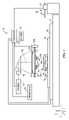
FIG. 1 , asystem 10 is shown to form a relief pattern on afirst substrate 12a.First substrate 12amay be coupled to afirst substrate chuck 14a.First substrate chuck 12amay be any chuck including, but not limited to, vacuum, pin-type, groove type, or electromagnetic, as described in U.S. Pat. No. 6,873,087 entitled “High-Precision Orientation Alignment and Gap Control Stages for Imprint Lithography Processes” which is incorporated herein by reference.First substrate chuck 14amay comprise acavity 16afacingfirst substrate 12a.First substrate 12aandfirst substrate chuck 14amay be supported on afirst stage 18 and asecond stage 20, withfirst stage 18 being positioned betweenfirst substrate chuck 14aandsecond stage 20. Further, first andsecond stages base 22.First stage 18 may provide motion about a first axis whilesecond stage 20 may provide motion about a second axis, the second axis being orthogonal to the first axis, i.e. the first and second axes being the x and y axes. Exemplary stages in the present invention are available under part numbers XM200L350 and XM200S50, both from Newport Corporation of Irvine, Calif.First substrate 12amay further comprise athroughway 24a. However, in a further embodiment,first substrate 12amay be substantially absent ofthroughway 24a. - Spaced-apart from
first substrate 12ais atemplate 26 having amesa 28 extending therefrom towardsfirst substrate 12awith apatterning surface 30 thereon. Mesa28 may also be referred to as amold 28.Mesa 28 may also be referred to as ananoimprint mold 28. In a further embodiment,template 26 may be substantially absent ofmold 28.Template 26 and/ormold 28 may be formed from such material including but not limited to, fused-silica, quartz, silicon, organic polymers, siloxane polymers, borosilicate glass, fluorocarbon polymers, metal, and hardened sapphire. As shown patterningsurface 30 comprises features defined by a plurality of spaced-apart recesses32 andprotrusions 34. However, in a further embodiment, patterningsurface 30 may be substantially smooth and/or planar. Patterningsurface 30 may define an original pattern that forms the basis of a pattern to be formed onfirst substrate 12a, described further below.Template 26 may be coupled to atemplate chuck 36,template chuck 36 being any chuck including, but not limited to, vacuum, pin-type, groove type, or electromagnetic, as described in U.S. Pat. No. 6,873,087 entitled “High-Precision Orientation Alignment and Gap Control Stages for Imprint Lithography Processes”. Further,template chuck 36 may be coupled to animprint head 38 to facilitate movement oftemplate 26 andmold 28. In an example,imprint head 38 may be a three degree-of-freedom (two tilting motions and one translational motion) stage controlled by a three-voice coil actuators (not shown) or other linear actuators (not shown). System 10 further comprises afirst fluid dispenser 40a.First fluid dispenser 40amay be in fluid communication withfirst substrate 12aso as to position apolymeric material 42athereon, described further below. As shownfirst fluid dispenser 40ais coupled totemplate chuck 36; however, in a further embodiment,first fluid dispenser 40amay be coupled to any part ofsystem 10, i.e.,template 26 orimprint head 38. Further,system 10 may comprise any number of fluid dispensers andfirst fluid dispenser 40amay comprise a plurality of dispensing units therein. Exemplary fluid dispensers in the present invention are available under the part name Leopard from Xaar Corporation located in Cambridge, United Kingdom.Polymeric material 42amay be positioned uponfirst substrate 12ausing any known technique, e.g., drop dispense, spin-coating, dip coating, thin film deposition, thick film deposition, and the like. As shown,polymeric material 42amay be positioned uponfirst substrate 12aas a plurality of spaced-apartdroplets 44a. In an example, each droplet ofdroplets 44amay have a unit volume of approximately 6 pico-liters. Typically,polymeric material 42amay be positioned uponfirst substrate 12abefore the desired volume is defined betweenmold 28 andfirst substrate 12a, described further below. However,polymeric material 42amay fill the volume after the desired volume has been obtained.System 10 further comprises asource 46 ofenergy 48 to directenergy 48 along apath 50.Imprint head 38 and first andsecond stages mold 28 andfirst substrate 12a, respectively, to be in superimposition and disposed withinpath 50, described further below. Eitherimprint head 38, first andsecond stages mold 28 andfirst substrate 12ato define a desired volume therebetween that is filled bypolymeric material 42a. In an example,source 46 may be a He lamp or He/Xe lamp or LED based source that may emit UV in the range of 300 to 380 nm.- Referring to
FIGS. 1 and 2 ,system 10 further comprises arobot 52 for positioningfirst substrate 12aupon and removingfirst substrate 12afromfirst substrate chuck 14a.Robot 52 may be any handling robot known in the art. In an example,robot 52 comprises anarm 54 coupled to a driving means56.Arm 54 further has anend effecter 58 coupled thereto to handlefirst substrate 12a. In an example, endeffecter 58 may be an edge-gripping or thin air cavity chuck to holdsubstrate 12awithout contacting an area offirst substrate 12ahavingpolymeric material 42apositioned thereon, respectively, i.e., the active area ofsubstrate 12a. Driving means56 many extend orcontract arm 54, movearm 54 horizontally in a circle, or provide any desired motion ofarm 54. Driving means56 may also provide motion about the first and second axes mentioned above. Driving means56 may also rotate about its axis, i.e., about a joint59.Arm 54 may also rotate about anaxis 55 to flipfirst substrate 12a180° with respect tomold 28, described further below. Further,arm 54 may rotate about a joint57. Furthermore,robot 52 may transportfirst substrate 12abetweenfirst substrate chuck 14aand a substrate cassette (not shown). The substrate cassette (not shown) may comprise a plurality of substrates therein. - Referring to
FIG. 1 ,system 10 may be regulated by aprocessor 58 that is in data communication with first andsecond stages imprint head 38,first fluid dispenser 40a,source 46, androbot 52, operating on a computer readable program stored inmemory 60. - Referring to
FIGS. 1 and 3 , in accordance with the prior art, a process flow for processingfirst substrate 12ais shown. Atstep 70,first substrate 12amay be positioned uponfirst substrate chuck 14a. More specifically, first andsecond stages first substrate chuck 14ain a desired spatial relationship with respect torobot 52 such thatrobot 52 may positionfirst substrate 12auponfirst substrate chuck 14a.Robot 52 may transferfirst substrate 12afrom the substrate cassette (not shown) and position the same uponfirst substrate chuck 14a. Atstep 72, first andsecond stages first substrate 12asuch that a desired position may be obtained betweenfirst substrate 12aandfirst fluid dispenser 40a. As a result,first fluid dispenser 40amay positionpolymeric material 42auponfirst substrate 12a, as mentioned above.Polymeric material 42amay be a nanoimprint material. - At
step 74, a desired spatial relationship may be obtained betweenfirst substrate 12aandmold 28. More specifically, first andsecond stages imprint head 38 may positionfirst substrate chuck 14asuch thatfirst substrate 12amay be in superimposition withmold 28 and furtherpolymeric material 42afills the desired volume betweenfirst substrate 12aandmold 28. To facilitate filling ofrecessions 32, before contact betweenmold 28 anddroplets 44a, the atmosphere betweenmold 28 anddroplets 44amay be saturated with helium or is completely evacuated or is a partially evacuated atmosphere of helium. Further, atstep 74, after the desired volume is filled withpolymeric material 42a,source 46 may produceenergy 48, e.g., broadband ultraviolet radiation that causes firstpolymeric material 42ato solidify and/or cross-link conforming to a shape offirst substrate 12aandpatterning surface 30 ofmold 28. - At
step 76,mold 28 may be separated frompolymeric material 42apositioned onfirst substrate 12a. Atstep 78,first substrate 12amay be unloaded fromfirst substrate chuck 14a. More specifically, first andsecond stages first substrate 12ain a desired spatial relationship torobot 52 such thatrobot 52 may removefirst substrate 12afromfirst substrate chuck 14aand position the same within the substrate cassette (not shown). - To that end, in an example, the aforementioned process for patterning
first substrate 12amay have a total process time per substrate of thirty-four (34) seconds. More specifically, the time for each step of the aforementioned patterning process is shown more clearly in Chart 1: CHART 1Process time Process for patterning a substrate (secs) 1 Position first substrate 12a onfirst substrate chuck 14a7 2 Obtain a desired spatial relationship between first substrate 1 12a and first fluid dispenser 40a to positionpolymeric material 42a on first substrate 12a3 Obtain a desired spatial relationship between first substrate 18 12a and mold 28 withpolymeric material 42a filling adesired volume between first substrate 12a andmold 28 andsolidifying and/or cross-linking polymeric material 42a4 Separate mold 28 frompolymeric material 42a1 5 Remove first substrate 12a fromfirst substrate chuck 14a7 Total/ Substrate 34 - To that end, the steps for the aforementioned method of processing
first substrate 12amay be performed sequentially. As a result, a portion ofsystem 10 may not be operating at full capacity, i.e., a portion ofsystem 10 may remain idle with respect to the remaining portions ofsystem 10. More specifically, the steps of 1) positioningfirst substrate 12aonfirst substrate chuck 14a(step1); 2) obtaining a desired spatial relationship betweenfirst substrate 12aandmold 28 withpolymeric material 42afilling a desired volume betweenfirst substrate 12aandmold 28 and solidifying and/or cross-linkingpolymeric material 42a(step3); and 3) removingfirst substrate 12afromfirst substrate chuck 14a(step5) comprise a majority of the process time to processfirst substrate 12a. As a result, inter alia,imprint head 38 and/ortemplate 26 and/ormold 28 and/orrobot 52 may be not be operating at full capacity, i.e., remain idle for periods of time, which may be undesirable. To that end, to maximize an efficiency ofsystem 10, an optimization of the aforementioned method of patterning a substrate may be desired, and more specifically, an optimization ofsteps 1,3, and5 may be desired. As a result, a total increase in throughput of processing multiple substrates (and similarly, a decrease in total process time per substrate) may be obtained, which may be desirable. To that end, described below are a system and a method of processing multiple substrates concurrently. - Referring to
FIG. 4 , in a first embodiment, asystem 10′ is shown.System 10′ may be analogous to that assystem 10 described above with respect toFIG. 1 , however,system 10′ may comprise asecond substrate 12bcoupled to asecond substrate chuck 14b.Second substrate 12bandsecond substrate chuck 14bmay be analogous to that offirst substrate 12aandfirst substrate chuck 14a, respectively, as described above with respect toFIG. 1 .Second substrate chuck 14bmay comprise acavity 16bfacingsecond substrate 12b.Second substrate 12bandsecond substrate chuck 14bmay be supported on first andsecond stages Second substrate 12bmay further comprise athroughway 24b. However, in a further embodiment,second substrate 12bmay be substantially absent ofthroughway 24b. System 10′ further comprises asecond fluid dispenser 40b, analogous to that offirst fluid dispenser 40a. As shown,second fluid dispenser 40bis coupled totemplate chuck 36; however, in a further embodiment,second fluid dispenser 40bmay be coupled to any part ofsystem 10, i.e. template24 orimprint head 38. Control ofsecond fluid dispenser 40bmay be regulated byprocessor 58 that is in communication withsecond fluid dispenser 40b. Please note for simplicity of illustration,robot 52 is shown as two separate bodies and coupling betweenprocessor 58 and first andsecond stages - Referring to
FIGS. 5 and 6 , a process flow for processing first andsecond substrates step 100,first substrate 12amay be positioned uponfirst substrate chuck 14a. More specifically, first andsecond stages first substrate chuck 14ain a desired spatial relationship with respect torobot 52 such thatrobot 52 may positionfirst substrate 12auponfirst substrate chuck 14a.Robot 52 may transferfirst substrate 12afrom the substrate cassette (not shown) and position the same uponfirst substrate chuck 14a. - Referring to
FIGS. 5 and 7 , atstep 102, first andsecond stages first substrate chuck 14asuch that a desired position may be obtained betweenfirst substrate 12aandfirst fluid dispenser 40ato positionpolymeric material 42aonfirst substrate 12a. - Referring to
FIGS. 5 and 8 , atstep 104, a desired spatial relationship may be obtained betweenfirst substrate 12aandmold 28. More specifically, first andsecond stages imprint head 38 may positionfirst substrate chuck 14asuch thatfirst substrate 12amay be in superimposition withmold 28 and furtherpolymeric material 42afills the desired volume betweenfirst substrate 12aandmold 28. Further, atstep 104, after the desired volume is filled withpolymeric material 42a,source 46 may produceenergy 48, e.g., broadband ultraviolet radiation that causespolymeric material 42ato solidify and/or cross-link conforming to a shape offirst substrate 12aandpatterning surface 30 ofmold 28. To that end, processing ofsecond substrate 12bmay occur concurrently with processing offirst substrate 12a. More specifically, atstep 106, concurrently withstep 104,robot 52 may transfersecond substrate 12bfrom the substrate cassette (not shown) and position the same uponsecond substrate chuck 14b. - Referring to
FIGS. 5 and 9 , atstep 108,mold 28 may be separated frompolymeric material 42apositioned onfirst substrate 12a. In a further embodiment, step108 may occur concurrently withstep 104 andstep 106. - Referring to
FIGS. 5 and 10 , atstep 110, first andsecond stages second substrate chuck 14bsuch that a desired position may be obtained betweensecond substrate 12bandsecond fluid dispenser 40bto positionpolymeric material 42bonsecond substrate 12b. As shownpolymeric material 42bmay be positioned uponsecond substrate 12bas a plurality of spaced-apartdroplets 44b. - Referring to
FIGS. 5 and 11 , atstep 112, a desired spatial relationship may be obtained betweensecond substrate 12bandmold 28. More specifically, first andsecond stages imprint head 38 may positionsecond substrate chuck 14bsuch thatsecond substrate 12bmay be in superimposition withmold 28 and furtherpolymeric material 42bfills the desired volume betweensecond substrate 12bandmold 28. Further, atstep 112, after the desired volume is filled withpolymeric material 42b,source 46 may produceenergy 48, e.g., broadband ultraviolet radiation that causespolymeric material 42bto solidify and/or cross-link conforming to a shape ofsecond substrate 12bandpatterning surface 30 ofmold 28. Atstep 114, concurrently withstep 112,robot 52 may removefirst substrate 12afromfirst substrate chuck 14aand position the same within the substrate cassette (not shown) andfurther robot 52 may position athird substrate 12c, shown inFIG. 12 , uponfirst substrate chuck 14a.Robot 52 may transferthird substrate 12c, shown inFIG. 12 , from the substrate cassette (not shown) and position the same uponfirst substrate chuck 14a. - Referring to
FIGS. 5 and 12 , atstep 116,mold 28 may be separated frompolymeric material 42bpositioned onsecond substrate 12b. In a further embodiment, step116 may occur concurrently withstep 112 andstep 114. - Referring to
FIGS. 5 and 13 , atstep 118, first andsecond stages third substrate 12csuch that a desired position may be obtained betweenthird substrate 12candfirst fluid dispenser 40ato positionpolymeric material 42conthird substrate 12c. As shownpolymeric material 42cmay be positioned uponthird substrate 12cas a plurality of spaced-apartdroplets 44c. - Referring to
FIGS. 5 and 14 , atstep 120, a desired spatial relationship may be obtained betweenthird substrate 12candmold 28. More specifically, first andsecond stages imprint head 38 may positionfirst substrate chuck 14asuch thatthird substrate 12cmay be in superimposition withmold 28 and furtherpolymeric material 42cfills the desired volume betweenthird substrate 12candmold 28. Further, atstep 120, after the desired volume is filled withpolymeric material 42c,source 46 may produceenergy 48, e.g., broadband ultraviolet radiation that causespolymeric material 42cto solidify and/or cross-link conforming to a shape ofthird substrate 12candpatterning surface 30 ofmold 28. Atstep 122, concurrently withstep 120,robot 52 may removesecond substrate 12bfromsecond substrate chuck 14band position the same within the substrate cassette (not shown) andfurther robot 52 may position a fourth substrate (not shown) uponsecond substrate chuck 14b.Robot 52 may transfer the fourth substrate (not shown) from the substrate cassette (not shown) and position the same uponsecond substrate chuck 14b.Third substrate 12cand the fourth substrate (not shown), both analogous to that offirst substrate 12a, may be subjected to the aforementioned processing conditions, analogous to that of first andsecond substrates - Referring to
FIGS. 4 and 5 , furthermore, concurrently with patterningfirst substrate 12a, an additional substrate (not shown) may be patterned onsecond substrate chuck 14bprior to patterning ofsecond substrate 12b. More specifically, atstep 126, concurrently withstep 100, the additional substrate (not shown), previously positioned onsecond substrate chuck 14band having a polymeric material (not shown) positioned thereon, may have a pattern formed thereon analogous to that ofstep 112 shown inFIG. 11 . Further, atstep 128,mold 28 may be separated form the polymeric material (not shown) positioned on the additional substrate (not shown), analogous to that ofstep 116 shown inFIG. 12 . To that end, step106 may further include removing the additional substrate (not shown), analogous to that ofstep 122 shown inFIG. 14 . Furthermore, step100 may also further include removing a second additional substrate (not shown), previously patterned and positioned onfirst substrate chuck 14aprior tofirst substrate 12a, analogous to that ofstep 114 shown inFIG. 11 . - In a further embodiment, first and
second fluid dispensers system 110, with first andsecond substrates polymeric material system 110. In still a further embodiment, positioning ofpolymeric material second substrate - To that end, in an example, the aforementioned patterning process for first and
second substrates CHART 2 Process First substrate 12a Second substrate 12b Time (sec) 1 Remove the second additional substrate 12a Obtain a desired spatial relationship between an 19 from first substrate chuck 14a/ additional substrate and mold 28 with polymeric Position first substrate 12a on first substrate material positioned thereon filling a desired chuck 14a volume between the additional substrate and mold 28 and solidifying and/or cross-linking the polymeric material/Separate mold 28 from polymeric material 42b 2 Obtain a desired spatial relationship between 1 first substrate 12a and first fluid dispenser 40a to position polymeric material 42a on first substrate 12a 3 Obtain a desired spatial relationship between Remove the additional substrate 12b from second 19 first substrate 12a and mold 28 with polymeric substrate chuck 14b/Position second substrate material 42a filling a desired volume between 12b on second substrate chuck 14b first substrate 12a and mold 28 and solidifying and/or cross-linking polymeric material 42a/ Separate mold 28 from polymeric material 42a 4 Obtain a desired spatial relationship between 1 second substrate 12b and second fluid dispenser 40b to position polymeric material 42b on second substrate 12b 5 Remove first substrate 12a from first substrate Obtain a desired spatial relationship between 19 chuck 14a/ second substrate 12b and mold 28 with Position a third substrate 12c on first substrate polymeric material 42b filling a desired volume chuck 14a between second substrate 12b and mold 28 and solidifying and/or cross-linking polymeric material 42b/Separate mold 28 from polymeric material 42b Total/Substrate 20 - To that end, the steps for the aforementioned method of processing first and
second substrates - Referring to
FIG. 4 , in a further embodiment, first andsecond stages second stages 18, i.e. the z axis, and may rotate for more than 180°. - Referring to
FIGS. 4 and 15 , as mentioned above, the aforementioned method may be employed to form a pattern onfirst sides second substrates second sides second substrates second sides second sides - Referring to
FIGS. 6 and 15 , a process flow for processing first andsecond sides first substrate 12aand first andsecond sides second substrate 12b, shown inFIG. 4 , is shown. This may be desirable in the area of patterned media imprinting. Atstep 200, first substrate12 may be positioned uponfirst substrate chuck 14a. More specifically, first andsecond stages first substrate chuck 14ain a desired spatial relationship with respect torobot 52 such thatrobot 52 may positionfirst substrate 12auponfirst substrate chuck 14a.Robot 52 may transferfirst substrate 12afrom the substrate cassette (not shown) and position the same uponfirst substrate chuck 14asuch thatfirst side 62amay be positioned opposite to that offirst substrate chuck 14a. - Referring to
FIGS. 7 and 15 , atstep 202, first andsecond stages first substrate 12asuch that a desired position may be obtained betweenfirst substrate 12aandfirst fluid dispenser 40ato positionpolymeric material 42aonfirst side 62aoffirst substrate 12a. - Referring to
FIGS. 8 and 15 , atstep 204, a desired spatial relationship may be obtained betweenfirst substrate 12aandmold 28. More specifically, first andsecond stages imprint head 38 may positionfirst substrate chuck 14asuch thatfirst substrate 12amay be in superimposition withmold 28 and furtherpolymeric material 42afills the desired volume betweenfirst substrate 12aandmold 28. Further, atstep 104, after the desired volume is filled withpolymeric material 42a,source 46 may produceenergy 48, e.g., broadband ultraviolet radiation that causespolymeric material 42ato solidify and/or cross-link conforming to a shape offirst side 62aoffirst substrate 12aandpatterning surface 30 ofmold 28. To that end, processing ofsecond substrate 12bmay occur concurrently with processing offirst substrate 12a. More specifically, atstep 206, concurrently withstep 204,robot 52 may transfersecond substrate 12bfrom the substrate cassette (not shown) and position the same uponsecond substrate chuck 14bsuch thatfirst side 62bmay be positioned opposite to that ofsecond substrate chuck 14b. - Referring to
FIGS. 9 and 15 , atstep 207,mold 28 may be separated frompolymeric material 42apositioned onfirst side 62aoffirst substrate 12a. In a further embodiment, step207 may occur concurrently withstep 204 andstep 206. - Referring to
FIGS. 10 and 15 , atstep 208, first andsecond stages second substrate 12bsuch that a desired position may be obtained betweensecond substrate 12bandsecond fluid dispenser 40bto positionpolymeric material 42bonfirst side 62bofsecond substrate 12b. As shownpolymeric material 42b, may be positioned uponsecond substrate 12bas a plurality of spaced-apartdroplets 44b. - Referring to
FIGS. 15 and 16 , atstep 210, a desired spatial relationship may be obtained betweensecond substrate 12bandmold 28. More specifically, first andsecond stages imprint head 38 may positionsecond substrate chuck 14bsuch thatsecond substrate 12bmay be in superimposition withmold 28 and furtherpolymeric material 42bfills the desired volume betweensecond substrate 12bandmold 28. Further, atstep 210, after the desired volume is filled withpolymeric material 42b,source 46 may produceenergy 48, e.g., broadband ultraviolet radiation that causespolymeric material 42bto solidify and/or cross-link conforming to a shape offirst side 62bofsecond substrate 12bandpatterning surface 30 ofmold 28. Atstep 212, concurrently withstep 210,robot 52 may removefirst substrate 12afromfirst substrate chuck 14aand rotatearm 54 around its axis to flipfirst substrate 12a180° with respect tomold 28 andfurther robot 52 may positionfirst substrate 12auponfirst substrate chuck 14asuch thatsecond side 64amay be positioned opposite to that offirst substrate chuck 14a, as shown inFIG. 17 . Furthermore,polymeric material 42amay be positioned withincavity 16aoffirst substrate chuck 14ato minimize, if not prevent, damage topolymeric material 42a. - Referring to
FIGS. 15 and 17 , atstep 216,mold 28 may be separated frompolymeric material 42bpositioned onsecond substrate 12b. In a further embodiment, step216 may occur concurrently withstep 210 andstep 212. - Referring to
FIGS. 15 and 18 , atstep 218, first andsecond stages first substrate 12asuch that a desired position may be obtained betweenfirst substrate 12aandfirst fluid dispenser 40ato positionpolymeric material 42a′ onfirst substrate 12a. As shownpolymeric material 42a′ may be positioned uponfirst substrate 12aas a plurality of spaced-apartdroplets 44a′. - Referring to
FIGS. 15 and 19 , atstep 220, a desired spatial relationship may be obtained betweenfirst substrate 12aandmold 28. More specifically, first andsecond stages imprint head 38 may positionfirst substrate chuck 14asuch thatfirst substrate 12amay be in superimposition withmold 28 and furtherpolymeric material 42a′ fills the desired volume betweenfirst substrate 12aandmold 28. Further, atstep 220, after the desired volume is filled withpolymeric material 42a′,source 46 may produceenergy 48, e.g., broadband ultraviolet radiation that causespolymeric material 42a′ to solidify and/or cross-link conforming to a shape ofsecond surface 64aoffirst substrate 12aandpatterning surface 30 ofmold 28. Atstep 222, concurrently withstep 220,robot 52 may removefirst substrate 12afromfirst substrate chuck 14aand rotatearm 54 around its axis to flipsecond substrate 12b180° with respect tomold 28 andfurther robot 52 may positionsecond substrate 12buponsecond substrate chuck 14bsuch thatsecond side 64bmay be positioned opposite to that ofsecond substrate chuck 14b, as shown inFIG. 20 . Furthermore,polymeric material 42bmay be positioned withincavity 16bofsecond substrate chuck 14bto minimize, if not prevent, damage topolymeric material 42b. - Referring to
FIGS. 15 and 20 , atstep 224,mold 28 may be separated frompolymeric material 42a′ positioned onsecond side 64aoffirst substrate 12a. In a further embodiment, step224 may occur concurrently withstep 220 andstep 222. - Referring to
FIGS. 15 and 21 , atstep 226, first andsecond stages second substrate chuck 14bsuch that a desired position may be obtained betweensecond substrate 12bandsecond fluid dispenser 40bto positionpolymeric material 42b′ onsecond side 64bofsecond substrate 12b. As shownpolymeric material 42b′ may be positioned uponsecond substrate 12bas a plurality of spaced-apartdroplets 44b′. - Referring to
FIGS. 15 and 22 , atstep 228, a desired spatial relationship may be obtained betweensecond substrate 12bandmold 28. More specifically, first andsecond stages imprint head 38 may positionsecond substrate chuck 14bsuch thatsecond substrate 12bmay be in superimposition withmold 28 and furtherpolymeric material 42b′ fills the desired volume betweensecond substrate 12bandmold 28. Further, atstep 228, after the desired volume is filled withpolymeric material 42b′,source 46 may produceenergy 48, e.g., broadband ultraviolet radiation that causespolymeric material 42b′ to solidify and/or cross-link conforming to a shape ofsecond side 64bofsecond substrate 12bandpatterning surface 30 ofmold 28. Atstep 230, concurrently withstep 228,robot 52 may removefirst substrate 12afromfirst substrate chuck 14aand position the same within the substrate cassette (not shown) andfurther robot 52 may position athird substrate 12cuponfirst substrate chuck 14a.Robot 52 may transferthird substrate 12cfrom the substrate cassette (not shown) and position the same uponfirst substrate chuck 14asuch thatfirst side 62cmay be positioned opposite to that offirst substrate chuck 14a. - Referring to
FIGS. 15 and 23 , atstep 232,mold 28 may be separated frompolymeric material 42b′ positioned onsecond substrate 12b. In a further embodiment, step232 may occur concurrently withstep 228 andstep 230. - Referring to
FIGS. 15 and 24 , atstep 234, first andsecond stages third substrate 12csuch that a desired position may be obtained betweenthird substrate 12candfirst fluid dispensers 40ato positionpolymeric material 42conthird substrate 12c. As shownpolymeric material 42cmay be positioned uponthird substrate 12cas a plurality of spaced-apartdroplets 44c. - Referring to
FIGS. 15 and 25 , atstep 236, a desired spatial relationship may be obtained betweenthird substrate 12candmold 28. More specifically, first andsecond stages imprint head 38 may positionfirst substrate chuck 14asuch thatthird substrate 12cmay be in superimposition withmold 28 and furtherpolymeric material 42cfills the desired volume betweenthird substrate 12candmold 28. Further, atstep 236, after the desired volume is filled withpolymeric material 42c,source 46 may produceenergy 48, e.g., broadband ultraviolet radiation that causespolymeric material 42cto solidify and/or cross-link conforming to a shape offirst surface 62cofthird substrate 12candpatterning surface 30 ofmold 28. Atstep 238, concurrently withstep 236,robot 52 may removesecond substrate 12bfromsecond substrate chuck 14band position the same within the substrate cassette (not shown) andfurther robot 52 may position an additional substrate (not shown) uponsecond substrate chuck 14b.Robot 52 may transfer the additional substrate (not shown) from the substrate cassette (not shown) and position the same uponsecond substrate chuck 14b.Third substrate 12cand the additional substrate may be subjected to the aforementioned processing conditions, analogous to that of first andsecond substrates - Referring to
FIGS. 4 and 15 , furthermore, concurrently with patterningfirst substrate 12a, an additional substrate (not shown) may be patterned onsecond substrate chuck 14bprior to patterning ofsecond substrate 12b. More specifically, atstep 240, concurrently withstep 200, the additional substrate (not shown), previously positioned onsecond substrate chuck 14band having a polymeric material (not shown) positioned thereon, may have a pattern formed on a second side thereon analogous to that ofstep 228 shown inFIG. 22 . Further, atstep 242,mold 28 may be separated form the polymeric material (not shown) positioned on the additional substrate (not shown), analogous to that ofstep 232 shown inFIG. 23 . To that end, step206 may further include removing the additional substrate (not shown), analogous to that ofstep 238 shown inFIG. 25 . Furthermore, step200 may also further include removing a second additional substrate (not shown), previously patterned and positioned on first substrate chuck13aprior tofirst substrate 12a, analogous to that ofstep 230, shown inFIG. 22 . - To that end, in an example, the aforementioned process for patterning first and
second sides first substrate 12aand first andsecond sides second substrate 12bmay have a total process time per substrate of forty (40) seconds. More specifically, the time for each step of the aforementioned patterning process is shown more clearly in Chart 3: CHART 3 Process First substrate 12a Second substrate 12b Time (sec) 1 Remove the second additional substrate from Obtain a desired spatial relationship between an 19 first substrate chuck 14a/ additional substrate and mold 28 with polymeric Position first substrate 12a on first substrate material positioned thereon filling a desired chuck 14a such that first side 62a faces mold 28 volume between the additional substrate and mold 28 and solidifying and/or cross-linking the polymeric material/Separate mold 28 from polymeric material 42b 2 Obtain a desired spatial relationship between first 1 substrate 12a and first fluid dispenser 40a to position polymeric material 42a on first side 62a of first substrate 12a 3 Obtain a desired spatial relationship between first Remove the additional substrate 12b from 19 substrate 12a and mold 28 with polymeric second substrate chuck 12b/Position second material 42a filling a desired volume between substrate 12b on second substrate chuck 14b first substrate 12a and mold 28 and solidifying such that first side 62b faces mold 28 and/or cross-linking polymeric material 42a/ Separate mold 28 from polymeric material 42a 4 Obtain a desired spatial relationship between 1 second substrate 12b and second fluid dispenser 40b to position polymeric material 42b on first side 62b of second substrate 12b 5 Remove first substrate 12a from first substrate Obtain a desired spatial relationship between 19 chuck 12a/Flip first substrate 12a/Position first second substrate 12b and mold 28 with substrate 12a on first substrate chuck 14a such polymeric material 42b filling a desired volume that second side 64a faces mold 28 between second substrate 12b and mold 28 and solidifying and/or cross-linking polymeric material 42b/Separate mold 28 from polymeric material 42b 6 Obtain a desired spatial relationship between first 1 substrate 12a and first dispenser 40a to position polymeric material 42a′ on second side 64a of first substrate 12a 7 Obtain a desired spatial relationship between first Remove second substrate 12b from second 19 substrate 12a and mold 28 with polymeric substrate chuck 12b/Flip second substrate 12b/ material 42a′ filling a desired volume between Position second substrate 12b on second first substrate 12a and mold 28 and solidifying substrate chuck 14b such that a second side 64b and/or cross-linking polymeric material 42b/ faces mold 28 Separate mold 28 from polymeric material 42b 8 Obtain a desired spatial relationship between 1 second substrate 12b and second fluid dispenser 40b to position polymeric material 42b on second side 64b of second substrate 12b Total/Substrate 40 - To that end, the steps for the aforementioned method of processing first and
second sides first substrate 12aand first andsecond sides second substrate 12bmay be performed in parallel. More specifically, analogous to that mentioned above withrespect Chart 2, the steps of 1) positioning a substrate upon or removing a substrate from a substrate chuck and 2) obtaining a desired spatial relationship between the substrate and a mold with polymeric material filling a desired volume between the substrate and the mold and solidifying and/or cross-linking the polymeric material or separating the mold from the polymeric material occurs in parallel. As a result, a total increase in throughput of processing multiple substrates (and similarly, a decrease in total process time per substrate) may be obtained, which may be desirable. To that end, the above-mentioned processes may be employed in imprint lithography systems including, inter alia, a step-and-repeat system and a whole wafer system. The selection of the system is known to one skilled in the art and typically depends on the specific application which is desired. - Referring to
FIG. 26 , in a further embodiment,system 110 may comprise any number of substrate chucks. In an example,system 110 may comprise a first and asecond module First module 66amay comprise first and second substrate chucks14aand14bandsecond module 66bmay comprise third and fourth substrate chucks14cand14d. Third and fourth substrate chucks14cand14dmay be analogous to that of first and second substrate chucks14aand14b, respectively, mentioned above with respect toFIG. 4 . To that end, third and fourth substrate chucks14cand14dmay have third andfourth substrates second substrate FIG. 4 , and may be submitted to substantially the same processing conditions as mentioned above with respect toFIG. 15 . More specifically, processing of first andsecond modules second modules FIG. 15 , concurrently. - In an example, a substrate of first and
second substrates first module 66aand a substrate of third andfourth substrates second module 66bmay be patterned while concurrently the remaining substrate of first andsecond substrates first module 66aand the remaining substrate of third andfourth substrates second module 66bmay be in the input/output process. More specifically,first substrate 12amay be patterned as analogous to that ofsteps FIGS. 8 and 15 andthird substrate 12cmay be patterned as analogous to that ofsteps FIGS. 15 and 22 . Concurrently,second substrate 12bmay be positioned uponsecond substrate chuck 14bas analogous to that ofstep 206 mentioned above with respect toFIGS. 8 and 15 andfourth substrate 12dmay be removed (or removed and flipped) fromfourth substrate chuck 14danalogous to that ofstep 230 mentioned above with respect toFIGS. 15 and 25 (or analogous to that ofstep 222 mentioned above with respect toFIGS. 15 and 19 ). Please note for simplicity of illustration,template 26 is shown as a dashed rectangle. - Referring to
FIG. 27 , in a further example,second substrate 12bmay be patterned as analogous to that ofsteps FIGS. 8 and 15 andfourth substrate 12dmay be patterned as analogous to that ofstep 226 mentioned above with respect toFIGS. 15 and 22 . Concurrently,first substrate 12amay be positioned uponfirst substrate chuck 14aas analogous to that ofstep 206 mentioned above with respect toFIGS. 8 and 15 andthird substrate 12cmay be removed (or removed and flipped) fromthird substrate chuck 14canalogous to that ofstep 230 mentioned above with respect toFIGS. 15 and 25 (or analogous to that ofstep 222 mentioned above with respect toFIGS. 15 and 19 ). - To that end, employing first and
second modules FIG. 15 , a substrate having a patterned formed on first and second sides thereof may be formed every n seconds, with n seconds being the time to pattern a side of the substrate. - Referring to
FIG. 28 , a cross-sectional view offirst substrate chuck 14ahavingfirst substrate 12apositioned thereon is shown.First substrate chuck 14amay comprise a plurality oflands 68 positioned around anactive area 80 offirst substrate 12a.First substrate chuck 14amay further comprises athroughway 82 that may be in fluid communication with apump system 84 to facilitate obtaining a desired pressure withincavity 16a. Control ofpump system 84 may be regulated byprocessor 58. - Furthermore, it may be desired to subject first and
second substrates FIG. 29 , aportion 86 offirst substrate 12a, shown inFIG. 4 , is depicted, whereinportion 86 displays a level of planarity offirst side 62aoffirst substrate 12a.First side 62acomprises a plurality of hills and valleys; however, only hill88 andvalley 90 are shown. The plurality of hills and valleys offirst side 62adefine an average plane of planarity, shown as plane ‘a,’ offirst side 62a. However, the plurality of hills and valleys offirst side 62amay deviate from plane ‘a’ by differing magnitudes and wherein, for simplicity, each deviation may be defined as Δdev1. More specifically, a zenith ofhill 88 may deviate from plane ‘a’ a magnitude Δ1and a nadir ofvalley 90 may deviate from plane ‘a’ a magnitude Δ2. The above may be equally applied tosecond side 64aoffirst substrate 12aas well as first andsecond sides second substrate 12b. Referring toFIG. 30 , aportion 92 offirst substrate chuck 14a, shown inFIG. 4 , is depicted, whereinportion 92 displays a level of planarity of asurface 94 offirst substrate chuck 14a.Surface 94 comprises a plurality of hills and valleys; however, only hill96 andvalley 98 are shown. The plurality of hills and valleys ofsurface 94 define an average plane of planarity, shown as plane ‘b,’ ofsurface 94. However, the plurality of hills and valleys ofsurface 94 may deviate from plane ‘b’ by differing magnitudes and wherein, for simplicity, each deviation may be defined as Δdev2. More specifically, a zenith ofhill 96 may deviate from plane ‘b’ a magnitude Δ3and a nadir ofvalley 98 may deviate from plane ‘b’ a magnitude Δ4. The above may be equally applied tosecond substrate chuck 12b. To that end, Δdev2, the deviation in thickness ofsurface 94 ofsubstrate chuck 14bmay be less than Δdev1, the deviation in thickness offirst side 62a(orsecond side 64a) offirst substrate 12a. As a result, subjecting first andsecond substrates - Furthermore, first and
second fluid dispensers second substrates first fluid dispenser 40amay be instructed byprocessor 58 to position a volume V1ofpolymeric material 42auponfirst substrate 12a; however,first fluid dispenser 40amay position a volume V2ofpolymeric material 42auponfirst substrate 12a, with volume V2differing from volume V1and volume V1being the desired volume. This may result from a miscalibration offirst fluid dispenser 40a, i.e. dispensing a different volume of fluid than instructed to. To that end, the difference between volumes V1and V2may be calculated such thatprocessor 58, operating on computer readable program stored inmemory 60, may instructfirst fluid dispenser 40ato position a volume V3uponfirst substrate 12ato compensate for the miscalibration such thatfirst fluid dispenser 40amay position volume V1uponfirst substrate 12a. The above may be equally applied tosecond fluid dispenser 40b. To that end, subjecting first andsecond substrates - Further,
polymeric material second substrates polymeric material polymeric material 42a,first substrate 12a, andfirst substrate chuck 14amay differ that an environment associated withpolymeric material 42b,second substrate 42b, andsecond substrate chuck 14b. As a result,first fluid dispenser 40amay position a volume V4ofpolymeric material 42auponfirst substrate 12aandsecond fluid dispenser 40bmay positioned a volume V5, differing from volume V4, ofpolymeric material 42buponsecond substrate 12bto compensate for the aforementioned evaporative conditions such that after exposure ofpolymeric material polymeric material - Furthermore, a geometric location of first and
second fluid dispensers second substrates second substrates fluid dispenser 40aandfirst substrate 12amay be substantially the same as a distance between secondfluid dispenser 40bandsecond substrate 40b. - To further facilitate first and
second substrates surface 94 of first and second substrate chucks14aand14bmay be substantially the same such that the solidification and/or cross-linking of first andsecond materials - The embodiments of the present invention described above are exemplary. Many changes and modifications may be made to the disclosure recited above, while remaining within the scope of the invention. Therefore, the scope of the invention should not be limited by the above description, but instead should be determined with reference to the appended claims along with their full scope of equivalents.
Claims (33)
Priority Applications (2)
| Application Number | Priority Date | Filing Date | Title |
|---|---|---|---|
| US11/625,082US7670530B2 (en) | 2006-01-20 | 2007-01-19 | Patterning substrates employing multiple chucks |
| US12/684,538US8109753B2 (en) | 2005-12-08 | 2010-01-08 | Double-sided nano-imprint lithography system |
Applications Claiming Priority (5)
| Application Number | Priority Date | Filing Date | Title |
|---|---|---|---|
| US76073806P | 2006-01-20 | 2006-01-20 | |
| US78880806P | 2006-04-03 | 2006-04-03 | |
| US82712506P | 2006-09-27 | 2006-09-27 | |
| US11/565,350US7670529B2 (en) | 2005-12-08 | 2006-11-30 | Method and system for double-sided patterning of substrates |
| US11/625,082US7670530B2 (en) | 2006-01-20 | 2007-01-19 | Patterning substrates employing multiple chucks |
Related Parent Applications (1)
| Application Number | Title | Priority Date | Filing Date |
|---|---|---|---|
| US11/565,350Continuation-In-PartUS7670529B2 (en) | 2005-12-08 | 2006-11-30 | Method and system for double-sided patterning of substrates |
Related Child Applications (1)
| Application Number | Title | Priority Date | Filing Date |
|---|---|---|---|
| US12/684,538ContinuationUS8109753B2 (en) | 2005-12-08 | 2010-01-08 | Double-sided nano-imprint lithography system |
Publications (2)
| Publication Number | Publication Date |
|---|---|
| US20070170617A1true US20070170617A1 (en) | 2007-07-26 |
| US7670530B2 US7670530B2 (en) | 2010-03-02 |
Family
ID=38284757
Family Applications (2)
| Application Number | Title | Priority Date | Filing Date |
|---|---|---|---|
| US11/625,082Active2027-11-02US7670530B2 (en) | 2005-12-08 | 2007-01-19 | Patterning substrates employing multiple chucks |
| US12/684,538ActiveUS8109753B2 (en) | 2005-12-08 | 2010-01-08 | Double-sided nano-imprint lithography system |
Family Applications After (1)
| Application Number | Title | Priority Date | Filing Date |
|---|---|---|---|
| US12/684,538ActiveUS8109753B2 (en) | 2005-12-08 | 2010-01-08 | Double-sided nano-imprint lithography system |
Country Status (6)
| Country | Link |
|---|---|
| US (2) | US7670530B2 (en) |
| EP (1) | EP1973719A4 (en) |
| JP (1) | JP4472011B2 (en) |
| KR (1) | KR101324544B1 (en) |
| TW (1) | TWI341935B (en) |
| WO (1) | WO2007084774A2 (en) |
Cited By (54)
| Publication number | Priority date | Publication date | Assignee | Title |
|---|---|---|---|---|
| US20060172553A1 (en)* | 2005-01-31 | 2006-08-03 | Molecular Imprints, Inc. | Method of retaining a substrate to a wafer chuck |
| US20070102844A1 (en)* | 2005-11-04 | 2007-05-10 | Asml Netherlands B.V. | Imprint lithography |
| US20070102838A1 (en)* | 2005-11-04 | 2007-05-10 | Asml Netherlands B.V. | Imprint lithography |
| US20070190200A1 (en)* | 2005-01-31 | 2007-08-16 | Molecular Imprints, Inc. | Chucking system comprising an array of fluid chambers |
| US20070228589A1 (en)* | 2002-11-13 | 2007-10-04 | Molecular Imprints, Inc. | Method for expelling gas positioned between a substrate and a mold |
| US20070231422A1 (en)* | 2006-04-03 | 2007-10-04 | Molecular Imprints, Inc. | System to vary dimensions of a thin template |
| US20070228609A1 (en)* | 2006-04-03 | 2007-10-04 | Molecular Imprints, Inc. | Imprinting of Partial Fields at the Edge of the Wafer |
| US20070228610A1 (en)* | 2006-04-03 | 2007-10-04 | Molecular Imprints, Inc. | Method of Concurrently Patterning a Substrate Having a Plurality of Fields and a Plurality of Alignment Marks |
| US20070231981A1 (en)* | 2006-04-03 | 2007-10-04 | Molecular Imprints, Inc. | Patterning a Plurality of Fields on a Substrate to Compensate for Differing Evaporation Times |
| US20070287081A1 (en)* | 2004-06-03 | 2007-12-13 | Molecular Imprints, Inc. | Method for obtaining force combinations for template deformation using nullspace and methods optimization techniques |
| US20080174046A1 (en)* | 2002-07-11 | 2008-07-24 | Molecular Imprints Inc. | Capillary Imprinting Technique |
| US20090014917A1 (en)* | 2007-07-10 | 2009-01-15 | Molecular Imprints, Inc. | Drop Pattern Generation for Imprint Lithography |
| US20090026657A1 (en)* | 2007-07-20 | 2009-01-29 | Molecular Imprints, Inc. | Alignment System and Method for a Substrate in a Nano-Imprint Process |
| US20090115110A1 (en)* | 2007-11-02 | 2009-05-07 | Molecular Imprints, Inc. | Drop Pattern Generation for Imprint Lithography |
| US20090140445A1 (en)* | 2007-12-04 | 2009-06-04 | Molecular Imprints | High Throughput Imprint Based on Contact Line Motion Tracking Control |
| US7547398B2 (en) | 2006-04-18 | 2009-06-16 | Molecular Imprints, Inc. | Self-aligned process for fabricating imprint templates containing variously etched features |
| US20090191723A1 (en)* | 2008-01-30 | 2009-07-30 | Chi-Ching Huang | Method of performing lithographic processes |
| US7635445B2 (en) | 2005-01-31 | 2009-12-22 | Molecular Imprints, Inc. | Method of separating a mold from a solidified layer disposed on a substrate |
| WO2009154571A1 (en)* | 2008-07-17 | 2009-12-23 | Agency For Science, Technology And Research | A method of making an imprint on a polymer structure |
| US20100007868A1 (en)* | 2004-05-28 | 2010-01-14 | Board Of Regents, The University Of Texas System | Substrate Support System Having a Plurality of Contact Lands |
| US7670529B2 (en) | 2005-12-08 | 2010-03-02 | Molecular Imprints, Inc. | Method and system for double-sided patterning of substrates |
| US7691313B2 (en) | 2002-11-13 | 2010-04-06 | Molecular Imprints, Inc. | Method for expelling gas positioned between a substrate and a mold |
| US20100096776A1 (en)* | 2008-10-21 | 2010-04-22 | Molecular Imprints, Inc. | Reduction of Stress During Template Separation |
| US20100098859A1 (en)* | 2008-10-21 | 2010-04-22 | Molecular Imprints, Inc. | Drop Pattern Generation with Edge Weighting |
| US20100102469A1 (en)* | 2008-10-24 | 2010-04-29 | Molecular Imprints, Inc. | Strain and Kinetics Control During Separation Phase of Imprint Process |
| US7727453B2 (en) | 2002-07-11 | 2010-06-01 | Molecular Imprints, Inc. | Step and repeat imprint lithography processes |
| US20100233377A1 (en)* | 2009-03-11 | 2010-09-16 | Canon Kabushiki Kaisha | Imprint apparatus and method |
| US7803308B2 (en) | 2005-12-01 | 2010-09-28 | Molecular Imprints, Inc. | Technique for separating a mold from solidified imprinting material |
| US20110014499A1 (en)* | 2008-03-07 | 2011-01-20 | Showa Denko K.K. | Uv nanoimprint method, resin replica mold and method for producing the same, magnetic recording medium and method for producing the same, and magnetic recording/reproducing apparatus |
| US7906058B2 (en) | 2005-12-01 | 2011-03-15 | Molecular Imprints, Inc. | Bifurcated contact printing technique |
| US20110155008A1 (en)* | 2009-12-25 | 2011-06-30 | Hitachi High-Technologies Corporation | Double-sided imprint apparatus |
| US7981481B2 (en) | 2004-09-23 | 2011-07-19 | Molecular Imprints, Inc. | Method for controlling distribution of fluid components on a body |
| US8012395B2 (en) | 2006-04-18 | 2011-09-06 | Molecular Imprints, Inc. | Template having alignment marks formed of contrast material |
| US20120080820A1 (en)* | 2010-10-04 | 2012-04-05 | Canon Kabushiki Kaisha | Imprinting method |
| US20120080825A1 (en)* | 2010-09-30 | 2012-04-05 | Soichiro Mitsui | Imprinting lithography apparatus and imprinting lithography method |
| US20120128811A1 (en)* | 2010-11-19 | 2012-05-24 | Hitachi High-Technologies Corporation | Double-sided imprinting device |
| US8211214B2 (en) | 2003-10-02 | 2012-07-03 | Molecular Imprints, Inc. | Single phase fluid imprint lithography method |
| US8215946B2 (en) | 2006-05-18 | 2012-07-10 | Molecular Imprints, Inc. | Imprint lithography system and method |
| CN102591143A (en)* | 2012-02-29 | 2012-07-18 | 青岛理工大学 | Large-area nano-imprint lithography device and method |
| KR101175108B1 (en) | 2004-06-03 | 2012-08-21 | 더 보드 오브 리전츠 오브 더 유니버시티 오브 텍사스 시스템 | System and method for improvement of alignment and overlay for microlithography |
| US8361371B2 (en) | 2008-02-08 | 2013-01-29 | Molecular Imprints, Inc. | Extrusion reduction in imprint lithography |
| US8586126B2 (en) | 2008-10-21 | 2013-11-19 | Molecular Imprints, Inc. | Robust optimization to generate drop patterns in imprint lithography which are tolerant of variations in drop volume and drop placement |
| EP2553713A4 (en)* | 2010-03-30 | 2014-07-09 | Fujifilm Corp | Nanoimprinting method and method for producing a mold |
| US20140205702A1 (en)* | 2013-01-24 | 2014-07-24 | Kabushiki Kaisha Toshiba | Template, manufacturing method of the template, and position measuring method in the template |
| US20140209567A1 (en)* | 2013-01-29 | 2014-07-31 | Kabushiki Kaisha Toshiba | Template, manufacturing method of the template, and strain measuring method in the template |
| US20180113390A1 (en)* | 2016-10-20 | 2018-04-26 | Molecular Imprints, Inc. | Positioning substrates in imprint lithography processes |
| US10002781B2 (en) | 2014-11-10 | 2018-06-19 | Brooks Automation, Inc. | Tool auto-teach method and apparatus |
| CN111742402A (en)* | 2018-02-20 | 2020-10-02 | 应用材料公司 | Patterned vacuum chuck for double-sided processing |
| US10928743B2 (en) | 2018-05-31 | 2021-02-23 | Applied Materials, Inc. | Multi-substrate processing on digital lithography systems |
| US11003073B2 (en)* | 2014-12-19 | 2021-05-11 | Canon Kabushiki Kaisha | Photocurable composition for imprint, method for producing film using the same, method for producing optical component using the same, method for producing circuit board using the same, and method for producing electronic component using the same |
| US20220088832A1 (en)* | 2020-09-24 | 2022-03-24 | Shin-Etsu Chemical Co., Ltd. | Manufacturing of imprint mold-forming substrate |
| EP4193386A4 (en)* | 2020-08-07 | 2024-03-13 | Magic Leap, Inc. | MANAGING MULTIPLE OBJECT ALIGNMENTS FOR EMBOSSING |
| US12009233B2 (en) | 2017-11-06 | 2024-06-11 | Canon Kabushiki Kaisha | Imprint lithography methods comprising multiple printheads configured to generate a fluid droplet pattern with a drop exclusion zone |
| US12147167B2 (en) | 2015-11-20 | 2024-11-19 | Asml Netherlands B.V. | Imprint apparatus with movable stages |
Families Citing this family (24)
| Publication number | Priority date | Publication date | Assignee | Title |
|---|---|---|---|---|
| US7162035B1 (en) | 2000-05-24 | 2007-01-09 | Tracer Detection Technology Corp. | Authentication method and system |
| US8540906B2 (en) | 2007-06-14 | 2013-09-24 | Aji Co., Ltd. | Method of molding, process for producing lens, molding apparatus, process for producing stamper, master production apparatus, stamper production system, and stamper production apparatus |
| US7995196B1 (en) | 2008-04-23 | 2011-08-09 | Tracer Detection Technology Corp. | Authentication method and system |
| US8309008B2 (en)* | 2008-10-30 | 2012-11-13 | Molecular Imprints, Inc. | Separation in an imprint lithography process |
| US20100112220A1 (en)* | 2008-11-03 | 2010-05-06 | Molecular Imprints, Inc. | Dispense system set-up and characterization |
| WO2010111307A1 (en)* | 2009-03-23 | 2010-09-30 | Intevac, Inc. | A process for optimization of island to trench ratio in patterned media |
| US9164375B2 (en)* | 2009-06-19 | 2015-10-20 | Canon Nanotechnologies, Inc. | Dual zone template chuck |
| JP2011009362A (en)* | 2009-06-24 | 2011-01-13 | Tokyo Electron Ltd | Imprint system, imprinting method, program, and computer storage medium |
| KR101568271B1 (en) | 2009-12-30 | 2015-11-12 | 엘지디스플레이 주식회사 | Apparatus and method for manufacturing flat panel display device |
| JP5848263B2 (en)* | 2010-02-09 | 2016-01-27 | モレキュラー・インプリンツ・インコーポレーテッド | Process gas confinement for nanoimprint |
| KR101093820B1 (en) | 2010-03-09 | 2011-12-20 | 한국기계연구원 | Imprint lithography apparatus |
| DE102011011280A1 (en) | 2011-02-15 | 2012-08-16 | Euroimmun Medizinische Labordiagnostika Ag | Diagnostic kit and a method for examining a human patient sample for the presence of neuromyelitis optica-specific antibodies |
| JP5930832B2 (en) | 2012-04-27 | 2016-06-08 | キヤノン株式会社 | Method for producing photocured product |
| US10331027B2 (en)* | 2014-09-12 | 2019-06-25 | Canon Kabushiki Kaisha | Imprint apparatus, imprint system, and method of manufacturing article |
| JP6429573B2 (en)* | 2014-10-03 | 2018-11-28 | キヤノン株式会社 | Imprint apparatus, imprint method, and article manufacturing method |
| KR101678684B1 (en)* | 2015-02-27 | 2016-11-23 | 유주티엔씨(주) | The glass circuit board patterning equipment |
| JP6655988B2 (en)* | 2015-12-25 | 2020-03-04 | キヤノン株式会社 | Adjustment method of imprint apparatus, imprint method, and article manufacturing method |
| JP2017157639A (en)* | 2016-02-29 | 2017-09-07 | キヤノン株式会社 | Imprint apparatus and article manufacturing method |
| WO2018022190A1 (en)* | 2016-07-29 | 2018-02-01 | Molecular Imprints, Inc. | Substrate loading in microlithography |
| US10475685B2 (en) | 2016-11-03 | 2019-11-12 | Molecular Imprints, Inc. | Substrate loading system |
| WO2019094421A1 (en) | 2017-11-10 | 2019-05-16 | Applied Materials, Inc. | Patterned chuck for double-sided processing |
| CN113169110A (en)* | 2018-12-14 | 2021-07-23 | 应用材料公司 | Handling and handling of double-sided devices on fragile substrates |
| CN114002914B (en)* | 2021-11-09 | 2023-08-18 | 青岛天仁微纳科技有限责任公司 | Multifunctional nano imprinting system |
| CN113934111B (en)* | 2021-11-09 | 2023-07-18 | 青岛天仁微纳科技有限责任公司 | Nanometer impression equipment with two-sided impression function |
Citations (91)
| Publication number | Priority date | Publication date | Assignee | Title |
|---|---|---|---|---|
| US3503538A (en)* | 1966-11-29 | 1970-03-31 | Bp Chem Int Ltd | Metering process and apparatus |
| US4022855A (en)* | 1975-03-17 | 1977-05-10 | Eastman Kodak Company | Method for making a plastic optical element having a gradient index of refraction |
| US4070116A (en)* | 1975-06-23 | 1978-01-24 | International Business Machines Corporation | Gap measuring device for defining the distance between two or more surfaces |
| US4440804A (en)* | 1982-08-02 | 1984-04-03 | Fairchild Camera & Instrument Corporation | Lift-off process for fabricating self-aligned contacts |
| US4512848A (en)* | 1984-02-06 | 1985-04-23 | Exxon Research And Engineering Co. | Procedure for fabrication of microstructures over large areas using physical replication |
| US4576900A (en)* | 1981-10-09 | 1986-03-18 | Amdahl Corporation | Integrated circuit multilevel interconnect system and method |
| US4637904A (en)* | 1983-11-14 | 1987-01-20 | Rohm And Haas Company | Process for molding a polymeric layer onto a substrate |
| US4731155A (en)* | 1987-04-15 | 1988-03-15 | General Electric Company | Process for forming a lithographic mask |
| US4737425A (en)* | 1986-06-10 | 1988-04-12 | International Business Machines Corporation | Patterned resist and process |
| US4908298A (en)* | 1985-03-19 | 1990-03-13 | International Business Machines Corporation | Method of creating patterned multilayer films for use in production of semiconductor circuits and systems |
| US4909151A (en)* | 1986-11-10 | 1990-03-20 | Matsushita Electric Industrial Co., Ltd. | Method of forming an ink image and printing the formed image |
| US4919748A (en)* | 1989-06-30 | 1990-04-24 | At&T Bell Laboratories | Method for tapered etching |
| US4921778A (en)* | 1988-07-29 | 1990-05-01 | Shipley Company Inc. | Photoresist pattern fabrication employing chemically amplified metalized material |
| US5003062A (en)* | 1990-04-19 | 1991-03-26 | Taiwan Semiconductor Manufacturing Co. | Semiconductor planarization process for submicron devices |
| US5110514A (en)* | 1989-05-01 | 1992-05-05 | Soane Technologies, Inc. | Controlled casting of a shrinkable material |
| US5212147A (en)* | 1991-05-15 | 1993-05-18 | Hewlett-Packard Company | Method of forming a patterned in-situ high Tc superconductive film |
| US5277749A (en)* | 1991-10-17 | 1994-01-11 | International Business Machines Corporation | Methods and apparatus for relieving stress and resisting stencil delamination when performing lift-off processes that utilize high stress metals and/or multiple evaporation steps |
| US5288436A (en)* | 1990-11-06 | 1994-02-22 | Colloptics, Inc. | Methods of fabricating a collagen lenticule precursor for modifying the cornea |
| US5480047A (en)* | 1993-06-04 | 1996-01-02 | Sharp Kabushiki Kaisha | Method for forming a fine resist pattern |
| US5512131A (en)* | 1993-10-04 | 1996-04-30 | President And Fellows Of Harvard College | Formation of microstamped patterns on surfaces and derivative articles |
| US5515167A (en)* | 1994-09-13 | 1996-05-07 | Hughes Aircraft Company | Transparent optical chuck incorporating optical monitoring |
| US5601641A (en)* | 1992-07-21 | 1997-02-11 | Tse Industries, Inc. | Mold release composition with polybutadiene and method of coating a mold core |
| US5612068A (en)* | 1994-03-14 | 1997-03-18 | Leybold Aktiengesellschaft | Apparatus for the transfer of substrates |
| US5628917A (en)* | 1995-02-03 | 1997-05-13 | Cornell Research Foundation, Inc. | Masking process for fabricating ultra-high aspect ratio, wafer-free micro-opto-electromechanical structures |
| US5736424A (en)* | 1987-02-27 | 1998-04-07 | Lucent Technologies Inc. | Device fabrication involving planarization |
| US5737064A (en)* | 1994-03-15 | 1998-04-07 | Matsushita Electric Industrial Co., Ltd. | Exposure apparatus for transferring a mask pattern onto a substrate |
| US5753014A (en)* | 1993-11-12 | 1998-05-19 | Van Rijn; Cornelis Johannes Maria | Membrane filter and a method of manufacturing the same as well as a membrane |
| US5888650A (en)* | 1996-06-03 | 1999-03-30 | Minnesota Mining And Manufacturing Company | Temperature-responsive adhesive article |
| US5895263A (en)* | 1996-12-19 | 1999-04-20 | International Business Machines Corporation | Process for manufacture of integrated circuit device |
| US5900160A (en)* | 1993-10-04 | 1999-05-04 | President And Fellows Of Harvard College | Methods of etching articles via microcontact printing |
| US5907782A (en)* | 1998-08-15 | 1999-05-25 | Acer Semiconductor Manufacturing Inc. | Method of forming a multiple fin-pillar capacitor for a high density dram cell |
| US6019166A (en)* | 1997-12-30 | 2000-02-01 | Intel Corporation | Pickup chuck with an integral heatsink |
| US6046056A (en)* | 1996-06-28 | 2000-04-04 | Caliper Technologies Corporation | High throughput screening assay systems in microscale fluidic devices |
| US6048799A (en)* | 1987-02-27 | 2000-04-11 | Lucent Technologies Inc. | Device fabrication involving surface planarization |
| US6067144A (en)* | 1996-10-23 | 2000-05-23 | Kabushiki Kaisha Toshiba | LCD cell having two supporting gap members different in height |
| US6180239B1 (en)* | 1993-10-04 | 2001-01-30 | President And Fellows Of Harvard College | Microcontact printing on surfaces and derivative articles |
| US6218316B1 (en)* | 1998-10-22 | 2001-04-17 | Micron Technology, Inc. | Planarization of non-planar surfaces in device fabrication |
| US6220561B1 (en)* | 1999-06-30 | 2001-04-24 | Sandia Corporation | Compound floating pivot micromechanisms |
| US6334960B1 (en)* | 1999-03-11 | 2002-01-01 | Board Of Regents, The University Of Texas System | Step and flash imprint lithography |
| US6337262B1 (en)* | 2000-03-06 | 2002-01-08 | Chartered Semiconductor Manufacturing Ltd. | Self aligned T-top gate process integration |
| US20020018190A1 (en)* | 2000-06-15 | 2002-02-14 | Hideki Nogawa | Exposure apparatus and device manufacturing method |
| US6348999B1 (en)* | 1995-05-10 | 2002-02-19 | Epigem Limited | Micro relief element and preparation thereof |
| US6355198B1 (en)* | 1996-03-15 | 2002-03-12 | President And Fellows Of Harvard College | Method of forming articles including waveguides via capillary micromolding and microtransfer molding |
| US20020038916A1 (en)* | 1998-12-23 | 2002-04-04 | 3M Innovative Properties Company | Method for precise molding and alignment of structures on a substrate using a stretchable mold |
| US20020042027A1 (en)* | 1998-10-09 | 2002-04-11 | Chou Stephen Y. | Microscale patterning and articles formed thereby |
| US6376379B1 (en)* | 2000-02-01 | 2002-04-23 | Chartered Semiconductor Manufacturing Ltd. | Method of hard mask patterning |
| US6383928B1 (en)* | 1999-09-02 | 2002-05-07 | Texas Instruments Incorporated | Post copper CMP clean |
| US6387330B1 (en)* | 2000-04-12 | 2002-05-14 | George Steven Bova | Method and apparatus for storing and dispensing reagents |
| US6388253B1 (en)* | 1999-06-29 | 2002-05-14 | Applied Materials, Inc. | Integrated critical dimension control for semiconductor device manufacturing |
| US6387783B1 (en)* | 1999-04-26 | 2002-05-14 | International Business Machines Corporation | Methods of T-gate fabrication using a hybrid resist |
| US6391798B1 (en)* | 1987-02-27 | 2002-05-21 | Agere Systems Guardian Corp. | Process for planarization a semiconductor substrate |
| US6391217B2 (en)* | 1999-12-23 | 2002-05-21 | University Of Massachusetts | Methods and apparatus for forming submicron patterns on films |
| US6503829B2 (en)* | 2000-08-19 | 2003-01-07 | Samsung Electronics Co., Ltd. | Metal via contact of a semiconductor device and method for fabricating the same |
| US6514672B2 (en)* | 1999-06-17 | 2003-02-04 | Taiwan Semiconductor Manufacturing Company | Dry development process for a bi-layer resist system |
| US6517977B2 (en)* | 2001-03-28 | 2003-02-11 | Motorola, Inc. | Lithographic template and method of formation and use |
| US6517995B1 (en)* | 1999-09-14 | 2003-02-11 | Massachusetts Institute Of Technology | Fabrication of finely featured devices by liquid embossing |
| US6518189B1 (en)* | 1995-11-15 | 2003-02-11 | Regents Of The University Of Minnesota | Method and apparatus for high density nanostructures |
| US6521536B1 (en)* | 1999-01-11 | 2003-02-18 | Micron Technology, Inc. | Planarization process |
| US20030034329A1 (en)* | 1998-06-30 | 2003-02-20 | Chou Stephen Y. | Lithographic method for molding pattern with nanoscale depth |
| US6534418B1 (en)* | 2001-04-30 | 2003-03-18 | Advanced Micro Devices, Inc. | Use of silicon containing imaging layer to define sub-resolution gate structures |
| US6541360B1 (en)* | 2001-04-30 | 2003-04-01 | Advanced Micro Devices, Inc. | Bi-layer trim etch process to form integrated circuit gate structures |
| US20030062334A1 (en)* | 2001-09-25 | 2003-04-03 | Lee Hong Hie | Method for forming a micro-pattern on a substrate by using capillary force |
| US6545744B2 (en)* | 2000-03-08 | 2003-04-08 | Anvik Corporation | Two-sided substrate imaging using single-approach projection optics |
| US20030080472A1 (en)* | 2001-10-29 | 2003-05-01 | Chou Stephen Y. | Lithographic method with bonded release layer for molding small patterns |
| US20030092261A1 (en)* | 2000-12-04 | 2003-05-15 | Fumio Kondo | Substrate processing method |
| US6565928B2 (en)* | 1999-03-08 | 2003-05-20 | Tokyo Electron Limited | Film forming method and film forming apparatus |
| US20040029041A1 (en)* | 2002-02-27 | 2004-02-12 | Brewer Science, Inc. | Novel planarization method for multi-layer lithography processing |
| US6696220B2 (en)* | 2000-10-12 | 2004-02-24 | Board Of Regents, The University Of Texas System | Template for room temperature, low pressure micro-and nano-imprint lithography |
| US20040036201A1 (en)* | 2000-07-18 | 2004-02-26 | Princeton University | Methods and apparatus of field-induced pressure imprint lithography |
| US20040046288A1 (en)* | 2000-07-18 | 2004-03-11 | Chou Stephen Y. | Laset assisted direct imprint lithography |
| US6716754B2 (en)* | 2002-03-12 | 2004-04-06 | Micron Technology, Inc. | Methods of forming patterns and molds for semiconductor constructions |
| US20040065252A1 (en)* | 2002-10-04 | 2004-04-08 | Sreenivasan Sidlgata V. | Method of forming a layer on a substrate to facilitate fabrication of metrology standards |
| US20040065976A1 (en)* | 2002-10-04 | 2004-04-08 | Sreenivasan Sidlgata V. | Method and a mold to arrange features on a substrate to replicate features having minimal dimensional variability |
| US6741338B2 (en)* | 1999-02-10 | 2004-05-25 | Litel Instruments | In-situ source metrology instrument and method of use |
| US6842229B2 (en)* | 2000-07-16 | 2005-01-11 | Board Of Regents, The University Of Texas System | Imprint lithography template comprising alignment marks |
| US6849558B2 (en)* | 2002-05-22 | 2005-02-01 | The Board Of Trustees Of The Leland Stanford Junior University | Replication and transfer of microstructures and nanostructures |
| US20050037143A1 (en)* | 2000-07-18 | 2005-02-17 | Chou Stephen Y. | Imprint lithography with improved monitoring and control and apparatus therefor |
| US20050056963A1 (en)* | 2003-07-10 | 2005-03-17 | Mccutcheon Jeremy W. | Automated process and apparatus for planarization of topographical surfaces |
| US6870301B2 (en)* | 1999-10-29 | 2005-03-22 | Board Of Regents, The University Of Texas System | Method of separating a template from a substrate during imprint lithography |
| US20050061773A1 (en)* | 2003-08-21 | 2005-03-24 | Byung-Jin Choi | Capillary imprinting technique |
| US6871558B2 (en)* | 2002-12-12 | 2005-03-29 | Molecular Imprints, Inc. | Method for determining characteristics of substrate employing fluid geometries |
| US20050072757A1 (en)* | 2003-10-02 | 2005-04-07 | University Of Texas System Board Of Regents | Method of creating a turbulent flow of fluid between a mold and a substrate |
| US6879162B2 (en)* | 2000-11-07 | 2005-04-12 | Sri International | System and method of micro-fluidic handling and dispensing using micro-nozzle structures |
| US20060017876A1 (en)* | 2004-07-23 | 2006-01-26 | Molecular Imprints, Inc. | Displays and method for fabricating displays |
| US20060063112A1 (en)* | 2004-09-21 | 2006-03-23 | Molecular Imprints, Inc. | Pattern reversal employing thick residual layers |
| US20060062867A1 (en)* | 2002-07-11 | 2006-03-23 | Molecular Imprints, Inc. | Formation of discontinuous films during an imprint lithography process |
| US20060068120A1 (en)* | 2004-09-27 | 2006-03-30 | Molecular Imprints, Inc. | Method of compensating for a volumetric shrinkage of a material disposed upon a substrate to form a substantially planar structure therefrom |
| US20060077374A1 (en)* | 2002-07-11 | 2006-04-13 | Molecular Imprints, Inc. | Step and repeat imprint lithography systems |
| US20060076717A1 (en)* | 2002-07-11 | 2006-04-13 | Molecular Imprints, Inc. | Step and repeat imprint lithography processes |
| US20070063384A1 (en)* | 2005-09-21 | 2007-03-22 | Molecular Imprints, Inc. | Method to control an atmostphere between a body and a substrate |
| US7323130B2 (en)* | 2002-12-13 | 2008-01-29 | Molecular Imprints, Inc. | Magnification correction employing out-of-plane distortion of a substrate |
Family Cites Families (225)
| Publication number | Priority date | Publication date | Assignee | Title |
|---|---|---|---|---|
| NL7710555A (en) | 1977-09-28 | 1979-03-30 | Philips Nv | METHOD AND DEVICE FOR MANUFACTURING INFORMATION CONTAINING PLATES. |
| US4208240A (en) | 1979-01-26 | 1980-06-17 | Gould Inc. | Method and apparatus for controlling plasma etching |
| DE3022709A1 (en) | 1980-06-18 | 1982-01-07 | Felix Schoeller jr. GmbH & Co KG, 4500 Osnabrück | WATERPROOF PHOTOGRAPHIC PAPER AND METHOD FOR THE PRODUCTION THEREOF |
| DE3208081A1 (en) | 1982-03-06 | 1983-09-08 | Braun Ag, 6000 Frankfurt | METHOD FOR PRODUCING A SHEET-LIKE SHEAR FILM FOR AN ELECTRICALLY OPERATED DRY SHAVER WITH Raises On Its Face Facing The Skin |
| US4490409A (en) | 1982-09-07 | 1984-12-25 | Energy Sciences, Inc. | Process and apparatus for decorating the surfaces of electron irradiation cured coatings on radiation-sensitive substrates |
| US4551192A (en) | 1983-06-30 | 1985-11-05 | International Business Machines Corporation | Electrostatic or vacuum pinchuck formed with microcircuit lithography |
| US4506184A (en) | 1984-01-10 | 1985-03-19 | Varian Associates, Inc. | Deformable chuck driven by piezoelectric means |
| US4559717A (en) | 1984-02-21 | 1985-12-24 | The United States Of America As Represented By The Secretary Of Commerce | Flexure hinge |
| EP0228671A1 (en) | 1985-12-23 | 1987-07-15 | General Electric Company | Method for the production of a coated substrate with controlled surface characteristics |
| DE3767317D1 (en) | 1986-02-13 | 1991-02-21 | Philips Nv | DIE FOR AN IMPRESSION PROCESS. |
| US4676868A (en) | 1986-04-23 | 1987-06-30 | Fairchild Semiconductor Corporation | Method for planarizing semiconductor substrates |
| KR900004269B1 (en) | 1986-06-11 | 1990-06-18 | 가부시기가이샤 도시바 | Method and device for positioing 1st body and 2nd body |
| JPS6376330A (en) | 1986-09-18 | 1988-04-06 | Oki Electric Ind Co Ltd | Manufacture of semiconductor device |
| FR2604553A1 (en) | 1986-09-29 | 1988-04-01 | Rhone Poulenc Chimie | RIGID POLYMER SUBSTRATE FOR OPTICAL DISC AND OPTICAL DISCS OBTAINED FROM THE SUBSTRATE |
| US4707218A (en) | 1986-10-28 | 1987-11-17 | International Business Machines Corporation | Lithographic image size reduction |
| JP2823016B2 (en) | 1986-12-25 | 1998-11-11 | ソニー株式会社 | Method of manufacturing transmission screen |
| US5028361A (en) | 1987-11-09 | 1991-07-02 | Takeo Fujimoto | Method for molding a photosensitive composition |
| US4936465A (en) | 1987-12-07 | 1990-06-26 | Zoeld Tibor | Method and apparatus for fast, reliable, and environmentally safe dispensing of fluids, gases and individual particles of a suspension through pressure control at well defined parts of a closed flow-through system |
| US5028366A (en) | 1988-01-12 | 1991-07-02 | Air Products And Chemicals, Inc. | Water based mold release compositions for making molded polyurethane foam |
| US4866307A (en) | 1988-04-20 | 1989-09-12 | Texas Instruments Incorporated | Integrated programmable bit circuit using single-level poly construction |
| US4862019A (en) | 1988-04-20 | 1989-08-29 | Texas Instruments Incorporated | Single-level poly programmable bit circuit |
| JPH0269936A (en) | 1988-07-28 | 1990-03-08 | Siemens Ag | Method for forming resin structures on semiconductor materials |
| JP2546350B2 (en) | 1988-09-09 | 1996-10-23 | キヤノン株式会社 | Alignment device |
| US4964945A (en) | 1988-12-09 | 1990-10-23 | Minnesota Mining And Manufacturing Company | Lift off patterning process on a flexible substrate |
| US5053318A (en) | 1989-05-18 | 1991-10-01 | Shipley Company Inc. | Plasma processing with metal mask integration |
| US4932358A (en) | 1989-05-18 | 1990-06-12 | Genus, Inc. | Perimeter wafer seal |
| CA2011927C (en) | 1989-06-02 | 1996-12-24 | Alan Lee Sidman | Microlithographic method for producing thick, vertically-walled photoresist patterns |
| DE4031637C2 (en) | 1989-10-06 | 1997-04-10 | Toshiba Kawasaki Kk | Arrangement for measuring a displacement between two objects |
| US5362606A (en) | 1989-10-18 | 1994-11-08 | Massachusetts Institute Of Technology | Positive resist pattern formation through focused ion beam exposure and surface barrier silylation |
| US5073230A (en) | 1990-04-17 | 1991-12-17 | Arizona Board Of Regents Acting On Behalf Of Arizona State University | Means and methods of lifting and relocating an epitaxial device layer |
| US5328810A (en) | 1990-05-07 | 1994-07-12 | Micron Technology, Inc. | Method for reducing, by a factor or 2-N, the minimum masking pitch of a photolithographic process |
| US5451435A (en) | 1990-06-18 | 1995-09-19 | At&T Corp. | Method for forming dielectric |
| DE4029912A1 (en) | 1990-09-21 | 1992-03-26 | Philips Patentverwaltung | METHOD FOR FORMING AT LEAST ONE TRENCH IN A SUBSTRATE LAYER |
| US5331371A (en) | 1990-09-26 | 1994-07-19 | Canon Kabushiki Kaisha | Alignment and exposure method |
| US5126006A (en) | 1990-10-30 | 1992-06-30 | International Business Machines Corp. | Plural level chip masking |
| US5362940A (en) | 1990-11-09 | 1994-11-08 | Litel Instruments | Use of Fresnel zone plates for material processing |
| US5240878A (en) | 1991-04-26 | 1993-08-31 | International Business Machines Corporation | Method for forming patterned films on a substrate |
| FR2677043B1 (en) | 1991-05-29 | 1993-12-24 | Solems | METHOD, DEVICE AND APPARATUS FOR TREATING A SUBSTRATE WITH A LOW PRESSURE PLASMA. |
| JPH0521584A (en) | 1991-07-16 | 1993-01-29 | Nikon Corp | Holding device |
| EP0524759A1 (en) | 1991-07-23 | 1993-01-27 | AT&T Corp. | Device fabrication process |
| US5357122A (en) | 1991-09-05 | 1994-10-18 | Sony Corporation | Three-dimensional optical-electronic integrated circuit device with raised sections |
| JPH0580530A (en) | 1991-09-24 | 1993-04-02 | Hitachi Ltd | Production of thin film pattern |
| US5263073A (en) | 1991-12-20 | 1993-11-16 | Board Of Supervisors Of Louisiana State University And Agricultural And Mechanical College | Scanning systems for high resolution E-beam and X-ray lithography |
| JP2867194B2 (en) | 1992-02-05 | 1999-03-08 | 東京エレクトロン株式会社 | Processing device and processing method |
| US5244818A (en) | 1992-04-08 | 1993-09-14 | Georgia Tech Research Corporation | Processes for lift-off of thin film materials and for the fabrication of three dimensional integrated circuits |
| US5545367A (en) | 1992-04-15 | 1996-08-13 | Soane Technologies, Inc. | Rapid prototype three dimensional stereolithography |
| US5246880A (en) | 1992-04-27 | 1993-09-21 | Eastman Kodak Company | Method for creating substrate electrodes for flip chip and other applications |
| JP3157605B2 (en) | 1992-04-28 | 2001-04-16 | 東京エレクトロン株式会社 | Plasma processing equipment |
| US5371822A (en) | 1992-06-09 | 1994-12-06 | Digital Equipment Corporation | Method of packaging and assembling opto-electronic integrated circuits |
| US5232874A (en) | 1992-06-22 | 1993-08-03 | Micron Technology, Inc. | Method for producing a semiconductor wafer having shallow and deep buried contacts |
| US5376810A (en) | 1992-06-26 | 1994-12-27 | California Institute Of Technology | Growth of delta-doped layers on silicon CCD/S for enhanced ultraviolet response |
| US5445195A (en) | 1992-07-15 | 1995-08-29 | Kim; Dae S. | Automatic computer-controlled liquid dispenser |
| US5250472A (en) | 1992-09-03 | 1993-10-05 | Industrial Technology Research Institute | Spin-on-glass integration planarization having siloxane partial etchback and silicate processes |
| JPH06244269A (en) | 1992-09-07 | 1994-09-02 | Mitsubishi Electric Corp | Semiconductor manufacturing apparatus, wafer vacuum chuck device thereof, and gas cleaning and nitride film formation therefor |
| US5431777A (en) | 1992-09-17 | 1995-07-11 | International Business Machines Corporation | Methods and compositions for the selective etching of silicon |
| TW227628B (en) | 1992-12-10 | 1994-08-01 | Samsung Electronics Co Ltd | |
| DE69405451T2 (en) | 1993-03-16 | 1998-03-12 | Koninkl Philips Electronics Nv | Method and device for producing a structured relief image from cross-linked photoresist on a flat substrate surface |
| US5324683A (en) | 1993-06-02 | 1994-06-28 | Motorola, Inc. | Method of forming a semiconductor structure having an air region |
| US5449117A (en) | 1993-10-04 | 1995-09-12 | Technical Concepts, L.P. | Apparatus and method for controllably dispensing drops of liquid |
| US6776094B1 (en) | 1993-10-04 | 2004-08-17 | President & Fellows Of Harvard College | Kit For Microcontact Printing |
| US5776748A (en) | 1993-10-04 | 1998-07-07 | President And Fellows Of Harvard College | Method of formation of microstamped patterns on plates for adhesion of cells and other biological materials, devices and uses therefor |
| US5434107A (en) | 1994-01-28 | 1995-07-18 | Texas Instruments Incorporated | Method for planarization |
| US5542605A (en) | 1994-04-07 | 1996-08-06 | Flow-Rite Controls, Ltd. | Automatic liquid dispenser |
| US5453157A (en) | 1994-05-16 | 1995-09-26 | Texas Instruments Incorporated | Low temperature anisotropic ashing of resist for semiconductor fabrication |
| US5686356A (en) | 1994-09-30 | 1997-11-11 | Texas Instruments Incorporated | Conductor reticulation for improved device planarity |
| US5563684A (en) | 1994-11-30 | 1996-10-08 | Sgs-Thomson Microelectronics, Inc. | Adaptive wafer modulator for placing a selected pattern on a semiconductor wafer |
| EP0715334B1 (en) | 1994-11-30 | 1999-04-14 | Applied Materials, Inc. | Plasma reactors for processing semiconductor wafers |
| US5458520A (en) | 1994-12-13 | 1995-10-17 | International Business Machines Corporation | Method for producing planar field emission structure |
| WO1996019577A1 (en) | 1994-12-22 | 1996-06-27 | Richard Collins | Vs ribozymes |
| US5843363A (en) | 1995-03-31 | 1998-12-01 | Siemens Aktiengesellschaft | Ablation patterning of multi-layered structures |
| US5849209A (en) | 1995-03-31 | 1998-12-15 | Johnson & Johnson Vision Products, Inc. | Mold material made with additives |
| US6342389B1 (en) | 1995-04-10 | 2002-01-29 | Roger S. Cubicciotti | Modified phycobilisomes and uses therefore |
| US5820769A (en) | 1995-05-24 | 1998-10-13 | Regents Of The University Of Minnesota | Method for making magnetic storage having discrete elements with quantized magnetic moments |
| US5948570A (en) | 1995-05-26 | 1999-09-07 | Lucent Technologies Inc. | Process for dry lithographic etching |
| US5654238A (en) | 1995-08-03 | 1997-08-05 | International Business Machines Corporation | Method for etching vertical contact holes without substrate damage caused by directional etching |
| US5849222A (en) | 1995-09-29 | 1998-12-15 | Johnson & Johnson Vision Products, Inc. | Method for reducing lens hole defects in production of contact lens blanks |
| US6482742B1 (en) | 2000-07-18 | 2002-11-19 | Stephen Y. Chou | Fluid pressure imprint lithography |
| US7758794B2 (en) | 2001-10-29 | 2010-07-20 | Princeton University | Method of making an article comprising nanoscale patterns with reduced edge roughness |
| US20040137734A1 (en) | 1995-11-15 | 2004-07-15 | Princeton University | Compositions and processes for nanoimprinting |
| US5772905A (en) | 1995-11-15 | 1998-06-30 | Regents Of The University Of Minnesota | Nanoimprint lithography |
| US5900062A (en) | 1995-12-28 | 1999-05-04 | Applied Materials, Inc. | Lift pin for dechucking substrates |
| US5923408A (en) | 1996-01-31 | 1999-07-13 | Canon Kabushiki Kaisha | Substrate holding system and exposure apparatus using the same |
| US5669303A (en) | 1996-03-04 | 1997-09-23 | Motorola | Apparatus and method for stamping a surface |
| KR970067667A (en)* | 1996-03-14 | 1997-10-13 | 김주용 | Polymer removal method |
| US20030179354A1 (en) | 1996-03-22 | 2003-09-25 | Nikon Corporation | Mask-holding apparatus for a light exposure apparatus and related scanning-exposure method |
| JPH09283621A (en) | 1996-04-10 | 1997-10-31 | Murata Mfg Co Ltd | Method for forming T-shaped gate electrode of semiconductor device and structure thereof |
| US5779799A (en) | 1996-06-21 | 1998-07-14 | Micron Technology, Inc. | Substrate coating apparatus |
| US6074827A (en) | 1996-07-30 | 2000-06-13 | Aclara Biosciences, Inc. | Microfluidic method for nucleic acid purification and processing |
| EP0938597B1 (en) | 1996-09-06 | 2003-08-20 | Obducat Aktiebolag | Method for anisotropic etching of structures in conducting materials |
| US5858580A (en) | 1997-09-17 | 1999-01-12 | Numerical Technologies, Inc. | Phase shifting circuit manufacture method and apparatus |
| US6228539B1 (en) | 1996-09-18 | 2001-05-08 | Numerical Technologies, Inc. | Phase shifting circuit manufacture method and apparatus |
| JPH10172897A (en) | 1996-12-05 | 1998-06-26 | Nikon Corp | Substrate adapter, substrate holding device and substrate holding method |
| US5983906A (en) | 1997-01-24 | 1999-11-16 | Applied Materials, Inc. | Methods and apparatus for a cleaning process in a high temperature, corrosive, plasma environment |
| US5817579A (en) | 1997-04-09 | 1998-10-06 | Vanguard International Semiconductor Corporation | Two step plasma etch method for forming self aligned contact |
| US5948470A (en) | 1997-04-28 | 1999-09-07 | Harrison; Christopher | Method of nanoscale patterning and products made thereby |
| US5996415A (en) | 1997-04-30 | 1999-12-07 | Sensys Instruments Corporation | Apparatus and method for characterizing semiconductor wafers during processing |
| US5812629A (en) | 1997-04-30 | 1998-09-22 | Clauser; John F. | Ultrahigh resolution interferometric x-ray imaging |
| US5926690A (en) | 1997-05-28 | 1999-07-20 | Advanced Micro Devices, Inc. | Run-to-run control process for controlling critical dimensions |
| US5974150A (en) | 1997-09-30 | 1999-10-26 | Tracer Detection Technology Corp. | System and method for authentication of goods |
| US6150680A (en) | 1998-03-05 | 2000-11-21 | Welch Allyn, Inc. | Field effect semiconductor device having dipole barrier |
| EP1060299A1 (en) | 1998-03-05 | 2000-12-20 | Obducat AB | Method of etching |
| US6304424B1 (en) | 1998-04-03 | 2001-10-16 | Applied Materials Inc. | Method and apparatus for minimizing plasma destabilization within a semiconductor wafer processing system |
| JP3780700B2 (en) | 1998-05-26 | 2006-05-31 | セイコーエプソン株式会社 | Pattern forming method, pattern forming apparatus, pattern forming plate, pattern forming plate manufacturing method, color filter manufacturing method, conductive film manufacturing method, and liquid crystal panel manufacturing method |
| FI109944B (en) | 1998-08-11 | 2002-10-31 | Valtion Teknillinen | Optoelectronic component and manufacturing method |
| US6965506B2 (en) | 1998-09-30 | 2005-11-15 | Lam Research Corporation | System and method for dechucking a workpiece from an electrostatic chuck |
| US6726195B1 (en) | 1998-10-13 | 2004-04-27 | Dek International Gmbh | Method for ensuring planarity when using a flexible, self conforming, workpiece support system |
| US6665014B1 (en) | 1998-11-25 | 2003-12-16 | Intel Corporation | Microlens and photodetector |
| JP4204128B2 (en) | 1999-01-18 | 2009-01-07 | 東京応化工業株式会社 | Substrate transport apparatus and substrate transport method |
| US6274294B1 (en) | 1999-02-03 | 2001-08-14 | Electroformed Stents, Inc. | Cylindrical photolithography exposure process and apparatus |
| US6198525B1 (en)* | 1999-02-19 | 2001-03-06 | International Business Machines Corporation | System for contact imaging both sides of a substrate |
| US6160430A (en) | 1999-03-22 | 2000-12-12 | Ati International Srl | Powerup sequence artificial voltage supply circuit |
| US6305677B1 (en) | 1999-03-30 | 2001-10-23 | Lam Research Corporation | Perimeter wafer lifting |
| US6242363B1 (en) | 1999-08-11 | 2001-06-05 | Adc Telecommunications, Inc. | Method of etching a wafer layer using a sacrificial wall to form vertical sidewall |
| EP1077393A2 (en) | 1999-08-19 | 2001-02-21 | Canon Kabushiki Kaisha | Substrate attracting and holding system for use in exposure apparatus |
| US6589889B2 (en) | 1999-09-09 | 2003-07-08 | Alliedsignal Inc. | Contact planarization using nanoporous silica materials |
| US6512401B2 (en) | 1999-09-10 | 2003-01-28 | Intel Corporation | Output buffer for high and low voltage bus |
| US6329256B1 (en) | 1999-09-24 | 2001-12-11 | Advanced Micro Devices, Inc. | Self-aligned damascene gate formation with low gate resistance |
| US7432634B2 (en) | 2000-10-27 | 2008-10-07 | Board Of Regents, University Of Texas System | Remote center compliant flexure device |
| US6623579B1 (en) | 1999-11-02 | 2003-09-23 | Alien Technology Corporation | Methods and apparatus for fluidic self assembly |
| WO2001040875A1 (en)* | 1999-11-30 | 2001-06-07 | Silicon Valley Group, Inc. | Dual-stage lithography apparatus and method |
| US6498640B1 (en) | 1999-12-30 | 2002-12-24 | Koninklijke Philips Electronics N.V. | Method to measure alignment using latent image grating structures |
| US6313567B1 (en) | 2000-04-10 | 2001-11-06 | Motorola, Inc. | Lithography chuck having piezoelectric elements, and method |
| US7859519B2 (en) | 2000-05-01 | 2010-12-28 | Tulbert David J | Human-machine interface |
| US6593240B1 (en) | 2000-06-28 | 2003-07-15 | Infineon Technologies, North America Corp | Two step chemical mechanical polishing process |
| CN1262883C (en) | 2000-07-17 | 2006-07-05 | 得克萨斯州大学系统董事会 | Method and system of automatic fluid dispensing for imprint lithography processes |
| US7635262B2 (en) | 2000-07-18 | 2009-12-22 | Princeton University | Lithographic apparatus for fluid pressure imprint lithography |
| US7717696B2 (en) | 2000-07-18 | 2010-05-18 | Nanonex Corp. | Apparatus for double-sided imprint lithography |
| US6326627B1 (en) | 2000-08-02 | 2001-12-04 | Archimedes Technology Group, Inc. | Mass filtering sputtered ion source |
| AU2001286573A1 (en) | 2000-08-21 | 2002-03-04 | Board Of Regents, The University Of Texas System | Flexure based macro motion translation stage |
| US6718630B2 (en) | 2000-09-18 | 2004-04-13 | Matsushita Electric Industrial Co., Ltd. | Apparatus and method for mounting components on substrate |
| US6629292B1 (en) | 2000-10-06 | 2003-09-30 | International Business Machines Corporation | Method for forming graphical images in semiconductor devices |
| US20060005657A1 (en) | 2004-06-01 | 2006-01-12 | Molecular Imprints, Inc. | Method and system to control movement of a body for nano-scale manufacturing |
| US7387508B2 (en) | 2004-06-01 | 2008-06-17 | Molecular Imprints Inc. | Compliant device for nano-scale manufacturing |
| US20050274219A1 (en) | 2004-06-01 | 2005-12-15 | Molecular Imprints, Inc. | Method and system to control movement of a body for nano-scale manufacturing |
| US6612590B2 (en) | 2001-01-12 | 2003-09-02 | Tokyo Electron Limited | Apparatus and methods for manipulating semiconductor wafers |
| US6632742B2 (en) | 2001-04-18 | 2003-10-14 | Promos Technologies Inc. | Method for avoiding defects produced in the CMP process |
| US6620733B2 (en) | 2001-02-12 | 2003-09-16 | Lam Research Corporation | Use of hydrocarbon addition for the elimination of micromasking during etching of organic low-k dielectrics |
| US6841483B2 (en) | 2001-02-12 | 2005-01-11 | Lam Research Corporation | Unique process chemistry for etching organic low-k materials |
| US6387787B1 (en) | 2001-03-02 | 2002-05-14 | Motorola, Inc. | Lithographic template and method of formation and use |
| US6955767B2 (en) | 2001-03-22 | 2005-10-18 | Hewlett-Packard Development Company, Lp. | Scanning probe based lithographic alignment |
| US6964793B2 (en) | 2002-05-16 | 2005-11-15 | Board Of Regents, The University Of Texas System | Method for fabricating nanoscale patterns in light curable compositions using an electric field |
| JP2002348680A (en) | 2001-05-22 | 2002-12-04 | Sharp Corp | Metal film pattern and method of manufacturing the same |
| US6847433B2 (en) | 2001-06-01 | 2005-01-25 | Agere Systems, Inc. | Holder, system, and process for improving overlay in lithography |
| TW488080B (en) | 2001-06-08 | 2002-05-21 | Au Optronics Corp | Method for producing thin film transistor |
| TWI285279B (en) | 2001-06-14 | 2007-08-11 | Himax Tech Ltd | Liquid crystal display panel having sealant |
| US7049049B2 (en) | 2001-06-27 | 2006-05-23 | University Of South Florida | Maskless photolithography for using photoreactive agents |
| SG169225A1 (en) | 2001-07-25 | 2011-03-30 | Univ Princeton | Nanochannel arrays and their preparation and use for high throughput macromolecular analysis |
| US6678038B2 (en) | 2001-08-03 | 2004-01-13 | Nikon Corporation | Apparatus and methods for detecting tool-induced shift in microlithography apparatus |
| US6898064B1 (en) | 2001-08-29 | 2005-05-24 | Lsi Logic Corporation | System and method for optimizing the electrostatic removal of a workpiece from a chuck |
| US6716767B2 (en) | 2001-10-31 | 2004-04-06 | Brewer Science, Inc. | Contact planarization materials that generate no volatile byproducts or residue during curing |
| US6771372B1 (en) | 2001-11-01 | 2004-08-03 | Therma-Wave, Inc. | Rotational stage with vertical axis adjustment |
| JP2003202584A (en) | 2002-01-08 | 2003-07-18 | Toshiba Corp | Liquid crystal display |
| US6621960B2 (en) | 2002-01-24 | 2003-09-16 | Oplink Communications, Inc. | Method of fabricating multiple superimposed fiber Bragg gratings |
| US6736408B2 (en) | 2002-01-25 | 2004-05-18 | Applied Materials Inc. | Rotary vacuum-chuck with venturi formed at base of rotating shaft |
| KR100975785B1 (en)* | 2002-03-15 | 2010-08-16 | 프린스턴 유니버시티 | Laser Assisted Direct Imprint Lithography |
| US7117583B2 (en) | 2002-03-18 | 2006-10-10 | International Business Machines Corporation | Method and apparatus using a pre-patterned seed layer for providing an aligned coil for an inductive head structure |
| US7223350B2 (en) | 2002-03-29 | 2007-05-29 | International Business Machines Corporation | Planarization in an encapsulation process for thin film surfaces |
| US6783717B2 (en) | 2002-04-22 | 2004-08-31 | International Business Machines Corporation | Process of fabricating a precision microcontact printing stamp |
| ATE439969T1 (en)* | 2002-04-24 | 2009-09-15 | Obducat Ab | APPARATUS AND METHOD FOR TRANSFERRING A PATTERN TO A SUBSTRATE |
| CN1678443B (en)* | 2002-05-24 | 2012-12-19 | 斯蒂文·Y·周 | Method and apparatus for field pressure-sensitive imprint lithography |
| US20030224116A1 (en) | 2002-05-30 | 2003-12-04 | Erli Chen | Non-conformal overcoat for nonometer-sized surface structure |
| JP4372683B2 (en)* | 2002-06-07 | 2009-11-25 | オブデュキャット、アクチボラグ | Pattern transfer method |
| US7252492B2 (en) | 2002-06-20 | 2007-08-07 | Obducat Ab | Devices and methods for aligning a stamp and a substrate |
| US7179079B2 (en) | 2002-07-08 | 2007-02-20 | Molecular Imprints, Inc. | Conforming template for patterning liquids disposed on substrates |
| US6926929B2 (en) | 2002-07-09 | 2005-08-09 | Molecular Imprints, Inc. | System and method for dispensing liquids |
| US6908861B2 (en) | 2002-07-11 | 2005-06-21 | Molecular Imprints, Inc. | Method for imprint lithography using an electric field |
| US7019819B2 (en) | 2002-11-13 | 2006-03-28 | Molecular Imprints, Inc. | Chucking system for modulating shapes of substrates |
| US7070405B2 (en) | 2002-08-01 | 2006-07-04 | Molecular Imprints, Inc. | Alignment systems for imprint lithography |
| US6916584B2 (en) | 2002-08-01 | 2005-07-12 | Molecular Imprints, Inc. | Alignment methods for imprint lithography |
| US7071088B2 (en) | 2002-08-23 | 2006-07-04 | Molecular Imprints, Inc. | Method for fabricating bulbous-shaped vias |
| US7754131B2 (en)* | 2002-08-27 | 2010-07-13 | Obducat Ab | Device for transferring a pattern to an object |
| US6833325B2 (en) | 2002-10-11 | 2004-12-21 | Lam Research Corporation | Method for plasma etching performance enhancement |
| US6980282B2 (en) | 2002-12-11 | 2005-12-27 | Molecular Imprints, Inc. | Method for modulating shapes of substrates |
| US7641840B2 (en) | 2002-11-13 | 2010-01-05 | Molecular Imprints, Inc. | Method for expelling gas positioned between a substrate and a mold |
| US7750059B2 (en) | 2002-12-04 | 2010-07-06 | Hewlett-Packard Development Company, L.P. | Polymer solution for nanoimprint lithography to reduce imprint temperature and pressure |
| JP4158514B2 (en)* | 2002-12-24 | 2008-10-01 | ウシオ電機株式会社 | Double-sided projection exposure system |
| US7113336B2 (en) | 2002-12-30 | 2006-09-26 | Ian Crosby | Microlens including wire-grid polarizer and methods of manufacture |
| US20040168613A1 (en) | 2003-02-27 | 2004-09-02 | Molecular Imprints, Inc. | Composition and method to form a release layer |
| US6943117B2 (en) | 2003-03-27 | 2005-09-13 | Korea Institute Of Machinery & Materials | UV nanoimprint lithography process using elementwise embossed stamp and selectively additive pressurization |
| US7396475B2 (en) | 2003-04-25 | 2008-07-08 | Molecular Imprints, Inc. | Method of forming stepped structures employing imprint lithography |
| US6805054B1 (en) | 2003-05-14 | 2004-10-19 | Molecular Imprints, Inc. | Method, system and holder for transferring templates during imprint lithography processes |
| US6951173B1 (en) | 2003-05-14 | 2005-10-04 | Molecular Imprints, Inc. | Assembly and method for transferring imprint lithography templates |
| TWI228638B (en) | 2003-06-10 | 2005-03-01 | Ind Tech Res Inst | Method for and apparatus for bonding patterned imprint to a substrate by adhering means |
| US7157036B2 (en) | 2003-06-17 | 2007-01-02 | Molecular Imprints, Inc | Method to reduce adhesion between a conformable region and a pattern of a mold |
| US20050160934A1 (en) | 2004-01-23 | 2005-07-28 | Molecular Imprints, Inc. | Materials and methods for imprint lithography |
| US7150622B2 (en) | 2003-07-09 | 2006-12-19 | Molecular Imprints, Inc. | Systems for magnification and distortion correction for imprint lithography processes |
| JP2005045168A (en)* | 2003-07-25 | 2005-02-17 | Tokyo Electron Ltd | In-print method and in-print device |
| US6879191B2 (en) | 2003-08-26 | 2005-04-12 | Intel Corporation | Voltage mismatch tolerant input/output buffer |
| US8211214B2 (en) | 2003-10-02 | 2012-07-03 | Molecular Imprints, Inc. | Single phase fluid imprint lithography method |
| US20050106321A1 (en) | 2003-11-14 | 2005-05-19 | Molecular Imprints, Inc. | Dispense geometery to achieve high-speed filling and throughput |
| JP4322096B2 (en) | 2003-11-14 | 2009-08-26 | Tdk株式会社 | RESIST PATTERN FORMING METHOD, MAGNETIC RECORDING MEDIUM, AND MAGNETIC HEAD MANUFACTURING METHOD |
| US7023238B1 (en) | 2004-01-07 | 2006-04-04 | Altera Corporation | Input buffer with selectable threshold and hysteresis option |
| US7329114B2 (en)* | 2004-01-20 | 2008-02-12 | Komag, Inc. | Isothermal imprint embossing system |
| US20060115999A1 (en) | 2004-12-01 | 2006-06-01 | Molecular Imprints, Inc. | Methods of exposure for the purpose of thermal management for imprint lithography processes |
| US20050189676A1 (en) | 2004-02-27 | 2005-09-01 | Molecular Imprints, Inc. | Full-wafer or large area imprinting with multiple separated sub-fields for high throughput lithography |
| WO2005118914A2 (en) | 2004-05-28 | 2005-12-15 | Board Of Regents, The University Of Texas System | Substrate support system and method |
| WO2005119802A2 (en) | 2004-05-28 | 2005-12-15 | Board Of Regents, The University Of Texas System | Adaptive shape substrate support system and method |
| US20050276919A1 (en) | 2004-06-01 | 2005-12-15 | Molecular Imprints, Inc. | Method for dispensing a fluid on a substrate |
| US20050275311A1 (en) | 2004-06-01 | 2005-12-15 | Molecular Imprints, Inc. | Compliant device for nano-scale manufacturing |
| US20050270516A1 (en) | 2004-06-03 | 2005-12-08 | Molecular Imprints, Inc. | System for magnification and distortion correction during nano-scale manufacturing |
| US7768624B2 (en) | 2004-06-03 | 2010-08-03 | Board Of Regents, The University Of Texas System | Method for obtaining force combinations for template deformation using nullspace and methods optimization techniques |
| KR101193918B1 (en) | 2004-06-03 | 2012-10-29 | 몰레큘러 임프린츠 인코퍼레이티드 | Fluid dispensing and drop-on-demand dispensing for nano-scale menufacturing |
| US20070228593A1 (en) | 2006-04-03 | 2007-10-04 | Molecular Imprints, Inc. | Residual Layer Thickness Measurement and Correction |
| US7673775B2 (en) | 2004-06-25 | 2010-03-09 | Cristian Penciu | Apparatus for mixing and dispensing fluids |
| US7105452B2 (en) | 2004-08-13 | 2006-09-12 | Molecular Imprints, Inc. | Method of planarizing a semiconductor substrate with an etching chemistry |
| US7282550B2 (en) | 2004-08-16 | 2007-10-16 | Molecular Imprints, Inc. | Composition to provide a layer with uniform etch characteristics |
| US20060062922A1 (en) | 2004-09-23 | 2006-03-23 | Molecular Imprints, Inc. | Polymerization technique to attenuate oxygen inhibition of solidification of liquids and composition therefor |
| WO2006060757A2 (en) | 2004-12-01 | 2006-06-08 | Molecular Imprints, Inc. | Eliminating printability of sub-resolution defects in imprint lithography |
| US7281919B2 (en) | 2004-12-07 | 2007-10-16 | Molecular Imprints, Inc. | System for controlling a volume of material on a mold |
| US7363854B2 (en) | 2004-12-16 | 2008-04-29 | Asml Holding N.V. | System and method for patterning both sides of a substrate utilizing imprint lithography |
| US20060145398A1 (en) | 2004-12-30 | 2006-07-06 | Board Of Regents, The University Of Texas System | Release layer comprising diamond-like carbon (DLC) or doped DLC with tunable composition for imprint lithography templates and contact masks |
| US7798801B2 (en) | 2005-01-31 | 2010-09-21 | Molecular Imprints, Inc. | Chucking system for nano-manufacturing |
| US7636999B2 (en) | 2005-01-31 | 2009-12-29 | Molecular Imprints, Inc. | Method of retaining a substrate to a wafer chuck |
| US7635263B2 (en) | 2005-01-31 | 2009-12-22 | Molecular Imprints, Inc. | Chucking system comprising an array of fluid chambers |
| US7906058B2 (en) | 2005-12-01 | 2011-03-15 | Molecular Imprints, Inc. | Bifurcated contact printing technique |
| US7803308B2 (en) | 2005-12-01 | 2010-09-28 | Molecular Imprints, Inc. | Technique for separating a mold from solidified imprinting material |
| MY144847A (en) | 2005-12-08 | 2011-11-30 | Molecular Imprints Inc | Method and system for double-sided patterning of substrates |
| US7360851B1 (en) | 2006-02-15 | 2008-04-22 | Kla-Tencor Technologies Corporation | Automated pattern recognition of imprint technology |
| TW200801794A (en) | 2006-04-03 | 2008-01-01 | Molecular Imprints Inc | Method of concurrently patterning a substrate having a plurality of fields and a plurality of alignment marks |
| KR20080114681A (en) | 2006-04-03 | 2008-12-31 | 몰레큘러 임프린츠 인코퍼레이티드 | Lithography Imprinting System |
| US20070231422A1 (en) | 2006-04-03 | 2007-10-04 | Molecular Imprints, Inc. | System to vary dimensions of a thin template |
| US7802978B2 (en) | 2006-04-03 | 2010-09-28 | Molecular Imprints, Inc. | Imprinting of partial fields at the edge of the wafer |
| US8142850B2 (en) | 2006-04-03 | 2012-03-27 | Molecular Imprints, Inc. | Patterning a plurality of fields on a substrate to compensate for differing evaporation times |
| US8850980B2 (en) | 2006-04-03 | 2014-10-07 | Canon Nanotechnologies, Inc. | Tessellated patterns in imprint lithography |
| US7547398B2 (en) | 2006-04-18 | 2009-06-16 | Molecular Imprints, Inc. | Self-aligned process for fabricating imprint templates containing variously etched features |
- 2007
- 2007-01-19USUS11/625,082patent/US7670530B2/enactiveActive
- 2007-01-20WOPCT/US2007/001670patent/WO2007084774A2/enactiveApplication Filing
- 2007-01-20KRKR1020087016345Apatent/KR101324544B1/enactiveActive
- 2007-01-20JPJP2008551459Apatent/JP4472011B2/enactiveActive
- 2007-01-20EPEP07718012Apatent/EP1973719A4/ennot_activeWithdrawn
- 2007-01-22TWTW096102304Apatent/TWI341935B/enactive
- 2010
- 2010-01-08USUS12/684,538patent/US8109753B2/enactiveActive
Patent Citations (99)
| Publication number | Priority date | Publication date | Assignee | Title |
|---|---|---|---|---|
| US3503538A (en)* | 1966-11-29 | 1970-03-31 | Bp Chem Int Ltd | Metering process and apparatus |
| US4022855A (en)* | 1975-03-17 | 1977-05-10 | Eastman Kodak Company | Method for making a plastic optical element having a gradient index of refraction |
| US4070116A (en)* | 1975-06-23 | 1978-01-24 | International Business Machines Corporation | Gap measuring device for defining the distance between two or more surfaces |
| US4576900A (en)* | 1981-10-09 | 1986-03-18 | Amdahl Corporation | Integrated circuit multilevel interconnect system and method |
| US4440804A (en)* | 1982-08-02 | 1984-04-03 | Fairchild Camera & Instrument Corporation | Lift-off process for fabricating self-aligned contacts |
| US4637904A (en)* | 1983-11-14 | 1987-01-20 | Rohm And Haas Company | Process for molding a polymeric layer onto a substrate |
| US4512848A (en)* | 1984-02-06 | 1985-04-23 | Exxon Research And Engineering Co. | Procedure for fabrication of microstructures over large areas using physical replication |
| US4908298A (en)* | 1985-03-19 | 1990-03-13 | International Business Machines Corporation | Method of creating patterned multilayer films for use in production of semiconductor circuits and systems |
| US4737425A (en)* | 1986-06-10 | 1988-04-12 | International Business Machines Corporation | Patterned resist and process |
| US4909151A (en)* | 1986-11-10 | 1990-03-20 | Matsushita Electric Industrial Co., Ltd. | Method of forming an ink image and printing the formed image |
| US6391798B1 (en)* | 1987-02-27 | 2002-05-21 | Agere Systems Guardian Corp. | Process for planarization a semiconductor substrate |
| US6048799A (en)* | 1987-02-27 | 2000-04-11 | Lucent Technologies Inc. | Device fabrication involving surface planarization |
| US5736424A (en)* | 1987-02-27 | 1998-04-07 | Lucent Technologies Inc. | Device fabrication involving planarization |
| US4731155A (en)* | 1987-04-15 | 1988-03-15 | General Electric Company | Process for forming a lithographic mask |
| US4921778A (en)* | 1988-07-29 | 1990-05-01 | Shipley Company Inc. | Photoresist pattern fabrication employing chemically amplified metalized material |
| US5110514A (en)* | 1989-05-01 | 1992-05-05 | Soane Technologies, Inc. | Controlled casting of a shrinkable material |
| US4919748A (en)* | 1989-06-30 | 1990-04-24 | At&T Bell Laboratories | Method for tapered etching |
| US5003062A (en)* | 1990-04-19 | 1991-03-26 | Taiwan Semiconductor Manufacturing Co. | Semiconductor planarization process for submicron devices |
| US5288436A (en)* | 1990-11-06 | 1994-02-22 | Colloptics, Inc. | Methods of fabricating a collagen lenticule precursor for modifying the cornea |
| US5212147A (en)* | 1991-05-15 | 1993-05-18 | Hewlett-Packard Company | Method of forming a patterned in-situ high Tc superconductive film |
| US5277749A (en)* | 1991-10-17 | 1994-01-11 | International Business Machines Corporation | Methods and apparatus for relieving stress and resisting stencil delamination when performing lift-off processes that utilize high stress metals and/or multiple evaporation steps |
| US5601641A (en)* | 1992-07-21 | 1997-02-11 | Tse Industries, Inc. | Mold release composition with polybutadiene and method of coating a mold core |
| US5480047A (en)* | 1993-06-04 | 1996-01-02 | Sharp Kabushiki Kaisha | Method for forming a fine resist pattern |
| US5512131A (en)* | 1993-10-04 | 1996-04-30 | President And Fellows Of Harvard College | Formation of microstamped patterns on surfaces and derivative articles |
| US5900160A (en)* | 1993-10-04 | 1999-05-04 | President And Fellows Of Harvard College | Methods of etching articles via microcontact printing |
| US6180239B1 (en)* | 1993-10-04 | 2001-01-30 | President And Fellows Of Harvard College | Microcontact printing on surfaces and derivative articles |
| US5753014A (en)* | 1993-11-12 | 1998-05-19 | Van Rijn; Cornelis Johannes Maria | Membrane filter and a method of manufacturing the same as well as a membrane |
| US5612068A (en)* | 1994-03-14 | 1997-03-18 | Leybold Aktiengesellschaft | Apparatus for the transfer of substrates |
| US5737064A (en)* | 1994-03-15 | 1998-04-07 | Matsushita Electric Industrial Co., Ltd. | Exposure apparatus for transferring a mask pattern onto a substrate |
| US5515167A (en)* | 1994-09-13 | 1996-05-07 | Hughes Aircraft Company | Transparent optical chuck incorporating optical monitoring |
| US5628917A (en)* | 1995-02-03 | 1997-05-13 | Cornell Research Foundation, Inc. | Masking process for fabricating ultra-high aspect ratio, wafer-free micro-opto-electromechanical structures |
| US6348999B1 (en)* | 1995-05-10 | 2002-02-19 | Epigem Limited | Micro relief element and preparation thereof |
| US6518189B1 (en)* | 1995-11-15 | 2003-02-11 | Regents Of The University Of Minnesota | Method and apparatus for high density nanostructures |
| US6355198B1 (en)* | 1996-03-15 | 2002-03-12 | President And Fellows Of Harvard College | Method of forming articles including waveguides via capillary micromolding and microtransfer molding |
| US5888650A (en)* | 1996-06-03 | 1999-03-30 | Minnesota Mining And Manufacturing Company | Temperature-responsive adhesive article |
| US6046056A (en)* | 1996-06-28 | 2000-04-04 | Caliper Technologies Corporation | High throughput screening assay systems in microscale fluidic devices |
| US6067144A (en)* | 1996-10-23 | 2000-05-23 | Kabushiki Kaisha Toshiba | LCD cell having two supporting gap members different in height |
| US5895263A (en)* | 1996-12-19 | 1999-04-20 | International Business Machines Corporation | Process for manufacture of integrated circuit device |
| US6019166A (en)* | 1997-12-30 | 2000-02-01 | Intel Corporation | Pickup chuck with an integral heatsink |
| US20030034329A1 (en)* | 1998-06-30 | 2003-02-20 | Chou Stephen Y. | Lithographic method for molding pattern with nanoscale depth |
| US5907782A (en)* | 1998-08-15 | 1999-05-25 | Acer Semiconductor Manufacturing Inc. | Method of forming a multiple fin-pillar capacitor for a high density dram cell |
| US20020042027A1 (en)* | 1998-10-09 | 2002-04-11 | Chou Stephen Y. | Microscale patterning and articles formed thereby |
| US6713238B1 (en)* | 1998-10-09 | 2004-03-30 | Stephen Y. Chou | Microscale patterning and articles formed thereby |
| US6218316B1 (en)* | 1998-10-22 | 2001-04-17 | Micron Technology, Inc. | Planarization of non-planar surfaces in device fabrication |
| US6677252B2 (en)* | 1998-10-22 | 2004-01-13 | Micron Technology, Inc. | Methods for planarization of non-planar surfaces in device fabrication |
| US20020038916A1 (en)* | 1998-12-23 | 2002-04-04 | 3M Innovative Properties Company | Method for precise molding and alignment of structures on a substrate using a stretchable mold |
| US6521536B1 (en)* | 1999-01-11 | 2003-02-18 | Micron Technology, Inc. | Planarization process |
| US6741338B2 (en)* | 1999-02-10 | 2004-05-25 | Litel Instruments | In-situ source metrology instrument and method of use |
| US6565928B2 (en)* | 1999-03-08 | 2003-05-20 | Tokyo Electron Limited | Film forming method and film forming apparatus |
| US6334960B1 (en)* | 1999-03-11 | 2002-01-01 | Board Of Regents, The University Of Texas System | Step and flash imprint lithography |
| US6719915B2 (en)* | 1999-03-11 | 2004-04-13 | Board Of Regents, The University Of Texas System | Step and flash imprint lithography |
| US6387783B1 (en)* | 1999-04-26 | 2002-05-14 | International Business Machines Corporation | Methods of T-gate fabrication using a hybrid resist |
| US6514672B2 (en)* | 1999-06-17 | 2003-02-04 | Taiwan Semiconductor Manufacturing Company | Dry development process for a bi-layer resist system |
| US6388253B1 (en)* | 1999-06-29 | 2002-05-14 | Applied Materials, Inc. | Integrated critical dimension control for semiconductor device manufacturing |
| US6220561B1 (en)* | 1999-06-30 | 2001-04-24 | Sandia Corporation | Compound floating pivot micromechanisms |
| US6383928B1 (en)* | 1999-09-02 | 2002-05-07 | Texas Instruments Incorporated | Post copper CMP clean |
| US6517995B1 (en)* | 1999-09-14 | 2003-02-11 | Massachusetts Institute Of Technology | Fabrication of finely featured devices by liquid embossing |
| US6870301B2 (en)* | 1999-10-29 | 2005-03-22 | Board Of Regents, The University Of Texas System | Method of separating a template from a substrate during imprint lithography |
| US6391217B2 (en)* | 1999-12-23 | 2002-05-21 | University Of Massachusetts | Methods and apparatus for forming submicron patterns on films |
| US6376379B1 (en)* | 2000-02-01 | 2002-04-23 | Chartered Semiconductor Manufacturing Ltd. | Method of hard mask patterning |
| US6337262B1 (en)* | 2000-03-06 | 2002-01-08 | Chartered Semiconductor Manufacturing Ltd. | Self aligned T-top gate process integration |
| US6545744B2 (en)* | 2000-03-08 | 2003-04-08 | Anvik Corporation | Two-sided substrate imaging using single-approach projection optics |
| US6387330B1 (en)* | 2000-04-12 | 2002-05-14 | George Steven Bova | Method and apparatus for storing and dispensing reagents |
| US20020018190A1 (en)* | 2000-06-15 | 2002-02-14 | Hideki Nogawa | Exposure apparatus and device manufacturing method |
| US6986975B2 (en)* | 2000-07-16 | 2006-01-17 | Board Of Regents, The University Of Texas System | Method of aligning a template with a substrate employing moire patterns |
| US6842229B2 (en)* | 2000-07-16 | 2005-01-11 | Board Of Regents, The University Of Texas System | Imprint lithography template comprising alignment marks |
| US20050037143A1 (en)* | 2000-07-18 | 2005-02-17 | Chou Stephen Y. | Imprint lithography with improved monitoring and control and apparatus therefor |
| US20040036201A1 (en)* | 2000-07-18 | 2004-02-26 | Princeton University | Methods and apparatus of field-induced pressure imprint lithography |
| US20040046288A1 (en)* | 2000-07-18 | 2004-03-11 | Chou Stephen Y. | Laset assisted direct imprint lithography |
| US6503829B2 (en)* | 2000-08-19 | 2003-01-07 | Samsung Electronics Co., Ltd. | Metal via contact of a semiconductor device and method for fabricating the same |
| US6696220B2 (en)* | 2000-10-12 | 2004-02-24 | Board Of Regents, The University Of Texas System | Template for room temperature, low pressure micro-and nano-imprint lithography |
| US6879162B2 (en)* | 2000-11-07 | 2005-04-12 | Sri International | System and method of micro-fluidic handling and dispensing using micro-nozzle structures |
| US20030092261A1 (en)* | 2000-12-04 | 2003-05-15 | Fumio Kondo | Substrate processing method |
| US6517977B2 (en)* | 2001-03-28 | 2003-02-11 | Motorola, Inc. | Lithographic template and method of formation and use |
| US6534418B1 (en)* | 2001-04-30 | 2003-03-18 | Advanced Micro Devices, Inc. | Use of silicon containing imaging layer to define sub-resolution gate structures |
| US6541360B1 (en)* | 2001-04-30 | 2003-04-01 | Advanced Micro Devices, Inc. | Bi-layer trim etch process to form integrated circuit gate structures |
| US20030062334A1 (en)* | 2001-09-25 | 2003-04-03 | Lee Hong Hie | Method for forming a micro-pattern on a substrate by using capillary force |
| US20030080472A1 (en)* | 2001-10-29 | 2003-05-01 | Chou Stephen Y. | Lithographic method with bonded release layer for molding small patterns |
| US20030080471A1 (en)* | 2001-10-29 | 2003-05-01 | Chou Stephen Y. | Lithographic method for molding pattern with nanoscale features |
| US20040029041A1 (en)* | 2002-02-27 | 2004-02-12 | Brewer Science, Inc. | Novel planarization method for multi-layer lithography processing |
| US6716754B2 (en)* | 2002-03-12 | 2004-04-06 | Micron Technology, Inc. | Methods of forming patterns and molds for semiconductor constructions |
| US6849558B2 (en)* | 2002-05-22 | 2005-02-01 | The Board Of Trustees Of The Leland Stanford Junior University | Replication and transfer of microstructures and nanostructures |
| US20060077374A1 (en)* | 2002-07-11 | 2006-04-13 | Molecular Imprints, Inc. | Step and repeat imprint lithography systems |
| US20060076717A1 (en)* | 2002-07-11 | 2006-04-13 | Molecular Imprints, Inc. | Step and repeat imprint lithography processes |
| US7338275B2 (en)* | 2002-07-11 | 2008-03-04 | Molecular Imprints, Inc. | Formation of discontinuous films during an imprint lithography process |
| US20060062867A1 (en)* | 2002-07-11 | 2006-03-23 | Molecular Imprints, Inc. | Formation of discontinuous films during an imprint lithography process |
| US20040065252A1 (en)* | 2002-10-04 | 2004-04-08 | Sreenivasan Sidlgata V. | Method of forming a layer on a substrate to facilitate fabrication of metrology standards |
| US20040065976A1 (en)* | 2002-10-04 | 2004-04-08 | Sreenivasan Sidlgata V. | Method and a mold to arrange features on a substrate to replicate features having minimal dimensional variability |
| US6990870B2 (en)* | 2002-12-12 | 2006-01-31 | Molecular Imprints, Inc. | System for determining characteristics of substrates employing fluid geometries |
| US6871558B2 (en)* | 2002-12-12 | 2005-03-29 | Molecular Imprints, Inc. | Method for determining characteristics of substrate employing fluid geometries |
| US7323130B2 (en)* | 2002-12-13 | 2008-01-29 | Molecular Imprints, Inc. | Magnification correction employing out-of-plane distortion of a substrate |
| US20050056963A1 (en)* | 2003-07-10 | 2005-03-17 | Mccutcheon Jeremy W. | Automated process and apparatus for planarization of topographical surfaces |
| US20050061773A1 (en)* | 2003-08-21 | 2005-03-24 | Byung-Jin Choi | Capillary imprinting technique |
| US20050072757A1 (en)* | 2003-10-02 | 2005-04-07 | University Of Texas System Board Of Regents | Method of creating a turbulent flow of fluid between a mold and a substrate |
| US20060017876A1 (en)* | 2004-07-23 | 2006-01-26 | Molecular Imprints, Inc. | Displays and method for fabricating displays |
| US20060063112A1 (en)* | 2004-09-21 | 2006-03-23 | Molecular Imprints, Inc. | Pattern reversal employing thick residual layers |
| US20060068120A1 (en)* | 2004-09-27 | 2006-03-30 | Molecular Imprints, Inc. | Method of compensating for a volumetric shrinkage of a material disposed upon a substrate to form a substantially planar structure therefrom |
| US20070063384A1 (en)* | 2005-09-21 | 2007-03-22 | Molecular Imprints, Inc. | Method to control an atmostphere between a body and a substrate |
| US7316554B2 (en)* | 2005-09-21 | 2008-01-08 | Molecular Imprints, Inc. | System to control an atmosphere between a body and a substrate |
Cited By (86)
| Publication number | Priority date | Publication date | Assignee | Title |
|---|---|---|---|---|
| US20080174046A1 (en)* | 2002-07-11 | 2008-07-24 | Molecular Imprints Inc. | Capillary Imprinting Technique |
| US7708926B2 (en) | 2002-07-11 | 2010-05-04 | Molecular Imprints, Inc. | Capillary imprinting technique |
| US7727453B2 (en) | 2002-07-11 | 2010-06-01 | Molecular Imprints, Inc. | Step and repeat imprint lithography processes |
| US20070228589A1 (en)* | 2002-11-13 | 2007-10-04 | Molecular Imprints, Inc. | Method for expelling gas positioned between a substrate and a mold |
| US7641840B2 (en) | 2002-11-13 | 2010-01-05 | Molecular Imprints, Inc. | Method for expelling gas positioned between a substrate and a mold |
| US7691313B2 (en) | 2002-11-13 | 2010-04-06 | Molecular Imprints, Inc. | Method for expelling gas positioned between a substrate and a mold |
| US8211214B2 (en) | 2003-10-02 | 2012-07-03 | Molecular Imprints, Inc. | Single phase fluid imprint lithography method |
| US8334967B2 (en) | 2004-05-28 | 2012-12-18 | Board Of Regents, The University Of Texas System | Substrate support system having a plurality of contact lands |
| US20100007868A1 (en)* | 2004-05-28 | 2010-01-14 | Board Of Regents, The University Of Texas System | Substrate Support System Having a Plurality of Contact Lands |
| US7768624B2 (en) | 2004-06-03 | 2010-08-03 | Board Of Regents, The University Of Texas System | Method for obtaining force combinations for template deformation using nullspace and methods optimization techniques |
| US20070287081A1 (en)* | 2004-06-03 | 2007-12-13 | Molecular Imprints, Inc. | Method for obtaining force combinations for template deformation using nullspace and methods optimization techniques |
| KR101175108B1 (en) | 2004-06-03 | 2012-08-21 | 더 보드 오브 리전츠 오브 더 유니버시티 오브 텍사스 시스템 | System and method for improvement of alignment and overlay for microlithography |
| US7981481B2 (en) | 2004-09-23 | 2011-07-19 | Molecular Imprints, Inc. | Method for controlling distribution of fluid components on a body |
| US20070190200A1 (en)* | 2005-01-31 | 2007-08-16 | Molecular Imprints, Inc. | Chucking system comprising an array of fluid chambers |
| US7635263B2 (en) | 2005-01-31 | 2009-12-22 | Molecular Imprints, Inc. | Chucking system comprising an array of fluid chambers |
| US20060172553A1 (en)* | 2005-01-31 | 2006-08-03 | Molecular Imprints, Inc. | Method of retaining a substrate to a wafer chuck |
| US7636999B2 (en) | 2005-01-31 | 2009-12-29 | Molecular Imprints, Inc. | Method of retaining a substrate to a wafer chuck |
| US7635445B2 (en) | 2005-01-31 | 2009-12-22 | Molecular Imprints, Inc. | Method of separating a mold from a solidified layer disposed on a substrate |
| US8011915B2 (en) | 2005-11-04 | 2011-09-06 | Asml Netherlands B.V. | Imprint lithography |
| US10025206B2 (en) | 2005-11-04 | 2018-07-17 | Asml Netherlands B.V. | Imprint lithography |
| US9864271B2 (en) | 2005-11-04 | 2018-01-09 | Asml Netherlands B.V. | Imprint lithography |
| US9778563B2 (en) | 2005-11-04 | 2017-10-03 | Asml Netherlands B.V. | Imprint lithography |
| US20070102844A1 (en)* | 2005-11-04 | 2007-05-10 | Asml Netherlands B.V. | Imprint lithography |
| US20070102838A1 (en)* | 2005-11-04 | 2007-05-10 | Asml Netherlands B.V. | Imprint lithography |
| US7878791B2 (en) | 2005-11-04 | 2011-02-01 | Asml Netherlands B.V. | Imprint lithography |
| US7803308B2 (en) | 2005-12-01 | 2010-09-28 | Molecular Imprints, Inc. | Technique for separating a mold from solidified imprinting material |
| US7906058B2 (en) | 2005-12-01 | 2011-03-15 | Molecular Imprints, Inc. | Bifurcated contact printing technique |
| US7670529B2 (en) | 2005-12-08 | 2010-03-02 | Molecular Imprints, Inc. | Method and system for double-sided patterning of substrates |
| US7802978B2 (en) | 2006-04-03 | 2010-09-28 | Molecular Imprints, Inc. | Imprinting of partial fields at the edge of the wafer |
| US20070231981A1 (en)* | 2006-04-03 | 2007-10-04 | Molecular Imprints, Inc. | Patterning a Plurality of Fields on a Substrate to Compensate for Differing Evaporation Times |
| US7780893B2 (en) | 2006-04-03 | 2010-08-24 | Molecular Imprints, Inc. | Method of concurrently patterning a substrate having a plurality of fields and a plurality of alignment marks |
| US8142850B2 (en) | 2006-04-03 | 2012-03-27 | Molecular Imprints, Inc. | Patterning a plurality of fields on a substrate to compensate for differing evaporation times |
| US20070231422A1 (en)* | 2006-04-03 | 2007-10-04 | Molecular Imprints, Inc. | System to vary dimensions of a thin template |
| US20070228610A1 (en)* | 2006-04-03 | 2007-10-04 | Molecular Imprints, Inc. | Method of Concurrently Patterning a Substrate Having a Plurality of Fields and a Plurality of Alignment Marks |
| US20070228609A1 (en)* | 2006-04-03 | 2007-10-04 | Molecular Imprints, Inc. | Imprinting of Partial Fields at the Edge of the Wafer |
| US8012395B2 (en) | 2006-04-18 | 2011-09-06 | Molecular Imprints, Inc. | Template having alignment marks formed of contrast material |
| US7547398B2 (en) | 2006-04-18 | 2009-06-16 | Molecular Imprints, Inc. | Self-aligned process for fabricating imprint templates containing variously etched features |
| US8215946B2 (en) | 2006-05-18 | 2012-07-10 | Molecular Imprints, Inc. | Imprint lithography system and method |
| US20090014917A1 (en)* | 2007-07-10 | 2009-01-15 | Molecular Imprints, Inc. | Drop Pattern Generation for Imprint Lithography |
| US7837907B2 (en) | 2007-07-20 | 2010-11-23 | Molecular Imprints, Inc. | Alignment system and method for a substrate in a nano-imprint process |
| US20090026657A1 (en)* | 2007-07-20 | 2009-01-29 | Molecular Imprints, Inc. | Alignment System and Method for a Substrate in a Nano-Imprint Process |
| US8119052B2 (en) | 2007-11-02 | 2012-02-21 | Molecular Imprints, Inc. | Drop pattern generation for imprint lithography |
| US20090115110A1 (en)* | 2007-11-02 | 2009-05-07 | Molecular Imprints, Inc. | Drop Pattern Generation for Imprint Lithography |
| US20090140445A1 (en)* | 2007-12-04 | 2009-06-04 | Molecular Imprints | High Throughput Imprint Based on Contact Line Motion Tracking Control |
| US8945444B2 (en) | 2007-12-04 | 2015-02-03 | Canon Nanotechnologies, Inc. | High throughput imprint based on contact line motion tracking control |
| US20090191723A1 (en)* | 2008-01-30 | 2009-07-30 | Chi-Ching Huang | Method of performing lithographic processes |
| US8361371B2 (en) | 2008-02-08 | 2013-01-29 | Molecular Imprints, Inc. | Extrusion reduction in imprint lithography |
| EP2256788A4 (en)* | 2008-03-07 | 2011-03-30 | Showa Denko Kk | Uv nanoimprint method, resin replica mold and method for producing the same, magnetic recording medium and method for producing the same, and magnetic recording/reproducing apparatus |
| US20110014499A1 (en)* | 2008-03-07 | 2011-01-20 | Showa Denko K.K. | Uv nanoimprint method, resin replica mold and method for producing the same, magnetic recording medium and method for producing the same, and magnetic recording/reproducing apparatus |
| WO2009154571A1 (en)* | 2008-07-17 | 2009-12-23 | Agency For Science, Technology And Research | A method of making an imprint on a polymer structure |
| US20110236639A1 (en)* | 2008-07-17 | 2011-09-29 | Agency For Science, Technology And Research | Method of making an imprint on a polymer structure |
| US8586126B2 (en) | 2008-10-21 | 2013-11-19 | Molecular Imprints, Inc. | Robust optimization to generate drop patterns in imprint lithography which are tolerant of variations in drop volume and drop placement |
| US20100098859A1 (en)* | 2008-10-21 | 2010-04-22 | Molecular Imprints, Inc. | Drop Pattern Generation with Edge Weighting |
| US20100096776A1 (en)* | 2008-10-21 | 2010-04-22 | Molecular Imprints, Inc. | Reduction of Stress During Template Separation |
| US8075299B2 (en) | 2008-10-21 | 2011-12-13 | Molecular Imprints, Inc. | Reduction of stress during template separation |
| US8512797B2 (en) | 2008-10-21 | 2013-08-20 | Molecular Imprints, Inc. | Drop pattern generation with edge weighting |
| US11161280B2 (en) | 2008-10-24 | 2021-11-02 | Molecular Imprints, Inc. | Strain and kinetics control during separation phase of imprint process |
| US20100102469A1 (en)* | 2008-10-24 | 2010-04-29 | Molecular Imprints, Inc. | Strain and Kinetics Control During Separation Phase of Imprint Process |
| US8652393B2 (en) | 2008-10-24 | 2014-02-18 | Molecular Imprints, Inc. | Strain and kinetics control during separation phase of imprint process |
| US20100233377A1 (en)* | 2009-03-11 | 2010-09-16 | Canon Kabushiki Kaisha | Imprint apparatus and method |
| US20110155008A1 (en)* | 2009-12-25 | 2011-06-30 | Hitachi High-Technologies Corporation | Double-sided imprint apparatus |
| EP2553713A4 (en)* | 2010-03-30 | 2014-07-09 | Fujifilm Corp | Nanoimprinting method and method for producing a mold |
| US20120080825A1 (en)* | 2010-09-30 | 2012-04-05 | Soichiro Mitsui | Imprinting lithography apparatus and imprinting lithography method |
| US20120080820A1 (en)* | 2010-10-04 | 2012-04-05 | Canon Kabushiki Kaisha | Imprinting method |
| US20120128811A1 (en)* | 2010-11-19 | 2012-05-24 | Hitachi High-Technologies Corporation | Double-sided imprinting device |
| CN102591143A (en)* | 2012-02-29 | 2012-07-18 | 青岛理工大学 | Large-area nano-imprint lithography device and method |
| US20140205702A1 (en)* | 2013-01-24 | 2014-07-24 | Kabushiki Kaisha Toshiba | Template, manufacturing method of the template, and position measuring method in the template |
| US20140209567A1 (en)* | 2013-01-29 | 2014-07-31 | Kabushiki Kaisha Toshiba | Template, manufacturing method of the template, and strain measuring method in the template |
| US11469126B2 (en) | 2014-11-10 | 2022-10-11 | Brooks Automation Us, Llc | Tool auto-teach method and apparatus |
| US10381252B2 (en) | 2014-11-10 | 2019-08-13 | Brooks Automation, Inc. | Tool auto-teach method and apparatus |
| US10770325B2 (en) | 2014-11-10 | 2020-09-08 | Brooks Automation, Inc | Tool auto-teach method and apparatus |
| US10002781B2 (en) | 2014-11-10 | 2018-06-19 | Brooks Automation, Inc. | Tool auto-teach method and apparatus |
| US11908721B2 (en) | 2014-11-10 | 2024-02-20 | Brooks Automation Us, Llc | Tool auto-teach method and apparatus |
| US11003073B2 (en)* | 2014-12-19 | 2021-05-11 | Canon Kabushiki Kaisha | Photocurable composition for imprint, method for producing film using the same, method for producing optical component using the same, method for producing circuit board using the same, and method for producing electronic component using the same |
| US12147167B2 (en) | 2015-11-20 | 2024-11-19 | Asml Netherlands B.V. | Imprint apparatus with movable stages |
| US10928744B2 (en)* | 2016-10-20 | 2021-02-23 | Molecular Imprints, Inc. | Positioning substrates in imprint lithography processes |
| US20180113390A1 (en)* | 2016-10-20 | 2018-04-26 | Molecular Imprints, Inc. | Positioning substrates in imprint lithography processes |
| US11567418B2 (en) | 2016-10-20 | 2023-01-31 | Molecular Imprints, Inc. | Positioning substrates in imprint lithography processes |
| US11846890B2 (en) | 2016-10-20 | 2023-12-19 | Molecular Imprints, Inc. | Positioning substrates in imprint lithography processes |
| US12009233B2 (en) | 2017-11-06 | 2024-06-11 | Canon Kabushiki Kaisha | Imprint lithography methods comprising multiple printheads configured to generate a fluid droplet pattern with a drop exclusion zone |
| CN111742402A (en)* | 2018-02-20 | 2020-10-02 | 应用材料公司 | Patterned vacuum chuck for double-sided processing |
| US10928743B2 (en) | 2018-05-31 | 2021-02-23 | Applied Materials, Inc. | Multi-substrate processing on digital lithography systems |
| EP4193386A4 (en)* | 2020-08-07 | 2024-03-13 | Magic Leap, Inc. | MANAGING MULTIPLE OBJECT ALIGNMENTS FOR EMBOSSING |
| US12204258B2 (en) | 2020-08-07 | 2025-01-21 | Magic Leap, Inc. | Managing multi-objective alignments for imprinting |
| US20220088832A1 (en)* | 2020-09-24 | 2022-03-24 | Shin-Etsu Chemical Co., Ltd. | Manufacturing of imprint mold-forming substrate |
| US12109734B2 (en)* | 2020-09-24 | 2024-10-08 | Shin-Etsu Chemical Co., Ltd. | Manufacturing of imprint mold-forming substrate |
Also Published As
| Publication number | Publication date |
|---|---|
| WO2007084774A3 (en) | 2008-01-03 |
| TWI341935B (en) | 2011-05-11 |
| US20100112116A1 (en) | 2010-05-06 |
| KR101324544B1 (en) | 2013-11-01 |
| US7670530B2 (en) | 2010-03-02 |
| JP2009524249A (en) | 2009-06-25 |
| KR20080093414A (en) | 2008-10-21 |
| EP1973719A2 (en) | 2008-10-01 |
| EP1973719A4 (en) | 2012-07-25 |
| JP4472011B2 (en) | 2010-06-02 |
| WO2007084774A2 (en) | 2007-07-26 |
| TW200734706A (en) | 2007-09-16 |
| US8109753B2 (en) | 2012-02-07 |
Similar Documents
| Publication | Publication Date | Title |
|---|---|---|
| US7670530B2 (en) | Patterning substrates employing multiple chucks | |
| US7670529B2 (en) | Method and system for double-sided patterning of substrates | |
| US8556616B2 (en) | Template having a varying thickness to facilitate expelling a gas positioned between a substrate and the template | |
| US7635263B2 (en) | Chucking system comprising an array of fluid chambers | |
| US7641840B2 (en) | Method for expelling gas positioned between a substrate and a mold | |
| US8142850B2 (en) | Patterning a plurality of fields on a substrate to compensate for differing evaporation times | |
| US8282383B2 (en) | Method for expelling gas positioned between a substrate and a mold | |
| US7802978B2 (en) | Imprinting of partial fields at the edge of the wafer | |
| US20100278954A1 (en) | Method of Concurrently Patterning a Substrate Having a Plurality of Fields and a Plurality of Alignment Marks | |
| US20100072652A1 (en) | Imprint lithography system and method | |
| US20070231422A1 (en) | System to vary dimensions of a thin template | |
| JP2019102495A (en) | Information processing apparatus, program, lithographic apparatus, lithographic system, and method of manufacturing article | |
| US10317806B2 (en) | Substrate loading in microlithography |
Legal Events
| Date | Code | Title | Description |
|---|---|---|---|
| AS | Assignment | Owner name:MOLECULAR IMPRINTS, INC., TEXAS Free format text:ASSIGNMENT OF ASSIGNORS INTEREST;ASSIGNORS:CHOI, BYUNG-JIN, DR.;SREENIVASAN, SIDLGATA V., DR.;REEL/FRAME:018784/0840 Effective date:20070119 Owner name:MOLECULAR IMPRINTS, INC.,TEXAS Free format text:ASSIGNMENT OF ASSIGNORS INTEREST;ASSIGNORS:CHOI, BYUNG-JIN, DR.;SREENIVASAN, SIDLGATA V., DR.;REEL/FRAME:018784/0840 Effective date:20070119 | |
| STCF | Information on status: patent grant | Free format text:PATENTED CASE | |
| AS | Assignment | Owner name:CANON INC., JAPAN Free format text:ASSIGNMENT OF ASSIGNORS INTEREST;ASSIGNOR:MOLECULAR IMPRINTS, INC.;REEL/FRAME:026842/0929 Effective date:20110901 | |
| AS | Assignment | Owner name:CANON INC., JAPAN Free format text:CORRECTIVE ASSIGNMENT TO CORRECT THE NATURE OF CONVEYANCE FROM AN "ASSIGNMENT" TO "SECURITY AGREEMENT" PREVIOUSLY RECORDED ON REEL 026842 FRAME 0929. ASSIGNOR(S) HEREBY CONFIRMS THE THE ORIGINAL DOCUMENT SUBMITTED WAS A "SECURITY AGREEMENT";ASSIGNOR:MOLECULAR IMPRINTS, INC.;REEL/FRAME:031003/0031 Effective date:20110901 | |
| FPAY | Fee payment | Year of fee payment:4 | |
| AS | Assignment | Owner name:CANON INC., JAPAN Free format text:RELEASE OF SECURITY INTEREST;ASSIGNOR:MOLECULAR IMPRINTS, INC.;REEL/FRAME:033161/0705 Effective date:20140613 | |
| AS | Assignment | Owner name:MOLECULAR IMPRINTS, INC., TEXAS Free format text:CORRECTIVE ASSIGNMENT TO CORRECT THE ASSIGNOR AND ASSIGNEE PREVIOUSLY RECORDED ON REEL 033161 FRAME 0705. ASSIGNOR(S) HEREBY CONFIRMS THE ASSIGNMENT;ASSIGNOR:CANON INC.;REEL/FRAME:033227/0398 Effective date:20140613 | |
| AS | Assignment | Owner name:MII NEWCO, INC., TEXAS Free format text:ASSIGNMENT OF JOINT OWNERSHIP;ASSIGNOR:MOLECULAR IMPRINTS, INC.;REEL/FRAME:033329/0280 Effective date:20140710 | |
| AS | Assignment | Owner name:CANON NANOTECHNOLOGIES, INC., TEXAS Free format text:CHANGE OF NAME;ASSIGNOR:MOLECULAR IMPRINTS, INC.;REEL/FRAME:033400/0184 Effective date:20140417 | |
| AS | Assignment | Owner name:MOLECULAR IMPRINTS, INC., TEXAS Free format text:CHANGE OF NAME;ASSIGNOR:MII NEWCO, INC.;REEL/FRAME:033449/0684 Effective date:20140423 | |
| AS | Assignment | Owner name:MOLECULAR IMPRINTS, INC., TEXAS Free format text:CONFIRMATORY ASSIGNMENT OF JOINT PATENT OWNERSHIP;ASSIGNOR:CANON NANOTECHNOLOGIES, INC.;REEL/FRAME:035507/0559 Effective date:20150427 | |
| MAFP | Maintenance fee payment | Free format text:PAYMENT OF MAINTENANCE FEE, 8TH YEAR, LARGE ENTITY (ORIGINAL EVENT CODE: M1552) Year of fee payment:8 | |
| AS | Assignment | Owner name:MOLECULAR IMPRINTS, INC., TEXAS Free format text:ASSIGNMENT OF ASSIGNORS INTEREST;ASSIGNOR:CANON NANOTECHNOLOGIES, INC.;REEL/FRAME:045432/0250 Effective date:20170927 | |
| AS | Assignment | Owner name:JP MORGAN CHASE BANK, N.A., NEW YORK Free format text:PATENT SECURITY AGREEMENT;ASSIGNORS:MAGIC LEAP, INC.;MOLECULAR IMPRINTS, INC.;MENTOR ACQUISITION ONE, LLC;REEL/FRAME:050138/0287 Effective date:20190820 | |
| AS | Assignment | Owner name:CITIBANK, N.A., NEW YORK Free format text:ASSIGNMENT OF SECURITY INTEREST IN PATENTS;ASSIGNOR:JPMORGAN CHASE BANK, N.A.;REEL/FRAME:050967/0138 Effective date:20191106 | |
| MAFP | Maintenance fee payment | Free format text:PAYMENT OF MAINTENANCE FEE, 12TH YEAR, LARGE ENTITY (ORIGINAL EVENT CODE: M1553); ENTITY STATUS OF PATENT OWNER: LARGE ENTITY Year of fee payment:12 |