US20070166997A1 - Semiconductor devices and methods of manufacture thereof - Google Patents
Semiconductor devices and methods of manufacture thereofDownload PDFInfo
- Publication number
- US20070166997A1 US20070166997A1US11/334,704US33470406AUS2007166997A1US 20070166997 A1US20070166997 A1US 20070166997A1US 33470406 AUS33470406 AUS 33470406AUS 2007166997 A1US2007166997 A1US 2007166997A1
- Authority
- US
- United States
- Prior art keywords
- workpiece
- integrated circuit
- deep
- forming
- region
- Prior art date
- Legal status (The legal status is an assumption and is not a legal conclusion. Google has not performed a legal analysis and makes no representation as to the accuracy of the status listed.)
- Granted
Links
Images


Classifications
- H—ELECTRICITY
- H01—ELECTRIC ELEMENTS
- H01L—SEMICONDUCTOR DEVICES NOT COVERED BY CLASS H10
- H01L25/00—Assemblies consisting of a plurality of semiconductor or other solid state devices
- H01L25/03—Assemblies consisting of a plurality of semiconductor or other solid state devices all the devices being of a type provided for in a single subclass of subclasses H10B, H10D, H10F, H10H, H10K or H10N, e.g. assemblies of rectifier diodes
- H01L25/04—Assemblies consisting of a plurality of semiconductor or other solid state devices all the devices being of a type provided for in a single subclass of subclasses H10B, H10D, H10F, H10H, H10K or H10N, e.g. assemblies of rectifier diodes the devices not having separate containers
- H01L25/065—Assemblies consisting of a plurality of semiconductor or other solid state devices all the devices being of a type provided for in a single subclass of subclasses H10B, H10D, H10F, H10H, H10K or H10N, e.g. assemblies of rectifier diodes the devices not having separate containers the devices being of a type provided for in group H10D89/00
- H01L25/0657—Stacked arrangements of devices
- H—ELECTRICITY
- H01—ELECTRIC ELEMENTS
- H01L—SEMICONDUCTOR DEVICES NOT COVERED BY CLASS H10
- H01L21/00—Processes or apparatus adapted for the manufacture or treatment of semiconductor or solid state devices or of parts thereof
- H01L21/70—Manufacture or treatment of devices consisting of a plurality of solid state components formed in or on a common substrate or of parts thereof; Manufacture of integrated circuit devices or of parts thereof
- H01L21/71—Manufacture of specific parts of devices defined in group H01L21/70
- H01L21/768—Applying interconnections to be used for carrying current between separate components within a device comprising conductors and dielectrics
- H01L21/76898—Applying interconnections to be used for carrying current between separate components within a device comprising conductors and dielectrics formed through a semiconductor substrate
- H—ELECTRICITY
- H01—ELECTRIC ELEMENTS
- H01L—SEMICONDUCTOR DEVICES NOT COVERED BY CLASS H10
- H01L23/00—Details of semiconductor or other solid state devices
- H01L23/48—Arrangements for conducting electric current to or from the solid state body in operation, e.g. leads, terminal arrangements ; Selection of materials therefor
- H01L23/481—Internal lead connections, e.g. via connections, feedthrough structures
- H—ELECTRICITY
- H01—ELECTRIC ELEMENTS
- H01L—SEMICONDUCTOR DEVICES NOT COVERED BY CLASS H10
- H01L24/00—Arrangements for connecting or disconnecting semiconductor or solid-state bodies; Methods or apparatus related thereto
- H01L24/80—Methods for connecting semiconductor or other solid state bodies using means for bonding being attached to, or being formed on, the surface to be connected
- H—ELECTRICITY
- H01—ELECTRIC ELEMENTS
- H01L—SEMICONDUCTOR DEVICES NOT COVERED BY CLASS H10
- H01L25/00—Assemblies consisting of a plurality of semiconductor or other solid state devices
- H01L25/50—Multistep manufacturing processes of assemblies consisting of devices, the devices being individual devices of subclass H10D or integrated devices of class H10
- H—ELECTRICITY
- H01—ELECTRIC ELEMENTS
- H01L—SEMICONDUCTOR DEVICES NOT COVERED BY CLASS H10
- H01L2224/00—Indexing scheme for arrangements for connecting or disconnecting semiconductor or solid-state bodies and methods related thereto as covered by H01L24/00
- H01L2224/01—Means for bonding being attached to, or being formed on, the surface to be connected, e.g. chip-to-package, die-attach, "first-level" interconnects; Manufacturing methods related thereto
- H01L2224/02—Bonding areas; Manufacturing methods related thereto
- H01L2224/04—Structure, shape, material or disposition of the bonding areas prior to the connecting process
- H01L2224/05—Structure, shape, material or disposition of the bonding areas prior to the connecting process of an individual bonding area
- H01L2224/0554—External layer
- H01L2224/05541—Structure
- H01L2224/05548—Bonding area integrally formed with a redistribution layer on the semiconductor or solid-state body
- H—ELECTRICITY
- H01—ELECTRIC ELEMENTS
- H01L—SEMICONDUCTOR DEVICES NOT COVERED BY CLASS H10
- H01L2224/00—Indexing scheme for arrangements for connecting or disconnecting semiconductor or solid-state bodies and methods related thereto as covered by H01L24/00
- H01L2224/80—Methods for connecting semiconductor or other solid state bodies using means for bonding being attached to, or being formed on, the surface to be connected
- H01L2224/80001—Methods for connecting semiconductor or other solid state bodies using means for bonding being attached to, or being formed on, the surface to be connected by connecting a bonding area directly to another bonding area, i.e. connectorless bonding, e.g. bumpless bonding
- H01L2224/8034—Bonding interfaces of the bonding area
- H01L2224/80357—Bonding interfaces of the bonding area being flush with the surface
- H—ELECTRICITY
- H01—ELECTRIC ELEMENTS
- H01L—SEMICONDUCTOR DEVICES NOT COVERED BY CLASS H10
- H01L2224/00—Indexing scheme for arrangements for connecting or disconnecting semiconductor or solid-state bodies and methods related thereto as covered by H01L24/00
- H01L2224/80—Methods for connecting semiconductor or other solid state bodies using means for bonding being attached to, or being formed on, the surface to be connected
- H01L2224/80001—Methods for connecting semiconductor or other solid state bodies using means for bonding being attached to, or being formed on, the surface to be connected by connecting a bonding area directly to another bonding area, i.e. connectorless bonding, e.g. bumpless bonding
- H01L2224/808—Bonding techniques
- H01L2224/80894—Direct bonding, i.e. joining surfaces by means of intermolecular attracting interactions at their interfaces, e.g. covalent bonds, van der Waals forces
- H01L2224/80895—Direct bonding, i.e. joining surfaces by means of intermolecular attracting interactions at their interfaces, e.g. covalent bonds, van der Waals forces between electrically conductive surfaces, e.g. copper-copper direct bonding, surface activated bonding
- H—ELECTRICITY
- H01—ELECTRIC ELEMENTS
- H01L—SEMICONDUCTOR DEVICES NOT COVERED BY CLASS H10
- H01L2224/00—Indexing scheme for arrangements for connecting or disconnecting semiconductor or solid-state bodies and methods related thereto as covered by H01L24/00
- H01L2224/80—Methods for connecting semiconductor or other solid state bodies using means for bonding being attached to, or being formed on, the surface to be connected
- H01L2224/80001—Methods for connecting semiconductor or other solid state bodies using means for bonding being attached to, or being formed on, the surface to be connected by connecting a bonding area directly to another bonding area, i.e. connectorless bonding, e.g. bumpless bonding
- H01L2224/808—Bonding techniques
- H01L2224/80894—Direct bonding, i.e. joining surfaces by means of intermolecular attracting interactions at their interfaces, e.g. covalent bonds, van der Waals forces
- H01L2224/80896—Direct bonding, i.e. joining surfaces by means of intermolecular attracting interactions at their interfaces, e.g. covalent bonds, van der Waals forces between electrically insulating surfaces, e.g. oxide or nitride layers
- H—ELECTRICITY
- H01—ELECTRIC ELEMENTS
- H01L—SEMICONDUCTOR DEVICES NOT COVERED BY CLASS H10
- H01L2224/00—Indexing scheme for arrangements for connecting or disconnecting semiconductor or solid-state bodies and methods related thereto as covered by H01L24/00
- H01L2224/80—Methods for connecting semiconductor or other solid state bodies using means for bonding being attached to, or being formed on, the surface to be connected
- H01L2224/80001—Methods for connecting semiconductor or other solid state bodies using means for bonding being attached to, or being formed on, the surface to be connected by connecting a bonding area directly to another bonding area, i.e. connectorless bonding, e.g. bumpless bonding
- H01L2224/80986—Specific sequence of steps, e.g. repetition of manufacturing steps, time sequence
- H—ELECTRICITY
- H01—ELECTRIC ELEMENTS
- H01L—SEMICONDUCTOR DEVICES NOT COVERED BY CLASS H10
- H01L2224/00—Indexing scheme for arrangements for connecting or disconnecting semiconductor or solid-state bodies and methods related thereto as covered by H01L24/00
- H01L2224/91—Methods for connecting semiconductor or solid state bodies including different methods provided for in two or more of groups H01L2224/80 - H01L2224/90
- H01L2224/92—Specific sequence of method steps
- H01L2224/9202—Forming additional connectors after the connecting process
- H—ELECTRICITY
- H01—ELECTRIC ELEMENTS
- H01L—SEMICONDUCTOR DEVICES NOT COVERED BY CLASS H10
- H01L2225/00—Details relating to assemblies covered by the group H01L25/00 but not provided for in its subgroups
- H01L2225/03—All the devices being of a type provided for in the same main group of the same subclass of class H10, e.g. assemblies of rectifier diodes
- H01L2225/04—All the devices being of a type provided for in the same main group of the same subclass of class H10, e.g. assemblies of rectifier diodes the devices not having separate containers
- H01L2225/065—All the devices being of a type provided for in the same main group of the same subclass of class H10
- H01L2225/06503—Stacked arrangements of devices
- H01L2225/06513—Bump or bump-like direct electrical connections between devices, e.g. flip-chip connection, solder bumps
- H—ELECTRICITY
- H01—ELECTRIC ELEMENTS
- H01L—SEMICONDUCTOR DEVICES NOT COVERED BY CLASS H10
- H01L2225/00—Details relating to assemblies covered by the group H01L25/00 but not provided for in its subgroups
- H01L2225/03—All the devices being of a type provided for in the same main group of the same subclass of class H10, e.g. assemblies of rectifier diodes
- H01L2225/04—All the devices being of a type provided for in the same main group of the same subclass of class H10, e.g. assemblies of rectifier diodes the devices not having separate containers
- H01L2225/065—All the devices being of a type provided for in the same main group of the same subclass of class H10
- H01L2225/06503—Stacked arrangements of devices
- H01L2225/06541—Conductive via connections through the device, e.g. vertical interconnects, through silicon via [TSV]
- H—ELECTRICITY
- H01—ELECTRIC ELEMENTS
- H01L—SEMICONDUCTOR DEVICES NOT COVERED BY CLASS H10
- H01L2924/00—Indexing scheme for arrangements or methods for connecting or disconnecting semiconductor or solid-state bodies as covered by H01L24/00
- H01L2924/01—Chemical elements
- H01L2924/01019—Potassium [K]
- H—ELECTRICITY
- H01—ELECTRIC ELEMENTS
- H01L—SEMICONDUCTOR DEVICES NOT COVERED BY CLASS H10
- H01L2924/00—Indexing scheme for arrangements or methods for connecting or disconnecting semiconductor or solid-state bodies as covered by H01L24/00
- H01L2924/01—Chemical elements
- H01L2924/01057—Lanthanum [La]
- H—ELECTRICITY
- H01—ELECTRIC ELEMENTS
- H01L—SEMICONDUCTOR DEVICES NOT COVERED BY CLASS H10
- H01L2924/00—Indexing scheme for arrangements or methods for connecting or disconnecting semiconductor or solid-state bodies as covered by H01L24/00
- H01L2924/01—Chemical elements
- H01L2924/01078—Platinum [Pt]
- H—ELECTRICITY
- H01—ELECTRIC ELEMENTS
- H01L—SEMICONDUCTOR DEVICES NOT COVERED BY CLASS H10
- H01L2924/00—Indexing scheme for arrangements or methods for connecting or disconnecting semiconductor or solid-state bodies as covered by H01L24/00
- H01L2924/10—Details of semiconductor or other solid state devices to be connected
- H01L2924/11—Device type
- H01L2924/13—Discrete devices, e.g. 3 terminal devices
- H01L2924/1304—Transistor
- H01L2924/1305—Bipolar Junction Transistor [BJT]
- H—ELECTRICITY
- H01—ELECTRIC ELEMENTS
- H01L—SEMICONDUCTOR DEVICES NOT COVERED BY CLASS H10
- H01L2924/00—Indexing scheme for arrangements or methods for connecting or disconnecting semiconductor or solid-state bodies as covered by H01L24/00
- H01L2924/10—Details of semiconductor or other solid state devices to be connected
- H01L2924/11—Device type
- H01L2924/13—Discrete devices, e.g. 3 terminal devices
- H01L2924/1304—Transistor
- H01L2924/1306—Field-effect transistor [FET]
- H—ELECTRICITY
- H01—ELECTRIC ELEMENTS
- H01L—SEMICONDUCTOR DEVICES NOT COVERED BY CLASS H10
- H01L2924/00—Indexing scheme for arrangements or methods for connecting or disconnecting semiconductor or solid-state bodies as covered by H01L24/00
- H01L2924/10—Details of semiconductor or other solid state devices to be connected
- H01L2924/11—Device type
- H01L2924/14—Integrated circuits
Definitions
- the present inventionrelates generally to the fabrication of semiconductor devices, and more particularly to the fabrication of vertically stacked integrated circuits.
- Semiconductor devicesare used in a variety of electronic applications, such as computers, cellular phones, personal computing devices, and many other applications.
- electronic applicationssuch as computers, cellular phones, personal computing devices, and many other applications.
- Semiconductor devicesare manufactured by depositing many different types of material layers over a semiconductor workpiece or wafer, and patterning the various material layers using lithography.
- the material layerstypically comprise thin films of conductive, semiconductive, and insulating materials that are patterned and etched to form integrated circuits (ICs).
- ICsintegrated circuits
- individual dieare singulated from the wafer, and typically, the die is packaged.
- the dieis packaged.
- the most common way of packaging a diewas horizontal placement within individual plastic or ceramic packages.
- several diemay be packaged horizontally in a single package, forming a multi-chip module. Electrical connections are made to terminals or bond pads of the die, e.g., using very small strands of wire, which is routed to pins of the package.
- 3D-ICsthree dimensional integrated circuits
- two or more chips or wafersare stacked and vertically integrated. Parts of a circuit are fabricated on different wafers, and the wafers or die are bonded together with a glue layer such as copper or a polymer based adhesive.
- a glue layersuch as copper or a polymer based adhesive.
- Different types of circuitse.g., memory and logic, as examples, may be manufactured separately and then vertically attached, which may be less expensive and easier to manufacture than combining the two circuit technologies on a single wafer as in system-on-a-chip devices.
- 3D-ICsare predicted to be used in the future for low power, high speed applications, because the paths of conduction may be shortened by the vertical electrical connections between the circuits, resulting in low power consumption and increased speed.
- 3D-ICsintroduce some design and fabrication challenges.
- the etch processes required to produce the vertical connections between vertically stacked ICsmay be difficult, due to the many different types of material layers and the thickness of the material layers that must be etched.
- a method of fabricating a semiconductor deviceincludes fabricating a first integrated circuit, fabricating a second integrated circuit, and vertically coupling the second integrated circuit to the first integrated circuit.
- Fabricating the first integrated circuitincludes providing a first workpiece, forming at least one first active area within the first workpiece, and forming at least one deep via within the first workpiece, wherein the at least one deep via provides vertical electrical connection for the first integrated circuit.
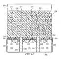
- FIGS. 1 through 4show cross-sectional views of a prior art method of fabricating a 3D-IC
- FIGS. 5 through 11show cross-sectional views of a method of manufacturing a 3D-IC in accordance with a preferred embodiment of the present invention, wherein deep vias for vertical connection of the 3D-IC are formed within a top portion of a workpiece early in the manufacturing process, before the BEOL, and wherein two ICs are vertically coupled together face-to-face;
- FIGS. 12 through 14show cross-sectional views of a method of manufacturing a 3D-IC in accordance with another preferred embodiment of the present invention, wherein two ICs are vertically coupled together back-to-face;
- FIGS. 15 through 20show cross-sectional views of a method of manufacturing a 3D-IC in accordance with yet another embodiment of the present invention, wherein deep vias are formed before active areas are formed within the workpiece, simultaneously with the formation of trenches for other features of the IC;
- FIG. 21shows an embodiment of the present invention, wherein a passivating capping layer is formed over the conductive material of the deep vias formed within the top portion of the workpiece, and wherein voids may form in the deep via trenches.
- FIGS. 1 through 4show cross-sectional views of a prior art method of fabricating a 3D-IC at various stages of manufacturing.
- integrated circuit 102 acomprises a workpiece 101 a .
- Active areas 108 aare formed within and over the workpiece 101 a , as shown.
- the active areas 108 amay include transistors, as shown, or the active areas 108 a may comprise other devices or circuit components.
- the workpiece 101 a and the active areas 108 aare labeled 106 a to indicate the portion of the integrated circuit 102 a that is processed in a front end of line (FEOL) manufacturing process, e.g., before any metallization layers are deposited.
- FEOLfront end of line
- An interconnect regioncomprising conductive lines 110 a and conductive vias 111 a formed in an insulating material 112 a is formed over the workpiece and the active areas 108 a .
- the interconnect regionmay comprise one or more conductive layers within an insulating material layer, and may comprise a multi-layer interconnect region formed by subtractive etch processes or damascene processes, for example.
- the interconnect regionis labeled 104 a to indicate the portion of the integrated circuit 102 a that is processed in the back end of line (BEOL), e.g., after the first metallization layer is deposited.
- BEOLback end of line
- Integrated circuit 102 bmay comprise similar components and elements as integrated circuit 102 a , as indicated by similar element numbers with a “b” suffix. Integrated circuit 102 b may comprise a similar circuit or a different type of circuit as the circuit formed on integrated circuit 102 a , for example.
- One prior art method of forming a 3D-IC 100is to invert one integrated circuit 102 a and bond the top surface of integrated circuit 102 a to the top surface of integrated circuit 102 b , as shown in FIG. 2 .
- This type of vertical connection of two integrated circuits 102 a and 102 bis often referred to as “face-to-face” bonding.
- Integrated circuit 102 amay comprise an entire wafer or a single die
- integrated circuit 102 btypically comprises an entire wafer, for example, although alternatively, both the integrated circuit 102 a and integrated circuit 102 b may comprise single die.
- the integrated circuits 102 a and 102 bare bonded at a bond region 114 , as shown, using an adhesive (e.g., comprising bond region 114 ), such as benzocyclobutene (BCB) or a polyimide, as examples.
- an adhesivee.g., comprising bond region 114
- the integrated circuits 102 a and 102 bmay also be bonded using oxide bonds (e.g., by bonding together the insulating materials 112 a and 112 b ) or metal bonds (e.g., by bonding together some of conductive lines 110 a and 110 b ), not shown.
- the top surfacee.g., the workpiece 101 a of the top integrated circuit 102 a
- the workpiece 101 ais ground, etched, and/or polished using a thinning process 116 , reducing the thickness of the workpiece 101 a .
- deep vias 118are formed in the top integrated circuit 102 a , as shown in FIG.
- the deep vias 118extend through the entire thickness of the top integrated circuit 102 a and through the bond region 114 , and in some designs, extend partially through the bottom integrated circuit 102 b , as shown.
- the deep vias 118provide electrical connection between regions 117 a in the top integrated circuit 102 a and regions 119 b in the bottom integrated circuit 102 b , as shown.
- a hard mask(not shown) is typically deposited over the thinned workpiece 101 a , and a layer of photoresist is deposited over the hard mask and patterned with the desired pattern for the deep vias 118 .
- the layer of photoresistis then used as a mask to pattern the hard mask.
- the hard maskis then used to pattern the various material layers 101 a , 108 a , 112 a , 111 a , and 110 a of the top integrated circuit 102 a , the bond region 114 , and material layers (e.g., insulating material 112 b ) of the bottom integrated circuit 102 b , forming trenches for the deep vias.
- An insulating lineris formed within the trenches (not shown in FIG. 4 ).
- the insulating lineris opened at the bottom of the trenches by directionally etching the liner, leaving the insulating liner on the sidewalls of the trenches.
- a conductive materialis then deposited over the 3D-IC 100 to fill the deep vias 118 , as shown in FIG. 4 .
- a problem with the prior art method of forming the deep vias 118 shownis that there are several material layers 101 a , 108 a , 112 a , 111 a , 110 a , 114 , and 112 b that must be etched, causing the etch process to be lengthy, time-consuming, and costly.
- the etch processis also difficult to control. Because many different types of materials must be etched, the etch chemistries may need to be changed several times, e.g., about 10 to 15 or more times, because different etch chemistries are required to etch different material types.
- the insulating liner on the sidewalls of the trenches for the deep vias 118cannot be formed using a high temperature thermal nitridation process or by thermal oxidation, because the interconnect regions of the two ICs 102 a and 102 b include metals (e.g., conductive lines 110 a , 110 b , and vias 111 a and 11 l b ); thus, the temperature that the 3D-IC 100 may be exposed to is limited to about 400 degrees C. or less.
- a thermal nitridation process to form a layer of Si x N y or a thermal oxidation process to form a liner of SiO 2may require temperatures of about 700 degrees C. or more, for example.
- PVDphysical vapor deposition
- PE CVDPlasma Enhanced Chemical Vapor Deposition
- deep viasare required to be made in the workpiece 101 a of the top IC 102 a , to make electrical contact to the active areas 108 a or to the conductive lines 110 a and vias 111 a . While fewer material layers must be etched in this case to form the deep vias, high temperature processes may still not be used to form the insulating liner of the deep vias because of the presence of the metallization layers of the interconnect regions of the two ICs 102 a and 102 b , as described above.
- Another method used to vertically integrate integrated circuits 102 a and 102 bis to bond two ICs 102 a and 102 b “front-to-back,” e.g., wherein a bottom surface of one IC 102 a is bonded to a top surface of another IC 102 b (not shown in the drawings).
- the integrated circuite.g., such as IC 102 a in FIG. 1
- the carrier wafernot shown
- the bottom surface of the thinned integrated circuit 102 ais attached to the top surface of the other integrated circuit 102 b .
- this methodalso requires etching many different material layers to form the deep vias for making electrical connection between the vertically stacked ICs, and forming the insulating liner within the trenches is limited to low temperature deposition methods.
- an additional signal distribution layermay be needed to make the required electrical connections, not shown in the drawings.
- the signal distribution layercomprises an additional interconnect layer that is used to make the vertical connections between the two ICs.
- Embodiments of the present inventionprovide technical advantages by forming deep vias for providing electrical connection for vertically stacked integrated circuits early in the manufacturing process, before the integrated circuits are vertically attached to other integrated circuits.
- fewer material layersare required to be etched during the formation of the deep vias, which provides several advantages, to be described further herein.
- the deep viasare formed before any metals are deposited (e.g., before the BEOL), so that high temperature processes may be used to form an insulating liner on sidewalls of the trenches of the deep vias.
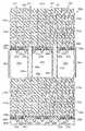
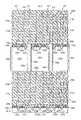
- FIGS. 5 through 11show cross-sectional views of a method of manufacturing a 3D-IC in accordance with a preferred embodiment of the present invention.
- the workpiece 201may include a semiconductor substrate comprising silicon or other semiconductor materials covered by an insulating layer, for example.
- the workpiece 201may also include other active components or circuits, not shown.
- the workpiece 201may comprise silicon oxide over single-crystal silicon, for example.
- the workpiece 201may include other conductive layers or other semiconductor elements, e.g., transistors, diodes, etc. Compound semiconductors, GaAs, InP, Si/Ge, or SiC, as examples, may be used in place of silicon.
- the workpiece 201may comprise a silicon-on-insulator (SOI) substrate, for example.
- SOIsilicon-on-insulator
- the workpiece 201may comprise a thickness of about 600 ⁇ m, yet only the upper 25 ⁇ m is shown in the drawings, for example.
- Active areas 222 / 224are formed proximate the top surface of the workpiece 201 , as shown.
- transistors 224may be formed proximate the workpiece 201 top surface, e.g., by implanting dopant regions within the top surface of the workpiece 201 , and forming gate dielectrics, gates, and sidewall spacers over the doped regions.
- the transistors 224may be separated by isolation regions 222 formed in the top surface of the workpiece 201 between adjacent transistors 224 , also shown.
- the isolation regions 222may comprise a depth within the top surface of the workpiece 201 of about 2,000 Angstroms or less, for example, although alternatively, the isolation regions 222 may comprise a depth of greater than 2,000 Angstroms.
- the transistors 224may comprise p channel field effect transistors (PFETs) and n channel field effect transistors (NFETs) arranged in complementary configurations, e.g., to form complementary metal oxide semiconductor (CMOS) devices, for example.
- the transistors 224may also comprise bipolar transistors or other thin film transistors, or combinations thereof with CMOS devices, as examples.
- An insulating material 226comprising silicon dioxide or other dielectric material may be deposited over the active areas 222 / 224 , as shown.
- the active areas 222 / 224are preferably formed using FEOL processes (e.g., region 206 is formed in a FEOL), for example.
- the active areas 222 / 224may comprise transistors, as shown, and alternatively may comprise memory devices, switches, diodes, capacitors, logic circuits, other electronic components, or combinations thereof with transistors (not shown), formed within and above the workpiece 201 , as examples.
- a hard mask 236is deposited over the active areas 222 / 224 and insulating material 226 , as shown in FIG. 6 .
- the hard mask 236preferably comprises a first layer 230 that may function as an etch stop layer, comprised of a nitride material such as silicon nitride, silicon carbon, or other insulating material different than the second layer 232 material, for example.
- the hard mask 236preferably also includes a second layer 232 disposed over the first layer 230 , as shown.
- the second layer 232may comprise an oxide, a doped oxide, or other masking materials such as boron-doped silicon glass (BSG), as examples.
- BSGboron-doped silicon glass
- the hard mask 236may comprise a thickness of about 1 ⁇ m, although alternatively, the hard mask 236 may comprise other dimensions.
- the hard mask 236may alternatively comprise a single type of material, a single layer, or three or more material layers, as examples.
- a layer of photoresist 234is deposited over the hard mask 236 .
- the layer of photoresist 234is patterned using lithography (e.g., by exposing portions the layer of photoresist 234 using a lithography mask, and developing the layer of photoresist 234 ) with the desired shape of the deep vias, as shown in FIG. 6 .
- the pattern for the deep viaspreferably comprises a width of about 0.5 to 3.0 ⁇ m, and more preferably comprises a width of about 1.0 ⁇ m in this embodiment, as examples, although alternatively, the width of the deep vias may comprise other dimensions.
- the layer of photoresist 234is then used to pattern the hard mask 236 .
- the layer of photoresist 234is used as a mask while exposed portions of the hard mask 236 are removed, as shown in FIG. 7 .
- the layer of photoresist 234may be left remaining over the hard mask 236 after the hard mask 236 is patterned, or the layer of photoresist 234 may be partially or completely consumed during the patterning of the hard mask 236 .
- the hard mask 236 and optionally also the photoresist 234is then used as a mask to pattern trenches for deep vias in the insulating layer 226 , active areas 222 / 224 , and in a top portion 220 of the workpiece 201 , as shown in FIG. 7 .
- the etch process 238 to form the deep viaspreferably comprises a dry etch process, although other etching methods may also be used.
- the trenches for the deep viaspreferably comprise a depth d 1 of about 5 to 25 ⁇ m, and more preferably comprise a depth d 1 of about 20 ⁇ m, below the active areas 222 / 224 of the workpiece 201 , as shown. Alternatively, depth d 1 of the trenches for the deep vias may comprise other dimensions.
- the width d 2 of the trenches for the deep viaspreferably comprises substantially the same width as the pattern of the layer of photoresist, as shown.
- a portion of the hard mask 236may be consumed during the etch process used to form the trenches for the deep vias, e.g., the thickness of the second layer 232 of the hard mask 236 may be reduced after the etch process 238 .
- At least a portion of the hard mask 236may be removed.
- the second layer 232 of the hard mask 236may be removed, e.g., using a dry or wet etch process, or a chemical-mechanical polish (CMP) process adapted to stop on the first layer 230 that functions as an etch stop layer for the removal of the second layer 232 , as examples.
- the first layer 230may be left remaining in the structure, or alternatively, the first layer 230 may also be removed.
- a liner 240is formed within the trenches for the deep vias, and the trenches for the deep vias are filled with a conductive material 242 , as shown in FIG. 8 .
- the liner 240is formed on the sidewalls and bottom surface of the trenches for the deep vias, as shown in FIG. 8 .
- the liner 240preferably is formed by a thermal process, e.g., by thermal nitridation or thermal oxidation at temperatures greater than about 400 degrees C., and in some embodiments, the liner 240 is formed at temperatures greater than about 700 degrees.
- the liner 240may be formed by oxidation, nitridation, deposition, or combinations thereof, for example.
- the liner 240preferably comprises an insulating material disposed on the sidewalls and bottom surface of the trenches.
- the liner 240may also optionally include one or more barrier layers, a seed layer, or both, formed over the insulating material, for example.
- the liner 240may comprise a thickness of about 500 Angstroms or less, for example.
- the liner 240may comprise SiO 2 , Si x N y , SiON, other nitride materials, Ta, TaN, TiN, Cu, Ru, combinations thereof, or multiple layers thereof, as examples, although other materials may also be used.
- a relatively high temperaturee.g., greater than about 400 degrees C.
- an insulating portion of the liner 240is formed at a temperature of about 700 degrees C. or greater, in accordance with an embodiment of the present invention.
- the formation of the novel deep viasis not restricted to temperature limits for BEOL processes, advantageously.
- the liner 240may be left remaining on the bottom surface of the trenches, e.g., the insulating portion of the liner 240 is not required to be removed from the bottom surface of the trenches for the deep vias.
- the liner 240preferably comprises a material suitable to provide a barrier for diffusion of the copper into adjacent material such as the workpiece 201 and the active areas 222 / 224 , for example.
- the liner 240preferably comprises a diffusion barrier layer of Ta, TaN, or both, e.g., a bilayer of Ta/TaN.
- the liner 240may include a seed layer comprising Cu or Ru, for example, for the formation of the copper conductive material 242 , if a plating process is used to fill the trenches, for example.
- the liner 240may comprise a thin layer of SiO 2 , Si x N y , or other insulating material formed within the trenches before the seed layer and/or diffusion barrier layer is formed, for example.
- the conductive material 242 and liner 240may be formed by: first; forming the liner 240 over the top surface of the first layer 230 of the hard mask and over the sidewalls and bottom surface of the trenches, using chemical vapor deposition (CVD), physical vapor deposition (PVD), atomic layer deposition (ALD), or other deposition techniques, and second; depositing or plating the conductive material 242 over the liner 240 , filling the trenches and covering the liner 240 on the top surface of the first layer 230 (or insulating material 226 if the first layer 230 of the hard mask 236 has been removed).
- CVDchemical vapor deposition
- PVDphysical vapor deposition
- ALDatomic layer deposition
- the conductive material 242may comprise Cu, W, Ru, TiN, combinations thereof, other metals, combinations of two or more metals, or a semiconductive material such as silicon, doped silicon, or polysilicon, as examples.
- a CMP processmay then be used to remove excess conductive material 242 and the liner 240 from over the top surface of the first layer 230 of the hard mask 236 , leaving the structure shown in FIG. 8 .
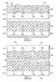
- a BEOL processis then used to form an interconnect region 210 / 211 / 212 over the workpiece 201 , e.g., over the first layer 230 of the hard mask, if left remaining in the structure, as shown in FIG. 9 , or over the insulating material 226 , if the first layer 230 has been removed.
- the BEOL processmay comprise forming a plurality of insulating material layers 212 and forming alternating layers of vias 211 and conductive lines 210 in the insulating material layers 212 , e.g., using subtractive etch processes and/or damascene etch processes.
- the insulating material layers 212may include etch stop layers, SiO 2 layers, other insulating materials, and/or low dielectric constant (k) materials, e.g., having a dielectric constant of less than about 3.9, for example.
- the conductive lines 210 and vias 211may comprise Cu, W, other metals, or combinations thereof, as examples.
- the interconnect region 210 / 211 / 212preferably comprises at least one layer of conductive lines 210 disposed within an insulating material layer 212 , although in other embodiments, the interconnect region 210 / 211 / 212 preferably comprises a plurality of conductive line 210 layers and via 211 layers disposed within a plurality of insulating material layers 212 , as shown in FIG. 9 .
- the BEOL processeffectively begins with the filling of the deep via trenches, in this embodiment, because a first metal layer is deposited with the filling of the deep via trenches.
- FEOL processesinclude high temperature processes such as anneal processes that cannot be performed after some metals are deposited, for example.
- the maximum temperature of a BEOL processmay be about 400 degrees C., whereas temperatures may reach about 1,050 degrees C. in some FEOL processes, for example.
- a novel IC 250is formed having deep vias 240 / 242 formed in a top portion 220 of the workpiece 201 , as shown in FIG. 9 , in accordance with embodiments of the present invention.
- the deep vias 240 / 242have been formed before the IC 250 is vertically integrated to another workpiece or IC 250 .
- the deep vias 240 / 242are formed in the workpiece 201 after the formation of the active areas 222 / 224 in this embodiment.
- the IC 250may be vertically attached face-to-face (top surface to top surface) to another IC, as shown in FIGS. 10 and 11 , or back-to-face, (bottom surface to top surface) to another IC, as shown in FIGS. 12 through 14 , as will next be described.
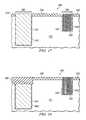
- FIGS. 10 and 11Face-to-face vertical attachment of the novel IC 250 to another IC in accordance with an embodiment of the present invention is illustrated in FIGS. 10 and 11 .
- a first integrated circuit 250 ais attached to a second integrated circuit 250 b by bonding the top surface of the first interconnect region 210 a / 211 a / 212 a to the top surface of the second interconnection region 210 b / 21 l b / 212 b , e.g., at 252 , as shown in FIG. 10 .
- the bonding of the first interconnect region 210 a / 211 a / 212 a to the second interconnection region 210 b / 21 l b / 212 bpreferably comprises a metal-to-metal bond that provides electrical connection between portions of the first interconnect region 210 a / 211 a / 212 a to the second interconnection region 210 b / 21 l b / 212 b .
- the metal-to-metal bondsmay be formed by activating the surfaces of the conductive lines 210 a and 210 b , positioning the ICs 250 a and 250 b so that some of the conductive lines 210 a and 210 b align, and applying temperature and/or pressure to the ICs 250 a and 250 b to bond the conductive lines 210 a and 210 b together, for example.
- the mating surfacese.g., the surfaces of the conductive lines 210 a and 210 b , and also the insulating materials 212 a and 212 b
- the mating surfacesare preferably extremely clean, smooth, (e.g., preferably having a surface roughness of less than about 10 ⁇ root mean square (RMS)) and globally coplanar.
- RMSroot mean square
- an adhesiveis not used for the face-to-face bonding, so that electrical connection of the conductive lines 210 a and 210 b of the first interconnect region 210 a / 211 a / 212 a and the second interconnection region 210 b / 21 l b / 212 b , respectively, is achieved.
- the workpiece of the top IC 250 ais thinned using a thinning process 254 , as shown in FIG. 11 , removing a portion of the workpiece 201 a , e.g., the lower portion (which appears as an “upper” portion in FIG. 10 because the workpiece 201 a has been inverted) of the workpiece 201 a .
- the thinning process 254may comprise an etch process, a grinding process, a CMP process, a polishing process, or combinations thereof, as examples.
- the upper portion 220 a of the workpieceis left remaining, with the ends of the deep vias 242 a / 240 a left exposed.
- the remaining thickness of the upper portion 220 a of the workpiece 201may comprise about 25 ⁇ m or less, for example.
- the deep vias 240 a / 242 aprovide electrical connection through the workpiece 201 a to the active areas 222 a / 224 a.
- At least the insulating portion of the liner 240is removed from the ends of the deep vias 240 a / 242 a during the thinning process 254 so that the exposed ends of the deep vias 240 a / 242 a are conductive and may be connected to other circuitry, e.g., to an external connection of the 3D-IC 260 (not shown), or vertically to another IC 250 , for example (also not shown).
- Bond pads(not shown) may be formed over the ends of the deep vias 240 a / 242 a , and a passivation layer (not shown) may be deposited between the bond pads.
- the bond padsmay be positioned adjacent the ends of the deep vias 240 a / 242 a , providing an electrical connection.
- the workpiece 201 b of the bottom IC 250 bmay be thinned by attaching the top of the 3D-IC to a carrier wafer or workpiece and thinning the workpiece 201 b , wherein after the thinning process, the bottom workpiece 201 b comprises a thickness of about 300 ⁇ m, for example.
- the 3D-IC 260may be placed in a package or circuit board, e.g., by attaching the bottom surface of the workpiece 201 b to the package or circuit board. Wires may then be bonded to the bond pads, and the other end of the wires may be attached to pins of the package or other ICs attached to the circuit board.
- the lower workpiece 201 bmay be grounded or coupled to a return voltage, for example.
- the deep vias 240 a / 242 aprovide electrical connection to the conductive portion 224 a of the active areas 222 a / 224 a of the top IC 250 a through the workpiece 201 a .
- the deep vias 240 a / 242 aalso provide electrical connection to the conductive portion 224 b of the active areas 222 b / 224 b of the bottom IC 250 b , e.g., through the conductive lines and vias 210 a , 211 a , 210 b , and 21 l b.
- a 3D-IC 260is formed, wherein two ICs 250 a and 250 b are bonded together at their interconnect regions 210 a / 211 a / 212 a and 210 b / 211 b / 212 b , and wherein at least one of the ICs 250 a comprise deep vias 240 a / 242 a formed in the workpiece 201 a to provide electrical connection to the active areas 222 a / 224 a .
- the lower IC 250 bdoes not include a novel deep via described herein; however, similar element numbers are used in the lower IC 250 b as in the upper IC 250 a .
- both ICs 250 a and 250 bmay have deep vias 240 a / 242 a formed therein (not shown in IC 250 b ).
- the lower IC 250 bwould include deep vias (not shown), and before or after the workpiece 201 a is thinned for IC 250 a , the workpiece 201 b of the lower IC 250 b is thinned by attaching a carrier wafer (see carrier wafer 262 shown in FIG. 12 ) to the workpiece 201 a of IC 250 a , and then thinning the workpiece 201 b to expose the ends of the deep vias, as described with reference to FIG. 11 , using a thinning process 254 .
- a carrier wafersee carrier wafer 262 shown in FIG. 12
- FIGS. 12 through 14Back-to-face vertical attachment of the novel IC 250 to another IC in accordance with an embodiment of the present invention is illustrated in FIGS. 12 through 14 .
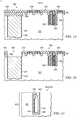
- an integrated circuit 250is attached to a carrier wafer 262 at the top surface of the interconnect region 210 / 211 / 212 , as shown in FIG. 12 .
- the carrier wafer 262may comprise a semiconductor wafer or workpiece blank that is used to support the IC 250 and provide handling capability during the thinning of the workpiece 201 , for example.
- the workpiece 201is thinned using a thinning process 264 , as shown in FIG.
- the thickness of the workpiece 201 after the thinning processpreferably comprises about 20 ⁇ m or less, for example.
- the thinning processes 254 and 264 described hereinmay include an end point detection means, e.g., so that the process may be stopped when the deep via 240 / 242 material is reached, or stopped after a predetermined time after the deep vias 240 / 242 material is reached.
- the thinning processes 254 and 264may comprise a timed thinning process, for example.
- the insulating portion of the deep vias 240 / 242e.g., at least a portion of the liner 240 is preferably removed during the thinning process 264 .
- the thinned surface 266 a of the workpiece 201 a of the integrated circuit 250 ais then vertically coupled, e.g., attached or bonded to another integrated circuit 250 b .
- the lower IC 250 bdoes not include a novel deep via described herein; however, similar element numbers are used in the lower IC 250 b as in the upper IC 250 a .
- both ICs 250 a and 250 bmay have deep vias 240 a / 242 a formed therein (not shown in IC 250 b ), as described with reference to FIG. 11 .
- the deep vias 240 a / 242 apreferably make electrical connection to a portion of the interconnect region 210 b / 211 b / 212 b , e.g., to a top portion of conductive lines 210 b , as shown.
- the conductive lines 210 bmay be bonded to the exposed ends of the deep vias 240 a / 242 a by metal-to-metal bonds, for example.
- a 3D-IC 270is formed wherein the deep vias 240 a / 242 a provide vertical electrical connection between conductive portions 224 a of the active areas 222 a / 224 a and conductive portions 224 b of the active areas 222 b / 224 b of the two ICs 250 a and 250 b , respectively, e.g., through conductive lines 210 b and vias 211 b .
- electrical connectionmay be made to the interconnect region 210 a / 211 a / 212 a of the upper IC 250 a by external circuitry or bond pads or vertically by another IC (not shown).
- the conductive lines 210 amay be coupled to bond pads of the device, for example, not shown.
- the workpiece 201 bmay be thinned and mounted to a package or circuit board, and the carrier wafer 262 (shown in FIG. 13 ) is removed.
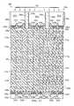
- FIGS. 15 through 20show cross-sectional views of a method of manufacturing a 3D-IC in accordance with yet another embodiment of the present invention, wherein the novel deep vias described herein are formed even earlier in the manufacturing process of the IC 380 .
- the deep via trenchesare formed simultaneously with the formation of other trenches of the semiconductor device in the FEOL, before the formation of transistors and other active areas.
- deep trenchesmay be formed during the FEOL. Deep trenches may be used to form capacitors in memory arrays and other structures, as examples. Deep trenches may also be used to form isolation structures, for example. These deep trenches may have a depth of about 10 nm or less within a top surface of a workpiece, for example, and may comprise a minimum feature size or larger.
- a workpiece 301is provided.
- a hard mask 336is formed over the workpiece 301 .
- the hard mask 336may include a first layer 330 and a second layer 332 , and alternatively may comprise a single layer or two or more layers.
- the hard mask 336is patterned with a pattern 382 for deep vias and also a pattern 384 for trenches of other structures of the integrated circuit 380 , as shown.
- the trenches of the pattern 382 for the deep viaspreferably comprise a width d 3 that is greater than the width d 4 of the trenches of pattern 384 , as shown.
- the width d 3 of the deep via trenchesmay comprise about 5 to 25 ⁇ m or less
- the width d 4 of the trenches of the pattern 384may comprise a minimum feature size of the integrated circuit 380 , e.g., about 400 nm or less, e.g., 70 to 90 nm or less.
- the etch process 338is used to form trenches in the workpiece 301 , as shown in FIG. 16 .
- the etch process 338preferably comprises a reactive ion etch (RIE), although other etch processes may also be used.
- RIEreactive ion etch
- the etch processpreferably comprises an etch process wherein wide patterns will etch faster than narrower patterns, for example, in accordance with a preferred embodiment of the present invention. If the etch process 338 comprises a RIE process, for example, RIE lag results in the formation of shallower trenches having a depth d 6 being formed in the narrow patterns and deeper trenches having a depth d 5 within the workpiece 301 , as shown.
- the depth d 6preferably comprises about 10 ⁇ m or less, and may comprise about 4 to 8 ⁇ m, for example.
- the depth d 5preferably comprises about 20 ⁇ m, or about 5 to 25 ⁇ m, for example.
- the trench depths d 5 and d 6may comprise other dimensions.
- the trenches of patterns 382 and 384may then be filled with a liner 340 and a conductive material 342 , as shown in FIG. 17 .
- the liner 340may comprise SiO 2 and the conductive material 342 preferably comprises polysilicon or other semiconductive materials, in a preferred embodiment.
- the pattern 384comprises a pattern for a plurality of capacitors, then preferably the conductive material 342 comprises polysilicon.
- the material 342 used to fill the wider deep via shown on the left side of FIG. 17may comprise polysilicon, a metal, or both, for example.
- the wider deep viamay be filled in partially or completely with the material 342 that the shallower trenches on the right side of the figure is filled with, for example.
- the wider deep viamay also be temporarily filled with the shallower via material, e.g., the material 342 within the wider deep via may comprise a sacrificial plug material that is later removed and replaced with a lower resistivity material, such as a metal.
- the deep via on the left side of the figuremay be protected during transistor processing, e.g., during the lithography process, etch, fill, and planarization processing steps, as shown in FIG. 18 .
- a top portion of the deep via trenchmay be masked with an insulating material 386 such as SiO 2 or SiN, or other materials, which may be removed later and filled with a conductive material, such as a metal, in a BEOL process.
- the insulating material 386may be left remaining over the deep via while active areas (e.g., transistors) are formed in a FEOL process (e.g., the processing of material layers 390 ).
- the insulating material 330may be opened up over the deep via, as shown in FIG. 19 and the top portion 388 of the deep via, shown in FIG. 20 , may then be filled with a conductive material, e.g., as part of a BEOL process, for example (not shown).
- the top portion of the deep via trenchmay be filled with a metal during a BEOL process to form the first layer of the interconnect region (e.g., such as region 210 a / 211 a / 212 a shown in FIG. 9 .
- the deep via trenches on the left sidemay be filled with a different material than the shallower trenches on the right side of the drawing, not shown in the drawings.
- the deep via trenchese.g., pattern 382 in FIG. 17
- the shallower trenchesmay be filled with highly doped polysilicon.
- One side of the workpiece 301may be covered with a mask while the other side is filled and/or implanted with dopants, for example, so that the conductive material 342 is different in the deep vias and the shallower trenches.
- the pattern 384comprises isolation trenches
- the shallower trenchesmay be filled with an insulating material, for example, wherein the deep via trenches of pattern 382 are filled with a conductive material.
- interconnect regionsare formed (not shown in FIGS. 15 through 20 ), as described with reference to FIGS. 5 through 14 .
- Two or more ICs 380are bonded together and vertically integrated using the novel deep vias 340 / 342 described herein.
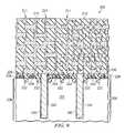
- the fill process used to form the conductive material 442may result in the formation of a non-conformal fill and/or a non-bottom-up fill, which may lead to the formation of voids 494 within the trenches for the deep vias.
- voids 494may lead to the formation of voids 494 within the trenches for the deep vias.
- Like numeralsare used for the elements in FIG. 21 as were used to describe the previous figures, and again, to avoid repetition, each reference number shown in FIG. 21 is not described again in detail herein.
- the filling of the conductive material 442 in the trenchesmay tend to pinch off the conductive material 442 at the top of the trenches before the trenches are completely filled, for example.
- a capping layer 492comprising an insulator is formed over the conductive material 442 , as shown in FIG. 21 .
- the thickness of the conductive material 442 and the capping layer 492may depend on the width of the trenches, for example.
- the conductive material 442may comprise a thickness of greater than about 500 nm to several ⁇ m, for example.
- the capping layer 492preferably comprises an insulating material, such as SiC, SiCN, or SiN, as examples, although other passivating materials may also be used.
- the capping layer 492preferably comprises a thickness of about 30 nm or greater, and more preferably comprises a thickness of about 100 nm or greater, for example.
- the capping layer 492passivates the conductive material 442 .
- the capping layer 492may be deposited using a spin-on process to completely fill the area within the trenches for the deep vias above the conductive material 442 , in one embodiment. However, other deposition processes may be used that are conformal and may result in the pinching off of the capping layer 492 at the top of the trenches, as shown in FIG. 21 , forming a void 494 within the capping layer 492 . Excess portions of the capping layer and the conductive material 442 are then removed using a CMP process, etch process, or combinations thereof, leaving the structure shown in FIG. 21 .
- the voids 494 that may optionally be formed within the capped conductive material 442do not present a problem and may be left remaining in the structure if properly processed (for example, if the conductive material 442 is covered with the capping layer 492 ), because the conductive material 442 still provides a path for electrical conduction from one end of each deep via 440 / 442 to the other end, for example.
- a capping layer 492 or a capping layer 492 with voids 494 formed thereinmay be formed in the trenches for the deep vias 240 / 242 and 340 / 342 in the embodiments of the present invention shown in FIGS. 5 through 14 , and also in the embodiments of the present invention shown in FIGS. 15 through 20 , for example.
- Advantages of embodiments of the inventioninclude providing novel integrated circuit structures and methods of fabrication thereof, wherein deep vias 240 / 242 , 340 / 342 , and 440 / 442 for vertical connection to other ICs are formed before two ICs are vertically coupled together. Fewer material layers are required to be etched, because the deep vias 240 / 242 , 340 / 342 , and 440 / 442 are formed earlier in the manufacturing process of the integrated circuit, which results in an improved process window.
- endpoint detectionmay be used to determine when the end of the deep via 240 / 242 , 340 / 342 , and 440 / 442 is reached and thus exposed.
- Signal routingis made more flexible by the use of embodiments of the present invention, and less interconnect “real estate” is used on an integrated circuit.
- the deep vias 240 / 242 , 340 / 342 , and 440 / 442are formed early in the manufacturing process, e.g., before the BEOL, it is not necessary to reserve space in the BEOL circuitry, e.g., in the interconnect region, for the placement of the deep vias 240 / 242 , 340 / 342 , and 440 / 442 .
- spacemust be reserved for the deep vias within the interconnect region pattern, because some metals such as Cu cannot be etched, for example.
- the deep via regionscannot be used for interconnect, and dummy patterns cannot be used in the reserved deep via regions, which are often used in the fabrication process to reduce dishing during CMP processes, which can occur when damascene processes are used to form conductive lines.
- a higher interconnect integration densitymay be achieved, and dummy patterns may be formed (e.g., in the material layers for conductive lines 210 a and 210 b and vias 211 a and 211 b within the insulating material layers 212 a and 212 b ) that improve the CMP process and avoid dishing of the conductive features 210 a , 210 b , 211 a , and 211 b.
- the novel deep vias 240 / 242 , 340 / 342 , and 440 / 442 formed early in the manufacturing process at the single die level or at the wafer levelallow the use of an insulating liner 240 , 340 , and 440 for the deep vias 240 / 242 , 340 / 342 , and 440 / 442 that may be formed using a high temperature thermal process, e.g., at temperatures of about 400 degrees or greater, and more preferably at temperatures of about 700 degrees or more, in some embodiments, resulting in the formation of liners 240 , 340 , and 440 having improved insulating properties and improved step coverage, for example.
- the interface characteristics of the liners 240 , 340 , and 440may comprise a high quality comparable to the interface characteristics of gate oxides of transistors, for example.
- the workpiece 201 , 301 , and 401may be thinned to a thickness of less than about 100 ⁇ m, decreasing the vertical size of the 3D-IC.
- the workpiece 201 , 301 , and 401may be thinned to a thickness of greater than or equal to 100 ⁇ m, which may be an advantage in some applications.
- a dedicated interconnect layer for routing connections between two vertically stacked ICsis not required by embodiments of the present invention. Rather, the deep vias 240 / 242 , 340 / 342 , and 440 / 442 provide the vertical interconnection for the 3D-ICs 260 and 270 .
Landscapes
- Engineering & Computer Science (AREA)
- Microelectronics & Electronic Packaging (AREA)
- Power Engineering (AREA)
- Computer Hardware Design (AREA)
- Physics & Mathematics (AREA)
- Condensed Matter Physics & Semiconductors (AREA)
- General Physics & Mathematics (AREA)
- Manufacturing & Machinery (AREA)
- Internal Circuitry In Semiconductor Integrated Circuit Devices (AREA)
Abstract
Description
- The present invention relates generally to the fabrication of semiconductor devices, and more particularly to the fabrication of vertically stacked integrated circuits.
- Semiconductor devices are used in a variety of electronic applications, such as computers, cellular phones, personal computing devices, and many other applications. Home, industrial, and automotive devices that in the past comprised only mechanical components now have electronic parts that require semiconductor devices, for example.
- Semiconductor devices are manufactured by depositing many different types of material layers over a semiconductor workpiece or wafer, and patterning the various material layers using lithography. The material layers typically comprise thin films of conductive, semiconductive, and insulating materials that are patterned and etched to form integrated circuits (ICs). There may be a plurality of transistors, memory devices, switches, conductive lines, diodes, capacitors, logic circuits, and other electronic components formed on a single die or chip, for example.
- After an integrated circuit is manufactured, individual die are singulated from the wafer, and typically, the die is packaged. For many years, the most common way of packaging a die was horizontal placement within individual plastic or ceramic packages. Alternatively, several die may be packaged horizontally in a single package, forming a multi-chip module. Electrical connections are made to terminals or bond pads of the die, e.g., using very small strands of wire, which is routed to pins of the package.
- A demand for smaller ICs with higher performance has led to the development of system-on-a-chip devices, where portions of the chip are dedicated to memory and other portions are dedicated to logic or other types of circuitry. However, it can be difficult to manufacture an IC with multiple types of circuitry, due to integration problems of the different circuit fabrication technologies.
- One trend in the semiconductor industry is the movement towards three dimensional integrated circuits (3D-ICs), for example, where two or more chips or wafers are stacked and vertically integrated. Parts of a circuit are fabricated on different wafers, and the wafers or die are bonded together with a glue layer such as copper or a polymer based adhesive. Different types of circuits, e.g., memory and logic, as examples, may be manufactured separately and then vertically attached, which may be less expensive and easier to manufacture than combining the two circuit technologies on a single wafer as in system-on-a-chip devices. 3D-ICs are predicted to be used in the future for low power, high speed applications, because the paths of conduction may be shortened by the vertical electrical connections between the circuits, resulting in low power consumption and increased speed.
- However, 3D-ICs introduce some design and fabrication challenges. For example, the etch processes required to produce the vertical connections between vertically stacked ICs may be difficult, due to the many different types of material layers and the thickness of the material layers that must be etched.
- Thus, improved methods of fabricating 3D-ICs and structures thereof are needed in the art.
- These and other problems are generally solved or circumvented, and technical advantages are generally achieved, by preferred embodiments of the present invention, which provide novel methods of connecting two or more ICs together to form 3D-ICs and structures thereof.
- In accordance with a preferred embodiment of the present invention, a method of fabricating a semiconductor device includes fabricating a first integrated circuit, fabricating a second integrated circuit, and vertically coupling the second integrated circuit to the first integrated circuit. Fabricating the first integrated circuit includes providing a first workpiece, forming at least one first active area within the first workpiece, and forming at least one deep via within the first workpiece, wherein the at least one deep via provides vertical electrical connection for the first integrated circuit.
- The foregoing has outlined rather broadly the features and technical advantages of embodiments of the present invention in order that the detailed description of the invention that follows may be better understood. Additional features and advantages of embodiments of the invention will be described hereinafter, which form the subject of the claims of the invention. It should be appreciated by those skilled in the art that the conception and specific embodiments disclosed may be readily utilized as a basis for modifying or designing other structures or processes for carrying out the same purposes of the present invention. It should also be realized by those skilled in the art that such equivalent constructions do not depart from the spirit and scope of the invention as set forth in the appended claims.
- For a more complete understanding of the present invention, and the advantages thereof, reference is now made to the following descriptions taken in conjunction with the accompanying drawings, in which:
FIGS. 1 through 4 show cross-sectional views of a prior art method of fabricating a 3D-IC;FIGS. 5 through 11 show cross-sectional views of a method of manufacturing a 3D-IC in accordance with a preferred embodiment of the present invention, wherein deep vias for vertical connection of the 3D-IC are formed within a top portion of a workpiece early in the manufacturing process, before the BEOL, and wherein two ICs are vertically coupled together face-to-face;FIGS. 12 through 14 show cross-sectional views of a method of manufacturing a 3D-IC in accordance with another preferred embodiment of the present invention, wherein two ICs are vertically coupled together back-to-face;FIGS. 15 through 20 show cross-sectional views of a method of manufacturing a 3D-IC in accordance with yet another embodiment of the present invention, wherein deep vias are formed before active areas are formed within the workpiece, simultaneously with the formation of trenches for other features of the IC; andFIG. 21 shows an embodiment of the present invention, wherein a passivating capping layer is formed over the conductive material of the deep vias formed within the top portion of the workpiece, and wherein voids may form in the deep via trenches.- Corresponding numerals and symbols in the different figures generally refer to corresponding parts unless otherwise indicated. The figures are drawn to clearly illustrate the relevant aspects of the preferred embodiments and are not necessarily drawn to scale.
- The making and using of the presently preferred embodiments are discussed in detail below. It should be appreciated, however, that the present invention provides many applicable inventive concepts that can be embodied in a wide variety of specific contexts. The specific embodiments discussed are merely illustrative of specific ways to make and use the invention, and do not limit the scope of the invention.
FIGS. 1 through 4 show cross-sectional views of a prior art method of fabricating a 3D-IC at various stages of manufacturing. Referring first toFIG. 1 , two integratedcircuits integrated circuit 102acomprises aworkpiece 101a.Active areas 108aare formed within and over theworkpiece 101a, as shown. Theactive areas 108amay include transistors, as shown, or theactive areas 108amay comprise other devices or circuit components. Theworkpiece 101aand theactive areas 108aare labeled106ato indicate the portion of theintegrated circuit 102athat is processed in a front end of line (FEOL) manufacturing process, e.g., before any metallization layers are deposited.- An interconnect region comprising
conductive lines 110aandconductive vias 111aformed in aninsulating material 112ais formed over the workpiece and theactive areas 108a. The interconnect region may comprise one or more conductive layers within an insulating material layer, and may comprise a multi-layer interconnect region formed by subtractive etch processes or damascene processes, for example. The interconnect region is labeled104ato indicate the portion of theintegrated circuit 102athat is processed in the back end of line (BEOL), e.g., after the first metallization layer is deposited. Integrated circuit 102bmay comprise similar components and elements asintegrated circuit 102a, as indicated by similar element numbers with a “b” suffix.Integrated circuit 102bmay comprise a similar circuit or a different type of circuit as the circuit formed onintegrated circuit 102a, for example.- One prior art method of forming a 3D-
IC 100 is to invert oneintegrated circuit 102aand bond the top surface ofintegrated circuit 102ato the top surface ofintegrated circuit 102b, as shown inFIG. 2 . This type of vertical connection of two integratedcircuits Integrated circuit 102amay comprise an entire wafer or a single die, andintegrated circuit 102btypically comprises an entire wafer, for example, although alternatively, both theintegrated circuit 102aandintegrated circuit 102bmay comprise single die. The integratedcircuits bond region 114, as shown, using an adhesive (e.g., comprising bond region114), such as benzocyclobutene (BCB) or a polyimide, as examples. The integratedcircuits insulating materials conductive lines - If an adhesive114 or oxide-to-oxide bond is used to bond together the
ICs ICs IC 102a. To form the deep vias, the top surface, e.g., theworkpiece 101aof the topintegrated circuit 102a, is thinned, as shown inFIG. 3 . For example, theworkpiece 101ais ground, etched, and/or polished using athinning process 116, reducing the thickness of theworkpiece 101a. Then,deep vias 118 are formed in the top integratedcircuit 102a, as shown inFIG. 4 . Thedeep vias 118 extend through the entire thickness of the topintegrated circuit 102aand through thebond region 114, and in some designs, extend partially through the bottom integratedcircuit 102b, as shown. Thedeep vias 118 provide electrical connection betweenregions 117ain the topintegrated circuit 102aandregions 119bin the bottom integratedcircuit 102b, as shown. - To form the
deep vias 118, a hard mask (not shown) is typically deposited over thethinned workpiece 101a, and a layer of photoresist is deposited over the hard mask and patterned with the desired pattern for thedeep vias 118. The layer of photoresist is then used as a mask to pattern the hard mask. The hard mask is then used to pattern thevarious material layers integrated circuit 102a, thebond region 114, and material layers (e.g., insulatingmaterial 112b) of the bottomintegrated circuit 102b, forming trenches for the deep vias. An insulating liner is formed within the trenches (not shown inFIG. 4 ). The insulating liner is opened at the bottom of the trenches by directionally etching the liner, leaving the insulating liner on the sidewalls of the trenches. A conductive material is then deposited over the 3D-IC 100 to fill thedeep vias 118, as shown inFIG. 4 . - A problem with the prior art method of forming the
deep vias 118 shown is that there are severalmaterial layers - Furthermore, the insulating liner on the sidewalls of the trenches for the
deep vias 118 cannot be formed using a high temperature thermal nitridation process or by thermal oxidation, because the interconnect regions of the twoICs conductive lines IC 100 may be exposed to is limited to about 400 degrees C. or less. A thermal nitridation process to form a layer of SixNyor a thermal oxidation process to form a liner of SiO2may require temperatures of about 700 degrees C. or more, for example. Thus, physical vapor deposition (PVD) or Plasma Enhanced Chemical Vapor Deposition (PE CVD) must be used to form the insulating liner, which results in the formation of an insulating liner having poor step coverage, poor quality, and poor bonding with theworkpiece 102a. - If metal-to-metal bonds are used to connect the two
integrated circuits workpiece 101aof thetop IC 102a, to make electrical contact to theactive areas 108aor to theconductive lines 110aand vias111a. While fewer material layers must be etched in this case to form the deep vias, high temperature processes may still not be used to form the insulating liner of the deep vias because of the presence of the metallization layers of the interconnect regions of the twoICs - Another method used to vertically integrate
integrated circuits ICs IC 102ais bonded to a top surface of anotherIC 102b(not shown in the drawings). In this method, the integrated circuit (e.g., such asIC 102ainFIG. 1 ) to be mounted on top of anotherintegrated circuit 102bis mounted to a carrier wafer (not shown) on the top surface, and the bottom surface of theintegrated circuit 102a, e.g., theworkpiece 101ais reduced in thickness. Then the bottom surface of the thinnedintegrated circuit 102ais attached to the top surface of the otherintegrated circuit 102b. However, this method also requires etching many different material layers to form the deep vias for making electrical connection between the vertically stacked ICs, and forming the insulating liner within the trenches is limited to low temperature deposition methods. - Furthermore, in some prior art 3D-ICs, an additional signal distribution layer may be needed to make the required electrical connections, not shown in the drawings. The signal distribution layer comprises an additional interconnect layer that is used to make the vertical connections between the two ICs.
- Thus, what are needed in the art are improved methods of fabricating 3D-ICs and providing electrical connection between vertically stacked ICs.
- Embodiments of the present invention provide technical advantages by forming deep vias for providing electrical connection for vertically stacked integrated circuits early in the manufacturing process, before the integrated circuits are vertically attached to other integrated circuits. Thus, fewer material layers are required to be etched during the formation of the deep vias, which provides several advantages, to be described further herein. Furthermore, the deep vias are formed before any metals are deposited (e.g., before the BEOL), so that high temperature processes may be used to form an insulating liner on sidewalls of the trenches of the deep vias.
FIGS. 5 through 11 show cross-sectional views of a method of manufacturing a 3D-IC in accordance with a preferred embodiment of the present invention. First, aworkpiece 201 is provided. Theworkpiece 201 may include a semiconductor substrate comprising silicon or other semiconductor materials covered by an insulating layer, for example. Theworkpiece 201 may also include other active components or circuits, not shown. Theworkpiece 201 may comprise silicon oxide over single-crystal silicon, for example. Theworkpiece 201 may include other conductive layers or other semiconductor elements, e.g., transistors, diodes, etc. Compound semiconductors, GaAs, InP, Si/Ge, or SiC, as examples, may be used in place of silicon. Theworkpiece 201 may comprise a silicon-on-insulator (SOI) substrate, for example.- An
upper portion 220 of theworkpiece 201 is shown in the figures. Theworkpiece 201 may comprise a thickness of about 600 μm, yet only the upper 25 μm is shown in the drawings, for example. Active areas 222/224 are formed proximate the top surface of theworkpiece 201, as shown. For example,transistors 224 may be formed proximate theworkpiece 201 top surface, e.g., by implanting dopant regions within the top surface of theworkpiece 201, and forming gate dielectrics, gates, and sidewall spacers over the doped regions. Thetransistors 224 may be separated byisolation regions 222 formed in the top surface of theworkpiece 201 betweenadjacent transistors 224, also shown. Theisolation regions 222 may comprise a depth within the top surface of theworkpiece 201 of about 2,000 Angstroms or less, for example, although alternatively, theisolation regions 222 may comprise a depth of greater than 2,000 Angstroms.- The
transistors 224 may comprise p channel field effect transistors (PFETs) and n channel field effect transistors (NFETs) arranged in complementary configurations, e.g., to form complementary metal oxide semiconductor (CMOS) devices, for example. Thetransistors 224 may also comprise bipolar transistors or other thin film transistors, or combinations thereof with CMOS devices, as examples. An insulatingmaterial 226 comprising silicon dioxide or other dielectric material may be deposited over theactive areas 222/224, as shown. Theactive areas 222/224 are preferably formed using FEOL processes (e.g.,region 206 is formed in a FEOL), for example. Theactive areas 222/224 may comprise transistors, as shown, and alternatively may comprise memory devices, switches, diodes, capacitors, logic circuits, other electronic components, or combinations thereof with transistors (not shown), formed within and above theworkpiece 201, as examples. - After the FEOL process is completed for the
integrated circuit 202, next, deep vias for vertical integration of a 3D-IC device are formed in thetop portion 220 of theworkpiece 201, as shown inFIGS. 6 through 8 . To form the deep vias in thetop portion 220 of theworkpiece 201, ahard mask 236 is deposited over theactive areas 222/224 and insulatingmaterial 226, as shown inFIG. 6 . Thehard mask 236 preferably comprises afirst layer 230 that may function as an etch stop layer, comprised of a nitride material such as silicon nitride, silicon carbon, or other insulating material different than thesecond layer 232 material, for example. - The
hard mask 236 preferably also includes asecond layer 232 disposed over thefirst layer 230, as shown. Thesecond layer 232 may comprise an oxide, a doped oxide, or other masking materials such as boron-doped silicon glass (BSG), as examples. Thehard mask 236 may comprise a thickness of about 1 μm, although alternatively, thehard mask 236 may comprise other dimensions. Thehard mask 236 may alternatively comprise a single type of material, a single layer, or three or more material layers, as examples. - A layer of
photoresist 234 is deposited over thehard mask 236. The layer ofphotoresist 234 is patterned using lithography (e.g., by exposing portions the layer ofphotoresist 234 using a lithography mask, and developing the layer of photoresist234) with the desired shape of the deep vias, as shown inFIG. 6 . The pattern for the deep vias preferably comprises a width of about 0.5 to 3.0 μm, and more preferably comprises a width of about 1.0 μm in this embodiment, as examples, although alternatively, the width of the deep vias may comprise other dimensions. - The layer of
photoresist 234 is then used to pattern thehard mask 236. For example, the layer ofphotoresist 234 is used as a mask while exposed portions of thehard mask 236 are removed, as shown inFIG. 7 . The layer ofphotoresist 234 may be left remaining over thehard mask 236 after thehard mask 236 is patterned, or the layer ofphotoresist 234 may be partially or completely consumed during the patterning of thehard mask 236. - The
hard mask 236 and optionally also thephotoresist 234 is then used as a mask to pattern trenches for deep vias in the insulatinglayer 226,active areas 222/224, and in atop portion 220 of theworkpiece 201, as shown inFIG. 7 . Theetch process 238 to form the deep vias preferably comprises a dry etch process, although other etching methods may also be used. The trenches for the deep vias preferably comprise a depth d1of about 5 to 25 μm, and more preferably comprise a depth d1of about 20 μm, below theactive areas 222/224 of theworkpiece 201, as shown. Alternatively, depth d1of the trenches for the deep vias may comprise other dimensions. The width d2of the trenches for the deep vias preferably comprises substantially the same width as the pattern of the layer of photoresist, as shown. - A portion of the
hard mask 236 may be consumed during the etch process used to form the trenches for the deep vias, e.g., the thickness of thesecond layer 232 of thehard mask 236 may be reduced after theetch process 238. At least a portion of thehard mask 236 may be removed. For example, thesecond layer 232 of thehard mask 236 may be removed, e.g., using a dry or wet etch process, or a chemical-mechanical polish (CMP) process adapted to stop on thefirst layer 230 that functions as an etch stop layer for the removal of thesecond layer 232, as examples. Thefirst layer 230 may be left remaining in the structure, or alternatively, thefirst layer 230 may also be removed. - Next, a
liner 240 is formed within the trenches for the deep vias, and the trenches for the deep vias are filled with aconductive material 242, as shown inFIG. 8 . Theliner 240 is formed on the sidewalls and bottom surface of the trenches for the deep vias, as shown inFIG. 8 . Theliner 240 preferably is formed by a thermal process, e.g., by thermal nitridation or thermal oxidation at temperatures greater than about 400 degrees C., and in some embodiments, theliner 240 is formed at temperatures greater than about 700 degrees. Theliner 240 may be formed by oxidation, nitridation, deposition, or combinations thereof, for example. Theliner 240 preferably comprises an insulating material disposed on the sidewalls and bottom surface of the trenches. - The
liner 240 may also optionally include one or more barrier layers, a seed layer, or both, formed over the insulating material, for example. Theliner 240 may comprise a thickness of about 500 Angstroms or less, for example. Theliner 240 may comprise SiO2, SixNy, SiON, other nitride materials, Ta, TaN, TiN, Cu, Ru, combinations thereof, or multiple layers thereof, as examples, although other materials may also be used. - Advantageously, because metallization layers have not been deposited yet, a relatively high temperature, e.g., greater than about 400 degrees C., may be used to form at least a portion of the
liner 240. More preferably, an insulating portion of theliner 240 is formed at a temperature of about 700 degrees C. or greater, in accordance with an embodiment of the present invention. Thus, the formation of the novel deep vias is not restricted to temperature limits for BEOL processes, advantageously. Furthermore, theliner 240 may be left remaining on the bottom surface of the trenches, e.g., the insulating portion of theliner 240 is not required to be removed from the bottom surface of the trenches for the deep vias. - If the
conductive material 242 comprises copper, theliner 240 preferably comprises a material suitable to provide a barrier for diffusion of the copper into adjacent material such as theworkpiece 201 and theactive areas 222/224, for example. In this embodiment, theliner 240 preferably comprises a diffusion barrier layer of Ta, TaN, or both, e.g., a bilayer of Ta/TaN. Furthermore, theliner 240 may include a seed layer comprising Cu or Ru, for example, for the formation of thecopper conductive material 242, if a plating process is used to fill the trenches, for example. Theliner 240 may comprise a thin layer of SiO2, SixNy, or other insulating material formed within the trenches before the seed layer and/or diffusion barrier layer is formed, for example. - The
conductive material 242 andliner 240 may be formed by: first; forming theliner 240 over the top surface of thefirst layer 230 of the hard mask and over the sidewalls and bottom surface of the trenches, using chemical vapor deposition (CVD), physical vapor deposition (PVD), atomic layer deposition (ALD), or other deposition techniques, and second; depositing or plating theconductive material 242 over theliner 240, filling the trenches and covering theliner 240 on the top surface of the first layer230 (or insulatingmaterial 226 if thefirst layer 230 of thehard mask 236 has been removed). Theconductive material 242 may comprise Cu, W, Ru, TiN, combinations thereof, other metals, combinations of two or more metals, or a semiconductive material such as silicon, doped silicon, or polysilicon, as examples. A CMP process may then be used to remove excessconductive material 242 and theliner 240 from over the top surface of thefirst layer 230 of thehard mask 236, leaving the structure shown inFIG. 8 . - A BEOL process is then used to form an
interconnect region 210/211/212 over theworkpiece 201, e.g., over thefirst layer 230 of the hard mask, if left remaining in the structure, as shown inFIG. 9 , or over the insulatingmaterial 226, if thefirst layer 230 has been removed. The BEOL process may comprise forming a plurality of insulating material layers212 and forming alternating layers ofvias 211 andconductive lines 210 in the insulating material layers212, e.g., using subtractive etch processes and/or damascene etch processes. The insulating material layers212 may include etch stop layers, SiO2layers, other insulating materials, and/or low dielectric constant (k) materials, e.g., having a dielectric constant of less than about 3.9, for example. Theconductive lines 210 and vias211 may comprise Cu, W, other metals, or combinations thereof, as examples. Theinterconnect region 210/211/212 preferably comprises at least one layer ofconductive lines 210 disposed within an insulatingmaterial layer 212, although in other embodiments, theinterconnect region 210/211/212 preferably comprises a plurality ofconductive line 210 layers and via211 layers disposed within a plurality of insulating material layers212, as shown inFIG. 9 . - Note that if the filling of the deep via trenches comprises filling the trenches with a metal, then the BEOL process effectively begins with the filling of the deep via trenches, in this embodiment, because a first metal layer is deposited with the filling of the deep via trenches. The distinction of a BEOL process from a FEOL process may be important in some applications. FEOL processes include high temperature processes such as anneal processes that cannot be performed after some metals are deposited, for example. The maximum temperature of a BEOL process may be about 400 degrees C., whereas temperatures may reach about 1,050 degrees C. in some FEOL processes, for example.
- Thus, a
novel IC 250 is formed havingdeep vias 240/242 formed in atop portion 220 of theworkpiece 201, as shown inFIG. 9 , in accordance with embodiments of the present invention. Advantageously, thedeep vias 240/242 have been formed before theIC 250 is vertically integrated to another workpiece orIC 250. Thedeep vias 240/242 are formed in theworkpiece 201 after the formation of theactive areas 222/224 in this embodiment. TheIC 250 may be vertically attached face-to-face (top surface to top surface) to another IC, as shown inFIGS. 10 and 11 , or back-to-face, (bottom surface to top surface) to another IC, as shown inFIGS. 12 through 14 , as will next be described. - Face-to-face vertical attachment of the
novel IC 250 to another IC in accordance with an embodiment of the present invention is illustrated inFIGS. 10 and 11 . A firstintegrated circuit 250ais attached to a secondintegrated circuit 250bby bonding the top surface of thefirst interconnect region 210a/211a/212ato the top surface of thesecond interconnection region 210b/21lb/212b, e.g., at252, as shown inFIG. 10 . - The bonding of the
first interconnect region 210a/211a/212ato thesecond interconnection region 210b/21lb/212bpreferably comprises a metal-to-metal bond that provides electrical connection between portions of thefirst interconnect region 210a/211a/212ato thesecond interconnection region 210b/21lb/212b. The metal-to-metal bonds may be formed by activating the surfaces of theconductive lines ICs conductive lines ICs conductive lines conductive lines materials conductive lines first interconnect region 210a/211a/212aand thesecond interconnection region 210b/21lb/212b, respectively, is achieved. - Next, the workpiece of the
top IC 250ais thinned using a thinningprocess 254, as shown inFIG. 11 , removing a portion of theworkpiece 201a, e.g., the lower portion (which appears as an “upper” portion inFIG. 10 because theworkpiece 201ahas been inverted) of theworkpiece 201a. The thinningprocess 254 may comprise an etch process, a grinding process, a CMP process, a polishing process, or combinations thereof, as examples. Theupper portion 220aof the workpiece is left remaining, with the ends of thedeep vias 242a/240aleft exposed. The remaining thickness of theupper portion 220aof theworkpiece 201 may comprise about 25 μm or less, for example. Thedeep vias 240a/242aprovide electrical connection through theworkpiece 201ato theactive areas 222a/224a. - Advantageously, at least the insulating portion of the
liner 240 is removed from the ends of thedeep vias 240a/242aduring the thinningprocess 254 so that the exposed ends of thedeep vias 240a/242aare conductive and may be connected to other circuitry, e.g., to an external connection of the 3D-IC260 (not shown), or vertically to anotherIC 250, for example (also not shown). Bond pads (not shown) may be formed over the ends of thedeep vias 240a/242a, and a passivation layer (not shown) may be deposited between the bond pads. The bond pads may be positioned adjacent the ends of thedeep vias 240a/242a, providing an electrical connection. Theworkpiece 201bof thebottom IC 250bmay be thinned by attaching the top of the 3D-IC to a carrier wafer or workpiece and thinning theworkpiece 201b, wherein after the thinning process, thebottom workpiece 201bcomprises a thickness of about 300 μm, for example. - The 3D-
IC 260 may be placed in a package or circuit board, e.g., by attaching the bottom surface of theworkpiece 201bto the package or circuit board. Wires may then be bonded to the bond pads, and the other end of the wires may be attached to pins of the package or other ICs attached to the circuit board. Thelower workpiece 201bmay be grounded or coupled to a return voltage, for example. Thedeep vias 240a/242aprovide electrical connection to theconductive portion 224aof theactive areas 222a/224aof thetop IC 250athrough theworkpiece 201a. Thedeep vias 240a/242aalso provide electrical connection to theconductive portion 224bof theactive areas 222b/224bof thebottom IC 250b, e.g., through the conductive lines and vias210a,211a,210b, and21lb. - Thus, a 3D-
IC 260 is formed, wherein twoICs interconnect regions 210a/211a/212aand210b/211b/212b, and wherein at least one of theICs 250acomprisedeep vias 240a/242aformed in theworkpiece 201ato provide electrical connection to theactive areas 222a/224a. In the drawings shown inFIGS. 10 and 11 , thelower IC 250bdoes not include a novel deep via described herein; however, similar element numbers are used in thelower IC 250bas in theupper IC 250a. Note that bothICs deep vias 240a/242aformed therein (not shown inIC 250b). In this embodiment, thelower IC 250bwould include deep vias (not shown), and before or after theworkpiece 201ais thinned forIC 250a, theworkpiece 201bof thelower IC 250bis thinned by attaching a carrier wafer (seecarrier wafer 262 shown inFIG. 12 ) to theworkpiece 201aofIC 250a, and then thinning theworkpiece 201bto expose the ends of the deep vias, as described with reference toFIG. 11 , using a thinningprocess 254. - Back-to-face vertical attachment of the
novel IC 250 to another IC in accordance with an embodiment of the present invention is illustrated inFIGS. 12 through 14 . First, anintegrated circuit 250 is attached to acarrier wafer 262 at the top surface of theinterconnect region 210/211/212, as shown inFIG. 12 . Thecarrier wafer 262 may comprise a semiconductor wafer or workpiece blank that is used to support theIC 250 and provide handling capability during the thinning of theworkpiece 201, for example. Theworkpiece 201 is thinned using a thinningprocess 264, as shown inFIG. 12 , leaving the ends of thedeep vias 240/242 exposed on the thinnedsurface 266 of theworkpiece 201, as shown inFIG. 13 . The thickness of theworkpiece 201 after the thinning process preferably comprises about 20 μm or less, for example. - Note that the thinning
processes deep vias 240/242 material is reached. Alternatively, the thinningprocesses deep vias 240/242, e.g., at least a portion of theliner 240 is preferably removed during the thinningprocess 264. - Referring next to
FIG. 14 , after theworkpiece 201 shown inFIG. 13 is thinned, the thinnedsurface 266aof theworkpiece 201aof theintegrated circuit 250ais then vertically coupled, e.g., attached or bonded to anotherintegrated circuit 250b. InFIG. 14 , thelower IC 250bdoes not include a novel deep via described herein; however, similar element numbers are used in thelower IC 250bas in theupper IC 250a. Note that bothICs deep vias 240a/242aformed therein (not shown inIC 250b), as described with reference toFIG. 11 . - The
deep vias 240a/242apreferably make electrical connection to a portion of theinterconnect region 210b/211b/212b, e.g., to a top portion ofconductive lines 210b, as shown. Theconductive lines 210bmay be bonded to the exposed ends of thedeep vias 240a/242aby metal-to-metal bonds, for example. Thus, a 3D-IC 270 is formed wherein thedeep vias 240a/242aprovide vertical electrical connection betweenconductive portions 224aof theactive areas 222a/224aandconductive portions 224bof theactive areas 222b/224bof the twoICs conductive lines 210band vias211b. As described with reference to the 3D-IC 260 shown inFIG. 11 , electrical connection may be made to theinterconnect region 210a/211a/212aof theupper IC 250aby external circuitry or bond pads or vertically by another IC (not shown). Theconductive lines 210amay be coupled to bond pads of the device, for example, not shown. Theworkpiece 201bmay be thinned and mounted to a package or circuit board, and the carrier wafer262 (shown inFIG. 13 ) is removed. FIGS. 15 through 20 show cross-sectional views of a method of manufacturing a 3D-IC in accordance with yet another embodiment of the present invention, wherein the novel deep vias described herein are formed even earlier in the manufacturing process of theIC 380. In this embodiment, the deep via trenches are formed simultaneously with the formation of other trenches of the semiconductor device in the FEOL, before the formation of transistors and other active areas. For example, in many types of semiconductor device fabrication, deep trenches may be formed during the FEOL. Deep trenches may be used to form capacitors in memory arrays and other structures, as examples. Deep trenches may also be used to form isolation structures, for example. These deep trenches may have a depth of about 10 nm or less within a top surface of a workpiece, for example, and may comprise a minimum feature size or larger.- Like numerals are used for the various elements that were described in
FIGS. 5 through 14 . To avoid repetition, each reference number shown inFIGS. 15 through 20 is not described again in detail herein. Rather, similar materials x01, x30, x32, etc . . . are preferably used for the various material layers shown as were described forFIGS. 5 through 14 , where x=2 inFIGS. 5 through 14 and x=3 inFIGS. 15 through 20 . As an example, the preferred and alternative materials and dimensions described for thehard mask 236 inFIG. 6 are preferably used forhard mask 336 ofFIG. 15 . - Referring to
FIG. 15 , aworkpiece 301 is provided. Ahard mask 336 is formed over theworkpiece 301. Thehard mask 336 may include afirst layer 330 and asecond layer 332, and alternatively may comprise a single layer or two or more layers. Thehard mask 336 is patterned with apattern 382 for deep vias and also apattern 384 for trenches of other structures of theintegrated circuit 380, as shown. The trenches of thepattern 382 for the deep vias preferably comprise a width d3that is greater than the width d4of the trenches ofpattern 384, as shown. In this embodiment, the width d3of the deep via trenches may comprise about 5 to 25 μm or less, and the width d4of the trenches of thepattern 384 may comprise a minimum feature size of theintegrated circuit 380, e.g., about 400 nm or less, e.g., 70 to 90 nm or less. - An
etch process 338 is used to form trenches in theworkpiece 301, as shown inFIG. 16 . Theetch process 338 preferably comprises a reactive ion etch (RIE), although other etch processes may also be used. The etch process preferably comprises an etch process wherein wide patterns will etch faster than narrower patterns, for example, in accordance with a preferred embodiment of the present invention. If theetch process 338 comprises a RIE process, for example, RIE lag results in the formation of shallower trenches having a depth d6being formed in the narrow patterns and deeper trenches having a depth d5within theworkpiece 301, as shown. The depth d6preferably comprises about 10 μm or less, and may comprise about 4 to 8 μm, for example. The depth d5preferably comprises about 20 μm, or about 5 to 25 μm, for example. Alternatively, the trench depths d5and d6may comprise other dimensions. - The trenches of
patterns liner 340 and aconductive material 342, as shown inFIG. 17 . Theliner 340 may comprise SiO2and theconductive material 342 preferably comprises polysilicon or other semiconductive materials, in a preferred embodiment. For example, if thepattern 384 comprises a pattern for a plurality of capacitors, then preferably theconductive material 342 comprises polysilicon. - The
material 342 used to fill the wider deep via shown on the left side ofFIG. 17 may comprise polysilicon, a metal, or both, for example. The wider deep via may be filled in partially or completely with the material342 that the shallower trenches on the right side of the figure is filled with, for example. The wider deep via may also be temporarily filled with the shallower via material, e.g., thematerial 342 within the wider deep via may comprise a sacrificial plug material that is later removed and replaced with a lower resistivity material, such as a metal. - In one embodiment, the deep via on the left side of the figure may be protected during transistor processing, e.g., during the lithography process, etch, fill, and planarization processing steps, as shown in
FIG. 18 . For example, as shown inFIG. 18 , a top portion of the deep via trench may be masked with an insulatingmaterial 386 such as SiO2or SiN, or other materials, which may be removed later and filled with a conductive material, such as a metal, in a BEOL process. For example, the insulatingmaterial 386 may be left remaining over the deep via while active areas (e.g., transistors) are formed in a FEOL process (e.g., the processing of material layers390). The insulatingmaterial 330 may be opened up over the deep via, as shown inFIG. 19 and thetop portion 388 of the deep via, shown inFIG. 20 , may then be filled with a conductive material, e.g., as part of a BEOL process, for example (not shown). The top portion of the deep via trench may be filled with a metal during a BEOL process to form the first layer of the interconnect region (e.g., such asregion 210a/211a/212ashown inFIG. 9 . - In some embodiments, the deep via trenches on the left side may be filled with a different material than the shallower trenches on the right side of the drawing, not shown in the drawings. For example, the deep via trenches (e.g.,
pattern 382 inFIG. 17 ) may be filled with a high temperature compatible conductive material, such as polysilicon, Ru, TiN, or Cu, and the shallower trenches (pattern384) may be filled with highly doped polysilicon. One side of theworkpiece 301 may be covered with a mask while the other side is filled and/or implanted with dopants, for example, so that theconductive material 342 is different in the deep vias and the shallower trenches. If thepattern 384 comprises isolation trenches, the shallower trenches may be filled with an insulating material, for example, wherein the deep via trenches ofpattern 382 are filled with a conductive material. - After the trenches are formed and filled, and after active areas are formed in a FEOL process, interconnect regions are formed (not shown in
FIGS. 15 through 20 ), as described with reference toFIGS. 5 through 14 . Two ormore ICs 380 are bonded together and vertically integrated using the noveldeep vias 340/342 described herein. - In some embodiments, shown in
FIG. 21 , the fill process used to form theconductive material 442 may result in the formation of a non-conformal fill and/or a non-bottom-up fill, which may lead to the formation ofvoids 494 within the trenches for the deep vias. Like numerals are used for the elements inFIG. 21 as were used to describe the previous figures, and again, to avoid repetition, each reference number shown inFIG. 21 is not described again in detail herein. - In the embodiments shown in
FIG. 21 , the filling of theconductive material 442 in the trenches may tend to pinch off theconductive material 442 at the top of the trenches before the trenches are completely filled, for example. In this case, preferably acapping layer 492 comprising an insulator is formed over theconductive material 442, as shown inFIG. 21 . The thickness of theconductive material 442 and thecapping layer 492 may depend on the width of the trenches, for example. Theconductive material 442 may comprise a thickness of greater than about 500 nm to several μm, for example. Thecapping layer 492 preferably comprises an insulating material, such as SiC, SiCN, or SiN, as examples, although other passivating materials may also be used. Thecapping layer 492 preferably comprises a thickness of about 30 nm or greater, and more preferably comprises a thickness of about 100 nm or greater, for example. Thecapping layer 492 passivates theconductive material 442. - The
capping layer 492 may be deposited using a spin-on process to completely fill the area within the trenches for the deep vias above theconductive material 442, in one embodiment. However, other deposition processes may be used that are conformal and may result in the pinching off of thecapping layer 492 at the top of the trenches, as shown inFIG. 21 , forming a void494 within thecapping layer 492. Excess portions of the capping layer and theconductive material 442 are then removed using a CMP process, etch process, or combinations thereof, leaving the structure shown inFIG. 21 . - The
voids 494 that may optionally be formed within the cappedconductive material 442 do not present a problem and may be left remaining in the structure if properly processed (for example, if theconductive material 442 is covered with the capping layer492), because theconductive material 442 still provides a path for electrical conduction from one end of each deep via440/442 to the other end, for example. Acapping layer 492 or acapping layer 492 withvoids 494 formed therein may be formed in the trenches for thedeep vias 240/242 and340/342 in the embodiments of the present invention shown inFIGS. 5 through 14 , and also in the embodiments of the present invention shown inFIGS. 15 through 20 , for example. - Advantages of embodiments of the invention include providing novel integrated circuit structures and methods of fabrication thereof, wherein
deep vias 240/242,340/342, and440/442 for vertical connection to other ICs are formed before two ICs are vertically coupled together. Fewer material layers are required to be etched, because thedeep vias 240/242,340/342, and440/442 are formed earlier in the manufacturing process of the integrated circuit, which results in an improved process window. - When the
workpiece 201/301 is thinned, endpoint detection may be used to determine when the end of the deep via240/242,340/342, and440/442 is reached and thus exposed. Signal routing is made more flexible by the use of embodiments of the present invention, and less interconnect “real estate” is used on an integrated circuit. - Because the
deep vias 240/242,340/342, and440/442 are formed early in the manufacturing process, e.g., before the BEOL, it is not necessary to reserve space in the BEOL circuitry, e.g., in the interconnect region, for the placement of thedeep vias 240/242,340/342, and440/442. In the prior art, if deep vias will extend through an interconnect region, space must be reserved for the deep vias within the interconnect region pattern, because some metals such as Cu cannot be etched, for example. This is a problem for several reasons: the deep via regions cannot be used for interconnect, and dummy patterns cannot be used in the reserved deep via regions, which are often used in the fabrication process to reduce dishing during CMP processes, which can occur when damascene processes are used to form conductive lines. Because the deep vias of embodiments of the present invention do not extend through theinterconnect regions 210a/211a/212aand210b/211b/212b, a higher interconnect integration density may be achieved, and dummy patterns may be formed (e.g., in the material layers forconductive lines conductive features - The novel
deep vias 240/242,340/342, and440/442 formed early in the manufacturing process at the single die level or at the wafer level allow the use of an insulatingliner deep vias 240/242,340/342, and440/442 that may be formed using a high temperature thermal process, e.g., at temperatures of about 400 degrees or greater, and more preferably at temperatures of about 700 degrees or more, in some embodiments, resulting in the formation ofliners liners - Furthermore, the
workpiece workpiece - Additionally, a dedicated interconnect layer for routing connections between two vertically stacked ICs is not required by embodiments of the present invention. Rather, the
deep vias 240/242,340/342, and440/442 provide the vertical interconnection for the 3D-ICs - In the embodiments shown in
FIGS. 15 through 20 , only one deep trench etch process is required to form the deep trenches inpattern 384 in active areas of theIC 380 and the deep trenches for the deep vias inpattern 382. This provides a cost savings, because deep trench formation tends to have a high cost of ownership (COO); e.g., the process is time-consuming and costly. By simultaneously forming trenches for the active areas and the deep vias, a lithography and etch step is eliminated, for example. - Although embodiments of the present invention and their advantages have been described in detail, it should be understood that various changes, substitutions and alterations can be made herein without departing from the spirit and scope of the invention as defined by the appended claims. For example, it will be readily understood by those skilled in the art that many of the features, functions, processes, and materials described herein may be varied while remaining within the scope of the present invention. Moreover, the scope of the present application is not intended to be limited to the particular embodiments of the process, machine, manufacture, composition of matter, means, methods and steps described in the specification. As one of ordinary skill in the art will readily appreciate from the disclosure of the present invention, processes, machines, manufacture, compositions of matter, means, methods, or steps, presently existing or later to be developed, that perform substantially the same function or achieve substantially the same result as the corresponding embodiments described herein may be utilized according to the present invention. Accordingly, the appended claims are intended to include within their scope such processes, machines, manufacture, compositions of matter, means, methods, or steps.
Claims (28)
Priority Applications (3)
| Application Number | Priority Date | Filing Date | Title |
|---|---|---|---|
| US11/334,704US7626257B2 (en) | 2006-01-18 | 2006-01-18 | Semiconductor devices and methods of manufacture thereof |
| PCT/EP2007/050321WO2007082854A1 (en) | 2006-01-18 | 2007-01-15 | Semiconductor devices and methods of manufacture thereof |
| DE112007000267.0TDE112007000267B4 (en) | 2006-01-18 | 2007-01-15 | Method for producing a semiconductor device |
Applications Claiming Priority (1)
| Application Number | Priority Date | Filing Date | Title |
|---|---|---|---|
| US11/334,704US7626257B2 (en) | 2006-01-18 | 2006-01-18 | Semiconductor devices and methods of manufacture thereof |
Publications (2)
| Publication Number | Publication Date |
|---|---|
| US20070166997A1true US20070166997A1 (en) | 2007-07-19 |
| US7626257B2 US7626257B2 (en) | 2009-12-01 |
Family
ID=38080806
Family Applications (1)
| Application Number | Title | Priority Date | Filing Date |
|---|---|---|---|
| US11/334,704Expired - Fee RelatedUS7626257B2 (en) | 2006-01-18 | 2006-01-18 | Semiconductor devices and methods of manufacture thereof |
Country Status (3)
| Country | Link |
|---|---|
| US (1) | US7626257B2 (en) |
| DE (1) | DE112007000267B4 (en) |
| WO (1) | WO2007082854A1 (en) |
Cited By (53)
| Publication number | Priority date | Publication date | Assignee | Title |
|---|---|---|---|---|
| US20070254457A1 (en)* | 2006-04-27 | 2007-11-01 | Icemos Technology Corporation | Technique for Stable Processing of Thin/Fragile Substrates |
| US20080127024A1 (en)* | 2005-11-02 | 2008-05-29 | Bowers Benjamin J | Methods, Systems, and Media to Improve Manufacturability of Semiconductor Devices |
| US7413979B2 (en) | 2003-11-13 | 2008-08-19 | Micron Technology, Inc. | Methods for forming vias in microelectronic devices, and methods for packaging microelectronic devices |
| US7425499B2 (en) | 2004-08-24 | 2008-09-16 | Micron Technology, Inc. | Methods for forming interconnects in vias and microelectronic workpieces including such interconnects |
| US7435913B2 (en) | 2004-08-27 | 2008-10-14 | Micron Technology, Inc. | Slanted vias for electrical circuits on circuit boards and other substrates |
| US20080258309A1 (en)* | 2007-04-23 | 2008-10-23 | Wen-Chih Chiou | Three-dimensional semiconductor device |
| US20080268573A1 (en)* | 2007-04-25 | 2008-10-30 | Chung-Shi Liu | Method and system for bonding 3D semiconductor devices |
| US7531453B2 (en) | 2004-06-29 | 2009-05-12 | Micron Technology, Inc. | Microelectronic devices and methods for forming interconnects in microelectronic devices |
| US20090134497A1 (en)* | 2007-11-26 | 2009-05-28 | Hans-Joachim Barth | Through Substrate Via Semiconductor Components |
| US20090146312A1 (en)* | 2007-12-06 | 2009-06-11 | Micron Technology, Inc. | Methods for forming interconnects in microelectronic workpieces and microelectronic workpieces formed using such methods |
| US7589008B2 (en) | 2004-12-30 | 2009-09-15 | Micron Technology, Inc. | Methods for forming interconnects in microelectronic workpieces and microelectronic workpieces formed using such methods |
| US7622377B2 (en) | 2005-09-01 | 2009-11-24 | Micron Technology, Inc. | Microfeature workpiece substrates having through-substrate vias, and associated methods of formation |
| US7629249B2 (en) | 2006-08-28 | 2009-12-08 | Micron Technology, Inc. | Microfeature workpieces having conductive interconnect structures formed by chemically reactive processes, and associated systems and methods |
| US7683458B2 (en) | 2004-09-02 | 2010-03-23 | Micron Technology, Inc. | Through-wafer interconnects for photoimager and memory wafers |
| US20100096760A1 (en)* | 2008-10-21 | 2010-04-22 | Chen-Hua Yu | Bond Pad Design with Reduced Dishing Effect |
| US7749899B2 (en) | 2006-06-01 | 2010-07-06 | Micron Technology, Inc. | Microelectronic workpieces and methods and systems for forming interconnects in microelectronic workpieces |
| US20100203680A1 (en)* | 2009-02-10 | 2010-08-12 | Freescale Semiconductor, Inc | Method for manufacturing semiconductor |
| US7795134B2 (en) | 2005-06-28 | 2010-09-14 | Micron Technology, Inc. | Conductive interconnect structures and formation methods using supercritical fluids |
| US20100264551A1 (en)* | 2009-04-20 | 2010-10-21 | International Business Machines Corporation | Three dimensional integrated circuit integration using dielectric bonding first and through via formation last |
| US7830018B2 (en) | 2007-08-31 | 2010-11-09 | Micron Technology, Inc. | Partitioned through-layer via and associated systems and methods |
| US20100314711A1 (en)* | 2008-08-19 | 2010-12-16 | International Business Machines Corporation | 3d integrated circuit device having lower-cost active circuitry layers stacked before higher-cost active circuitry layer |
| US7863187B2 (en) | 2005-09-01 | 2011-01-04 | Micron Technology, Inc. | Microfeature workpieces and methods for forming interconnects in microfeature workpieces |
| US7902643B2 (en) | 2006-08-31 | 2011-03-08 | Micron Technology, Inc. | Microfeature workpieces having interconnects and conductive backplanes, and associated systems and methods |
| US7915736B2 (en) | 2005-09-01 | 2011-03-29 | Micron Technology, Inc. | Microfeature workpieces and methods for forming interconnects in microfeature workpieces |
| US20110108802A1 (en)* | 2009-11-09 | 2011-05-12 | International Business Machines Corporation | Metal-Free Integrated Circuits Comprising Graphene and Carbon Nanotubes |
| US20110129996A1 (en)* | 2008-02-16 | 2011-06-02 | International Business Machines Corporation | Through substrate annular via including plug filler |
| US8084866B2 (en) | 2003-12-10 | 2011-12-27 | Micron Technology, Inc. | Microelectronic devices and methods for filling vias in microelectronic devices |
| US20120018745A1 (en)* | 2010-07-20 | 2012-01-26 | Epistar Corporation | Integrated lighting apparatus and method of manufacturing the same |
| CN102347325A (en)* | 2010-07-30 | 2012-02-08 | 晶元光电股份有限公司 | Integrated light emitting device and manufacturing method thereof |
| US20120126425A1 (en)* | 2009-02-03 | 2012-05-24 | International Business Machines Corporation | 3d integrated circuits structure |
| EP2463896A1 (en)* | 2010-12-07 | 2012-06-13 | Imec | Method for forming through-substrate vias surrounded by isolation trenches |
| JP2012256736A (en)* | 2011-06-09 | 2012-12-27 | Sony Corp | Semiconductor device |
| US20130049127A1 (en)* | 2011-08-24 | 2013-02-28 | Taiwan Semiconductor Manufacturing Company, Ltd. | Controlling the Device Performance by Forming a Stressed Backside Dielectric Layer |
| US8455297B1 (en) | 2010-07-07 | 2013-06-04 | International Business Machines Corporation | Method to fabricate high performance carbon nanotube transistor integrated circuits by three-dimensional integration technology |
| CN103137566A (en)* | 2011-12-02 | 2013-06-05 | 意法半导体有限公司 | Method for forming an integrated circuit |
| JP2013522929A (en)* | 2010-03-24 | 2013-06-13 | インターナショナル・ビジネス・マシーンズ・コーポレーション | Semiconductor structure including backside dummy plugs for three-dimensional integration and method of manufacturing the same |
| US8536485B2 (en) | 2004-05-05 | 2013-09-17 | Micron Technology, Inc. | Systems and methods for forming apertures in microfeature workpieces |
| US8563403B1 (en) | 2012-06-27 | 2013-10-22 | International Business Machines Corporation | Three dimensional integrated circuit integration using alignment via/dielectric bonding first and through via formation last |
| US20130320554A1 (en)* | 2012-05-31 | 2013-12-05 | Intel Mobile Communications GmbH | Semiconductor device and method of manufacturing thereof |
| US20140191413A1 (en)* | 2011-06-16 | 2014-07-10 | Ams Ag | Method for producing a semiconductor device comprising a conductor layer in the semiconductor body and semiconductor body |
| US20150044840A1 (en)* | 2012-03-30 | 2015-02-12 | Hitachi, Ltd. | Method for producing silicon carbide semiconductor device |
| US8969200B2 (en)* | 2012-04-12 | 2015-03-03 | The Research Foundation Of State University Of New York | Apparatus and method for integration of through substrate vias |
| EP2717300A4 (en)* | 2011-05-24 | 2015-04-22 | Sony Corp | SEMICONDUCTOR COMPONENT |
| US20150264809A1 (en)* | 2014-03-11 | 2015-09-17 | Kabushiki Kaisha Toshiba | Wiring substrate and semiconductor device using the same |
| US20160181179A1 (en)* | 2010-04-28 | 2016-06-23 | Taiwan Semiconductor Manufacturing Company, Ltd. | Through-Substrate Vias with Improved Connections |
| US9576842B2 (en) | 2012-12-10 | 2017-02-21 | Icemos Technology, Ltd. | Grass removal in patterned cavity etching |
| US20190273119A1 (en)* | 2018-03-01 | 2019-09-05 | United Microelectronics Corp. | Semiconductor device integrated with memory device and fabrication method thereof |
| US10510592B2 (en)* | 2016-07-25 | 2019-12-17 | Taiwan Semiconductor Manufacturing Co., Ltd. | Integrated circuit (IC) structure for high performance and functional density |
| US10867834B2 (en)* | 2015-12-31 | 2020-12-15 | Taiwan Semiconductor Manufacturing Company Ltd. | Semiconductor structure and manufacturing method thereof |
| US20210366921A1 (en)* | 2015-11-07 | 2021-11-25 | Monolithic 3D Inc. | Semiconductor memory device and structure |
| DE112013004761B4 (en) | 2012-09-27 | 2022-01-05 | OSRAM Opto Semiconductors Gesellschaft mit beschränkter Haftung | Method for separating areas of a semiconductor layer |
| US20220059526A1 (en)* | 2020-03-27 | 2022-02-24 | Nanya Technology Corporation | Method for preparing semiconductor device structure with series-connected transistor and resistor |
| US20240014178A1 (en)* | 2018-11-29 | 2024-01-11 | Apple Inc. | Wafer reconstitution and die-stitching |
Families Citing this family (13)
| Publication number | Priority date | Publication date | Assignee | Title |
|---|---|---|---|---|
| JP4869664B2 (en)* | 2005-08-26 | 2012-02-08 | 本田技研工業株式会社 | Manufacturing method of semiconductor device |
| US8222097B2 (en) | 2008-08-27 | 2012-07-17 | Semiconductor Energy Laboratory Co., Ltd. | Method for manufacturing semiconductor device |
| US7825024B2 (en)* | 2008-11-25 | 2010-11-02 | Taiwan Semiconductor Manufacturing Company, Ltd. | Method of forming through-silicon vias |
| US7943473B2 (en)* | 2009-01-13 | 2011-05-17 | Maxim Integrated Products, Inc. | Minimum cost method for forming high density passive capacitors for replacement of discrete board capacitors using a minimum cost 3D wafer-to-wafer modular integration scheme |
| US8012802B2 (en)* | 2010-02-04 | 2011-09-06 | Headway Technologies, Inc. | Method of manufacturing layered chip package |
| US8405222B2 (en)* | 2010-06-28 | 2013-03-26 | Globalfoundries Singapore Pte. Ltd. | Integrated circuit system with via and method of manufacture thereof |
| US8232173B2 (en)* | 2010-11-01 | 2012-07-31 | International Business Machines Corporation | Structure and design structure for high-Q value inductor and method of manufacturing the same |
| US8502340B2 (en) | 2010-12-09 | 2013-08-06 | Tessera, Inc. | High density three-dimensional integrated capacitors |
| WO2012077280A1 (en)* | 2010-12-09 | 2012-06-14 | パナソニック株式会社 | Design support device and design support method for three-dimensional integrated circuit |
| US8742541B2 (en)* | 2010-12-09 | 2014-06-03 | Tessera, Inc. | High density three-dimensional integrated capacitors |
| JP5794879B2 (en)* | 2011-09-29 | 2015-10-14 | ルネサスエレクトロニクス株式会社 | Semiconductor device and SiP device using the same |
| JP5981711B2 (en)* | 2011-12-16 | 2016-08-31 | ルネサスエレクトロニクス株式会社 | Semiconductor device and manufacturing method of semiconductor device |
| CN112164688B (en) | 2017-07-21 | 2023-06-13 | 联华电子股份有限公司 | Chip stacking structure and manufacturing method of chip stacking structure |
Citations (19)
| Publication number | Priority date | Publication date | Assignee | Title |
|---|---|---|---|---|
| US3323198A (en)* | 1965-01-27 | 1967-06-06 | Texas Instruments Inc | Electrical interconnections |
| US4612083A (en)* | 1984-07-20 | 1986-09-16 | Nec Corporation | Process of fabricating three-dimensional semiconductor device |
| US4902637A (en)* | 1986-03-03 | 1990-02-20 | Mitsubishi Denki Kabushiki Kaisha | Method for producing a three-dimensional type semiconductor device |
| US4939568A (en)* | 1986-03-20 | 1990-07-03 | Fujitsu Limited | Three-dimensional integrated circuit and manufacturing method thereof |
| US5654220A (en)* | 1992-04-08 | 1997-08-05 | Elm Technology Corporation | Method of making a stacked 3D integrated circuit structure |
| US5998292A (en)* | 1997-11-12 | 1999-12-07 | International Business Machines Corporation | Method for making three dimensional circuit integration |
| US20010005059A1 (en)* | 1999-12-28 | 2001-06-28 | Fuji Xerox Co., Ltd. And Mitsumasa Koyanagi | Three-dimensional semiconductor integrated circuit apparatus and manufacturing method therefor |
| US20020025604A1 (en)* | 2000-08-30 | 2002-02-28 | Sandip Tiwari | Low temperature semiconductor layering and three-dimensional electronic circuits using the layering |
| US6387772B1 (en)* | 2000-04-25 | 2002-05-14 | Agere Systems Guardian Corp. | Method for forming trench capacitors in SOI substrates |
| US20030157748A1 (en)* | 2002-02-20 | 2003-08-21 | Kim Sarah E. | Process of vertically stacking multiple wafers supporting different active integrated circuit (IC) devices |
| US6627531B2 (en)* | 2000-03-22 | 2003-09-30 | Ziptronix, Inc. | Three dimensional device integration method and integrated device |
| US20040108587A1 (en)* | 2002-12-09 | 2004-06-10 | Chudzik Michael Patrick | High density chip carrier with integrated passive devices |
| US20040250221A1 (en)* | 2003-06-03 | 2004-12-09 | International Business Machines Corporation | Method for determining cell body and biasing plate contact locations for embedded dram in soi |
| US20040248374A1 (en)* | 2003-06-03 | 2004-12-09 | International Business Machines Corporation | Filling high aspect ratio isolation structures with polysilazane based material |
| US6830970B2 (en)* | 2001-10-10 | 2004-12-14 | Stmicroelectronics, S.A. | Inductance and via forming in a monolithic circuit |
| US20050127473A1 (en)* | 2003-11-06 | 2005-06-16 | Kabushiki Kaisha Toshiba | Semiconductor device and method of fabricating the same |
| US6984571B1 (en)* | 1999-10-01 | 2006-01-10 | Ziptronix, Inc. | Three dimensional device integration method and integrated device |
| US20060131691A1 (en)* | 2003-06-20 | 2006-06-22 | Koninklijke Philips Electronics N.V. | Electronic device, assembly and methods of manufacturing an electronic device |
| US20060202249A1 (en)* | 2005-03-08 | 2006-09-14 | International Business Machines Corporation | Simplified buried plate structure and process for semiconductor-on-insulator chip |
Family Cites Families (4)
| Publication number | Priority date | Publication date | Assignee | Title |
|---|---|---|---|---|
| US5608264A (en)* | 1995-06-05 | 1997-03-04 | Harris Corporation | Surface mountable integrated circuit with conductive vias |
| KR100364635B1 (en) | 2001-02-09 | 2002-12-16 | 삼성전자 주식회사 | Chip-Level Three-Dimensional Multi-Chip Package Having Chip Selection Pad Formed On Chip-Level And Making Method Therefor |
| US6897125B2 (en) | 2003-09-17 | 2005-05-24 | Intel Corporation | Methods of forming backside connections on a wafer stack |
| US7276787B2 (en) | 2003-12-05 | 2007-10-02 | International Business Machines Corporation | Silicon chip carrier with conductive through-vias and method for fabricating same |
- 2006
- 2006-01-18USUS11/334,704patent/US7626257B2/ennot_activeExpired - Fee Related
- 2007
- 2007-01-15WOPCT/EP2007/050321patent/WO2007082854A1/enactiveApplication Filing
- 2007-01-15DEDE112007000267.0Tpatent/DE112007000267B4/ennot_activeExpired - Fee Related
Patent Citations (22)
| Publication number | Priority date | Publication date | Assignee | Title |
|---|---|---|---|---|
| US3323198A (en)* | 1965-01-27 | 1967-06-06 | Texas Instruments Inc | Electrical interconnections |
| US4612083A (en)* | 1984-07-20 | 1986-09-16 | Nec Corporation | Process of fabricating three-dimensional semiconductor device |
| US4902637A (en)* | 1986-03-03 | 1990-02-20 | Mitsubishi Denki Kabushiki Kaisha | Method for producing a three-dimensional type semiconductor device |
| US4939568A (en)* | 1986-03-20 | 1990-07-03 | Fujitsu Limited | Three-dimensional integrated circuit and manufacturing method thereof |
| US5654220A (en)* | 1992-04-08 | 1997-08-05 | Elm Technology Corporation | Method of making a stacked 3D integrated circuit structure |
| US5998292A (en)* | 1997-11-12 | 1999-12-07 | International Business Machines Corporation | Method for making three dimensional circuit integration |
| US7126212B2 (en)* | 1999-10-01 | 2006-10-24 | Ziptronix, Inc. | Three dimensional device integration method and integrated device |
| US6984571B1 (en)* | 1999-10-01 | 2006-01-10 | Ziptronix, Inc. | Three dimensional device integration method and integrated device |
| US20010005059A1 (en)* | 1999-12-28 | 2001-06-28 | Fuji Xerox Co., Ltd. And Mitsumasa Koyanagi | Three-dimensional semiconductor integrated circuit apparatus and manufacturing method therefor |
| US6627531B2 (en)* | 2000-03-22 | 2003-09-30 | Ziptronix, Inc. | Three dimensional device integration method and integrated device |
| US6864585B2 (en)* | 2000-03-22 | 2005-03-08 | Ziptronix, Inc. | Three dimensional device integration method and integrated device |
| US6387772B1 (en)* | 2000-04-25 | 2002-05-14 | Agere Systems Guardian Corp. | Method for forming trench capacitors in SOI substrates |
| US20020025604A1 (en)* | 2000-08-30 | 2002-02-28 | Sandip Tiwari | Low temperature semiconductor layering and three-dimensional electronic circuits using the layering |
| US6830970B2 (en)* | 2001-10-10 | 2004-12-14 | Stmicroelectronics, S.A. | Inductance and via forming in a monolithic circuit |
| US20030157748A1 (en)* | 2002-02-20 | 2003-08-21 | Kim Sarah E. | Process of vertically stacking multiple wafers supporting different active integrated circuit (IC) devices |
| US6762076B2 (en)* | 2002-02-20 | 2004-07-13 | Intel Corporation | Process of vertically stacking multiple wafers supporting different active integrated circuit (IC) devices |
| US20040108587A1 (en)* | 2002-12-09 | 2004-06-10 | Chudzik Michael Patrick | High density chip carrier with integrated passive devices |
| US20040250221A1 (en)* | 2003-06-03 | 2004-12-09 | International Business Machines Corporation | Method for determining cell body and biasing plate contact locations for embedded dram in soi |
| US20040248374A1 (en)* | 2003-06-03 | 2004-12-09 | International Business Machines Corporation | Filling high aspect ratio isolation structures with polysilazane based material |
| US20060131691A1 (en)* | 2003-06-20 | 2006-06-22 | Koninklijke Philips Electronics N.V. | Electronic device, assembly and methods of manufacturing an electronic device |
| US20050127473A1 (en)* | 2003-11-06 | 2005-06-16 | Kabushiki Kaisha Toshiba | Semiconductor device and method of fabricating the same |
| US20060202249A1 (en)* | 2005-03-08 | 2006-09-14 | International Business Machines Corporation | Simplified buried plate structure and process for semiconductor-on-insulator chip |
Cited By (135)
| Publication number | Priority date | Publication date | Assignee | Title |
|---|---|---|---|---|
| US7413979B2 (en) | 2003-11-13 | 2008-08-19 | Micron Technology, Inc. | Methods for forming vias in microelectronic devices, and methods for packaging microelectronic devices |
| US9653420B2 (en) | 2003-11-13 | 2017-05-16 | Micron Technology, Inc. | Microelectronic devices and methods for filling vias in microelectronic devices |
| US7759800B2 (en) | 2003-11-13 | 2010-07-20 | Micron Technology, Inc. | Microelectronics devices, having vias, and packaged microelectronic devices having vias |
| US8748311B2 (en) | 2003-12-10 | 2014-06-10 | Micron Technology, Inc. | Microelectronic devices and methods for filing vias in microelectronic devices |
| US11177175B2 (en) | 2003-12-10 | 2021-11-16 | Micron Technology, Inc. | Microelectronic devices and methods for filling vias in microelectronic devices |
| US8084866B2 (en) | 2003-12-10 | 2011-12-27 | Micron Technology, Inc. | Microelectronic devices and methods for filling vias in microelectronic devices |
| US10010977B2 (en) | 2004-05-05 | 2018-07-03 | Micron Technology, Inc. | Systems and methods for forming apertures in microfeature workpieces |
| US8536485B2 (en) | 2004-05-05 | 2013-09-17 | Micron Technology, Inc. | Systems and methods for forming apertures in microfeature workpieces |
| US9452492B2 (en) | 2004-05-05 | 2016-09-27 | Micron Technology, Inc. | Systems and methods for forming apertures in microfeature workpieces |
| US8686313B2 (en) | 2004-05-05 | 2014-04-01 | Micron Technology, Inc. | System and methods for forming apertures in microfeature workpieces |
| US8664562B2 (en) | 2004-05-05 | 2014-03-04 | Micron Technology, Inc. | Systems and methods for forming apertures in microfeature workpieces |
| US7829976B2 (en) | 2004-06-29 | 2010-11-09 | Micron Technology, Inc. | Microelectronic devices and methods for forming interconnects in microelectronic devices |
| US7531453B2 (en) | 2004-06-29 | 2009-05-12 | Micron Technology, Inc. | Microelectronic devices and methods for forming interconnects in microelectronic devices |
| US7425499B2 (en) | 2004-08-24 | 2008-09-16 | Micron Technology, Inc. | Methods for forming interconnects in vias and microelectronic workpieces including such interconnects |
| US7435913B2 (en) | 2004-08-27 | 2008-10-14 | Micron Technology, Inc. | Slanted vias for electrical circuits on circuit boards and other substrates |
| US8322031B2 (en) | 2004-08-27 | 2012-12-04 | Micron Technology, Inc. | Method of manufacturing an interposer |
| US8669179B2 (en) | 2004-09-02 | 2014-03-11 | Micron Technology, Inc. | Through-wafer interconnects for photoimager and memory wafers |
| US7683458B2 (en) | 2004-09-02 | 2010-03-23 | Micron Technology, Inc. | Through-wafer interconnects for photoimager and memory wafers |
| US7956443B2 (en) | 2004-09-02 | 2011-06-07 | Micron Technology, Inc. | Through-wafer interconnects for photoimager and memory wafers |
| US8502353B2 (en) | 2004-09-02 | 2013-08-06 | Micron Technology, Inc. | Through-wafer interconnects for photoimager and memory wafers |
| US7589008B2 (en) | 2004-12-30 | 2009-09-15 | Micron Technology, Inc. | Methods for forming interconnects in microelectronic workpieces and microelectronic workpieces formed using such methods |
| US9214391B2 (en) | 2004-12-30 | 2015-12-15 | Micron Technology, Inc. | Methods for forming interconnects in microelectronic workpieces and microelectronic workpieces formed using such methods |
| US8008192B2 (en) | 2005-06-28 | 2011-08-30 | Micron Technology, Inc. | Conductive interconnect structures and formation methods using supercritical fluids |
| US9293367B2 (en) | 2005-06-28 | 2016-03-22 | Micron Technology, Inc. | Conductive interconnect structures and formation methods using supercritical fluids |
| US7795134B2 (en) | 2005-06-28 | 2010-09-14 | Micron Technology, Inc. | Conductive interconnect structures and formation methods using supercritical fluids |
| US7622377B2 (en) | 2005-09-01 | 2009-11-24 | Micron Technology, Inc. | Microfeature workpiece substrates having through-substrate vias, and associated methods of formation |
| US7915736B2 (en) | 2005-09-01 | 2011-03-29 | Micron Technology, Inc. | Microfeature workpieces and methods for forming interconnects in microfeature workpieces |
| US12014958B2 (en) | 2005-09-01 | 2024-06-18 | Micron Technology, Inc. | Microfeature workpieces and methods for forming interconnects in microfeature workpieces |
| US11476160B2 (en) | 2005-09-01 | 2022-10-18 | Micron Technology, Inc. | Microfeature workpieces and methods for forming interconnects in microfeature workpieces |
| US7863187B2 (en) | 2005-09-01 | 2011-01-04 | Micron Technology, Inc. | Microfeature workpieces and methods for forming interconnects in microfeature workpieces |
| US20080127024A1 (en)* | 2005-11-02 | 2008-05-29 | Bowers Benjamin J | Methods, Systems, and Media to Improve Manufacturability of Semiconductor Devices |
| US8516428B2 (en) | 2005-11-02 | 2013-08-20 | International Business Machines Corporation | Methods, systems, and media to improve manufacturability of semiconductor devices |
| US7429772B2 (en) | 2006-04-27 | 2008-09-30 | Icemos Technology Corporation | Technique for stable processing of thin/fragile substrates |
| US8148203B2 (en) | 2006-04-27 | 2012-04-03 | Icemos Technology Ltd. | Technique for stable processing of thin/fragile substrates |
| US20070254457A1 (en)* | 2006-04-27 | 2007-11-01 | Icemos Technology Corporation | Technique for Stable Processing of Thin/Fragile Substrates |
| US20070262378A1 (en)* | 2006-04-27 | 2007-11-15 | Icemos Technology Corporation | Technique for Stable Processing of Thin/Fragile Substrates |
| US7999348B2 (en) | 2006-04-27 | 2011-08-16 | Icemos Technology Ltd. | Technique for stable processing of thin/fragile substrates |
| US20080315345A1 (en)* | 2006-04-27 | 2008-12-25 | Icemos Technology Corporation | Technique for Stable Processing of Thin/Fragile Substrates |
| US7439178B2 (en)* | 2006-04-27 | 2008-10-21 | Icemos Technology Corporation | Technique for stable processing of thin/fragile substrates |
| US7749899B2 (en) | 2006-06-01 | 2010-07-06 | Micron Technology, Inc. | Microelectronic workpieces and methods and systems for forming interconnects in microelectronic workpieces |
| US7629249B2 (en) | 2006-08-28 | 2009-12-08 | Micron Technology, Inc. | Microfeature workpieces having conductive interconnect structures formed by chemically reactive processes, and associated systems and methods |
| US8610279B2 (en) | 2006-08-28 | 2013-12-17 | Micron Technologies, Inc. | Microfeature workpieces having conductive interconnect structures formed by chemically reactive processes, and associated systems and methods |
| US7973411B2 (en) | 2006-08-28 | 2011-07-05 | Micron Technology, Inc. | Microfeature workpieces having conductive interconnect structures formed by chemically reactive processes, and associated systems and methods |
| US9570350B2 (en) | 2006-08-31 | 2017-02-14 | Micron Technology, Inc. | Microfeature workpieces having interconnects and conductive backplanes, and associated systems and methods |
| US9099539B2 (en) | 2006-08-31 | 2015-08-04 | Micron Technology, Inc. | Microfeature workpieces having interconnects and conductive backplanes, and associated systems and methods |
| US7902643B2 (en) | 2006-08-31 | 2011-03-08 | Micron Technology, Inc. | Microfeature workpieces having interconnects and conductive backplanes, and associated systems and methods |
| US9698080B2 (en) | 2007-04-23 | 2017-07-04 | Taiwan Semiconductor Manufacturing Company, Ltd. | Conductor structure for three-dimensional semiconductor device |
| US8134235B2 (en) | 2007-04-23 | 2012-03-13 | Taiwan Semiconductor Manufacturing Co., Ltd. | Three-dimensional semiconductor device |
| US9130024B2 (en) | 2007-04-23 | 2015-09-08 | Taiwan Semiconductor Manufacturing Company, Ltd. | Three-dimensional semiconductor device |
| US20080258309A1 (en)* | 2007-04-23 | 2008-10-23 | Wen-Chih Chiou | Three-dimensional semiconductor device |
| US8048717B2 (en)* | 2007-04-25 | 2011-11-01 | Taiwan Semiconductor Manufacturing Company, Ltd. | Method and system for bonding 3D semiconductor devices |
| US9123553B2 (en) | 2007-04-25 | 2015-09-01 | Taiwan Semiconductor Manufacturing Company, Ltd. | Method and system for bonding 3D semiconductor device |
| US20080268573A1 (en)* | 2007-04-25 | 2008-10-30 | Chung-Shi Liu | Method and system for bonding 3D semiconductor devices |
| US8536046B2 (en) | 2007-08-31 | 2013-09-17 | Micron Technology | Partitioned through-layer via and associated systems and methods |
| US8367538B2 (en) | 2007-08-31 | 2013-02-05 | Micron Technology, Inc. | Partitioned through-layer via and associated systems and methods |
| US7830018B2 (en) | 2007-08-31 | 2010-11-09 | Micron Technology, Inc. | Partitioned through-layer via and associated systems and methods |
| US7786584B2 (en)* | 2007-11-26 | 2010-08-31 | Infineon Technologies Ag | Through substrate via semiconductor components |
| US20090134497A1 (en)* | 2007-11-26 | 2009-05-28 | Hans-Joachim Barth | Through Substrate Via Semiconductor Components |
| US9281241B2 (en) | 2007-12-06 | 2016-03-08 | Micron Technology, Inc. | Methods for forming interconnects in microelectronic workpieces and microelectronic workpieces formed using such methods |
| US20090146312A1 (en)* | 2007-12-06 | 2009-06-11 | Micron Technology, Inc. | Methods for forming interconnects in microelectronic workpieces and microelectronic workpieces formed using such methods |
| US7884015B2 (en) | 2007-12-06 | 2011-02-08 | Micron Technology, Inc. | Methods for forming interconnects in microelectronic workpieces and microelectronic workpieces formed using such methods |
| US8247907B2 (en) | 2007-12-06 | 2012-08-21 | Micron Technology, Inc. | Methods for forming interconnects in microelectronic workpieces and microelectronic workpieces formed using such methods |
| EP2250669A4 (en)* | 2008-02-16 | 2012-07-25 | Ibm | Through substrate annular via including plug filler |
| US20110129996A1 (en)* | 2008-02-16 | 2011-06-02 | International Business Machines Corporation | Through substrate annular via including plug filler |
| US8399336B2 (en)* | 2008-08-19 | 2013-03-19 | International Business Machines Corporation | Method for fabricating a 3D integrated circuit device having lower-cost active circuitry layers stacked before higher-cost active circuitry layer |
| US20100314711A1 (en)* | 2008-08-19 | 2010-12-16 | International Business Machines Corporation | 3d integrated circuit device having lower-cost active circuitry layers stacked before higher-cost active circuitry layer |
| US20100096760A1 (en)* | 2008-10-21 | 2010-04-22 | Chen-Hua Yu | Bond Pad Design with Reduced Dishing Effect |
| US8053900B2 (en)* | 2008-10-21 | 2011-11-08 | Taiwan Semiconductor Manufacturing Company, Ltd. | Through-substrate vias (TSVs) electrically connected to a bond pad design with reduced dishing effect |
| TWI399842B (en)* | 2008-10-21 | 2013-06-21 | Taiwan Semiconductor Mfg | Integrated circuit structure |
| US20120126425A1 (en)* | 2009-02-03 | 2012-05-24 | International Business Machines Corporation | 3d integrated circuits structure |
| US8674515B2 (en)* | 2009-02-03 | 2014-03-18 | International Business Machines Corporation | 3D integrated circuits structure |
| US20100203680A1 (en)* | 2009-02-10 | 2010-08-12 | Freescale Semiconductor, Inc | Method for manufacturing semiconductor |
| US8017497B2 (en) | 2009-02-10 | 2011-09-13 | Freescale Semiconductor, Inc. | Method for manufacturing semiconductor |
| US9406561B2 (en) | 2009-04-20 | 2016-08-02 | International Business Machines Corporation | Three dimensional integrated circuit integration using dielectric bonding first and through via formation last |
| EP2422366A4 (en)* | 2009-04-20 | 2014-01-22 | Ibm | Three dimensional integrated circuit integration using dielectric bonding first and through via formation last |
| US20100264551A1 (en)* | 2009-04-20 | 2010-10-21 | International Business Machines Corporation | Three dimensional integrated circuit integration using dielectric bonding first and through via formation last |
| WO2010123691A1 (en)* | 2009-04-20 | 2010-10-28 | International Business Machines Corporation | Three dimensional integrated circuit integration using dielectric bonding first and through via formation last |
| US20110108802A1 (en)* | 2009-11-09 | 2011-05-12 | International Business Machines Corporation | Metal-Free Integrated Circuits Comprising Graphene and Carbon Nanotubes |
| US8796668B2 (en) | 2009-11-09 | 2014-08-05 | International Business Machines Corporation | Metal-free integrated circuits comprising graphene and carbon nanotubes |
| US8803131B2 (en) | 2009-11-09 | 2014-08-12 | International Business Machines Corporation | Metal-free integrated circuits comprising graphene and carbon nanotubes |
| JP2013522929A (en)* | 2010-03-24 | 2013-06-13 | インターナショナル・ビジネス・マシーンズ・コーポレーション | Semiconductor structure including backside dummy plugs for three-dimensional integration and method of manufacturing the same |
| US20160181179A1 (en)* | 2010-04-28 | 2016-06-23 | Taiwan Semiconductor Manufacturing Company, Ltd. | Through-Substrate Vias with Improved Connections |
| US12387996B2 (en) | 2010-04-28 | 2025-08-12 | Taiwan Semiconductor Manufacturing Company, Ltd. | Through-substrate vias with improved connections |
| US9704783B2 (en)* | 2010-04-28 | 2017-07-11 | Taiwan Semiconductor Manufacturing Company, Ltd. | Through substrate vias with improved connections |
| US11296011B2 (en) | 2010-04-28 | 2022-04-05 | Taiwan Semiconductor Manufacturing Company, Ltd. | Through-substrate vias with improved connections |
| US10340205B2 (en) | 2010-04-28 | 2019-07-02 | Taiwan Semiconductor Manufacturing Company, Ltd. | Through substrate vias with improved connections |
| US8455297B1 (en) | 2010-07-07 | 2013-06-04 | International Business Machines Corporation | Method to fabricate high performance carbon nanotube transistor integrated circuits by three-dimensional integration technology |
| US8816508B2 (en)* | 2010-07-20 | 2014-08-26 | Epistar Corporation | Integrated lighting apparatus having a control device and method of manufacturing the same |
| US20120018745A1 (en)* | 2010-07-20 | 2012-01-26 | Epistar Corporation | Integrated lighting apparatus and method of manufacturing the same |
| TWI478319B (en)* | 2010-07-20 | 2015-03-21 | Epistar Corp | Integrated illuminating device and manufacturing method thereof |
| CN105932020A (en)* | 2010-07-30 | 2016-09-07 | 晶元光电股份有限公司 | Integrated light-emitting device |
| CN102347325A (en)* | 2010-07-30 | 2012-02-08 | 晶元光电股份有限公司 | Integrated light emitting device and manufacturing method thereof |
| EP2463896A1 (en)* | 2010-12-07 | 2012-06-13 | Imec | Method for forming through-substrate vias surrounded by isolation trenches |
| JP2012124484A (en)* | 2010-12-07 | 2012-06-28 | Imec | Method for forming isolation trench |
| US11626356B2 (en) | 2011-05-24 | 2023-04-11 | Sony Group Corporation | Semiconductor device |
| EP2717300A4 (en)* | 2011-05-24 | 2015-04-22 | Sony Corp | SEMICONDUCTOR COMPONENT |
| US9799587B2 (en) | 2011-05-24 | 2017-10-24 | Sony Corporation | Semiconductor device |
| EP3534399A1 (en)* | 2011-05-24 | 2019-09-04 | Sony Corporation | Semiconductor device |
| US11923279B2 (en) | 2011-05-24 | 2024-03-05 | Sony Group Corporation | Semiconductor device |
| US11587857B2 (en) | 2011-05-24 | 2023-02-21 | Sony Corporation | Semiconductor device |
| JP2012256736A (en)* | 2011-06-09 | 2012-12-27 | Sony Corp | Semiconductor device |
| US20140191413A1 (en)* | 2011-06-16 | 2014-07-10 | Ams Ag | Method for producing a semiconductor device comprising a conductor layer in the semiconductor body and semiconductor body |
| US9443759B2 (en)* | 2011-06-16 | 2016-09-13 | Ams Ag | Method for producing a semiconductor device comprising a conductor layer in the semiconductor body and semiconductor body |
| US20130049127A1 (en)* | 2011-08-24 | 2013-02-28 | Taiwan Semiconductor Manufacturing Company, Ltd. | Controlling the Device Performance by Forming a Stressed Backside Dielectric Layer |
| US8946084B2 (en) | 2011-08-24 | 2015-02-03 | Taiwan Semiconductor Manufacturing Company, Ltd. | Controlling the device performance by forming a stressed backside dielectric layer |
| US9236311B2 (en) | 2011-08-24 | 2016-01-12 | Taiwan Semiconductor Manufacturing Company, Ltd. | Controlling the device performance by forming a stressed backside dielectric layer |
| US8546886B2 (en)* | 2011-08-24 | 2013-10-01 | Taiwan Semiconductor Manufacturing Company, Ltd. | Controlling the device performance by forming a stressed backside dielectric layer |
| US8704358B2 (en) | 2011-12-02 | 2014-04-22 | Stmicroelectronics S.A. | Method for forming an integrated circuit |
| FR2983638A1 (en)* | 2011-12-02 | 2013-06-07 | St Microelectronics Sa | METHOD FOR FORMING AN INTEGRATED CIRCUIT |
| CN103137566A (en)* | 2011-12-02 | 2013-06-05 | 意法半导体有限公司 | Method for forming an integrated circuit |
| US20150044840A1 (en)* | 2012-03-30 | 2015-02-12 | Hitachi, Ltd. | Method for producing silicon carbide semiconductor device |
| US8969200B2 (en)* | 2012-04-12 | 2015-03-03 | The Research Foundation Of State University Of New York | Apparatus and method for integration of through substrate vias |
| CN103456714A (en)* | 2012-05-31 | 2013-12-18 | 英特尔移动通信有限责任公司 | Semiconductor device and method of manufacturing thereof |
| US9245799B2 (en)* | 2012-05-31 | 2016-01-26 | Intel Deutschland Gmbh | Semiconductor device and method of manufacturing thereof |
| DE102013105635B4 (en)* | 2012-05-31 | 2020-04-23 | Intel Deutschland Gmbh | Semiconductor component and method for its production |
| TWI506746B (en)* | 2012-05-31 | 2015-11-01 | Intel Mobile Comm Gmbh | Semiconductor device and method of manufacturing thereof |
| US20130320554A1 (en)* | 2012-05-31 | 2013-12-05 | Intel Mobile Communications GmbH | Semiconductor device and method of manufacturing thereof |
| US10049932B2 (en)* | 2012-05-31 | 2018-08-14 | Intel Deutschland Gmbh | Method of manufacturing of a sidewall opening of an interconnect of a semiconductor device |
| US20170200645A1 (en)* | 2012-05-31 | 2017-07-13 | Intel Deutschland Gmbh | Method of manufacturing of a sidewall opening of an interconnect of a semiconductor device |
| US8563403B1 (en) | 2012-06-27 | 2013-10-22 | International Business Machines Corporation | Three dimensional integrated circuit integration using alignment via/dielectric bonding first and through via formation last |
| DE112013004761B4 (en) | 2012-09-27 | 2022-01-05 | OSRAM Opto Semiconductors Gesellschaft mit beschränkter Haftung | Method for separating areas of a semiconductor layer |
| US9576842B2 (en) | 2012-12-10 | 2017-02-21 | Icemos Technology, Ltd. | Grass removal in patterned cavity etching |
| US20150264809A1 (en)* | 2014-03-11 | 2015-09-17 | Kabushiki Kaisha Toshiba | Wiring substrate and semiconductor device using the same |
| US11937422B2 (en)* | 2015-11-07 | 2024-03-19 | Monolithic 3D Inc. | Semiconductor memory device and structure |
| US20210366921A1 (en)* | 2015-11-07 | 2021-11-25 | Monolithic 3D Inc. | Semiconductor memory device and structure |
| US10867834B2 (en)* | 2015-12-31 | 2020-12-15 | Taiwan Semiconductor Manufacturing Company Ltd. | Semiconductor structure and manufacturing method thereof |
| US11217478B2 (en) | 2016-07-25 | 2022-01-04 | Taiwan Semiconductor Manufacturing Company, Ltd. | Integrated circuit (IC) structure for high performance and functional density |
| US11222814B2 (en) | 2016-07-25 | 2022-01-11 | Taiwan Semiconductor Manufacturing Company, Ltd. | Integrated circuit (IC) structure for high performance and functional density |
| US10510592B2 (en)* | 2016-07-25 | 2019-12-17 | Taiwan Semiconductor Manufacturing Co., Ltd. | Integrated circuit (IC) structure for high performance and functional density |
| US20190273119A1 (en)* | 2018-03-01 | 2019-09-05 | United Microelectronics Corp. | Semiconductor device integrated with memory device and fabrication method thereof |
| US10686011B2 (en)* | 2018-03-01 | 2020-06-16 | United Microelectronics Corp. | Semiconductor device integrated with memory device and fabrication method thereof |
| US20240014178A1 (en)* | 2018-11-29 | 2024-01-11 | Apple Inc. | Wafer reconstitution and die-stitching |
| US12322730B2 (en)* | 2018-11-29 | 2025-06-03 | Apple Inc. | Wafer reconstitution and die-stitching |
| US11605629B2 (en)* | 2020-03-27 | 2023-03-14 | Nanya Technology Corporation | Method for preparing semiconductor device structure with series-connected transistor and resistor |
| US20220059526A1 (en)* | 2020-03-27 | 2022-02-24 | Nanya Technology Corporation | Method for preparing semiconductor device structure with series-connected transistor and resistor |
Also Published As
| Publication number | Publication date |
|---|---|
| DE112007000267T5 (en) | 2009-01-22 |
| WO2007082854A1 (en) | 2007-07-26 |
| DE112007000267B4 (en) | 2017-11-09 |
| US7626257B2 (en) | 2009-12-01 |
Similar Documents
| Publication | Publication Date | Title |
|---|---|---|
| US7626257B2 (en) | Semiconductor devices and methods of manufacture thereof | |
| US10756056B2 (en) | Methods and structures for wafer-level system in package | |
| CN109411443B (en) | Vertically stacked wafers and methods of forming the same | |
| US10867969B2 (en) | Multi-wafer stacking structure and fabrication method thereof | |
| US9917030B2 (en) | Semiconductor structure and fabrication method thereof | |
| US9530690B2 (en) | Metal pad structure over TSV to reduce shorting of upper metal layer | |
| US10297583B2 (en) | Semiconductor device package and methods of packaging thereof | |
| CN103681549B (en) | Through-hole structure and method | |
| US8921198B2 (en) | Method and structure for forming a deep trench capacitor | |
| US11830837B2 (en) | Semiconductor package with air gap | |
| JP2009539239A (en) | Semiconductor integrated circuit device having high Q wafer backside capacitor (integrated circuit device and method of forming integrated circuit device) | |
| TWI646643B (en) | Contact scheme for landing at different levels of contact areas | |
| CN110060982B (en) | Capacitor for interposer and method of making the same | |
| US11817306B2 (en) | Method for manufacturing semiconductor package with air gap | |
| US20150303108A1 (en) | Method for forming semiconductor device | |
| TWI788725B (en) | Semiconductor element with shielging structure | |
| KR101496550B1 (en) | Method for forming interconnect structure | |
| CN103515302B (en) | Semiconductor device and method of manufacture | |
| US11315904B2 (en) | Semiconductor assembly and method of manufacturing the same | |
| EP4476764B1 (en) | Semiconductor structure with a buried power rail |
Legal Events
| Date | Code | Title | Description |
|---|---|---|---|
| AS | Assignment | Owner name:INFINEON TECHNOLOGIES NORTH AMERICA CORP., CALIFOR Free format text:ASSIGNMENT OF ASSIGNORS INTEREST;ASSIGNOR:KNORR, ANDREAS;REEL/FRAME:017151/0776 Effective date:20060117 | |
| AS | Assignment | Owner name:INFINEON TECHNOLOGIES AG, GERMANY Free format text:ASSIGNMENT OF ASSIGNORS INTEREST;ASSIGNOR:INFINEON TECHNOLOGIES NORTH AMERICA CORP.;REEL/FRAME:017197/0826 Effective date:20060222 | |
| STCF | Information on status: patent grant | Free format text:PATENTED CASE | |
| FEPP | Fee payment procedure | Free format text:PAYOR NUMBER ASSIGNED (ORIGINAL EVENT CODE: ASPN); ENTITY STATUS OF PATENT OWNER: LARGE ENTITY | |
| CC | Certificate of correction | ||
| FPAY | Fee payment | Year of fee payment:4 | |
| FPAY | Fee payment | Year of fee payment:8 | |
| FEPP | Fee payment procedure | Free format text:MAINTENANCE FEE REMINDER MAILED (ORIGINAL EVENT CODE: REM.); ENTITY STATUS OF PATENT OWNER: LARGE ENTITY | |
| LAPS | Lapse for failure to pay maintenance fees | Free format text:PATENT EXPIRED FOR FAILURE TO PAY MAINTENANCE FEES (ORIGINAL EVENT CODE: EXP.); ENTITY STATUS OF PATENT OWNER: LARGE ENTITY | |
| STCH | Information on status: patent discontinuation | Free format text:PATENT EXPIRED DUE TO NONPAYMENT OF MAINTENANCE FEES UNDER 37 CFR 1.362 | |
| FP | Lapsed due to failure to pay maintenance fee | Effective date:20211201 |