US20070164453A1 - Method of wire bonding over active area of a semiconductor circuit - Google Patents
Method of wire bonding over active area of a semiconductor circuitDownload PDFInfo
- Publication number
- US20070164453A1 US20070164453A1US11/678,599US67859907AUS2007164453A1US 20070164453 A1US20070164453 A1US 20070164453A1US 67859907 AUS67859907 AUS 67859907AUS 2007164453 A1US2007164453 A1US 2007164453A1
- Authority
- US
- United States
- Prior art keywords
- layer
- circuit component
- metal pad
- over
- metal
- Prior art date
- Legal status (The legal status is an assumption and is not a legal conclusion. Google has not performed a legal analysis and makes no representation as to the accuracy of the status listed.)
- Granted
Links
- 239000004065semiconductorSubstances0.000titleclaimsabstractdescription33
- 238000000034methodMethods0.000titleabstractdescription23
- 229910052751metalInorganic materials0.000claimsabstractdescription107
- 239000002184metalSubstances0.000claimsabstractdescription107
- 238000002161passivationMethods0.000claimsabstractdescription56
- 239000000758substrateSubstances0.000claimsabstractdescription18
- 239000010931goldSubstances0.000claimsdescription46
- 229910052737goldInorganic materials0.000claimsdescription30
- PCHJSUWPFVWCPO-UHFFFAOYSA-NgoldChemical compound[Au]PCHJSUWPFVWCPO-UHFFFAOYSA-N0.000claimsdescription29
- 239000010949copperSubstances0.000claimsdescription18
- 229910052802copperInorganic materials0.000claimsdescription13
- 229920000642polymerPolymers0.000claimsdescription10
- 239000010936titaniumSubstances0.000claimsdescription10
- 229910052719titaniumInorganic materials0.000claimsdescription10
- VYPSYNLAJGMNEJ-UHFFFAOYSA-NSilicium dioxideChemical compoundO=[Si]=OVYPSYNLAJGMNEJ-UHFFFAOYSA-N0.000claimsdescription9
- 229910052581Si3N4Inorganic materials0.000claimsdescription7
- UMIVXZPTRXBADB-UHFFFAOYSA-NbenzocyclobuteneChemical compoundC1=CC=C2CCC2=C1UMIVXZPTRXBADB-UHFFFAOYSA-N0.000claimsdescription7
- HQVNEWCFYHHQES-UHFFFAOYSA-Nsilicon nitrideChemical compoundN12[Si]34N5[Si]62N3[Si]51N64HQVNEWCFYHHQES-UHFFFAOYSA-N0.000claimsdescription7
- 229910052814silicon oxideInorganic materials0.000claimsdescription7
- 239000004642PolyimideSubstances0.000claimsdescription5
- 229910052759nickelInorganic materials0.000claimsdescription5
- 229920001721polyimidePolymers0.000claimsdescription5
- MAKDTFFYCIMFQP-UHFFFAOYSA-Ntitanium tungstenChemical compound[Ti].[W]MAKDTFFYCIMFQP-UHFFFAOYSA-N0.000claimsdescription2
- RYGMFSIKBFXOCR-UHFFFAOYSA-NCopperChemical compound[Cu]RYGMFSIKBFXOCR-UHFFFAOYSA-N0.000claims9
- PXHVJJICTQNCMI-UHFFFAOYSA-NNickelChemical compound[Ni]PXHVJJICTQNCMI-UHFFFAOYSA-N0.000claims8
- RTAQQCXQSZGOHL-UHFFFAOYSA-NTitaniumChemical compound[Ti]RTAQQCXQSZGOHL-UHFFFAOYSA-N0.000claims8
- 150000004767nitridesChemical class0.000claims3
- 229910001080W alloyInorganic materials0.000claims1
- 239000003989dielectric materialSubstances0.000abstractdescription10
- 239000002131composite materialSubstances0.000abstractdescription4
- 238000001465metallisationMethods0.000abstract3
- 239000010410layerSubstances0.000description121
- 239000000463materialSubstances0.000description16
- 230000004888barrier functionEffects0.000description15
- 239000003292glueSubstances0.000description8
- 238000010521absorption reactionMethods0.000description7
- 238000004544sputter depositionMethods0.000description7
- 238000009713electroplatingMethods0.000description6
- 229920002120photoresistant polymerPolymers0.000description6
- 230000008569processEffects0.000description6
- 229910000679solderInorganic materials0.000description6
- 229910001128Sn alloyInorganic materials0.000description4
- 238000000137annealingMethods0.000description4
- 238000004519manufacturing processMethods0.000description4
- 229910000978Pb alloyInorganic materials0.000description3
- 229910052782aluminiumInorganic materials0.000description3
- 229910052804chromiumInorganic materials0.000description3
- 239000011651chromiumSubstances0.000description3
- 238000004806packaging method and processMethods0.000description3
- RTZKZFJDLAIYFH-UHFFFAOYSA-NDiethyl etherChemical compoundCCOCCRTZKZFJDLAIYFH-UHFFFAOYSA-N0.000description2
- NRTOMJZYCJJWKI-UHFFFAOYSA-NTitanium nitrideChemical compound[Ti]#NNRTOMJZYCJJWKI-UHFFFAOYSA-N0.000description2
- 229910045601alloyInorganic materials0.000description2
- 239000000956alloySubstances0.000description2
- XAGFODPZIPBFFR-UHFFFAOYSA-NaluminiumChemical compound[Al]XAGFODPZIPBFFR-UHFFFAOYSA-N0.000description2
- 238000013461designMethods0.000description2
- 238000009792diffusion processMethods0.000description2
- 238000005530etchingMethods0.000description2
- 238000012986modificationMethods0.000description2
- 230000004048modificationEffects0.000description2
- 229920000412polyarylenePolymers0.000description2
- 238000012545processingMethods0.000description2
- 230000009467reductionEffects0.000description2
- 238000004528spin coatingMethods0.000description2
- 229910052718tinInorganic materials0.000description2
- 229910017750AgSnInorganic materials0.000description1
- VYZAMTAEIAYCRO-UHFFFAOYSA-NChromiumChemical compound[Cr]VYZAMTAEIAYCRO-UHFFFAOYSA-N0.000description1
- XUIMIQQOPSSXEZ-UHFFFAOYSA-NSiliconChemical compound[Si]XUIMIQQOPSSXEZ-UHFFFAOYSA-N0.000description1
- 239000006096absorbing agentSubstances0.000description1
- 230000009286beneficial effectEffects0.000description1
- 230000008901benefitEffects0.000description1
- 238000006664bond formation reactionMethods0.000description1
- 239000003990capacitorSubstances0.000description1
- 229910052681coesiteInorganic materials0.000description1
- 238000011109contaminationMethods0.000description1
- 238000007796conventional methodMethods0.000description1
- 229910052906cristobaliteInorganic materials0.000description1
- 230000003247decreasing effectEffects0.000description1
- 238000000151depositionMethods0.000description1
- 230000008021depositionEffects0.000description1
- 238000011161developmentMethods0.000description1
- 229920001971elastomerPolymers0.000description1
- 239000000806elastomerSubstances0.000description1
- 238000007772electroless platingMethods0.000description1
- 238000005516engineering processMethods0.000description1
- 238000002474experimental methodMethods0.000description1
- 229910010272inorganic materialInorganic materials0.000description1
- 239000011147inorganic materialSubstances0.000description1
- 239000011810insulating materialSubstances0.000description1
- 150000002500ionsChemical class0.000description1
- 150000002739metalsChemical class0.000description1
- 239000000203mixtureSubstances0.000description1
- 239000012044organic layerSubstances0.000description1
- 239000011368organic materialSubstances0.000description1
- 230000035515penetrationEffects0.000description1
- 238000000206photolithographyMethods0.000description1
- 239000004033plasticSubstances0.000description1
- 229920003023plasticPolymers0.000description1
- 229920000052poly(p-xylylene)Polymers0.000description1
- 229920002577polybenzoxazolePolymers0.000description1
- 239000002861polymer materialSubstances0.000description1
- 229920001296polysiloxanePolymers0.000description1
- 239000011241protective layerSubstances0.000description1
- 238000007650screen-printingMethods0.000description1
- 230000035939shockEffects0.000description1
- 239000005368silicate glassSubstances0.000description1
- 150000004760silicatesChemical class0.000description1
- 229910052710siliconInorganic materials0.000description1
- 239000010703siliconSubstances0.000description1
- 239000000377silicon dioxideSubstances0.000description1
- 229910052682stishoviteInorganic materials0.000description1
- 229910052723transition metalInorganic materials0.000description1
- 150000003624transition metalsChemical class0.000description1
- 229910052905tridymiteInorganic materials0.000description1
Images


Classifications
- H—ELECTRICITY
- H01—ELECTRIC ELEMENTS
- H01L—SEMICONDUCTOR DEVICES NOT COVERED BY CLASS H10
- H01L24/00—Arrangements for connecting or disconnecting semiconductor or solid-state bodies; Methods or apparatus related thereto
- H01L24/01—Means for bonding being attached to, or being formed on, the surface to be connected, e.g. chip-to-package, die-attach, "first-level" interconnects; Manufacturing methods related thereto
- H01L24/42—Wire connectors; Manufacturing methods related thereto
- H01L24/47—Structure, shape, material or disposition of the wire connectors after the connecting process
- H01L24/48—Structure, shape, material or disposition of the wire connectors after the connecting process of an individual wire connector
- H—ELECTRICITY
- H01—ELECTRIC ELEMENTS
- H01L—SEMICONDUCTOR DEVICES NOT COVERED BY CLASS H10
- H01L24/00—Arrangements for connecting or disconnecting semiconductor or solid-state bodies; Methods or apparatus related thereto
- H01L24/01—Means for bonding being attached to, or being formed on, the surface to be connected, e.g. chip-to-package, die-attach, "first-level" interconnects; Manufacturing methods related thereto
- H01L24/02—Bonding areas ; Manufacturing methods related thereto
- H01L24/03—Manufacturing methods
- H—ELECTRICITY
- H01—ELECTRIC ELEMENTS
- H01L—SEMICONDUCTOR DEVICES NOT COVERED BY CLASS H10
- H01L24/00—Arrangements for connecting or disconnecting semiconductor or solid-state bodies; Methods or apparatus related thereto
- H01L24/01—Means for bonding being attached to, or being formed on, the surface to be connected, e.g. chip-to-package, die-attach, "first-level" interconnects; Manufacturing methods related thereto
- H01L24/02—Bonding areas ; Manufacturing methods related thereto
- H01L24/04—Structure, shape, material or disposition of the bonding areas prior to the connecting process
- H01L24/05—Structure, shape, material or disposition of the bonding areas prior to the connecting process of an individual bonding area
- H—ELECTRICITY
- H01—ELECTRIC ELEMENTS
- H01L—SEMICONDUCTOR DEVICES NOT COVERED BY CLASS H10
- H01L2224/00—Indexing scheme for arrangements for connecting or disconnecting semiconductor or solid-state bodies and methods related thereto as covered by H01L24/00
- H01L2224/01—Means for bonding being attached to, or being formed on, the surface to be connected, e.g. chip-to-package, die-attach, "first-level" interconnects; Manufacturing methods related thereto
- H01L2224/02—Bonding areas; Manufacturing methods related thereto
- H01L2224/0212—Auxiliary members for bonding areas, e.g. spacers
- H01L2224/02122—Auxiliary members for bonding areas, e.g. spacers being formed on the semiconductor or solid-state body
- H01L2224/02163—Auxiliary members for bonding areas, e.g. spacers being formed on the semiconductor or solid-state body on the bonding area
- H01L2224/02165—Reinforcing structures
- H01L2224/02166—Collar structures
- H—ELECTRICITY
- H01—ELECTRIC ELEMENTS
- H01L—SEMICONDUCTOR DEVICES NOT COVERED BY CLASS H10
- H01L2224/00—Indexing scheme for arrangements for connecting or disconnecting semiconductor or solid-state bodies and methods related thereto as covered by H01L24/00
- H01L2224/01—Means for bonding being attached to, or being formed on, the surface to be connected, e.g. chip-to-package, die-attach, "first-level" interconnects; Manufacturing methods related thereto
- H01L2224/02—Bonding areas; Manufacturing methods related thereto
- H01L2224/023—Redistribution layers [RDL] for bonding areas
- H—ELECTRICITY
- H01—ELECTRIC ELEMENTS
- H01L—SEMICONDUCTOR DEVICES NOT COVERED BY CLASS H10
- H01L2224/00—Indexing scheme for arrangements for connecting or disconnecting semiconductor or solid-state bodies and methods related thereto as covered by H01L24/00
- H01L2224/01—Means for bonding being attached to, or being formed on, the surface to be connected, e.g. chip-to-package, die-attach, "first-level" interconnects; Manufacturing methods related thereto
- H01L2224/02—Bonding areas; Manufacturing methods related thereto
- H01L2224/04—Structure, shape, material or disposition of the bonding areas prior to the connecting process
- H01L2224/04042—Bonding areas specifically adapted for wire connectors, e.g. wirebond pads
- H—ELECTRICITY
- H01—ELECTRIC ELEMENTS
- H01L—SEMICONDUCTOR DEVICES NOT COVERED BY CLASS H10
- H01L2224/00—Indexing scheme for arrangements for connecting or disconnecting semiconductor or solid-state bodies and methods related thereto as covered by H01L24/00
- H01L2224/01—Means for bonding being attached to, or being formed on, the surface to be connected, e.g. chip-to-package, die-attach, "first-level" interconnects; Manufacturing methods related thereto
- H01L2224/02—Bonding areas; Manufacturing methods related thereto
- H01L2224/04—Structure, shape, material or disposition of the bonding areas prior to the connecting process
- H01L2224/05—Structure, shape, material or disposition of the bonding areas prior to the connecting process of an individual bonding area
- H01L2224/05001—Internal layers
- H01L2224/05073—Single internal layer
- H—ELECTRICITY
- H01—ELECTRIC ELEMENTS
- H01L—SEMICONDUCTOR DEVICES NOT COVERED BY CLASS H10
- H01L2224/00—Indexing scheme for arrangements for connecting or disconnecting semiconductor or solid-state bodies and methods related thereto as covered by H01L24/00
- H01L2224/01—Means for bonding being attached to, or being formed on, the surface to be connected, e.g. chip-to-package, die-attach, "first-level" interconnects; Manufacturing methods related thereto
- H01L2224/02—Bonding areas; Manufacturing methods related thereto
- H01L2224/04—Structure, shape, material or disposition of the bonding areas prior to the connecting process
- H01L2224/05—Structure, shape, material or disposition of the bonding areas prior to the connecting process of an individual bonding area
- H01L2224/05001—Internal layers
- H01L2224/05099—Material
- H01L2224/051—Material with a principal constituent of the material being a metal or a metalloid, e.g. boron [B], silicon [Si], germanium [Ge], arsenic [As], antimony [Sb], tellurium [Te] and polonium [Po], and alloys thereof
- H01L2224/05163—Material with a principal constituent of the material being a metal or a metalloid, e.g. boron [B], silicon [Si], germanium [Ge], arsenic [As], antimony [Sb], tellurium [Te] and polonium [Po], and alloys thereof the principal constituent melting at a temperature of greater than 1550°C
- H01L2224/05166—Titanium [Ti] as principal constituent
- H—ELECTRICITY
- H01—ELECTRIC ELEMENTS
- H01L—SEMICONDUCTOR DEVICES NOT COVERED BY CLASS H10
- H01L2224/00—Indexing scheme for arrangements for connecting or disconnecting semiconductor or solid-state bodies and methods related thereto as covered by H01L24/00
- H01L2224/01—Means for bonding being attached to, or being formed on, the surface to be connected, e.g. chip-to-package, die-attach, "first-level" interconnects; Manufacturing methods related thereto
- H01L2224/02—Bonding areas; Manufacturing methods related thereto
- H01L2224/04—Structure, shape, material or disposition of the bonding areas prior to the connecting process
- H01L2224/05—Structure, shape, material or disposition of the bonding areas prior to the connecting process of an individual bonding area
- H01L2224/05001—Internal layers
- H01L2224/05099—Material
- H01L2224/051—Material with a principal constituent of the material being a metal or a metalloid, e.g. boron [B], silicon [Si], germanium [Ge], arsenic [As], antimony [Sb], tellurium [Te] and polonium [Po], and alloys thereof
- H01L2224/05163—Material with a principal constituent of the material being a metal or a metalloid, e.g. boron [B], silicon [Si], germanium [Ge], arsenic [As], antimony [Sb], tellurium [Te] and polonium [Po], and alloys thereof the principal constituent melting at a temperature of greater than 1550°C
- H01L2224/05171—Chromium [Cr] as principal constituent
- H—ELECTRICITY
- H01—ELECTRIC ELEMENTS
- H01L—SEMICONDUCTOR DEVICES NOT COVERED BY CLASS H10
- H01L2224/00—Indexing scheme for arrangements for connecting or disconnecting semiconductor or solid-state bodies and methods related thereto as covered by H01L24/00
- H01L2224/01—Means for bonding being attached to, or being formed on, the surface to be connected, e.g. chip-to-package, die-attach, "first-level" interconnects; Manufacturing methods related thereto
- H01L2224/02—Bonding areas; Manufacturing methods related thereto
- H01L2224/04—Structure, shape, material or disposition of the bonding areas prior to the connecting process
- H01L2224/05—Structure, shape, material or disposition of the bonding areas prior to the connecting process of an individual bonding area
- H01L2224/05001—Internal layers
- H01L2224/05099—Material
- H01L2224/05186—Material with a principal constituent of the material being a non metallic, non metalloid inorganic material
- H01L2224/05187—Ceramics, e.g. crystalline carbides, nitrides or oxides
- H—ELECTRICITY
- H01—ELECTRIC ELEMENTS
- H01L—SEMICONDUCTOR DEVICES NOT COVERED BY CLASS H10
- H01L2224/00—Indexing scheme for arrangements for connecting or disconnecting semiconductor or solid-state bodies and methods related thereto as covered by H01L24/00
- H01L2224/01—Means for bonding being attached to, or being formed on, the surface to be connected, e.g. chip-to-package, die-attach, "first-level" interconnects; Manufacturing methods related thereto
- H01L2224/02—Bonding areas; Manufacturing methods related thereto
- H01L2224/04—Structure, shape, material or disposition of the bonding areas prior to the connecting process
- H01L2224/05—Structure, shape, material or disposition of the bonding areas prior to the connecting process of an individual bonding area
- H01L2224/0554—External layer
- H01L2224/05541—Structure
- H01L2224/05548—Bonding area integrally formed with a redistribution layer on the semiconductor or solid-state body
- H—ELECTRICITY
- H01—ELECTRIC ELEMENTS
- H01L—SEMICONDUCTOR DEVICES NOT COVERED BY CLASS H10
- H01L2224/00—Indexing scheme for arrangements for connecting or disconnecting semiconductor or solid-state bodies and methods related thereto as covered by H01L24/00
- H01L2224/01—Means for bonding being attached to, or being formed on, the surface to be connected, e.g. chip-to-package, die-attach, "first-level" interconnects; Manufacturing methods related thereto
- H01L2224/02—Bonding areas; Manufacturing methods related thereto
- H01L2224/04—Structure, shape, material or disposition of the bonding areas prior to the connecting process
- H01L2224/05—Structure, shape, material or disposition of the bonding areas prior to the connecting process of an individual bonding area
- H01L2224/0554—External layer
- H01L2224/0555—Shape
- H01L2224/05556—Shape in side view
- H01L2224/05558—Shape in side view conformal layer on a patterned surface
- H—ELECTRICITY
- H01—ELECTRIC ELEMENTS
- H01L—SEMICONDUCTOR DEVICES NOT COVERED BY CLASS H10
- H01L2224/00—Indexing scheme for arrangements for connecting or disconnecting semiconductor or solid-state bodies and methods related thereto as covered by H01L24/00
- H01L2224/01—Means for bonding being attached to, or being formed on, the surface to be connected, e.g. chip-to-package, die-attach, "first-level" interconnects; Manufacturing methods related thereto
- H01L2224/02—Bonding areas; Manufacturing methods related thereto
- H01L2224/04—Structure, shape, material or disposition of the bonding areas prior to the connecting process
- H01L2224/05—Structure, shape, material or disposition of the bonding areas prior to the connecting process of an individual bonding area
- H01L2224/0554—External layer
- H01L2224/05599—Material
- H01L2224/056—Material with a principal constituent of the material being a metal or a metalloid, e.g. boron [B], silicon [Si], germanium [Ge], arsenic [As], antimony [Sb], tellurium [Te] and polonium [Po], and alloys thereof
- H01L2224/05617—Material with a principal constituent of the material being a metal or a metalloid, e.g. boron [B], silicon [Si], germanium [Ge], arsenic [As], antimony [Sb], tellurium [Te] and polonium [Po], and alloys thereof the principal constituent melting at a temperature of greater than or equal to 400°C and less than 950°C
- H01L2224/05624—Aluminium [Al] as principal constituent
- H—ELECTRICITY
- H01—ELECTRIC ELEMENTS
- H01L—SEMICONDUCTOR DEVICES NOT COVERED BY CLASS H10
- H01L2224/00—Indexing scheme for arrangements for connecting or disconnecting semiconductor or solid-state bodies and methods related thereto as covered by H01L24/00
- H01L2224/01—Means for bonding being attached to, or being formed on, the surface to be connected, e.g. chip-to-package, die-attach, "first-level" interconnects; Manufacturing methods related thereto
- H01L2224/02—Bonding areas; Manufacturing methods related thereto
- H01L2224/04—Structure, shape, material or disposition of the bonding areas prior to the connecting process
- H01L2224/05—Structure, shape, material or disposition of the bonding areas prior to the connecting process of an individual bonding area
- H01L2224/0554—External layer
- H01L2224/05599—Material
- H01L2224/056—Material with a principal constituent of the material being a metal or a metalloid, e.g. boron [B], silicon [Si], germanium [Ge], arsenic [As], antimony [Sb], tellurium [Te] and polonium [Po], and alloys thereof
- H01L2224/05638—Material with a principal constituent of the material being a metal or a metalloid, e.g. boron [B], silicon [Si], germanium [Ge], arsenic [As], antimony [Sb], tellurium [Te] and polonium [Po], and alloys thereof the principal constituent melting at a temperature of greater than or equal to 950°C and less than 1550°C
- H01L2224/05644—Gold [Au] as principal constituent
- H—ELECTRICITY
- H01—ELECTRIC ELEMENTS
- H01L—SEMICONDUCTOR DEVICES NOT COVERED BY CLASS H10
- H01L2224/00—Indexing scheme for arrangements for connecting or disconnecting semiconductor or solid-state bodies and methods related thereto as covered by H01L24/00
- H01L2224/01—Means for bonding being attached to, or being formed on, the surface to be connected, e.g. chip-to-package, die-attach, "first-level" interconnects; Manufacturing methods related thereto
- H01L2224/42—Wire connectors; Manufacturing methods related thereto
- H01L2224/44—Structure, shape, material or disposition of the wire connectors prior to the connecting process
- H01L2224/45—Structure, shape, material or disposition of the wire connectors prior to the connecting process of an individual wire connector
- H01L2224/45001—Core members of the connector
- H01L2224/45099—Material
- H01L2224/451—Material with a principal constituent of the material being a metal or a metalloid, e.g. boron (B), silicon (Si), germanium (Ge), arsenic (As), antimony (Sb), tellurium (Te) and polonium (Po), and alloys thereof
- H01L2224/45138—Material with a principal constituent of the material being a metal or a metalloid, e.g. boron (B), silicon (Si), germanium (Ge), arsenic (As), antimony (Sb), tellurium (Te) and polonium (Po), and alloys thereof the principal constituent melting at a temperature of greater than or equal to 950°C and less than 1550°C
- H01L2224/45144—Gold (Au) as principal constituent
- H—ELECTRICITY
- H01—ELECTRIC ELEMENTS
- H01L—SEMICONDUCTOR DEVICES NOT COVERED BY CLASS H10
- H01L2224/00—Indexing scheme for arrangements for connecting or disconnecting semiconductor or solid-state bodies and methods related thereto as covered by H01L24/00
- H01L2224/01—Means for bonding being attached to, or being formed on, the surface to be connected, e.g. chip-to-package, die-attach, "first-level" interconnects; Manufacturing methods related thereto
- H01L2224/42—Wire connectors; Manufacturing methods related thereto
- H01L2224/47—Structure, shape, material or disposition of the wire connectors after the connecting process
- H01L2224/48—Structure, shape, material or disposition of the wire connectors after the connecting process of an individual wire connector
- H01L2224/4805—Shape
- H01L2224/4807—Shape of bonding interfaces, e.g. interlocking features
- H—ELECTRICITY
- H01—ELECTRIC ELEMENTS
- H01L—SEMICONDUCTOR DEVICES NOT COVERED BY CLASS H10
- H01L2224/00—Indexing scheme for arrangements for connecting or disconnecting semiconductor or solid-state bodies and methods related thereto as covered by H01L24/00
- H01L2224/01—Means for bonding being attached to, or being formed on, the surface to be connected, e.g. chip-to-package, die-attach, "first-level" interconnects; Manufacturing methods related thereto
- H01L2224/42—Wire connectors; Manufacturing methods related thereto
- H01L2224/47—Structure, shape, material or disposition of the wire connectors after the connecting process
- H01L2224/48—Structure, shape, material or disposition of the wire connectors after the connecting process of an individual wire connector
- H01L2224/484—Connecting portions
- H01L2224/4845—Details of ball bonds
- H01L2224/48451—Shape
- H01L2224/48453—Shape of the interface with the bonding area
- H—ELECTRICITY
- H01—ELECTRIC ELEMENTS
- H01L—SEMICONDUCTOR DEVICES NOT COVERED BY CLASS H10
- H01L2224/00—Indexing scheme for arrangements for connecting or disconnecting semiconductor or solid-state bodies and methods related thereto as covered by H01L24/00
- H01L2224/01—Means for bonding being attached to, or being formed on, the surface to be connected, e.g. chip-to-package, die-attach, "first-level" interconnects; Manufacturing methods related thereto
- H01L2224/42—Wire connectors; Manufacturing methods related thereto
- H01L2224/47—Structure, shape, material or disposition of the wire connectors after the connecting process
- H01L2224/48—Structure, shape, material or disposition of the wire connectors after the connecting process of an individual wire connector
- H01L2224/484—Connecting portions
- H01L2224/48463—Connecting portions the connecting portion on the bonding area of the semiconductor or solid-state body being a ball bond
- H—ELECTRICITY
- H01—ELECTRIC ELEMENTS
- H01L—SEMICONDUCTOR DEVICES NOT COVERED BY CLASS H10
- H01L2224/00—Indexing scheme for arrangements for connecting or disconnecting semiconductor or solid-state bodies and methods related thereto as covered by H01L24/00
- H01L2224/01—Means for bonding being attached to, or being formed on, the surface to be connected, e.g. chip-to-package, die-attach, "first-level" interconnects; Manufacturing methods related thereto
- H01L2224/42—Wire connectors; Manufacturing methods related thereto
- H01L2224/47—Structure, shape, material or disposition of the wire connectors after the connecting process
- H01L2224/48—Structure, shape, material or disposition of the wire connectors after the connecting process of an individual wire connector
- H01L2224/485—Material
- H01L2224/48505—Material at the bonding interface
- H01L2224/48599—Principal constituent of the connecting portion of the wire connector being Gold (Au)
- H01L2224/486—Principal constituent of the connecting portion of the wire connector being Gold (Au) with a principal constituent of the bonding area being a metal or a metalloid, e.g. boron (B), silicon (Si), germanium (Ge), arsenic (As), antimony (Sb), tellurium (Te) and polonium (Po), and alloys thereof
- H01L2224/48617—Principal constituent of the connecting portion of the wire connector being Gold (Au) with a principal constituent of the bonding area being a metal or a metalloid, e.g. boron (B), silicon (Si), germanium (Ge), arsenic (As), antimony (Sb), tellurium (Te) and polonium (Po), and alloys thereof the principal constituent melting at a temperature of greater than or equal to 400°C and less than 950 °C
- H01L2224/48624—Aluminium (Al) as principal constituent
- H—ELECTRICITY
- H01—ELECTRIC ELEMENTS
- H01L—SEMICONDUCTOR DEVICES NOT COVERED BY CLASS H10
- H01L2224/00—Indexing scheme for arrangements for connecting or disconnecting semiconductor or solid-state bodies and methods related thereto as covered by H01L24/00
- H01L2224/01—Means for bonding being attached to, or being formed on, the surface to be connected, e.g. chip-to-package, die-attach, "first-level" interconnects; Manufacturing methods related thereto
- H01L2224/42—Wire connectors; Manufacturing methods related thereto
- H01L2224/47—Structure, shape, material or disposition of the wire connectors after the connecting process
- H01L2224/48—Structure, shape, material or disposition of the wire connectors after the connecting process of an individual wire connector
- H01L2224/485—Material
- H01L2224/48505—Material at the bonding interface
- H01L2224/48599—Principal constituent of the connecting portion of the wire connector being Gold (Au)
- H01L2224/486—Principal constituent of the connecting portion of the wire connector being Gold (Au) with a principal constituent of the bonding area being a metal or a metalloid, e.g. boron (B), silicon (Si), germanium (Ge), arsenic (As), antimony (Sb), tellurium (Te) and polonium (Po), and alloys thereof
- H01L2224/48638—Principal constituent of the connecting portion of the wire connector being Gold (Au) with a principal constituent of the bonding area being a metal or a metalloid, e.g. boron (B), silicon (Si), germanium (Ge), arsenic (As), antimony (Sb), tellurium (Te) and polonium (Po), and alloys thereof the principal constituent melting at a temperature of greater than or equal to 950°C and less than 1550°C
- H01L2224/48644—Gold (Au) as principal constituent
- H—ELECTRICITY
- H01—ELECTRIC ELEMENTS
- H01L—SEMICONDUCTOR DEVICES NOT COVERED BY CLASS H10
- H01L2224/00—Indexing scheme for arrangements for connecting or disconnecting semiconductor or solid-state bodies and methods related thereto as covered by H01L24/00
- H01L2224/01—Means for bonding being attached to, or being formed on, the surface to be connected, e.g. chip-to-package, die-attach, "first-level" interconnects; Manufacturing methods related thereto
- H01L2224/42—Wire connectors; Manufacturing methods related thereto
- H01L2224/47—Structure, shape, material or disposition of the wire connectors after the connecting process
- H01L2224/48—Structure, shape, material or disposition of the wire connectors after the connecting process of an individual wire connector
- H01L2224/485—Material
- H01L2224/48505—Material at the bonding interface
- H01L2224/48599—Principal constituent of the connecting portion of the wire connector being Gold (Au)
- H01L2224/486—Principal constituent of the connecting portion of the wire connector being Gold (Au) with a principal constituent of the bonding area being a metal or a metalloid, e.g. boron (B), silicon (Si), germanium (Ge), arsenic (As), antimony (Sb), tellurium (Te) and polonium (Po), and alloys thereof
- H01L2224/48638—Principal constituent of the connecting portion of the wire connector being Gold (Au) with a principal constituent of the bonding area being a metal or a metalloid, e.g. boron (B), silicon (Si), germanium (Ge), arsenic (As), antimony (Sb), tellurium (Te) and polonium (Po), and alloys thereof the principal constituent melting at a temperature of greater than or equal to 950°C and less than 1550°C
- H01L2224/48647—Copper (Cu) as principal constituent
- H—ELECTRICITY
- H01—ELECTRIC ELEMENTS
- H01L—SEMICONDUCTOR DEVICES NOT COVERED BY CLASS H10
- H01L2224/00—Indexing scheme for arrangements for connecting or disconnecting semiconductor or solid-state bodies and methods related thereto as covered by H01L24/00
- H01L2224/80—Methods for connecting semiconductor or other solid state bodies using means for bonding being attached to, or being formed on, the surface to be connected
- H01L2224/85—Methods for connecting semiconductor or other solid state bodies using means for bonding being attached to, or being formed on, the surface to be connected using a wire connector
- H01L2224/8538—Bonding interfaces outside the semiconductor or solid-state body
- H01L2224/85399—Material
- H01L2224/854—Material with a principal constituent of the material being a metal or a metalloid, e.g. boron (B), silicon (Si), germanium (Ge), arsenic (As), antimony (Sb), tellurium (Te) and polonium (Po), and alloys thereof
- H01L2224/85417—Material with a principal constituent of the material being a metal or a metalloid, e.g. boron (B), silicon (Si), germanium (Ge), arsenic (As), antimony (Sb), tellurium (Te) and polonium (Po), and alloys thereof the principal constituent melting at a temperature of greater than or equal to 400°C and less than 950°C
- H01L2224/85424—Aluminium (Al) as principal constituent
- H—ELECTRICITY
- H01—ELECTRIC ELEMENTS
- H01L—SEMICONDUCTOR DEVICES NOT COVERED BY CLASS H10
- H01L2224/00—Indexing scheme for arrangements for connecting or disconnecting semiconductor or solid-state bodies and methods related thereto as covered by H01L24/00
- H01L2224/80—Methods for connecting semiconductor or other solid state bodies using means for bonding being attached to, or being formed on, the surface to be connected
- H01L2224/85—Methods for connecting semiconductor or other solid state bodies using means for bonding being attached to, or being formed on, the surface to be connected using a wire connector
- H01L2224/8538—Bonding interfaces outside the semiconductor or solid-state body
- H01L2224/85399—Material
- H01L2224/854—Material with a principal constituent of the material being a metal or a metalloid, e.g. boron (B), silicon (Si), germanium (Ge), arsenic (As), antimony (Sb), tellurium (Te) and polonium (Po), and alloys thereof
- H01L2224/85438—Material with a principal constituent of the material being a metal or a metalloid, e.g. boron (B), silicon (Si), germanium (Ge), arsenic (As), antimony (Sb), tellurium (Te) and polonium (Po), and alloys thereof the principal constituent melting at a temperature of greater than or equal to 950°C and less than 1550°C
- H01L2224/85444—Gold (Au) as principal constituent
- H—ELECTRICITY
- H01—ELECTRIC ELEMENTS
- H01L—SEMICONDUCTOR DEVICES NOT COVERED BY CLASS H10
- H01L2224/00—Indexing scheme for arrangements for connecting or disconnecting semiconductor or solid-state bodies and methods related thereto as covered by H01L24/00
- H01L2224/80—Methods for connecting semiconductor or other solid state bodies using means for bonding being attached to, or being formed on, the surface to be connected
- H01L2224/85—Methods for connecting semiconductor or other solid state bodies using means for bonding being attached to, or being formed on, the surface to be connected using a wire connector
- H01L2224/8538—Bonding interfaces outside the semiconductor or solid-state body
- H01L2224/85399—Material
- H01L2224/854—Material with a principal constituent of the material being a metal or a metalloid, e.g. boron (B), silicon (Si), germanium (Ge), arsenic (As), antimony (Sb), tellurium (Te) and polonium (Po), and alloys thereof
- H01L2224/85438—Material with a principal constituent of the material being a metal or a metalloid, e.g. boron (B), silicon (Si), germanium (Ge), arsenic (As), antimony (Sb), tellurium (Te) and polonium (Po), and alloys thereof the principal constituent melting at a temperature of greater than or equal to 950°C and less than 1550°C
- H01L2224/85447—Copper (Cu) as principal constituent
- H—ELECTRICITY
- H01—ELECTRIC ELEMENTS
- H01L—SEMICONDUCTOR DEVICES NOT COVERED BY CLASS H10
- H01L2924/00—Indexing scheme for arrangements or methods for connecting or disconnecting semiconductor or solid-state bodies as covered by H01L24/00
- H01L2924/0001—Technical content checked by a classifier
- H01L2924/00014—Technical content checked by a classifier the subject-matter covered by the group, the symbol of which is combined with the symbol of this group, being disclosed without further technical details
- H—ELECTRICITY
- H01—ELECTRIC ELEMENTS
- H01L—SEMICONDUCTOR DEVICES NOT COVERED BY CLASS H10
- H01L2924/00—Indexing scheme for arrangements or methods for connecting or disconnecting semiconductor or solid-state bodies as covered by H01L24/00
- H01L2924/01—Chemical elements
- H01L2924/01006—Carbon [C]
- H—ELECTRICITY
- H01—ELECTRIC ELEMENTS
- H01L—SEMICONDUCTOR DEVICES NOT COVERED BY CLASS H10
- H01L2924/00—Indexing scheme for arrangements or methods for connecting or disconnecting semiconductor or solid-state bodies as covered by H01L24/00
- H01L2924/01—Chemical elements
- H01L2924/01007—Nitrogen [N]
- H—ELECTRICITY
- H01—ELECTRIC ELEMENTS
- H01L—SEMICONDUCTOR DEVICES NOT COVERED BY CLASS H10
- H01L2924/00—Indexing scheme for arrangements or methods for connecting or disconnecting semiconductor or solid-state bodies as covered by H01L24/00
- H01L2924/01—Chemical elements
- H01L2924/01013—Aluminum [Al]
- H—ELECTRICITY
- H01—ELECTRIC ELEMENTS
- H01L—SEMICONDUCTOR DEVICES NOT COVERED BY CLASS H10
- H01L2924/00—Indexing scheme for arrangements or methods for connecting or disconnecting semiconductor or solid-state bodies as covered by H01L24/00
- H01L2924/01—Chemical elements
- H01L2924/01014—Silicon [Si]
- H—ELECTRICITY
- H01—ELECTRIC ELEMENTS
- H01L—SEMICONDUCTOR DEVICES NOT COVERED BY CLASS H10
- H01L2924/00—Indexing scheme for arrangements or methods for connecting or disconnecting semiconductor or solid-state bodies as covered by H01L24/00
- H01L2924/01—Chemical elements
- H01L2924/01019—Potassium [K]
- H—ELECTRICITY
- H01—ELECTRIC ELEMENTS
- H01L—SEMICONDUCTOR DEVICES NOT COVERED BY CLASS H10
- H01L2924/00—Indexing scheme for arrangements or methods for connecting or disconnecting semiconductor or solid-state bodies as covered by H01L24/00
- H01L2924/01—Chemical elements
- H01L2924/01022—Titanium [Ti]
- H—ELECTRICITY
- H01—ELECTRIC ELEMENTS
- H01L—SEMICONDUCTOR DEVICES NOT COVERED BY CLASS H10
- H01L2924/00—Indexing scheme for arrangements or methods for connecting or disconnecting semiconductor or solid-state bodies as covered by H01L24/00
- H01L2924/01—Chemical elements
- H01L2924/01024—Chromium [Cr]
- H—ELECTRICITY
- H01—ELECTRIC ELEMENTS
- H01L—SEMICONDUCTOR DEVICES NOT COVERED BY CLASS H10
- H01L2924/00—Indexing scheme for arrangements or methods for connecting or disconnecting semiconductor or solid-state bodies as covered by H01L24/00
- H01L2924/01—Chemical elements
- H01L2924/01028—Nickel [Ni]
- H—ELECTRICITY
- H01—ELECTRIC ELEMENTS
- H01L—SEMICONDUCTOR DEVICES NOT COVERED BY CLASS H10
- H01L2924/00—Indexing scheme for arrangements or methods for connecting or disconnecting semiconductor or solid-state bodies as covered by H01L24/00
- H01L2924/01—Chemical elements
- H01L2924/01029—Copper [Cu]
- H—ELECTRICITY
- H01—ELECTRIC ELEMENTS
- H01L—SEMICONDUCTOR DEVICES NOT COVERED BY CLASS H10
- H01L2924/00—Indexing scheme for arrangements or methods for connecting or disconnecting semiconductor or solid-state bodies as covered by H01L24/00
- H01L2924/01—Chemical elements
- H01L2924/01033—Arsenic [As]
- H—ELECTRICITY
- H01—ELECTRIC ELEMENTS
- H01L—SEMICONDUCTOR DEVICES NOT COVERED BY CLASS H10
- H01L2924/00—Indexing scheme for arrangements or methods for connecting or disconnecting semiconductor or solid-state bodies as covered by H01L24/00
- H01L2924/01—Chemical elements
- H01L2924/01047—Silver [Ag]
- H—ELECTRICITY
- H01—ELECTRIC ELEMENTS
- H01L—SEMICONDUCTOR DEVICES NOT COVERED BY CLASS H10
- H01L2924/00—Indexing scheme for arrangements or methods for connecting or disconnecting semiconductor or solid-state bodies as covered by H01L24/00
- H01L2924/01—Chemical elements
- H01L2924/0105—Tin [Sn]
- H—ELECTRICITY
- H01—ELECTRIC ELEMENTS
- H01L—SEMICONDUCTOR DEVICES NOT COVERED BY CLASS H10
- H01L2924/00—Indexing scheme for arrangements or methods for connecting or disconnecting semiconductor or solid-state bodies as covered by H01L24/00
- H01L2924/01—Chemical elements
- H01L2924/01074—Tungsten [W]
- H—ELECTRICITY
- H01—ELECTRIC ELEMENTS
- H01L—SEMICONDUCTOR DEVICES NOT COVERED BY CLASS H10
- H01L2924/00—Indexing scheme for arrangements or methods for connecting or disconnecting semiconductor or solid-state bodies as covered by H01L24/00
- H01L2924/01—Chemical elements
- H01L2924/01078—Platinum [Pt]
- H—ELECTRICITY
- H01—ELECTRIC ELEMENTS
- H01L—SEMICONDUCTOR DEVICES NOT COVERED BY CLASS H10
- H01L2924/00—Indexing scheme for arrangements or methods for connecting or disconnecting semiconductor or solid-state bodies as covered by H01L24/00
- H01L2924/01—Chemical elements
- H01L2924/01079—Gold [Au]
- H—ELECTRICITY
- H01—ELECTRIC ELEMENTS
- H01L—SEMICONDUCTOR DEVICES NOT COVERED BY CLASS H10
- H01L2924/00—Indexing scheme for arrangements or methods for connecting or disconnecting semiconductor or solid-state bodies as covered by H01L24/00
- H01L2924/01—Chemical elements
- H01L2924/01082—Lead [Pb]
- H—ELECTRICITY
- H01—ELECTRIC ELEMENTS
- H01L—SEMICONDUCTOR DEVICES NOT COVERED BY CLASS H10
- H01L2924/00—Indexing scheme for arrangements or methods for connecting or disconnecting semiconductor or solid-state bodies as covered by H01L24/00
- H01L2924/013—Alloys
- H01L2924/014—Solder alloys
- H—ELECTRICITY
- H01—ELECTRIC ELEMENTS
- H01L—SEMICONDUCTOR DEVICES NOT COVERED BY CLASS H10
- H01L2924/00—Indexing scheme for arrangements or methods for connecting or disconnecting semiconductor or solid-state bodies as covered by H01L24/00
- H01L2924/049—Nitrides composed of metals from groups of the periodic table
- H01L2924/0494—4th Group
- H01L2924/04941—TiN
- H—ELECTRICITY
- H01—ELECTRIC ELEMENTS
- H01L—SEMICONDUCTOR DEVICES NOT COVERED BY CLASS H10
- H01L2924/00—Indexing scheme for arrangements or methods for connecting or disconnecting semiconductor or solid-state bodies as covered by H01L24/00
- H01L2924/049—Nitrides composed of metals from groups of the periodic table
- H01L2924/0504—14th Group
- H01L2924/05042—Si3N4
- H—ELECTRICITY
- H01—ELECTRIC ELEMENTS
- H01L—SEMICONDUCTOR DEVICES NOT COVERED BY CLASS H10
- H01L2924/00—Indexing scheme for arrangements or methods for connecting or disconnecting semiconductor or solid-state bodies as covered by H01L24/00
- H01L2924/10—Details of semiconductor or other solid state devices to be connected
- H01L2924/11—Device type
- H01L2924/14—Integrated circuits
- H—ELECTRICITY
- H01—ELECTRIC ELEMENTS
- H01L—SEMICONDUCTOR DEVICES NOT COVERED BY CLASS H10
- H01L2924/00—Indexing scheme for arrangements or methods for connecting or disconnecting semiconductor or solid-state bodies as covered by H01L24/00
- H01L2924/19—Details of hybrid assemblies other than the semiconductor or other solid state devices to be connected
- H01L2924/1901—Structure
- H01L2924/1904—Component type
- H01L2924/19041—Component type being a capacitor
- H—ELECTRICITY
- H01—ELECTRIC ELEMENTS
- H01L—SEMICONDUCTOR DEVICES NOT COVERED BY CLASS H10
- H01L2924/00—Indexing scheme for arrangements or methods for connecting or disconnecting semiconductor or solid-state bodies as covered by H01L24/00
- H01L2924/19—Details of hybrid assemblies other than the semiconductor or other solid state devices to be connected
- H01L2924/1901—Structure
- H01L2924/1904—Component type
- H01L2924/19042—Component type being an inductor
- H—ELECTRICITY
- H01—ELECTRIC ELEMENTS
- H01L—SEMICONDUCTOR DEVICES NOT COVERED BY CLASS H10
- H01L2924/00—Indexing scheme for arrangements or methods for connecting or disconnecting semiconductor or solid-state bodies as covered by H01L24/00
- H01L2924/19—Details of hybrid assemblies other than the semiconductor or other solid state devices to be connected
- H01L2924/1901—Structure
- H01L2924/1904—Component type
- H01L2924/19043—Component type being a resistor
Definitions
- the inventionrelates to the fabrication of integrated circuit devices, and more particularly to the fabrication of wire bond pads over underlying active devices, passive devices and/or weak dielectric layers.
- Performance characteristics of semiconductor devicesare typically improved by reducing device dimensions, resulting in increased device densities and increased device packaging densities. This increase in device density places increased requirements on the interconnection of semiconductor devices, which are addressed by the packaging of semiconductor devices.
- One of the key considerations in the package designis the accessibility of the semiconductor device or the Input/Output (I/O) capability of the package after one or more devices have been mounted in the package.
- the semiconductor diecan be mounted or positioned in the package and can further be connected to interconnect lines of the substrate by bond wires or solder bumps.
- the semiconductor dieis provided with pads (bond pads) that are, typically mounted around the perimeter of the die, and are located such as not to be formed over regions containing active or passive devices.
- bond padsare not formed over the active or passive devices is related to the thermal and/or mechanical stresses that occur during the wire bonding process.
- wiresare connected from the bond pads to a supporting circuit board or to other means of interconnections.
- low dielectric-constant (or low-k) materialsfor intermetal dielectrics.
- such materialstypically have lower mechanical strength than traditional insulating materials and are thus also susceptible to damage by wire bonding.
- U.S. Pat. No. 4,636,832(Abe et al.) describes a method of forming a bond pad over an active area, using a silicon layer for stress reduction.
- U.S. Pat. No. 5,751,065discloses a method of providing an integrated circuit with active devices under the bond pads, and uses metal for stress relief.
- U.S. Pat. No. 6,384,486shows a method of forming an integrated circuit under a contact pad, also using a metal layer for stress absorption.
- a principal objective of the inventionis to provide a method and structure to enable wire bond connections over device regions of a semiconductor die, whereby damage to underlying layers of dielectric, active and/or passive devices is avoided.
- Another objective of the inventionis to reduce semiconductor die size, and thus manufacturing cost, for integrated circuits to be connected to next level packaging by wire bonding.
- a new method and structure for enabling wire bond connections over active regions of an Integrated Circuit dieis provided.
- a semiconductor die, on which are formed active and/or passive deviceshas at least one interconnect metal layer having at least one top level metal contact, and a passivation layer over the interconnect metal layer, wherein the passivation layer comprises at least one opening through which is exposed the top level metal contact point.
- a compliant metal bond padis formed over the passivation layer, connected to the top level metal contact through the opening.
- a layer of compliant materialis formed between the compliant metal bond pad and passivation. Wire bonding may later be performed to the bond pad.
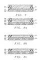
- FIGS. 1 a and 1 bshow conventional methods of creating wire bond connections to an Integrated Circuit die.
- FIG. 2is a cross-sectional drawing of the invention for a compliant metal to which a wire bond connection has been made.
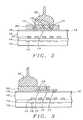
- FIG. 3shows a cross section of a second embodiment of the invention for compliant metal to which a wire bond connection has been made.
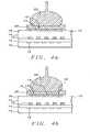
- FIG. 4 a and 4 bshow a cross sections of a third embodiment of invention showing compliant metal to which a wire bond connection has been made.
- FIGS. 5 a - 5 cshow cross sections of a fourth embodiment of the invention, for a compliant material over which a layer of pad metal has been created, a wire bond connection has been made to the layer of pad metal.
- FIG. 6shows a cross section of a fifth embodiment of the invention, for a compliant material over which a layer of pad metal has been created, a wire bond connection has been made to the layer of pad metal.
- FIG. 7shows a cross section of compliant metal.
- FIGS. 8 a through 8 cshow layers of material that can be used to form compliant metal.
- the inventionprovides a method which allows wire bonding connections to a semiconductor die to be made over active and/or passive devices, without damage to the devices or to intervening dielectric layers.
- wire bond connectionsare provided along the periphery of an Integrated Circuit (IC).
- ICIntegrated Circuit
- the bond padsare laterally displaced from the active device region in order to avoid the negative impact of mechanical stress that is introduced to and through underlying layers of dielectric during and as a result of wire bonding.
- FIG. 1 ahighlights a first region 70 in which active and/or passive devices are formed.
- the first region 70is separate from a second region 75 , over which bond pads 77 are formed.
- the top view shown in FIG. 1 ais shown in cross section in FIG. 1 b , wherein specifically are highlighted a substrate 71 , in or over the surface of which active and/or passive devices 72 have been created.
- a first layer 73 of interconnect metalis shown, which is typically connected at one or more points by contacts 74 , to devices 72 .
- One or more overlying layers 81 of interconnect metalare formed, in one or more layers of intermetal dielectric 76 , with a top metal layer from which bond pads 77 are formed.
- Bond pad 77 and wire bond 80are formed in second region 75 , and are laterally separated from above the first region 70 . As shown in FIGS. 1 a and 1 b , no active and/or passive devices are formed underlying the bond pad 77 .
- FIGS. 2-8 cThe invention will now be described in detail using FIGS. 2-8 c.
- the preferred method for the creation of wire bonding pad 20comprises the following steps:
- barrier layer metal etch7.
- the barrier layeris formed to a preferred thickness of about 3000 Angstroms, and is preferably formed of TiW (titanium tungsten).
- the seed layeris formed to a preferred thickness of about 1000 Angstroms and is preferably Au (gold).
- the photoresist used in step 3 . aboveis preferably formed to a thickness of between about 10 and 12 ⁇ m.
- Compliant metal 20is preferred to be created to a minimum thickness of about 1.0 ⁇ m, but is preferably more than 2 ⁇ m thick, and is preferably formed of Au. More generally, the thickness of the compliant metal should be based on the amount of energy the pad needs to absorb during wirebonding. The thicker the compliant metal pad thickness, the more energy the pad will be able to absorb.
- the small passivation openings 19 in FIGS. 2 and 3have a minimum cross section of about 0.1 ⁇ m, but are preferably at least 0.5 ⁇ m. Passivation openings 19 may be formed over only one of the contact pads 17 , but preferably some or all contact pads 17 under wirebond pad 20 have passivation openings formed thereover, as shown in FIG. 2 .
- the wire bonding region, to which wire bond 22 attachesis displaced laterally with respect to one or more of the openings 19 that has been provided through the passivation layer 18 . This allows for an offset of the wire bond 22 with respect to the passivation openings, providing additional flexibility in positioning the wire bond connection.
- FIG. 4 aanother embodiment is shown providing additional flexibility of providing wire bond connections to a semiconductor device, by providing a larger contact pad 17 .
- the layer 20 ′′ of compliant metalcontacts the top layer 17 of metal over a larger surface area, thus decreasing the interconnect series resistance of the bond pad/contact pad connection.
- the large passivation opening to contact pad 17shown in FIG. 4 a , has a width of between about 40 ⁇ m and 100 ⁇ m.
- FIG. 4 bYet another embodiment of the invention is shown in FIG. 4 b , in which a large contact pad 17 is used, but with multiple openings through the passivation layer 18 , which results in improved planarity of the top surface of bond pad 20 .
- the inventionprovides for, in another alternative embodiment as shown in FIG. 5 a , a layer 24 of a compliant post-passivation dielectric material, under compliant metal 26 .
- This compliant buffer layer 24is preferably an organic material such as polyimide, benzocyclobutene (BCB) or the like, and further assists in preventing damage to underlying dielectric layer(s) 16 and active/passive devices 12 .
- Other polymer materials that may be used for layer 24include elastomers such as silicone, or parylene.
- Compliant layer 24is typically deposited by spin-on techniques.
- Opening 23is created through the compliant post-passivation dielectric 24 , and extends to passivation opening 19 , providing access to top level contact point 17 .
- the openingmay have substantially vertical sidewalls 25 , however the sidewalls are preferably sloped as shown in FIG. 5 a .
- Compliant post-passivation dielectric 24such as polyimide, is spun on and exposed and developed to have vertical sidewalls, however the subsequent curing process causes the sidewalls to have the desired slope.
- the sidewall slope 25may have an angle ⁇ of 45 degrees or more, and is typically between about 50 and 60 degrees. It may be possible to form the sidewalls with an angle as small as 20 degrees.
- Layer 26is created to a preferred minimum thickness of about 1 ⁇ m, with gold the preferred material.
- the preferred method for the creation of the compliant buffer layer 24 of dielectricis spin coating, with layer 24 preferably created to a minimum thickness of about 2 ⁇ m.
- the preferred deposition processing steps for the creation of the buffer layer 24are the following:
- compliant buffer layer 24may be formed by screen printing, as is known in the art, a layer of polymer, such as polyimide or BCB, and then curing the layer.
- FIG. 5 bshows an alternative to the FIG. 5 a structure, in which multiple openings in the compliant dielectric layer 24 are formed, to connect wirebond pad 26 through multiple passivation openings 19 to multiple contact pads 17 .
- FIG. 5 cshows another alternative to the FIG. 5 a structure, in which multiple openings in the compliant dielectric layer 24 are formed, to connect wirebond pad 26 through multiple passivation openings 19 to a single, large contact pad 17 .
- the inventionprovides for offsetting the location of the wire bond 28 connection with respect to the connection(s) to contact pad(s) 17 .
- FIGS. 2 through 6have shown only two layers of overlying interconnect traces. It is clear that the invention is not limited to two layers of interconnect metal but can be equally applied with any number of such layers.
- the inventionis not limited to one opening created through a protective layer of passivation.
- the inventionis also not limited as to the location of the one or more openings that are created through the layer of passivation. What is critical to the invention is the application of a layer of compliant material, which serves as a buffer between active and/or passive devices and contact pads to which wire bond connections are to be provided.
- the off-set of the wire bond 22can be provided laterally in either direction with respect to the contact point 17 .
- the opening 19 through the layer 18 of passivationcan be extended to two or more openings, each of the openings providing access to points 17 of top level metal over the surface of the layer 16 of intermetal dielectric.
- FIGS. 2 and 3apply to the creation of small contact pads (compared to conventional bond pads) for which small vias are created through the layer 18 of passivation, while the cross section that is shown in FIG. 4 applies to the creation of a large contact pad for which a large via is created through the passivation layer 18 .
- FIGS. 7 and 8 a - 8 cadditional detail will be discussed with regard to materials and methods of forming the wirebond pad of the invention.
- Passivation layer 18is typically formed of an inorganic material. Typically, this comprises silicon oxide at about 0.5 ⁇ m thick over which is formed silicon nitride at about 0.7 ⁇ m thick. Other materials and thicknesses, as are known in the art, may be used.
- the passivation layerprotects underlying active and/or passive devices from the penetration of mobile ions, transition metals, moisture, and other contamination.
- a glue/barrier layer 29is deposited over passivation layer 18 .
- the glue/barrier layer 29preferably comprises Ti, Cr (chromium), TiW or TiN (titanium nitride).
- the preferred method for the creation of glue/barrier layer 29is sputtering.
- An electroplating seed layer 30is formed over the glue/barrier layer 29 , preferably by sputtering Au to a thickness of about 1000 Angstroms.
- Bondpad layer 32of electroplated soft Au, is formed over the seed layer, using a photolithographic process as earlier described.
- the Au bondpad layer 32shown in FIG. 7 , has the following characteristics:
- FIGS. 8 a through 8 cthree further embodiments of the invention are shown, in which a composite metal system is used to form the compliant metal pad.
- a glue/barrier layer 29is deposited over passivation layer 18 .
- Layer 29preferably comprises Ti or Cr, formed to a preferable thickness of about 500 Angstroms.
- a seed layer 33is formed over the barrier 29 , and preferably comprises sputtered Cu, formed to a preferable thickness of about 5000 Angstroms.
- a composite metal system 34 / 36 / 38is shown, preferably comprising electroplated Cu/Ni/Au, respectively.
- the bottom layer 34 of Cuforms a bulk conduction layer, and is preferred to have a thickness larger than about 1 ⁇ m.
- Center layer 36 of Niis used as a diffusion barrier, and is preferably formed to a thickness of between about 1 and 5 microns.
- the top Au layer 38is wire-bondable, and has a preferred thickness of at least 0.1 micron.
- the top wire bondable layermay be aluminum (Al).
- a two-metal systemis used.
- a first bulk conduction layer 34preferably comprising Cu, is formed over the seed layer 33 , and is preferably formed to a thickness of greater than about 1 micron.
- the second layer 38is formed over layer 34 , and preferably comprises Au of 0.1 micron, or Al.
- an electroplated solder 40is used as the bulk conduction metal, with Au (or Al) layer 38 used for wirebonding.
- the electroplated soldermay comprise Pb-alloy, Sn, Sn-alloy, or a lead-free solder such as AgSn alloy or AgCuSn alloy.
- a seed layer 33preferably comprises Cu or Ni.
- the compliant metal bond padsare formed as follows.
- a semiconductor wafer having top contact pads exposed through a layer of passivation 18is provided.
- the glue/barrier layer 29 and electroplating seed layer 33are deposited, typically by sputtering.
- the waferis coated with a layer of photoresist 31 having a thickness of less than 12 microns, with bond pad openings patterned by photolithography, as is known in the semiconductor art.
- Electroplatingis then performed for the various subsequent metal layers shown in these Figures, including the top wire-bondable layer 38 of gold. Alternatively, electroless plating may be used to form wire-bondable layer 38 to a thickness of as little as 100 Angstroms.
- a gold layer 32 with a thickness of less than 12 micronsmay be electroplated on the seed layer 30 exposed by the opening in the photoresist layer 31 , as shown in FIG. 7 .
- the photoresist 31is then stripped.
- the seed layer 33 and glue/barrier 29are etched using the bond pad as a mask, to complete the structure, which is now ready for wire bonding.
- additional composite layerssuch as a layer 34 (of Cu) or a layer 36 (of Ni) can be applied between layer 40 and the glue/barrier layer 29 .
- the Au layeris annealed at a temperature of between about 120° C. and 350° C., resulting in a hardness of between about 150 and 15 HV (the higher hardness corresponding to a lower annealing temperature, a lower hardness corresponding to a higher annealing temperature).
- a preferred annealing temperatureis about 270° C., which results in a hardness of about 50 Hv. Additionally, annealing may be performed in an N 2 ambient.
- the compliant layer 20may also be used to form low resistance power and ground planes, and/or for signal lines, above passivation layer 18 , as shown in U.S. Pat. No. 6,383,916, which is herein incorporated by reference.
- the metal pad of the inventionis referred to as “compliant”, as further described in the following.
- the compliant metal pad of the inventioncan be used to protect underlying active and/or passive devices and/or low-k dielectrics, from damage during wire bonding, because it serves as both a stress buffer (by its elasticity) and a shock wave absorber (by its ductility).
- a materialmust be soft, ductile (i.e., malleable), and sufficiently thick. Being soft (i.e., having high elasticity) is not sufficient to absorb much mechanical energy. It is the process of plastic deformation that determines how much mechanical energy a material can absorb. Further, the thicker the material, the greater is the energy that can be absorbed.
- Metalssuch as Au, Cu, solder and Al are all soft, for the purposes of the invention, but Au and solder are able to absorb more mechanical energy than Cu and Al due to their ductility.
- the total thickness of the compliant metal bond padsis preferred to be more than 1.5 um., in order to sufficiently absorb bonding energy.
- Low-k dielectric materialsthat could be used and protected from wire-bonding damage by the invention include CVD-deposited dielectrics including but not limited to polyarylene ether, polyarylene, polybenzoxazole, and spun-on dielectrics having a Si w C x O y H z composition. These low-k dielectrics generally have a dielectric constant less than 3.0, but are at least less than the dielectric contant of CVD-deposited SiO 2 , which has a dielectric constant of about 4.2.
- a key advantage of the inventionis the reduction in die size allowed by the placing of bond pads over the active devices, as compared to the traditional industry practice of laterally displacing the bonding regions from the active region. Further, due to the compliant nature of gold used in the bond pads of the invention, there are no restrictions on underlying interconnect metal routing.
- the compliant metal bond pad of the inventionadvantageously provides for absorption of the bonding force during wire bonding, thus preventing damage to active circuits and/or passive devices located underneath the bond pad.
- This absorption of the bonding forceis otherwise difficult to achieve by, for instance, conventional bond pad materials such as aluminum, which are very difficult to deposit and etch at thicknesses sufficient to absorb stress.
- the optional, additional organic layer of the inventionfurther helps in absorbing the force that is exerted during wire bonding.
- the inventionis particularly beneficial, by providing improved force absorption capabilities when compared with prior art methods, for deep-submicron technologies for which low-k dielectrics (which includes CVD or spun-on materials) are increasingly used.
Landscapes
- Engineering & Computer Science (AREA)
- Computer Hardware Design (AREA)
- Microelectronics & Electronic Packaging (AREA)
- Power Engineering (AREA)
- Manufacturing & Machinery (AREA)
- Internal Circuitry In Semiconductor Integrated Circuit Devices (AREA)
- Wire Bonding (AREA)
Abstract
Description
- This application is a continuation application of Ser. No. 10/434,142, filed on May 8, 2003, which claims priority to Provisional Patent Application Ser. No. 60/418,551, filed on Oct. 15, 2002, both of which are herein incorporated by reference in their entirety.
- This application is related to (MEG00-003), filed on May 7, 2001, Ser. No. 09/858,528, now issued as U.S. Pat. No. 6,593,649 and to (MEG02-009), filed on May 8, 2003, Ser. No. 10/434,524, both assigned (under a joint Assignment) to the Assignee of the instant invention.
- (1) Field of the Invention
- The invention relates to the fabrication of integrated circuit devices, and more particularly to the fabrication of wire bond pads over underlying active devices, passive devices and/or weak dielectric layers.
- (2) Background of the Invention
- Performance characteristics of semiconductor devices are typically improved by reducing device dimensions, resulting in increased device densities and increased device packaging densities. This increase in device density places increased requirements on the interconnection of semiconductor devices, which are addressed by the packaging of semiconductor devices. One of the key considerations in the package design is the accessibility of the semiconductor device or the Input/Output (I/O) capability of the package after one or more devices have been mounted in the package.
- In a typical semiconductor device package, the semiconductor die can be mounted or positioned in the package and can further be connected to interconnect lines of the substrate by bond wires or solder bumps. For this purpose the semiconductor die is provided with pads (bond pads) that are, typically mounted around the perimeter of the die, and are located such as not to be formed over regions containing active or passive devices.
- One reason the bond pads are not formed over the active or passive devices is related to the thermal and/or mechanical stresses that occur during the wire bonding process. During wirebonding, wires are connected from the bond pads to a supporting circuit board or to other means of interconnections.
- The semiconductor industry has recently turned increasingly to low dielectric-constant (or low-k) materials for intermetal dielectrics. However, such materials typically have lower mechanical strength than traditional insulating materials and are thus also susceptible to damage by wire bonding.
- U.S. Pat. No. 4,636,832 (Abe et al.) describes a method of forming a bond pad over an active area, using a silicon layer for stress reduction.
- U.S. Pat. No. 5,751,065 (Chittipeddi et al.) discloses a method of providing an integrated circuit with active devices under the bond pads, and uses metal for stress relief.
- U.S. Pat. No. 6,384,486 (Zuniga et al.) shows a method of forming an integrated circuit under a contact pad, also using a metal layer for stress absorption.
- U.S. Pat. No. 6,229,221 (Kloen et al.) describes forming a wire bond to a bond pad formed over active devices, where the bond pad and passivation must have specified thickness and be substantially free from interruptions under the wire bonding region.
- A principal objective of the invention is to provide a method and structure to enable wire bond connections over device regions of a semiconductor die, whereby damage to underlying layers of dielectric, active and/or passive devices is avoided.
- Another objective of the invention is to reduce semiconductor die size, and thus manufacturing cost, for integrated circuits to be connected to next level packaging by wire bonding.
- In accordance with the objectives of the invention, a new method and structure for enabling wire bond connections over active regions of an Integrated Circuit die is provided. A semiconductor die, on which are formed active and/or passive devices, has at least one interconnect metal layer having at least one top level metal contact, and a passivation layer over the interconnect metal layer, wherein the passivation layer comprises at least one opening through which is exposed the top level metal contact point. A compliant metal bond pad is formed over the passivation layer, connected to the top level metal contact through the opening.
- Various types, configurations or designs of openings through the layer of passivation are provided. Optionally, a layer of compliant material is formed between the compliant metal bond pad and passivation. Wire bonding may later be performed to the bond pad.
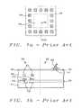
FIGS. 1 aand1bshow conventional methods of creating wire bond connections to an Integrated Circuit die.FIG. 2 is a cross-sectional drawing of the invention for a compliant metal to which a wire bond connection has been made.FIG. 3 shows a cross section of a second embodiment of the invention for compliant metal to which a wire bond connection has been made.FIG. 4 aand4bshow a cross sections of a third embodiment of invention showing compliant metal to which a wire bond connection has been made.FIGS. 5 a-5cshow cross sections of a fourth embodiment of the invention, for a compliant material over which a layer of pad metal has been created, a wire bond connection has been made to the layer of pad metal.FIG. 6 shows a cross section of a fifth embodiment of the invention, for a compliant material over which a layer of pad metal has been created, a wire bond connection has been made to the layer of pad metal.FIG. 7 shows a cross section of compliant metal.FIGS. 8 athrough8cshow layers of material that can be used to form compliant metal.- Conventional wire bonding methods and methods of I/O interconnect can result in damage being inflicted on underlying layers of dielectric, such as those layers of dielectric over which the interconnecting bond pads are formed. Furthermore, common industry practice has been to locate active devices away from the areas under bond pads, to avoid damage to the devices during wire bonding. This results in a significant increase in die size, causing extra manufacturing cost.
- The invention provides a method which allows wire bonding connections to a semiconductor die to be made over active and/or passive devices, without damage to the devices or to intervening dielectric layers.
- Conventional wire bond connections are provided along the periphery of an Integrated Circuit (IC). The bond pads are laterally displaced from the active device region in order to avoid the negative impact of mechanical stress that is introduced to and through underlying layers of dielectric during and as a result of wire bonding.
- This is illustrated using
FIGS. 1 aand1b, wherebyFIG. 1 ahighlights afirst region 70 in which active and/or passive devices are formed. Thefirst region 70 is separate from asecond region 75, over whichbond pads 77 are formed. The top view shown inFIG. 1 ais shown in cross section inFIG. 1 b, wherein specifically are highlighted asubstrate 71, in or over the surface of which active and/orpassive devices 72 have been created. Afirst layer 73 of interconnect metal is shown, which is typically connected at one or more points bycontacts 74, todevices 72. One or moreoverlying layers 81 of interconnect metal are formed, in one or more layers of intermetal dielectric76, with a top metal layer from whichbond pads 77 are formed.Bond pad 77 andwire bond 80 are formed insecond region 75, and are laterally separated from above thefirst region 70. As shown inFIGS. 1 aand1b, no active and/or passive devices are formed underlying thebond pad 77. - This requirement, of laterally separating
wire bonding pads 77 from underlying active and/orpassive devices 72 created in or over a semiconductor die, as highlighted inFIGS. 1 aand1b, causes the need for a significant increase in die size since thearea 70 is not available at the die top surface for wire bond connections. - The invention will now be described in detail using
FIGS. 2-8 c. - Referring first specifically to the cross section that is shown in
FIG. 2 , the following elements are shown: - 10, a substrate in or over which active semiconductor devices have been created (alternately, or in addition to, passive elements such as metal lines, capacitors, resistors, inductors and the like)
- 12, a representative sample of the semiconductor devices that have been created in or over
substrate 10; conductive points of electrical contact to devices12 (not shown) are provided - 14, a first layer of interlevel dielectric
- 15, metal interconnections in one or more layers
- 16, intermetal dielectric
- 17, contact pads formed from the top metal layer of interconnect metal
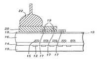
- 18, a layer of passivation deposited over the
layer 16 of intermetal dielectric andcontact pads 17 - 19, openings created through the
layer 18 of passivation for access to contactpads 17 - 20, of significant importance to the invention, a layer of compliant metal formed over
passivation layer 18 - 22, a wire bond connection provided to layer20 of complaint metal.
- The preferred method for the creation of
wire bonding pad 20 comprises the following steps: - 1. barrier layer sputtering
- 2. seed layer sputtering
- 3. a photo-lithographic process to define an opening for the bulk metal
- 4. electroplating the bulk metal
- 5. photoresist strip
- 6. seed layer metal etch
- 7. barrier layer metal etch.
- The barrier layer is formed to a preferred thickness of about 3000 Angstroms, and is preferably formed of TiW (titanium tungsten). The seed layer is formed to a preferred thickness of about 1000 Angstroms and is preferably Au (gold). The photoresist used in step3. above is preferably formed to a thickness of between about 10 and 12 μm.
Compliant metal 20 is preferred to be created to a minimum thickness of about 1.0 μm, but is preferably more than 2 μm thick, and is preferably formed of Au. More generally, the thickness of the compliant metal should be based on the amount of energy the pad needs to absorb during wirebonding. The thicker the compliant metal pad thickness, the more energy the pad will be able to absorb.- The
small passivation openings 19 inFIGS. 2 and 3 , have a minimum cross section of about 0.1 μm, but are preferably at least 0.5 μm.Passivation openings 19 may be formed over only one of thecontact pads 17, but preferably some or allcontact pads 17 underwirebond pad 20 have passivation openings formed thereover, as shown inFIG. 2 . - Referring now to
FIG. 3 , in an alternative embodiment the wire bonding region, to whichwire bond 22 attaches, is displaced laterally with respect to one or more of theopenings 19 that has been provided through thepassivation layer 18. This allows for an offset of thewire bond 22 with respect to the passivation openings, providing additional flexibility in positioning the wire bond connection. - With reference to
FIG. 4 a, another embodiment is shown providing additional flexibility of providing wire bond connections to a semiconductor device, by providing alarger contact pad 17. By creating alarge opening 19″ through thepassivation layer 18, thelayer 20″ of compliant metal contacts thetop layer 17 of metal over a larger surface area, thus decreasing the interconnect series resistance of the bond pad/contact pad connection. - The large passivation opening to contact
pad 17, shown inFIG. 4 a, has a width of between about 40 μm and 100 μm. - Yet another embodiment of the invention is shown in
FIG. 4 b, in which alarge contact pad 17 is used, but with multiple openings through thepassivation layer 18, which results in improved planarity of the top surface ofbond pad 20. - In order to further enhance absorption of bonding stresses, the invention provides for, in another alternative embodiment as shown in
FIG. 5 a, alayer 24 of a compliant post-passivation dielectric material, undercompliant metal 26. Thiscompliant buffer layer 24 is preferably an organic material such as polyimide, benzocyclobutene (BCB) or the like, and further assists in preventing damage to underlying dielectric layer(s)16 and active/passive devices 12. Other polymer materials that may be used forlayer 24 include elastomers such as silicone, or parylene.Compliant layer 24 is typically deposited by spin-on techniques. Opening 23 is created through thecompliant post-passivation dielectric 24, and extends to passivation opening19, providing access to toplevel contact point 17. The opening may have substantiallyvertical sidewalls 25, however the sidewalls are preferably sloped as shown inFIG. 5 a.Compliant post-passivation dielectric 24, such as polyimide, is spun on and exposed and developed to have vertical sidewalls, however the subsequent curing process causes the sidewalls to have the desired slope. Thesidewall slope 25 may have an angle α of 45 degrees or more, and is typically between about 50 and 60 degrees. It may be possible to form the sidewalls with an angle as small as 20 degrees.- As described earlier, the preferred method for the creation of
bond pad 26 is electroplating. Processing conditions applied for the embodiment ofFIG. 5 aare as follows: - 1. barrier layer metal sputtering
- 2. seed metal sputtering
- 3. photo-lithographic process
- 4. electroplating
- 5. photoresist strip
- 6. seed metal etching, and
- 7. barrier metal etching.
Layer 26 is created to a preferred minimum thickness of about 1 μm, with gold the preferred material.- The preferred method for the creation of the
compliant buffer layer 24 of dielectric is spin coating, withlayer 24 preferably created to a minimum thickness of about 2 μm. The preferred deposition processing steps for the creation of thebuffer layer 24 are the following: - 1. spin-coating of photo-sensitive material
- 2. photo lithographic exposure and development, and
- 3. curing.
- Alternately,
compliant buffer layer 24 may be formed by screen printing, as is known in the art, a layer of polymer, such as polyimide or BCB, and then curing the layer. FIG. 5 bshows an alternative to theFIG. 5 astructure, in which multiple openings in thecompliant dielectric layer 24 are formed, to connectwirebond pad 26 throughmultiple passivation openings 19 tomultiple contact pads 17.FIG. 5 cshows another alternative to theFIG. 5 astructure, in which multiple openings in thecompliant dielectric layer 24 are formed, to connectwirebond pad 26 throughmultiple passivation openings 19 to a single,large contact pad 17.- As yet a further extension, as shown in
FIG. 6 , the invention provides for offsetting the location of thewire bond 28 connection with respect to the connection(s) to contact pad(s)17. - It is clear that the invention lends itself to numerous variations in the application of the layer of compliant metal and compliant post-passivation dielectric material. The examples shown using
FIGS. 2 through 6 have shown only two layers of overlying interconnect traces. It is clear that the invention is not limited to two layers of interconnect metal but can be equally applied with any number of such layers. - As noted earlier, the invention is not limited to one opening created through a protective layer of passivation. The invention is also not limited as to the location of the one or more openings that are created through the layer of passivation. What is critical to the invention is the application of a layer of compliant material, which serves as a buffer between active and/or passive devices and contact pads to which wire bond connections are to be provided.
- Specifically and relating to the above comments it can be realized that, in the cross section shown in
FIG. 3 , the off-set of thewire bond 22 can be provided laterally in either direction with respect to thecontact point 17. Also and still specifically referring to the cross section ofFIG. 3 , theopening 19 through thelayer 18 of passivation can be extended to two or more openings, each of the openings providing access topoints 17 of top level metal over the surface of thelayer 16 of intermetal dielectric. - The cross sections that are shown in
FIGS. 2 and 3 apply to the creation of small contact pads (compared to conventional bond pads) for which small vias are created through thelayer 18 of passivation, while the cross section that is shown inFIG. 4 applies to the creation of a large contact pad for which a large via is created through thepassivation layer 18. - An experiment was performed in which the structure depicted in
FIG. 2 was formed, using 4 μm thick electroplated gold as thecompliant metal 20, and Fluorinated Silicate Glass (FSG) as theintermetal dielectric 16. After wire bonding, no damage to the intermetal dielectric was observed. - Referring now to
FIGS. 7 and 8 a-8c, additional detail will be discussed with regard to materials and methods of forming the wirebond pad of the invention. Passivation layer 18 is typically formed of an inorganic material. Typically, this comprises silicon oxide at about 0.5 μm thick over which is formed silicon nitride at about 0.7 μm thick. Other materials and thicknesses, as are known in the art, may be used. The passivation layer protects underlying active and/or passive devices from the penetration of mobile ions, transition metals, moisture, and other contamination.- In one embodiment of the invention, as shown in
FIG. 7 , a glue/barrier layer 29 is deposited overpassivation layer 18. The glue/barrier layer 29 preferably comprises Ti, Cr (chromium), TiW or TiN (titanium nitride). The preferred method for the creation of glue/barrier layer 29 is sputtering. - An
electroplating seed layer 30 is formed over the glue/barrier layer 29, preferably by sputtering Au to a thickness of about 1000 Angstroms. Bondpad layer 32, of electroplated soft Au, is formed over the seed layer, using a photolithographic process as earlier described.- The
Au bondpad layer 32, shown inFIG. 7 , has the following characteristics: - a hardness range of less than about 150 Hv (Vickers Hardness), whereby softer Au is preferred, since softer Au is better suited for stress absorption during wire bond formation
- an Au purity larger than about 97%, and
- a thickness larger than about 1 μm, since a thickness less than about 1 μm does not provide adequate stress absorption.
- Referring now to
FIGS. 8 athrough8c, three further embodiments of the invention are shown, in which a composite metal system is used to form the compliant metal pad. - In all three embodiments, a glue/
barrier layer 29 is deposited overpassivation layer 18.Layer 29 preferably comprises Ti or Cr, formed to a preferable thickness of about 500 Angstroms. Aseed layer 33 is formed over thebarrier 29, and preferably comprises sputtered Cu, formed to a preferable thickness of about 5000 Angstroms. - Referring now specifically to
FIG. 8 a, acomposite metal system 34/36/38 is shown, preferably comprising electroplated Cu/Ni/Au, respectively. Thebottom layer 34 of Cu forms a bulk conduction layer, and is preferred to have a thickness larger than about 1 μm. Center layer36 of Ni is used as a diffusion barrier, and is preferably formed to a thickness of between about 1 and 5 microns. Thetop Au layer 38, is wire-bondable, and has a preferred thickness of at least 0.1 micron. Alternately, the top wire bondable layer may be aluminum (Al). - In the next embodiment, as shown in
FIG. 8 b, a two-metal system is used. A firstbulk conduction layer 34, preferably comprising Cu, is formed over theseed layer 33, and is preferably formed to a thickness of greater than about 1 micron. Thesecond layer 38, for wire bonding purposes, is formed overlayer 34, and preferably comprises Au of 0.1 micron, or Al. - In the embodiment shown in
FIG. 8 c, an electroplatedsolder 40 is used as the bulk conduction metal, with Au (or Al)layer 38 used for wirebonding. The electroplated solder may comprise Pb-alloy, Sn, Sn-alloy, or a lead-free solder such as AgSn alloy or AgCuSn alloy. Aseed layer 33 preferably comprises Cu or Ni. - In the above embodiments of
FIGS. 7 and 8 a-8c, the compliant metal bond pads are formed as follows. A semiconductor wafer having top contact pads exposed through a layer ofpassivation 18 is provided. The glue/barrier layer 29 andelectroplating seed layer 33 are deposited, typically by sputtering. Next, the wafer is coated with a layer ofphotoresist 31 having a thickness of less than 12 microns, with bond pad openings patterned by photolithography, as is known in the semiconductor art. Electroplating is then performed for the various subsequent metal layers shown in these Figures, including the top wire-bondable layer 38 of gold. Alternatively, electroless plating may be used to form wire-bondable layer 38 to a thickness of as little as 100 Angstroms. Agold layer 32 with a thickness of less than 12 microns may be electroplated on theseed layer 30 exposed by the opening in thephotoresist layer 31, as shown inFIG. 7 . Thephotoresist 31 is then stripped. Theseed layer 33 and glue/barrier 29 are etched using the bond pad as a mask, to complete the structure, which is now ready for wire bonding. - For the layers shown in cross section in
FIGS. 8 a-8c, the Following preferred thicknesses apply: - the layer of
Cu 34 is preferred to have a thickness larger than about 1 μm - the diffusion layer36 of Ni is preferred to have a thickness larger than about 0.5 μm
- the
wirebondable Au layer 38 is preferred to have a thickness larger than about 100 Angstroms - the layer of Pb-alloy, sn or Sn-
alloy 40 is preferred to have a thickness larger than about 1 μm.
- the layer of
- Further, with the layer of Pb-alloy, Sn or Sn-alloy, as shown in the cross section of
FIG. 8 c, additional composite layers such as a layer34 (of Cu) or a layer36 (of Ni) can be applied betweenlayer 40 and the glue/barrier layer 29. - To adjust the hardness of the Au layer, the Au layer is annealed at a temperature of between about 120° C. and 350° C., resulting in a hardness of between about 150 and 15 HV (the higher hardness corresponding to a lower annealing temperature, a lower hardness corresponding to a higher annealing temperature). A preferred annealing temperature is about 270° C., which results in a hardness of about 50 Hv. Additionally, annealing may be performed in an N2ambient.
- The
compliant layer 20, as shown in the cross section ofFIG. 1 , may also be used to form low resistance power and ground planes, and/or for signal lines, abovepassivation layer 18, as shown in U.S. Pat. No. 6,383,916, which is herein incorporated by reference. - The metal pad of the invention is referred to as “compliant”, as further described in the following. The compliant metal pad of the invention can be used to protect underlying active and/or passive devices and/or low-k dielectrics, from damage during wire bonding, because it serves as both a stress buffer (by its elasticity) and a shock wave absorber (by its ductility). To absorb mechanical energy, a material must be soft, ductile (i.e., malleable), and sufficiently thick. Being soft (i.e., having high elasticity) is not sufficient to absorb much mechanical energy. It is the process of plastic deformation that determines how much mechanical energy a material can absorb. Further, the thicker the material, the greater is the energy that can be absorbed. Metals such as Au, Cu, solder and Al are all soft, for the purposes of the invention, but Au and solder are able to absorb more mechanical energy than Cu and Al due to their ductility.
- The total thickness of the compliant metal bond pads is preferred to be more than 1.5 um., in order to sufficiently absorb bonding energy.
- Low-k dielectric materials that could be used and protected from wire-bonding damage by the invention include CVD-deposited dielectrics including but not limited to polyarylene ether, polyarylene, polybenzoxazole, and spun-on dielectrics having a SiwCxOyHzcomposition. These low-k dielectrics generally have a dielectric constant less than 3.0, but are at least less than the dielectric contant of CVD-deposited SiO2, which has a dielectric constant of about 4.2.
- A key advantage of the invention is the reduction in die size allowed by the placing of bond pads over the active devices, as compared to the traditional industry practice of laterally displacing the bonding regions from the active region. Further, due to the compliant nature of gold used in the bond pads of the invention, there are no restrictions on underlying interconnect metal routing.
- The compliant metal bond pad of the invention advantageously provides for absorption of the bonding force during wire bonding, thus preventing damage to active circuits and/or passive devices located underneath the bond pad. This absorption of the bonding force is otherwise difficult to achieve by, for instance, conventional bond pad materials such as aluminum, which are very difficult to deposit and etch at thicknesses sufficient to absorb stress.
- The optional, additional organic layer of the invention further helps in absorbing the force that is exerted during wire bonding.
- The invention is particularly beneficial, by providing improved force absorption capabilities when compared with prior art methods, for deep-submicron technologies for which low-k dielectrics (which includes CVD or spun-on materials) are increasingly used.
- Although the invention has been described and illustrated with reference to specific illustrative embodiments thereof, it is not intended that the invention be limited to those illustrative embodiments. Those skilled in the art will recognize that variations and modifications can be made without departing from the spirit of the invention. It is therefore intended to include within the invention all such variations and modifications which fall within the scope of the appended claims and equivalents thereof.
Claims (38)
Priority Applications (1)
| Application Number | Priority Date | Filing Date | Title |
|---|---|---|---|
| US11/678,599US9153555B2 (en) | 2002-10-15 | 2007-02-25 | Method of wire bonding over active area of a semiconductor circuit |
Applications Claiming Priority (3)
| Application Number | Priority Date | Filing Date | Title |
|---|---|---|---|
| US41855102P | 2002-10-15 | 2002-10-15 | |
| US10/434,142US8021976B2 (en) | 2002-10-15 | 2003-05-08 | Method of wire bonding over active area of a semiconductor circuit |
| US11/678,599US9153555B2 (en) | 2002-10-15 | 2007-02-25 | Method of wire bonding over active area of a semiconductor circuit |
Related Parent Applications (1)
| Application Number | Title | Priority Date | Filing Date |
|---|---|---|---|
| US10/434,142ContinuationUS8021976B2 (en) | 1998-12-21 | 2003-05-08 | Method of wire bonding over active area of a semiconductor circuit |
Publications (2)
| Publication Number | Publication Date |
|---|---|
| US20070164453A1true US20070164453A1 (en) | 2007-07-19 |
| US9153555B2 US9153555B2 (en) | 2015-10-06 |
Family
ID=46204822
Family Applications (8)
| Application Number | Title | Priority Date | Filing Date |
|---|---|---|---|
| US10/434,142Expired - Fee RelatedUS8021976B2 (en) | 1998-12-21 | 2003-05-08 | Method of wire bonding over active area of a semiconductor circuit |
| US11/707,827Expired - Fee RelatedUS8026588B2 (en) | 2002-10-15 | 2007-02-16 | Method of wire bonding over active area of a semiconductor circuit |
| US11/678,600Expired - LifetimeUS8742580B2 (en) | 2002-10-15 | 2007-02-25 | Method of wire bonding over active area of a semiconductor circuit |
| US11/678,599Expired - LifetimeUS9153555B2 (en) | 2002-10-15 | 2007-02-25 | Method of wire bonding over active area of a semiconductor circuit |
| US11/678,598Expired - Fee RelatedUS7521812B2 (en) | 2002-10-15 | 2007-02-25 | Method of wire bonding over active area of a semiconductor circuit |
| US11/678,597AbandonedUS20070164412A1 (en) | 2002-10-15 | 2007-02-25 | Method of wire bonding over active area of a semiconductor circuit |
| US11/926,154Expired - Fee RelatedUS8138079B2 (en) | 1998-12-21 | 2007-10-29 | Method of wire bonding over active area of a semiconductor circuit |
| US11/926,156Expired - Fee RelatedUS9142527B2 (en) | 2002-10-15 | 2007-10-29 | Method of wire bonding over active area of a semiconductor circuit |
Family Applications Before (3)
| Application Number | Title | Priority Date | Filing Date |
|---|---|---|---|
| US10/434,142Expired - Fee RelatedUS8021976B2 (en) | 1998-12-21 | 2003-05-08 | Method of wire bonding over active area of a semiconductor circuit |
| US11/707,827Expired - Fee RelatedUS8026588B2 (en) | 2002-10-15 | 2007-02-16 | Method of wire bonding over active area of a semiconductor circuit |
| US11/678,600Expired - LifetimeUS8742580B2 (en) | 2002-10-15 | 2007-02-25 | Method of wire bonding over active area of a semiconductor circuit |
Family Applications After (4)
| Application Number | Title | Priority Date | Filing Date |
|---|---|---|---|
| US11/678,598Expired - Fee RelatedUS7521812B2 (en) | 2002-10-15 | 2007-02-25 | Method of wire bonding over active area of a semiconductor circuit |
| US11/678,597AbandonedUS20070164412A1 (en) | 2002-10-15 | 2007-02-25 | Method of wire bonding over active area of a semiconductor circuit |
| US11/926,154Expired - Fee RelatedUS8138079B2 (en) | 1998-12-21 | 2007-10-29 | Method of wire bonding over active area of a semiconductor circuit |
| US11/926,156Expired - Fee RelatedUS9142527B2 (en) | 2002-10-15 | 2007-10-29 | Method of wire bonding over active area of a semiconductor circuit |
Country Status (1)
| Country | Link |
|---|---|
| US (8) | US8021976B2 (en) |
Cited By (4)
| Publication number | Priority date | Publication date | Assignee | Title |
|---|---|---|---|---|
| US20080045003A1 (en)* | 2002-10-15 | 2008-02-21 | Megica Corporation | Method of wire bonding over active area of a semiconductor circuit |
| US7420280B1 (en)* | 2005-05-02 | 2008-09-02 | National Semiconductor Corporation | Reduced stress under bump metallization structure |
| CN104299952A (en)* | 2013-07-16 | 2015-01-21 | 台湾积体电路制造股份有限公司 | Mechanisms for forming bump structures over wide metal pad |
| DE102014217985A1 (en)* | 2014-09-09 | 2016-03-10 | Robert Bosch Gmbh | Method for producing a bond pad, bond pad and bonding method |
Families Citing this family (153)
| Publication number | Priority date | Publication date | Assignee | Title |
|---|---|---|---|---|
| US6869870B2 (en) | 1998-12-21 | 2005-03-22 | Megic Corporation | High performance system-on-chip discrete components using post passivation process |
| US7381642B2 (en)* | 2004-09-23 | 2008-06-03 | Megica Corporation | Top layers of metal for integrated circuits |
| US7288845B2 (en)* | 2002-10-15 | 2007-10-30 | Marvell Semiconductor, Inc. | Fabrication of wire bond pads over underlying active devices, passive devices and/or dielectric layers in integrated circuits |
| JP4170103B2 (en)* | 2003-01-30 | 2008-10-22 | Necエレクトロニクス株式会社 | Semiconductor device and manufacturing method of semiconductor device |
| US7319277B2 (en)* | 2003-05-08 | 2008-01-15 | Megica Corporation | Chip structure with redistribution traces |
| US8274160B2 (en) | 2003-08-21 | 2012-09-25 | Intersil Americas Inc. | Active area bonding compatible high current structures |
| US7005369B2 (en)* | 2003-08-21 | 2006-02-28 | Intersil American Inc. | Active area bonding compatible high current structures |
| US7459790B2 (en) | 2003-10-15 | 2008-12-02 | Megica Corporation | Post passivation interconnection schemes on top of the IC chips |
| JP2005347622A (en)* | 2004-06-04 | 2005-12-15 | Seiko Epson Corp | Semiconductor device, circuit board and electronic equipment |
| US7465654B2 (en) | 2004-07-09 | 2008-12-16 | Megica Corporation | Structure of gold bumps and gold conductors on one IC die and methods of manufacturing the structures |
| US8022544B2 (en) | 2004-07-09 | 2011-09-20 | Megica Corporation | Chip structure |
| TWI283443B (en) | 2004-07-16 | 2007-07-01 | Megica Corp | Post-passivation process and process of forming a polymer layer on the chip |
| US7226857B2 (en) | 2004-07-30 | 2007-06-05 | Micron Technology, Inc. | Front-end processing of nickel plated bond pads |
| US7452803B2 (en) | 2004-08-12 | 2008-11-18 | Megica Corporation | Method for fabricating chip structure |
| US7521805B2 (en)* | 2004-10-12 | 2009-04-21 | Megica Corp. | Post passivation interconnection schemes on top of the IC chips |
| US7547969B2 (en) | 2004-10-29 | 2009-06-16 | Megica Corporation | Semiconductor chip with passivation layer comprising metal interconnect and contact pads |
| US7361581B2 (en)* | 2004-11-23 | 2008-04-22 | International Business Machines Corporation | High surface area aluminum bond pad for through-wafer connections to an electronic package |
| JP4606145B2 (en)* | 2004-12-09 | 2011-01-05 | セイコーエプソン株式会社 | Semiconductor device and manufacturing method thereof |
| US7586199B1 (en) | 2005-03-23 | 2009-09-08 | Marvell International Ltd. | Structures, architectures, systems, methods, algorithms and software for configuring and integrated circuit for multiple packaging types |
| US8405220B1 (en)* | 2005-03-23 | 2013-03-26 | Marvell International Ltd. | Structures, architectures, systems, methods, algorithms and software for configuring an integrated circuit for multiple packaging types |
| US7157734B2 (en)* | 2005-05-27 | 2007-01-02 | Taiwan Semiconductor Manufacturing Company, Ltd. | Semiconductor bond pad structures and methods of manufacturing thereof |
| US7364998B2 (en)* | 2005-07-21 | 2008-04-29 | Taiwan Semiconductor Manufacturing Co., Ltd. | Method for forming high reliability bump structure |
| CN1901162B (en) | 2005-07-22 | 2011-04-20 | 米辑电子股份有限公司 | Method for manufacturing circuit assembly by continuous electroplating and circuit assembly structure |
| US8399989B2 (en)* | 2005-07-29 | 2013-03-19 | Megica Corporation | Metal pad or metal bump over pad exposed by passivation layer |
| US8148822B2 (en)* | 2005-07-29 | 2012-04-03 | Megica Corporation | Bonding pad on IC substrate and method for making the same |
| JP4671814B2 (en)* | 2005-09-02 | 2011-04-20 | パナソニック株式会社 | Semiconductor device |
| US7646097B2 (en)* | 2005-10-11 | 2010-01-12 | Taiwan Semiconductor Manufacturing Co., Ltd. | Bond pads and methods for fabricating the same |
| US7397121B2 (en)* | 2005-10-28 | 2008-07-08 | Megica Corporation | Semiconductor chip with post-passivation scheme formed over passivation layer |
| US7385297B1 (en)* | 2005-11-14 | 2008-06-10 | National Semiconductor Corporation | Under-bond pad structures for integrated circuit devices |
| US8836146B2 (en)* | 2006-03-02 | 2014-09-16 | Qualcomm Incorporated | Chip package and method for fabricating the same |
| US7592710B2 (en)* | 2006-03-03 | 2009-09-22 | Taiwan Semiconductor Manufacturing Company, Ltd. | Bond pad structure for wire bonding |
| US8344524B2 (en)* | 2006-03-07 | 2013-01-01 | Megica Corporation | Wire bonding method for preventing polymer cracking |
| US8420520B2 (en)* | 2006-05-18 | 2013-04-16 | Megica Corporation | Non-cyanide gold electroplating for fine-line gold traces and gold pads |
| TWI306298B (en)* | 2006-07-17 | 2009-02-11 | Chipmos Technologies Inc | Chip structure |
| GB0616125D0 (en)* | 2006-08-14 | 2006-09-20 | Radiation Watch Ltd | Etch process |
| US7960825B2 (en)* | 2006-09-06 | 2011-06-14 | Megica Corporation | Chip package and method for fabricating the same |
| US7582966B2 (en) | 2006-09-06 | 2009-09-01 | Megica Corporation | Semiconductor chip and method for fabricating the same |
| US7749885B2 (en)* | 2006-12-15 | 2010-07-06 | Micron Technology, Inc. | Semiconductor processing methods, methods of forming contact pads, and methods of forming electrical connections between metal-containing layers |
| US8377044B2 (en) | 2007-03-30 | 2013-02-19 | Ethicon Endo-Surgery, Inc. | Detachable end effectors |
| US20080284009A1 (en)* | 2007-05-16 | 2008-11-20 | Heikyung Min | Dimple free gold bump for drive IC |
| US8030733B1 (en) | 2007-05-22 | 2011-10-04 | National Semiconductor Corporation | Copper-compatible fuse target |
| US7964934B1 (en) | 2007-05-22 | 2011-06-21 | National Semiconductor Corporation | Fuse target and method of forming the fuse target in a copper process flow |
| SG149807A1 (en) | 2007-07-30 | 2009-02-27 | Stats Chippac Ltd | Semiconductor device and method of providing common voltage bus and wire bondable redistribution |
| US7906424B2 (en)* | 2007-08-01 | 2011-03-15 | Advanced Micro Devices, Inc. | Conductor bump method and apparatus |
| DE102007037858B4 (en) | 2007-08-10 | 2012-04-19 | Infineon Technologies Ag | Semiconductor device with improved dynamic behavior |
| US8030775B2 (en) | 2007-08-27 | 2011-10-04 | Megica Corporation | Wirebond over post passivation thick metal |
| US7888257B2 (en)* | 2007-10-10 | 2011-02-15 | Agere Systems Inc. | Integrated circuit package including wire bonds |
| JP2011502352A (en)* | 2007-10-31 | 2011-01-20 | アギア システムズ インコーポレーテッド | Bond pad support structure for semiconductor devices |
| WO2009122314A1 (en)* | 2008-03-31 | 2009-10-08 | Nxp B.V. | A sensor chip and a method of manufacturing the same |
| US8314474B2 (en)* | 2008-07-25 | 2012-11-20 | Ati Technologies Ulc | Under bump metallization for on-die capacitor |
| US7709956B2 (en)* | 2008-09-15 | 2010-05-04 | National Semiconductor Corporation | Copper-topped interconnect structure that has thin and thick copper traces and method of forming the copper-topped interconnect structure |
| US8088634B2 (en) | 2008-11-11 | 2012-01-03 | Johnson Morgan T | Methods of adding pads and one or more interconnect layers to the passivated topside of a wafer including connections to at least a portion of the integrated circuit pads thereon |
| US8581423B2 (en) | 2008-11-17 | 2013-11-12 | Taiwan Semiconductor Manufacturing Company, Ltd. | Double solid metal pad with reduced area |
| US8357998B2 (en)* | 2009-02-09 | 2013-01-22 | Advanced Semiconductor Engineering, Inc. | Wirebonded semiconductor package |
| JP5249080B2 (en)* | 2009-02-19 | 2013-07-31 | セイコーインスツル株式会社 | Semiconductor device |
| US8026608B2 (en)* | 2009-03-24 | 2011-09-27 | General Electric Company | Stackable electronic package |
| US8153510B2 (en)* | 2009-05-01 | 2012-04-10 | Power Gold LLC | Semiconductor bond pad patterns and method of formation |
| US8955215B2 (en) | 2009-05-28 | 2015-02-17 | Hsio Technologies, Llc | High performance surface mount electrical interconnect |
| US9536815B2 (en) | 2009-05-28 | 2017-01-03 | Hsio Technologies, Llc | Semiconductor socket with direct selective metalization |
| US9276336B2 (en) | 2009-05-28 | 2016-03-01 | Hsio Technologies, Llc | Metalized pad to electrical contact interface |
| WO2011153298A1 (en) | 2010-06-03 | 2011-12-08 | Hsio Technologies, Llc | Electrical connector insulator housing |
| WO2010147939A1 (en) | 2009-06-17 | 2010-12-23 | Hsio Technologies, Llc | Semiconductor socket |
| WO2010141296A1 (en) | 2009-06-02 | 2010-12-09 | Hsio Technologies, Llc | Compliant printed circuit semiconductor package |
| US9232654B2 (en) | 2009-06-02 | 2016-01-05 | Hsio Technologies, Llc | High performance electrical circuit structure |
| US9196980B2 (en) | 2009-06-02 | 2015-11-24 | Hsio Technologies, Llc | High performance surface mount electrical interconnect with external biased normal force loading |
| WO2010141313A1 (en) | 2009-06-02 | 2010-12-09 | Hsio Technologies, Llc | Compliant printed circuit socket diagnostic tool |
| US8987886B2 (en) | 2009-06-02 | 2015-03-24 | Hsio Technologies, Llc | Copper pillar full metal via electrical circuit structure |
| US9318862B2 (en) | 2009-06-02 | 2016-04-19 | Hsio Technologies, Llc | Method of making an electronic interconnect |
| US9613841B2 (en) | 2009-06-02 | 2017-04-04 | Hsio Technologies, Llc | Area array semiconductor device package interconnect structure with optional package-to-package or flexible circuit to package connection |
| US9603249B2 (en) | 2009-06-02 | 2017-03-21 | Hsio Technologies, Llc | Direct metalization of electrical circuit structures |
| US8988093B2 (en) | 2009-06-02 | 2015-03-24 | Hsio Technologies, Llc | Bumped semiconductor wafer or die level electrical interconnect |
| US9054097B2 (en) | 2009-06-02 | 2015-06-09 | Hsio Technologies, Llc | Compliant printed circuit area array semiconductor device package |
| US9136196B2 (en) | 2009-06-02 | 2015-09-15 | Hsio Technologies, Llc | Compliant printed circuit wafer level semiconductor package |
| US9699906B2 (en) | 2009-06-02 | 2017-07-04 | Hsio Technologies, Llc | Hybrid printed circuit assembly with low density main core and embedded high density circuit regions |
| US8525346B2 (en) | 2009-06-02 | 2013-09-03 | Hsio Technologies, Llc | Compliant conductive nano-particle electrical interconnect |
| WO2012074963A1 (en) | 2010-12-01 | 2012-06-07 | Hsio Technologies, Llc | High performance surface mount electrical interconnect |
| WO2010141264A1 (en) | 2009-06-03 | 2010-12-09 | Hsio Technologies, Llc | Compliant wafer level probe assembly |
| US9414500B2 (en) | 2009-06-02 | 2016-08-09 | Hsio Technologies, Llc | Compliant printed flexible circuit |
| US9930775B2 (en) | 2009-06-02 | 2018-03-27 | Hsio Technologies, Llc | Copper pillar full metal via electrical circuit structure |
| WO2011002709A1 (en) | 2009-06-29 | 2011-01-06 | Hsio Technologies, Llc | Compliant printed circuit semiconductor tester interface |
| US8955216B2 (en) | 2009-06-02 | 2015-02-17 | Hsio Technologies, Llc | Method of making a compliant printed circuit peripheral lead semiconductor package |
| US9276339B2 (en) | 2009-06-02 | 2016-03-01 | Hsio Technologies, Llc | Electrical interconnect IC device socket |
| US9231328B2 (en) | 2009-06-02 | 2016-01-05 | Hsio Technologies, Llc | Resilient conductive electrical interconnect |
| US9184145B2 (en) | 2009-06-02 | 2015-11-10 | Hsio Technologies, Llc | Semiconductor device package adapter |
| WO2010147934A1 (en) | 2009-06-16 | 2010-12-23 | Hsio Technologies, Llc | Semiconductor die terminal |
| US8610265B2 (en) | 2009-06-02 | 2013-12-17 | Hsio Technologies, Llc | Compliant core peripheral lead semiconductor test socket |
| WO2010141298A1 (en) | 2009-06-02 | 2010-12-09 | Hsio Technologies, Llc | Composite polymer-metal electrical contacts |
| WO2010141318A1 (en) | 2009-06-02 | 2010-12-09 | Hsio Technologies, Llc | Compliant printed circuit peripheral lead semiconductor test socket |
| US9320133B2 (en) | 2009-06-02 | 2016-04-19 | Hsio Technologies, Llc | Electrical interconnect IC device socket |
| US8912812B2 (en) | 2009-06-02 | 2014-12-16 | Hsio Technologies, Llc | Compliant printed circuit wafer probe diagnostic tool |
| WO2010147782A1 (en) | 2009-06-16 | 2010-12-23 | Hsio Technologies, Llc | Simulated wirebond semiconductor package |
| US8984748B2 (en) | 2009-06-29 | 2015-03-24 | Hsio Technologies, Llc | Singulated semiconductor device separable electrical interconnect |
| US8436251B2 (en)* | 2009-07-08 | 2013-05-07 | Medtronic, Inc. | Ribbon connecting electrical components |
| DE102009035437B4 (en)* | 2009-07-31 | 2012-09-27 | Globalfoundries Dresden Module One Llc & Co. Kg | A semiconductor device having a stress buffering material formed over a low ε metallization system |
| EP2478555A1 (en)* | 2009-09-17 | 2012-07-25 | Koninklijke Philips Electronics N.V. | Geometry of contact sites at brittle inorganic layers in electronic devices |
| JP5497392B2 (en)* | 2009-09-25 | 2014-05-21 | ルネサスエレクトロニクス株式会社 | Semiconductor device |
| US9295485B2 (en) | 2009-10-09 | 2016-03-29 | Ethicon Endo-Surgery, Inc. | Loader for exchanging end effectors in vivo |
| US9186203B2 (en)* | 2009-10-09 | 2015-11-17 | Ethicon Endo-Surgery, Inc. | Method for exchanging end effectors In Vivo |
| US20110087265A1 (en)* | 2009-10-09 | 2011-04-14 | Nobis Rudolph H | Laparoscopic instrument with attachable end effector |
| US8492896B2 (en)* | 2010-05-21 | 2013-07-23 | Panasonic Corporation | Semiconductor apparatus and semiconductor apparatus unit |
| US8901736B2 (en) | 2010-05-28 | 2014-12-02 | Taiwan Semiconductor Manufacturing Company, Ltd. | Strength of micro-bump joints |
| US8758067B2 (en) | 2010-06-03 | 2014-06-24 | Hsio Technologies, Llc | Selective metalization of electrical connector or socket housing |
| US9350093B2 (en) | 2010-06-03 | 2016-05-24 | Hsio Technologies, Llc | Selective metalization of electrical connector or socket housing |
| US9689897B2 (en) | 2010-06-03 | 2017-06-27 | Hsio Technologies, Llc | Performance enhanced semiconductor socket |
| US10159154B2 (en) | 2010-06-03 | 2018-12-18 | Hsio Technologies, Llc | Fusion bonded liquid crystal polymer circuit structure |
| GB2482894B (en)* | 2010-08-18 | 2014-11-12 | Cambridge Silicon Radio Ltd | Interconnection structure |
| US8802554B2 (en)* | 2011-02-15 | 2014-08-12 | Marvell World Trade Ltd. | Patterns of passivation material on bond pads and methods of manufacture thereof |
| US8409979B2 (en)* | 2011-05-31 | 2013-04-02 | Stats Chippac, Ltd. | Semiconductor device and method of forming interconnect structure with conductive pads having expanded interconnect surface area for enhanced interconnection properties |
| US8994181B2 (en)* | 2011-08-18 | 2015-03-31 | Taiwan Semiconductor Manufacturing Company, Ltd. | Bond pad structure to reduce bond pad corrosion |
| US8618677B2 (en) | 2012-04-06 | 2013-12-31 | Advanced Semiconductor Engineering, Inc. | Wirebonded semiconductor package |
| US9761520B2 (en) | 2012-07-10 | 2017-09-12 | Hsio Technologies, Llc | Method of making an electrical connector having electrodeposited terminals |
| US8710607B2 (en) | 2012-07-12 | 2014-04-29 | Taiwan Semiconductor Manufacturing Company, Ltd. | Method and apparatus for image sensor packaging |
| JP5919128B2 (en)* | 2012-08-03 | 2016-05-18 | ルネサスエレクトロニクス株式会社 | Semiconductor device and manufacturing method thereof |
| US9125681B2 (en) | 2012-09-26 | 2015-09-08 | Ethicon Endo-Surgery, Inc. | Detachable end effector and loader |
| US9398905B2 (en) | 2012-12-13 | 2016-07-26 | Ethicon Endo-Surgery, Llc | Circular needle applier with offset needle and carrier tracks |
| US9451937B2 (en) | 2013-02-27 | 2016-09-27 | Ethicon Endo-Surgery, Llc | Percutaneous instrument with collet locking mechanisms |
| NO2944700T3 (en) | 2013-07-11 | 2018-03-17 | ||
| US10667410B2 (en) | 2013-07-11 | 2020-05-26 | Hsio Technologies, Llc | Method of making a fusion bonded circuit structure |
| US10506722B2 (en) | 2013-07-11 | 2019-12-10 | Hsio Technologies, Llc | Fusion bonded liquid crystal polymer electrical circuit structure |
| US20150123267A1 (en)* | 2013-11-06 | 2015-05-07 | Taiwan Semiconductor Manufacturing Company Ltd. | Packaged semiconductor device |
| WO2015132924A1 (en)* | 2014-03-06 | 2015-09-11 | 三菱電機株式会社 | Semiconductor device |
| KR102284123B1 (en)* | 2014-05-26 | 2021-07-30 | 삼성전기주식회사 | Circuit board, electronic component and method of manufacturing circuit board |
| KR102245825B1 (en) | 2014-09-04 | 2021-04-30 | 삼성전자주식회사 | Semiconductor pakage |
| US9960130B2 (en)* | 2015-02-06 | 2018-05-01 | UTAC Headquarters Pte. Ltd. | Reliable interconnect |
| US9559447B2 (en) | 2015-03-18 | 2017-01-31 | Hsio Technologies, Llc | Mechanical contact retention within an electrical connector |
| US10342520B2 (en) | 2015-08-26 | 2019-07-09 | Ethicon Llc | Articulating surgical devices and loaders having stabilizing features |
| US10335196B2 (en) | 2015-08-31 | 2019-07-02 | Ethicon Llc | Surgical instrument having a stop guard |
| US10251636B2 (en) | 2015-09-24 | 2019-04-09 | Ethicon Llc | Devices and methods for cleaning a surgical device |
| US10702257B2 (en) | 2015-09-29 | 2020-07-07 | Ethicon Llc | Positioning device for use with surgical instruments |
| CN106560919B (en)* | 2015-10-06 | 2019-03-12 | 鹏鼎控股(深圳)股份有限公司 | Weld pad and weld pad production method |
| US9711478B2 (en)* | 2015-10-19 | 2017-07-18 | Taiwan Semiconductor Manufacturing Company Ltd. | Semiconductor device with an anti-pad peeling structure and associated method |
| US10912543B2 (en) | 2015-11-03 | 2021-02-09 | Ethicon Llc | Surgical end effector loading device and trocar integration |
| US10675009B2 (en) | 2015-11-03 | 2020-06-09 | Ethicon Llc | Multi-head repository for use with a surgical device |
| US10265130B2 (en) | 2015-12-11 | 2019-04-23 | Ethicon Llc | Systems, devices, and methods for coupling end effectors to surgical devices and loading devices |
| DE102016101801B4 (en)* | 2016-02-02 | 2021-01-14 | Infineon Technologies Ag | LOAD CONNECTION OF A POWER SEMICONDUCTOR ELEMENT, POWER SEMICONDUCTOR MODULE WITH IT AND MANUFACTURING PROCESS FOR IT |
| JP6663249B2 (en)* | 2016-02-26 | 2020-03-11 | 株式会社ジャパンディスプレイ | Display device |
| US9852985B1 (en)* | 2016-06-27 | 2017-12-26 | Taiwan Semiconductor Manufacturing Co., Ltd. | Conductive terminal on integrated circuit |
| KR102627991B1 (en)* | 2016-09-02 | 2024-01-24 | 삼성디스플레이 주식회사 | Semiconductor chip, electronic device having the same and connecting method of the semiconductor chip |
| KR102658923B1 (en) | 2016-09-12 | 2024-04-18 | 삼성전자주식회사 | Semiconductor device and semiconductor package |
| JP6931869B2 (en)* | 2016-10-21 | 2021-09-08 | 国立研究開発法人産業技術総合研究所 | Semiconductor device |
| US20180166419A1 (en)* | 2016-12-12 | 2018-06-14 | Nanya Technology Corporation | Semiconductor package |
| CN110168707B (en)* | 2017-07-13 | 2023-08-29 | 富士电机株式会社 | Semiconductor device with a semiconductor device having a plurality of semiconductor chips |
| US20190164948A1 (en)* | 2017-11-27 | 2019-05-30 | Powertech Technology Inc. | Package structure and manufacturing method thereof |
| US10896887B2 (en) | 2018-05-10 | 2021-01-19 | Infineon Technologies Ag | Stress relieving structure for semiconductor device |
| DE102021118992B4 (en)* | 2020-08-18 | 2025-05-22 | Infineon Technologies Ag | Semiconductor device containing bonding pad metal layer structure |
| US11355460B1 (en) | 2020-12-07 | 2022-06-07 | Infineon Technologies Ag | Molded semiconductor package with high voltage isolation |
| US11682607B2 (en)* | 2021-02-01 | 2023-06-20 | Qualcomm Incorporated | Package having a substrate comprising surface interconnects aligned with a surface of the substrate |
| CN113410214B (en)* | 2021-05-27 | 2022-04-19 | 深圳市时代速信科技有限公司 | Semiconductor device structure and manufacturing method thereof |
| US11804527B2 (en) | 2021-07-14 | 2023-10-31 | Nxp Usa, Inc. | Transistor with center fed gate |
| US11887949B2 (en) | 2021-08-18 | 2024-01-30 | Macronix International Co., Ltd. | Bond pad layout including floating conductive sections |
| US11887955B2 (en)* | 2021-08-26 | 2024-01-30 | Taiwan Semiconductor Manufacturing Company Limited | Semiconductor die including stress-resistant bonding structures and methods of forming the same |
| US20240006351A1 (en)* | 2022-06-30 | 2024-01-04 | Texas Instruments Incorporated | Selective plating for packaged semiconductor devices |
| CN115036227A (en)* | 2022-07-08 | 2022-09-09 | 甬矽半导体(宁波)有限公司 | Bump packaging structure and preparation method thereof |
Citations (69)
| Publication number | Priority date | Publication date | Assignee | Title |
|---|---|---|---|---|
| US4636832A (en)* | 1982-07-27 | 1987-01-13 | Tokyo Shibaura Denki Kabushiki Kaisha | Semiconductor device with an improved bonding section |
| US4811170A (en)* | 1985-02-25 | 1989-03-07 | Siemens Aktiengesellschaft | Film-mounted circuit and method for fabricating the same |
| US4927505A (en)* | 1988-07-05 | 1990-05-22 | Motorola Inc. | Metallization scheme providing adhesion and barrier properties |
| US4984061A (en)* | 1987-05-15 | 1991-01-08 | Kabushiki Kaisha Toshiba | Semiconductor device in which wiring layer is formed below bonding pad |
| US5036383A (en)* | 1989-04-27 | 1991-07-30 | Kabushiki Kaisha Toshiba | Semiconductor device having an improved bonding pad |
| US5108950A (en)* | 1987-11-18 | 1992-04-28 | Casio Computer Co., Ltd. | Method for forming a bump electrode for a semiconductor device |
| US5384488A (en)* | 1992-06-15 | 1995-01-24 | Texas Instruments Incorporated | Configuration and method for positioning semiconductor device bond pads using additional process layers |
| US5384284A (en)* | 1993-10-01 | 1995-01-24 | Micron Semiconductor, Inc. | Method to form a low resistant bond pad interconnect |
| US5384486A (en)* | 1990-07-02 | 1995-01-24 | Kabushiki Kaisha Toshiba | Integrated circuit device having signal wiring structure of ultrahigh-speed performance |
| US5647942A (en)* | 1993-09-29 | 1997-07-15 | Matsushita Electric Industrial Co., Ltd. | Wire bonding method |
| US5659201A (en)* | 1995-06-05 | 1997-08-19 | Advanced Micro Devices, Inc. | High conductivity interconnection line |
| US5665639A (en)* | 1994-02-23 | 1997-09-09 | Cypress Semiconductor Corp. | Process for manufacturing a semiconductor device bump electrode using a rapid thermal anneal |
| US5719448A (en)* | 1989-03-07 | 1998-02-17 | Seiko Epson Corporation | Bonding pad structures for semiconductor integrated circuits |
| US5751065A (en)* | 1993-08-05 | 1998-05-12 | Lucent Technologies Inc. | Integrated circuit with active devices under bond pads |
| US5800555A (en)* | 1997-04-24 | 1998-09-01 | Depuy Orthopaedics, Inc. | Acetabular cup bearing liner |
| US5910644A (en)* | 1997-06-11 | 1999-06-08 | International Business Machines Corporation | Universal surface finish for DCA, SMT and pad on pad interconnections |
| US5942800A (en)* | 1998-06-22 | 1999-08-24 | Taiwan Semiconductor Manufacturing Co., Ltd. | Stress buffered bond pad and method of making |
| US5969424A (en)* | 1997-03-19 | 1999-10-19 | Fujitsu Limited | Semiconductor device with pad structure |
| US6075290A (en)* | 1998-02-26 | 2000-06-13 | National Semiconductor Corporation | Surface mount die: wafer level chip-scale package and process for making the same |
| US6080526A (en)* | 1997-03-24 | 2000-06-27 | Alliedsignal Inc. | Integration of low-k polymers into interlevel dielectrics using controlled electron-beam radiation |
| US6184121B1 (en)* | 1997-07-10 | 2001-02-06 | International Business Machines Corporation | Chip interconnect wiring structure with low dielectric constant insulator and methods for fabricating the same |
| US6187680B1 (en)* | 1998-10-07 | 2001-02-13 | International Business Machines Corporation | Method/structure for creating aluminum wirebound pad on copper BEOL |
| US6204074B1 (en)* | 1995-01-09 | 2001-03-20 | International Business Machines Corporation | Chip design process for wire bond and flip-chip package |
| US6207547B1 (en)* | 1998-05-04 | 2001-03-27 | Lucent Technologies Inc. | Bond pad design for integrated circuits |
| US6221752B1 (en)* | 1998-08-20 | 2001-04-24 | United Microelectronics Corp. | Method of mending erosion of bonding pad |
| US6229221B1 (en)* | 1998-12-04 | 2001-05-08 | U.S. Philips Corporation | Integrated circuit device |
| US6235552B1 (en)* | 1999-07-09 | 2001-05-22 | Samsung Electronics Co., Ltd. | Chip scale package and method for manufacturing the same using a redistribution substrate |
| US6280828B1 (en)* | 1999-04-27 | 2001-08-28 | Nitto Denko Corporation | Flexible wiring board |
| US6303423B1 (en)* | 1998-12-21 | 2001-10-16 | Megic Corporation | Method for forming high performance system-on-chip using post passivation process |
| US20010051426A1 (en)* | 1999-11-22 | 2001-12-13 | Scott K. Pozder | Method for forming a semiconductor device having a mechanically robust pad interface. |
| US20020000671A1 (en)* | 1998-12-15 | 2002-01-03 | Edgar R. Zuniga | Bonding over integrated circuits |
| US6346484B1 (en)* | 2000-08-31 | 2002-02-12 | International Business Machines Corporation | Method for selective extraction of sacrificial place-holding material used in fabrication of air gap-containing interconnect structures |
| US6376353B1 (en)* | 2000-07-03 | 2002-04-23 | Chartered Semiconductor Manufacturing Ltd. | Aluminum and copper bimetallic bond pad scheme for copper damascene interconnects |
| US6383916B1 (en)* | 1998-12-21 | 2002-05-07 | M. S. Lin | Top layers of metal for high performance IC's |
| US20020068385A1 (en)* | 2000-12-01 | 2002-06-06 | Taiwan Semiconductor Manufacturing Co., Ltd. | Method for forming anchored bond pads in semiconductor devices and devices formed |
| US6417088B1 (en)* | 2000-07-24 | 2002-07-09 | Chartered Semiconductor Manufacturing Ltd. | Method of application of displacement reaction to form a conductive cap layer for flip-chip, COB, and micro metal bonding |
| US6417087B1 (en)* | 1999-12-16 | 2002-07-09 | Agere Systems Guardian Corp. | Process for forming a dual damascene bond pad structure over active circuitry |
| US6451681B1 (en)* | 1999-10-04 | 2002-09-17 | Motorola, Inc. | Method of forming copper interconnection utilizing aluminum capping film |
| US6455880B1 (en)* | 1998-11-06 | 2002-09-24 | Kabushiki Kaisha Toshiba | Microwave semiconductor device having coplanar waveguide and micro-strip line |
| US6465879B1 (en)* | 1999-10-19 | 2002-10-15 | Citizen Watch Co., Ltd. | Structure for mounting semiconductor device, method of mounting same, semiconductor device, and method of fabricating same |
| US6476491B2 (en)* | 2000-01-12 | 2002-11-05 | Mitsubishi Denki Kabushiki Kaihsa | Semiconductor device having a multilayer wiring structure and pad electrodes protected from corrosion and method for fabricating the same |
| US20030020163A1 (en)* | 2001-07-25 | 2003-01-30 | Cheng-Yu Hung | Bonding pad structure for copper/low-k dielectric material BEOL process |
| US6528881B1 (en)* | 1999-08-27 | 2003-03-04 | Nec Corporation | Semiconductor device utilizing a side wall to prevent deterioration between electrode pad and barrier layer |
| US6544880B1 (en)* | 1999-06-14 | 2003-04-08 | Micron Technology, Inc. | Method of improving copper interconnects of semiconductor devices for bonding |
| US6555296B2 (en)* | 2001-04-04 | 2003-04-29 | Siliconware Precision Industries Co., Ltd. | Fine pitch wafer bumping process |
| US20030087130A1 (en)* | 2001-11-05 | 2003-05-08 | Fujitsu Limited | Magnetoresistive sensor and manufacturing method therefor |
| US6560862B1 (en)* | 2001-02-06 | 2003-05-13 | Taiwan Semiconductor Manufacturing Company | Modified pad for copper/low-k |
| US6593649B1 (en)* | 2001-05-17 | 2003-07-15 | Megic Corporation | Methods of IC rerouting option for multiple package system applications |
| US6649509B1 (en)* | 2000-10-18 | 2003-11-18 | Megic Corporation | Post passivation metal scheme for high-performance integrated circuit devices |
| US6696357B2 (en)* | 2001-08-30 | 2004-02-24 | Renesas Technology Corporation | Method for manufacturing semiconductor integrated circuit devices using a conductive layer to prevent peeling between a bonding pad and an underlying insulating film |
| US6698646B2 (en)* | 2001-06-14 | 2004-03-02 | Agilent Technologies, Inc. | Room temperature gold wire bonding |
| US6706622B1 (en)* | 2001-09-07 | 2004-03-16 | Lsi Logic Corporation | Bonding pad interface |
| US6710460B2 (en)* | 2000-02-03 | 2004-03-23 | Seiko Epson Corporation | Semiconductor devices and methods for manufacturing the same |
| US6717238B2 (en)* | 1999-03-19 | 2004-04-06 | Industrial Technology Research Institute | Low-capacitance bonding pad for semiconductor device |
| US20040070042A1 (en)* | 2002-10-15 | 2004-04-15 | Megic Corporation | Method of wire bonding over active area of a semiconductor circuit |
| US6723628B2 (en)* | 2000-03-27 | 2004-04-20 | Seiko Epson Corporation | Method for forming bonding pad structures in semiconductor devices |
| US6727590B2 (en)* | 2001-11-01 | 2004-04-27 | Renesas Technology Corp. | Semiconductor device with internal bonding pad |
| US6730982B2 (en)* | 2001-03-30 | 2004-05-04 | Infineon Technologies Ag | FBEOL process for Cu metallizations free from Al-wirebond pads |
| US6753249B1 (en)* | 2001-01-16 | 2004-06-22 | Taiwan Semiconductor Manufacturing Company | Multilayer interface in copper CMP for low K dielectric |
| US6756295B2 (en)* | 1998-12-21 | 2004-06-29 | Megic Corporation | Chip structure and process for forming the same |
| US6762115B2 (en)* | 1998-12-21 | 2004-07-13 | Megic Corporation | Chip structure and process for forming the same |
| US20040166659A1 (en)* | 1998-12-21 | 2004-08-26 | Megic Corporation | Top layers of metal for high performance IC's |
| US20040183197A1 (en)* | 2003-01-09 | 2004-09-23 | Renesas Technology Corp. | Semiconductor device including copper interconnect line and bonding pad, and method of manufacturing the same |
| US6800555B2 (en)* | 2000-03-24 | 2004-10-05 | Texas Instruments Incorporated | Wire bonding process for copper-metallized integrated circuits |
| US7315072B2 (en)* | 2001-09-07 | 2008-01-01 | Fujitsu Limited | Semiconductor device capable of suppressing current concentration in pad and its manufacture method |
| US7372153B2 (en)* | 2003-10-07 | 2008-05-13 | Taiwan Semiconductor Manufacturing Co., Ltd | Integrated circuit package bond pad having plurality of conductive members |
| US7420283B2 (en)* | 2004-11-11 | 2008-09-02 | Denso Corporation | Integration type semiconductor device and method for manufacturing the same |
| US20090014869A1 (en)* | 2004-10-29 | 2009-01-15 | Vrtis Joan K | Semiconductor device package with bump overlying a polymer layer |
| US7582968B2 (en)* | 2005-11-29 | 2009-09-01 | Panasonic Corporation | Wiring board with a protective film greater in heights than bumps |
Family Cites Families (268)
| Publication number | Priority date | Publication date | Assignee | Title |
|---|---|---|---|---|
| JPS5828858Y2 (en) | 1976-02-24 | 1983-06-23 | 高次 舟橋 | Impress utensils |
| US4087314A (en)* | 1976-09-13 | 1978-05-02 | Motorola, Inc. | Bonding pedestals for semiconductor devices |
| US4179802A (en) | 1978-03-27 | 1979-12-25 | International Business Machines Corporation | Studded chip attachment process |
| JPS5828858A (en)* | 1981-08-13 | 1983-02-19 | Toshiba Corp | Manufacturing method of semiconductor device |
| US4685998A (en) | 1984-03-22 | 1987-08-11 | Thomson Components - Mostek Corp. | Process of forming integrated circuits with contact pads in a standard array |
| JPS60217646A (en) | 1984-04-13 | 1985-10-31 | Toshiba Corp | Method for manufacturing bump electrode type semiconductor device |
| US4652336A (en)* | 1984-09-20 | 1987-03-24 | Siemens Aktiengesellschaft | Method of producing copper platforms for integrated circuits |
| JPH0319358Y2 (en) | 1985-06-14 | 1991-04-24 | ||
| NL8600021A (en) | 1986-01-08 | 1987-08-03 | Philips Nv | METHOD FOR MANUFACTURING A SEMICONDUCTOR DEVICE APPLYING METALIZATION TO A SEMICONDUCTOR BODY |
| US5134460A (en)* | 1986-08-11 | 1992-07-28 | International Business Machines Corporation | Aluminum bump, reworkable bump, and titanium nitride structure for tab bonding |
| US5132775A (en)* | 1987-12-11 | 1992-07-21 | Texas Instruments Incorporated | Methods for and products having self-aligned conductive pillars on interconnects |
| US5061985A (en) | 1988-06-13 | 1991-10-29 | Hitachi, Ltd. | Semiconductor integrated circuit device and process for producing the same |
| JP2785338B2 (en) | 1989-06-19 | 1998-08-13 | 日本電気株式会社 | Method for manufacturing semiconductor device |
| US5071518A (en) | 1989-10-24 | 1991-12-10 | Microelectronics And Computer Technology Corporation | Method of making an electrical multilayer interconnect |
| US5083187A (en) | 1990-05-16 | 1992-01-21 | Texas Instruments Incorporated | Integrated circuit device having bumped power supply buses over active surface areas and method of manufacture thereof |
| US5226232A (en) | 1990-05-18 | 1993-07-13 | Hewlett-Packard Company | Method for forming a conductive pattern on an integrated circuit |
| US5258330A (en) | 1990-09-24 | 1993-11-02 | Tessera, Inc. | Semiconductor chip assemblies with fan-in leads |
| US7198969B1 (en) | 1990-09-24 | 2007-04-03 | Tessera, Inc. | Semiconductor chip assemblies, methods of making same and components for same |
| US5148265A (en) | 1990-09-24 | 1992-09-15 | Ist Associates, Inc. | Semiconductor chip assemblies with fan-in leads |
| US5679977A (en) | 1990-09-24 | 1997-10-21 | Tessera, Inc. | Semiconductor chip assemblies, methods of making same and components for same |
| US5148266A (en) | 1990-09-24 | 1992-09-15 | Ist Associates, Inc. | Semiconductor chip assemblies having interposer and flexible lead |
| US5852326A (en) | 1990-09-24 | 1998-12-22 | Tessera, Inc. | Face-up semiconductor chip assembly |
| US20010030370A1 (en) | 1990-09-24 | 2001-10-18 | Khandros Igor Y. | Microelectronic assembly having encapsulated wire bonding leads |
| JP2731040B2 (en) | 1991-02-05 | 1998-03-25 | 三菱電機株式会社 | Method for manufacturing semiconductor device |
| US5261155A (en) | 1991-08-12 | 1993-11-16 | International Business Machines Corporation | Method for bonding flexible circuit to circuitized substrate to provide electrical connection therebetween using different solders |
| US6979840B1 (en) | 1991-09-25 | 2005-12-27 | Semiconductor Energy Laboratory Co., Ltd. | Thin film transistors having anodized metal film between the gate wiring and drain wiring |
| US5282312A (en) | 1991-12-31 | 1994-02-01 | Tessera, Inc. | Multi-layer circuit construction methods with customization features |
| KR100335591B1 (en) | 1992-09-10 | 2002-08-24 | 텍사스 인스트루먼츠 인코포레이티드 | Wire bonding methods and integrated circuit devices on the active circuit area of integrated circuit devices |
| US6274391B1 (en) | 1992-10-26 | 2001-08-14 | Texas Instruments Incorporated | HDI land grid array packaged device having electrical and optical interconnects |
| WO1994017558A1 (en)* | 1993-01-29 | 1994-08-04 | The Regents Of The University Of California | Monolithic passive component |
| JP3258740B2 (en) | 1993-01-29 | 2002-02-18 | 三菱電機株式会社 | Method for manufacturing semiconductor device having bump electrode |
| JP3057130B2 (en)* | 1993-02-18 | 2000-06-26 | 三菱電機株式会社 | Resin-sealed semiconductor package and method of manufacturing the same |
| KR950001962A (en) | 1993-06-30 | 1995-01-04 | 김광호 | Semiconductor chip bump |
| KR950004464A (en)* | 1993-07-15 | 1995-02-18 | 김광호 | Manufacturing method of chip bump |
| US5477611A (en) | 1993-09-20 | 1995-12-26 | Tessera, Inc. | Method of forming interface between die and chip carrier |
| DE69330603T2 (en)* | 1993-09-30 | 2002-07-04 | Consorzio Per La Ricerca Sulla Microelettronica Nel Mezzogiorno, Catania | Process for metallization and connection in the production of power semiconductor components |
| US5767564A (en)* | 1993-10-19 | 1998-06-16 | Kyocera Corporation | Semiconductor device with a decoupling capacitor mounted thereon having a thermal expansion coefficient matched to the device |
| US5548091A (en) | 1993-10-26 | 1996-08-20 | Tessera, Inc. | Semiconductor chip connection components with adhesives and methods for bonding to the chip |
| US5508228A (en) | 1994-02-14 | 1996-04-16 | Microelectronics And Computer Technology Corporation | Compliant electrically connective bumps for an adhesive flip chip integrated circuit device and methods for forming same |
| JP3361881B2 (en)* | 1994-04-28 | 2003-01-07 | 株式会社東芝 | Semiconductor device and manufacturing method thereof |
| US5663106A (en) | 1994-05-19 | 1997-09-02 | Tessera, Inc. | Method of encapsulating die and chip carrier |
| US6359335B1 (en) | 1994-05-19 | 2002-03-19 | Tessera, Inc. | Method of manufacturing a plurality of semiconductor packages and the resulting semiconductor package structures |
| US6232152B1 (en) | 1994-05-19 | 2001-05-15 | Tessera, Inc. | Method of manufacturing a plurality of semiconductor packages and the resulting semiconductor package structures |
| US5776796A (en) | 1994-05-19 | 1998-07-07 | Tessera, Inc. | Method of encapsulating a semiconductor package |
| US5834339A (en) | 1996-03-07 | 1998-11-10 | Tessera, Inc. | Methods for providing void-free layers for semiconductor assemblies |
| US5688716A (en) | 1994-07-07 | 1997-11-18 | Tessera, Inc. | Fan-out semiconductor chip assembly |
| US6228686B1 (en) | 1995-09-18 | 2001-05-08 | Tessera, Inc. | Method of fabricating a microelectronic assembly using sheets with gaps to define lead regions |
| US6499216B1 (en) | 1994-07-07 | 2002-12-31 | Tessera, Inc. | Methods and structures for electronic probing arrays |
| US6228685B1 (en) | 1994-07-07 | 2001-05-08 | Tessera, Inc. | Framed sheet processing |
| US5518964A (en) | 1994-07-07 | 1996-05-21 | Tessera, Inc. | Microelectronic mounting with multiple lead deformation and bonding |
| US5798286A (en) | 1995-09-22 | 1998-08-25 | Tessera, Inc. | Connecting multiple microelectronic elements with lead deformation |
| US6177636B1 (en) | 1994-12-29 | 2001-01-23 | Tessera, Inc. | Connection components with posts |
| US5983492A (en) | 1996-11-27 | 1999-11-16 | Tessera, Inc. | Low profile socket for microelectronic components and method for making the same |
| US6848173B2 (en) | 1994-07-07 | 2005-02-01 | Tessera, Inc. | Microelectric packages having deformed bonded leads and methods therefor |
| US5706174A (en) | 1994-07-07 | 1998-01-06 | Tessera, Inc. | Compliant microelectrionic mounting device |
| US20020009827A1 (en) | 1997-08-26 | 2002-01-24 | Masud Beroz | Microelectronic unit forming methods and materials |
| US20010000032A1 (en) | 1994-07-07 | 2001-03-15 | Smith John W. | Microelectronic element bonding with deformation of leads in rows |
| US6828668B2 (en) | 1994-07-07 | 2004-12-07 | Tessera, Inc. | Flexible lead structures and methods of making same |
| US6690186B2 (en) | 1994-07-07 | 2004-02-10 | Tessera, Inc. | Methods and structures for electronic probing arrays |
| US6541852B2 (en) | 1994-07-07 | 2003-04-01 | Tessera, Inc. | Framed sheets |
| US5989936A (en) | 1994-07-07 | 1999-11-23 | Tessera, Inc. | Microelectronic assembly fabrication with terminal formation from a conductive layer |
| US6191368B1 (en) | 1995-09-12 | 2001-02-20 | Tessera, Inc. | Flexible, releasable strip leads |
| US5830782A (en) | 1994-07-07 | 1998-11-03 | Tessera, Inc. | Microelectronic element bonding with deformation of leads in rows |
| US6361959B1 (en) | 1994-07-07 | 2002-03-26 | Tessera, Inc. | Microelectronic unit forming methods and materials |
| US6429112B1 (en) | 1994-07-07 | 2002-08-06 | Tessera, Inc. | Multi-layer substrates and fabrication processes |
| US6486003B1 (en) | 1996-12-13 | 2002-11-26 | Tessera, Inc. | Expandable interposer for a microelectronic package and method therefor |
| JPH0837190A (en)* | 1994-07-22 | 1996-02-06 | Nec Corp | Semiconductor device |
| US6169328B1 (en) | 1994-09-20 | 2001-01-02 | Tessera, Inc | Semiconductor chip assembly |
| US5915170A (en) | 1994-09-20 | 1999-06-22 | Tessera, Inc. | Multiple part compliant interface for packaging of a semiconductor chip and method therefor |
| US5659952A (en) | 1994-09-20 | 1997-08-26 | Tessera, Inc. | Method of fabricating compliant interface for semiconductor chip |
| US6870272B2 (en) | 1994-09-20 | 2005-03-22 | Tessera, Inc. | Methods of making microelectronic assemblies including compliant interfaces |
| US5892273A (en) | 1994-10-03 | 1999-04-06 | Kabushiki Kaisha Toshiba | Semiconductor package integral with semiconductor chip |
| US5532512A (en) | 1994-10-03 | 1996-07-02 | General Electric Company | Direct stacked and flip chip power semiconductor device structures |
| US5656858A (en)* | 1994-10-19 | 1997-08-12 | Nippondenso Co., Ltd. | Semiconductor device with bump structure |
| US5468984A (en) | 1994-11-02 | 1995-11-21 | Texas Instruments Incorporated | ESD protection structure using LDMOS diodes with thick copper interconnect |
| US5629240A (en)* | 1994-12-09 | 1997-05-13 | Sun Microsystems, Inc. | Method for direct attachment of an on-chip bypass capacitor in an integrated circuit |
| US6046076A (en) | 1994-12-29 | 2000-04-04 | Tessera, Inc. | Vacuum dispense method for dispensing an encapsulant and machine therefor |
| US6826827B1 (en) | 1994-12-29 | 2004-12-07 | Tessera, Inc. | Forming conductive posts by selective removal of conductive material |
| US5665996A (en) | 1994-12-30 | 1997-09-09 | Siliconix Incorporated | Vertical power mosfet having thick metal layer to reduce distributed resistance |
| US5665989A (en) | 1995-01-03 | 1997-09-09 | Lsi Logic | Programmable microsystems in silicon |
| WO1996030933A2 (en)* | 1995-03-20 | 1996-10-03 | Mcnc | Solder bump fabrication methods and structure including a titanium barrier layer |
| EP0734059B1 (en) | 1995-03-24 | 2005-11-09 | Shinko Electric Industries Co., Ltd. | Chip sized semiconductor device and a process for making it |
| US5710460A (en)* | 1995-04-21 | 1998-01-20 | International Business Machines Corporation | Structure for reducing microelectronic short circuits using spin-on glass as part of the interlayer dielectric |
| KR0177395B1 (en) | 1995-04-27 | 1999-05-15 | 문정환 | Chip mounted circuit board and method for manufacturing the same |
| US5545927A (en)* | 1995-05-12 | 1996-08-13 | International Business Machines Corporation | Capped copper electrical interconnects |
| US5541135A (en)* | 1995-05-30 | 1996-07-30 | Motorola, Inc. | Method of fabricating a flip chip semiconductor device having an inductor |
| KR100327442B1 (en) | 1995-07-14 | 2002-06-29 | 구본준, 론 위라하디락사 | Bump Structure and Forming Method of Semiconductor Device |
| US5691248A (en) | 1995-07-26 | 1997-11-25 | International Business Machines Corporation | Methods for precise definition of integrated circuit chip edges |
| US5861666A (en) | 1995-08-30 | 1999-01-19 | Tessera, Inc. | Stacked chip assembly |
| US5821608A (en) | 1995-09-08 | 1998-10-13 | Tessera, Inc. | Laterally situated stress/strain relieving lead for a semiconductor chip package |
| KR100407055B1 (en) | 1995-09-18 | 2004-03-31 | 테세라, 인코포레이티드 | Microelectronic lead structures with dielectric layers |
| US6239384B1 (en) | 1995-09-18 | 2001-05-29 | Tessera, Inc. | Microelectric lead structures with plural conductors |
| US6284563B1 (en) | 1995-10-31 | 2001-09-04 | Tessera, Inc. | Method of making compliant microelectronic assemblies |
| KR0182073B1 (en)* | 1995-12-22 | 1999-03-20 | 황인길 | Semiconductor chip scale semiconductor package and manufacturing method thereof |
| US6460245B1 (en) | 1996-03-07 | 2002-10-08 | Tessera, Inc. | Method of fabricating semiconductor chip assemblies |
| US6022792A (en) | 1996-03-13 | 2000-02-08 | Seiko Instruments, Inc. | Semiconductor dicing and assembling method |
| US6042953A (en)* | 1996-03-21 | 2000-03-28 | Matsushita Electric Industrial Co., Ltd. | Substrate on which bumps are formed and method of forming the same |
| US5792594A (en) | 1996-04-01 | 1998-08-11 | Motorola, Inc. | Metallization and termination process for an integrated circuit chip |
| US6001671A (en) | 1996-04-18 | 1999-12-14 | Tessera, Inc. | Methods for manufacturing a semiconductor package having a sacrificial layer |
| US5808874A (en) | 1996-05-02 | 1998-09-15 | Tessera, Inc. | Microelectronic connections with liquid conductive elements |
| US5962141A (en) | 1996-06-04 | 1999-10-05 | Seagate Technology, Inc. | Polymeric perfluoro polyether silyl ether lubricant topcoat |
| US6030856A (en) | 1996-06-10 | 2000-02-29 | Tessera, Inc. | Bondable compliant pads for packaging of a semiconductor chip and method therefor |
| JP3201957B2 (en)* | 1996-06-27 | 2001-08-27 | インターナショナル・ビジネス・マシーンズ・コーポレーション | Metal bump, method for manufacturing metal bump, connection structure |
| US6429120B1 (en) | 2000-01-18 | 2002-08-06 | Micron Technology, Inc. | Methods and apparatus for making integrated-circuit wiring from copper, silver, gold, and other metals |
| US5883435A (en) | 1996-07-25 | 1999-03-16 | International Business Machines Corporation | Personalization structure for semiconductor devices |
| US5664642A (en) | 1996-08-26 | 1997-09-09 | Williams; Bernard | Fire evacuation kit |
| US6075289A (en) | 1996-10-24 | 2000-06-13 | Tessera, Inc. | Thermally enhanced packaged semiconductor assemblies |
| US6127724A (en) | 1996-10-31 | 2000-10-03 | Tessera, Inc. | Packaged microelectronic elements with enhanced thermal conduction |
| JPH10135270A (en)* | 1996-10-31 | 1998-05-22 | Casio Comput Co Ltd | Semiconductor device and manufacturing method thereof |
| US5952726A (en) | 1996-11-12 | 1999-09-14 | Lsi Logic Corporation | Flip chip bump distribution on die |
| US6417029B1 (en) | 1996-12-12 | 2002-07-09 | Tessera, Inc. | Compliant package with conductive elastomeric posts |
| US6635514B1 (en) | 1996-12-12 | 2003-10-21 | Tessera, Inc. | Compliant package with conductive elastomeric posts |
| WO1998028955A2 (en) | 1996-12-13 | 1998-07-02 | Tessera, Inc. | Microelectric assembly fabrication with terminal formation |
| US6686015B2 (en) | 1996-12-13 | 2004-02-03 | Tessera, Inc. | Transferable resilient element for packaging of a semiconductor chip and method therefor |
| US6225688B1 (en) | 1997-12-11 | 2001-05-01 | Tessera, Inc. | Stacked microelectronic assembly and method therefor |
| US6294040B1 (en) | 1996-12-13 | 2001-09-25 | Tessera, Inc. | Transferable resilient element for packaging of a semiconductor chip and method therefor |
| US6121676A (en) | 1996-12-13 | 2000-09-19 | Tessera, Inc. | Stacked microelectronic assembly and method therefor |
| US7149095B2 (en) | 1996-12-13 | 2006-12-12 | Tessera, Inc. | Stacked microelectronic assemblies |
| US6054337A (en) | 1996-12-13 | 2000-04-25 | Tessera, Inc. | Method of making a compliant multichip package |
| US5938105A (en)* | 1997-01-15 | 1999-08-17 | National Semiconductor Corporation | Encapsulated ball bonding apparatus and method |
| KR100214561B1 (en)* | 1997-03-14 | 1999-08-02 | 구본준 | Rip Lead Package |
| US6687842B1 (en) | 1997-04-02 | 2004-02-03 | Tessera, Inc. | Off-chip signal routing between multiply-connected on-chip electronic elements via external multiconductor transmission line on a dielectric element |
| US6365975B1 (en) | 1997-04-02 | 2002-04-02 | Tessera, Inc. | Chip with internal signal routing in external element |
| US6143396A (en) | 1997-05-01 | 2000-11-07 | Texas Instruments Incorporated | System and method for reinforcing a bond pad |
| US5994781A (en) | 1997-05-30 | 1999-11-30 | Tessera, Inc. | Semiconductor chip package with dual layer terminal and lead structure |
| US6144100A (en) | 1997-06-05 | 2000-11-07 | Texas Instruments Incorporated | Integrated circuit with bonding layer over active circuitry |
| US6013571A (en)* | 1997-06-16 | 2000-01-11 | Motorola, Inc. | Microelectronic assembly including columnar interconnections and method for forming same |
| US6082610A (en)* | 1997-06-23 | 2000-07-04 | Ford Motor Company | Method of forming interconnections on electronic modules |
| US5891756A (en)* | 1997-06-27 | 1999-04-06 | Delco Electronics Corporation | Process for converting a wire bond pad to a flip chip solder bump pad and pad formed thereby |
| JP3660799B2 (en) | 1997-09-08 | 2005-06-15 | 株式会社ルネサステクノロジ | Manufacturing method of semiconductor integrated circuit device |
| US6147857A (en) | 1997-10-07 | 2000-11-14 | E. R. W. | Optional on chip power supply bypass capacitor |
| US6217972B1 (en) | 1997-10-17 | 2001-04-17 | Tessera, Inc. | Enhancements in framed sheet processing |
| US6157079A (en) | 1997-11-10 | 2000-12-05 | Citizen Watch Co., Ltd | Semiconductor device with a bump including a bump electrode film covering a projecting photoresist |
| US6573609B2 (en) | 1997-11-25 | 2003-06-03 | Tessera, Inc. | Microelectronic component with rigid interposer |
| US6309915B1 (en) | 1998-02-05 | 2001-10-30 | Tessera, Inc. | Semiconductor chip package with expander ring and method of making same |
| US6557253B1 (en) | 1998-02-09 | 2003-05-06 | Tessera, Inc. | Method of making components with releasable leads |
| US6495462B1 (en) | 1998-02-09 | 2002-12-17 | Tessera, Inc. | Components with releasable leads |
| EP1059019A4 (en) | 1998-02-09 | 2007-10-17 | Tessera Inc | Components with releasable leads |
| US6197181B1 (en)* | 1998-03-20 | 2001-03-06 | Semitool, Inc. | Apparatus and method for electrolytically depositing a metal on a microelectronic workpiece |
| US6329605B1 (en) | 1998-03-26 | 2001-12-11 | Tessera, Inc. | Components with conductive solder mask layers |
| JPH11307389A (en)* | 1998-04-24 | 1999-11-05 | Mitsubishi Electric Corp | Pattern capacitor |
| US6025261A (en)* | 1998-04-29 | 2000-02-15 | Micron Technology, Inc. | Method for making high-Q inductive elements |
| JP4355039B2 (en)* | 1998-05-07 | 2009-10-28 | 東京エレクトロン株式会社 | Semiconductor device and manufacturing method of semiconductor device |
| US5943597A (en) | 1998-06-15 | 1999-08-24 | Motorola, Inc. | Bumped semiconductor device having a trench for stress relief |
| JP2000022085A (en) | 1998-06-29 | 2000-01-21 | Toshiba Corp | Semiconductor device and manufacturing method thereof |
| US6232662B1 (en)* | 1998-07-14 | 2001-05-15 | Texas Instruments Incorporated | System and method for bonding over active integrated circuits |
| US6077726A (en) | 1998-07-30 | 2000-06-20 | Motorola, Inc. | Method and apparatus for stress relief in solder bump formation on a semiconductor device |
| JP3420076B2 (en)* | 1998-08-31 | 2003-06-23 | 新光電気工業株式会社 | Method for manufacturing flip-chip mounting board, flip-chip mounting board, and flip-chip mounting structure |
| US6101371A (en) | 1998-09-12 | 2000-08-08 | Lucent Technologies, Inc. | Article comprising an inductor |
| US5994766A (en) | 1998-09-21 | 1999-11-30 | Vlsi Technology, Inc. | Flip chip circuit arrangement with redistribution layer that minimizes crosstalk |
| JP2000138249A (en)* | 1998-10-29 | 2000-05-16 | Matsushita Electric Ind Co Ltd | Projection electrode forming method and mounting method |
| DE69936175T2 (en) | 1998-11-04 | 2008-01-24 | Lucent Technologies Inc. | Inductance or low-loss trace in an integrated circuit |
| US6037668A (en)* | 1998-11-13 | 2000-03-14 | Motorola, Inc. | Integrated circuit having a support structure |
| US6475904B2 (en) | 1998-12-03 | 2002-11-05 | Advanced Micro Devices, Inc. | Interconnect structure with silicon containing alicyclic polymers and low-k dielectric materials and method of making same with single and dual damascene techniques |
| JP3577419B2 (en)* | 1998-12-17 | 2004-10-13 | 新光電気工業株式会社 | Semiconductor device and manufacturing method thereof |
| JP3477692B2 (en)* | 1998-12-18 | 2003-12-10 | 株式会社村田製作所 | Electronic components |
| US7230340B2 (en)* | 2000-10-18 | 2007-06-12 | Megica Corporation | Post passivation interconnection schemes on top of the IC chips |
| US6479900B1 (en) | 1998-12-22 | 2002-11-12 | Sanyo Electric Co., Ltd. | Semiconductor device and method of manufacturing the same |
| US6165542A (en) | 1998-12-23 | 2000-12-26 | United Technologies Corporation | Method for fabricating and inspecting coatings |
| US6359328B1 (en) | 1998-12-31 | 2002-03-19 | Intel Corporation | Methods for making interconnects and diffusion barriers in integrated circuits |
| JP2000260803A (en) | 1999-01-05 | 2000-09-22 | Citizen Watch Co Ltd | Semiconductor device and manufacturing method thereof |
| JP3530761B2 (en) | 1999-01-18 | 2004-05-24 | 新光電気工業株式会社 | Semiconductor device |
| JP2000216264A (en) | 1999-01-22 | 2000-08-04 | Mitsubishi Electric Corp | CMOS logic circuit element, semiconductor device, method of manufacturing the same, and semiconductor circuit design method used in the method of manufacturing the same |
| US6096648A (en) | 1999-01-26 | 2000-08-01 | Amd | Copper/low dielectric interconnect formation with reduced electromigration |
| KR100687548B1 (en)* | 1999-01-27 | 2007-02-27 | 신꼬오덴기 고교 가부시키가이샤 | Semiconductor wafer manufacturing method, semiconductor device manufacturing method and chip size semiconductor wafer package manufacturing method |
| US6011314A (en) | 1999-02-01 | 2000-01-04 | Hewlett-Packard Company | Redistribution layer and under bump material structure for converting periphery conductive pads to an array of solder bumps |
| JP3346320B2 (en)* | 1999-02-03 | 2002-11-18 | カシオ計算機株式会社 | Semiconductor device and manufacturing method thereof |
| US6707159B1 (en)* | 1999-02-18 | 2004-03-16 | Rohm Co., Ltd. | Semiconductor chip and production process therefor |
| EP1146555B1 (en)* | 1999-03-09 | 2007-12-12 | Tokyo Electron Limited | Production method for a semiconductor device |
| US6492251B1 (en) | 1999-03-10 | 2002-12-10 | Tessera, Inc. | Microelectronic joining processes with bonding material application |
| US6236103B1 (en)* | 1999-03-31 | 2001-05-22 | International Business Machines Corp. | Integrated high-performance decoupling capacitor and heat sink |
| JP3446825B2 (en)* | 1999-04-06 | 2003-09-16 | 沖電気工業株式会社 | Semiconductor device and manufacturing method thereof |
| FR2793943B1 (en) | 1999-05-18 | 2001-07-13 | Memscap | MICRO-COMPONENTS OF THE MICRO-INDUCTANCE OR MICRO-TRANSFORMER TYPE, AND METHOD FOR MANUFACTURING SUCH MICRO-COMPONENTS |
| US6387734B1 (en) | 1999-06-11 | 2002-05-14 | Fujikura Ltd. | Semiconductor package, semiconductor device, electronic device and production method for semiconductor package |
| WO2000077844A1 (en) | 1999-06-15 | 2000-12-21 | Fujikura Ltd. | Semiconductor package, semiconductor device, electronic device, and method of manufacturing semiconductor package |
| JP3194917B2 (en) | 1999-08-10 | 2001-08-06 | トーワ株式会社 | Resin sealing method |
| US6168965B1 (en)* | 1999-08-12 | 2001-01-02 | Tower Semiconductor Ltd. | Method for making backside illuminated image sensor |
| JP3859403B2 (en) | 1999-09-22 | 2006-12-20 | 株式会社東芝 | Semiconductor device and manufacturing method thereof |
| US6410435B1 (en) | 1999-10-01 | 2002-06-25 | Agere Systems Guardian Corp. | Process for fabricating copper interconnect for ULSI integrated circuits |
| US6242338B1 (en)* | 1999-10-22 | 2001-06-05 | Taiwan Semiconductor Manufacturing Company | Method of passivating a metal line prior to deposition of a fluorinated silica glass layer |
| US6372622B1 (en)* | 1999-10-26 | 2002-04-16 | Motorola, Inc. | Fine pitch bumping with improved device standoff and bump volume |
| JP3287346B2 (en) | 1999-11-29 | 2002-06-04 | カシオ計算機株式会社 | Semiconductor device |
| JP3409759B2 (en) | 1999-12-09 | 2003-05-26 | カシオ計算機株式会社 | Manufacturing method of semiconductor device |
| US6605875B2 (en) | 1999-12-30 | 2003-08-12 | Intel Corporation | Integrated circuit die having bond pads near adjacent sides to allow stacking of dice without regard to dice size |
| KR100386081B1 (en)* | 2000-01-05 | 2003-06-09 | 주식회사 하이닉스반도체 | Semiconductor package and fabricating method thereof |
| TW432560B (en) | 2000-01-11 | 2001-05-01 | Taiwan Semiconductor Mfg | Manufacturing method of integrated circuit bonding pads |
| JP3446826B2 (en) | 2000-04-06 | 2003-09-16 | 沖電気工業株式会社 | Semiconductor device and manufacturing method thereof |
| US6429531B1 (en) | 2000-04-18 | 2002-08-06 | Motorola, Inc. | Method and apparatus for manufacturing an interconnect structure |
| US6586309B1 (en)* | 2000-04-24 | 2003-07-01 | Chartered Semiconductor Manufacturing Ltd. | High performance RF inductors and transformers using bonding technique |
| US6592019B2 (en)* | 2000-04-27 | 2003-07-15 | Advanpack Solutions Pte. Ltd | Pillar connections for semiconductor chips and method of manufacture |
| US6578754B1 (en)* | 2000-04-27 | 2003-06-17 | Advanpack Solutions Pte. Ltd. | Pillar connections for semiconductor chips and method of manufacture |
| US6673690B2 (en)* | 2000-04-27 | 2004-01-06 | Siliconware Precision Industries Co., Ltd. | Method of mounting a passive component over an integrated circuit package substrate |
| JP3968554B2 (en) | 2000-05-01 | 2007-08-29 | セイコーエプソン株式会社 | Bump forming method and semiconductor device manufacturing method |
| US6316831B1 (en) | 2000-05-05 | 2001-11-13 | Aptos Corporation | Microelectronic fabrication having formed therein terminal electrode structure providing enhanced barrier properties |
| US6362087B1 (en) | 2000-05-05 | 2002-03-26 | Aptos Corporation | Method for fabricating a microelectronic fabrication having formed therein a redistribution structure |
| US6455915B1 (en) | 2000-05-30 | 2002-09-24 | Programmable Silicon Solutions | Integrated inductive circuits |
| US6300234B1 (en) | 2000-06-26 | 2001-10-09 | Motorola, Inc. | Process for forming an electrical device |
| US6683380B2 (en)* | 2000-07-07 | 2004-01-27 | Texas Instruments Incorporated | Integrated circuit with bonding layer over active circuitry |
| US6378759B1 (en)* | 2000-07-18 | 2002-04-30 | Chartered Semiconductor Manufacturing Ltd. | Method of application of conductive cap-layer in flip-chip, COB, and micro metal bonding |
| TW449813B (en) | 2000-10-13 | 2001-08-11 | Advanced Semiconductor Eng | Semiconductor device with bump electrode |
| EP1198004A3 (en) | 2000-10-13 | 2003-10-01 | Texas Instruments Inc. | Semiconductor device having power distribution lines thereon |
| JP2002198374A (en) | 2000-10-16 | 2002-07-12 | Sharp Corp | Semiconductor device and method of manufacturing the same |
| TW577152B (en) | 2000-12-18 | 2004-02-21 | Hitachi Ltd | Semiconductor integrated circuit device |
| US6885106B1 (en) | 2001-01-11 | 2005-04-26 | Tessera, Inc. | Stacked microelectronic assemblies and methods of making same |
| US6426281B1 (en)* | 2001-01-16 | 2002-07-30 | Taiwan Semiconductor Manufacturing Company | Method to form bump in bumping technology |
| JP2002217377A (en)* | 2001-01-18 | 2002-08-02 | Hitachi Ltd | Semiconductor integrated circuit device and method of manufacturing the same |
| JPWO2002063681A1 (en) | 2001-02-08 | 2004-06-10 | 株式会社ルネサステクノロジ | Semiconductor integrated circuit device and method of manufacturing the same |
| US6815324B2 (en) | 2001-02-15 | 2004-11-09 | Megic Corporation | Reliable metal bumps on top of I/O pads after removal of test probe marks |
| US20020121702A1 (en) | 2001-03-01 | 2002-09-05 | Siemens Dematic Electronics Assembly Systems, Inc. | Method and structure of in-situ wafer scale polymer stud grid array contact formation |
| US6495397B2 (en) | 2001-03-28 | 2002-12-17 | Intel Corporation | Fluxless flip chip interconnection |
| US6653563B2 (en) | 2001-03-30 | 2003-11-25 | Intel Corporation | Alternate bump metallurgy bars for power and ground routing |
| JP3939504B2 (en) | 2001-04-17 | 2007-07-04 | カシオ計算機株式会社 | Semiconductor device, method for manufacturing the same, and mounting structure |
| US6638863B2 (en) | 2001-04-24 | 2003-10-28 | Acm Research, Inc. | Electropolishing metal layers on wafers having trenches or vias with dummy structures |
| US6732913B2 (en)* | 2001-04-26 | 2004-05-11 | Advanpack Solutions Pte Ltd. | Method for forming a wafer level chip scale package, and package formed thereby |
| US6894399B2 (en) | 2001-04-30 | 2005-05-17 | Intel Corporation | Microelectronic device having signal distribution functionality on an interfacial layer thereof |
| TW515054B (en) | 2001-06-13 | 2002-12-21 | Via Tech Inc | Flip chip pad arrangement on chip for reduction of impedance |
| US20030006062A1 (en)* | 2001-07-06 | 2003-01-09 | Stone William M. | Interconnect system and method of fabrication |
| JP2003019358A (en) | 2001-07-06 | 2003-01-21 | Dimps:Kk | Game device and game method |
| US7176506B2 (en) | 2001-08-28 | 2007-02-13 | Tessera, Inc. | High frequency chip packages with connecting elements |
| US6856007B2 (en) | 2001-08-28 | 2005-02-15 | Tessera, Inc. | High-frequency chip packages |
| US6593222B2 (en) | 2001-09-07 | 2003-07-15 | Lattice Corporation | Method to improve the reliability of thermosonic gold to aluminum wire bonds |
| US7375153B2 (en)* | 2001-09-13 | 2008-05-20 | Acushnet Company | Zinc stearate-cis-to-trans catalyst blends for improved golf ball core compositions |
| US6531384B1 (en) | 2001-09-14 | 2003-03-11 | Motorola, Inc. | Method of forming a bond pad and structure thereof |
| US6853076B2 (en)* | 2001-09-21 | 2005-02-08 | Intel Corporation | Copper-containing C4 ball-limiting metallurgy stack for enhanced reliability of packaged structures and method of making same |
| US6762122B2 (en)* | 2001-09-27 | 2004-07-13 | Unitivie International Limited | Methods of forming metallurgy structures for wire and solder bonding |
| US6476506B1 (en) | 2001-09-28 | 2002-11-05 | Motorola, Inc. | Packaged semiconductor with multiple rows of bond pads and method therefor |
| JP3850261B2 (en) | 2001-10-25 | 2006-11-29 | イビデン株式会社 | Semiconductor chip |
| KR100400047B1 (en) | 2001-11-19 | 2003-09-29 | 삼성전자주식회사 | Bonding pad structure of semiconductor device and method for forming thereof |
| US6646347B2 (en) | 2001-11-30 | 2003-11-11 | Motorola, Inc. | Semiconductor power device and method of formation |
| JP4068838B2 (en) | 2001-12-07 | 2008-03-26 | 株式会社日立製作所 | Manufacturing method of semiconductor device |
| JP3829325B2 (en) | 2002-02-07 | 2006-10-04 | 日本電気株式会社 | Semiconductor element, manufacturing method thereof, and manufacturing method of semiconductor device |
| AU2003218085A1 (en)* | 2002-03-12 | 2003-09-29 | Fairchild Semiconductor Corporation | Wafer-level coated copper stud bumps |
| US6614091B1 (en) | 2002-03-13 | 2003-09-02 | Motorola, Inc. | Semiconductor device having a wire bond pad and method therefor |
| US6844631B2 (en) | 2002-03-13 | 2005-01-18 | Freescale Semiconductor, Inc. | Semiconductor device having a bond pad and method therefor |
| JP3856304B2 (en) | 2002-03-25 | 2006-12-13 | 株式会社リコー | Resistance element in CSP and semiconductor device having CSP |
| TW531052U (en) | 2002-04-29 | 2003-05-01 | Via Tech Inc | Flip chip and flip chip packaging substrate |
| US6740577B2 (en) | 2002-05-21 | 2004-05-25 | St Assembly Test Services Pte Ltd | Method of forming a small pitch torch bump for mounting high-performance flip-flop devices |
| US20030218246A1 (en) | 2002-05-22 | 2003-11-27 | Hirofumi Abe | Semiconductor device passing large electric current |
| KR100471171B1 (en) | 2002-05-28 | 2005-03-08 | 삼성전자주식회사 | Bonding pad structure of a semiconductor device and a method of fabricating the same |
| US6952047B2 (en) | 2002-07-01 | 2005-10-04 | Tessera, Inc. | Assemblies having stacked semiconductor chips and methods of making same |
| US20040007779A1 (en)* | 2002-07-15 | 2004-01-15 | Diane Arbuthnot | Wafer-level method for fine-pitch, high aspect ratio chip interconnect |
| US6661100B1 (en) | 2002-07-30 | 2003-12-09 | International Business Machines Corporation | Low impedance power distribution structure for a semiconductor chip package |
| JP3580803B2 (en) | 2002-08-09 | 2004-10-27 | 沖電気工業株式会社 | Semiconductor device |
| US7288845B2 (en) | 2002-10-15 | 2007-10-30 | Marvell Semiconductor, Inc. | Fabrication of wire bond pads over underlying active devices, passive devices and/or dielectric layers in integrated circuits |
| JP3969295B2 (en) | 2002-12-02 | 2007-09-05 | セイコーエプソン株式会社 | SEMICONDUCTOR DEVICE, ITS MANUFACTURING METHOD, CIRCUIT BOARD, ELECTRO-OPTICAL DEVICE, AND ELECTRONIC DEVICE |
| US7008867B2 (en)* | 2003-02-21 | 2006-03-07 | Aptos Corporation | Method for forming copper bump antioxidation surface |
| US7754537B2 (en) | 2003-02-25 | 2010-07-13 | Tessera, Inc. | Manufacture of mountable capped chips |
| WO2004080134A2 (en) | 2003-02-25 | 2004-09-16 | Tessera, Inc. | High frequency chip packages with connecting elements |
| JP4318935B2 (en) | 2003-03-05 | 2009-08-26 | 綜研化学株式会社 | Manufacturing method of color display member and reflective color image display device using the manufacturing method |
| JP4492917B2 (en) | 2003-05-07 | 2010-06-30 | 旭化成イーマテリアルズ株式会社 | Method for producing polyolefin microporous membrane |
| US7470997B2 (en) | 2003-07-23 | 2008-12-30 | Megica Corporation | Wirebond pad for semiconductor chip or wafer |
| US6979647B2 (en) | 2003-09-02 | 2005-12-27 | Texas Instruments Incorporated | Method for chemical etch control of noble metals in the presence of less noble metals |
| US6977435B2 (en) | 2003-09-09 | 2005-12-20 | Intel Corporation | Thick metal layer integrated process flow to improve power delivery and mechanical buffering |
| US6864165B1 (en)* | 2003-09-15 | 2005-03-08 | International Business Machines Corporation | Method of fabricating integrated electronic chip with an interconnect device |
| US7462942B2 (en) | 2003-10-09 | 2008-12-09 | Advanpack Solutions Pte Ltd | Die pillar structures and a method of their formation |
| US7183643B2 (en) | 2003-11-04 | 2007-02-27 | Tessera, Inc. | Stacked packages and systems incorporating the same |
| EP1536469A1 (en) | 2003-11-28 | 2005-06-01 | EM Microelectronic-Marin SA | Semiconductor device with connecting bumps |
| JP3973624B2 (en)* | 2003-12-24 | 2007-09-12 | 富士通株式会社 | High frequency device |
| JP4278543B2 (en) | 2004-03-19 | 2009-06-17 | マルホン工業株式会社 | Game machine |
| JP2005284490A (en) | 2004-03-29 | 2005-10-13 | Sharp Corp | Data recording apparatus and data reproducing apparatus |
| JP4119866B2 (en) | 2004-05-12 | 2008-07-16 | 富士通株式会社 | Semiconductor device |
| US8022544B2 (en)* | 2004-07-09 | 2011-09-20 | Megica Corporation | Chip structure |
| US7547969B2 (en)* | 2004-10-29 | 2009-06-16 | Megica Corporation | Semiconductor chip with passivation layer comprising metal interconnect and contact pads |
| US7135766B1 (en) | 2004-11-30 | 2006-11-14 | Rf Micro Devices, Inc. | Integrated power devices and signal isolation structure |
| JP4221606B2 (en) | 2005-06-28 | 2009-02-12 | セイコーエプソン株式会社 | Manufacturing method of semiconductor device |
| JP4235834B2 (en) | 2005-07-12 | 2009-03-11 | セイコーエプソン株式会社 | Manufacturing method of semiconductor device |
| US7335536B2 (en)* | 2005-09-01 | 2008-02-26 | Texas Instruments Incorporated | Method for fabricating low resistance, low inductance interconnections in high current semiconductor devices |
| US7582966B2 (en) | 2006-09-06 | 2009-09-01 | Megica Corporation | Semiconductor chip and method for fabricating the same |
- 2003
- 2003-05-08USUS10/434,142patent/US8021976B2/ennot_activeExpired - Fee Related
- 2007
- 2007-02-16USUS11/707,827patent/US8026588B2/ennot_activeExpired - Fee Related
- 2007-02-25USUS11/678,600patent/US8742580B2/ennot_activeExpired - Lifetime
- 2007-02-25USUS11/678,599patent/US9153555B2/ennot_activeExpired - Lifetime
- 2007-02-25USUS11/678,598patent/US7521812B2/ennot_activeExpired - Fee Related
- 2007-02-25USUS11/678,597patent/US20070164412A1/ennot_activeAbandoned
- 2007-10-29USUS11/926,154patent/US8138079B2/ennot_activeExpired - Fee Related
- 2007-10-29USUS11/926,156patent/US9142527B2/ennot_activeExpired - Fee Related
Patent Citations (69)
| Publication number | Priority date | Publication date | Assignee | Title |
|---|---|---|---|---|
| US4636832A (en)* | 1982-07-27 | 1987-01-13 | Tokyo Shibaura Denki Kabushiki Kaisha | Semiconductor device with an improved bonding section |
| US4811170A (en)* | 1985-02-25 | 1989-03-07 | Siemens Aktiengesellschaft | Film-mounted circuit and method for fabricating the same |
| US4984061A (en)* | 1987-05-15 | 1991-01-08 | Kabushiki Kaisha Toshiba | Semiconductor device in which wiring layer is formed below bonding pad |
| US5108950A (en)* | 1987-11-18 | 1992-04-28 | Casio Computer Co., Ltd. | Method for forming a bump electrode for a semiconductor device |
| US4927505A (en)* | 1988-07-05 | 1990-05-22 | Motorola Inc. | Metallization scheme providing adhesion and barrier properties |
| US5719448A (en)* | 1989-03-07 | 1998-02-17 | Seiko Epson Corporation | Bonding pad structures for semiconductor integrated circuits |
| US5036383A (en)* | 1989-04-27 | 1991-07-30 | Kabushiki Kaisha Toshiba | Semiconductor device having an improved bonding pad |
| US5384486A (en)* | 1990-07-02 | 1995-01-24 | Kabushiki Kaisha Toshiba | Integrated circuit device having signal wiring structure of ultrahigh-speed performance |
| US5384488A (en)* | 1992-06-15 | 1995-01-24 | Texas Instruments Incorporated | Configuration and method for positioning semiconductor device bond pads using additional process layers |
| US5751065A (en)* | 1993-08-05 | 1998-05-12 | Lucent Technologies Inc. | Integrated circuit with active devices under bond pads |
| US5647942A (en)* | 1993-09-29 | 1997-07-15 | Matsushita Electric Industrial Co., Ltd. | Wire bonding method |
| US5384284A (en)* | 1993-10-01 | 1995-01-24 | Micron Semiconductor, Inc. | Method to form a low resistant bond pad interconnect |
| US5665639A (en)* | 1994-02-23 | 1997-09-09 | Cypress Semiconductor Corp. | Process for manufacturing a semiconductor device bump electrode using a rapid thermal anneal |
| US6204074B1 (en)* | 1995-01-09 | 2001-03-20 | International Business Machines Corporation | Chip design process for wire bond and flip-chip package |
| US5659201A (en)* | 1995-06-05 | 1997-08-19 | Advanced Micro Devices, Inc. | High conductivity interconnection line |
| US5969424A (en)* | 1997-03-19 | 1999-10-19 | Fujitsu Limited | Semiconductor device with pad structure |
| US6080526A (en)* | 1997-03-24 | 2000-06-27 | Alliedsignal Inc. | Integration of low-k polymers into interlevel dielectrics using controlled electron-beam radiation |
| US5800555A (en)* | 1997-04-24 | 1998-09-01 | Depuy Orthopaedics, Inc. | Acetabular cup bearing liner |
| US5910644A (en)* | 1997-06-11 | 1999-06-08 | International Business Machines Corporation | Universal surface finish for DCA, SMT and pad on pad interconnections |
| US6184121B1 (en)* | 1997-07-10 | 2001-02-06 | International Business Machines Corporation | Chip interconnect wiring structure with low dielectric constant insulator and methods for fabricating the same |
| US6075290A (en)* | 1998-02-26 | 2000-06-13 | National Semiconductor Corporation | Surface mount die: wafer level chip-scale package and process for making the same |
| US6207547B1 (en)* | 1998-05-04 | 2001-03-27 | Lucent Technologies Inc. | Bond pad design for integrated circuits |
| US5942800A (en)* | 1998-06-22 | 1999-08-24 | Taiwan Semiconductor Manufacturing Co., Ltd. | Stress buffered bond pad and method of making |
| US6221752B1 (en)* | 1998-08-20 | 2001-04-24 | United Microelectronics Corp. | Method of mending erosion of bonding pad |
| US6187680B1 (en)* | 1998-10-07 | 2001-02-13 | International Business Machines Corporation | Method/structure for creating aluminum wirebound pad on copper BEOL |
| US6455880B1 (en)* | 1998-11-06 | 2002-09-24 | Kabushiki Kaisha Toshiba | Microwave semiconductor device having coplanar waveguide and micro-strip line |
| US6229221B1 (en)* | 1998-12-04 | 2001-05-08 | U.S. Philips Corporation | Integrated circuit device |
| US20020000671A1 (en)* | 1998-12-15 | 2002-01-03 | Edgar R. Zuniga | Bonding over integrated circuits |
| US6383916B1 (en)* | 1998-12-21 | 2002-05-07 | M. S. Lin | Top layers of metal for high performance IC's |
| US6762115B2 (en)* | 1998-12-21 | 2004-07-13 | Megic Corporation | Chip structure and process for forming the same |
| US6303423B1 (en)* | 1998-12-21 | 2001-10-16 | Megic Corporation | Method for forming high performance system-on-chip using post passivation process |
| US20040166659A1 (en)* | 1998-12-21 | 2004-08-26 | Megic Corporation | Top layers of metal for high performance IC's |
| US6756295B2 (en)* | 1998-12-21 | 2004-06-29 | Megic Corporation | Chip structure and process for forming the same |
| US6717238B2 (en)* | 1999-03-19 | 2004-04-06 | Industrial Technology Research Institute | Low-capacitance bonding pad for semiconductor device |
| US6280828B1 (en)* | 1999-04-27 | 2001-08-28 | Nitto Denko Corporation | Flexible wiring board |
| US6544880B1 (en)* | 1999-06-14 | 2003-04-08 | Micron Technology, Inc. | Method of improving copper interconnects of semiconductor devices for bonding |
| US6235552B1 (en)* | 1999-07-09 | 2001-05-22 | Samsung Electronics Co., Ltd. | Chip scale package and method for manufacturing the same using a redistribution substrate |
| US6528881B1 (en)* | 1999-08-27 | 2003-03-04 | Nec Corporation | Semiconductor device utilizing a side wall to prevent deterioration between electrode pad and barrier layer |
| US6451681B1 (en)* | 1999-10-04 | 2002-09-17 | Motorola, Inc. | Method of forming copper interconnection utilizing aluminum capping film |
| US6465879B1 (en)* | 1999-10-19 | 2002-10-15 | Citizen Watch Co., Ltd. | Structure for mounting semiconductor device, method of mounting same, semiconductor device, and method of fabricating same |
| US20010051426A1 (en)* | 1999-11-22 | 2001-12-13 | Scott K. Pozder | Method for forming a semiconductor device having a mechanically robust pad interface. |
| US6417087B1 (en)* | 1999-12-16 | 2002-07-09 | Agere Systems Guardian Corp. | Process for forming a dual damascene bond pad structure over active circuitry |
| US6476491B2 (en)* | 2000-01-12 | 2002-11-05 | Mitsubishi Denki Kabushiki Kaihsa | Semiconductor device having a multilayer wiring structure and pad electrodes protected from corrosion and method for fabricating the same |
| US6710460B2 (en)* | 2000-02-03 | 2004-03-23 | Seiko Epson Corporation | Semiconductor devices and methods for manufacturing the same |
| US6800555B2 (en)* | 2000-03-24 | 2004-10-05 | Texas Instruments Incorporated | Wire bonding process for copper-metallized integrated circuits |
| US6723628B2 (en)* | 2000-03-27 | 2004-04-20 | Seiko Epson Corporation | Method for forming bonding pad structures in semiconductor devices |
| US6376353B1 (en)* | 2000-07-03 | 2002-04-23 | Chartered Semiconductor Manufacturing Ltd. | Aluminum and copper bimetallic bond pad scheme for copper damascene interconnects |
| US6417088B1 (en)* | 2000-07-24 | 2002-07-09 | Chartered Semiconductor Manufacturing Ltd. | Method of application of displacement reaction to form a conductive cap layer for flip-chip, COB, and micro metal bonding |
| US6346484B1 (en)* | 2000-08-31 | 2002-02-12 | International Business Machines Corporation | Method for selective extraction of sacrificial place-holding material used in fabrication of air gap-containing interconnect structures |
| US6649509B1 (en)* | 2000-10-18 | 2003-11-18 | Megic Corporation | Post passivation metal scheme for high-performance integrated circuit devices |
| US20020068385A1 (en)* | 2000-12-01 | 2002-06-06 | Taiwan Semiconductor Manufacturing Co., Ltd. | Method for forming anchored bond pads in semiconductor devices and devices formed |
| US6753249B1 (en)* | 2001-01-16 | 2004-06-22 | Taiwan Semiconductor Manufacturing Company | Multilayer interface in copper CMP for low K dielectric |
| US6560862B1 (en)* | 2001-02-06 | 2003-05-13 | Taiwan Semiconductor Manufacturing Company | Modified pad for copper/low-k |
| US6730982B2 (en)* | 2001-03-30 | 2004-05-04 | Infineon Technologies Ag | FBEOL process for Cu metallizations free from Al-wirebond pads |
| US6555296B2 (en)* | 2001-04-04 | 2003-04-29 | Siliconware Precision Industries Co., Ltd. | Fine pitch wafer bumping process |
| US6593649B1 (en)* | 2001-05-17 | 2003-07-15 | Megic Corporation | Methods of IC rerouting option for multiple package system applications |
| US6698646B2 (en)* | 2001-06-14 | 2004-03-02 | Agilent Technologies, Inc. | Room temperature gold wire bonding |
| US20030020163A1 (en)* | 2001-07-25 | 2003-01-30 | Cheng-Yu Hung | Bonding pad structure for copper/low-k dielectric material BEOL process |
| US6696357B2 (en)* | 2001-08-30 | 2004-02-24 | Renesas Technology Corporation | Method for manufacturing semiconductor integrated circuit devices using a conductive layer to prevent peeling between a bonding pad and an underlying insulating film |
| US7315072B2 (en)* | 2001-09-07 | 2008-01-01 | Fujitsu Limited | Semiconductor device capable of suppressing current concentration in pad and its manufacture method |
| US6706622B1 (en)* | 2001-09-07 | 2004-03-16 | Lsi Logic Corporation | Bonding pad interface |
| US6727590B2 (en)* | 2001-11-01 | 2004-04-27 | Renesas Technology Corp. | Semiconductor device with internal bonding pad |
| US20030087130A1 (en)* | 2001-11-05 | 2003-05-08 | Fujitsu Limited | Magnetoresistive sensor and manufacturing method therefor |
| US20040070042A1 (en)* | 2002-10-15 | 2004-04-15 | Megic Corporation | Method of wire bonding over active area of a semiconductor circuit |
| US20040183197A1 (en)* | 2003-01-09 | 2004-09-23 | Renesas Technology Corp. | Semiconductor device including copper interconnect line and bonding pad, and method of manufacturing the same |
| US7372153B2 (en)* | 2003-10-07 | 2008-05-13 | Taiwan Semiconductor Manufacturing Co., Ltd | Integrated circuit package bond pad having plurality of conductive members |
| US20090014869A1 (en)* | 2004-10-29 | 2009-01-15 | Vrtis Joan K | Semiconductor device package with bump overlying a polymer layer |
| US7420283B2 (en)* | 2004-11-11 | 2008-09-02 | Denso Corporation | Integration type semiconductor device and method for manufacturing the same |
| US7582968B2 (en)* | 2005-11-29 | 2009-09-01 | Panasonic Corporation | Wiring board with a protective film greater in heights than bumps |
Cited By (6)
| Publication number | Priority date | Publication date | Assignee | Title |
|---|---|---|---|---|
| US20080045003A1 (en)* | 2002-10-15 | 2008-02-21 | Megica Corporation | Method of wire bonding over active area of a semiconductor circuit |
| US8742580B2 (en) | 2002-10-15 | 2014-06-03 | Megit Acquisition Corp. | Method of wire bonding over active area of a semiconductor circuit |
| US9142527B2 (en) | 2002-10-15 | 2015-09-22 | Qualcomm Incorporated | Method of wire bonding over active area of a semiconductor circuit |
| US7420280B1 (en)* | 2005-05-02 | 2008-09-02 | National Semiconductor Corporation | Reduced stress under bump metallization structure |
| CN104299952A (en)* | 2013-07-16 | 2015-01-21 | 台湾积体电路制造股份有限公司 | Mechanisms for forming bump structures over wide metal pad |
| DE102014217985A1 (en)* | 2014-09-09 | 2016-03-10 | Robert Bosch Gmbh | Method for producing a bond pad, bond pad and bonding method |
Also Published As
| Publication number | Publication date |
|---|---|
| US8742580B2 (en) | 2014-06-03 |
| US20070164412A1 (en) | 2007-07-19 |
| US8138079B2 (en) | 2012-03-20 |
| US20070164452A1 (en) | 2007-07-19 |
| US8021976B2 (en) | 2011-09-20 |
| US20040070042A1 (en) | 2004-04-15 |
| US7521812B2 (en) | 2009-04-21 |
| US9142527B2 (en) | 2015-09-22 |
| US20080045003A1 (en) | 2008-02-21 |
| US20070273031A1 (en) | 2007-11-29 |
| US20070164441A1 (en) | 2007-07-19 |
| US8026588B2 (en) | 2011-09-27 |
| US9153555B2 (en) | 2015-10-06 |
| US20080233733A1 (en) | 2008-09-25 |
Similar Documents
| Publication | Publication Date | Title |
|---|---|---|
| US9153555B2 (en) | Method of wire bonding over active area of a semiconductor circuit | |
| US8674507B2 (en) | Wafer level processing method and structure to manufacture two kinds of interconnects, gold and solder, on one wafer | |
| US7470997B2 (en) | Wirebond pad for semiconductor chip or wafer | |
| JP5908437B2 (en) | Line device manufacturing method | |
| US7307351B2 (en) | Electronic component, semiconductor device, methods of manufacturing the same, circuit board, and electronic instrument | |
| US8399989B2 (en) | Metal pad or metal bump over pad exposed by passivation layer | |
| US6730982B2 (en) | FBEOL process for Cu metallizations free from Al-wirebond pads | |
| US7425767B2 (en) | Chip structure with redistribution traces | |
| US20070087544A1 (en) | Method for forming improved bump structure | |
| US7319277B2 (en) | Chip structure with redistribution traces | |
| US7592205B2 (en) | Over-passivation process of forming polymer layer over IC chip | |
| US7288845B2 (en) | Fabrication of wire bond pads over underlying active devices, passive devices and/or dielectric layers in integrated circuits | |
| US8568822B2 (en) | Apparatus and method incorporating discrete passive components in an electronic package | |
| US7919412B2 (en) | Over-passivation process of forming polymer layer over IC chip | |
| TW200425366A (en) | Method of wire bonding over active area of a semiconductor circuit |
Legal Events
| Date | Code | Title | Description |
|---|---|---|---|
| AS | Assignment | Owner name:MEGIC CORPORATION, TAIWAN Free format text:ASSIGNMENT OF ASSIGNORS INTEREST;ASSIGNORS:LEE, JIN-YUAN;CHEN, YING-CHIH;REEL/FRAME:030757/0850 Effective date:20030423 | |
| AS | Assignment | Owner name:MEGICA CORPORATION, TAIWAN Free format text:ASSIGNMENT OF ASSIGNORS INTEREST;ASSIGNOR:MEGICA CORPORATION;REEL/FRAME:030770/0876 Effective date:20060428 | |
| AS | Assignment | Owner name:MEGICA CORPORATION, TAIWAN Free format text:CORRECTIVE ASSIGNMENT TO CORRECT THE CONVEYING PARTY NAME NEEDS TO CHANGE FROM MEGICA TO MEGIC PREVIOUSLY RECORDED ON REEL 030770 FRAME 0876. ASSIGNOR(S) HEREBY CONFIRMS THE MEGIC CORPORATION TO MEGICA CORPORATION;ASSIGNOR:MEGIC CORPORATION;REEL/FRAME:030997/0336 Effective date:20060428 | |
| AS | Assignment | Owner name:MEGICA CORPORATION, TAIWAN Free format text:ASSIGNMENT OF ASSIGNORS INTEREST;ASSIGNOR:LIN, MOU-SHIUNG;REEL/FRAME:030986/0425 Effective date:20081016 | |
| AS | Assignment | Owner name:MEGIT ACQUISITION CORP., CALIFORNIA Free format text:MERGER;ASSIGNOR:MEGICA CORPORATION;REEL/FRAME:031283/0198 Effective date:20130611 | |
| AS | Assignment | Owner name:QUALCOMM INCORPORATED, CALIFORNIA Free format text:ASSIGNMENT OF ASSIGNORS INTEREST;ASSIGNOR:MEGIT ACQUISITION CORP.;REEL/FRAME:033303/0124 Effective date:20140709 | |
| STCF | Information on status: patent grant | Free format text:PATENTED CASE | |
| MAFP | Maintenance fee payment | Free format text:PAYMENT OF MAINTENANCE FEE, 4TH YEAR, LARGE ENTITY (ORIGINAL EVENT CODE: M1551); ENTITY STATUS OF PATENT OWNER: LARGE ENTITY Year of fee payment:4 | |
| MAFP | Maintenance fee payment | Free format text:PAYMENT OF MAINTENANCE FEE, 8TH YEAR, LARGE ENTITY (ORIGINAL EVENT CODE: M1552); ENTITY STATUS OF PATENT OWNER: LARGE ENTITY Year of fee payment:8 |