US20070164388A1 - Memory cell comprising a diode fabricated in a low resistivity, programmed state - Google Patents
Memory cell comprising a diode fabricated in a low resistivity, programmed stateDownload PDFInfo
- Publication number
- US20070164388A1 US20070164388A1US11/693,858US69385807AUS2007164388A1US 20070164388 A1US20070164388 A1US 20070164388A1US 69385807 AUS69385807 AUS 69385807AUS 2007164388 A1US2007164388 A1US 2007164388A1
- Authority
- US
- United States
- Prior art keywords
- diode
- memory cell
- resistivity
- state
- memory
- Prior art date
- Legal status (The legal status is an assumption and is not a legal conclusion. Google has not performed a legal analysis and makes no representation as to the accuracy of the status listed.)
- Abandoned
Links
- 230000015654memoryEffects0.000titleclaimsabstractdescription138
- 239000004065semiconductorSubstances0.000claimsdescription61
- 239000000463materialSubstances0.000claimsdescription47
- 230000002441reversible effectEffects0.000claimsdescription33
- RTAQQCXQSZGOHL-UHFFFAOYSA-NTitaniumChemical compound[Ti]RTAQQCXQSZGOHL-UHFFFAOYSA-N0.000claimsdescription23
- 239000010936titaniumSubstances0.000claimsdescription23
- 229910052719titaniumInorganic materials0.000claimsdescription23
- 229910021420polycrystalline siliconInorganic materials0.000claimsdescription18
- 229910021341titanium silicideInorganic materials0.000claimsdescription18
- GNPVGFCGXDBREM-UHFFFAOYSA-Ngermanium atomChemical compound[Ge]GNPVGFCGXDBREM-UHFFFAOYSA-N0.000claimsdescription11
- 229910052732germaniumInorganic materials0.000claimsdescription10
- 229910000577Silicon-germaniumInorganic materials0.000claimsdescription9
- LEVVHYCKPQWKOP-UHFFFAOYSA-N[Si].[Ge]Chemical compound[Si].[Ge]LEVVHYCKPQWKOP-UHFFFAOYSA-N0.000claimsdescription9
- SCCCLDWUZODEKG-UHFFFAOYSA-NgermanideChemical compound[GeH3-]SCCCLDWUZODEKG-UHFFFAOYSA-N0.000claimsdescription7
- 230000008859changeEffects0.000claimsdescription4
- 230000004044responseEffects0.000claimsdescription4
- 239000003990capacitorSubstances0.000claimsdescription2
- 239000012782phase change materialSubstances0.000claimsdescription2
- 239000011232storage materialSubstances0.000claimsdescription2
- 239000004020conductorSubstances0.000description42
- FVBUAEGBCNSCDD-UHFFFAOYSA-Nsilicide(4-)Chemical compound[Si-4]FVBUAEGBCNSCDD-UHFFFAOYSA-N0.000description30
- 229910052710siliconInorganic materials0.000description23
- 239000010703siliconSubstances0.000description23
- XUIMIQQOPSSXEZ-UHFFFAOYSA-NSiliconChemical compound[Si]XUIMIQQOPSSXEZ-UHFFFAOYSA-N0.000description22
- 238000000034methodMethods0.000description22
- 229910021332silicideInorganic materials0.000description22
- 239000000758substrateSubstances0.000description20
- VYPSYNLAJGMNEJ-UHFFFAOYSA-NSilicium dioxideChemical compoundO=[Si]=OVYPSYNLAJGMNEJ-UHFFFAOYSA-N0.000description15
- 239000003989dielectric materialSubstances0.000description12
- 238000002425crystallisationMethods0.000description11
- 230000008025crystallizationEffects0.000description11
- 230000007704transitionEffects0.000description11
- 230000015572biosynthetic processEffects0.000description10
- 229920005591polysiliconPolymers0.000description10
- 238000004519manufacturing processMethods0.000description9
- 230000008569processEffects0.000description9
- NRTOMJZYCJJWKI-UHFFFAOYSA-NTitanium nitrideChemical compound[Ti]#NNRTOMJZYCJJWKI-UHFFFAOYSA-N0.000description7
- 239000002019doping agentSubstances0.000description7
- 230000004888barrier functionEffects0.000description6
- 238000000151depositionMethods0.000description6
- 229910052751metalInorganic materials0.000description6
- 239000002184metalSubstances0.000description6
- 229920002120photoresistant polymerPolymers0.000description6
- 229910017052cobaltInorganic materials0.000description5
- 239000010941cobaltSubstances0.000description5
- GUTLYIVDDKVIGB-UHFFFAOYSA-Ncobalt atomChemical compound[Co]GUTLYIVDDKVIGB-UHFFFAOYSA-N0.000description5
- 230000008021depositionEffects0.000description5
- 238000000206photolithographyMethods0.000description5
- 230000002829reductive effectEffects0.000description5
- 235000012239silicon dioxideNutrition0.000description5
- 239000000377silicon dioxideSubstances0.000description5
- 229910052814silicon oxideInorganic materials0.000description5
- 229910052721tungstenInorganic materials0.000description5
- 239000010937tungstenSubstances0.000description5
- 229910052581Si3N4Inorganic materials0.000description4
- 229910045601alloyInorganic materials0.000description4
- 239000000956alloySubstances0.000description4
- 229910021417amorphous siliconInorganic materials0.000description4
- 238000000137annealingMethods0.000description4
- 238000003491arrayMethods0.000description4
- 238000010276constructionMethods0.000description4
- HQVNEWCFYHHQES-UHFFFAOYSA-Nsilicon nitrideChemical compoundN12[Si]34N5[Si]62N3[Si]51N64HQVNEWCFYHHQES-UHFFFAOYSA-N0.000description4
- WFKWXMTUELFFGS-UHFFFAOYSA-NtungstenChemical compound[W]WFKWXMTUELFFGS-UHFFFAOYSA-N0.000description4
- 150000001875compoundsChemical class0.000description3
- 230000007547defectEffects0.000description3
- 238000010586diagramMethods0.000description3
- 239000012777electrically insulating materialSubstances0.000description3
- 238000005530etchingMethods0.000description3
- 239000011810insulating materialSubstances0.000description3
- 230000000873masking effectEffects0.000description3
- IJGRMHOSHXDMSA-UHFFFAOYSA-NAtomic nitrogenChemical compoundN#NIJGRMHOSHXDMSA-UHFFFAOYSA-N0.000description2
- 239000006117anti-reflective coatingSubstances0.000description2
- 230000006399behaviorEffects0.000description2
- 150000004770chalcogenidesChemical class0.000description2
- 229910052739hydrogenInorganic materials0.000description2
- 229910021421monocrystalline siliconInorganic materials0.000description2
- 230000007935neutral effectEffects0.000description2
- 150000004767nitridesChemical class0.000description2
- -1titanium silicideChemical compound0.000description2
- ZOXJGFHDIHLPTG-UHFFFAOYSA-NBoronChemical group[B]ZOXJGFHDIHLPTG-UHFFFAOYSA-N0.000description1
- RYGMFSIKBFXOCR-UHFFFAOYSA-NCopperChemical compound[Cu]RYGMFSIKBFXOCR-UHFFFAOYSA-N0.000description1
- 229910000927Ge alloyInorganic materials0.000description1
- OAICVXFJPJFONN-UHFFFAOYSA-NPhosphorusChemical compound[P]OAICVXFJPJFONN-UHFFFAOYSA-N0.000description1
- 229910000676Si alloyInorganic materials0.000description1
- AXQKVSDUCKWEKE-UHFFFAOYSA-N[C].[Ge].[Si]Chemical compound[C].[Ge].[Si]AXQKVSDUCKWEKE-UHFFFAOYSA-N0.000description1
- QVGXLLKOCUKJST-UHFFFAOYSA-Natomic oxygenChemical compound[O]QVGXLLKOCUKJST-UHFFFAOYSA-N0.000description1
- 230000008901benefitEffects0.000description1
- 229910052796boronInorganic materials0.000description1
- 230000015556catabolic processEffects0.000description1
- 239000000356contaminantSubstances0.000description1
- 238000011109contaminationMethods0.000description1
- 238000007796conventional methodMethods0.000description1
- 229910052802copperInorganic materials0.000description1
- 239000010949copperSubstances0.000description1
- 239000013078crystalSubstances0.000description1
- 230000003247decreasing effectEffects0.000description1
- 238000011049fillingMethods0.000description1
- 239000007789gasSubstances0.000description1
- 239000007943implantSubstances0.000description1
- 238000011065in-situ storageMethods0.000description1
- 239000012212insulatorSubstances0.000description1
- 238000005468ion implantationMethods0.000description1
- 238000002955isolationMethods0.000description1
- 238000012804iterative processMethods0.000description1
- 230000000670limiting effectEffects0.000description1
- 229910044991metal oxideInorganic materials0.000description1
- 150000004706metal oxidesChemical class0.000description1
- 150000002739metalsChemical class0.000description1
- 229910021424microcrystalline siliconInorganic materials0.000description1
- 229910052757nitrogenInorganic materials0.000description1
- 238000005457optimizationMethods0.000description1
- 230000003647oxidationEffects0.000description1
- 238000007254oxidation reactionMethods0.000description1
- 230000001590oxidative effectEffects0.000description1
- 229910052760oxygenInorganic materials0.000description1
- 239000001301oxygenSubstances0.000description1
- 238000000059patterningMethods0.000description1
- 229910052698phosphorusInorganic materials0.000description1
- 239000011574phosphorusSubstances0.000description1
- 238000004544sputter depositionMethods0.000description1
- 239000000126substanceSubstances0.000description1
- 229910052715tantalumInorganic materials0.000description1
- GUVRBAGPIYLISA-UHFFFAOYSA-Ntantalum atomChemical compound[Ta]GUVRBAGPIYLISA-UHFFFAOYSA-N0.000description1
- MZLGASXMSKOWSE-UHFFFAOYSA-Ntantalum nitrideChemical compound[Ta]#NMZLGASXMSKOWSE-UHFFFAOYSA-N0.000description1
Images


Classifications
- G—PHYSICS
- G11—INFORMATION STORAGE
- G11C—STATIC STORES
- G11C17/00—Read-only memories programmable only once; Semi-permanent stores, e.g. manually-replaceable information cards
- G11C17/14—Read-only memories programmable only once; Semi-permanent stores, e.g. manually-replaceable information cards in which contents are determined by selectively establishing, breaking or modifying connecting links by permanently altering the state of coupling elements, e.g. PROM
- G11C17/18—Auxiliary circuits, e.g. for writing into memory
- G—PHYSICS
- G11—INFORMATION STORAGE
- G11C—STATIC STORES
- G11C11/00—Digital stores characterised by the use of particular electric or magnetic storage elements; Storage elements therefor
- G11C11/56—Digital stores characterised by the use of particular electric or magnetic storage elements; Storage elements therefor using storage elements with more than two stable states represented by steps, e.g. of voltage, current, phase, frequency
- G11C11/5692—Digital stores characterised by the use of particular electric or magnetic storage elements; Storage elements therefor using storage elements with more than two stable states represented by steps, e.g. of voltage, current, phase, frequency read-only digital stores using storage elements with more than two stable states
- G—PHYSICS
- G11—INFORMATION STORAGE
- G11C—STATIC STORES
- G11C13/00—Digital stores characterised by the use of storage elements not covered by groups G11C11/00, G11C23/00, or G11C25/00
- G11C13/0002—Digital stores characterised by the use of storage elements not covered by groups G11C11/00, G11C23/00, or G11C25/00 using resistive RAM [RRAM] elements
- G11C13/0021—Auxiliary circuits
- G11C13/0069—Writing or programming circuits or methods
- G—PHYSICS
- G11—INFORMATION STORAGE
- G11C—STATIC STORES
- G11C17/00—Read-only memories programmable only once; Semi-permanent stores, e.g. manually-replaceable information cards
- G11C17/14—Read-only memories programmable only once; Semi-permanent stores, e.g. manually-replaceable information cards in which contents are determined by selectively establishing, breaking or modifying connecting links by permanently altering the state of coupling elements, e.g. PROM
- G11C17/16—Read-only memories programmable only once; Semi-permanent stores, e.g. manually-replaceable information cards in which contents are determined by selectively establishing, breaking or modifying connecting links by permanently altering the state of coupling elements, e.g. PROM using electrically-fusible links
- G11C17/165—Memory cells which are electrically programmed to cause a change in resistance, e.g. to permit multiple resistance steps to be programmed rather than conduct to or from non-conduct change of fuses and antifuses
- H—ELECTRICITY
- H10—SEMICONDUCTOR DEVICES; ELECTRIC SOLID-STATE DEVICES NOT OTHERWISE PROVIDED FOR
- H10B—ELECTRONIC MEMORY DEVICES
- H10B63/00—Resistance change memory devices, e.g. resistive RAM [ReRAM] devices
- H—ELECTRICITY
- H10—SEMICONDUCTOR DEVICES; ELECTRIC SOLID-STATE DEVICES NOT OTHERWISE PROVIDED FOR
- H10D—INORGANIC ELECTRIC SEMICONDUCTOR DEVICES
- H10D8/00—Diodes
- H10D8/50—PIN diodes
- H—ELECTRICITY
- H10—SEMICONDUCTOR DEVICES; ELECTRIC SOLID-STATE DEVICES NOT OTHERWISE PROVIDED FOR
- H10F—INORGANIC SEMICONDUCTOR DEVICES SENSITIVE TO INFRARED RADIATION, LIGHT, ELECTROMAGNETIC RADIATION OF SHORTER WAVELENGTH OR CORPUSCULAR RADIATION
- H10F99/00—Subject matter not provided for in other groups of this subclass
- G—PHYSICS
- G11—INFORMATION STORAGE
- G11C—STATIC STORES
- G11C13/00—Digital stores characterised by the use of storage elements not covered by groups G11C11/00, G11C23/00, or G11C25/00
- G11C13/0002—Digital stores characterised by the use of storage elements not covered by groups G11C11/00, G11C23/00, or G11C25/00 using resistive RAM [RRAM] elements
- G11C13/0021—Auxiliary circuits
- G11C13/0069—Writing or programming circuits or methods
- G11C2013/0073—Write using bi-directional cell biasing
Definitions
- the inventionrelates to a nonvolatile memory array.
- Nonvolatile memory arraysmaintain their data even when power to the device is turned off.
- each memory cellis formed in an initial unprogrammed state, and can be converted to a programmed state. This change is permanent, and such cells are not erasable. In other types of memories, the memory cells are erasable, and can be rewritten many times.
- Cellsmay also vary in the number of data states each cell can achieve.
- a data statemay be stored by altering some characteristic of the cell which can be detected, such as current flowing through the cell under a given applied voltage or the threshold voltage of a transistor within the cell.
- a data stateis a distinct value of the cell, such as a data ‘0’ or a data ‘1’.
- Floating gate and SONOS memory cellsoperate by storing charge, where the presence, absence or amount of stored charge changes a transistor threshold voltage. These memory cells are three-terminal devices which are relatively difficult to fabricate and operate at the very small dimensions required for competitiveness in modem integrated circuits.
- Chalcogenidesare difficult to work with and can present challenges in most semiconductor production facilities.
- a substantial advantagewould be provided by a nonvolatile memory array having erasable or multi-state memory cells formed using conventional semiconductor materials in structures that are readily scaled to small size.
- One embodiment of the inventionprovides a nonvolatile memory device comprising at least one memory cell which consists essentially of a diode and electrically conductive electrodes contacting the diode, wherein the diode is fabricated in a low resistivity, programmed state.
- a nonvolatile memory devicecomprising a plurality of memory cells.
- Each memory cellcomprises a first electrode, a polycrystalline silicon, germanium or silicon-germanium diode electrically contacting the first electrode, and a second electrode electrically contacting the diode.
- the second electrodecomprises a titanium silicide, titanium germanide or titanium silicide-germanide layer having a C 49 phase which physically contacts the diode.
- a nonvolatile memory devicecomprising a read/write memory cell comprising a first electrode, a diode which is fabricated in a low resistivity programmed state, and a second electrode, and a means for applying a reverse bias above the diode's critical voltage value to the diode to switch the diode from the low resistivity programmed state to a high resistivity, unprogrammed state, and for applying a forward bias to the diode to switch the diode to the low resistivity, programmed state.
- FIG. 1is a circuit diagram illustrating the need for electrical isolation between memory cells in a memory array.
- FIGS. 2 and 11are perspective views of memory cells formed according to a preferred embodiment of the present invention.
- FIG. 3is a perspective view of a portion of a memory level comprising the memory cells of FIG. 2 .
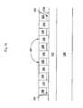
- FIG. 4is a graph showing change in read current for a memory cell of an embodiment of the present invention as voltage in reverse bias across the diode increases.
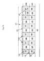
- FIG. 5is a probability plot showing memory cells transformed from the P state to the R state, and from the R state to the S state, then repeatably between the S state and the R state.
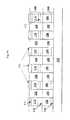
- FIG. 6is a circuit diagram showing a biasing scheme to bias the S cell in forward bias.
- FIG. 7is a circuit diagram showing one biasing scheme to bias the S cell in reverse bias.
- FIG. 8illustrates iterative read-verify-write cycles to move a cell into a data state.
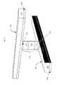
- FIGS. 9 a - 9 dare side cross-sectional views illustrating stages in formation of a memory level formed according to an embodiment of the present invention.
- FIGS. 10 a - 10 dare schematic side cross-sectional views illustrating alternative diode configurations according to an embodiment of the present invention.
- trimmable resistorshave been used as elements in integrated circuits.
- Leakage currentcan be greatly reduced by forming each memory cell as a two-terminal device including a diode.
- a diodehas a non-linear I-V characteristic, allowing very little current flow below a turn-on voltage, and substantially higher current flow above the turn-on voltage.
- a diodealso acts as one-way valves passing current more easily in one direction than the other.
- a memory element formed of doped semiconductor materialfor example the semiconductor diode of U.S. patent application Ser. No. 10/955,549, “Nonvolatile Memory Cell Without a Dielectric Antifuse Having High- and Low-Impedance States,” filed Sep. 29, 2004, hereinafter the '549 application and hereby incorporated by reference, can achieve three, four, or more stable resistivity states.
- semiconductor materialcan be converted from an initial low-resistivity state to a higher-resistivity state; then, upon application of an appropriate electrical pulse, can be returned to a lower-resistivity state.
- These embodimentscan be employed independently or combined to form a memory cell which can have two or more data states, and can be one-time-programmable or rewriteable.
- a diode between conductors in the memory cellallows its formation in a highly dense cross-point memory array.
- a polycrystalline, amorphous, or microcrystalline semiconductor memory elementis formed of the diode itself.
- transition from a higher resistivity, unprogrammed state to a lower resistivity, programmed statewill be called a set transition, affected by a set current, a set voltage, or a set pulse; while the reverse transition, from a lower resistivity, programmed state to a higher resistivity, unprogrammed state, will be called a reset transition, affected by a reset current, a reset voltage, or a reset pulse.
- the higher resistivity, unprogrammed statecorresponds to a “1” memory state
- the lower resistivity, programmed statecorresponds to a “0” memory state.
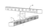
- FIG. 2illustrates a memory cell formed according to a preferred embodiment of the present invention.
- a bottom conductor 12is formed of a conductive material, for example tungsten, and extends in a first direction. Barrier and adhesion layers may be included in bottom conductor 12 .
- Polycrystalline semiconductor diode 2has a bottom heavily doped n-type region 4 ; an intrinsic region 6 , which is not intentionally doped; and a top heavily doped p-type region 8 , though the orientation of this diode may be reversed. Such a diode, regardless of its orientation, will be referred to as a p-i-n diode.
- Top conductor 16may be formed in the same manner and of the same materials as bottom conductor 12 , and extends in a second direction different from the first direction.
- Polycrystalline semiconductor diode 2is vertically disposed between bottom conductor 12 and top conductor 16 .
- Polycrystalline semiconductor diode 2is formed in a low-resistivity state.
- This memory cellcan be formed above a suitable substrate, for example above a monocrystalline silicon wafer.
- FIG. 3shows a portion of a memory level of such devices formed in a cross-point array, where diodes 2 are disposed between bottom conductors 12 and top conductors 16 .
- Multiple memory levelscan be stacked over a substrate to form a highly dense monolithic three dimensional memory array.
- the nonvolatile memory cellwhich consists essentially of the diode 2 and the electrically conductive electrodes 12 and 16 contacting the diode.
- the memory celldoes not include any active or passive device, such as a transistor, a capacitor, a resistor, a fuse, an antifuse, a charge storage material, a phase change material or a resistivity change material, except the diode 2 .
- the memory cellmay also contain an insulating material which surrounds the diode, as will be described below, and other optional layers.
- the memory cellcomprises a read/write memory cell, such as a rewritable memory cell.
- the diode 2acts as the read/write element of the memory cell, by switching from a first resistivity state to a second resistivity state different from the first resistivity state in response to an applied bias (i.e., pulse) as will be explained in more detail below.
- the diodecomprises a polycrystalline semiconductor diode, such as a polycrystalline silicon, germanium or silicon-germanium p-i-n pillar diode having a substantially cylindrical shape.
- at least one electrode of the memory cellincludes a metal silicide layer 124 , such as titanium silicide, titanium germanide or titanium silicide-germanide layer, having the C 49 phase, in physical contact with the diode 2 .
- the silicide layer 124preferably does not extend the entire length of the adjacent electrode 16 , 400 , but is physically located only on the substantially cylindrical pillar shaped diode 2 , 111 .
- the silicide layeracts as a crystallization template for the semiconductor diode 2 such that the diode is fabricated in the low resistivity, programmed state without an electrical programming step.
- the low resistivity of the diodeis believed to be a result of a large grain size of the polycrystalline semiconductor material that is crystallized in contact with the crystallization template.
- an intrinsic regionmay in fact include a low concentration of p-type or n-type dopants. Dopants may diffuse into the intrinsic region from adjacent regions, or may be present in the deposition chamber during deposition due to contamination from an earlier deposition. It will further be understood that deposited intrinsic semiconductor material (such as silicon) may include defects which cause it to behave as if slightly n-doped. Use of the term “intrinsic” to describe silicon, germanium, a silicon-germanium alloy, or some other semiconductor material is not meant to imply that this region contains no dopants whatsoever, nor that such a region is perfectly electrically neutral.
- the resistivity of doped polycrystalline or microcrystalline semiconductor materialcan be changed between stable states by applying appropriate electrical pulses. It has been found that in preferred embodiments, set transitions are advantageously performed with the diode under forward bias, while reset transitions are most readily achieved and controlled with the diode under reverse bias. In some instances, however, set transitions may be achieved with the diode under reverse bias, while reset transitions are achieved with the diode under forward bias.
- Switching under reverse biasshows a distinct behavior.
- a polysilicon p-i-n diodesuch as the one shown in FIG. 2 is subjected to a relatively large switching pulse under reverse bias.
- a smaller read pulsefor example 2 volts
- the read currentis measured.
- the subsequent read currentat two volts changes as shown in FIG. 4 . It will be seen that initially as the reverse voltage and current of the switching pulse are increased, the read current, when a read voltage is applied after each switching pulse, increases; i.e.
- the initial transition of the semiconductor material(silicon, in this case) is in the set direction toward lower resistivity.
- the switching pulsereaches a certain critical reverse bias voltage, at point K in FIG. 4 , about ⁇ 14.6 volts in this example, the read current abruptly begins to drop as reset is achieved and resistivity of the silicon increases.
- the switching voltage at which the set trend is reversed and the silicon of the diode begins to resetvaries, depending on, for example, the resistivity state of the silicon making up the diode when application of the reverse bias switching pulse is begun. It will be seen, then, that by selecting appropriate voltages, either set or reset of the semiconductor material making up the diode can be achieved with the diode under reverse bias.
- Distinct data states of the memory cell of the embodiments of the present inventioncorrespond to resistivity states of polycrystalline or microcrystalline semiconductor material making up the diode, which are distinguished by detecting current flow through the memory cell (between top conductor 16 and bottom conductor 12 ) when a read voltage is applied.
- the current flowing between any one distinct data state and any different distinct data stateis at least a factor of two, to allow the difference between the states to be readily detectable.
- the memory cellcan be used as a one-time programmable cell or a rewriteable memory cell, and may have two, three, four, or more distinct data states.
- the cellcan be converted from any of its data states to any other of its data states in any order, and under either forward or reverse bias.
- the memory cellbehaves as a rewriteable memory cell, which is repeatably switchable between two or between three data states.
- the memory cellis formed in a low resistivity, programmed state P.
- the formation of the memory cell in the high resistivity, unprogrammed state V and the application of the forward bias electrical pulse which switches the semiconductor material of diode 2 from the high resistivity state V to the low resistivity state Pis avoided.
- This simplifies the programming and handling of the memory cellbecause the device fabrication factory does not have to program the memory cells to the low resistivity, programmed P state before providing the memory device to the end users, since for most rewriteable embodiments, the initial V state does not serve as a data state of the memory cell.
- a first electrical pulsepreferably with diode 2 under reverse bias, is applied between top conductor 16 and bottom conductor 12 .
- the pulse magnitudeis above a predetermined critical voltage required to switch the resistivity state of the diode 2 .
- the voltageis between about ⁇ 8 and about ⁇ 14 volts, preferably between about ⁇ 9 and about ⁇ 13 volts, more preferably about ⁇ 10 or ⁇ 11 or ⁇ 13 or ⁇ 13.5 volts.
- the voltage requiredwill vary with the thickness of the intrinsic region.
- This electrical pulseswitches the semiconductor material of diode 2 from the low resistivity P state to a high resistivity R state.
- a second electrical pulsecan be applied between top conductor 16 and bottom conductor 12 , preferably under forward bias.
- the pulse magnitudeis above a predetermined critical voltage required to switch the resistivity state of the diode 2 .
- This pulseis, for example, between about 5.5 and about 9 volts, such as between about 6 to about 8 volts, preferably about 6.5 volts, with current between about 10 and about 200 microamps, preferably between about 50 and about 100 microamps.
- This electrical pulseswitches the semiconductor material of diode 2 from the high resistivity, unprogrammed R state to a low resistivity, programmed S state.
- the R and/or S statescorrespond to a data state of the memory cell.
- the R state and the S stateare sensed, or read, as data states.
- the memory cellcan repeatedly be switched between these two states. For example, a third electrical pulse, preferably with diode 2 under reverse bias, switches the semiconductor material of the diode from the low resistivity state S to the high resistivity state R. A fourth electrical pulse, preferably with diode 2 under forward bias, switches the semiconductor material of the diode from the high resistivity state R to the low resistivity state S, and so on.
- the difference between current flow under read voltage, for example of 2 volts, between top conductor 16 and bottom conductor 12 between any cell in one data state and any cell in an adjacent data states, in this case the R data state (between about 10 and about 500 nanoamps) and the S data state (between about 1.5 and about 4.5 microamps),is at least a factor of three.
- the differencemay be a factor of two, three, five, or more.
- a rewriteable memory cellcan be switched between three or more data states, in any order. Either set or reset transitions can be performed with the diode under either forward or reverse bias.
- the data statecorresponds to the resistivity state of polycrystalline or microcrystalline semiconductor material making up a diode.
- the data statesdoes not correspond to the resistivity state of a resistivity-switching metal oxide or nitride, as in Herner et al., U.S. patent application Ser. No. 11/395,995, “Nonvolatile Memory Cell Comprising a Diode and a Resistance-Switching Material,” filed Mar. 31, 2006, owned by the assignee of the present invention and hereby incorporated by reference.
- any step in which cells are subjected to large voltages in reverse biashas reduced leakage current as compared to a forward bias step.
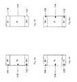
- Bitline B 0is set at 10 volts and wordline W 0 is set at ground.
- wordline W 1is set less than but relatively close to the voltage of bitline B 0 ; for example wordline W 1 may be set to 9.3 volts, so that 0.7 volts is applied across the F cells (only one F cell is shown, but there may be hundreds, thousands or more.)
- bitline B 1is set higher than but relatively close to the voltage of wordline W 0 ; for example bitline B 1 may be set to 0.7 volts, so that 0.7 volts is applied across cell H (again, there may be thousands of H cells.)
- the unselected cells Uwhich share neither wordline W 0 or bitline B 0 with selected cell S, are subjected to ⁇ 8.6 volts. As there may be millions of unselected cells U
- FIG. 7shows an advantageous biasing scheme to apply a large reverse bias across a memory cell, for example as a reset pulse.
- Bitline B 0is set at ⁇ 5 volts and wordline W 0 at 5 volts, so that ⁇ 10 volts is applied across selected cell S; the diode is in reverse bias.
- Setting wordline W 1 and bitline B 1 at groundsubjects both half-selected cells F and H to ⁇ 5 volts, at a reverse bias low enough not to cause unintentional set or reset of these cells.
- Set or reset in reverse biasgenerally seems to take place at or near the voltage at which the diode goes into reverse breakdown, which is generally higher than ⁇ 5 volts.
- bitline B 0can be set at 0 volts, wordline W 0 at ⁇ 10 volts, and bitline B 1 and wordline W 1 at ⁇ 5 volts.
- the voltage across selected cell S, half-selected cells H and F, and unselected cells Uwill be the same as in the scheme of FIG. 7 .
- bitline B 0is set at ground, wordline W 0 at 10 volts, and bitline B 1 and wordline W 1 each at 5 volts.
- the difference between current flow during read in adjacent data statesis preferably at least a factor of two; in many embodiments, it may be preferred to establish current ranges for each data state which are separated by a factor of three, five, ten, or more.
- data state Vmay be omitted by fabricating the diode in the low resistivity, programmed state.
- the data state Rcan be defined as read current between about 10 and about 500 nanoamps, data state S as read current between about 1.5 and about 4.5 microamps, and data state P as read current above about 10 microamps. Those skilled in the art will appreciate that these are examples only. Actual read currents will vary with characteristics of the cell, construction of the array, read voltage selected, and many other factors.
- a one-time programmable memory cellis in data state P.
- An electrical pulse in reverse biasis applied to the memory cell to switch the cell into data state S.
- the read currentis not in the desired range; i.e. the resistivity state of the semiconductor material of the diode is higher or lower than intended.
- the read current of the memory cellis at the point on the graph shown at Q, in between the S state and P state current ranges.
- the memory cellmay be read to determine if the desired data state was reached. If the desired data state was not reached, an additional pulse is applied. For example, when the current Q is sensed, an additional reset pulse is applied to increase the resistivity of the semiconductor material, decreasing the read current into the range corresponding to the S data state. As described earlier, this set pulse may be applied in either forward or reverse bias. The additional pulse or pulses may have a higher amplitude (voltage or current) or longer or shorter pulse width than the original pulse. After the additional set pulse, the cell is read again, then set or reset pulses applied as appropriate until the read current is in the desired range.
- a two-terminal devicesuch as the memory cell including a diode described
- Applying a large reverse bias across the diodemay damage the diode; thus when performing a set or reset with the diode under reverse bias, it is advantageous to minimize the reverse bias voltage.
- Fabrication of a single memory levelwill be described in detail. Additional memory levels can be stacked, each monolithically formed above the one below it. In this embodiment, a polycrystalline semiconductor diode will serve as the switchable memory element.
- This substrate 100can be any semiconducting substrate as known in the art, such as monocrystalline silicon, IV-IV compounds such as silicon-germanium or silicon-germanium-carbon, III-V compounds, II-VII compounds, epitaxial layers over such substrates, or any other semiconducting or non-semiconducting material.
- the substratemay include integrated circuits fabricated therein.
- the insulating layer 102is formed over substrate 100 .
- the insulating layer 102can be silicon oxide, silicon nitride, high-dielectric film, Si—C—O—H film, or any other suitable insulating material.
- the first conductors 200are formed over the substrate and insulator.
- An adhesion layer 104may be included between the insulating layer 102 and the conducting layer 106 to help conducting layer 106 adhere to insulating layer 102 . If the overlying conducting layer is tungsten, titanium nitride is preferred as adhesion layer 104 .
- Conducting layer 106can comprise any conducting material known in the art, such as tungsten, or other materials, including tantalum, titanium, copper, cobalt, or alloys thereof.
- the layerswill be patterned and etched using any suitable masking and etching process to form substantially parallel, substantially coplanar conductors 200 , shown in FIG. 9 a in cross-section.
- photoresistis deposited, patterned by photolithography and the layers etched, and then the photoresist removed using standard process techniques.
- Conductors 200could be formed by a Damascene method instead.
- Dielectric material 108is deposited over and between conductor rails 200 .
- Dielectric material 108can be any known electrically insulating material, such as silicon oxide, silicon nitride, or silicon oxynitride. In a preferred embodiment, silicon dioxide is used as dielectric material 108 .
- FIG. 9 aThis removal of dielectric overfill to form planar surface 109 can be performed by any process known in the art, such as chemical mechanical planarization (CMP) or etchback.
- CMPchemical mechanical planarization
- An etchback technique that may advantageously be usedis described in Raghuram et al., U.S. application Ser. No. 10/883,417, “Nonselective Unpatterned Etchback to Expose Buried Patterned Features,” filed Jun. 30, 2004 and hereby incorporated by reference.
- a plurality of substantially parallel first conductorshave been formed at a first height above substrate 100 .
- a barrier layer 110is deposited as the first layer after planarization of the conductor rails.
- Any suitable materialcan be used in the barrier layer, including tungsten nitride, tantalum nitride, titanium nitride, or combinations of these materials.
- titanium nitrideis used as the barrier layer.
- the barrier layeris titanium nitride, it can be deposited in the same manner as the adhesion layer described earlier.
- the semiconductor materialcan be silicon, germanium, a silicon-germanium alloy, or other suitable semiconductors, or semiconductor alloys.
- the semiconductor materialis deposited in a relatively highly resistive amorphous or polycrystalline (which includes microcrystalline) state.
- the pillarcomprises a semiconductor junction diode.
- junction diodeis used herein to refer to a semiconductor device with the property of non-ohmic conduction, having two terminal electrodes, and made of semiconducting material which is p-type at one electrode and n-type at the other. Examples include p-n diodes and n-p diodes, which have p-type semiconductor material and n-type semiconductor material in contact, such as Zener diodes, and p-i-n diodes, in which intrinsic (undoped) semiconductor material is interposed between p-type semiconductor material and n-type semiconductor material.
- Bottom heavily doped region 112can be formed by any deposition and doping method known in the art.
- the siliconcan be deposited and then doped, but is preferably doped in situ by flowing a donor gas providing n-type dopant atoms, for example phosphorus, during deposition of the silicon.
- Heavily doped region 112is preferably between about 10 and about 80 nm thick.
- Intrinsic layer 114can be formed by any method known in the art.
- Layer 114can be silicon, germanium, or any alloy of silicon or germanium and has a thickness between about 110 and about 330 nm, preferably about 200 nm.
- Pillars 300should have about the same pitch and about the same width as conductors 200 below, such that each pillar 300 is formed on top of a conductor 200 . Some misalignment can be tolerated.
- the pillars 300can be formed using any suitable masking and etching process.
- photoresistcan be deposited, patterned using standard photolithography techniques, and etched, then the photoresist removed.
- a hard mask of some other materialfor example silicon dioxide, can be formed on top of the semiconductor layer stack, with bottom antireflective coating (BARC) on top, then patterned and etched.
- BARCbottom antireflective coating
- DARCdielectric antireflective coating
- the pitch and width of the pillars 300can be varied as desired.
- the pitch of the pillars(the distance from the center of one pillar to the center of the next pillar) is about 300 nm, while the width of a pillar varies between about 100 and about 150 nm.
- the pitch of the pillarsis about 260 nm, while the width of a pillar varies between about 90 and 130 nm.
- the pillarspreferably have a substantially cylindrical shape with a circular or roughly circular cross section having a diameter of 250 nm or less.
- a “substantially cylindrical” elementis one with a cross section which is roughly circular; more specifically, a cross section in which no portion of the perimeter is a straight edge for a length longer than fifty percent of the longest dimension measured through the centroid of the cross-sectional area.
- a straight edgewill not be “straight” to a molecular level, and may have minute irregularities; what is relevant is the degree of rounding, as described in U.S. Pat. No. 6,952,030, incorporated herein by reference.
- Dielectric material 108is deposited over and between the semiconductor pillars 300 , filling the gaps between them.
- Dielectric material 108can be any known electrically insulating material, such as silicon oxide, silicon nitride, or silicon oxynitride. In a preferred embodiment, silicon dioxide is used as the insulating material.
- the dielectric material on top of the pillars 300is removed, exposing the tops of pillars 300 separated by dielectric material 108 , and leaving a substantially planar surface.
- This removal of dielectric overfillcan be performed by any process known in the art, such as CMP or etchback.
- the insulating layer 108is planarized such that it surrounds the semiconductor region of the pillar 300 .
- ion implantationis performed, forming heavily doped p-type top region 116 .
- the p-type dopantis preferably boron or BF 2 .
- This implant stepcompletes formation of diodes 111 .
- region 116may be deposited as a layer on layer 114 before the pillar patterning step rather than being implanted into layer 114 .
- the resulting structureis shown in FIG. 9 b and schematically in FIG. 10 a.
- FIGS. 10 b to 10 dillustrate other permutations of diode structures.
- bottom region 112is N+ (heavily doped n-type silicon), and top region 116 is P+.
- top region 116is P+.
- bottom region 112is P+ and top region 116 is N+.
- middle region 114is N ⁇ , while in FIGS. 5 b and 5 d , middle region 114 is P ⁇ .
- the middle regioncan intentionally be lightly doped, or it can be intrinsic, or not intentionally doped.
- An undoped regionwill never be perfectly electrically neutral, and will always have defects or contaminants that cause it to behave as if slightly n-doped or p-doped.
- Such a diodecan be considered a p-i-n diode.
- a P+/N ⁇ /N+, P+/P ⁇ /N+, N+/N ⁇ /P+ or N+/P ⁇ /P+ diodecan be formed.
- an optional insulating oxide, nitride, or oxynitride layer 118may be formed on heavily doped regions 116 .
- Layer 118will be reduced during formation of a titanium silicide layer 124 (but generally not other metal silicide layers), as will be described below.
- layer 118may be omitted.
- the optional silicon dioxide layer 118is grown by oxidizing silicon at the tops of heavily doped regions 116 at about 600 to about 850° C. for about 20 seconds to about two minutes, forming between about 1 and about 5 nm of silicon dioxide.
- oxide layer 118is formed by exposing the wafer to about 800 degrees for about one minute in an oxygen-containing ambient. Layer 118 could be deposited instead.
- a layer 120 of a silicide-forming metalis deposited.
- Preferred silicide-forming metals to be used for this purposeinclude titanium or cobalt. This example will describe the use of titanium for layer 120 , but it will be understood that other materials can be used.
- Titanium layer 120is deposited to any suitable thickness, for example between about 1 and about 20 nm, preferably between about 10 and about 15 nm, most preferably about 10 nm.
- titanium nitride layer 122is deposited, preferably about 30 nm thick. Layers 120 and 122 can be deposited by any conventional method, for example by sputtering.
- An annealis performed between about 600 and about 800° C. from about 10 seconds to about two minutes, preferably between about 650 degrees and about 750 degrees, most preferably at about 670 degrees for about 20 seconds, for example in nitrogen.
- the annealserves to reduce oxide layer 118 and to react titanium layer 120 with heavily doped regions 116 where it overlies them to form titanium silicide.
- Oxide layer 118is substantially entirely reduced between titanium layer 120 and the silicon of heavily doped region 116 . If oxide layer 118 was deposited rather than grown, the rest of oxide layer 118 (between the tops of semiconductor pillars 300 , overlying dielectric fill 108 ) would remain.
- titanium nitride layer 122 and unreacted titaniumare stripped in a selective wet etch, leaving behind titanium silicide layers 124 , each formed in a disk-shaped region on the top of one of the junction diodes, shown in FIG. 9 d.
- the titanium silicide feature 124 that is formed during the annealcomprises C 49 phase titanium silicide.
- the C 49 phasecan be obtained if the annealing temperature is maintained below 700 degrees C. for large or small sized silicon features or if the annealing temperature is maintained above 700 degrees C., but the silicon feature size is 0.25 microns or less.
- the diameter of the diode 2is preferably 0.25 microns or less to form the C 49 phase of titanium silicide for annealing temperature above 700 degrees C. This phase is desired due to its lattice match with amorphous silicon during the crystallization process.
- the titanium silicideIn contrast larger features (greater than a dimensional size of 0.25 microns) will allow the titanium silicide to end as the C 54 phase of titanium silicide during subsequent annealing above 700 degrees C. Even though the C 54 phase provides low resistivity (which is highly desired by integrated circuit manufactures), it does not provide as good a lattice match during the crystallization process of the amorphous or polycrystalline silicon. Thus, the C 49 phase titanium silicide allows for the greatest enhancement to grain growth and thus a lower diode resistivity by acting as a crystallization template for the semiconductor material of the diode.
- titanium silicide layer 124could instead be some other silicide, such as cobalt silicide.
- each pillarcomprising a silicide layer 124 .
- the junction diodeis amorphous silicon as deposited, and is crystallized to form large grain, low resistivity polysilicon in contact with a silicide layer 124 .
- the crystallizationcan occur during the formation of the silicide 124 and/or during a separate crystallization anneal after the memory cell is completed.
- the separate crystallization annealmay be conducted at a temperature above about 600° C., such as 650 to 850° C. for 1 or more minutes, such as 2 minutes to 24 hours, depending on the desired degree of crystallization. A lower temperature may be used for germanium and silicon germanium diode materials.
- the silicide layer 124is advantageous for reducing the impedance of the junction diode, but may not be desired in the finished device. In an alternative embodiment, following formation of the silicide layer on the junction diode, the silicide layer can be removed.
- FIG. 11illustrates a completed memory cell.
- Top conductors 400i.e., the upper electrode 16 shown in FIG. 2
- Conductive layer 422 and adhesion layer 420are then patterned and etched using any suitable masking and etching technique to form substantially parallel, substantially coplanar conductors 400 , shown in FIG. 11 extending perpendicular to conductors 200 .
- photoresistis deposited, patterned by photolithography and the layers etched, and then the photoresist removed using standard process techniques.
- the dielectric materialcan be any known electrically insulating material, such as silicon oxide, silicon nitride, or silicon oxynitride. In a preferred embodiment, silicon oxide is used as this dielectric material.
- Formation of a first memory levelhas been described. Additional memory levels can be formed above this first memory level to form a monolithic three dimensional memory array.
- conductorscan be shared between memory levels; i.e. top conductor 400 would serve as the bottom conductor of the next memory level.
- an interlevel dielectric(not shown) is formed above the first memory level of FIG. 11 , its surface planarized, and construction of a second memory level begins on this planarized interlevel dielectric, with no shared conductors.
- a monolithic three dimensional memory arrayis one in which multiple memory levels are formed above a single substrate, such as a wafer, with no intervening substrates.
- the layers forming one memory levelare deposited or grown directly over the layers of an existing level or levels.
- stacked memorieshave been constructed by forming memory levels on separate substrates and adhering the memory levels atop each other, as in Leedy, U.S. Pat. No. 5,915,167, “Three dimensional structure memory.”
- the substratesmay be thinned or removed from the memory levels before bonding, but as the memory levels are initially formed over separate substrates, such memories are not true monolithic three dimensional memory arrays.
- Monolithic three dimensional memory arraysare described in Johnson et al., U.S. Pat. No. 6,034,882, “Vertically stacked field programmable nonvolatile memory and method of fabrication”; Johnson, U.S. Pat. No. 6,525,953, “Vertically stacked field programmable nonvolatile memory and method of fabrication”; Knall et al., U.S. Pat. No. 6,420,215, “Three Dimensional Memory Array and Method of Fabrication”; Herner, U.S. application Ser. No. 10/095,962, “Silicide-Silicon Oxide-Semiconductor Antifuse Device and Method of Making,” filed Mar.
- the present inventionhas been described herein in the context of a monolithic three dimensional memory array formed above a substrate.
- Such an arraycomprises at least a first memory level formed at a first height above the substrate and a second memory level formed at a second height different from the first height.
- Three, four, eight, or more memory levelscan be formed above the substrate in such a multilevel array.
- Each memory levelis monolithically formed on the memory level below it.
- the memory cell of the present inventionhas been described as formed in a monolithic three dimensional memory array having stacked memory levels, but such cells could clearly be formed in a two-dimensional array, as well.
- the example givenshowed the silicide layer formed above the junction diode, but those skilled in the art will appreciate that the silicide layer can be formed elsewhere: beside the junction diode or below it, for example. Many configurations can be imagined.
- a silicide layeris formed only on the semiconductor pillar.
- a silicide layerextends the entire length of one or both electrodes.
Landscapes
- Engineering & Computer Science (AREA)
- Computer Hardware Design (AREA)
- Semiconductor Memories (AREA)
Abstract
Description
- This application is a continuation-in-part of U.S. application Ser. No. 11/496,986 filed on Jul. 31, 2006, which is a continuation-in part of U.S. application Ser. No. 11/237,167, filed on Sep. 28, 2005. This application is also a continuation-in-part of U.S. application Ser. No. 11/613,151 filed on Dec. 19, 2006, which is a divisional of U.S. application Ser. No. 10/954,510 filed on Sep. 29, 2004, now U.S. Pat. No. 7,176,064, which is a continuation-in-part of U.S. application Ser. No. 10/728,230, filed on Dec. 3, 2002, now U.S. Pat. No. 6,946,719. This application is also a continuation-in-part of U.S. application Ser. No. 10/955,459 filed on Sep. 29, 2004 which is a continuation-in-part of U.S. application Ser. No. 10/855,784 filed on May 26, 2004, which is a continuation-in-part of U.S. application Ser. No. 10/326,470 filed on Dec. 19, 2002, now abandoned. All of the above applications are hereby incorporated by reference in their entirety. This application is related to Kumar et al., U. S. application Ser. No. __ /______, titled “METHOD OF MAKING A DIODE READ/WRITE MEMORY CELL IN A PROGRAMMED STATE,” (Attorney Docket No. 035905/0152), filed on the same day herewith, and hereby incorporated by reference in its entirety.
- The invention relates to a nonvolatile memory array.
- Nonvolatile memory arrays maintain their data even when power to the device is turned off. In one-time-programmable arrays, each memory cell is formed in an initial unprogrammed state, and can be converted to a programmed state. This change is permanent, and such cells are not erasable. In other types of memories, the memory cells are erasable, and can be rewritten many times.
- Cells may also vary in the number of data states each cell can achieve. A data state may be stored by altering some characteristic of the cell which can be detected, such as current flowing through the cell under a given applied voltage or the threshold voltage of a transistor within the cell. A data state is a distinct value of the cell, such as a data ‘0’ or a data ‘1’.
- Some solutions for achieving erasable or multi-state cells are complex. Floating gate and SONOS memory cells, for example, operate by storing charge, where the presence, absence or amount of stored charge changes a transistor threshold voltage. These memory cells are three-terminal devices which are relatively difficult to fabricate and operate at the very small dimensions required for competitiveness in modem integrated circuits.
- Other memory cells operate by changing the resistivity of relatively exotic materials, like chalcogenides. Chalcogenides are difficult to work with and can present challenges in most semiconductor production facilities.
- A substantial advantage would be provided by a nonvolatile memory array having erasable or multi-state memory cells formed using conventional semiconductor materials in structures that are readily scaled to small size.
- One embodiment of the invention provides a nonvolatile memory device comprising at least one memory cell which consists essentially of a diode and electrically conductive electrodes contacting the diode, wherein the diode is fabricated in a low resistivity, programmed state.
- Another embodiment of the invention provides a nonvolatile memory device comprising a plurality of memory cells. Each memory cell comprises a first electrode, a polycrystalline silicon, germanium or silicon-germanium diode electrically contacting the first electrode, and a second electrode electrically contacting the diode. The second electrode comprises a titanium silicide, titanium germanide or titanium silicide-germanide layer having a C49 phase which physically contacts the diode.
- Another embodiment of the invention provides a nonvolatile memory device comprising a read/write memory cell comprising a first electrode, a diode which is fabricated in a low resistivity programmed state, and a second electrode, and a means for applying a reverse bias above the diode's critical voltage value to the diode to switch the diode from the low resistivity programmed state to a high resistivity, unprogrammed state, and for applying a forward bias to the diode to switch the diode to the low resistivity, programmed state.
- Each of the aspects and embodiments of the invention described herein can be used alone or in combination with one another. The preferred aspects and embodiments will now be described with reference to the attached drawings.
FIG. 1 is a circuit diagram illustrating the need for electrical isolation between memory cells in a memory array.FIGS. 2 and 11 are perspective views of memory cells formed according to a preferred embodiment of the present invention.FIG. 3 is a perspective view of a portion of a memory level comprising the memory cells ofFIG. 2 .FIG. 4 is a graph showing change in read current for a memory cell of an embodiment of the present invention as voltage in reverse bias across the diode increases.FIG. 5 is a probability plot showing memory cells transformed from the P state to the R state, and from the R state to the S state, then repeatably between the S state and the R state.FIG. 6 is a circuit diagram showing a biasing scheme to bias the S cell in forward bias.FIG. 7 is a circuit diagram showing one biasing scheme to bias the S cell in reverse bias.FIG. 8 illustrates iterative read-verify-write cycles to move a cell into a data state.FIGS. 9 a-9dare side cross-sectional views illustrating stages in formation of a memory level formed according to an embodiment of the present invention.FIGS. 10 a-10dare schematic side cross-sectional views illustrating alternative diode configurations according to an embodiment of the present invention.- It has been known that by applying electrical pulses, the resistance of a resistor formed of doped polycrystalline silicon, or polysilicon, can be trimmed, adjusting it between stable resistance states. Such trimmable resistors have been used as elements in integrated circuits.
- It is not conventional to use a trimmable polysilicon resistor to store a data state in a nonvolatile memory cell, however. Making a memory array of polysilicon resistors presents difficulties. If resistors are used as memory cells in a large cross-point array, when voltage is applied to a selected cell, there will be undesired leakage through half-selected and unselected cells throughout the array. For example, turning to
FIG. 1 , suppose a voltage is applied between bitline B and wordline A to set, reset, or sense selected cell S. Current is intended to flow through selected cell S. Some leakage current, however, may flow on alternate paths, for example between bitline B and wordline A through unselected cells U1, U2, and U3. Many such alternate paths may exist. - Leakage current can be greatly reduced by forming each memory cell as a two-terminal device including a diode. A diode has a non-linear I-V characteristic, allowing very little current flow below a turn-on voltage, and substantially higher current flow above the turn-on voltage. In general a diode also acts as one-way valves passing current more easily in one direction than the other. Thus, so long as biasing schemes are selected that assure that only the selected cell is subjected to a forward current above the turn-on voltage, leakage current along unintended paths (such as the U1-U2-U3 sneak path of
FIG. 1 ) can be greatly reduced. - In embodiments of the present invention, by applying appropriate electrical pulses, a memory element formed of doped semiconductor material, for example the semiconductor diode of U.S. patent application Ser. No. 10/955,549, “Nonvolatile Memory Cell Without a Dielectric Antifuse Having High- and Low-Impedance States,” filed Sep. 29, 2004, hereinafter the '549 application and hereby incorporated by reference, can achieve three, four, or more stable resistivity states. In other embodiments of the present invention, semiconductor material can be converted from an initial low-resistivity state to a higher-resistivity state; then, upon application of an appropriate electrical pulse, can be returned to a lower-resistivity state. These embodiments can be employed independently or combined to form a memory cell which can have two or more data states, and can be one-time-programmable or rewriteable.
- Herner et al., U.S. patent application Ser. No. 11/148,530, “Nonvolatile Memory Cell Operating by Increasing Order in Polycrystalline Semiconductor Material,” filed Jun. 8, 2006; and Herner, U.S. patent application Ser. No. 10/954,510, “Memory Cell Comprising a Semiconductor Junction Diode Crystallized Adjacent to a Silicide,” filed Sep. 29, 2004, both owned by the assignee of the present invention and both hereby incorporated by reference, describe that crystallization of polysilicon adjacent to an appropriate silicide affects the properties of the polysilicon. Certain metal silicides, such as cobalt silicide and titanium silicide, have a lattice structure very close to that of silicon. When amorphous or microcrystalline silicon is crystallized in contact with one of these silicides, the crystal lattice of the silicide provides a template to the silicon during crystallization. The resulting polysilicon will be highly ordered, and relatively low in defects. This high-quality polysilicon, when doped with a conductivity-enhancing dopant, is relatively highly conductive as formed.
- As noted, including a diode between conductors in the memory cell allows its formation in a highly dense cross-point memory array. In preferred embodiments of the present invention, then, a polycrystalline, amorphous, or microcrystalline semiconductor memory element is formed of the diode itself.
- In this discussion, transition from a higher resistivity, unprogrammed state to a lower resistivity, programmed state will be called a set transition, affected by a set current, a set voltage, or a set pulse; while the reverse transition, from a lower resistivity, programmed state to a higher resistivity, unprogrammed state, will be called a reset transition, affected by a reset current, a reset voltage, or a reset pulse. The higher resistivity, unprogrammed state corresponds to a “1” memory state, while the lower resistivity, programmed state corresponds to a “0” memory state.
FIG. 2 illustrates a memory cell formed according to a preferred embodiment of the present invention. Abottom conductor 12 is formed of a conductive material, for example tungsten, and extends in a first direction. Barrier and adhesion layers may be included inbottom conductor 12.Polycrystalline semiconductor diode 2 has a bottom heavily doped n-type region 4; anintrinsic region 6, which is not intentionally doped; and a top heavily doped p-type region 8, though the orientation of this diode may be reversed. Such a diode, regardless of its orientation, will be referred to as a p-i-n diode.Top conductor 16 may be formed in the same manner and of the same materials asbottom conductor 12, and extends in a second direction different from the first direction.Polycrystalline semiconductor diode 2 is vertically disposed betweenbottom conductor 12 andtop conductor 16.Polycrystalline semiconductor diode 2 is formed in a low-resistivity state. This memory cell can be formed above a suitable substrate, for example above a monocrystalline silicon wafer.FIG. 3 shows a portion of a memory level of such devices formed in a cross-point array, wherediodes 2 are disposed betweenbottom conductors 12 andtop conductors 16. Multiple memory levels can be stacked over a substrate to form a highly dense monolithic three dimensional memory array.- Preferably, the nonvolatile memory cell which consists essentially of the
diode 2 and the electricallyconductive electrodes diode 2. The memory cell may also contain an insulating material which surrounds the diode, as will be described below, and other optional layers. The memory cell comprises a read/write memory cell, such as a rewritable memory cell. Thediode 2 acts as the read/write element of the memory cell, by switching from a first resistivity state to a second resistivity state different from the first resistivity state in response to an applied bias (i.e., pulse) as will be explained in more detail below. - As shown in
FIG. 2 , the diode comprises a polycrystalline semiconductor diode, such as a polycrystalline silicon, germanium or silicon-germanium p-i-n pillar diode having a substantially cylindrical shape. As will be explained in more detail with respect toFIG. 11 , at least one electrode of the memory cell includes ametal silicide layer 124, such as titanium silicide, titanium germanide or titanium silicide-germanide layer, having the C49 phase, in physical contact with thediode 2. As shown inFIG. 11 , thesilicide layer 124 preferably does not extend the entire length of theadjacent electrode diode semiconductor diode 2 such that the diode is fabricated in the low resistivity, programmed state without an electrical programming step. Without wishing to be bound by a particular theory, the low resistivity of the diode is believed to be a result of a large grain size of the polycrystalline semiconductor material that is crystallized in contact with the crystallization template. - In this discussion, a region of semiconductor material which is not intentionally doped is described as an intrinsic region. It will be understood by those skilled in the art, however, that an intrinsic region may in fact include a low concentration of p-type or n-type dopants. Dopants may diffuse into the intrinsic region from adjacent regions, or may be present in the deposition chamber during deposition due to contamination from an earlier deposition. It will further be understood that deposited intrinsic semiconductor material (such as silicon) may include defects which cause it to behave as if slightly n-doped. Use of the term “intrinsic” to describe silicon, germanium, a silicon-germanium alloy, or some other semiconductor material is not meant to imply that this region contains no dopants whatsoever, nor that such a region is perfectly electrically neutral.
- The resistivity of doped polycrystalline or microcrystalline semiconductor material, for example silicon, can be changed between stable states by applying appropriate electrical pulses. It has been found that in preferred embodiments, set transitions are advantageously performed with the diode under forward bias, while reset transitions are most readily achieved and controlled with the diode under reverse bias. In some instances, however, set transitions may be achieved with the diode under reverse bias, while reset transitions are achieved with the diode under forward bias.
- Semiconductor switching behavior is complex. For a diode, both set and reset transitions have been achieved with the diode under forward bias. Generally a reset pulse applied with the diode under forward bias which is sufficient to switch the polycrystalline semiconductor material making up a diode from a given resistivity state to a higher resistivity state will be lower voltage amplitude than a corresponding set pulse (which will switch the same polysilicon semiconductor material from the same resistivity state to a lower resistivity state) and will have a longer pulse width.
- Switching under reverse bias shows a distinct behavior. Suppose a polysilicon p-i-n diode such as the one shown in
FIG. 2 is subjected to a relatively large switching pulse under reverse bias. After application of the switching pulse, a smaller read pulse, for example 2 volts, is applied, and the current flowing through the diode at the read voltage, called the read current, is measured. As the voltage of the switching pulse under reverse bias is increased in subsequent pulses, the subsequent read current at two volts changes as shown inFIG. 4 . It will be seen that initially as the reverse voltage and current of the switching pulse are increased, the read current, when a read voltage is applied after each switching pulse, increases; i.e. the initial transition of the semiconductor material (silicon, in this case) is in the set direction toward lower resistivity. Once the switching pulse reaches a certain critical reverse bias voltage, at point K inFIG. 4 , about −14.6 volts in this example, the read current abruptly begins to drop as reset is achieved and resistivity of the silicon increases. The switching voltage at which the set trend is reversed and the silicon of the diode begins to reset varies, depending on, for example, the resistivity state of the silicon making up the diode when application of the reverse bias switching pulse is begun. It will be seen, then, that by selecting appropriate voltages, either set or reset of the semiconductor material making up the diode can be achieved with the diode under reverse bias. - Distinct data states of the memory cell of the embodiments of the present invention correspond to resistivity states of polycrystalline or microcrystalline semiconductor material making up the diode, which are distinguished by detecting current flow through the memory cell (between
top conductor 16 and bottom conductor12) when a read voltage is applied. Preferably the current flowing between any one distinct data state and any different distinct data state is at least a factor of two, to allow the difference between the states to be readily detectable. - The memory cell can be used as a one-time programmable cell or a rewriteable memory cell, and may have two, three, four, or more distinct data states. The cell can be converted from any of its data states to any other of its data states in any order, and under either forward or reverse bias.
- Several examples of preferred embodiments will be provided. It will be understood, however, that these examples are not intended to be limiting. It will be apparent to those skilled in the art that other methods of programming a two-terminal device comprising a diode and polycrystalline or microcrystalline semiconductor material will fall within the scope of the invention.
- In one set of embodiments, the memory cell behaves as a rewriteable memory cell, which is repeatably switchable between two or between three data states.
- Turning to
FIG. 5 , in a first preferred embodiment, the memory cell is formed in a low resistivity, programmed state P. Thus, the formation of the memory cell in the high resistivity, unprogrammed state V and the application of the forward bias electrical pulse which switches the semiconductor material ofdiode 2 from the high resistivity state V to the low resistivity state P is avoided. This simplifies the programming and handling of the memory cell because the device fabrication factory does not have to program the memory cells to the low resistivity, programmed P state before providing the memory device to the end users, since for most rewriteable embodiments, the initial V state does not serve as a data state of the memory cell. - A first electrical pulse, preferably with
diode 2 under reverse bias, is applied betweentop conductor 16 andbottom conductor 12. The pulse magnitude is above a predetermined critical voltage required to switch the resistivity state of thediode 2. For example, the voltage is between about −8 and about −14 volts, preferably between about −9 and about −13 volts, more preferably about −10 or −11 or −13 or −13.5 volts. The voltage required will vary with the thickness of the intrinsic region. This electrical pulse switches the semiconductor material ofdiode 2 from the low resistivity P state to a high resistivity R state. - A second electrical pulse can be applied between
top conductor 16 andbottom conductor 12, preferably under forward bias. The pulse magnitude is above a predetermined critical voltage required to switch the resistivity state of thediode 2. This pulse is, for example, between about 5.5 and about 9 volts, such as between about 6 to about 8 volts, preferably about 6.5 volts, with current between about 10 and about 200 microamps, preferably between about 50 and about 100 microamps. This electrical pulse switches the semiconductor material ofdiode 2 from the high resistivity, unprogrammed R state to a low resistivity, programmed S state. In preferred embodiments, the R and/or S states correspond to a data state of the memory cell. - In this rewriteable, two-state embodiment, the R state and the S state are sensed, or read, as data states. The memory cell can repeatedly be switched between these two states. For example, a third electrical pulse, preferably with
diode 2 under reverse bias, switches the semiconductor material of the diode from the low resistivity state S to the high resistivity state R. A fourth electrical pulse, preferably withdiode 2 under forward bias, switches the semiconductor material of the diode from the high resistivity state R to the low resistivity state S, and so on. - As will be seen from
FIG. 5 , in the example provided, the difference between current flow under read voltage, for example of 2 volts, betweentop conductor 16 andbottom conductor 12 between any cell in one data state and any cell in an adjacent data states, in this case the R data state (between about 10 and about 500 nanoamps) and the S data state (between about 1.5 and about 4.5 microamps), is at least a factor of three. Depending on the ranges selected for each data state, the difference may be a factor of two, three, five, or more. - In alternative embodiments, a rewriteable memory cell can be switched between three or more data states, in any order. Either set or reset transitions can be performed with the diode under either forward or reverse bias.
- In the embodiments described, note that the data state corresponds to the resistivity state of polycrystalline or microcrystalline semiconductor material making up a diode. The data states does not correspond to the resistivity state of a resistivity-switching metal oxide or nitride, as in Herner et al., U.S. patent application Ser. No. 11/395,995, “Nonvolatile Memory Cell Comprising a Diode and a Resistance-Switching Material,” filed Mar. 31, 2006, owned by the assignee of the present invention and hereby incorporated by reference.
- In an array of memory cells formed and programmed according to the embodiments described so far, any step in which cells are subjected to large voltages in reverse bias has reduced leakage current as compared to a forward bias step.
- Turning to
FIG. 6 , suppose 10 volts is to be applied in forward bias across the selected cell S. (The actual voltage to be used will depend on many factors, including the construction of the cell, dopant levels, height of the intrinsic region, etc.; 10 volts is merely an example.) Bitline B0 is set at 10 volts and wordline W0 is set at ground. To assure that half-selected cells F (which share bitline B0 with selected cell S) remain below the turn-on voltage of the diode, wordline W1 is set less than but relatively close to the voltage of bitline B0; for example wordline W1 may be set to 9.3 volts, so that 0.7 volts is applied across the F cells (only one F cell is shown, but there may be hundreds, thousands or more.) Similarly, to assure that half-selected cells H (which share wordline W0 with selected cell S) remain below the turn-on voltage of the diode, bitline B1 is set higher than but relatively close to the voltage of wordline W0; for example bitline B1 may be set to 0.7 volts, so that 0.7 volts is applied across cell H (again, there may be thousands of H cells.) The unselected cells U, which share neither wordline W0 or bitline B0 with selected cell S, are subjected to −8.6 volts. As there may be millions of unselected cells U, this results in significant leakage current within the array. FIG. 7 shows an advantageous biasing scheme to apply a large reverse bias across a memory cell, for example as a reset pulse. Bitline B0 is set at −5 volts and wordline W0 at 5 volts, so that −10 volts is applied across selected cell S; the diode is in reverse bias. Setting wordline W1 and bitline B1 at ground subjects both half-selected cells F and H to −5 volts, at a reverse bias low enough not to cause unintentional set or reset of these cells. Set or reset in reverse bias generally seems to take place at or near the voltage at which the diode goes into reverse breakdown, which is generally higher than −5 volts.- With this scheme, there is no voltage across the unselected cells U, resulting in no reverse leakage. As a result, bandwidth can be increased significantly.
- The biasing scheme of
FIG. 7 is just one example; clearly many other schemes can be used. For example bitline B0 can be set at 0 volts, wordline W0 at −10 volts, and bitline B1 and wordline W1 at −5 volts. The voltage across selected cell S, half-selected cells H and F, and unselected cells U will be the same as in the scheme ofFIG. 7 . In another example, bitline B0 is set at ground, wordline W0 at 10 volts, and bitline B1 and wordline W1 each at 5 volts. - So far this discussion has described applying an appropriate electrical pulse to switch the semiconductor material of a diode from one resistivity state to a different resistivity state, thus switching the memory cell between two distinct data states. In practice, these set and reset steps may be iterative processes.
- As described, the difference between current flow during read in adjacent data states is preferably at least a factor of two; in many embodiments, it may be preferred to establish current ranges for each data state which are separated by a factor of three, five, ten, or more.
- Turning to
FIG. 8 , as described, data state V may be omitted by fabricating the diode in the low resistivity, programmed state. The data state R can be defined as read current between about 10 and about 500 nanoamps, data state S as read current between about 1.5 and about 4.5 microamps, and data state P as read current above about 10 microamps. Those skilled in the art will appreciate that these are examples only. Actual read currents will vary with characteristics of the cell, construction of the array, read voltage selected, and many other factors. - Suppose a one-time programmable memory cell is in data state P. An electrical pulse in reverse bias is applied to the memory cell to switch the cell into data state S. In some instances, however, it may be that after application of the electrical pulse, the read current is not in the desired range; i.e. the resistivity state of the semiconductor material of the diode is higher or lower than intended. For example, suppose after application of the electrical pulse, the read current of the memory cell is at the point on the graph shown at Q, in between the S state and P state current ranges.
- After an electrical pulse is applied to switch the memory cell to a desired data state, the memory cell may be read to determine if the desired data state was reached. If the desired data state was not reached, an additional pulse is applied. For example, when the current Q is sensed, an additional reset pulse is applied to increase the resistivity of the semiconductor material, decreasing the read current into the range corresponding to the S data state. As described earlier, this set pulse may be applied in either forward or reverse bias. The additional pulse or pulses may have a higher amplitude (voltage or current) or longer or shorter pulse width than the original pulse. After the additional set pulse, the cell is read again, then set or reset pulses applied as appropriate until the read current is in the desired range.
- In a two-terminal device, such as the memory cell including a diode described, it will be particularly advantageous to read in order to verify the set or reset and to adjust if necessary. Applying a large reverse bias across the diode may damage the diode; thus when performing a set or reset with the diode under reverse bias, it is advantageous to minimize the reverse bias voltage.
- Fabrication of a single memory level will be described in detail. Additional memory levels can be stacked, each monolithically formed above the one below it. In this embodiment, a polycrystalline semiconductor diode will serve as the switchable memory element.
- Turning to
FIG. 9 a, formation of the memory begins with asubstrate 100. Thissubstrate 100 can be any semiconducting substrate as known in the art, such as monocrystalline silicon, IV-IV compounds such as silicon-germanium or silicon-germanium-carbon, III-V compounds, II-VII compounds, epitaxial layers over such substrates, or any other semiconducting or non-semiconducting material. The substrate may include integrated circuits fabricated therein. - An insulating
layer 102 is formed oversubstrate 100. The insulatinglayer 102 can be silicon oxide, silicon nitride, high-dielectric film, Si—C—O—H film, or any other suitable insulating material. - The first conductors200 (i.e., the
lower electrode 12 shown inFIG. 2 ) are formed over the substrate and insulator. Anadhesion layer 104 may be included between the insulatinglayer 102 and theconducting layer 106 to help conductinglayer 106 adhere to insulatinglayer 102. If the overlying conducting layer is tungsten, titanium nitride is preferred asadhesion layer 104. - The next layer to be deposited is conducting
layer 106. Conductinglayer 106 can comprise any conducting material known in the art, such as tungsten, or other materials, including tantalum, titanium, copper, cobalt, or alloys thereof. - Once all the layers that will form the conductor rails have been deposited, the layers will be patterned and etched using any suitable masking and etching process to form substantially parallel, substantially
coplanar conductors 200, shown inFIG. 9 ain cross-section. In one embodiment, photoresist is deposited, patterned by photolithography and the layers etched, and then the photoresist removed using standard process techniques.Conductors 200 could be formed by a Damascene method instead. - Next a
dielectric material 108 is deposited over and between conductor rails200.Dielectric material 108 can be any known electrically insulating material, such as silicon oxide, silicon nitride, or silicon oxynitride. In a preferred embodiment, silicon dioxide is used asdielectric material 108. - Finally, excess
dielectric material 108 on top ofconductor rails 200 is removed, exposing the tops ofconductor rails 200 separated bydielectric material 108, and leaving a substantiallyplanar surface 109. The resulting structure is shown inFIG. 9 a. This removal of dielectric overfill to formplanar surface 109 can be performed by any process known in the art, such as chemical mechanical planarization (CMP) or etchback. An etchback technique that may advantageously be used is described in Raghuram et al., U.S. application Ser. No. 10/883,417, “Nonselective Unpatterned Etchback to Expose Buried Patterned Features,” filed Jun. 30, 2004 and hereby incorporated by reference. At this stage, a plurality of substantially parallel first conductors have been formed at a first height abovesubstrate 100. - Next, turning to
FIG. 9 b, vertical pillars will be formed above completed conductor rails200. (To savespace substrate 100 is not shown inFIG. 9 b; its presence will be assumed.) Preferably abarrier layer 110 is deposited as the first layer after planarization of the conductor rails. Any suitable material can be used in the barrier layer, including tungsten nitride, tantalum nitride, titanium nitride, or combinations of these materials. In a preferred embodiment, titanium nitride is used as the barrier layer. Where the barrier layer is titanium nitride, it can be deposited in the same manner as the adhesion layer described earlier. - Next semiconductor material that will be patterned into pillars is deposited. The semiconductor material can be silicon, germanium, a silicon-germanium alloy, or other suitable semiconductors, or semiconductor alloys. For simplicity, this description will refer to the semiconductor material as silicon, but it will be understood that the skilled practitioner may select any of these other suitable materials instead. Preferably, the semiconductor material is deposited in a relatively highly resistive amorphous or polycrystalline (which includes microcrystalline) state.
- In preferred embodiments, the pillar comprises a semiconductor junction diode. The term junction diode is used herein to refer to a semiconductor device with the property of non-ohmic conduction, having two terminal electrodes, and made of semiconducting material which is p-type at one electrode and n-type at the other. Examples include p-n diodes and n-p diodes, which have p-type semiconductor material and n-type semiconductor material in contact, such as Zener diodes, and p-i-n diodes, in which intrinsic (undoped) semiconductor material is interposed between p-type semiconductor material and n-type semiconductor material.
- Bottom heavily doped
region 112 can be formed by any deposition and doping method known in the art. The silicon can be deposited and then doped, but is preferably doped in situ by flowing a donor gas providing n-type dopant atoms, for example phosphorus, during deposition of the silicon. Heavily dopedregion 112 is preferably between about 10 and about 80 nm thick. Intrinsic layer 114 can be formed by any method known in the art.Layer 114 can be silicon, germanium, or any alloy of silicon or germanium and has a thickness between about 110 and about 330 nm, preferably about 200 nm.- Returning to
FIG. 9 b, semiconductor layers114 and112 just deposited, along withunderlying barrier layer 110, will be patterned and etched to formpillars 300.Pillars 300 should have about the same pitch and about the same width asconductors 200 below, such that eachpillar 300 is formed on top of aconductor 200. Some misalignment can be tolerated. - The
pillars 300 can be formed using any suitable masking and etching process. For example, photoresist can be deposited, patterned using standard photolithography techniques, and etched, then the photoresist removed. Alternatively, a hard mask of some other material, for example silicon dioxide, can be formed on top of the semiconductor layer stack, with bottom antireflective coating (BARC) on top, then patterned and etched. Similarly, dielectric antireflective coating (DARC) can be used as a hard mask. - The photolithography techniques described in Chen, U.S. application Ser. No. 10/728,436, “Photomask Features with Interior Nonprinting Window Using Alternating Phase Shifting,” filed Dec. 5, 2003; or Chen, U.S. application Ser. No. 10/815312, Photomask Features with Chromeless Nonprinting Phase Shifting Window,” filed Apr. 1, 2004, both owned by the assignee of the present invention and hereby incorporated by reference, can advantageously be used to perform any photolithography step used in formation of a memory array according to the present invention.
- The pitch and width of the
pillars 300 can be varied as desired. In one preferred embodiment, the pitch of the pillars (the distance from the center of one pillar to the center of the next pillar) is about 300 nm, while the width of a pillar varies between about 100 and about 150 nm. In another preferred embodiment, the pitch of the pillars is about 260 nm, while the width of a pillar varies between about 90 and 130 nm. In general, the pillars preferably have a substantially cylindrical shape with a circular or roughly circular cross section having a diameter of 250 nm or less. A “substantially cylindrical” element is one with a cross section which is roughly circular; more specifically, a cross section in which no portion of the perimeter is a straight edge for a length longer than fifty percent of the longest dimension measured through the centroid of the cross-sectional area. Clearly, a straight edge will not be “straight” to a molecular level, and may have minute irregularities; what is relevant is the degree of rounding, as described in U.S. Pat. No. 6,952,030, incorporated herein by reference. Dielectric material 108 is deposited over and between thesemiconductor pillars 300, filling the gaps between them.Dielectric material 108 can be any known electrically insulating material, such as silicon oxide, silicon nitride, or silicon oxynitride. In a preferred embodiment, silicon dioxide is used as the insulating material.- Next the dielectric material on top of the
pillars 300 is removed, exposing the tops ofpillars 300 separated bydielectric material 108, and leaving a substantially planar surface. This removal of dielectric overfill can be performed by any process known in the art, such as CMP or etchback. The insulatinglayer 108 is planarized such that it surrounds the semiconductor region of thepillar 300. After CMP or etchback, ion implantation is performed, forming heavily doped p-type top region 116. The p-type dopant is preferably boron or BF2. This implant step completes formation ofdiodes 111. Alternatively,region 116 may be deposited as a layer onlayer 114 before the pillar patterning step rather than being implanted intolayer 114. The resulting structure is shown inFIG. 9 band schematically inFIG. 10 a. FIGS. 10 bto10dillustrate other permutations of diode structures. In the diodes ofFIGS. 10 aand10b,bottom region 112 is N+ (heavily doped n-type silicon), andtop region 116 is P+. In the diodes ofFIGS. 10 cand10d,bottom region 112 is P+ andtop region 116 is N+. InFIGS. 10 aand10c,middle region 114 is N−, while inFIGS. 5 band5d,middle region 114 is P−. The middle region can intentionally be lightly doped, or it can be intrinsic, or not intentionally doped. An undoped region will never be perfectly electrically neutral, and will always have defects or contaminants that cause it to behave as if slightly n-doped or p-doped. Such a diode can be considered a p-i-n diode. Thus, a P+/N−/N+, P+/P−/N+, N+/N−/P+ or N+/P−/P+ diode can be formed.- Turning to
FIG. 9 c, next an optional insulating oxide, nitride, oroxynitride layer 118 may be formed on heavily dopedregions 116.Layer 118 will be reduced during formation of a titanium silicide layer124 (but generally not other metal silicide layers), as will be described below. Alternatively,layer 118 may be omitted. For example, the optionalsilicon dioxide layer 118 is grown by oxidizing silicon at the tops of heavily dopedregions 116 at about 600 to about 850° C. for about 20 seconds to about two minutes, forming between about 1 and about 5 nm of silicon dioxide. Preferably,oxide layer 118 is formed by exposing the wafer to about 800 degrees for about one minute in an oxygen-containing ambient.Layer 118 could be deposited instead. - Next, a
layer 120 of a silicide-forming metal is deposited. Preferred silicide-forming metals to be used for this purpose include titanium or cobalt. This example will describe the use of titanium forlayer 120, but it will be understood that other materials can be used. Titanium layer 120 is deposited to any suitable thickness, for example between about 1 and about 20 nm, preferably between about 10 and about 15 nm, most preferably about 10 nm. To prevent oxidation oftitanium layer 120,titanium nitride layer 122 is deposited, preferably about 30 nm thick.Layers - An anneal is performed between about 600 and about 800° C. from about 10 seconds to about two minutes, preferably between about 650 degrees and about 750 degrees, most preferably at about 670 degrees for about 20 seconds, for example in nitrogen. The anneal serves to reduce
oxide layer 118 and to reacttitanium layer 120 with heavily dopedregions 116 where it overlies them to form titanium silicide.Oxide layer 118 is substantially entirely reduced betweentitanium layer 120 and the silicon of heavily dopedregion 116. Ifoxide layer 118 was deposited rather than grown, the rest of oxide layer118 (between the tops ofsemiconductor pillars 300, overlying dielectric fill108) would remain. - As in a conventional salicide process,
titanium nitride layer 122 and unreacted titanium are stripped in a selective wet etch, leaving behindtitanium silicide layers 124, each formed in a disk-shaped region on the top of one of the junction diodes, shown inFIG. 9 d. - In a preferred embodiment, the
titanium silicide feature 124 that is formed during the anneal comprises C49 phase titanium silicide. The C49 phase can be obtained if the annealing temperature is maintained below 700 degrees C. for large or small sized silicon features or if the annealing temperature is maintained above 700 degrees C., but the silicon feature size is 0.25 microns or less. Thus, the diameter of thediode 2 is preferably 0.25 microns or less to form the C49 phase of titanium silicide for annealing temperature above 700 degrees C. This phase is desired due to its lattice match with amorphous silicon during the crystallization process. In contrast larger features (greater than a dimensional size of 0.25 microns) will allow the titanium silicide to end as the C54 phase of titanium silicide during subsequent annealing above 700 degrees C. Even though the C54 phase provides low resistivity (which is highly desired by integrated circuit manufactures), it does not provide as good a lattice match during the crystallization process of the amorphous or polycrystalline silicon. Thus, the C49 phase titanium silicide allows for the greatest enhancement to grain growth and thus a lower diode resistivity by acting as a crystallization template for the semiconductor material of the diode. - As noted, in this example it is assumed that titanium is used in the silicide-forming
metal layer 120, but other materials, including cobalt, could have been used instead. Thus, thetitanium silicide layer 124 could instead be some other silicide, such as cobalt silicide. - At this point a plurality of first pillars has been formed above the first conductors, each pillar comprising a
silicide layer 124. - In preferred embodiments, the junction diode is amorphous silicon as deposited, and is crystallized to form large grain, low resistivity polysilicon in contact with a
silicide layer 124. The crystallization can occur during the formation of thesilicide 124 and/or during a separate crystallization anneal after the memory cell is completed. The separate crystallization anneal may be conducted at a temperature above about 600° C., such as 650 to 850° C. for 1 or more minutes, such as 2 minutes to 24 hours, depending on the desired degree of crystallization. A lower temperature may be used for germanium and silicon germanium diode materials. Thesilicide layer 124 is advantageous for reducing the impedance of the junction diode, but may not be desired in the finished device. In an alternative embodiment, following formation of the silicide layer on the junction diode, the silicide layer can be removed. FIG. 11 illustrates a completed memory cell. Top conductors400 (i.e., theupper electrode 16 shown inFIG. 2 ) can be formed in the same manner asbottom conductors 200, for example by depositingadhesion layer 420, preferably of titanium nitride, andconductive layer 422, preferably of tungsten.Conductive layer 422 andadhesion layer 420 are then patterned and etched using any suitable masking and etching technique to form substantially parallel, substantiallycoplanar conductors 400, shown inFIG. 11 extending perpendicular toconductors 200. In a preferred embodiment, photoresist is deposited, patterned by photolithography and the layers etched, and then the photoresist removed using standard process techniques.- Next a dielectric material (not shown) is deposited over and between conductor rails400. The dielectric material can be any known electrically insulating material, such as silicon oxide, silicon nitride, or silicon oxynitride. In a preferred embodiment, silicon oxide is used as this dielectric material.
- Formation of a first memory level has been described. Additional memory levels can be formed above this first memory level to form a monolithic three dimensional memory array. In some embodiments, conductors can be shared between memory levels; i.e.
top conductor 400 would serve as the bottom conductor of the next memory level. In other embodiments, an interlevel dielectric (not shown) is formed above the first memory level ofFIG. 11 , its surface planarized, and construction of a second memory level begins on this planarized interlevel dielectric, with no shared conductors. - A monolithic three dimensional memory array is one in which multiple memory levels are formed above a single substrate, such as a wafer, with no intervening substrates. The layers forming one memory level are deposited or grown directly over the layers of an existing level or levels. In contrast, stacked memories have been constructed by forming memory levels on separate substrates and adhering the memory levels atop each other, as in Leedy, U.S. Pat. No. 5,915,167, “Three dimensional structure memory.” The substrates may be thinned or removed from the memory levels before bonding, but as the memory levels are initially formed over separate substrates, such memories are not true monolithic three dimensional memory arrays.
- Monolithic three dimensional memory arrays are described in Johnson et al., U.S. Pat. No. 6,034,882, “Vertically stacked field programmable nonvolatile memory and method of fabrication”; Johnson, U.S. Pat. No. 6,525,953, “Vertically stacked field programmable nonvolatile memory and method of fabrication”; Knall et al., U.S. Pat. No. 6,420,215, “Three Dimensional Memory Array and Method of Fabrication”; Herner, U.S. application Ser. No. 10/095,962, “Silicide-Silicon Oxide-Semiconductor Antifuse Device and Method of Making,” filed Mar. 13, 2002; Vyvoda et al., U.S. patent application Ser. No. 10/185,507, “Electrically Isolated Pillars in Active Devices,” filed Jun. 27, 2002; Vyvoda, U.S. patent application Ser. No. 10/440,882, “Rail Schottky Device and Method of Making”, filed May 19, 2003; and Cleeves et al., “Optimization of Critical Dimensions and Pitch of Patterned Features in and Above a Substrate,” U.S. patent application Ser. No. 10/728,451, filed Dec. 5, 2003, all assigned to the assignee of the present invention and hereby incorporated by reference.
- The present invention has been described herein in the context of a monolithic three dimensional memory array formed above a substrate. Such an array comprises at least a first memory level formed at a first height above the substrate and a second memory level formed at a second height different from the first height. Three, four, eight, or more memory levels can be formed above the substrate in such a multilevel array. Each memory level is monolithically formed on the memory level below it.
- The memory cell of the present invention has been described as formed in a monolithic three dimensional memory array having stacked memory levels, but such cells could clearly be formed in a two-dimensional array, as well. The example given showed the silicide layer formed above the junction diode, but those skilled in the art will appreciate that the silicide layer can be formed elsewhere: beside the junction diode or below it, for example. Many configurations can be imagined.
- In embodiments described herein, such as in the detailed example, a silicide layer is formed only on the semiconductor pillar. Embodiments can be envisioned, however, in which a silicide layer extends the entire length of one or both electrodes.
- An alternative method for forming a similar array in which conductors are formed using Damascene construction is described in Radigan et al., U.S. patent application Ser. No. 11/444,936, “Conductive Hard Mask to Protect Patterned Features During Trench Etch,” filed May 31, 2006, assigned to the assignee of the present invention and hereby incorporated by reference. The methods of Radigan et al. may be used instead to form an array according to the present invention.
- The foregoing detailed description has described only a few of the many forms that this invention can take. For this reason, this detailed description is intended by way of illustration, and not by way of limitation. It is only the following claims, including all equivalents, which are intended to define the scope of this invention.
Claims (21)
Priority Applications (1)
| Application Number | Priority Date | Filing Date | Title |
|---|---|---|---|
| US11/693,858US20070164388A1 (en) | 2002-12-19 | 2007-03-30 | Memory cell comprising a diode fabricated in a low resistivity, programmed state |
Applications Claiming Priority (9)
| Application Number | Priority Date | Filing Date | Title |
|---|---|---|---|
| US32647002A | 2002-12-19 | 2002-12-19 | |
| US10/728,230US6946719B2 (en) | 2003-12-03 | 2003-12-03 | Semiconductor device including junction diode contacting contact-antifuse unit comprising silicide |
| US10/855,784US6952030B2 (en) | 2002-12-19 | 2004-05-26 | High-density three-dimensional memory cell |
| US10/955,549US8637366B2 (en) | 2002-12-19 | 2004-09-29 | Nonvolatile memory cell without a dielectric antifuse having high- and low-impedance states |
| US10/954,510US7176064B2 (en) | 2003-12-03 | 2004-09-29 | Memory cell comprising a semiconductor junction diode crystallized adjacent to a silicide |
| US11/237,167US7800932B2 (en) | 2005-09-28 | 2005-09-28 | Memory cell comprising switchable semiconductor memory element with trimmable resistance |
| US11/496,986US7800933B2 (en) | 2005-09-28 | 2006-07-31 | Method for using a memory cell comprising switchable semiconductor memory element with trimmable resistance |
| US11/613,151US7833843B2 (en) | 2003-12-03 | 2006-12-19 | Method for forming a memory cell comprising a semiconductor junction diode crystallized adjacent to a silicide |
| US11/693,858US20070164388A1 (en) | 2002-12-19 | 2007-03-30 | Memory cell comprising a diode fabricated in a low resistivity, programmed state |
Related Parent Applications (3)
| Application Number | Title | Priority Date | Filing Date |
|---|---|---|---|
| US10/955,549Continuation-In-PartUS8637366B2 (en) | 2002-12-19 | 2004-09-29 | Nonvolatile memory cell without a dielectric antifuse having high- and low-impedance states |
| US11/496,986Continuation-In-PartUS7800933B2 (en) | 2002-12-19 | 2006-07-31 | Method for using a memory cell comprising switchable semiconductor memory element with trimmable resistance |
| US11/613,151Continuation-In-PartUS7833843B2 (en) | 2002-12-19 | 2006-12-19 | Method for forming a memory cell comprising a semiconductor junction diode crystallized adjacent to a silicide |
Publications (1)
| Publication Number | Publication Date |
|---|---|
| US20070164388A1true US20070164388A1 (en) | 2007-07-19 |
Family
ID=46327642
Family Applications (1)
| Application Number | Title | Priority Date | Filing Date |
|---|---|---|---|
| US11/693,858AbandonedUS20070164388A1 (en) | 2002-12-19 | 2007-03-30 | Memory cell comprising a diode fabricated in a low resistivity, programmed state |
Country Status (1)
| Country | Link |
|---|---|
| US (1) | US20070164388A1 (en) |
Cited By (16)
| Publication number | Priority date | Publication date | Assignee | Title |
|---|---|---|---|---|
| US20070164309A1 (en)* | 2002-12-19 | 2007-07-19 | Sandisk 3D Llc | Method of making a diode read/write memory cell in a programmed state |
| US20080185569A1 (en)* | 2007-02-07 | 2008-08-07 | Samsung Electronics, Co., Ltd. | Phase change random access memories including a word line formed of a metal material and methods of forming the same |
| WO2009085079A1 (en)* | 2007-12-28 | 2009-07-09 | Sandisk 3D Llc | Method of programming cross-point diode memory array |
| US20090278109A1 (en)* | 2008-05-10 | 2009-11-12 | Prashant Phatak | Confinement techniques for non-volatile resistive-switching memories |
| US20090278110A1 (en)* | 2008-05-10 | 2009-11-12 | Alexander Gorer | Non-volatile resistive-switching memories formed using anodization |
| US20090302296A1 (en)* | 2008-06-05 | 2009-12-10 | Nobi Fuchigami | Ald processing techniques for forming non-volatile resistive-switching memories |
| US20100157652A1 (en)* | 2008-12-19 | 2010-06-24 | Sandisk 3D Llc | Programming a memory cell with a diode in series by applying reverse bias |
| US20100243983A1 (en)* | 2009-03-31 | 2010-09-30 | Tony Chiang | Controlled localized defect paths for resistive memories |
| US20100258782A1 (en)* | 2009-04-10 | 2010-10-14 | Ronald John Kuse | Resistive-switching memory elements having improved switching characteristics |
| US20100258781A1 (en)* | 2009-04-10 | 2010-10-14 | Prashant Phatak | Resistive switching memory element including doped silicon electrode |
| US8049305B1 (en) | 2008-10-16 | 2011-11-01 | Intermolecular, Inc. | Stress-engineered resistance-change memory device |
| US8072795B1 (en) | 2009-10-28 | 2011-12-06 | Intermolecular, Inc. | Biploar resistive-switching memory with a single diode per memory cell |
| US8975613B1 (en) | 2007-05-09 | 2015-03-10 | Intermolecular, Inc. | Resistive-switching memory elements having improved switching characteristics |
| US9923139B2 (en)* | 2016-03-11 | 2018-03-20 | Micron Technology, Inc. | Conductive hard mask for memory device formation |
| US9972385B2 (en)* | 2014-11-04 | 2018-05-15 | Hewlett Packard Enterprise Development Lp | Memory array driver |
| US10622063B2 (en) | 2018-06-27 | 2020-04-14 | Sandisk Technologies Llc | Phase change memory device with reduced read disturb and method of making the same |
Citations (67)
| Publication number | Priority date | Publication date | Assignee | Title |
|---|---|---|---|---|
| US3827033A (en)* | 1971-12-18 | 1974-07-30 | Marconi Co Ltd | Semi-conductor memory device arrangements |
| US4167791A (en)* | 1978-01-25 | 1979-09-11 | Banavar Jayanth R | Non-volatile information storage arrays of cryogenic pin diodes |
| US4339285A (en)* | 1980-07-28 | 1982-07-13 | Rca Corporation | Method for fabricating adjacent conducting and insulating regions in a film by laser irradiation |
| US4494135A (en)* | 1976-04-06 | 1985-01-15 | U.S. Philips Corporation | Programmable read only memory cell having an electrically destructible programmation element integrally formed with a junction diode |
| US4646266A (en)* | 1984-09-28 | 1987-02-24 | Energy Conversion Devices, Inc. | Programmable semiconductor structures and methods for using the same |
| US4665428A (en)* | 1984-01-13 | 1987-05-12 | The British Petroleum Company P.L.C. | Semiconductor device |
| US5166760A (en)* | 1990-02-28 | 1992-11-24 | Hitachi, Ltd. | Semiconductor Schottky barrier device with pn junctions |
| US5432729A (en)* | 1993-04-23 | 1995-07-11 | Irvine Sensors Corporation | Electronic module comprising a stack of IC chips each interacting with an IC chip secured to the stack |
| US5559732A (en)* | 1994-12-27 | 1996-09-24 | Syracuse University | Branched photocycle optical memory device |
| US5693556A (en)* | 1995-12-29 | 1997-12-02 | Cypress Semiconductor Corp. | Method of making an antifuse metal post structure |
| US5745407A (en)* | 1994-05-05 | 1998-04-28 | California Institute Of Technology | Transistorless, multistable current-mode memory cells and memory arrays and methods of reading and writing to the same |
| US5751012A (en)* | 1995-06-07 | 1998-05-12 | Micron Technology, Inc. | Polysilicon pillar diode for use in a non-volatile memory cell |
| US5770963A (en)* | 1991-12-09 | 1998-06-23 | Fujitsu Limited | Flash memory with improved erasability and its circuitry |
| US5835396A (en)* | 1996-10-17 | 1998-11-10 | Zhang; Guobiao | Three-dimensional read-only memory |
| US5915167A (en)* | 1997-04-04 | 1999-06-22 | Elm Technology Corporation | Three dimensional structure memory |
| US5962911A (en)* | 1996-04-29 | 1999-10-05 | Vlsi Technology, Inc. | Semiconductor devices having amorphous silicon antifuse structures |
| US5991193A (en)* | 1997-12-02 | 1999-11-23 | International Business Machines Corporation | Voltage biasing for magnetic ram with magnetic tunnel memory cells |
| US6014330A (en)* | 1993-06-29 | 2000-01-11 | Kabushiki Kaisha Toshiba | Non-volatile semiconductor memory device |
| US6034882A (en)* | 1998-11-16 | 2000-03-07 | Matrix Semiconductor, Inc. | Vertically stacked field programmable nonvolatile memory and method of fabrication |
| US6111784A (en)* | 1997-09-18 | 2000-08-29 | Canon Kabushiki Kaisha | Magnetic thin film memory element utilizing GMR effect, and recording/reproduction method using such memory element |
| US6187617B1 (en)* | 1999-07-29 | 2001-02-13 | International Business Machines Corporation | Semiconductor structure having heterogeneous silicide regions and method for forming same |
| US6236587B1 (en)* | 1997-09-01 | 2001-05-22 | Thin Film Electronics Asa | Read-only memory and read-only memory devices |
| US6291836B1 (en)* | 1996-06-05 | 2001-09-18 | U. S. Philips Corporation | Method of operating a programmable, non-volatile memory device |
| US6306718B1 (en)* | 2000-04-26 | 2001-10-23 | Dallas Semiconductor Corporation | Method of making polysilicon resistor having adjustable temperature coefficients |
| US6420215B1 (en)* | 2000-04-28 | 2002-07-16 | Matrix Semiconductor, Inc. | Three-dimensional memory array and method of fabrication |
| US6483736B2 (en)* | 1998-11-16 | 2002-11-19 | Matrix Semiconductor, Inc. | Vertically stacked field programmable nonvolatile memory and method of fabrication |
| US6486065B2 (en)* | 2000-12-22 | 2002-11-26 | Matrix Semiconductor, Inc. | Method of forming nonvolatile memory device utilizing a hard mask |
| US6525953B1 (en)* | 2001-08-13 | 2003-02-25 | Matrix Semiconductor, Inc. | Vertically-stacked, field-programmable, nonvolatile memory and method of fabrication |
| US6541312B2 (en)* | 2000-12-22 | 2003-04-01 | Matrix Semiconductor, Inc. | Formation of antifuse structure in a three dimensional memory |
| US6567301B2 (en)* | 2001-08-09 | 2003-05-20 | Hewlett-Packard Development Company, L.P. | One-time programmable unit memory cell based on vertically oriented fuse and diode and one-time programmable memory using the same |
| US6584029B2 (en)* | 2001-08-09 | 2003-06-24 | Hewlett-Packard Development Company, L.P. | One-time programmable memory using fuse/anti-fuse and vertically oriented fuse unit memory cells |
| US6624011B1 (en)* | 2000-08-14 | 2003-09-23 | Matrix Semiconductor, Inc. | Thermal processing for three dimensional circuits |
| US6677220B2 (en)* | 2002-01-16 | 2004-01-13 | Hewlett-Packard Development Company, L.P. | Antifuse structure and method of making |
| US20040016991A1 (en)* | 2000-04-28 | 2004-01-29 | Matrix Semiconductor, Inc. | Silicon nitride antifuse for use in diode-antifuse memory arrays |
| US6693823B2 (en)* | 2002-01-02 | 2004-02-17 | Intel Corporation | Minimization of metal migration in magnetic random access memory |
| US6735111B2 (en)* | 2002-01-16 | 2004-05-11 | Micron Technology, Inc. | Magnetoresistive memory devices and assemblies |
| US6777773B2 (en)* | 2000-08-14 | 2004-08-17 | Matrix Semiconductor, Inc. | Memory cell with antifuse layer formed at diode junction |
| US20040159867A1 (en)* | 2002-08-02 | 2004-08-19 | Unity Semiconductor Corporation | Multi-layer conductive memory device |
| US20040161888A1 (en)* | 2002-08-02 | 2004-08-19 | Unity Semiconductor Corporation | Multi-resistive state material that uses dopants |
| US20040160818A1 (en)* | 2002-08-02 | 2004-08-19 | Unity Semiconductor Corporation | Cross point memory array using multiple modes of operation |
| US20040222457A1 (en)* | 2003-05-07 | 2004-11-11 | Ji-Young Kim | Buried channel type transistor having a trench gate and method of manufacturing the same |
| US20040228159A1 (en)* | 2003-05-13 | 2004-11-18 | Kostylev Sergey A. | Method of eliminating drift in phase-change memory |
| US20040232509A1 (en)* | 2003-05-19 | 2004-11-25 | Matrix Semiconductor, Inc. | Rail schottky device and method of making |
| US6844564B2 (en)* | 2001-12-12 | 2005-01-18 | Matsushita Electric Industrial Co., Ltd. | Non-volatile memory |
| US6847544B1 (en)* | 2003-10-20 | 2005-01-25 | Hewlett-Packard Development Company, L.P. | Magnetic memory which detects changes between first and second resistive states of memory cell |
| US20050052915A1 (en)* | 2002-12-19 | 2005-03-10 | Matrix Semiconductor, Inc. | Nonvolatile memory cell without a dielectric antifuse having high- and low-impedance states |
| US6873543B2 (en)* | 2003-05-30 | 2005-03-29 | Hewlett-Packard Development Company, L.P. | Memory device |
| US6879508B2 (en)* | 2002-03-14 | 2005-04-12 | Hewlett-Packard Development Company, L.P. | Memory device array having a pair of magnetic bits sharing a common conductor line |
| US6881994B2 (en)* | 2000-08-14 | 2005-04-19 | Matrix Semiconductor, Inc. | Monolithic three dimensional array of charge storage devices containing a planarized surface |
| US20050098800A1 (en)* | 2002-12-19 | 2005-05-12 | Matrix Semiconductor, Inc. | Nonvolatile memory cell comprising a reduced height vertical diode |
| US20050121742A1 (en)* | 2003-12-03 | 2005-06-09 | Matrix Semiconductor, Inc | Semiconductor device including junction diode contacting contact-antifuse unit comprising silicide |
| US20050121743A1 (en)* | 2003-12-03 | 2005-06-09 | Matrix Semiconductor, Inc. | Memory cell comprising a semiconductor junction diode crystallized adjacent to a silicide |
| US6952030B2 (en)* | 2002-12-19 | 2005-10-04 | Matrix Semiconductor, Inc. | High-density three-dimensional memory cell |
| US6951780B1 (en)* | 2003-12-18 | 2005-10-04 | Matrix Semiconductor, Inc. | Selective oxidation of silicon in diode, TFT, and monolithic three dimensional memory arrays |
| US6952043B2 (en)* | 2002-06-27 | 2005-10-04 | Matrix Semiconductor, Inc. | Electrically isolated pillars in active devices |
| US6999366B2 (en)* | 2003-12-03 | 2006-02-14 | Hewlett-Packard Development Company, Lp. | Magnetic memory including a sense result category between logic states |
| US7038248B2 (en)* | 2002-02-15 | 2006-05-02 | Sandisk Corporation | Diverse band gap energy level semiconductor device |
| US7126855B2 (en)* | 1999-05-10 | 2006-10-24 | Kabushiki Kaisha Toshiba | Semiconductor device that enables simultaneous read and write/read operation |
| US20060250836A1 (en)* | 2005-05-09 | 2006-11-09 | Matrix Semiconductor, Inc. | Rewriteable memory cell comprising a diode and a resistance-switching material |
| US20060250837A1 (en)* | 2005-05-09 | 2006-11-09 | Sandisk 3D, Llc | Nonvolatile memory cell comprising a diode and a resistance-switching material |
| US7180815B2 (en)* | 2003-09-29 | 2007-02-20 | Kabushiki Kaisha Toshiba | Semiconductor integrated circuit device |
| US20070072360A1 (en)* | 2005-09-28 | 2007-03-29 | Tanmay Kumar | Method for using a memory cell comprising switchable semiconductor memory element with trimmable resistance |
| US20070069276A1 (en)* | 2005-09-28 | 2007-03-29 | Scheuerlein Roy E | Multi-use memory cell and memory array |
| US7224013B2 (en)* | 2004-09-29 | 2007-05-29 | Sandisk 3D Llc | Junction diode comprising varying semiconductor compositions |
| US20070164309A1 (en)* | 2002-12-19 | 2007-07-19 | Sandisk 3D Llc | Method of making a diode read/write memory cell in a programmed state |
| US20080017912A1 (en)* | 2002-12-19 | 2008-01-24 | Sandisk 3D Llc | Non-volatile memory cell with embedded antifuse |
| US7453755B2 (en)* | 2005-07-01 | 2008-11-18 | Sandisk 3D Llc | Memory cell with high-K antifuse for reverse bias programming |
- 2007
- 2007-03-30USUS11/693,858patent/US20070164388A1/ennot_activeAbandoned
Patent Citations (76)
| Publication number | Priority date | Publication date | Assignee | Title |
|---|---|---|---|---|
| US3827033A (en)* | 1971-12-18 | 1974-07-30 | Marconi Co Ltd | Semi-conductor memory device arrangements |
| US4494135A (en)* | 1976-04-06 | 1985-01-15 | U.S. Philips Corporation | Programmable read only memory cell having an electrically destructible programmation element integrally formed with a junction diode |
| US4167791A (en)* | 1978-01-25 | 1979-09-11 | Banavar Jayanth R | Non-volatile information storage arrays of cryogenic pin diodes |
| US4339285A (en)* | 1980-07-28 | 1982-07-13 | Rca Corporation | Method for fabricating adjacent conducting and insulating regions in a film by laser irradiation |
| US4665428A (en)* | 1984-01-13 | 1987-05-12 | The British Petroleum Company P.L.C. | Semiconductor device |
| US4646266A (en)* | 1984-09-28 | 1987-02-24 | Energy Conversion Devices, Inc. | Programmable semiconductor structures and methods for using the same |
| US5166760A (en)* | 1990-02-28 | 1992-11-24 | Hitachi, Ltd. | Semiconductor Schottky barrier device with pn junctions |
| US5770963A (en)* | 1991-12-09 | 1998-06-23 | Fujitsu Limited | Flash memory with improved erasability and its circuitry |
| US5432729A (en)* | 1993-04-23 | 1995-07-11 | Irvine Sensors Corporation | Electronic module comprising a stack of IC chips each interacting with an IC chip secured to the stack |
| US6014330A (en)* | 1993-06-29 | 2000-01-11 | Kabushiki Kaisha Toshiba | Non-volatile semiconductor memory device |
| US5745407A (en)* | 1994-05-05 | 1998-04-28 | California Institute Of Technology | Transistorless, multistable current-mode memory cells and memory arrays and methods of reading and writing to the same |
| US5559732A (en)* | 1994-12-27 | 1996-09-24 | Syracuse University | Branched photocycle optical memory device |
| US5751012A (en)* | 1995-06-07 | 1998-05-12 | Micron Technology, Inc. | Polysilicon pillar diode for use in a non-volatile memory cell |
| US5693556A (en)* | 1995-12-29 | 1997-12-02 | Cypress Semiconductor Corp. | Method of making an antifuse metal post structure |
| US5962911A (en)* | 1996-04-29 | 1999-10-05 | Vlsi Technology, Inc. | Semiconductor devices having amorphous silicon antifuse structures |
| US6291836B1 (en)* | 1996-06-05 | 2001-09-18 | U. S. Philips Corporation | Method of operating a programmable, non-volatile memory device |
| US5835396A (en)* | 1996-10-17 | 1998-11-10 | Zhang; Guobiao | Three-dimensional read-only memory |
| US5915167A (en)* | 1997-04-04 | 1999-06-22 | Elm Technology Corporation | Three dimensional structure memory |
| US6236587B1 (en)* | 1997-09-01 | 2001-05-22 | Thin Film Electronics Asa | Read-only memory and read-only memory devices |
| US6111784A (en)* | 1997-09-18 | 2000-08-29 | Canon Kabushiki Kaisha | Magnetic thin film memory element utilizing GMR effect, and recording/reproduction method using such memory element |
| US5991193A (en)* | 1997-12-02 | 1999-11-23 | International Business Machines Corporation | Voltage biasing for magnetic ram with magnetic tunnel memory cells |
| US20050063220A1 (en)* | 1998-11-16 | 2005-03-24 | Johnson Mark G. | Memory device and method for simultaneously programming and/or reading memory cells on different levels |
| US6483736B2 (en)* | 1998-11-16 | 2002-11-19 | Matrix Semiconductor, Inc. | Vertically stacked field programmable nonvolatile memory and method of fabrication |
| US7283403B2 (en)* | 1998-11-16 | 2007-10-16 | Sandisk 3D Llc | Memory device and method for simultaneously programming and/or reading memory cells on different levels |
| US6034882A (en)* | 1998-11-16 | 2000-03-07 | Matrix Semiconductor, Inc. | Vertically stacked field programmable nonvolatile memory and method of fabrication |
| US7126855B2 (en)* | 1999-05-10 | 2006-10-24 | Kabushiki Kaisha Toshiba | Semiconductor device that enables simultaneous read and write/read operation |
| US6187617B1 (en)* | 1999-07-29 | 2001-02-13 | International Business Machines Corporation | Semiconductor structure having heterogeneous silicide regions and method for forming same |
| US6306718B1 (en)* | 2000-04-26 | 2001-10-23 | Dallas Semiconductor Corporation | Method of making polysilicon resistor having adjustable temperature coefficients |
| US20040016991A1 (en)* | 2000-04-28 | 2004-01-29 | Matrix Semiconductor, Inc. | Silicon nitride antifuse for use in diode-antifuse memory arrays |
| US6420215B1 (en)* | 2000-04-28 | 2002-07-16 | Matrix Semiconductor, Inc. | Three-dimensional memory array and method of fabrication |
| US6777773B2 (en)* | 2000-08-14 | 2004-08-17 | Matrix Semiconductor, Inc. | Memory cell with antifuse layer formed at diode junction |
| US6624011B1 (en)* | 2000-08-14 | 2003-09-23 | Matrix Semiconductor, Inc. | Thermal processing for three dimensional circuits |
| US6881994B2 (en)* | 2000-08-14 | 2005-04-19 | Matrix Semiconductor, Inc. | Monolithic three dimensional array of charge storage devices containing a planarized surface |
| US6486065B2 (en)* | 2000-12-22 | 2002-11-26 | Matrix Semiconductor, Inc. | Method of forming nonvolatile memory device utilizing a hard mask |
| US6541312B2 (en)* | 2000-12-22 | 2003-04-01 | Matrix Semiconductor, Inc. | Formation of antifuse structure in a three dimensional memory |
| US6584029B2 (en)* | 2001-08-09 | 2003-06-24 | Hewlett-Packard Development Company, L.P. | One-time programmable memory using fuse/anti-fuse and vertically oriented fuse unit memory cells |
| US6567301B2 (en)* | 2001-08-09 | 2003-05-20 | Hewlett-Packard Development Company, L.P. | One-time programmable unit memory cell based on vertically oriented fuse and diode and one-time programmable memory using the same |
| US6689644B2 (en)* | 2001-08-13 | 2004-02-10 | Matrix Semiconductor, Inc. | Vertically-stacked, field-programmable, nonvolatile memory and method of fabrication |
| US7488625B2 (en)* | 2001-08-13 | 2009-02-10 | Sandisk 3D Llc | Vertically stacked, field programmable, nonvolatile memory and method of fabrication |
| US6525953B1 (en)* | 2001-08-13 | 2003-02-25 | Matrix Semiconductor, Inc. | Vertically-stacked, field-programmable, nonvolatile memory and method of fabrication |
| US6844564B2 (en)* | 2001-12-12 | 2005-01-18 | Matsushita Electric Industrial Co., Ltd. | Non-volatile memory |
| US6693823B2 (en)* | 2002-01-02 | 2004-02-17 | Intel Corporation | Minimization of metal migration in magnetic random access memory |
| US6735111B2 (en)* | 2002-01-16 | 2004-05-11 | Micron Technology, Inc. | Magnetoresistive memory devices and assemblies |
| US6677220B2 (en)* | 2002-01-16 | 2004-01-13 | Hewlett-Packard Development Company, L.P. | Antifuse structure and method of making |
| US7038248B2 (en)* | 2002-02-15 | 2006-05-02 | Sandisk Corporation | Diverse band gap energy level semiconductor device |
| US6879508B2 (en)* | 2002-03-14 | 2005-04-12 | Hewlett-Packard Development Company, L.P. | Memory device array having a pair of magnetic bits sharing a common conductor line |
| US6952043B2 (en)* | 2002-06-27 | 2005-10-04 | Matrix Semiconductor, Inc. | Electrically isolated pillars in active devices |
| US20040159867A1 (en)* | 2002-08-02 | 2004-08-19 | Unity Semiconductor Corporation | Multi-layer conductive memory device |
| US20040161888A1 (en)* | 2002-08-02 | 2004-08-19 | Unity Semiconductor Corporation | Multi-resistive state material that uses dopants |
| US7071008B2 (en)* | 2002-08-02 | 2006-07-04 | Unity Semiconductor Corporation | Multi-resistive state material that uses dopants |
| US6965137B2 (en)* | 2002-08-02 | 2005-11-15 | Unity Semiconductor Corporation | Multi-layer conductive memory device |
| US6834008B2 (en)* | 2002-08-02 | 2004-12-21 | Unity Semiconductor Corporation | Cross point memory array using multiple modes of operation |
| US20040160818A1 (en)* | 2002-08-02 | 2004-08-19 | Unity Semiconductor Corporation | Cross point memory array using multiple modes of operation |
| US6952030B2 (en)* | 2002-12-19 | 2005-10-04 | Matrix Semiconductor, Inc. | High-density three-dimensional memory cell |
| US20080017912A1 (en)* | 2002-12-19 | 2008-01-24 | Sandisk 3D Llc | Non-volatile memory cell with embedded antifuse |
| US20050052915A1 (en)* | 2002-12-19 | 2005-03-10 | Matrix Semiconductor, Inc. | Nonvolatile memory cell without a dielectric antifuse having high- and low-impedance states |
| US20050098800A1 (en)* | 2002-12-19 | 2005-05-12 | Matrix Semiconductor, Inc. | Nonvolatile memory cell comprising a reduced height vertical diode |
| US20070164309A1 (en)* | 2002-12-19 | 2007-07-19 | Sandisk 3D Llc | Method of making a diode read/write memory cell in a programmed state |
| US20040222457A1 (en)* | 2003-05-07 | 2004-11-11 | Ji-Young Kim | Buried channel type transistor having a trench gate and method of manufacturing the same |
| US20040228159A1 (en)* | 2003-05-13 | 2004-11-18 | Kostylev Sergey A. | Method of eliminating drift in phase-change memory |
| US20040232509A1 (en)* | 2003-05-19 | 2004-11-25 | Matrix Semiconductor, Inc. | Rail schottky device and method of making |
| US6873543B2 (en)* | 2003-05-30 | 2005-03-29 | Hewlett-Packard Development Company, L.P. | Memory device |
| US7180815B2 (en)* | 2003-09-29 | 2007-02-20 | Kabushiki Kaisha Toshiba | Semiconductor integrated circuit device |
| US6847544B1 (en)* | 2003-10-20 | 2005-01-25 | Hewlett-Packard Development Company, L.P. | Magnetic memory which detects changes between first and second resistive states of memory cell |
| US6946719B2 (en)* | 2003-12-03 | 2005-09-20 | Matrix Semiconductor, Inc | Semiconductor device including junction diode contacting contact-antifuse unit comprising silicide |
| US7176064B2 (en)* | 2003-12-03 | 2007-02-13 | Sandisk 3D Llc | Memory cell comprising a semiconductor junction diode crystallized adjacent to a silicide |
| US6999366B2 (en)* | 2003-12-03 | 2006-02-14 | Hewlett-Packard Development Company, Lp. | Magnetic memory including a sense result category between logic states |
| US20050121743A1 (en)* | 2003-12-03 | 2005-06-09 | Matrix Semiconductor, Inc. | Memory cell comprising a semiconductor junction diode crystallized adjacent to a silicide |
| US20050121742A1 (en)* | 2003-12-03 | 2005-06-09 | Matrix Semiconductor, Inc | Semiconductor device including junction diode contacting contact-antifuse unit comprising silicide |
| US6951780B1 (en)* | 2003-12-18 | 2005-10-04 | Matrix Semiconductor, Inc. | Selective oxidation of silicon in diode, TFT, and monolithic three dimensional memory arrays |
| US7224013B2 (en)* | 2004-09-29 | 2007-05-29 | Sandisk 3D Llc | Junction diode comprising varying semiconductor compositions |
| US20060250837A1 (en)* | 2005-05-09 | 2006-11-09 | Sandisk 3D, Llc | Nonvolatile memory cell comprising a diode and a resistance-switching material |
| US20060250836A1 (en)* | 2005-05-09 | 2006-11-09 | Matrix Semiconductor, Inc. | Rewriteable memory cell comprising a diode and a resistance-switching material |
| US7453755B2 (en)* | 2005-07-01 | 2008-11-18 | Sandisk 3D Llc | Memory cell with high-K antifuse for reverse bias programming |
| US20070072360A1 (en)* | 2005-09-28 | 2007-03-29 | Tanmay Kumar | Method for using a memory cell comprising switchable semiconductor memory element with trimmable resistance |
| US20070069276A1 (en)* | 2005-09-28 | 2007-03-29 | Scheuerlein Roy E | Multi-use memory cell and memory array |
Cited By (30)
| Publication number | Priority date | Publication date | Assignee | Title |
|---|---|---|---|---|
| US20100110752A1 (en)* | 2002-12-19 | 2010-05-06 | Sandisk 3D Llc | Method of making a diode read/write memory cell in a programmed state |
| US20070164309A1 (en)* | 2002-12-19 | 2007-07-19 | Sandisk 3D Llc | Method of making a diode read/write memory cell in a programmed state |
| US7915094B2 (en) | 2002-12-19 | 2011-03-29 | Sandisk 3D Llc | Method of making a diode read/write memory cell in a programmed state |
| US7618850B2 (en) | 2002-12-19 | 2009-11-17 | Sandisk 3D Llc | Method of making a diode read/write memory cell in a programmed state |
| US20080185569A1 (en)* | 2007-02-07 | 2008-08-07 | Samsung Electronics, Co., Ltd. | Phase change random access memories including a word line formed of a metal material and methods of forming the same |
| US8975613B1 (en) | 2007-05-09 | 2015-03-10 | Intermolecular, Inc. | Resistive-switching memory elements having improved switching characteristics |
| WO2009085079A1 (en)* | 2007-12-28 | 2009-07-09 | Sandisk 3D Llc | Method of programming cross-point diode memory array |
| US7706177B2 (en) | 2007-12-28 | 2010-04-27 | Sandisk 3D Llc | Method of programming cross-point diode memory array |
| US20090278109A1 (en)* | 2008-05-10 | 2009-11-12 | Prashant Phatak | Confinement techniques for non-volatile resistive-switching memories |
| US7977152B2 (en) | 2008-05-10 | 2011-07-12 | Intermolecular, Inc. | Non-volatile resistive-switching memories formed using anodization |
| US20090278110A1 (en)* | 2008-05-10 | 2009-11-12 | Alexander Gorer | Non-volatile resistive-switching memories formed using anodization |
| US7960216B2 (en) | 2008-05-10 | 2011-06-14 | Intermolecular, Inc. | Confinement techniques for non-volatile resistive-switching memories |
| US20090302296A1 (en)* | 2008-06-05 | 2009-12-10 | Nobi Fuchigami | Ald processing techniques for forming non-volatile resistive-switching memories |
| US8008096B2 (en) | 2008-06-05 | 2011-08-30 | Intermolecular, Inc. | ALD processing techniques for forming non-volatile resistive-switching memories |
| US8049305B1 (en) | 2008-10-16 | 2011-11-01 | Intermolecular, Inc. | Stress-engineered resistance-change memory device |
| US7944728B2 (en)* | 2008-12-19 | 2011-05-17 | Sandisk 3D Llc | Programming a memory cell with a diode in series by applying reverse bias |
| US20100157652A1 (en)* | 2008-12-19 | 2010-06-24 | Sandisk 3D Llc | Programming a memory cell with a diode in series by applying reverse bias |
| US20100243983A1 (en)* | 2009-03-31 | 2010-09-30 | Tony Chiang | Controlled localized defect paths for resistive memories |
| US8420478B2 (en) | 2009-03-31 | 2013-04-16 | Intermolecular, Inc. | Controlled localized defect paths for resistive memories |
| US20100258782A1 (en)* | 2009-04-10 | 2010-10-14 | Ronald John Kuse | Resistive-switching memory elements having improved switching characteristics |
| US20100258781A1 (en)* | 2009-04-10 | 2010-10-14 | Prashant Phatak | Resistive switching memory element including doped silicon electrode |
| US8183553B2 (en) | 2009-04-10 | 2012-05-22 | Intermolecular, Inc. | Resistive switching memory element including doped silicon electrode |
| US8343813B2 (en) | 2009-04-10 | 2013-01-01 | Intermolecular, Inc. | Resistive-switching memory elements having improved switching characteristics |
| US8072795B1 (en) | 2009-10-28 | 2011-12-06 | Intermolecular, Inc. | Biploar resistive-switching memory with a single diode per memory cell |
| US9972385B2 (en)* | 2014-11-04 | 2018-05-15 | Hewlett Packard Enterprise Development Lp | Memory array driver |
| US9923139B2 (en)* | 2016-03-11 | 2018-03-20 | Micron Technology, Inc. | Conductive hard mask for memory device formation |
| US10103326B2 (en)* | 2016-03-11 | 2018-10-16 | Micron Technology, Inc. | Conductive hard mask for memory device formation |
| US20180358549A1 (en)* | 2016-03-11 | 2018-12-13 | Micron Technology, Inc. | Conductive hard mask for memory device formation |
| US10741753B2 (en)* | 2016-03-11 | 2020-08-11 | Micron Technology, Inc. | Conductive hard mask for memory device formation |
| US10622063B2 (en) | 2018-06-27 | 2020-04-14 | Sandisk Technologies Llc | Phase change memory device with reduced read disturb and method of making the same |
Similar Documents
| Publication | Publication Date | Title |
|---|---|---|
| US7618850B2 (en) | Method of making a diode read/write memory cell in a programmed state | |
| US7706177B2 (en) | Method of programming cross-point diode memory array | |
| US7660181B2 (en) | Method of making non-volatile memory cell with embedded antifuse | |
| US20070164388A1 (en) | Memory cell comprising a diode fabricated in a low resistivity, programmed state | |
| US7800933B2 (en) | Method for using a memory cell comprising switchable semiconductor memory element with trimmable resistance | |
| US7830697B2 (en) | High forward current diodes for reverse write 3D cell | |
| US7800934B2 (en) | Programming methods to increase window for reverse write 3D cell | |
| US8072791B2 (en) | Method of making nonvolatile memory device containing carbon or nitrogen doped diode | |
| US7800932B2 (en) | Memory cell comprising switchable semiconductor memory element with trimmable resistance | |
| US8008700B2 (en) | Non-volatile memory cell with embedded antifuse | |
| US7684226B2 (en) | Method of making high forward current diodes for reverse write 3D cell | |
| US8102694B2 (en) | Nonvolatile memory device containing carbon or nitrogen doped diode | |
| US7800939B2 (en) | Method of making 3D R/W cell with reduced reverse leakage | |
| WO2009085075A1 (en) | Two terminal nonvolatile memory using gate controlled diode elements | |
| US7759666B2 (en) | 3D R/W cell with reduced reverse leakage | |
| JP5695417B2 (en) | 3D read / write cell with reduced reverse leakage and method of making it | |
| EP2165336A1 (en) | High forward current diodes for reverse write 3d cell and method of making thereof | |
| EP2168161B1 (en) | Nonvolatile memory device containing carbon or nitrogen doped diode and method of making thereof |
Legal Events
| Date | Code | Title | Description |
|---|---|---|---|
| AS | Assignment | Owner name:SANDISK 3D LLC, CALIFORNIA Free format text:ASSIGNMENT OF ASSIGNORS INTEREST;ASSIGNORS:KUMAR, TANMAY;HERNER, S. BRAD;REEL/FRAME:019546/0198 Effective date:20070328 | |
| STCB | Information on status: application discontinuation | Free format text:ABANDONED -- FAILURE TO RESPOND TO AN OFFICE ACTION | |
| AS | Assignment | Owner name:SANDISK TECHNOLOGIES INC., TEXAS Free format text:ASSIGNMENT OF ASSIGNORS INTEREST;ASSIGNOR:SANDISK 3D LLC.;REEL/FRAME:038300/0665 Effective date:20160324 | |
| AS | Assignment | Owner name:SANDISK TECHNOLOGIES INC., TEXAS Free format text:CORRECTIVE ASSIGNMENT TO CORRECT THE INCORRECT LISTED PATENT NUMBER 8853569 TO THE CORRECT PATENT NUMBER 8883569 PREVIOUSLY RECORDED ON REEL 038300 FRAME 0665. ASSIGNOR(S) HEREBY CONFIRMS THE ASSIGNMENT;ASSIGNOR:SANDISK 3D LLC;REEL/FRAME:038520/0552 Effective date:20160324 | |
| AS | Assignment | Owner name:SANDISK TECHNOLOGIES LLC, TEXAS Free format text:CHANGE OF NAME;ASSIGNOR:SANDISK TECHNOLOGIES INC;REEL/FRAME:038807/0980 Effective date:20160516 |