US20070159089A1 - Flat panel display device - Google Patents
Flat panel display deviceDownload PDFInfo
- Publication number
- US20070159089A1 US20070159089A1US11/622,294US62229407AUS2007159089A1US 20070159089 A1US20070159089 A1US 20070159089A1US 62229407 AUS62229407 AUS 62229407AUS 2007159089 A1US2007159089 A1US 2007159089A1
- Authority
- US
- United States
- Prior art keywords
- display device
- display area
- bank portions
- dummy
- passivation layer
- Prior art date
- Legal status (The legal status is an assumption and is not a legal conclusion. Google has not performed a legal analysis and makes no representation as to the accuracy of the status listed.)
- Granted
Links
Images


Classifications
- H—ELECTRICITY
- H10—SEMICONDUCTOR DEVICES; ELECTRIC SOLID-STATE DEVICES NOT OTHERWISE PROVIDED FOR
- H10K—ORGANIC ELECTRIC SOLID-STATE DEVICES
- H10K59/00—Integrated devices, or assemblies of multiple devices, comprising at least one organic light-emitting element covered by group H10K50/00
- H10K59/80—Constructional details
- H10K59/88—Dummy elements, i.e. elements having non-functional features
- A—HUMAN NECESSITIES
- A61—MEDICAL OR VETERINARY SCIENCE; HYGIENE
- A61J—CONTAINERS SPECIALLY ADAPTED FOR MEDICAL OR PHARMACEUTICAL PURPOSES; DEVICES OR METHODS SPECIALLY ADAPTED FOR BRINGING PHARMACEUTICAL PRODUCTS INTO PARTICULAR PHYSICAL OR ADMINISTERING FORMS; DEVICES FOR ADMINISTERING FOOD OR MEDICINES ORALLY; BABY COMFORTERS; DEVICES FOR RECEIVING SPITTLE
- A61J9/00—Feeding-bottles in general
- A61J9/02—Feeding-bottles in general with thermometers
- H—ELECTRICITY
- H10—SEMICONDUCTOR DEVICES; ELECTRIC SOLID-STATE DEVICES NOT OTHERWISE PROVIDED FOR
- H10K—ORGANIC ELECTRIC SOLID-STATE DEVICES
- H10K50/00—Organic light-emitting devices
- H10K50/80—Constructional details
- H10K50/84—Passivation; Containers; Encapsulations
- H10K50/842—Containers
- H10K50/8426—Peripheral sealing arrangements, e.g. adhesives, sealants
- H—ELECTRICITY
- H10—SEMICONDUCTOR DEVICES; ELECTRIC SOLID-STATE DEVICES NOT OTHERWISE PROVIDED FOR
- H10K—ORGANIC ELECTRIC SOLID-STATE DEVICES
- H10K50/00—Organic light-emitting devices
- H10K50/80—Constructional details
- H10K50/84—Passivation; Containers; Encapsulations
- H10K50/844—Encapsulations
- H10K50/8445—Encapsulations multilayered coatings having a repetitive structure, e.g. having multiple organic-inorganic bilayers
- H—ELECTRICITY
- H10—SEMICONDUCTOR DEVICES; ELECTRIC SOLID-STATE DEVICES NOT OTHERWISE PROVIDED FOR
- H10K—ORGANIC ELECTRIC SOLID-STATE DEVICES
- H10K59/00—Integrated devices, or assemblies of multiple devices, comprising at least one organic light-emitting element covered by group H10K50/00
- H10K59/10—OLED displays
- H10K59/12—Active-matrix OLED [AMOLED] displays
- H10K59/122—Pixel-defining structures or layers, e.g. banks
- H—ELECTRICITY
- H10—SEMICONDUCTOR DEVICES; ELECTRIC SOLID-STATE DEVICES NOT OTHERWISE PROVIDED FOR
- H10K—ORGANIC ELECTRIC SOLID-STATE DEVICES
- H10K59/00—Integrated devices, or assemblies of multiple devices, comprising at least one organic light-emitting element covered by group H10K50/00
- H10K59/80—Constructional details
- H10K59/87—Passivation; Containers; Encapsulations
- H10K59/871—Self-supporting sealing arrangements
- H10K59/8722—Peripheral sealing arrangements, e.g. adhesives, sealants
- H—ELECTRICITY
- H10—SEMICONDUCTOR DEVICES; ELECTRIC SOLID-STATE DEVICES NOT OTHERWISE PROVIDED FOR
- H10K—ORGANIC ELECTRIC SOLID-STATE DEVICES
- H10K59/00—Integrated devices, or assemblies of multiple devices, comprising at least one organic light-emitting element covered by group H10K50/00
- H10K59/80—Constructional details
- H10K59/87—Passivation; Containers; Encapsulations
- H10K59/873—Encapsulations
- H10K59/8731—Encapsulations multilayered coatings having a repetitive structure, e.g. having multiple organic-inorganic bilayers
- A—HUMAN NECESSITIES
- A61—MEDICAL OR VETERINARY SCIENCE; HYGIENE
- A61J—CONTAINERS SPECIALLY ADAPTED FOR MEDICAL OR PHARMACEUTICAL PURPOSES; DEVICES OR METHODS SPECIALLY ADAPTED FOR BRINGING PHARMACEUTICAL PRODUCTS INTO PARTICULAR PHYSICAL OR ADMINISTERING FORMS; DEVICES FOR ADMINISTERING FOOD OR MEDICINES ORALLY; BABY COMFORTERS; DEVICES FOR RECEIVING SPITTLE
- A61J2200/00—General characteristics or adaptations
- A61J2200/70—Device provided with specific sensor or indicating means
- A61J2200/72—Device provided with specific sensor or indicating means for temperature
Definitions
- the present inventionrelates to a flat panel display device, and in particular, to a flat panel display device with an improved structure which prevents permeation of harmful material such as moisture or oxygen and degradation of performance of the flat panel display device.
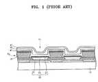
- FIG. 1is a cross-sectional view of a conventional flat panel display device, for example, an organic electro-luminescence display panel disclosed in Japanese Patent Publication No. 2001-284041.
- an emission element 20is formed between partition walls 31 which are extruded on a substrate 11 .
- the emission element 20includes a first electrode layer 21 as anode injecting holes, an organic film 23 in which light is emitted by the recombination of holes and electrons, and a second electrode layer 27 as cathode injecting electrons.
- the organic film 23light is emitted by the recombination of holes injected from the first electrode layer 21 and electrons injected from the second electrode layer 27 , respectively.
- the first electrode layer 21be formed of a material having a high work function and the second electrode layer 27 be formed of material having a low work function.
- the second electrode layer 27is highly active and has instable chemical characteristics, and therefore can be easily oxidized or corroded if exposed to outside moisture or oxygen.
- the organic film 23 having an emission layeralso has a degradation of emission due to a change of crystalline structure when moisture or oxygen permeates. In an extreme case, dark spots are formed thereby losing a display function. Therefore, in the conventional art, in order to isolate the organic film 23 and the second electrode layer 27 from the outside, first and second inorganic passivation layers 41 formed of an inorganic compound and a resin capsulation layer 45 therebetween are formed.
- the permeation of oxygen/moisture through a main face of the first and second passivation layers 41e.g., the permeation of harmful material via a path R 1 is effectively prevented.
- the penetration of harmful material through the side of the exposed first and second passivation layers 41e.g., the permeation via a path R 2 is not effectively prevented.
- the present inventionprovides a flat panel display device blocking permeation of harmful material such as moisture or oxygen, thereby preventing degradation of performance of the flat panel display device over a period of time.
- the present inventionalso provides a flat panel display device having an improved structure requiring minimal additional processing or additional manufacturing cost.
- a flat panel display devicehaving a display area in which a desired image is displayed, and a non-display area arranged outside the display area, the display device includes: bank portions arranged on a first substrate in a predetermined pattern in the display area and partitioning a plurality of first openings; an emission element arranged at each first opening; dummy bank portions formed in the non-display area together with the bank portions; and a sealing passivation layer covering the emission element, consisting of at least a two-layer structure including an organic film and an inorganic film alternately deposited, arranged along a surface defining the dummy bank portions, and having a sectional portion contacting a main surface of the first substrate or a film on the first substrate.
- the sectional portion of the sealing passivation layeris a terminal end thereof.
- a flat panel display devicehaving a display area in which a desired image is displayed, and a non-display area arranged outside the display area, the display device includes: bank portions arranged on a substrate in a predetermined pattern in the display area and partitioning a plurality of first openings; an emission element arranged at each first opening; dummy bank portions formed in the non-display area together with the bank portions; and a sealing passivation layer covering the emission element, consisting of at least a two-layer structure comprising an organic film and an inorganic film alternately deposited, arranged along a surface defining the dummy bank portions, and having a sectional portion contacting a side surface of the dummy bank portion.
- the sectional portion of the sealing passivation layeris a terminal end thereof.
- FIG. 1is a cross-sectional view of a conventional flat panel display device.
- FIG. 2Ais a plan view illustrating a structure of an exemplary embodiment of a flat panel display device according to the present invention
- FIG. 2Bis an enlarged circled portion of FIG. 2A illustrating a plurality of subpixels of each unit pixel arranged in an array;
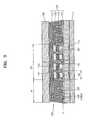
- FIG. 3is a cross-sectional view of the exemplary embodiment of the flat panel display device of FIG. 2 taken along line III-III indicated in FIG. 2 , according to the present invention
- FIG. 4is an enlarged partial perspective view of the exemplary embodiment of the flat panel display device of FIG. 2 showing bank portions and dummy bank portions illustrated in FIG. 3 , according to the present invention
- FIGS. 5 and 6are enlarged partial perspective views of the flat panel display device of FIG. 2 showing modified bank portions and dummy banks portion according to exemplary embodiments of the present invention.
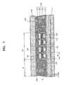
- FIG. 7is a cross-sectional view of another exemplary embodiment of a flat panel display device according to the present invention.
- first, second, third, and the likemay be used herein to describe various elements, components, regions, layers and/or sections, these elements, components, regions, layers and/or sections should not be limited by these terms. These terms are only used to distinguish one element, component, region, layer or section from another element, component, region, layer or section. Thus, a first element, component, region, layer or section discussed below could be termed a second element, component, region, layer or section without departing from the teachings of the present invention.
- spatially relative termssuch as “beneath”, “below”, “lower”, “above”, “upper” and the like, may be used herein for ease of description to describe one element or feature's relationship to another element(s) or feature(s) as illustrated in the figures. It will be understood that the spatially relative terms are intended to encompass different orientations of the device in use or operation in addition to the orientation depicted in the figures. For example, if the device in the figures is turned over, elements described as “below” or “beneath” other elements or features would then be oriented “above” the other elements or features. Thus, the exemplary term “below” can encompass both an orientation of above and below. The device may be otherwise oriented (rotated 90 degrees or at other orientations) and the spatially relative descriptors used herein interpreted accordingly.
- FIG. 2Ais a plan view of a structure of a flat panel display device according to an embodiment of the present invention.
- FIG. 2Bis an enlarged circled portion of FIG. 2A illustrating a plurality of subpixels of each unit pixel arranged in an array.
- the flat panel display deviceincludes a display area (DP), which is where a desired image is displayed, and a non-display area outside the display area DP having a desired width W along the border of the display area DP.
- a plurality of subpixels SPare arranged in an array.
- Each subpixel SPis classified as either a red subpixel (R), a green subpixel (G) or a blue subpixel (B) according to an emission color of the subpixel SP.
- a unit pixelconsists of a red subpixel R, a green subpixel G and a blue subpixel B and each subpixel SP includes an emission element (referred to as an “organic EL element”) having a corresponding emission color, where “EL” stands for electro luminescence.
- the non-display areais provided along the outer border region of the display area DP to protect the display area DP.
- the non-display areais also provided with a dummy bank portion preventing permeation of harmful material.
- FIG. 3is a cross-sectional view of the exemplary embodiment of the flat panel display device of FIG. 2 taken along line III-III indicated in FIG. 2 , according to the present invention.
- the display area DPis provided with bank portions 131 partitioning a plurality of organic EL elements 120 .
- Each organic EL element 120forms a light-emitting area which acts independently in electric and optical operation as separated from each other by the bank portions 131 .
- Each organic EL element 120includes a first electrode 121 and a second electrode 127 , and an organic film inserted between the first and second electrodes 121 and 127 .
- the organic filmincludes an emission layer 123 and a hole injecting layer 125 .
- the organic filmmay have a stacked structure of a hole injection layer (“HIL”), a hole transport layer (“HTL”), an emission layer (“EML”), an electron injection layer (“EIL”) and an electron transport layer (“ETL”) or a combination thereof. Also, the organic film may have a stacked structure of a hole transport layer (“HTL”) and an emission layer (“EML”).
- the structure of the organic filmis not limited to the structures described above, and may be formed of a single emission layer or two layers comprising a hole transport layer and the emission layer or two layers comprising the emission layer and the electron transport layer, for example.
- the emission layer 123is classified as either a red emission layer, a green emission layer or a blue emission layer according to emission color.
- the first electrode 121 and the second electrode 127function as a cathode and an anode, respectively.
- the first electrode 121may be formed commonly to the organic EL elements 120 and the second electrode 127 may be formed independently of each organic EL element 120 .
- the flat panel display device according to the current exemplary embodiment of the present inventionis a top emission type and it is desirable for effective light extraction therefrom to make the second electrode 127 formed of a transparent electrode material.
- the transparent electrode material used to form the second electrode 127includes, for example, indium tin oxide (“ITO”), indium zinc oxide (“IZO”), and other similar transparent electrode materials.
- ITOindium tin oxide
- IZOindium zinc oxide
- It is desirable that the first electrode 121is formed of a metal film having good light reflective properties, such as Al or Ag, to reflect a downward injecting display light from the emission layer 123 upwards.
- the flat panel display deviceis an active matrix display device containing thin film transistors (“TFTs”) such as switching TFTs, driving TFTs, etc. and capacitors may be included in a TFT layer 115 deposited under the organic EL element 120 .
- TFTsthin film transistors
- the number or the type of the TFTsis not limited to the above described examples.
- a switching TFTdetects an on/off condition of the corresponding organic EL element 120 and a driving TFT controls the current applied to the organic EL element 120 according to a signal from the switching TFT.
- the second electrode 127is electrically connected to the drain electrode of the driving TFT and a driving current is applied to a corresponding organic EL element 120 through the second electrode 127 .
- FIG. 4is an enlarged partial perspective view of the exemplary embodiment of the flat panel display device of FIG. 2 showing bank portions 131 and dummy bank portions 135 illustrated in FIG. 3 , according to the present invention.
- the bank portions 131 partitioning a plurality of first openings 120 ′are formed in a predetermined matrix formation and the emission layer 123 , the hole injection layer 125 and the second electrode 127 are laminated successively in the first openings 120 ′.
- the emission layer 123 , the hole injection layer 125 and the second electrode 127are laminated successively on the first electrode 121 exposed through the first opening 120 ′.
- the dummy bank portions 135are provided in the non-display area.
- the bank portions 131 and the dummy bank portions 135 integrated theretoare formed according to the following process.
- a raw material paste of the bank portions 131 on a first substrate 111 in which a TFT layer 115 and the first electrode 121 are formede.g., coating polymer resin material such as polyvinyl acetate (“PVA”) over the whole surface of the first substrate 111 including the display area DP and the non-display area, by forming the predetermined matrix pattern in both the display area and the non-display area, the bank portions 131 and the dummy bank portions 135 integrated thereto are obtained simultaneously.
- PVApolyvinyl acetate
- the dummy bank portions 135perform a shielding function preventing permeation of harmful material such as oxygen and moisture which oxidize and corrode the emission layer 123 or the first and second electrodes 121 and 127 of the organic EL element 120 .
- the present inventionuses a conventional process for forming the bank portions 131 in the display area DP for forming the display bank portions 135 functioning as a shield barrier so that additional processes are not necessary and costs are minimized.
- the dummy bank portions 135include dummy banks 135 a arranged with the second openings 135 ′ defined between adjacent dummy banks 135 a . It may be effective to locate at least two dummy banks 135 a in series for preventing permeation of harmful elements.
- a sealing passivation layer 140is provided to prevent permeation of moisture and oxygen into the organic EL element 120 .
- the sealing passivation layer 140may have at least two films having a blocking ability to prevent harmful material from permeating to the organic EL element 120 .
- the sealing passivation layer 140has at least one organic film 141 and one inorganic film 145 .
- the sealing passivation layer 140With exposure to outside oxygen or moisture (as the harmful material), the sealing passivation layer 140 has a function of preventing the inner films from being oxidized and corroded with the harmful material. That is, the sealing passivation layer 140 isolates the first and second electrodes 121 and 127 , as well as isolating the emission layer 123 of the organic EL element 120 from the harmful material.
- the sealing passivation layer 140is formed not only in the display area DP in which the organic EL element 120 is located, but also in the non-display area.
- the sealing passivation layer 140 in the non-display areais formed in a corrugated shape along the dummy bank portions 135 , as illustrated in FIG. 3 . The corrugated shape results from the sealing passivation layer 140 filling the second openings 135 ′ defined between adjacent dummy banks 135 a.
- the sealing passivation layer 140is constructed in a laminated structure of the organic film 141 /inorganic film 145 having different material characteristics so that the resistance to permeation of moisture or oxygen is increased and at least, the permeation rate is quite retarded near the interface of the organic film 141 /inorganic film 145 .
- the organic film 141may be formed of a high molecular organic film, for example, polyacrylate, polyurea, polyester, polyethylene, polypropylene, methacrylic, acrylic, and derivatives thereof or a small molecular weight organic film, for example, but is not limited thereto.
- the inorganic film 145 deposited on the organic film 141may be formed of oxide, carbide and nitride of silicon, for example SiO 2 , SiC, SiN, SiON or In 2 O 3 , TiO 2 , Al 2 O 3 .
- the multi-layered sealing passivation layer 140Due to the multi-layered sealing passivation layer 140 , permeation of harmful material through a main surface, e.g., the upright permeation of the sealing passivation layer 140 is substantially prevented. However, in spite of the multi-layered structure, harmful material may still permeate along the organic film 141 or the inorganic film 145 after entering through a sectional portion S of the sealing passivation layer 140 . In the present invention, permeation of harmful material through the sectional portion S may be prevented by not exposing the cross section of the sealing passivation layer 140 to the outside.
- the sectional portion S of the sealing passivation layer 140contacts the first electrode 121 structurally preventing contact between the sectional portions S of the sealing passivation layer 140 and the harmful material, such as oxygen and/or moisture.
- the sectional portion S of the sealing passivation layeris a terminal end thereof.
- the sealing passivation layer 140 formed at the non-display areais coated on the dummy bank portions 135 and has a corrugated shape.
- the filling member coated on the sealing passivation layer 140is filled on the concave portion of the corrugated shape and functions as a planarization layer to make a planar surface.
- a second substrate 150 arranged on the sealing passivation layer 140may be tightly attached to the planar surface of the sealing passivation layer 140 without having a gap therebetween.
- an interfacing film directly contacting the organic EL element 120may consist of the organic film 141 or the inorganic film 145 according to a depositing order. However, it is preferable that the interfacing film is the organic film 141 directly contacting the organic EL element 120 due to its planarization effect.
- the bank portions 131 and the dummy bank portions 135are formed in a matrix pattern and the openings 120 ′ and 135 ′, respectively, partitioned by them are arranged in parallel along one direction and are arranged perpendicular to the one direction.
- the scope of the present inventionis not limited to the pattern of the bank portions 131 and the dummy bank portions 135 , and for example, the openings 120 ′ and 135 ′ partitioned by the bank portions 131 and the dummy bank portions 135 shown in FIG. 5 are arranged in parallel along one direction but they are arranged in a zigzag formation along a perpendicular direction to the one direction.
- the openings 120 ′ and 135 ′ partitioned by the bank portions 131 and the dummy bank portion 135 shown in FIG. 6have a hexagonal honey comb structure and various other polygonal shapes of the bank portions 131 and the dummy bank portions 135 may be provided in alternative exemplary embodiments of the present invention.
- like reference numerals in the drawingsdenote like elements as previously described.
- FIG. 7is a cross-sectional view of another exemplary embodiment of a flat panel display device according to the present invention.
- a light-emitting element 120is arranged in the display area DP and the organic EL element 120 includes films 123 , 125 and 127 sequentially deposited in a first opening 120 ′ partitioned by bank portions 131 . Since the organic light-emitting element 120 is sealed from the outside by a sealing passivation layer 140 , the inner film of the organic EL element 120 is prevented from being oxidized and corroded.
- the sealing passivation layer 140is formed in a corrugated shape over the non-display area along dummy bank portions 135 filling second openings 135 ′.
- a sectional portion S of the sealing passivation layer 140contacts slanted surfaces defining the dummy bank portions 135 .
- the dummy bank portions 135include dummy banks 135 a arranged with the second openings 135 ′.
- the sectional portion S of the sealing passivation layer 140contacts the slanted surfaces defining the dummy banks 135 a arranged at the outermost location. Thus, permeation of harmful material through the sectional portion S is prevented.
- the sealing passivation layer 140is formed by sequentially depositing raw material paste of the organic film 141 and the inorganic film 145 . It is difficult to precisely control the end points of the organic film 141 and the inorganic film 145 according to processing characteristics. That is, it is desirable that the location of forming the sectional portion S is controlled so as to not expose the sectional portion S of the sealing passivation layer 140 , and thus, controlling of the end point of the films 141 and 145 is required. In order to stop a nozzle which is continuously ejecting the raw material paste and moving in one direction at a precise location, a stopping location of the nozzle and halting ejection of the raw material needs to be controlled very precisely.
- the dummy bank portions 135 a located at an outside edgefunction as stoppers to the nozzle.
- the flow of the paste ejected from the nozzlecan be stopped smoothly and the sectional portion S of the sealing passivation layer 140 is formed by contacting the dummy bank portions 135 a .
- permeation of harmful material through the sectional portion Smay be prevented.
- a sealing member 160may be arranged between the dummy banks 135 a located at the outermost position and the second substrate 150 .
- the sealing member 160may be formed using a hardening process after inserting a liquid sealant between the dummy banks 135 a and the second substrate 150 . It is desired that at least two dummy banks 135 a are located with the second opening 135 ′ therebetween continuously and overlapping each other since the dummy bank portions 135 function as a blocking member to prevent permeation of outside harmful material.
- the active matrix flat panel display device controlling an input signal per pixel using the thin film transistors (“TFTs”)is described as an exemplary embodiment of the present invention, but the present invention is not limited to the driving method.
- the present inventionmay be applied to the passive matrix flat panel display device.
- the inner portion of the display deviceis reliably sealed. Especially, the sectional portion of the sealing member is not exposed to the outside so as to prevent permeation of harmful material. Thus, formation of a dark spot resulting in a loss of its display function and brightness is prevented.
- the flat panel display device of the present inventionby using a conventional process to form the bank portions in the display area, the dummy banks are formed together with the bank portions to prevent harmful materials from permeating, and thus additional manufacturing processes or additional manufacturing costs may be minimized.
Landscapes
- Chemical & Material Sciences (AREA)
- Inorganic Chemistry (AREA)
- Optics & Photonics (AREA)
- Physics & Mathematics (AREA)
- Engineering & Computer Science (AREA)
- Microelectronics & Electronic Packaging (AREA)
- General Health & Medical Sciences (AREA)
- Public Health (AREA)
- Veterinary Medicine (AREA)
- Animal Behavior & Ethology (AREA)
- Life Sciences & Earth Sciences (AREA)
- Health & Medical Sciences (AREA)
- Electroluminescent Light Sources (AREA)
Abstract
Description
- This application claims priority to Korean Patent Application No. 10-2006-0003118, filed on Jan. 11, 2006, and all the benefits accruing therefrom under 35 U.S.C. § 119, the contents of which in its entirety are herein incorporated by reference.
- 1. Field of the Invention
- The present invention relates to a flat panel display device, and in particular, to a flat panel display device with an improved structure which prevents permeation of harmful material such as moisture or oxygen and degradation of performance of the flat panel display device.
- 2. Description of the Related Art
FIG. 1 is a cross-sectional view of a conventional flat panel display device, for example, an organic electro-luminescence display panel disclosed in Japanese Patent Publication No. 2001-284041. Referring toFIG. 1 , anemission element 20 is formed betweenpartition walls 31 which are extruded on asubstrate 11. Theemission element 20 includes afirst electrode layer 21 as anode injecting holes, anorganic film 23 in which light is emitted by the recombination of holes and electrons, and asecond electrode layer 27 as cathode injecting electrons. In theorganic film 23, light is emitted by the recombination of holes injected from thefirst electrode layer 21 and electrons injected from thesecond electrode layer 27, respectively. To this end, it is preferable that thefirst electrode layer 21 be formed of a material having a high work function and thesecond electrode layer 27 be formed of material having a low work function. Thesecond electrode layer 27 is highly active and has instable chemical characteristics, and therefore can be easily oxidized or corroded if exposed to outside moisture or oxygen. Theorganic film 23 having an emission layer also has a degradation of emission due to a change of crystalline structure when moisture or oxygen permeates. In an extreme case, dark spots are formed thereby losing a display function. Therefore, in the conventional art, in order to isolate theorganic film 23 and thesecond electrode layer 27 from the outside, first and secondinorganic passivation layers 41 formed of an inorganic compound and aresin capsulation layer 45 therebetween are formed. Since the first and secondinorganic passivation layers 41 are stacked over theemission element 20, the permeation of oxygen/moisture through a main face of the first andsecond passivation layers 41, e.g., the permeation of harmful material via a path R1 is effectively prevented. However, the penetration of harmful material through the side of the exposed first andsecond passivation layers 41, e.g., the permeation via a path R2 is not effectively prevented.- The present invention provides a flat panel display device blocking permeation of harmful material such as moisture or oxygen, thereby preventing degradation of performance of the flat panel display device over a period of time.
- The present invention also provides a flat panel display device having an improved structure requiring minimal additional processing or additional manufacturing cost.
- According to an exemplary embodiment of the present invention, there is provided a flat panel display device having a display area in which a desired image is displayed, and a non-display area arranged outside the display area, the display device includes: bank portions arranged on a first substrate in a predetermined pattern in the display area and partitioning a plurality of first openings; an emission element arranged at each first opening; dummy bank portions formed in the non-display area together with the bank portions; and a sealing passivation layer covering the emission element, consisting of at least a two-layer structure including an organic film and an inorganic film alternately deposited, arranged along a surface defining the dummy bank portions, and having a sectional portion contacting a main surface of the first substrate or a film on the first substrate. The sectional portion of the sealing passivation layer is a terminal end thereof.
- According to another exemplary embodiment of the present invention, there is provided a flat panel display device having a display area in which a desired image is displayed, and a non-display area arranged outside the display area, the display device includes: bank portions arranged on a substrate in a predetermined pattern in the display area and partitioning a plurality of first openings; an emission element arranged at each first opening; dummy bank portions formed in the non-display area together with the bank portions; and a sealing passivation layer covering the emission element, consisting of at least a two-layer structure comprising an organic film and an inorganic film alternately deposited, arranged along a surface defining the dummy bank portions, and having a sectional portion contacting a side surface of the dummy bank portion. The sectional portion of the sealing passivation layer is a terminal end thereof.
- The above and other aspects, features and advantages of the present invention will become more apparent by describing in more detail exemplary embodiments thereof with reference to the attached drawings in which:
FIG. 1 is a cross-sectional view of a conventional flat panel display device.FIG. 2A is a plan view illustrating a structure of an exemplary embodiment of a flat panel display device according to the present invention;FIG. 2B is an enlarged circled portion ofFIG. 2A illustrating a plurality of subpixels of each unit pixel arranged in an array;FIG. 3 is a cross-sectional view of the exemplary embodiment of the flat panel display device ofFIG. 2 taken along line III-III indicated inFIG. 2 , according to the present invention;FIG. 4 is an enlarged partial perspective view of the exemplary embodiment of the flat panel display device ofFIG. 2 showing bank portions and dummy bank portions illustrated inFIG. 3 , according to the present inventionFIGS. 5 and 6 are enlarged partial perspective views of the flat panel display device ofFIG. 2 showing modified bank portions and dummy banks portion according to exemplary embodiments of the present invention; andFIG. 7 is a cross-sectional view of another exemplary embodiment of a flat panel display device according to the present invention.- The present invention will now be described more fully hereinafter with reference to the accompanying drawings, in which exemplary embodiments of the present invention are shown. This invention may, however, be embodied in many different forms and should not be construed as limited to the exemplary embodiments set forth herein. Rather, these exemplary embodiments are provided so that this disclosure will be thorough and complete, and will fully convey the scope of the invention to those skilled in the art. Like reference numerals refer to like elements throughout.
- It will be understood that when an element is referred to as being “on” another element, it can be directly on the other element or intervening elements may be present therebetween. In contrast, when an element is referred to as being “directly on” another element, there are no intervening elements present. As used herein, the term “and/or” includes any and all combinations of one or more of the associated listed items.
- It will be understood that, although the terms first, second, third, and the like may be used herein to describe various elements, components, regions, layers and/or sections, these elements, components, regions, layers and/or sections should not be limited by these terms. These terms are only used to distinguish one element, component, region, layer or section from another element, component, region, layer or section. Thus, a first element, component, region, layer or section discussed below could be termed a second element, component, region, layer or section without departing from the teachings of the present invention.
- The terminology used herein is for the purpose of describing particular embodiments only and is not intended to be limiting of the invention. As used herein, the singular forms “a”, “an” and “the” are intended to include the plural forms as well, unless the context clearly indicates otherwise. It will be further understood that the terms “comprises” and/or “comprising,” or “includes” and/or “including” when used in this specification, specify the presence of stated features, regions, integers, steps, operations, elements, and/or components, but do not preclude the presence or addition of one or more other features, regions, integers, steps, operations, elements, components, and/or groups thereof.
- Spatially relative terms, such as “beneath”, “below”, “lower”, “above”, “upper” and the like, may be used herein for ease of description to describe one element or feature's relationship to another element(s) or feature(s) as illustrated in the figures. It will be understood that the spatially relative terms are intended to encompass different orientations of the device in use or operation in addition to the orientation depicted in the figures. For example, if the device in the figures is turned over, elements described as “below” or “beneath” other elements or features would then be oriented “above” the other elements or features. Thus, the exemplary term “below” can encompass both an orientation of above and below. The device may be otherwise oriented (rotated 90 degrees or at other orientations) and the spatially relative descriptors used herein interpreted accordingly.
- Unless otherwise defined, all terms (including technical and scientific terms) used herein have the same meaning as commonly understood by one of ordinary skill in the art to which this invention belongs. It will be further understood that terms, such as those defined in commonly used dictionaries, should be interpreted as having a meaning that is consistent with their meaning in the context of the relevant art and the present disclosure, and will not be interpreted in an idealized or overly formal sense unless expressly so defined herein.
- Hereinafter, the present invention will be described in more detail by explaining exemplary embodiments of the present invention with reference to the attached drawings.
FIG. 2A is a plan view of a structure of a flat panel display device according to an embodiment of the present invention.FIG. 2B is an enlarged circled portion ofFIG. 2A illustrating a plurality of subpixels of each unit pixel arranged in an array. Referring toFIGS. 2A and 2B , the flat panel display device includes a display area (DP), which is where a desired image is displayed, and a non-display area outside the display area DP having a desired width W along the border of the display area DP. In the display area DP, a plurality of subpixels SP are arranged in an array. Each subpixel SP is classified as either a red subpixel (R), a green subpixel (G) or a blue subpixel (B) according to an emission color of the subpixel SP. A unit pixel consists of a red subpixel R, a green subpixel G and a blue subpixel B and each subpixel SP includes an emission element (referred to as an “organic EL element”) having a corresponding emission color, where “EL” stands for electro luminescence. As will be described below, the non-display area is provided along the outer border region of the display area DP to protect the display area DP. The non-display area is also provided with a dummy bank portion preventing permeation of harmful material.FIG. 3 is a cross-sectional view of the exemplary embodiment of the flat panel display device ofFIG. 2 taken along line III-III indicated inFIG. 2 , according to the present invention. The display area DP is provided withbank portions 131 partitioning a plurality oforganic EL elements 120. Eachorganic EL element 120 forms a light-emitting area which acts independently in electric and optical operation as separated from each other by thebank portions 131. Eachorganic EL element 120 includes afirst electrode 121 and asecond electrode 127, and an organic film inserted between the first andsecond electrodes FIG. 3 , the organic film includes anemission layer 123 and ahole injecting layer 125. The organic film may have a stacked structure of a hole injection layer (“HIL”), a hole transport layer (“HTL”), an emission layer (“EML”), an electron injection layer (“EIL”) and an electron transport layer (“ETL”) or a combination thereof. Also, the organic film may have a stacked structure of a hole transport layer (“HTL”) and an emission layer (“EML”). The structure of the organic film is not limited to the structures described above, and may be formed of a single emission layer or two layers comprising a hole transport layer and the emission layer or two layers comprising the emission layer and the electron transport layer, for example.- The
emission layer 123 is classified as either a red emission layer, a green emission layer or a blue emission layer according to emission color. - The
first electrode 121 and thesecond electrode 127 function as a cathode and an anode, respectively. Thefirst electrode 121 may be formed commonly to theorganic EL elements 120 and thesecond electrode 127 may be formed independently of eachorganic EL element 120. The flat panel display device according to the current exemplary embodiment of the present invention is a top emission type and it is desirable for effective light extraction therefrom to make thesecond electrode 127 formed of a transparent electrode material. The transparent electrode material used to form thesecond electrode 127 includes, for example, indium tin oxide (“ITO”), indium zinc oxide (“IZO”), and other similar transparent electrode materials. It is desirable that thefirst electrode 121 is formed of a metal film having good light reflective properties, such as Al or Ag, to reflect a downward injecting display light from theemission layer 123 upwards. - The flat panel display device according to the current exemplary embodiment is an active matrix display device containing thin film transistors (“TFTs”) such as switching TFTs, driving TFTs, etc. and capacitors may be included in a
TFT layer 115 deposited under theorganic EL element 120. The number or the type of the TFTs is not limited to the above described examples. For example, a switching TFT detects an on/off condition of the correspondingorganic EL element 120 and a driving TFT controls the current applied to theorganic EL element 120 according to a signal from the switching TFT. Thesecond electrode 127 is electrically connected to the drain electrode of the driving TFT and a driving current is applied to a correspondingorganic EL element 120 through thesecond electrode 127. FIG. 4 is an enlarged partial perspective view of the exemplary embodiment of the flat panel display device ofFIG. 2 showingbank portions 131 anddummy bank portions 135 illustrated inFIG. 3 , according to the present invention. In the display area DP, thebank portions 131 partitioning a plurality offirst openings 120′ are formed in a predetermined matrix formation and theemission layer 123, thehole injection layer 125 and thesecond electrode 127 are laminated successively in thefirst openings 120′. In particular, theemission layer 123, thehole injection layer 125 and thesecond electrode 127 are laminated successively on thefirst electrode 121 exposed through thefirst opening 120′.- In the non-display area, the
dummy bank portions 135 are provided. The same pattern as that of thebank portions 131 in the display area DP, e.g., the matrix pattern, extends to the outside of the display area DP and a plurality ofsecond openings 135′ are segmented by thedummy bank portions 135. A sealing passivation layer as will be described below fills thesecond openings 135′. Thebank portions 131 and thedummy bank portions 135 integrated thereto are formed according to the following process. That is, after coating a raw material paste of thebank portions 131 on afirst substrate 111 in which aTFT layer 115 and thefirst electrode 121 are formed, e.g., coating polymer resin material such as polyvinyl acetate (“PVA”) over the whole surface of thefirst substrate 111 including the display area DP and the non-display area, by forming the predetermined matrix pattern in both the display area and the non-display area, thebank portions 131 and thedummy bank portions 135 integrated thereto are obtained simultaneously. - The
dummy bank portions 135 perform a shielding function preventing permeation of harmful material such as oxygen and moisture which oxidize and corrode theemission layer 123 or the first andsecond electrodes organic EL element 120. Compared with conventional techniques requiring an additional process and cost for manufacturing, a partitioning wall to prevent the permeation of harmful material, the present invention uses a conventional process for forming thebank portions 131 in the display area DP for forming thedisplay bank portions 135 functioning as a shield barrier so that additional processes are not necessary and costs are minimized. Thedummy bank portions 135 includedummy banks 135aarranged with thesecond openings 135′ defined between adjacentdummy banks 135a. It may be effective to locate at least twodummy banks 135ain series for preventing permeation of harmful elements. - Referring to
FIG. 3 , on the upper surface of theorganic EL element 120, a sealingpassivation layer 140 is provided to prevent permeation of moisture and oxygen into theorganic EL element 120. The sealingpassivation layer 140 may have at least two films having a blocking ability to prevent harmful material from permeating to theorganic EL element 120. In this case, the sealingpassivation layer 140 has at least oneorganic film 141 and oneinorganic film 145. - With exposure to outside oxygen or moisture (as the harmful material), the sealing
passivation layer 140 has a function of preventing the inner films from being oxidized and corroded with the harmful material. That is, the sealingpassivation layer 140 isolates the first andsecond electrodes emission layer 123 of theorganic EL element 120 from the harmful material. The sealingpassivation layer 140 is formed not only in the display area DP in which theorganic EL element 120 is located, but also in the non-display area. The sealingpassivation layer 140 in the non-display area is formed in a corrugated shape along thedummy bank portions 135, as illustrated inFIG. 3 . The corrugated shape results from the sealingpassivation layer 140 filling thesecond openings 135′ defined between adjacentdummy banks 135a. - The sealing
passivation layer 140 is constructed in a laminated structure of theorganic film 141/inorganic film 145 having different material characteristics so that the resistance to permeation of moisture or oxygen is increased and at least, the permeation rate is quite retarded near the interface of theorganic film 141/inorganic film 145. Theorganic film 141 may be formed of a high molecular organic film, for example, polyacrylate, polyurea, polyester, polyethylene, polypropylene, methacrylic, acrylic, and derivatives thereof or a small molecular weight organic film, for example, but is not limited thereto. Also, theinorganic film 145 deposited on theorganic film 141 may be formed of oxide, carbide and nitride of silicon, for example SiO2, SiC, SiN, SiON or In2O3, TiO2, Al2O3. - Due to the multi-layered
sealing passivation layer 140, permeation of harmful material through a main surface, e.g., the upright permeation of the sealingpassivation layer 140 is substantially prevented. However, in spite of the multi-layered structure, harmful material may still permeate along theorganic film 141 or theinorganic film 145 after entering through a sectional portion S of the sealingpassivation layer 140. In the present invention, permeation of harmful material through the sectional portion S may be prevented by not exposing the cross section of the sealingpassivation layer 140 to the outside. In an exemplary embodiment of the present invention, the sectional portion S of the sealingpassivation layer 140 contacts thefirst electrode 121 structurally preventing contact between the sectional portions S of the sealingpassivation layer 140 and the harmful material, such as oxygen and/or moisture. The sectional portion S of the sealing passivation layer is a terminal end thereof. - The sealing
passivation layer 140 formed at the non-display area is coated on thedummy bank portions 135 and has a corrugated shape. The filling member coated on the sealingpassivation layer 140 is filled on the concave portion of the corrugated shape and functions as a planarization layer to make a planar surface. Thus, asecond substrate 150 arranged on the sealingpassivation layer 140 may be tightly attached to the planar surface of the sealingpassivation layer 140 without having a gap therebetween. - In the sealing
passivation layer 140, an interfacing film directly contacting theorganic EL element 120 may consist of theorganic film 141 or theinorganic film 145 according to a depositing order. However, it is preferable that the interfacing film is theorganic film 141 directly contacting theorganic EL element 120 due to its planarization effect. - Referring to
FIG. 4 , thebank portions 131 and thedummy bank portions 135 are formed in a matrix pattern and theopenings 120′ and135′, respectively, partitioned by them are arranged in parallel along one direction and are arranged perpendicular to the one direction. The scope of the present invention is not limited to the pattern of thebank portions 131 and thedummy bank portions 135, and for example, theopenings 120′ and135′ partitioned by thebank portions 131 and thedummy bank portions 135 shown inFIG. 5 are arranged in parallel along one direction but they are arranged in a zigzag formation along a perpendicular direction to the one direction. Theopenings 120′ and135′ partitioned by thebank portions 131 and thedummy bank portion 135 shown inFIG. 6 have a hexagonal honey comb structure and various other polygonal shapes of thebank portions 131 and thedummy bank portions 135 may be provided in alternative exemplary embodiments of the present invention. In the modified exemplary embodiments shown inFIGS. 5 and 6 , like reference numerals in the drawings denote like elements as previously described. FIG. 7 is a cross-sectional view of another exemplary embodiment of a flat panel display device according to the present invention. Like reference numerals in the drawings denote like elements as previously described. Referring toFIG. 7 , a light-emittingelement 120 is arranged in the display area DP and theorganic EL element 120 includesfilms first opening 120′ partitioned bybank portions 131. Since the organic light-emittingelement 120 is sealed from the outside by a sealingpassivation layer 140, the inner film of theorganic EL element 120 is prevented from being oxidized and corroded. The sealingpassivation layer 140 is formed in a corrugated shape over the non-display area alongdummy bank portions 135 fillingsecond openings 135′. A sectional portion S of the sealingpassivation layer 140 contacts slanted surfaces defining thedummy bank portions 135. In particular, thedummy bank portions 135 includedummy banks 135aarranged with thesecond openings 135′. The sectional portion S of the sealingpassivation layer 140 contacts the slanted surfaces defining thedummy banks 135aarranged at the outermost location. Thus, permeation of harmful material through the sectional portion S is prevented.- The sealing
passivation layer 140 is formed by sequentially depositing raw material paste of theorganic film 141 and theinorganic film 145. It is difficult to precisely control the end points of theorganic film 141 and theinorganic film 145 according to processing characteristics. That is, it is desirable that the location of forming the sectional portion S is controlled so as to not expose the sectional portion S of the sealingpassivation layer 140, and thus, controlling of the end point of thefilms dummy bank portions 135alocated at an outside edge function as stoppers to the nozzle. By thedummy bank portions 135a, the flow of the paste ejected from the nozzle can be stopped smoothly and the sectional portion S of the sealingpassivation layer 140 is formed by contacting thedummy bank portions 135a. Thus, permeation of harmful material through the sectional portion S may be prevented. - The uppermost surface of the
dummy banks 135alocated at the outermost position may not be covered by the sealingpassivation layer 140 and may be spaced from thesecond substrate 150 by as much as the thickness of the sealingpassivation layer 140. To prevent the permeation of harmful material through this gap, a sealingmember 160 may be arranged between thedummy banks 135alocated at the outermost position and thesecond substrate 150. For example, the sealingmember 160 may be formed using a hardening process after inserting a liquid sealant between thedummy banks 135aand thesecond substrate 150. It is desired that at least twodummy banks 135aare located with thesecond opening 135′ therebetween continuously and overlapping each other since thedummy bank portions 135 function as a blocking member to prevent permeation of outside harmful material. - In the meantime, in the specification, for convenience of explanation, the active matrix flat panel display device controlling an input signal per pixel using the thin film transistors (“TFTs”) is described as an exemplary embodiment of the present invention, but the present invention is not limited to the driving method. Thus, the present invention may be applied to the passive matrix flat panel display device.
- According to the flat panel display device of the present invention, in order to protect the inner emission element of the display device from harmful material such as oxygen and/or moisture, the inner portion of the display device is reliably sealed. Especially, the sectional portion of the sealing member is not exposed to the outside so as to prevent permeation of harmful material. Thus, formation of a dark spot resulting in a loss of its display function and brightness is prevented.
- In particular, according to the flat panel display device of the present invention, by using a conventional process to form the bank portions in the display area, the dummy banks are formed together with the bank portions to prevent harmful materials from permeating, and thus additional manufacturing processes or additional manufacturing costs may be minimized.
- While the present invention has been particularly shown and described with reference to exemplary embodiments thereof, it will be understood by those of ordinary skill in the art that various changes in form and details may be made therein without departing from the spirit and scope of the present invention as defined by the following claims.
Claims (12)
Applications Claiming Priority (2)
| Application Number | Priority Date | Filing Date | Title |
|---|---|---|---|
| KR1020060003118AKR100647339B1 (en) | 2006-01-11 | 2006-01-11 | Flat Panel Display |
| KR10-2006-0003118 | 2006-01-11 |
Publications (2)
| Publication Number | Publication Date |
|---|---|
| US20070159089A1true US20070159089A1 (en) | 2007-07-12 |
| US7667397B2 US7667397B2 (en) | 2010-02-23 |
Family
ID=37712837
Family Applications (1)
| Application Number | Title | Priority Date | Filing Date |
|---|---|---|---|
| US11/622,294Active2028-02-06US7667397B2 (en) | 2006-01-11 | 2007-01-11 | Flat panel display device with at least two-layer sealing passivation layer |
Country Status (2)
| Country | Link |
|---|---|
| US (1) | US7667397B2 (en) |
| KR (1) | KR100647339B1 (en) |
Cited By (33)
| Publication number | Priority date | Publication date | Assignee | Title |
|---|---|---|---|---|
| US20090174322A1 (en)* | 2008-01-04 | 2009-07-09 | Tpo Displays Corp. | Organic light-emitting device and method for forming the same |
| US20120061697A1 (en)* | 2007-01-09 | 2012-03-15 | Dai Nippon Printing Co., Ltd. | Organic light-emitting element, organic light-emitting transistor, and light-emitting display device |
| US20130334959A1 (en)* | 2012-03-02 | 2013-12-19 | Au Optronics Corporation | Organic electroluminescent apparatus |
| US20130341659A1 (en)* | 2012-06-22 | 2013-12-26 | Industrial Technology Research Institute | Display panel |
| TWI423187B (en)* | 2009-09-30 | 2014-01-11 | Innolux Corp | Self-emission flat panel display and alignment system for assembling the same |
| CN103985817A (en)* | 2013-02-07 | 2014-08-13 | 三星显示有限公司 | Organic light emitting diode device and manufacturing method thereof |
| US20150014636A1 (en)* | 2013-07-12 | 2015-01-15 | Samsung Display Co., Ltd. | Organic light-emitting display apparatus and method of manufacturing the same |
| CN104425759A (en)* | 2013-08-27 | 2015-03-18 | 财团法人工业技术研究院 | Organic-inorganic composite film and method for forming the same |
| US20150102326A1 (en)* | 2013-10-15 | 2015-04-16 | Samsung Display Co., Ltd. | Flexible organic light emitting diode display and manufacturing method thereof |
| US20150126681A1 (en)* | 2013-08-27 | 2015-05-07 | Industrial Technology Research Institute | Organic-inorganic composite film and method for manufacturing the same |
| US20150340346A1 (en)* | 2014-05-24 | 2015-11-26 | Chen-Fu Chu | Structure of a semiconductor array |
| JP2016039120A (en)* | 2014-08-11 | 2016-03-22 | 株式会社ジャパンディスプレイ | Organic EL display device |
| US20170012242A1 (en)* | 2015-07-07 | 2017-01-12 | Samsung Display Co., Ltd. | Organic light-emitting display apparatus and manufacturing method of the same |
| US20170012233A1 (en)* | 2014-01-29 | 2017-01-12 | Pioneer Oled Lighting Devices Corporation | Light emitting apparatus |
| CN106469746A (en)* | 2015-08-19 | 2017-03-01 | 三星显示有限公司 | Oganic light-emitting display device and its manufacture method |
| US20170084674A1 (en)* | 2015-04-17 | 2017-03-23 | Boe Technology Group Co., Ltd. | OLED Substrate, Manufacturing Method Thereof, and Display Device |
| CN107170777A (en)* | 2017-04-27 | 2017-09-15 | 上海天马有机发光显示技术有限公司 | Organic electroluminescence display panel and display device |
| CN107210375A (en)* | 2015-12-30 | 2017-09-26 | 深圳市柔宇科技有限公司 | Flexible display screen and flexible display screen preparation method |
| US20170330921A1 (en)* | 2013-09-30 | 2017-11-16 | Samsung Display Co., Ltd. | Display devices and methods of manufacturing display devices |
| US9887385B2 (en)* | 2014-09-03 | 2018-02-06 | Lg Display Co., Ltd. | Organic light emitting diode device and method for manufacturing the same |
| CN108232033A (en)* | 2018-01-08 | 2018-06-29 | 京东方科技集团股份有限公司 | A kind of electroluminescence display panel, its packaging method and display device |
| CN109686855A (en)* | 2018-12-04 | 2019-04-26 | 武汉华星光电半导体显示技术有限公司 | A kind of thin-film packing structure and film encapsulation method |
| CN110400889A (en)* | 2019-07-25 | 2019-11-01 | 云谷(固安)科技有限公司 | The preparation method of display panel, display device and display panel |
| JP2019532326A (en)* | 2016-12-09 | 2019-11-07 | エルジー・ケム・リミテッド | Sealant composition |
| US10547028B2 (en) | 2015-03-09 | 2020-01-28 | Samsung Display Co., Ltd. | Organic light emitting diode device with barrier wall |
| JP2020161498A (en)* | 2013-07-22 | 2020-10-01 | 三星ディスプレイ株式會社Samsung Display Co.,Ltd. | Organic light emitting display apparatus and method of manufacturing the same |
| CN112002738A (en)* | 2020-08-10 | 2020-11-27 | 深圳市华星光电半导体显示技术有限公司 | Display panel, display screen and electronic equipment |
| CN112928141A (en)* | 2019-12-06 | 2021-06-08 | 乐金显示有限公司 | Electroluminescent display device |
| US11302897B2 (en)* | 2017-09-18 | 2022-04-12 | Chengdue Boe Optoelectronics Technology Co., Ltd. | Display panel, preparation method thereof, and display device each having first water oxygen barrier bar with first and second sub-barrier bars separated from each other by gaps that are not aligned |
| US11329110B2 (en)* | 2017-12-27 | 2022-05-10 | Sharp Kabushiki Kaisha | Display device having organic buffer layer between inorganic sealing films and method of manufacturing display device |
| US11380743B2 (en)* | 2020-01-08 | 2022-07-05 | Wuhan China Star Optoelectronics Semiconductor Display Technology Co., Ltd. | OLED display device including a plurality of strip-shaped grooves and manufacturing method thereof |
| US11424270B2 (en)* | 2020-06-02 | 2022-08-23 | Wuhan China Star Optoelectronics Semiconductor Display Technology Co., Ltd. | Flexible display device and manufacturing method thereof |
| US20230354675A1 (en)* | 2021-03-24 | 2023-11-02 | Chengdu Boe Optoelectronics Technology Co., Ltd. | Display Panel and Manufacturing Method Thereof, and Display Device |
Families Citing this family (3)
| Publication number | Priority date | Publication date | Assignee | Title |
|---|---|---|---|---|
| KR101307550B1 (en)* | 2007-12-31 | 2013-09-12 | 엘지디스플레이 주식회사 | Organic Light Emitting Display |
| KR20220140935A (en) | 2021-04-09 | 2022-10-19 | 삼성디스플레이 주식회사 | Display panel |
| KR20240107666A (en)* | 2022-12-30 | 2024-07-09 | 엘지디스플레이 주식회사 | Display device |
Citations (13)
| Publication number | Priority date | Publication date | Assignee | Title |
|---|---|---|---|---|
| US20040124770A1 (en)* | 2002-10-25 | 2004-07-01 | Seiko Epson Corporation | Electro-optical device and electronic apparatus |
| US20040207312A1 (en)* | 2003-01-23 | 2004-10-21 | Seiko Epson Corporation | Manufacturing method for organic electroluminescence device, and electronic device therewith |
| US20050140290A1 (en)* | 2003-12-30 | 2005-06-30 | Lg.Philips Lcd Co., Ltd. | Dual panel type organic electroluminescent device and method for fabricating the same |
| US20050179377A1 (en)* | 2004-02-18 | 2005-08-18 | Seiko Epson Corporation | Organic electroluminescent device and electronic Apparatus |
| US20050189878A1 (en)* | 2004-03-01 | 2005-09-01 | Seiko Epson Corporation | Organic electroluminescent device and electronic apparatus |
| US20050264177A1 (en)* | 2004-01-08 | 2005-12-01 | Jin-Koo Chung | Display device, and method of manufacturing the display device |
| US20060055313A1 (en)* | 2004-09-16 | 2006-03-16 | Bae Sung J | Organic electro luminescence device and fabrication method thereof |
| US20060061268A1 (en)* | 2002-05-28 | 2006-03-23 | Seiko Epson Corporation | Light-emitting device with improved brightness control and narrow frame and electronic apparatus with the light-emitting device |
| US20060273717A1 (en)* | 2005-06-03 | 2006-12-07 | Jian Wang | Electronic device including workpieces and a conductive member therebetween |
| US20070108899A1 (en)* | 2005-11-15 | 2007-05-17 | Samsung Electronics Co., Ltd | Display device and fabricating method thereof |
| US20070159094A1 (en)* | 2006-01-11 | 2007-07-12 | Samsung Electronics Co., Ltd. | Flat panel display device and method thereof |
| US20070159096A1 (en)* | 2006-01-11 | 2007-07-12 | Samsung Electronics Co., Ltd | Flat panel display device and method thereof |
| US20070182314A1 (en)* | 2006-02-03 | 2007-08-09 | Oh Tae-Sik | Organic light emitting display providing ultraviolet ray protection and method of manufacturing same |
Family Cites Families (1)
| Publication number | Priority date | Publication date | Assignee | Title |
|---|---|---|---|---|
| JP4004709B2 (en) | 2000-03-30 | 2007-11-07 | パイオニア株式会社 | Organic electroluminescence display panel and manufacturing method thereof |
- 2006
- 2006-01-11KRKR1020060003118Apatent/KR100647339B1/enactiveActive
- 2007
- 2007-01-11USUS11/622,294patent/US7667397B2/enactiveActive
Patent Citations (13)
| Publication number | Priority date | Publication date | Assignee | Title |
|---|---|---|---|---|
| US20060061268A1 (en)* | 2002-05-28 | 2006-03-23 | Seiko Epson Corporation | Light-emitting device with improved brightness control and narrow frame and electronic apparatus with the light-emitting device |
| US20040124770A1 (en)* | 2002-10-25 | 2004-07-01 | Seiko Epson Corporation | Electro-optical device and electronic apparatus |
| US20040207312A1 (en)* | 2003-01-23 | 2004-10-21 | Seiko Epson Corporation | Manufacturing method for organic electroluminescence device, and electronic device therewith |
| US20050140290A1 (en)* | 2003-12-30 | 2005-06-30 | Lg.Philips Lcd Co., Ltd. | Dual panel type organic electroluminescent device and method for fabricating the same |
| US20050264177A1 (en)* | 2004-01-08 | 2005-12-01 | Jin-Koo Chung | Display device, and method of manufacturing the display device |
| US20050179377A1 (en)* | 2004-02-18 | 2005-08-18 | Seiko Epson Corporation | Organic electroluminescent device and electronic Apparatus |
| US20050189878A1 (en)* | 2004-03-01 | 2005-09-01 | Seiko Epson Corporation | Organic electroluminescent device and electronic apparatus |
| US20060055313A1 (en)* | 2004-09-16 | 2006-03-16 | Bae Sung J | Organic electro luminescence device and fabrication method thereof |
| US20060273717A1 (en)* | 2005-06-03 | 2006-12-07 | Jian Wang | Electronic device including workpieces and a conductive member therebetween |
| US20070108899A1 (en)* | 2005-11-15 | 2007-05-17 | Samsung Electronics Co., Ltd | Display device and fabricating method thereof |
| US20070159094A1 (en)* | 2006-01-11 | 2007-07-12 | Samsung Electronics Co., Ltd. | Flat panel display device and method thereof |
| US20070159096A1 (en)* | 2006-01-11 | 2007-07-12 | Samsung Electronics Co., Ltd | Flat panel display device and method thereof |
| US20070182314A1 (en)* | 2006-02-03 | 2007-08-09 | Oh Tae-Sik | Organic light emitting display providing ultraviolet ray protection and method of manufacturing same |
Cited By (65)
| Publication number | Priority date | Publication date | Assignee | Title |
|---|---|---|---|---|
| US20120061697A1 (en)* | 2007-01-09 | 2012-03-15 | Dai Nippon Printing Co., Ltd. | Organic light-emitting element, organic light-emitting transistor, and light-emitting display device |
| US8231423B2 (en)* | 2008-01-04 | 2012-07-31 | Chimei Innolux Corporation | Organic light-emitting device and method for forming the same |
| US20090174322A1 (en)* | 2008-01-04 | 2009-07-09 | Tpo Displays Corp. | Organic light-emitting device and method for forming the same |
| TWI423187B (en)* | 2009-09-30 | 2014-01-11 | Innolux Corp | Self-emission flat panel display and alignment system for assembling the same |
| US9013099B2 (en)* | 2012-03-02 | 2015-04-21 | Au Optronics Corporation | Organic electroluminescent apparatus |
| US20130334959A1 (en)* | 2012-03-02 | 2013-12-19 | Au Optronics Corporation | Organic electroluminescent apparatus |
| TWI473264B (en)* | 2012-03-02 | 2015-02-11 | Au Optronics Corp | Organic electroluminescent apparatus |
| US8981391B2 (en)* | 2012-06-22 | 2015-03-17 | Industrial Technology Research Institute | Display panel with high transparency |
| US20130341659A1 (en)* | 2012-06-22 | 2013-12-26 | Industrial Technology Research Institute | Display panel |
| US12167623B2 (en) | 2013-02-07 | 2024-12-10 | Samsung Display Co., Ltd. | Display device including two inorganic layers and an outer barrier arranged on a substrate |
| CN103985817A (en)* | 2013-02-07 | 2014-08-13 | 三星显示有限公司 | Organic light emitting diode device and manufacturing method thereof |
| US11696462B2 (en) | 2013-02-07 | 2023-07-04 | Samsung Display Co., Ltd. | Display device including two inorganic layers and an outer barrier arranged on a substrate |
| US9419247B2 (en) | 2013-02-07 | 2016-08-16 | Samsung Display Co., Ltd. | Organic light emitting diode device and manufacturing method thereof |
| US10892442B2 (en) | 2013-02-07 | 2021-01-12 | Samsung Display Co., Ltd. | Display device |
| US10586947B2 (en) | 2013-02-07 | 2020-03-10 | Samsung Display Co., Ltd. | Organic light emitting diode device and display device |
| EP2765627A3 (en)* | 2013-02-07 | 2015-12-30 | Samsung Display Co., Ltd. | Organic light emitting diode device and manufacturing method thereof |
| US10199599B2 (en) | 2013-02-07 | 2019-02-05 | Samsung Display Co., Ltd. | Organic light emitting diode device and manufacturing method thereof |
| US9705107B2 (en) | 2013-02-07 | 2017-07-11 | Samsung Display Co., Ltd. | Organic light emitting diode device and manufacturing method thereof |
| US10903448B2 (en) | 2013-07-12 | 2021-01-26 | Samsung Display Co., Ltd. | Organic light-emitting display apparatus and method of manufacturing the same |
| US10622586B2 (en) | 2013-07-12 | 2020-04-14 | Samsung Display Co., Ltd. | Organic light-emitting display apparatus and method of manufacturing the same |
| US9614180B2 (en)* | 2013-07-12 | 2017-04-04 | Samsung Display Co., Ltd. | Organic light-emitting display apparatus and method of manufacturing the same |
| US20150014636A1 (en)* | 2013-07-12 | 2015-01-15 | Samsung Display Co., Ltd. | Organic light-emitting display apparatus and method of manufacturing the same |
| US10084154B2 (en) | 2013-07-12 | 2018-09-25 | Samsung Display Co., Ltd. | Organic light-emitting display apparatus and method of manufacturing the same |
| JP2020161498A (en)* | 2013-07-22 | 2020-10-01 | 三星ディスプレイ株式會社Samsung Display Co.,Ltd. | Organic light emitting display apparatus and method of manufacturing the same |
| CN104425759A (en)* | 2013-08-27 | 2015-03-18 | 财团法人工业技术研究院 | Organic-inorganic composite film and method for forming the same |
| US20150126681A1 (en)* | 2013-08-27 | 2015-05-07 | Industrial Technology Research Institute | Organic-inorganic composite film and method for manufacturing the same |
| US11289553B2 (en)* | 2013-09-30 | 2022-03-29 | Samsung Display Co., Ltd. | Display devices and methods of manufacturing display devices |
| CN110350017A (en)* | 2013-09-30 | 2019-10-18 | 三星显示有限公司 | The method of display device and manufacture display device |
| US12156435B2 (en) | 2013-09-30 | 2024-11-26 | Samsung Display Co., Ltd. | Display devices and methods of manufacturing display devices |
| US20170330921A1 (en)* | 2013-09-30 | 2017-11-16 | Samsung Display Co., Ltd. | Display devices and methods of manufacturing display devices |
| US9293730B2 (en)* | 2013-10-15 | 2016-03-22 | Samsung Display Co., Ltd. | Flexible organic light emitting diode display and manufacturing method thereof |
| US20150102326A1 (en)* | 2013-10-15 | 2015-04-16 | Samsung Display Co., Ltd. | Flexible organic light emitting diode display and manufacturing method thereof |
| JPWO2015114763A1 (en)* | 2014-01-29 | 2017-03-23 | パイオニアOledライティングデバイス株式会社 | Light emitting device |
| US20170012233A1 (en)* | 2014-01-29 | 2017-01-12 | Pioneer Oled Lighting Devices Corporation | Light emitting apparatus |
| US10910350B2 (en)* | 2014-05-24 | 2021-02-02 | Hiphoton Co., Ltd. | Structure of a semiconductor array |
| US20210125971A1 (en)* | 2014-05-24 | 2021-04-29 | Hiphoton Co., Ltd. | Structure of a semiconductor array |
| US20150340346A1 (en)* | 2014-05-24 | 2015-11-26 | Chen-Fu Chu | Structure of a semiconductor array |
| JP2016039120A (en)* | 2014-08-11 | 2016-03-22 | 株式会社ジャパンディスプレイ | Organic EL display device |
| US10290830B2 (en) | 2014-09-03 | 2019-05-14 | Lg Display Co., Ltd. | Organic light emitting diode device and method for manufacturing the same |
| US9887385B2 (en)* | 2014-09-03 | 2018-02-06 | Lg Display Co., Ltd. | Organic light emitting diode device and method for manufacturing the same |
| US11309525B2 (en) | 2015-03-09 | 2022-04-19 | Samsung Display Co., Ltd. | Organic light emitting diode display device with barrier wall and method of manufacturing the same |
| US10547028B2 (en) | 2015-03-09 | 2020-01-28 | Samsung Display Co., Ltd. | Organic light emitting diode device with barrier wall |
| US12137575B2 (en) | 2015-03-09 | 2024-11-05 | Samsung Display Co., Ltd. | Organic light emitting diode display device with barrier wall and method of manufacturing the same |
| US10403694B2 (en)* | 2015-04-17 | 2019-09-03 | Boe Technology Group Co., Ltd. | OLED substrate comprising corresponding pixel definition layer patterns, manufacturing method thereof, and display device |
| US20170084674A1 (en)* | 2015-04-17 | 2017-03-23 | Boe Technology Group Co., Ltd. | OLED Substrate, Manufacturing Method Thereof, and Display Device |
| US20170012242A1 (en)* | 2015-07-07 | 2017-01-12 | Samsung Display Co., Ltd. | Organic light-emitting display apparatus and manufacturing method of the same |
| US10707443B2 (en)* | 2015-07-07 | 2020-07-07 | Samsung Display Co., Ltd. | Organic light-emitting display apparatus and manufacturing method of the same |
| US11316133B2 (en) | 2015-07-07 | 2022-04-26 | Samsung Display Co., Ltd. | Organic light-emitting display apparatus and manufacturing method of the same |
| CN106469746A (en)* | 2015-08-19 | 2017-03-01 | 三星显示有限公司 | Oganic light-emitting display device and its manufacture method |
| US10559633B2 (en)* | 2015-12-30 | 2020-02-11 | Shenzhen Royole Technologies Co. Ltd. | Flexible display screen and manufacturing method therefor |
| US20180240852A1 (en)* | 2015-12-30 | 2018-08-23 | Shenzhen Royole Technologies Co. Ltd. | Flexible display screen and manufacturing method therefor |
| CN107210375A (en)* | 2015-12-30 | 2017-09-26 | 深圳市柔宇科技有限公司 | Flexible display screen and flexible display screen preparation method |
| JP2019532326A (en)* | 2016-12-09 | 2019-11-07 | エルジー・ケム・リミテッド | Sealant composition |
| CN107170777A (en)* | 2017-04-27 | 2017-09-15 | 上海天马有机发光显示技术有限公司 | Organic electroluminescence display panel and display device |
| US11302897B2 (en)* | 2017-09-18 | 2022-04-12 | Chengdue Boe Optoelectronics Technology Co., Ltd. | Display panel, preparation method thereof, and display device each having first water oxygen barrier bar with first and second sub-barrier bars separated from each other by gaps that are not aligned |
| US11329110B2 (en)* | 2017-12-27 | 2022-05-10 | Sharp Kabushiki Kaisha | Display device having organic buffer layer between inorganic sealing films and method of manufacturing display device |
| CN108232033A (en)* | 2018-01-08 | 2018-06-29 | 京东方科技集团股份有限公司 | A kind of electroluminescence display panel, its packaging method and display device |
| CN109686855A (en)* | 2018-12-04 | 2019-04-26 | 武汉华星光电半导体显示技术有限公司 | A kind of thin-film packing structure and film encapsulation method |
| CN110400889A (en)* | 2019-07-25 | 2019-11-01 | 云谷(固安)科技有限公司 | The preparation method of display panel, display device and display panel |
| CN112928141A (en)* | 2019-12-06 | 2021-06-08 | 乐金显示有限公司 | Electroluminescent display device |
| US11380743B2 (en)* | 2020-01-08 | 2022-07-05 | Wuhan China Star Optoelectronics Semiconductor Display Technology Co., Ltd. | OLED display device including a plurality of strip-shaped grooves and manufacturing method thereof |
| US11424270B2 (en)* | 2020-06-02 | 2022-08-23 | Wuhan China Star Optoelectronics Semiconductor Display Technology Co., Ltd. | Flexible display device and manufacturing method thereof |
| CN112002738A (en)* | 2020-08-10 | 2020-11-27 | 深圳市华星光电半导体显示技术有限公司 | Display panel, display screen and electronic equipment |
| US20230354675A1 (en)* | 2021-03-24 | 2023-11-02 | Chengdu Boe Optoelectronics Technology Co., Ltd. | Display Panel and Manufacturing Method Thereof, and Display Device |
| US12063841B2 (en)* | 2021-03-24 | 2024-08-13 | Chengdu Boe Optoelectronics Technology Co., Ltd. | Display panel and manufacturing method thereof, and display device |
Also Published As
| Publication number | Publication date |
|---|---|
| KR100647339B1 (en) | 2006-11-23 |
| US7667397B2 (en) | 2010-02-23 |
Similar Documents
| Publication | Publication Date | Title |
|---|---|---|
| US7667397B2 (en) | Flat panel display device with at least two-layer sealing passivation layer | |
| US8350467B2 (en) | Flat panel display device and method thereof | |
| US7948176B2 (en) | Flat panel display device and method thereof | |
| KR102576997B1 (en) | Display device and method of manufacturing display device | |
| US7091660B2 (en) | Polymer organic light emitting diode | |
| EP3336898B1 (en) | Organic light emitting display device | |
| KR102000932B1 (en) | Display device and method of manufacturing the same | |
| KR100707210B1 (en) | Organic light emitting display and manufacturing method | |
| KR101004874B1 (en) | Display panel and manufacturing method | |
| CN102474939B (en) | Display panel apparatus and method of fabricating display panel apparatus | |
| KR102555403B1 (en) | Organic Light Emitting Diode Panel and Flexible Display Device Using the Same | |
| US7307382B2 (en) | Flat display device including an overflow barrier | |
| US6774392B2 (en) | Organic light emitting diode and method for producing the same | |
| US7872255B2 (en) | Organic light-emitting device | |
| US11094761B2 (en) | Organic light emitting display device and method of fabricating thereof | |
| KR102794929B1 (en) | Organic light emitting display device and method of fabricating thereof | |
| US11049918B2 (en) | Organic light emitting display device and method of fabricating thereof | |
| US20090315027A1 (en) | Light emitting device and manufacturing method of light emitting device | |
| US20200212134A1 (en) | Organic light-emitting display device and method of fabricating the same | |
| JP2010009746A (en) | Light emitting device and method for manufacturing of light emitting device | |
| JP2009021164A (en) | Display device and method of manufacturing the same | |
| KR102616245B1 (en) | Display device | |
| KR100515465B1 (en) | The organic electro-luminescence device and method for fabricating of the same | |
| CN114078903B (en) | Electroluminescent devices and display devices | |
| KR20110061118A (en) | Manufacturing method of organic light emitting display device |
Legal Events
| Date | Code | Title | Description |
|---|---|---|---|
| AS | Assignment | Owner name:SAMSUNG ELECTRONICS CO., LTD, KOREA, REPUBLIC OF Free format text:ASSIGNMENT OF ASSIGNORS INTEREST;ASSIGNORS:OH, TAE-SIK;KANG, SUNG-KEE;KIM, JUNG-WOO;AND OTHERS;REEL/FRAME:018748/0681 Effective date:20070103 Owner name:SAMSUNG ELECTRONICS CO., LTD,KOREA, REPUBLIC OF Free format text:ASSIGNMENT OF ASSIGNORS INTEREST;ASSIGNORS:OH, TAE-SIK;KANG, SUNG-KEE;KIM, JUNG-WOO;AND OTHERS;REEL/FRAME:018748/0681 Effective date:20070103 | |
| FEPP | Fee payment procedure | Free format text:PAYOR NUMBER ASSIGNED (ORIGINAL EVENT CODE: ASPN); ENTITY STATUS OF PATENT OWNER: LARGE ENTITY | |
| STCF | Information on status: patent grant | Free format text:PATENTED CASE | |
| AS | Assignment | Owner name:SAMSUNG DISPLAY CO., LTD., KOREA, REPUBLIC OF Free format text:ASSIGNMENT OF ASSIGNORS INTEREST;ASSIGNOR:SAMSUNG ELECTRONICS CO., LTD.;REEL/FRAME:029019/0139 Effective date:20120904 | |
| FEPP | Fee payment procedure | Free format text:PAYOR NUMBER ASSIGNED (ORIGINAL EVENT CODE: ASPN); ENTITY STATUS OF PATENT OWNER: LARGE ENTITY Free format text:PAYER NUMBER DE-ASSIGNED (ORIGINAL EVENT CODE: RMPN); ENTITY STATUS OF PATENT OWNER: LARGE ENTITY | |
| FPAY | Fee payment | Year of fee payment:4 | |
| FPAY | Fee payment | Year of fee payment:8 | |
| MAFP | Maintenance fee payment | Free format text:PAYMENT OF MAINTENANCE FEE, 12TH YEAR, LARGE ENTITY (ORIGINAL EVENT CODE: M1553); ENTITY STATUS OF PATENT OWNER: LARGE ENTITY Year of fee payment:12 |