US20070155190A1 - Systems and methods for forming metal oxide layers - Google Patents
Systems and methods for forming metal oxide layersDownload PDFInfo
- Publication number
- US20070155190A1 US20070155190A1US11/711,920US71192007AUS2007155190A1US 20070155190 A1US20070155190 A1US 20070155190A1US 71192007 AUS71192007 AUS 71192007AUS 2007155190 A1US2007155190 A1US 2007155190A1
- Authority
- US
- United States
- Prior art keywords
- substrate
- precursor compound
- deposition
- layer
- oxide layer
- Prior art date
- Legal status (The legal status is an assumption and is not a legal conclusion. Google has not performed a legal analysis and makes no representation as to the accuracy of the status listed.)
- Granted
Links
Images


Classifications
- H—ELECTRICITY
- H10—SEMICONDUCTOR DEVICES; ELECTRIC SOLID-STATE DEVICES NOT OTHERWISE PROVIDED FOR
- H10D—INORGANIC ELECTRIC SEMICONDUCTOR DEVICES
- H10D1/00—Resistors, capacitors or inductors
- H10D1/60—Capacitors
- H10D1/68—Capacitors having no potential barriers
- C—CHEMISTRY; METALLURGY
- C23—COATING METALLIC MATERIAL; COATING MATERIAL WITH METALLIC MATERIAL; CHEMICAL SURFACE TREATMENT; DIFFUSION TREATMENT OF METALLIC MATERIAL; COATING BY VACUUM EVAPORATION, BY SPUTTERING, BY ION IMPLANTATION OR BY CHEMICAL VAPOUR DEPOSITION, IN GENERAL; INHIBITING CORROSION OF METALLIC MATERIAL OR INCRUSTATION IN GENERAL
- C23C—COATING METALLIC MATERIAL; COATING MATERIAL WITH METALLIC MATERIAL; SURFACE TREATMENT OF METALLIC MATERIAL BY DIFFUSION INTO THE SURFACE, BY CHEMICAL CONVERSION OR SUBSTITUTION; COATING BY VACUUM EVAPORATION, BY SPUTTERING, BY ION IMPLANTATION OR BY CHEMICAL VAPOUR DEPOSITION, IN GENERAL
- C23C16/00—Chemical coating by decomposition of gaseous compounds, without leaving reaction products of surface material in the coating, i.e. chemical vapour deposition [CVD] processes
- C23C16/22—Chemical coating by decomposition of gaseous compounds, without leaving reaction products of surface material in the coating, i.e. chemical vapour deposition [CVD] processes characterised by the deposition of inorganic material, other than metallic material
- C23C16/30—Deposition of compounds, mixtures or solid solutions, e.g. borides, carbides, nitrides
- C23C16/40—Oxides
- C23C16/401—Oxides containing silicon
- C—CHEMISTRY; METALLURGY
- C23—COATING METALLIC MATERIAL; COATING MATERIAL WITH METALLIC MATERIAL; CHEMICAL SURFACE TREATMENT; DIFFUSION TREATMENT OF METALLIC MATERIAL; COATING BY VACUUM EVAPORATION, BY SPUTTERING, BY ION IMPLANTATION OR BY CHEMICAL VAPOUR DEPOSITION, IN GENERAL; INHIBITING CORROSION OF METALLIC MATERIAL OR INCRUSTATION IN GENERAL
- C23C—COATING METALLIC MATERIAL; COATING MATERIAL WITH METALLIC MATERIAL; SURFACE TREATMENT OF METALLIC MATERIAL BY DIFFUSION INTO THE SURFACE, BY CHEMICAL CONVERSION OR SUBSTITUTION; COATING BY VACUUM EVAPORATION, BY SPUTTERING, BY ION IMPLANTATION OR BY CHEMICAL VAPOUR DEPOSITION, IN GENERAL
- C23C16/00—Chemical coating by decomposition of gaseous compounds, without leaving reaction products of surface material in the coating, i.e. chemical vapour deposition [CVD] processes
- C23C16/44—Chemical coating by decomposition of gaseous compounds, without leaving reaction products of surface material in the coating, i.e. chemical vapour deposition [CVD] processes characterised by the method of coating
- C23C16/455—Chemical coating by decomposition of gaseous compounds, without leaving reaction products of surface material in the coating, i.e. chemical vapour deposition [CVD] processes characterised by the method of coating characterised by the method used for introducing gases into reaction chamber or for modifying gas flows in reaction chamber
- C23C16/45523—Pulsed gas flow or change of composition over time
- C23C16/45525—Atomic layer deposition [ALD]
- C23C16/45553—Atomic layer deposition [ALD] characterized by the use of precursors specially adapted for ALD
- H—ELECTRICITY
- H01—ELECTRIC ELEMENTS
- H01L—SEMICONDUCTOR DEVICES NOT COVERED BY CLASS H10
- H01L21/00—Processes or apparatus adapted for the manufacture or treatment of semiconductor or solid state devices or of parts thereof
- H01L21/02—Manufacture or treatment of semiconductor devices or of parts thereof
- H01L21/02104—Forming layers
- H01L21/02107—Forming insulating materials on a substrate
- H01L21/02109—Forming insulating materials on a substrate characterised by the type of layer, e.g. type of material, porous/non-porous, pre-cursors, mixtures or laminates
- H01L21/02112—Forming insulating materials on a substrate characterised by the type of layer, e.g. type of material, porous/non-porous, pre-cursors, mixtures or laminates characterised by the material of the layer
- H01L21/02172—Forming insulating materials on a substrate characterised by the type of layer, e.g. type of material, porous/non-porous, pre-cursors, mixtures or laminates characterised by the material of the layer the material containing at least one metal element, e.g. metal oxides, metal nitrides, metal oxynitrides or metal carbides
- H01L21/02175—Forming insulating materials on a substrate characterised by the type of layer, e.g. type of material, porous/non-porous, pre-cursors, mixtures or laminates characterised by the material of the layer the material containing at least one metal element, e.g. metal oxides, metal nitrides, metal oxynitrides or metal carbides characterised by the metal
- H01L21/02181—Forming insulating materials on a substrate characterised by the type of layer, e.g. type of material, porous/non-porous, pre-cursors, mixtures or laminates characterised by the material of the layer the material containing at least one metal element, e.g. metal oxides, metal nitrides, metal oxynitrides or metal carbides characterised by the metal the material containing hafnium, e.g. HfO2
- H—ELECTRICITY
- H01—ELECTRIC ELEMENTS
- H01L—SEMICONDUCTOR DEVICES NOT COVERED BY CLASS H10
- H01L21/00—Processes or apparatus adapted for the manufacture or treatment of semiconductor or solid state devices or of parts thereof
- H01L21/02—Manufacture or treatment of semiconductor devices or of parts thereof
- H01L21/02104—Forming layers
- H01L21/02107—Forming insulating materials on a substrate
- H01L21/02109—Forming insulating materials on a substrate characterised by the type of layer, e.g. type of material, porous/non-porous, pre-cursors, mixtures or laminates
- H01L21/02112—Forming insulating materials on a substrate characterised by the type of layer, e.g. type of material, porous/non-porous, pre-cursors, mixtures or laminates characterised by the material of the layer
- H01L21/02123—Forming insulating materials on a substrate characterised by the type of layer, e.g. type of material, porous/non-porous, pre-cursors, mixtures or laminates characterised by the material of the layer the material containing silicon
- H01L21/02164—Forming insulating materials on a substrate characterised by the type of layer, e.g. type of material, porous/non-porous, pre-cursors, mixtures or laminates characterised by the material of the layer the material containing silicon the material being a silicon oxide, e.g. SiO2
- H—ELECTRICITY
- H01—ELECTRIC ELEMENTS
- H01L—SEMICONDUCTOR DEVICES NOT COVERED BY CLASS H10
- H01L21/00—Processes or apparatus adapted for the manufacture or treatment of semiconductor or solid state devices or of parts thereof
- H01L21/02—Manufacture or treatment of semiconductor devices or of parts thereof
- H01L21/02104—Forming layers
- H01L21/02107—Forming insulating materials on a substrate
- H01L21/02109—Forming insulating materials on a substrate characterised by the type of layer, e.g. type of material, porous/non-porous, pre-cursors, mixtures or laminates
- H01L21/02112—Forming insulating materials on a substrate characterised by the type of layer, e.g. type of material, porous/non-porous, pre-cursors, mixtures or laminates characterised by the material of the layer
- H01L21/02172—Forming insulating materials on a substrate characterised by the type of layer, e.g. type of material, porous/non-porous, pre-cursors, mixtures or laminates characterised by the material of the layer the material containing at least one metal element, e.g. metal oxides, metal nitrides, metal oxynitrides or metal carbides
- H01L21/02175—Forming insulating materials on a substrate characterised by the type of layer, e.g. type of material, porous/non-porous, pre-cursors, mixtures or laminates characterised by the material of the layer the material containing at least one metal element, e.g. metal oxides, metal nitrides, metal oxynitrides or metal carbides characterised by the metal
- H01L21/02186—Forming insulating materials on a substrate characterised by the type of layer, e.g. type of material, porous/non-porous, pre-cursors, mixtures or laminates characterised by the material of the layer the material containing at least one metal element, e.g. metal oxides, metal nitrides, metal oxynitrides or metal carbides characterised by the metal the material containing titanium, e.g. TiO2
- H—ELECTRICITY
- H01—ELECTRIC ELEMENTS
- H01L—SEMICONDUCTOR DEVICES NOT COVERED BY CLASS H10
- H01L21/00—Processes or apparatus adapted for the manufacture or treatment of semiconductor or solid state devices or of parts thereof
- H01L21/02—Manufacture or treatment of semiconductor devices or of parts thereof
- H01L21/02104—Forming layers
- H01L21/02107—Forming insulating materials on a substrate
- H01L21/02109—Forming insulating materials on a substrate characterised by the type of layer, e.g. type of material, porous/non-porous, pre-cursors, mixtures or laminates
- H01L21/02205—Forming insulating materials on a substrate characterised by the type of layer, e.g. type of material, porous/non-porous, pre-cursors, mixtures or laminates the layer being characterised by the precursor material for deposition
- H01L21/02208—Forming insulating materials on a substrate characterised by the type of layer, e.g. type of material, porous/non-porous, pre-cursors, mixtures or laminates the layer being characterised by the precursor material for deposition the precursor containing a compound comprising Si
- H01L21/02219—Forming insulating materials on a substrate characterised by the type of layer, e.g. type of material, porous/non-porous, pre-cursors, mixtures or laminates the layer being characterised by the precursor material for deposition the precursor containing a compound comprising Si the compound comprising silicon and nitrogen
- H—ELECTRICITY
- H01—ELECTRIC ELEMENTS
- H01L—SEMICONDUCTOR DEVICES NOT COVERED BY CLASS H10
- H01L21/00—Processes or apparatus adapted for the manufacture or treatment of semiconductor or solid state devices or of parts thereof
- H01L21/02—Manufacture or treatment of semiconductor devices or of parts thereof
- H01L21/02104—Forming layers
- H01L21/02107—Forming insulating materials on a substrate
- H01L21/02225—Forming insulating materials on a substrate characterised by the process for the formation of the insulating layer
- H01L21/0226—Forming insulating materials on a substrate characterised by the process for the formation of the insulating layer formation by a deposition process
- H01L21/02263—Forming insulating materials on a substrate characterised by the process for the formation of the insulating layer formation by a deposition process deposition from the gas or vapour phase
- H01L21/02271—Forming insulating materials on a substrate characterised by the process for the formation of the insulating layer formation by a deposition process deposition from the gas or vapour phase deposition by decomposition or reaction of gaseous or vapour phase compounds, i.e. chemical vapour deposition
- H01L21/0228—Forming insulating materials on a substrate characterised by the process for the formation of the insulating layer formation by a deposition process deposition from the gas or vapour phase deposition by decomposition or reaction of gaseous or vapour phase compounds, i.e. chemical vapour deposition deposition by cyclic CVD, e.g. ALD, ALE, pulsed CVD
Definitions
- This inventionrelates to methods of forming a layer on a substrate using one or more metal precursor compounds and ozone during a vapor deposition process.
- the precursor compounds and methodsare particularly suitable for the formation of a metal oxide layer, particularly a metal oxide dielectric layer, onto a semiconductor substrate or substrate assembly.
- Capacitorsare the basic energy storage devices in random access memory devices, such as dynamic random access memory (DRAM) devices and static random access memory (SRAM) devices. They consist of two conductors, such as parallel metal or polysilicon plates, which act as the electrodes (i.e., the storage node electrode and the cell plate capacitor electrode), insulated from each other by a dielectric material.
- DRAMdynamic random access memory
- SRAMstatic random access memory
- High quality dielectric materials based on ZrO 2 and HfO 2besides others, have high dielectric constants, so are being investigated as replacements in memories for SiO 2 where very thin layers are required.
- These high crystalline multivalent metal oxide layersare thermodynamically stable in the presence of silicon, minimizing silicon oxidation upon thermal annealing, and appear to be compatible with metal gate electrodes.
- This inventionprovides, besides other things, methods of vapor depositing a metal oxide layer on a substrate. These vapor deposition methods involve forming the layer by combining one or more metal organo-amine precursor compounds with ozone.
- the inventionalso provides, besides other things, methods of depositing a silicon oxide layer on a substrate using an atomic layer deposition (ALD) process with one or more silicon organo-amine precursor compounds and ozone.
- ALDatomic layer deposition
- the methods of the present inventiondo not require the use of water or other hydrogen-producing coreactants, thus reducing (and typically avoiding) the problem of producing a hydrogen-containing layer.
- a method of the present inventionincludes: providing a substrate (preferably a semiconductor substrate or substrate assembly such as a silicon wafer); providing at least one precursor compound of the formula M(NR 1 R 2 ) x (NR 3 ) y , wherein M is a metal, R 1 , R 2 , and R 3 are each independently hydrogen or an organic group, x is 1 or more, y is 0 or more, and the values of x and y are dependent on the oxidation state of M; providing at least one source of ozone; and contacting the at least one precursor compound and the at least one source of ozone to form a metal oxide layer (preferably a dielectric layer) on one or more surfaces of the substrate using a vapor deposition process.
- a substratepreferably a semiconductor substrate or substrate assembly such as a silicon wafer
- Mis a metal
- R 1 , R 2 , and R 3are each independently hydrogen or an organic group
- xis 1 or more
- yis 0 or more
- a method of the present inventioninvolves: providing a substrate (preferably a semiconductor substrate or substrate assembly such as a silicon wafer) within a deposition chamber; providing a vapor that includes at least one precursor compound of the formula M(NR 1 R 2 ) x (NR 3 ) y , wherein M is a metal, R 1 , R 2 , and R 3 are each independently hydrogen or an organic group, x is 1 or more, y is 0 or more, and the values of x and y are dependent on the oxidation state of M; providing a vapor that includes at least one source of ozone; and contacting the at least one precursor compound and the at least one source of ozone to form a metal oxide layer (preferably a dielectric layer) on one or more surfaces of the substrate using a vapor deposition process.
- a substratepreferably a semiconductor substrate or substrate assembly such as a silicon wafer
- the present inventionalso provides a method of manufacturing a memory device structure, wherein the method includes: providing a substrate having a first electrode thereon; providing at least one precursor compound of the formula M(NR 1 R 2 ) x (NR 3 ) y , wherein M is a metal, R 1 , R 2 , and R 3 are each independently hydrogen or an organic group, x is 1 or more, y is 0 or more, and the values of x and y are dependent on the oxidation state of M; providing at least one source of ozone; vaporizing the precursor compound to form a vaporized precursor compound; directing the vaporized precursor compound and the ozone to the substrate to form a metal oxide dielectric layer on the first electrode of the substrate; and forming a second electrode on the dielectric layer.
- the dielectricforms a capacitor layer, although a gate is also possible.
- the methodincludes providing at least one precursor compound of the formula M(NR 1 R 2 ) x (NR 3 ) y , wherein y is 0 to 4, and x is 1 to 8.
- yis 0, thereby providing at least one precursor compound of the formula M(NR 1 R 2 ) x , wherein a value of x is dependent on the oxidation state of M.
- the compound of formula M(NR 1 R 2 ) x (NR 3 ) yexcludes silicon as M when the vapor deposition process is a chemical vapor deposition process.
- a method of the present inventionincludes forming a silicon oxide layer (typically silicon dioxide) on a substrate.
- a substratepreferably a semiconductor substrate or substrate assembly such as a silicon wafer
- Another method of the present inventionincludes a method of manufacturing a memory device structure with an atomic layer deposition process, the method includes providing a substrate having a first electrode thereon; providing at least one precursor compound of the formula Si(NR 1 R 2 ) x Z y , wherein R 1 and R 2 are each independently hydrogen or an organic group, Z is Cl or H, x is 1 to 4, and y is 0 to 4; providing at least one source of ozone; vaporizing the precursor compound to form a vaporized precursor compound; directing the vaporized precursor compound and the ozone to the substrate to form a silicon oxide dielectric layer on the first electrode of the substrate with the atomic layer deposition process; and forming a second electrode on the dielectric layer.
- the methods of the present inventioncan utilize a chemical vapor deposition (CVD) process, which can be pulsed, or an atomic layer deposition (ALD) process (a self-limiting vapor deposition process that includes a plurality of deposition cycles, typically with purging between the cycles).
- CVDchemical vapor deposition
- ALDatomic layer deposition
- the methods of the present inventionuse ALD.
- the precursor compoundscan be alternately introduced into a deposition chamber during each deposition cycle.
- the present inventionalso provides a vapor deposition apparatus that includes: a vapor deposition chamber having a substrate positioned therein; one or more vessels that include at least one precursor compound of the formula M(NR 1 R 2 ) x (NR 3 ) y , wherein M is a metal except silicon, R 1 , R 2 , and R 3 are each independently a hydrogen or an organic group, x is 1 or more, y is 0 or more, and the values of x and y are dependent on the oxidation state of M; and one or more sources of ozone, such as an ozone generator that delivers an ozone oxygen mixture.
- Mis a metal except silicon
- R 1 , R 2 , and R 3are each independently a hydrogen or an organic group
- xis 1 or more
- yis 0 or more
- sources of ozonesuch as an ozone generator that delivers an ozone oxygen mixture.
- the present inventionfurther includes an atomic layer vapor deposition apparatus that includes: a deposition chamber having a substrate (preferably a semiconductor substrate or substrate assembly such as a silicon wafer) positioned therein; one or more vessels that include at least one precursor compound of the formula Si(NR 1 R 2 ) x Z y , wherein R 1 and R 2 are each independently hydrogen or an organic group, Z is Cl or H, x is 1 to 4, and y is 0 to 4; and one or more sources of ozone such as an ozone generator that delivers an ozone oxygen mixture.
- a deposition chamberhaving a substrate (preferably a semiconductor substrate or substrate assembly such as a silicon wafer) positioned therein; one or more vessels that include at least one precursor compound of the formula Si(NR 1 R 2 ) x Z y , wherein R 1 and R 2 are each independently hydrogen or an organic group, Z is Cl or H, x is 1 to 4, and y is 0 to 4; and one or more sources of ozone such as an ozone generator
- the metal oxide layercan include an alloy, a solid solution, or a nanolaminate.
- the metal oxide layercan include a solid solution that includes, for example, a zirconium oxide, an aluminum oxide, a tantalum oxide, a titanium oxide, a niobium oxide, a hafnium oxide, an oxide of a lanthanide, or combinations thereof.
- a solid solution of the metal oxide layercan also include a silicon oxide (including silicates) when a silicon-containing precursor compound is provided.
- a solid solutioncan have any combination of metal oxide layer, including a silicon oxide, if desired.
- the metal oxide layeris essentially free of carbon, nitrogen, and halogens, or compounds thereof.
- “essentially free”is defined to mean that the metal oxide layer has less than about 1% by weight of carbon, nitrogen, hydrogen, halogens, or compounds thereof such that the presence of these elements and/or compounds thereof having a minor effect on the chemical, mechanical, or electrical properties of the film.
- semiconductor substrateor “substrate assembly” as used herein refers to a semiconductor substrate such as a base semiconductor layer or a semiconductor substrate having one or more layers, structures, or regions formed thereon.
- a base semiconductor layeris typically the lowest layer of silicon material on a wafer or a silicon layer deposited on another material, such as silicon on sapphire.
- various process stepsmay have been previously used to form or define regions, junctions, various structures or features, and openings such as capacitor plates or barriers for capacitors.
- Layerrefers to any layer that can be formed on a substrate from the precursor compounds of this invention using a vapor deposition process.
- layeris meant to include layers specific to the semiconductor industry, such as “barrier layer,” “dielectric layer,” “insulating layer,” and “conductive layer.” (The term “layer” is synonymous with the term “film” frequently used in the semiconductor industry.)
- layeris also meant to include layers found in technology outside of semiconductor technology, such as coatings on glass.
- Dielectric layerrefers to a layer (or film) having a high dielectric constant containing primarily, for example, zirconium oxides, aluminum oxides, tantalum oxides, titanium oxides, niobium oxides, hafnium oxides, an oxide of a lanthanide, or combinations thereof.
- Precursor compoundrefers to an organo-amine (such as diorganoamide (e.g., dialkylamide) or alkylimines-alkylamines) precursor compound, for example, capable of forming a metal oxide layer on a substrate with ozone in a vapor deposition process or a silicon dioxide layer on a substrate with ozone in an atomic layer deposition process.
- organo-amine precursor compoundsare all preferably liquid at the vaporization temperature, and more preferably at room temperature.
- the precursor compoundsare organometallic compounds that form volatile by-products upon reacting.
- Deposition process and “vapor deposition process” as used hereinrefer to a process in which a layer is formed on one or more surfaces of a substrate (e.g., a doped polysilicon wafer) from vaporized precursor compound(s). Specifically, one or more precursor compounds are vaporized and directed to one or more surfaces of a heated substrate (e.g., semiconductor substrate or substrate assembly) placed in a deposition chamber. These precursor compounds form (e.g., by reacting or decomposing) a non-volatile, thin, uniform, layer on the surface(s) of the substrate.
- the term “vapor deposition process”is meant to include both chemical vapor deposition processes (including pulsed chemical vapor deposition processes) and atomic layer deposition processes.
- “Chemical vapor deposition”refers to a vapor deposition process wherein the desired layer is deposited on the substrate from vaporized metal precursor compounds (and any reaction gases used) within a deposition chamber with no effort made to separate the reaction components.
- “pulsed” CVDalternately pulses these materials into the deposition chamber, but does not rigorously avoid intermixing of the precursor and reaction gas streams, as is typically done in atomic layer deposition or ALD (discussed in greater detail below).
- ALDatomic layer deposition
- CVDchemical vapor deposition
- atomic layer depositionas used herein is also meant to include the related terms “atomic layer epitaxy” (ALE), molecular beam epitaxy (MBE), gas source MBE, organometallic MBE, and chemical beam epitaxy when performed with alternating pulses of precursor compound(s), reaction gas(es), and purge (i.e., inert carrier) gas.
- ALEatomic layer epitaxy
- MBEmolecular beam epitaxy
- gas source MBEorganometallic MBE
- chemical beam epitaxywhen performed with alternating pulses of precursor compound(s), reaction gas(es), and purge (i.e., inert carrier) gas.
- “Chemisorption” as used hereinrefers to the chemical adsorption of vaporized reactive precursor compounds on the surface of a substrate.
- the adsorbed speciesare irreversibly bound to the substrate surface as a result of relatively strong binding forces characterized by high adsorption energies (e.g., >30 kcal/mol), comparable in strength to ordinary chemical bonds.
- the chemisorbed speciestypically form a monolayer on the substrate surface. (See “The Condensed Chemical Dictionary”, 10th edition, revised by G. G. Hawley, published by Van Nostrand Reinhold Co., New York, 225 (1981)).
- the technique of ALDis based on the principle of the formation of a saturated monolayer of reactive precursor molecules by chemisorption.
- ALDone or more appropriate precursor compounds or reaction gases are alternately introduced (e.g., pulsed) into a deposition chamber and chemisorbed onto the surfaces of a substrate.
- a reactive compounde.g., one or more precursor compounds and one or more reaction gases
- Each sequential introduction of a reactive compoundis typically separated by an inert carrier gas purge.
- Each precursor compound co-reactionadds a new atomic layer to previously deposited layers to form a cumulative solid layer. The cycle is repeated to gradually form the desired layer thickness.
- ALDcan alternately utilize one precursor compound, which is chemisorbed, and one reaction gas, which reacts with the chemisorbed species.
- FIGS. 1-3are exemplary capacitor constructions.
- FIG. 4is a perspective view of a vapor deposition coating system suitable for use in the method of the present invention.
- the present inventionprovides, besides other things, methods of forming a metal oxide layer (preferably a metal oxide dielectric layer) on a substrate (preferably a semiconductor substrate or substrate assembly) using one or more metal organo-amine precursor compounds with an ozone source.
- the inventionalso provides, besides other things, methods of depositing a silicon oxide layer (typically a silicon dioxide layer) on a substrate using an atomic layer deposition (ALD) process.
- the ALD processinvolves forming the silicon oxide layer by combining one or more silicon organo-amine precursor compounds with ozone.
- the organo-amine precursor compoundsinclude precursor compounds having the formula M(NR 1 R 2 ) x (NR 3 ) y (Formula I), wherein M is a metal, R 1 , R 2 , and R 3 are each independently a hydrogen or an organic group, x is 1 or more, y is 0 or more, and the values of x and y are dependent on the oxidation state of M.
- the methodincludes providing at least one precursor compound of the formula M(NR 1 R 2 ) x (NR 3 ) y , wherein y is 0 to 4 and x is 1 to 8.
- yis 0, thereby providing at least one precursor compound of the formula M(NR 1 R 2 ) x (Formula II), wherein a value of x is dependent on the oxidation state of M.
- Mcan be any metal (main group, transition metal, lanthanide, or metalloid (thereby including B, Al, Ge, Si, As, Sb, Te, Po, and At) although silicon is excluded for certain embodiments, particularly when used in a chemical vapor deposition process; each R (i.e., R 1 , R 2 , and R 3 ) is independently a hydrogen or an organic group; preferably, x is 1 to 8, more preferably, x is 2 to 6; preferably, y is 0 to 4, more preferably y is 0 to 2.
- the value of xis 4 or 5 and the value of y is 0.
- the metal oxide layer formed according to the present inventionmay include one or more different metals and is typically of the formula M n O m (Formula III), wherein M can be one or more of the metals as defined above (i.e., the oxide can be a single metal oxide or a mixed metal oxide).
- Mcan be one or more of the metals as defined above (i.e., the oxide can be a single metal oxide or a mixed metal oxide).
- the metal oxide layeris a single metal oxide (i.e., includes only one metal). It is possible, however, for the metal oxide layer to include two or more different metals.
- the metal oxide layercan be in the form of alloys, solid solutions, or nanolaminates. Preferably, these have dielectric properties.
- the metal oxide layer(particularly if it is a dielectric layer) preferably includes one or more of ZrO 2 , HfO 2 , Ta 2 O 3 , Al 2 O 3 , Nb 2 O 5 , Ta 2 O 5 , TiO 2 , and an oxide of a lanthanide.
- the metal oxide layer formed according to the present inventionis essentially free of carbon, nitrogen, hydrogen, and halogens, or compounds thereof.
- “essentially free”is defined to mean that the metal oxide layer has less than about 1% by weight of carbon, nitrogen, hydrogen, halogens, or compounds thereof such that the presence of these elements and/or compounds thereof have minor effect on the chemical, mechanical, or electrical properties of the film.
- the substrate on which the metal oxide layer is formedis preferably a semiconductor substrate or substrate assembly.
- Any suitable semiconductor materialis contemplated, such as for example, conductively doped polysilicon (for this invention simply referred to as “silicon”).
- a substrate assemblymay also contain a layer that includes platinum, iridium, rhodium, ruthenium, ruthenium oxide, titanium nitride, tantalum nitride, tantalum-silicon-nitride, silicon dioxide, silicon nitride, aluminum, gallium arsenide, glass, etc., and other existing or to-be-developed materials used in semiconductor constructions, such as dynamic random access memory (DRAM) devices and static random access memory (SRAM) devices, for example.
- DRAMdynamic random access memory
- SRAMstatic random access memory
- Substrates other than semiconductor substrates or substrate assembliescan be used in methods of the present invention. These include, for example, fibers, wires, etc. If the substrate is a semiconductor substrate or substrate assembly, the layers can be formed directly on the lowest semiconductor surface of the substrate, or they can be formed on any of a variety of the layers (i.e., surfaces) as in a patterned wafer, for example.
- metalincludes all metals of the periodic table (including main group metals, transition metals, lanthanides, actinides, and metalloid such as B, Al, Ge, Si, As, Sb, Te, Po, and At but excluding Si for certain embodiments).
- each metal Mis selected from the group of metals of Group 3 (Sc, Y), Group 4 (Ti, Zr, Hf), 5 (V, Nb, Ta), Group 13 (Al, Ga, In), the lanthanides (La, Ce, Pr, etc.) of the Periodic Chart, and combinations thereof.
- Mis selected from the group consisting of Al, Ti, Zr, Hf, Nb, Ta, a lanthanide (e.g., La, Ce, Pr, Nd, Pm, Sm, Eu, Gd, Tb, Dy, Ho, Er, Tm, Yb, and Lu), and combinations thereof. More preferably, M is selected from the group consisting of Ti, Hf, Nb, Ta, Al, Zr, and combinations thereof.
- a lanthanidee.g., La, Ce, Pr, Nd, Pm, Sm, Eu, Gd, Tb, Dy, Ho, Er, Tm, Yb, and Lu
- Mis a metal selected from Group 3 (Sc, Y), Group 4 (Ti, Zr, Hf), Group 5 (V, Nb, Ta), Group 13 (Al, Ga, In), the lanthanides of the Periodic Table, and combinations thereof.
- Preferred and more preferred metals for Formula Iare as defined above.
- Mis a metal selected from Groups 3 (Sc, Y), 4 (Ti, Zr, Hf), 5 (V, Nb, Ta), the lanthanides of the Periodic Table, and combinations thereof.
- Mis selected from the group consisting of Ti, Zr, Hf, Nb, Ta, a lanthanide (e.g., La, Ce, Pr, Nd, Pm, Sm, Eu, Gd, Tb, Dy, Ho, Er, Tm, Yb, and Lu), and combinations thereof.
- Mis selected from the group consisting of Ti, Zr, Hf, Nb, Ta, and combinations thereof.
- the precursor compounds useful in this inventionare of the formula M(NR 1 R 2 ) x (NR 3 ) y (Formula I), wherein M is a metal, R 1 , R 2 and R 3 are each independently a hydrogen or an organic group (as described in greater detail below), and x is 1 to 8 and y is 0 to 4, depending on the oxidation state of M.
- the precursor compounds useful in this inventionare of the formula M(NR 1 R 2 ) x (Formula II), wherein M is a metal, R 1 and R 2 are each independently a hydrogen or an organic group (as described in greater detail below), and the value of x is dependent on the oxidation state of M, and preferably x is 4 or 5 depending on the oxidation state of M.
- the metal M of the compounds of Formula I and IIcan further include all metals of the Periodic Table (including main group metals, transition metals, lanthanides, actinides, and metalloids including Si).
- organo-amine precursor compoundsinclude precursor compounds having the formula Si(NR 1 R 2 ) x Z y (Formula III), wherein R 1 and R 2 are each independently hydrogen or an organic group, Z is Cl or H, x is 1 to 4, and y is 0 to 4; and precursor compounds having the formula Si(NR 1 R 2 ) x (Formula IV), wherein R 1 and R 2 are each independently an organic group, x is 4.
- organic groupis used for the purpose of this invention to mean a hydrocarbon group that is classified as an aliphatic group, cyclic group, or combination of aliphatic and cyclic groups (e.g., alkaryl and aralkyl groups).
- suitable organic groups for precursor compounds of this inventionare those that do not interfere with the formation of a metal oxide layer using vapor deposition techniques.
- aliphatic groupmeans a saturated or unsaturated linear or branched hydrocarbon group. This term is used to encompass alkyl, alkenyl, and alkynyl groups, for example.
- alkyl groupmeans a saturated linear or branched monovalent hydrocarbon group including, for example, methyl, ethyl, n-propyl, isopropyl, t-butyl, amyl, heptyl, and the like.
- alkenyl groupmeans an unsaturated, linear or branched monovalent hydrocarbon group with one or more olefinically unsaturated groups (i.e., carbon-carbon double bonds), such as a vinyl group.
- alkynyl groupmeans an unsaturated, linear or branched monovalent hydrocarbon group with one or more carbon-carbon triple bonds.
- cyclic groupmeans a closed ring hydrocarbon group that is classified as an alicyclic group, aromatic group, or heterocyclic group.
- alicyclic groupmeans a cyclic hydrocarbon group having properties resembling those of aliphatic groups.
- aromatic groupor “aryl group” means a mono- or polynuclear aromatic hydrocarbon group.
- heterocyclic groupmeans a closed ring hydrocarbon in which one or more of the atoms in the ring is an element other than carbon (e.g., nitrogen, oxygen, sulfur, etc.).
- group and “moiety”are used to differentiate between chemical species that allow for substitution or that may be substituted and those that do not so allow for substitution or may not be so substituted.
- groupwhen the term “group” is used to describe a chemical substituent, the described chemical material includes the unsubstituted group and that group with nonperoxidic O, N, Si, F, or S atoms, for example, in the chain as well as carbonyl groups or other conventional substituents.
- moietyis used to describe a chemical compound or substituent, only an unsubstituted chemical material is intended to be included.
- alkyl groupis intended to include not only pure open chain saturated hydrocarbon alkyl substituents, such as methyl, ethyl, propyl, t-butyl, and the like, but also alkyl substituents bearing further substituents known in the art, such as hydroxy, alkoxy, alkylsulfonyl, halogen atoms, cyano, nitro, amino, carboxyl, etc.
- alkyl groupincludes ether groups, haloalkyls, nitroalkyls, carboxyalkyls, hydroxyalkyls, sulfoalkyls, etc.
- the phrase “alkyl moiety”is limited to the inclusion of only pure open chain saturated hydrocarbon alkyl substituents, such as methyl, ethyl, propyl, t-butyl, and the like.
- each Ris independently and preferably hydrogen or an organic group, more preferably a (C1-C10) organic group, even more preferably a (C1-C8) organic group, even more preferably a (C1-C6) organic group, and even more preferably a “lower” (i.e., C1-C4) organic group.
- each of these organic groupsis an alkyl group.
- each organic groupis an organic moiety, and preferably, an alkyl moiety (particularly methyl and ethyl moieties).
- the carbon atoms of the R groupsare optionally replaced by or substituted with silicon (e.g., R ⁇ SiMe 3 of SiHMe 2 ), fluorine (e.g., fluorocarbyl groups), oxygen, and/or nitrogen atoms or groups containing such atoms.
- the R groupscan each independently be organic groups containing silicon substituted for one or more of the carbon atoms.
- silylated imine-amines and silylated aminesare within the scope of Formulas I and II, respectively.
- such heteroatomsmay bond to the metal, thereby forming multidentate ligands.
- each Ris preferably a (C1-C6) organic group.
- suitable precursor compoundsinclude Al(NMe 2 ) 2 (N(Me)CH 2 CH 2 NMe 2 ) and Ta(N— t Bu)(NEt 2 ) 3 , which are either commercially available from sources such as Strem Chemical Co., or they can be prepared using standard techniques (e.g., by reacting metal chlorides with the corresponding lithium dialkyl amides).
- each Ris preferably a (C1-C6) organic group.
- R 1 and R 2are preferably both methyl, both ethyl, or one each of methyl and ethyl.
- suitable hafnium precursor compoundsinclude tetrakis(dimethylamino) hafnium and tetrakis(ethylmethylamino) hafnium, the latter available from Sigma-Aldrich Chemical Co.
- R 1 and R 2are preferably both methyl, both ethyl, or one each of methyl and ethyl.
- suitable zirconium precursor compoundsinclude tetrakis(dimethylamino) zirconium, tetrakis(diethylamino) zirconium and tetrakis(ethylmethylamino) zirconium, all available from Sigma-Aldrich Chemical Co.
- R 1 and R 2are preferably both methyl, both ethyl, or one each of methyl and ethyl.
- suitable titanium precursor compoundsinclude tetrakis(dimethylamino) titanium, tetrakis(diethylamino) titanium, and tetrakis(ethylmethylamino) titanium, all available from Sigma-Aldrich Chemical Co.
- R 1 and R 2are preferably both methyl, both ethyl, or one each of methyl and ethyl.
- suitable niobium precursor compoundsinclude pentakis(ethylmethylamino) niobium available from ATMI (Danbury, Conn.).
- R 1 and R 2are preferably both methyl, both ethyl, or one each of methyl and ethyl, and R 3 is tert-butyl.
- suitable tantalum precursor compoundsinclude Ta(N— t Bu)(NEt 2 ) 3 available from InorgTech (Mildenhall, Suffolk, UK).
- precursor compoundscan be used in various combinations, optionally with one or more organic solvents (particularly for CVD processes), to form a precursor composition.
- the precursor compoundsmay be liquids or solids at room temperature (preferably, they are liquids at the vaporization temperature). Typically, they are liquids sufficiently volatile to be employed using known vapor deposition techniques. However, as solids they may also be sufficiently volatile that they can be vaporized or sublimed from the solid state using known vapor deposition techniques.
- the precursor compoundscan be vaporized in the presence of an inert carrier gas if desired.
- an inert carrier gascan be used in purging steps in an ALD process.
- the inert carrier gasis typically selected from the group consisting of nitrogen, helium, argon, and combinations thereof. In the context of the present invention, an inert carrier gas is one that does not interfere with the formation of the oxide layers of the present invention.
- the deposition process for this inventionis a vapor deposition process.
- Vapor deposition processesare generally favored in the semiconductor industry due to the process capability to quickly provide highly conformal layers even within deep contacts and other openings.
- Chemical vapor deposition (CVD) and atomic layer deposition (ALD)are two vapor deposition processes often employed to form thin, continuous, uniform, metal oxide (preferably dielectric) layers onto semiconductor substrates.
- CVDchemical vapor deposition
- ALDatomic layer deposition
- Using either vapor deposition processtypically one or more precursor compounds are vaporized in a deposition chamber and optionally combined with one or more reaction gases to form a metal oxide layer onto a substrate.
- the vapor deposition processmay be enhanced by employing various related techniques such as plasma assistance, photo assistance, laser assistance, as well as other techniques.
- the final layer formedpreferably has a thickness in the range of about 10 ⁇ to about 500 ⁇ .
- the thickness of the metal oxide layeris in the range of about 30 ⁇ to about 100 ⁇ .
- the layer formed using the methods of the present inventionare dielectric layers.
- insulating layersare formed, particularly when silicon dioxide is formed.
- the metal oxide layercan include an alloy, a solid solution, or a nanolaminate.
- the metal oxide layercan include a solid solution that includes, for example, a zirconium oxide, an aluminum oxide, a tantalum oxide, a titanium oxide, a niobium oxide, a hafnium oxide, an oxide of a lanthanide, or combinations thereof.
- a solid solution of the metal oxide layercan also include a silicon oxide (including silicates) when a silicon-containing precursor compound is provided.
- a solid solutioncan have any combination of metal oxide layer, including a silicon oxide, if desired.
- Chemical vapor depositionhas been extensively used for the preparation of metal oxide layers, such as dielectric layers, in semiconductor processing because of its ability to provide highly conformal and high quality dielectric layers at relatively fast processing times.
- the desired precursor compoundsare vaporized and then introduced into a deposition chamber containing a heated substrate with reaction gases and/or inert carrier gases.
- reaction gas(es)are contacted with reaction gas(es) at the substrate surface to form a layer (e.g., dielectric layer).
- the single deposition cycleis allowed to continue until the desired thickness of the layer is achieved.
- Typical CVD processesgenerally employ precursor compounds in vaporization chambers that are separated from the process chamber wherein the deposition surface or wafer is located.
- liquid precursor compoundsare typically placed in bubblers and heated to a temperature at which they vaporize, and the vaporized liquid precursor compound is then transported by an inert carrier gas passing over the bubbler or through the liquid precursor compound.
- the vaporsare then swept through a gas line to the deposition chamber for depositing a layer on substrate surface(s) therein.
- Many techniqueshave been developed to precisely control this process. For example, the amount of precursor material transported to the deposition chamber can be precisely controlled by the temperature of the reservoir containing the precursor compound and by the flow of an inert carrier gas bubbled through or passed over the reservoir.
- Preferred embodiments of the metal oxide precursor compounds described hereinare particularly suitable for chemical vapor deposition (CVD).
- the deposition temperature at the substrate surfaceis preferably held at a temperature in a range of about 100° C. to about 600° C., more preferably in the range of about 200° C. to about 500° C.
- the deposition chamber pressureis preferably maintained at a deposition pressure of about 0.1 torr to about 10 torr.
- the partial pressure of precursor compounds in the inert carrier gasis preferably about 0.001 torr to about 10 torr.
- CVDchemical vapor deposition
- LPCVDlow pressure chemical vapor deposition
- PECVDplasma enhanced chemical vapor deposition
- hot wall or cold wall reactorsany other chemical vapor deposition technique.
- pulsed CVDcan be used, which is similar to ALD (discussed in greater detail below) but does not rigorously avoid intermixing of precursor and reactant gas streams.
- the deposition thicknessis dependent on the exposure time, as opposed to ALD, which is self-limiting (discussed in greater detail below).
- a typical CVD processmay be carried out in a chemical vapor deposition reactor, such as a deposition chamber available under the trade designation of 7000 from Genus, Inc. (Sunnyvale, Calif.), a deposition chamber available under the trade designation of 5000 from Applied Materials, Inc. (Santa Clara, Calif.), or a deposition chamber available under the trade designation of Prism from Novelus, Inc. (San Jose, Calif.).
- a chemical vapor deposition reactorsuch as a deposition chamber available under the trade designation of 7000 from Genus, Inc. (Sunnyvale, Calif.), a deposition chamber available under the trade designation of 5000 from Applied Materials, Inc. (Santa Clara, Calif.), or a deposition chamber available under the trade designation of Prism from Novelus, Inc. (San Jose, Calif.).
- any deposition chamber suitable for performing CVDmay be used.
- the vapor deposition process employed in the methods of the present inventionis a multi-cycle ALD process. More preferably, the multi-cycle ALD process is used when the compounds of Formula I and II include M as Si. Such a process is advantageous (particularly over a CVD process) in that in provides for optimum control of atomic-level thickness and uniformity to the deposited layer (e.g., dielectric layer) and to expose the precursor compounds (both metal precursor compounds and silicon precursor compounds) to lower volatilization and reaction temperatures to minimize degradation.
- each reactantis pulsed sequentially onto a suitable substrate, typically at deposition temperatures of about 25° C. to about 400° C. (preferably about 150° C.
- a typical ALD processincludes exposing an initial substrate to a first chemical species (e.g., a precursor compound of Formulas I-IV) to accomplish chemisorption of the species onto the substrate.
- a first chemical speciese.g., a precursor compound of Formulas I-IV
- the chemisorptionforms a monolayer that is uniformly one atom or molecule thick on the entire exposed initial substrate.
- a saturated monolayerPractically, chemisorption might not occur on all portions of the substrate. Nevertheless, such an imperfect monolayer is still a monolayer in the context of the present invention.
- merely a substantially saturated monolayermay be suitable.
- a substantially saturated monolayeris one that will still yield a deposited layer exhibiting the quality and/or properties desired for such layer.
- the first speciesis purged from over the substrate and ozone is provided to react with the first monolayer of the first species.
- the ozoneis then purged and a second chemical species (e.g., a different precursor compound of Formulas I-IV) is then purged form over the substrate and ozone is provided to react with the monolayer of the second species.
- the stepsare repeated with exposure of the first species to the ozone.
- the two monolayersmay be of the same species.
- the ozone used in the present inventionmay be mixed with oxygen and/or with inert gases.
- Purgingmay involve a variety of techniques including, but not limited to, contacting the substrate and/or monolayer with a carrier gas and/or lowering pressure to below the deposition pressure to reduce the concentration of a species contacting the substrate and/or chemisorbed species.
- carrier gasesinclude N 2 , Ar, He, etc.
- Purgingmay instead include contacting the substrate and/or monolayer with any substance that allows chemisorption by-products to desorb and reduces the concentration of a contacting species preparatory to introducing another species.
- the contacting speciesmay be reduced to some suitable concentration or partial pressure known to those skilled in the art based on the specifications for the product of a particular deposition process.
- ALDis often described as a self-limiting process, in that a finite number of sites exist on a substrate to which the first species may form chemical bonds. The second species might only bond to the first species and thus may also be self-limiting. Once all of the finite number of sites on a substrate are bonded with a first species, the first species will often not bond to other of the first species already bonded with the substrate.
- process conditionscan be varied in ALD to promote such bonding and render ALD not self-limiting. Accordingly, ALD may also encompass a species forming other than one monolayer at a time by stacking of a species, forming a layer more than one atom or molecule thick.
- the described methodindicates the “substantial absence” of the second precursor (i.e., second species) during chemisorption of the first precursor since insignificant amounts of the second precursor might be present. According to the knowledge and the preferences of those with ordinary skill in the art, a determination can be made as to the tolerable amount of second precursor and process conditions selected to achieve the substantial absence of the second precursor.
- the deposition chamberdeposits a very thin metal oxide layer or a very thin silicon dioxide layer (usually less than one monolayer such that the growth rate on average is from about 0.2 to about 3.0 Angstroms per cycle), until a layer of the desired thickness is built up on the substrate of interest.
- the layer depositionis accomplished by alternately introducing (i.e., by pulsing) precursor compounds into the deposition chamber containing a semiconductor substrate, chemisorbing the precursor compound(s) as a monolayer onto the substrate surfaces, and then reacting the chemisorbed precursor compound(s) with ozone.
- the pulse duration of precursor compound(s) and inert carrier gas(es)is sufficient to saturate the substrate surface. Typically, the pulse duration is from about 0.1 to about 5 seconds, preferably from about 0.2 to about 1 second.
- ALDis predominantly chemically driven. Accordingly, ALD is often conducted at much lower temperatures than CVD.
- the substrate temperatureis maintained at a temperature sufficiently low to maintain intact bonds between the chemisorbed precursor compound(s) and the underlying substrate surface and to prevent decomposition of the precursor compound(s).
- the temperatureis also sufficiently high to avoid condensation of the precursor compounds(s).
- the substrate temperatureis kept within the range of about 25° C. to about 400° C. (preferably about 150° C. to about 300° C.), which is generally lower than presently used in CVD processes.
- the first species or precursor compoundis chemisorbed at this temperature.
- Surface reaction of the precursor compoundcan occur at substantially the same temperature as chemisorption of the precursor or, less preferably, at a substantially different temperature. Clearly, some small variation in temperature, as judged by those of ordinary skill, can occur but still be a substantially same temperature by providing a reaction rate statistically the same as would occur at the temperature of the precursor chemisorption. Chemisorption and subsequent reactions could instead occur at exactly the same temperature.
- the pressure inside the deposition chamberis kept at about 10 ⁇ 4 torr to about 1 torr, preferably about 10 ⁇ 4 torr to about 0.1 torr.
- the deposition chamberis purged with an inert carrier gas after the vaporized precursor compound(s) have been introduced into the chamber and/or reacted for each cycle.
- the inert carrier gas(es)can also be introduced with the vaporized precursor compound(s) during each cycle.
- a highly reactive compoundmay react in the gas phase generating particulates, depositing prematurely on undesired surfaces, producing poor films, and/or yielding poor step coverage or otherwise yielding non-uniform deposition. For at least such reason, a highly reactive compound might be considered not suitable for CVD.
- some compounds not suitable for CVDare superior ALD precursors. For example, if the first precursor is gas phase reactive with the second precursor, such a combination of compounds might not be suitable for CVD, although they could be used in ALD.
- concernmight also exist regarding sticking coefficients and surface mobility, as known to those skilled in the art, when using highly gas-phase reactive precursors, however, little or no such concern would exist in the ALD context.
- an annealing processcan be optionally performed in situ in the deposition chamber in a nitrogen atmosphere or oxidizing atmosphere.
- the annealing temperatureis within the range of about 400° C. to about 1000° C.
- the annealing temperatureis more preferably about 400° C. to about 750° C., and most preferably about 600° C. to about 700° C.
- the annealing processcan also include annealing in a plasma.
- the annealing operationis preferably performed for a time period of about 0.5 minute to about 60 minutes and more preferably for a time period of about 1 minute to about 10 minutes.
- furnace anneals and rapid thermal annealingmay be used, and further, such anneals may be performed in one or more annealing steps.
- the use of the complexes and methods of forming films of the present inventionare beneficial for a wide variety of thin film applications in semiconductor structures, particularly those using high dielectric materials.
- such applicationsinclude capacitors such as planar cells, trench cells (e.g., double sidewall trench capacitors), stacked cells (e.g., crown, V-cell, delta cell, multi-fingered, or cylindrical container stacked capacitors), as well as field effect transistor devices.
- the dielectric layerforms a capacitor layer.
- the dielectric layerforms a gate.
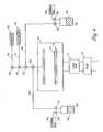
- a semiconductor wafer fragment 10includes a capacitor construction 25 formed by a method of the present invention.
- Wafer fragment 10includes a substrate 12 having a conductive diffusion area 14 formed therein.
- Substrate 12can include, for example, monocrystalline silicon.
- An insulating layer 16typically borophosphosilicate glass (BPSG), is provided over substrate 12 , with a contact opening 18 provided therein to diffusion area 14 .
- a conductive material 20fills contact opening 18 , with material 20 and oxide layer 18 having been planarized as shown.
- Material 20might be any suitable conductive material, such as, for example, tungsten or conductively doped polysilicon.
- Capacitor construction 25is provided atop layer 16 and plug 20 , and electrically connected to node 14 through plug 20 .
- Capacitor construction 25includes a first capacitor electrode 26 , which has been provided and patterned over node 20 .
- Exemplary materialsinclude conductively doped polysilicon, Pt, Ir, Rh, Ru, RuO 2 , IrO 2 , RhO 2 .
- a capacitor dielectric layer 28is provided over first capacitor electrode 26 .
- the materials of the present inventioncan be used to form the capacitor dielectric layer 28 .
- first capacitor electrode 26includes polysilicon
- a surface of the polysiliconis cleaned by an in situ HF dip prior to deposition of the dielectric material.
- An exemplary thickness for layer 28 in accordance with 256 Mb integrationis 100 Angstroms.
- a diffusion barrier layer 30is provided over dielectric layer 28 .
- Diffusion barrier layer 30includes conductive materials such as TiN, TaN, metal silicide, or metal silicide-nitride, and can be provided by CVD, for example, using conditions well known to those of skill in the art.
- a second capacitor electrode 32is formed over barrier layer 30 to complete construction of capacitor 25 .
- Second capacitor electrode 32can include constructions similar to those discussed above regarding the first capacitor electrode 26 , and can accordingly include, for example, conductively doped polysilicon.
- Diffusion barrier layer 30preferably prevents components (e.g., oxygen) from diffusing from dielectric material 28 into electrode 32 .
- Diffusion barrier layer 30can also prevent diffusion of silicon from metal electrode 32 to dielectric layer 28 .
- FIG. 2illustrates an alternative embodiment of a capacitor construction. Like numerals from FIG. 1 have been utilized where appropriate, with differences indicated by the suffix “a”.
- Wafer fragment 10 aincludes a capacitor construction 25 a differing from the construction 25 of FIG. 2 in provision of a barrier layer 30 a between first electrode 26 and dielectric layer 28 , rather than between dielectric layer 28 and second capacitor electrode 32 .
- Barrier layer 30 acan include constructions identical to those discussed above with reference to FIG. 1 .
- FIG. 3illustrates yet another alternative embodiment of a capacitor construction. Like numerals from FIG. 1 are utilized where appropriate, with differences being indicated by the suffix “b” or by different numerals.
- Wafer fragment 10 bincludes a capacitor construction 25 b having the first and second capacitor plate 26 and 32 , respectively, of the first described embodiment. However, wafer fragment 10 b differs from wafer fragment 10 of FIG. 2 in that wafer fragment 10 b includes a second barrier layer 40 in addition to the barrier layer 30 . Barrier layer 40 is provided between first capacitor electrode 26 and dielectric layer 28 , whereas barrier layer 30 is between second capacitor electrode 32 and dielectric layer 28 . Barrier layer 40 can be formed by methods identical to those discussed above with reference to FIG. 1 for formation of the barrier layer 30 .
- the barrier layersare shown and described as being distinct layers separate from the capacitor electrodes. It is to be understood, however, that the barrier layers can include conductive materials and can accordingly, in such embodiments, be understood to include at least a portion of the capacitor electrodes. In particular embodiments an entirety of a capacitor electrode can include conductive barrier layer materials.
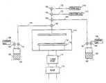
- FIG. 4A system that can be used to perform vapor deposition processes (chemical vapor deposition or atomic layer deposition) of the present invention is shown in FIG. 4 .
- the systemincludes an enclosed vapor deposition chamber 110 , in which a vacuum may be created using turbo pump 112 and backing pump 114 .
- One or more substrates 116e.g., semiconductor substrates or substrate assemblies
- a constant nominal temperatureis established for substrate 116 , which can vary depending on the process used.
- Substrate 116may be heated, for example, by an electrical resistance heater 118 on which substrate 116 is mounted. Other known methods of heating the substrate may also be utilized.
- precursor compounds 160e.g., a refractory metal precursor compound and an ether
- precursor compounds 160are stored in vessels 162 .
- the precursor compoundsare vaporized and separately fed along lines 164 and 166 to the deposition chamber 110 using, for example, an inert carrier gas 168 .
- a reaction gas 170may be supplied along line 172 as needed.
- a purge gas 174which is often the same as the inert carrier gas 168 , may be supplied along line 176 as needed.
- a series of valves 180 - 185are opened and closed as required.
- precursor compounds hafnium dimethylamide, Hf(N(CH 3 ) 2 ) 4 (Strem Chemicals, Newbury Port, Mass.), and an ozone/oxygen (O 3 /O 2 ) mixture, having approximately 10% ozone by weight,were alternately pulsed for 600 cycles into a deposition chamber containing a BPSG substrate.
- a 590 ⁇ layer of HfO 2was deposited, containing 37 atom % Hf, and 63 atom % oxygen.
- the layer of HfO 2was, surprisingly, free of carbon and nitrogen within detection limits of XPS at a substrate temperature of approximately 220° C.
Landscapes
- Chemical & Material Sciences (AREA)
- Engineering & Computer Science (AREA)
- General Chemical & Material Sciences (AREA)
- Chemical Kinetics & Catalysis (AREA)
- Materials Engineering (AREA)
- Mechanical Engineering (AREA)
- Metallurgy (AREA)
- Organic Chemistry (AREA)
- Inorganic Chemistry (AREA)
- Physics & Mathematics (AREA)
- General Physics & Mathematics (AREA)
- Manufacturing & Machinery (AREA)
- Computer Hardware Design (AREA)
- Microelectronics & Electronic Packaging (AREA)
- Power Engineering (AREA)
- Condensed Matter Physics & Semiconductors (AREA)
- Chemical Vapour Deposition (AREA)
- Formation Of Insulating Films (AREA)
Abstract
Description
- This invention relates to methods of forming a layer on a substrate using one or more metal precursor compounds and ozone during a vapor deposition process. The precursor compounds and methods are particularly suitable for the formation of a metal oxide layer, particularly a metal oxide dielectric layer, onto a semiconductor substrate or substrate assembly.
- Capacitors are the basic energy storage devices in random access memory devices, such as dynamic random access memory (DRAM) devices and static random access memory (SRAM) devices. They consist of two conductors, such as parallel metal or polysilicon plates, which act as the electrodes (i.e., the storage node electrode and the cell plate capacitor electrode), insulated from each other by a dielectric material.
- The continuous shrinkage of microelectronic devices such as capacitors and gates over the years has led to a situation where the materials traditionally used in integrated circuit technology are approaching their performance limits. Silicon (i.e., doped polysilicon) has generally been the substrate of choice, and silicon dioxide (SiO2) has frequently been used as the dielectric material with silicon to construct microelectronic devices. However, when the SiO2layer is thinned to 1 nm (i.e., a thickness of only 4 or 5 molecules), as is desired in the newest micro devices, the layer no longer effectively performs as an insulator due to the tunneling current running through it.
- Thus, new high dielectric constant materials are needed to extend device performance. Such materials need to demonstrate high permittivity, barrier height to prevent tunneling, stability in direct contact with silicon, and good interface quality and film morphology. Furthermore, such materials must be compatible with the gate material, semiconductor processing temperatures, and operating conditions.
- High quality dielectric materials based on ZrO2and HfO2, besides others, have high dielectric constants, so are being investigated as replacements in memories for SiO2where very thin layers are required. These high crystalline multivalent metal oxide layers are thermodynamically stable in the presence of silicon, minimizing silicon oxidation upon thermal annealing, and appear to be compatible with metal gate electrodes.
- This discovery has led to an effort to investigate various deposition processes to form layers, especially dielectric layers, based on zirconium and hafnium oxides and silicates. Such deposition processes have included vapor deposition, metal thermal oxidation, and high vacuum sputtering. Vapor deposition processes, which includes chemical vapor deposition (CVD) and atomic layer deposition (ALD), are very appealing as they provide for excellent control of dielectric uniformity and thickness on a substrate.
- Ritala et al., “Atomic Layer Deposition of Oxide Thin Films with Metal Alkoxides as Oxygen Sources,” SCIENCE, 288:319-321 (2000) describe a chemical approach to ALD of thin oxide films. In this approach, a metal alkoxide, serving as both a metal source and an oxygen source, reacts with another metal compound such as a metal chloride or metal alkyl to deposit a metal oxide on silicon without creating an interfacial silicon oxide layer. However, undesirable chlorine residues can also be formed. Furthermore, zirconium and hafnium alkyls are generally unstable and not commercially available. They would also likely leave carbon in the resultant films.
- Despite these continual improvements in semiconductor dielectric layers, there remains a need for a vapor deposition process utilizing sufficiently volatile metal precursor compounds that can form a thin, high quality metal oxide layer, particularly on a semiconductor substrate using a vapor deposition process.
- This invention provides, besides other things, methods of vapor depositing a metal oxide layer on a substrate. These vapor deposition methods involve forming the layer by combining one or more metal organo-amine precursor compounds with ozone. The invention also provides, besides other things, methods of depositing a silicon oxide layer on a substrate using an atomic layer deposition (ALD) process with one or more silicon organo-amine precursor compounds and ozone.
- Significantly, the methods of the present invention do not require the use of water or other hydrogen-producing coreactants, thus reducing (and typically avoiding) the problem of producing a hydrogen-containing layer.
- The methods of the present invention include forming a metal oxide layer on a substrate, as occurs in a method of manufacturing a semiconductor structure.
- In certain embodiments, a method of the present invention includes: providing a substrate (preferably a semiconductor substrate or substrate assembly such as a silicon wafer); providing at least one precursor compound of the formula M(NR1R2)x(NR3)y, wherein M is a metal, R1, R2, and R3are each independently hydrogen or an organic group, x is 1 or more, y is 0 or more, and the values of x and y are dependent on the oxidation state of M; providing at least one source of ozone; and contacting the at least one precursor compound and the at least one source of ozone to form a metal oxide layer (preferably a dielectric layer) on one or more surfaces of the substrate using a vapor deposition process.
- In another embodiment, a method of the present invention involves: providing a substrate (preferably a semiconductor substrate or substrate assembly such as a silicon wafer) within a deposition chamber; providing a vapor that includes at least one precursor compound of the formula M(NR1R2)x(NR3)y, wherein M is a metal, R1, R2, and R3are each independently hydrogen or an organic group, x is 1 or more, y is 0 or more, and the values of x and y are dependent on the oxidation state of M; providing a vapor that includes at least one source of ozone; and contacting the at least one precursor compound and the at least one source of ozone to form a metal oxide layer (preferably a dielectric layer) on one or more surfaces of the substrate using a vapor deposition process.
- In another embodiment, the present invention also provides a method of manufacturing a memory device structure, wherein the method includes: providing a substrate having a first electrode thereon; providing at least one precursor compound of the formula M(NR1R2)x(NR3)y, wherein M is a metal, R1, R2, and R3are each independently hydrogen or an organic group, x is 1 or more, y is 0 or more, and the values of x and y are dependent on the oxidation state of M; providing at least one source of ozone; vaporizing the precursor compound to form a vaporized precursor compound; directing the vaporized precursor compound and the ozone to the substrate to form a metal oxide dielectric layer on the first electrode of the substrate; and forming a second electrode on the dielectric layer. Preferably, the dielectric forms a capacitor layer, although a gate is also possible.
- In an additional embodiment, the method includes providing at least one precursor compound of the formula M(NR1R2)x(NR3)y, wherein y is 0 to 4, and x is 1 to 8. Preferably, y is 0, thereby providing at least one precursor compound of the formula M(NR1R2)x, wherein a value of x is dependent on the oxidation state of M. Preferably the compound of formula M(NR1R2)x(NR3)yexcludes silicon as M when the vapor deposition process is a chemical vapor deposition process.
- In another embodiment, a method of the present invention includes forming a silicon oxide layer (typically silicon dioxide) on a substrate. One such method includes: providing a substrate (preferably a semiconductor substrate or substrate assembly such as a silicon wafer); providing at least one precursor compound of the formula Si(NR1R2)xZy, wherein R1and R2are each independently hydrogen or an organic group, Z is Cl or H, x is 1 to 4, y is 0 to 4; providing at least one source of ozone; and contacting the at least one precursor compound and the at least one source of ozone to form a silicon oxide layer (preferably an SiO2insulating layer) on one or more surfaces of the substrate using an atomic layer deposition process that includes a plurality of deposition cycles.
- In an additional embodiment, a method of the present invention includes forming a silicon oxide layer on a substrate by providing a substrate (preferably a semiconductor substrate or substrate assembly such as a silicon wafer) within a deposition chamber; providing at least one precursor compound of the formula Si(NR1R2)xZy, wherein R1and R2are each independently hydrogen or an organic group, Z is Cl or H, x is 1 to 4, y is 0 to 4; providing at least one source of ozone; and contacting the at least one precursor compound and the at least one source of ozone to form a silicon oxide layer (preferably an SiO2insulating layer) on one or more surfaces of the substrate within the deposition chamber using an atomic layer deposition process that includes a plurality of deposition cycles.
- Another method of the present invention includes a method of manufacturing a memory device structure with an atomic layer deposition process, the method includes providing a substrate having a first electrode thereon; providing at least one precursor compound of the formula Si(NR1R2)xZy, wherein R1and R2are each independently hydrogen or an organic group, Z is Cl or H, x is 1 to 4, and y is 0 to 4; providing at least one source of ozone; vaporizing the precursor compound to form a vaporized precursor compound; directing the vaporized precursor compound and the ozone to the substrate to form a silicon oxide dielectric layer on the first electrode of the substrate with the atomic layer deposition process; and forming a second electrode on the dielectric layer.
- The methods of the present invention can utilize a chemical vapor deposition (CVD) process, which can be pulsed, or an atomic layer deposition (ALD) process (a self-limiting vapor deposition process that includes a plurality of deposition cycles, typically with purging between the cycles). Preferably, the methods of the present invention use ALD. For certain ALD processes, the precursor compounds can be alternately introduced into a deposition chamber during each deposition cycle.
- The present invention also provides a vapor deposition apparatus that includes: a vapor deposition chamber having a substrate positioned therein; one or more vessels that include at least one precursor compound of the formula M(NR1R2)x(NR3)y, wherein M is a metal except silicon, R1, R2, and R3are each independently a hydrogen or an organic group, x is 1 or more, y is 0 or more, and the values of x and y are dependent on the oxidation state of M; and one or more sources of ozone, such as an ozone generator that delivers an ozone oxygen mixture.
- The present invention further includes an atomic layer vapor deposition apparatus that includes: a deposition chamber having a substrate (preferably a semiconductor substrate or substrate assembly such as a silicon wafer) positioned therein; one or more vessels that include at least one precursor compound of the formula Si(NR1R2)xZy, wherein R1and R2are each independently hydrogen or an organic group, Z is Cl or H, x is 1 to 4, and y is 0 to 4; and one or more sources of ozone such as an ozone generator that delivers an ozone oxygen mixture.
- For certain embodiments, the metal oxide layer can include an alloy, a solid solution, or a nanolaminate. For certain embodiments, the metal oxide layer can include a solid solution that includes, for example, a zirconium oxide, an aluminum oxide, a tantalum oxide, a titanium oxide, a niobium oxide, a hafnium oxide, an oxide of a lanthanide, or combinations thereof.
- In an additionally preferred embodiment, a solid solution of the metal oxide layer can also include a silicon oxide (including silicates) when a silicon-containing precursor compound is provided. Thus, a solid solution can have any combination of metal oxide layer, including a silicon oxide, if desired.
- In addition, preferably the metal oxide layer is essentially free of carbon, nitrogen, and halogens, or compounds thereof. As used herein, “essentially free” is defined to mean that the metal oxide layer has less than about 1% by weight of carbon, nitrogen, hydrogen, halogens, or compounds thereof such that the presence of these elements and/or compounds thereof having a minor effect on the chemical, mechanical, or electrical properties of the film.
- “Semiconductor substrate” or “substrate assembly” as used herein refers to a semiconductor substrate such as a base semiconductor layer or a semiconductor substrate having one or more layers, structures, or regions formed thereon. A base semiconductor layer is typically the lowest layer of silicon material on a wafer or a silicon layer deposited on another material, such as silicon on sapphire. When reference is made to a substrate assembly, various process steps may have been previously used to form or define regions, junctions, various structures or features, and openings such as capacitor plates or barriers for capacitors.
- “Layer” as used herein refers to any layer that can be formed on a substrate from the precursor compounds of this invention using a vapor deposition process. The term “layer” is meant to include layers specific to the semiconductor industry, such as “barrier layer,” “dielectric layer,” “insulating layer,” and “conductive layer.” (The term “layer” is synonymous with the term “film” frequently used in the semiconductor industry.) The term “layer” is also meant to include layers found in technology outside of semiconductor technology, such as coatings on glass.
- “Dielectric layer” as used herein refers to a layer (or film) having a high dielectric constant containing primarily, for example, zirconium oxides, aluminum oxides, tantalum oxides, titanium oxides, niobium oxides, hafnium oxides, an oxide of a lanthanide, or combinations thereof.
- “Precursor compound” as used herein refers to an organo-amine (such as diorganoamide (e.g., dialkylamide) or alkylimines-alkylamines) precursor compound, for example, capable of forming a metal oxide layer on a substrate with ozone in a vapor deposition process or a silicon dioxide layer on a substrate with ozone in an atomic layer deposition process. The organo-amine precursor compounds are all preferably liquid at the vaporization temperature, and more preferably at room temperature. In one example, the precursor compounds are organometallic compounds that form volatile by-products upon reacting.
- “Deposition process” and “vapor deposition process” as used herein refer to a process in which a layer is formed on one or more surfaces of a substrate (e.g., a doped polysilicon wafer) from vaporized precursor compound(s). Specifically, one or more precursor compounds are vaporized and directed to one or more surfaces of a heated substrate (e.g., semiconductor substrate or substrate assembly) placed in a deposition chamber. These precursor compounds form (e.g., by reacting or decomposing) a non-volatile, thin, uniform, layer on the surface(s) of the substrate. For the purposes of this invention, the term “vapor deposition process” is meant to include both chemical vapor deposition processes (including pulsed chemical vapor deposition processes) and atomic layer deposition processes.
- “Chemical vapor deposition” (CVD) as used herein refers to a vapor deposition process wherein the desired layer is deposited on the substrate from vaporized metal precursor compounds (and any reaction gases used) within a deposition chamber with no effort made to separate the reaction components. In contrast to a “simple” CVD process that involves the substantial simultaneous use of the precursor compounds and any reaction gases, “pulsed” CVD alternately pulses these materials into the deposition chamber, but does not rigorously avoid intermixing of the precursor and reaction gas streams, as is typically done in atomic layer deposition or ALD (discussed in greater detail below).
- “Atomic layer deposition” (ALD) as used herein refers to a vapor deposition process in which numerous consecutive deposition cycles are conducted in a deposition chamber. Typically, during each cycle the precursor compound is chemisorbed to the substrate surface; excess precursor is purged out; a subsequent precursor and/or reaction gas is introduced to react with the chemisorbed layer; and excess reaction gas (if used) and by-products are removed. As compared to the one cycle chemical vapor deposition (CVD) process, the longer duration multi-cycle ALD process allows for improved control of layer thickness by self-limiting layer growth and minimizing detrimental gas phase reactions by separation of the reaction components. The term “atomic layer deposition” as used herein is also meant to include the related terms “atomic layer epitaxy” (ALE), molecular beam epitaxy (MBE), gas source MBE, organometallic MBE, and chemical beam epitaxy when performed with alternating pulses of precursor compound(s), reaction gas(es), and purge (i.e., inert carrier) gas.
- “Chemisorption” as used herein refers to the chemical adsorption of vaporized reactive precursor compounds on the surface of a substrate. The adsorbed species are irreversibly bound to the substrate surface as a result of relatively strong binding forces characterized by high adsorption energies (e.g., >30 kcal/mol), comparable in strength to ordinary chemical bonds. The chemisorbed species typically form a monolayer on the substrate surface. (See “The Condensed Chemical Dictionary”, 10th edition, revised by G. G. Hawley, published by Van Nostrand Reinhold Co., New York, 225 (1981)). The technique of ALD is based on the principle of the formation of a saturated monolayer of reactive precursor molecules by chemisorption. In ALD one or more appropriate precursor compounds or reaction gases are alternately introduced (e.g., pulsed) into a deposition chamber and chemisorbed onto the surfaces of a substrate. Each sequential introduction of a reactive compound (e.g., one or more precursor compounds and one or more reaction gases) is typically separated by an inert carrier gas purge. Each precursor compound co-reaction adds a new atomic layer to previously deposited layers to form a cumulative solid layer. The cycle is repeated to gradually form the desired layer thickness. It should be understood that ALD can alternately utilize one precursor compound, which is chemisorbed, and one reaction gas, which reacts with the chemisorbed species.
FIGS. 1-3 are exemplary capacitor constructions.FIG. 4 is a perspective view of a vapor deposition coating system suitable for use in the method of the present invention.- The present invention provides, besides other things, methods of forming a metal oxide layer (preferably a metal oxide dielectric layer) on a substrate (preferably a semiconductor substrate or substrate assembly) using one or more metal organo-amine precursor compounds with an ozone source. The invention also provides, besides other things, methods of depositing a silicon oxide layer (typically a silicon dioxide layer) on a substrate using an atomic layer deposition (ALD) process. Preferably, the ALD process involves forming the silicon oxide layer by combining one or more silicon organo-amine precursor compounds with ozone.
- Preferably, the organo-amine precursor compounds include precursor compounds having the formula M(NR1R2)x(NR3)y(Formula I), wherein M is a metal, R1, R2, and R3are each independently a hydrogen or an organic group, x is 1 or more, y is 0 or more, and the values of x and y are dependent on the oxidation state of M. In an additional preferred embodiment, the method includes providing at least one precursor compound of the formula M(NR1R2)x(NR3)y, wherein y is 0 to 4 and x is 1 to 8. Preferably, y is 0, thereby providing at least one precursor compound of the formula M(NR1R2)x(Formula II), wherein a value of x is dependent on the oxidation state of M.
- In Formulas I and II: M can be any metal (main group, transition metal, lanthanide, or metalloid (thereby including B, Al, Ge, Si, As, Sb, Te, Po, and At) although silicon is excluded for certain embodiments, particularly when used in a chemical vapor deposition process; each R (i.e., R1, R2, and R3) is independently a hydrogen or an organic group; preferably, x is 1 to 8, more preferably, x is 2 to 6; preferably, y is 0 to 4, more preferably y is 0 to 2. Preferably, in Formula II, the value of x is 4 or 5 and the value of y is 0.
- The metal oxide layer formed according to the present invention may include one or more different metals and is typically of the formula MnOm(Formula III), wherein M can be one or more of the metals as defined above (i.e., the oxide can be a single metal oxide or a mixed metal oxide). Preferably, the metal oxide layer is a single metal oxide (i.e., includes only one metal). It is possible, however, for the metal oxide layer to include two or more different metals.
- If the metal oxide layer includes two or more different metals, the metal oxide layer can be in the form of alloys, solid solutions, or nanolaminates. Preferably, these have dielectric properties. The metal oxide layer (particularly if it is a dielectric layer) preferably includes one or more of ZrO2, HfO2, Ta2O3, Al2O3, Nb2O5, Ta2O5, TiO2, and an oxide of a lanthanide.
- Surprisingly, the metal oxide layer formed according to the present invention is essentially free of carbon, nitrogen, hydrogen, and halogens, or compounds thereof. As used herein, “essentially free” is defined to mean that the metal oxide layer has less than about 1% by weight of carbon, nitrogen, hydrogen, halogens, or compounds thereof such that the presence of these elements and/or compounds thereof have minor effect on the chemical, mechanical, or electrical properties of the film.
- The substrate on which the metal oxide layer is formed is preferably a semiconductor substrate or substrate assembly. Any suitable semiconductor material is contemplated, such as for example, conductively doped polysilicon (for this invention simply referred to as “silicon”). A substrate assembly may also contain a layer that includes platinum, iridium, rhodium, ruthenium, ruthenium oxide, titanium nitride, tantalum nitride, tantalum-silicon-nitride, silicon dioxide, silicon nitride, aluminum, gallium arsenide, glass, etc., and other existing or to-be-developed materials used in semiconductor constructions, such as dynamic random access memory (DRAM) devices and static random access memory (SRAM) devices, for example.
- Substrates other than semiconductor substrates or substrate assemblies can be used in methods of the present invention. These include, for example, fibers, wires, etc. If the substrate is a semiconductor substrate or substrate assembly, the layers can be formed directly on the lowest semiconductor surface of the substrate, or they can be formed on any of a variety of the layers (i.e., surfaces) as in a patterned wafer, for example.
- The precursor compounds described herein may include a wide variety of metals. As used herein, “metal” includes all metals of the periodic table (including main group metals, transition metals, lanthanides, actinides, and metalloid such as B, Al, Ge, Si, As, Sb, Te, Po, and At but excluding Si for certain embodiments). For certain methods of the present invention, preferably, each metal M is selected from the group of metals of Group 3 (Sc, Y), Group 4 (Ti, Zr, Hf), 5 (V, Nb, Ta), Group 13 (Al, Ga, In), the lanthanides (La, Ce, Pr, etc.) of the Periodic Chart, and combinations thereof. Preferably, M is selected from the group consisting of Al, Ti, Zr, Hf, Nb, Ta, a lanthanide (e.g., La, Ce, Pr, Nd, Pm, Sm, Eu, Gd, Tb, Dy, Ho, Er, Tm, Yb, and Lu), and combinations thereof. More preferably, M is selected from the group consisting of Ti, Hf, Nb, Ta, Al, Zr, and combinations thereof.
- In Formula I: M is a metal selected from Group 3 (Sc, Y), Group 4 (Ti, Zr, Hf), Group 5 (V, Nb, Ta), Group 13 (Al, Ga, In), the lanthanides of the Periodic Table, and combinations thereof. Preferred and more preferred metals for Formula I are as defined above.
- In Formula II: M is a metal selected from Groups 3 (Sc, Y), 4 (Ti, Zr, Hf), 5 (V, Nb, Ta), the lanthanides of the Periodic Table, and combinations thereof. Preferably, M is selected from the group consisting of Ti, Zr, Hf, Nb, Ta, a lanthanide (e.g., La, Ce, Pr, Nd, Pm, Sm, Eu, Gd, Tb, Dy, Ho, Er, Tm, Yb, and Lu), and combinations thereof. For certain methods of the present invention, preferably, M is selected from the group consisting of Ti, Zr, Hf, Nb, Ta, and combinations thereof.
- Preferably, the precursor compounds useful in this invention are of the formula M(NR1R2)x(NR3)y(Formula I), wherein M is a metal, R1, R2and R3are each independently a hydrogen or an organic group (as described in greater detail below), and x is 1 to 8 and y is 0 to 4, depending on the oxidation state of M. In an additional preferred embodiment, the precursor compounds useful in this invention are of the formula M(NR1R2)x(Formula II), wherein M is a metal, R1and R2are each independently a hydrogen or an organic group (as described in greater detail below), and the value of x is dependent on the oxidation state of M, and preferably x is 4 or 5 depending on the oxidation state of M.
- For ALD processes, the metal M of the compounds of Formula I and II can further include all metals of the Periodic Table (including main group metals, transition metals, lanthanides, actinides, and metalloids including Si).
- For the CVD or ALD processes, organo-amine precursor compounds include precursor compounds having the formula Si(NR1R2)xZy(Formula III), wherein R1and R2are each independently hydrogen or an organic group, Z is Cl or H, x is 1 to 4, and y is 0 to 4; and precursor compounds having the formula Si(NR1R2)x(Formula IV), wherein R1and R2are each independently an organic group, x is 4.
- As used herein, the term “organic group” is used for the purpose of this invention to mean a hydrocarbon group that is classified as an aliphatic group, cyclic group, or combination of aliphatic and cyclic groups (e.g., alkaryl and aralkyl groups). In the context of the present invention, suitable organic groups for precursor compounds of this invention are those that do not interfere with the formation of a metal oxide layer using vapor deposition techniques. In the context of the present invention, the term “aliphatic group” means a saturated or unsaturated linear or branched hydrocarbon group. This term is used to encompass alkyl, alkenyl, and alkynyl groups, for example. The term “alkyl group” means a saturated linear or branched monovalent hydrocarbon group including, for example, methyl, ethyl, n-propyl, isopropyl, t-butyl, amyl, heptyl, and the like. The term “alkenyl group” means an unsaturated, linear or branched monovalent hydrocarbon group with one or more olefinically unsaturated groups (i.e., carbon-carbon double bonds), such as a vinyl group. The term “alkynyl group” means an unsaturated, linear or branched monovalent hydrocarbon group with one or more carbon-carbon triple bonds. The term “cyclic group” means a closed ring hydrocarbon group that is classified as an alicyclic group, aromatic group, or heterocyclic group. The term “alicyclic group” means a cyclic hydrocarbon group having properties resembling those of aliphatic groups. The term “aromatic group” or “aryl group” means a mono- or polynuclear aromatic hydrocarbon group. The term “heterocyclic group” means a closed ring hydrocarbon in which one or more of the atoms in the ring is an element other than carbon (e.g., nitrogen, oxygen, sulfur, etc.).
- As a means of simplifying the discussion and the recitation of certain terminology used throughout this application, the terms “group” and “moiety” are used to differentiate between chemical species that allow for substitution or that may be substituted and those that do not so allow for substitution or may not be so substituted. Thus, when the term “group” is used to describe a chemical substituent, the described chemical material includes the unsubstituted group and that group with nonperoxidic O, N, Si, F, or S atoms, for example, in the chain as well as carbonyl groups or other conventional substituents. Where the term “moiety” is used to describe a chemical compound or substituent, only an unsubstituted chemical material is intended to be included. For example, the phrase “alkyl group” is intended to include not only pure open chain saturated hydrocarbon alkyl substituents, such as methyl, ethyl, propyl, t-butyl, and the like, but also alkyl substituents bearing further substituents known in the art, such as hydroxy, alkoxy, alkylsulfonyl, halogen atoms, cyano, nitro, amino, carboxyl, etc. Thus, “alkyl group” includes ether groups, haloalkyls, nitroalkyls, carboxyalkyls, hydroxyalkyls, sulfoalkyls, etc. On the other hand, the phrase “alkyl moiety” is limited to the inclusion of only pure open chain saturated hydrocarbon alkyl substituents, such as methyl, ethyl, propyl, t-butyl, and the like.
- For all the precursor compounds of this invention, each R (i.e., R1, R2, and R3) is independently and preferably hydrogen or an organic group, more preferably a (C1-C10) organic group, even more preferably a (C1-C8) organic group, even more preferably a (C1-C6) organic group, and even more preferably a “lower” (i.e., C1-C4) organic group. Even more preferably, each of these organic groups is an alkyl group. Most preferably, each organic group is an organic moiety, and preferably, an alkyl moiety (particularly methyl and ethyl moieties).
- In certain embodiments, the carbon atoms of the R groups are optionally replaced by or substituted with silicon (e.g., R═SiMe3of SiHMe2), fluorine (e.g., fluorocarbyl groups), oxygen, and/or nitrogen atoms or groups containing such atoms. So, the R groups can each independently be organic groups containing silicon substituted for one or more of the carbon atoms. Thus, silylated imine-amines and silylated amines are within the scope of Formulas I and II, respectively. Also, such heteroatoms may bond to the metal, thereby forming multidentate ligands.
- For the compounds of Formula I, M(NR1R2)x(NR3)y, each R is preferably a (C1-C6) organic group. Examples of suitable precursor compounds include Al(NMe2)2(N(Me)CH2CH2NMe2) and Ta(N—tBu)(NEt2)3, which are either commercially available from sources such as Strem Chemical Co., or they can be prepared using standard techniques (e.g., by reacting metal chlorides with the corresponding lithium dialkyl amides).
- For the compounds of Formula II, M(NR1R2)x, each R is preferably a (C1-C6) organic group.
- For hafnium precursor compounds of the formula Hf(NR1R2)4, R1and R2are preferably both methyl, both ethyl, or one each of methyl and ethyl. Examples of suitable hafnium precursor compounds include tetrakis(dimethylamino) hafnium and tetrakis(ethylmethylamino) hafnium, the latter available from Sigma-Aldrich Chemical Co.
- For zirconium precursor compounds of the formula Zr(NR1R2)4, R1and R2are preferably both methyl, both ethyl, or one each of methyl and ethyl. Examples of suitable zirconium precursor compounds include tetrakis(dimethylamino) zirconium, tetrakis(diethylamino) zirconium and tetrakis(ethylmethylamino) zirconium, all available from Sigma-Aldrich Chemical Co.
- For the titanium precursor compounds of the formula Ti(NR1R2)4, R1and R2are preferably both methyl, both ethyl, or one each of methyl and ethyl. Examples of suitable titanium precursor compounds include tetrakis(dimethylamino) titanium, tetrakis(diethylamino) titanium, and tetrakis(ethylmethylamino) titanium, all available from Sigma-Aldrich Chemical Co.
- For the niobium precursor compounds of the formula Nb(NR1R2)5, R1and R2are preferably both methyl, both ethyl, or one each of methyl and ethyl. Examples of suitable niobium precursor compounds include pentakis(ethylmethylamino) niobium available from ATMI (Danbury, Conn.).
- For the tantalum precursor compounds of the formula Ta(NR1R2)3(NR3), R1and R2are preferably both methyl, both ethyl, or one each of methyl and ethyl, and R3is tert-butyl. Examples of suitable tantalum precursor compounds include Ta(N—tBu)(NEt2)3available from InorgTech (Mildenhall, Suffolk, UK).
- Various precursor compounds can be used in various combinations, optionally with one or more organic solvents (particularly for CVD processes), to form a precursor composition. The precursor compounds may be liquids or solids at room temperature (preferably, they are liquids at the vaporization temperature). Typically, they are liquids sufficiently volatile to be employed using known vapor deposition techniques. However, as solids they may also be sufficiently volatile that they can be vaporized or sublimed from the solid state using known vapor deposition techniques.
- The precursor compounds can be vaporized in the presence of an inert carrier gas if desired. Additionally, an inert carrier gas can be used in purging steps in an ALD process. The inert carrier gas is typically selected from the group consisting of nitrogen, helium, argon, and combinations thereof. In the context of the present invention, an inert carrier gas is one that does not interfere with the formation of the oxide layers of the present invention.
- The deposition process for this invention is a vapor deposition process. Vapor deposition processes are generally favored in the semiconductor industry due to the process capability to quickly provide highly conformal layers even within deep contacts and other openings. Chemical vapor deposition (CVD) and atomic layer deposition (ALD) are two vapor deposition processes often employed to form thin, continuous, uniform, metal oxide (preferably dielectric) layers onto semiconductor substrates. Using either vapor deposition process, typically one or more precursor compounds are vaporized in a deposition chamber and optionally combined with one or more reaction gases to form a metal oxide layer onto a substrate. It will be readily apparent to one skilled in the art that the vapor deposition process may be enhanced by employing various related techniques such as plasma assistance, photo assistance, laser assistance, as well as other techniques.
- The final layer formed preferably has a thickness in the range of about 10 Å to about 500 Å. Preferably, the thickness of the metal oxide layer is in the range of about 30 Å to about 100 Å.
- For certain embodiments, the layer formed using the methods of the present invention are dielectric layers. For certain other embodiments, insulating layers are formed, particularly when silicon dioxide is formed.
- For certain embodiments, the metal oxide layer can include an alloy, a solid solution, or a nanolaminate. For certain embodiments, the metal oxide layer can include a solid solution that includes, for example, a zirconium oxide, an aluminum oxide, a tantalum oxide, a titanium oxide, a niobium oxide, a hafnium oxide, an oxide of a lanthanide, or combinations thereof.
- In an additionally preferred embodiment, a solid solution of the metal oxide layer can also include a silicon oxide (including silicates) when a silicon-containing precursor compound is provided. Thus, a solid solution can have any combination of metal oxide layer, including a silicon oxide, if desired.
- Chemical vapor deposition (CVD) has been extensively used for the preparation of metal oxide layers, such as dielectric layers, in semiconductor processing because of its ability to provide highly conformal and high quality dielectric layers at relatively fast processing times. The desired precursor compounds are vaporized and then introduced into a deposition chamber containing a heated substrate with reaction gases and/or inert carrier gases. In a typical CVD process, vaporized precursors are contacted with reaction gas(es) at the substrate surface to form a layer (e.g., dielectric layer). The single deposition cycle is allowed to continue until the desired thickness of the layer is achieved.
- Typical CVD processes generally employ precursor compounds in vaporization chambers that are separated from the process chamber wherein the deposition surface or wafer is located. For example, liquid precursor compounds are typically placed in bubblers and heated to a temperature at which they vaporize, and the vaporized liquid precursor compound is then transported by an inert carrier gas passing over the bubbler or through the liquid precursor compound. The vapors are then swept through a gas line to the deposition chamber for depositing a layer on substrate surface(s) therein. Many techniques have been developed to precisely control this process. For example, the amount of precursor material transported to the deposition chamber can be precisely controlled by the temperature of the reservoir containing the precursor compound and by the flow of an inert carrier gas bubbled through or passed over the reservoir.
- Preferred embodiments of the metal oxide precursor compounds described herein are particularly suitable for chemical vapor deposition (CVD). The deposition temperature at the substrate surface is preferably held at a temperature in a range of about 100° C. to about 600° C., more preferably in the range of about 200° C. to about 500° C. The deposition chamber pressure is preferably maintained at a deposition pressure of about 0.1 torr to about 10 torr. The partial pressure of precursor compounds in the inert carrier gas is preferably about 0.001 torr to about 10 torr.
- Several modifications of the CVD process and chambers are possible, for example, using atmospheric pressure chemical vapor deposition, low pressure chemical vapor deposition (LPCVD), plasma enhanced chemical vapor deposition (PECVD), hot wall or cold wall reactors or any other chemical vapor deposition technique. Furthermore, pulsed CVD can be used, which is similar to ALD (discussed in greater detail below) but does not rigorously avoid intermixing of precursor and reactant gas streams. Also, for pulsed CVD, the deposition thickness is dependent on the exposure time, as opposed to ALD, which is self-limiting (discussed in greater detail below).
- A typical CVD process may be carried out in a chemical vapor deposition reactor, such as a deposition chamber available under the trade designation of 7000 from Genus, Inc. (Sunnyvale, Calif.), a deposition chamber available under the trade designation of 5000 from Applied Materials, Inc. (Santa Clara, Calif.), or a deposition chamber available under the trade designation of Prism from Novelus, Inc. (San Jose, Calif.). However, any deposition chamber suitable for performing CVD may be used.
- Alternatively, and preferably, the vapor deposition process employed in the methods of the present invention is a multi-cycle ALD process. More preferably, the multi-cycle ALD process is used when the compounds of Formula I and II include M as Si. Such a process is advantageous (particularly over a CVD process) in that in provides for optimum control of atomic-level thickness and uniformity to the deposited layer (e.g., dielectric layer) and to expose the precursor compounds (both metal precursor compounds and silicon precursor compounds) to lower volatilization and reaction temperatures to minimize degradation. Typically, in an ALD process, each reactant is pulsed sequentially onto a suitable substrate, typically at deposition temperatures of about 25° C. to about 400° C. (preferably about 150° C. to about 300° C.), which is generally lower than presently used in CVD processes. Under such conditions the film growth is typically self-limiting (i.e., when the reactive sites on a surface are used up in an ALD process, the deposition generally stops), insuring not only excellent conformality but also good large area uniformity plus simple and accurate thickness control. Due to alternate dosing of the precursor compounds and/or reaction gases, detrimental vapor-phase reactions are inherently eliminated, in contrast to the CVD process that is carried out by continuous coreaction of the precursors and/or reaction gases. (See Vehkamäki et al, “Growth of SrTiO3and BaTiO3Thin Films by Atomic Layer Deposition,” Electrochemical and Solid-State Letters, 2(10):504-506 (1999)).
- A typical ALD process includes exposing an initial substrate to a first chemical species (e.g., a precursor compound of Formulas I-IV) to accomplish chemisorption of the species onto the substrate. Theoretically, the chemisorption forms a monolayer that is uniformly one atom or molecule thick on the entire exposed initial substrate. In other words, a saturated monolayer. Practically, chemisorption might not occur on all portions of the substrate. Nevertheless, such an imperfect monolayer is still a monolayer in the context of the present invention. In many applications, merely a substantially saturated monolayer may be suitable. A substantially saturated monolayer is one that will still yield a deposited layer exhibiting the quality and/or properties desired for such layer.
- The first species is purged from over the substrate and ozone is provided to react with the first monolayer of the first species. The ozone is then purged and a second chemical species (e.g., a different precursor compound of Formulas I-IV) is then purged form over the substrate and ozone is provided to react with the monolayer of the second species. The steps are repeated with exposure of the first species to the ozone. In some cases, the two monolayers may be of the same species. In an additional embodiment, the ozone used in the present invention may be mixed with oxygen and/or with inert gases.
- Purging may involve a variety of techniques including, but not limited to, contacting the substrate and/or monolayer with a carrier gas and/or lowering pressure to below the deposition pressure to reduce the concentration of a species contacting the substrate and/or chemisorbed species. Examples of carrier gases include N2, Ar, He, etc. Purging may instead include contacting the substrate and/or monolayer with any substance that allows chemisorption by-products to desorb and reduces the concentration of a contacting species preparatory to introducing another species. The contacting species may be reduced to some suitable concentration or partial pressure known to those skilled in the art based on the specifications for the product of a particular deposition process.
- ALD is often described as a self-limiting process, in that a finite number of sites exist on a substrate to which the first species may form chemical bonds. The second species might only bond to the first species and thus may also be self-limiting. Once all of the finite number of sites on a substrate are bonded with a first species, the first species will often not bond to other of the first species already bonded with the substrate. However, process conditions can be varied in ALD to promote such bonding and render ALD not self-limiting. Accordingly, ALD may also encompass a species forming other than one monolayer at a time by stacking of a species, forming a layer more than one atom or molecule thick.
- The described method indicates the “substantial absence” of the second precursor (i.e., second species) during chemisorption of the first precursor since insignificant amounts of the second precursor might be present. According to the knowledge and the preferences of those with ordinary skill in the art, a determination can be made as to the tolerable amount of second precursor and process conditions selected to achieve the substantial absence of the second precursor.
- Thus, during the ALD process, numerous consecutive deposition cycles are conducted in the deposition chamber, each cycle depositing a very thin metal oxide layer or a very thin silicon dioxide layer (usually less than one monolayer such that the growth rate on average is from about 0.2 to about 3.0 Angstroms per cycle), until a layer of the desired thickness is built up on the substrate of interest. The layer deposition is accomplished by alternately introducing (i.e., by pulsing) precursor compounds into the deposition chamber containing a semiconductor substrate, chemisorbing the precursor compound(s) as a monolayer onto the substrate surfaces, and then reacting the chemisorbed precursor compound(s) with ozone. The pulse duration of precursor compound(s) and inert carrier gas(es) is sufficient to saturate the substrate surface. Typically, the pulse duration is from about 0.1 to about 5 seconds, preferably from about 0.2 to about 1 second.
- In comparison to the predominantly thermally driven CVD, ALD is predominantly chemically driven. Accordingly, ALD is often conducted at much lower temperatures than CVD. During the ALD process, the substrate temperature is maintained at a temperature sufficiently low to maintain intact bonds between the chemisorbed precursor compound(s) and the underlying substrate surface and to prevent decomposition of the precursor compound(s). The temperature is also sufficiently high to avoid condensation of the precursor compounds(s). Typically the substrate temperature is kept within the range of about 25° C. to about 400° C. (preferably about 150° C. to about 300° C.), which is generally lower than presently used in CVD processes. Thus, the first species or precursor compound is chemisorbed at this temperature. Surface reaction of the precursor compound can occur at substantially the same temperature as chemisorption of the precursor or, less preferably, at a substantially different temperature. Clearly, some small variation in temperature, as judged by those of ordinary skill, can occur but still be a substantially same temperature by providing a reaction rate statistically the same as would occur at the temperature of the precursor chemisorption. Chemisorption and subsequent reactions could instead occur at exactly the same temperature.
- For a typical ALD process, the pressure inside the deposition chamber is kept at about 10−4torr to about 1 torr, preferably about 10−4torr to about 0.1 torr. Typically, the deposition chamber is purged with an inert carrier gas after the vaporized precursor compound(s) have been introduced into the chamber and/or reacted for each cycle. The inert carrier gas(es) can also be introduced with the vaporized precursor compound(s) during each cycle.
- The reactivity of a precursor compound can significantly influence the process parameters in ALD. Under typical CVD process conditions, a highly reactive compound may react in the gas phase generating particulates, depositing prematurely on undesired surfaces, producing poor films, and/or yielding poor step coverage or otherwise yielding non-uniform deposition. For at least such reason, a highly reactive compound might be considered not suitable for CVD. However, some compounds not suitable for CVD are superior ALD precursors. For example, if the first precursor is gas phase reactive with the second precursor, such a combination of compounds might not be suitable for CVD, although they could be used in ALD. In the CVD context, concern might also exist regarding sticking coefficients and surface mobility, as known to those skilled in the art, when using highly gas-phase reactive precursors, however, little or no such concern would exist in the ALD context.
- After layer formation on the substrate, an annealing process can be optionally performed in situ in the deposition chamber in a nitrogen atmosphere or oxidizing atmosphere. Preferably, the annealing temperature is within the range of about 400° C. to about 1000° C. Particularly after ALD, the annealing temperature is more preferably about 400° C. to about 750° C., and most preferably about 600° C. to about 700° C. Alternatively, the annealing process can also include annealing in a plasma. The annealing operation is preferably performed for a time period of about 0.5 minute to about 60 minutes and more preferably for a time period of about 1 minute to about 10 minutes. One skilled in the art will recognize that such temperatures and time periods may vary. For example, furnace anneals and rapid thermal annealing may be used, and further, such anneals may be performed in one or more annealing steps.
- As stated above, the use of the complexes and methods of forming films of the present invention are beneficial for a wide variety of thin film applications in semiconductor structures, particularly those using high dielectric materials. For example, such applications include capacitors such as planar cells, trench cells (e.g., double sidewall trench capacitors), stacked cells (e.g., crown, V-cell, delta cell, multi-fingered, or cylindrical container stacked capacitors), as well as field effect transistor devices. Thus, for certain embodiments, the dielectric layer forms a capacitor layer. Alternatively, the dielectric layer forms a gate.
- A specific example of where a dielectric layer is formed according to the present invention is a capacitor construction. Exemplary capacitor constructions are described with reference to
FIGS. 1-3 . Referring toFIG. 1 , asemiconductor wafer fragment 10 includes acapacitor construction 25 formed by a method of the present invention.Wafer fragment 10 includes asubstrate 12 having aconductive diffusion area 14 formed therein.Substrate 12 can include, for example, monocrystalline silicon. An insulatinglayer 16, typically borophosphosilicate glass (BPSG), is provided oversubstrate 12, with acontact opening 18 provided therein todiffusion area 14. Aconductive material 20 fillscontact opening 18, withmaterial 20 andoxide layer 18 having been planarized as shown.Material 20 might be any suitable conductive material, such as, for example, tungsten or conductively doped polysilicon.Capacitor construction 25 is provided atoplayer 16 and plug20, and electrically connected tonode 14 throughplug 20. Capacitor construction 25 includes afirst capacitor electrode 26, which has been provided and patterned overnode 20. Exemplary materials include conductively doped polysilicon, Pt, Ir, Rh, Ru, RuO2, IrO2, RhO2. Acapacitor dielectric layer 28 is provided overfirst capacitor electrode 26. The materials of the present invention can be used to form thecapacitor dielectric layer 28. Preferably, iffirst capacitor electrode 26 includes polysilicon, a surface of the polysilicon is cleaned by an in situ HF dip prior to deposition of the dielectric material. An exemplary thickness forlayer 28 in accordance with 256 Mb integration is 100 Angstroms.- A
diffusion barrier layer 30 is provided overdielectric layer 28.Diffusion barrier layer 30 includes conductive materials such as TiN, TaN, metal silicide, or metal silicide-nitride, and can be provided by CVD, for example, using conditions well known to those of skill in the art. After formation ofbarrier layer 30, asecond capacitor electrode 32 is formed overbarrier layer 30 to complete construction ofcapacitor 25.Second capacitor electrode 32 can include constructions similar to those discussed above regarding thefirst capacitor electrode 26, and can accordingly include, for example, conductively doped polysilicon.Diffusion barrier layer 30 preferably prevents components (e.g., oxygen) from diffusing fromdielectric material 28 intoelectrode 32. If, for example, oxygen diffuses into a silicon-containingelectrode 32, it can undesirably form SiO2, which will significantly reduce the capacitance ofcapacitor 25.Diffusion barrier layer 30 can also prevent diffusion of silicon frommetal electrode 32 todielectric layer 28. FIG. 2 illustrates an alternative embodiment of a capacitor construction. Like numerals fromFIG. 1 have been utilized where appropriate, with differences indicated by the suffix “a”.Wafer fragment 10aincludes acapacitor construction 25adiffering from theconstruction 25 ofFIG. 2 in provision of abarrier layer 30abetweenfirst electrode 26 anddielectric layer 28, rather than betweendielectric layer 28 andsecond capacitor electrode 32.Barrier layer 30acan include constructions identical to those discussed above with reference toFIG. 1 .FIG. 3 illustrates yet another alternative embodiment of a capacitor construction. Like numerals fromFIG. 1 are utilized where appropriate, with differences being indicated by the suffix “b” or by different numerals.Wafer fragment 10bincludes acapacitor construction 25bhaving the first andsecond capacitor plate wafer fragment 10bdiffers fromwafer fragment 10 ofFIG. 2 in thatwafer fragment 10bincludes asecond barrier layer 40 in addition to thebarrier layer 30.Barrier layer 40 is provided betweenfirst capacitor electrode 26 anddielectric layer 28, whereasbarrier layer 30 is betweensecond capacitor electrode 32 anddielectric layer 28.Barrier layer 40 can be formed by methods identical to those discussed above with reference toFIG. 1 for formation of thebarrier layer 30.- In the embodiments of
FIGS. 1-3 , the barrier layers are shown and described as being distinct layers separate from the capacitor electrodes. It is to be understood, however, that the barrier layers can include conductive materials and can accordingly, in such embodiments, be understood to include at least a portion of the capacitor electrodes. In particular embodiments an entirety of a capacitor electrode can include conductive barrier layer materials. - A system that can be used to perform vapor deposition processes (chemical vapor deposition or atomic layer deposition) of the present invention is shown in
FIG. 4 . The system includes an enclosedvapor deposition chamber 110, in which a vacuum may be created usingturbo pump 112 andbacking pump 114. One or more substrates116 (e.g., semiconductor substrates or substrate assemblies) are positioned inchamber 110. A constant nominal temperature is established forsubstrate 116, which can vary depending on the process used.Substrate 116 may be heated, for example, by an electrical resistance heater118 on whichsubstrate 116 is mounted. Other known methods of heating the substrate may also be utilized. - In this process, precursor compounds160 (e.g., a refractory metal precursor compound and an ether) are stored in
vessels 162. The precursor compounds are vaporized and separately fed alonglines deposition chamber 110 using, for example, aninert carrier gas 168. Areaction gas 170 may be supplied alongline 172 as needed. Also, apurge gas 174, which is often the same as theinert carrier gas 168, may be supplied alongline 176 as needed. As shown, a series of valves180-185 are opened and closed as required. - The following examples are offered to further illustrate the various specific and preferred embodiments and techniques. It should be understood, however, that many variations and modifications may be made while remaining within the scope of the present invention, so the scope of the invention is not intended to be limited by the examples. Unless specified otherwise, all percentages shown in the examples are percentages by weight.
- Using an ALD process, precursor compounds hafnium dimethylamide, Hf(N(CH3)2)4(Strem Chemicals, Newbury Port, Mass.), and an ozone/oxygen (O3/O2) mixture, having approximately 10% ozone by weight, were alternately pulsed for 600 cycles into a deposition chamber containing a BPSG substrate. A 590 Å layer of HfO2was deposited, containing 37 atom % Hf, and 63 atom % oxygen. The layer of HfO2was, surprisingly, free of carbon and nitrogen within detection limits of XPS at a substrate temperature of approximately 220° C.
- The complete disclosures of the patents, patent documents, and publications cited herein are incorporated by reference in their entirety as if each were individually incorporated. Various modifications and alterations to this invention will become apparent to those skilled in the art without departing from the scope and spirit of this invention. It should be understood that this invention is not intended to be unduly limited by the illustrative embodiments and examples set forth herein and that such examples and embodiments are presented by way of example only with the scope of the invention intended to be limited only by the claims set forth herein as follows.
Claims (20)
Priority Applications (5)
| Application Number | Priority Date | Filing Date | Title |
|---|---|---|---|
| US11/711,920US7482284B2 (en) | 2003-04-29 | 2007-02-28 | Deposition methods for forming silicon oxide layers |
| US12/352,775US7678708B2 (en) | 2003-04-29 | 2009-01-13 | Systems and methods for forming metal oxide layers |
| US12/713,700US8114219B2 (en) | 2003-04-29 | 2010-02-26 | Systems and methods for forming metal oxide layers |
| US13/249,544US8394725B2 (en) | 2003-04-29 | 2011-09-30 | Systems and methods for forming metal oxide layers |
| US13/302,223US20120067283A1 (en) | 2003-04-29 | 2011-11-22 | Systems and Methods for Forming Metal Oxide Layers |
Applications Claiming Priority (3)
| Application Number | Priority Date | Filing Date | Title |
|---|---|---|---|
| US10/425,514US7115528B2 (en) | 2003-04-29 | 2003-04-29 | Systems and method for forming silicon oxide layers |
| US11/485,105US7332442B2 (en) | 2003-04-29 | 2006-07-12 | Systems and methods for forming metal oxide layers |
| US11/711,920US7482284B2 (en) | 2003-04-29 | 2007-02-28 | Deposition methods for forming silicon oxide layers |
Related Parent Applications (1)
| Application Number | Title | Priority Date | Filing Date |
|---|---|---|---|
| US11/485,105ContinuationUS7332442B2 (en) | 2003-04-29 | 2006-07-12 | Systems and methods for forming metal oxide layers |
Related Child Applications (1)
| Application Number | Title | Priority Date | Filing Date |
|---|---|---|---|
| US12/352,775ContinuationUS7678708B2 (en) | 2003-04-29 | 2009-01-13 | Systems and methods for forming metal oxide layers |
Publications (2)
| Publication Number | Publication Date |
|---|---|
| US20070155190A1true US20070155190A1 (en) | 2007-07-05 |
| US7482284B2 US7482284B2 (en) | 2009-01-27 |
Family
ID=33309703
Family Applications (7)
| Application Number | Title | Priority Date | Filing Date |
|---|---|---|---|
| US10/425,514Expired - Fee RelatedUS7115528B2 (en) | 2003-04-29 | 2003-04-29 | Systems and method for forming silicon oxide layers |
| US11/485,105Expired - LifetimeUS7332442B2 (en) | 2003-04-29 | 2006-07-12 | Systems and methods for forming metal oxide layers |
| US11/711,920Expired - LifetimeUS7482284B2 (en) | 2003-04-29 | 2007-02-28 | Deposition methods for forming silicon oxide layers |
| US12/352,775Expired - LifetimeUS7678708B2 (en) | 2003-04-29 | 2009-01-13 | Systems and methods for forming metal oxide layers |
| US12/713,700Expired - LifetimeUS8114219B2 (en) | 2003-04-29 | 2010-02-26 | Systems and methods for forming metal oxide layers |
| US13/249,544Expired - Fee RelatedUS8394725B2 (en) | 2003-04-29 | 2011-09-30 | Systems and methods for forming metal oxide layers |
| US13/302,223AbandonedUS20120067283A1 (en) | 2003-04-29 | 2011-11-22 | Systems and Methods for Forming Metal Oxide Layers |
Family Applications Before (2)
| Application Number | Title | Priority Date | Filing Date |
|---|---|---|---|
| US10/425,514Expired - Fee RelatedUS7115528B2 (en) | 2003-04-29 | 2003-04-29 | Systems and method for forming silicon oxide layers |
| US11/485,105Expired - LifetimeUS7332442B2 (en) | 2003-04-29 | 2006-07-12 | Systems and methods for forming metal oxide layers |
Family Applications After (4)
| Application Number | Title | Priority Date | Filing Date |
|---|---|---|---|
| US12/352,775Expired - LifetimeUS7678708B2 (en) | 2003-04-29 | 2009-01-13 | Systems and methods for forming metal oxide layers |
| US12/713,700Expired - LifetimeUS8114219B2 (en) | 2003-04-29 | 2010-02-26 | Systems and methods for forming metal oxide layers |
| US13/249,544Expired - Fee RelatedUS8394725B2 (en) | 2003-04-29 | 2011-09-30 | Systems and methods for forming metal oxide layers |
| US13/302,223AbandonedUS20120067283A1 (en) | 2003-04-29 | 2011-11-22 | Systems and Methods for Forming Metal Oxide Layers |
Country Status (1)
| Country | Link |
|---|---|
| US (7) | US7115528B2 (en) |
Cited By (34)
| Publication number | Priority date | Publication date | Assignee | Title |
|---|---|---|---|---|
| US20060148180A1 (en)* | 2005-01-05 | 2006-07-06 | Micron Technology, Inc. | Atomic layer deposited hafnium tantalum oxide dielectrics |
| US20070006798A1 (en)* | 2002-08-28 | 2007-01-11 | Micron Technology, Inc. | Systems and methods for forming strontium-and/or barium-containing layers |
| US20070087563A1 (en)* | 2004-08-02 | 2007-04-19 | Micron Technology, Inc. | Zirconium-doped tantalum oxide films |
| US20070134931A1 (en)* | 2005-12-08 | 2007-06-14 | Micron Technology, Inc. | Lanthanide yttrium aluminum oxide dielectric films |
| US20070134942A1 (en)* | 2005-12-08 | 2007-06-14 | Micron Technology, Inc. | Hafnium tantalum titanium oxide films |
| US20070234949A1 (en)* | 2006-04-07 | 2007-10-11 | Micron Technology, Inc. | Atomic layer deposited titanium-doped indium oxide films |
| US20080032465A1 (en)* | 2006-08-03 | 2008-02-07 | Micron Technology, Inc. | Deposition of ZrAION films |
| US7332032B2 (en) | 1999-06-16 | 2008-02-19 | Micron Technology, Inc. | Precursor mixtures for use in preparing layers on substrates |
| US20080054330A1 (en)* | 2006-08-31 | 2008-03-06 | Micron Technology, Inc. | Tantalum lanthanide oxynitride films |
| US20080274625A1 (en)* | 2002-12-04 | 2008-11-06 | Micron Technology, Inc. | METHODS OF FORMING ELECTRONIC DEVICES CONTAINING Zr-Sn-Ti-O FILMS |
| US7494939B2 (en) | 2004-08-31 | 2009-02-24 | Micron Technology, Inc. | Methods for forming a lanthanum-metal oxide dielectric layer |
| US20090079015A1 (en)* | 2007-09-26 | 2009-03-26 | Micron Technology, Inc. | Lanthanide dielectric with controlled interfaces |
| US7510983B2 (en) | 2005-06-14 | 2009-03-31 | Micron Technology, Inc. | Iridium/zirconium oxide structure |
| US7531869B2 (en) | 2005-08-31 | 2009-05-12 | Micron Technology, Inc. | Lanthanum aluminum oxynitride dielectric films |
| US7563730B2 (en) | 2006-08-31 | 2009-07-21 | Micron Technology, Inc. | Hafnium lanthanide oxynitride films |
| US7572695B2 (en) | 2005-05-27 | 2009-08-11 | Micron Technology, Inc. | Hafnium titanium oxide films |
| US7582549B2 (en) | 2006-08-25 | 2009-09-01 | Micron Technology, Inc. | Atomic layer deposited barium strontium titanium oxide films |
| US7588988B2 (en) | 2004-08-31 | 2009-09-15 | Micron Technology, Inc. | Method of forming apparatus having oxide films formed using atomic layer deposition |
| US7605030B2 (en) | 2006-08-31 | 2009-10-20 | Micron Technology, Inc. | Hafnium tantalum oxynitride high-k dielectric and metal gates |
| US7625794B2 (en) | 2003-03-31 | 2009-12-01 | Micron Technology, Inc. | Methods of forming zirconium aluminum oxide |
| US7662729B2 (en) | 2005-04-28 | 2010-02-16 | Micron Technology, Inc. | Atomic layer deposition of a ruthenium layer to a lanthanide oxide dielectric layer |
| US7670646B2 (en) | 2002-05-02 | 2010-03-02 | Micron Technology, Inc. | Methods for atomic-layer deposition |
| US7687409B2 (en) | 2005-03-29 | 2010-03-30 | Micron Technology, Inc. | Atomic layer deposited titanium silicon oxide films |
| US7709402B2 (en) | 2006-02-16 | 2010-05-04 | Micron Technology, Inc. | Conductive layers for hafnium silicon oxynitride films |
| US20100125128A1 (en)* | 2008-11-14 | 2010-05-20 | Bio-Rad Laboratories, Inc. | Phosphopeptide enrichment of compositions by fractionation on ceramic hydroxyapatite |
| US7759747B2 (en) | 2006-08-31 | 2010-07-20 | Micron Technology, Inc. | Tantalum aluminum oxynitride high-κ dielectric |
| US7776765B2 (en) | 2006-08-31 | 2010-08-17 | Micron Technology, Inc. | Tantalum silicon oxynitride high-k dielectrics and metal gates |
| US7875912B2 (en) | 2005-08-29 | 2011-01-25 | Micron Technology, Inc. | Zrx Hfy Sn1-x-y O2 films as high k gate dielectrics |
| US7915174B2 (en) | 2004-12-13 | 2011-03-29 | Micron Technology, Inc. | Dielectric stack containing lanthanum and hafnium |
| US7972974B2 (en) | 2006-01-10 | 2011-07-05 | Micron Technology, Inc. | Gallium lanthanide oxide films |
| US8084808B2 (en) | 2005-04-28 | 2011-12-27 | Micron Technology, Inc. | Zirconium silicon oxide films |
| US20130034947A1 (en)* | 2011-08-05 | 2013-02-07 | Intermolecular, Inc. | Atomic layer deposition of metal oxides for memory applications |
| US8445952B2 (en) | 2002-12-04 | 2013-05-21 | Micron Technology, Inc. | Zr-Sn-Ti-O films |
| US20130288427A1 (en)* | 2012-04-25 | 2013-10-31 | Steven Hung | Methods Of Fabricating Dielectric Films From Metal Amidinate Precursors |
Families Citing this family (339)
| Publication number | Priority date | Publication date | Assignee | Title |
|---|---|---|---|---|
| KR100815009B1 (en) | 2000-09-28 | 2008-03-18 | 프레지던트 앤드 펠로우즈 오브 하바드 칼리지 | Precipitation Using Vapors of Oxides, Silicates and Phosphates |
| US7491634B2 (en)* | 2006-04-28 | 2009-02-17 | Asm International N.V. | Methods for forming roughened surfaces and applications thereof |
| EP1490529A1 (en) | 2002-03-28 | 2004-12-29 | President And Fellows Of Harvard College | Vapor deposition of silicon dioxide nanolaminates |
| US6921702B2 (en)* | 2002-07-30 | 2005-07-26 | Micron Technology Inc. | Atomic layer deposited nanolaminates of HfO2/ZrO2 films as gate dielectrics |
| US6984592B2 (en)* | 2002-08-28 | 2006-01-10 | Micron Technology, Inc. | Systems and methods for forming metal-doped alumina |
| US7253122B2 (en)* | 2002-08-28 | 2007-08-07 | Micron Technology, Inc. | Systems and methods for forming metal oxides using metal diketonates and/or ketoimines |
| US7087481B2 (en)* | 2002-08-28 | 2006-08-08 | Micron Technology, Inc. | Systems and methods for forming metal oxides using metal compounds containing aminosilane ligands |
| US7115528B2 (en)* | 2003-04-29 | 2006-10-03 | Micron Technology, Inc. | Systems and method for forming silicon oxide layers |
| US7390535B2 (en) | 2003-07-03 | 2008-06-24 | Aeromet Technologies, Inc. | Simple chemical vapor deposition system and methods for depositing multiple-metal aluminide coatings |
| US6989573B2 (en)* | 2003-10-10 | 2006-01-24 | Micron Technology, Inc. | Lanthanide oxide/zirconium oxide atomic layer deposited nanolaminate gate dielectrics |
| KR100590592B1 (en)* | 2004-08-20 | 2006-06-19 | 삼성전자주식회사 | Capacitor including dielectric layer with reduced leakage current and method of manufacturing same |
| KR100653705B1 (en)* | 2004-10-13 | 2006-12-04 | 삼성전자주식회사 | Thin film formation method using atomic layer deposition |
| JP2006173175A (en)* | 2004-12-13 | 2006-06-29 | Hitachi Ltd | Semiconductor integrated circuit device and manufacturing method |
| KR100620451B1 (en)* | 2005-01-10 | 2006-09-11 | 삼성전자주식회사 | Method for forming metal oxide alloy film, metal oxide alloy film, method for manufacturing gate structure using same and method for manufacturing capacitor |
| US7422983B2 (en)* | 2005-02-24 | 2008-09-09 | International Business Machines Corporation | Ta-TaN selective removal process for integrated device fabrication |
| US7838997B2 (en) | 2005-06-14 | 2010-11-23 | John Trezza | Remote chip attachment |
| US7786592B2 (en) | 2005-06-14 | 2010-08-31 | John Trezza | Chip capacitive coupling |
| US7989958B2 (en) | 2005-06-14 | 2011-08-02 | Cufer Assett Ltd. L.L.C. | Patterned contact |
| US7687400B2 (en) | 2005-06-14 | 2010-03-30 | John Trezza | Side stacking apparatus and method |
| US7781886B2 (en)* | 2005-06-14 | 2010-08-24 | John Trezza | Electronic chip contact structure |
| US7767493B2 (en) | 2005-06-14 | 2010-08-03 | John Trezza | Post & penetration interconnection |
| US7851348B2 (en) | 2005-06-14 | 2010-12-14 | Abhay Misra | Routingless chip architecture |
| US8456015B2 (en) | 2005-06-14 | 2013-06-04 | Cufer Asset Ltd. L.L.C. | Triaxial through-chip connection |
| US7560813B2 (en)* | 2005-06-14 | 2009-07-14 | John Trezza | Chip-based thermo-stack |
| US20070049023A1 (en)* | 2005-08-29 | 2007-03-01 | Micron Technology, Inc. | Zirconium-doped gadolinium oxide films |
| US7537804B2 (en)* | 2006-04-28 | 2009-05-26 | Micron Technology, Inc. | ALD methods in which two or more different precursors are utilized with one or more reactants to form materials over substrates |
| US20080057659A1 (en)* | 2006-08-31 | 2008-03-06 | Micron Technology, Inc. | Hafnium aluminium oxynitride high-K dielectric and metal gates |
| DE102007045074B4 (en) | 2006-12-27 | 2009-06-18 | Hynix Semiconductor Inc., Ichon | Semiconductor device with gate stack structure |
| US8025932B2 (en)* | 2007-02-21 | 2011-09-27 | Colorado School Of Mines | Self-limiting thin film synthesis achieved by pulsed plasma-enhanced chemical vapor deposition |
| US8017182B2 (en)* | 2007-06-21 | 2011-09-13 | Asm International N.V. | Method for depositing thin films by mixed pulsed CVD and ALD |
| US7928019B2 (en)* | 2007-08-10 | 2011-04-19 | Micron Technology, Inc. | Semiconductor processing |
| US7858535B2 (en)* | 2008-05-02 | 2010-12-28 | Micron Technology, Inc. | Methods of reducing defect formation on silicon dioxide formed by atomic layer deposition (ALD) processes and methods of fabricating semiconductor structures |
| US20100120245A1 (en)* | 2008-11-07 | 2010-05-13 | Agus Sofian Tjandra | Plasma and thermal anneal treatment to improve oxidation resistance of metal-containing films |
| US8003521B2 (en) | 2009-04-07 | 2011-08-23 | Micron Technology, Inc. | Semiconductor processing |
| US20110256734A1 (en) | 2010-04-15 | 2011-10-20 | Hausmann Dennis M | Silicon nitride films and methods |
| US9892917B2 (en) | 2010-04-15 | 2018-02-13 | Lam Research Corporation | Plasma assisted atomic layer deposition of multi-layer films for patterning applications |
| US9257274B2 (en) | 2010-04-15 | 2016-02-09 | Lam Research Corporation | Gapfill of variable aspect ratio features with a composite PEALD and PECVD method |
| US9390909B2 (en) | 2013-11-07 | 2016-07-12 | Novellus Systems, Inc. | Soft landing nanolaminates for advanced patterning |
| US9997357B2 (en) | 2010-04-15 | 2018-06-12 | Lam Research Corporation | Capped ALD films for doping fin-shaped channel regions of 3-D IC transistors |
| US9611544B2 (en) | 2010-04-15 | 2017-04-04 | Novellus Systems, Inc. | Plasma activated conformal dielectric film deposition |
| US9076646B2 (en) | 2010-04-15 | 2015-07-07 | Lam Research Corporation | Plasma enhanced atomic layer deposition with pulsed plasma exposure |
| US8637411B2 (en) | 2010-04-15 | 2014-01-28 | Novellus Systems, Inc. | Plasma activated conformal dielectric film deposition |
| US9373500B2 (en)* | 2014-02-21 | 2016-06-21 | Lam Research Corporation | Plasma assisted atomic layer deposition titanium oxide for conformal encapsulation and gapfill applications |
| US8956983B2 (en) | 2010-04-15 | 2015-02-17 | Novellus Systems, Inc. | Conformal doping via plasma activated atomic layer deposition and conformal film deposition |
| TWI529808B (en) | 2010-06-10 | 2016-04-11 | Asm國際股份有限公司 | Method for selectively depositing film on substrate |
| US8524612B2 (en) | 2010-09-23 | 2013-09-03 | Novellus Systems, Inc. | Plasma-activated deposition of conformal films |
| US9685320B2 (en) | 2010-09-23 | 2017-06-20 | Lam Research Corporation | Methods for depositing silicon oxide |
| JP2012124322A (en)* | 2010-12-08 | 2012-06-28 | Elpida Memory Inc | Method of manufacturing semiconductor storage |
| US20120235276A1 (en)* | 2011-03-18 | 2012-09-20 | Intermolecular, Inc. | Electrode treatments for enhanced dram performance |
| US8647993B2 (en) | 2011-04-11 | 2014-02-11 | Novellus Systems, Inc. | Methods for UV-assisted conformal film deposition |
| US20130023129A1 (en) | 2011-07-20 | 2013-01-24 | Asm America, Inc. | Pressure transmitter for a semiconductor processing environment |
| US9112003B2 (en) | 2011-12-09 | 2015-08-18 | Asm International N.V. | Selective formation of metallic films on metallic surfaces |
| US8592328B2 (en) | 2012-01-20 | 2013-11-26 | Novellus Systems, Inc. | Method for depositing a chlorine-free conformal sin film |
| US8728955B2 (en) | 2012-02-14 | 2014-05-20 | Novellus Systems, Inc. | Method of plasma activated deposition of a conformal film on a substrate surface |
| US8835273B2 (en)* | 2012-09-19 | 2014-09-16 | Intermolecular, Inc. | High temperature ALD process of metal oxide for DRAM applications |
| KR102207992B1 (en) | 2012-10-23 | 2021-01-26 | 램 리써치 코포레이션 | Sub-saturated atomic layer deposition and conformal film deposition |
| JP6538300B2 (en) | 2012-11-08 | 2019-07-03 | ノベラス・システムズ・インコーポレーテッドNovellus Systems Incorporated | Method for depositing a film on a sensitive substrate |
| SG2013083241A (en) | 2012-11-08 | 2014-06-27 | Novellus Systems Inc | Conformal film deposition for gapfill |
| US20160376700A1 (en) | 2013-02-01 | 2016-12-29 | Asm Ip Holding B.V. | System for treatment of deposition reactor |
| US20140244781A1 (en)* | 2013-02-22 | 2014-08-28 | Sap Ag | Enhanced information delivery |
| US9401279B2 (en) | 2013-06-14 | 2016-07-26 | Sandisk Technologies Llc | Transistor gate and process for making transistor gate |
| US9478419B2 (en) | 2013-12-18 | 2016-10-25 | Asm Ip Holding B.V. | Sulfur-containing thin films |
| US9245742B2 (en) | 2013-12-18 | 2016-01-26 | Asm Ip Holding B.V. | Sulfur-containing thin films |
| TWI661072B (en)* | 2014-02-04 | 2019-06-01 | 荷蘭商Asm Ip控股公司 | Selective deposition of metals, metal oxides, and dielectrics |
| US9214334B2 (en) | 2014-02-18 | 2015-12-15 | Lam Research Corporation | High growth rate process for conformal aluminum nitride |
| US10047435B2 (en) | 2014-04-16 | 2018-08-14 | Asm Ip Holding B.V. | Dual selective deposition |
| US9478411B2 (en) | 2014-08-20 | 2016-10-25 | Lam Research Corporation | Method to tune TiOx stoichiometry using atomic layer deposited Ti film to minimize contact resistance for TiOx/Ti based MIS contact scheme for CMOS |
| US9478438B2 (en) | 2014-08-20 | 2016-10-25 | Lam Research Corporation | Method and apparatus to deposit pure titanium thin film at low temperature using titanium tetraiodide precursor |
| US10941490B2 (en) | 2014-10-07 | 2021-03-09 | Asm Ip Holding B.V. | Multiple temperature range susceptor, assembly, reactor and system including the susceptor, and methods of using the same |
| US9564312B2 (en) | 2014-11-24 | 2017-02-07 | Lam Research Corporation | Selective inhibition in atomic layer deposition of silicon-containing films |
| US9816180B2 (en) | 2015-02-03 | 2017-11-14 | Asm Ip Holding B.V. | Selective deposition |
| US9490145B2 (en) | 2015-02-23 | 2016-11-08 | Asm Ip Holding B.V. | Removal of surface passivation |
| US10276355B2 (en) | 2015-03-12 | 2019-04-30 | Asm Ip Holding B.V. | Multi-zone reactor, system including the reactor, and method of using the same |
| US10566187B2 (en) | 2015-03-20 | 2020-02-18 | Lam Research Corporation | Ultrathin atomic layer deposition film accuracy thickness control |
| US9502238B2 (en) | 2015-04-03 | 2016-11-22 | Lam Research Corporation | Deposition of conformal films by atomic layer deposition and atomic layer etch |
| US9461134B1 (en) | 2015-05-20 | 2016-10-04 | Asm Ip Holding B.V. | Method for forming source/drain contact structure with chalcogen passivation |
| US10490475B2 (en) | 2015-06-03 | 2019-11-26 | Asm Ip Holding B.V. | Methods for semiconductor passivation by nitridation after oxide removal |
| US9711350B2 (en) | 2015-06-03 | 2017-07-18 | Asm Ip Holding B.V. | Methods for semiconductor passivation by nitridation |
| US9711396B2 (en) | 2015-06-16 | 2017-07-18 | Asm Ip Holding B.V. | Method for forming metal chalcogenide thin films on a semiconductor device |
| US9741815B2 (en) | 2015-06-16 | 2017-08-22 | Asm Ip Holding B.V. | Metal selenide and metal telluride thin films for semiconductor device applications |
| US10526701B2 (en) | 2015-07-09 | 2020-01-07 | Lam Research Corporation | Multi-cycle ALD process for film uniformity and thickness profile modulation |
| US10428421B2 (en) | 2015-08-03 | 2019-10-01 | Asm Ip Holding B.V. | Selective deposition on metal or metallic surfaces relative to dielectric surfaces |
| US10566185B2 (en) | 2015-08-05 | 2020-02-18 | Asm Ip Holding B.V. | Selective deposition of aluminum and nitrogen containing material |
| US10121699B2 (en) | 2015-08-05 | 2018-11-06 | Asm Ip Holding B.V. | Selective deposition of aluminum and nitrogen containing material |
| US10695794B2 (en) | 2015-10-09 | 2020-06-30 | Asm Ip Holding B.V. | Vapor phase deposition of organic films |
| US10343186B2 (en) | 2015-10-09 | 2019-07-09 | Asm Ip Holding B.V. | Vapor phase deposition of organic films |
| US10814349B2 (en) | 2015-10-09 | 2020-10-27 | Asm Ip Holding B.V. | Vapor phase deposition of organic films |
| US11139308B2 (en) | 2015-12-29 | 2021-10-05 | Asm Ip Holding B.V. | Atomic layer deposition of III-V compounds to form V-NAND devices |
| US10529554B2 (en) | 2016-02-19 | 2020-01-07 | Asm Ip Holding B.V. | Method for forming silicon nitride film selectively on sidewalls or flat surfaces of trenches |
| US9981286B2 (en) | 2016-03-08 | 2018-05-29 | Asm Ip Holding B.V. | Selective formation of metal silicides |
| US10343920B2 (en) | 2016-03-18 | 2019-07-09 | Asm Ip Holding B.V. | Aligned carbon nanotubes |
| KR102182550B1 (en) | 2016-04-18 | 2020-11-25 | 에이에스엠 아이피 홀딩 비.브이. | Method of forming induced self-assembly layer on a substrate |
| US10204782B2 (en) | 2016-04-18 | 2019-02-12 | Imec Vzw | Combined anneal and selective deposition process |
| US11081342B2 (en) | 2016-05-05 | 2021-08-03 | Asm Ip Holding B.V. | Selective deposition using hydrophobic precursors |
| US11453943B2 (en) | 2016-05-25 | 2022-09-27 | Asm Ip Holding B.V. | Method for forming carbon-containing silicon/metal oxide or nitride film by ALD using silicon precursor and hydrocarbon precursor |
| US10373820B2 (en) | 2016-06-01 | 2019-08-06 | Asm Ip Holding B.V. | Deposition of organic films |
| US10453701B2 (en) | 2016-06-01 | 2019-10-22 | Asm Ip Holding B.V. | Deposition of organic films |
| US9803277B1 (en) | 2016-06-08 | 2017-10-31 | Asm Ip Holding B.V. | Reaction chamber passivation and selective deposition of metallic films |
| US10014212B2 (en) | 2016-06-08 | 2018-07-03 | Asm Ip Holding B.V. | Selective deposition of metallic films |
| US9773643B1 (en) | 2016-06-30 | 2017-09-26 | Lam Research Corporation | Apparatus and method for deposition and etch in gap fill |
| US10062563B2 (en) | 2016-07-01 | 2018-08-28 | Lam Research Corporation | Selective atomic layer deposition with post-dose treatment |
| US10612137B2 (en) | 2016-07-08 | 2020-04-07 | Asm Ip Holdings B.V. | Organic reactants for atomic layer deposition |
| US9859151B1 (en) | 2016-07-08 | 2018-01-02 | Asm Ip Holding B.V. | Selective film deposition method to form air gaps |
| US9887082B1 (en) | 2016-07-28 | 2018-02-06 | Asm Ip Holding B.V. | Method and apparatus for filling a gap |
| US9812320B1 (en) | 2016-07-28 | 2017-11-07 | Asm Ip Holding B.V. | Method and apparatus for filling a gap |
| US10037884B2 (en) | 2016-08-31 | 2018-07-31 | Lam Research Corporation | Selective atomic layer deposition for gapfill using sacrificial underlayer |
| US11532757B2 (en) | 2016-10-27 | 2022-12-20 | Asm Ip Holding B.V. | Deposition of charge trapping layers |
| US10714350B2 (en) | 2016-11-01 | 2020-07-14 | ASM IP Holdings, B.V. | Methods for forming a transition metal niobium nitride film on a substrate by atomic layer deposition and related semiconductor device structures |
| KR102546317B1 (en) | 2016-11-15 | 2023-06-21 | 에이에스엠 아이피 홀딩 비.브이. | Gas supply unit and substrate processing apparatus including the same |
| US11430656B2 (en) | 2016-11-29 | 2022-08-30 | Asm Ip Holding B.V. | Deposition of oxide thin films |
| US11447861B2 (en) | 2016-12-15 | 2022-09-20 | Asm Ip Holding B.V. | Sequential infiltration synthesis apparatus and a method of forming a patterned structure |
| US11581186B2 (en) | 2016-12-15 | 2023-02-14 | Asm Ip Holding B.V. | Sequential infiltration synthesis apparatus |
| US11390950B2 (en) | 2017-01-10 | 2022-07-19 | Asm Ip Holding B.V. | Reactor system and method to reduce residue buildup during a film deposition process |
| JP7169072B2 (en) | 2017-02-14 | 2022-11-10 | エーエスエム アイピー ホールディング ビー.ブイ. | Selective passivation and selective deposition |
| US10468261B2 (en) | 2017-02-15 | 2019-11-05 | Asm Ip Holding B.V. | Methods for forming a metallic film on a substrate by cyclical deposition and related semiconductor device structures |
| US11501965B2 (en) | 2017-05-05 | 2022-11-15 | Asm Ip Holding B.V. | Plasma enhanced deposition processes for controlled formation of metal oxide thin films |
| US10770286B2 (en) | 2017-05-08 | 2020-09-08 | Asm Ip Holdings B.V. | Methods for selectively forming a silicon nitride film on a substrate and related semiconductor device structures |
| KR102684628B1 (en) | 2017-05-16 | 2024-07-15 | 에이에스엠 아이피 홀딩 비.브이. | Selective PEALD of oxides on dielectrics |
| US12040200B2 (en) | 2017-06-20 | 2024-07-16 | Asm Ip Holding B.V. | Semiconductor processing apparatus and methods for calibrating a semiconductor processing apparatus |
| US11306395B2 (en) | 2017-06-28 | 2022-04-19 | Asm Ip Holding B.V. | Methods for depositing a transition metal nitride film on a substrate by atomic layer deposition and related deposition apparatus |
| US10900120B2 (en) | 2017-07-14 | 2021-01-26 | Asm Ip Holding B.V. | Passivation against vapor deposition |
| KR20190009245A (en) | 2017-07-18 | 2019-01-28 | 에이에스엠 아이피 홀딩 비.브이. | Methods for forming a semiconductor device structure and related semiconductor device structures |
| US11374112B2 (en) | 2017-07-19 | 2022-06-28 | Asm Ip Holding B.V. | Method for depositing a group IV semiconductor and related semiconductor device structures |
| US10590535B2 (en) | 2017-07-26 | 2020-03-17 | Asm Ip Holdings B.V. | Chemical treatment, deposition and/or infiltration apparatus and method for using the same |
| TWI815813B (en) | 2017-08-04 | 2023-09-21 | 荷蘭商Asm智慧財產控股公司 | Showerhead assembly for distributing a gas within a reaction chamber |
| US10692741B2 (en) | 2017-08-08 | 2020-06-23 | Asm Ip Holdings B.V. | Radiation shield |
| US10770336B2 (en) | 2017-08-08 | 2020-09-08 | Asm Ip Holding B.V. | Substrate lift mechanism and reactor including same |
| US11769682B2 (en) | 2017-08-09 | 2023-09-26 | Asm Ip Holding B.V. | Storage apparatus for storing cassettes for substrates and processing apparatus equipped therewith |
| US11830730B2 (en) | 2017-08-29 | 2023-11-28 | Asm Ip Holding B.V. | Layer forming method and apparatus |
| US11295980B2 (en) | 2017-08-30 | 2022-04-05 | Asm Ip Holding B.V. | Methods for depositing a molybdenum metal film over a dielectric surface of a substrate by a cyclical deposition process and related semiconductor device structures |
| US10269559B2 (en) | 2017-09-13 | 2019-04-23 | Lam Research Corporation | Dielectric gapfill of high aspect ratio features utilizing a sacrificial etch cap layer |
| US10658205B2 (en) | 2017-09-28 | 2020-05-19 | Asm Ip Holdings B.V. | Chemical dispensing apparatus and methods for dispensing a chemical to a reaction chamber |
| US10403504B2 (en) | 2017-10-05 | 2019-09-03 | Asm Ip Holding B.V. | Method for selectively depositing a metallic film on a substrate |
| US10923344B2 (en) | 2017-10-30 | 2021-02-16 | Asm Ip Holding B.V. | Methods for forming a semiconductor structure and related semiconductor structures |
| CN111344522B (en) | 2017-11-27 | 2022-04-12 | 阿斯莫Ip控股公司 | Including clean mini-environment device |
| WO2019103613A1 (en) | 2017-11-27 | 2019-05-31 | Asm Ip Holding B.V. | A storage device for storing wafer cassettes for use with a batch furnace |
| US10872771B2 (en) | 2018-01-16 | 2020-12-22 | Asm Ip Holding B. V. | Method for depositing a material film on a substrate within a reaction chamber by a cyclical deposition process and related device structures |
| TWI799494B (en) | 2018-01-19 | 2023-04-21 | 荷蘭商Asm 智慧財產控股公司 | Deposition method |
| KR102695659B1 (en) | 2018-01-19 | 2024-08-14 | 에이에스엠 아이피 홀딩 비.브이. | Method for depositing a gap filling layer by plasma assisted deposition |
| US11081345B2 (en) | 2018-02-06 | 2021-08-03 | Asm Ip Holding B.V. | Method of post-deposition treatment for silicon oxide film |
| WO2019158960A1 (en) | 2018-02-14 | 2019-08-22 | Asm Ip Holding B.V. | A method for depositing a ruthenium-containing film on a substrate by a cyclical deposition process |
| US10896820B2 (en) | 2018-02-14 | 2021-01-19 | Asm Ip Holding B.V. | Method for depositing a ruthenium-containing film on a substrate by a cyclical deposition process |
| US10731249B2 (en) | 2018-02-15 | 2020-08-04 | Asm Ip Holding B.V. | Method of forming a transition metal containing film on a substrate by a cyclical deposition process, a method for supplying a transition metal halide compound to a reaction chamber, and related vapor deposition apparatus |
| KR102636427B1 (en) | 2018-02-20 | 2024-02-13 | 에이에스엠 아이피 홀딩 비.브이. | Substrate processing method and apparatus |
| US10975470B2 (en) | 2018-02-23 | 2021-04-13 | Asm Ip Holding B.V. | Apparatus for detecting or monitoring for a chemical precursor in a high temperature environment |
| US11473195B2 (en) | 2018-03-01 | 2022-10-18 | Asm Ip Holding B.V. | Semiconductor processing apparatus and a method for processing a substrate |
| KR102646467B1 (en) | 2018-03-27 | 2024-03-11 | 에이에스엠 아이피 홀딩 비.브이. | Method of forming an electrode on a substrate and a semiconductor device structure including an electrode |
| KR102600229B1 (en) | 2018-04-09 | 2023-11-10 | 에이에스엠 아이피 홀딩 비.브이. | Substrate supporting device, substrate processing apparatus including the same and substrate processing method |
| JP7146690B2 (en) | 2018-05-02 | 2022-10-04 | エーエスエム アイピー ホールディング ビー.ブイ. | Selective layer formation using deposition and removal |
| US12025484B2 (en) | 2018-05-08 | 2024-07-02 | Asm Ip Holding B.V. | Thin film forming method |
| US12272527B2 (en) | 2018-05-09 | 2025-04-08 | Asm Ip Holding B.V. | Apparatus for use with hydrogen radicals and method of using same |
| KR102449895B1 (en) | 2018-05-18 | 2022-09-30 | 삼성전자주식회사 | Semiconductor device and its manufacturing method |
| KR102596988B1 (en) | 2018-05-28 | 2023-10-31 | 에이에스엠 아이피 홀딩 비.브이. | Method of processing a substrate and a device manufactured by the same |
| US11718913B2 (en) | 2018-06-04 | 2023-08-08 | Asm Ip Holding B.V. | Gas distribution system and reactor system including same |
| US10797133B2 (en) | 2018-06-21 | 2020-10-06 | Asm Ip Holding B.V. | Method for depositing a phosphorus doped silicon arsenide film and related semiconductor device structures |
| KR102568797B1 (en) | 2018-06-21 | 2023-08-21 | 에이에스엠 아이피 홀딩 비.브이. | Substrate processing system |
| TWI873894B (en) | 2018-06-27 | 2025-02-21 | 荷蘭商Asm Ip私人控股有限公司 | Cyclic deposition methods for forming metal-containing material and films and structures including the metal-containing material |
| KR102854019B1 (en) | 2018-06-27 | 2025-09-02 | 에이에스엠 아이피 홀딩 비.브이. | Periodic deposition method for forming a metal-containing material and films and structures comprising the metal-containing material |
| US10755922B2 (en) | 2018-07-03 | 2020-08-25 | Asm Ip Holding B.V. | Method for depositing silicon-free carbon-containing film as gap-fill layer by pulse plasma-assisted deposition |
| US10388513B1 (en) | 2018-07-03 | 2019-08-20 | Asm Ip Holding B.V. | Method for depositing silicon-free carbon-containing film as gap-fill layer by pulse plasma-assisted deposition |
| US11430674B2 (en) | 2018-08-22 | 2022-08-30 | Asm Ip Holding B.V. | Sensor array, apparatus for dispensing a vapor phase reactant to a reaction chamber and related methods |
| KR102707956B1 (en) | 2018-09-11 | 2024-09-19 | 에이에스엠 아이피 홀딩 비.브이. | Method for deposition of a thin film |
| US11024523B2 (en) | 2018-09-11 | 2021-06-01 | Asm Ip Holding B.V. | Substrate processing apparatus and method |
| CN110970344B (en) | 2018-10-01 | 2024-10-25 | Asmip控股有限公司 | Substrate holding apparatus, system comprising the same and method of using the same |
| JP2020056104A (en) | 2018-10-02 | 2020-04-09 | エーエスエム アイピー ホールディング ビー.ブイ. | Selective passivation and selective deposition |
| KR102592699B1 (en) | 2018-10-08 | 2023-10-23 | 에이에스엠 아이피 홀딩 비.브이. | Substrate support unit and apparatuses for depositing thin film and processing the substrate including the same |
| KR102546322B1 (en) | 2018-10-19 | 2023-06-21 | 에이에스엠 아이피 홀딩 비.브이. | Substrate processing apparatus and substrate processing method |
| US12378665B2 (en) | 2018-10-26 | 2025-08-05 | Asm Ip Holding B.V. | High temperature coatings for a preclean and etch apparatus and related methods |
| US11087997B2 (en) | 2018-10-31 | 2021-08-10 | Asm Ip Holding B.V. | Substrate processing apparatus for processing substrates |
| KR102748291B1 (en) | 2018-11-02 | 2024-12-31 | 에이에스엠 아이피 홀딩 비.브이. | Substrate support unit and substrate processing apparatus including the same |
| US11572620B2 (en) | 2018-11-06 | 2023-02-07 | Asm Ip Holding B.V. | Methods for selectively depositing an amorphous silicon film on a substrate |
| US10818758B2 (en) | 2018-11-16 | 2020-10-27 | Asm Ip Holding B.V. | Methods for forming a metal silicate film on a substrate in a reaction chamber and related semiconductor device structures |
| US12040199B2 (en) | 2018-11-28 | 2024-07-16 | Asm Ip Holding B.V. | Substrate processing apparatus for processing substrates |
| KR102636428B1 (en) | 2018-12-04 | 2024-02-13 | 에이에스엠 아이피 홀딩 비.브이. | A method for cleaning a substrate processing apparatus |
| US11158513B2 (en) | 2018-12-13 | 2021-10-26 | Asm Ip Holding B.V. | Methods for forming a rhenium-containing film on a substrate by a cyclical deposition process and related semiconductor device structures |
| TWI874340B (en) | 2018-12-14 | 2025-03-01 | 荷蘭商Asm Ip私人控股有限公司 | Method of forming device structure, structure formed by the method and system for performing the method |
| TWI866480B (en) | 2019-01-17 | 2024-12-11 | 荷蘭商Asm Ip 私人控股有限公司 | Methods of forming a transition metal containing film on a substrate by a cyclical deposition process |
| US12359315B2 (en) | 2019-02-14 | 2025-07-15 | Asm Ip Holding B.V. | Deposition of oxides and nitrides |
| TWI845607B (en) | 2019-02-20 | 2024-06-21 | 荷蘭商Asm Ip私人控股有限公司 | Cyclical deposition method and apparatus for filling a recess formed within a substrate surface |
| TWI838458B (en) | 2019-02-20 | 2024-04-11 | 荷蘭商Asm Ip私人控股有限公司 | Apparatus and methods for plug fill deposition in 3-d nand applications |
| TWI873122B (en) | 2019-02-20 | 2025-02-21 | 荷蘭商Asm Ip私人控股有限公司 | Method of filling a recess formed within a surface of a substrate, semiconductor structure formed according to the method, and semiconductor processing apparatus |
| TWI842826B (en) | 2019-02-22 | 2024-05-21 | 荷蘭商Asm Ip私人控股有限公司 | Substrate processing apparatus and method for processing substrate |
| US11742198B2 (en) | 2019-03-08 | 2023-08-29 | Asm Ip Holding B.V. | Structure including SiOCN layer and method of forming same |
| KR102858005B1 (en) | 2019-03-08 | 2025-09-09 | 에이에스엠 아이피 홀딩 비.브이. | Method for Selective Deposition of Silicon Nitride Layer and Structure Including Selectively-Deposited Silicon Nitride Layer |
| JP2020167398A (en) | 2019-03-28 | 2020-10-08 | エーエスエム・アイピー・ホールディング・ベー・フェー | Door openers and substrate processing equipment provided with door openers |
| KR102809999B1 (en) | 2019-04-01 | 2025-05-19 | 에이에스엠 아이피 홀딩 비.브이. | Method of manufacturing semiconductor device |
| US11965238B2 (en) | 2019-04-12 | 2024-04-23 | Asm Ip Holding B.V. | Selective deposition of metal oxides on metal surfaces |
| KR20200123380A (en) | 2019-04-19 | 2020-10-29 | 에이에스엠 아이피 홀딩 비.브이. | Layer forming method and apparatus |
| KR20200125453A (en) | 2019-04-24 | 2020-11-04 | 에이에스엠 아이피 홀딩 비.브이. | Gas-phase reactor system and method of using same |
| KR102726216B1 (en) | 2019-05-01 | 2024-11-04 | 램 리써치 코포레이션 | Modulated atomic layer deposition |
| KR20200130121A (en) | 2019-05-07 | 2020-11-18 | 에이에스엠 아이피 홀딩 비.브이. | Chemical source vessel with dip tube |
| KR20200130652A (en) | 2019-05-10 | 2020-11-19 | 에이에스엠 아이피 홀딩 비.브이. | Method of depositing material onto a surface and structure formed according to the method |
| JP7598201B2 (en) | 2019-05-16 | 2024-12-11 | エーエスエム・アイピー・ホールディング・ベー・フェー | Wafer boat handling apparatus, vertical batch furnace and method |
| JP7612342B2 (en) | 2019-05-16 | 2025-01-14 | エーエスエム・アイピー・ホールディング・ベー・フェー | Wafer boat handling apparatus, vertical batch furnace and method |
| USD975665S1 (en) | 2019-05-17 | 2023-01-17 | Asm Ip Holding B.V. | Susceptor shaft |
| USD947913S1 (en) | 2019-05-17 | 2022-04-05 | Asm Ip Holding B.V. | Susceptor shaft |
| KR20200141002A (en) | 2019-06-06 | 2020-12-17 | 에이에스엠 아이피 홀딩 비.브이. | Method of using a gas-phase reactor system including analyzing exhausted gas |
| JP2022534793A (en) | 2019-06-07 | 2022-08-03 | ラム リサーチ コーポレーション | In situ control of film properties during atomic layer deposition |
| KR20200141931A (en) | 2019-06-10 | 2020-12-21 | 에이에스엠 아이피 홀딩 비.브이. | Method for cleaning quartz epitaxial chambers |
| KR20200143254A (en) | 2019-06-11 | 2020-12-23 | 에이에스엠 아이피 홀딩 비.브이. | Method of forming an electronic structure using an reforming gas, system for performing the method, and structure formed using the method |
| KR20210005515A (en) | 2019-07-03 | 2021-01-14 | 에이에스엠 아이피 홀딩 비.브이. | Temperature control assembly for substrate processing apparatus and method of using same |
| JP7499079B2 (en) | 2019-07-09 | 2024-06-13 | エーエスエム・アイピー・ホールディング・ベー・フェー | Plasma device using coaxial waveguide and substrate processing method |
| CN112216646A (en) | 2019-07-10 | 2021-01-12 | Asm Ip私人控股有限公司 | Substrate supporting assembly and substrate processing device comprising same |
| KR20210010307A (en) | 2019-07-16 | 2021-01-27 | 에이에스엠 아이피 홀딩 비.브이. | Substrate processing apparatus |
| KR102860110B1 (en) | 2019-07-17 | 2025-09-16 | 에이에스엠 아이피 홀딩 비.브이. | Methods of forming silicon germanium structures |
| KR20210010816A (en) | 2019-07-17 | 2021-01-28 | 에이에스엠 아이피 홀딩 비.브이. | Radical assist ignition plasma system and method |
| US11643724B2 (en) | 2019-07-18 | 2023-05-09 | Asm Ip Holding B.V. | Method of forming structures using a neutral beam |
| KR20210010817A (en) | 2019-07-19 | 2021-01-28 | 에이에스엠 아이피 홀딩 비.브이. | Method of Forming Topology-Controlled Amorphous Carbon Polymer Film |
| TWI851767B (en) | 2019-07-29 | 2024-08-11 | 荷蘭商Asm Ip私人控股有限公司 | Methods for selective deposition utilizing n-type dopants and/or alternative dopants to achieve high dopant incorporation |
| CN112309900A (en) | 2019-07-30 | 2021-02-02 | Asm Ip私人控股有限公司 | Substrate processing apparatus |
| US12169361B2 (en) | 2019-07-30 | 2024-12-17 | Asm Ip Holding B.V. | Substrate processing apparatus and method |
| CN112309899A (en) | 2019-07-30 | 2021-02-02 | Asm Ip私人控股有限公司 | Substrate processing apparatus |
| US11227782B2 (en) | 2019-07-31 | 2022-01-18 | Asm Ip Holding B.V. | Vertical batch furnace assembly |
| US11587814B2 (en) | 2019-07-31 | 2023-02-21 | Asm Ip Holding B.V. | Vertical batch furnace assembly |
| US11587815B2 (en) | 2019-07-31 | 2023-02-21 | Asm Ip Holding B.V. | Vertical batch furnace assembly |
| CN112323048B (en) | 2019-08-05 | 2024-02-09 | Asm Ip私人控股有限公司 | Liquid level sensor for chemical source container |
| CN112342526A (en) | 2019-08-09 | 2021-02-09 | Asm Ip私人控股有限公司 | Heater assembly including cooling device and method of using same |
| USD965044S1 (en) | 2019-08-19 | 2022-09-27 | Asm Ip Holding B.V. | Susceptor shaft |
| USD965524S1 (en) | 2019-08-19 | 2022-10-04 | Asm Ip Holding B.V. | Susceptor support |
| JP2021031769A (en) | 2019-08-21 | 2021-03-01 | エーエスエム アイピー ホールディング ビー.ブイ. | Production apparatus of mixed gas of film deposition raw material and film deposition apparatus |
| USD979506S1 (en) | 2019-08-22 | 2023-02-28 | Asm Ip Holding B.V. | Insulator |
| KR20210024423A (en) | 2019-08-22 | 2021-03-05 | 에이에스엠 아이피 홀딩 비.브이. | Method for forming a structure with a hole |
| US11286558B2 (en) | 2019-08-23 | 2022-03-29 | Asm Ip Holding B.V. | Methods for depositing a molybdenum nitride film on a surface of a substrate by a cyclical deposition process and related semiconductor device structures including a molybdenum nitride film |
| KR20210024420A (en) | 2019-08-23 | 2021-03-05 | 에이에스엠 아이피 홀딩 비.브이. | Method for depositing silicon oxide film having improved quality by peald using bis(diethylamino)silane |
| KR102806450B1 (en) | 2019-09-04 | 2025-05-12 | 에이에스엠 아이피 홀딩 비.브이. | Methods for selective deposition using a sacrificial capping layer |
| KR102733104B1 (en) | 2019-09-05 | 2024-11-22 | 에이에스엠 아이피 홀딩 비.브이. | Substrate processing apparatus |
| US11562901B2 (en) | 2019-09-25 | 2023-01-24 | Asm Ip Holding B.V. | Substrate processing method |
| CN112593212B (en) | 2019-10-02 | 2023-12-22 | Asm Ip私人控股有限公司 | Method for forming topologically selective silicon oxide film by cyclic plasma enhanced deposition process |
| TW202128273A (en) | 2019-10-08 | 2021-08-01 | 荷蘭商Asm Ip私人控股有限公司 | Gas injection system, reactor system, and method of depositing material on surface of substratewithin reaction chamber |
| KR20210042810A (en) | 2019-10-08 | 2021-04-20 | 에이에스엠 아이피 홀딩 비.브이. | Reactor system including a gas distribution assembly for use with activated species and method of using same |
| TWI846953B (en) | 2019-10-08 | 2024-07-01 | 荷蘭商Asm Ip私人控股有限公司 | Substrate processing device |
| TWI846966B (en) | 2019-10-10 | 2024-07-01 | 荷蘭商Asm Ip私人控股有限公司 | Method of forming a photoresist underlayer and structure including same |
| US12009241B2 (en) | 2019-10-14 | 2024-06-11 | Asm Ip Holding B.V. | Vertical batch furnace assembly with detector to detect cassette |
| TWI834919B (en) | 2019-10-16 | 2024-03-11 | 荷蘭商Asm Ip私人控股有限公司 | Method of topology-selective film formation of silicon oxide |
| US11637014B2 (en) | 2019-10-17 | 2023-04-25 | Asm Ip Holding B.V. | Methods for selective deposition of doped semiconductor material |
| KR102845724B1 (en) | 2019-10-21 | 2025-08-13 | 에이에스엠 아이피 홀딩 비.브이. | Apparatus and methods for selectively etching films |
| KR20210050453A (en) | 2019-10-25 | 2021-05-07 | 에이에스엠 아이피 홀딩 비.브이. | Methods for filling a gap feature on a substrate surface and related semiconductor structures |
| US11646205B2 (en) | 2019-10-29 | 2023-05-09 | Asm Ip Holding B.V. | Methods of selectively forming n-type doped material on a surface, systems for selectively forming n-type doped material, and structures formed using same |
| US11139163B2 (en) | 2019-10-31 | 2021-10-05 | Asm Ip Holding B.V. | Selective deposition of SiOC thin films |
| KR20210054983A (en) | 2019-11-05 | 2021-05-14 | 에이에스엠 아이피 홀딩 비.브이. | Structures with doped semiconductor layers and methods and systems for forming same |
| US11501968B2 (en) | 2019-11-15 | 2022-11-15 | Asm Ip Holding B.V. | Method for providing a semiconductor device with silicon filled gaps |
| KR102861314B1 (en) | 2019-11-20 | 2025-09-17 | 에이에스엠 아이피 홀딩 비.브이. | Method of depositing carbon-containing material on a surface of a substrate, structure formed using the method, and system for forming the structure |
| CN112951697B (en) | 2019-11-26 | 2025-07-29 | Asmip私人控股有限公司 | Substrate processing apparatus |
| US11450529B2 (en) | 2019-11-26 | 2022-09-20 | Asm Ip Holding B.V. | Methods for selectively forming a target film on a substrate comprising a first dielectric surface and a second metallic surface |
| CN120432376A (en) | 2019-11-29 | 2025-08-05 | Asm Ip私人控股有限公司 | Substrate processing apparatus |
| CN112885692B (en) | 2019-11-29 | 2025-08-15 | Asmip私人控股有限公司 | Substrate processing apparatus |
| JP7527928B2 (en) | 2019-12-02 | 2024-08-05 | エーエスエム・アイピー・ホールディング・ベー・フェー | Substrate processing apparatus and substrate processing method |
| KR20210070898A (en) | 2019-12-04 | 2021-06-15 | 에이에스엠 아이피 홀딩 비.브이. | Substrate processing apparatus |
| KR20210078405A (en) | 2019-12-17 | 2021-06-28 | 에이에스엠 아이피 홀딩 비.브이. | Method of forming vanadium nitride layer and structure including the vanadium nitride layer |
| KR20210080214A (en) | 2019-12-19 | 2021-06-30 | 에이에스엠 아이피 홀딩 비.브이. | Methods for filling a gap feature on a substrate and related semiconductor structures |
| JP7730637B2 (en) | 2020-01-06 | 2025-08-28 | エーエスエム・アイピー・ホールディング・ベー・フェー | Gas delivery assembly, components thereof, and reactor system including same |
| JP7636892B2 (en) | 2020-01-06 | 2025-02-27 | エーエスエム・アイピー・ホールディング・ベー・フェー | Channeled Lift Pins |
| US11993847B2 (en) | 2020-01-08 | 2024-05-28 | Asm Ip Holding B.V. | Injector |
| KR20210093163A (en) | 2020-01-16 | 2021-07-27 | 에이에스엠 아이피 홀딩 비.브이. | Method of forming high aspect ratio features |
| KR102675856B1 (en) | 2020-01-20 | 2024-06-17 | 에이에스엠 아이피 홀딩 비.브이. | Method of forming thin film and method of modifying surface of thin film |
| TWI889744B (en) | 2020-01-29 | 2025-07-11 | 荷蘭商Asm Ip私人控股有限公司 | Contaminant trap system, and baffle plate stack |
| TW202513845A (en) | 2020-02-03 | 2025-04-01 | 荷蘭商Asm Ip私人控股有限公司 | Semiconductor structures and methods for forming the same |
| KR20210100010A (en) | 2020-02-04 | 2021-08-13 | 에이에스엠 아이피 홀딩 비.브이. | Method and apparatus for transmittance measurements of large articles |
| US11776846B2 (en) | 2020-02-07 | 2023-10-03 | Asm Ip Holding B.V. | Methods for depositing gap filling fluids and related systems and devices |
| KR20210103956A (en) | 2020-02-13 | 2021-08-24 | 에이에스엠 아이피 홀딩 비.브이. | Substrate processing apparatus including light receiving device and calibration method of light receiving device |
| TW202146691A (en) | 2020-02-13 | 2021-12-16 | 荷蘭商Asm Ip私人控股有限公司 | Gas distribution assembly, shower plate assembly, and method of adjusting conductance of gas to reaction chamber |
| TWI855223B (en) | 2020-02-17 | 2024-09-11 | 荷蘭商Asm Ip私人控股有限公司 | Method for growing phosphorous-doped silicon layer |
| CN113410160A (en) | 2020-02-28 | 2021-09-17 | Asm Ip私人控股有限公司 | System specially used for cleaning parts |
| KR20210113043A (en) | 2020-03-04 | 2021-09-15 | 에이에스엠 아이피 홀딩 비.브이. | Alignment fixture for a reactor system |
| KR20210116240A (en) | 2020-03-11 | 2021-09-27 | 에이에스엠 아이피 홀딩 비.브이. | Substrate handling device with adjustable joints |
| US11876356B2 (en) | 2020-03-11 | 2024-01-16 | Asm Ip Holding B.V. | Lockout tagout assembly and system and method of using same |
| KR102775390B1 (en) | 2020-03-12 | 2025-02-28 | 에이에스엠 아이피 홀딩 비.브이. | Method for Fabricating Layer Structure Having Target Topological Profile |
| US12173404B2 (en) | 2020-03-17 | 2024-12-24 | Asm Ip Holding B.V. | Method of depositing epitaxial material, structure formed using the method, and system for performing the method |
| TWI865747B (en) | 2020-03-30 | 2024-12-11 | 荷蘭商Asm Ip私人控股有限公司 | Simultaneous selective deposition of two different materials on two different surfaces |
| TWI862807B (en) | 2020-03-30 | 2024-11-21 | 荷蘭商Asm Ip私人控股有限公司 | Selective deposition of silicon oxide on dielectric surfaces relative to metal surfaces |
| TW202140832A (en) | 2020-03-30 | 2021-11-01 | 荷蘭商Asm Ip私人控股有限公司 | Selective deposition of silicon oxide on metal surfaces |
| KR102755229B1 (en) | 2020-04-02 | 2025-01-14 | 에이에스엠 아이피 홀딩 비.브이. | Thin film forming method |
| TWI887376B (en) | 2020-04-03 | 2025-06-21 | 荷蘭商Asm Ip私人控股有限公司 | Method for manufacturing semiconductor device |
| TWI888525B (en) | 2020-04-08 | 2025-07-01 | 荷蘭商Asm Ip私人控股有限公司 | Apparatus and methods for selectively etching silcon oxide films |
| KR20210127620A (en) | 2020-04-13 | 2021-10-22 | 에이에스엠 아이피 홀딩 비.브이. | method of forming a nitrogen-containing carbon film and system for performing the method |
| KR20210128343A (en) | 2020-04-15 | 2021-10-26 | 에이에스엠 아이피 홀딩 비.브이. | Method of forming chromium nitride layer and structure including the chromium nitride layer |
| US11821078B2 (en) | 2020-04-15 | 2023-11-21 | Asm Ip Holding B.V. | Method for forming precoat film and method for forming silicon-containing film |
| US11996289B2 (en) | 2020-04-16 | 2024-05-28 | Asm Ip Holding B.V. | Methods of forming structures including silicon germanium and silicon layers, devices formed using the methods, and systems for performing the methods |
| KR20210130646A (en) | 2020-04-21 | 2021-11-01 | 에이에스엠 아이피 홀딩 비.브이. | Method for processing a substrate |
| KR20210132600A (en) | 2020-04-24 | 2021-11-04 | 에이에스엠 아이피 홀딩 비.브이. | Methods and systems for depositing a layer comprising vanadium, nitrogen, and a further element |
| KR102866804B1 (en) | 2020-04-24 | 2025-09-30 | 에이에스엠 아이피 홀딩 비.브이. | Vertical batch furnace assembly comprising a cooling gas supply |
| TW202208671A (en) | 2020-04-24 | 2022-03-01 | 荷蘭商Asm Ip私人控股有限公司 | Methods of forming structures including vanadium boride and vanadium phosphide layers |
| CN113555279A (en) | 2020-04-24 | 2021-10-26 | Asm Ip私人控股有限公司 | Methods of forming vanadium nitride-containing layers and structures comprising the same |
| KR20210132612A (en) | 2020-04-24 | 2021-11-04 | 에이에스엠 아이피 홀딩 비.브이. | Methods and apparatus for stabilizing vanadium compounds |
| KR102783898B1 (en) | 2020-04-29 | 2025-03-18 | 에이에스엠 아이피 홀딩 비.브이. | Solid source precursor vessel |
| KR20210134869A (en) | 2020-05-01 | 2021-11-11 | 에이에스엠 아이피 홀딩 비.브이. | Fast FOUP swapping with a FOUP handler |
| JP7726664B2 (en) | 2020-05-04 | 2025-08-20 | エーエスエム・アイピー・ホールディング・ベー・フェー | Substrate processing system for processing a substrate |
| KR20210137395A (en) | 2020-05-07 | 2021-11-17 | 에이에스엠 아이피 홀딩 비.브이. | Apparatus and methods for performing an in-situ etch of reaction chambers with fluorine-based radicals |
| KR102788543B1 (en) | 2020-05-13 | 2025-03-27 | 에이에스엠 아이피 홀딩 비.브이. | Laser alignment fixture for a reactor system |
| TW202146699A (en) | 2020-05-15 | 2021-12-16 | 荷蘭商Asm Ip私人控股有限公司 | Method of forming a silicon germanium layer, semiconductor structure, semiconductor device, method of forming a deposition layer, and deposition system |
| KR20210143653A (en) | 2020-05-19 | 2021-11-29 | 에이에스엠 아이피 홀딩 비.브이. | Substrate processing apparatus |
| KR20210145079A (en) | 2020-05-21 | 2021-12-01 | 에이에스엠 아이피 홀딩 비.브이. | Flange and apparatus for processing substrates |
| KR102795476B1 (en) | 2020-05-21 | 2025-04-11 | 에이에스엠 아이피 홀딩 비.브이. | Structures including multiple carbon layers and methods of forming and using same |
| TWI873343B (en) | 2020-05-22 | 2025-02-21 | 荷蘭商Asm Ip私人控股有限公司 | Reaction system for forming thin film on substrate |
| KR20210146802A (en) | 2020-05-26 | 2021-12-06 | 에이에스엠 아이피 홀딩 비.브이. | Method for depositing boron and gallium containing silicon germanium layers |
| TWI876048B (en) | 2020-05-29 | 2025-03-11 | 荷蘭商Asm Ip私人控股有限公司 | Substrate processing device |
| TW202212620A (en) | 2020-06-02 | 2022-04-01 | 荷蘭商Asm Ip私人控股有限公司 | Apparatus for processing substrate, method of forming film, and method of controlling apparatus for processing substrate |
| TW202208659A (en) | 2020-06-16 | 2022-03-01 | 荷蘭商Asm Ip私人控股有限公司 | Method for depositing boron containing silicon germanium layers |
| TW202218133A (en) | 2020-06-24 | 2022-05-01 | 荷蘭商Asm Ip私人控股有限公司 | Method for forming a layer provided with silicon |
| TWI873359B (en) | 2020-06-30 | 2025-02-21 | 荷蘭商Asm Ip私人控股有限公司 | Substrate processing method |
| TW202202649A (en) | 2020-07-08 | 2022-01-16 | 荷蘭商Asm Ip私人控股有限公司 | Substrate processing method |
| KR20220010438A (en) | 2020-07-17 | 2022-01-25 | 에이에스엠 아이피 홀딩 비.브이. | Structures and methods for use in photolithography |
| TWI878570B (en) | 2020-07-20 | 2025-04-01 | 荷蘭商Asm Ip私人控股有限公司 | Method and system for depositing molybdenum layers |
| KR20220011092A (en) | 2020-07-20 | 2022-01-27 | 에이에스엠 아이피 홀딩 비.브이. | Method and system for forming structures including transition metal layers |
| US12322591B2 (en) | 2020-07-27 | 2025-06-03 | Asm Ip Holding B.V. | Thin film deposition process |
| KR20220021863A (en) | 2020-08-14 | 2022-02-22 | 에이에스엠 아이피 홀딩 비.브이. | Method for processing a substrate |
| US12040177B2 (en) | 2020-08-18 | 2024-07-16 | Asm Ip Holding B.V. | Methods for forming a laminate film by cyclical plasma-enhanced deposition processes |
| TW202228863A (en) | 2020-08-25 | 2022-08-01 | 荷蘭商Asm Ip私人控股有限公司 | Method for cleaning a substrate, method for selectively depositing, and reaction system |
| US11725280B2 (en) | 2020-08-26 | 2023-08-15 | Asm Ip Holding B.V. | Method for forming metal silicon oxide and metal silicon oxynitride layers |
| TW202229601A (en) | 2020-08-27 | 2022-08-01 | 荷蘭商Asm Ip私人控股有限公司 | Method of forming patterned structures, method of manipulating mechanical property, device structure, and substrate processing system |
| USD990534S1 (en) | 2020-09-11 | 2023-06-27 | Asm Ip Holding B.V. | Weighted lift pin |
| KR20220036866A (en) | 2020-09-16 | 2022-03-23 | 에이에스엠 아이피 홀딩 비.브이. | Silicon oxide deposition method |
| USD1012873S1 (en) | 2020-09-24 | 2024-01-30 | Asm Ip Holding B.V. | Electrode for semiconductor processing apparatus |
| TWI889903B (en) | 2020-09-25 | 2025-07-11 | 荷蘭商Asm Ip私人控股有限公司 | Semiconductor processing method |
| US12009224B2 (en) | 2020-09-29 | 2024-06-11 | Asm Ip Holding B.V. | Apparatus and method for etching metal nitrides |
| KR20220045900A (en) | 2020-10-06 | 2022-04-13 | 에이에스엠 아이피 홀딩 비.브이. | Deposition method and an apparatus for depositing a silicon-containing material |
| CN114293174A (en) | 2020-10-07 | 2022-04-08 | Asm Ip私人控股有限公司 | Gas supply unit and substrate processing apparatus including the same |
| TW202229613A (en) | 2020-10-14 | 2022-08-01 | 荷蘭商Asm Ip私人控股有限公司 | Method of depositing material on stepped structure |
| TW202232565A (en) | 2020-10-15 | 2022-08-16 | 荷蘭商Asm Ip私人控股有限公司 | Method of manufacturing semiconductor device, and substrate treatment apparatus using ether-cat |
| TW202217037A (en) | 2020-10-22 | 2022-05-01 | 荷蘭商Asm Ip私人控股有限公司 | Method of depositing vanadium metal, structure, device and a deposition assembly |
| TW202223136A (en) | 2020-10-28 | 2022-06-16 | 荷蘭商Asm Ip私人控股有限公司 | Method for forming layer on substrate, and semiconductor processing system |
| TW202229620A (en) | 2020-11-12 | 2022-08-01 | 特文特大學 | Deposition system, method for controlling reaction condition, method for depositing |
| TW202229795A (en) | 2020-11-23 | 2022-08-01 | 荷蘭商Asm Ip私人控股有限公司 | A substrate processing apparatus with an injector |
| TW202235649A (en) | 2020-11-24 | 2022-09-16 | 荷蘭商Asm Ip私人控股有限公司 | Methods for filling a gap and related systems and devices |
| TW202235675A (en) | 2020-11-30 | 2022-09-16 | 荷蘭商Asm Ip私人控股有限公司 | Injector, and substrate processing apparatus |
| US12255053B2 (en) | 2020-12-10 | 2025-03-18 | Asm Ip Holding B.V. | Methods and systems for depositing a layer |
| TW202233884A (en) | 2020-12-14 | 2022-09-01 | 荷蘭商Asm Ip私人控股有限公司 | Method of forming structures for threshold voltage control |
| US11946137B2 (en) | 2020-12-16 | 2024-04-02 | Asm Ip Holding B.V. | Runout and wobble measurement fixtures |
| TW202232639A (en) | 2020-12-18 | 2022-08-16 | 荷蘭商Asm Ip私人控股有限公司 | Wafer processing apparatus with a rotatable table |
| TW202242184A (en) | 2020-12-22 | 2022-11-01 | 荷蘭商Asm Ip私人控股有限公司 | Precursor capsule, precursor vessel, vapor deposition assembly, and method of loading solid precursor into precursor vessel |
| TW202231903A (en) | 2020-12-22 | 2022-08-16 | 荷蘭商Asm Ip私人控股有限公司 | Transition metal deposition method, transition metal layer, and deposition assembly for depositing transition metal on substrate |
| TW202226899A (en) | 2020-12-22 | 2022-07-01 | 荷蘭商Asm Ip私人控股有限公司 | Plasma treatment device having matching box |
| USD980814S1 (en) | 2021-05-11 | 2023-03-14 | Asm Ip Holding B.V. | Gas distributor for substrate processing apparatus |
| USD980813S1 (en) | 2021-05-11 | 2023-03-14 | Asm Ip Holding B.V. | Gas flow control plate for substrate processing apparatus |
| USD981973S1 (en) | 2021-05-11 | 2023-03-28 | Asm Ip Holding B.V. | Reactor wall for substrate processing apparatus |
| USD1023959S1 (en) | 2021-05-11 | 2024-04-23 | Asm Ip Holding B.V. | Electrode for substrate processing apparatus |
| USD990441S1 (en) | 2021-09-07 | 2023-06-27 | Asm Ip Holding B.V. | Gas flow control plate |
| USD1060598S1 (en) | 2021-12-03 | 2025-02-04 | Asm Ip Holding B.V. | Split showerhead cover |
| CN117337026A (en)* | 2022-06-23 | 2024-01-02 | 长鑫存储技术有限公司 | Semiconductor structures and manufacturing methods |
Citations (64)
| Publication number | Priority date | Publication date | Assignee | Title |
|---|---|---|---|---|
| US4895709A (en)* | 1985-04-26 | 1990-01-23 | Sri International | Method of preparing metal carbides, nitrides, and the like |
| US4975299A (en)* | 1989-11-02 | 1990-12-04 | Eastman Kodak Company | Vapor deposition process for depositing an organo-metallic compound layer on a substrate |
| US5003092A (en)* | 1989-06-02 | 1991-03-26 | The Research Foundation Of State University Of Ny | Use of R2 MR' to prepare semiconductor and ceramic precursors |
| US5124278A (en)* | 1990-09-21 | 1992-06-23 | Air Products And Chemicals, Inc. | Amino replacements for arsine, antimony and phosphine |
| US5139825A (en)* | 1989-11-30 | 1992-08-18 | President And Fellows Of Harvard College | Process for chemical vapor deposition of transition metal nitrides |
| US5178911A (en)* | 1989-11-30 | 1993-01-12 | The President And Fellows Of Harvard College | Process for chemical vapor deposition of main group metal nitrides |
| US5192589A (en)* | 1991-09-05 | 1993-03-09 | Micron Technology, Inc. | Low-pressure chemical vapor deposition process for depositing thin titanium nitride films having low and stable resistivity |
| US5204314A (en)* | 1990-07-06 | 1993-04-20 | Advanced Technology Materials, Inc. | Method for delivering an involatile reagent in vapor form to a CVD reactor |
| US5209979A (en)* | 1990-01-17 | 1993-05-11 | Ethyl Corporation | Silicon carbide coated article with ceramic topcoat |
| US5225561A (en)* | 1990-07-06 | 1993-07-06 | Advanced Technology Materials, Inc. | Source reagent compounds for MOCVD of refractory films containing group IIA elements |
| US5256244A (en)* | 1992-02-10 | 1993-10-26 | General Electric Company | Production of diffuse reflective coatings by atomic layer epitaxy |
| US5280012A (en)* | 1990-07-06 | 1994-01-18 | Advanced Technology Materials Inc. | Method of forming a superconducting oxide layer by MOCVD |
| US5326892A (en)* | 1992-11-24 | 1994-07-05 | Advanced Technology Materials, Inc. | Bimetallic alkoxide reagents and method of making the same |
| US5344792A (en)* | 1993-03-04 | 1994-09-06 | Micron Technology, Inc. | Pulsed plasma enhanced CVD of metal silicide conductive films such as TiSi2 |
| US5362328A (en)* | 1990-07-06 | 1994-11-08 | Advanced Technology Materials, Inc. | Apparatus and method for delivering reagents in vapor form to a CVD reactor, incorporating a cleaning subsystem |
| US5389401A (en)* | 1994-02-23 | 1995-02-14 | Gordon; Roy G. | Chemical vapor deposition of metal oxides |
| US5399379A (en)* | 1993-04-14 | 1995-03-21 | Micron Semiconductor, Inc. | Low-pressure chemical vapor deposition process for depositing high-density, highly-conformal titanium nitride films of low bulk resistivity |
| US5409735A (en)* | 1992-11-30 | 1995-04-25 | Wayne State University | Chemical vapor deposition of metal pnictogenide films using single source precursors |
| US5453494A (en)* | 1990-07-06 | 1995-09-26 | Advanced Technology Materials, Inc. | Metal complex source reagents for MOCVD |
| US5478610A (en)* | 1994-09-02 | 1995-12-26 | Ceram Incorporated | Metalorganic chemical vapor deposition of layered structure oxides |
| US5514822A (en)* | 1991-12-13 | 1996-05-07 | Symetrix Corporation | Precursors and processes for making metal oxides |
| US5527567A (en)* | 1994-09-02 | 1996-06-18 | Ceram Incorporated | Metalorganic chemical vapor deposition of layered structure oxides |
| US5559260A (en)* | 1991-12-13 | 1996-09-24 | Symetrix Corporation | Precursors and processes for making metal oxides |
| US5616754A (en)* | 1993-11-23 | 1997-04-01 | Enichem S.P.A. | Compounds useful as chemical precursors in chemical vapor deposition of silicon-based ceramic materials |
| US5625587A (en)* | 1995-07-12 | 1997-04-29 | Virginia Polytechnic Institute And State University | Rare earth manganate films made by metalorganic decomposition or metalorganic chemical vapor deposition for nonvolatile memory devices |
| US5637527A (en)* | 1995-04-04 | 1997-06-10 | Hyundai Electronics Industries Co., Ltd. | Method of forming a charge-storage electrode of semiconductor device |
| US5677002A (en)* | 1994-09-16 | 1997-10-14 | Advanced Technology Materials | Chemical vapor deposition of tantalum- or niobium-containing coatings |
| US5742322A (en)* | 1993-08-20 | 1998-04-21 | Ultra Silicon Technology(Uk) Limited | AC thin film electroluminescent device |
| US5744198A (en)* | 1996-02-27 | 1998-04-28 | The University Of New Mexico | Method of depositing metal sulfide films from metal thiocarboxylate complexes with multidentate ligands |
| US5772757A (en)* | 1992-01-07 | 1998-06-30 | Fujitsu Limited | Apparatus and method for growing semiconductor crystal |
| US5820664A (en)* | 1990-07-06 | 1998-10-13 | Advanced Technology Materials, Inc. | Precursor compositions for chemical vapor deposition, and ligand exchange resistant metal-organic precursor solutions comprising same |
| US5840897A (en)* | 1990-07-06 | 1998-11-24 | Advanced Technology Materials, Inc. | Metal complex source reagents for chemical vapor deposition |
| US5908947A (en)* | 1996-02-09 | 1999-06-01 | Micron Technology, Inc. | Difunctional amino precursors for the deposition of films comprising metals |
| US5919522A (en)* | 1995-03-31 | 1999-07-06 | Advanced Technology Materials, Inc. | Growth of BaSrTiO3 using polyamine-based precursors |
| US5924012A (en)* | 1996-10-02 | 1999-07-13 | Micron Technology, Inc. | Methods, complexes, and system for forming metal-containing films |
| US5948322A (en)* | 1997-04-10 | 1999-09-07 | Advanced Technology Materials, Inc. | Source reagents for MOCVD formation of non-linear optically active metal borate films and optically active metal borate films formed therefrom |
| US5980983A (en)* | 1997-04-17 | 1999-11-09 | The President And Fellows Of Harvard University | Liquid precursors for formation of metal oxides |
| US5997639A (en)* | 1995-07-25 | 1999-12-07 | Micron Technology, Inc. | Method of reducing carbon incorporation into films produced by chemical vapor deposition involving organometallic precursor compounds |
| US6004392A (en)* | 1995-09-11 | 1999-12-21 | Sony Corporation | Ferroelectric capacitor and manufacturing the same using bismuth layered oxides |
| US6030454A (en)* | 1997-03-28 | 2000-02-29 | Advanced Technology Materials, Inc. | Composition and method for forming thin film ferrite layers on a substrate |
| US6090963A (en)* | 1998-11-10 | 2000-07-18 | Sharp Laboratories Of America, Inc. | Alkene ligand precursor and synthesis method |
| US6110529A (en)* | 1990-07-06 | 2000-08-29 | Advanced Tech Materials | Method of forming metal films on a substrate by chemical vapor deposition |
| US6143081A (en)* | 1996-07-12 | 2000-11-07 | Tokyo Electron Limited | Film forming apparatus and method, and film modifying apparatus and method |
| US6159855A (en)* | 1998-04-28 | 2000-12-12 | Micron Technology, Inc. | Organometallic compound mixtures in chemical vapor deposition |
| US6200893B1 (en)* | 1999-03-11 | 2001-03-13 | Genus, Inc | Radical-assisted sequential CVD |
| US6203613B1 (en)* | 1999-10-19 | 2001-03-20 | International Business Machines Corporation | Atomic layer deposition with nitrate containing precursors |
| US6239028B1 (en)* | 1998-09-03 | 2001-05-29 | Micron Technology, Inc. | Methods for forming iridium-containing films on substrates |
| US6244575B1 (en)* | 1996-10-02 | 2001-06-12 | Micron Technology, Inc. | Method and apparatus for vaporizing liquid precursors and system for using same |
| US6271094B1 (en)* | 2000-02-14 | 2001-08-07 | International Business Machines Corporation | Method of making MOSFET with high dielectric constant gate insulator and minimum overlap capacitance |
| US6273951B1 (en)* | 1999-06-16 | 2001-08-14 | Micron Technology, Inc. | Precursor mixtures for use in preparing layers on substrates |
| US6335049B1 (en)* | 2000-01-03 | 2002-01-01 | Micron Technology, Inc. | Chemical vapor deposition methods of forming a high K dielectric layer and methods of forming a capacitor |
| US6342445B1 (en)* | 2000-05-15 | 2002-01-29 | Micron Technology, Inc. | Method for fabricating an SrRuO3 film |
| US6387764B1 (en)* | 1999-04-02 | 2002-05-14 | Silicon Valley Group, Thermal Systems Llc | Trench isolation process to deposit a trench fill oxide prior to sidewall liner oxidation growth |
| US6391803B1 (en)* | 2001-06-20 | 2002-05-21 | Samsung Electronics Co., Ltd. | Method of forming silicon containing thin films by atomic layer deposition utilizing trisdimethylaminosilane |
| US20020086111A1 (en)* | 2001-01-03 | 2002-07-04 | Byun Jeong Soo | Method of forming refractory metal nitride layers using chemisorption techniques |
| US6444264B2 (en)* | 1995-03-31 | 2002-09-03 | Advanced Technology Materials, Inc. | Method for liquid delivery CVD utilizing alkane and polyamine solvent compositions |
| US6468924B2 (en)* | 2000-12-06 | 2002-10-22 | Samsung Electronics Co., Ltd. | Methods of forming thin films by atomic layer deposition |
| US20020175393A1 (en)* | 2001-03-30 | 2002-11-28 | Advanced Technology Materials Inc. | Source reagent compositions for CVD formation of gate dielectric thin films using amide precursors and method of using same |
| US20030188682A1 (en)* | 1999-12-03 | 2003-10-09 | Asm Microchemistry Oy | Method of growing oxide films |
| US20040040494A1 (en)* | 2002-08-28 | 2004-03-04 | Micron Technology, Inc. | Systems and methods for forming strontium- and/or barium-containing layers |
| US20040096582A1 (en)* | 2002-11-14 | 2004-05-20 | Ziyun Wang | Composition and method for low temperature deposition of silicon-containing films such as films including silicon nitride, silicon dioxide and/or silicon-oxynitride |
| US7005303B2 (en)* | 1997-11-20 | 2006-02-28 | Advanced Technology Materials, Inc. | Low temperature chemical vapor deposition process for forming bismuth-containing ceramic thin films useful in ferroelectric memory devices |
| US7115528B2 (en)* | 2003-04-29 | 2006-10-03 | Micron Technology, Inc. | Systems and method for forming silicon oxide layers |
| US20070006798A1 (en)* | 2002-08-28 | 2007-01-11 | Micron Technology, Inc. | Systems and methods for forming strontium-and/or barium-containing layers |
Family Cites Families (4)
| Publication number | Priority date | Publication date | Assignee | Title |
|---|---|---|---|---|
| AU608945B2 (en) | 1987-11-30 | 1991-04-18 | Dow Chemical Company, The | Catalysts prepared from tetrakis(dialkylamide or diarylamide)derivatives of titanium and polymerization of olefins therewith |
| JPH03238747A (en) | 1990-02-16 | 1991-10-24 | Matsushita Electric Ind Co Ltd | Metal vapor discharge lamp and its manufacturing method |
| US5865994A (en)* | 1997-03-13 | 1999-02-02 | Dionex Corporation | Bifunctional crown ether-based cation-exchange stationary phase for liquid chromatography |
| US6348386B1 (en)* | 2001-04-16 | 2002-02-19 | Motorola, Inc. | Method for making a hafnium-based insulating film |
- 2003
- 2003-04-29USUS10/425,514patent/US7115528B2/ennot_activeExpired - Fee Related
- 2006
- 2006-07-12USUS11/485,105patent/US7332442B2/ennot_activeExpired - Lifetime
- 2007
- 2007-02-28USUS11/711,920patent/US7482284B2/ennot_activeExpired - Lifetime
- 2009
- 2009-01-13USUS12/352,775patent/US7678708B2/ennot_activeExpired - Lifetime
- 2010
- 2010-02-26USUS12/713,700patent/US8114219B2/ennot_activeExpired - Lifetime
- 2011
- 2011-09-30USUS13/249,544patent/US8394725B2/ennot_activeExpired - Fee Related
- 2011-11-22USUS13/302,223patent/US20120067283A1/ennot_activeAbandoned
Patent Citations (80)
| Publication number | Priority date | Publication date | Assignee | Title |
|---|---|---|---|---|
| US4895709A (en)* | 1985-04-26 | 1990-01-23 | Sri International | Method of preparing metal carbides, nitrides, and the like |
| US5003092A (en)* | 1989-06-02 | 1991-03-26 | The Research Foundation Of State University Of Ny | Use of R2 MR' to prepare semiconductor and ceramic precursors |
| US4975299A (en)* | 1989-11-02 | 1990-12-04 | Eastman Kodak Company | Vapor deposition process for depositing an organo-metallic compound layer on a substrate |
| US5139825A (en)* | 1989-11-30 | 1992-08-18 | President And Fellows Of Harvard College | Process for chemical vapor deposition of transition metal nitrides |
| US5178911A (en)* | 1989-11-30 | 1993-01-12 | The President And Fellows Of Harvard College | Process for chemical vapor deposition of main group metal nitrides |
| US5209979A (en)* | 1990-01-17 | 1993-05-11 | Ethyl Corporation | Silicon carbide coated article with ceramic topcoat |
| US5453494A (en)* | 1990-07-06 | 1995-09-26 | Advanced Technology Materials, Inc. | Metal complex source reagents for MOCVD |
| US5536323A (en)* | 1990-07-06 | 1996-07-16 | Advanced Technology Materials, Inc. | Apparatus for flash vaporization delivery of reagents |
| US5225561A (en)* | 1990-07-06 | 1993-07-06 | Advanced Technology Materials, Inc. | Source reagent compounds for MOCVD of refractory films containing group IIA elements |
| US6110529A (en)* | 1990-07-06 | 2000-08-29 | Advanced Tech Materials | Method of forming metal films on a substrate by chemical vapor deposition |
| US5280012A (en)* | 1990-07-06 | 1994-01-18 | Advanced Technology Materials Inc. | Method of forming a superconducting oxide layer by MOCVD |
| US5820664A (en)* | 1990-07-06 | 1998-10-13 | Advanced Technology Materials, Inc. | Precursor compositions for chemical vapor deposition, and ligand exchange resistant metal-organic precursor solutions comprising same |
| US5362328A (en)* | 1990-07-06 | 1994-11-08 | Advanced Technology Materials, Inc. | Apparatus and method for delivering reagents in vapor form to a CVD reactor, incorporating a cleaning subsystem |
| US5840897A (en)* | 1990-07-06 | 1998-11-24 | Advanced Technology Materials, Inc. | Metal complex source reagents for chemical vapor deposition |
| US5204314A (en)* | 1990-07-06 | 1993-04-20 | Advanced Technology Materials, Inc. | Method for delivering an involatile reagent in vapor form to a CVD reactor |
| US5124278A (en)* | 1990-09-21 | 1992-06-23 | Air Products And Chemicals, Inc. | Amino replacements for arsine, antimony and phosphine |
| US5192589A (en)* | 1991-09-05 | 1993-03-09 | Micron Technology, Inc. | Low-pressure chemical vapor deposition process for depositing thin titanium nitride films having low and stable resistivity |
| US5559260A (en)* | 1991-12-13 | 1996-09-24 | Symetrix Corporation | Precursors and processes for making metal oxides |
| US5514822A (en)* | 1991-12-13 | 1996-05-07 | Symetrix Corporation | Precursors and processes for making metal oxides |
| US5772757A (en)* | 1992-01-07 | 1998-06-30 | Fujitsu Limited | Apparatus and method for growing semiconductor crystal |
| US5256244A (en)* | 1992-02-10 | 1993-10-26 | General Electric Company | Production of diffuse reflective coatings by atomic layer epitaxy |
| US5326892A (en)* | 1992-11-24 | 1994-07-05 | Advanced Technology Materials, Inc. | Bimetallic alkoxide reagents and method of making the same |
| US5409735A (en)* | 1992-11-30 | 1995-04-25 | Wayne State University | Chemical vapor deposition of metal pnictogenide films using single source precursors |
| US5344792A (en)* | 1993-03-04 | 1994-09-06 | Micron Technology, Inc. | Pulsed plasma enhanced CVD of metal silicide conductive films such as TiSi2 |
| US5399379A (en)* | 1993-04-14 | 1995-03-21 | Micron Semiconductor, Inc. | Low-pressure chemical vapor deposition process for depositing high-density, highly-conformal titanium nitride films of low bulk resistivity |
| US5742322A (en)* | 1993-08-20 | 1998-04-21 | Ultra Silicon Technology(Uk) Limited | AC thin film electroluminescent device |
| US5616754A (en)* | 1993-11-23 | 1997-04-01 | Enichem S.P.A. | Compounds useful as chemical precursors in chemical vapor deposition of silicon-based ceramic materials |
| US5389401A (en)* | 1994-02-23 | 1995-02-14 | Gordon; Roy G. | Chemical vapor deposition of metal oxides |
| US5527567A (en)* | 1994-09-02 | 1996-06-18 | Ceram Incorporated | Metalorganic chemical vapor deposition of layered structure oxides |
| US5478610A (en)* | 1994-09-02 | 1995-12-26 | Ceram Incorporated | Metalorganic chemical vapor deposition of layered structure oxides |
| US5679815A (en)* | 1994-09-16 | 1997-10-21 | Advanced Technology Materials, Inc. | Tantalum and niobium reagents useful in chemical vapor deposition processes, and process for depositing coatings using the same |
| US5677002A (en)* | 1994-09-16 | 1997-10-14 | Advanced Technology Materials | Chemical vapor deposition of tantalum- or niobium-containing coatings |
| US6444264B2 (en)* | 1995-03-31 | 2002-09-03 | Advanced Technology Materials, Inc. | Method for liquid delivery CVD utilizing alkane and polyamine solvent compositions |
| US5919522A (en)* | 1995-03-31 | 1999-07-06 | Advanced Technology Materials, Inc. | Growth of BaSrTiO3 using polyamine-based precursors |
| US5637527A (en)* | 1995-04-04 | 1997-06-10 | Hyundai Electronics Industries Co., Ltd. | Method of forming a charge-storage electrode of semiconductor device |
| US5625587A (en)* | 1995-07-12 | 1997-04-29 | Virginia Polytechnic Institute And State University | Rare earth manganate films made by metalorganic decomposition or metalorganic chemical vapor deposition for nonvolatile memory devices |
| US5997639A (en)* | 1995-07-25 | 1999-12-07 | Micron Technology, Inc. | Method of reducing carbon incorporation into films produced by chemical vapor deposition involving organometallic precursor compounds |
| US6004392A (en)* | 1995-09-11 | 1999-12-21 | Sony Corporation | Ferroelectric capacitor and manufacturing the same using bismuth layered oxides |
| US5908947A (en)* | 1996-02-09 | 1999-06-01 | Micron Technology, Inc. | Difunctional amino precursors for the deposition of films comprising metals |
| US5744198A (en)* | 1996-02-27 | 1998-04-28 | The University Of New Mexico | Method of depositing metal sulfide films from metal thiocarboxylate complexes with multidentate ligands |
| US6143081A (en)* | 1996-07-12 | 2000-11-07 | Tokyo Electron Limited | Film forming apparatus and method, and film modifying apparatus and method |
| US5924012A (en)* | 1996-10-02 | 1999-07-13 | Micron Technology, Inc. | Methods, complexes, and system for forming metal-containing films |
| US6244575B1 (en)* | 1996-10-02 | 2001-06-12 | Micron Technology, Inc. | Method and apparatus for vaporizing liquid precursors and system for using same |
| US6402126B2 (en)* | 1996-10-02 | 2002-06-11 | Micron Technology, Inc. | Method and apparatus for vaporizing liquid precursors and system for using same |
| US6030454A (en)* | 1997-03-28 | 2000-02-29 | Advanced Technology Materials, Inc. | Composition and method for forming thin film ferrite layers on a substrate |
| US5948322A (en)* | 1997-04-10 | 1999-09-07 | Advanced Technology Materials, Inc. | Source reagents for MOCVD formation of non-linear optically active metal borate films and optically active metal borate films formed therefrom |
| US5980983A (en)* | 1997-04-17 | 1999-11-09 | The President And Fellows Of Harvard University | Liquid precursors for formation of metal oxides |
| US7005303B2 (en)* | 1997-11-20 | 2006-02-28 | Advanced Technology Materials, Inc. | Low temperature chemical vapor deposition process for forming bismuth-containing ceramic thin films useful in ferroelectric memory devices |
| US6348412B1 (en)* | 1998-04-28 | 2002-02-19 | Micron Technology, Inc. | Organometallic compound mixtures in chemical vapor deposition |
| US6159855A (en)* | 1998-04-28 | 2000-12-12 | Micron Technology, Inc. | Organometallic compound mixtures in chemical vapor deposition |
| US6624072B2 (en)* | 1998-04-28 | 2003-09-23 | Micron Technology, Inc. | Organometallic compound mixtures in chemical vapor deposition |
| US6350686B1 (en)* | 1998-04-28 | 2002-02-26 | Micron Technology, Inc. | Organometallic compound mixtures in chemical vapor deposition |
| US6239028B1 (en)* | 1998-09-03 | 2001-05-29 | Micron Technology, Inc. | Methods for forming iridium-containing films on substrates |
| US6426292B2 (en)* | 1998-09-03 | 2002-07-30 | Micron Technology, Inc. | Methods for forming iridium and platinum containing films on substrates |
| US6090963A (en)* | 1998-11-10 | 2000-07-18 | Sharp Laboratories Of America, Inc. | Alkene ligand precursor and synthesis method |
| US6200893B1 (en)* | 1999-03-11 | 2001-03-13 | Genus, Inc | Radical-assisted sequential CVD |
| US6387764B1 (en)* | 1999-04-02 | 2002-05-14 | Silicon Valley Group, Thermal Systems Llc | Trench isolation process to deposit a trench fill oxide prior to sidewall liner oxidation growth |
| US6273951B1 (en)* | 1999-06-16 | 2001-08-14 | Micron Technology, Inc. | Precursor mixtures for use in preparing layers on substrates |
| US7332032B2 (en)* | 1999-06-16 | 2008-02-19 | Micron Technology, Inc. | Precursor mixtures for use in preparing layers on substrates |
| US6821341B2 (en)* | 1999-06-16 | 2004-11-23 | Micron Technology, Inc. | Precursor for use in preparing layers on substrates |
| US20050022738A1 (en)* | 1999-06-16 | 2005-02-03 | Micron Technology, Inc. | Precursor mixtures for use in preparing layers on substrates |
| US6203613B1 (en)* | 1999-10-19 | 2001-03-20 | International Business Machines Corporation | Atomic layer deposition with nitrate containing precursors |
| US20030188682A1 (en)* | 1999-12-03 | 2003-10-09 | Asm Microchemistry Oy | Method of growing oxide films |
| US6335049B1 (en)* | 2000-01-03 | 2002-01-01 | Micron Technology, Inc. | Chemical vapor deposition methods of forming a high K dielectric layer and methods of forming a capacitor |
| US6271094B1 (en)* | 2000-02-14 | 2001-08-07 | International Business Machines Corporation | Method of making MOSFET with high dielectric constant gate insulator and minimum overlap capacitance |
| US6342445B1 (en)* | 2000-05-15 | 2002-01-29 | Micron Technology, Inc. | Method for fabricating an SrRuO3 film |
| US6468924B2 (en)* | 2000-12-06 | 2002-10-22 | Samsung Electronics Co., Ltd. | Methods of forming thin films by atomic layer deposition |
| US20020086111A1 (en)* | 2001-01-03 | 2002-07-04 | Byun Jeong Soo | Method of forming refractory metal nitride layers using chemisorption techniques |
| US6869638B2 (en)* | 2001-03-30 | 2005-03-22 | Advanced Tehnology Materials, Inc. | Source reagent compositions for CVD formation of gate dielectric thin films using amide precursors and method of using same |
| US20020175393A1 (en)* | 2001-03-30 | 2002-11-28 | Advanced Technology Materials Inc. | Source reagent compositions for CVD formation of gate dielectric thin films using amide precursors and method of using same |
| US7005392B2 (en)* | 2001-03-30 | 2006-02-28 | Advanced Technology Materials, Inc. | Source reagent compositions for CVD formation of gate dielectric thin films using amide precursors and method of using same |
| US6391803B1 (en)* | 2001-06-20 | 2002-05-21 | Samsung Electronics Co., Ltd. | Method of forming silicon containing thin films by atomic layer deposition utilizing trisdimethylaminosilane |
| US6730164B2 (en)* | 2002-08-28 | 2004-05-04 | Micron Technology, Inc. | Systems and methods for forming strontium- and/or barium-containing layers |
| US20040040494A1 (en)* | 2002-08-28 | 2004-03-04 | Micron Technology, Inc. | Systems and methods for forming strontium- and/or barium-containing layers |
| US7115166B2 (en)* | 2002-08-28 | 2006-10-03 | Micron Technology, Inc. | Systems and methods for forming strontium- and/or barium-containing layers |
| US20070006798A1 (en)* | 2002-08-28 | 2007-01-11 | Micron Technology, Inc. | Systems and methods for forming strontium-and/or barium-containing layers |
| US20040096582A1 (en)* | 2002-11-14 | 2004-05-20 | Ziyun Wang | Composition and method for low temperature deposition of silicon-containing films such as films including silicon nitride, silicon dioxide and/or silicon-oxynitride |
| US7115528B2 (en)* | 2003-04-29 | 2006-10-03 | Micron Technology, Inc. | Systems and method for forming silicon oxide layers |
| US20060252244A1 (en)* | 2003-04-29 | 2006-11-09 | Micron Technology, Inc. | Systems and methods for forming metal oxide layers |
| US7332442B2 (en)* | 2003-04-29 | 2008-02-19 | Micron Technology, Inc. | Systems and methods for forming metal oxide layers |
Cited By (93)
| Publication number | Priority date | Publication date | Assignee | Title |
|---|---|---|---|---|
| US7332032B2 (en) | 1999-06-16 | 2008-02-19 | Micron Technology, Inc. | Precursor mixtures for use in preparing layers on substrates |
| US7670646B2 (en) | 2002-05-02 | 2010-03-02 | Micron Technology, Inc. | Methods for atomic-layer deposition |
| US20070006798A1 (en)* | 2002-08-28 | 2007-01-11 | Micron Technology, Inc. | Systems and methods for forming strontium-and/or barium-containing layers |
| US20080210157A9 (en)* | 2002-08-28 | 2008-09-04 | Micron Technology, Inc. | Systems and methods for forming strontium-and/or barium-containing layers |
| US8617312B2 (en) | 2002-08-28 | 2013-12-31 | Micron Technology, Inc. | Systems and methods for forming layers that contain niobium and/or tantalum |
| US8445952B2 (en) | 2002-12-04 | 2013-05-21 | Micron Technology, Inc. | Zr-Sn-Ti-O films |
| US20080274625A1 (en)* | 2002-12-04 | 2008-11-06 | Micron Technology, Inc. | METHODS OF FORMING ELECTRONIC DEVICES CONTAINING Zr-Sn-Ti-O FILMS |
| US7923381B2 (en) | 2002-12-04 | 2011-04-12 | Micron Technology, Inc. | Methods of forming electronic devices containing Zr-Sn-Ti-O films |
| US7625794B2 (en) | 2003-03-31 | 2009-12-01 | Micron Technology, Inc. | Methods of forming zirconium aluminum oxide |
| US7776762B2 (en) | 2004-08-02 | 2010-08-17 | Micron Technology, Inc. | Zirconium-doped tantalum oxide films |
| US7601649B2 (en) | 2004-08-02 | 2009-10-13 | Micron Technology, Inc. | Zirconium-doped tantalum oxide films |
| US8288809B2 (en) | 2004-08-02 | 2012-10-16 | Micron Technology, Inc. | Zirconium-doped tantalum oxide films |
| US8765616B2 (en) | 2004-08-02 | 2014-07-01 | Micron Technology, Inc. | Zirconium-doped tantalum oxide films |
| US20070087563A1 (en)* | 2004-08-02 | 2007-04-19 | Micron Technology, Inc. | Zirconium-doped tantalum oxide films |
| US7727905B2 (en) | 2004-08-02 | 2010-06-01 | Micron Technology, Inc. | Zirconium-doped tantalum oxide films |
| US8541276B2 (en) | 2004-08-31 | 2013-09-24 | Micron Technology, Inc. | Methods of forming an insulating metal oxide |
| US7867919B2 (en) | 2004-08-31 | 2011-01-11 | Micron Technology, Inc. | Method of fabricating an apparatus having a lanthanum-metal oxide dielectric layer |
| US8154066B2 (en) | 2004-08-31 | 2012-04-10 | Micron Technology, Inc. | Titanium aluminum oxide films |
| US8237216B2 (en) | 2004-08-31 | 2012-08-07 | Micron Technology, Inc. | Apparatus having a lanthanum-metal oxide semiconductor device |
| US7494939B2 (en) | 2004-08-31 | 2009-02-24 | Micron Technology, Inc. | Methods for forming a lanthanum-metal oxide dielectric layer |
| US7588988B2 (en) | 2004-08-31 | 2009-09-15 | Micron Technology, Inc. | Method of forming apparatus having oxide films formed using atomic layer deposition |
| US7915174B2 (en) | 2004-12-13 | 2011-03-29 | Micron Technology, Inc. | Dielectric stack containing lanthanum and hafnium |
| US7602030B2 (en) | 2005-01-05 | 2009-10-13 | Micron Technology, Inc. | Hafnium tantalum oxide dielectrics |
| US8278225B2 (en) | 2005-01-05 | 2012-10-02 | Micron Technology, Inc. | Hafnium tantalum oxide dielectrics |
| US8524618B2 (en) | 2005-01-05 | 2013-09-03 | Micron Technology, Inc. | Hafnium tantalum oxide dielectrics |
| US20060148180A1 (en)* | 2005-01-05 | 2006-07-06 | Micron Technology, Inc. | Atomic layer deposited hafnium tantalum oxide dielectrics |
| US7560395B2 (en) | 2005-01-05 | 2009-07-14 | Micron Technology, Inc. | Atomic layer deposited hafnium tantalum oxide dielectrics |
| US7687409B2 (en) | 2005-03-29 | 2010-03-30 | Micron Technology, Inc. | Atomic layer deposited titanium silicon oxide films |
| US8399365B2 (en) | 2005-03-29 | 2013-03-19 | Micron Technology, Inc. | Methods of forming titanium silicon oxide |
| US8076249B2 (en) | 2005-03-29 | 2011-12-13 | Micron Technology, Inc. | Structures containing titanium silicon oxide |
| US8084808B2 (en) | 2005-04-28 | 2011-12-27 | Micron Technology, Inc. | Zirconium silicon oxide films |
| US7662729B2 (en) | 2005-04-28 | 2010-02-16 | Micron Technology, Inc. | Atomic layer deposition of a ruthenium layer to a lanthanide oxide dielectric layer |
| US7572695B2 (en) | 2005-05-27 | 2009-08-11 | Micron Technology, Inc. | Hafnium titanium oxide films |
| US7700989B2 (en) | 2005-05-27 | 2010-04-20 | Micron Technology, Inc. | Hafnium titanium oxide films |
| US7510983B2 (en) | 2005-06-14 | 2009-03-31 | Micron Technology, Inc. | Iridium/zirconium oxide structure |
| US8497542B2 (en) | 2005-08-29 | 2013-07-30 | Micron Technology, Inc. | ZrXHfYSn1-X-YO2 films as high K gate dielectrics |
| US7875912B2 (en) | 2005-08-29 | 2011-01-25 | Micron Technology, Inc. | Zrx Hfy Sn1-x-y O2 films as high k gate dielectrics |
| US7531869B2 (en) | 2005-08-31 | 2009-05-12 | Micron Technology, Inc. | Lanthanum aluminum oxynitride dielectric films |
| US8685815B2 (en) | 2005-12-08 | 2014-04-01 | Micron Technology, Inc. | Hafnium tantalum titanium oxide films |
| US20100006918A1 (en)* | 2005-12-08 | 2010-01-14 | Ahn Kie Y | Hafnium tantalum titanium oxide films |
| US20100052033A1 (en)* | 2005-12-08 | 2010-03-04 | Ahn Kie Y | Lanthanide yttrium aluminum oxide dielectric films |
| US7592251B2 (en) | 2005-12-08 | 2009-09-22 | Micron Technology, Inc. | Hafnium tantalum titanium oxide films |
| US7615438B2 (en) | 2005-12-08 | 2009-11-10 | Micron Technology, Inc. | Lanthanide yttrium aluminum oxide dielectric films |
| US8405167B2 (en) | 2005-12-08 | 2013-03-26 | Micron Technology, Inc. | Hafnium tantalum titanium oxide films |
| US8093666B2 (en) | 2005-12-08 | 2012-01-10 | Micron Technology, Inc. | Lanthanide yttrium aluminum oxide dielectric films |
| US20070134931A1 (en)* | 2005-12-08 | 2007-06-14 | Micron Technology, Inc. | Lanthanide yttrium aluminum oxide dielectric films |
| US20070134942A1 (en)* | 2005-12-08 | 2007-06-14 | Micron Technology, Inc. | Hafnium tantalum titanium oxide films |
| US8399320B2 (en) | 2005-12-08 | 2013-03-19 | Micron Technology, Inc. | Electronic apparatus containing lanthanide yttrium aluminum oxide |
| US7999334B2 (en) | 2005-12-08 | 2011-08-16 | Micron Technology, Inc. | Hafnium tantalum titanium oxide films |
| US9583334B2 (en) | 2006-01-10 | 2017-02-28 | Micron Technology, Inc. | Gallium lanthanide oxide films |
| US7972974B2 (en) | 2006-01-10 | 2011-07-05 | Micron Technology, Inc. | Gallium lanthanide oxide films |
| US9129961B2 (en) | 2006-01-10 | 2015-09-08 | Micron Technology, Inc. | Gallium lathanide oxide films |
| US7709402B2 (en) | 2006-02-16 | 2010-05-04 | Micron Technology, Inc. | Conductive layers for hafnium silicon oxynitride films |
| US8785312B2 (en) | 2006-02-16 | 2014-07-22 | Micron Technology, Inc. | Conductive layers for hafnium silicon oxynitride |
| US7582161B2 (en) | 2006-04-07 | 2009-09-01 | Micron Technology, Inc. | Atomic layer deposited titanium-doped indium oxide films |
| US8628615B2 (en) | 2006-04-07 | 2014-01-14 | Micron Technology, Inc. | Titanium-doped indium oxide films |
| US8273177B2 (en) | 2006-04-07 | 2012-09-25 | Micron Technology, Inc. | Titanium-doped indium oxide films |
| US20070234949A1 (en)* | 2006-04-07 | 2007-10-11 | Micron Technology, Inc. | Atomic layer deposited titanium-doped indium oxide films |
| US9236245B2 (en) | 2006-08-03 | 2016-01-12 | Micron Technology, Inc. | ZrA1ON films |
| US7727908B2 (en) | 2006-08-03 | 2010-06-01 | Micron Technology, Inc. | Deposition of ZrA1ON films |
| US9502256B2 (en) | 2006-08-03 | 2016-11-22 | Micron Technology, Inc. | ZrAION films |
| US8993455B2 (en) | 2006-08-03 | 2015-03-31 | Micron Technology, Inc. | ZrAlON films |
| US20080032465A1 (en)* | 2006-08-03 | 2008-02-07 | Micron Technology, Inc. | Deposition of ZrAION films |
| US9202686B2 (en) | 2006-08-25 | 2015-12-01 | Micron Technology, Inc. | Electronic devices including barium strontium titanium oxide films |
| US8581352B2 (en) | 2006-08-25 | 2013-11-12 | Micron Technology, Inc. | Electronic devices including barium strontium titanium oxide films |
| US7582549B2 (en) | 2006-08-25 | 2009-09-01 | Micron Technology, Inc. | Atomic layer deposited barium strontium titanium oxide films |
| US8168502B2 (en) | 2006-08-31 | 2012-05-01 | Micron Technology, Inc. | Tantalum silicon oxynitride high-K dielectrics and metal gates |
| US7776765B2 (en) | 2006-08-31 | 2010-08-17 | Micron Technology, Inc. | Tantalum silicon oxynitride high-k dielectrics and metal gates |
| US7605030B2 (en) | 2006-08-31 | 2009-10-20 | Micron Technology, Inc. | Hafnium tantalum oxynitride high-k dielectric and metal gates |
| US8466016B2 (en) | 2006-08-31 | 2013-06-18 | Micron Technolgy, Inc. | Hafnium tantalum oxynitride dielectric |
| US20080054330A1 (en)* | 2006-08-31 | 2008-03-06 | Micron Technology, Inc. | Tantalum lanthanide oxynitride films |
| US8519466B2 (en) | 2006-08-31 | 2013-08-27 | Micron Technology, Inc. | Tantalum silicon oxynitride high-K dielectrics and metal gates |
| US7759747B2 (en) | 2006-08-31 | 2010-07-20 | Micron Technology, Inc. | Tantalum aluminum oxynitride high-κ dielectric |
| US7563730B2 (en) | 2006-08-31 | 2009-07-21 | Micron Technology, Inc. | Hafnium lanthanide oxynitride films |
| US8557672B2 (en) | 2006-08-31 | 2013-10-15 | Micron Technology, Inc. | Dielectrics containing at least one of a refractory metal or a non-refractory metal |
| US7902582B2 (en) | 2006-08-31 | 2011-03-08 | Micron Technology, Inc. | Tantalum lanthanide oxynitride films |
| US8114763B2 (en) | 2006-08-31 | 2012-02-14 | Micron Technology, Inc. | Tantalum aluminum oxynitride high-K dielectric |
| US8084370B2 (en) | 2006-08-31 | 2011-12-27 | Micron Technology, Inc. | Hafnium tantalum oxynitride dielectric |
| US7989362B2 (en) | 2006-08-31 | 2011-08-02 | Micron Technology, Inc. | Hafnium lanthanide oxynitride films |
| US8951880B2 (en) | 2006-08-31 | 2015-02-10 | Micron Technology, Inc. | Dielectrics containing at least one of a refractory metal or a non-refractory metal |
| US8759170B2 (en) | 2006-08-31 | 2014-06-24 | Micron Technology, Inc. | Hafnium tantalum oxynitride dielectric |
| US7544604B2 (en) | 2006-08-31 | 2009-06-09 | Micron Technology, Inc. | Tantalum lanthanide oxynitride films |
| US8772851B2 (en) | 2006-08-31 | 2014-07-08 | Micron Technology, Inc. | Dielectrics containing at least one of a refractory metal or a non-refractory metal |
| US8153497B2 (en) | 2007-09-26 | 2012-04-10 | Micron Technology, Inc. | Lanthanide dielectric with controlled interfaces |
| US7956426B2 (en) | 2007-09-26 | 2011-06-07 | Micron Technology, Inc. | Lanthanide dielectric with controlled interfaces |
| US8399332B2 (en) | 2007-09-26 | 2013-03-19 | Micron Technology, Inc. | Lanthanide dielectric with controlled interfaces |
| US20090079015A1 (en)* | 2007-09-26 | 2009-03-26 | Micron Technology, Inc. | Lanthanide dielectric with controlled interfaces |
| US7662693B2 (en) | 2007-09-26 | 2010-02-16 | Micron Technology, Inc. | Lanthanide dielectric with controlled interfaces |
| US20100125128A1 (en)* | 2008-11-14 | 2010-05-20 | Bio-Rad Laboratories, Inc. | Phosphopeptide enrichment of compositions by fractionation on ceramic hydroxyapatite |
| US8846443B2 (en)* | 2011-08-05 | 2014-09-30 | Intermolecular, Inc. | Atomic layer deposition of metal oxides for memory applications |
| US20130034947A1 (en)* | 2011-08-05 | 2013-02-07 | Intermolecular, Inc. | Atomic layer deposition of metal oxides for memory applications |
| US20130288427A1 (en)* | 2012-04-25 | 2013-10-31 | Steven Hung | Methods Of Fabricating Dielectric Films From Metal Amidinate Precursors |
| US9269574B2 (en)* | 2012-04-25 | 2016-02-23 | Applied Materials, Inc. | Methods of fabricating dielectric films from metal amidinate precursors |
Also Published As
| Publication number | Publication date |
|---|---|
| US20090149033A1 (en) | 2009-06-11 |
| US7482284B2 (en) | 2009-01-27 |
| US8394725B2 (en) | 2013-03-12 |
| US20040219746A1 (en) | 2004-11-04 |
| US7115528B2 (en) | 2006-10-03 |
| US20100147218A1 (en) | 2010-06-17 |
| US8114219B2 (en) | 2012-02-14 |
| US7678708B2 (en) | 2010-03-16 |
| US20120067283A1 (en) | 2012-03-22 |
| US20120021587A1 (en) | 2012-01-26 |
| US7332442B2 (en) | 2008-02-19 |
| US20060252244A1 (en) | 2006-11-09 |
Similar Documents
| Publication | Publication Date | Title |
|---|---|---|
| US7332442B2 (en) | Systems and methods for forming metal oxide layers | |
| US7666801B2 (en) | Systems and methods for forming metal oxides using metal compounds containing aminosilane ligands | |
| US7902099B2 (en) | Dielectric layers and memory cells including metal-doped alumina | |
| US7410918B2 (en) | Systems and methods for forming metal oxides using alcohols | |
| US6958300B2 (en) | Systems and methods for forming metal oxides using metal organo-amines and metal organo-oxides | |
| US7576378B2 (en) | Systems and methods for forming metal oxides using metal diketonates and/or ketoimines | |
| US7030042B2 (en) | Systems and methods for forming tantalum oxide layers and tantalum precursor compounds |
Legal Events
| Date | Code | Title | Description |
|---|---|---|---|
| FEPP | Fee payment procedure | Free format text:PAYOR NUMBER ASSIGNED (ORIGINAL EVENT CODE: ASPN); ENTITY STATUS OF PATENT OWNER: LARGE ENTITY | |
| STCF | Information on status: patent grant | Free format text:PATENTED CASE | |
| FPAY | Fee payment | Year of fee payment:4 | |
| AS | Assignment | Owner name:U.S. BANK NATIONAL ASSOCIATION, AS COLLATERAL AGENT, CALIFORNIA Free format text:SECURITY INTEREST;ASSIGNOR:MICRON TECHNOLOGY, INC.;REEL/FRAME:038669/0001 Effective date:20160426 Owner name:U.S. BANK NATIONAL ASSOCIATION, AS COLLATERAL AGEN Free format text:SECURITY INTEREST;ASSIGNOR:MICRON TECHNOLOGY, INC.;REEL/FRAME:038669/0001 Effective date:20160426 | |
| AS | Assignment | Owner name:MORGAN STANLEY SENIOR FUNDING, INC., AS COLLATERAL AGENT, MARYLAND Free format text:PATENT SECURITY AGREEMENT;ASSIGNOR:MICRON TECHNOLOGY, INC.;REEL/FRAME:038954/0001 Effective date:20160426 Owner name:MORGAN STANLEY SENIOR FUNDING, INC., AS COLLATERAL Free format text:PATENT SECURITY AGREEMENT;ASSIGNOR:MICRON TECHNOLOGY, INC.;REEL/FRAME:038954/0001 Effective date:20160426 | |
| FPAY | Fee payment | Year of fee payment:8 | |
| AS | Assignment | Owner name:U.S. BANK NATIONAL ASSOCIATION, AS COLLATERAL AGENT, CALIFORNIA Free format text:CORRECTIVE ASSIGNMENT TO CORRECT THE REPLACE ERRONEOUSLY FILED PATENT #7358718 WITH THE CORRECT PATENT #7358178 PREVIOUSLY RECORDED ON REEL 038669 FRAME 0001. ASSIGNOR(S) HEREBY CONFIRMS THE SECURITY INTEREST;ASSIGNOR:MICRON TECHNOLOGY, INC.;REEL/FRAME:043079/0001 Effective date:20160426 Owner name:U.S. BANK NATIONAL ASSOCIATION, AS COLLATERAL AGEN Free format text:CORRECTIVE ASSIGNMENT TO CORRECT THE REPLACE ERRONEOUSLY FILED PATENT #7358718 WITH THE CORRECT PATENT #7358178 PREVIOUSLY RECORDED ON REEL 038669 FRAME 0001. ASSIGNOR(S) HEREBY CONFIRMS THE SECURITY INTEREST;ASSIGNOR:MICRON TECHNOLOGY, INC.;REEL/FRAME:043079/0001 Effective date:20160426 | |
| AS | Assignment | Owner name:JPMORGAN CHASE BANK, N.A., AS COLLATERAL AGENT, ILLINOIS Free format text:SECURITY INTEREST;ASSIGNORS:MICRON TECHNOLOGY, INC.;MICRON SEMICONDUCTOR PRODUCTS, INC.;REEL/FRAME:047540/0001 Effective date:20180703 Owner name:JPMORGAN CHASE BANK, N.A., AS COLLATERAL AGENT, IL Free format text:SECURITY INTEREST;ASSIGNORS:MICRON TECHNOLOGY, INC.;MICRON SEMICONDUCTOR PRODUCTS, INC.;REEL/FRAME:047540/0001 Effective date:20180703 | |
| AS | Assignment | Owner name:MICRON TECHNOLOGY, INC., IDAHO Free format text:RELEASE BY SECURED PARTY;ASSIGNOR:U.S. BANK NATIONAL ASSOCIATION, AS COLLATERAL AGENT;REEL/FRAME:047243/0001 Effective date:20180629 | |
| AS | Assignment | Owner name:MICRON TECHNOLOGY, INC., IDAHO Free format text:RELEASE BY SECURED PARTY;ASSIGNOR:MORGAN STANLEY SENIOR FUNDING, INC., AS COLLATERAL AGENT;REEL/FRAME:050937/0001 Effective date:20190731 | |
| AS | Assignment | Owner name:MICRON TECHNOLOGY, INC., IDAHO Free format text:RELEASE BY SECURED PARTY;ASSIGNOR:JPMORGAN CHASE BANK, N.A., AS COLLATERAL AGENT;REEL/FRAME:051028/0001 Effective date:20190731 Owner name:MICRON SEMICONDUCTOR PRODUCTS, INC., IDAHO Free format text:RELEASE BY SECURED PARTY;ASSIGNOR:JPMORGAN CHASE BANK, N.A., AS COLLATERAL AGENT;REEL/FRAME:051028/0001 Effective date:20190731 | |
| MAFP | Maintenance fee payment | Free format text:PAYMENT OF MAINTENANCE FEE, 12TH YEAR, LARGE ENTITY (ORIGINAL EVENT CODE: M1553); ENTITY STATUS OF PATENT OWNER: LARGE ENTITY Year of fee payment:12 |