US20070146619A1 - Liquid crystal display devices - Google Patents
Liquid crystal display devicesDownload PDFInfo
- Publication number
- US20070146619A1 US20070146619A1US11/419,215US41921506AUS2007146619A1US 20070146619 A1US20070146619 A1US 20070146619A1US 41921506 AUS41921506 AUS 41921506AUS 2007146619 A1US2007146619 A1US 2007146619A1
- Authority
- US
- United States
- Prior art keywords
- liquid crystal
- substrate
- crystal display
- display device
- sub
- Prior art date
- Legal status (The legal status is an assumption and is not a legal conclusion. Google has not performed a legal analysis and makes no representation as to the accuracy of the status listed.)
- Granted
Links
- 239000004973liquid crystal related substanceSubstances0.000titleclaimsabstractdescription58
- 239000000758substrateSubstances0.000claimsabstractdescription69
- 239000011159matrix materialSubstances0.000claimsdescription18
- 125000006850spacer groupChemical group0.000claimsdescription17
- 238000009413insulationMethods0.000claimsdescription12
- 238000000034methodMethods0.000claimsdescription6
- 230000002093peripheral effectEffects0.000claims2
- 238000002955isolationMethods0.000abstractdescription20
- 230000007547defectEffects0.000description5
- 230000005484gravityEffects0.000description5
- 238000005530etchingMethods0.000description3
- 238000002347injectionMethods0.000description3
- 239000007924injectionSubstances0.000description3
- 238000002161passivationMethods0.000description3
- 238000012986modificationMethods0.000description2
- 230000004048modificationEffects0.000description2
- 239000004065semiconductorSubstances0.000description2
- 239000010409thin filmSubstances0.000description2
- 230000000694effectsEffects0.000description1
- 239000011521glassSubstances0.000description1
- 230000001788irregularEffects0.000description1
- 238000001459lithographyMethods0.000description1
- 238000004519manufacturing processMethods0.000description1
Images


Classifications
- G—PHYSICS
- G02—OPTICS
- G02F—OPTICAL DEVICES OR ARRANGEMENTS FOR THE CONTROL OF LIGHT BY MODIFICATION OF THE OPTICAL PROPERTIES OF THE MEDIA OF THE ELEMENTS INVOLVED THEREIN; NON-LINEAR OPTICS; FREQUENCY-CHANGING OF LIGHT; OPTICAL LOGIC ELEMENTS; OPTICAL ANALOGUE/DIGITAL CONVERTERS
- G02F1/00—Devices or arrangements for the control of the intensity, colour, phase, polarisation or direction of light arriving from an independent light source, e.g. switching, gating or modulating; Non-linear optics
- G02F1/01—Devices or arrangements for the control of the intensity, colour, phase, polarisation or direction of light arriving from an independent light source, e.g. switching, gating or modulating; Non-linear optics for the control of the intensity, phase, polarisation or colour
- G02F1/13—Devices or arrangements for the control of the intensity, colour, phase, polarisation or direction of light arriving from an independent light source, e.g. switching, gating or modulating; Non-linear optics for the control of the intensity, phase, polarisation or colour based on liquid crystals, e.g. single liquid crystal display cells
- G02F1/133—Constructional arrangements; Operation of liquid crystal cells; Circuit arrangements
- G02F1/1333—Constructional arrangements; Manufacturing methods
- G02F1/1339—Gaskets; Spacers; Sealing of cells
- G02F1/13394—Gaskets; Spacers; Sealing of cells spacers regularly patterned on the cell subtrate, e.g. walls, pillars
- G—PHYSICS
- G02—OPTICS
- G02F—OPTICAL DEVICES OR ARRANGEMENTS FOR THE CONTROL OF LIGHT BY MODIFICATION OF THE OPTICAL PROPERTIES OF THE MEDIA OF THE ELEMENTS INVOLVED THEREIN; NON-LINEAR OPTICS; FREQUENCY-CHANGING OF LIGHT; OPTICAL LOGIC ELEMENTS; OPTICAL ANALOGUE/DIGITAL CONVERTERS
- G02F1/00—Devices or arrangements for the control of the intensity, colour, phase, polarisation or direction of light arriving from an independent light source, e.g. switching, gating or modulating; Non-linear optics
- G02F1/01—Devices or arrangements for the control of the intensity, colour, phase, polarisation or direction of light arriving from an independent light source, e.g. switching, gating or modulating; Non-linear optics for the control of the intensity, phase, polarisation or colour
- G02F1/13—Devices or arrangements for the control of the intensity, colour, phase, polarisation or direction of light arriving from an independent light source, e.g. switching, gating or modulating; Non-linear optics for the control of the intensity, phase, polarisation or colour based on liquid crystals, e.g. single liquid crystal display cells
- G02F1/133—Constructional arrangements; Operation of liquid crystal cells; Circuit arrangements
- G02F1/1333—Constructional arrangements; Manufacturing methods
- G02F1/1339—Gaskets; Spacers; Sealing of cells
- G—PHYSICS
- G02—OPTICS
- G02F—OPTICAL DEVICES OR ARRANGEMENTS FOR THE CONTROL OF LIGHT BY MODIFICATION OF THE OPTICAL PROPERTIES OF THE MEDIA OF THE ELEMENTS INVOLVED THEREIN; NON-LINEAR OPTICS; FREQUENCY-CHANGING OF LIGHT; OPTICAL LOGIC ELEMENTS; OPTICAL ANALOGUE/DIGITAL CONVERTERS
- G02F1/00—Devices or arrangements for the control of the intensity, colour, phase, polarisation or direction of light arriving from an independent light source, e.g. switching, gating or modulating; Non-linear optics
- G02F1/01—Devices or arrangements for the control of the intensity, colour, phase, polarisation or direction of light arriving from an independent light source, e.g. switching, gating or modulating; Non-linear optics for the control of the intensity, phase, polarisation or colour
- G02F1/13—Devices or arrangements for the control of the intensity, colour, phase, polarisation or direction of light arriving from an independent light source, e.g. switching, gating or modulating; Non-linear optics for the control of the intensity, phase, polarisation or colour based on liquid crystals, e.g. single liquid crystal display cells
- G02F1/133—Constructional arrangements; Operation of liquid crystal cells; Circuit arrangements
- G02F1/1333—Constructional arrangements; Manufacturing methods
- G02F1/133377—Cells with plural compartments or having plurality of liquid crystal microcells partitioned by walls, e.g. one microcell per pixel
Definitions
- the present inventionrelates to liquid crystal display (LCD) devices, and in particular to LCD devices with continuous insulation wall structures.
- LCDliquid crystal display
- LCD deviceshave many advantages such as small volume, light weight and low power consumption, and are applicable in a variety of electronic and communication devices including notebook computers, personal digital assistants (PDA), mobile phones and the like. From a fabrication point of view, LCD devices formed by one drop filling (ODF) methods can reduce liquid crystal fill time, and have therefore become main stream methods for fabricating LCD devices.
- ODFdrop filling
- FIG. 1is a cross section of a conventional liquid crystal display device.
- a liquid crystal display device 100includes a first substrate 10 , a second substrate 50 , and a liquid crystal layer 70 interposed therebetween.
- the LCD device 100further includes a plurality of pixel regions P defined by the intersection of gate lines (not shown) and data lines 26 .
- Each pixel region Pcomprises a region with an active device T such as a thin film transistor (TFT) and a pixel electrode 32 .
- the thin film transistorcomprises a gate 12 electrically connecting the gate line (not shown), a semiconductor layer 20 formed on the gate 12 , a source 22 formed on the semiconductor layer 20 connecting the data line 26 and separating from drain 24 by a specific distance.
- a first insulation layer 14 and a second insulation layer 28are formed over the first substrate 10 .
- a black matrix (BM) 52is formed over the inner surface of the second substrate 50 opposing the first substrate 10 .
- the black matrix 52is positioned corresponding to the region with active devices T, gate line (not shown), and scan line 26 .
- the second substrate 50further comprises color filters 54 on the black matrix 52 .
- the color filters 54can be further divided into three color regions such as red (R) 54 a , green (G) 54 b , and blue (B) 54 c . Each color region is positioned corresponding to a pixel region P.
- a passivation layer 56 and a transparent common electrode 58are sequentially formed over the inner surface of the second substrate 50 .
- Both the first substrate 10 and second substrate 50comprise an alignment layer over the inner surface.
- Spacers 60are disposed in the liquid crystal layer to maintain a gap between the opposing substrates.
- a typical LCD devicerequires two parallel substrates with a highly precise gap therebetween. Two substrates 10 and 50 are aligned and assembled with a cavity therebetween. Next, liquid crystal 70 is filled into the cavity by vacuum injection, and the cavity is sealed, completing large scale panel devices using vacuum injection, however, is inefficient and lengthy.
- a method of one drop fillingis proposed. After a frame is formed on a flange of a substrate, liquid crystal is directly dripped in the frame region of the substrate. An opposing substrate is subsequently assembled on the substrate.
- the ODF methodusually results in inadequate or excessive liquid crystal being filled, thereby leading to irregular display (mura defects).
- a large scale TFT-LCDis set upright, distribution of the liquid crystal becomes unbalanced due to gravity causing mura defects.
- a novel LCD structureis thus required to prevent unbalanced LC distribution and ameliorate mura defects.
- each red (R), green (G) and blue (B) pixelis surrounded by a continuous protruding wall 108 to serve as spacers. Spacers can prevent unbalanced liquid crystal due to gravity.
- the continuous protruding wall 108is disposed on the black matrix 102 . The continuous protruding wall 108 , however, may cause isolation of liquid crystal between adjacent pixel regions, and cause further assembly difficulties.
- the inventionis directed to a novel LCD cell structure for an LCD device, which is divided into a plurality of sub-regions.
- a continuous isolation wall structureis formed surrounding each sub-region to prevent unbalanced liquid crystal distribution.
- a liquid crystal display devicecomprises a first substrate with an array of a plurality of pixel regions thereon, a second substrate parallel and opposing the first substrate with a gap therebetween, and a liquid crystal layer interposed between the first substrate and the second substrate, wherein the array is divided into a plurality of sub-regions, and each sub-region comprises a plurality of pixel regions.
- a liquid crystal display devicecomprises a first substrate with an array of a plurality of pixel regions thereon, wherein the array is divided into a plurality of sub-regions, and each sub-region comprises a plurality of pixel regions, a plurality of color filters disposed on the first substrate, a second substrate parallel and opposing the first substrate with a gap therebetween, a liquid crystal layer interposed between the first substrate and the second substrate, and a continuous insulation wall structure surrounding the plurality of sub-regions.
- FIG. 1is a cross section of a conventional liquid crystal display device
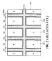
- FIG. 2is schematic view of a conventional continuous wall structure surrounding each red (R), green (G), and blue (B) pixel of a liquid crystal display device;
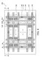
- FIG. 3is a schematic plan view of a liquid crystal device according to an embodiment of the invention.
- FIG. 4is a schematic view of a sub-region 320 of a color filter substrate 310 in FIG. 3 ;
- FIG. 5is a cross section of the continuous wall structure taken along line X-X of FIG. 4 .
- the inventionillustrated by a large scale TFT-LCD panel, is direct to a liquid crystal display device comprising a display region and a non-display region.
- the display regionis divided into a plurality of sub-regions. Each sub-region is surrounded by a continuous insulation wall structure to prevent uneven cell gaps and liquid crystal redistribution due to gravity.
- FIG. 3is a schematic plan view of a liquid crystal device according to an embodiment of the invention.
- a large scale liquid crystal display device 300includes a color filter substrate 310 with a display region 311 a and a non-display region 311 b .
- the display region 311 ais divided into a plurality of sub-regions 320 such as sub-regions A-F.
- the dimension of the sub-regions 320is approximately in a range of 5-15 inches and comprises a plurality of pixels P.
- Each sub-regioncan be square or rectangular, or depending on arrangements of pixels and color filters.
- the arrangements of pixels and color filterscan be striped, mosaic, or honeycomb shapes.
- color filter substrate 310Although the invention is illustrated by color filter substrate 310 , it is, however, not limited thereto. According to another aspect of the invention, a color filter on array (COA) substrate is also applicable.
- COAcolor filter on array
- FIG. 4is a schematic view of a sub-region 320 of a color filter substrate 310 in FIG. 3 .
- the color filter substrate 310is divided into a plurality of sub-regions 320 such as sub-regions A-F.
- One sub-region, such as region Acomprises a transparent substrate 301 , such as a glass substrate or a plastic substrate.
- a black matrix 340is formed on the transparent substrate 301 .
- the black matrix 340can be formed on an opaque region along the periphery or boundary of each pixel region P corresponding to active devices, gate lines and data lines.
- Color filters 330 including red (R) 330 a , green (G) 330 b , and blue (B) 330 care disposed on each pixel region P of the sub-region 320 surrounded by continuous isolation wall structures 355 .
- continuous isolation wall structures 355are not limited to being disposed on the black matrix, and can be disposed on other opaque regions such as gate lines and data lines.
- a passivation layer and a transparent common electrodeare sequentially formed on the color filter substrate.
- spacers 350are formed on the black matrix 340 .
- the spacers 350can provide a uniform and balanced gap between opposing substrates.
- the spacers 350can be columnar spacer structures formed by lithography and etching.
- the inventionprovides a continuous isolation wall structure 355 surrounding each sub-region 320 .
- the continuous isolation wall structure 355 and spacers 350can be formed in the same lithographical etching steps. Alternatively, the continuous isolation wall structure 355 and spacers 350 can be formed separately in different lithographical etching steps.
- the continuous isolation wall structure 355is preferably disposed along the black matrix 340 .
- the width W A of the continuous isolation wall structure 355is less than the width W B of the spacers 320 .
- the height h of the continuous isolation wall structure 355is less than the height H of the spacers 320 , preferably in a range of 1 ⁇ 3-1 ⁇ 4 of the height of the black matrix H.
- FIG. 5is a cross section of the continuous isolation wall structure taken along line X-X of FIG. 4 .
- the color filterscan be alternatively formed on the active matrix substrate.
- the black matrix 340is formed on an opaque region corresponding to active devices, gate lines and data lines.
- Color filters including red (R), green (G), and blue (B)are disposed on each pixel P of the sub-region 320 surrounded by wall isolation structures 355 .
- the wall isolation structures 355are not limited to being disposed on the black matrix, and can be disposed on other opaque regions such as gate lines and data lines.
- a passivation layer and a transparent pixel electrodeare sequentially formed on the active matrix substrate.
- the inventionprovides a large scale LCD device comprising a first substrate and a second substrate parallel and opposing the first substrate with spacers providing a uniform and balanced gap therebetween.
- a plurality of color filtersare formed on the first substrate corresponding to pixel regions.
- a liquid crystal layer formed by one-drop filling (ODF)is interposed between the first substrate and the second substrate.
- the large scale LCD devicefurther comprises a display region 311 a and a non-display region 311 b .
- the display region 311 ais divided into a plurality of sub-regions, and each sub-region is surrounded by continuous isolation wall structures, wherein the height of each continuous isolation wall structure is less than the height of the spacers.
Landscapes
- Physics & Mathematics (AREA)
- Nonlinear Science (AREA)
- Mathematical Physics (AREA)
- Chemical & Material Sciences (AREA)
- Crystallography & Structural Chemistry (AREA)
- General Physics & Mathematics (AREA)
- Optics & Photonics (AREA)
- Liquid Crystal (AREA)
Abstract
Description
- 1. Field of the Invention
- The present invention relates to liquid crystal display (LCD) devices, and in particular to LCD devices with continuous insulation wall structures.
- 2. Description of the Related Art
- Liquid crystal display (LCD) devices have many advantages such as small volume, light weight and low power consumption, and are applicable in a variety of electronic and communication devices including notebook computers, personal digital assistants (PDA), mobile phones and the like. From a fabrication point of view, LCD devices formed by one drop filling (ODF) methods can reduce liquid crystal fill time, and have therefore become main stream methods for fabricating LCD devices.
FIG. 1 is a cross section of a conventional liquid crystal display device. A liquidcrystal display device 100 includes afirst substrate 10, asecond substrate 50, and aliquid crystal layer 70 interposed therebetween. TheLCD device 100 further includes a plurality of pixel regions P defined by the intersection of gate lines (not shown) anddata lines 26. Each pixel region P comprises a region with an active device T such as a thin film transistor (TFT) and apixel electrode 32. The thin film transistor comprises agate 12 electrically connecting the gate line (not shown), asemiconductor layer 20 formed on thegate 12, a source22 formed on thesemiconductor layer 20 connecting thedata line 26 and separating fromdrain 24 by a specific distance.- A
first insulation layer 14 and asecond insulation layer 28 are formed over thefirst substrate 10. A black matrix (BM)52 is formed over the inner surface of thesecond substrate 50 opposing thefirst substrate 10. Theblack matrix 52 is positioned corresponding to the region with active devices T, gate line (not shown), and scanline 26. - The
second substrate 50 further comprisescolor filters 54 on theblack matrix 52. Thecolor filters 54 can be further divided into three color regions such as red (R)54a, green (G)54b, and blue (B)54c. Each color region is positioned corresponding to a pixel region P. Apassivation layer 56 and a transparentcommon electrode 58 are sequentially formed over the inner surface of thesecond substrate 50. Both thefirst substrate 10 andsecond substrate 50 comprise an alignment layer over the inner surface.Spacers 60 are disposed in the liquid crystal layer to maintain a gap between the opposing substrates. - In general, a typical LCD device requires two parallel substrates with a highly precise gap therebetween. Two
substrates liquid crystal 70 is filled into the cavity by vacuum injection, and the cavity is sealed, completing large scale panel devices using vacuum injection, however, is inefficient and lengthy. - In order to improve liquid crystal injection efficiency, a method of one drop filling (ODF) is proposed. After a frame is formed on a flange of a substrate, liquid crystal is directly dripped in the frame region of the substrate. An opposing substrate is subsequently assembled on the substrate. The ODF method, however, usually results in inadequate or excessive liquid crystal being filled, thereby leading to irregular display (mura defects). Moreover, when a large scale TFT-LCD is set upright, distribution of the liquid crystal becomes unbalanced due to gravity causing mura defects. A novel LCD structure is thus required to prevent unbalanced LC distribution and ameliorate mura defects.
- U.S. Publication No. 2004/0263766, the entirety of which is hereby incorporated by reference, discloses a liquid crystal display device as shown in
FIG. 2 . InFIG. 2 , each red (R), green (G) and blue (B) pixel is surrounded by a continuous protrudingwall 108 to serve as spacers. Spacers can prevent unbalanced liquid crystal due to gravity. Thecontinuous protruding wall 108 is disposed on theblack matrix 102. Thecontinuous protruding wall 108, however, may cause isolation of liquid crystal between adjacent pixel regions, and cause further assembly difficulties. - A detailed description is given in the following embodiments with reference to the accompanying drawings.
- The invention is directed to a novel LCD cell structure for an LCD device, which is divided into a plurality of sub-regions. A continuous isolation wall structure is formed surrounding each sub-region to prevent unbalanced liquid crystal distribution.
- In one aspect of the invention, a liquid crystal display device comprises a first substrate with an array of a plurality of pixel regions thereon, a second substrate parallel and opposing the first substrate with a gap therebetween, and a liquid crystal layer interposed between the first substrate and the second substrate, wherein the array is divided into a plurality of sub-regions, and each sub-region comprises a plurality of pixel regions.
- In another aspect of the invention, a liquid crystal display device comprises a first substrate with an array of a plurality of pixel regions thereon, wherein the array is divided into a plurality of sub-regions, and each sub-region comprises a plurality of pixel regions, a plurality of color filters disposed on the first substrate, a second substrate parallel and opposing the first substrate with a gap therebetween, a liquid crystal layer interposed between the first substrate and the second substrate, and a continuous insulation wall structure surrounding the plurality of sub-regions.
- The present invention can be more fully understood by reading the subsequent detailed description and examples with references made to the accompanying drawings, wherein:
FIG. 1 is a cross section of a conventional liquid crystal display device;FIG. 2 is schematic view of a conventional continuous wall structure surrounding each red (R), green (G), and blue (B) pixel of a liquid crystal display device;FIG. 3 is a schematic plan view of a liquid crystal device according to an embodiment of the invention;FIG. 4 is a schematic view of asub-region 320 of acolor filter substrate 310 inFIG. 3 ; andFIG. 5 is a cross section of the continuous wall structure taken along line X-X ofFIG. 4 .- The following description is of the best-contemplated mode of carrying out the invention. This description is made for the purpose of illustrating the general principles of the invention and should not be taken in a limiting sense. The scope of the invention is best determined by reference to the appended claims.
- The invention, illustrated by a large scale TFT-LCD panel, is direct to a liquid crystal display device comprising a display region and a non-display region. The display region is divided into a plurality of sub-regions. Each sub-region is surrounded by a continuous insulation wall structure to prevent uneven cell gaps and liquid crystal redistribution due to gravity.
FIG. 3 is a schematic plan view of a liquid crystal device according to an embodiment of the invention. InFIG. 3 , a large scale liquidcrystal display device 300 includes acolor filter substrate 310 with adisplay region 311aand anon-display region 311b. Thedisplay region 311ais divided into a plurality ofsub-regions 320 such as sub-regions A-F. The dimension of thesub-regions 320 is approximately in a range of 5-15 inches and comprises a plurality of pixels P. Each sub-region can be square or rectangular, or depending on arrangements of pixels and color filters. The arrangements of pixels and color filters can be striped, mosaic, or honeycomb shapes.- Although the invention is illustrated by
color filter substrate 310, it is, however, not limited thereto. According to another aspect of the invention, a color filter on array (COA) substrate is also applicable. FIG. 4 is a schematic view of asub-region 320 of acolor filter substrate 310 inFIG. 3 . Referring toFIG. 4 , thecolor filter substrate 310 is divided into a plurality ofsub-regions 320 such as sub-regions A-F. One sub-region, such as region A, comprises atransparent substrate 301, such as a glass substrate or a plastic substrate. Ablack matrix 340 is formed on thetransparent substrate 301. Theblack matrix 340 can be formed on an opaque region along the periphery or boundary of each pixel region P corresponding to active devices, gate lines and data lines.- Color filters330 including red (R)330a, green (G)330b, and blue (B)330care disposed on each pixel region P of the
sub-region 320 surrounded by continuousisolation wall structures 355. Note that continuousisolation wall structures 355 are not limited to being disposed on the black matrix, and can be disposed on other opaque regions such as gate lines and data lines. A passivation layer and a transparent common electrode are sequentially formed on the color filter substrate. - Subsequently,
spacers 350 are formed on theblack matrix 340. Thespacers 350 can provide a uniform and balanced gap between opposing substrates. Thespacers 350 can be columnar spacer structures formed by lithography and etching. - To prevent mura defects in large scale LCD devices due to gravity, the invention provides a continuous
isolation wall structure 355 surrounding eachsub-region 320. The continuousisolation wall structure 355 andspacers 350 can be formed in the same lithographical etching steps. Alternatively, the continuousisolation wall structure 355 andspacers 350 can be formed separately in different lithographical etching steps. The continuousisolation wall structure 355 is preferably disposed along theblack matrix 340. The width WAof the continuousisolation wall structure 355 is less than the width WBof thespacers 320. The height h of the continuousisolation wall structure 355 is less than the height H of thespacers 320, preferably in a range of ⅓-¼ of the height of the black matrix H. - It should be understood that the height of the continuous isolation wall structure depends on the viscosity of the liquid crystal. If the viscosity of the liquid crystal is high, a lower continuous
isolation wall structure 355 is required. On the contrary, a higher continuousisolation wall structure 355 is required when the viscosity of liquid crystal is high.FIG. 5 is a cross section of the continuous isolation wall structure taken along line X-X ofFIG. 4 . - According another embodiment of the invention, the color filters can be alternatively formed on the active matrix substrate. The
black matrix 340 is formed on an opaque region corresponding to active devices, gate lines and data lines. Color filters including red (R), green (G), and blue (B) are disposed on each pixel P of thesub-region 320 surrounded bywall isolation structures 355. Note that thewall isolation structures 355 are not limited to being disposed on the black matrix, and can be disposed on other opaque regions such as gate lines and data lines. A passivation layer and a transparent pixel electrode are sequentially formed on the active matrix substrate. - Accordingly, the invention provides a large scale LCD device comprising a first substrate and a second substrate parallel and opposing the first substrate with spacers providing a uniform and balanced gap therebetween. A plurality of color filters are formed on the first substrate corresponding to pixel regions. A liquid crystal layer formed by one-drop filling (ODF) is interposed between the first substrate and the second substrate. The large scale LCD device further comprises a
display region 311aand anon-display region 311b. Thedisplay region 311ais divided into a plurality of sub-regions, and each sub-region is surrounded by continuous isolation wall structures, wherein the height of each continuous isolation wall structure is less than the height of the spacers. - The invention is advantageous in that by dividing a large scale LCD into a plurality of sub-regions surrounded by a continuous isolation wall structure prevents the effect of gravity on the liquid crystal thereby ameliorating mura defects
- While the invention has been described by way of example and in terms of the preferred embodiments, it is to be understood that the invention is not limited to the disclosed embodiments. To the contrary, it is intended to cover various modifications and similar arrangements (as would be apparent to those skilled in the art). Therefore, the scope of the appended claims should be accorded the broadest interpretation so as to encompass all such modifications and similar arrangements.
Claims (19)
1. A liquid crystal display device, comprising:
a first substrate with an array of a plurality of pixel regions thereon;
a second substrate parallel and opposing the first substrate with a gap therebetween; and
a liquid crystal layer interposed between the first substrate and the second substrate,
wherein the array is divided into a plurality of sub-regions, and each sub-region comprises a plurality of pixel regions.
2. The liquid crystal display device as claimed inclaim 1 , further comprising a plurality of color filters disposed on the first substrate.
3. The liquid crystal display device as claimed inclaim 2 , further comprising a black matrix disposed on a peripheral region of each color filter layer.
4. The liquid crystal display device as claimed inclaim 1 , further comprising an array of active devices on the first substrate.
5. The liquid crystal display device as claimed inclaim 4 , wherein the array of active devices is composed of a plurality of gate lines and a plurality of data lines.
6. The liquid crystal display device as claimed inclaim 1 , between the first substrate and the second substrate, further comprising a plurality of spacers.
7. The liquid crystal display device as claimed inclaim 6 , further comprising an insulation wall structure surrounding the plurality of sub-regions.
8. The liquid crystal display device as claimed inclaim 7 , wherein a height of the continuous insulation wall structure is approximately ⅓-⅘ of the height of the plurality of spacers.
9. The liquid crystal display device as claimed inclaim 7 , wherein the insulation wall structure is disposed on a black matrix between each color filter layer.
10. The liquid crystal display device as claimed inclaim 7 , wherein the continuous insulation wall structure is disposed on the gate lines and the data lines of the array of the active devices.
11. The liquid crystal display device as claimed inclaim 1 , wherein the dimensions of the sub-regions is approximately in a range of 5-15 inches.
12. The liquid crystal display device as claimed inclaim 1 , wherein the liquid crystal layer is formed by a one-drop filling (ODF) method.
13. A liquid crystal display device, comprising:
a first substrate with an array of a plurality of pixel regions thereon, wherein the array is divided into a plurality of sub-regions, and each sub-region comprises a plurality of pixel regions;
a plurality of color filters disposed on the first substrate;
a second substrate parallel and opposing the first substrate with a gap therebetween;
a liquid crystal layer interposed between the first substrate and the second substrate; and
a continuous insulation wall structure surrounding the plurality of sub-regions.
14. The liquid crystal display device as claimed inclaim 13 , further comprising a black matrix disposed on a peripheral region of each color filter layer.
15. The liquid crystal display device as claimed inclaim 13 , between the first substrate and the second substrate, further comprising a plurality of spacers.
16. The liquid crystal display device as claimed inclaim 15 , wherein a height of the continuous insulation wall structure is approximately ⅓-⅘ of the height of the plurality of spacers.
17. The liquid crystal display device as claimed inclaim 13 , wherein the continuous insulation wall structure is disposed on a black matrix.
18. The liquid crystal display device as claimed inclaim 13 , wherein the dimensions of the sub-regions is approximately in a range of 5-15 inches.
19. The liquid crystal display device as claimed inclaim 13 , wherein the liquid crystal layer is formed by a one-drop filling (ODF) method.
Applications Claiming Priority (2)
| Application Number | Priority Date | Filing Date | Title |
|---|---|---|---|
| TW94146694 | 2005-12-27 | ||
| TW094146694ATWI321675B (en) | 2005-12-27 | 2005-12-27 | Liquid crystal display panel |
Publications (2)
| Publication Number | Publication Date |
|---|---|
| US20070146619A1true US20070146619A1 (en) | 2007-06-28 |
| US7580105B2 US7580105B2 (en) | 2009-08-25 |
Family
ID=38193212
Family Applications (1)
| Application Number | Title | Priority Date | Filing Date |
|---|---|---|---|
| US11/419,215Active2027-04-14US7580105B2 (en) | 2005-12-27 | 2006-05-19 | Liquid crystal display devices |
Country Status (4)
| Country | Link |
|---|---|
| US (1) | US7580105B2 (en) |
| JP (1) | JP4495139B2 (en) |
| KR (1) | KR100794886B1 (en) |
| TW (1) | TWI321675B (en) |
Cited By (3)
| Publication number | Priority date | Publication date | Assignee | Title |
|---|---|---|---|---|
| CN106054435A (en)* | 2016-08-18 | 2016-10-26 | 京东方科技集团股份有限公司 | Pair box substrate, liquid crystal display panel and bright spot eliminating method thereof |
| EP3153916A1 (en)* | 2015-10-06 | 2017-04-12 | LG Display Co., Ltd. | Light control device for a transparent display and method of manufacturing the device |
| CN114942536A (en)* | 2022-07-26 | 2022-08-26 | 惠科股份有限公司 | Liquid crystal display module and electronic device |
Families Citing this family (5)
| Publication number | Priority date | Publication date | Assignee | Title |
|---|---|---|---|---|
| JP2017015787A (en)* | 2015-06-26 | 2017-01-19 | パナソニック液晶ディスプレイ株式会社 | Liquid crystal display |
| KR102568789B1 (en)* | 2016-03-10 | 2023-08-21 | 삼성전자주식회사 | Filter array including an inorganic color filter, and image sensor and display apparatus including the filter arrary |
| KR102060127B1 (en) | 2019-09-10 | 2019-12-27 | 유지씨 주식회사 | Repair unit for repairing leaks generated around the periphery of window frames and repair method using the repair unit |
| US11571047B2 (en) | 2020-06-03 | 2023-02-07 | Hornling Industrial Inc. | Latching mechanism |
| WO2025134651A1 (en)* | 2023-12-20 | 2025-06-26 | ソニーグループ株式会社 | Spatial light modulator and display device |
Citations (1)
| Publication number | Priority date | Publication date | Assignee | Title |
|---|---|---|---|---|
| US20030128327A1 (en)* | 2002-01-10 | 2003-07-10 | Nec Corporation | Liquid crystal display panel and manufacturing method thereof |
Family Cites Families (10)
| Publication number | Priority date | Publication date | Assignee | Title |
|---|---|---|---|---|
| JPS5115876U (en)* | 1974-07-22 | 1976-02-05 | ||
| JPH01271726A (en)* | 1988-04-25 | 1989-10-30 | Mitsubishi Electric Corp | liquid crystal display element |
| JPH0545661A (en)* | 1991-08-21 | 1993-02-26 | Toshiba Corp | Production of liquid crystal display panel |
| JP3291863B2 (en)* | 1993-09-16 | 2002-06-17 | 凸版印刷株式会社 | LCD panel |
| JPH07128640A (en)* | 1993-10-29 | 1995-05-19 | Sharp Corp | Ferroelectric liquid crystal display device |
| JP3492203B2 (en) | 1998-06-25 | 2004-02-03 | 松下電器産業株式会社 | Liquid crystal display |
| JP2003066463A (en)* | 2001-08-28 | 2003-03-05 | Citizen Watch Co Ltd | Liquid crystal display device |
| KR20040012303A (en) | 2002-08-02 | 2004-02-11 | 삼성전자주식회사 | a panel for a liquid crystal display, a liquid crystal display including the panel, and a methods for manufacturing the same |
| US8125601B2 (en)* | 2003-01-08 | 2012-02-28 | Samsung Electronics Co., Ltd. | Upper substrate and liquid crystal display device having the same |
| KR20050001158A (en)* | 2003-06-27 | 2005-01-06 | 엘지.필립스 엘시디 주식회사 | LCD with a column spacer and method for fabricating the same |
- 2005
- 2005-12-27TWTW094146694Apatent/TWI321675B/ennot_activeIP Right Cessation
- 2006
- 2006-05-19USUS11/419,215patent/US7580105B2/enactiveActive
- 2006-05-29KRKR1020060047911Apatent/KR100794886B1/ennot_activeExpired - Fee Related
- 2006-12-19JPJP2006340677Apatent/JP4495139B2/enactiveActive
Patent Citations (1)
| Publication number | Priority date | Publication date | Assignee | Title |
|---|---|---|---|---|
| US20030128327A1 (en)* | 2002-01-10 | 2003-07-10 | Nec Corporation | Liquid crystal display panel and manufacturing method thereof |
Cited By (6)
| Publication number | Priority date | Publication date | Assignee | Title |
|---|---|---|---|---|
| EP3153916A1 (en)* | 2015-10-06 | 2017-04-12 | LG Display Co., Ltd. | Light control device for a transparent display and method of manufacturing the device |
| US10126583B2 (en) | 2015-10-06 | 2018-11-13 | Lg Display Co., Ltd. | Light controlling device, transparent display device including the same, and method for fabricating the same |
| CN106054435A (en)* | 2016-08-18 | 2016-10-26 | 京东方科技集团股份有限公司 | Pair box substrate, liquid crystal display panel and bright spot eliminating method thereof |
| US20190056614A1 (en)* | 2016-08-18 | 2019-02-21 | Boe Technology Group Co., Ltd. | Counter substrate, liquid crystal display panel and method for eliminating bright spots |
| CN114942536A (en)* | 2022-07-26 | 2022-08-26 | 惠科股份有限公司 | Liquid crystal display module and electronic device |
| US11763765B1 (en) | 2022-07-26 | 2023-09-19 | HKC Corporation Limited | Liquid crystal display assembly and electronic device |
Also Published As
| Publication number | Publication date |
|---|---|
| TWI321675B (en) | 2010-03-11 |
| JP4495139B2 (en) | 2010-06-30 |
| US7580105B2 (en) | 2009-08-25 |
| JP2007179051A (en) | 2007-07-12 |
| KR20070068987A (en) | 2007-07-02 |
| TW200725041A (en) | 2007-07-01 |
| KR100794886B1 (en) | 2008-01-14 |
Similar Documents
| Publication | Publication Date | Title |
|---|---|---|
| US10423039B2 (en) | Array substrate and manufacturing method thereof | |
| CN110824786B (en) | Display panel and display device | |
| US8379180B2 (en) | Liquid crystal display panel and manufacturing method of opposite substrate thereof | |
| US7580105B2 (en) | Liquid crystal display devices | |
| KR100675635B1 (en) | Transverse field mode liquid crystal display with improved contrast ratio | |
| KR101031166B1 (en) | Liquid crystal display panel | |
| CN107688254B (en) | COA type liquid crystal display panel and manufacturing method thereof | |
| GB2408622A (en) | Color filter array substrate and fabricating method thereof | |
| US20190049804A1 (en) | Active switch array substrate, manufacturing method therfor, and display panel | |
| US8194225B2 (en) | Array substrate for LCD device | |
| CN102508376A (en) | Liquid crystal display panel and manufacturing method thereof | |
| CN207817366U (en) | A kind of color membrane substrates, display panel and display device | |
| US6897931B2 (en) | In-plane switching mode liquid crystal display device and method for fabricating the same | |
| US12164187B2 (en) | Display substrate and display panel in each of which distance from convex structure to a substrate and distance from alignment layer to the substrate has preset difference therebetween | |
| CN106405964A (en) | Array substrate, manufacturing method thereof and LCD (Liquid Crystal Display) | |
| US20190049803A1 (en) | Active switch array substrate, manufacturing method therefor same, and display device using same | |
| US20070109486A1 (en) | Liquid crystal display panel | |
| CN112666742A (en) | Liquid crystal display panel and display device | |
| CN114077108B (en) | A display panel and display device | |
| CN112445017B (en) | Color filter substrate and forming method thereof | |
| US7646467B2 (en) | Method of fabricating liquid crystal display devices having various driving modes on a common substrate | |
| CN109541859B (en) | Liquid crystal display panel and method for manufacturing the same | |
| CN1794046A (en) | Liquid crystal display device | |
| US20070052910A1 (en) | Liquid crystal display panel | |
| US8274636B2 (en) | Method for forming spacers on substrate |
Legal Events
| Date | Code | Title | Description |
|---|---|---|---|
| AS | Assignment | Owner name:QUANTA DISPLAY INC., TAIWAN Free format text:ASSIGNMENT OF ASSIGNORS INTEREST;ASSIGNOR:SHYU, WEN-YIH;REEL/FRAME:017641/0357 Effective date:20060505 | |
| AS | Assignment | Owner name:AU OPTRONICS CORP.,TAIWAN Free format text:MERGER;ASSIGNOR:QUANTA DISPLAY, INC.;REEL/FRAME:019032/0801 Effective date:20060623 Owner name:AU OPTRONICS CORP., TAIWAN Free format text:MERGER;ASSIGNOR:QUANTA DISPLAY, INC.;REEL/FRAME:019032/0801 Effective date:20060623 | |
| STCF | Information on status: patent grant | Free format text:PATENTED CASE | |
| FPAY | Fee payment | Year of fee payment:4 | |
| FPAY | Fee payment | Year of fee payment:8 | |
| MAFP | Maintenance fee payment | Free format text:PAYMENT OF MAINTENANCE FEE, 12TH YEAR, LARGE ENTITY (ORIGINAL EVENT CODE: M1553); ENTITY STATUS OF PATENT OWNER: LARGE ENTITY Year of fee payment:12 |