US20070145558A1 - Super high density module with integrated wafer level packages - Google Patents
Super high density module with integrated wafer level packagesDownload PDFInfo
- Publication number
- US20070145558A1 US20070145558A1US11/712,152US71215207AUS2007145558A1US 20070145558 A1US20070145558 A1US 20070145558A1US 71215207 AUS71215207 AUS 71215207AUS 2007145558 A1US2007145558 A1US 2007145558A1
- Authority
- US
- United States
- Prior art keywords
- die
- insulating layer
- trace
- dies
- pad
- Prior art date
- Legal status (The legal status is an assumption and is not a legal conclusion. Google has not performed a legal analysis and makes no representation as to the accuracy of the status listed.)
- Granted
Links
Images


Classifications
- H—ELECTRICITY
- H01—ELECTRIC ELEMENTS
- H01L—SEMICONDUCTOR DEVICES NOT COVERED BY CLASS H10
- H01L24/00—Arrangements for connecting or disconnecting semiconductor or solid-state bodies; Methods or apparatus related thereto
- H01L24/01—Means for bonding being attached to, or being formed on, the surface to be connected, e.g. chip-to-package, die-attach, "first-level" interconnects; Manufacturing methods related thereto
- H01L24/10—Bump connectors ; Manufacturing methods related thereto
- H—ELECTRICITY
- H01—ELECTRIC ELEMENTS
- H01L—SEMICONDUCTOR DEVICES NOT COVERED BY CLASS H10
- H01L23/00—Details of semiconductor or other solid state devices
- H01L23/28—Encapsulations, e.g. encapsulating layers, coatings, e.g. for protection
- H01L23/31—Encapsulations, e.g. encapsulating layers, coatings, e.g. for protection characterised by the arrangement or shape
- H01L23/3107—Encapsulations, e.g. encapsulating layers, coatings, e.g. for protection characterised by the arrangement or shape the device being completely enclosed
- H01L23/3114—Encapsulations, e.g. encapsulating layers, coatings, e.g. for protection characterised by the arrangement or shape the device being completely enclosed the device being a chip scale package, e.g. CSP
- H—ELECTRICITY
- H01—ELECTRIC ELEMENTS
- H01L—SEMICONDUCTOR DEVICES NOT COVERED BY CLASS H10
- H01L23/00—Details of semiconductor or other solid state devices
- H01L23/52—Arrangements for conducting electric current within the device in operation from one component to another, i.e. interconnections, e.g. wires, lead frames
- H01L23/522—Arrangements for conducting electric current within the device in operation from one component to another, i.e. interconnections, e.g. wires, lead frames including external interconnections consisting of a multilayer structure of conductive and insulating layers inseparably formed on the semiconductor body
- H01L23/525—Arrangements for conducting electric current within the device in operation from one component to another, i.e. interconnections, e.g. wires, lead frames including external interconnections consisting of a multilayer structure of conductive and insulating layers inseparably formed on the semiconductor body with adaptable interconnections
- H—ELECTRICITY
- H01—ELECTRIC ELEMENTS
- H01L—SEMICONDUCTOR DEVICES NOT COVERED BY CLASS H10
- H01L23/00—Details of semiconductor or other solid state devices
- H01L23/52—Arrangements for conducting electric current within the device in operation from one component to another, i.e. interconnections, e.g. wires, lead frames
- H01L23/538—Arrangements for conducting electric current within the device in operation from one component to another, i.e. interconnections, e.g. wires, lead frames the interconnection structure between a plurality of semiconductor chips being formed on, or in, insulating substrates
- H01L23/5389—Arrangements for conducting electric current within the device in operation from one component to another, i.e. interconnections, e.g. wires, lead frames the interconnection structure between a plurality of semiconductor chips being formed on, or in, insulating substrates the chips being integrally enclosed by the interconnect and support structures
- H—ELECTRICITY
- H01—ELECTRIC ELEMENTS
- H01L—SEMICONDUCTOR DEVICES NOT COVERED BY CLASS H10
- H01L24/00—Arrangements for connecting or disconnecting semiconductor or solid-state bodies; Methods or apparatus related thereto
- H01L24/01—Means for bonding being attached to, or being formed on, the surface to be connected, e.g. chip-to-package, die-attach, "first-level" interconnects; Manufacturing methods related thereto
- H01L24/02—Bonding areas ; Manufacturing methods related thereto
- H—ELECTRICITY
- H01—ELECTRIC ELEMENTS
- H01L—SEMICONDUCTOR DEVICES NOT COVERED BY CLASS H10
- H01L25/00—Assemblies consisting of a plurality of semiconductor or other solid state devices
- H01L25/03—Assemblies consisting of a plurality of semiconductor or other solid state devices all the devices being of a type provided for in a single subclass of subclasses H10B, H10D, H10F, H10H, H10K or H10N, e.g. assemblies of rectifier diodes
- H01L25/04—Assemblies consisting of a plurality of semiconductor or other solid state devices all the devices being of a type provided for in a single subclass of subclasses H10B, H10D, H10F, H10H, H10K or H10N, e.g. assemblies of rectifier diodes the devices not having separate containers
- H01L25/065—Assemblies consisting of a plurality of semiconductor or other solid state devices all the devices being of a type provided for in a single subclass of subclasses H10B, H10D, H10F, H10H, H10K or H10N, e.g. assemblies of rectifier diodes the devices not having separate containers the devices being of a type provided for in group H10D89/00
- H01L25/0655—Assemblies consisting of a plurality of semiconductor or other solid state devices all the devices being of a type provided for in a single subclass of subclasses H10B, H10D, H10F, H10H, H10K or H10N, e.g. assemblies of rectifier diodes the devices not having separate containers the devices being of a type provided for in group H10D89/00 the devices being arranged next to each other
- H—ELECTRICITY
- H01—ELECTRIC ELEMENTS
- H01L—SEMICONDUCTOR DEVICES NOT COVERED BY CLASS H10
- H01L2224/00—Indexing scheme for arrangements for connecting or disconnecting semiconductor or solid-state bodies and methods related thereto as covered by H01L24/00
- H01L2224/01—Means for bonding being attached to, or being formed on, the surface to be connected, e.g. chip-to-package, die-attach, "first-level" interconnects; Manufacturing methods related thereto
- H01L2224/02—Bonding areas; Manufacturing methods related thereto
- H01L2224/023—Redistribution layers [RDL] for bonding areas
- H01L2224/0237—Disposition of the redistribution layers
- H01L2224/02379—Fan-out arrangement
- H—ELECTRICITY
- H01—ELECTRIC ELEMENTS
- H01L—SEMICONDUCTOR DEVICES NOT COVERED BY CLASS H10
- H01L2224/00—Indexing scheme for arrangements for connecting or disconnecting semiconductor or solid-state bodies and methods related thereto as covered by H01L24/00
- H01L2224/01—Means for bonding being attached to, or being formed on, the surface to be connected, e.g. chip-to-package, die-attach, "first-level" interconnects; Manufacturing methods related thereto
- H01L2224/02—Bonding areas; Manufacturing methods related thereto
- H01L2224/04—Structure, shape, material or disposition of the bonding areas prior to the connecting process
- H01L2224/05—Structure, shape, material or disposition of the bonding areas prior to the connecting process of an individual bonding area
- H01L2224/05001—Internal layers
- H01L2224/0502—Disposition
- H01L2224/05024—Disposition the internal layer being disposed on a redistribution layer on the semiconductor or solid-state body
- H—ELECTRICITY
- H01—ELECTRIC ELEMENTS
- H01L—SEMICONDUCTOR DEVICES NOT COVERED BY CLASS H10
- H01L2224/00—Indexing scheme for arrangements for connecting or disconnecting semiconductor or solid-state bodies and methods related thereto as covered by H01L24/00
- H01L2224/01—Means for bonding being attached to, or being formed on, the surface to be connected, e.g. chip-to-package, die-attach, "first-level" interconnects; Manufacturing methods related thereto
- H01L2224/02—Bonding areas; Manufacturing methods related thereto
- H01L2224/04—Structure, shape, material or disposition of the bonding areas prior to the connecting process
- H01L2224/05—Structure, shape, material or disposition of the bonding areas prior to the connecting process of an individual bonding area
- H01L2224/05001—Internal layers
- H01L2224/0502—Disposition
- H01L2224/05026—Disposition the internal layer being disposed in a recess of the surface
- H—ELECTRICITY
- H01—ELECTRIC ELEMENTS
- H01L—SEMICONDUCTOR DEVICES NOT COVERED BY CLASS H10
- H01L2224/00—Indexing scheme for arrangements for connecting or disconnecting semiconductor or solid-state bodies and methods related thereto as covered by H01L24/00
- H01L2224/01—Means for bonding being attached to, or being formed on, the surface to be connected, e.g. chip-to-package, die-attach, "first-level" interconnects; Manufacturing methods related thereto
- H01L2224/02—Bonding areas; Manufacturing methods related thereto
- H01L2224/04—Structure, shape, material or disposition of the bonding areas prior to the connecting process
- H01L2224/05—Structure, shape, material or disposition of the bonding areas prior to the connecting process of an individual bonding area
- H01L2224/05001—Internal layers
- H01L2224/05099—Material
- H01L2224/051—Material with a principal constituent of the material being a metal or a metalloid, e.g. boron [B], silicon [Si], germanium [Ge], arsenic [As], antimony [Sb], tellurium [Te] and polonium [Po], and alloys thereof
- H01L2224/05117—Material with a principal constituent of the material being a metal or a metalloid, e.g. boron [B], silicon [Si], germanium [Ge], arsenic [As], antimony [Sb], tellurium [Te] and polonium [Po], and alloys thereof the principal constituent melting at a temperature of greater than or equal to 400°C and less than 950°C
- H01L2224/05124—Aluminium [Al] as principal constituent
- H—ELECTRICITY
- H01—ELECTRIC ELEMENTS
- H01L—SEMICONDUCTOR DEVICES NOT COVERED BY CLASS H10
- H01L2224/00—Indexing scheme for arrangements for connecting or disconnecting semiconductor or solid-state bodies and methods related thereto as covered by H01L24/00
- H01L2224/01—Means for bonding being attached to, or being formed on, the surface to be connected, e.g. chip-to-package, die-attach, "first-level" interconnects; Manufacturing methods related thereto
- H01L2224/02—Bonding areas; Manufacturing methods related thereto
- H01L2224/04—Structure, shape, material or disposition of the bonding areas prior to the connecting process
- H01L2224/05—Structure, shape, material or disposition of the bonding areas prior to the connecting process of an individual bonding area
- H01L2224/05001—Internal layers
- H01L2224/05099—Material
- H01L2224/051—Material with a principal constituent of the material being a metal or a metalloid, e.g. boron [B], silicon [Si], germanium [Ge], arsenic [As], antimony [Sb], tellurium [Te] and polonium [Po], and alloys thereof
- H01L2224/05138—Material with a principal constituent of the material being a metal or a metalloid, e.g. boron [B], silicon [Si], germanium [Ge], arsenic [As], antimony [Sb], tellurium [Te] and polonium [Po], and alloys thereof the principal constituent melting at a temperature of greater than or equal to 950°C and less than 1550°C
- H01L2224/05147—Copper [Cu] as principal constituent
- H—ELECTRICITY
- H01—ELECTRIC ELEMENTS
- H01L—SEMICONDUCTOR DEVICES NOT COVERED BY CLASS H10
- H01L2224/00—Indexing scheme for arrangements for connecting or disconnecting semiconductor or solid-state bodies and methods related thereto as covered by H01L24/00
- H01L2224/01—Means for bonding being attached to, or being formed on, the surface to be connected, e.g. chip-to-package, die-attach, "first-level" interconnects; Manufacturing methods related thereto
- H01L2224/02—Bonding areas; Manufacturing methods related thereto
- H01L2224/04—Structure, shape, material or disposition of the bonding areas prior to the connecting process
- H01L2224/05—Structure, shape, material or disposition of the bonding areas prior to the connecting process of an individual bonding area
- H01L2224/05001—Internal layers
- H01L2224/05099—Material
- H01L2224/051—Material with a principal constituent of the material being a metal or a metalloid, e.g. boron [B], silicon [Si], germanium [Ge], arsenic [As], antimony [Sb], tellurium [Te] and polonium [Po], and alloys thereof
- H01L2224/05163—Material with a principal constituent of the material being a metal or a metalloid, e.g. boron [B], silicon [Si], germanium [Ge], arsenic [As], antimony [Sb], tellurium [Te] and polonium [Po], and alloys thereof the principal constituent melting at a temperature of greater than 1550°C
- H01L2224/05166—Titanium [Ti] as principal constituent
- H—ELECTRICITY
- H01—ELECTRIC ELEMENTS
- H01L—SEMICONDUCTOR DEVICES NOT COVERED BY CLASS H10
- H01L2224/00—Indexing scheme for arrangements for connecting or disconnecting semiconductor or solid-state bodies and methods related thereto as covered by H01L24/00
- H01L2224/01—Means for bonding being attached to, or being formed on, the surface to be connected, e.g. chip-to-package, die-attach, "first-level" interconnects; Manufacturing methods related thereto
- H01L2224/02—Bonding areas; Manufacturing methods related thereto
- H01L2224/04—Structure, shape, material or disposition of the bonding areas prior to the connecting process
- H01L2224/05—Structure, shape, material or disposition of the bonding areas prior to the connecting process of an individual bonding area
- H01L2224/05001—Internal layers
- H01L2224/05099—Material
- H01L2224/051—Material with a principal constituent of the material being a metal or a metalloid, e.g. boron [B], silicon [Si], germanium [Ge], arsenic [As], antimony [Sb], tellurium [Te] and polonium [Po], and alloys thereof
- H01L2224/05163—Material with a principal constituent of the material being a metal or a metalloid, e.g. boron [B], silicon [Si], germanium [Ge], arsenic [As], antimony [Sb], tellurium [Te] and polonium [Po], and alloys thereof the principal constituent melting at a temperature of greater than 1550°C
- H01L2224/05169—Platinum [Pt] as principal constituent
- H—ELECTRICITY
- H01—ELECTRIC ELEMENTS
- H01L—SEMICONDUCTOR DEVICES NOT COVERED BY CLASS H10
- H01L2224/00—Indexing scheme for arrangements for connecting or disconnecting semiconductor or solid-state bodies and methods related thereto as covered by H01L24/00
- H01L2224/01—Means for bonding being attached to, or being formed on, the surface to be connected, e.g. chip-to-package, die-attach, "first-level" interconnects; Manufacturing methods related thereto
- H01L2224/02—Bonding areas; Manufacturing methods related thereto
- H01L2224/04—Structure, shape, material or disposition of the bonding areas prior to the connecting process
- H01L2224/05—Structure, shape, material or disposition of the bonding areas prior to the connecting process of an individual bonding area
- H01L2224/05001—Internal layers
- H01L2224/05099—Material
- H01L2224/051—Material with a principal constituent of the material being a metal or a metalloid, e.g. boron [B], silicon [Si], germanium [Ge], arsenic [As], antimony [Sb], tellurium [Te] and polonium [Po], and alloys thereof
- H01L2224/05163—Material with a principal constituent of the material being a metal or a metalloid, e.g. boron [B], silicon [Si], germanium [Ge], arsenic [As], antimony [Sb], tellurium [Te] and polonium [Po], and alloys thereof the principal constituent melting at a temperature of greater than 1550°C
- H01L2224/05181—Tantalum [Ta] as principal constituent
- H—ELECTRICITY
- H01—ELECTRIC ELEMENTS
- H01L—SEMICONDUCTOR DEVICES NOT COVERED BY CLASS H10
- H01L2224/00—Indexing scheme for arrangements for connecting or disconnecting semiconductor or solid-state bodies and methods related thereto as covered by H01L24/00
- H01L2224/01—Means for bonding being attached to, or being formed on, the surface to be connected, e.g. chip-to-package, die-attach, "first-level" interconnects; Manufacturing methods related thereto
- H01L2224/02—Bonding areas; Manufacturing methods related thereto
- H01L2224/04—Structure, shape, material or disposition of the bonding areas prior to the connecting process
- H01L2224/05—Structure, shape, material or disposition of the bonding areas prior to the connecting process of an individual bonding area
- H01L2224/05001—Internal layers
- H01L2224/05099—Material
- H01L2224/051—Material with a principal constituent of the material being a metal or a metalloid, e.g. boron [B], silicon [Si], germanium [Ge], arsenic [As], antimony [Sb], tellurium [Te] and polonium [Po], and alloys thereof
- H01L2224/05163—Material with a principal constituent of the material being a metal or a metalloid, e.g. boron [B], silicon [Si], germanium [Ge], arsenic [As], antimony [Sb], tellurium [Te] and polonium [Po], and alloys thereof the principal constituent melting at a temperature of greater than 1550°C
- H01L2224/05184—Tungsten [W] as principal constituent
- H—ELECTRICITY
- H01—ELECTRIC ELEMENTS
- H01L—SEMICONDUCTOR DEVICES NOT COVERED BY CLASS H10
- H01L2224/00—Indexing scheme for arrangements for connecting or disconnecting semiconductor or solid-state bodies and methods related thereto as covered by H01L24/00
- H01L2224/01—Means for bonding being attached to, or being formed on, the surface to be connected, e.g. chip-to-package, die-attach, "first-level" interconnects; Manufacturing methods related thereto
- H01L2224/02—Bonding areas; Manufacturing methods related thereto
- H01L2224/04—Structure, shape, material or disposition of the bonding areas prior to the connecting process
- H01L2224/05—Structure, shape, material or disposition of the bonding areas prior to the connecting process of an individual bonding area
- H01L2224/0554—External layer
- H01L2224/05541—Structure
- H01L2224/05548—Bonding area integrally formed with a redistribution layer on the semiconductor or solid-state body
- H—ELECTRICITY
- H01—ELECTRIC ELEMENTS
- H01L—SEMICONDUCTOR DEVICES NOT COVERED BY CLASS H10
- H01L2224/00—Indexing scheme for arrangements for connecting or disconnecting semiconductor or solid-state bodies and methods related thereto as covered by H01L24/00
- H01L2224/01—Means for bonding being attached to, or being formed on, the surface to be connected, e.g. chip-to-package, die-attach, "first-level" interconnects; Manufacturing methods related thereto
- H01L2224/02—Bonding areas; Manufacturing methods related thereto
- H01L2224/04—Structure, shape, material or disposition of the bonding areas prior to the connecting process
- H01L2224/05—Structure, shape, material or disposition of the bonding areas prior to the connecting process of an individual bonding area
- H01L2224/0554—External layer
- H01L2224/05599—Material
- H01L2224/056—Material with a principal constituent of the material being a metal or a metalloid, e.g. boron [B], silicon [Si], germanium [Ge], arsenic [As], antimony [Sb], tellurium [Te] and polonium [Po], and alloys thereof
- H01L2224/05617—Material with a principal constituent of the material being a metal or a metalloid, e.g. boron [B], silicon [Si], germanium [Ge], arsenic [As], antimony [Sb], tellurium [Te] and polonium [Po], and alloys thereof the principal constituent melting at a temperature of greater than or equal to 400°C and less than 950°C
- H01L2224/05624—Aluminium [Al] as principal constituent
- H—ELECTRICITY
- H01—ELECTRIC ELEMENTS
- H01L—SEMICONDUCTOR DEVICES NOT COVERED BY CLASS H10
- H01L2224/00—Indexing scheme for arrangements for connecting or disconnecting semiconductor or solid-state bodies and methods related thereto as covered by H01L24/00
- H01L2224/01—Means for bonding being attached to, or being formed on, the surface to be connected, e.g. chip-to-package, die-attach, "first-level" interconnects; Manufacturing methods related thereto
- H01L2224/02—Bonding areas; Manufacturing methods related thereto
- H01L2224/04—Structure, shape, material or disposition of the bonding areas prior to the connecting process
- H01L2224/05—Structure, shape, material or disposition of the bonding areas prior to the connecting process of an individual bonding area
- H01L2224/0554—External layer
- H01L2224/05599—Material
- H01L2224/056—Material with a principal constituent of the material being a metal or a metalloid, e.g. boron [B], silicon [Si], germanium [Ge], arsenic [As], antimony [Sb], tellurium [Te] and polonium [Po], and alloys thereof
- H01L2224/05638—Material with a principal constituent of the material being a metal or a metalloid, e.g. boron [B], silicon [Si], germanium [Ge], arsenic [As], antimony [Sb], tellurium [Te] and polonium [Po], and alloys thereof the principal constituent melting at a temperature of greater than or equal to 950°C and less than 1550°C
- H01L2224/05644—Gold [Au] as principal constituent
- H—ELECTRICITY
- H01—ELECTRIC ELEMENTS
- H01L—SEMICONDUCTOR DEVICES NOT COVERED BY CLASS H10
- H01L2224/00—Indexing scheme for arrangements for connecting or disconnecting semiconductor or solid-state bodies and methods related thereto as covered by H01L24/00
- H01L2224/01—Means for bonding being attached to, or being formed on, the surface to be connected, e.g. chip-to-package, die-attach, "first-level" interconnects; Manufacturing methods related thereto
- H01L2224/02—Bonding areas; Manufacturing methods related thereto
- H01L2224/04—Structure, shape, material or disposition of the bonding areas prior to the connecting process
- H01L2224/05—Structure, shape, material or disposition of the bonding areas prior to the connecting process of an individual bonding area
- H01L2224/0554—External layer
- H01L2224/05599—Material
- H01L2224/056—Material with a principal constituent of the material being a metal or a metalloid, e.g. boron [B], silicon [Si], germanium [Ge], arsenic [As], antimony [Sb], tellurium [Te] and polonium [Po], and alloys thereof
- H01L2224/05638—Material with a principal constituent of the material being a metal or a metalloid, e.g. boron [B], silicon [Si], germanium [Ge], arsenic [As], antimony [Sb], tellurium [Te] and polonium [Po], and alloys thereof the principal constituent melting at a temperature of greater than or equal to 950°C and less than 1550°C
- H01L2224/05647—Copper [Cu] as principal constituent
- H—ELECTRICITY
- H01—ELECTRIC ELEMENTS
- H01L—SEMICONDUCTOR DEVICES NOT COVERED BY CLASS H10
- H01L2224/00—Indexing scheme for arrangements for connecting or disconnecting semiconductor or solid-state bodies and methods related thereto as covered by H01L24/00
- H01L2224/01—Means for bonding being attached to, or being formed on, the surface to be connected, e.g. chip-to-package, die-attach, "first-level" interconnects; Manufacturing methods related thereto
- H01L2224/02—Bonding areas; Manufacturing methods related thereto
- H01L2224/04—Structure, shape, material or disposition of the bonding areas prior to the connecting process
- H01L2224/05—Structure, shape, material or disposition of the bonding areas prior to the connecting process of an individual bonding area
- H01L2224/0554—External layer
- H01L2224/05599—Material
- H01L2224/056—Material with a principal constituent of the material being a metal or a metalloid, e.g. boron [B], silicon [Si], germanium [Ge], arsenic [As], antimony [Sb], tellurium [Te] and polonium [Po], and alloys thereof
- H01L2224/05638—Material with a principal constituent of the material being a metal or a metalloid, e.g. boron [B], silicon [Si], germanium [Ge], arsenic [As], antimony [Sb], tellurium [Te] and polonium [Po], and alloys thereof the principal constituent melting at a temperature of greater than or equal to 950°C and less than 1550°C
- H01L2224/05655—Nickel [Ni] as principal constituent
- H—ELECTRICITY
- H01—ELECTRIC ELEMENTS
- H01L—SEMICONDUCTOR DEVICES NOT COVERED BY CLASS H10
- H01L2224/00—Indexing scheme for arrangements for connecting or disconnecting semiconductor or solid-state bodies and methods related thereto as covered by H01L24/00
- H01L2224/01—Means for bonding being attached to, or being formed on, the surface to be connected, e.g. chip-to-package, die-attach, "first-level" interconnects; Manufacturing methods related thereto
- H01L2224/02—Bonding areas; Manufacturing methods related thereto
- H01L2224/04—Structure, shape, material or disposition of the bonding areas prior to the connecting process
- H01L2224/06—Structure, shape, material or disposition of the bonding areas prior to the connecting process of a plurality of bonding areas
- H01L2224/061—Disposition
- H01L2224/0612—Layout
- H01L2224/0615—Mirror array, i.e. array having only a reflection symmetry, i.e. bilateral symmetry
- H—ELECTRICITY
- H01—ELECTRIC ELEMENTS
- H01L—SEMICONDUCTOR DEVICES NOT COVERED BY CLASS H10
- H01L2224/00—Indexing scheme for arrangements for connecting or disconnecting semiconductor or solid-state bodies and methods related thereto as covered by H01L24/00
- H01L2224/01—Means for bonding being attached to, or being formed on, the surface to be connected, e.g. chip-to-package, die-attach, "first-level" interconnects; Manufacturing methods related thereto
- H01L2224/10—Bump connectors; Manufacturing methods related thereto
- H01L2224/12—Structure, shape, material or disposition of the bump connectors prior to the connecting process
- H01L2224/13—Structure, shape, material or disposition of the bump connectors prior to the connecting process of an individual bump connector
- H01L2224/13001—Core members of the bump connector
- H01L2224/1302—Disposition
- H01L2224/13024—Disposition the bump connector being disposed on a redistribution layer on the semiconductor or solid-state body
- H—ELECTRICITY
- H01—ELECTRIC ELEMENTS
- H01L—SEMICONDUCTOR DEVICES NOT COVERED BY CLASS H10
- H01L2224/00—Indexing scheme for arrangements for connecting or disconnecting semiconductor or solid-state bodies and methods related thereto as covered by H01L24/00
- H01L2224/01—Means for bonding being attached to, or being formed on, the surface to be connected, e.g. chip-to-package, die-attach, "first-level" interconnects; Manufacturing methods related thereto
- H01L2224/10—Bump connectors; Manufacturing methods related thereto
- H01L2224/12—Structure, shape, material or disposition of the bump connectors prior to the connecting process
- H01L2224/13—Structure, shape, material or disposition of the bump connectors prior to the connecting process of an individual bump connector
- H01L2224/13001—Core members of the bump connector
- H01L2224/13099—Material
- H—ELECTRICITY
- H01—ELECTRIC ELEMENTS
- H01L—SEMICONDUCTOR DEVICES NOT COVERED BY CLASS H10
- H01L24/00—Arrangements for connecting or disconnecting semiconductor or solid-state bodies; Methods or apparatus related thereto
- H01L24/01—Means for bonding being attached to, or being formed on, the surface to be connected, e.g. chip-to-package, die-attach, "first-level" interconnects; Manufacturing methods related thereto
- H01L24/02—Bonding areas ; Manufacturing methods related thereto
- H01L24/03—Manufacturing methods
- H—ELECTRICITY
- H01—ELECTRIC ELEMENTS
- H01L—SEMICONDUCTOR DEVICES NOT COVERED BY CLASS H10
- H01L24/00—Arrangements for connecting or disconnecting semiconductor or solid-state bodies; Methods or apparatus related thereto
- H01L24/01—Means for bonding being attached to, or being formed on, the surface to be connected, e.g. chip-to-package, die-attach, "first-level" interconnects; Manufacturing methods related thereto
- H01L24/02—Bonding areas ; Manufacturing methods related thereto
- H01L24/04—Structure, shape, material or disposition of the bonding areas prior to the connecting process
- H01L24/05—Structure, shape, material or disposition of the bonding areas prior to the connecting process of an individual bonding area
- H—ELECTRICITY
- H01—ELECTRIC ELEMENTS
- H01L—SEMICONDUCTOR DEVICES NOT COVERED BY CLASS H10
- H01L24/00—Arrangements for connecting or disconnecting semiconductor or solid-state bodies; Methods or apparatus related thereto
- H01L24/01—Means for bonding being attached to, or being formed on, the surface to be connected, e.g. chip-to-package, die-attach, "first-level" interconnects; Manufacturing methods related thereto
- H01L24/10—Bump connectors ; Manufacturing methods related thereto
- H01L24/12—Structure, shape, material or disposition of the bump connectors prior to the connecting process
- H01L24/13—Structure, shape, material or disposition of the bump connectors prior to the connecting process of an individual bump connector
- H—ELECTRICITY
- H01—ELECTRIC ELEMENTS
- H01L—SEMICONDUCTOR DEVICES NOT COVERED BY CLASS H10
- H01L2924/00—Indexing scheme for arrangements or methods for connecting or disconnecting semiconductor or solid-state bodies as covered by H01L24/00
- H01L2924/0001—Technical content checked by a classifier
- H—ELECTRICITY
- H01—ELECTRIC ELEMENTS
- H01L—SEMICONDUCTOR DEVICES NOT COVERED BY CLASS H10
- H01L2924/00—Indexing scheme for arrangements or methods for connecting or disconnecting semiconductor or solid-state bodies as covered by H01L24/00
- H01L2924/01—Chemical elements
- H01L2924/01005—Boron [B]
- H—ELECTRICITY
- H01—ELECTRIC ELEMENTS
- H01L—SEMICONDUCTOR DEVICES NOT COVERED BY CLASS H10
- H01L2924/00—Indexing scheme for arrangements or methods for connecting or disconnecting semiconductor or solid-state bodies as covered by H01L24/00
- H01L2924/01—Chemical elements
- H01L2924/01013—Aluminum [Al]
- H—ELECTRICITY
- H01—ELECTRIC ELEMENTS
- H01L—SEMICONDUCTOR DEVICES NOT COVERED BY CLASS H10
- H01L2924/00—Indexing scheme for arrangements or methods for connecting or disconnecting semiconductor or solid-state bodies as covered by H01L24/00
- H01L2924/01—Chemical elements
- H01L2924/01022—Titanium [Ti]
- H—ELECTRICITY
- H01—ELECTRIC ELEMENTS
- H01L—SEMICONDUCTOR DEVICES NOT COVERED BY CLASS H10
- H01L2924/00—Indexing scheme for arrangements or methods for connecting or disconnecting semiconductor or solid-state bodies as covered by H01L24/00
- H01L2924/01—Chemical elements
- H01L2924/01023—Vanadium [V]
- H—ELECTRICITY
- H01—ELECTRIC ELEMENTS
- H01L—SEMICONDUCTOR DEVICES NOT COVERED BY CLASS H10
- H01L2924/00—Indexing scheme for arrangements or methods for connecting or disconnecting semiconductor or solid-state bodies as covered by H01L24/00
- H01L2924/01—Chemical elements
- H01L2924/01024—Chromium [Cr]
- H—ELECTRICITY
- H01—ELECTRIC ELEMENTS
- H01L—SEMICONDUCTOR DEVICES NOT COVERED BY CLASS H10
- H01L2924/00—Indexing scheme for arrangements or methods for connecting or disconnecting semiconductor or solid-state bodies as covered by H01L24/00
- H01L2924/01—Chemical elements
- H01L2924/01029—Copper [Cu]
- H—ELECTRICITY
- H01—ELECTRIC ELEMENTS
- H01L—SEMICONDUCTOR DEVICES NOT COVERED BY CLASS H10
- H01L2924/00—Indexing scheme for arrangements or methods for connecting or disconnecting semiconductor or solid-state bodies as covered by H01L24/00
- H01L2924/01—Chemical elements
- H01L2924/01033—Arsenic [As]
- H—ELECTRICITY
- H01—ELECTRIC ELEMENTS
- H01L—SEMICONDUCTOR DEVICES NOT COVERED BY CLASS H10
- H01L2924/00—Indexing scheme for arrangements or methods for connecting or disconnecting semiconductor or solid-state bodies as covered by H01L24/00
- H01L2924/01—Chemical elements
- H01L2924/01073—Tantalum [Ta]
- H—ELECTRICITY
- H01—ELECTRIC ELEMENTS
- H01L—SEMICONDUCTOR DEVICES NOT COVERED BY CLASS H10
- H01L2924/00—Indexing scheme for arrangements or methods for connecting or disconnecting semiconductor or solid-state bodies as covered by H01L24/00
- H01L2924/01—Chemical elements
- H01L2924/01074—Tungsten [W]
- H—ELECTRICITY
- H01—ELECTRIC ELEMENTS
- H01L—SEMICONDUCTOR DEVICES NOT COVERED BY CLASS H10
- H01L2924/00—Indexing scheme for arrangements or methods for connecting or disconnecting semiconductor or solid-state bodies as covered by H01L24/00
- H01L2924/01—Chemical elements
- H01L2924/01078—Platinum [Pt]
- H—ELECTRICITY
- H01—ELECTRIC ELEMENTS
- H01L—SEMICONDUCTOR DEVICES NOT COVERED BY CLASS H10
- H01L2924/00—Indexing scheme for arrangements or methods for connecting or disconnecting semiconductor or solid-state bodies as covered by H01L24/00
- H01L2924/01—Chemical elements
- H01L2924/01079—Gold [Au]
- H—ELECTRICITY
- H01—ELECTRIC ELEMENTS
- H01L—SEMICONDUCTOR DEVICES NOT COVERED BY CLASS H10
- H01L2924/00—Indexing scheme for arrangements or methods for connecting or disconnecting semiconductor or solid-state bodies as covered by H01L24/00
- H01L2924/01—Chemical elements
- H01L2924/01082—Lead [Pb]
- H—ELECTRICITY
- H01—ELECTRIC ELEMENTS
- H01L—SEMICONDUCTOR DEVICES NOT COVERED BY CLASS H10
- H01L2924/00—Indexing scheme for arrangements or methods for connecting or disconnecting semiconductor or solid-state bodies as covered by H01L24/00
- H01L2924/013—Alloys
- H01L2924/014—Solder alloys
- H—ELECTRICITY
- H01—ELECTRIC ELEMENTS
- H01L—SEMICONDUCTOR DEVICES NOT COVERED BY CLASS H10
- H01L2924/00—Indexing scheme for arrangements or methods for connecting or disconnecting semiconductor or solid-state bodies as covered by H01L24/00
- H01L2924/10—Details of semiconductor or other solid state devices to be connected
- H01L2924/11—Device type
- H01L2924/14—Integrated circuits
Definitions
- This inventionrelates generally to integrated circuit chip packages, and more specifically to a method of forming an integrated circuit package at a wafer level.
- SIMMssingle in-line memory modules
- DIMMsdual in-line memory modules
- an improved die package for achieving a high density memory modulewould be desirable.
- the present inventionprovides a wafer level semiconductor die package, a semiconductor wafer comprising one or more wafer level packages, an electronic system comprising an integrated circuit module that includes one or more of the wafer level packages, a memory module comprising a printed circuit board and an integrated circuit module that includes at least one of the wafer level packages, and methods of fabricating the die packages on a wafer level, and integrated circuit modules that include one or more packages.
- the inventionprovides a die package.
- the die packagecomprises a redistribution layer interconnecting two or more dies disposed on a substrate, typically a semiconductor wafer, the redistribution layer comprising a first trace connecting a bond pad of each of two dies, and a second trace connecting one of the bond pads of the two dies to a ball pad.
- the die packagecan further include an insulating layer disposed over the traces, and/or a ball contact mounted on the ball pad.
- the die packageis an integrated wafer level package comprising a plurality of electrically conductive traces disposed on an insulating film overlying two or more dies disposed on a semiconductor wafer or other substrate, each die comprising one or more bond pads, and each of the bond pads exposed through an opening in the insulating film; a redistribution layer comprising a plurality of traces and ball pads disposed on the insulating film, and a first trace of the redistribution layer interconnecting a bond pad of a first die to the bond pad of a second die, and a second trace connecting one of said bond pads to a ball pad disposed on the insulating film.
- a traceconnects each bond pad of the dies to either a ball pad or to the bond pad of another die which bond pad is connected by a trace to a ball pad.
- the die packagecomprises an integrated wafer level package, comprising a support substrate, typically a semiconductor wafer, comprising at least three semiconductor dies, each die comprising a plurality of bond pads; an insulating film disposed over the dies with openings exposing the bond pads of the dies; a plurality of traces and ball pads disposed on the insulating film; a bond pad of each of a first die and second die interconnected by a trace, and one of said bond pads of the first and second dies connected by a trace to a ball pad; an insulating layer disposed over the traces; and a plurality of traces disposed on the insulating layer, including a trace connecting a bond pad of either the first die or the second die to a bond pad of a third die.
- the die packagecomprises an integrated wafer level package, comprising a semiconductor wafer or other support substrate comprising three or more semiconductor dies, each die comprising one or more bond pads, and a first redistribution layer including a trace interconnecting a bond pad of each of a first die and a second die; an insulating layer disposed over the first redistribution layer and comprising openings exposing the bond pads of the dies; and a second redistribution layer comprising a plurality of traces disposed on the insulating layer;, including a trace interconnecting a bond pad of either the first die or the second die to a bond pad of a third die; wherein one of the bond pads of the first, second or third dies is connected by a trace to a ball pad within the package.
- the first redistribution layercan be disposed on an insulating film overlying the dies.
- the ball padcan be part of the first redistribution layer and connected by a trace to one of the bond pads of the first and second dies, or part of the second redistribution layer with a trace of the second redistribution layer connecting the bond pad of any of the first, second or third dies to the ball pad.
- the die packagecomprises an integrated wafer level package, comprising a semiconductor wafer or other support substrate comprising two or more dies, each die comprising a plurality of bond pads; an insulating film disposed over the dies, the film comprising openings aligned with and exposing the bond pads of the dies; a first redistribution layer disposed on the insulating film and including a trace interconnecting a bond pad of each of a first die and a second die; a first insulating layer disposed over the first redistribution layer and comprising openings exposing at least one of the first traces; a second insulating layer disposed over the first insulating layer and comprising openings exposing the first trace(s) and openings for ball pads; and a second redistribution layer comprising a ball pad and a trace disposed on the second insulating layer, and a via interconnect disposed in the opening onto the first trace, the second trace connecting the via interconnect to the ball pad.
- the inventionprovides a semiconductor wafer.
- the wafercomprises one or more wafer level packages according to the invention.
- the inventionprovides an electronic system comprising an integrated circuit module comprising at least one wafer level package according to the invention.
- the integrated circuit modulecomprises a multi-chip module, such as a DIMM board, among others.
- the inventionprovides a memory module comprising a printed circuit board and an integrated circuit module comprising at least one wafer level package according to the invention.
- the memory modulecan comprise an integrated circuit module in the form of a DIMM board or other multi-chip module.
- the inventionprovides methods of fabricating the foregoing die packages on a wafer level.
- the methodcomprises forming a redistribution layer over at least two dies disposed on a semiconductor wafer or other support substrate, the redistribution layer comprising a plurality of traces and one or more ball pads including a trace connecting a bond pad of each of a first and second die, and a trace connecting one of the bond pads to a ball pad.
- the methodcomprises providing a substrate having a plurality of semiconductor dies formed thereon, each die comprising one or more bond pads; applying an insulating film over the substrate; forming openings through the insulating film to the bond pads of the dies; and forming a redistribution layer over the insulating film, the redistribution layer comprising a plurality of traces and ball pads, including a trace interconnecting a bond pad of each of a first die and a second die, and a trace connecting one of the bond pads of the first and second dies to a ball pad.
- the methodcan further include steps of applying an insulating layer over the redistribution layer and forming openings through the insulating layer to the ball pads, and mounting a ball contact on each of the ball pads.
- the insulating layercan be applied over the redistribution layer and openings formed to the bond pads and ball pads, and a second redistribution comprising a plurality of traces can be formed over the insulating layer, including a trace interconnecting a bond pad of either the first die or the second die to a bond pad of a third die.
- the methodcomprises forming a first redistribution layer over a plurality of dies disposed on a semiconductor wafer or other substrate, including a trace interconnecting a bond pad of each of a first die and a second die; applying an insulating layer over the traces which includes openings to the bond pads of the dies; and forming a second redistribution layer comprising a plurality of traces and ball pads over the insulating layer, including a trace interconnecting a bond pad of either the first or the second die to a bond pad of a third die; wherein a trace of either the first or second redistribution layers connects one of said bond pads of the first, second or third dies to a ball pad.
- the ball padcan be provided as part of the first redistribution layer formed on an insulating film overlying the dies whereby the ball pad is connected by a trace to one of the interconnected bond pads of the first or second dies.
- the ball padcan be provided as part of the second redistribution layer, connected by a trace to one of the interconnected bond pads of the first, second or third dies.
- the methodcomprises forming a first redistribution layer over at least two dies disposed on a substrate, the first redistribution layer comprising a plurality of traces including a trace connecting a bond pad of each of the two dies; forming an insulating layer over the first redistribution layer; forming openings through the insulating layer to expose each of the traces of the first redistribution layer; and forming a second redistribution layer over the insulating layer, the second redistribution layer comprising a plurality of ball pads and traces, and a via interconnect disposed in each of the openings of the insulating layer in contact with the trace of the first RDL, the trace of the second RDL connecting the via interconnect to at least one ball pad.
- the methodcan further comprise the steps of forming an insulating layer over the second redistribution layer; forming openings to expose the ball pads; and connecting ball contacts to the ball pads of the second redistribution layer; and further singulating the wafer to form individual packages, each package comprising the first and second dies connected by the traces of the first redistribution layer.
- the inventionprovides methods for fabricating an integrated circuit module.
- the methodcomprises the steps of providing a substrate comprising a plurality of wafer level packages according to the invention; separating each package on the substrate to form individual packages; and assembling one or more packages into an integrated circuit module, for example, a multi-chip module such as a DIMM board.
- the present inventionprovides a multiple die package having an exceptionally high memory capacity with a low profile.
- the die packageachieves a single unit (die package) having an increased memory capacity using current memory chips by virtue the interconnections between two or more chips within the package, without having to wait for the availability of the next higher density chip.
- the integrated wafer packagealso has the advantage of space saving on a module board due to the compact and thin profile, which in turn allows more integrated units/packages and higher memory capacity on the flip chip memory module such as a SIMM or DIMM board.
- the die packagealso provides superior signal integrity.
- the configuration of the RDL with traces connecting bond pads of two or more dies together and routing the connection to a single ball padalso eliminates the need for a separate pin or ball contact for each individual bond pad, resulting in a lower pin count compared to other memory module chip units.
- the packagealso is easier to lay out on a DIMM board or or other memory module since part of the routing is done on a wafer level.
- FIG. 1is a plan view of a substrate containing wafer level packages according to the invention.
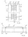
- FIG. 2is a perspective view of an embodiment of a wafer level package according to the invention, showing an insulating layer partially cut away to expose a redistribution layer.
- FIG. 3is a plan view of the wafer level package of FIG. 2 , without an insulating layer.
- FIG. 4is a cross-sectional, side elevational view of the wafer level package of FIG. 3 , taken along line 4 - 4 .
- FIG. 5is a plan view of another embodiment of a wafer level package according to the invention.
- FIG. 6is a partial view of the wafer level package of FIG. 3 , showing a portion of the redistribution layer.
- FIG. 7is a plan view of a processing step in the fabrication of the wafer level package of FIG. 2 , according to an embodiment of a method of the invention showing the bond pads exposed through openings in the insulating film.
- FIG. 8is a cross-sectional view of the package of FIG. 7 , taken along line 8 - 8 .
- FIG. 9is a partial cross-sectional view of the wafer level package of FIG. 4 , showing an embodiment of a multi-layered RDL.
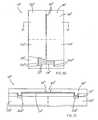
- FIG. 10is a plan view of a processing step in the fabrication of the wafer level package of FIG. 2 , in which an insulating layer, shown as partially cut away, is applied over the RDL layer, and ball contacts are mounted on the ball pads.
- FIG. 11is a cross-sectional view of the package of FIG. 10 , taken along line 11 - 11 .
- FIGS. 12-17illustrate sequential processing steps in the fabrication of another embodiment of a wafer level package according to the invention.
- FIG. 12is a plan view of a processing step in which an insulating layer, shown as partially cut away, is applied over the RDL of the package depicted in FIG. 3 , and openings are formed to the bond pads and ball pads.
- FIG. 13is a cross-sectional, side elevational view of the wafer level package of FIG. 12 , taken along line 13 - 13 .
- FIG. 14is a plan view of a subsequent processing step in which a second redistribution layer (RDL) is fabricated on the insulating layer, shown as partially cut away.
- RDLredistribution layer
- FIG. 15is a cross-sectional, side elevational view of the wafer level package of FIG. 14 , taken along line 15 - 15 .
- FIG. 16is a plan view of a subsequent processing step in which an insulating layer is applied over the second RDL of the package depicted in FIG. 14 , with ball contacts mounted on the ball pads of the dies.
- FIG. 17is a cross-sectional, side elevational view of the wafer level package of FIG. 16 , taken along line 17 - 17 .
- FIG. 18is a plan view of another embodiment of a wafer level package according to the invention, having a second redistribution layer disposed on a partially cut-away insulating layer overlying a first distribution layer.
- FIGS. 19-27illustrate sequential processing steps in the fabrication of another embodiment of a wafer level package according to the invention.
- FIG. 19is a plan view of a processing step in which a redistribution layer (RDL) is formed to connect bond pads of the dies of the package.
- RDLredistribution layer
- FIG. 20is a cross-sectional, side elevational view of the wafer level package of FIG. 19 , taken along line 20 - 20 .
- FIG. 21is a plan view of a subsequent processing step in which an insulating layer, shown as partially cut away, is applied over the RDL of the package depicted in FIG. 19 , and openings are formed to the bond pads of the dies.
- FIG. 22is a cross-sectional, side elevational view of the wafer level package of FIG. 21 , taken along line 22 - 22 .
- FIG. 23is a plan view of a subsequent processing step in which a second redistribution layer (RDL) is fabricated on the insulating layer, shown as partially cut away.
- RDLredistribution layer
- FIG. 24is a cross-sectional, side elevational view of the wafer level package of FIG. 23 , taken along line 24 - 24 .
- FIG. 25is a partial view of the package of FIG. 23 , showing a schematic depiction of trace connections of bond pads of the dies, with traces of the first RDL shown as broken lines.
- FIG. 26is a plan view of a subsequent processing step in which an insulating layer is applied over the second RDL of the package depicted in FIG. 24 , with ball contacts mounted on the ball pads of the dies.
- FIG. 27is a cross-sectional, side elevational view of the wafer level package of FIG. 26 , taken along line 27 - 27 .
- FIGS. 28-36illustrate sequential processing steps in the fabrication of another embodiment of a wafer level package according to the invention.
- FIG. 28is a plan view of a processing step in which a first redistribution layer (RDL) is formed to connect bond pads of the dies of the package.
- RDLredistribution layer
- FIG. 29is a cross-sectional, side elevational view of the wafer level package of FIG. 28 , taken along line 29 - 29 .
- FIG. 30is a plan view of a subsequent processing step in which a first insulating layer, shown as partially cut away, is applied over the first RDL of the package depicted in FIG. 28 , and openings are formed to the interconnecting traces.
- FIG. 31is a cross-sectional, side elevational view of the wafer level package of FIG. 30 , taken along line 31 - 31 .
- FIG. 32is a plan view of a subsequent processing step in which a second insulating layer, shown as partially cut away, is applied over the first insulating layer of the package depicted in FIG. 30 , with openings formed to the interconnecting traces, and a second redistribution layer (RDL) is fabricated on the second insulating layer to provide via interconnects to the interconnecting traces within the openings, and ball pads and traces connecting the via interconnects to the ball pads.
- RDLredistribution layer
- FIG. 33is a cross-sectional, side elevational view of the wafer level package of FIG. 32 , taken along line 33 - 33 .
- FIG. 34is a cross-sectional, side elevational view of the wafer level package of FIG. 32 , taken along line 34 - 34 .
- FIG. 35is a plan view of a subsequent processing step in which an insulating layer, shown as partially cut away, is applied over the second RDL of the package depicted in FIG. 32 , with openings formed to the ball pads, and ball contacts mounted on the ball pads of the dies.
- FIG. 36is a cross-sectional, side elevational view of the wafer level package of FIG. 35 , taken along line 36 - 36 .
- FIG. 37is a block diagram of a memory module incorporating a plurality of wafer level packages.
- the terms “semiconductive wafer fragment” or “wafer fragment” or “wafer”will be understood to mean any construction comprising semiconductor material, including but not limited to bulk semiconductive materials such as a semiconductor wafer (either alone or in assemblies comprising other materials thereon), and semiconductive material layers (either alone or in assemblies comprising other materials).
- substraterefers to any supporting structure including, but not limited to, the semiconductive wafer fragments or wafers described above.
- the present inventionprovides a semiconductor die package comprising two or more dies that can be fabricated at the wafer level, that is, an entire wafer of active device dies can be processed according to the invention to form one or more die packages, and burn-in and testing of the one or more packages can be performed before the wafer is separated into individual packages. It is also contemplated that packages can be defined as comprising, multiple, unseparated packages containing two or more dies, or whole or partial wafers.
- each package 10includes four dies 12 a - 12 d (delineated by the dashed lines), which is merely exemplary.
- the diesare fabricated on a surface of a substrate 14 , typically a semiconductor wafer, through etching, deposition, or other well known techniques, and contain integrated circuitry comprising active devices to perform a specific memory function.
- a dynamic random access memory circuitis exemplary of such an integrated circuit, although other circuits for any function, such as processors, can be packaged according to the invention.
- Scribe lines 16are typically provided between the wafer level packages 10 .
- the active surface 18 of the dies 12 a - 12 dincludes a series of bond pads 20 a - 20 d in electrical communication with the integrated circuits contained within each die 12 a - 12 d.
- the bond pads 20 a - 20 dare in a linear pattern in a longitudinal arrangement on each of the dies, although other bond pad arrangements can be utilized.
- a passivation or insulating (dielectric) film 22has been formed over the surface of the wafer 14 to passivate the active surface of the dies and to seal the device structures of the dies from contamination and moisture, and as a scratch protection layer. Openings formed in the insulating film align with and expose the bond 20 a - 20 d pads of the dies.
- the wafer level package 10further includes a redistribution layer (RDL) 24 formed on the insulating film 22 .
- the RDL 24includes electrically conductive traces 26 that connect the bond pads 20 a - 20 d of the dies to ball pads 28 for attaching external ball contacts 30 such as solder balls.
- the RDL 24 of the wafer level package 10also includes traces 32 that interconnect the bond pads of two or more of the dies within the wafer level package.
- the traces 32 of the RDLare formed to interconnect the bond pads 20 a of a first die 12 a to the bond pads 20 b of a second die 12 b, and the bond pads 20 c of a third die 12 c to the bond pads 20 d of a fourth die 12 d.
- the traces 32 ′ of the RDL 24 ′are patterned to interconnect the bond pads 20 a ′ of a first die 12 a ′ with the bond pads 20 c ′ of a third die 12 c ′, and the bond pads 20 b ′ of a second die 12 b ′ with the bond pads 20 d ′ of a fourth die 12 d ′.
- the illustrated trace interconnectionsare merely exemplary, and other configurations of the trace interconnections 32 can be utilized to interconnect the bond pads of the dies to each other and to the ball pads within the wafer level package.
- Each bond pad of a die within the wafer level packageis connected to a ball pad 28 either directly through a trace 26 , or indirectly through the interconnecting trace 32 leading to the bond pad of the adjoining die, which is then connected through the trace 26 to the ball pad 28 .
- the bond pad 20 b 1 of die 12 bis directly connected to the ball pad 28 ( b ) via the trace 26 .
- the bond pad 20 a 1 of die 12 ais also connected to the same ball pad 28 ( b ) indirectly through the interconnecting trace 32 and the trace 26 leading from the bond pad 20 b 1 of die 12 b.
- FIG. 7a processing step is illustrated in an embodiment of a method for forming the wafer level package 10 of FIG. 2 , which comprises four dies 12 a - 12 d.
- the semiconductor dies 12 a - 12 dare formed on a semiconductor wafer or other substrate 14 , through etching, deposition, or other well known techniques in the art, and respectively include bond pads 20 a - 20 d.
- the bond pads 20 a - 20 dtypically comprise a conductive metal or metal alloy such as aluminum, aluminum alloy, titanium, tungsten, titanium-tungsten alloy, tantalum, platinum, copper, or refractory metal silicide, for example, and are electrically connected to the die circuitry.
- an insulating film 22can be formed over the surface of the substrate 14 to passivate the active surface of the dies, as known in the art, typically by oxidizing or nitriding to form a silicon dioxide or silicon nitride layer or a combination of the two.
- the insulating film 22can also be formed of a dielectric material such as polyimide or another non-conductive elastomer, a photoimageable polymer such as benzocyclobutene (BCB), or a spin on glass (SOG) such as phosphosilicate glass (PSG), borosilicate glass (BSG) and borophosphosilicate glass (BPSG), among other insulating materials.
- the materialcan be applied using conventional methods including deposition techniques, spin coating, spraying, flow coating, brush coating, among other application techniques.
- the insulating film 22can be masked and etched by conventional methods to form openings 34 that align with and expose the bond pads 20 a - 20 d of the dies 12 a - 12 d.
- a redistribution layer (RDL) 24is formed on the insulating film 22 , which includes traces 26 , ball pads 28 , and interconnecting traces 32 .
- the present inventionutilizes a conductive redistribution wafer level package technology on two or more chips whereby, instead of the redistribution traces confined to a single chip (unit), the routing traces are extended to one or more adjacent chips (units) with all common signal buses being tied together.
- the structure of the redistribution layer to interconnect two or more dies within a packageincreases the memory capacity of the die package. For example, where redistribution traces interconnect two die units, the memory capacity of the combined units is double. This capacity can be extended to additional multiple units, for example, four units, eight units, sixteen units, and so on.
- the present inventionthus results in an increase in the capacity of a singulated unit or die package as a wafer scale (level) package. Further, since address, data and some control buses or even power/ground pins for memory devices are shared, the number of pin-out/contact balls for the integrated package is reduced compared to single die units.
- the RDL 24typically comprises a highly conductive metal or metal alloy such as copper, aluminum, gold, and nickel, for example, or a conductive polymer material.
- the RDL 24can be formed using known techniques in the art such as chemical vapor deposition (CVD), plasma enhanced chemical vapor deposition (PECVD), physical vapor deposition (PVD) (sputtering or evaporation), electroplating, electroless plating, stenciling, and screen printing, for example.
- the RDL 24can comprise, for example, a foil tape of copper, aluminum or other suitable metal, that can be stamp-cut to provide the desired pattern of traces and ball pads.
- the RDLcan also comprise a multiple metal layers applied over the insulating film 22 according to known techniques, to form a sandwich or multi-layer under-bump metallurgy (UBM) structure, typically having a tri-metal layer structure.
- the multiple metal layer RDL 24can comprise overlying layers 36 a - 36 c of a conductive material such as overlying layers of aluminum, nickel, and copper, or overlying layers of chromium, chromium/copper, and copper, for example.
- the third metal layer 36 cis extended to route traces over adjacent units.
- an insulating layer 38is then applied over the RDL 24 to form a passive exterior layer over the traces 26 , 32 .
- the insulating layer 38can comprise, for example, a polymeric material such as polyimide or another non-conductive elastomer, or a photoimageable polymer such as benzocyclobutene (BCB).
- the materialcan be applied using conventional methods, and the insulating layer 38 can be patterned and etched according to known techniques to provide openings 40 that align with and expose the ball pads 28 .
- a plurality of ball contacts 30are attached to the ball pads 28 for connecting the wafer level package 10 as a component to an external circuit board, motherboard or other electrical apparatus or device.
- Exemplary ball contacts 30comprise solder typically comprising tin (Sn) and/or lead (Pb), or a conductive material such as a conductive epoxy or conductor-filled epoxy.
- Solder ball contacts 30can be formed using conventional processes such as stenciling, screen printing, electroplating, electroless plating, evaporation, and the like. Conductive polymer material can be applied and cured to form the ball contacts.
- the wafercan then singulated along scribe lines 16 into individual packages 10 , each of which include at least two dies, and shown as four interconnected dies 12 a - 12 d in the illustrated example.
- the packagecan be fabricated with one or more overlying RDLs to interconnect additional dies within a package, as depicted in FIGS. 12-17 .
- an initial RDL layer 24 ′′comprising traces 32 ′′ interconnecting the bond pads 20 a ′′ to 20 b ′′ of the first and second dies 12 a ′′, 12 b ′′, and the bond pads 20 c ′′ to 20 d ′′ of the third and fourth dies 12 c ′′, 12 d ′′ can be fabricated as described with respect to the wafer level package 10 of FIG. 3 . As illustrated in FIGS.
- openings 34 ′′, 46 ′′are formed through the insulating layer 38 ′′, respectively to align with and expose the bond pads 20 a ′′- 20 d ′′ and ball pads 28 ′′ of the initial RDL 24 ′′.
- a second RDL 44 ′′can then be applied onto the insulating layer 38 ′′, with traces 48 ′′ interconnecting the bond pads 20 a ′′ to 20 c ′′ of the first and third dies 12 a ′′, 12 c ′′, and the bond pads 20 b ′′ to 20 d ′′ of the second and fourth dies 12 b ′′, 12 d ′′, for example.
- all dies 12 a ′′- 12 d ′′ of the wafer level package 10 ′′are interconnected by means of the interconnecting traces 32 ′′, 48 ′′ of the first and second RDLs 24 ′′, 44 ′′.
- an insulating layer 50 ′′can then be applied over the RDL 44 ′′ to form a passive exterior layer, with openings provided to the balls pads 28 ′′, and ball contacts 30 ′′ can be connected to the ball pads 28 ′′.
- FIG. 18Another example of a configuration of a second RDL 44 ′′ is illustrated in FIG. 18 .
- the initial RDL 24 ′′′is configured similar to the RDL 24 shown in FIG. 3 .
- the second RDL 44 ′′′has been fabricated on the insulating layer 38 ′′′ such that the traces 32 ′′′ interconnect the bond pads 12 a ′′′ to the bond pads 12 d ′′′ of the first and fourth dies 12 a ′′′, 12 d ′′′, resulting in the interconnection of all four dies 12 a ′′′- 12 d ′′′ within the package 10 ′′′.
- Other configurations of two or more RDLscan be utilized to interconnect two or more dies within a wafer level package.
- the packagecan comprise two or more redistribution layers (RDLs) whereby the ball pads are fabricated as part of the second (or subsequent) RDL.
- RDLsredistribution layers
- a first RDL 24 ′′′′is fabricated on a insulating film 28 ′′′′.
- the RDL 24 ′′′′comprises traces 32 ′′′′ interconnecting the bond pads 20 a ′′′′ to 20 b ′′′′ of the first and second dies 12 a ′′′′, 12 b ′′′′, and the bond pads 20 c ′′′′ to 20 d ′′′′ of the third and fourth dies 12 c ′′′′, 12 d ′′′′.
- An insulating layer 38 ′′′′can be applied over the RDL 24 ′′′′, and openings 34 ′′′′ formed through the layer to align with and expose the bond pads 20 a ′′′′- 20 d ′′′′, as illustrated in FIG. 21-22 .
- a second RDL 44 ′′′′can then be formed on the insulating layer 38 ′′′′.
- the RDL 44 ′′′′can comprise traces 48 ′′′′ interconnecting the bond pads of two dies in the packages, illustrated as connecting bond pads 20 b ′′′′ to 20 c ′′′′ of the second and third dies 12 b ′′′′, 12 c ′′′′, for example.
- Other trace connections 48 ′′′′can be provided as illustrated, for example, in FIGS. 14 and 18 .
- RDL 44 ′′′′further comprises ball pads 56 ′′′′ that are connected through traces 58 ′′′′ to bond pads 20 a ′′′′- 20 d ′′′′ of the dies.
- each bond pad of a diecommunicates with a ball pad 56 ′′′′ either directly through a trace 58 ′′′′, or indirectly through the interconnecting trace 32 ′′′′ and/or 48 ′′′′ leading to the bond pad of the adjoining die, which is then connected through the trace 58 ′′′′ to the ball pad 56 ′′′′.
- trace 58 ′′′′directly connects bond pad 20 b ′′′′ to the ball pad 56 ′′′′; and traces 32 ′′′′, 48 ′′′′ and/or 58 ′′′′ indirectly connect bonds pads 20 a ′′′′, 20 c ′′′′, and 20 d ′′′′ to the same ball pad 56 ′′′′.
- dies 12 a ′′′′- 12 d ′′′′ of package 10 ′′′′being interconnected to the same ball pad 56 ′′′′.
- an insulating layer 50 ′′′′can then be applied over the RDL 44 ′′′′ to form a passive exterior layer, with openings to the ball pads 56 ′′′′.
- Ball contacts 30 ′′′′can then be connected to the ball pads 56 ′′′′.
- FIGS. 28-36Another embodiment of a wafer level package 10 v according to the invention is depicted in FIGS. 28-36 .
- initial RDL layer 24 vis fabricated on an insulating film 22 v disposed over the dies on the wafer surface, and includes traces 32 v interconnecting the bond pads 20 a v to 20 b v of the first and second dies 12 a v , 12 b v , and the bond pads 20 c v to 20 d v of the third and fourth dies 12 c v , 12 d v .
- FIGS. 28-29shows that initial RDL layer 24 v is fabricated on an insulating film 22 v disposed over the dies on the wafer surface, and includes traces 32 v interconnecting the bond pads 20 a v to 20 b v of the first and second dies 12 a v , 12 b v , and the bond pads 20 c v to 20 d v of the third and
- an insulating layer 38 vis then applied over the RDL 24 v to form a passive layer over the interconnecting traces 32 v , with openings 60 v formed between adjoining dies 12 a v , 12 b v and 12 c v , 12 d v to expose the interconnecting traces 32 v .
- a second insulating layer 62 vis formed over the insulating layer 38 v as depicted in FIGS. 32-33 , and is patterned and etched to provide openings 64 v and to extend opening 60 v .
- a second RDL 44 vis then applied onto the insulating layer 62 v to form via interconnects 66 v within opening 60 v connected to interconnecting traces 32 v , ball pads 68 v , and traces 70 v that interconnect the ball pads 68 v to every other via interconnect 66 v in a staggered arrangement. As depicted in FIGS.
- an insulating layer 50 vcan then be applied over the second RDL 44 v to form a passive exterior layer, with openings 72 v to the ball pads 68 v .
- Ball contacts 30 vcan then be connected to the ball pads 68 v .
- This arrangement of vias 66 v and trace connections 70 v of vias 66 v to the ball pads 68 vprovides closely matched RDL lengths from the bond pads 20 a v , 20 b v to the ball pads 68 v .
- the inactive surface 52 of the wafer level package 10can be covered with a protective dielectric layer 54 such as a photoresist or spun-on polyimide, for example, which can be applied after backgrinding of the wafer or other substrate 14 , and prior to singulation.
- a protective dielectric layer 54such as a photoresist or spun-on polyimide, for example, which can be applied after backgrinding of the wafer or other substrate 14 , and prior to singulation.
- the electrical testing and burn-in of the diesis performed before the substrate (wafer) 14 is singulated into individual packages 10 .
- the packaged dies 10can be severed from the substrate (wafer) 14 singularly or in groups as desired. It is also contemplated that an entire unsevered wafer 14 can be tested and burned-in, and then used as fabricated as a wafer-scale package, particularly for large-capacity memory applications.
- the finished wafer level package 10can be mounted as a component on an end user's printed
- a circuit modulecan comprise a combination of dies representing a variety of functions or containing the same functionality.
- integrated circuit modulesinclude memory modules, device drivers, power modules, communication modems, processor modules and application-specific modules and may include multilayer, multi-chip modules.
- multi-chip modulesinclude a single in-line memory module (SIMM), a dual in-line memory module (DIMM), a random access memory (RAM) card or module, and a read-only-memory (ROM) card or module.
- the circuit modulecan be a subcomponent of a variety of electronic systems, for example, a personal computer, cellular phone, clock, television, automobile, industrial control system, among others.
- FIG. 37schematically depicts an embodiment of an integrated circuit module as a multi-chip memory module 74 , such as a SIMM or DIMM, which are generally a printed circuit board (PCB) or other support containing a series of memory devices, or a memory card or any other memory die-carrying substrate.
- a SIMMtypically comprises a single inline set of contacts or leads
- a DIMMtypically comprises a set of leads on each side of the support with each set representing separate I/O signals.
- the memory module 74comprises multiple wafer level packages 10 disposed on a support 76 , the number of packages 10 depending upon the desired bus width and the desire for parity. Wafer level packages 10 can be disposed on both sides of the support 76 .
- the memory module 74accepts a command signal from an external controller (not shown) on a command link 78 and provides for data input and data output on data links 80 , both of which are connected to leads 82 extending from the support 76 .
Landscapes
- Engineering & Computer Science (AREA)
- Microelectronics & Electronic Packaging (AREA)
- Power Engineering (AREA)
- Computer Hardware Design (AREA)
- Physics & Mathematics (AREA)
- Condensed Matter Physics & Semiconductors (AREA)
- General Physics & Mathematics (AREA)
- Internal Circuitry In Semiconductor Integrated Circuit Devices (AREA)
- Production Of Multi-Layered Print Wiring Board (AREA)
- Semiconductor Integrated Circuits (AREA)
Abstract
Description
- This application is a divisional of U.S. patent application Ser. No. 10/167,284, filed Jun. 11, 2002, which claims priority to Singapore Patent Application No. 200203050-0, filed May 21, 2002.
- This invention relates generally to integrated circuit chip packages, and more specifically to a method of forming an integrated circuit package at a wafer level.
- With the increase in memory needed by software, the trend in state-of-the-art microprocessors is toward higher performance, high-density memory modules, such as single in-line memory modules (SIMMs) or dual in-line memory modules (DIMMs), which are circuit cards with memory chips attached. Having higher capacity memory chip units or packing more memory chip units on a memory module is one way to increase memory density on a module.
- Conventional methods of mounting multiple die units on a module is through stacking the die units or attaching a daughter board to the main module board. However, a profusion of small electronic products such as pages and cellular telephones demand small product size and low profile products. The demand by consumers for miniature electronic devices has increased the need for powerful yet compact, ultra-thin semiconductor devices.
- Based on these and other needs and deficiencies, an improved die package for achieving a high density memory module would be desirable.
- The present invention provides a wafer level semiconductor die package, a semiconductor wafer comprising one or more wafer level packages, an electronic system comprising an integrated circuit module that includes one or more of the wafer level packages, a memory module comprising a printed circuit board and an integrated circuit module that includes at least one of the wafer level packages, and methods of fabricating the die packages on a wafer level, and integrated circuit modules that include one or more packages.
- In one aspect, the invention provides a die package. In one embodiment, the die package comprises a redistribution layer interconnecting two or more dies disposed on a substrate, typically a semiconductor wafer, the redistribution layer comprising a first trace connecting a bond pad of each of two dies, and a second trace connecting one of the bond pads of the two dies to a ball pad. The die package can further include an insulating layer disposed over the traces, and/or a ball contact mounted on the ball pad.
- In another embodiment, the die package is an integrated wafer level package comprising a plurality of electrically conductive traces disposed on an insulating film overlying two or more dies disposed on a semiconductor wafer or other substrate, each die comprising one or more bond pads, and each of the bond pads exposed through an opening in the insulating film; a redistribution layer comprising a plurality of traces and ball pads disposed on the insulating film, and a first trace of the redistribution layer interconnecting a bond pad of a first die to the bond pad of a second die, and a second trace connecting one of said bond pads to a ball pad disposed on the insulating film. Thus, a trace connects each bond pad of the dies to either a ball pad or to the bond pad of another die which bond pad is connected by a trace to a ball pad.
- In another embodiment, the die package comprises an integrated wafer level package, comprising a support substrate, typically a semiconductor wafer, comprising at least three semiconductor dies, each die comprising a plurality of bond pads; an insulating film disposed over the dies with openings exposing the bond pads of the dies; a plurality of traces and ball pads disposed on the insulating film; a bond pad of each of a first die and second die interconnected by a trace, and one of said bond pads of the first and second dies connected by a trace to a ball pad; an insulating layer disposed over the traces; and a plurality of traces disposed on the insulating layer, including a trace connecting a bond pad of either the first die or the second die to a bond pad of a third die.
- In yet another embodiment, the die package comprises an integrated wafer level package, comprising a semiconductor wafer or other support substrate comprising three or more semiconductor dies, each die comprising one or more bond pads, and a first redistribution layer including a trace interconnecting a bond pad of each of a first die and a second die; an insulating layer disposed over the first redistribution layer and comprising openings exposing the bond pads of the dies; and a second redistribution layer comprising a plurality of traces disposed on the insulating layer;, including a trace interconnecting a bond pad of either the first die or the second die to a bond pad of a third die; wherein one of the bond pads of the first, second or third dies is connected by a trace to a ball pad within the package. The first redistribution layer can be disposed on an insulating film overlying the dies. The ball pad can be part of the first redistribution layer and connected by a trace to one of the bond pads of the first and second dies, or part of the second redistribution layer with a trace of the second redistribution layer connecting the bond pad of any of the first, second or third dies to the ball pad.
- In yet another embodiment, the die package comprises an integrated wafer level package, comprising a semiconductor wafer or other support substrate comprising two or more dies, each die comprising a plurality of bond pads; an insulating film disposed over the dies, the film comprising openings aligned with and exposing the bond pads of the dies; a first redistribution layer disposed on the insulating film and including a trace interconnecting a bond pad of each of a first die and a second die; a first insulating layer disposed over the first redistribution layer and comprising openings exposing at least one of the first traces; a second insulating layer disposed over the first insulating layer and comprising openings exposing the first trace(s) and openings for ball pads; and a second redistribution layer comprising a ball pad and a trace disposed on the second insulating layer, and a via interconnect disposed in the opening onto the first trace, the second trace connecting the via interconnect to the ball pad.
- In another aspect, the invention provides a semiconductor wafer. In various embodiments, the wafer comprises one or more wafer level packages according to the invention.
- In another aspect, the invention provides an electronic system comprising an integrated circuit module comprising at least one wafer level package according to the invention. In one embodiment the integrated circuit module comprises a multi-chip module, such as a DIMM board, among others.
- In yet another aspect, the invention provides a memory module comprising a printed circuit board and an integrated circuit module comprising at least one wafer level package according to the invention. In one embodiment, the memory module can comprise an integrated circuit module in the form of a DIMM board or other multi-chip module.
- In a further aspect, the invention provides methods of fabricating the foregoing die packages on a wafer level. In an embodiment of a method of fabricating a die package on a wafer level, the method comprises forming a redistribution layer over at least two dies disposed on a semiconductor wafer or other support substrate, the redistribution layer comprising a plurality of traces and one or more ball pads including a trace connecting a bond pad of each of a first and second die, and a trace connecting one of the bond pads to a ball pad.
- In another embodiment of a method of fabricating a wafer level die package, the method comprises providing a substrate having a plurality of semiconductor dies formed thereon, each die comprising one or more bond pads; applying an insulating film over the substrate; forming openings through the insulating film to the bond pads of the dies; and forming a redistribution layer over the insulating film, the redistribution layer comprising a plurality of traces and ball pads, including a trace interconnecting a bond pad of each of a first die and a second die, and a trace connecting one of the bond pads of the first and second dies to a ball pad. The method can further include steps of applying an insulating layer over the redistribution layer and forming openings through the insulating layer to the ball pads, and mounting a ball contact on each of the ball pads. In another embodiment, the insulating layer can be applied over the redistribution layer and openings formed to the bond pads and ball pads, and a second redistribution comprising a plurality of traces can be formed over the insulating layer, including a trace interconnecting a bond pad of either the first die or the second die to a bond pad of a third die.
- In yet another embodiment of a method of fabricating a die package on a wafer level, the method comprises forming a first redistribution layer over a plurality of dies disposed on a semiconductor wafer or other substrate, including a trace interconnecting a bond pad of each of a first die and a second die; applying an insulating layer over the traces which includes openings to the bond pads of the dies; and forming a second redistribution layer comprising a plurality of traces and ball pads over the insulating layer, including a trace interconnecting a bond pad of either the first or the second die to a bond pad of a third die; wherein a trace of either the first or second redistribution layers connects one of said bond pads of the first, second or third dies to a ball pad. The ball pad can be provided as part of the first redistribution layer formed on an insulating film overlying the dies whereby the ball pad is connected by a trace to one of the interconnected bond pads of the first or second dies. In another embodiment, the ball pad can be provided as part of the second redistribution layer, connected by a trace to one of the interconnected bond pads of the first, second or third dies.
- In yet another embodiment of a method of fabricating a die package on a wafer level, the method comprises forming a first redistribution layer over at least two dies disposed on a substrate, the first redistribution layer comprising a plurality of traces including a trace connecting a bond pad of each of the two dies; forming an insulating layer over the first redistribution layer; forming openings through the insulating layer to expose each of the traces of the first redistribution layer; and forming a second redistribution layer over the insulating layer, the second redistribution layer comprising a plurality of ball pads and traces, and a via interconnect disposed in each of the openings of the insulating layer in contact with the trace of the first RDL, the trace of the second RDL connecting the via interconnect to at least one ball pad. The method can further comprise the steps of forming an insulating layer over the second redistribution layer; forming openings to expose the ball pads; and connecting ball contacts to the ball pads of the second redistribution layer; and further singulating the wafer to form individual packages, each package comprising the first and second dies connected by the traces of the first redistribution layer.
- In another aspect, the invention provides methods for fabricating an integrated circuit module. In one embodiment, the method comprises the steps of providing a substrate comprising a plurality of wafer level packages according to the invention; separating each package on the substrate to form individual packages; and assembling one or more packages into an integrated circuit module, for example, a multi-chip module such as a DIMM board.
- The present invention provides a multiple die package having an exceptionally high memory capacity with a low profile. The die package achieves a single unit (die package) having an increased memory capacity using current memory chips by virtue the interconnections between two or more chips within the package, without having to wait for the availability of the next higher density chip. The integrated wafer package also has the advantage of space saving on a module board due to the compact and thin profile, which in turn allows more integrated units/packages and higher memory capacity on the flip chip memory module such as a SIMM or DIMM board. The die package also provides superior signal integrity.
- The configuration of the RDL with traces connecting bond pads of two or more dies together and routing the connection to a single ball pad also eliminates the need for a separate pin or ball contact for each individual bond pad, resulting in a lower pin count compared to other memory module chip units. The package also is easier to lay out on a DIMM board or or other memory module since part of the routing is done on a wafer level.
- Preferred embodiments of the invention are described below with reference to the following accompanying drawings, which are for illustrative purposes only. Throughout the following views, the reference numerals will be used in the drawings, and the same reference numerals will be used throughout the several views and in the description to indicate same or like parts.
FIG. 1 is a plan view of a substrate containing wafer level packages according to the invention.FIG. 2 is a perspective view of an embodiment of a wafer level package according to the invention, showing an insulating layer partially cut away to expose a redistribution layer.FIG. 3 is a plan view of the wafer level package ofFIG. 2 , without an insulating layer.FIG. 4 is a cross-sectional, side elevational view of the wafer level package ofFIG. 3 , taken along line4-4.FIG. 5 is a plan view of another embodiment of a wafer level package according to the invention.FIG. 6 is a partial view of the wafer level package ofFIG. 3 , showing a portion of the redistribution layer.FIG. 7 is a plan view of a processing step in the fabrication of the wafer level package ofFIG. 2 , according to an embodiment of a method of the invention showing the bond pads exposed through openings in the insulating film.FIG. 8 is a cross-sectional view of the package ofFIG. 7 , taken along line8-8.FIG. 9 is a partial cross-sectional view of the wafer level package ofFIG. 4 , showing an embodiment of a multi-layered RDL.FIG. 10 is a plan view of a processing step in the fabrication of the wafer level package ofFIG. 2 , in which an insulating layer, shown as partially cut away, is applied over the RDL layer, and ball contacts are mounted on the ball pads.FIG. 11 is a cross-sectional view of the package ofFIG. 10 , taken along line11-11.FIGS. 12-17 illustrate sequential processing steps in the fabrication of another embodiment of a wafer level package according to the invention.- FIG.12 is a plan view of a processing step in which an insulating layer, shown as partially cut away, is applied over the RDL of the package depicted in
FIG. 3 , and openings are formed to the bond pads and ball pads. FIG. 13 is a cross-sectional, side elevational view of the wafer level package ofFIG. 12 , taken along line13-13.FIG. 14 is a plan view of a subsequent processing step in which a second redistribution layer (RDL) is fabricated on the insulating layer, shown as partially cut away.FIG. 15 is a cross-sectional, side elevational view of the wafer level package ofFIG. 14 , taken along line15-15.FIG. 16 is a plan view of a subsequent processing step in which an insulating layer is applied over the second RDL of the package depicted inFIG. 14 , with ball contacts mounted on the ball pads of the dies.FIG. 17 is a cross-sectional, side elevational view of the wafer level package ofFIG. 16 , taken along line17-17.FIG. 18 is a plan view of another embodiment of a wafer level package according to the invention, having a second redistribution layer disposed on a partially cut-away insulating layer overlying a first distribution layer.FIGS. 19-27 illustrate sequential processing steps in the fabrication of another embodiment of a wafer level package according to the invention.FIG. 19 is a plan view of a processing step in which a redistribution layer (RDL) is formed to connect bond pads of the dies of the package.FIG. 20 is a cross-sectional, side elevational view of the wafer level package ofFIG. 19 , taken along line20-20.FIG. 21 is a plan view of a subsequent processing step in which an insulating layer, shown as partially cut away, is applied over the RDL of the package depicted inFIG. 19 , and openings are formed to the bond pads of the dies.FIG. 22 is a cross-sectional, side elevational view of the wafer level package ofFIG. 21 , taken along line22-22.FIG. 23 is a plan view of a subsequent processing step in which a second redistribution layer (RDL) is fabricated on the insulating layer, shown as partially cut away.FIG. 24 is a cross-sectional, side elevational view of the wafer level package ofFIG. 23 , taken along line24-24.FIG. 25 is a partial view of the package ofFIG. 23 , showing a schematic depiction of trace connections of bond pads of the dies, with traces of the first RDL shown as broken lines.FIG. 26 is a plan view of a subsequent processing step in which an insulating layer is applied over the second RDL of the package depicted inFIG. 24 , with ball contacts mounted on the ball pads of the dies.FIG. 27 is a cross-sectional, side elevational view of the wafer level package ofFIG. 26 , taken along line27-27.FIGS. 28-36 illustrate sequential processing steps in the fabrication of another embodiment of a wafer level package according to the invention.FIG. 28 is a plan view of a processing step in which a first redistribution layer (RDL) is formed to connect bond pads of the dies of the package.FIG. 29 is a cross-sectional, side elevational view of the wafer level package ofFIG. 28 , taken along line29-29.FIG. 30 is a plan view of a subsequent processing step in which a first insulating layer, shown as partially cut away, is applied over the first RDL of the package depicted inFIG. 28 , and openings are formed to the interconnecting traces.FIG. 31 is a cross-sectional, side elevational view of the wafer level package ofFIG. 30 , taken along line31-31.FIG. 32 is a plan view of a subsequent processing step in which a second insulating layer, shown as partially cut away, is applied over the first insulating layer of the package depicted inFIG. 30 , with openings formed to the interconnecting traces, and a second redistribution layer (RDL) is fabricated on the second insulating layer to provide via interconnects to the interconnecting traces within the openings, and ball pads and traces connecting the via interconnects to the ball pads.FIG. 33 is a cross-sectional, side elevational view of the wafer level package ofFIG. 32 , taken along line33-33.FIG. 34 is a cross-sectional, side elevational view of the wafer level package ofFIG. 32 , taken along line34-34.FIG. 35 is a plan view of a subsequent processing step in which an insulating layer, shown as partially cut away, is applied over the second RDL of the package depicted inFIG. 32 , with openings formed to the ball pads, and ball contacts mounted on the ball pads of the dies.FIG. 36 is a cross-sectional, side elevational view of the wafer level package ofFIG. 35 , taken along line36-36.FIG. 37 is a block diagram of a memory module incorporating a plurality of wafer level packages.- The invention will be described generally with reference to the drawings for the purpose of illustrating embodiments only and not for purposes of limiting the same. The figures illustrate processing steps for use in fabricating semiconductor devices in accordance with the present invention. It should be readily apparent that the processing steps are only a portion of the entire fabrication process.
- In the current application, the terms “semiconductive wafer fragment” or “wafer fragment” or “wafer” will be understood to mean any construction comprising semiconductor material, including but not limited to bulk semiconductive materials such as a semiconductor wafer (either alone or in assemblies comprising other materials thereon), and semiconductive material layers (either alone or in assemblies comprising other materials). The term “substrate” refers to any supporting structure including, but not limited to, the semiconductive wafer fragments or wafers described above.
- The present invention provides a semiconductor die package comprising two or more dies that can be fabricated at the wafer level, that is, an entire wafer of active device dies can be processed according to the invention to form one or more die packages, and burn-in and testing of the one or more packages can be performed before the wafer is separated into individual packages. It is also contemplated that packages can be defined as comprising, multiple, unseparated packages containing two or more dies, or whole or partial wafers.
- Referring to
FIGS. 1-4 , a first embodiment of an integratedwafer level package 10 according to the invention is depicted. Thewafer level package 10 comprises two or more semiconductor dies. For illustrative purposes, eachpackage 10 includes four dies12a-12d(delineated by the dashed lines), which is merely exemplary. - The dies are fabricated on a surface of a
substrate 14, typically a semiconductor wafer, through etching, deposition, or other well known techniques, and contain integrated circuitry comprising active devices to perform a specific memory function. A dynamic random access memory circuit is exemplary of such an integrated circuit, although other circuits for any function, such as processors, can be packaged according to the invention. Scribe lines16 are typically provided between the wafer level packages10. Theactive surface 18 of the dies12a-12dincludes a series ofbond pads 20a-20din electrical communication with the integrated circuits contained within each die12a-12d.In the illustrated example, thebond pads 20a-20dare in a linear pattern in a longitudinal arrangement on each of the dies, although other bond pad arrangements can be utilized. A passivation or insulating (dielectric)film 22 has been formed over the surface of thewafer 14 to passivate the active surface of the dies and to seal the device structures of the dies from contamination and moisture, and as a scratch protection layer. Openings formed in the insulating film align with and expose thebond 20a-20dpads of the dies. - The
wafer level package 10 further includes a redistribution layer (RDL)24 formed on the insulatingfilm 22. TheRDL 24 includes electricallyconductive traces 26 that connect thebond pads 20a-20dof the dies toball pads 28 for attachingexternal ball contacts 30 such as solder balls. - According to the invention, the
RDL 24 of thewafer level package 10 also includestraces 32 that interconnect the bond pads of two or more of the dies within the wafer level package. For example, as illustrated inFIG. 3 , in the embodiment of thewafer level package 10, thetraces 32 of the RDL are formed to interconnect thebond pads 20aof afirst die 12ato thebond pads 20bof asecond die 12b,and thebond pads 20cof athird die 12cto thebond pads 20dof afourth die 12d.Referring toFIG. 5 , in another embodiment of awafer level package 10′ according to the invention, thetraces 32′ of theRDL 24′ are patterned to interconnect thebond pads 20a′ of afirst die 12a′ with thebond pads 20c′ of athird die 12c′, and thebond pads 20b′ of asecond die 12b′ with thebond pads 20d′ of afourth die 12d′. The illustrated trace interconnections are merely exemplary, and other configurations of thetrace interconnections 32 can be utilized to interconnect the bond pads of the dies to each other and to the ball pads within the wafer level package. - Each bond pad of a die within the wafer level package is connected to a
ball pad 28 either directly through atrace 26, or indirectly through the interconnectingtrace 32 leading to the bond pad of the adjoining die, which is then connected through thetrace 26 to theball pad 28. For example, referring toFIG. 6 , thebond pad 20b1ofdie 12bis directly connected to the ball pad28(b) via thetrace 26. As further shown, thebond pad 20a1ofdie 12ais also connected to the same ball pad28(b) indirectly through the interconnectingtrace 32 and thetrace 26 leading from thebond pad 20b1ofdie 12b. - Referring now to
FIG. 7 , a processing step is illustrated in an embodiment of a method for forming thewafer level package 10 ofFIG. 2 , which comprises four dies12a-12d.The semiconductor dies12a-12dare formed on a semiconductor wafer orother substrate 14, through etching, deposition, or other well known techniques in the art, and respectively includebond pads 20a-20d.Thebond pads 20a-20dtypically comprise a conductive metal or metal alloy such as aluminum, aluminum alloy, titanium, tungsten, titanium-tungsten alloy, tantalum, platinum, copper, or refractory metal silicide, for example, and are electrically connected to the die circuitry. - As also shown in
FIG. 8 , an insulatingfilm 22 can be formed over the surface of thesubstrate 14 to passivate the active surface of the dies, as known in the art, typically by oxidizing or nitriding to form a silicon dioxide or silicon nitride layer or a combination of the two. The insulatingfilm 22 can also be formed of a dielectric material such as polyimide or another non-conductive elastomer, a photoimageable polymer such as benzocyclobutene (BCB), or a spin on glass (SOG) such as phosphosilicate glass (PSG), borosilicate glass (BSG) and borophosphosilicate glass (BPSG), among other insulating materials. The material can be applied using conventional methods including deposition techniques, spin coating, spraying, flow coating, brush coating, among other application techniques. The insulatingfilm 22 can be masked and etched by conventional methods to formopenings 34 that align with and expose thebond pads 20a-20dof the dies12a-12d. - As illustrated in
FIGS. 3-4 , a redistribution layer (RDL)24 is formed on the insulatingfilm 22, which includes traces26,ball pads 28, and interconnecting traces32. - The present invention utilizes a conductive redistribution wafer level package technology on two or more chips whereby, instead of the redistribution traces confined to a single chip (unit), the routing traces are extended to one or more adjacent chips (units) with all common signal buses being tied together. The structure of the redistribution layer to interconnect two or more dies within a package increases the memory capacity of the die package. For example, where redistribution traces interconnect two die units, the memory capacity of the combined units is double. This capacity can be extended to additional multiple units, for example, four units, eight units, sixteen units, and so on. The present invention thus results in an increase in the capacity of a singulated unit or die package as a wafer scale (level) package. Further, since address, data and some control buses or even power/ground pins for memory devices are shared, the number of pin-out/contact balls for the integrated package is reduced compared to single die units.
- The
RDL 24 typically comprises a highly conductive metal or metal alloy such as copper, aluminum, gold, and nickel, for example, or a conductive polymer material. TheRDL 24 can be formed using known techniques in the art such as chemical vapor deposition (CVD), plasma enhanced chemical vapor deposition (PECVD), physical vapor deposition (PVD) (sputtering or evaporation), electroplating, electroless plating, stenciling, and screen printing, for example. TheRDL 24 can comprise, for example, a foil tape of copper, aluminum or other suitable metal, that can be stamp-cut to provide the desired pattern of traces and ball pads. - The RDL can also comprise a multiple metal layers applied over the insulating
film 22 according to known techniques, to form a sandwich or multi-layer under-bump metallurgy (UBM) structure, typically having a tri-metal layer structure. As depicted inFIG. 9 , for example, the multiplemetal layer RDL 24 can compriseoverlying layers 36a-36cof a conductive material such as overlying layers of aluminum, nickel, and copper, or overlying layers of chromium, chromium/copper, and copper, for example. Ideally, in utilizing a tri-metal layer structure, thethird metal layer 36cis extended to route traces over adjacent units. - As shown in
FIGS. 10-11 , an insulatinglayer 38 is then applied over theRDL 24 to form a passive exterior layer over thetraces layer 38 can comprise, for example, a polymeric material such as polyimide or another non-conductive elastomer, or a photoimageable polymer such as benzocyclobutene (BCB). The material can be applied using conventional methods, and the insulatinglayer 38 can be patterned and etched according to known techniques to provideopenings 40 that align with and expose theball pads 28. - A plurality of
ball contacts 30 are attached to theball pads 28 for connecting thewafer level package 10 as a component to an external circuit board, motherboard or other electrical apparatus or device.Exemplary ball contacts 30 comprise solder typically comprising tin (Sn) and/or lead (Pb), or a conductive material such as a conductive epoxy or conductor-filled epoxy.Solder ball contacts 30 can be formed using conventional processes such as stenciling, screen printing, electroplating, electroless plating, evaporation, and the like. Conductive polymer material can be applied and cured to form the ball contacts. - The wafer can then singulated along
scribe lines 16 intoindividual packages 10, each of which include at least two dies, and shown as four interconnected dies12a-12din the illustrated example. - In another embodiment of a
wafer level package 10″ according to the invention, the package can be fabricated with one or more overlying RDLs to interconnect additional dies within a package, as depicted inFIGS. 12-17 . By way of example, aninitial RDL layer 24″ comprising traces32″ interconnecting thebond pads 20a″ to20b″ of the first and second dies12a″,12b″, and thebond pads 20c″ to20d″ of the third and fourth dies12c″,12d″ can be fabricated as described with respect to thewafer level package 10 ofFIG. 3 . As illustrated inFIGS. 12-13 ,openings 34″,46″ are formed through the insulatinglayer 38″, respectively to align with and expose thebond pads 20a″-20d″ andball pads 28″ of theinitial RDL 24″. As depicted inFIGS. 14-15 , asecond RDL 44″ can then be applied onto the insulatinglayer 38″, withtraces 48″ interconnecting thebond pads 20a″ to20c″ of the first and third dies12a″,12c″, and thebond pads 20b″ to20d″ of the second and fourth dies12b″,12d″, for example. Thus, all dies12a″-12d″ of thewafer level package 10″ are interconnected by means of the interconnecting traces32″,48″ of the first andsecond RDLs 24″,44″. As depicted inFIGS. 16-17 , an insulatinglayer 50″ can then be applied over theRDL 44″ to form a passive exterior layer, with openings provided to theballs pads 28″, andball contacts 30″ can be connected to theball pads 28″. - Another example of a configuration of a
second RDL 44″ is illustrated inFIG. 18 . In the illustrated embodiment of awafer level package 10′″, theinitial RDL 24′″ is configured similar to theRDL 24 shown inFIG. 3 . Thesecond RDL 44′″ has been fabricated on the insulatinglayer 38′″ such that thetraces 32′″ interconnect thebond pads 12a′″ to thebond pads 12d′″ of the first and fourth dies12a′″,12d′″, resulting in the interconnection of all four dies12a′″-12d′″ within thepackage 10′″. Other configurations of two or more RDLs can be utilized to interconnect two or more dies within a wafer level package. - In yet another embodiment of an integrated
wafer level package 10″″ according to the invention, the package can comprise two or more redistribution layers (RDLs) whereby the ball pads are fabricated as part of the second (or subsequent) RDL. As depicted inFIGS. 19-20 , afirst RDL 24″″ is fabricated on a insulatingfilm 28″″. As shown, theRDL 24″″ comprises traces32″″ interconnecting thebond pads 20a″″ to20b″″ of the first and second dies12a″″,12b″″, and thebond pads 20c″″ to20d″″ of the third and fourth dies12c″″,12d″″. An insulatinglayer 38″″ can be applied over theRDL 24″″, andopenings 34″″ formed through the layer to align with and expose thebond pads 20a″″-20d″″, as illustrated inFIG. 21-22 . As shown inFIGS. 23-24 , asecond RDL 44″″ can then be formed on the insulatinglayer 38″″. TheRDL 44″″ can comprise traces48″″ interconnecting the bond pads of two dies in the packages, illustrated as connectingbond pads 20b″″ to20c″″ of the second and third dies12b″″,12c″″, for example.Other trace connections 48″″ can be provided as illustrated, for example, inFIGS. 14 and 18 . RDL 44″″ further comprisesball pads 56″″ that are connected throughtraces 58″″ tobond pads 20a″″-20d″″ of the dies. As in the other wafer level packages, each bond pad of a die communicates with aball pad 56″″ either directly through atrace 58″″, or indirectly through the interconnectingtrace 32″″ and/or48″″ leading to the bond pad of the adjoining die, which is then connected through thetrace 58″″ to theball pad 56″″. As depicted inFIG. 25 , for example, trace58″″ directly connectsbond pad 20b″″ to theball pad 56″″; and traces32″″,48″″ and/or58″″ indirectly connectbonds pads 20a″″,20c″″, and20d″″ to thesame ball pad 56″″. This results in dies12a″″-12d″″ ofpackage 10″″ being interconnected to thesame ball pad 56″″. As depicted inFIGS. 26-27 , an insulatinglayer 50″″ can then be applied over theRDL 44″″ to form a passive exterior layer, with openings to theball pads 56″″.Ball contacts 30″″ can then be connected to theball pads 56″″.- Another embodiment of a
wafer level package 10vaccording to the invention is depicted inFIGS. 28-36 . As illustrated, inFIGS. 28-29 ,initial RDL layer 24vis fabricated on an insulatingfilm 22vdisposed over the dies on the wafer surface, and includestraces 32vinterconnecting thebond pads 20avto20bvof the first and second dies12av,12bv, and thebond pads 20cvto20dvof the third and fourth dies12cv,12dv. As shown inFIGS. 30-31 , an insulatinglayer 38vis then applied over theRDL 24vto form a passive layer over the interconnecting traces32v, withopenings 60vformed between adjoining dies12av,12bvand12cv,12dvto expose the interconnecting traces32v. - A second insulating
layer 62vis formed over the insulatinglayer 38vas depicted inFIGS. 32-33 , and is patterned and etched to provideopenings 64vand to extendopening 60v. As shown inFIG. 32 and in cross-section inFIG. 34 , asecond RDL 44vis then applied onto the insulatinglayer 62vto form via interconnects66vwithin opening60vconnected to interconnecting traces32v, ball pads68v, and traces70vthat interconnect the ball pads68vto every other via interconnect66vin a staggered arrangement. As depicted inFIGS. 35-36 , an insulatinglayer 50vcan then be applied over thesecond RDL 44vto form a passive exterior layer, withopenings 72vto the ball pads68v.Ball contacts 30vcan then be connected to the ball pads68v. This arrangement of vias66vand trace connections70vof vias66vto the ball pads68vprovides closely matched RDL lengths from thebond pads - Referring to
FIG. 2 , theinactive surface 52 of thewafer level package 10 can be covered with aprotective dielectric layer 54 such as a photoresist or spun-on polyimide, for example, which can be applied after backgrinding of the wafer orother substrate 14, and prior to singulation. Ideally, the electrical testing and burn-in of the dies is performed before the substrate (wafer)14 is singulated intoindividual packages 10. The packaged dies10 can be severed from the substrate (wafer)14 singularly or in groups as desired. It is also contemplated that an entireunsevered wafer 14 can be tested and burned-in, and then used as fabricated as a wafer-scale package, particularly for large-capacity memory applications. The finishedwafer level package 10 can be mounted as a component on an end user's printed circuit board or other external electrical apparatus or device via theball contacts 30 using known techniques. - Two or more wafer level packages10 can be combined, for example, into an integrated circuit module to enhance or extend the functionality of individual dies. A circuit module can comprise a combination of dies representing a variety of functions or containing the same functionality. Examples of integrated circuit modules include memory modules, device drivers, power modules, communication modems, processor modules and application-specific modules and may include multilayer, multi-chip modules. Examples of multi-chip modules (MCMs) include a single in-line memory module (SIMM), a dual in-line memory module (DIMM), a random access memory (RAM) card or module, and a read-only-memory (ROM) card or module. The circuit module can be a subcomponent of a variety of electronic systems, for example, a personal computer, cellular phone, clock, television, automobile, industrial control system, among others.
FIG. 37 schematically depicts an embodiment of an integrated circuit module as amulti-chip memory module 74, such as a SIMM or DIMM, which are generally a printed circuit board (PCB) or other support containing a series of memory devices, or a memory card or any other memory die-carrying substrate. A SIMM typically comprises a single inline set of contacts or leads, and a DIMM typically comprises a set of leads on each side of the support with each set representing separate I/O signals. As depicted, thememory module 74 comprises multiple wafer level packages10 disposed on asupport 76, the number ofpackages 10 depending upon the desired bus width and the desire for parity. Wafer level packages10 can be disposed on both sides of thesupport 76. Typically, thememory module 74 accepts a command signal from an external controller (not shown) on acommand link 78 and provides for data input and data output ondata links 80, both of which are connected to leads82 extending from thesupport 76.- In compliance with the statute, the invention has been described in language more or less specific as to structural and methodical features. It is to be understood, however, that the invention is not limited to the specific features shown and described, since the means herein disclosed comprise preferred forms of putting the invention into effect. The invention is, therefore, claimed in any of its forms or modifications within the proper scope of the appended claims appropriately interpreted in accordance with the doctrine of equivalents.
Claims (23)
Priority Applications (1)
| Application Number | Priority Date | Filing Date | Title |
|---|---|---|---|
| US11/712,152US8304894B2 (en) | 2002-05-21 | 2007-02-28 | Super high-density module with integrated wafer level packages |
Applications Claiming Priority (5)
| Application Number | Priority Date | Filing Date | Title |
|---|---|---|---|
| SG200203050-0 | 2002-05-21 | ||
| SG200203050 | 2002-05-21 | ||
| SG200203050 | 2002-05-21 | ||
| US10/167,284US7579681B2 (en) | 2002-06-11 | 2002-06-11 | Super high density module with integrated wafer level packages |
| US11/712,152US8304894B2 (en) | 2002-05-21 | 2007-02-28 | Super high-density module with integrated wafer level packages |
Related Parent Applications (1)
| Application Number | Title | Priority Date | Filing Date |
|---|---|---|---|
| US10/167,284DivisionUS7579681B2 (en) | 2002-05-21 | 2002-06-11 | Super high density module with integrated wafer level packages |
Publications (2)
| Publication Number | Publication Date |
|---|---|
| US20070145558A1true US20070145558A1 (en) | 2007-06-28 |
| US8304894B2 US8304894B2 (en) | 2012-11-06 |
Family
ID=29710854
Family Applications (5)
| Application Number | Title | Priority Date | Filing Date |
|---|---|---|---|
| US10/167,284Expired - LifetimeUS7579681B2 (en) | 2002-05-21 | 2002-06-11 | Super high density module with integrated wafer level packages |
| US10/963,346Expired - LifetimeUS7368374B2 (en) | 2002-05-21 | 2004-10-12 | Super high density module with integrated wafer level packages |
| US11/712,270Expired - LifetimeUS8698295B2 (en) | 2002-05-21 | 2007-02-28 | Super high-density module with integrated wafer level packages |
| US11/712,152Expired - Fee RelatedUS8304894B2 (en) | 2002-05-21 | 2007-02-28 | Super high-density module with integrated wafer level packages |
| US11/830,377Expired - LifetimeUS7884007B2 (en) | 2002-05-21 | 2007-07-30 | Super high density module with integrated wafer level packages |
Family Applications Before (3)
| Application Number | Title | Priority Date | Filing Date |
|---|---|---|---|
| US10/167,284Expired - LifetimeUS7579681B2 (en) | 2002-05-21 | 2002-06-11 | Super high density module with integrated wafer level packages |
| US10/963,346Expired - LifetimeUS7368374B2 (en) | 2002-05-21 | 2004-10-12 | Super high density module with integrated wafer level packages |
| US11/712,270Expired - LifetimeUS8698295B2 (en) | 2002-05-21 | 2007-02-28 | Super high-density module with integrated wafer level packages |
Family Applications After (1)
| Application Number | Title | Priority Date | Filing Date |
|---|---|---|---|
| US11/830,377Expired - LifetimeUS7884007B2 (en) | 2002-05-21 | 2007-07-30 | Super high density module with integrated wafer level packages |
Country Status (1)
| Country | Link |
|---|---|
| US (5) | US7579681B2 (en) |
Cited By (10)
| Publication number | Priority date | Publication date | Assignee | Title |
|---|---|---|---|---|
| US20070090464A1 (en)* | 2005-10-26 | 2007-04-26 | General Electric Company | Power circuit package and fabrication method |
| CN102034796A (en)* | 2009-10-01 | 2011-04-27 | 精材科技股份有限公司 | Chip package and manufacturing method thereof |
| US20110241189A1 (en)* | 2010-04-02 | 2011-10-06 | Utac Thai Limited | Apparatus for and methods of attaching heat slugs to package tops |
| US9240475B2 (en) | 2012-10-30 | 2016-01-19 | Samsung Electronics Co., Ltd. | Semiconductor device |
| CN105374778A (en)* | 2014-08-11 | 2016-03-02 | 精材科技股份有限公司 | Chip package and method for manufacturing the same |
| US9480161B2 (en) | 2014-01-17 | 2016-10-25 | Freescale Semiconductor, Inc. | Thin low profile strip dual in-line memory module |
| CN106206460A (en)* | 2014-08-11 | 2016-12-07 | 精材科技股份有限公司 | Chip package and method for manufacturing the same |
| US20160379945A1 (en)* | 2010-12-14 | 2016-12-29 | Infineon Technologies Ag | Semiconductor Device and Method of Manufacture Thereof |
| US10002653B2 (en) | 2014-10-28 | 2018-06-19 | Nxp Usa, Inc. | Die stack address bus having a programmable width |
| CN110544679A (en)* | 2019-08-30 | 2019-12-06 | 颀中科技(苏州)有限公司 | Chip rewiring structure and preparation method thereof |
Families Citing this family (67)
| Publication number | Priority date | Publication date | Assignee | Title |
|---|---|---|---|---|
| US7579681B2 (en)* | 2002-06-11 | 2009-08-25 | Micron Technology, Inc. | Super high density module with integrated wafer level packages |
| US6744067B1 (en)* | 2003-01-17 | 2004-06-01 | Micron Technology, Inc. | Wafer-level testing apparatus and method |
| EP1475668A1 (en)* | 2003-05-09 | 2004-11-10 | ASML Netherlands B.V. | Method of preparing components for a lithographic apparatus |
| CN1291069C (en)* | 2003-05-31 | 2006-12-20 | 香港科技大学 | Electroplating preparation method of fine-pitch flip-chip bumps |
| TWI225280B (en)* | 2003-06-30 | 2004-12-11 | Advanced Semiconductor Eng | Bumping process |
| US7422930B2 (en)* | 2004-03-02 | 2008-09-09 | Infineon Technologies Ag | Integrated circuit with re-route layer and stacked die assembly |
| DE102004027273A1 (en)* | 2004-06-04 | 2005-12-29 | Infineon Technologies Ag | Semiconductor device with a first and at least one further semiconductor circuit and method |
| KR20060062824A (en)* | 2004-12-06 | 2006-06-12 | 주식회사 아이에스시테크놀러지 | Silicon Connectors for Semiconductor Package Testing |
| US7586199B1 (en) | 2005-03-23 | 2009-09-08 | Marvell International Ltd. | Structures, architectures, systems, methods, algorithms and software for configuring and integrated circuit for multiple packaging types |
| US8405220B1 (en) | 2005-03-23 | 2013-03-26 | Marvell International Ltd. | Structures, architectures, systems, methods, algorithms and software for configuring an integrated circuit for multiple packaging types |
| KR100799158B1 (en)* | 2005-09-21 | 2008-01-29 | 삼성전자주식회사 | Semiconductor memory and semiconductor memory module including same |
| KR100650767B1 (en)* | 2005-11-10 | 2006-11-27 | 주식회사 하이닉스반도체 | Stacked package using pad rearrangement chip, manufacturing method and pad rearrangement chip |
| US7352602B2 (en)* | 2005-12-30 | 2008-04-01 | Micron Technology, Inc. | Configurable inputs and outputs for memory stacking system and method |
| DE102007003182B4 (en)* | 2007-01-22 | 2019-11-28 | Snaptrack Inc. | Electrical component |
| US8173906B2 (en)* | 2007-02-07 | 2012-05-08 | Raytheon Company | Environmental protection coating system and method |
| US7767589B2 (en) | 2007-02-07 | 2010-08-03 | Raytheon Company | Passivation layer for a circuit device and method of manufacture |
| US7808105B1 (en)* | 2007-04-13 | 2010-10-05 | Amkor Technology, Inc. | Semiconductor package and fabricating method thereof |
| KR100826989B1 (en)* | 2007-06-20 | 2008-05-02 | 주식회사 하이닉스반도체 | Semiconductor package and manufacturing method thereof |
| KR100905779B1 (en)* | 2007-08-20 | 2009-07-02 | 주식회사 하이닉스반도체 | Semiconductor package |
| TWI345820B (en)* | 2007-11-27 | 2011-07-21 | Ind Tech Res Inst | Intra-connection layout of array |
| KR100891537B1 (en) | 2007-12-13 | 2009-04-03 | 주식회사 하이닉스반도체 | Substrate for semiconductor package and semiconductor package having same |
| JP4639245B2 (en)* | 2008-05-22 | 2011-02-23 | パナソニック株式会社 | Semiconductor element and semiconductor device using the same |
| KR101214746B1 (en)* | 2008-09-03 | 2012-12-21 | 삼성전기주식회사 | Wafer level package and method of manufacturing the same |
| US7897502B2 (en)* | 2008-09-10 | 2011-03-01 | Stats Chippac, Ltd. | Method of forming vertically offset bond on trace interconnects on recessed and raised bond fingers |
| US7977783B1 (en)* | 2009-08-27 | 2011-07-12 | Amkor Technology, Inc. | Wafer level chip size package having redistribution layers |
| US8723299B2 (en) | 2010-06-01 | 2014-05-13 | Infineon Technologies Ag | Method and system for forming a thin semiconductor device |
| US9704766B2 (en)* | 2011-04-28 | 2017-07-11 | Taiwan Semiconductor Manufacturing Company, Ltd. | Interposers of 3-dimensional integrated circuit package systems and methods of designing the same |
| TWI464857B (en)* | 2011-05-20 | 2014-12-11 | Xintec Inc | Chip package, method for forming the same, and package wafer |
| US8829676B2 (en)* | 2011-06-28 | 2014-09-09 | Taiwan Semiconductor Manufacturing Company, Ltd. | Interconnect structure for wafer level package |
| US9312292B2 (en)* | 2011-10-26 | 2016-04-12 | United Microelectronics Corp. | Back side illumination image sensor and manufacturing method thereof |
| US9136213B2 (en)* | 2012-08-02 | 2015-09-15 | Infineon Technologies Ag | Integrated system and method of making the integrated system |
| US8492267B1 (en) | 2012-10-02 | 2013-07-23 | International Business Machines Corporation | Pillar interconnect chip to package and global wiring structure |
| USD729808S1 (en)* | 2013-03-13 | 2015-05-19 | Nagrastar Llc | Smart card interface |
| USD758372S1 (en) | 2013-03-13 | 2016-06-07 | Nagrastar Llc | Smart card interface |
| USD759022S1 (en)* | 2013-03-13 | 2016-06-14 | Nagrastar Llc | Smart card interface |
| US9368460B2 (en) | 2013-03-15 | 2016-06-14 | Taiwan Semiconductor Manufacturing Company, Ltd. | Fan-out interconnect structure and method for forming same |
| KR101488590B1 (en)* | 2013-03-29 | 2015-01-30 | 앰코 테크놀로지 코리아 주식회사 | Semiconductor device and manufacturing method thereof |
| US9801277B1 (en) | 2013-08-27 | 2017-10-24 | Flextronics Ap, Llc | Bellows interconnect |
| KR101854063B1 (en)* | 2014-03-06 | 2018-05-02 | 미쓰비시덴키 가부시키가이샤 | Semiconductor device and method for testing same |
| WO2015132924A1 (en)* | 2014-03-06 | 2015-09-11 | 三菱電機株式会社 | Semiconductor device |
| US9568960B2 (en) | 2015-02-20 | 2017-02-14 | International Business Machines Corporation | Supercomputer using wafer scale integration |
| USD780763S1 (en)* | 2015-03-20 | 2017-03-07 | Nagrastar Llc | Smart card interface |
| USD864968S1 (en)* | 2015-04-30 | 2019-10-29 | Echostar Technologies L.L.C. | Smart card interface |
| US9543192B2 (en) | 2015-05-18 | 2017-01-10 | Globalfoundries Singapore Pte. Ltd. | Stitched devices |
| US10074624B2 (en)* | 2015-08-07 | 2018-09-11 | Analog Devices, Inc. | Bond pads with differently sized openings |
| US10466118B1 (en) | 2015-08-28 | 2019-11-05 | Multek Technologies, Ltd. | Stretchable flexible durable pressure sensor |
| US9543249B1 (en)* | 2015-09-21 | 2017-01-10 | Dyi-chung Hu | Package substrate with lateral communication circuitry |
| KR20170045554A (en)* | 2015-10-19 | 2017-04-27 | 에스케이하이닉스 주식회사 | Semiconductor chip module and semiconductor package having the same |
| JP6713481B2 (en)* | 2015-10-28 | 2020-06-24 | オリンパス株式会社 | Semiconductor device |
| US10276382B2 (en)* | 2016-08-11 | 2019-04-30 | Advanced Semiconductor Engineering, Inc. | Semiconductor device packages and stacked package assemblies including high density interconnections |
| US9773753B1 (en)* | 2016-11-18 | 2017-09-26 | Advanced Semiconductor Engineering, Inc. | Semiconductor devices and methods of manufacturing the same |
| CN108288616B (en) | 2016-12-14 | 2023-04-07 | 成真股份有限公司 | Chip package |
| CN108538799B (en)* | 2017-03-02 | 2024-02-27 | 弗莱克斯有限公司 | Interconnect component and interconnect assembly |
| US10447274B2 (en) | 2017-07-11 | 2019-10-15 | iCometrue Company Ltd. | Logic drive based on standard commodity FPGA IC chips using non-volatile memory cells |
| US10957679B2 (en) | 2017-08-08 | 2021-03-23 | iCometrue Company Ltd. | Logic drive based on standardized commodity programmable logic semiconductor IC chips |
| US10630296B2 (en) | 2017-09-12 | 2020-04-21 | iCometrue Company Ltd. | Logic drive with brain-like elasticity and integrality based on standard commodity FPGA IC chips using non-volatile memory cells |
| KR101973446B1 (en)* | 2017-11-28 | 2019-04-29 | 삼성전기주식회사 | Fan-out semiconductor package |
| US10426029B1 (en) | 2018-01-18 | 2019-09-24 | Flex Ltd. | Micro-pad array to thread flexible attachment |
| US10687421B1 (en) | 2018-04-04 | 2020-06-16 | Flex Ltd. | Fabric with woven wire braid |
| US10575381B1 (en) | 2018-06-01 | 2020-02-25 | Flex Ltd. | Electroluminescent display on smart textile and interconnect methods |
| US11616046B2 (en) | 2018-11-02 | 2023-03-28 | iCometrue Company Ltd. | Logic drive based on chip scale package comprising standardized commodity programmable logic IC chip and memory IC chip |
| TWI677949B (en)* | 2018-11-21 | 2019-11-21 | 華邦電子股份有限公司 | Semiconductor device |
| WO2020107447A1 (en)* | 2018-11-30 | 2020-06-04 | 北京比特大陆科技有限公司 | Method for manufacturing chip and chip structure |
| US11023394B2 (en)* | 2019-02-19 | 2021-06-01 | Western Digital Technologies, Inc. | Socket interconnector with compressible ball contacts for high pad count memory cards |
| US10985101B2 (en)* | 2019-03-14 | 2021-04-20 | Taiwan Semiconductor Manufacturing Company, Ltd. | Semiconductor package and manufacturing method thereof |
| US11887930B2 (en) | 2019-08-05 | 2024-01-30 | iCometrue Company Ltd. | Vertical interconnect elevator based on through silicon vias |
| US12176278B2 (en) | 2021-05-30 | 2024-12-24 | iCometrue Company Ltd. | 3D chip package based on vertical-through-via connector |
Citations (87)
| Publication number | Priority date | Publication date | Assignee | Title |
|---|---|---|---|---|
| US3189978A (en)* | 1962-04-27 | 1965-06-22 | Rca Corp | Method of making multilayer circuits |
| US3216028A (en)* | 1958-05-28 | 1965-11-09 | Lawson Reginald Wyatt | Pillows, cushions, mattresses and the like |
| US3835530A (en)* | 1967-06-05 | 1974-09-17 | Texas Instruments Inc | Method of making semiconductor devices |
| US4783695A (en)* | 1986-09-26 | 1988-11-08 | General Electric Company | Multichip integrated circuit packaging configuration and method |
| US4918811A (en)* | 1986-09-26 | 1990-04-24 | General Electric Company | Multichip integrated circuit packaging method |
| US4937203A (en)* | 1986-09-26 | 1990-06-26 | General Electric Company | Method and configuration for testing electronic circuits and integrated circuit chips using a removable overlay layer |
| US5108825A (en)* | 1989-12-21 | 1992-04-28 | General Electric Company | Epoxy/polyimide copolymer blend dielectric and layered circuits incorporating it |
| US5157589A (en)* | 1990-07-02 | 1992-10-20 | General Electric Company | Mutliple lamination high density interconnect process and structure employing thermoplastic adhesives having sequentially decreasing TG 's |
| US5172214A (en)* | 1991-02-06 | 1992-12-15 | Motorola, Inc. | Leadless semiconductor device and method for making the same |
| US5250843A (en)* | 1991-03-27 | 1993-10-05 | Integrated System Assemblies Corp. | Multichip integrated circuit modules |
| US5291066A (en)* | 1991-11-14 | 1994-03-01 | General Electric Company | Moisture-proof electrical circuit high density interconnect module and method for making same |
| US5302849A (en)* | 1993-03-01 | 1994-04-12 | Motorola, Inc. | Plastic and grid array semiconductor device and method for making the same |
| US5324687A (en)* | 1992-10-16 | 1994-06-28 | General Electric Company | Method for thinning of integrated circuit chips for lightweight packaged electronic systems |
| US5353498A (en)* | 1993-02-08 | 1994-10-11 | General Electric Company | Method for fabricating an integrated circuit module |
| US5366906A (en)* | 1992-10-16 | 1994-11-22 | Martin Marietta Corporation | Wafer level integration and testing |
| US5455459A (en)* | 1992-03-27 | 1995-10-03 | Martin Marietta Corporation | Reconstructable interconnect structure for electronic circuits |
| US5527741A (en)* | 1994-10-11 | 1996-06-18 | Martin Marietta Corporation | Fabrication and structures of circuit modules with flexible interconnect layers |
| US5532614A (en)* | 1991-01-11 | 1996-07-02 | Texas Instruments Incorporated | Wafer burn-in and test system |
| US5731222A (en)* | 1995-08-01 | 1998-03-24 | Hughes Aircraft Company | Externally connected thin electronic circuit having recessed bonding pads |
| US5818102A (en)* | 1995-12-29 | 1998-10-06 | Lsi Logic Corporation | System having integrated circuit package with lead frame having internal power and ground busses |
| US5841193A (en)* | 1996-05-20 | 1998-11-24 | Epic Technologies, Inc. | Single chip modules, repairable multichip modules, and methods of fabrication thereof |
| US5851911A (en)* | 1996-03-07 | 1998-12-22 | Micron Technology, Inc. | Mask repattern process |
| US5858815A (en)* | 1996-06-21 | 1999-01-12 | Anam Semiconductor Inc. | Semiconductor package and method for fabricating the same |
| US5866952A (en)* | 1995-11-30 | 1999-02-02 | Lockheed Martin Corporation | High density interconnected circuit module with a compliant layer as part of a stress-reducing molded substrate |
| US5903058A (en)* | 1996-07-17 | 1999-05-11 | Micron Technology, Inc. | Conductive bumps on die for flip chip application |
| US5910687A (en)* | 1997-01-24 | 1999-06-08 | Chipscale, Inc. | Wafer fabrication of die-bottom contacts for electronic devices |
| US6025995A (en)* | 1997-11-05 | 2000-02-15 | Ericsson Inc. | Integrated circuit module and method |
| US6046101A (en)* | 1997-12-31 | 2000-04-04 | Intel Corporation | Passivation technology combining improved adhesion in passivation and a scribe street without passivation |
| US6121688A (en)* | 1996-01-19 | 2000-09-19 | Shinko Electric Industries Co., Ltd. | Anisotropic conductive sheet and printed circuit board |
| US6133065A (en)* | 1997-03-06 | 2000-10-17 | Micron Technology, Inc. | Multi-chip module employing carrier substrate with micromachined alignment structures and method of forming |
| US6144102A (en)* | 1997-05-16 | 2000-11-07 | Texas Instruments Incorporated | Semiconductor device package |
| US6214630B1 (en)* | 1999-12-22 | 2001-04-10 | United Microelectronics Corp. | Wafer level integrated circuit structure and method of manufacturing the same |
| US6228684B1 (en)* | 1998-12-28 | 2001-05-08 | Fujitsu Limited | Wafer-level package, a method of manufacturing thereof and a method of manufacturing semiconductor devices from such a wafer-level package |
| US6228548B1 (en)* | 1998-02-27 | 2001-05-08 | Micron Technology, Inc. | Method of making a multichip semiconductor package |
| US6277670B1 (en)* | 1996-09-11 | 2001-08-21 | Hyundai Electronics Industries Co., Ltd. | Semiconductor chip package and fabrication method thereof |
| US6291894B1 (en)* | 1998-08-31 | 2001-09-18 | Micron Technology, Inc. | Method and apparatus for a semiconductor package for vertical surface mounting |
| US6300163B1 (en)* | 1996-06-26 | 2001-10-09 | Micron Technology, Inc. | Stacked leads-over-chip multi-chip module |
| US20010033031A1 (en)* | 2000-03-28 | 2001-10-25 | Rohm Co., Ltd. | Semiconductor device and production process thereof |
| US20010046168A1 (en)* | 1998-11-13 | 2001-11-29 | Barth John E. | Structures for wafer level test and burn -in |
| US6344401B1 (en)* | 2000-03-09 | 2002-02-05 | Atmel Corporation | Method of forming a stacked-die integrated circuit chip package on a water level |
| US6358833B1 (en)* | 1996-03-07 | 2002-03-19 | Micron Technology, Inc. | Method of fabricating a micromachined chip scale package |
| US20020038890A1 (en)* | 2000-10-04 | 2002-04-04 | Shinji Ohuchi | Semiconductor device and method for manufacturing the same, semiconductor wafer and semiconductor device manufactured thereby |
| US20020047210A1 (en)* | 2000-10-23 | 2002-04-25 | Yuichiro Yamada | Semiconductor chip, wiring board and manufacturing process thereof as well as semiconductor device |
| US6396148B1 (en)* | 2000-02-10 | 2002-05-28 | Epic Technologies, Inc. | Electroless metal connection structures and methods |
| US6397685B1 (en)* | 1999-02-12 | 2002-06-04 | Krohne A.G. | Mass flowmeter |
| US6403448B1 (en)* | 1996-07-22 | 2002-06-11 | Alliance Semiconductor Corporation | Semiconductor devices having cooperative mode option at assembly stage and method thereof |
| US20020093088A1 (en)* | 1996-12-09 | 2002-07-18 | Daniel Wang | High density integrated circuits and the method of packaging the same |
| US6428641B1 (en)* | 1998-08-31 | 2002-08-06 | Amkor Technology, Inc. | Method for laminating circuit pattern tape on semiconductor wafer |
| US6469356B2 (en)* | 2000-06-15 | 2002-10-22 | Seiko Epson Corporation | Semiconductor memory device having different distances between gate electrode layers |
| US6472745B1 (en)* | 1999-01-18 | 2002-10-29 | Shinko Electric Industries Co., Ltd. | Semiconductor device |
| US6479887B1 (en)* | 1998-08-31 | 2002-11-12 | Amkor Technology, Inc. | Circuit pattern tape for wafer-scale production of chip size semiconductor packages |
| US6486005B1 (en)* | 2000-04-03 | 2002-11-26 | Hynix Semiconductor Inc. | Semiconductor package and method for fabricating the same |
| US20020177294A1 (en)* | 2001-05-24 | 2002-11-28 | Mikio Otaki | Method of manufacturing a semiconductor device |
| US20020190336A1 (en)* | 1998-09-18 | 2002-12-19 | Hiroya Shimizu | Semiconductor device |
| US20030116861A1 (en)* | 2001-12-26 | 2003-06-26 | Jeung Boon Suan | Multi-substrate microelectronic packages and methods for manufacture |
| US6586275B2 (en)* | 2000-12-29 | 2003-07-01 | Samsung Electronics Co., Ltd. | Wafer level package and method for manufacturing the same |
| US20030122246A1 (en)* | 2001-12-31 | 2003-07-03 | Mou-Shiung Lin | Integrated chip package structure using silicon substrate and method of manufacturing the same |
| US6611052B2 (en)* | 2001-11-16 | 2003-08-26 | Micron Technology, Inc. | Wafer level stackable semiconductor package |
| US6627991B1 (en)* | 1998-08-05 | 2003-09-30 | Fairchild Semiconductor Corporation | High performance multi-chip flip package |
| US6656827B1 (en)* | 2002-10-17 | 2003-12-02 | Taiwan Semiconductor Manufacturing Co., Ltd. | Electrical performance enhanced wafer level chip scale package with ground |
| US6686615B1 (en)* | 2002-08-20 | 2004-02-03 | Chipmos Technologies (Bermuda) Ltd. | Flip-chip type semiconductor device for reducing signal skew |
| US6710454B1 (en)* | 2000-02-16 | 2004-03-23 | Micron Technology, Inc. | Adhesive layer for an electronic apparatus having multiple semiconductor devices |
| US6720212B2 (en)* | 2002-03-14 | 2004-04-13 | Infineon Technologies Ag | Method of eliminating back-end rerouting in ball grid array packaging |
| US6727116B2 (en)* | 2002-06-18 | 2004-04-27 | Micron Technology, Inc. | Semiconductor devices including peripherally located bond pads, assemblies, packages, and methods |
| US6747348B2 (en)* | 2001-10-16 | 2004-06-08 | Micron Technology, Inc. | Apparatus and method for leadless packaging of semiconductor devices |
| US6759311B2 (en)* | 2001-10-31 | 2004-07-06 | Formfactor, Inc. | Fan out of interconnect elements attached to semiconductor wafer |
| US20040166662A1 (en)* | 2003-02-21 | 2004-08-26 | Aptos Corporation | MEMS wafer level chip scale package |
| US20040183213A1 (en)* | 2001-12-28 | 2004-09-23 | Chi-Hsing Hsu | Semiconductor packaging substrate and method of producing the same |
| US6828174B2 (en)* | 2001-06-07 | 2004-12-07 | Renesas Technology Corp. | Semiconductor device and a method of manufacturing the same |
| US20050029668A1 (en)* | 2001-10-08 | 2005-02-10 | Micron Technology, Inc. | Apparatus and method for packaging circuits |
| US20050048695A1 (en)* | 2002-05-21 | 2005-03-03 | Micron Technology, Inc. | Super high density module with integrated wafer level packages |
| US6867502B2 (en)* | 2002-03-08 | 2005-03-15 | Renesas Technology Corp. | Semiconductor device |
| US20050056945A1 (en)* | 2003-09-16 | 2005-03-17 | Lunde Aron T. | Dynamic integrated circuit clusters, modules including same and methods of fabricating |
| US6885101B2 (en)* | 2002-08-29 | 2005-04-26 | Micron Technology, Inc. | Methods for wafer-level packaging of microelectronic devices and microelectronic devices formed by such methods |
| US20050095750A1 (en)* | 2003-09-26 | 2005-05-05 | Advanced Semiconductor Engineering, Inc. | Wafer level transparent packaging |
| US6894399B2 (en)* | 2001-04-30 | 2005-05-17 | Intel Corporation | Microelectronic device having signal distribution functionality on an interfacial layer thereof |
| US6909184B2 (en)* | 1999-12-10 | 2005-06-21 | Kabushiki Kaisha Toshiba | TAB type semiconductor device |
| US20050218473A1 (en)* | 2004-03-31 | 2005-10-06 | Casio Computer Co., Ltd. | Network electronic component, semiconductor device incorporating network electronic component, and methods of manufacturing both |
| US20050245061A1 (en)* | 2000-08-07 | 2005-11-03 | Toshiya Satoh | Semiconductor device and manufacturing method thereof |
| US20070105346A1 (en)* | 2003-12-23 | 2007-05-10 | Tessera, Inc. | Small chips with fan-out leads |
| US20070128835A1 (en)* | 2005-12-05 | 2007-06-07 | Advanced Chip Engineering Technology Inc. | Semiconductor package structure and method for separating package of wafer level package |
| US20070145458A1 (en)* | 2005-12-26 | 2007-06-28 | Semiconductor Energy Laboratory Co., Ltd. | Semiconductor device and manufacturing method thereof |
| US7274097B2 (en)* | 2004-06-08 | 2007-09-25 | Samsung Electronics Co., Ltd. | Semiconductor package including redistribution pattern and method of manufacturing the same |
| US7485955B2 (en)* | 2004-03-22 | 2009-02-03 | Samsung Electronics Co., Ltd. | Semiconductor package having step type die and method for manufacturing the same |
| US7557437B2 (en)* | 2003-12-03 | 2009-07-07 | Advanced Chip Engineering Technology Inc. | Fan out type wafer level package structure and method of the same |
| US7595222B2 (en)* | 2001-07-04 | 2009-09-29 | Panasonic Corporation | Semiconductor device and manufacturing method thereof |
| US7635611B2 (en)* | 2003-02-12 | 2009-12-22 | Micron Technology, Inc. | Semiconductor substrate for build-up packages |
Family Cites Families (8)
| Publication number | Priority date | Publication date | Assignee | Title |
|---|---|---|---|---|
| JPS63312648A (en)* | 1987-06-15 | 1988-12-21 | Nippon Telegr & Teleph Corp <Ntt> | Manufacture of semiconductor integrated circuit chip |
| JP2564827B2 (en) | 1987-06-16 | 1996-12-18 | 日本電装株式会社 | Semiconductor device and manufacturing method thereof |
| JPH04107846A (en)* | 1990-08-27 | 1992-04-09 | Fujitsu Ltd | semiconductor equipment |
| JP2981531B2 (en) | 1990-08-28 | 1999-11-22 | 日本テキサス・インスツルメンツ株式会社 | Method and apparatus for gripping object to be gripped |
| JPH08162456A (en)* | 1994-12-07 | 1996-06-21 | Kawasaki Steel Corp | Bump manufacturing method |
| JP3726985B2 (en)* | 1996-12-09 | 2005-12-14 | ソニー株式会社 | Manufacturing method of electronic parts |
| US20090170241A1 (en)* | 2007-12-26 | 2009-07-02 | Stats Chippac, Ltd. | Semiconductor Device and Method of Forming the Device Using Sacrificial Carrier |
| US7741151B2 (en)* | 2008-11-06 | 2010-06-22 | Freescale Semiconductor, Inc. | Integrated circuit package formation |
- 2002
- 2002-06-11USUS10/167,284patent/US7579681B2/ennot_activeExpired - Lifetime
- 2004
- 2004-10-12USUS10/963,346patent/US7368374B2/ennot_activeExpired - Lifetime
- 2007
- 2007-02-28USUS11/712,270patent/US8698295B2/ennot_activeExpired - Lifetime
- 2007-02-28USUS11/712,152patent/US8304894B2/ennot_activeExpired - Fee Related
- 2007-07-30USUS11/830,377patent/US7884007B2/ennot_activeExpired - Lifetime
Patent Citations (99)
| Publication number | Priority date | Publication date | Assignee | Title |
|---|---|---|---|---|
| US3216028A (en)* | 1958-05-28 | 1965-11-09 | Lawson Reginald Wyatt | Pillows, cushions, mattresses and the like |
| US3189978A (en)* | 1962-04-27 | 1965-06-22 | Rca Corp | Method of making multilayer circuits |
| US3835530A (en)* | 1967-06-05 | 1974-09-17 | Texas Instruments Inc | Method of making semiconductor devices |
| US4783695A (en)* | 1986-09-26 | 1988-11-08 | General Electric Company | Multichip integrated circuit packaging configuration and method |
| US4918811A (en)* | 1986-09-26 | 1990-04-24 | General Electric Company | Multichip integrated circuit packaging method |
| US4937203A (en)* | 1986-09-26 | 1990-06-26 | General Electric Company | Method and configuration for testing electronic circuits and integrated circuit chips using a removable overlay layer |
| US5108825A (en)* | 1989-12-21 | 1992-04-28 | General Electric Company | Epoxy/polyimide copolymer blend dielectric and layered circuits incorporating it |
| US5157589A (en)* | 1990-07-02 | 1992-10-20 | General Electric Company | Mutliple lamination high density interconnect process and structure employing thermoplastic adhesives having sequentially decreasing TG 's |
| US5532614A (en)* | 1991-01-11 | 1996-07-02 | Texas Instruments Incorporated | Wafer burn-in and test system |
| US5172214A (en)* | 1991-02-06 | 1992-12-15 | Motorola, Inc. | Leadless semiconductor device and method for making the same |
| US5250843A (en)* | 1991-03-27 | 1993-10-05 | Integrated System Assemblies Corp. | Multichip integrated circuit modules |
| US5291066A (en)* | 1991-11-14 | 1994-03-01 | General Electric Company | Moisture-proof electrical circuit high density interconnect module and method for making same |
| US5455459A (en)* | 1992-03-27 | 1995-10-03 | Martin Marietta Corporation | Reconstructable interconnect structure for electronic circuits |
| US5324687A (en)* | 1992-10-16 | 1994-06-28 | General Electric Company | Method for thinning of integrated circuit chips for lightweight packaged electronic systems |
| US5366906A (en)* | 1992-10-16 | 1994-11-22 | Martin Marietta Corporation | Wafer level integration and testing |
| US5353498A (en)* | 1993-02-08 | 1994-10-11 | General Electric Company | Method for fabricating an integrated circuit module |
| US5302849A (en)* | 1993-03-01 | 1994-04-12 | Motorola, Inc. | Plastic and grid array semiconductor device and method for making the same |
| US5527741A (en)* | 1994-10-11 | 1996-06-18 | Martin Marietta Corporation | Fabrication and structures of circuit modules with flexible interconnect layers |
| US5731222A (en)* | 1995-08-01 | 1998-03-24 | Hughes Aircraft Company | Externally connected thin electronic circuit having recessed bonding pads |
| US5866952A (en)* | 1995-11-30 | 1999-02-02 | Lockheed Martin Corporation | High density interconnected circuit module with a compliant layer as part of a stress-reducing molded substrate |
| US5818102A (en)* | 1995-12-29 | 1998-10-06 | Lsi Logic Corporation | System having integrated circuit package with lead frame having internal power and ground busses |
| US6121688A (en)* | 1996-01-19 | 2000-09-19 | Shinko Electric Industries Co., Ltd. | Anisotropic conductive sheet and printed circuit board |
| US5851911A (en)* | 1996-03-07 | 1998-12-22 | Micron Technology, Inc. | Mask repattern process |
| US6358833B1 (en)* | 1996-03-07 | 2002-03-19 | Micron Technology, Inc. | Method of fabricating a micromachined chip scale package |
| US5841193A (en)* | 1996-05-20 | 1998-11-24 | Epic Technologies, Inc. | Single chip modules, repairable multichip modules, and methods of fabrication thereof |
| US5858815A (en)* | 1996-06-21 | 1999-01-12 | Anam Semiconductor Inc. | Semiconductor package and method for fabricating the same |
| US6300163B1 (en)* | 1996-06-26 | 2001-10-09 | Micron Technology, Inc. | Stacked leads-over-chip multi-chip module |
| US5903058A (en)* | 1996-07-17 | 1999-05-11 | Micron Technology, Inc. | Conductive bumps on die for flip chip application |
| US6403448B1 (en)* | 1996-07-22 | 2002-06-11 | Alliance Semiconductor Corporation | Semiconductor devices having cooperative mode option at assembly stage and method thereof |
| US6277670B1 (en)* | 1996-09-11 | 2001-08-21 | Hyundai Electronics Industries Co., Ltd. | Semiconductor chip package and fabrication method thereof |
| US20020093088A1 (en)* | 1996-12-09 | 2002-07-18 | Daniel Wang | High density integrated circuits and the method of packaging the same |
| US5910687A (en)* | 1997-01-24 | 1999-06-08 | Chipscale, Inc. | Wafer fabrication of die-bottom contacts for electronic devices |
| US6133065A (en)* | 1997-03-06 | 2000-10-17 | Micron Technology, Inc. | Multi-chip module employing carrier substrate with micromachined alignment structures and method of forming |
| US6144102A (en)* | 1997-05-16 | 2000-11-07 | Texas Instruments Incorporated | Semiconductor device package |
| US6025995A (en)* | 1997-11-05 | 2000-02-15 | Ericsson Inc. | Integrated circuit module and method |
| US6046101A (en)* | 1997-12-31 | 2000-04-04 | Intel Corporation | Passivation technology combining improved adhesion in passivation and a scribe street without passivation |
| US6228548B1 (en)* | 1998-02-27 | 2001-05-08 | Micron Technology, Inc. | Method of making a multichip semiconductor package |
| US6627991B1 (en)* | 1998-08-05 | 2003-09-30 | Fairchild Semiconductor Corporation | High performance multi-chip flip package |
| US6428641B1 (en)* | 1998-08-31 | 2002-08-06 | Amkor Technology, Inc. | Method for laminating circuit pattern tape on semiconductor wafer |
| US6291894B1 (en)* | 1998-08-31 | 2001-09-18 | Micron Technology, Inc. | Method and apparatus for a semiconductor package for vertical surface mounting |
| US6479887B1 (en)* | 1998-08-31 | 2002-11-12 | Amkor Technology, Inc. | Circuit pattern tape for wafer-scale production of chip size semiconductor packages |
| US20020190336A1 (en)* | 1998-09-18 | 2002-12-19 | Hiroya Shimizu | Semiconductor device |
| US20010046168A1 (en)* | 1998-11-13 | 2001-11-29 | Barth John E. | Structures for wafer level test and burn -in |
| US7642551B2 (en)* | 1998-12-28 | 2010-01-05 | Fujitsu Microelectronics Limited | Wafer-level package having test terminal |
| US6762431B2 (en)* | 1998-12-28 | 2004-07-13 | Fujitsu Limited | Wafer-level package with test terminals |
| US7399990B2 (en)* | 1998-12-28 | 2008-07-15 | Fujitsu Limited | Wafer-level package having test terminal |
| US7071487B2 (en)* | 1998-12-28 | 2006-07-04 | Fujitsu Limited | Wafer-level package having test terminal |
| US6228684B1 (en)* | 1998-12-28 | 2001-05-08 | Fujitsu Limited | Wafer-level package, a method of manufacturing thereof and a method of manufacturing semiconductor devices from such a wafer-level package |
| US20010042901A1 (en)* | 1998-12-28 | 2001-11-22 | Fujitsu Limited | Wafer-level package, a method of manufacturing thereof and a method of manufacturing semiconductor devices from such a wafer-level package |
| US6472745B1 (en)* | 1999-01-18 | 2002-10-29 | Shinko Electric Industries Co., Ltd. | Semiconductor device |
| US6397685B1 (en)* | 1999-02-12 | 2002-06-04 | Krohne A.G. | Mass flowmeter |
| US6909184B2 (en)* | 1999-12-10 | 2005-06-21 | Kabushiki Kaisha Toshiba | TAB type semiconductor device |
| US6214630B1 (en)* | 1999-12-22 | 2001-04-10 | United Microelectronics Corp. | Wafer level integrated circuit structure and method of manufacturing the same |
| US6396148B1 (en)* | 2000-02-10 | 2002-05-28 | Epic Technologies, Inc. | Electroless metal connection structures and methods |
| US6710454B1 (en)* | 2000-02-16 | 2004-03-23 | Micron Technology, Inc. | Adhesive layer for an electronic apparatus having multiple semiconductor devices |
| US6344401B1 (en)* | 2000-03-09 | 2002-02-05 | Atmel Corporation | Method of forming a stacked-die integrated circuit chip package on a water level |
| US20010033031A1 (en)* | 2000-03-28 | 2001-10-25 | Rohm Co., Ltd. | Semiconductor device and production process thereof |
| US6486005B1 (en)* | 2000-04-03 | 2002-11-26 | Hynix Semiconductor Inc. | Semiconductor package and method for fabricating the same |
| US6469356B2 (en)* | 2000-06-15 | 2002-10-22 | Seiko Epson Corporation | Semiconductor memory device having different distances between gate electrode layers |
| US20050245061A1 (en)* | 2000-08-07 | 2005-11-03 | Toshiya Satoh | Semiconductor device and manufacturing method thereof |
| US20020038890A1 (en)* | 2000-10-04 | 2002-04-04 | Shinji Ohuchi | Semiconductor device and method for manufacturing the same, semiconductor wafer and semiconductor device manufactured thereby |
| US20020047210A1 (en)* | 2000-10-23 | 2002-04-25 | Yuichiro Yamada | Semiconductor chip, wiring board and manufacturing process thereof as well as semiconductor device |
| US6586275B2 (en)* | 2000-12-29 | 2003-07-01 | Samsung Electronics Co., Ltd. | Wafer level package and method for manufacturing the same |
| US6894399B2 (en)* | 2001-04-30 | 2005-05-17 | Intel Corporation | Microelectronic device having signal distribution functionality on an interfacial layer thereof |
| US20020177294A1 (en)* | 2001-05-24 | 2002-11-28 | Mikio Otaki | Method of manufacturing a semiconductor device |
| US6828174B2 (en)* | 2001-06-07 | 2004-12-07 | Renesas Technology Corp. | Semiconductor device and a method of manufacturing the same |
| US7595222B2 (en)* | 2001-07-04 | 2009-09-29 | Panasonic Corporation | Semiconductor device and manufacturing method thereof |
| US20080054423A1 (en)* | 2001-10-08 | 2008-03-06 | Micron Technology, Inc. | Apparatus and method for packaging circuits |
| US20050029668A1 (en)* | 2001-10-08 | 2005-02-10 | Micron Technology, Inc. | Apparatus and method for packaging circuits |
| US6747348B2 (en)* | 2001-10-16 | 2004-06-08 | Micron Technology, Inc. | Apparatus and method for leadless packaging of semiconductor devices |
| US6759311B2 (en)* | 2001-10-31 | 2004-07-06 | Formfactor, Inc. | Fan out of interconnect elements attached to semiconductor wafer |
| US6611052B2 (en)* | 2001-11-16 | 2003-08-26 | Micron Technology, Inc. | Wafer level stackable semiconductor package |
| US6750547B2 (en)* | 2001-12-26 | 2004-06-15 | Micron Technology, Inc. | Multi-substrate microelectronic packages and methods for manufacture |
| US20030116861A1 (en)* | 2001-12-26 | 2003-06-26 | Jeung Boon Suan | Multi-substrate microelectronic packages and methods for manufacture |
| US20040183213A1 (en)* | 2001-12-28 | 2004-09-23 | Chi-Hsing Hsu | Semiconductor packaging substrate and method of producing the same |
| US20030122246A1 (en)* | 2001-12-31 | 2003-07-03 | Mou-Shiung Lin | Integrated chip package structure using silicon substrate and method of manufacturing the same |
| US6867502B2 (en)* | 2002-03-08 | 2005-03-15 | Renesas Technology Corp. | Semiconductor device |
| US6720212B2 (en)* | 2002-03-14 | 2004-04-13 | Infineon Technologies Ag | Method of eliminating back-end rerouting in ball grid array packaging |
| US20050048695A1 (en)* | 2002-05-21 | 2005-03-03 | Micron Technology, Inc. | Super high density module with integrated wafer level packages |
| US20070152327A1 (en)* | 2002-05-21 | 2007-07-05 | Micron Technology, Inc. | Super high density module with integrated wafer level packages |
| US7884007B2 (en)* | 2002-05-21 | 2011-02-08 | Micron Technology, Inc. | Super high density module with integrated wafer level packages |
| US7368374B2 (en)* | 2002-05-21 | 2008-05-06 | Micron Technology Inc. | Super high density module with integrated wafer level packages |
| US20070264751A1 (en)* | 2002-05-21 | 2007-11-15 | Micron Technology, Inc. | Super High Density Module with Integrated Wafer Level Packages |
| US7579681B2 (en)* | 2002-06-11 | 2009-08-25 | Micron Technology, Inc. | Super high density module with integrated wafer level packages |
| US6727116B2 (en)* | 2002-06-18 | 2004-04-27 | Micron Technology, Inc. | Semiconductor devices including peripherally located bond pads, assemblies, packages, and methods |
| US6686615B1 (en)* | 2002-08-20 | 2004-02-03 | Chipmos Technologies (Bermuda) Ltd. | Flip-chip type semiconductor device for reducing signal skew |
| US6885101B2 (en)* | 2002-08-29 | 2005-04-26 | Micron Technology, Inc. | Methods for wafer-level packaging of microelectronic devices and microelectronic devices formed by such methods |
| US6656827B1 (en)* | 2002-10-17 | 2003-12-02 | Taiwan Semiconductor Manufacturing Co., Ltd. | Electrical performance enhanced wafer level chip scale package with ground |
| US7635611B2 (en)* | 2003-02-12 | 2009-12-22 | Micron Technology, Inc. | Semiconductor substrate for build-up packages |
| US20040166662A1 (en)* | 2003-02-21 | 2004-08-26 | Aptos Corporation | MEMS wafer level chip scale package |
| US20050056945A1 (en)* | 2003-09-16 | 2005-03-17 | Lunde Aron T. | Dynamic integrated circuit clusters, modules including same and methods of fabricating |
| US20050095750A1 (en)* | 2003-09-26 | 2005-05-05 | Advanced Semiconductor Engineering, Inc. | Wafer level transparent packaging |
| US7557437B2 (en)* | 2003-12-03 | 2009-07-07 | Advanced Chip Engineering Technology Inc. | Fan out type wafer level package structure and method of the same |
| US20070105346A1 (en)* | 2003-12-23 | 2007-05-10 | Tessera, Inc. | Small chips with fan-out leads |
| US7485955B2 (en)* | 2004-03-22 | 2009-02-03 | Samsung Electronics Co., Ltd. | Semiconductor package having step type die and method for manufacturing the same |
| US20050218473A1 (en)* | 2004-03-31 | 2005-10-06 | Casio Computer Co., Ltd. | Network electronic component, semiconductor device incorporating network electronic component, and methods of manufacturing both |
| US7274097B2 (en)* | 2004-06-08 | 2007-09-25 | Samsung Electronics Co., Ltd. | Semiconductor package including redistribution pattern and method of manufacturing the same |
| US20070128835A1 (en)* | 2005-12-05 | 2007-06-07 | Advanced Chip Engineering Technology Inc. | Semiconductor package structure and method for separating package of wafer level package |
| US20070145458A1 (en)* | 2005-12-26 | 2007-06-28 | Semiconductor Energy Laboratory Co., Ltd. | Semiconductor device and manufacturing method thereof |
Cited By (16)
| Publication number | Priority date | Publication date | Assignee | Title |
|---|---|---|---|---|
| US20070090464A1 (en)* | 2005-10-26 | 2007-04-26 | General Electric Company | Power circuit package and fabrication method |
| US7518236B2 (en)* | 2005-10-26 | 2009-04-14 | General Electric Company | Power circuit package and fabrication method |
| CN102034796A (en)* | 2009-10-01 | 2011-04-27 | 精材科技股份有限公司 | Chip package and manufacturing method thereof |
| CN102034796B (en)* | 2009-10-01 | 2014-08-27 | 精材科技股份有限公司 | Chip package and manufacturing method thereof |
| US20110241189A1 (en)* | 2010-04-02 | 2011-10-06 | Utac Thai Limited | Apparatus for and methods of attaching heat slugs to package tops |
| US8871571B2 (en)* | 2010-04-02 | 2014-10-28 | Utac Thai Limited | Apparatus for and methods of attaching heat slugs to package tops |
| US10043768B2 (en)* | 2010-12-14 | 2018-08-07 | Infineon Technologies Ag | Semiconductor device and method of manufacture thereof |
| US20160379945A1 (en)* | 2010-12-14 | 2016-12-29 | Infineon Technologies Ag | Semiconductor Device and Method of Manufacture Thereof |
| US9240475B2 (en) | 2012-10-30 | 2016-01-19 | Samsung Electronics Co., Ltd. | Semiconductor device |
| US9480161B2 (en) | 2014-01-17 | 2016-10-25 | Freescale Semiconductor, Inc. | Thin low profile strip dual in-line memory module |
| CN105374778A (en)* | 2014-08-11 | 2016-03-02 | 精材科技股份有限公司 | Chip package and method for manufacturing the same |
| CN106206460A (en)* | 2014-08-11 | 2016-12-07 | 精材科技股份有限公司 | Chip package and method for manufacturing the same |
| US10002653B2 (en) | 2014-10-28 | 2018-06-19 | Nxp Usa, Inc. | Die stack address bus having a programmable width |
| CN110544679A (en)* | 2019-08-30 | 2019-12-06 | 颀中科技(苏州)有限公司 | Chip rewiring structure and preparation method thereof |
| WO2021036027A1 (en)* | 2019-08-30 | 2021-03-04 | 颀中科技(苏州)有限公司 | Chip rewiring structure and preparation method therefor |
| US12341064B2 (en) | 2019-08-30 | 2025-06-24 | Chipmore Technology Corporation Limited | Chip redistribution structure and preparation method thereof |
Also Published As
| Publication number | Publication date |
|---|---|
| US7579681B2 (en) | 2009-08-25 |
| US7884007B2 (en) | 2011-02-08 |
| US20070152327A1 (en) | 2007-07-05 |
| US20070264751A1 (en) | 2007-11-15 |
| US20050048695A1 (en) | 2005-03-03 |
| US20030227079A1 (en) | 2003-12-11 |
| US7368374B2 (en) | 2008-05-06 |
| US8698295B2 (en) | 2014-04-15 |
| US8304894B2 (en) | 2012-11-06 |
Similar Documents
| Publication | Publication Date | Title |
|---|---|---|
| US7884007B2 (en) | Super high density module with integrated wafer level packages | |
| US20230275029A1 (en) | Semiconductor package | |
| US12218020B2 (en) | Semiconductor packages | |
| US6800930B2 (en) | Semiconductor dice having back side redistribution layer accessed using through-silicon vias, and assemblies | |
| US7115984B2 (en) | Semiconductor devices including peripherally located bond pads, intermediates thereof, assemblies, and packages including the semiconductor devices, and support elements for the semiconductor devices | |
| US6472745B1 (en) | Semiconductor device | |
| US7002248B2 (en) | Semiconductor components having multiple on board capacitors | |
| US8487438B2 (en) | Integrated circuit system having different-size solder bumps and different-size bonding pads | |
| US8643178B2 (en) | Semiconductor chips having redistributed power/ground lines directly connected to power/ground lines of internal circuits and methods of fabricating the same | |
| US11424199B2 (en) | Connector formation methods and packaged semiconductor devices | |
| US11488894B2 (en) | Semiconductor device having planarized passivation layer and method of fabricating the same | |
| US8766441B2 (en) | Methods and apparatus for solder on slot connections in package on package structures | |
| US7872347B2 (en) | Larger than die size wafer-level redistribution packaging process | |
| US20180233484A1 (en) | Semiconductor structure and manufacturing method thereof | |
| US11121070B2 (en) | Integrated fan-out package | |
| US7468550B2 (en) | High-performance semiconductor package | |
| US20240071980A1 (en) | Wire bonding directly on exposed conductive vias and interconnects and related systems and methods | |
| US20240332150A1 (en) | Semiconductor package and method of manufacturing the semiconductor package | |
| US20210249323A1 (en) | Semiconductor package and method of manufacturing semiconductor package |
Legal Events
| Date | Code | Title | Description |
|---|---|---|---|
| FEPP | Fee payment procedure | Free format text:PAYOR NUMBER ASSIGNED (ORIGINAL EVENT CODE: ASPN); ENTITY STATUS OF PATENT OWNER: LARGE ENTITY | |
| ZAAA | Notice of allowance and fees due | Free format text:ORIGINAL CODE: NOA | |
| ZAAB | Notice of allowance mailed | Free format text:ORIGINAL CODE: MN/=. | |
| ZAAA | Notice of allowance and fees due | Free format text:ORIGINAL CODE: NOA | |
| ZAAB | Notice of allowance mailed | Free format text:ORIGINAL CODE: MN/=. | |
| ZAAA | Notice of allowance and fees due | Free format text:ORIGINAL CODE: NOA | |
| STCF | Information on status: patent grant | Free format text:PATENTED CASE | |
| CC | Certificate of correction | ||
| FPAY | Fee payment | Year of fee payment:4 | |
| AS | Assignment | Owner name:U.S. BANK NATIONAL ASSOCIATION, AS COLLATERAL AGENT, CALIFORNIA Free format text:SECURITY INTEREST;ASSIGNOR:MICRON TECHNOLOGY, INC.;REEL/FRAME:038669/0001 Effective date:20160426 Owner name:U.S. BANK NATIONAL ASSOCIATION, AS COLLATERAL AGEN Free format text:SECURITY INTEREST;ASSIGNOR:MICRON TECHNOLOGY, INC.;REEL/FRAME:038669/0001 Effective date:20160426 | |
| AS | Assignment | Owner name:MORGAN STANLEY SENIOR FUNDING, INC., AS COLLATERAL AGENT, MARYLAND Free format text:PATENT SECURITY AGREEMENT;ASSIGNOR:MICRON TECHNOLOGY, INC.;REEL/FRAME:038954/0001 Effective date:20160426 Owner name:MORGAN STANLEY SENIOR FUNDING, INC., AS COLLATERAL Free format text:PATENT SECURITY AGREEMENT;ASSIGNOR:MICRON TECHNOLOGY, INC.;REEL/FRAME:038954/0001 Effective date:20160426 | |
| AS | Assignment | Owner name:U.S. BANK NATIONAL ASSOCIATION, AS COLLATERAL AGENT, CALIFORNIA Free format text:CORRECTIVE ASSIGNMENT TO CORRECT THE REPLACE ERRONEOUSLY FILED PATENT #7358718 WITH THE CORRECT PATENT #7358178 PREVIOUSLY RECORDED ON REEL 038669 FRAME 0001. ASSIGNOR(S) HEREBY CONFIRMS THE SECURITY INTEREST;ASSIGNOR:MICRON TECHNOLOGY, INC.;REEL/FRAME:043079/0001 Effective date:20160426 Owner name:U.S. BANK NATIONAL ASSOCIATION, AS COLLATERAL AGEN Free format text:CORRECTIVE ASSIGNMENT TO CORRECT THE REPLACE ERRONEOUSLY FILED PATENT #7358718 WITH THE CORRECT PATENT #7358178 PREVIOUSLY RECORDED ON REEL 038669 FRAME 0001. ASSIGNOR(S) HEREBY CONFIRMS THE SECURITY INTEREST;ASSIGNOR:MICRON TECHNOLOGY, INC.;REEL/FRAME:043079/0001 Effective date:20160426 | |
| AS | Assignment | Owner name:JPMORGAN CHASE BANK, N.A., AS COLLATERAL AGENT, ILLINOIS Free format text:SECURITY INTEREST;ASSIGNORS:MICRON TECHNOLOGY, INC.;MICRON SEMICONDUCTOR PRODUCTS, INC.;REEL/FRAME:047540/0001 Effective date:20180703 Owner name:JPMORGAN CHASE BANK, N.A., AS COLLATERAL AGENT, IL Free format text:SECURITY INTEREST;ASSIGNORS:MICRON TECHNOLOGY, INC.;MICRON SEMICONDUCTOR PRODUCTS, INC.;REEL/FRAME:047540/0001 Effective date:20180703 | |
| AS | Assignment | Owner name:MICRON TECHNOLOGY, INC., IDAHO Free format text:RELEASE BY SECURED PARTY;ASSIGNOR:U.S. BANK NATIONAL ASSOCIATION, AS COLLATERAL AGENT;REEL/FRAME:047243/0001 Effective date:20180629 | |
| AS | Assignment | Owner name:MICRON TECHNOLOGY, INC., IDAHO Free format text:RELEASE BY SECURED PARTY;ASSIGNOR:MORGAN STANLEY SENIOR FUNDING, INC., AS COLLATERAL AGENT;REEL/FRAME:050937/0001 Effective date:20190731 | |
| AS | Assignment | Owner name:MICRON SEMICONDUCTOR PRODUCTS, INC., IDAHO Free format text:RELEASE BY SECURED PARTY;ASSIGNOR:JPMORGAN CHASE BANK, N.A., AS COLLATERAL AGENT;REEL/FRAME:051028/0001 Effective date:20190731 Owner name:MICRON TECHNOLOGY, INC., IDAHO Free format text:RELEASE BY SECURED PARTY;ASSIGNOR:JPMORGAN CHASE BANK, N.A., AS COLLATERAL AGENT;REEL/FRAME:051028/0001 Effective date:20190731 | |
| MAFP | Maintenance fee payment | Free format text:PAYMENT OF MAINTENANCE FEE, 8TH YEAR, LARGE ENTITY (ORIGINAL EVENT CODE: M1552); ENTITY STATUS OF PATENT OWNER: LARGE ENTITY Year of fee payment:8 | |
| FEPP | Fee payment procedure | Free format text:MAINTENANCE FEE REMINDER MAILED (ORIGINAL EVENT CODE: REM.); ENTITY STATUS OF PATENT OWNER: LARGE ENTITY | |
| LAPS | Lapse for failure to pay maintenance fees | Free format text:PATENT EXPIRED FOR FAILURE TO PAY MAINTENANCE FEES (ORIGINAL EVENT CODE: EXP.); ENTITY STATUS OF PATENT OWNER: LARGE ENTITY | |
| STCH | Information on status: patent discontinuation | Free format text:PATENT EXPIRED DUE TO NONPAYMENT OF MAINTENANCE FEES UNDER 37 CFR 1.362 | |
| FP | Lapsed due to failure to pay maintenance fee | Effective date:20241106 |