US20070138530A1 - Electrically floating body memory cell and array, and method of operating or controlling same - Google Patents
Electrically floating body memory cell and array, and method of operating or controlling sameDownload PDFInfo
- Publication number
- US20070138530A1 US20070138530A1US11/633,311US63331106AUS2007138530A1US 20070138530 A1US20070138530 A1US 20070138530A1US 63331106 AUS63331106 AUS 63331106AUS 2007138530 A1US2007138530 A1US 2007138530A1
- Authority
- US
- United States
- Prior art keywords
- region
- integrated circuit
- memory cell
- transistor
- access
- Prior art date
- Legal status (The legal status is an assumption and is not a legal conclusion. Google has not performed a legal analysis and makes no representation as to the accuracy of the status listed.)
- Granted
Links
Images


Classifications
- H—ELECTRICITY
- H10—SEMICONDUCTOR DEVICES; ELECTRIC SOLID-STATE DEVICES NOT OTHERWISE PROVIDED FOR
- H10D—INORGANIC ELECTRIC SEMICONDUCTOR DEVICES
- H10D30/00—Field-effect transistors [FET]
- H10D30/60—Insulated-gate field-effect transistors [IGFET]
- H10D30/711—Insulated-gate field-effect transistors [IGFET] having floating bodies
- G—PHYSICS
- G11—INFORMATION STORAGE
- G11C—STATIC STORES
- G11C11/00—Digital stores characterised by the use of particular electric or magnetic storage elements; Storage elements therefor
- G11C11/21—Digital stores characterised by the use of particular electric or magnetic storage elements; Storage elements therefor using electric elements
- G11C11/34—Digital stores characterised by the use of particular electric or magnetic storage elements; Storage elements therefor using electric elements using semiconductor devices
- G11C11/40—Digital stores characterised by the use of particular electric or magnetic storage elements; Storage elements therefor using electric elements using semiconductor devices using transistors
- G11C11/401—Digital stores characterised by the use of particular electric or magnetic storage elements; Storage elements therefor using electric elements using semiconductor devices using transistors forming cells needing refreshing or charge regeneration, i.e. dynamic cells
- G11C11/403—Digital stores characterised by the use of particular electric or magnetic storage elements; Storage elements therefor using electric elements using semiconductor devices using transistors forming cells needing refreshing or charge regeneration, i.e. dynamic cells with charge regeneration common to a multiplicity of memory cells, i.e. external refresh
- G11C11/404—Digital stores characterised by the use of particular electric or magnetic storage elements; Storage elements therefor using electric elements using semiconductor devices using transistors forming cells needing refreshing or charge regeneration, i.e. dynamic cells with charge regeneration common to a multiplicity of memory cells, i.e. external refresh with one charge-transfer gate, e.g. MOS transistor, per cell
- H—ELECTRICITY
- H10—SEMICONDUCTOR DEVICES; ELECTRIC SOLID-STATE DEVICES NOT OTHERWISE PROVIDED FOR
- H10B—ELECTRONIC MEMORY DEVICES
- H10B12/00—Dynamic random access memory [DRAM] devices
- H—ELECTRICITY
- H10—SEMICONDUCTOR DEVICES; ELECTRIC SOLID-STATE DEVICES NOT OTHERWISE PROVIDED FOR
- H10B—ELECTRONIC MEMORY DEVICES
- H10B12/00—Dynamic random access memory [DRAM] devices
- H10B12/20—DRAM devices comprising floating-body transistors, e.g. floating-body cells
- H—ELECTRICITY
- H10—SEMICONDUCTOR DEVICES; ELECTRIC SOLID-STATE DEVICES NOT OTHERWISE PROVIDED FOR
- H10D—INORGANIC ELECTRIC SEMICONDUCTOR DEVICES
- H10D86/00—Integrated devices formed in or on insulating or conducting substrates, e.g. formed in silicon-on-insulator [SOI] substrates or on stainless steel or glass substrates
- H10D86/201—Integrated devices formed in or on insulating or conducting substrates, e.g. formed in silicon-on-insulator [SOI] substrates or on stainless steel or glass substrates the substrates comprising an insulating layer on a semiconductor body, e.g. SOI
- G—PHYSICS
- G11—INFORMATION STORAGE
- G11C—STATIC STORES
- G11C2211/00—Indexing scheme relating to digital stores characterized by the use of particular electric or magnetic storage elements; Storage elements therefor
- G11C2211/401—Indexing scheme relating to cells needing refreshing or charge regeneration, i.e. dynamic cells
- G11C2211/4016—Memory devices with silicon-on-insulator cells
- G—PHYSICS
- G11—INFORMATION STORAGE
- G11C—STATIC STORES
- G11C5/00—Details of stores covered by group G11C11/00
- G11C5/02—Disposition of storage elements, e.g. in the form of a matrix array
- G11C5/025—Geometric lay-out considerations of storage- and peripheral-blocks in a semiconductor storage device
- H—ELECTRICITY
- H10—SEMICONDUCTOR DEVICES; ELECTRIC SOLID-STATE DEVICES NOT OTHERWISE PROVIDED FOR
- H10B—ELECTRONIC MEMORY DEVICES
- H10B12/00—Dynamic random access memory [DRAM] devices
- H10B12/30—DRAM devices comprising one-transistor - one-capacitor [1T-1C] memory cells
- H10B12/36—DRAM devices comprising one-transistor - one-capacitor [1T-1C] memory cells the transistor being a FinFET
- H—ELECTRICITY
- H10—SEMICONDUCTOR DEVICES; ELECTRIC SOLID-STATE DEVICES NOT OTHERWISE PROVIDED FOR
- H10D—INORGANIC ELECTRIC SEMICONDUCTOR DEVICES
- H10D30/00—Field-effect transistors [FET]
- H10D30/60—Insulated-gate field-effect transistors [IGFET]
- H10D30/62—Fin field-effect transistors [FinFET]
Definitions
- the inventionsrelate to a semiconductor memory cell, array, architecture and device, and techniques for reading, controlling and/or operating such cell and device; and more particularly, in one aspect, to a semiconductor dynamic random access memory (“DRAM”) cell, array, architecture and/or device wherein the memory cell includes an electrically floating body in which an electrical charge is stored.
- DRAMsemiconductor dynamic random access memory
- SOISemiconductor-on-Insulator
- PDpartially depleted
- FDfully depleted
- Fin-FETFin-FET
- the dynamic random access memory cellis based on, among other things, the electrically floating body effect of SOI transistors.
- the dynamic random access memory cellmay consist of a PD or a FD SOI transistor (or transistor formed in bulk material/substrate) on having a channel, which is disposed adjacent to the body and separated therefrom by a gate dielectric.
- the body region of the transistoris electrically floating in view of the insulation layer (or non-conductive region, for example, in a bulk-type material/substrate) disposed beneath the body region.
- the state of memory cellis determined by the concentration of charge within the body region of the SOI transistor.
- semiconductor DRAM array 10includes a plurality of memory cells 12 each consisting of transistor 14 having gate 16 , body region 18 , which is electrically floating, source region 20 and drain region 22 .
- the gate 16is disposed on a dielectric material above body region 18 .
- the body region 18is disposed between source region 20 and drain region 22 .
- body region 18is disposed on or above region 24 , which may be an insulation region (for example, in an SOI material/substrate) or non-conductive region (for example, in a bulk-type material/substrate).
- the insulation or non-conductive region 24may be disposed on substrate 26 .
- Datais written into or read from a selected memory cell by applying suitable control signals to a selected word line(s) 28 , a selected source line(s) 30 and/or a selected bit line(s) 32 .
- charge carriersare accumulated in or emitted and/or ejected from electrically floating body region 18 wherein the data states are defined by the amount of carriers within electrically floating body region 18 .
- the entire contents of the '662 patentincluding, for example, the features, attributes, architectures, configurations, materials, techniques and advantages described and illustrated therein, are incorporated by reference herein.
- memory cell 12 of DRAM array 10operates by accumulating in or emitting/ejecting majority carriers (electrons or holes) 34 from body region 18 of, for example, N-channel transistors.
- accumulating majority carriers (in this example, “holes”) 34 in body region 18 of memory cells 12 via, for example, impact ionization near source region 20 and/or drain region 22is representative of a logic high or “1” data state.
- Emitting or ejecting majority carriers 30 from body region 18 via, for example, forward biasing the source/body junction and/or the drain/body junctionis representative of a logic low or “0” data state. (See, FIG. 2B ).
- a logic high or State “1”corresponds to an increased concentration of majority carriers in the body region relative to an unprogrammed device and/or a device that is programmed with a logic low or State “0”.
- a logic low or State “0”corresponds to a reduced concentration of majority carriers in the body region relative to an unprogrammed device and/or a device that is programmed with logic high or State “1”.
- a floating body memory devicehas two different current states corresponding to the two different logical states: “1” and “0”.
- the memory cellis read by applying a small bias to the drain of the transistor as well as a gate bias which is above the threshold voltage of the transistor.
- a positive voltageis applied to one or more word lines 28 to enable the reading of the memory cells associated with such word lines.
- the amount of drain currentis determined/affected by the charge stored in the electrically floating body region of the transistor.
- a floating body memory cellmay have two or more different current states corresponding to two or more different logical states (for example, two different current conditions/states corresponding to the two different logical states: “1” and “0”).
- conventional writing programming techniques for memory cells having an N-channel type transistoroften provide an excess of majority carriers by channel impact ionization (see, FIG. 3A ) or by band-to-band tunneling (gate-induced drain leakage “GIDL”) (see, FIG. 3B ).
- the majority carriermay be removed via drain side hole removal (see, FIG. 4A ), source side hole removal (see, FIG. 4B ), or drain and source hole removal, for example, using the back gate pulsing (see, FIG. 4C ).
- the memory cell 12 having electrically floating body transistor 14may be programmed/read using other techniques including techniques that may, for example, provide lower power consumption relative to conventional techniques.
- memory cell 12may be programmed, read and/or controlled using the techniques and circuitry described and illustrated in U.S. Non-Provisional patent application Ser. No. 11/509,188, filed on Aug. 24, 2006, and entitled “Memory Cell and Memory Cell Array Having an Electrically Floating Body Transistor, and Methods of Operating Same” (hereinafter “the '188 application”), which is incorporated by reference herein.
- the '188 applicationis directed to programming, reading and/or control methods which allow low power memory programming and provide larger memory programming window (both relative to at least the conventional programming techniques).
- Such control signalsinduce or cause impact ionization and/or the avalanche multiplication phenomenon ( FIG. 5 ).
- the predetermined voltages of the control signalsin contrast to the conventional method program or write logic “1” in the transistor of the memory cell via impact ionization and/or avalanche multiplication in the electrically floating body.
- the bipolar transistor current responsible for impact ionization and/or avalanche multiplication in the floating bodyis initiated and/or induced by a control pulse which is applied to gate 16 .
- a control pulsemay induce the channel impact ionization which increases the floating body potential and turns on the bipolar current.
- Such control signalsinduce or provide removal of majority carriers from the electrically floating body of transistor 14 . In one embodiment, the majority carriers are removed, eliminated or ejected from body region 18 through source region 20 and drain region 22 . (See, FIG. 6 ). In this embodiment, writing or programming memory cell 12 with logic “0” may again consume lower power relative to conventional techniques.
- the transistor 14 of memory cell 12may be placed in a “holding” state via application of control signals (having predetermined voltages) that are applied to gate 16 and source region 20 and drain region 22 of transistor 14 of memory cell 12 .
- control signalshaving predetermined voltages
- such control signalsprovide, cause and/or induce majority carrier accumulation in an area that is close to the interface between gate dielectric 32 and electrically floating body region 18 . (See, FIG. 7 ).
- Such signalsinduce and/or cause the bipolar transistor current in those memory cells 12 storing a logic state “1”.
- control signalsdo not induce and/or cause a considerable, substantial or sufficiently measurable bipolar transistor current in the cells programmed to “0” state.
- transistors 14 of device 10are periodically pulsed between a positive gate bias, which (1) drives majority carriers (holes for N-channel transistors) away from the interface between gate insulator 32 and body region 18 of transistor 14 and (2) causes minority carriers (electrons for N-channel transistors) to flow from source region 20 and drain region 22 into a channel formed below gate 16 , and the negative gate bias, which causes majority carriers (holes for N-channel transistors) to accumulate in or near the interface between gate 16 and body region 18 of transistor 14 .
- a positive gate biaswhich (1) drives majority carriers (holes for N-channel transistors) away from the interface between gate insulator 32 and body region 18 of transistor 14 and (2) causes minority carriers (electrons for N-channel transistors) to flow from source region 20 and drain region 22 into a channel formed below gate 16
- the negative gate biaswhich causes majority carriers (holes for N-channel transistors) to accumulate in or near the interface between gate 16 and body region 18 of transistor 14 .
- conventional programming techniquesmay employ relatively high drain and/or gate bias voltages, which may increase the power consumption of the memory cell.
- relatively high bias voltagesmay present device scaling challenges due to the reduction in device features.
- the proposed memory celldoes not require any high voltages and provides a low power and scalable memory.
- the present inventionsare directed to a semiconductor memory cell, memory cell array including a plurality of memory cells. In another aspect, the present inventions are directed to techniques for reading, controlling and/or operating, the memory cell and/or memory cell array.
- Each memory cellincludes at least one transistor having an electrically floating body transistor and an active access element.
- the electrically floating body region of the transistorforms a storage area or node of the memory cell wherein an electrical charge which is representative of a data state is stored in the electrically floating body region.
- the active access elementis coupled to the electrically floating body transistor to facilitate programming of the memory cell and to provide a relatively large amount of majority carriers to the storage area or node of the memory cell during a write operation.
- the memory cell and/or memory cell array of the present inventionsmay be incorporated in an integrated circuit device, for example, a logic device (such as, for example, a microcontroller or microprocessor) or may comprise a portion of a memory device (such as, for example, a discrete memory).
- a logic devicesuch as, for example, a microcontroller or microprocessor
- a memory devicesuch as, for example, a discrete memory
- the present inventionsare directed to an integrated circuit, disposed in or on a semiconductor region or layer which resides on or above a non-conducting region or layer of a substrate (for example, a bulk-type substrate (for example, silicon) or a semiconductor-on-insulator substrate), the integrated circuit comprises a semiconductor memory cell including (1) an active access element, electrically coupled to the transistor, including a first access line or region, a second access line or region, and a control node (for example, a region), and (2) a transistor including: (i) a first semiconductor region including impurities to provide a first conductivity type, (ii) a second semiconductor region including impurities to provide the first conductivity type, and (iii) a body region disposed between the first region, the second region and the non-conducting region or layer of the substrate, wherein the body region is electrically floating and includes impurities to provide a second conductivity type wherein the second conductivity type is different from the first conductivity type.
- the transistoralso includes a gate
- the memory cellincludes a first data state which corresponds to a first charge in the body region of the transistor of the memory cell, and (ii) a second data state which corresponds to a second charge in the body region of the transistor of the memory cell.
- the first access lineis a semiconductor region including impurities to provide the second conductivity type.
- the first access lineis a semiconductor region having a conductivity type which is different from the first conductivity type.
- the second access linemay be a semiconductor material (for example, a doped semiconductor material) or metal material.
- control node of the active access element and the second semiconductor region of the transistorare a common region.
- the active access elementfurther includes a dielectric, disposed between the first access line/region and the second access line/region.
- the present inventionsare directed to an integrated circuit, disposed in or on a semiconductor region or layer which resides on or above a non-conducting region or layer of a substrate (for example, a bulk-type substrate (for example, silicon) or a semiconductor-on-insulator substrate), the integrated circuit comprises a plurality of semiconductor memory cells arranged in a matrix of rows and columns, each semiconductor memory cell includes a transistor and an active access element, wherein the transistor is electrically coupled to the active access element.
- the active access elementincludes a first access line or region, a second access line or region and a control node (for example, a region).
- the transistorincludes (i) a first semiconductor region including impurities to provide a first conductivity type, (ii) a second semiconductor region including impurities to provide the first conductivity type, and (iii) a body region disposed between the first region, the second region and the non-conducting region or layer of the substrate, wherein the body region is electrically floating and includes impurities to provide a second conductivity type wherein the second conductivity type is different from the first conductivity type.
- the transistoralso includes a gate spaced apart from the body region.
- Each memory cellincludes a first data state which corresponds to a first charge in the body region of the transistor of the memory cell, and (ii) a second data state which corresponds to a second charge in the body region of the transistor of the memory cell.
- the first access lineis a semiconductor region including impurities to provide the second conductivity type.
- the first access lineis a semiconductor region having a conductivity type which is different from the first conductivity type.
- the second access linemay be a semiconductor material (for example, a doped semiconductor material) or metal material.
- two adjacent memory cellsshare an active access element; in another embodiment, two adjacent memory cells share at least a portion of the first access line or region of the associated active access element.
- control node of the active access element and the second semiconductor region of the transistorare a common region.
- the active access elementfurther includes a dielectric, disposed between the first access line and the second access line.
- the present inventionsare directed to an integrated circuit device comprising a memory cell array including a plurality of word lines, plurality of bit lines, a plurality of first access lines, and a plurality of second access lines.
- the integrated circuitfurther includes a plurality of semiconductor memory cells arranged in a matrix of rows and columns, each semiconductor memory cell includes a transistor and an active access element, wherein the transistor is electrically coupled to the active access element.
- the active access elementincludes a first access region (electrically coupled to the first access line), a second access region (electrically coupled to the second access line) and a control node (for example, a region).
- the transistorincludes (i) a first semiconductor region electrically coupled to an associated bit line and including impurities to provide a first conductivity type, (ii) a second semiconductor region including impurities to provide the first conductivity type, and (iii) a body region disposed between the first region, the second region and the non-conducting region or layer of the substrate, wherein the body region is electrically floating and includes impurities to provide a second conductivity type wherein the second conductivity type is different from the first conductivity type.
- the transistoralso includes a gate electrically coupled to an associated word line and spaced apart from the body region.
- Each memory cellincludes a first data state which corresponds to a first charge in the body region of the transistor of the memory cell, and (ii) a second data state which corresponds to a second charge in the body region of the transistor of the memory cell.
- the first access lineis a semiconductor region including impurities to provide the second conductivity type.
- the first access lineis a semiconductor region having a conductivity type which is different from the first conductivity type.
- the second access linemay be a semiconductor material (for example, a doped semiconductor material) or metal material.
- two adjacent memory cellsshare an active access element; in another embodiment, two adjacent memory cells share at least a portion of the first access line or region of the associated active access element. Indeed, in another embodiment, the first semiconductor region of the transistors of the two adjacent memory cells are connected to the same bit line.
- control node of the active access element and the second semiconductor region of the transistorare a common region.
- the active access elementfurther includes a dielectric, disposed between the first access line and the second access line.
- FIG. 1Ais a schematic representation of a prior art DRAM array including a plurality of memory cells comprised of one electrically floating body transistor;
- FIG. 1Bis a three dimensional view of an exemplary prior art memory cell comprised of one electrically floating body transistor (PD-SOI NMOS);
- PD-SOI NMOSelectrically floating body transistor
- FIG. 1Cis a cross-sectional view of the prior art memory cell of FIG. 1B , cross-sectioned along line C-C′;
- FIGS. 2A and 2Bare exemplary schematic illustrations of the charge relationship, for a given data state, of the floating body, source and drain regions of a prior art memory cell comprised of one electrically floating body transistor (PD-SOI NMOS);
- PD-SOI NMOSelectrically floating body transistor
- FIGS. 3A and 3Bare exemplary schematic and general illustrations of conventional methods to program a memory cell to logic state “1” (i.e., generate or provide an excess of majority carrier in the electrically floating body of the transistor (an N-type channel transistor in this exemplary embodiment) of the memory cell of FIG. 1B ; majority carriers in these exemplary embodiments are generated or provided by the channel electron impact ionization ( FIG. 3A ) and by GIDL or band to band tunneling ( FIG. 3B );
- FIGS. 4A-4Care exemplary schematics and general illustrations of conventional methods to program a memory cell to logic state “0” (i.e., provide relatively fewer majority carrier by removing majority carriers from the electrically floating body of the transistor of the memory cell of FIG. 1B ; majority carriers may be removed through the drain region/terminal of the transistor ( FIG. 4A ), the source region/terminal of the transistor ( FIG. 4B ), and through both drain and source regions/terminals of the transistor via using the back gate pulses applied to the substrate/backside terminal of the transistor of the memory cell ( FIG. 4C );
- FIG. 5illustrates an exemplary schematic (and control signal voltage relationship) of an exemplary embodiment of an aspect of the '188 application of programming a memory cell to logic state “1” by generating, storing and/or providing an excess of majority carriers in the electrically floating body of the transistor of the memory cell;
- FIG. 6illustrates an exemplary schematic (and control signals) of an exemplary embodiment of an aspect of the '188 application of programming a memory cell to a logic state “0” by generating, storing and/or providing relatively fewer majority carriers (as compared to the number of majority carriers in the electrically floating body of the memory cell that is programmed to a logic state “1”) in the electrically floating body of the transistor of the memory cell, wherein the majority carriers are removed (write “0”) through both drain and source terminals by applying a control signal (for example, a programming pulse) to the gate of the transistor of the memory cell;
- a control signalfor example, a programming pulse
- FIG. 7illustrates an exemplary schematic (and control signals) of an exemplary embodiment of an aspect of the '188 application of holding or maintaining the data state of a memory cell
- FIG. 8illustrates an exemplary schematic (and control signals) of an exemplary embodiment of an aspect of the '188 application of reading the data state of a memory cell by sensing the amount of the current provided/generated in response to an application of a predetermined voltage on the gate of the transistor of the memory cell;
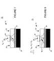
- FIG. 9Ais a cross-sectional schematic view of a memory cell according to aspects of the present inventions wherein the memory cell includes an active access element and transistor having an electrically floating body;
- FIGS. 9B and 9Care cross-sectional schematic views of two adjacent memory cells according to aspects of the present inventions wherein the active access element is shared between the adjacent memory cells, wherein FIG. 9B is a cross-sectional schematic view of two adjacent N-channel type memory cells and FIG. 9C is a cross-sectional schematic view of two adjacent P-channel type memory cells;
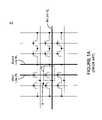
- FIG. 10illustrates an exemplary layout of the memory cells of FIGS. 9B and 9C , notably, access line 1 (AL 1 ) and access line 2 (AL 2 ) may be formed from a semiconductor (for example, monocrystalline or polycrystalline silicon (preferably doped), and/or a highly conductive material such as a metal or metal-like material, for example, aluminum, copper, or gold, and/or materials including aluminum, silver, tungsten, copper, and/or gold) according to at least one of the embodiments of the present inventions;
- a semiconductorfor example, monocrystalline or polycrystalline silicon (preferably doped)
- a highly conductive materialsuch as a metal or metal-like material, for example, aluminum, copper, or gold, and/or materials including aluminum, silver, tungsten, copper, and/or gold
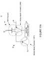
- FIG. 11Ais a schematic representation of an equivalent electrically floating body memory cell (N-channel type) including intrinsic bipolar transistors in addition to a MOS transistor;
- FIG. 11Bis a schematic representation of an equivalent electrically floating body memory cell (P-channel type) including intrinsic bipolar transistors in addition to a MOS transistor;
- FIG. 12illustrates exemplary timing relationships of selected write control signals to (i) program or write a logic state “1” into one or more N-channel type memory cells, (ii) program or write logic state “0” into one or more N-channel type memory cells, and (iii) read one or more N-channel type memory cells according to one embodiment of the present inventions;
- FIGS. 13A and 13Bare schematic block diagram illustrations of exemplary integrated circuit devices in which the memory cell array (and certain peripheral circuitry) may be implemented, according to certain aspects of the present inventions.
- FIG. 14is a schematic block diagram of an embodiment of an integrated circuit device including, among other things, a memory cell array, data sense and write circuitry, memory cell selection and control circuitry, according to certain aspects of the present inventions.
- Each memory cellincludes at least one transistor having an electrically floating body transistor and an active access element.
- the electrically floating body region of the transistorforms a storage area or node of the memory cell wherein an electrical charge which is representative of a data state is stored in the electrically floating body region.
- the active access elementis coupled to the electrically floating body transistor to facilitate programming of the memory cell and to provide a relatively large amount of majority carriers to the storage area or node of the memory cell during a write operation.
- the memory cell and/or memory cell array of the present inventionsmay be incorporated in an integrated circuit device, for example, a logic device (such as, for example, a microcontroller or microprocessor) or may comprise a portion of a memory device (such as, for example, a discrete memory).
- a logic devicesuch as, for example, a microcontroller or microprocessor
- a memory devicesuch as, for example, a discrete memory
- the present inventionsare directed to memory cell 12 having (i) electrically floating body transistor 14 to store a charge which is representative of a data state of memory cell 12 , and (ii) active access element 36 which facilitates programming of memory cell 12 during a write operation.
- transistor 14includes gate 16 , body region 18 , which is electrically floating, drain region 22 and control node 38 .
- the gate 16is disposed on a dielectric material above body region 18 .
- the body region 18is disposed between drain region 22 and control node 38 .
- body region 18is disposed on or above region 24 , which may be an insulation region (for example, in an SOI material/substrate) or non-conductive region (for example, in a bulk-type material/substrate).
- region 24may be an insulation region (for example, in an SOI material/substrate) or non-conductive region (for example, in a bulk-type material/substrate).
- the insulation or non-conductive region 24may be disposed on substrate 26 .
- transistor 14is electrically coupled to word line 28 , and drain region 22 is electrically coupled to bit line 32 .
- transistor 14may be an N-channel or P-channel type of transistor.
- the active access element 36facilitates programming of memory cell 12 .
- the active access element 36provides and/or injects majority carriers into electrically floating body region 18 of transistor 14 during a write operation of memory cell 12 .
- the active access element 36includes access regions and/or lines AL 1 and AL 2 (hereinafter collectively “access lines”).
- active access element 36further includes a dielectric material disposed between the first and second access lines AL 1 and AL 2 , respectively.
- active access element 36further includes control node 38 .
- access line AL 1may be an N-type, a P-type or an intrinsic semiconductor region.
- the access line AL 2may be a semiconductor region (for example, monocrystalline or polycrystalline silicon, preferably doped) and/or a highly conductive material such as a metal or metal-like material, for example, aluminum, copper, or gold, and/or materials including aluminum, copper, or gold.
- memory cell 12includes an N-channel type transistor 14 and active access element 36 having access line AL 1 which is a P-type semiconductor region. In another embodiment, memory cell 12 includes a P-channel type transistor 14 and active access element 36 having access line AL 1 which is an N-type semiconductor region. In yet another exemplary embodiment, memory cell 12 may include an N-channel type or P-channel type transistor 14 and active access element 36 having access line AL 1 which is an intrinsic semiconductor region.
- the access regions of active access element 36may be portions of access lines AL 1 and AL 2 which interact with the associated transistor 14 .
- access lines AL 1 and AL 2may electrically connect the access regions of active access element 36 (in a manner similar to a word line 28 connecting to a gate of a transistor 16 ).
- the access regions and/or lines AL 1 and AL 2 of an active access element 36are collectively identified “access lines” unless such aspect(s) of the active access element are/is stated as an “access region”.
- control signals each having a predetermined amplitudemay be selectively applied to memory cell 12 to write logic state “1”, write logic state “0”, and read the data state of memory cell 12 .
- signalsare applied to (i) gate 16 and drain region 22 of electrically floating body transistor 14 (via word line 18 and bit line 32 , respectively), and (ii) access line AL 1 and access line AL 2 of active access element 36 in order to write a data in memory cell 12 or read the data stored in memory cell 12 .
- a control signal having a voltage of +1.2Vis applied to access line AL 1 and a control signal having a voltage of 0V is applied to Access Line AL 2 .
- the logic state written into memory cell 12may be determined via application of suitable control signals to gate 16 (via word line 28 ) and drain region 22 (via bit line 32 ).
- a logic state “1”may be programmed or written in memory cell 12 by applying a voltage pulse of +1.2V to gate 16 of transistor 14 and 0V to drain region 22 of transistor 14 .
- a MOS transistor component of transistor 14 of memory cell 12is “on” (or substantially “on”) and the voltage of control node 38 is equal to (or substantially equal to) the voltage applied to drain region 22 (via bit line 32 ).
- an intrinsic bipolar transistor 1(BP 1 ) is also “on” and the majority carriers (in this example, holes) flow to electrically floating body region 18 (the storage node of memory cell 12 ).
- intrinsic bipolar transistor 1is formed by access lines AL 1 and AL 2 and control node 38 .
- the amplitude of the control signal applied to gate 16(via word line 28 ) is reduced to a “holding” condition or value (in this example, ⁇ 1.2V) and the amplitude of the control signal applied to drain region 22 is increased to a “holding” condition or value (in this example, +1.2V).
- the amplitude of the control signal applied to gate 16is reduced to a holding condition or value ( ⁇ 1.2V) after the control signal applied to drain region 22 is increased to a holding condition or value (+1.2V).
- the time interval ⁇ tis greater than zero.
- bit line control signalmay be applied to drain region 22 before the word line control signal is applied to gate 16 , simultaneously thereto, or after the pulse is applied to gate 16 of transistor 14 of memory cell 12 .
- the pulse applied to drain region 22includes an amplitude which is sufficient to maintain a bipolar current to program, write or store a logic state “1” into memory cell 12 .
- the bit line control signal(which is applied to drain region 22 ) extend beyond when the control signal applied to the word line (WL) reduces or ceases, as illustrated in FIG. 6 .
- a control signal having a voltage of +1.2Vis again applied to access line AL 1 and a control signal having a voltage of 0V is again applied to Access Line AL 2 .
- the logic state written into memory cell 12may be determined via application of suitable control signals to gate 16 (via word line 28 ) and drain region 22 (via bit line 32 ).
- control signals having predetermined amplitudesmay be applied to memory cell 12 to write, program or store logic state “0” therein.
- the word line control signal applied to gate 16 of transistor 14is raised to +1.2V and the bit line control signal applied to drain region 22 is +1.2V.
- the potential of storage area or node of memory cell 12 aincreases to a state whereby majority carriers are ejected, removed and/or forced from electrically floating body region 18 (the storage area or node of memory cell 12 ) of transistor 14 .
- memory cell 12may be placed or maintained in a standby condition or state (or in a “holding” condition or state), by applying a positive voltage (for example, +1.2V) to drain region 22 of transistor 14 and a negative voltage (for example, ⁇ 1.2V) to gate 16 (via word line 28 ).
- a positive voltagefor example, +1.2V
- a negative voltagefor example, ⁇ 1.2V
- the holding condition or statemay be applied or established to prevent, minimize or avoid disturbance of the data state of, and/or the charge contained in the storage area or node (electrically floating body region of the transistor) in an “unselected” memory cell.
- the data state of memory cell 12may be read, sensed, sampled and/or determined by applying control signals having predetermined amplitudes to gate 16 (via word line 28 ) and drain region 22 (via bit line 32 ) of transistor 14 .
- a read operationis implemented by applying (i) a signal having a voltage that is higher than the amplitude of the holding level (for example, ⁇ 1.2V) to gate 16 and (2) a signal having a voltage that is lower than the amplitude of the holding level (for example, +1.2V) to drain region 22 .
- memory cell 12may be read by applying 0 V to gate 16 and drain region 22 of transistor 14 .
- the bipolar transistor BP 2is “on” or substantially “on” in the event that memory cell 12 stores a “1” data state and the bipolar transistor BP 2 is “off” or substantially “off” (relative to when memory cell 12 stores a “1” data state) in the event that memory cell 12 a is in “0” data state.
- the current output by memory cell 12varies depending on whether memory cell 12 stores a logic state “1” or state “0”.
- data sensing circuitryincluding, for example, a current sense amplifier, may be used to measure the current and to identify the state of the memory cell.
- the illustrated/exemplary voltage levels to implement the write and read operationsare merely exemplary.
- the indicated voltage levelsmay be relative or absolute.
- the voltages indicatedmay be relative in that each voltage level, for example, may be increased or decreased by a given voltage amount (for example, each voltage may be increased or decreased by 0.25, 0.5, 1.0 and 2.0 volts) whether one or more of the voltages (for example, the source, drain or gate voltages) become or are positive and negative.
- the present inventionsmay include a memory cell array including a plurality of memory cells wherein each memory cell includes (i) an electrically floating body transistor to store a charge which is representative of a data state of the memory cell, and (ii) an active access element.
- each memory cellincludes (i) an electrically floating body transistor to store a charge which is representative of a data state of the memory cell, and (ii) an active access element.
- the present inventionsinclude a memory cell, having electrically floating body transistor (an N-channel type in the illustrative embodiment of FIG. 9B , and a P-channel type in the illustrative embodiment of FIG. 9C ) to store a charge which is representative of a data state of the memory cell.
- the active access element 36includes access lines AL 1 and AL 2 to provide input signals, as discussed above, into the memory cells to control, in conjunction or combination with other control signals, the memory cells (for example, the write operation (and the data state stored in the memory cell) and the read operation).
- the access linesare shared between two adjacent memory cells.
- each voltage levelmay be increased or decreased by a given voltage amount (for example, each voltage may be increased or decreased by 0.25, 0.5, 1.0 and 2.0 volts) whether one or more of the voltages (for example, the source, drain or gate voltages) become or are positive and negative.
- FIG. 10An exemplary layout of the memory cells of FIGS. 9B and 9C is illustrated in FIG. 10 .
- the layout of FIG. 10is a relatively compact in that adjacent memory cells share an active access element. All layouts, whether now known or later developed, for implementing the present inventions are intended to fall within the scope of the present inventions.
- the present inventionsmay be implemented in any electrically floating body memory cell 12 , plurality of memory cells 12 and memory cell array.
- a plurality of memory cells 12 of the present inventionsmay be implemented in a memory array having, for example, a plurality of rows and columns (for example, in a matrix form).
- the memory cells and memory cell array of the present inventionsmay be implemented in an integrated circuit device having a memory portion and a logic portion (see, for example, FIG. 13A ), or an integrated circuit device that is primarily a memory device (see, for example, FIG. 13B ).
- the memory arraymay include a plurality of memory cells arranged in a plurality of rows and columns wherein each memory cell includes an electrically floating body transistor.
- the memory arraysmay be comprised of N-channel, P-channel and/or both types of transistors.
- circuitry that is peripheral to the memory arrayfor example, data sense circuitry (for example, sense amplifiers or comparators), memory cell selection and control circuitry (for example, word line and/or source line drivers), as well as row and column address decoders) may include P-channel and/or N-channel type transistors.
- the integrated circuit devicemay include array 10 , having a plurality of memory cells 12 , data write and sense circuitry 40 , and memory cell selection and control circuitry 42 .
- the data write and sense circuitry 40reads data from and writes data to selected memory cells 12 .
- data write and sense circuitry 40includes a plurality of data sense amplifiers. Each data sense amplifier receives at least one bit line 32 and an output of reference generator circuitry (for example, a current or voltage reference signal).
- the memory arraysmay be comprised of an N-channel, a P-channel and/or both types of transistors.
- circuitry that is peripheral to the memory arrayfor example, sense amplifiers or comparators, row and column address decoders, as well as line drivers (not illustrated herein) may include P-channel and/or N-channel type transistors.
- P-channel type transistorsare employed as memory cells 12 in the memory array(s)
- suitable write and read voltagesfor example, negative voltages
- the memory cell(s), memory array and techniques for operating (for example, reading, writing, restoring and refreshing) such memory cell(s) and/or arrays of the present inventionsmay be employed in conjunction with any architecture, layout, structure, control circuitry and/or configuration employing such electrically floating body memory cells (among other types of memory cells).
- the memory cell(s) and memory array of the present inventionsmay be implemented in the architecture, layout, structure, control circuitry and/or configuration described and illustrated in the following U.S. patent applications:
- the memory cellsmay be controlled (for example, programmed or read) using any of the control circuitry described and illustrated in the above-referenced ten (10) U.S. patent applications.
- control circuitrydescribed and illustrated in the above-referenced ten (10) U.S. patent applications.
- all memory cell selection and control circuitry, and techniques for programming, reading, controlling and/or operating memory cells including transistors having strained electrically floating body regions, whether now known or later developed,are intended to fall within the scope of the present inventions.
- the data stored in or written into memory cells 12may be read using any circuitry and/or technique (whether conventional or not), including those described in the above-referenced ten (10) U.S. patent applications.
- the data write and sense circuitrymay include a sense amplifier to read the data stored in memory cells 12 .
- the sense amplifierfor example, a cross-coupled sense amplifier as described and illustrated in the (1) U.S. patent application Ser. No. 11/299,590 ((U.S. Patent Application Publication No. 2006/0126374), which was filed by Waller and Carman, on Dec. 12, 2005 and entitled “Sense Amplifier Circuitry and Architecture to Write Data into and/or Read from Memory Cells”, and/or (2) U.S. patent application Ser. No. 10/840,902, which was filed by Portmann et al. on May 7, 2004, and entitled “Reference Current Generator, and Method of Programming, Adjusting and/or Operating Same”, now U.S. Pat. No.
- 6,912,150may sense the data state stored in memory cell 12 using voltage or current sensing circuitry and/or techniques.
- the current sense amplifiermay compare the cell current to a reference current, for example, the current of a reference cell (not illustrated). From that comparison, it may be determined whether memory cell 12 contained a logic high (relatively more majority carries 34 contained within body region 18 ) or logic low data state (relatively less majority carries 28 contained within body region 18 ).
- a logic highrelatively more majority carries 34 contained within body region 18
- logic low data staterespectively less majority carries 28 contained within body region 18
- the present inventionsmay employ the reference generation techniques (used in conjunction with the data sense circuitry for the read operation) U.S. Non-Provisional patent application Ser. No. 11/515,667, which was filed by Bauser on Sep. 5, 2006, and entitled “Method and Circuitry to Generate a Reference Current for Reading a Memory Cell, and Device Implementing Same” (identified above). Indeed, the present inventions may also employ the read circuitry, architectures and techniques described and illustrated in U.S. Pat. No. 6,912,150, identified above.
- each memory cell 12 in the exemplary embodimentsincludes at least one transistor 14
- memory cell 12may include a differential transistor pair, as described and illustrated in application Ser. No. 10/829,877, which was filed by Ferrant et al. on Apr. 22, 2004 and entitled “Semiconductor Memory Cell, Array, Architecture and Device, and Method of Operating Same” (U.S. Patent Application Publication No. 2005/0013163, now U.S. Pat. No. 7,085,153).
- any of the architectures, layouts, structures and/or configurations, as well as the programming and reading operations described and illustrated in application Ser. No. 10/829,877may be employed in conjunction with the inventions described and illustrated herein. For the sake of brevity, those discussions will not be repeated; rather, they are incorporated by reference herein.
- the electrically floating memory cells, transistors and/or memory array(s)may be fabricated using well known techniques and/or materials. Indeed, any fabrication technique and/or material, whether now known or later developed, may be employed to fabricate the electrically floating body memory cells, transistors and/or memory array(s).
- the present inventionsmay employ silicon (whether bulk-type or SOI), germanium, silicon/germanium, gallium arsenide or any other semiconductor material in which transistors may be formed.
- the electrically floating transistors, memory cells, and/or memory array(s)may employ the techniques described and illustrated in (1) non-provisional patent application entitled “Integrated Circuit Device, and Method of Fabricating Same”, which was filed on Jul. 2, 2004, by Fazan, Ser. No.
- memory array 10may be integrated with SOI logic transistors, as described and illustrated in the Integrated Circuit Device Patent Applications.
- an integrated circuit deviceincludes memory section (having, for example, PD or FD SOI memory transistors 14 ) and logic section (having, for example, high performance transistors, such as FinFET, multiple gate transistors, and/or non-high performance transistors (for example, single gate transistors that do not possess the performance characteristics of high performance transistors—not illustrated)).
- memory sectionhaving, for example, PD or FD SOI memory transistors 14
- logic sectionhaving, for example, high performance transistors, such as FinFET, multiple gate transistors, and/or non-high performance transistors (for example, single gate transistors that do not possess the performance characteristics of high performance transistors—not illustrated)).
- the entire contents of the Integrated Circuit Device Patent Applicationsincluding, for example, the inventions, features, attributes, architectures, configurations, materials, techniques and advantages described and illustrated therein, are hereby incorporated by reference.
- the memory arraysmay be comprised of N-channel, P-channel and/or both types of transistors, as well as partially depleted and/or fully depleted type transistors.
- circuitry that is peripheral to the memory arraymay include fully depleted type transistors (whether P-channel and/or N-channel type).
- circuitrymay include partially depleted type transistors (whether P-channel and/or N-channel type).
- the electrically floating body transistor 14may be a symmetrical or non-symmetrical device. Where transistor 14 is symmetrical, the source and drain regions are essentially interchangeable. However, where transistor 14 is a non-symmetrical device, the source or drain regions of transistor 14 have different electrical, physical, doping concentration and/or doping profile characteristics. As such, the source or drain regions of a non-symmetrical device are typically not interchangeable. This notwithstanding, the drain region of the electrically floating N-channel transistor of the memory cell (whether the source and drain regions are interchangeable or not) is that region of the transistor that is connected to the bit line/sense amplifier.
- the illustrated/exemplary voltage levels to implement the read and write operationsare merely exemplary.
- the indicated voltage levelsmay be relative or absolute.
- the voltages indicatedmay be relative in that each voltage level, for example, may be increased or decreased by a given voltage amount (for example, each voltage may be increased or decreased by 0.1, 0.15, 0.25, 0.5, 1 volt) whether one or more of the voltages (for example, the source, drain or gate voltages) become or are positive and negative.
- the access regions of active access element 36may be portions of access lines AL 1 and AL 2 which interact with the associated transistor 14 or the access regions of active access element 36 may electrically connect to access lines AL 1 and AL 2 (in a manner similar to a word line 28 connecting to a gate of a transistor 16 ).
- the access regions and/or lines AL 1 and AL 2 of an active access element 36are collectively identified “access lines” unless such aspect(s) of the active access element is/are stated as an “access region”, for example, as set forth in certain of the claims.
Landscapes
- Engineering & Computer Science (AREA)
- Microelectronics & Electronic Packaging (AREA)
- Computer Hardware Design (AREA)
- Semiconductor Memories (AREA)
- Non-Volatile Memory (AREA)
Abstract
Description
- This application claims priority to U.S. Provisional Application Ser. No. 60/751,505, entitled “Floating Body Memory Cell and Array, and Method of Operating or Controlling Same”, filed Dec. 19, 2005; the contents of the provisional application are incorporated by reference herein in its entirety.
- The inventions relate to a semiconductor memory cell, array, architecture and device, and techniques for reading, controlling and/or operating such cell and device; and more particularly, in one aspect, to a semiconductor dynamic random access memory (“DRAM”) cell, array, architecture and/or device wherein the memory cell includes an electrically floating body in which an electrical charge is stored.
- There is a continuing trend to employ and/or fabricate advanced integrated circuits using techniques, materials and devices that improve performance, reduce leakage current and enhance overall scaling. Semiconductor-on-Insulator (SOI) is a material in which such devices may be fabricated or disposed on or in (hereinafter collectively “on”). Such devices are known as SOI devices and include, for example, partially depleted (PD), fully depleted (FD) devices, multiple gate devices (for example, double or triple gate), and Fin-FET.
- One type of dynamic random access memory cell is based on, among other things, the electrically floating body effect of SOI transistors. (See, for example, U.S. Pat. No. 6,969,662, incorporated herein by reference). In this regard, the dynamic random access memory cell may consist of a PD or a FD SOI transistor (or transistor formed in bulk material/substrate) on having a channel, which is disposed adjacent to the body and separated therefrom by a gate dielectric. The body region of the transistor is electrically floating in view of the insulation layer (or non-conductive region, for example, in a bulk-type material/substrate) disposed beneath the body region. The state of memory cell is determined by the concentration of charge within the body region of the SOI transistor.
- With reference to
FIGS. 1A ,1B and1C, in one exemplary embodiment,semiconductor DRAM array 10 includes a plurality ofmemory cells 12 each consisting oftransistor 14 havinggate 16,body region 18, which is electrically floating,source region 20 anddrain region 22. Thegate 16 is disposed on a dielectric material abovebody region 18. Thebody region 18 is disposed betweensource region 20 and drainregion 22. Moreover,body region 18 is disposed on or aboveregion 24, which may be an insulation region (for example, in an SOI material/substrate) or non-conductive region (for example, in a bulk-type material/substrate). The insulation or non-conductiveregion 24 may be disposed onsubstrate 26. - Data is written into or read from a selected memory cell by applying suitable control signals to a selected word line(s)28, a selected source line(s)30 and/or a selected bit line(s)32. In response, charge carriers are accumulated in or emitted and/or ejected from electrically floating
body region 18 wherein the data states are defined by the amount of carriers within electrically floatingbody region 18. Notably, the entire contents of the '662 patent, including, for example, the features, attributes, architectures, configurations, materials, techniques and advantages described and illustrated therein, are incorporated by reference herein. - As mentioned above,
memory cell 12 ofDRAM array 10 operates by accumulating in or emitting/ejecting majority carriers (electrons or holes)34 frombody region 18 of, for example, N-channel transistors. (See,FIGS. 2A and 2B ). In this regard, accumulating majority carriers (in this example, “holes”)34 inbody region 18 ofmemory cells 12 via, for example, impact ionization nearsource region 20 and/ordrain region 22, is representative of a logic high or “1” data state. (See,FIG. 2A ). Emitting or ejectingmajority carriers 30 frombody region 18 via, for example, forward biasing the source/body junction and/or the drain/body junction, is representative of a logic low or “0” data state. (See,FIG. 2B ). - Notably, for at least the purposes of this discussion, a logic high or State “1” corresponds to an increased concentration of majority carriers in the body region relative to an unprogrammed device and/or a device that is programmed with a logic low or State “0”. In contrast, a logic low or State “0” corresponds to a reduced concentration of majority carriers in the body region relative to an unprogrammed device and/or a device that is programmed with logic high or State “1”.
- Conventional reading is performed by applying a small drain bias and a gate bias above the transistor threshold voltage. The sensed drain current is determined by the charge stored in the floating body giving a possibility to distinguish between the states “1” and “0”. A floating body memory device has two different current states corresponding to the two different logical states: “1” and “0”.
- In one conventional technique, the memory cell is read by applying a small bias to the drain of the transistor as well as a gate bias which is above the threshold voltage of the transistor. In this regard, in the context of memory cells employing N-type transistors, a positive voltage is applied to one or
more word lines 28 to enable the reading of the memory cells associated with such word lines. The amount of drain current is determined/affected by the charge stored in the electrically floating body region of the transistor. As such, conventional reading techniques sense the amount of the channel current provided/generated in response to the application of a predetermined voltage on the gate of the transistor of the memory cell to determine the state of the memory cell; a floating body memory cell may have two or more different current states corresponding to two or more different logical states (for example, two different current conditions/states corresponding to the two different logical states: “1” and “0”). - In short, conventional writing programming techniques for memory cells having an N-channel type transistor often provide an excess of majority carriers by channel impact ionization (see,
FIG. 3A ) or by band-to-band tunneling (gate-induced drain leakage “GIDL”) (see,FIG. 3B ). The majority carrier may be removed via drain side hole removal (see,FIG. 4A ), source side hole removal (see,FIG. 4B ), or drain and source hole removal, for example, using the back gate pulsing (see,FIG. 4C ). - The
memory cell 12 having electrically floatingbody transistor 14 may be programmed/read using other techniques including techniques that may, for example, provide lower power consumption relative to conventional techniques. For example,memory cell 12 may be programmed, read and/or controlled using the techniques and circuitry described and illustrated in U.S. Non-Provisional patent application Ser. No. 11/509,188, filed on Aug. 24, 2006, and entitled “Memory Cell and Memory Cell Array Having an Electrically Floating Body Transistor, and Methods of Operating Same” (hereinafter “the '188 application”), which is incorporated by reference herein. In one aspect, the '188 application is directed to programming, reading and/or control methods which allow low power memory programming and provide larger memory programming window (both relative to at least the conventional programming techniques). - With reference to
FIG. 5 , in one exemplary embodiment, the '188 application employs, writes or programs a logic “1” or logic high using control signals (having predetermined voltages, for example, Vg=0v, Vs=0v, and Vd=2.5v) which are applied togate 16,source region 20 and drain region22 (respectively) oftransistor 14 ofmemory cell 12. Such control signals induce or cause impact ionization and/or the avalanche multiplication phenomenon (FIG. 5 ). The predetermined voltages of the control signals, in contrast to the conventional method program or write logic “1” in the transistor of the memory cell via impact ionization and/or avalanche multiplication in the electrically floating body. In one embodiment, it is preferred that the bipolar transistor current responsible for impact ionization and/or avalanche multiplication in the floating body is initiated and/or induced by a control pulse which is applied togate 16. Such a pulse may induce the channel impact ionization which increases the floating body potential and turns on the bipolar current. An advantage of the described method is that larger amount of the excess majority carriers is generated compared to other techniques. - Further, with reference to
FIG. 6 , when writing or programming logic “0” intransistor 14 ofmemory cell 12, in one embodiment of the '188 application, the control signals (having predetermined voltages (for example, Vg=1.5v, Vs=0v and Vd=0v) are different and, in at least one embodiment, higher than a holding voltage (if applicable)) are applied togate 16,source region 20 and drain region22 (respectively) oftransistor 14 ofmemory cell 12. Such control signals induce or provide removal of majority carriers from the electrically floating body oftransistor 14. In one embodiment, the majority carriers are removed, eliminated or ejected frombody region 18 throughsource region 20 anddrain region 22. (See,FIG. 6 ). In this embodiment, writing orprogramming memory cell 12 with logic “0” may again consume lower power relative to conventional techniques. - When
memory cell 12 is implemented in a memory cell array configuration, it may be advantageous to implement a “holding” operation forcertain memory cells 12 when programming one or moreother memory cells 12 of the memory cell array to enhance the data retention characteristics of suchcertain memory cells 12. Thetransistor 14 ofmemory cell 12 may be placed in a “holding” state via application of control signals (having predetermined voltages) that are applied togate 16 andsource region 20 anddrain region 22 oftransistor 14 ofmemory cell 12. In combination, such control signals provide, cause and/or induce majority carrier accumulation in an area that is close to the interface between gate dielectric32 and electrically floatingbody region 18. (See,FIG. 7 ). In this embodiment, it may be preferable to apply a negative voltage togate 16 wheretransistor 14 is an N-channel type transistor. - With reference to
FIG. 8 , in one embodiment of the '188 application, the data state ofmemory cell 12 may be read and/or determined by applying control signals (having predetermined voltages, for example, Vg=−0.5v, Vs=2.5v and Vd=0v) togate 16 andsource region 20 and drainregion 22 oftransistor 14. Such signals, in combination, induce and/or cause the bipolar transistor current in thosememory cells 12 storing a logic state “1”. For those memory cells that are programmed to a logic state “0”, such control signals do not induce and/or cause a considerable, substantial or sufficiently measurable bipolar transistor current in the cells programmed to “0” state. (See, the '188 application, which, as noted above, is incorporated by reference). - As mentioned above, the reading may be performed using positive voltages applied to word lines28. As such,
transistors 14 ofdevice 10 are periodically pulsed between a positive gate bias, which (1) drives majority carriers (holes for N-channel transistors) away from the interface betweengate insulator 32 andbody region 18 oftransistor 14 and (2) causes minority carriers (electrons for N-channel transistors) to flow fromsource region 20 and drainregion 22 into a channel formed belowgate 16, and the negative gate bias, which causes majority carriers (holes for N-channel transistors) to accumulate in or near the interface betweengate 16 andbody region 18 oftransistor 14. - Notably, conventional programming techniques may employ relatively high drain and/or gate bias voltages, which may increase the power consumption of the memory cell. Moreover, relatively high bias voltages may present device scaling challenges due to the reduction in device features. The proposed memory cell does not require any high voltages and provides a low power and scalable memory.
- There are many inventions described and illustrated herein. The present inventions are neither limited to any single aspect nor embodiment thereof, nor to any combinations and/or permutations of such aspects and/or embodiments. Moreover, each of the aspects of the present inventions, and/or embodiments thereof, may be employed alone or in combination with one or more of the other aspects of the present inventions and/or embodiments thereof. For the sake of brevity, many of those permutations and combinations will not be discussed separately herein.
- In one aspect, the present inventions are directed to a semiconductor memory cell, memory cell array including a plurality of memory cells. In another aspect, the present inventions are directed to techniques for reading, controlling and/or operating, the memory cell and/or memory cell array. Each memory cell includes at least one transistor having an electrically floating body transistor and an active access element. The electrically floating body region of the transistor forms a storage area or node of the memory cell wherein an electrical charge which is representative of a data state is stored in the electrically floating body region. The active access element is coupled to the electrically floating body transistor to facilitate programming of the memory cell and to provide a relatively large amount of majority carriers to the storage area or node of the memory cell during a write operation. The memory cell and/or memory cell array of the present inventions may be incorporated in an integrated circuit device, for example, a logic device (such as, for example, a microcontroller or microprocessor) or may comprise a portion of a memory device (such as, for example, a discrete memory).
- In another aspect, the present inventions are directed to an integrated circuit, disposed in or on a semiconductor region or layer which resides on or above a non-conducting region or layer of a substrate (for example, a bulk-type substrate (for example, silicon) or a semiconductor-on-insulator substrate), the integrated circuit comprises a semiconductor memory cell including (1) an active access element, electrically coupled to the transistor, including a first access line or region, a second access line or region, and a control node (for example, a region), and (2) a transistor including: (i) a first semiconductor region including impurities to provide a first conductivity type, (ii) a second semiconductor region including impurities to provide the first conductivity type, and (iii) a body region disposed between the first region, the second region and the non-conducting region or layer of the substrate, wherein the body region is electrically floating and includes impurities to provide a second conductivity type wherein the second conductivity type is different from the first conductivity type. The transistor also includes a gate spaced apart from the body region.
- The memory cell includes a first data state which corresponds to a first charge in the body region of the transistor of the memory cell, and (ii) a second data state which corresponds to a second charge in the body region of the transistor of the memory cell.
- In an exemplary embodiment, the first access line is a semiconductor region including impurities to provide the second conductivity type. In another exemplary embodiment, the first access line is a semiconductor region having a conductivity type which is different from the first conductivity type. The second access line may be a semiconductor material (for example, a doped semiconductor material) or metal material.
- In an exemplary embodiment, the control node of the active access element and the second semiconductor region of the transistor are a common region. In another embodiment, the active access element further includes a dielectric, disposed between the first access line/region and the second access line/region.
- In another aspect, the present inventions are directed to an integrated circuit, disposed in or on a semiconductor region or layer which resides on or above a non-conducting region or layer of a substrate (for example, a bulk-type substrate (for example, silicon) or a semiconductor-on-insulator substrate), the integrated circuit comprises a plurality of semiconductor memory cells arranged in a matrix of rows and columns, each semiconductor memory cell includes a transistor and an active access element, wherein the transistor is electrically coupled to the active access element. The active access element includes a first access line or region, a second access line or region and a control node (for example, a region). The transistor includes (i) a first semiconductor region including impurities to provide a first conductivity type, (ii) a second semiconductor region including impurities to provide the first conductivity type, and (iii) a body region disposed between the first region, the second region and the non-conducting region or layer of the substrate, wherein the body region is electrically floating and includes impurities to provide a second conductivity type wherein the second conductivity type is different from the first conductivity type. The transistor also includes a gate spaced apart from the body region.
- Each memory cell includes a first data state which corresponds to a first charge in the body region of the transistor of the memory cell, and (ii) a second data state which corresponds to a second charge in the body region of the transistor of the memory cell.
- In an exemplary embodiment, the first access line is a semiconductor region including impurities to provide the second conductivity type. In another exemplary embodiment, the first access line is a semiconductor region having a conductivity type which is different from the first conductivity type. The second access line may be a semiconductor material (for example, a doped semiconductor material) or metal material.
- In an exemplary embodiment, two adjacent memory cells share an active access element; in another embodiment, two adjacent memory cells share at least a portion of the first access line or region of the associated active access element.
- In an exemplary embodiment, the control node of the active access element and the second semiconductor region of the transistor are a common region. In another embodiment, the active access element further includes a dielectric, disposed between the first access line and the second access line.
- In another aspect, the present inventions are directed to an integrated circuit device comprising a memory cell array including a plurality of word lines, plurality of bit lines, a plurality of first access lines, and a plurality of second access lines. The integrated circuit further includes a plurality of semiconductor memory cells arranged in a matrix of rows and columns, each semiconductor memory cell includes a transistor and an active access element, wherein the transistor is electrically coupled to the active access element. The active access element includes a first access region (electrically coupled to the first access line), a second access region (electrically coupled to the second access line) and a control node (for example, a region). The transistor includes (i) a first semiconductor region electrically coupled to an associated bit line and including impurities to provide a first conductivity type, (ii) a second semiconductor region including impurities to provide the first conductivity type, and (iii) a body region disposed between the first region, the second region and the non-conducting region or layer of the substrate, wherein the body region is electrically floating and includes impurities to provide a second conductivity type wherein the second conductivity type is different from the first conductivity type. The transistor also includes a gate electrically coupled to an associated word line and spaced apart from the body region.
- Each memory cell includes a first data state which corresponds to a first charge in the body region of the transistor of the memory cell, and (ii) a second data state which corresponds to a second charge in the body region of the transistor of the memory cell.
- In an exemplary embodiment, the first access line is a semiconductor region including impurities to provide the second conductivity type. In another exemplary embodiment, the first access line is a semiconductor region having a conductivity type which is different from the first conductivity type. The second access line may be a semiconductor material (for example, a doped semiconductor material) or metal material.
- In an exemplary embodiment, two adjacent memory cells share an active access element; in another embodiment, two adjacent memory cells share at least a portion of the first access line or region of the associated active access element. Indeed, in another embodiment, the first semiconductor region of the transistors of the two adjacent memory cells are connected to the same bit line.
- In an exemplary embodiment, the control node of the active access element and the second semiconductor region of the transistor are a common region. In another exemplary embodiment, the active access element further includes a dielectric, disposed between the first access line and the second access line.
- Again, there are many inventions, and aspects of the inventions, described and illustrated herein. This Summary of the Inventions is neither exhaustive of the scope of the present inventions nor is it representative of the scope of the claims. This Summary of the Inventions is not intended to be limiting of the inventions and should not be interpreted in that manner. While certain embodiments have been described and/or outlined in this Summary of the Inventions, it should be understood that the present inventions are not limited to such embodiments, description and/or outline, nor are the claims limited in such a manner. Indeed, many other embodiments, which may be different from and/or similar to, the embodiments presented in this Summary, will be apparent from the description, illustrations and claims, which follow. In addition, although various features, attributes and advantages have been described in this Summary of the Inventions and/or are apparent in light thereof, it should be understood that such features, attributes and advantages are not required whether in one, some or all of the embodiments of the present inventions and, indeed, need not be present in any of the embodiments of the present inventions.
- In the course of the detailed description to follow, reference will be made to the attached drawings. These drawings show different aspects of the present inventions and, where appropriate, reference numerals illustrating like structures, components, materials and/or elements in different figures may be labeled similarly. It is understood that various combinations of the structures, components, materials and/or elements, other than those specifically shown, are contemplated and are within the scope of the present inventions.
- Moreover, as noted above, there are many inventions described and illustrated herein. The present inventions are neither limited to any single aspect nor embodiment thereof, nor to any combinations and/or permutations of such aspects and/or embodiments. Moreover, each of the aspects of the present inventions, and/or embodiments thereof, may be employed alone or in combination with one or more of the other aspects of the present inventions and/or embodiments thereof. For the sake of brevity, many of those permutations and combinations will not be discussed separately herein.
FIG. 1A is a schematic representation of a prior art DRAM array including a plurality of memory cells comprised of one electrically floating body transistor;FIG. 1B is a three dimensional view of an exemplary prior art memory cell comprised of one electrically floating body transistor (PD-SOI NMOS);FIG. 1C is a cross-sectional view of the prior art memory cell ofFIG. 1B , cross-sectioned along line C-C′;FIGS. 2A and 2B are exemplary schematic illustrations of the charge relationship, for a given data state, of the floating body, source and drain regions of a prior art memory cell comprised of one electrically floating body transistor (PD-SOI NMOS);FIGS. 3A and 3B are exemplary schematic and general illustrations of conventional methods to program a memory cell to logic state “1” (i.e., generate or provide an excess of majority carrier in the electrically floating body of the transistor (an N-type channel transistor in this exemplary embodiment) of the memory cell ofFIG. 1B ; majority carriers in these exemplary embodiments are generated or provided by the channel electron impact ionization (FIG. 3A ) and by GIDL or band to band tunneling (FIG. 3B );FIGS. 4A-4C are exemplary schematics and general illustrations of conventional methods to program a memory cell to logic state “0” (i.e., provide relatively fewer majority carrier by removing majority carriers from the electrically floating body of the transistor of the memory cell ofFIG. 1B ; majority carriers may be removed through the drain region/terminal of the transistor (FIG. 4A ), the source region/terminal of the transistor (FIG. 4B ), and through both drain and source regions/terminals of the transistor via using the back gate pulses applied to the substrate/backside terminal of the transistor of the memory cell (FIG. 4C );FIG. 5 illustrates an exemplary schematic (and control signal voltage relationship) of an exemplary embodiment of an aspect of the '188 application of programming a memory cell to logic state “1” by generating, storing and/or providing an excess of majority carriers in the electrically floating body of the transistor of the memory cell;FIG. 6 illustrates an exemplary schematic (and control signals) of an exemplary embodiment of an aspect of the '188 application of programming a memory cell to a logic state “0” by generating, storing and/or providing relatively fewer majority carriers (as compared to the number of majority carriers in the electrically floating body of the memory cell that is programmed to a logic state “1”) in the electrically floating body of the transistor of the memory cell, wherein the majority carriers are removed (write “0”) through both drain and source terminals by applying a control signal (for example, a programming pulse) to the gate of the transistor of the memory cell;FIG. 7 illustrates an exemplary schematic (and control signals) of an exemplary embodiment of an aspect of the '188 application of holding or maintaining the data state of a memory cell;FIG. 8 illustrates an exemplary schematic (and control signals) of an exemplary embodiment of an aspect of the '188 application of reading the data state of a memory cell by sensing the amount of the current provided/generated in response to an application of a predetermined voltage on the gate of the transistor of the memory cell;FIG. 9A is a cross-sectional schematic view of a memory cell according to aspects of the present inventions wherein the memory cell includes an active access element and transistor having an electrically floating body;FIGS. 9B and 9C are cross-sectional schematic views of two adjacent memory cells according to aspects of the present inventions wherein the active access element is shared between the adjacent memory cells, whereinFIG. 9B is a cross-sectional schematic view of two adjacent N-channel type memory cells andFIG. 9C is a cross-sectional schematic view of two adjacent P-channel type memory cells;FIG. 10 illustrates an exemplary layout of the memory cells ofFIGS. 9B and 9C , notably, access line1 (AL1) and access line2 (AL2) may be formed from a semiconductor (for example, monocrystalline or polycrystalline silicon (preferably doped), and/or a highly conductive material such as a metal or metal-like material, for example, aluminum, copper, or gold, and/or materials including aluminum, silver, tungsten, copper, and/or gold) according to at least one of the embodiments of the present inventions;FIG. 11A is a schematic representation of an equivalent electrically floating body memory cell (N-channel type) including intrinsic bipolar transistors in addition to a MOS transistor;FIG. 11B is a schematic representation of an equivalent electrically floating body memory cell (P-channel type) including intrinsic bipolar transistors in addition to a MOS transistor;FIG. 12 illustrates exemplary timing relationships of selected write control signals to (i) program or write a logic state “1” into one or more N-channel type memory cells, (ii) program or write logic state “0” into one or more N-channel type memory cells, and (iii) read one or more N-channel type memory cells according to one embodiment of the present inventions;FIGS. 13A and 13B are schematic block diagram illustrations of exemplary integrated circuit devices in which the memory cell array (and certain peripheral circuitry) may be implemented, according to certain aspects of the present inventions; andFIG. 14 is a schematic block diagram of an embodiment of an integrated circuit device including, among other things, a memory cell array, data sense and write circuitry, memory cell selection and control circuitry, according to certain aspects of the present inventions.- The present inventions describe a semiconductor memory cell, memory cell array, and techniques for reading, controlling and/or operating, the memory cell, and/or array. Each memory cell includes at least one transistor having an electrically floating body transistor and an active access element. The electrically floating body region of the transistor forms a storage area or node of the memory cell wherein an electrical charge which is representative of a data state is stored in the electrically floating body region. The active access element is coupled to the electrically floating body transistor to facilitate programming of the memory cell and to provide a relatively large amount of majority carriers to the storage area or node of the memory cell during a write operation. Notably, the memory cell and/or memory cell array of the present inventions may be incorporated in an integrated circuit device, for example, a logic device (such as, for example, a microcontroller or microprocessor) or may comprise a portion of a memory device (such as, for example, a discrete memory).
- With reference to
FIG. 9A , in one exemplary embodiment, the present inventions are directed tomemory cell 12 having (i) electrically floatingbody transistor 14 to store a charge which is representative of a data state ofmemory cell 12, and (ii)active access element 36 which facilitates programming ofmemory cell 12 during a write operation. In this embodiment,transistor 14 includesgate 16,body region 18, which is electrically floating,drain region 22 andcontrol node 38. Thegate 16 is disposed on a dielectric material abovebody region 18. Thebody region 18 is disposed betweendrain region 22 andcontrol node 38. Moreover,body region 18 is disposed on or aboveregion 24, which may be an insulation region (for example, in an SOI material/substrate) or non-conductive region (for example, in a bulk-type material/substrate). The insulation ornon-conductive region 24 may be disposed onsubstrate 26. - The
gate 16 is electrically coupled toword line 28, and drainregion 22 is electrically coupled tobit line 32. Notably,transistor 14 may be an N-channel or P-channel type of transistor. - In one exemplary embodiment, the
active access element 36 facilitates programming ofmemory cell 12. Theactive access element 36 provides and/or injects majority carriers into electrically floatingbody region 18 oftransistor 14 during a write operation ofmemory cell 12. Theactive access element 36 includes access regions and/or lines AL1 and AL2 (hereinafter collectively “access lines”). In addition, in this embodiment,active access element 36 further includes a dielectric material disposed between the first and second access lines AL1 and AL2, respectively. - Moreover, in operation,
active access element 36 further includescontrol node 38. Notably, access line AL1 may be an N-type, a P-type or an intrinsic semiconductor region. The access line AL2 may be a semiconductor region (for example, monocrystalline or polycrystalline silicon, preferably doped) and/or a highly conductive material such as a metal or metal-like material, for example, aluminum, copper, or gold, and/or materials including aluminum, copper, or gold. - In one exemplary embodiment,
memory cell 12 includes an N-channel type transistor 14 andactive access element 36 having access line AL1 which is a P-type semiconductor region. In another embodiment,memory cell 12 includes a P-channel type transistor 14 andactive access element 36 having access line AL1 which is an N-type semiconductor region. In yet another exemplary embodiment,memory cell 12 may include an N-channel type or P-channel type transistor 14 andactive access element 36 having access line AL1 which is an intrinsic semiconductor region. - Notably, with reference to
FIGS. 9A and 10 , in a memory cell array configuration/environment, the access regions ofactive access element 36 may be portions of access lines AL1 and AL2 which interact with the associatedtransistor 14. Alternatively, access lines AL1 and AL2 may electrically connect the access regions of active access element36 (in a manner similar to aword line 28 connecting to a gate of a transistor16). As noted above, the access regions and/or lines AL1 and AL2 of anactive access element 36 are collectively identified “access lines” unless such aspect(s) of the active access element are/is stated as an “access region”. - With reference to
FIGS. 9A ,11A and12, control signals each having a predetermined amplitude may be selectively applied tomemory cell 12 to write logic state “1”, write logic state “0”, and read the data state ofmemory cell 12. In particular, during a given memory operation, signals are applied to (i)gate 16 and drainregion 22 of electrically floating body transistor14 (viaword line 18 and bitline 32, respectively), and (ii) access line AL1 and access line AL2 ofactive access element 36 in order to write a data inmemory cell 12 or read the data stored inmemory cell 12. For example, in one exemplary embodiment to write logic state “1” intomemory cell 12 which includes an N-channel type transistor 14 andactive access element 36 having access line AL1 which is a P-type semiconductor region, a control signal having a voltage of +1.2V is applied to access line AL1 and a control signal having a voltage of 0V is applied to Access Line AL2. In this way, the logic state written intomemory cell 12 may be determined via application of suitable control signals to gate16 (via word line28) and drain region22 (via bit line32). - In particular, in this exemplary embodiment, a logic state “1” may be programmed or written in
memory cell 12 by applying a voltage pulse of +1.2V togate 16 oftransistor 14 and 0V to drainregion 22 oftransistor 14. Under these conditions, a MOS transistor component oftransistor 14 ofmemory cell 12 is “on” (or substantially “on”) and the voltage ofcontrol node 38 is equal to (or substantially equal to) the voltage applied to drain region22 (via bit line32). Moreover, an intrinsic bipolar transistor1 (BP1) is also “on” and the majority carriers (in this example, holes) flow to electrically floating body region18 (the storage node of memory cell12). Notably, intrinsicbipolar transistor 1 is formed by access lines AL1 and AL2 andcontrol node 38. - Thereafter, the amplitude of the control signal applied to gate16 (via word line28) is reduced to a “holding” condition or value (in this example, −1.2V) and the amplitude of the control signal applied to drain
region 22 is increased to a “holding” condition or value (in this example, +1.2V). In a preferred embodiment, the amplitude of the control signal applied togate 16 is reduced to a holding condition or value (−1.2V) after the control signal applied to drainregion 22 is increased to a holding condition or value (+1.2V). As such, with reference toFIG. 12 , the time interval Δt is greater than zero. - Notably, the bit line control signal may be applied to drain
region 22 before the word line control signal is applied togate 16, simultaneously thereto, or after the pulse is applied togate 16 oftransistor 14 ofmemory cell 12. It is preferred that the pulse applied to drain region22 (via bit line32) includes an amplitude which is sufficient to maintain a bipolar current to program, write or store a logic state “1” intomemory cell 12. As mentioned above, from a relative timing perspective, it is preferred that the bit line control signal (which is applied to drain region22) extend beyond when the control signal applied to the word line (WL) reduces or ceases, as illustrated inFIG. 6 . - With continued reference to
FIGS. 9A ,11A and12, in this exemplary embodiment, a control signal having a voltage of +1.2V is again applied to access line AL1 and a control signal having a voltage of 0V is again applied to Access Line AL2. As noted above, under these conditions, the logic state written intomemory cell 12 may be determined via application of suitable control signals to gate16 (via word line28) and drain region22 (via bit line32). As such, control signals having predetermined amplitudes may be applied tomemory cell 12 to write, program or store logic state “0” therein. In this regard, the word line control signal applied togate 16 oftransistor 14 is raised to +1.2V and the bit line control signal applied to drainregion 22 is +1.2V. Under these conditions, the potential of storage area or node ofmemory cell 12aincreases to a state whereby majority carriers are ejected, removed and/or forced from electrically floating body region18 (the storage area or node of memory cell12) oftransistor 14. - With reference to
FIGS. 9A and 12 , in one exemplary embodiment,memory cell 12 may be placed or maintained in a standby condition or state (or in a “holding” condition or state), by applying a positive voltage (for example, +1.2V) to drainregion 22 oftransistor 14 and a negative voltage (for example, −1.2V) to gate16 (via word line28). Under these conditions, the data state of the memory cell is relatively undisturbed during, for example, access of memory cells that are adjacent and/or are connected to thesame word line 28,bit line 32, and/or access lines AL1 and AL2. Thus, the holding condition or state may be applied or established to prevent, minimize or avoid disturbance of the data state of, and/or the charge contained in the storage area or node (electrically floating body region of the transistor) in an “unselected” memory cell. - With reference to
FIGS. 9A ,11A and12, in one exemplary embodiment, the data state ofmemory cell 12 may be read, sensed, sampled and/or determined by applying control signals having predetermined amplitudes to gate16 (via word line28) and drain region22 (via bit line32) oftransistor 14. In one exemplary embodiment, a read operation is implemented by applying (i) a signal having a voltage that is higher than the amplitude of the holding level (for example, −1.2V) togate 16 and (2) a signal having a voltage that is lower than the amplitude of the holding level (for example, +1.2V) to drainregion 22. For example,memory cell 12 may be read by applying 0 V togate 16 and drainregion 22 oftransistor 14. Under these conditions the bipolar transistor BP2 is “on” or substantially “on” in the event thatmemory cell 12 stores a “1” data state and the bipolar transistor BP2 is “off” or substantially “off” (relative to whenmemory cell 12 stores a “1” data state) in the event thatmemory cell 12ais in “0” data state. In this regard, the current output bymemory cell 12 varies depending on whethermemory cell 12 stores a logic state “1” or state “0”. As discussed below, data sensing circuitry, including, for example, a current sense amplifier, may be used to measure the current and to identify the state of the memory cell. - The illustrated/exemplary voltage levels to implement the write and read operations are merely exemplary. The indicated voltage levels may be relative or absolute. Alternatively, the voltages indicated may be relative in that each voltage level, for example, may be increased or decreased by a given voltage amount (for example, each voltage may be increased or decreased by 0.25, 0.5, 1.0 and 2.0 volts) whether one or more of the voltages (for example, the source, drain or gate voltages) become or are positive and negative.
- As noted above, the present inventions may include a memory cell array including a plurality of memory cells wherein each memory cell includes (i) an electrically floating body transistor to store a charge which is representative of a data state of the memory cell, and (ii) an active access element. For example, with reference to
FIGS. 9B and 9C , in one exemplary embodiment, the present inventions include a memory cell, having electrically floating body transistor (an N-channel type in the illustrative embodiment ofFIG. 9B , and a P-channel type in the illustrative embodiment ofFIG. 9C ) to store a charge which is representative of a data state of the memory cell. Theactive access element 36 includes access lines AL1 and AL2 to provide input signals, as discussed above, into the memory cells to control, in conjunction or combination with other control signals, the memory cells (for example, the write operation (and the data state stored in the memory cell) and the read operation). In this exemplary embodiment, the access lines are shared between two adjacent memory cells. - Notably, with reference to
FIG. 9C , in the context of controlling a P-type transistor 14 and N-typeactive access element 36, the polarity of the voltages of the control signals discussed above in the context ofFIG. 9A may be reversed. However, the illustrated/exemplary voltage levels to implement the write and read operations are merely exemplary. Alternatively, the voltages indicated may be relative in that each voltage level, for example, may be increased or decreased by a given voltage amount (for example, each voltage may be increased or decreased by 0.25, 0.5, 1.0 and 2.0 volts) whether one or more of the voltages (for example, the source, drain or gate voltages) become or are positive and negative. - An exemplary layout of the memory cells of
FIGS. 9B and 9C is illustrated inFIG. 10 . The layout ofFIG. 10 is a relatively compact in that adjacent memory cells share an active access element. All layouts, whether now known or later developed, for implementing the present inventions are intended to fall within the scope of the present inventions. - As mentioned above, the present inventions may be implemented in any electrically floating
body memory cell 12, plurality ofmemory cells 12 and memory cell array. For example, a plurality ofmemory cells 12 of the present inventions may be implemented in a memory array having, for example, a plurality of rows and columns (for example, in a matrix form). The memory cells and memory cell array of the present inventions may be implemented in an integrated circuit device having a memory portion and a logic portion (see, for example,FIG. 13A ), or an integrated circuit device that is primarily a memory device (see, for example,FIG. 13B ). The memory array may include a plurality of memory cells arranged in a plurality of rows and columns wherein each memory cell includes an electrically floating body transistor. The memory arrays may be comprised of N-channel, P-channel and/or both types of transistors. Indeed, circuitry that is peripheral to the memory array (for example, data sense circuitry (for example, sense amplifiers or comparators), memory cell selection and control circuitry (for example, word line and/or source line drivers), as well as row and column address decoders) may include P-channel and/or N-channel type transistors. - For example, with reference to
FIG. 14 , the integrated circuit device may includearray 10, having a plurality ofmemory cells 12, data write andsense circuitry 40, and memory cell selection and control circuitry42. The data write andsense circuitry 40 reads data from and writes data to selectedmemory cells 12. In one embodiment, data write andsense circuitry 40 includes a plurality of data sense amplifiers. Each data sense amplifier receives at least onebit line 32 and an output of reference generator circuitry (for example, a current or voltage reference signal). - The memory arrays may be comprised of an N-channel, a P-channel and/or both types of transistors. Indeed, circuitry that is peripheral to the memory array (for example, sense amplifiers or comparators, row and column address decoders, as well as line drivers (not illustrated herein)) may include P-channel and/or N-channel type transistors. Where P-channel type transistors are employed as
memory cells 12 in the memory array(s), suitable write and read voltages (for example, negative voltages) are well known to those skilled in the art in light of this disclosure. Accordingly, for the sake of brevity, these discussions will not be repeated. - Moreover, the memory cell(s), memory array and techniques for operating (for example, reading, writing, restoring and refreshing) such memory cell(s) and/or arrays of the present inventions may be employed in conjunction with any architecture, layout, structure, control circuitry and/or configuration employing such electrically floating body memory cells (among other types of memory cells). For example, the memory cell(s) and memory array of the present inventions may be implemented in the architecture, layout, structure, control circuitry and/or configuration described and illustrated in the following U.S. patent applications:
- (1) U.S. Non-Provisional patent application Ser. No. 10/487,157, which was filed by Fazan et al. on Feb. 18, 2004 and entitled “Semiconductor Device” (now U.S. Pat. No. 7,061,050);
- (2) U.S. Non-Provisional patent application Ser. No. 10/829,877, which was filed by Ferrant et al. on Apr. 22, 2004 and entitled “Semiconductor Memory Cell, Array, Architecture and Device, and Method of Operating Same” (now U.S. Pat. No. 7,085,153);
- (3) U.S. Non-Provisional patent application Ser. No. 11/096,970, which was filed by Ferrant et al. and entitled “Semiconductor Memory Device and Method of Operating Same” (now U.S. Pat. No. 7,085,156);
- (4) U.S. Non-Provisional patent application Ser. No. 10/941,692, which was filed by Fazan et al. on Sep. 15, 2004 and entitled “Low Power Programming Technique for a One Transistor SOI Memory Device & Asymmetrical Electrically Floating Body Memory Device, and Method of Manufacturing Same” (U.S. Patent Application Publication No. 2005/0063224);
- (5) U.S. Non-Provisional patent application Ser. No. 10/840,902, which was filed by Portmann et al. on May 7, 2004 and entitled “Reference Current Generator, and Method of Programming, Adjusting and/or Operating Same” (now U.S. Pat. No. 6,912,150);
- (6) U.S. Non-Provisional patent application Ser. No. 11/515,667, which was filed by Bauser on Sep. 5, 2006, and entitled “Method and Circuitry to Generate a Reference Current for Reading a Memory Cell, and Device Implementing Same”;
- (7) U.S. Provisional Patent Application Ser. No. 60/790,111, which was filed by Carman on Apr. 7, 2006, and entitled “Memory Array Having a Programmable Word Length, and Technique of Implementing Same”;
- (8) U.S. Provisional Patent Application Ser. No. 60/792,820, which was filed by Popoff on Apr. 18, 2006, and entitled “Semiconductor Memory Array Architecture, and Method of Controlling Same”;
- (9) U.S. Provisional Patent Application Ser. No. 60/796,671, which was filed by Okhonin et al. on May 2, 2006, and entitled “Semiconductor Memory Cell and Array Using Punch-Through to Program and Read Same”; and
- (10) U.S. Provisional Patent Application Ser. No. 60/830,084, which was filed by Fisch et al. on Jul. 11, 2006, entitled “Integrated Circuit Having Memory Array Having a Segmented Bit Line Architecture and Method of Controlling and/or Operating Same”.
- The entire contents of these ten (10) U.S. patent applications, including, for example, the inventions, features, attributes, architectures, configurations, materials, techniques and advantages described and illustrated therein, are incorporated by reference herein. For the sake of brevity, those discussions will not be repeated; rather those discussions (text and illustrations), including the discussions relating to the memory cell, architecture, layout, structure, are incorporated by reference herein in its entirety.
- Notably, the memory cells may be controlled (for example, programmed or read) using any of the control circuitry described and illustrated in the above-referenced ten (10) U.S. patent applications. For the sake of brevity, those discussions will not be repeated and are incorporated herein by reference. Indeed, all memory cell selection and control circuitry, and techniques for programming, reading, controlling and/or operating memory cells including transistors having strained electrically floating body regions, whether now known or later developed, are intended to fall within the scope of the present inventions. Indeed, the data stored in or written into
memory cells 12 may be read using any circuitry and/or technique (whether conventional or not), including those described in the above-referenced ten (10) U.S. patent applications. - The data write and sense circuitry may include a sense amplifier to read the data stored in
memory cells 12. The sense amplifier (for example, a cross-coupled sense amplifier as described and illustrated in the (1) U.S. patent application Ser. No. 11/299,590 ((U.S. Patent Application Publication No. 2006/0126374), which was filed by Waller and Carman, on Dec. 12, 2005 and entitled “Sense Amplifier Circuitry and Architecture to Write Data into and/or Read from Memory Cells”, and/or (2) U.S. patent application Ser. No. 10/840,902, which was filed by Portmann et al. on May 7, 2004, and entitled “Reference Current Generator, and Method of Programming, Adjusting and/or Operating Same”, now U.S. Pat. No. 6,912,150 (identified above), the applications are incorporated herein by reference in its entirety) may sense the data state stored inmemory cell 12 using voltage or current sensing circuitry and/or techniques. In the context of a current sense amplifier, the current sense amplifier may compare the cell current to a reference current, for example, the current of a reference cell (not illustrated). From that comparison, it may be determined whethermemory cell 12 contained a logic high (relatively more majority carries34 contained within body region18) or logic low data state (relatively less majority carries28 contained within body region18). Such circuitry and configurations thereof are well known in the art. - The present inventions may employ the reference generation techniques (used in conjunction with the data sense circuitry for the read operation) U.S. Non-Provisional patent application Ser. No. 11/515,667, which was filed by Bauser on Sep. 5, 2006, and entitled “Method and Circuitry to Generate a Reference Current for Reading a Memory Cell, and Device Implementing Same” (identified above). Indeed, the present inventions may also employ the read circuitry, architectures and techniques described and illustrated in U.S. Pat. No. 6,912,150, identified above.
- It should be further noted that while each
memory cell 12 in the exemplary embodiments (described above) includes at least onetransistor 14,memory cell 12 may include a differential transistor pair, as described and illustrated in application Ser. No. 10/829,877, which was filed by Ferrant et al. on Apr. 22, 2004 and entitled “Semiconductor Memory Cell, Array, Architecture and Device, and Method of Operating Same” (U.S. Patent Application Publication No. 2005/0013163, now U.S. Pat. No. 7,085,153). As mentioned above, any of the architectures, layouts, structures and/or configurations, as well as the programming and reading operations described and illustrated in application Ser. No. 10/829,877 may be employed in conjunction with the inventions described and illustrated herein. For the sake of brevity, those discussions will not be repeated; rather, they are incorporated by reference herein. - The electrically floating memory cells, transistors and/or memory array(s) may be fabricated using well known techniques and/or materials. Indeed, any fabrication technique and/or material, whether now known or later developed, may be employed to fabricate the electrically floating body memory cells, transistors and/or memory array(s). For example, the present inventions may employ silicon (whether bulk-type or SOI), germanium, silicon/germanium, gallium arsenide or any other semiconductor material in which transistors may be formed. Indeed, the electrically floating transistors, memory cells, and/or memory array(s) may employ the techniques described and illustrated in (1) non-provisional patent application entitled “Integrated Circuit Device, and Method of Fabricating Same”, which was filed on Jul. 2, 2004, by Fazan, Ser. No. 10/884,481 and/or (2) non-provisional patent application entitled “One Transistor Memory Cell having a Strained Electrically Floating Body Region, and Method of Operating Same”, which was filed on Oct. 12, 2006, and assigned Ser. No. 11/580,169, by Bassin (hereinafter collectively “Integrated Circuit Device Patent Applications”). The entire contents of the Integrated Circuit Device Patent Applications, including, for example, the inventions, features, attributes, architectures, configurations, materials, techniques and advantages described and illustrated therein, are hereby incorporated by reference herein.
- Indeed, memory array10 (including SOI memory transistors) may be integrated with SOI logic transistors, as described and illustrated in the Integrated Circuit Device Patent Applications. For example, in one embodiment, an integrated circuit device includes memory section (having, for example, PD or FD SOI memory transistors14) and logic section (having, for example, high performance transistors, such as FinFET, multiple gate transistors, and/or non-high performance transistors (for example, single gate transistors that do not possess the performance characteristics of high performance transistors—not illustrated)). Again, the entire contents of the Integrated Circuit Device Patent Applications, including, for example, the inventions, features, attributes, architectures, configurations, materials, techniques and advantages described and illustrated therein, are hereby incorporated by reference.
- Further, the memory arrays may be comprised of N-channel, P-channel and/or both types of transistors, as well as partially depleted and/or fully depleted type transistors. For example, circuitry that is peripheral to the memory array (for example, sense amplifiers or comparators, row and column address decoders, as well as line drivers (not illustrated herein)) may include fully depleted type transistors (whether P-channel and/or N-channel type). Alternatively, such circuitry may include partially depleted type transistors (whether P-channel and/or N-channel type). There are many techniques to integrate both partially depleted and/or fully depleted type transistors on the same substrate (see, for example, U.S. Non-Provisional patent application Ser. No. 10/487,157, which was filed by Fazan et al. on Feb. 18, 2004 and entitled “Semiconductor Device” (U.S. Patent Application Publication No. 2004/0238890). All such techniques, whether now known or later developed, are intended to fall within the scope of the present inventions.
- The electrically floating
body transistor 14 may be a symmetrical or non-symmetrical device. Wheretransistor 14 is symmetrical, the source and drain regions are essentially interchangeable. However, wheretransistor 14 is a non-symmetrical device, the source or drain regions oftransistor 14 have different electrical, physical, doping concentration and/or doping profile characteristics. As such, the source or drain regions of a non-symmetrical device are typically not interchangeable. This notwithstanding, the drain region of the electrically floating N-channel transistor of the memory cell (whether the source and drain regions are interchangeable or not) is that region of the transistor that is connected to the bit line/sense amplifier. - There are many inventions described and illustrated herein. While certain embodiments, features, attributes and advantages of the inventions have been described and illustrated, it should be understood that many others, as well as different and/or similar embodiments, features, attributes and advantages of the present inventions, are apparent from the description and illustrations. As such, the embodiments, features, attributes and advantages of the inventions described and illustrated herein are not exhaustive and it should be understood that such other, similar, as well as different, embodiments, features, attributes and advantages of the present inventions are within the scope of the present inventions.
- For example, as mentioned above, the illustrated/exemplary voltage levels to implement the read and write operations are merely exemplary. The indicated voltage levels may be relative or absolute. Alternatively, the voltages indicated may be relative in that each voltage level, for example, may be increased or decreased by a given voltage amount (for example, each voltage may be increased or decreased by 0.1, 0.15, 0.25, 0.5, 1 volt) whether one or more of the voltages (for example, the source, drain or gate voltages) become or are positive and negative.
- As noted above, the access regions of
active access element 36 may be portions of access lines AL1 and AL2 which interact with the associatedtransistor 14 or the access regions ofactive access element 36 may electrically connect to access lines AL1 and AL2 (in a manner similar to aword line 28 connecting to a gate of a transistor16). As noted above, the access regions and/or lines AL1 and AL2 of anactive access element 36 are collectively identified “access lines” unless such aspect(s) of the active access element is/are stated as an “access region”, for example, as set forth in certain of the claims. - The above embodiments of the inventions are merely exemplary. They are not intended to be exhaustive or to limit the inventions to the precise forms, techniques, materials and/or configurations disclosed. Many modifications and variations are possible in light of this disclosure. It is to be understood that other embodiments may be utilized and operational changes may be made without departing from the scope of the present inventions. As such, the scope of the inventions is not limited solely to the description above because the description of the above embodiments has been presented for the purposes of illustration and description.
Claims (33)
Priority Applications (1)
| Application Number | Priority Date | Filing Date | Title |
|---|---|---|---|
| US11/633,311US7683430B2 (en) | 2005-12-19 | 2006-12-04 | Electrically floating body memory cell and array, and method of operating or controlling same |
Applications Claiming Priority (2)
| Application Number | Priority Date | Filing Date | Title |
|---|---|---|---|
| US75150505P | 2005-12-19 | 2005-12-19 | |
| US11/633,311US7683430B2 (en) | 2005-12-19 | 2006-12-04 | Electrically floating body memory cell and array, and method of operating or controlling same |
Publications (2)
| Publication Number | Publication Date |
|---|---|
| US20070138530A1true US20070138530A1 (en) | 2007-06-21 |
| US7683430B2 US7683430B2 (en) | 2010-03-23 |
Family
ID=38172457
Family Applications (1)
| Application Number | Title | Priority Date | Filing Date |
|---|---|---|---|
| US11/633,311Expired - Fee RelatedUS7683430B2 (en) | 2005-12-19 | 2006-12-04 | Electrically floating body memory cell and array, and method of operating or controlling same |
Country Status (1)
| Country | Link |
|---|---|
| US (1) | US7683430B2 (en) |
Cited By (48)
| Publication number | Priority date | Publication date | Assignee | Title |
|---|---|---|---|---|
| US20070268761A1 (en)* | 2006-05-19 | 2007-11-22 | Anant Pratap Singh | Integrated circuit having memory array including row redundancy, and method of programming, controlling and/or operating same |
| US20070285982A1 (en)* | 2006-04-07 | 2007-12-13 | Eric Carman | Memory array having a programmable word length, and method of operating same |
| US7542340B2 (en) | 2006-07-11 | 2009-06-02 | Innovative Silicon Isi Sa | Integrated circuit including memory array having a segmented bit line architecture and method of controlling and/or operating same |
| US20090201723A1 (en)* | 2008-02-06 | 2009-08-13 | Serguei Okhonin | Single Transistor Memory Cell |
| US7606098B2 (en) | 2006-04-18 | 2009-10-20 | Innovative Silicon Isi Sa | Semiconductor memory array architecture with grouped memory cells, and method of controlling same |
| US20090290402A1 (en)* | 2008-05-23 | 2009-11-26 | Samsung Electronics Co., Ltd. | Semiconductor memory devices and methods of arranging memory cell arrays thereof |
| US20100246285A1 (en)* | 2009-03-24 | 2010-09-30 | Micron Technology, Inc. | Methods, devices, and systems relating to a memory cell having a floating body |
| US20100254186A1 (en)* | 2009-04-07 | 2010-10-07 | Micron Technology, Inc. | Methods, devices, and systems relating to memory cells having a floating body |
| US7924630B2 (en) | 2008-10-15 | 2011-04-12 | Micron Technology, Inc. | Techniques for simultaneously driving a plurality of source lines |
| US7933140B2 (en) | 2008-10-02 | 2011-04-26 | Micron Technology, Inc. | Techniques for reducing a voltage swing |
| US7933142B2 (en) | 2006-05-02 | 2011-04-26 | Micron Technology, Inc. | Semiconductor memory cell and array using punch-through to program and read same |
| US7947543B2 (en) | 2008-09-25 | 2011-05-24 | Micron Technology, Inc. | Recessed gate silicon-on-insulator floating body device with self-aligned lateral isolation |
| US20110122687A1 (en)* | 2009-11-24 | 2011-05-26 | Innovative Silicon Isi Sa | Techniques for reducing disturbance in a semiconductor device |
| US7957206B2 (en) | 2008-04-04 | 2011-06-07 | Micron Technology, Inc. | Read circuitry for an integrated circuit having memory cells and/or a memory cell array, and method of operating same |
| US8064274B2 (en) | 2007-05-30 | 2011-11-22 | Micron Technology, Inc. | Integrated circuit having voltage generation circuitry for memory cell array, and method of operating and/or controlling same |
| US8069377B2 (en) | 2006-06-26 | 2011-11-29 | Micron Technology, Inc. | Integrated circuit having memory array including ECC and column redundancy and method of operating the same |
| US8085594B2 (en) | 2007-06-01 | 2011-12-27 | Micron Technology, Inc. | Reading technique for memory cell with electrically floating body transistor |
| US8139418B2 (en) | 2009-04-27 | 2012-03-20 | Micron Technology, Inc. | Techniques for controlling a direct injection semiconductor memory device |
| US8189376B2 (en) | 2008-02-08 | 2012-05-29 | Micron Technology, Inc. | Integrated circuit having memory cells including gate material having high work function, and method of manufacturing same |
| US8194487B2 (en) | 2007-09-17 | 2012-06-05 | Micron Technology, Inc. | Refreshing data of memory cells with electrically floating body transistors |
| US8199595B2 (en) | 2009-09-04 | 2012-06-12 | Micron Technology, Inc. | Techniques for sensing a semiconductor memory device |
| US8213226B2 (en) | 2008-12-05 | 2012-07-03 | Micron Technology, Inc. | Vertical transistor memory cell and array |
| US8223574B2 (en) | 2008-11-05 | 2012-07-17 | Micron Technology, Inc. | Techniques for block refreshing a semiconductor memory device |
| US8264041B2 (en) | 2007-01-26 | 2012-09-11 | Micron Technology, Inc. | Semiconductor device with electrically floating body |
| US8310893B2 (en) | 2009-12-16 | 2012-11-13 | Micron Technology, Inc. | Techniques for reducing impact of array disturbs in a semiconductor memory device |
| US8315099B2 (en) | 2009-07-27 | 2012-11-20 | Micron Technology, Inc. | Techniques for providing a direct injection semiconductor memory device |
| US8319294B2 (en) | 2009-02-18 | 2012-11-27 | Micron Technology, Inc. | Techniques for providing a source line plane |
| US8349662B2 (en) | 2007-12-11 | 2013-01-08 | Micron Technology, Inc. | Integrated circuit having memory cell array, and method of manufacturing same |
| US8369177B2 (en) | 2010-03-05 | 2013-02-05 | Micron Technology, Inc. | Techniques for reading from and/or writing to a semiconductor memory device |
| US8411524B2 (en) | 2010-05-06 | 2013-04-02 | Micron Technology, Inc. | Techniques for refreshing a semiconductor memory device |
| US8411513B2 (en) | 2010-03-04 | 2013-04-02 | Micron Technology, Inc. | Techniques for providing a semiconductor memory device having hierarchical bit lines |
| US8416636B2 (en) | 2010-02-12 | 2013-04-09 | Micron Technology, Inc. | Techniques for controlling a semiconductor memory device |
| US8498157B2 (en) | 2009-05-22 | 2013-07-30 | Micron Technology, Inc. | Techniques for providing a direct injection semiconductor memory device |
| US8508994B2 (en) | 2009-04-30 | 2013-08-13 | Micron Technology, Inc. | Semiconductor device with floating gate and electrically floating body |
| US8518774B2 (en) | 2007-03-29 | 2013-08-27 | Micron Technology, Inc. | Manufacturing process for zero-capacitor random access memory circuits |
| US8531878B2 (en) | 2011-05-17 | 2013-09-10 | Micron Technology, Inc. | Techniques for providing a semiconductor memory device |
| US8536628B2 (en) | 2007-11-29 | 2013-09-17 | Micron Technology, Inc. | Integrated circuit having memory cell array including barriers, and method of manufacturing same |
| US8537610B2 (en) | 2009-07-10 | 2013-09-17 | Micron Technology, Inc. | Techniques for providing a semiconductor memory device |
| US8547738B2 (en) | 2010-03-15 | 2013-10-01 | Micron Technology, Inc. | Techniques for providing a semiconductor memory device |
| US8576631B2 (en) | 2010-03-04 | 2013-11-05 | Micron Technology, Inc. | Techniques for sensing a semiconductor memory device |
| US8710566B2 (en) | 2009-03-04 | 2014-04-29 | Micron Technology, Inc. | Techniques for forming a contact to a buried diffusion layer in a semiconductor memory device |
| US8748959B2 (en) | 2009-03-31 | 2014-06-10 | Micron Technology, Inc. | Semiconductor memory device |
| US8773933B2 (en) | 2012-03-16 | 2014-07-08 | Micron Technology, Inc. | Techniques for accessing memory cells |
| US8873283B2 (en) | 2005-09-07 | 2014-10-28 | Micron Technology, Inc. | Memory cell and memory cell array having an electrically floating body transistor, and methods of operating same |
| US20150179800A1 (en)* | 2013-12-06 | 2015-06-25 | Ecole Polytechnique Federale De Lausanne (Epfl) | Method device and operation method of said device |
| US9559216B2 (en) | 2011-06-06 | 2017-01-31 | Micron Technology, Inc. | Semiconductor memory device and method for biasing same |
| US20170032842A1 (en)* | 2008-08-22 | 2017-02-02 | Zeno Semiconductor, Inc. | Semiconductor Memory Having Both Volatile and Non-Volatile Functionality Including Resistance Change Material and Method of Operating |
| US10079236B2 (en)* | 2010-11-16 | 2018-09-18 | Zeno Semiconductor, Inc. | Dual-port semiconductor memory and first in first out (FIFO) memory having electrically floating body transistor |
Families Citing this family (5)
| Publication number | Priority date | Publication date | Assignee | Title |
|---|---|---|---|---|
| US7855417B2 (en)* | 2006-08-07 | 2010-12-21 | Ememory Technology Inc. | Non-volatile memory with a stable threshold voltage on SOI substrate |
| US9230651B2 (en) | 2012-04-08 | 2016-01-05 | Zeno Semiconductor, Inc. | Memory device having electrically floating body transitor |
| US8059459B2 (en) | 2007-10-24 | 2011-11-15 | Zeno Semiconductor, Inc. | Semiconductor memory having both volatile and non-volatile functionality and method of operating |
| CN107331416B (en) | 2012-02-16 | 2020-11-10 | 芝诺半导体有限公司 | Memory cell including primary and secondary transistors |
| US9281022B2 (en) | 2013-07-10 | 2016-03-08 | Zeno Semiconductor, Inc. | Systems and methods for reducing standby power in floating body memory devices |
Citations (89)
| Publication number | Priority date | Publication date | Assignee | Title |
|---|---|---|---|---|
| US3439214A (en)* | 1968-03-04 | 1969-04-15 | Fairchild Camera Instr Co | Beam-junction scan converter |
| US4032947A (en)* | 1971-10-20 | 1977-06-28 | Siemens Aktiengesellschaft | Controllable charge-coupled semiconductor device |
| US4250569A (en)* | 1978-11-15 | 1981-02-10 | Fujitsu Limited | Semiconductor memory device |
| US4262340A (en)* | 1978-11-14 | 1981-04-14 | Fujitsu Limited | Semiconductor memory device |
| US4371955A (en)* | 1979-02-22 | 1983-02-01 | Fujitsu Limited | Charge-pumping MOS FET memory device |
| US4527181A (en)* | 1980-08-28 | 1985-07-02 | Fujitsu Limited | High density semiconductor memory array and method of making same |
| US5388068A (en)* | 1990-05-02 | 1995-02-07 | Microelectronics & Computer Technology Corp. | Superconductor-semiconductor hybrid memory circuits with superconducting three-terminal switching devices |
| US5446299A (en)* | 1994-04-29 | 1995-08-29 | International Business Machines Corporation | Semiconductor random access memory cell on silicon-on-insulator with dual control gates |
| US5489792A (en)* | 1994-04-07 | 1996-02-06 | Regents Of The University Of California | Silicon-on-insulator transistors having improved current characteristics and reduced electrostatic discharge susceptibility |
| US5506436A (en)* | 1992-12-10 | 1996-04-09 | Sony Corporation | Semiconductor memory cell |
| US5528062A (en)* | 1992-06-17 | 1996-06-18 | International Business Machines Corporation | High-density DRAM structure on soi |
| US5593912A (en)* | 1994-10-06 | 1997-01-14 | International Business Machines Corporation | SOI trench DRAM cell for 256 MB DRAM and beyond |
| US5606188A (en)* | 1995-04-26 | 1997-02-25 | International Business Machines Corporation | Fabrication process and structure for a contacted-body silicon-on-insulator dynamic random access memory |
| US5608250A (en)* | 1993-11-29 | 1997-03-04 | Sgs-Thomson Microelectronics S.A. | Volatile memory cell with interface charge traps |
| US5627092A (en)* | 1994-09-26 | 1997-05-06 | Siemens Aktiengesellschaft | Deep trench dram process on SOI for low leakage DRAM cell |
| US5631186A (en)* | 1992-12-30 | 1997-05-20 | Samsung Electronics Co., Ltd. | Method for making a dynamic random access memory using silicon-on-insulator techniques |
| US5740099A (en)* | 1995-02-07 | 1998-04-14 | Nec Corporation | Semiconductor memory device having peripheral circuit and interface circuit fabricated on bulk region out of silicon-on-insulator region for memory cells |
| US5778243A (en)* | 1996-07-03 | 1998-07-07 | International Business Machines Corporation | Multi-threaded cell for a memory |
| US5780906A (en)* | 1995-06-21 | 1998-07-14 | Micron Technology, Inc. | Static memory cell and method of manufacturing a static memory cell |
| US5784311A (en)* | 1997-06-13 | 1998-07-21 | International Business Machines Corporation | Two-device memory cell on SOI for merged logic and memory applications |
| US5877978A (en)* | 1996-03-04 | 1999-03-02 | Mitsubishi Denki Kabushiki Kaisha | Semiconductor memory device |
| US5886385A (en)* | 1996-08-22 | 1999-03-23 | Kabushiki Kaisha Toshiba | Semiconductor device and manufacturing method thereof |
| US5886376A (en)* | 1996-07-01 | 1999-03-23 | International Business Machines Corporation | EEPROM having coplanar on-insulator FET and control gate |
| US5897351A (en)* | 1997-02-20 | 1999-04-27 | Micron Technology, Inc. | Method for forming merged transistor structure for gain memory cell |
| US5929479A (en)* | 1996-10-21 | 1999-07-27 | Nec Corporation | Floating gate type non-volatile semiconductor memory for storing multi-value information |
| US5930648A (en)* | 1996-12-30 | 1999-07-27 | Hyundai Electronics Industries Co., Ltd. | Semiconductor memory device having different substrate thickness between memory cell area and peripheral area and manufacturing method thereof |
| US5936265A (en)* | 1996-03-25 | 1999-08-10 | Kabushiki Kaisha Toshiba | Semiconductor device including a tunnel effect element |
| US5943581A (en)* | 1997-11-05 | 1999-08-24 | Vanguard International Semiconductor Corporation | Method of fabricating a buried reservoir capacitor structure for high-density dynamic random access memory (DRAM) circuits |
| US5943258A (en)* | 1997-12-24 | 1999-08-24 | Texas Instruments Incorporated | Memory with storage cells having SOI drive and access transistors with tied floating body connections |
| US6018172A (en)* | 1994-09-26 | 2000-01-25 | Mitsubishi Denki Kabushiki Kaisha | Semiconductor memory device including memory cell transistors formed on SOI substrate and having fixed body regions |
| US6096598A (en)* | 1998-10-29 | 2000-08-01 | International Business Machines Corporation | Method for forming pillar memory cells and device formed thereby |
| US6171923B1 (en)* | 1997-11-20 | 2001-01-09 | Vanguard International Semiconductor Corporation | Method for fabricating a DRAM cell structure on an SOI wafer incorporating a two dimensional trench capacitor |
| US6177708B1 (en)* | 1998-08-07 | 2001-01-23 | International Business Machines Corporation | SOI FET body contact structure |
| US6214694B1 (en)* | 1998-11-17 | 2001-04-10 | International Business Machines Corporation | Process of making densely patterned silicon-on-insulator (SOI) region on a wafer |
| US6225158B1 (en)* | 1998-05-28 | 2001-05-01 | International Business Machines Corporation | Trench storage dynamic random access memory cell with vertical transfer device |
| US6252281B1 (en)* | 1995-03-27 | 2001-06-26 | Kabushiki Kaisha Toshiba | Semiconductor device having an SOI substrate |
| US6351426B1 (en)* | 1995-01-20 | 2002-02-26 | Kabushiki Kaisha Toshiba | DRAM having a power supply voltage lowering circuit |
| US6350653B1 (en)* | 2000-10-12 | 2002-02-26 | International Business Machines Corporation | Embedded DRAM on silicon-on-insulator substrate |
| US20020030214A1 (en)* | 2000-09-11 | 2002-03-14 | Fumio Horiguchi | Semiconductor device and method for manufacturing the same |
| US6359802B1 (en)* | 2000-03-28 | 2002-03-19 | Intel Corporation | One-transistor and one-capacitor DRAM cell for logic process technology |
| US20020034855A1 (en)* | 2000-09-08 | 2002-03-21 | Fumio Horiguchi | Semiconductor memory device and its manufacturing method |
| US20020036322A1 (en)* | 2000-03-17 | 2002-03-28 | Ramachandra Divakauni | SOI stacked dram logic |
| US20020051378A1 (en)* | 2000-08-17 | 2002-05-02 | Takashi Ohsawa | Semiconductor memory device and method of manufacturing the same |
| US6391658B1 (en)* | 1999-10-26 | 2002-05-21 | International Business Machines Corporation | Formation of arrays of microelectronic elements |
| US6403435B1 (en)* | 2000-07-21 | 2002-06-11 | Hyundai Electronics Industries Co., Ltd. | Method for fabricating a semiconductor device having recessed SOI structure |
| US20020070411A1 (en)* | 2000-09-08 | 2002-06-13 | Alcatel | Method of processing a high voltage p++/n-well junction and a device manufactured by the method |
| US20020072155A1 (en)* | 2000-12-08 | 2002-06-13 | Chih-Cheng Liu | Method of fabricating a DRAM unit |
| US20020076880A1 (en)* | 2000-06-12 | 2002-06-20 | Takashi Yamada | Semiconductor device and method of fabricating the same |
| US20020086463A1 (en)* | 2000-12-30 | 2002-07-04 | Houston Theodore W. | Means for forming SOI |
| US20020089038A1 (en)* | 2000-10-20 | 2002-07-11 | International Business Machines Corporation | Fully-depleted-collector silicon-on-insulator (SOI) bipolar transistor useful alone or in SOI BiCMOS |
| US6421269B1 (en)* | 2000-10-17 | 2002-07-16 | Intel Corporation | Low-leakage MOS planar capacitors for use within DRAM storage cells |
| US6424016B1 (en)* | 1996-05-24 | 2002-07-23 | Texas Instruments Incorporated | SOI DRAM having P-doped polysilicon gate for a memory pass transistor |
| US6424011B1 (en)* | 1997-04-14 | 2002-07-23 | International Business Machines Corporation | Mixed memory integration with NVRAM, dram and sram cell structures on same substrate |
| US20020098643A1 (en)* | 1997-02-28 | 2002-07-25 | Kabushiki Kaisha Toshiba | Method of manufacturing SOI element having body contact |
| US20030003608A1 (en)* | 2001-03-21 | 2003-01-02 | Tsunetoshi Arikado | Semiconductor wafer with ID mark, equipment for and method of manufacturing semiconductor device from them |
| US20030015757A1 (en)* | 2001-07-19 | 2003-01-23 | Takashi Ohsawa | Semiconductor memory device |
| US6518105B1 (en)* | 2001-12-10 | 2003-02-11 | Taiwan Semiconductor Manufacturing Company | High performance PD SOI tunneling-biased MOSFET |
| US20030035324A1 (en)* | 2001-08-17 | 2003-02-20 | Kabushiki Kaisha Toshiba | Semiconductor memory device |
| US6531754B1 (en)* | 2001-12-28 | 2003-03-11 | Kabushiki Kaisha Toshiba | Manufacturing method of partial SOI wafer, semiconductor device using the partial SOI wafer and manufacturing method thereof |
| US6538916B2 (en)* | 2001-02-15 | 2003-03-25 | Kabushiki Kaisha Toshiba | Semiconductor memory device |
| US20030057490A1 (en)* | 2001-09-26 | 2003-03-27 | Kabushiki Kaisha Toshiba | Semiconductor device substrate and method of manufacturing semiconductor device substrate |
| US20030057487A1 (en)* | 2001-09-27 | 2003-03-27 | Kabushiki Kaisha Toshiba | Semiconductor chip having multiple functional blocks integrated in a single chip and method for fabricating the same |
| US6548848B2 (en)* | 2001-03-15 | 2003-04-15 | Kabushiki Kaisha Toshiba | Semiconductor memory device |
| US6549450B1 (en)* | 2000-11-08 | 2003-04-15 | Ibm Corporation | Method and system for improving the performance on SOI memory arrays in an SRAM architecture system |
| US6552398B2 (en)* | 2001-01-16 | 2003-04-22 | Ibm Corporation | T-Ram array having a planar cell structure and method for fabricating the same |
| US6556477B2 (en)* | 2001-05-21 | 2003-04-29 | Ibm Corporation | Integrated chip having SRAM, DRAM and flash memory and method for fabricating the same |
| US6560142B1 (en)* | 2002-03-22 | 2003-05-06 | Yoshiyuki Ando | Capacitorless DRAM gain cell |
| US6566177B1 (en)* | 1999-10-25 | 2003-05-20 | International Business Machines Corporation | Silicon-on-insulator vertical array device trench capacitor DRAM |
| US20030102497A1 (en)* | 2001-12-04 | 2003-06-05 | International Business Machines Corporation | Multiple-plane finFET CMOS |
| US20030123279A1 (en)* | 2002-01-03 | 2003-07-03 | International Business Machines Corporation | Silicon-on-insulator SRAM cells with increased stability and yield |
| US6714436B1 (en)* | 2003-03-20 | 2004-03-30 | Motorola, Inc. | Write operation for capacitorless RAM |
| US6721222B2 (en)* | 2000-10-17 | 2004-04-13 | Intel Corporation | Noise suppression for open bit line DRAM architectures |
| US20040108532A1 (en)* | 2002-12-04 | 2004-06-10 | Micron Technology, Inc. | Embedded DRAM gain memory cell |
| US20050001269A1 (en)* | 2002-04-10 | 2005-01-06 | Yutaka Hayashi | Thin film memory, array, and operation method and manufacture method therefor |
| US6861689B2 (en)* | 2002-11-08 | 2005-03-01 | Freescale Semiconductor, Inc. | One transistor DRAM cell structure and method for forming |
| US20050064659A1 (en)* | 2002-02-06 | 2005-03-24 | Josef Willer | Capacitorless 1-transistor DRAM cell and fabrication method |
| US20050062088A1 (en)* | 2003-09-22 | 2005-03-24 | Texas Instruments Incorporated | Multi-gate one-transistor dynamic random access memory |
| US20050105342A1 (en)* | 2003-11-19 | 2005-05-19 | Intel Corporation | Floating-body dram with two-phase write |
| US6897098B2 (en)* | 2003-07-28 | 2005-05-24 | Intel Corporation | Method of fabricating an ultra-narrow channel semiconductor device |
| US20050111255A1 (en)* | 2003-11-26 | 2005-05-26 | Intel Corporation | Floating-body dynamic random access memory with purge line |
| US6903984B1 (en)* | 2003-12-31 | 2005-06-07 | Intel Corporation | Floating-body DRAM using write word line for increased retention time |
| US6909151B2 (en)* | 2003-06-27 | 2005-06-21 | Intel Corporation | Nonplanar device with stress incorporation layer and method of fabrication |
| US20050135169A1 (en)* | 2003-12-22 | 2005-06-23 | Intel Corporation | Method and apparatus to generate a reference value in a memory array |
| US20050141262A1 (en)* | 2003-12-26 | 2005-06-30 | Takashi Yamada | Semiconductor memory device for dynamically storing data with channel body of transistor used as storage node |
| US6913964B2 (en)* | 2002-03-11 | 2005-07-05 | Monolithic System Technology, Inc. | Method of fabricating a one transistor floating-body DRAM cell in bulk CMOS process with electrically isolated charge storage region |
| US20050145935A1 (en)* | 2003-12-31 | 2005-07-07 | Ali Keshavarzi | Memory cell without halo implant |
| US20050145886A1 (en)* | 2003-12-31 | 2005-07-07 | Ali Keshavarzi | Asymmetric memory cell |
| US7061806B2 (en)* | 2004-09-30 | 2006-06-13 | Intel Corporation | Floating-body memory cell write |
| US7230846B2 (en)* | 2005-06-14 | 2007-06-12 | Intel Corporation | Purge-based floating body memory |
Family Cites Families (94)
| Publication number | Priority date | Publication date | Assignee | Title |
|---|---|---|---|---|
| IT979035B (en) | 1972-04-25 | 1974-09-30 | Ibm | INTEGRATED CIRCUIT DEVICE FOR STORING BINARY INFORMATION WITH ELECTRO-LUMINESCENT EMISSION |
| FR2197494A5 (en) | 1972-08-25 | 1974-03-22 | Radiotechnique Compelec | |
| US3997799A (en) | 1975-09-15 | 1976-12-14 | Baker Roger T | Semiconductor-device for the storage of binary data |
| DE3065928D1 (en) | 1979-01-25 | 1984-01-26 | Nec Corp | Semiconductor memory device |
| EP0030856B1 (en) | 1979-12-13 | 1984-03-21 | Fujitsu Limited | Charge-pumping semiconductor memory cell comprising a charge-storage region and memory device using such a cell |
| JPS5982761A (en) | 1982-11-04 | 1984-05-12 | Hitachi Ltd | semiconductor memory |
| JPS6070760A (en) | 1983-09-27 | 1985-04-22 | Fujitsu Ltd | Semiconductor memory device |
| JPS6177359A (en) | 1984-09-21 | 1986-04-19 | Fujitsu Ltd | semiconductor storage device |
| JPS61280651A (en) | 1985-05-24 | 1986-12-11 | Fujitsu Ltd | semiconductor storage device |
| JPH0671067B2 (en) | 1985-11-20 | 1994-09-07 | 株式会社日立製作所 | Semiconductor device |
| JPS6319847A (en) | 1986-07-14 | 1988-01-27 | Oki Electric Ind Co Ltd | Semiconductor memory device |
| US4816884A (en) | 1987-07-20 | 1989-03-28 | International Business Machines Corporation | High density vertical trench transistor and capacitor memory cell structure and fabrication method therefor |
| JP2582794B2 (en) | 1987-08-10 | 1997-02-19 | 株式会社東芝 | Semiconductor device and manufacturing method thereof |
| DE68926793T2 (en) | 1988-03-15 | 1997-01-09 | Toshiba Kawasaki Kk | Dynamic RAM |
| FR2629941B1 (en) | 1988-04-12 | 1991-01-18 | Commissariat Energie Atomique | MIS-TYPE STATIC MEMORY AND MEMORY CELL, MEMORY METHOD |
| JPH0666443B2 (en) | 1988-07-07 | 1994-08-24 | 株式会社東芝 | Semiconductor memory cell and semiconductor memory |
| US4910709A (en) | 1988-08-10 | 1990-03-20 | International Business Machines Corporation | Complementary metal-oxide-semiconductor transistor and one-capacitor dynamic-random-access memory cell |
| US5164805A (en) | 1988-08-22 | 1992-11-17 | Massachusetts Institute Of Technology | Near-intrinsic thin-film SOI FETS |
| US5144390A (en) | 1988-09-02 | 1992-09-01 | Texas Instruments Incorporated | Silicon-on insulator transistor with internal body node to source node connection |
| US5258635A (en) | 1988-09-06 | 1993-11-02 | Kabushiki Kaisha Toshiba | MOS-type semiconductor integrated circuit device |
| JPH02168496A (en) | 1988-09-14 | 1990-06-28 | Kawasaki Steel Corp | Semiconductor memory circuit |
| NL8802423A (en) | 1988-10-03 | 1990-05-01 | Imec Inter Uni Micro Electr | METHOD FOR OPERATING A MOSS STRUCTURE AND MOSS STRUCTURE SUITABLE FOR IT. |
| US4894697A (en) | 1988-10-31 | 1990-01-16 | International Business Machines Corporation | Ultra dense dram cell and its method of fabrication |
| US5366917A (en) | 1990-03-20 | 1994-11-22 | Nec Corporation | Method for fabricating polycrystalline silicon having micro roughness on the surface |
| JPH07123145B2 (en) | 1990-06-27 | 1995-12-25 | 株式会社東芝 | Semiconductor integrated circuit |
| DE69111929T2 (en) | 1990-07-09 | 1996-03-28 | Sony Corp | Semiconductor device on a dielectric insulated substrate. |
| JPH04176163A (en) | 1990-11-08 | 1992-06-23 | Fujitsu Ltd | Semiconductor device and manufacture thereof |
| US5331197A (en) | 1991-04-23 | 1994-07-19 | Canon Kabushiki Kaisha | Semiconductor memory device including gate electrode sandwiching a channel region |
| US5424567A (en) | 1991-05-15 | 1995-06-13 | North American Philips Corporation | Protected programmable transistor with reduced parasitic capacitances and method of fabrication |
| US5355330A (en) | 1991-08-29 | 1994-10-11 | Hitachi, Ltd. | Capacitive memory having a PN junction writing and tunneling through an insulator of a charge holding electrode |
| EP0537677B1 (en) | 1991-10-16 | 1998-08-19 | Sony Corporation | Method of forming an SOI structure with a DRAM |
| EP0836194B1 (en) | 1992-03-30 | 2000-05-24 | Mitsubishi Denki Kabushiki Kaisha | Semiconductor device |
| EP0599388B1 (en) | 1992-11-20 | 2000-08-02 | Koninklijke Philips Electronics N.V. | Semiconductor device provided with a programmable element |
| JPH06216338A (en) | 1992-11-27 | 1994-08-05 | Internatl Business Mach Corp <Ibm> | Semiconductor memory cell and its preparation |
| JP3613594B2 (en) | 1993-08-19 | 2005-01-26 | 株式会社ルネサステクノロジ | Semiconductor element and semiconductor memory device using the same |
| US5448513A (en) | 1993-12-02 | 1995-09-05 | Regents Of The University Of California | Capacitorless DRAM device on silicon-on-insulator substrate |
| JP3273582B2 (en) | 1994-05-13 | 2002-04-08 | キヤノン株式会社 | Storage device |
| JPH0832040A (en) | 1994-07-14 | 1996-02-02 | Nec Corp | Semiconductor device |
| FR2726935B1 (en) | 1994-11-10 | 1996-12-13 | Commissariat Energie Atomique | ELECTRICALLY ERASABLE NON-VOLATILE MEMORY DEVICE AND METHOD FOR PRODUCING SUCH A DEVICE |
| JP3315293B2 (en) | 1995-01-05 | 2002-08-19 | 株式会社東芝 | Semiconductor storage device |
| US6292424B1 (en) | 1995-01-20 | 2001-09-18 | Kabushiki Kaisha Toshiba | DRAM having a power supply voltage lowering circuit |
| JP3407232B2 (en) | 1995-02-08 | 2003-05-19 | 富士通株式会社 | Semiconductor memory device and operation method thereof |
| JPH08222648A (en) | 1995-02-14 | 1996-08-30 | Canon Inc | Storage device |
| EP0727820B1 (en) | 1995-02-17 | 2004-03-24 | Hitachi, Ltd. | Semiconductor memory device and method of manufacturing the same |
| US5568356A (en) | 1995-04-18 | 1996-10-22 | Hughes Aircraft Company | Stacked module assembly including electrically interconnected switching module and plural electronic modules |
| EP0739097B1 (en) | 1995-04-21 | 2004-04-07 | Nippon Telegraph And Telephone Corporation | MOSFET circuit and CMOS logic circuit using the same |
| JP2848272B2 (en) | 1995-05-12 | 1999-01-20 | 日本電気株式会社 | Semiconductor storage device |
| DE19519159C2 (en) | 1995-05-24 | 1998-07-09 | Siemens Ag | DRAM cell arrangement and method for its production |
| US5585285A (en) | 1995-12-06 | 1996-12-17 | Micron Technology, Inc. | Method of forming dynamic random access memory circuitry using SOI and isolation trenches |
| DE19603810C1 (en) | 1996-02-02 | 1997-08-28 | Siemens Ag | Memory cell arrangement and method for its production |
| US6307236B1 (en) | 1996-04-08 | 2001-10-23 | Hitachi, Ltd. | Semiconductor integrated circuit device |
| EP0801427A3 (en) | 1996-04-11 | 1999-05-06 | Matsushita Electric Industrial Co., Ltd. | Field effect transistor, semiconductor storage device, method of manufacturing the same and method of driving semiconductor storage device |
| US5811283A (en) | 1996-08-13 | 1998-09-22 | United Microelectronics Corporation | Silicon on insulator (SOI) dram cell structure and process |
| JP3161354B2 (en) | 1997-02-07 | 2001-04-25 | 日本電気株式会社 | Semiconductor device and manufacturing method thereof |
| EP0860878A2 (en) | 1997-02-20 | 1998-08-26 | Texas Instruments Incorporated | An integrated circuit with programmable elements |
| JPH11191596A (en) | 1997-04-02 | 1999-07-13 | Sony Corp | Semiconductor memory cell and method of manufacturing the same |
| US5881010A (en) | 1997-05-15 | 1999-03-09 | Stmicroelectronics, Inc. | Multiple transistor dynamic random access memory array architecture with simultaneous refresh of multiple memory cells during a read operation |
| DE19752968C1 (en) | 1997-11-28 | 1999-06-24 | Siemens Ag | Memory cell arrangement and method for its production |
| DE59814170D1 (en) | 1997-12-17 | 2008-04-03 | Qimonda Ag | Memory cell arrangement and method for its production |
| US6097056A (en) | 1998-04-28 | 2000-08-01 | International Business Machines Corporation | Field effect transistor having a floating gate |
| JP4030198B2 (en) | 1998-08-11 | 2008-01-09 | 株式会社ルネサステクノロジ | Manufacturing method of semiconductor integrated circuit device |
| KR100268419B1 (en) | 1998-08-14 | 2000-10-16 | 윤종용 | A high integrated semiconductor memory device and method fabricating the same |
| US6423596B1 (en) | 1998-09-29 | 2002-07-23 | Texas Instruments Incorporated | Method for two-sided fabrication of a memory array |
| KR100290787B1 (en) | 1998-12-26 | 2001-07-12 | 박종섭 | Manufacturing Method of Semiconductor Memory Device |
| JP3384350B2 (en) | 1999-03-01 | 2003-03-10 | 株式会社村田製作所 | Method for producing low-temperature sintered ceramic composition |
| US6157216A (en) | 1999-04-22 | 2000-12-05 | International Business Machines Corporation | Circuit driver on SOI for merged logic and memory circuits |
| US6111778A (en) | 1999-05-10 | 2000-08-29 | International Business Machines Corporation | Body contacted dynamic memory |
| US6333532B1 (en) | 1999-07-16 | 2001-12-25 | International Business Machines Corporation | Patterned SOI regions in semiconductor chips |
| JP2001044391A (en) | 1999-07-29 | 2001-02-16 | Fujitsu Ltd | Semiconductor memory device and manufacturing method thereof |
| JP2001180633A (en) | 1999-12-27 | 2001-07-03 | Toshiba Tec Corp | Label printer |
| JP2002064150A (en) | 2000-06-05 | 2002-02-28 | Mitsubishi Electric Corp | Semiconductor device |
| DE10028424C2 (en) | 2000-06-06 | 2002-09-19 | Infineon Technologies Ag | Manufacturing process for DRAM memory cells |
| US6479862B1 (en) | 2000-06-22 | 2002-11-12 | Progressant Technologies, Inc. | Charge trapping device and method for implementing a transistor having a negative differential resistance mode |
| JP2002009081A (en) | 2000-06-26 | 2002-01-11 | Toshiba Corp | Semiconductor device and manufacturing method thereof |
| JP4011833B2 (en) | 2000-06-30 | 2007-11-21 | 株式会社東芝 | Semiconductor memory |
| JP4226205B2 (en) | 2000-08-11 | 2009-02-18 | 富士雄 舛岡 | Manufacturing method of semiconductor memory device |
| US6492211B1 (en) | 2000-09-07 | 2002-12-10 | International Business Machines Corporation | Method for novel SOI DRAM BICMOS NPN |
| US6429477B1 (en) | 2000-10-31 | 2002-08-06 | International Business Machines Corporation | Shared body and diffusion contact structure and method for fabricating same |
| US6440872B1 (en) | 2000-11-03 | 2002-08-27 | International Business Machines Corporation | Method for hybrid DRAM cell utilizing confined strap isolation |
| US6441436B1 (en) | 2000-11-29 | 2002-08-27 | United Microelectronics Corp. | SOI device and method of fabrication |
| US6441435B1 (en) | 2001-01-31 | 2002-08-27 | Advanced Micro Devices, Inc. | SOI device with wrap-around contact to underside of body, and method of making |
| JP3884266B2 (en) | 2001-02-19 | 2007-02-21 | 株式会社東芝 | Semiconductor memory device and manufacturing method thereof |
| JP4354663B2 (en) | 2001-03-15 | 2009-10-28 | 株式会社東芝 | Semiconductor memory device |
| US6462359B1 (en) | 2001-03-22 | 2002-10-08 | T-Ram, Inc. | Stability in thyristor-based memory device |
| CN1230905C (en) | 2001-04-26 | 2005-12-07 | 株式会社东芝 | Semiconductor device |
| JP4053738B2 (en) | 2001-04-26 | 2008-02-27 | 株式会社東芝 | Semiconductor memory device |
| JP2003132682A (en) | 2001-08-17 | 2003-05-09 | Toshiba Corp | Semiconductor memory device |
| JP2003243528A (en) | 2002-02-13 | 2003-08-29 | Toshiba Corp | Semiconductor device |
| JP4044401B2 (en) | 2002-09-11 | 2008-02-06 | 株式会社東芝 | Semiconductor memory device |
| JP4077381B2 (en) | 2003-08-29 | 2008-04-16 | 株式会社東芝 | Semiconductor integrated circuit device |
| JP4342970B2 (en) | 2004-02-02 | 2009-10-14 | 株式会社東芝 | Semiconductor memory device and manufacturing method thereof |
| JP4028499B2 (en) | 2004-03-01 | 2007-12-26 | 株式会社東芝 | Semiconductor memory device |
| JP4032039B2 (en) | 2004-04-06 | 2008-01-16 | 株式会社東芝 | Semiconductor memory device |
| JP4110115B2 (en) | 2004-04-15 | 2008-07-02 | 株式会社東芝 | Semiconductor memory device |
- 2006
- 2006-12-04USUS11/633,311patent/US7683430B2/ennot_activeExpired - Fee Related
Patent Citations (99)
| Publication number | Priority date | Publication date | Assignee | Title |
|---|---|---|---|---|
| US3439214A (en)* | 1968-03-04 | 1969-04-15 | Fairchild Camera Instr Co | Beam-junction scan converter |
| US4032947A (en)* | 1971-10-20 | 1977-06-28 | Siemens Aktiengesellschaft | Controllable charge-coupled semiconductor device |
| US4262340A (en)* | 1978-11-14 | 1981-04-14 | Fujitsu Limited | Semiconductor memory device |
| US4250569A (en)* | 1978-11-15 | 1981-02-10 | Fujitsu Limited | Semiconductor memory device |
| US4371955A (en)* | 1979-02-22 | 1983-02-01 | Fujitsu Limited | Charge-pumping MOS FET memory device |
| US4527181A (en)* | 1980-08-28 | 1985-07-02 | Fujitsu Limited | High density semiconductor memory array and method of making same |
| US5388068A (en)* | 1990-05-02 | 1995-02-07 | Microelectronics & Computer Technology Corp. | Superconductor-semiconductor hybrid memory circuits with superconducting three-terminal switching devices |
| US5528062A (en)* | 1992-06-17 | 1996-06-18 | International Business Machines Corporation | High-density DRAM structure on soi |
| US5506436A (en)* | 1992-12-10 | 1996-04-09 | Sony Corporation | Semiconductor memory cell |
| US5631186A (en)* | 1992-12-30 | 1997-05-20 | Samsung Electronics Co., Ltd. | Method for making a dynamic random access memory using silicon-on-insulator techniques |
| US5939745A (en)* | 1992-12-30 | 1999-08-17 | Samsung Electronics Co., Ltd. | Dynamic access memory using silicon-on-insulator |
| US5608250A (en)* | 1993-11-29 | 1997-03-04 | Sgs-Thomson Microelectronics S.A. | Volatile memory cell with interface charge traps |
| US5489792A (en)* | 1994-04-07 | 1996-02-06 | Regents Of The University Of California | Silicon-on-insulator transistors having improved current characteristics and reduced electrostatic discharge susceptibility |
| US5446299A (en)* | 1994-04-29 | 1995-08-29 | International Business Machines Corporation | Semiconductor random access memory cell on silicon-on-insulator with dual control gates |
| US5627092A (en)* | 1994-09-26 | 1997-05-06 | Siemens Aktiengesellschaft | Deep trench dram process on SOI for low leakage DRAM cell |
| US6018172A (en)* | 1994-09-26 | 2000-01-25 | Mitsubishi Denki Kabushiki Kaisha | Semiconductor memory device including memory cell transistors formed on SOI substrate and having fixed body regions |
| US6384445B1 (en)* | 1994-09-26 | 2002-05-07 | Mitsubishi Denki Kabushiki Kaisha | Semiconductor memory device including memory cell transistors formed on SOI substrate and having fixed body regions |
| US5593912A (en)* | 1994-10-06 | 1997-01-14 | International Business Machines Corporation | SOI trench DRAM cell for 256 MB DRAM and beyond |
| US6351426B1 (en)* | 1995-01-20 | 2002-02-26 | Kabushiki Kaisha Toshiba | DRAM having a power supply voltage lowering circuit |
| US5740099A (en)* | 1995-02-07 | 1998-04-14 | Nec Corporation | Semiconductor memory device having peripheral circuit and interface circuit fabricated on bulk region out of silicon-on-insulator region for memory cells |
| US6252281B1 (en)* | 1995-03-27 | 2001-06-26 | Kabushiki Kaisha Toshiba | Semiconductor device having an SOI substrate |
| US5606188A (en)* | 1995-04-26 | 1997-02-25 | International Business Machines Corporation | Fabrication process and structure for a contacted-body silicon-on-insulator dynamic random access memory |
| US5780906A (en)* | 1995-06-21 | 1998-07-14 | Micron Technology, Inc. | Static memory cell and method of manufacturing a static memory cell |
| US5877978A (en)* | 1996-03-04 | 1999-03-02 | Mitsubishi Denki Kabushiki Kaisha | Semiconductor memory device |
| US6081443A (en)* | 1996-03-04 | 2000-06-27 | Mitsubishi Denki Kabushiki Kaisha | Semiconductor memory device |
| US5936265A (en)* | 1996-03-25 | 1999-08-10 | Kabushiki Kaisha Toshiba | Semiconductor device including a tunnel effect element |
| US6424016B1 (en)* | 1996-05-24 | 2002-07-23 | Texas Instruments Incorporated | SOI DRAM having P-doped polysilicon gate for a memory pass transistor |
| US5886376A (en)* | 1996-07-01 | 1999-03-23 | International Business Machines Corporation | EEPROM having coplanar on-insulator FET and control gate |
| US5778243A (en)* | 1996-07-03 | 1998-07-07 | International Business Machines Corporation | Multi-threaded cell for a memory |
| US5886385A (en)* | 1996-08-22 | 1999-03-23 | Kabushiki Kaisha Toshiba | Semiconductor device and manufacturing method thereof |
| US5929479A (en)* | 1996-10-21 | 1999-07-27 | Nec Corporation | Floating gate type non-volatile semiconductor memory for storing multi-value information |
| US5930648A (en)* | 1996-12-30 | 1999-07-27 | Hyundai Electronics Industries Co., Ltd. | Semiconductor memory device having different substrate thickness between memory cell area and peripheral area and manufacturing method thereof |
| US5897351A (en)* | 1997-02-20 | 1999-04-27 | Micron Technology, Inc. | Method for forming merged transistor structure for gain memory cell |
| US20020098643A1 (en)* | 1997-02-28 | 2002-07-25 | Kabushiki Kaisha Toshiba | Method of manufacturing SOI element having body contact |
| US6424011B1 (en)* | 1997-04-14 | 2002-07-23 | International Business Machines Corporation | Mixed memory integration with NVRAM, dram and sram cell structures on same substrate |
| US5784311A (en)* | 1997-06-13 | 1998-07-21 | International Business Machines Corporation | Two-device memory cell on SOI for merged logic and memory applications |
| US5943581A (en)* | 1997-11-05 | 1999-08-24 | Vanguard International Semiconductor Corporation | Method of fabricating a buried reservoir capacitor structure for high-density dynamic random access memory (DRAM) circuits |
| US6171923B1 (en)* | 1997-11-20 | 2001-01-09 | Vanguard International Semiconductor Corporation | Method for fabricating a DRAM cell structure on an SOI wafer incorporating a two dimensional trench capacitor |
| US5943258A (en)* | 1997-12-24 | 1999-08-24 | Texas Instruments Incorporated | Memory with storage cells having SOI drive and access transistors with tied floating body connections |
| US6225158B1 (en)* | 1998-05-28 | 2001-05-01 | International Business Machines Corporation | Trench storage dynamic random access memory cell with vertical transfer device |
| US6177708B1 (en)* | 1998-08-07 | 2001-01-23 | International Business Machines Corporation | SOI FET body contact structure |
| US6096598A (en)* | 1998-10-29 | 2000-08-01 | International Business Machines Corporation | Method for forming pillar memory cells and device formed thereby |
| US6214694B1 (en)* | 1998-11-17 | 2001-04-10 | International Business Machines Corporation | Process of making densely patterned silicon-on-insulator (SOI) region on a wafer |
| US6566177B1 (en)* | 1999-10-25 | 2003-05-20 | International Business Machines Corporation | Silicon-on-insulator vertical array device trench capacitor DRAM |
| US6391658B1 (en)* | 1999-10-26 | 2002-05-21 | International Business Machines Corporation | Formation of arrays of microelectronic elements |
| US6544837B1 (en)* | 2000-03-17 | 2003-04-08 | International Business Machines Corporation | SOI stacked DRAM logic |
| US20020036322A1 (en)* | 2000-03-17 | 2002-03-28 | Ramachandra Divakauni | SOI stacked dram logic |
| US6590258B2 (en)* | 2000-03-17 | 2003-07-08 | International Business Machines Corporation | SIO stacked DRAM logic |
| US6359802B1 (en)* | 2000-03-28 | 2002-03-19 | Intel Corporation | One-transistor and one-capacitor DRAM cell for logic process technology |
| US20020076880A1 (en)* | 2000-06-12 | 2002-06-20 | Takashi Yamada | Semiconductor device and method of fabricating the same |
| US6403435B1 (en)* | 2000-07-21 | 2002-06-11 | Hyundai Electronics Industries Co., Ltd. | Method for fabricating a semiconductor device having recessed SOI structure |
| US20020051378A1 (en)* | 2000-08-17 | 2002-05-02 | Takashi Ohsawa | Semiconductor memory device and method of manufacturing the same |
| US20020070411A1 (en)* | 2000-09-08 | 2002-06-13 | Alcatel | Method of processing a high voltage p++/n-well junction and a device manufactured by the method |
| US20020034855A1 (en)* | 2000-09-08 | 2002-03-21 | Fumio Horiguchi | Semiconductor memory device and its manufacturing method |
| US20020030214A1 (en)* | 2000-09-11 | 2002-03-14 | Fumio Horiguchi | Semiconductor device and method for manufacturing the same |
| US6350653B1 (en)* | 2000-10-12 | 2002-02-26 | International Business Machines Corporation | Embedded DRAM on silicon-on-insulator substrate |
| US20020064913A1 (en)* | 2000-10-12 | 2002-05-30 | Adkisson James W. | Embedded dram on silicon-on-insulator substrate |
| US6590259B2 (en)* | 2000-10-12 | 2003-07-08 | International Business Machines Corporation | Semiconductor device of an embedded DRAM on SOI substrate |
| US6421269B1 (en)* | 2000-10-17 | 2002-07-16 | Intel Corporation | Low-leakage MOS planar capacitors for use within DRAM storage cells |
| US6721222B2 (en)* | 2000-10-17 | 2004-04-13 | Intel Corporation | Noise suppression for open bit line DRAM architectures |
| US20020089038A1 (en)* | 2000-10-20 | 2002-07-11 | International Business Machines Corporation | Fully-depleted-collector silicon-on-insulator (SOI) bipolar transistor useful alone or in SOI BiCMOS |
| US6549450B1 (en)* | 2000-11-08 | 2003-04-15 | Ibm Corporation | Method and system for improving the performance on SOI memory arrays in an SRAM architecture system |
| US20020072155A1 (en)* | 2000-12-08 | 2002-06-13 | Chih-Cheng Liu | Method of fabricating a DRAM unit |
| US20020086463A1 (en)* | 2000-12-30 | 2002-07-04 | Houston Theodore W. | Means for forming SOI |
| US6552398B2 (en)* | 2001-01-16 | 2003-04-22 | Ibm Corporation | T-Ram array having a planar cell structure and method for fabricating the same |
| US6538916B2 (en)* | 2001-02-15 | 2003-03-25 | Kabushiki Kaisha Toshiba | Semiconductor memory device |
| US20030112659A1 (en)* | 2001-02-15 | 2003-06-19 | Kabushiki Kaisha Toshiba | Semiconductor memory device |
| US6548848B2 (en)* | 2001-03-15 | 2003-04-15 | Kabushiki Kaisha Toshiba | Semiconductor memory device |
| US20030003608A1 (en)* | 2001-03-21 | 2003-01-02 | Tsunetoshi Arikado | Semiconductor wafer with ID mark, equipment for and method of manufacturing semiconductor device from them |
| US6556477B2 (en)* | 2001-05-21 | 2003-04-29 | Ibm Corporation | Integrated chip having SRAM, DRAM and flash memory and method for fabricating the same |
| US20030015757A1 (en)* | 2001-07-19 | 2003-01-23 | Takashi Ohsawa | Semiconductor memory device |
| US20030035324A1 (en)* | 2001-08-17 | 2003-02-20 | Kabushiki Kaisha Toshiba | Semiconductor memory device |
| US6567330B2 (en)* | 2001-08-17 | 2003-05-20 | Kabushiki Kaisha Toshiba | Semiconductor memory device |
| US20030057490A1 (en)* | 2001-09-26 | 2003-03-27 | Kabushiki Kaisha Toshiba | Semiconductor device substrate and method of manufacturing semiconductor device substrate |
| US20030057487A1 (en)* | 2001-09-27 | 2003-03-27 | Kabushiki Kaisha Toshiba | Semiconductor chip having multiple functional blocks integrated in a single chip and method for fabricating the same |
| US20030102497A1 (en)* | 2001-12-04 | 2003-06-05 | International Business Machines Corporation | Multiple-plane finFET CMOS |
| US6518105B1 (en)* | 2001-12-10 | 2003-02-11 | Taiwan Semiconductor Manufacturing Company | High performance PD SOI tunneling-biased MOSFET |
| US6531754B1 (en)* | 2001-12-28 | 2003-03-11 | Kabushiki Kaisha Toshiba | Manufacturing method of partial SOI wafer, semiconductor device using the partial SOI wafer and manufacturing method thereof |
| US20030123279A1 (en)* | 2002-01-03 | 2003-07-03 | International Business Machines Corporation | Silicon-on-insulator SRAM cells with increased stability and yield |
| US20050064659A1 (en)* | 2002-02-06 | 2005-03-24 | Josef Willer | Capacitorless 1-transistor DRAM cell and fabrication method |
| US6913964B2 (en)* | 2002-03-11 | 2005-07-05 | Monolithic System Technology, Inc. | Method of fabricating a one transistor floating-body DRAM cell in bulk CMOS process with electrically isolated charge storage region |
| US6560142B1 (en)* | 2002-03-22 | 2003-05-06 | Yoshiyuki Ando | Capacitorless DRAM gain cell |
| US20050001269A1 (en)* | 2002-04-10 | 2005-01-06 | Yutaka Hayashi | Thin film memory, array, and operation method and manufacture method therefor |
| US6861689B2 (en)* | 2002-11-08 | 2005-03-01 | Freescale Semiconductor, Inc. | One transistor DRAM cell structure and method for forming |
| US20040108532A1 (en)* | 2002-12-04 | 2004-06-10 | Micron Technology, Inc. | Embedded DRAM gain memory cell |
| US6714436B1 (en)* | 2003-03-20 | 2004-03-30 | Motorola, Inc. | Write operation for capacitorless RAM |
| US6909151B2 (en)* | 2003-06-27 | 2005-06-21 | Intel Corporation | Nonplanar device with stress incorporation layer and method of fabrication |
| US6897098B2 (en)* | 2003-07-28 | 2005-05-24 | Intel Corporation | Method of fabricating an ultra-narrow channel semiconductor device |
| US20050062088A1 (en)* | 2003-09-22 | 2005-03-24 | Texas Instruments Incorporated | Multi-gate one-transistor dynamic random access memory |
| US20050105342A1 (en)* | 2003-11-19 | 2005-05-19 | Intel Corporation | Floating-body dram with two-phase write |
| US20050111255A1 (en)* | 2003-11-26 | 2005-05-26 | Intel Corporation | Floating-body dynamic random access memory with purge line |
| US20050135169A1 (en)* | 2003-12-22 | 2005-06-23 | Intel Corporation | Method and apparatus to generate a reference value in a memory array |
| US20050141262A1 (en)* | 2003-12-26 | 2005-06-30 | Takashi Yamada | Semiconductor memory device for dynamically storing data with channel body of transistor used as storage node |
| US6903984B1 (en)* | 2003-12-31 | 2005-06-07 | Intel Corporation | Floating-body DRAM using write word line for increased retention time |
| US20050141290A1 (en)* | 2003-12-31 | 2005-06-30 | Intel Corporation | Floating-body dram using write word line for increased retention time |
| US20050145935A1 (en)* | 2003-12-31 | 2005-07-07 | Ali Keshavarzi | Memory cell without halo implant |
| US20050145886A1 (en)* | 2003-12-31 | 2005-07-07 | Ali Keshavarzi | Asymmetric memory cell |
| US7061806B2 (en)* | 2004-09-30 | 2006-06-13 | Intel Corporation | Floating-body memory cell write |
| US7230846B2 (en)* | 2005-06-14 | 2007-06-12 | Intel Corporation | Purge-based floating body memory |
Cited By (125)
| Publication number | Priority date | Publication date | Assignee | Title |
|---|---|---|---|---|
| US10418091B2 (en) | 2005-09-07 | 2019-09-17 | Ovonyx Memory Technology, Llc | Memory cell and memory cell array having an electrically floating body transistor, and methods of operating same |
| US11031069B2 (en) | 2005-09-07 | 2021-06-08 | Ovonyx Memory Technology, Llc | Memory cell and memory cell array having an electrically floating body transistor, and methods of operating same |
| US8873283B2 (en) | 2005-09-07 | 2014-10-28 | Micron Technology, Inc. | Memory cell and memory cell array having an electrically floating body transistor, and methods of operating same |
| US20070285982A1 (en)* | 2006-04-07 | 2007-12-13 | Eric Carman | Memory array having a programmable word length, and method of operating same |
| US7492632B2 (en) | 2006-04-07 | 2009-02-17 | Innovative Silicon Isi Sa | Memory array having a programmable word length, and method of operating same |
| US8134867B2 (en) | 2006-04-07 | 2012-03-13 | Micron Technology, Inc. | Memory array having a programmable word length, and method of operating same |
| US7940559B2 (en) | 2006-04-07 | 2011-05-10 | Micron Technology, Inc. | Memory array having a programmable word length, and method of operating same |
| US7606098B2 (en) | 2006-04-18 | 2009-10-20 | Innovative Silicon Isi Sa | Semiconductor memory array architecture with grouped memory cells, and method of controlling same |
| US8295078B2 (en) | 2006-05-02 | 2012-10-23 | Micron Technology, Inc. | Semiconductor memory cell and array using punch-through to program and read same |
| US7933142B2 (en) | 2006-05-02 | 2011-04-26 | Micron Technology, Inc. | Semiconductor memory cell and array using punch-through to program and read same |
| US20070268761A1 (en)* | 2006-05-19 | 2007-11-22 | Anant Pratap Singh | Integrated circuit having memory array including row redundancy, and method of programming, controlling and/or operating same |
| US7499352B2 (en) | 2006-05-19 | 2009-03-03 | Innovative Silicon Isi Sa | Integrated circuit having memory array including row redundancy, and method of programming, controlling and/or operating same |
| US8069377B2 (en) | 2006-06-26 | 2011-11-29 | Micron Technology, Inc. | Integrated circuit having memory array including ECC and column redundancy and method of operating the same |
| US8402326B2 (en) | 2006-06-26 | 2013-03-19 | Micron Technology, Inc. | Integrated circuit having memory array including ECC and column redundancy and method of operating same |
| US8395937B2 (en) | 2006-07-11 | 2013-03-12 | Micron Technology, Inc. | Integrated circuit including memory array having a segmented bit line architecture and method of controlling and/or operating same |
| US7969779B2 (en) | 2006-07-11 | 2011-06-28 | Micron Technology, Inc. | Integrated circuit including memory array having a segmented bit line architecture and method of controlling and/or operating same |
| US7542340B2 (en) | 2006-07-11 | 2009-06-02 | Innovative Silicon Isi Sa | Integrated circuit including memory array having a segmented bit line architecture and method of controlling and/or operating same |
| US8492209B2 (en) | 2007-01-26 | 2013-07-23 | Micron Technology, Inc. | Semiconductor device with electrically floating body |
| US8264041B2 (en) | 2007-01-26 | 2012-09-11 | Micron Technology, Inc. | Semiconductor device with electrically floating body |
| US8796770B2 (en) | 2007-01-26 | 2014-08-05 | Micron Technology, Inc. | Semiconductor device with electrically floating body |
| US8518774B2 (en) | 2007-03-29 | 2013-08-27 | Micron Technology, Inc. | Manufacturing process for zero-capacitor random access memory circuits |
| US9276000B2 (en) | 2007-03-29 | 2016-03-01 | Micron Technology, Inc. | Manufacturing process for zero-capacitor random access memory circuits |
| US9257155B2 (en) | 2007-05-30 | 2016-02-09 | Micron Technology, Inc. | Integrated circuit having voltage generation circuitry for memory cell array, and method of operating and/or controlling same |
| US8064274B2 (en) | 2007-05-30 | 2011-11-22 | Micron Technology, Inc. | Integrated circuit having voltage generation circuitry for memory cell array, and method of operating and/or controlling same |
| US8659956B2 (en) | 2007-05-30 | 2014-02-25 | Micron Technology, Inc. | Integrated circuit having voltage generation circuitry for memory cell array, and method of operating and/or controlling same |
| US8085594B2 (en) | 2007-06-01 | 2011-12-27 | Micron Technology, Inc. | Reading technique for memory cell with electrically floating body transistor |
| US8659948B2 (en) | 2007-06-01 | 2014-02-25 | Micron Technology, Inc. | Techniques for reading a memory cell with electrically floating body transistor |
| US8194487B2 (en) | 2007-09-17 | 2012-06-05 | Micron Technology, Inc. | Refreshing data of memory cells with electrically floating body transistors |
| US8446794B2 (en) | 2007-09-17 | 2013-05-21 | Micron Technology, Inc. | Refreshing data of memory cells with electrically floating body transistors |
| US8797819B2 (en) | 2007-09-17 | 2014-08-05 | Micron Technology, Inc. | Refreshing data of memory cells with electrically floating body transistors |
| US8536628B2 (en) | 2007-11-29 | 2013-09-17 | Micron Technology, Inc. | Integrated circuit having memory cell array including barriers, and method of manufacturing same |
| US10304837B2 (en) | 2007-11-29 | 2019-05-28 | Ovonyx Memory Technology, Llc | Integrated circuit having memory cell array including barriers, and method of manufacturing same |
| US11081486B2 (en) | 2007-11-29 | 2021-08-03 | Ovonyx Memory Technology, Llc | Integrated circuit having memory cell array including barriers, and method of manufacturing same |
| US8349662B2 (en) | 2007-12-11 | 2013-01-08 | Micron Technology, Inc. | Integrated circuit having memory cell array, and method of manufacturing same |
| US9019788B2 (en) | 2008-01-24 | 2015-04-28 | Micron Technology, Inc. | Techniques for accessing memory cells |
| US8014195B2 (en) | 2008-02-06 | 2011-09-06 | Micron Technology, Inc. | Single transistor memory cell |
| US20090201723A1 (en)* | 2008-02-06 | 2009-08-13 | Serguei Okhonin | Single Transistor Memory Cell |
| US8325515B2 (en) | 2008-02-06 | 2012-12-04 | Micron Technology, Inc. | Integrated circuit device |
| US8189376B2 (en) | 2008-02-08 | 2012-05-29 | Micron Technology, Inc. | Integrated circuit having memory cells including gate material having high work function, and method of manufacturing same |
| US7957206B2 (en) | 2008-04-04 | 2011-06-07 | Micron Technology, Inc. | Read circuitry for an integrated circuit having memory cells and/or a memory cell array, and method of operating same |
| US8274849B2 (en) | 2008-04-04 | 2012-09-25 | Micron Technology, Inc. | Read circuitry for an integrated circuit having memory cells and/or a memory cell array, and method of operating same |
| US8179707B2 (en) | 2008-05-23 | 2012-05-15 | Samsung Electronics Co., Ltd. | Semiconductor memory devices and methods of arranging memory cell arrays thereof |
| US20090290402A1 (en)* | 2008-05-23 | 2009-11-26 | Samsung Electronics Co., Ltd. | Semiconductor memory devices and methods of arranging memory cell arrays thereof |
| US20170032842A1 (en)* | 2008-08-22 | 2017-02-02 | Zeno Semiconductor, Inc. | Semiconductor Memory Having Both Volatile and Non-Volatile Functionality Including Resistance Change Material and Method of Operating |
| US11295813B2 (en) | 2008-08-22 | 2022-04-05 | Zeno Semiconductor Inc. | Semiconductor memory having both volatile and non-volatile functionality including resistance change material and method of operating |
| US10867676B2 (en) | 2008-08-22 | 2020-12-15 | Zeno Semiconductor, Inc. | Semiconductor memory having both volatile and non-volatile functionality including resistance change material and method of operating |
| US12148472B2 (en) | 2008-08-22 | 2024-11-19 | Zeno Semiconductor, Inc. | Semiconductor memory having both volatile and non-volatile functionality including resistance change material and method of operating |
| US11727987B2 (en) | 2008-08-22 | 2023-08-15 | Zeno Semiconductor, Inc. | Semiconductor memory having both volatile and non-volatile functionality including resistance change material and method of operating |
| US9812203B2 (en)* | 2008-08-22 | 2017-11-07 | Zeno Semiconductor, Inc. | Semiconductor memory having both volatile and non-volatile functionality including resistance change material and method of operating |
| US10032514B2 (en) | 2008-08-22 | 2018-07-24 | Zeno Semiconductor, Inc. | Semiconductor memory having both volatile and non-volatile functionality including resistance change material and method of operating |
| US10340006B2 (en) | 2008-08-22 | 2019-07-02 | Zeno Semiconductor, Inc. | Semiconductor memory having both volatile and non-volatile functionality including resistance change material and method of operating |
| US9553186B2 (en) | 2008-09-25 | 2017-01-24 | Micron Technology, Inc. | Recessed gate silicon-on-insulator floating body device with self-aligned lateral isolation |
| US8790968B2 (en) | 2008-09-25 | 2014-07-29 | Micron Technology, Inc. | Recessed gate silicon-on-insulator floating body device with self-aligned lateral isolation |
| US7947543B2 (en) | 2008-09-25 | 2011-05-24 | Micron Technology, Inc. | Recessed gate silicon-on-insulator floating body device with self-aligned lateral isolation |
| US8315083B2 (en) | 2008-10-02 | 2012-11-20 | Micron Technology Inc. | Techniques for reducing a voltage swing |
| US7933140B2 (en) | 2008-10-02 | 2011-04-26 | Micron Technology, Inc. | Techniques for reducing a voltage swing |
| US7924630B2 (en) | 2008-10-15 | 2011-04-12 | Micron Technology, Inc. | Techniques for simultaneously driving a plurality of source lines |
| US8223574B2 (en) | 2008-11-05 | 2012-07-17 | Micron Technology, Inc. | Techniques for block refreshing a semiconductor memory device |
| US8213226B2 (en) | 2008-12-05 | 2012-07-03 | Micron Technology, Inc. | Vertical transistor memory cell and array |
| US8319294B2 (en) | 2009-02-18 | 2012-11-27 | Micron Technology, Inc. | Techniques for providing a source line plane |
| US9064730B2 (en) | 2009-03-04 | 2015-06-23 | Micron Technology, Inc. | Techniques for forming a contact to a buried diffusion layer in a semiconductor memory device |
| US8710566B2 (en) | 2009-03-04 | 2014-04-29 | Micron Technology, Inc. | Techniques for forming a contact to a buried diffusion layer in a semiconductor memory device |
| US20100246285A1 (en)* | 2009-03-24 | 2010-09-30 | Micron Technology, Inc. | Methods, devices, and systems relating to a memory cell having a floating body |
| US9048131B2 (en) | 2009-03-24 | 2015-06-02 | Micron Technology, Inc. | Apparatus and methods relating to a memory cell having a floating body |
| US8767457B2 (en) | 2009-03-24 | 2014-07-01 | Micron Technology, Inc. | Apparatus relating to a memory cell having a floating body |
| US8547739B2 (en) | 2009-03-24 | 2013-10-01 | Micron Technology, Inc. | Methods, devices, and systems relating to a memory cell having a floating body |
| US8148780B2 (en) | 2009-03-24 | 2012-04-03 | Micron Technology, Inc. | Devices and systems relating to a memory cell having a floating body |
| US9093311B2 (en) | 2009-03-31 | 2015-07-28 | Micron Technology, Inc. | Techniques for providing a semiconductor memory device |
| US8748959B2 (en) | 2009-03-31 | 2014-06-10 | Micron Technology, Inc. | Semiconductor memory device |
| TWI462100B (en)* | 2009-04-07 | 2014-11-21 | Micron Technology Inc | Method, device and system for memory unit with floating body |
| TWI582774B (en)* | 2009-04-07 | 2017-05-11 | 美光科技公司 | Method, device and system for memory unit with floating body |
| US20110170345A1 (en)* | 2009-04-07 | 2011-07-14 | Micron Technology, Inc. | Methods, devices, and systems relating to memory cells having a floating body |
| US7929343B2 (en) | 2009-04-07 | 2011-04-19 | Micron Technology, Inc. | Methods, devices, and systems relating to memory cells having a floating body |
| US8213225B2 (en) | 2009-04-07 | 2012-07-03 | Micron Technology, Inc. | Methods, devices, and systems relating to memory cells having a floating body |
| US20100254186A1 (en)* | 2009-04-07 | 2010-10-07 | Micron Technology, Inc. | Methods, devices, and systems relating to memory cells having a floating body |
| US8139418B2 (en) | 2009-04-27 | 2012-03-20 | Micron Technology, Inc. | Techniques for controlling a direct injection semiconductor memory device |
| US8400811B2 (en) | 2009-04-27 | 2013-03-19 | Micron Technology, Inc. | Techniques for providing a direct injection semiconductor memory device having ganged carrier injection lines |
| US9425190B2 (en) | 2009-04-27 | 2016-08-23 | Micron Technology, Inc. | Techniques for providing a direct injection semiconductor memory device |
| US8508970B2 (en) | 2009-04-27 | 2013-08-13 | Micron Technology, Inc. | Techniques for providing a direct injection semiconductor memory device |
| US8861247B2 (en) | 2009-04-27 | 2014-10-14 | Micron Technology, Inc. | Techniques for providing a direct injection semiconductor memory device |
| US8351266B2 (en) | 2009-04-27 | 2013-01-08 | Micron Technology, Inc. | Techniques for controlling a direct injection semiconductor memory device |
| US9240496B2 (en) | 2009-04-30 | 2016-01-19 | Micron Technology, Inc. | Semiconductor device with floating gate and electrically floating body |
| US8792276B2 (en) | 2009-04-30 | 2014-07-29 | Micron Technology, Inc. | Semiconductor device with floating gate and electrically floating body |
| US8508994B2 (en) | 2009-04-30 | 2013-08-13 | Micron Technology, Inc. | Semiconductor device with floating gate and electrically floating body |
| US8982633B2 (en) | 2009-05-22 | 2015-03-17 | Micron Technology, Inc. | Techniques for providing a direct injection semiconductor memory device |
| US8498157B2 (en) | 2009-05-22 | 2013-07-30 | Micron Technology, Inc. | Techniques for providing a direct injection semiconductor memory device |
| US8817534B2 (en) | 2009-07-10 | 2014-08-26 | Micron Technology, Inc. | Techniques for providing a semiconductor memory device |
| US8537610B2 (en) | 2009-07-10 | 2013-09-17 | Micron Technology, Inc. | Techniques for providing a semiconductor memory device |
| US9331083B2 (en) | 2009-07-10 | 2016-05-03 | Micron Technology, Inc. | Techniques for providing a semiconductor memory device |
| US8587996B2 (en) | 2009-07-27 | 2013-11-19 | Micron Technology, Inc. | Techniques for providing a direct injection semiconductor memory device |
| US8964461B2 (en) | 2009-07-27 | 2015-02-24 | Micron Technology, Inc. | Techniques for providing a direct injection semiconductor memory device |
| US9679612B2 (en) | 2009-07-27 | 2017-06-13 | Micron Technology, Inc. | Techniques for providing a direct injection semiconductor memory device |
| US9076543B2 (en) | 2009-07-27 | 2015-07-07 | Micron Technology, Inc. | Techniques for providing a direct injection semiconductor memory device |
| US8315099B2 (en) | 2009-07-27 | 2012-11-20 | Micron Technology, Inc. | Techniques for providing a direct injection semiconductor memory device |
| US8947965B2 (en) | 2009-07-27 | 2015-02-03 | Micron Technology Inc. | Techniques for providing a direct injection semiconductor memory device |
| US8199595B2 (en) | 2009-09-04 | 2012-06-12 | Micron Technology, Inc. | Techniques for sensing a semiconductor memory device |
| US8174881B2 (en) | 2009-11-24 | 2012-05-08 | Micron Technology, Inc. | Techniques for reducing disturbance in a semiconductor device |
| US8699289B2 (en) | 2009-11-24 | 2014-04-15 | Micron Technology, Inc. | Techniques for reducing disturbance in a semiconductor memory device |
| US8760906B2 (en) | 2009-11-24 | 2014-06-24 | Micron Technology, Inc. | Techniques for reducing disturbance in a semiconductor memory device |
| US9812179B2 (en) | 2009-11-24 | 2017-11-07 | Ovonyx Memory Technology, Llc | Techniques for reducing disturbance in a semiconductor memory device |
| US20110122687A1 (en)* | 2009-11-24 | 2011-05-26 | Innovative Silicon Isi Sa | Techniques for reducing disturbance in a semiconductor device |
| US8310893B2 (en) | 2009-12-16 | 2012-11-13 | Micron Technology, Inc. | Techniques for reducing impact of array disturbs in a semiconductor memory device |
| US8416636B2 (en) | 2010-02-12 | 2013-04-09 | Micron Technology, Inc. | Techniques for controlling a semiconductor memory device |
| US8411513B2 (en) | 2010-03-04 | 2013-04-02 | Micron Technology, Inc. | Techniques for providing a semiconductor memory device having hierarchical bit lines |
| US8964479B2 (en) | 2010-03-04 | 2015-02-24 | Micron Technology, Inc. | Techniques for sensing a semiconductor memory device |
| US8576631B2 (en) | 2010-03-04 | 2013-11-05 | Micron Technology, Inc. | Techniques for sensing a semiconductor memory device |
| US8369177B2 (en) | 2010-03-05 | 2013-02-05 | Micron Technology, Inc. | Techniques for reading from and/or writing to a semiconductor memory device |
| US8547738B2 (en) | 2010-03-15 | 2013-10-01 | Micron Technology, Inc. | Techniques for providing a semiconductor memory device |
| US9524971B2 (en) | 2010-03-15 | 2016-12-20 | Micron Technology, Inc. | Techniques for providing a semiconductor memory device |
| US9019759B2 (en) | 2010-03-15 | 2015-04-28 | Micron Technology, Inc. | Techniques for providing a semiconductor memory device |
| US8411524B2 (en) | 2010-05-06 | 2013-04-02 | Micron Technology, Inc. | Techniques for refreshing a semiconductor memory device |
| US9142264B2 (en) | 2010-05-06 | 2015-09-22 | Micron Technology, Inc. | Techniques for refreshing a semiconductor memory device |
| US8630126B2 (en) | 2010-05-06 | 2014-01-14 | Micron Technology, Inc. | Techniques for refreshing a semiconductor memory device |
| US10515968B2 (en) | 2010-11-16 | 2019-12-24 | Zeno Semiconductor, Inc. | Dual-port semiconductor memory and first in first out (FIFO) memory having electrically floating body transistor |
| US10804276B2 (en) | 2010-11-16 | 2020-10-13 | Zeno Semiconductor, Inc. | Dual-port semiconductor memory and first in first out (FIFO) memory having electrically floating body transistor |
| US10079236B2 (en)* | 2010-11-16 | 2018-09-18 | Zeno Semiconductor, Inc. | Dual-port semiconductor memory and first in first out (FIFO) memory having electrically floating body transistor |
| US11063048B2 (en) | 2010-11-16 | 2021-07-13 | Zeno Semiconductor, Inc. | Dual-port semiconductor memory and first in first out (FIFO) memory having electrically floating body transistor |
| US11348923B2 (en) | 2010-11-16 | 2022-05-31 | Zeno Semiconductor, Inc. | Dual-port semiconductor memory and first in first out (FIFO) memory having electrically floating body transistor |
| US12156397B2 (en) | 2010-11-16 | 2024-11-26 | Zeno Semiconductor, Inc. | Dual-port semiconductor memory and first in first out (FIFO) memory having electrically floating body transistor |
| US9263133B2 (en) | 2011-05-17 | 2016-02-16 | Micron Technology, Inc. | Techniques for providing a semiconductor memory device |
| US8531878B2 (en) | 2011-05-17 | 2013-09-10 | Micron Technology, Inc. | Techniques for providing a semiconductor memory device |
| US9559216B2 (en) | 2011-06-06 | 2017-01-31 | Micron Technology, Inc. | Semiconductor memory device and method for biasing same |
| US8773933B2 (en) | 2012-03-16 | 2014-07-08 | Micron Technology, Inc. | Techniques for accessing memory cells |
| US20150179800A1 (en)* | 2013-12-06 | 2015-06-25 | Ecole Polytechnique Federale De Lausanne (Epfl) | Method device and operation method of said device |
| US9508854B2 (en)* | 2013-12-06 | 2016-11-29 | Ecole Polytechnique Federale De Lausanne (Epfl) | Single field effect transistor capacitor-less memory device and method of operating the same |
Also Published As
| Publication number | Publication date |
|---|---|
| US7683430B2 (en) | 2010-03-23 |
Similar Documents
| Publication | Publication Date | Title |
|---|---|---|
| US7683430B2 (en) | Electrically floating body memory cell and array, and method of operating or controlling same | |
| US11031069B2 (en) | Memory cell and memory cell array having an electrically floating body transistor, and methods of operating same | |
| US8014195B2 (en) | Single transistor memory cell | |
| US7542345B2 (en) | Multi-bit memory cell having electrically floating body transistor, and method of programming and reading same | |
| US7492632B2 (en) | Memory array having a programmable word length, and method of operating same | |
| US7477540B2 (en) | Bipolar reading technique for a memory cell having an electrically floating body transistor | |
| US8659948B2 (en) | Techniques for reading a memory cell with electrically floating body transistor | |
| US20070085140A1 (en) | One transistor memory cell having strained electrically floating body region, and method of operating same | |
| US20070023833A1 (en) | Method for reading a memory cell having an electrically floating body transistor, and memory cell and array implementing same | |
| US8492209B2 (en) | Semiconductor device with electrically floating body | |
| US8295078B2 (en) | Semiconductor memory cell and array using punch-through to program and read same | |
| US8797819B2 (en) | Refreshing data of memory cells with electrically floating body transistors |
Legal Events
| Date | Code | Title | Description |
|---|---|---|---|
| AS | Assignment | Owner name:INNOVATIVE SILICON S.A., SWITZERLAND Free format text:ASSIGNMENT OF ASSIGNORS INTEREST;ASSIGNOR:OKHONIN, SERGUEI;REEL/FRAME:018796/0081 Effective date:20070110 Owner name:INNOVATIVE SILICON S.A.,SWITZERLAND Free format text:ASSIGNMENT OF ASSIGNORS INTEREST;ASSIGNOR:OKHONIN, SERGUEI;REEL/FRAME:018796/0081 Effective date:20070110 | |
| AS | Assignment | Owner name:INNOVATIVE SILICON ISI SA, SWITZERLAND Free format text:CORRECTIVE ASSIGNMENT TO CORRECT THE NAME OF THE RECEIVING PARTY PREVIOUSLY RECORDED ON REEL 018796 FRAME 0081;ASSIGNOR:OKHONIN, SERGUEI;REEL/FRAME:021925/0875 Effective date:20080925 Owner name:INNOVATIVE SILICON ISI SA,SWITZERLAND Free format text:CORRECTIVE ASSIGNMENT TO CORRECT THE NAME OF THE RECEIVING PARTY PREVIOUSLY RECORDED ON REEL 018796 FRAME 0081. ASSIGNOR(S) HEREBY CONFIRMS THE ASSIGNMENT;ASSIGNOR:OKHONIN, SERGUEI;REEL/FRAME:021925/0875 Effective date:20080925 | |
| AS | Assignment | Owner name:MICRON TECHNOLOGY, INC., IDAHO Free format text:ASSIGNMENT OF ASSIGNORS INTEREST;ASSIGNOR:INNOVATIVE SILICON ISI S.A.;REEL/FRAME:025850/0798 Effective date:20101209 | |
| FPAY | Fee payment | Year of fee payment:4 | |
| AS | Assignment | Owner name:U.S. BANK NATIONAL ASSOCIATION, AS COLLATERAL AGENT, CALIFORNIA Free format text:SECURITY INTEREST;ASSIGNOR:MICRON TECHNOLOGY, INC.;REEL/FRAME:038669/0001 Effective date:20160426 Owner name:U.S. BANK NATIONAL ASSOCIATION, AS COLLATERAL AGEN Free format text:SECURITY INTEREST;ASSIGNOR:MICRON TECHNOLOGY, INC.;REEL/FRAME:038669/0001 Effective date:20160426 | |
| AS | Assignment | Owner name:MORGAN STANLEY SENIOR FUNDING, INC., AS COLLATERAL AGENT, MARYLAND Free format text:PATENT SECURITY AGREEMENT;ASSIGNOR:MICRON TECHNOLOGY, INC.;REEL/FRAME:038954/0001 Effective date:20160426 Owner name:MORGAN STANLEY SENIOR FUNDING, INC., AS COLLATERAL Free format text:PATENT SECURITY AGREEMENT;ASSIGNOR:MICRON TECHNOLOGY, INC.;REEL/FRAME:038954/0001 Effective date:20160426 | |
| AS | Assignment | Owner name:U.S. BANK NATIONAL ASSOCIATION, AS COLLATERAL AGENT, CALIFORNIA Free format text:CORRECTIVE ASSIGNMENT TO CORRECT THE REPLACE ERRONEOUSLY FILED PATENT #7358718 WITH THE CORRECT PATENT #7358178 PREVIOUSLY RECORDED ON REEL 038669 FRAME 0001. ASSIGNOR(S) HEREBY CONFIRMS THE SECURITY INTEREST;ASSIGNOR:MICRON TECHNOLOGY, INC.;REEL/FRAME:043079/0001 Effective date:20160426 Owner name:U.S. BANK NATIONAL ASSOCIATION, AS COLLATERAL AGEN Free format text:CORRECTIVE ASSIGNMENT TO CORRECT THE REPLACE ERRONEOUSLY FILED PATENT #7358718 WITH THE CORRECT PATENT #7358178 PREVIOUSLY RECORDED ON REEL 038669 FRAME 0001. ASSIGNOR(S) HEREBY CONFIRMS THE SECURITY INTEREST;ASSIGNOR:MICRON TECHNOLOGY, INC.;REEL/FRAME:043079/0001 Effective date:20160426 | |
| FEPP | Fee payment procedure | Free format text:MAINTENANCE FEE REMINDER MAILED (ORIGINAL EVENT CODE: REM.) | |
| LAPS | Lapse for failure to pay maintenance fees | Free format text:PATENT EXPIRED FOR FAILURE TO PAY MAINTENANCE FEES (ORIGINAL EVENT CODE: EXP.) | |
| STCH | Information on status: patent discontinuation | Free format text:PATENT EXPIRED DUE TO NONPAYMENT OF MAINTENANCE FEES UNDER 37 CFR 1.362 | |
| FP | Lapsed due to failure to pay maintenance fee | Effective date:20180323 | |
| AS | Assignment | Owner name:MICRON TECHNOLOGY, INC., IDAHO Free format text:RELEASE BY SECURED PARTY;ASSIGNOR:U.S. BANK NATIONAL ASSOCIATION, AS COLLATERAL AGENT;REEL/FRAME:047243/0001 Effective date:20180629 | |
| AS | Assignment | Owner name:MICRON TECHNOLOGY, INC., IDAHO Free format text:RELEASE BY SECURED PARTY;ASSIGNOR:MORGAN STANLEY SENIOR FUNDING, INC., AS COLLATERAL AGENT;REEL/FRAME:050937/0001 Effective date:20190731 |