US20070134834A1 - Method of manufacturing vertical gallium nitride based light emitting diode - Google Patents
Method of manufacturing vertical gallium nitride based light emitting diodeDownload PDFInfo
- Publication number
- US20070134834A1 US20070134834A1US11/634,106US63410606AUS2007134834A1US 20070134834 A1US20070134834 A1US 20070134834A1US 63410606 AUS63410606 AUS 63410606AUS 2007134834 A1US2007134834 A1US 2007134834A1
- Authority
- US
- United States
- Prior art keywords
- layer
- type gan
- forming
- electrode
- gan layer
- Prior art date
- Legal status (The legal status is an assumption and is not a legal conclusion. Google has not performed a legal analysis and makes no representation as to the accuracy of the status listed.)
- Granted
Links
Images


Classifications
- H—ELECTRICITY
- H10—SEMICONDUCTOR DEVICES; ELECTRIC SOLID-STATE DEVICES NOT OTHERWISE PROVIDED FOR
- H10H—INORGANIC LIGHT-EMITTING SEMICONDUCTOR DEVICES HAVING POTENTIAL BARRIERS
- H10H20/00—Individual inorganic light-emitting semiconductor devices having potential barriers, e.g. light-emitting diodes [LED]
- H10H20/01—Manufacture or treatment
- H10H20/011—Manufacture or treatment of bodies, e.g. forming semiconductor layers
- H10H20/013—Manufacture or treatment of bodies, e.g. forming semiconductor layers having light-emitting regions comprising only Group III-V materials
- H10H20/0133—Manufacture or treatment of bodies, e.g. forming semiconductor layers having light-emitting regions comprising only Group III-V materials with a substrate not being Group III-V materials
- H10H20/01335—Manufacture or treatment of bodies, e.g. forming semiconductor layers having light-emitting regions comprising only Group III-V materials with a substrate not being Group III-V materials the light-emitting regions comprising nitride materials
- H—ELECTRICITY
- H10—SEMICONDUCTOR DEVICES; ELECTRIC SOLID-STATE DEVICES NOT OTHERWISE PROVIDED FOR
- H10H—INORGANIC LIGHT-EMITTING SEMICONDUCTOR DEVICES HAVING POTENTIAL BARRIERS
- H10H20/00—Individual inorganic light-emitting semiconductor devices having potential barriers, e.g. light-emitting diodes [LED]
- H10H20/80—Constructional details
- H10H20/81—Bodies
- H10H20/819—Bodies characterised by their shape, e.g. curved or truncated substrates
- H10H20/82—Roughened surfaces, e.g. at the interface between epitaxial layers
- H—ELECTRICITY
- H01—ELECTRIC ELEMENTS
- H01L—SEMICONDUCTOR DEVICES NOT COVERED BY CLASS H10
- H01L21/00—Processes or apparatus adapted for the manufacture or treatment of semiconductor or solid state devices or of parts thereof
- H01L21/02—Manufacture or treatment of semiconductor devices or of parts thereof
- H01L21/02104—Forming layers
- H01L21/02365—Forming inorganic semiconducting materials on a substrate
- H01L21/02367—Substrates
- H01L21/0237—Materials
- H01L21/02373—Group 14 semiconducting materials
- H01L21/02381—Silicon, silicon germanium, germanium
- H—ELECTRICITY
- H01—ELECTRIC ELEMENTS
- H01L—SEMICONDUCTOR DEVICES NOT COVERED BY CLASS H10
- H01L21/00—Processes or apparatus adapted for the manufacture or treatment of semiconductor or solid state devices or of parts thereof
- H01L21/02—Manufacture or treatment of semiconductor devices or of parts thereof
- H01L21/02104—Forming layers
- H01L21/02365—Forming inorganic semiconducting materials on a substrate
- H01L21/02436—Intermediate layers between substrates and deposited layers
- H01L21/02439—Materials
- H01L21/02455—Group 13/15 materials
- H01L21/02458—Nitrides
- H—ELECTRICITY
- H01—ELECTRIC ELEMENTS
- H01L—SEMICONDUCTOR DEVICES NOT COVERED BY CLASS H10
- H01L21/00—Processes or apparatus adapted for the manufacture or treatment of semiconductor or solid state devices or of parts thereof
- H01L21/02—Manufacture or treatment of semiconductor devices or of parts thereof
- H01L21/02104—Forming layers
- H01L21/02365—Forming inorganic semiconducting materials on a substrate
- H01L21/02518—Deposited layers
- H01L21/02521—Materials
- H01L21/02538—Group 13/15 materials
- H01L21/0254—Nitrides
Definitions
- the present inventionrelates to a method of manufacturing a vertical (vertical-electrode-type) GaN-based light emitting diode (LED), which is capable of increasing the light-extraction efficiency to enhance the external quantum efficiency and simultaneously simplifying an overall manufacturing process.
- a vertical (vertical-electrode-type) GaN-based light emitting diodeLED
- a GaN-based LEDis grown on a sapphire substrate, but the sapphire substrate is a rigid nonconductor and has poor thermal conductivity. Therefore, there is a limitation in reducing the manufacturing costs by decreasing the size of a GaN-based LED, or improving the optical power and chip characteristic. Particularly, because the application of a high current is essential for achieving high power LED, it is important to solve a heat-sink problem of the LED. To solve this problem, there has been proposed a vertical GaN-based LED in which a sapphire substrate is removed using a laser lift-off (LLO).
- LLOlaser lift-off
- the conventional vertical GaN-based LEDhas a problem in that photon generated from an active layer is emitted to the outside of the LED. That is, the external quantum efficiency is degraded.
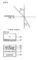
- FIG. 1is a diagram-for explaining the reduction in external quantum efficiency in a conventional vertical GaN-based LED.
- an incident angle ⁇ 1 at which photons are incident from a GaN layer to the airshould be less than a critical angle ⁇ c so that the photons generated from an active layer can pass through the GaN layer having a refractive index N 1 greater than a refractive index N 2 of the air and then escape into the air.
- the critical angle ⁇ csin ⁇ 1 (N 2 /N 1 ).
- a critical angleis about 23.6°.
- the incident angle ⁇ 1is greater than the critical angel ⁇ c , the photon is totally reflected at an interface between the GaN layer and the air and goes back into the LED. Then, the photon is confined inside the LED, so that the external quantum efficiency is greatly reduced.
- U.S Patent Publication No. 20030222263discloses that hemispherical convex patterns are formed on the surface of an n-type GaN layer to reduce an incident angle ⁇ 1 of photon incident to the air from the GaN layer below a critical angle ⁇ c .
- a method for manufacturing a vertical GaN-based LED disclosed in U.S. Patent Publication No. 20030222263will be described with reference to FIGS. 2 to 4 .
- FIGS. 2A to 2 Care sectional views illustrating a method of manufacturing the vertical GaN-based LED disclosed in U.S. Patent Publication No. 20030222263
- FIGS. 3A to 3 Care enlarged sectional views illustrating a method of manufacturing the vertical GaN-based LED
- FIG. 4is a sectional view of the vertical GaN-based LED manufactured through the method of FIGS. 2A to 2 C and FIGS. 3A to 3 C.
- an LED structure 16 including GaN and a positive electrode (p-electrode) 18are formed on a sapphire substrate 24 , and a first Pd layer 26 and an In layer 28 are formed on the p-electrode 18 . Further, a second Pd layer is formed under a silicon substrate 20 .
- the silicon substrate 20 where the second Pd layer 30 is formedis attached to the p-electrode 18 where the first Pd layer 26 and the In layer 28 are formed.
- the sapphire substrate 24is removed using an LLO process.
- photoresist patterns 32are formed on predetermined portions of the surface of the exposed LED structure 16 (more specifically, the surface of the n-type GaN layer) after the sapphire substrate 24 is removed.
- the photoresist patterns 32are formed in a hemispherical shape through a re-flow process.
- the surface of the LED structure 16is etched through an anisotropic etching process so as to be patterned in a hemispherical shape.
- a negative electrode (n-electrode) 34is formed on the LED structure 16 .
- the vertical GaN-based LED having the LED structure 16 whose surface is patternedis completed.
- the patterns for improving the external quantum efficiencyare formed in a convex hemispherical shape on the surface of the LED structure, the surface of the LED structure on which the patterns can be formed is limited. Accordingly, the improvement of the external quantum efficiency that can be achieved by applying the convex hemispherical patterns is not sufficient. Therefore, there is a demand for a new method that can maximize the improvement of the external quantum efficiency.
- An advantage of the present inventionis that it provides a method of manufacturing a vertical GaN-based LED, in which a p-type GaN layer is formed on a silicon substrate by using a nitride-based buffer layer without a separate doping process, and the surface of the p-type GaN layer is formed to have roughness through a wet etching process for removing the silicon substrate, the roughness being capable of scattering light. Therefore, the light extraction efficiency is enhanced, so that the external quantum efficiency can be improved, and simultaneously, an overall manufacturing process can be simplified.
- a method of manufacturing a vertical GaN-based LEDcomprises forming a nitride-based buffer layer on a silicon substrate; sequentially forming a p-type GaN layer, an active layer, and an n-type GaN layer on the nitride-based buffer layer; forming an n-electrode on the n-type GaN layer; forming a plating seed layer on the n-electrode; forming a structure supporting layer on the plating seed layer; removing the silicon substrate through wet etching and forming roughness on the surface of the p-type GaN layer through over-etching; and forming a p-electrode on the p-type GaN layer having the roughness formed.
- the nitride-based buffer layeris formed of AIN.
- the AINis formed at temperature of more than 1000° C.
- the p-type GaN layeris formed to have a thickness of ⁇ /4 of wavelength of light emitted in the active layer.
- the p-type GaN layeris formed to have a thickness of more than 500 nm.
- the wet-etching for removing the silicon substrateis performed by using a KOH solution as etching liquid.
- the methodfurther comprises forming a transparent conductive layer on the p-type GaN layer having the roughness formed, prior to the forming of the p-electrode.
- the transparent conductive layeris formed of CIO/ITO.
- the n-electrodeis formed of Ta/Ti/Al/Ni/Au or Al/Ti.
- the p-electrodeis formed of Ni/Au.
- the plating seed layeris formed of Cr/Au.
- the structure supporting layeris formed by electroplating or non-electroplating using any one selected from a group consisting of Ni, Au, and Cu.
- FIG. 1is a diagram for explaining the reduction in external quantum efficiency in a conventional vertical GaN-based LED
- FIGS. 2A to 2 Care sectional views illustrating a method of manufacturing the vertical GaN-based LED disclosed in U.S. Patent Publication No. 20030222263;
- FIGS. 3A to 3 Care enlarged sectional views illustrating a method of manufacturing the vertical GaN-based LED
- FIG. 4is a sectional view of the vertical GaN-based LED manufactured through the method of FIGS. 2A to 2 C and FIGS. 3A to 3 C
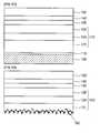
- FIGS. 5A to 5 Eare sectional views sequentially illustrating the method of manufacturing a vertical GaN-based LED according to an embodiment of the present invention
- FIG. 6is a graph showing a change in mobility and concentration of holes of the p-type GaN layer manufactured through the invention in accordance with heat treatment
- FIG. 7is a graph showing a voltage-current characteristic of an n-electrode in accordance with the p-type GaN layer manufactured through the invention.
- FIG. 8is a graph showing a voltage-current characteristic of a p-electrode in accordance with the p-type GaN layer manufactured through the invention.
- FIGS. 5A to 5 Eare sectional views sequentially illustrating the method of manufacturing a vertical GaN-based LED.
- an AIN buffer layer 110is formed on a silicon substrate 100 having an upper surface with a crystal direction ( 111 ) by using the MOCVD method through a nitride single crystal growth process.
- the AlN buffer layer 110is grown at temperature of more than 1000° C.
- a p-type GaN layer 121is formed on the AIN buffer layer 110 .
- the p-type GaN layer 121is formed to have a thickness of about ⁇ /4 (more than 500 nm) in order to secure a forming margin of roughness which is to be formed on the surface thereof through the following process.
- the p-type GaN layer 121is not formed by performing a separate p-type doping process on a GaN single crystal layer.
- the p-type GaN layer 121is formed when silicon (Si) atoms having an amphoteric characteristic act as an acceptor on a GaN layer with tensile strain, the silicon atoms being diffused from the silicon substrate 100 disposed under the p-type GaN layer 121 .
- the GaN layerhas a p-type characteristic (see Phys. Stat. Sol (c) No. 1, 425 ⁇ 429, 2002, Appl. Phys. Letters, Vol. 73, p 1188 ⁇ 1988).
- FIG. 6is a graph showing a change in mobility and concentration of holes of the p-type GaN layer manufactured thorugh the present invention in accordance with heat treatment.
- the concentration of ion having a p-type characteristichardly changes in accordance with a change in temperature of the heat treatment, and the mobility thereof hardly changes, as shown in FIG. 6 .
- the p-type GaN layeris manufactured according to the present invention, it is possible to omit a separate process of doping p-type ion and a heat treatment process of activating the p-type ion, thereby simplifying a manufacturing process.
- an active layer 124 and an n-type GaN layer 126are sequentially crystal-grown on the p-type GaN layer 121 so as to form a light-emitting structure 120 in which the p-type GaN layer 121 , the active layer 124 , and the n-type GaN layer 126 are sequentially laminated.
- an n-electrode 130is formed on the n-type GaN layer 126 .
- the n-electrode 130can serve as a reflective film.
- a separate reflective film(not shown) may be formed on the n-electrode 130 .
- the n-electrode 130is formed by using Ta/Ti/Al/Ni/Au or Al/Ti.
- the n-electrode 130is formed of Ta/Ti/Al/Ni/Au. Then, an n-electrode characteristic is verified in order to find a characteristic of the p-type GaN layer 121 manufactured according to the invention. As shown in FIG. 7 , it can be found that it normally shows a schottky characteristic.
- a structure supporting layer 150composed of a plating layer is formed on the plating seed layer 140 by performing electroplating or non-electroplating of Ni, Au, Cu or the like.
- the plating seed layer 130serves a crystal nucleus when the electroplating or non-electroplating is performed to form the structure supporting layer.
- the silicon substrate 100is removed by wet etching.
- the nitride-based buffer layer 110 positioned under the silicon substrate 100 and portions of the surface of the p-type GaN layerare also etched through over-etching.
- roughness 160which is capable of scattering light, is formed on the surface of the p-type GaN layer.
- the direction and structure of the roughness 160are determined by the crystal direction of the etched layer. Accordingly, the roughness 160 has a minute structure having a light scattering effect.
- the wet-etching process for obtaining preferable roughness 160can be performed at temperature of 75 to 100° C. by using etching liquid such as KOH.
- the roughness 160may be formed by performing wet etching using etching liquid such as KOH together with dry etching using ICP-RIE.
- a p-electrode 180is formed on the p-type GaN layer 121 having the roughness 160 formed. Then, an element separation process is performed through laser scribing, wet etching or dry etching. Alternately, the p-electrode 180 is formed after the element separation process, thereby forming a vertical GaN-based LED.
- the p-electrode 180is formed of Ni/Au. Then, characteristics of the p-electrode are verified in order to find out the characteristics of the p-type GaN layer 121 manufactured according to the invention. As a result, it can be found that the p-electrode normally shows an ohmic characteristic, as shown in FIG. 8 .
- a transparent conductive layer 170may be formed on the entire upper surface of the p-type GaN layer 121 by using CIO/ITO, before the p-electrode 180 is selectively formed.
- the p-type GaN layeris formed on the silicon substrate by using the nitride-based buffer layer without a separate doping process, and simultaneously, a heat treatment process for activating doping ion can be omitted, which makes it possible to simplify an overall manufacturing process.
- the roughness for scattering lightis easily formed on the surface of the p-type GaN layer without a separate photolithographic process, thereby enhancing the light extraction efficiency and maximizing an improved effect of external quantum efficiency.
- the characteristics and reliability of the vertical GaN-based LEDcan be enhanced, and simultaneously, an overall manufacturing process can be simplified, which makes it possible to increase production yield.
Landscapes
- Led Devices (AREA)
Abstract
Description
- The application claims the benefit of Korea Patent Application No. 2005-120599 filed with the Korea Intellectual Property Office on Dec. 9, 2005, the disclosure of which is incorporated herein by reference.
- 1. Field of the Invention
- The present invention relates to a method of manufacturing a vertical (vertical-electrode-type) GaN-based light emitting diode (LED), which is capable of increasing the light-extraction efficiency to enhance the external quantum efficiency and simultaneously simplifying an overall manufacturing process.
- 2. Description of the Related Art
- Generally, a GaN-based LED is grown on a sapphire substrate, but the sapphire substrate is a rigid nonconductor and has poor thermal conductivity. Therefore, there is a limitation in reducing the manufacturing costs by decreasing the size of a GaN-based LED, or improving the optical power and chip characteristic. Particularly, because the application of a high current is essential for achieving high power LED, it is important to solve a heat-sink problem of the LED. To solve this problem, there has been proposed a vertical GaN-based LED in which a sapphire substrate is removed using a laser lift-off (LLO).
- However, the conventional vertical GaN-based LED has a problem in that photon generated from an active layer is emitted to the outside of the LED. That is, the external quantum efficiency is degraded.
FIG. 1 is a diagram-for explaining the reduction in external quantum efficiency in a conventional vertical GaN-based LED. Referring toFIG. 1 , an incident angle θ1at which photons are incident from a GaN layer to the air should be less than a critical angle θcso that the photons generated from an active layer can pass through the GaN layer having a refractive index N1greater than a refractive index N2of the air and then escape into the air.- When an escape angle θ2at which the photon escapes into the air is 90°, the critical angle θcis defined as θc=sin−1(N2/N1). When light propagates from the GaN layer to the air having a refractive index of 1, a critical angle is about 23.6°.
- When the incident angle θ1is greater than the critical angel θc, the photon is totally reflected at an interface between the GaN layer and the air and goes back into the LED. Then, the photon is confined inside the LED, so that the external quantum efficiency is greatly reduced.
- To prevent the reduction in the external quantum efficiency, U.S Patent Publication No. 20030222263 discloses that hemispherical convex patterns are formed on the surface of an n-type GaN layer to reduce an incident angle θ1of photon incident to the air from the GaN layer below a critical angle θc.
- A method for manufacturing a vertical GaN-based LED disclosed in U.S. Patent Publication No. 20030222263 will be described with reference to FIGS.2 to4.
FIGS. 2A to2C are sectional views illustrating a method of manufacturing the vertical GaN-based LED disclosed in U.S. Patent Publication No. 20030222263,FIGS. 3A to3C are enlarged sectional views illustrating a method of manufacturing the vertical GaN-based LED, andFIG. 4 is a sectional view of the vertical GaN-based LED manufactured through the method ofFIGS. 2A to2C andFIGS. 3A to3C.- Referring to
FIG. 2A , anLED structure 16 including GaN and a positive electrode (p-electrode)18 are formed on asapphire substrate 24, and afirst Pd layer 26 and anIn layer 28 are formed on the p-electrode 18. Further, a second Pd layer is formed under asilicon substrate 20. - Referring to
FIG. 2B , thesilicon substrate 20 where thesecond Pd layer 30 is formed is attached to the p-electrode 18 where thefirst Pd layer 26 and theIn layer 28 are formed. - Referring to
FIG. 2C , thesapphire substrate 24 is removed using an LLO process. - Referring to
FIG. 3A ,photoresist patterns 32 are formed on predetermined portions of the surface of the exposed LED structure16 (more specifically, the surface of the n-type GaN layer) after thesapphire substrate 24 is removed. - Referring to
FIG. 3B , thephotoresist patterns 32 are formed in a hemispherical shape through a re-flow process. - Referring to
FIG. 3C , the surface of theLED structure 16 is etched through an anisotropic etching process so as to be patterned in a hemispherical shape. - Referring to
FIG. 4 , a negative electrode (n-electrode)34 is formed on theLED structure 16. Through these procedures, the vertical GaN-based LED having theLED structure 16 whose surface is patterned is completed. - However, according to the vertical GaN-based LED manufactured by the method disclosed in U.S. Patent Publication No. 20030222263, when the
LED structure 16 has a thickness of 10 μm or less (thin GaN), the process of forming thephotoresist patterns 32 and subsequent processes are difficult to carry out even if the silicon substrate acting as a sub support is used. Accordingly, the manufacturing yield significantly decreases. - In addition, because the patterns for improving the external quantum efficiency are formed in a convex hemispherical shape on the surface of the LED structure, the surface of the LED structure on which the patterns can be formed is limited. Accordingly, the improvement of the external quantum efficiency that can be achieved by applying the convex hemispherical patterns is not sufficient. Therefore, there is a demand for a new method that can maximize the improvement of the external quantum efficiency.
- An advantage of the present invention is that it provides a method of manufacturing a vertical GaN-based LED, in which a p-type GaN layer is formed on a silicon substrate by using a nitride-based buffer layer without a separate doping process, and the surface of the p-type GaN layer is formed to have roughness through a wet etching process for removing the silicon substrate, the roughness being capable of scattering light. Therefore, the light extraction efficiency is enhanced, so that the external quantum efficiency can be improved, and simultaneously, an overall manufacturing process can be simplified.
- Additional aspects and advantages of the present general inventive concept will be set forth in part in the description which follows and, in part, will be obvious from the description, or may be learned by practice of the general inventive concept.
- According to an aspect of the invention, a method of manufacturing a vertical GaN-based LED comprises forming a nitride-based buffer layer on a silicon substrate; sequentially forming a p-type GaN layer, an active layer, and an n-type GaN layer on the nitride-based buffer layer; forming an n-electrode on the n-type GaN layer; forming a plating seed layer on the n-electrode; forming a structure supporting layer on the plating seed layer; removing the silicon substrate through wet etching and forming roughness on the surface of the p-type GaN layer through over-etching; and forming a p-electrode on the p-type GaN layer having the roughness formed.
- According to another aspect of the invention, the nitride-based buffer layer is formed of AIN.
- According to a further aspect of the invention, the AIN is formed at temperature of more than 1000° C.
- According to a still further aspect of the invention, the p-type GaN layer is formed to have a thickness of λ/4 of wavelength of light emitted in the active layer.
- According to a still further aspect of the invention, the p-type GaN layer is formed to have a thickness of more than 500 nm.
- According to a still further aspect of the invention, the wet-etching for removing the silicon substrate is performed by using a KOH solution as etching liquid.
- According to a still further aspect of the invention, the method further comprises forming a transparent conductive layer on the p-type GaN layer having the roughness formed, prior to the forming of the p-electrode.
- According to a still further aspect of the invention, the transparent conductive layer is formed of CIO/ITO.
- According to a still further aspect of the invention, the n-electrode is formed of Ta/Ti/Al/Ni/Au or Al/Ti.
- According to a still further aspect of the invention, the p-electrode is formed of Ni/Au.
- According to a still further aspect of the invention, the plating seed layer is formed of Cr/Au.
- According to a still further aspect of the invention, the structure supporting layer is formed by electroplating or non-electroplating using any one selected from a group consisting of Ni, Au, and Cu.
- These and/or other aspects and advantages of the present general inventive concept will become apparent and more readily appreciated from the following description of the embodiments, taken in conjunction with the accompanying drawings of which:
FIG. 1 is a diagram for explaining the reduction in external quantum efficiency in a conventional vertical GaN-based LED;FIGS. 2A to2C are sectional views illustrating a method of manufacturing the vertical GaN-based LED disclosed in U.S. Patent Publication No. 20030222263;FIGS. 3A to3C are enlarged sectional views illustrating a method of manufacturing the vertical GaN-based LED;FIG. 4 is a sectional view of the vertical GaN-based LED manufactured through the method ofFIGS. 2A to2C andFIGS. 3A to3CFIGS. 5A to5E are sectional views sequentially illustrating the method of manufacturing a vertical GaN-based LED according to an embodiment of the present invention;FIG. 6 is a graph showing a change in mobility and concentration of holes of the p-type GaN layer manufactured through the invention in accordance with heat treatment;FIG. 7 is a graph showing a voltage-current characteristic of an n-electrode in accordance with the p-type GaN layer manufactured through the invention; andFIG. 8 is a graph showing a voltage-current characteristic of a p-electrode in accordance with the p-type GaN layer manufactured through the invention.- Reference will now be made in detail to the embodiments of the present general inventive concept, examples of which are illustrated in the accompanying drawings, wherein like reference numerals refer to the like elements throughout. The embodiments are described below in order to explain the present general inventive concept by referring to the figures.
- Hereinafter, a method of manufacturing a vertical GaN-based LED according to an embodiment of the invention will be described in detail with reference to the accompanying drawings.
- First, the method of manufacturing a vertical GaN-based LED will be described in detail with reference to
FIGS. 5A to5E. FIGS. 5A to5E are sectional views sequentially illustrating the method of manufacturing a vertical GaN-based LED.- Referring to
FIG. 5A , anAIN buffer layer 110 is formed on asilicon substrate 100 having an upper surface with a crystal direction (111) by using the MOCVD method through a nitride single crystal growth process. Preferably, theAlN buffer layer 110 is grown at temperature of more than 1000° C. - On the
AIN buffer layer 110, a p-type GaN layer 121 is formed. Preferably, the p-type GaN layer 121 is formed to have a thickness of about λ/4 (more than 500 nm) in order to secure a forming margin of roughness which is to be formed on the surface thereof through the following process. - The p-
type GaN layer 121 according to the invention is not formed by performing a separate p-type doping process on a GaN single crystal layer. At the time of growing GaN single crystal, the p-type GaN layer 121 is formed when silicon (Si) atoms having an amphoteric characteristic act as an acceptor on a GaN layer with tensile strain, the silicon atoms being diffused from thesilicon substrate 100 disposed under the p-type GaN layer 121. More specifically, when the silicon (Si) atoms diffused from thesilicon substrate 100 are combined with nitrogen (N) atoms of the GaN layer having tensile strain so as to form SiN and act as an acceptor, the GaN layer has a p-type characteristic (see Phys. Stat. Sol (c) No. 1, 425˜429, 2002, Appl. Phys. Letters, Vol. 73, p 1188˜1988). - When the p-
type GaN layer 121 is manufactured in such a manner, a heat treatment process may be omitted, which is performed so as to activate a doped p-type ion within a GaN layer.FIG. 6 is a graph showing a change in mobility and concentration of holes of the p-type GaN layer manufactured thorugh the present invention in accordance with heat treatment. In the p-type GaN layer 121 manufactured according to the invention, the concentration of ion having a p-type characteristic hardly changes in accordance with a change in temperature of the heat treatment, and the mobility thereof hardly changes, as shown inFIG. 6 . - Therefore, when the p-type GaN layer is manufactured according to the present invention, it is possible to omit a separate process of doping p-type ion and a heat treatment process of activating the p-type ion, thereby simplifying a manufacturing process.
- As shown in
FIG. 5B , anactive layer 124 and an n-type GaN layer 126 are sequentially crystal-grown on the p-type GaN layer 121 so as to form a light-emittingstructure 120 in which the p-type GaN layer 121, theactive layer 124, and the n-type GaN layer 126 are sequentially laminated. - As shown in
FIG. 5C , an n-electrode 130 is formed on the n-type GaN layer 126. At this time, the n-electrode 130 can serve as a reflective film. On the other hand, a separate reflective film (not shown) may be formed on the n-electrode 130. In this embodiment, the n-electrode 130 is formed by using Ta/Ti/Al/Ni/Au or Al/Ti. - In this embodiment, the n-
electrode 130 is formed of Ta/Ti/Al/Ni/Au. Then, an n-electrode characteristic is verified in order to find a characteristic of the p-type GaN layer 121 manufactured according to the invention. As shown inFIG. 7 , it can be found that it normally shows a schottky characteristic. - Next, after a
plating seed layer 140 is formed of Cr/Au on the n-electrode 130, astructure supporting layer 150 composed of a plating layer is formed on theplating seed layer 140 by performing electroplating or non-electroplating of Ni, Au, Cu or the like. At this time, theplating seed layer 130 serves a crystal nucleus when the electroplating or non-electroplating is performed to form the structure supporting layer. - Next, as shown in
FIG. 5D , thesilicon substrate 100 is removed by wet etching. In this case, the nitride-basedbuffer layer 110 positioned under thesilicon substrate 100 and portions of the surface of the p-type GaN layer are also etched through over-etching. Then,roughness 160, which is capable of scattering light, is formed on the surface of the p-type GaN layer. - At this time, the direction and structure of the
roughness 160 are determined by the crystal direction of the etched layer. Accordingly, theroughness 160 has a minute structure having a light scattering effect. The wet-etching process for obtainingpreferable roughness 160 can be performed at temperature of 75 to 100° C. by using etching liquid such as KOH. - The
roughness 160 may be formed by performing wet etching using etching liquid such as KOH together with dry etching using ICP-RIE. - Next, as shown in
FIG. 5E , a p-electrode 180 is formed on the p-type GaN layer 121 having theroughness 160 formed. Then, an element separation process is performed through laser scribing, wet etching or dry etching. Alternately, the p-electrode 180 is formed after the element separation process, thereby forming a vertical GaN-based LED. - In this embodiment, the p-
electrode 180 is formed of Ni/Au. Then, characteristics of the p-electrode are verified in order to find out the characteristics of the p-type GaN layer 121 manufactured according to the invention. As a result, it can be found that the p-electrode normally shows an ohmic characteristic, as shown inFIG. 8 . - In this embodiment, in order to enhance a current spreading effect, a transparent
conductive layer 170 may be formed on the entire upper surface of the p-type GaN layer 121 by using CIO/ITO, before the p-electrode 180 is selectively formed. - As described above, the p-type GaN layer is formed on the silicon substrate by using the nitride-based buffer layer without a separate doping process, and simultaneously, a heat treatment process for activating doping ion can be omitted, which makes it possible to simplify an overall manufacturing process.
- Further, the roughness for scattering light is easily formed on the surface of the p-type GaN layer without a separate photolithographic process, thereby enhancing the light extraction efficiency and maximizing an improved effect of external quantum efficiency.
- In the present invention, the characteristics and reliability of the vertical GaN-based LED can be enhanced, and simultaneously, an overall manufacturing process can be simplified, which makes it possible to increase production yield.
- Although a few embodiments of the present general inventive concept have been shown and described, it will be appreciated by those skilled in the art that changes may be made in these embodiments without departing from the principles and spirit of the general inventive concept, the scope of which is defined in the appended claims and their equivalents.
Claims (12)
Applications Claiming Priority (2)
| Application Number | Priority Date | Filing Date | Title |
|---|---|---|---|
| KR1020050120599AKR100661602B1 (en) | 2005-12-09 | 2005-12-09 | Method of manufacturing vertical structure gallium nitride based LED device |
| KR10-2005-0120599 | 2005-12-09 |
Publications (2)
| Publication Number | Publication Date |
|---|---|
| US20070134834A1true US20070134834A1 (en) | 2007-06-14 |
| US8361816B2 US8361816B2 (en) | 2013-01-29 |
Family
ID=37815629
Family Applications (1)
| Application Number | Title | Priority Date | Filing Date |
|---|---|---|---|
| US11/634,106Active2027-07-29US8361816B2 (en) | 2005-12-09 | 2006-12-06 | Method of manufacturing vertical gallium nitride based light emitting diode |
Country Status (2)
| Country | Link |
|---|---|
| US (1) | US8361816B2 (en) |
| KR (1) | KR100661602B1 (en) |
Cited By (35)
| Publication number | Priority date | Publication date | Assignee | Title |
|---|---|---|---|---|
| US20090072269A1 (en)* | 2007-09-17 | 2009-03-19 | Chang Soo Suh | Gallium nitride diodes and integrated components |
| US20090147813A1 (en)* | 2007-12-06 | 2009-06-11 | Kabushiki Kaisha Toshiba | Light-emitting device and method for producing light emitting device |
| US20090267078A1 (en)* | 2008-04-23 | 2009-10-29 | Transphorm Inc. | Enhancement Mode III-N HEMTs |
| US20100289067A1 (en)* | 2009-05-14 | 2010-11-18 | Transphorm Inc. | High Voltage III-Nitride Semiconductor Devices |
| US20110049526A1 (en)* | 2009-08-28 | 2011-03-03 | Transphorm Inc. | Semiconductor Devices with Field Plates |
| US20110121314A1 (en)* | 2007-09-17 | 2011-05-26 | Transphorm Inc. | Enhancement mode gallium nitride power devices |
| US20110127541A1 (en)* | 2008-12-10 | 2011-06-02 | Transphorm Inc. | Semiconductor heterostructure diodes |
| CN102087479A (en)* | 2009-12-02 | 2011-06-08 | 超科技公司 | Optical alignment methods for forming LEDs having a rough surface |
| US20110180828A1 (en)* | 2010-01-25 | 2011-07-28 | Micron Technology, Inc. | Solid state lighting devices and associated methods of manufacturing |
| US8289065B2 (en) | 2008-09-23 | 2012-10-16 | Transphorm Inc. | Inductive load power switching circuits |
| US8389977B2 (en) | 2009-12-10 | 2013-03-05 | Transphorm Inc. | Reverse side engineered III-nitride devices |
| US8598937B2 (en) | 2011-10-07 | 2013-12-03 | Transphorm Inc. | High power semiconductor electronic components with increased reliability |
| US8643062B2 (en) | 2011-02-02 | 2014-02-04 | Transphorm Inc. | III-N device structures and methods |
| US8716141B2 (en) | 2011-03-04 | 2014-05-06 | Transphorm Inc. | Electrode configurations for semiconductor devices |
| US8742460B2 (en) | 2010-12-15 | 2014-06-03 | Transphorm Inc. | Transistors with isolation regions |
| US8772842B2 (en) | 2011-03-04 | 2014-07-08 | Transphorm, Inc. | Semiconductor diodes with low reverse bias currents |
| US8901604B2 (en) | 2011-09-06 | 2014-12-02 | Transphorm Inc. | Semiconductor devices with guard rings |
| US9142741B2 (en) | 2011-06-15 | 2015-09-22 | Sensor Electronic Technology, Inc. | Emitting device with improved extraction |
| US9165766B2 (en) | 2012-02-03 | 2015-10-20 | Transphorm Inc. | Buffer layer structures suited for III-nitride devices with foreign substrates |
| US9171730B2 (en) | 2013-02-15 | 2015-10-27 | Transphorm Inc. | Electrodes for semiconductor devices and methods of forming the same |
| US9184275B2 (en) | 2012-06-27 | 2015-11-10 | Transphorm Inc. | Semiconductor devices with integrated hole collectors |
| US9257547B2 (en) | 2011-09-13 | 2016-02-09 | Transphorm Inc. | III-N device structures having a non-insulating substrate |
| US9287449B2 (en) | 2013-01-09 | 2016-03-15 | Sensor Electronic Technology, Inc. | Ultraviolet reflective rough adhesive contact |
| US20160093698A1 (en)* | 2014-09-26 | 2016-03-31 | Commissariat Á L'energie Atomique Et Aux Energies Alternatives | METHOD FOR DOPING A GaN-BASE SEMICONDUCTOR |
| US9337387B2 (en) | 2011-06-15 | 2016-05-10 | Sensor Electronic Technology, Inc. | Emitting device with improved extraction |
| US9478424B2 (en) | 2014-09-26 | 2016-10-25 | Commissariat à l'Energie Atomique et aux Energies Alternatives | Method for fabricating an improved GAN-based semiconductor layer |
| US9514962B2 (en) | 2014-09-26 | 2016-12-06 | Commissariat à l'Energie Atomique et aux Energies Alternatives | Method for performing activation of dopants in a GaN-base semiconductor layer |
| US9536741B2 (en) | 2014-09-26 | 2017-01-03 | Commissariat à l'Energie Atomique et aux Energies Alternatives | Method for performing activation of dopants in a GaN-base semiconductor layer by successive implantations and heat treatments |
| US9741899B2 (en) | 2011-06-15 | 2017-08-22 | Sensor Electronic Technology, Inc. | Device with inverted large scale light extraction structures |
| US9768357B2 (en) | 2013-01-09 | 2017-09-19 | Sensor Electronic Technology, Inc. | Ultraviolet reflective rough adhesive contact |
| US10276749B2 (en) | 2013-01-09 | 2019-04-30 | Sensor Electronic Technology, Inc. | Ultraviolet reflective rough adhesive contact |
| US10319881B2 (en) | 2011-06-15 | 2019-06-11 | Sensor Electronic Technology, Inc. | Device including transparent layer with profiled surface for improved extraction |
| US10461221B2 (en) | 2016-01-18 | 2019-10-29 | Sensor Electronic Technology, Inc. | Semiconductor device with improved light propagation |
| US10522714B2 (en) | 2011-06-15 | 2019-12-31 | Sensor Electronic Technology, Inc. | Device with inverted large scale light extraction structures |
| DE112012005156B4 (en) | 2011-12-07 | 2022-04-21 | OSRAM Opto Semiconductors Gesellschaft mit beschränkter Haftung | Optoelectronic semiconductor chip |
Families Citing this family (13)
| Publication number | Priority date | Publication date | Assignee | Title |
|---|---|---|---|---|
| US20100006884A1 (en)* | 2007-08-07 | 2010-01-14 | Epistar Corporation | Light Emitting Device and Manufacturing Method Therof |
| KR101199129B1 (en)* | 2009-12-21 | 2012-11-09 | 엘지이노텍 주식회사 | Semiconductor light emitting device and fabrication method thereof |
| WO2013155108A1 (en) | 2012-04-09 | 2013-10-17 | Transphorm Inc. | N-polar iii-nitride transistors |
| US9087718B2 (en) | 2013-03-13 | 2015-07-21 | Transphorm Inc. | Enhancement-mode III-nitride devices |
| US9245992B2 (en) | 2013-03-15 | 2016-01-26 | Transphorm Inc. | Carbon doping semiconductor devices |
| US9443938B2 (en) | 2013-07-19 | 2016-09-13 | Transphorm Inc. | III-nitride transistor including a p-type depleting layer |
| US9318593B2 (en) | 2014-07-21 | 2016-04-19 | Transphorm Inc. | Forming enhancement mode III-nitride devices |
| US9536967B2 (en) | 2014-12-16 | 2017-01-03 | Transphorm Inc. | Recessed ohmic contacts in a III-N device |
| US9536966B2 (en) | 2014-12-16 | 2017-01-03 | Transphorm Inc. | Gate structures for III-N devices |
| US11322599B2 (en) | 2016-01-15 | 2022-05-03 | Transphorm Technology, Inc. | Enhancement mode III-nitride devices having an Al1-xSixO gate insulator |
| TWI762486B (en) | 2016-05-31 | 2022-05-01 | 美商創世舫科技有限公司 | Iii-nitride devices including a graded depleting layer |
| CN119780471A (en)* | 2024-12-26 | 2025-04-08 | 南京邮电大学 | An optomechanical microcavity accelerometer based on quantum confined Stark effect and its preparation method |
| CN119780472A (en)* | 2024-12-26 | 2025-04-08 | 南京邮电大学 | A heterodyne optomechanical microcavity accelerometer based on quantum confined Stark effect and its preparation method |
Citations (50)
| Publication number | Priority date | Publication date | Assignee | Title |
|---|---|---|---|---|
| US5657335A (en)* | 1993-11-01 | 1997-08-12 | The Regents, University Of California | P-type gallium nitride |
| US5773369A (en)* | 1996-04-30 | 1998-06-30 | The Regents Of The University Of California | Photoelectrochemical wet etching of group III nitrides |
| US5792698A (en)* | 1993-12-09 | 1998-08-11 | Kabushiki Kaisha Toshiba | Method of manufacturing semiconductor light emitting device |
| US5877558A (en)* | 1993-04-28 | 1999-03-02 | Nichia Chemical Industries, Ltd. | Gallium nitride-based III-V group compound semiconductor |
| US5929466A (en)* | 1994-03-09 | 1999-07-27 | Kabushiki Kaisha Toshiba | Semiconductor device and method of fabricating the same |
| WO2000028536A1 (en)* | 1998-11-09 | 2000-05-18 | Seiko Instruments Inc. | Near-field optical head and production method thereof |
| US6270929B1 (en)* | 2000-07-20 | 2001-08-07 | Advanced Micro Devices, Inc. | Damascene T-gate using a relacs flow |
| US20020137236A1 (en)* | 2001-03-23 | 2002-09-26 | Schaff William J. | AIN coated heterojunction field effect transistor and method of forming an AIN coating |
| US20030180980A1 (en)* | 2001-12-21 | 2003-09-25 | Tal Margalith | Implantation for current confinement in nitride-based vertical optoelectronics |
| US20040137657A1 (en)* | 2001-03-30 | 2004-07-15 | Dmitriev Vladimir A. | Manufacturing methods for semiconductor devices with multiple III-V material layers |
| US20040169188A1 (en)* | 2000-09-22 | 2004-09-02 | Kabushiki Kaisha Toshiba | Optical device, surface emitting type device and method for manufacturing the same |
| US20040173816A1 (en)* | 2003-03-03 | 2004-09-09 | Saxler Adam William | Integrated nitride-based acoustic wave devices and methods of fabricating integrated nitride-based acoustic wave devices |
| US20040264533A1 (en)* | 2003-06-27 | 2004-12-30 | Hiroaki Matsumura | Nitride semiconductor laser device having current blocking layer and method of manufacturing the same |
| US20040266044A1 (en)* | 2003-06-24 | 2004-12-30 | Park Young Ho | Method for manufacturing gallium nitride-based semiconductor light emitting device |
| US20050007285A1 (en)* | 2002-01-22 | 2005-01-13 | Jean-Louis Oudar | Saturable absorber component and method for production of a saturable absorber component |
| US6884646B1 (en)* | 2004-03-10 | 2005-04-26 | Uni Light Technology Inc. | Method for forming an LED device with a metallic substrate |
| US20050167681A1 (en)* | 2004-02-04 | 2005-08-04 | Samsung Electronics Co., Ltd. | Electrode layer, light emitting device including the same, and method of forming the electrode layer |
| US20050247950A1 (en)* | 2004-05-06 | 2005-11-10 | Cree, Inc. | Lift-off process for GaN films formed on SiC substrates and devices fabricated using the method |
| WO2005106972A1 (en)* | 2004-04-29 | 2005-11-10 | Osram Opto Semiconductors Gmbh | Method for production a radiation-emitting semi-conductor chip |
| US7009218B2 (en)* | 2003-02-19 | 2006-03-07 | Nichia Corporation | Nitride semiconductor device |
| US20060126694A1 (en)* | 2004-12-14 | 2006-06-15 | Kwon O Kyun | Hybrid metal bonded vertical cavity surface emitting laser and fabricating method thereof |
| US20060154390A1 (en)* | 2005-01-11 | 2006-07-13 | Tran Chuong A | Systems and methods for producing light emitting diode array |
| US20060154455A1 (en)* | 2002-12-04 | 2006-07-13 | Emcore Corporation | Gallium nitride-based devices and manufacturing process |
| US20060175701A1 (en)* | 2005-02-04 | 2006-08-10 | Harald Gross | Dissociated fabrication of packages and chips of integrated circuits |
| US20060189123A1 (en)* | 2003-09-04 | 2006-08-24 | Advanced Display Inc. | Etchant and method of etching |
| US7105850B2 (en)* | 2004-08-04 | 2006-09-12 | Formosa Epitaxy Incorporation | GaN LED structure with p-type contacting layer grown at low-temperature and having low resistivity |
| US20060223313A1 (en)* | 2005-04-01 | 2006-10-05 | Agency For Science, Technology And Research | Copper interconnect post for connecting a semiconductor chip to a substrate and method of fabricating the same |
| US20060255341A1 (en)* | 2005-04-21 | 2006-11-16 | Aonex Technologies, Inc. | Bonded intermediate substrate and method of making same |
| US20060256825A1 (en)* | 2003-07-10 | 2006-11-16 | Nichia Corporation | Nitride semiconductor laser element |
| US20060267152A1 (en)* | 2003-08-05 | 2006-11-30 | Micron Technology, Inc. | Strained Si/SiGe/SOI islands and processes of making same |
| US20070018187A1 (en)* | 2005-07-22 | 2007-01-25 | Samsung Electro-Mechanics Co., Ltd. | Vertical GaN-based LED and method of manfacturing the same |
| US20070121690A1 (en)* | 2003-12-09 | 2007-05-31 | Tetsuo Fujii | Highly efficient gallium nitride based light emitting diodes via surface roughening |
| US20070148923A1 (en)* | 2004-07-09 | 2007-06-28 | Samsung Electro-Mechanics Co., Ltd. | Nitride semiconductor device and method of manufacturing the same |
| US20070205087A1 (en)* | 2004-04-12 | 2007-09-06 | Pashby Gary J | Single-Pole Double-Throw Mems Switch |
| US20070221944A1 (en)* | 2005-11-15 | 2007-09-27 | Myung Cheol Yoo | Light emitting diodes and fabrication methods thereof |
| US20070238314A1 (en)* | 2003-08-04 | 2007-10-11 | Nanosys, Inc. | System and process for producing nanowire composites and electronic substrates therefrom |
| US20070264805A1 (en)* | 2004-12-30 | 2007-11-15 | Finisar Corporation | Integrated light emitting device and photodiode with ohmic contact |
| US20080017868A1 (en)* | 2003-10-14 | 2008-01-24 | Nichia Corporation | Semiconductor laser having protruding portion |
| US20080035936A1 (en)* | 2006-08-14 | 2008-02-14 | Lester Steven D | GaN based LED with improved light extraction efficiency and method for making the same |
| US20080089383A1 (en)* | 2003-06-06 | 2008-04-17 | Chang Liu | Microfabricated temperature sensor |
| US20080135868A1 (en)* | 2004-10-01 | 2008-06-12 | Mitsubishi Cable Industries, Ltd. | Nitride Semiconductor Light Emitting Element and Method for Manufacturing the Same |
| US20080194050A1 (en)* | 2005-02-14 | 2008-08-14 | Kabushiki Kaisha Toshiba | Semiconductor light-emitting element and light-emitting device |
| US20080224154A1 (en)* | 2005-10-27 | 2008-09-18 | Lattice Power (Jiangxi) Corporation | Semiconductor Light-Emitting Device With Metal Support Substrate |
| US20090121657A1 (en)* | 2003-12-12 | 2009-05-14 | Luminus Devices, Inc. | Optical display systems and methods |
| US20090121242A1 (en)* | 2005-07-06 | 2009-05-14 | Showa Denko K.K. | Compound semiconductor light-emitting diode and method for fabrication thereof |
| US20090130787A1 (en)* | 2002-09-30 | 2009-05-21 | Osram Gmbh | Method for fabricating a plurality of electromagnetic radiation emitting semiconductor chips |
| US20090174035A1 (en)* | 2005-09-12 | 2009-07-09 | Sanyo Electric Co., Ltd. | Semiconductor Device |
| US20090189192A1 (en)* | 2006-07-27 | 2009-07-30 | Ruben Lieten | DEPOSITION OF GROUP III-NITRIDES ON Ge |
| US20090291313A1 (en)* | 2005-10-21 | 2009-11-26 | Wisconsin Alummi Research Foundation | Microelectronics grade metal substrate, related metal-embedded devices and methods for fabricating same |
| US20090289330A1 (en)* | 2003-10-17 | 2009-11-26 | Hitachi Cable, Ltd. | Group iii nitride semiconductor substrate, substrate for group iii nitride semiconductor device, and methods of making same |
Family Cites Families (3)
| Publication number | Priority date | Publication date | Assignee | Title |
|---|---|---|---|---|
| JP2001298210A (en)* | 2000-04-11 | 2001-10-26 | Nippon Telegr & Teleph Corp <Ntt> | Semiconductor light receiving element |
| US6391748B1 (en)* | 2000-10-03 | 2002-05-21 | Texas Tech University | Method of epitaxial growth of high quality nitride layers on silicon substrates |
| US20030222263A1 (en) | 2002-06-04 | 2003-12-04 | Kopin Corporation | High-efficiency light-emitting diodes |
- 2005
- 2005-12-09KRKR1020050120599Apatent/KR100661602B1/enactiveActive
- 2006
- 2006-12-06USUS11/634,106patent/US8361816B2/enactiveActive
Patent Citations (52)
| Publication number | Priority date | Publication date | Assignee | Title |
|---|---|---|---|---|
| US5877558A (en)* | 1993-04-28 | 1999-03-02 | Nichia Chemical Industries, Ltd. | Gallium nitride-based III-V group compound semiconductor |
| US5657335A (en)* | 1993-11-01 | 1997-08-12 | The Regents, University Of California | P-type gallium nitride |
| US5792698A (en)* | 1993-12-09 | 1998-08-11 | Kabushiki Kaisha Toshiba | Method of manufacturing semiconductor light emitting device |
| US5929466A (en)* | 1994-03-09 | 1999-07-27 | Kabushiki Kaisha Toshiba | Semiconductor device and method of fabricating the same |
| US5773369A (en)* | 1996-04-30 | 1998-06-30 | The Regents Of The University Of California | Photoelectrochemical wet etching of group III nitrides |
| US7599277B1 (en)* | 1998-11-09 | 2009-10-06 | Seiko Instruments Inc. | Near-field optical head having tapered hole for guiding light beam |
| WO2000028536A1 (en)* | 1998-11-09 | 2000-05-18 | Seiko Instruments Inc. | Near-field optical head and production method thereof |
| US6270929B1 (en)* | 2000-07-20 | 2001-08-07 | Advanced Micro Devices, Inc. | Damascene T-gate using a relacs flow |
| US20040169188A1 (en)* | 2000-09-22 | 2004-09-02 | Kabushiki Kaisha Toshiba | Optical device, surface emitting type device and method for manufacturing the same |
| US20020137236A1 (en)* | 2001-03-23 | 2002-09-26 | Schaff William J. | AIN coated heterojunction field effect transistor and method of forming an AIN coating |
| US20040137657A1 (en)* | 2001-03-30 | 2004-07-15 | Dmitriev Vladimir A. | Manufacturing methods for semiconductor devices with multiple III-V material layers |
| US20030180980A1 (en)* | 2001-12-21 | 2003-09-25 | Tal Margalith | Implantation for current confinement in nitride-based vertical optoelectronics |
| US20050007285A1 (en)* | 2002-01-22 | 2005-01-13 | Jean-Louis Oudar | Saturable absorber component and method for production of a saturable absorber component |
| US20090130787A1 (en)* | 2002-09-30 | 2009-05-21 | Osram Gmbh | Method for fabricating a plurality of electromagnetic radiation emitting semiconductor chips |
| US20060154455A1 (en)* | 2002-12-04 | 2006-07-13 | Emcore Corporation | Gallium nitride-based devices and manufacturing process |
| US7009218B2 (en)* | 2003-02-19 | 2006-03-07 | Nichia Corporation | Nitride semiconductor device |
| US20040173816A1 (en)* | 2003-03-03 | 2004-09-09 | Saxler Adam William | Integrated nitride-based acoustic wave devices and methods of fabricating integrated nitride-based acoustic wave devices |
| US20080089383A1 (en)* | 2003-06-06 | 2008-04-17 | Chang Liu | Microfabricated temperature sensor |
| US20040266044A1 (en)* | 2003-06-24 | 2004-12-30 | Park Young Ho | Method for manufacturing gallium nitride-based semiconductor light emitting device |
| US20040264533A1 (en)* | 2003-06-27 | 2004-12-30 | Hiroaki Matsumura | Nitride semiconductor laser device having current blocking layer and method of manufacturing the same |
| US20060256825A1 (en)* | 2003-07-10 | 2006-11-16 | Nichia Corporation | Nitride semiconductor laser element |
| US20070238314A1 (en)* | 2003-08-04 | 2007-10-11 | Nanosys, Inc. | System and process for producing nanowire composites and electronic substrates therefrom |
| US20060267152A1 (en)* | 2003-08-05 | 2006-11-30 | Micron Technology, Inc. | Strained Si/SiGe/SOI islands and processes of making same |
| US20060189123A1 (en)* | 2003-09-04 | 2006-08-24 | Advanced Display Inc. | Etchant and method of etching |
| US20080017868A1 (en)* | 2003-10-14 | 2008-01-24 | Nichia Corporation | Semiconductor laser having protruding portion |
| US20090289330A1 (en)* | 2003-10-17 | 2009-11-26 | Hitachi Cable, Ltd. | Group iii nitride semiconductor substrate, substrate for group iii nitride semiconductor device, and methods of making same |
| US20070121690A1 (en)* | 2003-12-09 | 2007-05-31 | Tetsuo Fujii | Highly efficient gallium nitride based light emitting diodes via surface roughening |
| US20090121657A1 (en)* | 2003-12-12 | 2009-05-14 | Luminus Devices, Inc. | Optical display systems and methods |
| US20050167681A1 (en)* | 2004-02-04 | 2005-08-04 | Samsung Electronics Co., Ltd. | Electrode layer, light emitting device including the same, and method of forming the electrode layer |
| US6884646B1 (en)* | 2004-03-10 | 2005-04-26 | Uni Light Technology Inc. | Method for forming an LED device with a metallic substrate |
| US20070205087A1 (en)* | 2004-04-12 | 2007-09-06 | Pashby Gary J | Single-Pole Double-Throw Mems Switch |
| US20080093611A1 (en)* | 2004-04-29 | 2008-04-24 | Berthold Hahn | Method for Production of a Radiation-Emitting Semiconductor Chip |
| WO2005106972A1 (en)* | 2004-04-29 | 2005-11-10 | Osram Opto Semiconductors Gmbh | Method for production a radiation-emitting semi-conductor chip |
| US20050247950A1 (en)* | 2004-05-06 | 2005-11-10 | Cree, Inc. | Lift-off process for GaN films formed on SiC substrates and devices fabricated using the method |
| US20070148923A1 (en)* | 2004-07-09 | 2007-06-28 | Samsung Electro-Mechanics Co., Ltd. | Nitride semiconductor device and method of manufacturing the same |
| US7105850B2 (en)* | 2004-08-04 | 2006-09-12 | Formosa Epitaxy Incorporation | GaN LED structure with p-type contacting layer grown at low-temperature and having low resistivity |
| US20080135868A1 (en)* | 2004-10-01 | 2008-06-12 | Mitsubishi Cable Industries, Ltd. | Nitride Semiconductor Light Emitting Element and Method for Manufacturing the Same |
| US20060126694A1 (en)* | 2004-12-14 | 2006-06-15 | Kwon O Kyun | Hybrid metal bonded vertical cavity surface emitting laser and fabricating method thereof |
| US20070264805A1 (en)* | 2004-12-30 | 2007-11-15 | Finisar Corporation | Integrated light emitting device and photodiode with ohmic contact |
| US20060154390A1 (en)* | 2005-01-11 | 2006-07-13 | Tran Chuong A | Systems and methods for producing light emitting diode array |
| US20060175701A1 (en)* | 2005-02-04 | 2006-08-10 | Harald Gross | Dissociated fabrication of packages and chips of integrated circuits |
| US20080194050A1 (en)* | 2005-02-14 | 2008-08-14 | Kabushiki Kaisha Toshiba | Semiconductor light-emitting element and light-emitting device |
| US20060223313A1 (en)* | 2005-04-01 | 2006-10-05 | Agency For Science, Technology And Research | Copper interconnect post for connecting a semiconductor chip to a substrate and method of fabricating the same |
| US20060255341A1 (en)* | 2005-04-21 | 2006-11-16 | Aonex Technologies, Inc. | Bonded intermediate substrate and method of making same |
| US20090121242A1 (en)* | 2005-07-06 | 2009-05-14 | Showa Denko K.K. | Compound semiconductor light-emitting diode and method for fabrication thereof |
| US20070018187A1 (en)* | 2005-07-22 | 2007-01-25 | Samsung Electro-Mechanics Co., Ltd. | Vertical GaN-based LED and method of manfacturing the same |
| US20090174035A1 (en)* | 2005-09-12 | 2009-07-09 | Sanyo Electric Co., Ltd. | Semiconductor Device |
| US20090291313A1 (en)* | 2005-10-21 | 2009-11-26 | Wisconsin Alummi Research Foundation | Microelectronics grade metal substrate, related metal-embedded devices and methods for fabricating same |
| US20080224154A1 (en)* | 2005-10-27 | 2008-09-18 | Lattice Power (Jiangxi) Corporation | Semiconductor Light-Emitting Device With Metal Support Substrate |
| US20070221944A1 (en)* | 2005-11-15 | 2007-09-27 | Myung Cheol Yoo | Light emitting diodes and fabrication methods thereof |
| US20090189192A1 (en)* | 2006-07-27 | 2009-07-30 | Ruben Lieten | DEPOSITION OF GROUP III-NITRIDES ON Ge |
| US20080035936A1 (en)* | 2006-08-14 | 2008-02-14 | Lester Steven D | GaN based LED with improved light extraction efficiency and method for making the same |
Non-Patent Citations (1)
| Title |
|---|
| Kim et al. "Investigate of Ta/Ti/Al/Ni/Au ohmic contact to AlGaN/GaN heterostructure field-effect transistor" J. Vac. Sci Technol. B 23(1), January 26, 2005* |
Cited By (81)
| Publication number | Priority date | Publication date | Assignee | Title |
|---|---|---|---|---|
| US9343560B2 (en) | 2007-09-17 | 2016-05-17 | Transphorm Inc. | Gallium nitride power devices |
| US8344424B2 (en) | 2007-09-17 | 2013-01-01 | Transphorm Inc. | Enhancement mode gallium nitride power devices |
| US20090072269A1 (en)* | 2007-09-17 | 2009-03-19 | Chang Soo Suh | Gallium nitride diodes and integrated components |
| US20110121314A1 (en)* | 2007-09-17 | 2011-05-26 | Transphorm Inc. | Enhancement mode gallium nitride power devices |
| US8633518B2 (en) | 2007-09-17 | 2014-01-21 | Transphorm Inc. | Gallium nitride power devices |
| US8193562B2 (en) | 2007-09-17 | 2012-06-05 | Tansphorm Inc. | Enhancement mode gallium nitride power devices |
| US20090147813A1 (en)* | 2007-12-06 | 2009-06-11 | Kabushiki Kaisha Toshiba | Light-emitting device and method for producing light emitting device |
| US8361822B2 (en) | 2007-12-06 | 2013-01-29 | Kabushiki Kaisha Toshiba | Light-emitting device and method for producing light emitting device |
| US8148714B2 (en) | 2007-12-06 | 2012-04-03 | Kabushiki Kaisha Toshiba | Light-emitting device and method for producing light emitting device |
| US8076168B2 (en)* | 2007-12-06 | 2011-12-13 | Kabushiki Kaisha Toshiba | Light-emitting device and method for producing light emitting device |
| US9941399B2 (en) | 2008-04-23 | 2018-04-10 | Transphorm Inc. | Enhancement mode III-N HEMTs |
| US9437708B2 (en) | 2008-04-23 | 2016-09-06 | Transphorm Inc. | Enhancement mode III-N HEMTs |
| US8519438B2 (en) | 2008-04-23 | 2013-08-27 | Transphorm Inc. | Enhancement mode III-N HEMTs |
| US8841702B2 (en) | 2008-04-23 | 2014-09-23 | Transphorm Inc. | Enhancement mode III-N HEMTs |
| US9196716B2 (en) | 2008-04-23 | 2015-11-24 | Transphorm Inc. | Enhancement mode III-N HEMTs |
| US20090267078A1 (en)* | 2008-04-23 | 2009-10-29 | Transphorm Inc. | Enhancement Mode III-N HEMTs |
| US9690314B2 (en) | 2008-09-23 | 2017-06-27 | Transphorm Inc. | Inductive load power switching circuits |
| US8289065B2 (en) | 2008-09-23 | 2012-10-16 | Transphorm Inc. | Inductive load power switching circuits |
| US8493129B2 (en) | 2008-09-23 | 2013-07-23 | Transphorm Inc. | Inductive load power switching circuits |
| US8531232B2 (en) | 2008-09-23 | 2013-09-10 | Transphorm Inc. | Inductive load power switching circuits |
| US8816751B2 (en) | 2008-09-23 | 2014-08-26 | Transphorm Inc. | Inductive load power switching circuits |
| US8237198B2 (en) | 2008-12-10 | 2012-08-07 | Transphorm Inc. | Semiconductor heterostructure diodes |
| US8541818B2 (en) | 2008-12-10 | 2013-09-24 | Transphorm Inc. | Semiconductor heterostructure diodes |
| US9041065B2 (en) | 2008-12-10 | 2015-05-26 | Transphorm Inc. | Semiconductor heterostructure diodes |
| US20110127541A1 (en)* | 2008-12-10 | 2011-06-02 | Transphorm Inc. | Semiconductor heterostructure diodes |
| US9293561B2 (en) | 2009-05-14 | 2016-03-22 | Transphorm Inc. | High voltage III-nitride semiconductor devices |
| US8742459B2 (en)* | 2009-05-14 | 2014-06-03 | Transphorm Inc. | High voltage III-nitride semiconductor devices |
| US20100289067A1 (en)* | 2009-05-14 | 2010-11-18 | Transphorm Inc. | High Voltage III-Nitride Semiconductor Devices |
| US9111961B2 (en) | 2009-08-28 | 2015-08-18 | Transphorm Inc. | Semiconductor devices with field plates |
| US20110049526A1 (en)* | 2009-08-28 | 2011-03-03 | Transphorm Inc. | Semiconductor Devices with Field Plates |
| US9373699B2 (en) | 2009-08-28 | 2016-06-21 | Transphorm Inc. | Semiconductor devices with field plates |
| US8390000B2 (en) | 2009-08-28 | 2013-03-05 | Transphorm Inc. | Semiconductor devices with field plates |
| US8692294B2 (en) | 2009-08-28 | 2014-04-08 | Transphorm Inc. | Semiconductor devices with field plates |
| US9831315B2 (en) | 2009-08-28 | 2017-11-28 | Transphorm Inc. | Semiconductor devices with field plates |
| US8781213B2 (en) | 2009-12-02 | 2014-07-15 | Ultratech, Inc. | Optical alignment systems for forming LEDs having a rough surface |
| CN102087479A (en)* | 2009-12-02 | 2011-06-08 | 超科技公司 | Optical alignment methods for forming LEDs having a rough surface |
| US8389977B2 (en) | 2009-12-10 | 2013-03-05 | Transphorm Inc. | Reverse side engineered III-nitride devices |
| US9496137B2 (en) | 2009-12-10 | 2016-11-15 | Transphorm Inc. | Methods of forming reverse side engineered III-nitride devices |
| US10199217B2 (en) | 2009-12-10 | 2019-02-05 | Transphorm Inc. | Methods of forming reverse side engineered III-nitride devices |
| US20110180828A1 (en)* | 2010-01-25 | 2011-07-28 | Micron Technology, Inc. | Solid state lighting devices and associated methods of manufacturing |
| US8709846B2 (en) | 2010-01-25 | 2014-04-29 | Micron Technology, Inc. | Solid state lighting devices and associated methods of manufacturing |
| US8476640B2 (en) | 2010-01-25 | 2013-07-02 | Micron Technology, Inc. | Solid state lighting devices and associated methods of manufacturing |
| US8129205B2 (en) | 2010-01-25 | 2012-03-06 | Micron Technology, Inc. | Solid state lighting devices and associated methods of manufacturing |
| US8742460B2 (en) | 2010-12-15 | 2014-06-03 | Transphorm Inc. | Transistors with isolation regions |
| US9147760B2 (en) | 2010-12-15 | 2015-09-29 | Transphorm Inc. | Transistors with isolation regions |
| US9437707B2 (en) | 2010-12-15 | 2016-09-06 | Transphorm Inc. | Transistors with isolation regions |
| US8643062B2 (en) | 2011-02-02 | 2014-02-04 | Transphorm Inc. | III-N device structures and methods |
| US8895421B2 (en) | 2011-02-02 | 2014-11-25 | Transphorm Inc. | III-N device structures and methods |
| US9224671B2 (en) | 2011-02-02 | 2015-12-29 | Transphorm Inc. | III-N device structures and methods |
| US8772842B2 (en) | 2011-03-04 | 2014-07-08 | Transphorm, Inc. | Semiconductor diodes with low reverse bias currents |
| US9142659B2 (en) | 2011-03-04 | 2015-09-22 | Transphorm Inc. | Electrode configurations for semiconductor devices |
| US8895423B2 (en) | 2011-03-04 | 2014-11-25 | Transphorm Inc. | Method for making semiconductor diodes with low reverse bias currents |
| US8716141B2 (en) | 2011-03-04 | 2014-05-06 | Transphorm Inc. | Electrode configurations for semiconductor devices |
| US9337387B2 (en) | 2011-06-15 | 2016-05-10 | Sensor Electronic Technology, Inc. | Emitting device with improved extraction |
| US9741899B2 (en) | 2011-06-15 | 2017-08-22 | Sensor Electronic Technology, Inc. | Device with inverted large scale light extraction structures |
| US10522714B2 (en) | 2011-06-15 | 2019-12-31 | Sensor Electronic Technology, Inc. | Device with inverted large scale light extraction structures |
| US9911900B2 (en) | 2011-06-15 | 2018-03-06 | Sensor Electronic Technology, Inc. | Device including transparent layer with profiled surface for improved extraction |
| US10319881B2 (en) | 2011-06-15 | 2019-06-11 | Sensor Electronic Technology, Inc. | Device including transparent layer with profiled surface for improved extraction |
| US9142741B2 (en) | 2011-06-15 | 2015-09-22 | Sensor Electronic Technology, Inc. | Emitting device with improved extraction |
| US8901604B2 (en) | 2011-09-06 | 2014-12-02 | Transphorm Inc. | Semiconductor devices with guard rings |
| US9224805B2 (en) | 2011-09-06 | 2015-12-29 | Transphorm Inc. | Semiconductor devices with guard rings |
| US9257547B2 (en) | 2011-09-13 | 2016-02-09 | Transphorm Inc. | III-N device structures having a non-insulating substrate |
| US8598937B2 (en) | 2011-10-07 | 2013-12-03 | Transphorm Inc. | High power semiconductor electronic components with increased reliability |
| US9171836B2 (en) | 2011-10-07 | 2015-10-27 | Transphorm Inc. | Method of forming electronic components with increased reliability |
| US8860495B2 (en) | 2011-10-07 | 2014-10-14 | Transphorm Inc. | Method of forming electronic components with increased reliability |
| DE112012005156B4 (en) | 2011-12-07 | 2022-04-21 | OSRAM Opto Semiconductors Gesellschaft mit beschränkter Haftung | Optoelectronic semiconductor chip |
| US9165766B2 (en) | 2012-02-03 | 2015-10-20 | Transphorm Inc. | Buffer layer structures suited for III-nitride devices with foreign substrates |
| US9685323B2 (en) | 2012-02-03 | 2017-06-20 | Transphorm Inc. | Buffer layer structures suited for III-nitride devices with foreign substrates |
| US9634100B2 (en) | 2012-06-27 | 2017-04-25 | Transphorm Inc. | Semiconductor devices with integrated hole collectors |
| US9184275B2 (en) | 2012-06-27 | 2015-11-10 | Transphorm Inc. | Semiconductor devices with integrated hole collectors |
| US10276749B2 (en) | 2013-01-09 | 2019-04-30 | Sensor Electronic Technology, Inc. | Ultraviolet reflective rough adhesive contact |
| US9287449B2 (en) | 2013-01-09 | 2016-03-15 | Sensor Electronic Technology, Inc. | Ultraviolet reflective rough adhesive contact |
| US9768357B2 (en) | 2013-01-09 | 2017-09-19 | Sensor Electronic Technology, Inc. | Ultraviolet reflective rough adhesive contact |
| US9171730B2 (en) | 2013-02-15 | 2015-10-27 | Transphorm Inc. | Electrodes for semiconductor devices and methods of forming the same |
| US9520491B2 (en) | 2013-02-15 | 2016-12-13 | Transphorm Inc. | Electrodes for semiconductor devices and methods of forming the same |
| US9536741B2 (en) | 2014-09-26 | 2017-01-03 | Commissariat à l'Energie Atomique et aux Energies Alternatives | Method for performing activation of dopants in a GaN-base semiconductor layer by successive implantations and heat treatments |
| US9514962B2 (en) | 2014-09-26 | 2016-12-06 | Commissariat à l'Energie Atomique et aux Energies Alternatives | Method for performing activation of dopants in a GaN-base semiconductor layer |
| US9496348B2 (en)* | 2014-09-26 | 2016-11-15 | Commissariat à l'Energie Atomique et aux Energies Alternatives | Method for doping a GaN-base semiconductor |
| US9478424B2 (en) | 2014-09-26 | 2016-10-25 | Commissariat à l'Energie Atomique et aux Energies Alternatives | Method for fabricating an improved GAN-based semiconductor layer |
| US20160093698A1 (en)* | 2014-09-26 | 2016-03-31 | Commissariat Á L'energie Atomique Et Aux Energies Alternatives | METHOD FOR DOPING A GaN-BASE SEMICONDUCTOR |
| US10461221B2 (en) | 2016-01-18 | 2019-10-29 | Sensor Electronic Technology, Inc. | Semiconductor device with improved light propagation |
Also Published As
| Publication number | Publication date |
|---|---|
| KR100661602B1 (en) | 2006-12-26 |
| US8361816B2 (en) | 2013-01-29 |
Similar Documents
| Publication | Publication Date | Title |
|---|---|---|
| US8361816B2 (en) | Method of manufacturing vertical gallium nitride based light emitting diode | |
| KR100631981B1 (en) | Vertical group III-nitride light emitting device and method of manufacturing the same | |
| JP4939099B2 (en) | Method for manufacturing vertical structure group 3 nitride light emitting device | |
| US7436001B2 (en) | Vertical GaN-based LED and method of manufacturing the same | |
| JP4766966B2 (en) | Light emitting element | |
| JP4996706B2 (en) | Semiconductor light emitting device and manufacturing method thereof | |
| CN101026213B (en) | Light emitting device and method of manufacturing the same | |
| JP5165276B2 (en) | Vertical structure gallium nitride based light-emitting diode device and method of manufacturing the same | |
| JP4786430B2 (en) | Manufacturing method of light emitting diode | |
| US6781147B2 (en) | Lateral current blocking light emitting diode and method of making the same | |
| US9741897B2 (en) | Thin light emitting diode and fabrication method | |
| US20130009167A1 (en) | Light emitting diode with patterned structures and method of making the same | |
| JP2004193619A (en) | Light-emitting device with enhanced light scattering | |
| TW201719931A (en) | Optoelectronic component | |
| US20150372192A1 (en) | Method and apparatus for creating a porus reflective contact | |
| TW201121092A (en) | Method of forming vertical structure light emitting diode with heat exhaustion structure | |
| CN102097561A (en) | Semi-conductor light emitting device and method for manufacturing thereof | |
| US7135713B2 (en) | Light emitting diode and method for manufacturing the same | |
| TW201034238A (en) | Semiconductor optoelectronic device with enhanced light extraction efficiency and fabricating method thereof | |
| JP5165668B2 (en) | Semiconductor light emitting device and manufacturing method thereof | |
| US20100224900A1 (en) | Semiconductor optoelectronic device and method for making the same | |
| CN107591463B (en) | Light emitting module and method for manufacturing light emitting module | |
| Lee et al. | Fabricating GaN-based LEDs with V-shape sapphire facet mirror by double transferred scheme |
Legal Events
| Date | Code | Title | Description |
|---|---|---|---|
| AS | Assignment | Owner name:SAMSUNG ELECTRO-MECHANICS CO., LTD., KOREA, REPUBL Free format text:ASSIGNMENT OF ASSIGNORS INTEREST;ASSIGNORS:LEE, JAE HOON;LEE, JUNG HEE;CHO, HYUN ICK;AND OTHERS;REEL/FRAME:018680/0456;SIGNING DATES FROM 20060904 TO 20061011 Owner name:SAMSUNG ELECTRO-MECHANICS CO., LTD., KOREA, REPUBL Free format text:ASSIGNMENT OF ASSIGNORS INTEREST;ASSIGNORS:LEE, JAE HOON;LEE, JUNG HEE;CHO, HYUN ICK;AND OTHERS;SIGNING DATES FROM 20060904 TO 20061011;REEL/FRAME:018680/0456 | |
| AS | Assignment | Owner name:SAMSUNG LED CO., LTD.,KOREA, REPUBLIC OF Free format text:ASSIGNMENT OF ASSIGNORS INTEREST;ASSIGNOR:SAMSUNG ELECTRO-MECHANICS CO., LTD.;REEL/FRAME:024375/0448 Effective date:20100511 Owner name:SAMSUNG LED CO., LTD., KOREA, REPUBLIC OF Free format text:ASSIGNMENT OF ASSIGNORS INTEREST;ASSIGNOR:SAMSUNG ELECTRO-MECHANICS CO., LTD.;REEL/FRAME:024375/0448 Effective date:20100511 | |
| AS | Assignment | Owner name:SAMSUNG ELECTRONICS CO., LTD., KOREA, REPUBLIC OF Free format text:MERGER;ASSIGNOR:SAMSUNG LED CO., LTD.;REEL/FRAME:028744/0272 Effective date:20120403 | |
| STCF | Information on status: patent grant | Free format text:PATENTED CASE | |
| FPAY | Fee payment | Year of fee payment:4 | |
| MAFP | Maintenance fee payment | Free format text:PAYMENT OF MAINTENANCE FEE, 8TH YEAR, LARGE ENTITY (ORIGINAL EVENT CODE: M1552); ENTITY STATUS OF PATENT OWNER: LARGE ENTITY Year of fee payment:8 | |
| MAFP | Maintenance fee payment | Free format text:PAYMENT OF MAINTENANCE FEE, 12TH YEAR, LARGE ENTITY (ORIGINAL EVENT CODE: M1553); ENTITY STATUS OF PATENT OWNER: LARGE ENTITY Year of fee payment:12 |