US20070133133A1 - Current perpendicular to plane magnetoresistive sensor having a shape enhanced pinned layer and an in stack bias structure - Google Patents
Current perpendicular to plane magnetoresistive sensor having a shape enhanced pinned layer and an in stack bias structureDownload PDFInfo
- Publication number
- US20070133133A1 US20070133133A1US11/304,219US30421905AUS2007133133A1US 20070133133 A1US20070133133 A1US 20070133133A1US 30421905 AUS30421905 AUS 30421905AUS 2007133133 A1US2007133133 A1US 2007133133A1
- Authority
- US
- United States
- Prior art keywords
- layer
- sensor
- magnetic
- pinned
- layers
- Prior art date
- Legal status (The legal status is an assumption and is not a legal conclusion. Google has not performed a legal analysis and makes no representation as to the accuracy of the status listed.)
- Granted
Links
- 230000008878couplingEffects0.000claimsabstractdescription21
- 238000010168coupling processMethods0.000claimsabstractdescription21
- 238000005859coupling reactionMethods0.000claimsabstractdescription21
- 239000002885antiferromagnetic materialSubstances0.000claimsabstractdescription15
- 230000005291magnetic effectEffects0.000claimsdescription104
- 239000000463materialSubstances0.000claimsdescription35
- 125000006850spacer groupChemical group0.000claimsdescription27
- 230000005415magnetizationEffects0.000claimsdescription18
- 229910003321CoFeInorganic materials0.000claimsdescription7
- 230000004888barrier functionEffects0.000claimsdescription7
- 238000013500data storageMethods0.000claims1
- 239000010410layerSubstances0.000description265
- 230000005290antiferromagnetic effectEffects0.000description24
- 238000000034methodMethods0.000description20
- 230000008569processEffects0.000description16
- 238000009413insulationMethods0.000description13
- 239000000696magnetic materialSubstances0.000description13
- 229910001030Iron–nickel alloyInorganic materials0.000description8
- 238000004519manufacturing processMethods0.000description8
- 230000005294ferromagnetic effectEffects0.000description6
- 229920002120photoresistant polymerPolymers0.000description6
- 239000000725suspensionSubstances0.000description6
- 229910019041PtMnInorganic materials0.000description5
- 238000003860storageMethods0.000description5
- PNEYBMLMFCGWSK-UHFFFAOYSA-Naluminium oxideInorganic materials[O-2].[O-2].[O-2].[Al+3].[Al+3]PNEYBMLMFCGWSK-UHFFFAOYSA-N0.000description4
- 239000010408filmSubstances0.000description4
- 230000006870functionEffects0.000description4
- 238000000992sputter etchingMethods0.000description4
- 230000008901benefitEffects0.000description3
- 230000003247decreasing effectEffects0.000description3
- 230000007246mechanismEffects0.000description3
- 238000000137annealingMethods0.000description2
- 239000002772conduction electronSubstances0.000description2
- 239000004020conductorSubstances0.000description2
- 230000001965increasing effectEffects0.000description2
- 230000000873masking effectEffects0.000description2
- 238000003801millingMethods0.000description2
- 239000002356single layerSubstances0.000description2
- 239000000126substanceSubstances0.000description2
- 239000000758substrateSubstances0.000description2
- OKTJSMMVPCPJKN-UHFFFAOYSA-NCarbonChemical compound[C]OKTJSMMVPCPJKN-UHFFFAOYSA-N0.000description1
- 229910019236CoFeBInorganic materials0.000description1
- 239000000654additiveSubstances0.000description1
- 230000000996additive effectEffects0.000description1
- 238000000429assemblyMethods0.000description1
- 230000000712assemblyEffects0.000description1
- 238000000231atomic layer depositionMethods0.000description1
- 229910052799carbonInorganic materials0.000description1
- 238000005229chemical vapour depositionMethods0.000description1
- 238000004590computer programMethods0.000description1
- 238000010276constructionMethods0.000description1
- 229910052802copperInorganic materials0.000description1
- 229910052593corundumInorganic materials0.000description1
- 238000000151depositionMethods0.000description1
- 238000005137deposition processMethods0.000description1
- 229910003460diamondInorganic materials0.000description1
- 239000010432diamondSubstances0.000description1
- 238000010292electrical insulationMethods0.000description1
- 239000012777electrically insulating materialSubstances0.000description1
- 230000002708enhancing effectEffects0.000description1
- 230000004907fluxEffects0.000description1
- 229910052737goldInorganic materials0.000description1
- 230000006872improvementEffects0.000description1
- 230000001939inductive effectEffects0.000description1
- 239000012774insulation materialSubstances0.000description1
- 230000007787long-term memoryEffects0.000description1
- 238000000059patterningMethods0.000description1
- 238000001020plasma etchingMethods0.000description1
- 238000005498polishingMethods0.000description1
- 238000007517polishing processMethods0.000description1
- 230000009467reductionEffects0.000description1
- 230000004044responseEffects0.000description1
- 239000004065semiconductorSubstances0.000description1
- 238000009987spinningMethods0.000description1
- 239000010409thin filmSubstances0.000description1
- 238000012876topographyMethods0.000description1
- 229910001845yogo sapphireInorganic materials0.000description1
Images


Classifications
- G—PHYSICS
- G11—INFORMATION STORAGE
- G11B—INFORMATION STORAGE BASED ON RELATIVE MOVEMENT BETWEEN RECORD CARRIER AND TRANSDUCER
- G11B5/00—Recording by magnetisation or demagnetisation of a record carrier; Reproducing by magnetic means; Record carriers therefor
- G11B5/127—Structure or manufacture of heads, e.g. inductive
- G11B5/33—Structure or manufacture of flux-sensitive heads, i.e. for reproduction only; Combination of such heads with means for recording or erasing only
- G11B5/39—Structure or manufacture of flux-sensitive heads, i.e. for reproduction only; Combination of such heads with means for recording or erasing only using magneto-resistive devices or effects
- G11B5/3903—Structure or manufacture of flux-sensitive heads, i.e. for reproduction only; Combination of such heads with means for recording or erasing only using magneto-resistive devices or effects using magnetic thin film layers or their effects, the films being part of integrated structures
- G11B5/398—Specially shaped layers
- B—PERFORMING OPERATIONS; TRANSPORTING
- B82—NANOTECHNOLOGY
- B82Y—SPECIFIC USES OR APPLICATIONS OF NANOSTRUCTURES; MEASUREMENT OR ANALYSIS OF NANOSTRUCTURES; MANUFACTURE OR TREATMENT OF NANOSTRUCTURES
- B82Y25/00—Nanomagnetism, e.g. magnetoimpedance, anisotropic magnetoresistance, giant magnetoresistance or tunneling magnetoresistance
- G—PHYSICS
- G01—MEASURING; TESTING
- G01R—MEASURING ELECTRIC VARIABLES; MEASURING MAGNETIC VARIABLES
- G01R33/00—Arrangements or instruments for measuring magnetic variables
- G01R33/02—Measuring direction or magnitude of magnetic fields or magnetic flux
- G01R33/06—Measuring direction or magnitude of magnetic fields or magnetic flux using galvano-magnetic devices
- G01R33/09—Magnetoresistive devices
- G01R33/093—Magnetoresistive devices using multilayer structures, e.g. giant magnetoresistance sensors
- G—PHYSICS
- G11—INFORMATION STORAGE
- G11B—INFORMATION STORAGE BASED ON RELATIVE MOVEMENT BETWEEN RECORD CARRIER AND TRANSDUCER
- G11B5/00—Recording by magnetisation or demagnetisation of a record carrier; Reproducing by magnetic means; Record carriers therefor
- G11B5/127—Structure or manufacture of heads, e.g. inductive
- G11B5/33—Structure or manufacture of flux-sensitive heads, i.e. for reproduction only; Combination of such heads with means for recording or erasing only
- G11B5/39—Structure or manufacture of flux-sensitive heads, i.e. for reproduction only; Combination of such heads with means for recording or erasing only using magneto-resistive devices or effects
- G11B5/3903—Structure or manufacture of flux-sensitive heads, i.e. for reproduction only; Combination of such heads with means for recording or erasing only using magneto-resistive devices or effects using magnetic thin film layers or their effects, the films being part of integrated structures
- G11B5/3906—Details related to the use of magnetic thin film layers or to their effects
- G11B5/3929—Disposition of magnetic thin films not used for directly coupling magnetic flux from the track to the MR film or for shielding
- G11B5/3932—Magnetic biasing films
- H—ELECTRICITY
- H10—SEMICONDUCTOR DEVICES; ELECTRIC SOLID-STATE DEVICES NOT OTHERWISE PROVIDED FOR
- H10N—ELECTRIC SOLID-STATE DEVICES NOT OTHERWISE PROVIDED FOR
- H10N50/00—Galvanomagnetic devices
- H10N50/10—Magnetoresistive devices
Definitions
- the present inventionrelates to magnetoresistive sensors and more particularly the construction of a current perpendicular to plane magnetoresistive sensor having an in stack bias structure and a pinned layer that is extended in the stripe height direction to increase shape induced magnetic anisotropy and thereby improve pinning.
- the heart of a computer's long term memoryis an assembly that is referred to as a magnetic disk drive.
- the magnetic disk driveincludes a rotating magnetic disk, write and read heads that are suspended by a suspension arm adjacent to a surface of the rotating magnetic disk and an actuator that swings the suspension arm to place the read and write heads over selected circular tracks on the rotating disk.
- the read and write headsare directly located on a slider that has an air bearing surface (ABS).
- ABSair bearing surface
- the suspension armbiases the slider into contact with the surface of the disk when the disk is not rotating but, when the disk rotates, air is swirled by the rotating disk.
- the write and read headsare employed for writing magnetic impressions to and reading magnetic impressions from the rotating disk.
- the read and write headsare connected to processing circuitry that operates according to a computer program to implement the writing and reading functions.
- the write headincludes a coil layer embedded in first, second and third insulation layers (insulation stack), the insulation stack being sandwiched between first and second pole piece layers.
- a gapis formed between the first and second pole piece layers by a gap layer at an air bearing surface (ABS) of the write head and the pole piece layers are connected at a back gap.
- Current conducted to the coil layerinduces a magnetic flux in the pole pieces which causes a magnetic field to fringe out at a write gap at the ABS for the purpose of writing the aforementioned magnetic impressions in tracks on the moving media, such as in circular tracks on the aforementioned rotating disk.
- a spin valve sensoralso referred to as a giant magnetoresistive (GMR) sensor
- GMRgiant magnetoresistive
- the sensorincludes a nonmagnetic conductive layer, hereinafter referred to as a spacer layer, sandwiched between first and second ferromagnetic layers, hereinafter referred to as a pinned layer and a free layer.
- First and second leadsare connected to the spin valve sensor for conducting a sense current therethrough.
- the magnetization of the pinned layeris pinned perpendicular to the air bearing surface (ABS) and the magnetic moment of the free layer is located parallel to the ABS, but free to rotate in response to external magnetic fields.
- the magnetization of the pinned layeris typically pinned by exchange coupling with an antiferromagnetic layer.
- the thickness of the spacer layeris chosen to be less than the mean free path of conduction electrons through the sensor. With this arrangement, a portion of the conduction electrons is scattered by the interfaces of the spacer layer with each of the pinned and free layers. When the magnetizations of the pinned and free layers are parallel with respect to one another, scattering is minimal and when the magnetizations of the pinned and free layer are antiparallel, scattering is maximized. Changes in scattering alter the resistance of the spin valve sensor in proportion to cos ⁇ , where ⁇ is the angle between the magnetizations of the pinned and free layers. In a read mode the resistance of the spin valve sensor changes proportionally to the magnitudes of the magnetic fields from the rotating disk. When a sense current is conducted through the spin valve sensor, resistance changes cause potential changes that are detected and processed as playback signals.
- a spin valve sensorWhen a spin valve sensor employs a single pinned layer it is referred to as a simple spin valve.
- a spin valveWhen a spin valve employs an antiparallel (AP) pinned layer it is referred to as an AP pinned spin valve.
- An AP pinned spin valveincludes first and second magnetic layers separated by a thin non-magnetic coupling layer such as Ru. The thickness of the spacer layer is chosen so as to antiparallel couple the magnetizations of the ferromagnetic layers of the pinned layer.
- a spin valveis also known as a top or bottom spin valve depending upon whether the pinning layer is at the top (formed after the free layer) or at the bottom (before the free layer).
- the spin valve sensoris located between first and second nonmagnetic electrically insulating read gap layers and the first and second read gap layers are located between ferromagnetic first and second shield layers.
- a single ferromagnetic layerfunctions as the second shield layer of the read head and as the first pole piece layer of the write head.
- the second shield layer and the first pole piece layerare separate layers.
- Magnetization of the pinned layeris usually fixed by exchange coupling one of the ferromagnetic layers (AP1) with a layer of antiferromagnetic material such as PtMn. While an antiferromagnetic (AFM) material such as PtMn does not in and of itself have a magnetization, when exchange coupled with a magnetic material, it can strongly pin the magnetization of the ferromagnetic layer.
- AFMantiferromagnetic
- pinning stability of the sensoris one of the key concerns for higher areal recording density. This is especially true for current perpendicular to plane sensors such as current perpendicular to plane giant magnetoresistive (CPP GMR) and magnetic tunnel junction (MTJ) structures where the sensor dimensions will be 50 nm or below.
- CPP GMR sensors and MTJ sensorsare of special interest, due to their capacity for higher signal amplitude.
- pinning strengthdeteriorates as the sensor dimensions get smaller.
- thinner sensor structuressuch as self pinned sensors are becoming more important, because of the drive to decrease gap thickness to decrease bit length. Therefore, pinning improvement for pinned and self pinned sensors is essential.
- the present inventionprovides a current perpendicular to plane magnetoresistive sensor having both an in-stack bias structure and a shape enhance pinned layer.
- the sensorincludes a free layer, a pinned layer and either an electrically conductive spacer layer or an electrically insulating barrier layer sandwiched between the free layer and the pinned layer.
- the sensorhas a surface intended for facing a magnetic medium during use (air bearing surface (ABS)).
- ABSair bearing surface
- the free layerextends from the ABS to a first stripe height.
- the pinned layerextends significantly beyond the first stripe height to terminate at a second stripe height that is further from the ABS than the first stripe height.
- the in-stack bias structureis formed adjacent to the free layer, opposite the spacer/barrier layer.
- Extending the pinned layer in the stripe height directionadvantageously results in a strong magnetic anisotropy in a direction perpendicular to the ABS.
- This anisotropywhich can be several hundred Oe, greatly enhances pinning.
- the in stack bias structureadvantageously eliminates the need for hard bias layer at the sides of the sensor and results in improved, uniform free layer biasing.
- the sensorcan include a pinned layer that is either self pinned or pinned by exchange coupling with a layer of antiferromagnetic material AFM layer. If a self pinned pinned layer is used, the shape enhanced anisotropy maintains strong pinning, even without the use of an AFM layer. If the sensor is AFM pinned, the anisotropy prevents the setting of the AFM of the in-stack bias structure from affecting the pinning of the pinned layer.
- the sensorcan also be embodied in a full mill sensor or in a partial mill sensor design in which only the free layer and in-stack bias structure are removed during the track width defining ion mill.
- FIG. 1is a schematic illustration of a disk drive system in which the invention might be embodied
- FIG. 2is an ABS view of a slider illustrating the location of a magnetic head thereon;
- FIG. 3Ais an ABS view, taken from circle 3 of FIG. 2 illustrating a sensor according to an embodiment of the invention
- FIG. 3Bis an ABS view, similar to FIG. 3A illustrating a sensor according to an alternate embodiment of the invention
- FIG. 4is a side cross sectional view, taken from line 4 - 4 of FIG. 3 ;
- FIG. 5Ais an ABS view of a sensor according to an embodiment of the invention.
- FIG. 5Bis a sectional view taken from line 5 B- 5 B of FIG. 5A ;
- FIG. 5Cis a sectional view taken from line 5 C- 5 C of FIG. 5B ;
- FIGS. 6-21are views of a magnetoresitive sensor according to an embodiment of the invention, shown in various intermediate stages of manufacture to illustrate a method of manufacturing a device according to an embodiment of the present invention.
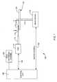
- FIG. 1there is shown a disk drive 100 in which the present invention may be embodied.
- a disk drive 100in which the present invention may be embodied.
- at least one rotatable magnetic disk 112is supported on a spindle 114 and rotated by a disk drive motor 118 .
- the magnetic recording on each diskis in the form of annular patterns of concentric data tracks (not shown) on the magnetic disk 112 .
- At least one slider 113is positioned near the magnetic disk 112 , each slider 113 supporting one or more magnetic head assemblies 121 . As the magnetic disk rotates, slider 113 moves radially in and out over the disk surface 122 so that the magnetic head assembly 121 may access different tracks of the magnetic disk where desired data are written.
- Each slider 113is attached to an actuator arm 119 by way of a suspension 115 .
- the suspension 115provides a slight spring force which biases slider 113 against the disk surface 122 .
- Each actuator arm 119is attached to an actuator means 127 .
- the actuator means 127 as shown in FIG. 1may be a voice coil motor (VCM).
- the VCMcomprises a coil movable within a fixed magnetic field, the direction and speed of the coil movements being controlled by the motor current signals supplied by controller 129 .
- the rotation of the magnetic disk 112generates an air bearing between the slider 113 and the disk surface 122 which exerts an upward force or lift on the slider.
- the air bearingthus counter-balances the slight spring force of suspension 115 and supports slider 113 off and slightly above the disk surface by a small, substantially constant spacing during normal operation.
- control unit 129The various components of the disk storage system are controlled in operation by control signals generated by control unit 129 , such as access control signals and internal clock signals.
- control unit 129comprises logic control circuits, storage means and a microprocessor.
- the control unit 129generates control signals to control various system operations such as drive motor control signals on line 123 and head position and seek control signals on line 128 .
- the control signals on line 128provide the desired current profiles to optimally move and position slider 113 to the desired data track on disk 112 .
- Write and read signalsare communicated to and from write and read heads 121 by way of recording channel 125 .
- FIG. 2is an ABS view of the slider 113 , and as can be seen the magnetic head including an inductive write head and a read sensor, is located at a trailing edge of the slider.
- the magnetic head including an inductive write head and a read sensoris located at a trailing edge of the slider.
- FIG. 1The above description of a typical magnetic disk storage system, and the accompanying illustration of FIG. 1 are for representation purposes only. It should be apparent that disk storage systems may contain a large number of disks and actuators, and each actuator may support a number of sliders.
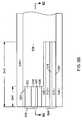
- a magnetoresistive sensor 300includes a magnetoresistive sensor element or sensor stack 302 , sandwiched between first and second electrically conductive lead layers 304 , 306 , which can be constructed of a magnetic material such as NiFe so that they serve as magnetic shields as well as electrical leads.
- the leads 304 , 306can be constructed of a non-magnetic material such as Au, Cu or some other electrically conductive material.
- An electrically insulating fill layer 305 , 307is provided at the sides of the sensor stack 302 .
- the fill layers 305 , 307can also be constructed of a magnetic material such as NiFe, however, if an electrically conductive material is used for the fill layer 305 , then a layer of insulation layer will be needed, both at the sides of the sensor stack 302 and across the surface of at least one of the leads 304 , 306 to prevent current from shunting through the fill layer 305 .
- the sensor stack 302includes a magnetic free layer 312 , a pinned layer structure 314 and a non-magnetic, electrically conductive spacer layer 316 , constructed of, for example Cu, sandwiched between the free layer 312 and the pinned layer 314 .
- the inventioncould also be embodied in a tunnel valve sensor in which case the layer 302 would be a thin, non-magnetic, electrically insulating barrier layer.
- the free layer 312can be constructed of several magnetic materials such as Co or CoFe, or of a combination of layers of different magnetic materials.
- the pinned layer structure 314 used in the embodiment described in FIG. 3Ais an AP pinned, self pinned structure.
- the pinned layer structure 314includes a first magnetic layer AP 1 318 , a second magnetic layer AP 2 320 , and an AP coupling layer 322 sandwiched between the AP1 and AP2 layers.
- the coupling layer 322can be for example Ru and is of such a thickness to strongly antiparallel couple the magnetic moments 319 , 321 of the AP1 and AP2 layers 318 , 320 .
- AP1 and AP2 layersare constructed of a material having a positive magnetostriction, such as for example CoFe.
- This positive magnetostrictionwhen combined with the compressive stresses that are inevitably present in thin film magnetoresistive sensors, causes a strong magnetic anisotropy in a direction perpendicular to the ABS.
- This magnetic anisotropywhen combined with the antiparallel (AP) coupling of the AP1 and AP2 layers 318 , 320 assists in the pinning of the magnetic moments 319 , 321 of the AP1 and AP2 layers 318 , 320 .
- the pinning strength of the self pinned structure 314is also greatly enhanced by a shape enhanced anisotropy that will be described further below with reference to FIG. 4 .
- As a self pinned sensor 314pinning can be maintained without the need for an AFM layer. The removal of the AFM layer results in large reduction in gap thickness, since AFM layers such as PtMn and IrMn must be very thick in order to function effectively as AFM layers.
- the sensor stack 302also may include a seed layer 326 formed at the bottom of the sensor stack 302 , which can be used to initiate a desired crystalline growth in the layers of the sensor stack 302 .
- a capping layer 328such as for example Ta or some other suitable material may be provided at the top of the sensor stack 302 to protect the layers of the sensor stack from damage during manufacturing processes such as annealing.
- the sensor stack 302has first and second lateral sides 330 , 332 that define the track width (TW) of the sensor.
- the free layer 312has a magnetic moment 330 that is biased in a desired direction parallel with the ABS.
- the in stack bias structurecan be of several designs, and preferably includes a magnetic bias layer 336 , that is separated from the free layer by a non-magnetic spacer layer 338 .
- the bias layer 336may be exchange coupled with a layer of antiferromagnetic material (AFM layer) 340 .
- the bias 336 layeris constructed of a magnetic material such as Co, CoFe, NiFe, etc.
- the spacer layer 338may be for example Ru and is of such a thickness to magnetostatically couple the bias layer 336 with the free layer 312 .
- the AFM layer 340can be constructed of, for example PtMn, IrMn or some other antiferromagnetic material, and is of such a thickness to exchange couple with the bias layer 336 and, thereby, strongly pin the moment 342 of the bias layer 336 .
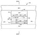
- the free layer 312 , and the in stack bias structureextend from the ABS a first stripe height distance SH 1 , whereas the pinned layer 314 and possibly a portion of the spacer layer 316 extend much further from the ABS to a second stripe height distance SH 2 .
- SH 2is preferably at least twice SH 1 and may be several times SH 1 (such as at least two times SH 1 ).
- SH 2is at least larger than SH 1 .
- ABSor air bearing surface refers to the surface of the sensor 300 that faces the magnetic medium during use. As fly heights become ever smaller, there may soon come a point where it will be difficult to distinguish whether the head is flying or in contact with the medium. Therefore, ABS should be understood to refer to the medium facing surface of the head, regardless of the fly height.
- the pinned layer 314being extended in the stripe height direction as described, has a strong shape enhanced magnetic anisotropy.
- This shape enhanced anisotropycan be several hundred Oe, greatly enhancing the pinning strength.
- This shape enhanced pinningallows the pinned layer 314 to be constructed as a self pinned sensor (pinned without the use of an AFM layer. Eliminating the AFM pinning layer, allows an optimal AFM material 340 to be used in the in stack bias structure 334 , without concern for setting (annealing) two different AFM layers.
- pinning of the pinned layer 314is also maintained by the positive magnetostriction of the AP1 and AP2 layers 318 , 320 , and by the AP coupling of the layers 318 , 320 , as discussed above.
- the inventioncould be embodied in a sensor 300 having an AFM pinned structure.
- a sensor 300would include a pinned layer 314 with an AP1 layer 318 that is exchange coupled with a layer of antiferromagnetic material (AFM layer) 324 .
- AFM layerantiferromagnetic material
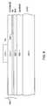
- the sensor 500has a partial mill design.
- the sensor 500includes a sensor stack 502 , having a pinned layer structure 504 , a free layer 506 and a non-magnetic, electrically conductive spacer layer 508 , constructed of, for example Cu.
- the inventioncould also be embodied in a tunnel valve sensor in which case the layer 508 would be a thin, non-magnetic, electrically insulating barrier layer.
- the free layer 506can be constructed of a magnetic material such as Co, CoFe, CoFeB, NiFe or a combination of these materials.
- the pinned layer 504is preferably an antiparallel coupled (AP coupled) structure including a first magnetic layer (AP 1 ) 510 , a second magnetic layer (AP 2 ) 512 and an AP coupling layer 514 sandwiched between the AP1 and AP2 layers.
- the AP1 and AP2 layers 510 , 512can be constructed of a magnetic material having a positive magnetostriction to assist pinning, such as for example CoFe.
- the AP coupling layer 514can be constructed of Ru.
- the sensor stack 502also includes an in stack bias structure 516 .
- the in stack bias structureincludes a magnetic biasing layer 518 , a non-magnetic spacer layer 520 and a layer of antiferromagnetic material (AFM layer) 522 .
- the magnetic bias layer 518can be constructed of, for example, Co, CoFe, NiFe, etc.
- the spacer layer 520can be constructed of, for example Ru, Cu or some other electrically conductive, non-magnetic material.
- the AFM layer 522can be, for example, PtMn or IrMn.
- the sensor stack 502may have a cap layer 524 , such as Ta to protect the sensor layers from damage during manufacture.
- a seed layer 526may also be provided at the bottom of the sensor stack 502 to promote a desired epitaxial growth in the sensor layers.
- first and second leads 528 , 530are sandwiched between first and second leads 528 , 530 .
- These leads 528 , 530are preferably constructed of a magnetic material such as NiFe so that they can function as magnetic shields as well as leads.
- first and second side shields 532 , 534may be provided at the sides of the sensor stack 502 .
- These side shields 532 , 534are constructed of a magnetic material such a NiFe.
- a thin electrical insulation layer 536such as conformally deposited alumina, is provided at either side of the sensor stack 502 and also extends across the surface of the extended portion of the sensor stack 502 . This insulation layer 536 prevents sense current from being shunted through the electrically conductive side shields 532 , 534 .
- the side shields 532 , 534could be eliminated, and could be replaced with an electrically insulating fill layer (not shown).
- the free layerextends to a first width to define a track width TW.
- the other layerswhich may include the spacer layer 508 and all or a portion of the pinned layer 504 , extend beyond the track width TW. Therefore, the trackwidth of the sensor 500 is defined by the width of the free layer 506 .
- the laterally extending portion of the pinned layer 504extends at least beyond the width of the free layer.
- the laterally extending portion of the free layerpreferably extends to a width at least twice the width of the free layer, and more preferably extends indefinitely in the lateral direction.
- this redeposited materialreduces the efficiency of the hard bias layers by increasing the distance between the hard bias layers and the free layer.
- this redepeposited materialis much more problematic, because it shunts sense current, dramatically decreasing the performance of the sensor.
- the free layer 506 , in stack bias structure 516 and possibly a portion of the spacer layer 508terminate at a first stripe height distance SH 1 as measured from the ABS.
- the pinned layer structureextends significantly beyond the first stripe height SH 1 to a second stripe height SH 2 , also measured from the ABS.
- the second stripe height distance SH 2is at least larger than the first stripe height distance SH 1 , and is preferably at least twice the first stripe height distance SH 1 . More preferably, the second stripe height distance is several times or three or more times the first stripe height distance.
- An electrically insulating, non-magnetic fill material 538such as alumina, fills the space behind the free layer 506 and in stack bias structure 516 .
- the laterally extended portion of the pinned layer structure 504has a stripe height that terminates at the stripe height SH 1 , at the same stripe height as that of the free layer 506 and in stack bias structure 516 (shown in FIG. 5B ).
- This stripe height SH 1 of the pinned layer structure 504is formed by a method that will be described herein below. Terminating the laterally extending portions of the pinned layer 504 at SH 1 as shown improves the shape enhanced anisotropy of the pinned layer 504 and improves magnetic performance of the sensor 500 .
- Extending the pinned layer 504 beyond the stripe height SH 1 of the sensor stack 502 to SH 2provides a very strong magnetic anisotropy in a direction perpendicular to the ABS.
- This shaped induced anisotropyis as high as several hundred Oe, assuring extremely strong pinning.
- this strong magnetic anisotropyis advantageously unaffected by other factors such as the size of the sensor or by mechanical stresses. What's more, this anisotropy is completely additive to other pinning mechanisms such as AP pinning, AFM pinning or pinning with a hard magnet.
- This methodmakes use of a single mask structure for multiple manufacturing processes, re-using a single mask structure so that multiple mask alignments are not necessary. It should be pointed out that while this recycled mask process is being described in terms of manufacturing the above described sensor structure, in a more general sense this multiple-use mask process can be used to construct many different structures including those other than read/write magnetic heads such as in semiconductor or integrated circuit designs. Furthermore, while the multiple-use mask process is described as using a single mask for two manufacturing processes the mask structure could be used more than two times for many multiple processes.
- a substratesuch as a first lead 602 is provided, on top of which the various sensor layers 604 are deposited as full film layers.
- the layer 604actually includes the various, multiple layers that make up the sensor stack 502 as described above, including the in stack bias structure 510 ( FIG. 5 ).
- a track width defining mask structure 605is then deposited by first depositing a layer of material that is resistant to chemical mechanical polishing (CMP resistant layer) 606 .
- This materialcan be, for example diamond like carbon (DLC). Although other materials could be used, this CMP resistant layer 606 will be referred to as DLC layer 606 .
- a layer of material 608 that is both resistant to removal by CMP and also resistant to removal by reactive ion etching (CMP resistant and RIE resistant)is then deposited full film over the DLC layer 608 .
- CMP resistant and RIE resistant layer 608the layer 608 is preferably constructed of Rh, and will hereinafter be referred to as Rh layer 608 . It should however be understood, that the layer 608 could be some material other than Rh.
- a transfer mask layer 610such as DURIMIDE® is then deposited and a photosensitive mask such as TIS or photoresist 612 is then constructed to have a width to define the track width of the sensor.
- the photoresist mask 612can be constructed according to methods that will be familiar to those skilled in the art, including spinning on a photoresist material and then patterning and developing the photoresist mask 612 .
- a 1 st reactive ion etch, (1 st RIE 702 )is performed to transfer the image of the photoresist layer 612 onto the underlying non-photosensitive material 610 .
- a first ion mill 802is performed to remove portions of the Rh layer that are not protect by the overlying mask layers 610 , 612 .
- a second RIE 902is performed to remove portions of the DLC layer that are not protected by the overlying mask layers 608 , 610 , 612 .
- FIG. 10shows the individual sensor layers so that this partial mill can be more clearly understood.
- a second ion mill 1002is performed, using mask layers 606 - 612 to define the track width of the sensor 300 ( FIG. 3 ) by removing portions of the sensor material 604 that are not protected by the overlying mask layers 606 - 612 .
- Thisis the first use of the mask structure 606 - 612 , in which the mask is used to define the trackwidth of the sensor.
- the ion mill 1002is performed sufficiently to remove the in stack bias structure 516 and the free layer 506 , but is preferably terminated before the pinned layer 504 has been removed.
- the ion mill 1002may be terminated when the spacer/barrier layer 508 has been reached. This is a partial mill process, wherein the track width is defined by the free layer, and the pinned layer and underlying AFM (if one is present) are left intact.
- FIG. 11which shows a top down view of the structure described in FIG. 10 , shows that the pattern defined in the sensor and mask layers 602 - 612 extends a substantial amount in the stripe height direction.
- a thin layer of non-magnetic, electrically insulating material 1202is deposited, preferably by a conformal deposition process such as atomic layer deposition, chemical vapor deposition, etc.
- the insulation layer 1202can be, for example alumina (Al 2 O 3 ) or some other material.
- a layer of magnetic material 1204(for magnetic shielding) is then deposited over the insulation layer 1202 .
- the shield material 1204can be for example NiFe or some other suitable material.
- a second layer of CMP resistant material (2 nd DLC layer) 1206is then deposited over the insulation and shield layers 1202 , 1204 .
- the shielding material 1204can be eliminated and insulation layer 1202 can be deposited to the level of the top of sensor layers 604 .
- a chemical mechanical polishing process(CMP) is performed.
- the CMPremoves the tall topography of the mask structure, planarizing the deposited structure down to the level of the Rh layer 608 and the second DLC layer 1206 .
- the Rh layer 608acts as a CMP stop layer that protects the sensor layers 604 from the CMP process, and the second DLC layer 1206 protects the insulation layer 1202 and magnetic shielding material 1204 .
- a second mask structure 1401is formed.
- the mask structurepreferably includes patterned TIS layer 1402 such as photoresist and an image transfer layer 1404 such as DURAMIDE.
- a third CMP resistant layer (3 rd DLC layer) 1406may also be deposited as a full film layer, beneath the image transfer layer 1404 and TIS 1402 .
- This second mask structure 1401is constructed to define the stripe height of the active area of the sensor by defining the stripe height of the free layer. In other words it covers the area from the ABS (future ABS location) to SH 1 . This can be seen more clearly with reference to FIG. 15 .
- a third reactive ion etch (RIE) 1702is performed.
- This third RIE 1702removes the second and third DLC layers 1206 , 1406 from the area over the magnetic shielding material 1204 .
- This third RIE 1702does not, however, remove the Rh layer 608 , because Rh layer 608 is resistant to removal by RIE.
- use of Rh for the RIE/CMP resistant layer 608is by way of example, and other materials could be used.
- a third ion mill 1802is performed.
- This ion mill 1802removes magnetic shield and insulation material 1202 , 1204 from the areas not covered by either of the first and second mask structures ( 605 , 1401 ) ( FIG. 17 ).
- This ion mill 1802also removes the remaining sensor material 604 (ie. the pinned layers 504 and any remaining spacer material 508 ) from the areas not covered by either of the first and second mask structures. Therefore, shield and insulation layers 1202 , 1204 and pinned layer 504 are removed only from areas beyond SH 1 (ie beyond the stripe height of the free layer as will be described below) and also outside of the trackwidth (TW).
- the third ion mill 1802also removes most or all of the Rh layer 608 , leaving the first DLC layer 606 exposed.
- the second mask structure 1402 , 1404is still in place so the insulation and shield layers 1202 , 1204 are unaffected by the third ion mill 1802 in areas adjacent to the active area of the sensor (between the ABS and SH 1 ).
- FIG. 19shows an isometric view of the structure thus far, which may better illustrate the structure.
- a fourth RIE 2002is performed to remove the first CMP layer 606 from over the sensor layers 604 in the area beyond SH 1 .
- the CMP layer 606can be readily removed by RIE 2002 .
- a fourth ion mill process 2102can be performed to remove selected portions of the sensor layer 604 .
- the ion mill process 2102can be performed sufficiently to remove the free layer 312 ( FIG. 3, 4 ) but can be terminated before removing the pinned layer structure 314 .
- the fourth ion mill process 2102can be performed sufficiently to leave all or a portion of the spacer 316 intact in the area beyond SH 1 .
- An insulation fill layer( 538 FIG. 5B, 5C ), can then be deposited to fill the areas removed during the third and fourth ion mills 1802 , 2102 .
- a masking and ion milling processmay also be performed to defined the further back stripe height (SH 2 ) of the extended pinned layer 504 .
- SH 2further back stripe height
- This SH 2 defining mask and milling processcan also be performed either before or after the processes described above, with reference to FIGS. 6-21 .
Landscapes
- Engineering & Computer Science (AREA)
- Manufacturing & Machinery (AREA)
- Physics & Mathematics (AREA)
- Chemical & Material Sciences (AREA)
- Nanotechnology (AREA)
- Condensed Matter Physics & Semiconductors (AREA)
- General Physics & Mathematics (AREA)
- Crystallography & Structural Chemistry (AREA)
- Hall/Mr Elements (AREA)
- Measuring Magnetic Variables (AREA)
- Magnetic Heads (AREA)
Abstract
Description
- The present invention relates to magnetoresistive sensors and more particularly the construction of a current perpendicular to plane magnetoresistive sensor having an in stack bias structure and a pinned layer that is extended in the stripe height direction to increase shape induced magnetic anisotropy and thereby improve pinning.
- The heart of a computer's long term memory is an assembly that is referred to as a magnetic disk drive. The magnetic disk drive includes a rotating magnetic disk, write and read heads that are suspended by a suspension arm adjacent to a surface of the rotating magnetic disk and an actuator that swings the suspension arm to place the read and write heads over selected circular tracks on the rotating disk. The read and write heads are directly located on a slider that has an air bearing surface (ABS). The suspension arm biases the slider into contact with the surface of the disk when the disk is not rotating but, when the disk rotates, air is swirled by the rotating disk. When the slider rides on the air bearing, the write and read heads are employed for writing magnetic impressions to and reading magnetic impressions from the rotating disk. The read and write heads are connected to processing circuitry that operates according to a computer program to implement the writing and reading functions.
- The write head includes a coil layer embedded in first, second and third insulation layers (insulation stack), the insulation stack being sandwiched between first and second pole piece layers. A gap is formed between the first and second pole piece layers by a gap layer at an air bearing surface (ABS) of the write head and the pole piece layers are connected at a back gap. Current conducted to the coil layer induces a magnetic flux in the pole pieces which causes a magnetic field to fringe out at a write gap at the ABS for the purpose of writing the aforementioned magnetic impressions in tracks on the moving media, such as in circular tracks on the aforementioned rotating disk.
- In recent read head designs a spin valve sensor, also referred to as a giant magnetoresistive (GMR) sensor, has been employed for sensing magnetic fields from the rotating magnetic disk. The sensor includes a nonmagnetic conductive layer, hereinafter referred to as a spacer layer, sandwiched between first and second ferromagnetic layers, hereinafter referred to as a pinned layer and a free layer. First and second leads are connected to the spin valve sensor for conducting a sense current therethrough. The magnetization of the pinned layer is pinned perpendicular to the air bearing surface (ABS) and the magnetic moment of the free layer is located parallel to the ABS, but free to rotate in response to external magnetic fields. The magnetization of the pinned layer is typically pinned by exchange coupling with an antiferromagnetic layer.
- The thickness of the spacer layer is chosen to be less than the mean free path of conduction electrons through the sensor. With this arrangement, a portion of the conduction electrons is scattered by the interfaces of the spacer layer with each of the pinned and free layers. When the magnetizations of the pinned and free layers are parallel with respect to one another, scattering is minimal and when the magnetizations of the pinned and free layer are antiparallel, scattering is maximized. Changes in scattering alter the resistance of the spin valve sensor in proportion to cos Θ, where Θ is the angle between the magnetizations of the pinned and free layers. In a read mode the resistance of the spin valve sensor changes proportionally to the magnitudes of the magnetic fields from the rotating disk. When a sense current is conducted through the spin valve sensor, resistance changes cause potential changes that are detected and processed as playback signals.
- When a spin valve sensor employs a single pinned layer it is referred to as a simple spin valve. When a spin valve employs an antiparallel (AP) pinned layer it is referred to as an AP pinned spin valve. An AP pinned spin valve includes first and second magnetic layers separated by a thin non-magnetic coupling layer such as Ru. The thickness of the spacer layer is chosen so as to antiparallel couple the magnetizations of the ferromagnetic layers of the pinned layer. A spin valve is also known as a top or bottom spin valve depending upon whether the pinning layer is at the top (formed after the free layer) or at the bottom (before the free layer).
- The spin valve sensor is located between first and second nonmagnetic electrically insulating read gap layers and the first and second read gap layers are located between ferromagnetic first and second shield layers. In a merged magnetic head a single ferromagnetic layer functions as the second shield layer of the read head and as the first pole piece layer of the write head. In a piggyback head the second shield layer and the first pole piece layer are separate layers.
- Magnetization of the pinned layer is usually fixed by exchange coupling one of the ferromagnetic layers (AP1) with a layer of antiferromagnetic material such as PtMn. While an antiferromagnetic (AFM) material such as PtMn does not in and of itself have a magnetization, when exchange coupled with a magnetic material, it can strongly pin the magnetization of the ferromagnetic layer.
- The push for ever increased data rate and data capacity has lead a drive to make magnetoresitive sensors ever smaller. For example, designing a sensor with a narrower track width means that more tracks of data can be fit onto a given area of magnetic medium. The various dimensions of a sensor must scale together, so if the trackwidth is decreased, then the stripe height dimension (perpendicular to the ABS) must also be decreased. As sensors become ever smaller, one problem that arises is that the pinned layer becomes impracticably unstable. In fact, future generation sensor will very soon become so small that the pinned layer will not be capable of being pinned by current pinning mechanisms. This has to do with the size of the pinned layer, which makes the pinned layer itself hard to pin, as well as the reduced area on which traditional pinning mechanisms such as AFM pinning, AP coupling, and magnetostriction induced anisotropy can act.
- Therefore, pinning stability of the sensor is one of the key concerns for higher areal recording density. This is especially true for current perpendicular to plane sensors such as current perpendicular to plane giant magnetoresistive (CPP GMR) and magnetic tunnel junction (MTJ) structures where the sensor dimensions will be 50 nm or below. CPP GMR sensors and MTJ sensors are of special interest, due to their capacity for higher signal amplitude. As mentioned above pinning strength deteriorates as the sensor dimensions get smaller. Furthermore, thinner sensor structures such as self pinned sensors are becoming more important, because of the drive to decrease gap thickness to decrease bit length. Therefore, pinning improvement for pinned and self pinned sensors is essential.
- The present invention provides a current perpendicular to plane magnetoresistive sensor having both an in-stack bias structure and a shape enhance pinned layer. The sensor includes a free layer, a pinned layer and either an electrically conductive spacer layer or an electrically insulating barrier layer sandwiched between the free layer and the pinned layer. The sensor has a surface intended for facing a magnetic medium during use (air bearing surface (ABS)). The free layer extends from the ABS to a first stripe height. The pinned layer, however, extends significantly beyond the first stripe height to terminate at a second stripe height that is further from the ABS than the first stripe height. The in-stack bias structure is formed adjacent to the free layer, opposite the spacer/barrier layer.
- Extending the pinned layer in the stripe height direction advantageously results in a strong magnetic anisotropy in a direction perpendicular to the ABS. This anisotropy, which can be several hundred Oe, greatly enhances pinning.
- The in stack bias structure advantageously eliminates the need for hard bias layer at the sides of the sensor and results in improved, uniform free layer biasing.
- The sensor can include a pinned layer that is either self pinned or pinned by exchange coupling with a layer of antiferromagnetic material AFM layer. If a self pinned pinned layer is used, the shape enhanced anisotropy maintains strong pinning, even without the use of an AFM layer. If the sensor is AFM pinned, the anisotropy prevents the setting of the AFM of the in-stack bias structure from affecting the pinning of the pinned layer.
- The sensor can also be embodied in a full mill sensor or in a partial mill sensor design in which only the free layer and in-stack bias structure are removed during the track width defining ion mill.
- These and other features and advantages of the invention will be apparent upon reading of the following detailed description of preferred embodiments taken in conjunction with the Figures in which like reference numerals indicate like elements throughout.
- For a fuller understanding of the nature and advantages of this invention, as well as the preferred mode of use, reference should be made to the following detailed description read in conjunction with the accompanying drawings which are not to scale.
FIG. 1 is a schematic illustration of a disk drive system in which the invention might be embodied;FIG. 2 is an ABS view of a slider illustrating the location of a magnetic head thereon;FIG. 3A is an ABS view, taken fromcircle 3 ofFIG. 2 illustrating a sensor according to an embodiment of the invention;FIG. 3B is an ABS view, similar toFIG. 3A illustrating a sensor according to an alternate embodiment of the invention;FIG. 4 is a side cross sectional view, taken from line4-4 ofFIG. 3 ;FIG. 5A is an ABS view of a sensor according to an embodiment of the invention;FIG. 5B is a sectional view taken fromline 5B-5B ofFIG. 5A ;FIG. 5C is a sectional view taken fromline 5C-5C ofFIG. 5B ; andFIGS. 6-21 are views of a magnetoresitive sensor according to an embodiment of the invention, shown in various intermediate stages of manufacture to illustrate a method of manufacturing a device according to an embodiment of the present invention.- The following description is of the best embodiments presently contemplated for carrying out this invention. This description is made for the purpose of illustrating the general principles of this invention and is not meant to limit the inventive concepts claimed herein.
- Referring now to
FIG. 1 , there is shown adisk drive 100 in which the present invention may be embodied. As shown inFIG. 1 , at least one rotatablemagnetic disk 112 is supported on aspindle 114 and rotated by adisk drive motor 118. The magnetic recording on each disk is in the form of annular patterns of concentric data tracks (not shown) on themagnetic disk 112. - At least one
slider 113 is positioned near themagnetic disk 112, eachslider 113 supporting one or moremagnetic head assemblies 121. As the magnetic disk rotates,slider 113 moves radially in and out over thedisk surface 122 so that themagnetic head assembly 121 may access different tracks of the magnetic disk where desired data are written. Eachslider 113 is attached to anactuator arm 119 by way of asuspension 115. Thesuspension 115 provides a slight spring force whichbiases slider 113 against thedisk surface 122. Eachactuator arm 119 is attached to an actuator means127. The actuator means127 as shown inFIG. 1 may be a voice coil motor (VCM). The VCM comprises a coil movable within a fixed magnetic field, the direction and speed of the coil movements being controlled by the motor current signals supplied bycontroller 129. - During operation of the disk storage system, the rotation of the
magnetic disk 112 generates an air bearing between theslider 113 and thedisk surface 122 which exerts an upward force or lift on the slider. The air bearing thus counter-balances the slight spring force ofsuspension 115 and supportsslider 113 off and slightly above the disk surface by a small, substantially constant spacing during normal operation. - The various components of the disk storage system are controlled in operation by control signals generated by
control unit 129, such as access control signals and internal clock signals. Typically, thecontrol unit 129 comprises logic control circuits, storage means and a microprocessor. Thecontrol unit 129 generates control signals to control various system operations such as drive motor control signals online 123 and head position and seek control signals online 128. The control signals online 128 provide the desired current profiles to optimally move andposition slider 113 to the desired data track ondisk 112. Write and read signals are communicated to and from write and readheads 121 by way ofrecording channel 125. - With reference to
FIG. 2 , the orientation of themagnetic head 121 in aslider 113 can be seen in more detail.FIG. 2 is an ABS view of theslider 113, and as can be seen the magnetic head including an inductive write head and a read sensor, is located at a trailing edge of the slider. The above description of a typical magnetic disk storage system, and the accompanying illustration ofFIG. 1 are for representation purposes only. It should be apparent that disk storage systems may contain a large number of disks and actuators, and each actuator may support a number of sliders. - With reference now to
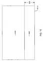
FIG. 3 , amagnetoresistive sensor 300 according to an embodiment of the invention includes a magnetoresistive sensor element orsensor stack 302, sandwiched between first and second electrically conductive lead layers304,306, which can be constructed of a magnetic material such as NiFe so that they serve as magnetic shields as well as electrical leads. Alternatively, theleads fill layer sensor stack 302. The fill layers305,307 can also be constructed of a magnetic material such as NiFe, however, if an electrically conductive material is used for thefill layer 305, then a layer of insulation layer will be needed, both at the sides of thesensor stack 302 and across the surface of at least one of theleads fill layer 305. - The
sensor stack 302 includes a magneticfree layer 312, a pinnedlayer structure 314 and a non-magnetic, electricallyconductive spacer layer 316, constructed of, for example Cu, sandwiched between thefree layer 312 and the pinnedlayer 314. The invention could also be embodied in a tunnel valve sensor in which case thelayer 302 would be a thin, non-magnetic, electrically insulating barrier layer. Thefree layer 312 can be constructed of several magnetic materials such as Co or CoFe, or of a combination of layers of different magnetic materials. - The pinned
layer structure 314 used in the embodiment described inFIG. 3A is an AP pinned, self pinned structure. The pinnedlayer structure 314 includes a firstmagnetic layer AP1 318, a secondmagnetic layer AP2 320, and anAP coupling layer 322 sandwiched between the AP1 and AP2 layers. Thecoupling layer 322 can be for example Ru and is of such a thickness to strongly antiparallel couple themagnetic moments AP2 layers AP2 layers magnetic moments AP2 layers structure 314 is also greatly enhanced by a shape enhanced anisotropy that will be described further below with reference toFIG. 4 . As a self pinnedsensor 314, pinning can be maintained without the need for an AFM layer. The removal of the AFM layer results in large reduction in gap thickness, since AFM layers such as PtMn and IrMn must be very thick in order to function effectively as AFM layers. - The
sensor stack 302 also may include aseed layer 326 formed at the bottom of thesensor stack 302, which can be used to initiate a desired crystalline growth in the layers of thesensor stack 302. Acapping layer 328, such as for example Ta or some other suitable material may be provided at the top of thesensor stack 302 to protect the layers of the sensor stack from damage during manufacturing processes such as annealing. Thesensor stack 302 has first and secondlateral sides free layer 312 has amagnetic moment 330 that is biased in a desired direction parallel with the ABS. - Biasing of the
moment 330 is achieved by a bias field provided by an instack bias structure 334. The in stack bias structure can be of several designs, and preferably includes amagnetic bias layer 336, that is separated from the free layer by anon-magnetic spacer layer 338. Thebias layer 336 may be exchange coupled with a layer of antiferromagnetic material (AFM layer)340. Thebias 336 layer is constructed of a magnetic material such as Co, CoFe, NiFe, etc. Thespacer layer 338 may be for example Ru and is of such a thickness to magnetostatically couple thebias layer 336 with thefree layer 312. TheAFM layer 340 can be constructed of, for example PtMn, IrMn or some other antiferromagnetic material, and is of such a thickness to exchange couple with thebias layer 336 and, thereby, strongly pin themoment 342 of thebias layer 336. - With reference to
FIG. 4 , it can be seen that thefree layer 312, and the in stack bias structure extend from the ABS a first stripe height distance SH1, whereas the pinnedlayer 314 and possibly a portion of thespacer layer 316 extend much further from the ABS to a second stripe height distance SH2. SH2 is preferably at least twice SH1 and may be several times SH1 (such as at least two times SH1). SH2 is at least larger than SH1. It should be pointed out that the term ABS (or air bearing surface) refers to the surface of thesensor 300 that faces the magnetic medium during use. As fly heights become ever smaller, there may soon come a point where it will be difficult to distinguish whether the head is flying or in contact with the medium. Therefore, ABS should be understood to refer to the medium facing surface of the head, regardless of the fly height. - The pinned
layer 314, being extended in the stripe height direction as described, has a strong shape enhanced magnetic anisotropy. This shape enhanced anisotropy can be several hundred Oe, greatly enhancing the pinning strength. This shape enhanced pinning allows the pinnedlayer 314 to be constructed as a self pinned sensor (pinned without the use of an AFM layer. Eliminating the AFM pinning layer, allows anoptimal AFM material 340 to be used in the instack bias structure 334, without concern for setting (annealing) two different AFM layers. In addition to the shape enhanced anisotropy, pinning of the pinnedlayer 314 is also maintained by the positive magnetostriction of the AP1 andAP2 layers layers - With reference to
FIG. 3B , the invention could be embodied in asensor 300 having an AFM pinned structure. Such asensor 300 would include a pinnedlayer 314 with anAP1 layer 318 that is exchange coupled with a layer of antiferromagnetic material (AFM layer)324. - With reference to
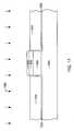
FIG. 5A , in an alternate embodiment of the invention, thesensor 500 has a partial mill design. Thesensor 500 includes asensor stack 502, having a pinnedlayer structure 504, afree layer 506 and a non-magnetic, electricallyconductive spacer layer 508, constructed of, for example Cu. The invention could also be embodied in a tunnel valve sensor in which case thelayer 508 would be a thin, non-magnetic, electrically insulating barrier layer. Thefree layer 506 can be constructed of a magnetic material such as Co, CoFe, CoFeB, NiFe or a combination of these materials. - The pinned
layer 504 is preferably an antiparallel coupled (AP coupled) structure including a first magnetic layer (AP1)510, a second magnetic layer (AP2)512 and anAP coupling layer 514 sandwiched between the AP1 and AP2 layers. The AP1 andAP2 layers AP coupling layer 514 can be constructed of Ru. - The
sensor stack 502 also includes an instack bias structure 516. The in stack bias structure includes amagnetic biasing layer 518, anon-magnetic spacer layer 520 and a layer of antiferromagnetic material (AFM layer)522. Themagnetic bias layer 518 can be constructed of, for example, Co, CoFe, NiFe, etc. Thespacer layer 520 can be constructed of, for example Ru, Cu or some other electrically conductive, non-magnetic material. TheAFM layer 522 can be, for example, PtMn or IrMn. In addition, thesensor stack 502 may have acap layer 524, such as Ta to protect the sensor layers from damage during manufacture. Aseed layer 526, may also be provided at the bottom of thesensor stack 502 to promote a desired epitaxial growth in the sensor layers. - The
sensor stack 502 is sandwiched between first andsecond leads sensor stack 502. These side shields532,534 are constructed of a magnetic material such a NiFe. A thinelectrical insulation layer 536, such as conformally deposited alumina, is provided at either side of thesensor stack 502 and also extends across the surface of the extended portion of thesensor stack 502. Thisinsulation layer 536 prevents sense current from being shunted through the electrically conductive side shields532,534. Alternatively, the side shields532,534 could be eliminated, and could be replaced with an electrically insulating fill layer (not shown). - With continued reference to
FIG. 5A , it can be seen that the free layer extends to a first width to define a track width TW. The other layers, which may include thespacer layer 508 and all or a portion of the pinnedlayer 504, extend beyond the track width TW. Therefore, the trackwidth of thesensor 500 is defined by the width of thefree layer 506. In this partial mill design, the laterally extending portion of the pinnedlayer 504 extends at least beyond the width of the free layer. The laterally extending portion of the free layer preferably extends to a width at least twice the width of the free layer, and more preferably extends indefinitely in the lateral direction. - To understand the advantages of this partial mill design it is necessary to understand the processes that are used to define the sensor stack. All of the sensor layers are first deposited full film, and then a mask having a width substantially equal to the track width TW is formed over the sensor layers. An ion mill is then used to remove sensor material not covered by the mask. Traditionally this ion mill has been performed sufficiently to remove all of the sensor material not covered by the mask down to the level of an underlying substrate such as the first lead (in the case of a CPP sensor) or first gap layer (in the case of a CIP) sensor.
- As the ion mill process removes sensor material, a certain amount of this material becomes redeposited on the sides of the sensor. In a CIP sensor this redeposited material (redep) reduces the efficiency of the hard bias layers by increasing the distance between the hard bias layers and the free layer. In a CPP sensor this redepeposited material is much more problematic, because it shunts sense current, dramatically decreasing the performance of the sensor.
- In the partial mill design described with reference to
FIGS. 5A-5C , only the instack bias layer 516 andfree layer 506 are removed during the track width defining ion mill process. Ion milling is stopped when the barrier orspacer layer 316 is reached. The pinnedlayer 314 remains after ion milling, as well as the underlying leads304. This greatly reduces the amount of redep because no pinned layer material or lead material is removed during the ion milling and cannot, therefore, be redeposited. A more detailed discussion of a method for constructing a sensor according to an embodiment of the invention will be provided below. - With reference now to
FIG. 5B , thefree layer 506, instack bias structure 516 and possibly a portion of thespacer layer 508 terminate at a first stripe height distance SH1 as measured from the ABS. The pinned layer structure extends significantly beyond the first stripe height SH1 to a second stripe height SH2, also measured from the ABS. The second stripe height distance SH2 is at least larger than the first stripe height distance SH1, and is preferably at least twice the first stripe height distance SH1. More preferably, the second stripe height distance is several times or three or more times the first stripe height distance. An electrically insulating,non-magnetic fill material 538, such as alumina, fills the space behind thefree layer 506 and instack bias structure 516. - With reference now to
FIG. 5C , it can be seen that the laterally extended portion of the pinnedlayer structure 504, has a stripe height that terminates at the stripe height SH1, at the same stripe height as that of thefree layer 506 and in stack bias structure516 (shown inFIG. 5B ). This stripe height SH1 of the pinnedlayer structure 504 is formed by a method that will be described herein below. Terminating the laterally extending portions of the pinnedlayer 504 at SH1 as shown improves the shape enhanced anisotropy of the pinnedlayer 504 and improves magnetic performance of thesensor 500. - Extending the pinned
layer 504 beyond the stripe height SH1 of thesensor stack 502 to SH2 provides a very strong magnetic anisotropy in a direction perpendicular to the ABS. This shaped induced anisotropy is as high as several hundred Oe, assuring extremely strong pinning. Furthermore, this strong magnetic anisotropy is advantageously unaffected by other factors such as the size of the sensor or by mechanical stresses. What's more, this anisotropy is completely additive to other pinning mechanisms such as AP pinning, AFM pinning or pinning with a hard magnet. - With reference now to
FIGS. 6-21 a novel manufacturing method is described. This method makes use of a single mask structure for multiple manufacturing processes, re-using a single mask structure so that multiple mask alignments are not necessary. It should be pointed out that while this recycled mask process is being described in terms of manufacturing the above described sensor structure, in a more general sense this multiple-use mask process can be used to construct many different structures including those other than read/write magnetic heads such as in semiconductor or integrated circuit designs. Furthermore, while the multiple-use mask process is described as using a single mask for two manufacturing processes the mask structure could be used more than two times for many multiple processes. - To illustrate the process with regard to the particular structure described above, with reference now to
FIG. 6 , a substrate, such as afirst lead 602 is provided, on top of which thevarious sensor layers 604 are deposited as full film layers. Although shown as a single layer inFIG. 6 , it will be understood that thelayer 604 actually includes the various, multiple layers that make up thesensor stack 502 as described above, including the in stack bias structure510 (FIG. 5 ). - With reference still to
FIG. 6 a track width definingmask structure 605 is then deposited by first depositing a layer of material that is resistant to chemical mechanical polishing (CMP resistant layer)606. This material can be, for example diamond like carbon (DLC). Although other materials could be used, this CMPresistant layer 606 will be referred to asDLC layer 606. - A layer of
material 608 that is both resistant to removal by CMP and also resistant to removal by reactive ion etching (CMP resistant and RIE resistant) is then deposited full film over theDLC layer 608. Although several materials could be used as such a CMP resistant and RIEresistant layer 608, thelayer 608 is preferably constructed of Rh, and will hereinafter be referred to asRh layer 608. It should however be understood, that thelayer 608 could be some material other than Rh. Atransfer mask layer 610 such as DURIMIDE® is then deposited and a photosensitive mask such as TIS orphotoresist 612 is then constructed to have a width to define the track width of the sensor. Thephotoresist mask 612 can be constructed according to methods that will be familiar to those skilled in the art, including spinning on a photoresist material and then patterning and developing thephotoresist mask 612. With reference now toFIG. 7 , a 1streactive ion etch, (1stRIE702) is performed to transfer the image of thephotoresist layer 612 onto the underlyingnon-photosensitive material 610. Then, with reference toFIG. 8 , afirst ion mill 802 is performed to remove portions of the Rh layer that are not protect by the overlying mask layers610,612. Thereafter, with reference toFIG. 9 a second RIE 902 is performed to remove portions of the DLC layer that are not protected by the overlying mask layers608,610,612. - Although the other figures showed the sensor layers604 as a single layer,
FIG. 10 shows the individual sensor layers so that this partial mill can be more clearly understood. With reference now toFIG. 10 a second ion mill 1002 is performed, using mask layers606-612 to define the track width of the sensor300 (FIG. 3 ) by removing portions of thesensor material 604 that are not protected by the overlying mask layers606-612. This is the first use of the mask structure606-612, in which the mask is used to define the trackwidth of the sensor. - The
ion mill 1002 is performed sufficiently to remove the instack bias structure 516 and thefree layer 506, but is preferably terminated before the pinnedlayer 504 has been removed. For example, theion mill 1002 may be terminated when the spacer/barrier layer 508 has been reached. This is a partial mill process, wherein the track width is defined by the free layer, and the pinned layer and underlying AFM (if one is present) are left intact. FIG. 11 , which shows a top down view of the structure described inFIG. 10 , shows that the pattern defined in the sensor and mask layers602-612 extends a substantial amount in the stripe height direction.- With reference now to
FIG. 12 , a thin layer of non-magnetic, electrically insulatingmaterial 1202 is deposited, preferably by a conformal deposition process such as atomic layer deposition, chemical vapor deposition, etc. Theinsulation layer 1202 can be, for example alumina (Al2O3) or some other material. A layer of magnetic material1204 (for magnetic shielding) is then deposited over theinsulation layer 1202. Theshield material 1204 can be for example NiFe or some other suitable material. A second layer of CMP resistant material (2ndDLC layer)1206 is then deposited over the insulation andshield layers material 1204 can be eliminated andinsulation layer 1202 can be deposited to the level of the top of sensor layers604. - With reference now to
FIG. 13 , a chemical mechanical polishing process (CMP) is performed. The CMP removes the tall topography of the mask structure, planarizing the deposited structure down to the level of theRh layer 608 and thesecond DLC layer 1206. TheRh layer 608 acts as a CMP stop layer that protects the sensor layers604 from the CMP process, and thesecond DLC layer 1206 protects theinsulation layer 1202 andmagnetic shielding material 1204. - With reference to
FIGS. 14 and 15 , asecond mask structure 1401 is formed. The mask structure preferably includes patternedTIS layer 1402 such as photoresist and animage transfer layer 1404 such as DURAMIDE. A third CMP resistant layer (3rdDLC layer)1406 may also be deposited as a full film layer, beneath theimage transfer layer 1404 andTIS 1402. Thissecond mask structure 1401 is constructed to define the stripe height of the active area of the sensor by defining the stripe height of the free layer. In other words it covers the area from the ABS (future ABS location) to SH1. This can be seen more clearly with reference toFIG. 15 . - With reference now to
FIGS. 16 and 17 , a third reactive ion etch (RIE)1702 is performed. This third RIE1702 removes the second andthird DLC layers magnetic shielding material 1204. This third RIE1702 does not, however, remove theRh layer 608, becauseRh layer 608 is resistant to removal by RIE. As mentioned before, use of Rh for the RIE/CMPresistant layer 608 is by way of example, and other materials could be used. - With reference now to
FIG. 18 , athird ion mill 1802 is performed. Thision mill 1802 removes magnetic shield andinsulation material FIG. 17 ). Thision mill 1802 also removes the remaining sensor material604 (ie. the pinnedlayers 504 and any remaining spacer material508) from the areas not covered by either of the first and second mask structures. Therefore, shield andinsulation layers layer 504 are removed only from areas beyond SH1 (ie beyond the stripe height of the free layer as will be described below) and also outside of the trackwidth (TW). Thethird ion mill 1802 also removes most or all of theRh layer 608, leaving thefirst DLC layer 606 exposed. With reference toFIG. 19 it can be seen that thesecond mask structure shield layers third ion mill 1802 in areas adjacent to the active area of the sensor (between the ABS and SH1).FIG. 19 shows an isometric view of the structure thus far, which may better illustrate the structure. - With reference now to
FIG. 20 a fourth RIE 2002 is performed to remove thefirst CMP layer 606 from over the sensor layers604 in the area beyond SH1. With thethird CMP layer 1406 removed during the third RIE1302 and theRh layer 608 removed during the previousion mill process 1802, theCMP layer 606 can be readily removed byRIE 2002. - With reference now to
FIG. 21 , a fourthion mill process 2102 can be performed to remove selected portions of thesensor layer 604. Theion mill process 2102 can be performed sufficiently to remove the free layer312 (FIG. 3, 4 ) but can be terminated before removing the pinnedlayer structure 314. The fourthion mill process 2102 can be performed sufficiently to leave all or a portion of thespacer 316 intact in the area beyond SH1. An insulation fill layer (538FIG. 5B, 5C ), can then be deposited to fill the areas removed during the third andfourth ion mills - A masking and ion milling process may also be performed to defined the further back stripe height (SH2) of the extended pinned
layer 504. As this masking and milling operation will be familiar to those skilled in the art, a more detailed description is not given here. This SH2 defining mask and milling process can also be performed either before or after the processes described above, with reference toFIGS. 6-21 . - While various embodiments have been described above, it should be understood that they have been presented by way of example only, and not limitation. Other embodiments falling within the scope of the invention may also become apparent to those skilled in the art. Thus, the breadth and scope of the invention should not be limited by any of the above-described exemplary embodiments, but should be defined only in accordance with the following claims and their equivalents.
Claims (35)
Priority Applications (2)
| Application Number | Priority Date | Filing Date | Title |
|---|---|---|---|
| US11/304,219US7522391B2 (en) | 2005-12-14 | 2005-12-14 | Current perpendicular to plane magnetoresistive sensor having a shape enhanced pinned layer and an in stack bias structure |
| CNB2006101667785ACN100502079C (en) | 2005-12-14 | 2006-12-14 | Current Perpendicular to Planar Magnetoresistive Sensors |
Applications Claiming Priority (1)
| Application Number | Priority Date | Filing Date | Title |
|---|---|---|---|
| US11/304,219US7522391B2 (en) | 2005-12-14 | 2005-12-14 | Current perpendicular to plane magnetoresistive sensor having a shape enhanced pinned layer and an in stack bias structure |
Publications (2)
| Publication Number | Publication Date |
|---|---|
| US20070133133A1true US20070133133A1 (en) | 2007-06-14 |
| US7522391B2 US7522391B2 (en) | 2009-04-21 |
Family
ID=38139029
Family Applications (1)
| Application Number | Title | Priority Date | Filing Date |
|---|---|---|---|
| US11/304,219Expired - Fee RelatedUS7522391B2 (en) | 2005-12-14 | 2005-12-14 | Current perpendicular to plane magnetoresistive sensor having a shape enhanced pinned layer and an in stack bias structure |
Country Status (2)
| Country | Link |
|---|---|
| US (1) | US7522391B2 (en) |
| CN (1) | CN100502079C (en) |
Cited By (10)
| Publication number | Priority date | Publication date | Assignee | Title |
|---|---|---|---|---|
| US20090321860A1 (en)* | 2008-06-30 | 2009-12-31 | Qimonda Ag | Integrated circuit having a magnetic tunnel junction device and method |
| US20110013317A1 (en)* | 2009-07-16 | 2011-01-20 | Western Digital (Fremont), Llc | Method and system for fabricating magnetic transducers with improved pinning |
| JP2011216890A (en)* | 2010-04-01 | 2011-10-27 | Seagate Technology Llc | Apparatus, method and magnetic sensor |
| US8227023B1 (en) | 2009-05-27 | 2012-07-24 | Western Digital (Fremont), Llc | Method and system for fabricating magnetic transducers with improved pinning |
| CN103383848A (en)* | 2012-04-30 | 2013-11-06 | 希捷科技有限公司 | Stack with wide seed layer |
| US8721903B2 (en)* | 2012-04-05 | 2014-05-13 | HGST Netherlands B.V. | Method for planarizing a perpendicular magnetic recording disk for thermally-assisted recording (TAR) |
| CN104050976A (en)* | 2013-03-12 | 2014-09-17 | 希捷科技有限公司 | Method and apparatus for chemical-mechanical polishing |
| JP2014220031A (en)* | 2013-05-06 | 2014-11-20 | シーゲイト テクノロジー エルエルシー | Data reader with back edge surface |
| US8941954B2 (en)* | 2012-12-19 | 2015-01-27 | HGST Netherlands B.V. | Magnetic sensor with extended pinned layer and partial wrap around shield |
| US11127422B1 (en) | 2020-07-01 | 2021-09-21 | Western Digital Technologies, Inc. | Magnetic read sensors and related methods having a rear hard bias and no AFM layer |
Families Citing this family (22)
| Publication number | Priority date | Publication date | Assignee | Title |
|---|---|---|---|---|
| CA2620886C (en)* | 2005-08-31 | 2017-03-14 | The Regents Of The University Of California | Cellular libraries of peptide sequences (clips) and methods of using the same |
| US7848061B2 (en)* | 2006-03-14 | 2010-12-07 | Hitachi Global Storage Technologies Netherlands B.V. | Current perpendicular to plane (CPP) magnetoresistive sensor with back flux guide |
| US9007727B2 (en)* | 2007-07-17 | 2015-04-14 | HGST Netherlands B.V. | Magnetic head having CPP sensor with improved stabilization of the magnetization of the pinned magnetic layer |
| JP5383145B2 (en)* | 2008-10-15 | 2014-01-08 | エイチジーエスティーネザーランドビーブイ | Magnetic read head |
| US8296930B2 (en) | 2009-12-22 | 2012-10-30 | Hitachi Global Storage Technologies Netherlands B.V. | Method for manufacturing a magnetoresistive sensor having a flat shield |
| US8089734B2 (en)* | 2010-05-17 | 2012-01-03 | Tdk Corporation | Magnetoresistive element having a pair of side shields |
| US8582249B2 (en)* | 2011-04-26 | 2013-11-12 | Seagate Technology Llc | Magnetic element with reduced shield-to-shield spacing |
| US8675318B1 (en) | 2011-11-22 | 2014-03-18 | Western Digital (Fremont), Llc | Method and system for providing a read transducer having a reduced shield-to-shield spacing |
| US9269382B1 (en) | 2012-06-29 | 2016-02-23 | Western Digital (Fremont), Llc | Method and system for providing a read transducer having improved pinning of the pinned layer at higher recording densities |
| US8711528B1 (en) | 2012-06-29 | 2014-04-29 | Western Digital (Fremont), Llc | Tunnel magnetoresistance read head with narrow shield-to-shield spacing |
| US8760822B1 (en) | 2012-11-28 | 2014-06-24 | Western Digital (Fremont), Llc | Method and system for providing a read transducer having an extended pinned layer and soft magnetic bias structures with improved stability |
| US8854773B2 (en)* | 2012-11-28 | 2014-10-07 | Seagate Technology Llc | Side shield biasing layer separated from an air bearing surface |
| US8842395B2 (en) | 2012-12-19 | 2014-09-23 | HGST Netherlands B.V. | Magnetic sensor having an extended pinned layer and shape enhanced bias structure |
| US9318130B1 (en) | 2013-07-02 | 2016-04-19 | Western Digital (Fremont), Llc | Method to fabricate tunneling magnetic recording heads with extended pinned layer |
| US9042062B2 (en) | 2013-08-27 | 2015-05-26 | HGST Netherlands B.V. | Magnetic sensor with recessed AFM shape enhanced pinning and soft magnetic bias |
| US9214172B2 (en) | 2013-10-23 | 2015-12-15 | Western Digital (Fremont), Llc | Method of manufacturing a magnetic read head |
| US9047893B1 (en)* | 2014-01-31 | 2015-06-02 | HGST Netherlands B.V. | Magnetic sensor having narrow trackwidth and small read gap |
| US9633679B2 (en) | 2014-05-06 | 2017-04-25 | Seagate Technology Llc | Sensor stack structure with RKKY coupling layer between free layer and capping layer |
| US9130055B1 (en) | 2014-05-07 | 2015-09-08 | HGST Netherlands B.V. | Magnetic recording head with CPP-GMR spin-valve sensor and extended pinned layer |
| US9147404B1 (en) | 2015-03-31 | 2015-09-29 | Western Digital (Fremont), Llc | Method and system for providing a read transducer having a dual free layer |
| CN105911103A (en)* | 2016-04-13 | 2016-08-31 | 南京工业大学 | Pinning spin valve structure, biomagnetic sensor and biomolecule detection method |
| US10311901B1 (en) | 2018-05-30 | 2019-06-04 | Western Digital Technologies, Inc. | Anisotropy field induced self pinned recessed antiferromagnetic reader |
Citations (19)
| Publication number | Priority date | Publication date | Assignee | Title |
|---|---|---|---|---|
| US5546253A (en)* | 1994-05-06 | 1996-08-13 | Quantum Corporation | Digitial output magnetoresistive (DOMR) head and methods associated therewith |
| US5576914A (en)* | 1994-11-14 | 1996-11-19 | Read-Rite Corporation | Compact read/write head having biased GMR element |
| US5668473A (en)* | 1992-12-21 | 1997-09-16 | Siemens, Aktiengesellschaft | Magnetoresistive sensor including shortened measuring layers |
| US6002553A (en)* | 1994-02-28 | 1999-12-14 | The United States Of America As Represented By The United States Department Of Energy | Giant magnetoresistive sensor |
| US6421212B1 (en)* | 1999-09-21 | 2002-07-16 | Read-Rite Corporation | Thin film read head structure with improved bias magnet-to-magnetoresistive element interface and method of fabrication |
| US6466419B1 (en)* | 2000-03-31 | 2002-10-15 | Seagate Technology Llc | Current perpendicular to plane spin valve head |
| US20030086216A1 (en)* | 2001-10-25 | 2003-05-08 | Tdk Corporation | Magneto-resistive device, and magnetic head and head suspension assembly using same |
| US20030179520A1 (en)* | 2002-03-20 | 2003-09-25 | Alps Electric Co., Ltd. | Magnetic sensing element provided with second antiferromagnetic layer on free magnetic layer side |
| US6671139B2 (en)* | 2002-01-31 | 2003-12-30 | International Business Machines Corporation | In-stack longitudinal bias structure for CIP spin valve sensors with bias layer electrically insulated from free layer |
| US20040114284A1 (en)* | 2002-09-25 | 2004-06-17 | Tdk Corporation | Thin-film magnetic head with current-perpendicular-to-the plane |
| US6757144B2 (en)* | 2002-01-18 | 2004-06-29 | International Business Machines Corporation | Flux guide read head with in stack biased current perpendicular to the planes (CPP) sensor |
| US6762915B2 (en)* | 2001-09-05 | 2004-07-13 | Seagate Technology Llc | Magnetoresistive sensor with oversized pinned layer |
| US20040207960A1 (en)* | 2003-04-18 | 2004-10-21 | Alps Electric Co., Ltd. | Self-pinned CPP giant magnetoresistive head with antiferromagnetic film absent from current path |
| US20040207962A1 (en)* | 2003-04-18 | 2004-10-21 | Alps Electric Co., Ltd. | CPP giant magnetoresistive head having antiferromagnetic film disposed in rear of element |
| US20040207959A1 (en)* | 2003-04-18 | 2004-10-21 | Alps Electric Co., Ltd. | CPP giant magnetoresistive head with large-area metal film provided between shield and element |
| US20050128652A1 (en)* | 2003-12-10 | 2005-06-16 | Freitag James M. | Self-pinned spin valve sensor having its first AP pinned layer thicker than its second AP pinned layer to reduce the likelihood of amplitude flip |
| US20050219772A1 (en)* | 1998-11-30 | 2005-10-06 | Nec Corporation | Magnetoresistive effect transducer having longitudinal bias layer directly connected to free layer |
| US7057859B2 (en)* | 2002-06-27 | 2006-06-06 | Tdk Corporation | Magneto-resistive device with reduced susceptibility to ion beam damage |
| US7310208B2 (en)* | 2004-06-21 | 2007-12-18 | Alps Electric Co., Ltd. | Magnetoresistive sensor containing self-pinned layer containing a plurality of magnetic sublayers with magnetostriction-enhancing layer made of a nonmagnetic material |
Family Cites Families (2)
| Publication number | Priority date | Publication date | Assignee | Title |
|---|---|---|---|---|
| JP2000187812A (en) | 1998-12-17 | 2000-07-04 | Read Rite Smi Kk | Thin-film magnetic head |
| JP2003077107A (en) | 2001-09-06 | 2003-03-14 | Sony Corp | Magneto-resistance effect type magnetic head |
- 2005
- 2005-12-14USUS11/304,219patent/US7522391B2/ennot_activeExpired - Fee Related
- 2006
- 2006-12-14CNCNB2006101667785Apatent/CN100502079C/ennot_activeExpired - Fee Related
Patent Citations (20)
| Publication number | Priority date | Publication date | Assignee | Title |
|---|---|---|---|---|
| US5668473A (en)* | 1992-12-21 | 1997-09-16 | Siemens, Aktiengesellschaft | Magnetoresistive sensor including shortened measuring layers |
| US6002553A (en)* | 1994-02-28 | 1999-12-14 | The United States Of America As Represented By The United States Department Of Energy | Giant magnetoresistive sensor |
| US5546253A (en)* | 1994-05-06 | 1996-08-13 | Quantum Corporation | Digitial output magnetoresistive (DOMR) head and methods associated therewith |
| US5576914A (en)* | 1994-11-14 | 1996-11-19 | Read-Rite Corporation | Compact read/write head having biased GMR element |
| US20050219772A1 (en)* | 1998-11-30 | 2005-10-06 | Nec Corporation | Magnetoresistive effect transducer having longitudinal bias layer directly connected to free layer |
| US6487056B1 (en)* | 1999-09-21 | 2002-11-26 | Read-Rite Corporation | Thin film read head structure with improved bias magnet-to-magnetoresistive element interface and method of fabrication |
| US6421212B1 (en)* | 1999-09-21 | 2002-07-16 | Read-Rite Corporation | Thin film read head structure with improved bias magnet-to-magnetoresistive element interface and method of fabrication |
| US6466419B1 (en)* | 2000-03-31 | 2002-10-15 | Seagate Technology Llc | Current perpendicular to plane spin valve head |
| US6762915B2 (en)* | 2001-09-05 | 2004-07-13 | Seagate Technology Llc | Magnetoresistive sensor with oversized pinned layer |
| US20030086216A1 (en)* | 2001-10-25 | 2003-05-08 | Tdk Corporation | Magneto-resistive device, and magnetic head and head suspension assembly using same |
| US6757144B2 (en)* | 2002-01-18 | 2004-06-29 | International Business Machines Corporation | Flux guide read head with in stack biased current perpendicular to the planes (CPP) sensor |
| US6671139B2 (en)* | 2002-01-31 | 2003-12-30 | International Business Machines Corporation | In-stack longitudinal bias structure for CIP spin valve sensors with bias layer electrically insulated from free layer |
| US20030179520A1 (en)* | 2002-03-20 | 2003-09-25 | Alps Electric Co., Ltd. | Magnetic sensing element provided with second antiferromagnetic layer on free magnetic layer side |
| US7057859B2 (en)* | 2002-06-27 | 2006-06-06 | Tdk Corporation | Magneto-resistive device with reduced susceptibility to ion beam damage |
| US20040114284A1 (en)* | 2002-09-25 | 2004-06-17 | Tdk Corporation | Thin-film magnetic head with current-perpendicular-to-the plane |
| US20040207959A1 (en)* | 2003-04-18 | 2004-10-21 | Alps Electric Co., Ltd. | CPP giant magnetoresistive head with large-area metal film provided between shield and element |
| US20040207962A1 (en)* | 2003-04-18 | 2004-10-21 | Alps Electric Co., Ltd. | CPP giant magnetoresistive head having antiferromagnetic film disposed in rear of element |
| US20040207960A1 (en)* | 2003-04-18 | 2004-10-21 | Alps Electric Co., Ltd. | Self-pinned CPP giant magnetoresistive head with antiferromagnetic film absent from current path |
| US20050128652A1 (en)* | 2003-12-10 | 2005-06-16 | Freitag James M. | Self-pinned spin valve sensor having its first AP pinned layer thicker than its second AP pinned layer to reduce the likelihood of amplitude flip |
| US7310208B2 (en)* | 2004-06-21 | 2007-12-18 | Alps Electric Co., Ltd. | Magnetoresistive sensor containing self-pinned layer containing a plurality of magnetic sublayers with magnetostriction-enhancing layer made of a nonmagnetic material |
Cited By (17)
| Publication number | Priority date | Publication date | Assignee | Title |
|---|---|---|---|---|
| US20090321860A1 (en)* | 2008-06-30 | 2009-12-31 | Qimonda Ag | Integrated circuit having a magnetic tunnel junction device and method |
| US7902616B2 (en)* | 2008-06-30 | 2011-03-08 | Qimonda Ag | Integrated circuit having a magnetic tunnel junction device and method |
| US8227023B1 (en) | 2009-05-27 | 2012-07-24 | Western Digital (Fremont), Llc | Method and system for fabricating magnetic transducers with improved pinning |
| US9007728B1 (en) | 2009-05-27 | 2015-04-14 | Western Digital (Fremont), Llc | Method and system for fabricating magnetic transducers with improved pinning |
| US20110013317A1 (en)* | 2009-07-16 | 2011-01-20 | Western Digital (Fremont), Llc | Method and system for fabricating magnetic transducers with improved pinning |
| US8164864B2 (en)* | 2009-07-16 | 2012-04-24 | Western Digital (Fremont), Llc | Method and system for fabricating magnetic transducers with improved pinning |
| JP2011216890A (en)* | 2010-04-01 | 2011-10-27 | Seagate Technology Llc | Apparatus, method and magnetic sensor |
| US8721903B2 (en)* | 2012-04-05 | 2014-05-13 | HGST Netherlands B.V. | Method for planarizing a perpendicular magnetic recording disk for thermally-assisted recording (TAR) |
| US8822046B2 (en)* | 2012-04-30 | 2014-09-02 | Seagate Technology Llc | Stack with wide seed layer |
| CN103383848A (en)* | 2012-04-30 | 2013-11-06 | 希捷科技有限公司 | Stack with wide seed layer |
| US9437224B2 (en) | 2012-04-30 | 2016-09-06 | Seagate Technology Llc | Stack with wide seed layer |
| US8941954B2 (en)* | 2012-12-19 | 2015-01-27 | HGST Netherlands B.V. | Magnetic sensor with extended pinned layer and partial wrap around shield |
| CN104050976A (en)* | 2013-03-12 | 2014-09-17 | 希捷科技有限公司 | Method and apparatus for chemical-mechanical polishing |
| JP2014220031A (en)* | 2013-05-06 | 2014-11-20 | シーゲイト テクノロジー エルエルシー | Data reader with back edge surface |
| EP2801976A3 (en)* | 2013-05-06 | 2015-03-11 | Seagate Technology LLC | Data reader with back edge surface |
| US11127422B1 (en) | 2020-07-01 | 2021-09-21 | Western Digital Technologies, Inc. | Magnetic read sensors and related methods having a rear hard bias and no AFM layer |
| US11430470B2 (en) | 2020-07-01 | 2022-08-30 | Western Digital Technologies, Inc. | Magnetic read sensors and related methods having a rear hard bias and no AFM layer |
Also Published As
| Publication number | Publication date |
|---|---|
| CN1983659A (en) | 2007-06-20 |
| CN100502079C (en) | 2009-06-17 |
| US7522391B2 (en) | 2009-04-21 |
Similar Documents
| Publication | Publication Date | Title |
|---|---|---|
| US7522391B2 (en) | Current perpendicular to plane magnetoresistive sensor having a shape enhanced pinned layer and an in stack bias structure | |
| US7580230B2 (en) | Magnetoresistive sensor having shape enhanced pinning, a flux guide structure and damage free virtual edges | |
| US7961440B2 (en) | Current perpendicular to plane magnetoresistive sensor with reduced read gap | |
| US7602589B2 (en) | Magnetoresistive sensor having shape enhanced pinning and low lead resistance | |
| US7639456B2 (en) | Double mill process for patterning current perpendicular to plane (CPP) magnetoresistive devices to minimize barrier shorting and barrier damage | |
| US9042062B2 (en) | Magnetic sensor with recessed AFM shape enhanced pinning and soft magnetic bias | |
| US7712206B2 (en) | Method for manufacturing a magnetic write head having a trailing shield with an accurately controlled trailing shield gap thickness | |
| US7405909B2 (en) | Current perpendicular to plane (CPP) magnetoresistive sensor with free layer biasing by exchange pinning at back edge | |
| US7369371B2 (en) | Magnetoresistive sensor having a shape enhanced pinned layer | |
| US7324310B2 (en) | Self-pinned dual CPP sensor exchange pinned at stripe back-end to avoid amplitude flipping | |
| US7420787B2 (en) | Magnetoresistive sensor having a shape enhanced pinned layer | |
| US8213132B2 (en) | Magnetic sensor having a physically hard insulation layer over a magnetic bias structure | |
| US7369374B2 (en) | Current in plane magnetoresistive sensor having a contiguous hard bias layer located at back edge of stripe height | |
| US9202482B2 (en) | Magnetic sensor having an extended pinned layer with stitched antiferromagnetic pinning layer | |
| US7663846B2 (en) | Magnetoresistive sensor having an enhanced lead overlay design and shape enhanced pinning | |
| US7467459B2 (en) | Method for manufacturing a current in plane magnetoresistive sensor having a contiguous hard bias layer located at back edge of stripe height | |
| US20070109692A1 (en) | Oblique angle etched underlayers for improved exchange biased structures in a magnetoresitive sensor | |
| US7848061B2 (en) | Current perpendicular to plane (CPP) magnetoresistive sensor with back flux guide | |
| US7333305B2 (en) | Magnetoresistive sensor with in-stack bias layer pinned at the back edge of the sensor stripe | |
| US7765676B2 (en) | Method for patterning a magnetoresistive sensor | |
| US7329362B2 (en) | Dual angle milling for current perpendicular to plane (CPP) magnetoresistive sensor definition | |
| US7676905B2 (en) | Method of manufacturing a self aligned magnetoresistive sensor | |
| US20090161269A1 (en) | Magnetoresistive sensor having an enhanced free layer stabilization mechanism | |
| US8223462B2 (en) | Magnetoresistive sensor design for signal noise pickup reduction for use with deep gap electrostatic discharge shunt | |
| US7324311B2 (en) | Rie defined CPP read heads |
Legal Events
| Date | Code | Title | Description |
|---|---|---|---|
| AS | Assignment | Owner name:HITACHI GLOBAL STORAGE TECHNOLOGIES NETHERLANDS B. Free format text:ASSIGNMENT OF ASSIGNORS INTEREST;ASSIGNORS:FREITAG, JAMES MAC;HO, KUOK SAN;PINARBASI, MUSTAFA MICHAEL;AND OTHERS;REEL/FRAME:017182/0249;SIGNING DATES FROM 20051201 TO 20051209 | |
| FEPP | Fee payment procedure | Free format text:PAYOR NUMBER ASSIGNED (ORIGINAL EVENT CODE: ASPN); ENTITY STATUS OF PATENT OWNER: LARGE ENTITY | |
| FPAY | Fee payment | Year of fee payment:4 | |
| AS | Assignment | Owner name:HGST, NETHERLANDS B.V., NETHERLANDS Free format text:CHANGE OF NAME;ASSIGNOR:HGST, NETHERLANDS B.V.;REEL/FRAME:029341/0777 Effective date:20120723 Owner name:HGST NETHERLANDS B.V., NETHERLANDS Free format text:CHANGE OF NAME;ASSIGNOR:HITACHI GLOBAL STORAGE TECHNOLOGIES NETHERLANDS B.V.;REEL/FRAME:029341/0777 Effective date:20120723 | |
| REMI | Maintenance fee reminder mailed | ||
| AS | Assignment | Owner name:WESTERN DIGITAL TECHNOLOGIES, INC., CALIFORNIA Free format text:ASSIGNMENT OF ASSIGNORS INTEREST;ASSIGNOR:HGST NETHERLANDS B.V.;REEL/FRAME:040819/0450 Effective date:20160831 | |
| LAPS | Lapse for failure to pay maintenance fees | ||
| STCH | Information on status: patent discontinuation | Free format text:PATENT EXPIRED DUE TO NONPAYMENT OF MAINTENANCE FEES UNDER 37 CFR 1.362 | |
| FP | Lapsed due to failure to pay maintenance fee | Effective date:20170421 |