US20070131961A1 - AlInGaP LED Having Reduced Temperature Dependence - Google Patents
AlInGaP LED Having Reduced Temperature DependenceDownload PDFInfo
- Publication number
- US20070131961A1 US20070131961A1US11/672,003US67200307AUS2007131961A1US 20070131961 A1US20070131961 A1US 20070131961A1US 67200307 AUS67200307 AUS 67200307AUS 2007131961 A1US2007131961 A1US 2007131961A1
- Authority
- US
- United States
- Prior art keywords
- layer
- lattice constant
- substrate
- growth
- epitaxial
- Prior art date
- Legal status (The legal status is an assumption and is not a legal conclusion. Google has not performed a legal analysis and makes no representation as to the accuracy of the status listed.)
- Granted
Links
Images


Classifications
- H—ELECTRICITY
- H10—SEMICONDUCTOR DEVICES; ELECTRIC SOLID-STATE DEVICES NOT OTHERWISE PROVIDED FOR
- H10H—INORGANIC LIGHT-EMITTING SEMICONDUCTOR DEVICES HAVING POTENTIAL BARRIERS
- H10H20/00—Individual inorganic light-emitting semiconductor devices having potential barriers, e.g. light-emitting diodes [LED]
- H10H20/80—Constructional details
- H10H20/81—Bodies
- H10H20/822—Materials of the light-emitting regions
- H10H20/824—Materials of the light-emitting regions comprising only Group III-V materials, e.g. GaP
- H—ELECTRICITY
- H01—ELECTRIC ELEMENTS
- H01L—SEMICONDUCTOR DEVICES NOT COVERED BY CLASS H10
- H01L2224/00—Indexing scheme for arrangements for connecting or disconnecting semiconductor or solid-state bodies and methods related thereto as covered by H01L24/00
- H01L2224/01—Means for bonding being attached to, or being formed on, the surface to be connected, e.g. chip-to-package, die-attach, "first-level" interconnects; Manufacturing methods related thereto
- H01L2224/10—Bump connectors; Manufacturing methods related thereto
- H01L2224/12—Structure, shape, material or disposition of the bump connectors prior to the connecting process
- H01L2224/13—Structure, shape, material or disposition of the bump connectors prior to the connecting process of an individual bump connector
- H—ELECTRICITY
- H01—ELECTRIC ELEMENTS
- H01L—SEMICONDUCTOR DEVICES NOT COVERED BY CLASS H10
- H01L2924/00—Indexing scheme for arrangements or methods for connecting or disconnecting semiconductor or solid-state bodies as covered by H01L24/00
- H01L2924/0001—Technical content checked by a classifier
- H01L2924/00011—Not relevant to the scope of the group, the symbol of which is combined with the symbol of this group
- H—ELECTRICITY
- H01—ELECTRIC ELEMENTS
- H01L—SEMICONDUCTOR DEVICES NOT COVERED BY CLASS H10
- H01L2924/00—Indexing scheme for arrangements or methods for connecting or disconnecting semiconductor or solid-state bodies as covered by H01L24/00
- H01L2924/0001—Technical content checked by a classifier
- H01L2924/00014—Technical content checked by a classifier the subject-matter covered by the group, the symbol of which is combined with the symbol of this group, being disclosed without further technical details
Definitions
- This inventionrelates to light emitting diodes (LEDs) and, in particular, to a technique for forming AlInGaP LEDs whose visible light output has a reduced temperature dependence.
- Al x Ga 1-x ) 1-y In y P LEDsare used to produce visible wavelengths from red to amber.
- AlInGaP LEDsare typically formed by growing epitaxial layers, including p-type and n-type layers sandwiching a light-emitting active layer, on a GaAs growth substrate. High quality ternary and quaternary substrates are very difficult to fabricate, so GaAs substrates are commonly used.
- the lattice constant of the (Al x Ga 1-x ) 1-y In y P epitaxial layersmust match the lattice constant of the GaAs.
- y0.48. The x value is adjusted to achieve the desired emission wavelength.
- the light output of AlInGaP LEDsis highly dependent on temperature. For example, at temperatures in the range of 80-120 degrees C., the internal quantum efficiency at useful wavelengths is significantly reduced, resulting in a light output of two-thirds to one-half of the light output at room temperature. This variation in light output is extremely significant in certain applications such as traffic lights, tail lights, and displays.
- AlInGaP LEDshave a reduced temperature sensitivity if the lattice constant of the AlInGaP active layer is greater than that of GaAs.
- the lattice constantmay be increased by increasing the percentage of indium. Increasing the lattice constant increases the percentage of direct band gap (vs. indirect band gap) recombination, thus increasing quantum efficiency.
- GaAs and Geare practical growth substrates for AlInGaP LEDs, each having a similar lattice constant, approximately 5.65 ⁇ .
- an engineered growth layeris formed over a substrate, where the growth layer has a lattice constant equal to or approximately equal to the desired AlInGaP epitaxial layers for the light emitting device.
- the growth layerhas a composition of (Al x Ga 1-x ) 1-y In y P, where 0 ⁇ x ⁇ 1.0, and y>0.48.
- a graded InGaAs or, InGaP layeris grown over a GaAs or Ge substrate.
- the amount of indiumis increased during growth of the layer such that the final lattice constant is equal to that for the desired bandgap properties in the AlInGaP active layers.
- the residual strainis relatively low, resulting in an acceptable dislocation density (e.g., ⁇ 10E6/cm 2 ).
- a thick ( ⁇ 5 to 100 um) transparent window layerfor example GaP, AlGaP, or AlGaAs, may be grown above the AlInGaP active LED layers. This layer provides increased light extraction and current spreading for the LED devices.
- the resulting wafermay be metallized and diced, and mounted into packages, to provide operating LEDs.
- a distributed-Bragg-reflector (DBR) epitaxial layer stackfor example AlGaAs/AlGaAs, may be grown between the absorbing buffer layers and the LED active region, to reflect downward light towards the top surface of the chip, to increase LED brightness.
- DBRdistributed-Bragg-reflector
- a very thin InGaP, InGaAs, or AlInGaP layeris grown on a GaAs or Ge growth substrate, where the InGaP, InGaAs, or AlInGaP layer is fully strained (compressed) and free of additional dislocations caused by the heteroepitaxy.
- Hydrogen ionsare implanted into the top surface of the growth substrate.
- the waferis then bonded to an oxide bonding layer grown on a carrier substrate, which may be Si, Ge, GaAs, or other semiconductor, ceramic or metal, or alloys thereof.
- the resulting structureis heated, forming hydrogen bubbles that delaminate the InGaP, InGaAs, or AlInGaP layer from the growth substrate.
- the InGaP, InGaAs, or AlInGaP layerthen relaxes so that its lattice constant increases.
- the oxide bonding layeris optional if the wafer bond allows the strained layer to expand.
- the indium contentis selected such that the released InGaP, InGaAs, or AlInGaP layer has the same lattice constant as the desired overlying AlInGaP epitaxial layers.
- the AlInGaP LED layersare then grown over the relaxed InGaP, InGaAs, or AlInGaP layer. Subsequently, the LED layers may be bonded to a final host substrate or package element, and the carrier substrate and oxide layer are removed, for example, by etching or lapping, or any combination thereof.
- Light extraction featuressuch as shapes or texturing (either random or ordered), or a photonic crystal structure, may be applied to the top surface of the LED structure. Electrical contacts are made to the LED layers, and the wafer is diced. The resulting chips are mounted into packages to provide operating LEDs.
- the same device fabrication methodcould be applied to the technique of using InGaP or InGaAs graded buffer layers, described above.
- a thick ( ⁇ 5 to 100 um) transparent window layerfor example GaP, AlGaP, or AlGaAs
- the carrier substrate and oxide layermay be removed, with mechanical support for the remaining structure provided by the thick window layer.
- the resulting structuremay be bonded to a conductive, transparent substrate, such as GaP using elevated temperature and pressure.
- the wafer bonding conditionsmay be chosen so that the bonded interface provides both good electrical conductivity as well as optical transparency.
- the resulting wafermay be metallized and diced, and mounted into packages, to provide fully transparent LEDs.
- the same device fabrication methodcould be applied to the technique of using InGaP or InGaAs graded buffer layers.
- an AlInGaP LED with base LED epitaxial layers having an enlarged lattice constantdesirably affects the properties of the AlInGaP active layer.
- the AlInGaP active layermay even have a composition such that it is stressed or strained, since its lattice constant is constrained to the enlarged lattice constant of the epitaxial growth layers.
- the active layermay be multiple layers including quantum wells.
- FIGS. 1A and 1Bare diagrams showing examples of a conduction band edge and valence band edge that provides a direct band gap for efficiently producing light.
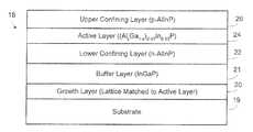
- FIG. 2is a cross-sectional view of an AlInGaP LED having an enlarged lattice constant formed by engineering a growth layer having a lattice constant greater than that of GaAs and equal to the lattice constant of the desired AlInGaP layers.
- FIG. 3is a diagram showing the reduced temperature dependence of a (Al x Ga 1-x ) 1-y In y P LED when y has been increased from 0.48 (matched to GaAs) to 0.53.
- FIG. 4is a diagram of lattice constant vs. energy gap for various substrates, including GaAs, illustrating the Applicants' desired increase in the lattice constant of AlInGaP LED layers from 5.65 angstroms (the lattice constant of GaAs) to between 5.65 and 5.73 ⁇ to reduce the temperature sensitivity of the AlInGaP LED.
- FIG. 5is a cross-sectional view of an AlInGaP LED having an enlarged lattice constant grown over a graded InGaAs or InGaP layer.
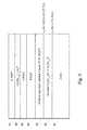
- FIGS. 6A-6Fare cross-sectional views of an LED structure at various stages of manufacture when forming an engineered growth layer, having a lattice constant larger than the lattice constant of GaAs, and growing AlInGaP epitaxial layers on the growth layer.
- FIGS. 7A-7Bare cross-sectional views of another LED structure at various stages of manufacture where a thick top window is formed (after the step of FIG. 6F ), and the light absorbing carrier substrate (e.g., silicon), along with other layers, are removed and optionally replaced with a transparent substrate.
- a thick top windowis formed (after the step of FIG. 6F )
- the light absorbing carrier substratee.g., silicon
- FIGS. 8A-8Bare cross-sectional views of another LED structure at various stages of manufacture where a reflector (e.g., metal mirror or Bragg reflector) and support substrate are bonded over the p-layers, and the light absorbing carrier substrate (e.g., silicon), along with other layers, are removed.
- a reflectore.g., metal mirror or Bragg reflector
- support substratee.g., silicon
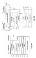
- FIGS. 9A-9Care cross-sectional views of another LED structure at various stages of manufacture where the device is formed as a flip chip, with the light absorbing carrier substrate (e.g., silicon) and other layers removed, and the top surface of the chip further processed (e.g., roughened) to for light extraction features.
- the light absorbing carrier substratee.g., silicon
- the top surface of the chipfurther processed (e.g., roughened) to for light extraction features.
- FIG. 10is an exploded view of one embodiment of a package for the resulting LED.
- FIG. 1Ais a simplified representation of energy vs. k-vector for a direct band gap semiconductor material, where the valence band maximum has the same k-vector as the conduction band minimum. In reality, the energy vs. k-vector curves are not as simple.
- FIG. 1Bis an energy vs. k-vector diagram for a direct band gap zinc blende semiconductor showing a direct band gap minimum (F) and indirect band gap minima (L and X) for the conduction band.
- Fdirect band gap minimum
- L and Xindirect band gap minima
- the F minimummust be at a lower energy than the L or X minima for an electron to efficiently cross the gap between the valence band and the conduction band to create a direct band gap transition and produce light. If the X or L minima were at an energy level lower than the F energy level, an increased carrier population would be involved in an indirect band gap transition and not produce light.
- reason #1 abovedominates the temperature sensitivity.
- xAl content
- Increasing xis necessary to shorten the emission wavelengths from 650 nm (deep red) to 560 nm (yellow/green).
- a higher Al contentis needed for efficient photometric operation at elevated temperatures, since thermal lattice expansion leads to a significant red-shift in emission peak wavelength ( ⁇ 0.1-0.2 nm/K).
- Applicantssought a way to increase the energy separation between the ⁇ and L minima in the active region to reduce the percentage of indirect band gap transitions with increasing temperature and thus reduce the temperature dependence of (Al x Ga 1-x ) 1-y In y P LEDs.
- an enlarged-lattice constant AlInGaP active layersubstantially reduces the temperature dependence of the LED by increasing the energy separation between the F and L minima.
- y in conventional LEDsis set to 0.48 in order for the material to match the lattice constant of the GaAs growth substrate so as to have relatively few dislocation defects. A higher value of y would result in the LED material grown on the GaAs substrate to have an unacceptably high density of dislocations.
- Other (Al x Ga 1-x ) 1-y In y P materials, where y>0.48,may also be engineered to have a desired large lattice constant to reduce the temperature dependence.
- FIG. 2is a cross-sectional view of one embodiment of an LED 18 where the active layer has a composition of (Al x Gal ) 0.47 In 0.53 P (lattice constant is larger than that of GaAs).
- a substrate 19has a growth layer 20 formed thereon.
- the growth layer 20has the same or approximately the same lattice constant as the overlying layers, including the active layer.
- An InGaP buffer layer 21is grown over the growth layer 20 .
- a lower confining layer 22 of n-type AlInPis grown on the buffer layer 21 .
- the AlInP confining layer 22has a band gap that is higher than the band gap of the active layer.
- a p-type upper confining layer 26 of AlInPis grown over the active layer 24 .
- a highly doped p-type AlInGaP contact layermay be provided over layer 26 .
- a p-metal electrode and an n-metal electrodeare formed in electrical contact with the p and n-type confining layers, respectively, for forward biasing the LED and injecting electrons and holes into the active layer 24 for radiative recombination.
- the Al content in the active layer 24is selected for the desired visible wavelength (e.g., red through green).
- the relatively large lattice constant of the AlInP confining layerscauses the band gap energy of the confining layers to slightly decrease (e.g., by 12 meV) as compared to AlInP with a lattice constant equal to that of GaAs. Although this reduces the effectiveness of the confining layers in confining the injected carriers to the active layer, the increased direct band gap recombination due to the larger lattice constant of the active layer more than offsets this drawback.
- FIG. 3is a graph showing the predicted reduced temperature dependence of the (Al x Ga 1-x ) 1-y In y P LED when y has been increased from 0.48 to 0.53. The external and internal quantum efficiencies are plotted vs. the p-n junction temperature.
- the composition of the AlInGaP active layerneed not be selected to precisely match that of the enlarged-lattice constant of the other AlInGaP epitaxial layers in the stack (e.g., y in the active layer need not equal y in the underlying layers).
- the composition of the AlInGaP active layermay be selected such that the active layer is stressed or strained, without having unacceptable defects, since its lattice constant is constrained to the enlarged lattice constant of the epitaxial growth layers beneath. That is, the active light emitting layers or other layers within the active region may be provided under tensile or compressive strain with respect to the underlying AlInGaP epitaxial layers.
- FIG. 4is a diagram of energy gap vs. lattice constant for constituent materials that make up the (Al x Ga 1-x ) 1-y In y P system.
- the lattice constant of the preferred AlInGaP materialis greater than 5.65 ⁇ and less than about 5.73 ⁇ . This corresponds to a region from y>0.48 to y ⁇ 0.66 if the AlInGaP active layer is not stressed or strained.
- FIG. 5illustrates one method to form an AlInGaP active layer with a lattice constant greater than that of GaAs.
- FIG. 5shows a cross-sectional view of a starting GaAs substrate 40 , having a lattice constant of 5.65 ⁇ .
- a graded In x Ga 1-x As buffer layer 42is grown on the GaAs substrate 40 until the lattice constant is the same as that desired for the AlInGaP LED layers.
- xis graded from 0 to 0.08 over a thickness of approximately 1 micron to achieve a lattice constant of 5.69 ⁇ .
- a maximum xis about 0.18.
- An x of 0.18will achieve a lattice constant of about 5.73 ⁇ .
- U.S. Pat. No. 6,232,138incorporated herein by reference, which describes engineering a growth layer for forming light emitting layers with new material systems, in particular AlInGaAs infrared lasers and transistors.
- the reason for engineering the growth layeris not for a new material system but for improved temperature sensitivity for a commonly used material system.
- the percentage of Inincreases to a point slightly below the top surface of the graded layer then is reduced by a small amount for the remainder of the thickness to achieve the intended lattice constant at the top surface.
- a uniform cap layer 43 of InGaAsmay be grown to reduce defect density.
- the uniform layer 43may have an In composition slightly less than that of the maximum In composition achieved within the graded buffer layer 42 .
- An InGaP buffer layer 44is then grown followed by an n-type AlInP confining layer 46 . If the graded buffer layer 42 is In y Ga 1-y P, the cap layer 43 may be the InGaP buffer layer 44 .
- a light-emitting AlInGaP LED active layer 48is then grown having the desired enlarged lattice constant, such as (Al x Ga 1-x ) 0.47 In 0.53 P for emitting visible red light or shorter wavelengths.
- the suitable indium content in the active layer for a particular growth layere.g., cap or graded layer
- the wavelengthis between 630 nm (red) and 560 nm (green).
- a p-type AlInP upper confining layer 50is then grown.
- a highly doped p-type (Al,In,Ga)P contact layermay then be provided over layer 50 .
- Other compositions of confining layersmay also be used.
- a thick ( ⁇ 5 to 100 um) transparent window layerfor example GaP, AlGaP, or AlGaAs, may be grown above the AlInGaP LED layers.
- This layerprovides increased light extraction and current spreading for the LED devices, and is not required to be latticed matched to the underlying layers.
- Suitable n and p metal contactsare then formed on the top and bottom surfaces.
- the waferis diced, and chips are mounted into packages to form operable LEDs.
- One method of forming an AlInGaP LEDis described in U.S. Pat. No. 6,525,335 to Krames et al., incorporated herein by reference.
- the lattice constant of the LED layersmay differ slightly from that of the uniform cap layer 43 without incurring unacceptable defects.
- the GaAs substrate 40 and graded InGaAs layer 42are to be used for conducting current to the n side of the pn junction, those materials would be n-doped.
- the light-absorbing GaAs and InGaAs materialsmay be removed and replaced by a transparent substrate bonded below the lower confining layer 46 .
- a fully transparent LED chipis possible.
- the p and n layersare electrically contacted by metal layers on the same side of the chip to form a flip chip, where the p and n-metal contacts are then directly bonded to a submount.
- a flip chipis described in U.S. Pat. No. 6,274,399 to Kern et al., incorporated herein by reference.
- the LED chipsmay be shaped to provide increased light extraction.
- FIGS. 6A-6Fillustrate an alternative method to engineer a growth layer having a lattice constant matched to the lattice constant of the desired active layer composition, such as (Al x Ga 1-x ) 0.47 In 0.53 P.
- the suitable indium content of thin layers within the LED epitaxial structuremay be within a range while still allowing the thin layers to have approximately the same lattice constant as the base epitaxial layers and growth layer. That is, such thin layers may be under tensile or compressive strain.
- a particular exampleis the use of a reduced-In active light emitting layer or layers in order to provide a reduction in the required Al content of such layers for producing a certain wavelength of light.
- the indium content of layer 62is selected so that, if layer 62 were released from the GaAs substrate 60 , its lattice constant would be greater than 5.65 ⁇ , and preferably in the range of 5.66 to 5.73 ⁇ .
- This lattice-match requirementcorresponds to a range of 0.48 ⁇ y ⁇ 0.66 for In y Ga 1-y P, and 0 ⁇ x ⁇ 0.18 for In x Ga 1-x As.
- the thickness of this layeris chosen to be low enough so that it is below the critical thickness where dislocations would be generated.
- the composition of layer 62is In 0.18 Ga 0.82 As and its thickness is about 100 ⁇ .
- the layeris strained (compressed) to have a lattice constant of 5.65 ⁇ but there are few defects. Thicknesses greater or less than 100 angstroms may be used as long as the defect densities are within an acceptable range (i.e., critical thickness limitation not exceeded).
- hydrogen 64is implanted into the top surface of the GaAs substrate 60 in order to form a bubble layer.
- H+ ionsare implanted with an energy of 125 keV with an implantation dose of 8 ⁇ 10E16/cm 2 .
- a carrier substrate 66e.g., silicon
- the carrier substrate 66may be any material, including a transparent substrate.
- the two wafersare brought into contact, and the InGaP or InGaAs layer 62 is bonded to the oxide layer 68 layer. If the layer 62 and oxide layer 68 are sufficiently flat, the two layers will bond at an elevated temperature under pressure.
- the bonded wafersare heated to about 500 degrees C. or higher in an inert atmosphere to cause the hydrogen gas to expand and delaminate the thin InGaP or InGaAs layer 62 from the GaAs substrate 60 . Since the oxide 68 is not rigid, the layer 62 will relax (expand) to increase to its relaxed lattice constant between 5.66 and 5.73 ⁇ . The remaining structure becomes a new growth substrate, with a new (different) lattice constant compared to the original GaAs substrate.
- the oxide bonding layer 68is optional if the wafer bonded interface allows the InGaP or InGaAs layer 62 to sufficiently relax.
- the thin InGaP or InGaAs buffer layer 62is optionally extended by growth (to stabilize the layer 62 ) followed by growing an n-type InGaP buffer layer 70 , whose In amount is selected to create a lattice-matched buffer layer.
- Other compositionsmay be suitable for the buffer layer.
- AlInGaP LED confining and active layers 22 , 24 , 26are grown on the buffer layer 70 , whereby the AlInGaP active region 24 is lattice matched to the InGaP or InGaAs layer 62 (acting as a substrate).
- Some layers, especially within the active region,may be slightly under tensile or compressive strain.
- An optional highly doped AlInGaP p contact layer 71may be provided above the p confining layer.
- One or more of the carrier substrate 66 , oxide layer 68 , and growth and buffer layers 62 and 70may be removed by, for example, etching, grinding, or lapping, along with other layers, and a transparent substrate (e.g., GaP or SiC) may be bonded to the n-layer 22 using heat and pressure. Bonding a transparent substrate is described in U.S. Pat. No. 5,376,580 to Kish et al., incorporated by reference.
- the growth layer 62it is also possible to have the growth layer be AlInGaP. In fact, it is possible to choose a composition of AlInGaP that provides the desired lattice constant while also remaining transparent to light emitted from active layer 24 .
- carrier substrate 66may also be chosen to be transparent (suitable substrates include GaP, sapphire, SiC, etc.). In such a case, the substrate, oxide, and growth layers may remain in the device structure, and the LED can be fabricated as a flip-chip device with light collected through the transparent substrate (e.g., FIG. 9B but without the separation of layers 66 , 68 , 62 , 70 ).
- the lift-off technique of FIGS. 6A-6Fmay also be used in III-V material systems (e.g., GaN) to engineer growth layers having desirable lattice constants.
- III-V material systemse.g., GaN
- FIG. 7Aillustrates the structure of FIG. 6F with a thick ( ⁇ 5 to 100 um) transparent window layer 73 , for example GaP, AlGaP, or AlGaAs, grown above the p+ AlInGaP contact layer 71 .
- This layer 73provides increased light extraction and current spreading for the LED device.
- the light-absorbing carrier substrate 66 , oxide layer 68 , InGaAs layer 62 , and InGaP layer 70are removed by lapping, grinding, etching or other suitable process.
- a transparent substrate 76e.g., n-GaP
- a transparent substrate 76is then bonded to the n-AlInP layer 22 using pressure and heat.
- a p-electrode 78is then formed on the conductive window layer 73 , and an n-electrode 79 is formed on the conductive transparent substrate 76 .
- the n-electrode 79includes a reflective layer (e.g., Au or Ag) so as to act as a mirror to reflect light through the window layer 73 .
- the p-electrode 78is formed so as to not block a significant amount of light.
- the p-electrode 78may be made transparent by forming a very thin layer of metal (e.g., gold), or the p-electrode 78 may be formed to take up little surface area.
- FIGS. 8A and 8Billustrate an embodiment, where, instead of forming a window layer, a reflective layer is formed, identified as mirror/reflective contact 80 .
- Mirror/reflective contact 80may be a reflective metal, such as silver, or a distributed Bragg reflector (DBR).
- a support substrate 82is wafer-bonded to the layers.
- the support substrate 82may be any conductive material with a suitable thermal coefficient such as GaAs, Si, GaP, SiC, or metals such as molybdenum, copper, copper-tungsten or other metals or alloys thereof.
- the metal mirrormay be deposited on the LED layers, or the metal mirror may first be deposited on the support substrate 82 prior to wafer-bonding. Suitable p and n electrodes 78 , 79 are then formed.
- the mirror/reflective contact 80reflects light upwards and out of the LED to increase light extraction.
- a lift-off techniquemay be used.
- the oxide layer 68is etched using a wet etchant, such as HF, to lift off the overlying structure.
- Lift-off materials other than oxidemay be used.
- a silicon-on-insulator (SOI) technique using implanted hydrogen as a delamination layeris described in U.S. Pat. No. 6,372,609, incorporated herein by reference, and certain process details described in that patent may be applicable to the present technique.
- SOIsilicon-on-insulator
- FIGS. 9A-9Cillustrate how the LED structure can be formed as a flip chip, with both contacts on the same side.
- layers 24 , 26 , and 71are etched to expose the n-AlInP confining layer 22 for electrical contact.
- a metal n-electrode 83is then formed to electrically contact the n-AlInP confining layer 22
- a p-electrode 84is formed to contact the p+ AlInGaP layer 71 .
- the p and n-electrodesare bonded to metal pads 85 and 86 , on the package element 87 .
- the carrier substrate 66 and layers 68 , 62 , and 70may be removed after bonding the electrodes to the package element 87 .
- Vias 88 , 89electrically couple the pads 85 , 86 to p and n-electrodes 90 , 91 on the package element 87 .
- Electrodes 90 , 91may be soldered to pads on a circuit board or to pads on another package.
- the top surface of the LED(the n-AlInP layer 22 in the example) is further processed to have light extraction features 92 .
- Such featuresmay include roughening or other techniques, such as ordered texturing or a photonic crystal structure, to increase the light output.
- a Distributed Bragg Reflector (DBR) stackmay be formed within the LED structure to reflect light emitted by the active layer.
- DBRDistributed Bragg Reflector
- a DBR stackmay be formed above or below the active layer 24 , or below and above for a resonant cavity LED. The DBR is tuned to reflect the wavelength of emitted light.
- the above-described processesare used to create less temperature sensitive AlInGaP LEDs emitting visible red light.
- the above techniquescan also be used to produce AlInGaP LEDs emitting yellow to green light.
- compositions and lattice constantsare not required for the invention.
- ymay range from 0.48 to 0.66
- xmay range from 0 to 1.0.
- FIG. 10is an exploded view of one embodiment of a surface mount package.
- An LED die 93is mounted on a submount 94 .
- a metal heat-sinking slug 95 and reflector cup 96are placed into a molded leadframe 98 .
- the molded leadframe 98is, for example, a filled plastic material molded around metal leads 100 , 101 that provide an electrical path to the p and n metal contacts on die 93 .
- the bottom surface of submount 94is bonded to slug 95 .
- a wire(not shown) is bonded between the top p-metal of die 93 (assuming the LED is not a flip chip) and metal lead 100 , and a wire (not shown) is bonded between the metal slug 95 and metal lead 101 for electrical connection to the n-layers.
- An optical lens 104may be added. Slug 95 is exposed through the bottom of leadframe 98 so as to directly contact a heat sink on which the package is mounted, such as an electrically insulated aluminum circuit board.
Landscapes
- Led Devices (AREA)
- Recrystallisation Techniques (AREA)
Abstract
Description
- This application is a division of application Ser. No. 11/100,080, filed Apr. 5, 2005 and incorporated herein by reference.
- This invention relates to light emitting diodes (LEDs) and, in particular, to a technique for forming AlInGaP LEDs whose visible light output has a reduced temperature dependence.
- (AlxGa1-x)1-yInyP LEDs are used to produce visible wavelengths from red to amber. AlInGaP LEDs are typically formed by growing epitaxial layers, including p-type and n-type layers sandwiching a light-emitting active layer, on a GaAs growth substrate. High quality ternary and quaternary substrates are very difficult to fabricate, so GaAs substrates are commonly used. To produce low-defect LED layers, the lattice constant of the (AlxGa1-x)1-yInyP epitaxial layers must match the lattice constant of the GaAs. To match the GaAs lattice constant, y=0.48. The x value is adjusted to achieve the desired emission wavelength.
- The light output of AlInGaP LEDs is highly dependent on temperature. For example, at temperatures in the range of 80-120 degrees C., the internal quantum efficiency at useful wavelengths is significantly reduced, resulting in a light output of two-thirds to one-half of the light output at room temperature. This variation in light output is extremely significant in certain applications such as traffic lights, tail lights, and displays.
- What is needed is a technique to reduce the temperature sensitivity of AlInGaP LEDs.
- It has been discovered by the Applicants that AlInGaP LEDs have a reduced temperature sensitivity if the lattice constant of the AlInGaP active layer is greater than that of GaAs. The lattice constant may be increased by increasing the percentage of indium. Increasing the lattice constant increases the percentage of direct band gap (vs. indirect band gap) recombination, thus increasing quantum efficiency. However, only GaAs and Ge are practical growth substrates for AlInGaP LEDs, each having a similar lattice constant, approximately 5.65 Å.
- To increase the lattice constant of the AlInGaP layers, an engineered growth layer is formed over a substrate, where the growth layer has a lattice constant equal to or approximately equal to the desired AlInGaP epitaxial layers for the light emitting device. In one embodiment, the growth layer has a composition of (AlxGa1-x)1-yInyP, where 0≦x≦1.0, and y>0.48.
- In one embodiment, a graded InGaAs or, InGaP layer is grown over a GaAs or Ge substrate. The amount of indium is increased during growth of the layer such that the final lattice constant is equal to that for the desired bandgap properties in the AlInGaP active layers. By grading the InGaAs or InGaP layer, the residual strain is relatively low, resulting in an acceptable dislocation density (e.g., <10E6/cm2).
- A thick (˜5 to 100 um) transparent window layer, for example GaP, AlGaP, or AlGaAs, may be grown above the AlInGaP active LED layers. This layer provides increased light extraction and current spreading for the LED devices. The resulting wafer may be metallized and diced, and mounted into packages, to provide operating LEDs. Alternatively, a distributed-Bragg-reflector (DBR) epitaxial layer stack, for example AlGaAs/AlGaAs, may be grown between the absorbing buffer layers and the LED active region, to reflect downward light towards the top surface of the chip, to increase LED brightness.
- In another embodiment, a very thin InGaP, InGaAs, or AlInGaP layer is grown on a GaAs or Ge growth substrate, where the InGaP, InGaAs, or AlInGaP layer is fully strained (compressed) and free of additional dislocations caused by the heteroepitaxy. Hydrogen ions are implanted into the top surface of the growth substrate. The wafer is then bonded to an oxide bonding layer grown on a carrier substrate, which may be Si, Ge, GaAs, or other semiconductor, ceramic or metal, or alloys thereof. The resulting structure is heated, forming hydrogen bubbles that delaminate the InGaP, InGaAs, or AlInGaP layer from the growth substrate. The InGaP, InGaAs, or AlInGaP layer then relaxes so that its lattice constant increases. The oxide bonding layer is optional if the wafer bond allows the strained layer to expand. The indium content is selected such that the released InGaP, InGaAs, or AlInGaP layer has the same lattice constant as the desired overlying AlInGaP epitaxial layers. The AlInGaP LED layers are then grown over the relaxed InGaP, InGaAs, or AlInGaP layer. Subsequently, the LED layers may be bonded to a final host substrate or package element, and the carrier substrate and oxide layer are removed, for example, by etching or lapping, or any combination thereof. Light extraction features, such as shapes or texturing (either random or ordered), or a photonic crystal structure, may be applied to the top surface of the LED structure. Electrical contacts are made to the LED layers, and the wafer is diced. The resulting chips are mounted into packages to provide operating LEDs. The same device fabrication method could be applied to the technique of using InGaP or InGaAs graded buffer layers, described above.
- Alternatively, a thick (˜5 to 100 um) transparent window layer, for example GaP, AlGaP, or AlGaAs, may be grown above the AlInGaP LED layers. Then, the carrier substrate and oxide layer may be removed, with mechanical support for the remaining structure provided by the thick window layer. The resulting structure may be bonded to a conductive, transparent substrate, such as GaP using elevated temperature and pressure. The wafer bonding conditions may be chosen so that the bonded interface provides both good electrical conductivity as well as optical transparency. The resulting wafer may be metallized and diced, and mounted into packages, to provide fully transparent LEDs. The same device fabrication method could be applied to the technique of using InGaP or InGaAs graded buffer layers.
- Accordingly, Applicants have invented an AlInGaP LED with base LED epitaxial layers having an enlarged lattice constant. The enlarged lattice constant desirably affects the properties of the AlInGaP active layer. The AlInGaP active layer may even have a composition such that it is stressed or strained, since its lattice constant is constrained to the enlarged lattice constant of the epitaxial growth layers. The active layer may be multiple layers including quantum wells.
FIGS. 1A and 1B are diagrams showing examples of a conduction band edge and valence band edge that provides a direct band gap for efficiently producing light.FIG. 2 is a cross-sectional view of an AlInGaP LED having an enlarged lattice constant formed by engineering a growth layer having a lattice constant greater than that of GaAs and equal to the lattice constant of the desired AlInGaP layers.FIG. 3 is a diagram showing the reduced temperature dependence of a (AlxGa1-x)1-yInyP LED when y has been increased from 0.48 (matched to GaAs) to 0.53.FIG. 4 is a diagram of lattice constant vs. energy gap for various substrates, including GaAs, illustrating the Applicants' desired increase in the lattice constant of AlInGaP LED layers from 5.65 angstroms (the lattice constant of GaAs) to between 5.65 and 5.73 Å to reduce the temperature sensitivity of the AlInGaP LED.FIG. 5 is a cross-sectional view of an AlInGaP LED having an enlarged lattice constant grown over a graded InGaAs or InGaP layer.FIGS. 6A-6F are cross-sectional views of an LED structure at various stages of manufacture when forming an engineered growth layer, having a lattice constant larger than the lattice constant of GaAs, and growing AlInGaP epitaxial layers on the growth layer.FIGS. 7A-7B are cross-sectional views of another LED structure at various stages of manufacture where a thick top window is formed (after the step ofFIG. 6F ), and the light absorbing carrier substrate (e.g., silicon), along with other layers, are removed and optionally replaced with a transparent substrate.FIGS. 8A-8B are cross-sectional views of another LED structure at various stages of manufacture where a reflector (e.g., metal mirror or Bragg reflector) and support substrate are bonded over the p-layers, and the light absorbing carrier substrate (e.g., silicon), along with other layers, are removed.FIGS. 9A-9C are cross-sectional views of another LED structure at various stages of manufacture where the device is formed as a flip chip, with the light absorbing carrier substrate (e.g., silicon) and other layers removed, and the top surface of the chip further processed (e.g., roughened) to for light extraction features.FIG. 10 is an exploded view of one embodiment of a package for the resulting LED.- In direct band gap semiconductors, light can be efficiently generated because the maximum energy level in the valence band and the minimum energy level in the conduction band occur at the same k-vector.
FIG. 1A is a simplified representation of energy vs. k-vector for a direct band gap semiconductor material, where the valence band maximum has the same k-vector as the conduction band minimum. In reality, the energy vs. k-vector curves are not as simple.FIG. 1B is an energy vs. k-vector diagram for a direct band gap zinc blende semiconductor showing a direct band gap minimum (F) and indirect band gap minima (L and X) for the conduction band. The F minimum must be at a lower energy than the L or X minima for an electron to efficiently cross the gap between the valence band and the conduction band to create a direct band gap transition and produce light. If the X or L minima were at an energy level lower than the F energy level, an increased carrier population would be involved in an indirect band gap transition and not produce light. - Applicants have discovered the following three reasons for the poor thermal performance of an (AlxGa1-x)1-yInyP LED, where y=0.48 to match the lattice constant of the GaAs growth substrate:
- 1. The carrier population at the L minimum increases with temperature, causing fewer electrons to be involved in direct band gap transitions;
- 2. There is increased electron leakage with increasing temperature from the AlInGaP active layer over the relatively shallow conduction band barrier provided by the p-type AlInP:Mg upper confining layer; and
- 3. There is a reduced percentage of radiative recombination with increasing temperature due to increased nonradiative Hall-Shockley-Reed recombination, which is more active at elevated temperatures.
- Applicants have determined that
reason # 1 above dominates the temperature sensitivity. Each of the above problems is exacerbated as the Al content (i.e., x) of the active layer increases. Increasing x is necessary to shorten the emission wavelengths from 650 nm (deep red) to 560 nm (yellow/green). Further, a higher Al content is needed for efficient photometric operation at elevated temperatures, since thermal lattice expansion leads to a significant red-shift in emission peak wavelength (˜0.1-0.2 nm/K). - Applicants have analyzed the carrier concentration and distribution, emission wavelength, quantum efficiency, and temperature dependence of (AlxGa1-x)1-yInyP LEDs for different lattice constants and discovered that a small energy separation between the F and L minima (˜110 meV) for this material system causes the L minima to dominate the temperature dependence of red (630 nm) LEDs. In other words, a high electron population in the indirect L minima is the dominant factor in the temperature dependence of (AlxGa1-x)1-yInyP LEDs.
- Accordingly, Applicants sought a way to increase the energy separation between the Γ and L minima in the active region to reduce the percentage of indirect band gap transitions with increasing temperature and thus reduce the temperature dependence of (AlxGa1-x)1-yInyP LEDs.
- Applicants have discovered that an enlarged-lattice constant AlInGaP active layer substantially reduces the temperature dependence of the LED by increasing the energy separation between the F and L minima. As previously mentioned, y in conventional LEDs is set to 0.48 in order for the material to match the lattice constant of the GaAs growth substrate so as to have relatively few dislocation defects. A higher value of y would result in the LED material grown on the GaAs substrate to have an unacceptably high density of dislocations.
- In one embodiment of the invention, Applicants form an LED using epitaxial layers of (AlxGa1-x)1-yInyP, where y=0.53, which has a lattice constant greater than GaAs. To achieve the target red emission (˜630 nm), an increase in Al content may be required (to ˜20% for y=0.53, compared to 8% for y=0.48). Other (AlxGa1-x)1-yInyP materials, where y>0.48, may also be engineered to have a desired large lattice constant to reduce the temperature dependence.
FIG. 2 is a cross-sectional view of one embodiment of anLED 18 where the active layer has a composition of (AlxGal )0.47In0.53P (lattice constant is larger than that of GaAs). InFIG. 2 , asubstrate 19 has agrowth layer 20 formed thereon. Various engineered growth layers and substrates are described below for growing the LED layers. Thegrowth layer 20 has the same or approximately the same lattice constant as the overlying layers, including the active layer. AnInGaP buffer layer 21 is grown over thegrowth layer 20. A lower confininglayer 22 of n-type AlInP is grown on thebuffer layer 21. TheAlInP confining layer 22 has a band gap that is higher than the band gap of the active layer. Anactive layer 24 of (AlxGa1-x)0.47In0.53P, which may comprise a plurality of layers, is grown over the confininglayer 22. A p-type upper confininglayer 26 of AlInP is grown over theactive layer 24. A highly doped p-type AlInGaP contact layer may be provided overlayer 26. A p-metal electrode and an n-metal electrode are formed in electrical contact with the p and n-type confining layers, respectively, for forward biasing the LED and injecting electrons and holes into theactive layer 24 for radiative recombination.- The Al content in the
active layer 24 is selected for the desired visible wavelength (e.g., red through green). - The relatively large lattice constant of the AlInP confining layers causes the band gap energy of the confining layers to slightly decrease (e.g., by 12 meV) as compared to AlInP with a lattice constant equal to that of GaAs. Although this reduces the effectiveness of the confining layers in confining the injected carriers to the active layer, the increased direct band gap recombination due to the larger lattice constant of the active layer more than offsets this drawback.
FIG. 3 is a graph showing the predicted reduced temperature dependence of the (AlxGa1-x)1-yInyP LED when y has been increased from 0.48 to 0.53. The external and internal quantum efficiencies are plotted vs. the p-n junction temperature.- The composition of the AlInGaP active layer need not be selected to precisely match that of the enlarged-lattice constant of the other AlInGaP epitaxial layers in the stack (e.g., y in the active layer need not equal y in the underlying layers). For example, if the AlInGaP active layer is very thin (or formed of a plurality of thin layers), the composition of the AlInGaP active layer may be selected such that the active layer is stressed or strained, without having unacceptable defects, since its lattice constant is constrained to the enlarged lattice constant of the epitaxial growth layers beneath. That is, the active light emitting layers or other layers within the active region may be provided under tensile or compressive strain with respect to the underlying AlInGaP epitaxial layers.
FIG. 4 is a diagram of energy gap vs. lattice constant for constituent materials that make up the (AlxGa1-x)1-yInyP system. The lattice constant of the preferred AlInGaP material is greater than 5.65 Å and less than about 5.73 Å. This corresponds to a region from y>0.48 to y<0.66 if the AlInGaP active layer is not stressed or strained.FIG. 5 illustrates one method to form an AlInGaP active layer with a lattice constant greater than that of GaAs.FIG. 5 shows a cross-sectional view of a startingGaAs substrate 40, having a lattice constant of 5.65 Å. To create a growth layer with a larger lattice constant (e.g., up to 5.73 Å), a graded InxGa1-xAsbuffer layer 42 is grown on theGaAs substrate 40 until the lattice constant is the same as that desired for the AlInGaP LED layers. In one example, x is graded from 0 to 0.08 over a thickness of approximately 1 micron to achieve a lattice constant of 5.69 Å. A maximum x is about 0.18. An x of 0.18 will achieve a lattice constant of about 5.73 Å.- In another embodiment, the graded layer is InyGa1-yP, with indium starting at y=0.48 and increasing up to 0.66. A y of 0.66 will achieve a lattice constant of about 5.73 Å. Details of growing a graded layer are found in U.S. Pat. No. 6,232,138, incorporated herein by reference, which describes engineering a growth layer for forming light emitting layers with new material systems, in particular AlInGaAs infrared lasers and transistors. In the present invention, the reason for engineering the growth layer is not for a new material system but for improved temperature sensitivity for a commonly used material system.
- To reduce residual strain, the percentage of In increases to a point slightly below the top surface of the graded layer then is reduced by a small amount for the remainder of the thickness to achieve the intended lattice constant at the top surface.
- After the desired InxGa1-xAs buffer layer is grown to enlarge the lattice constant, a
uniform cap layer 43 of InGaAs (or InGaP) may be grown to reduce defect density. Theuniform layer 43 may have an In composition slightly less than that of the maximum In composition achieved within the gradedbuffer layer 42. AnInGaP buffer layer 44 is then grown followed by an n-typeAlInP confining layer 46. If the gradedbuffer layer 42 is InyGa1-yP, thecap layer 43 may be theInGaP buffer layer 44. A light-emitting AlInGaP LEDactive layer 48 is then grown having the desired enlarged lattice constant, such as (AlxGa1-x)0.47In0.53P for emitting visible red light or shorter wavelengths. The suitable indium content in the active layer for a particular growth layer (e.g., cap or graded layer) may have a range, as opposed to only a single suitable amount, if a strained or stressed active layer is acceptable. In one embodiment, the wavelength is between 630 nm (red) and 560 nm (green). A p-type AlInPupper confining layer 50 is then grown. A highly doped p-type (Al,In,Ga)P contact layer may then be provided overlayer 50. Other compositions of confining layers may also be used. - Optionally, a thick (˜5 to 100 um) transparent window layer, for example GaP, AlGaP, or AlGaAs, may be grown above the AlInGaP LED layers. This layer provides increased light extraction and current spreading for the LED devices, and is not required to be latticed matched to the underlying layers.
- Suitable n and p metal contacts are then formed on the top and bottom surfaces. The wafer is diced, and chips are mounted into packages to form operable LEDs. One method of forming an AlInGaP LED is described in U.S. Pat. No. 6,525,335 to Krames et al., incorporated herein by reference.
- The lattice constant of the LED layers may differ slightly from that of the
uniform cap layer 43 without incurring unacceptable defects. - If the
GaAs substrate 40 and graded InGaAs layer42 (or graded InGaP layer) are to be used for conducting current to the n side of the pn junction, those materials would be n-doped. Alternatively, the light-absorbing GaAs and InGaAs materials may be removed and replaced by a transparent substrate bonded below the lower confininglayer 46. In this case, a fully transparent LED chip is possible. In one embodiment, the p and n layers are electrically contacted by metal layers on the same side of the chip to form a flip chip, where the p and n-metal contacts are then directly bonded to a submount. A flip chip is described in U.S. Pat. No. 6,274,399 to Kern et al., incorporated herein by reference. The LED chips may be shaped to provide increased light extraction. FIGS. 6A-6F illustrate an alternative method to engineer a growth layer having a lattice constant matched to the lattice constant of the desired active layer composition, such as (AlxGa1-x)0.47In0.53P. As previously mentioned, the suitable indium content of thin layers within the LED epitaxial structure may be within a range while still allowing the thin layers to have approximately the same lattice constant as the base epitaxial layers and growth layer. That is, such thin layers may be under tensile or compressive strain. A particular example is the use of a reduced-In active light emitting layer or layers in order to provide a reduction in the required Al content of such layers for producing a certain wavelength of light.- In
FIG. 6A , a GaAs substrate60 (lattice constant=5.65 Å) has grown over it by MOCVD or MBE a very thin layer of InGaP orInGaAs 62. The indium content oflayer 62 is selected so that, iflayer 62 were released from theGaAs substrate 60, its lattice constant would be greater than 5.65 Å, and preferably in the range of 5.66 to 5.73 Å. This lattice-match requirement corresponds to a range of 0.48<y<0.66 for InyGa1-yP, and 0<x<0.18 for InxGa1-xAs. The thickness of this layer is chosen to be low enough so that it is below the critical thickness where dislocations would be generated. In one embodiment, the composition oflayer 62 is In0.18Ga0.82As and its thickness is about 100 Å. By growing a very thin InGaP orInGaAs layer 62, the layer is strained (compressed) to have a lattice constant of 5.65 Å but there are few defects. Thicknesses greater or less than 100 angstroms may be used as long as the defect densities are within an acceptable range (i.e., critical thickness limitation not exceeded). - In
FIG. 6B ,hydrogen 64 is implanted into the top surface of theGaAs substrate 60 in order to form a bubble layer. In one embodiment, H+ ions are implanted with an energy of 125 keV with an implantation dose of 8×10E16/cm2. - In
FIG. 6C , a carrier substrate66 (e.g., silicon) has anoxide bonding layer 68 formed (thermally grown or deposited) on its surface to a thickness of about 0.1 to 2 microns. Thecarrier substrate 66 may be any material, including a transparent substrate. - In
FIG. 6D , the two wafers are brought into contact, and the InGaP orInGaAs layer 62 is bonded to theoxide layer 68 layer. If thelayer 62 andoxide layer 68 are sufficiently flat, the two layers will bond at an elevated temperature under pressure. - In
FIG. 6E , the bonded wafers are heated to about 500 degrees C. or higher in an inert atmosphere to cause the hydrogen gas to expand and delaminate the thin InGaP orInGaAs layer 62 from theGaAs substrate 60. Since theoxide 68 is not rigid, thelayer 62 will relax (expand) to increase to its relaxed lattice constant between 5.66 and 5.73 Å. The remaining structure becomes a new growth substrate, with a new (different) lattice constant compared to the original GaAs substrate. - The
oxide bonding layer 68 is optional if the wafer bonded interface allows the InGaP orInGaAs layer 62 to sufficiently relax. - In
FIG. 6F , the thin InGaP orInGaAs buffer layer 62 is optionally extended by growth (to stabilize the layer62) followed by growing an n-typeInGaP buffer layer 70, whose In amount is selected to create a lattice-matched buffer layer. Other compositions may be suitable for the buffer layer. AlInGaP LED confining andactive layers FIGS. 2 and 5 ) are grown on thebuffer layer 70, whereby the AlInGaPactive region 24 is lattice matched to the InGaP or InGaAs layer62 (acting as a substrate). Some layers, especially within the active region, may be slightly under tensile or compressive strain. An optional highly doped AlInGaPp contact layer 71 may be provided above the p confining layer. - One or more of the
carrier substrate 66,oxide layer 68, and growth and buffer layers62 and70 (which typically absorb light) may be removed by, for example, etching, grinding, or lapping, along with other layers, and a transparent substrate (e.g., GaP or SiC) may be bonded to the n-layer 22 using heat and pressure. Bonding a transparent substrate is described in U.S. Pat. No. 5,376,580 to Kish et al., incorporated by reference. - While the above embodiments specify InGaP or InGaAs as the
growth layer 62, it is also possible to have the growth layer be AlInGaP. In fact, it is possible to choose a composition of AlInGaP that provides the desired lattice constant while also remaining transparent to light emitted fromactive layer 24. When this is the case,carrier substrate 66 may also be chosen to be transparent (suitable substrates include GaP, sapphire, SiC, etc.). In such a case, the substrate, oxide, and growth layers may remain in the device structure, and the LED can be fabricated as a flip-chip device with light collected through the transparent substrate (e.g.,FIG. 9B but without the separation oflayers - The lift-off technique of
FIGS. 6A-6F may also be used in III-V material systems (e.g., GaN) to engineer growth layers having desirable lattice constants. FIG. 7A illustrates the structure ofFIG. 6F with a thick (˜5 to 100 um)transparent window layer 73, for example GaP, AlGaP, or AlGaAs, grown above the p+AlInGaP contact layer 71. Thislayer 73 provides increased light extraction and current spreading for the LED device. To further improve light extraction, the light-absorbingcarrier substrate 66,oxide layer 68,InGaAs layer 62, andInGaP layer 70 are removed by lapping, grinding, etching or other suitable process. As shown inFIG. 7B , a transparent substrate76 (e.g., n-GaP) is then bonded to the n-AlInP layer 22 using pressure and heat. A p-electrode 78 is then formed on theconductive window layer 73, and an n-electrode 79 is formed on the conductivetransparent substrate 76. In one embodiment, the n-electrode 79 includes a reflective layer (e.g., Au or Ag) so as to act as a mirror to reflect light through thewindow layer 73. The p-electrode 78 is formed so as to not block a significant amount of light. The p-electrode 78 may be made transparent by forming a very thin layer of metal (e.g., gold), or the p-electrode 78 may be formed to take up little surface area.FIGS. 8A and 8B illustrate an embodiment, where, instead of forming a window layer, a reflective layer is formed, identified as mirror/reflective contact 80. Mirror/reflective contact 80 may be a reflective metal, such as silver, or a distributed Bragg reflector (DBR). Asupport substrate 82 is wafer-bonded to the layers. Thesupport substrate 82 may be any conductive material with a suitable thermal coefficient such as GaAs, Si, GaP, SiC, or metals such as molybdenum, copper, copper-tungsten or other metals or alloys thereof. The metal mirror may be deposited on the LED layers, or the metal mirror may first be deposited on thesupport substrate 82 prior to wafer-bonding. Suitable p andn electrodes reflective contact 80 reflects light upwards and out of the LED to increase light extraction.- Instead of grinding, lapping, or etching away the
carrier substrate 66, a lift-off technique may be used. In such a process, theoxide layer 68 is etched using a wet etchant, such as HF, to lift off the overlying structure. - Lift-off materials other than oxide may be used. A silicon-on-insulator (SOI) technique using implanted hydrogen as a delamination layer is described in U.S. Pat. No. 6,372,609, incorporated herein by reference, and certain process details described in that patent may be applicable to the present technique.
FIGS. 9A-9C illustrate how the LED structure can be formed as a flip chip, with both contacts on the same side. InFIG. 9A layers24,26, and71 are etched to expose the n-AlInP confining layer 22 for electrical contact. A metal n-electrode 83 is then formed to electrically contact the n-AlInP confining layer 22, and a p-electrode 84 is formed to contact thep+ AlInGaP layer 71.- In
FIG. 9B , the p and n-electrodes are bonded tometal pads package element 87. Thecarrier substrate 66 and layers68,62, and70 may be removed after bonding the electrodes to thepackage element 87.Vias pads electrodes package element 87.Electrodes - In
FIG. 9C , the top surface of the LED (the n-AlInP layer 22 in the example) is further processed to have light extraction features92. Such features may include roughening or other techniques, such as ordered texturing or a photonic crystal structure, to increase the light output. - In all of the embodiments, a Distributed Bragg Reflector (DBR) stack may be formed within the LED structure to reflect light emitted by the active layer. For example, in
FIGS. 7-9 , a DBR stack, may be formed above or below theactive layer 24, or below and above for a resonant cavity LED. The DBR is tuned to reflect the wavelength of emitted light. - The above-described processes are used to create less temperature sensitive AlInGaP LEDs emitting visible red light. The above techniques can also be used to produce AlInGaP LEDs emitting yellow to green light.
- Although some examples presented herein specify a certain composition and lattice constant of the AlInGaP materials, such specified compositions and lattice constants are not required for the invention. For example, y may range from 0.48 to 0.66, and x may range from 0 to 1.0.
- The LED structures described above may be packaged in a surface mount package or in any other package.
FIG. 10 is an exploded view of one embodiment of a surface mount package. An LED die93 is mounted on asubmount 94. A metal heat-sinkingslug 95 andreflector cup 96 are placed into a moldedleadframe 98. The moldedleadframe 98 is, for example, a filled plastic material molded around metal leads100,101 that provide an electrical path to the p and n metal contacts on die93. The bottom surface ofsubmount 94 is bonded to slug95. A wire (not shown) is bonded between the top p-metal of die93 (assuming the LED is not a flip chip) andmetal lead 100, and a wire (not shown) is bonded between themetal slug 95 andmetal lead 101 for electrical connection to the n-layers. Anoptical lens 104 may be added.Slug 95 is exposed through the bottom ofleadframe 98 so as to directly contact a heat sink on which the package is mounted, such as an electrically insulated aluminum circuit board. - Many other types of packages may be used.
- While particular embodiments of the present invention have been shown and described, it will be obvious to those skilled in the art that changes and modifications may be made without departing from this invention in its broader aspects and, therefore, the appended claims are to encompass within their scope all such changes and modifications as fall within the true spirit and scope of this invention.
Claims (52)
Priority Applications (2)
| Application Number | Priority Date | Filing Date | Title |
|---|---|---|---|
| US11/672,003US7544525B2 (en) | 2005-04-05 | 2007-02-06 | AllnGaP LED having reduced temperature dependence |
| US12/433,106US7863631B2 (en) | 2005-04-05 | 2009-04-30 | A1InGaP LED having reduced temperature dependence |
Applications Claiming Priority (2)
| Application Number | Priority Date | Filing Date | Title |
|---|---|---|---|
| US11/100,080US7244630B2 (en) | 2005-04-05 | 2005-04-05 | A1InGaP LED having reduced temperature dependence |
| US11/672,003US7544525B2 (en) | 2005-04-05 | 2007-02-06 | AllnGaP LED having reduced temperature dependence |
Related Parent Applications (1)
| Application Number | Title | Priority Date | Filing Date |
|---|---|---|---|
| US11/100,080DivisionUS7244630B2 (en) | 2005-04-05 | 2005-04-05 | A1InGaP LED having reduced temperature dependence |
Related Child Applications (1)
| Application Number | Title | Priority Date | Filing Date |
|---|---|---|---|
| US11/100,080DivisionUS7244630B2 (en) | 2005-04-05 | 2005-04-05 | A1InGaP LED having reduced temperature dependence |
Publications (2)
| Publication Number | Publication Date |
|---|---|
| US20070131961A1true US20070131961A1 (en) | 2007-06-14 |
| US7544525B2 US7544525B2 (en) | 2009-06-09 |
Family
ID=36658681
Family Applications (3)
| Application Number | Title | Priority Date | Filing Date |
|---|---|---|---|
| US11/100,080Expired - LifetimeUS7244630B2 (en) | 2005-04-05 | 2005-04-05 | A1InGaP LED having reduced temperature dependence |
| US11/672,003Active2025-11-18US7544525B2 (en) | 2005-04-05 | 2007-02-06 | AllnGaP LED having reduced temperature dependence |
| US12/433,106Expired - LifetimeUS7863631B2 (en) | 2005-04-05 | 2009-04-30 | A1InGaP LED having reduced temperature dependence |
Family Applications Before (1)
| Application Number | Title | Priority Date | Filing Date |
|---|---|---|---|
| US11/100,080Expired - LifetimeUS7244630B2 (en) | 2005-04-05 | 2005-04-05 | A1InGaP LED having reduced temperature dependence |
Family Applications After (1)
| Application Number | Title | Priority Date | Filing Date |
|---|---|---|---|
| US12/433,106Expired - LifetimeUS7863631B2 (en) | 2005-04-05 | 2009-04-30 | A1InGaP LED having reduced temperature dependence |
Country Status (6)
| Country | Link |
|---|---|
| US (3) | US7244630B2 (en) |
| EP (1) | EP1869716A1 (en) |
| JP (1) | JP5373253B2 (en) |
| CN (1) | CN101180741B (en) |
| TW (1) | TWI399865B (en) |
| WO (1) | WO2006106467A1 (en) |
Cited By (6)
| Publication number | Priority date | Publication date | Assignee | Title |
|---|---|---|---|---|
| US20080315220A1 (en)* | 2007-06-25 | 2008-12-25 | Dicon Fiberoptics, Inc. | High Light Efficiency Solid-State Light Emitting Structure And Methods To Manufacturing The Same |
| WO2009124315A1 (en)* | 2008-04-04 | 2009-10-08 | The Regents Of The University Of California | Method for fabrication of semipolar (al, in, ga, b)n based light emitting diodes |
| US20090250686A1 (en)* | 2008-04-04 | 2009-10-08 | The Regents Of The University Of California | METHOD FOR FABRICATION OF SEMIPOLAR (Al, In, Ga, B)N BASED LIGHT EMITTING DIODES |
| US20090310640A1 (en)* | 2008-04-04 | 2009-12-17 | The Regents Of The University Of California | MOCVD GROWTH TECHNIQUE FOR PLANAR SEMIPOLAR (Al, In, Ga, B)N BASED LIGHT EMITTING DIODES |
| US20130026447A1 (en)* | 2010-04-01 | 2013-01-31 | Bernd Kloth | Surface-Emitting Semiconductor Light-Emitting Diode |
| US20130328101A1 (en)* | 2010-11-26 | 2013-12-12 | Osram Opto Semiconductors Gmbh | Method of producing an optoelectronic semiconductor chip, and such a semiconductor chip |
Families Citing this family (44)
| Publication number | Priority date | Publication date | Assignee | Title |
|---|---|---|---|---|
| US6958497B2 (en) | 2001-05-30 | 2005-10-25 | Cree, Inc. | Group III nitride based light emitting diode structures with a quantum well and superlattice, group III nitride based quantum well structures and group III nitride based superlattice structures |
| KR20050113200A (en) | 2003-02-26 | 2005-12-01 | 크리, 인코포레이티드 | Composite white light source and method for fabricating |
| CA2523544A1 (en) | 2003-04-30 | 2004-11-18 | Cree, Inc. | High powered light emitter packages with compact optics |
| EP1569263B1 (en)* | 2004-02-27 | 2011-11-23 | OSRAM Opto Semiconductors GmbH | Method for joining two wafers |
| TWI248222B (en)* | 2005-05-12 | 2006-01-21 | Univ Nat Central | Light emitting diode and manufacturing method thereof |
| JP4225510B2 (en)* | 2005-07-06 | 2009-02-18 | 昭和電工株式会社 | Compound semiconductor light emitting diode and method for manufacturing the same |
| DE102006004591A1 (en)* | 2005-09-29 | 2007-04-05 | Osram Opto Semiconductors Gmbh | Radiation-emitting semiconductor chip |
| DE102005047152A1 (en)* | 2005-09-30 | 2007-04-12 | Osram Opto Semiconductors Gmbh | Epitaxial substrate, process for its preparation and method for producing a semiconductor chip |
| JP2008159629A (en)* | 2006-12-20 | 2008-07-10 | Rohm Co Ltd | Semiconductor device for optical communication |
| KR100818466B1 (en)* | 2007-02-13 | 2008-04-02 | 삼성전기주식회사 | Semiconductor light emitting device |
| US20080197369A1 (en)* | 2007-02-20 | 2008-08-21 | Cree, Inc. | Double flip semiconductor device and method for fabrication |
| US20090173956A1 (en)* | 2007-12-14 | 2009-07-09 | Philips Lumileds Lighting Company, Llc | Contact for a semiconductor light emitting device |
| US9431589B2 (en) | 2007-12-14 | 2016-08-30 | Cree, Inc. | Textured encapsulant surface in LED packages |
| US8692286B2 (en)* | 2007-12-14 | 2014-04-08 | Philips Lumileds Lighing Company LLC | Light emitting device with bonded interface |
| US8299480B2 (en)* | 2008-03-10 | 2012-10-30 | Kabushiki Kaisha Toshiba | Semiconductor light emitting device and method for manufacturing same, and epitaxial wafer |
| JP2010067903A (en)* | 2008-09-12 | 2010-03-25 | Toshiba Corp | Light emitting element |
| TWI373861B (en)* | 2008-12-11 | 2012-10-01 | Nat Univ Tsing Hua | Fabrication method of light emitting element and its light emitting element |
| US7972936B1 (en)* | 2009-02-03 | 2011-07-05 | Hrl Laboratories, Llc | Method of fabrication of heterogeneous integrated circuits and devices thereof |
| US8017958B2 (en)* | 2009-06-30 | 2011-09-13 | Koninklijke Philips Electronics N.V. | P-contact layer for a III-P semiconductor light emitting device |
| FR2953328B1 (en)* | 2009-12-01 | 2012-03-30 | S O I Tec Silicon On Insulator Tech | HETEROSTRUCTURE FOR ELECTRONIC POWER COMPONENTS, OPTOELECTRONIC OR PHOTOVOLTAIC COMPONENTS |
| KR101039988B1 (en)* | 2010-03-09 | 2011-06-09 | 엘지이노텍 주식회사 | Light emitting device and method of manufacturing |
| CN101859860B (en)* | 2010-05-04 | 2013-04-10 | 厦门市三安光电科技有限公司 | Method for preparing AlGaInP-series light-emitting diode with double reflecting layers |
| US8536022B2 (en)* | 2010-05-19 | 2013-09-17 | Koninklijke Philips N.V. | Method of growing composite substrate using a relaxed strained layer |
| JP5801542B2 (en)* | 2010-07-13 | 2015-10-28 | 昭和電工株式会社 | Light emitting diode and light emitting diode lamp |
| JP5852660B2 (en)* | 2010-10-12 | 2016-02-03 | アライアンス フォー サステイナブル エナジー リミテッド ライアビリティ カンパニー | III-V compounds with large band gaps for highly efficient optoelectronics |
| JP5608589B2 (en)* | 2011-03-10 | 2014-10-15 | スタンレー電気株式会社 | Semiconductor light emitting device and method for manufacturing semiconductor light emitting device |
| TW201340405A (en)* | 2012-03-30 | 2013-10-01 | Lextar Electronics Corp | Light-emitting diode |
| CN104241262B (en) | 2013-06-14 | 2020-11-06 | 惠州科锐半导体照明有限公司 | Light emitting device and display device |
| CN104576628B (en)* | 2013-10-25 | 2018-04-06 | 广东德力光电有限公司 | A kind of novel white-light LED structure and preparation method thereof |
| CN104576627B (en)* | 2013-10-25 | 2018-06-01 | 广东德力光电有限公司 | A kind of White LED with high color rendering property structure and preparation method thereof |
| EP2947702B1 (en)* | 2014-05-21 | 2019-03-20 | AZUR SPACE Solar Power GmbH | Solar cell stack |
| CN107109220B (en) | 2014-10-31 | 2020-04-10 | 亮锐控股有限公司 | Phosphor converted LED with temperature stable flux and saturated red color point |
| CN107851605B (en)* | 2015-07-06 | 2021-11-26 | 香港科技大学 | Semiconductor device and method for manufacturing the same |
| WO2017047011A1 (en)* | 2015-09-15 | 2017-03-23 | 信越半導体株式会社 | Method of mounting light-emitting element |
| US10014271B2 (en)* | 2015-11-20 | 2018-07-03 | Taiwan Semiconductor Manufacturing Company Ltd. | Semiconductor structure and method of manufacturing the same |
| CN109075221B (en)* | 2016-04-22 | 2021-06-11 | Lg 伊诺特有限公司 | Light emitting device and display including the same |
| CN108051951B (en)* | 2017-12-29 | 2022-12-13 | 西安智盛锐芯半导体科技有限公司 | LED light source, backlight module and liquid crystal display device |
| TWI698057B (en)* | 2018-02-13 | 2020-07-01 | 國立交通大學 | Two-dimensional photonic crystal laser with transparent oxide conducting cladding layers |
| TWI754326B (en)* | 2019-07-19 | 2022-02-01 | 全新光電科技股份有限公司 | VCSEL COMPRISING AlGaAsP LAYER WITH COMPRESSIVE STRAIN |
| CN110600417B (en)* | 2019-08-02 | 2022-11-18 | 中国科学院微电子研究所 | Epitaxial transfer method on GaAs substrate and manufactured semiconductor device |
| US11592166B2 (en) | 2020-05-12 | 2023-02-28 | Feit Electric Company, Inc. | Light emitting device having improved illumination and manufacturing flexibility |
| US11876042B2 (en) | 2020-08-03 | 2024-01-16 | Feit Electric Company, Inc. | Omnidirectional flexible light emitting device |
| EP4254521A4 (en)* | 2020-11-25 | 2024-08-07 | LG Electronics Inc. | LIGHT-EMITTING ELEMENT AND DISPLAY DEVICE THEREOF |
| CN114220894B (en)* | 2021-12-02 | 2024-06-14 | 泉州三安半导体科技有限公司 | Invisible light emitting diode and preparation method thereof |
Citations (24)
| Publication number | Priority date | Publication date | Assignee | Title |
|---|---|---|---|---|
| US5319223A (en)* | 1991-07-26 | 1994-06-07 | Kabushiki Kaisha Toshiba | High electron mobility transistor |
| US5321712A (en)* | 1992-01-31 | 1994-06-14 | Kabushiki Kaisha Toshiba | Semiconductor light-emitting device having a cladding layer composed of an InGaAlp-based compound |
| US5439843A (en)* | 1992-01-31 | 1995-08-08 | Canon Kabushiki Kaisha | Method for preparing a semiconductor substrate using porous silicon |
| US6107648A (en)* | 1997-03-13 | 2000-08-22 | Rohm Co., Ltd. | Semiconductor light emitting device having a structure which relieves lattice mismatch |
| US6121112A (en)* | 1905-08-29 | 2000-09-19 | Canon Kabushiki Kaisha | Fabrication method for semiconductor substrate |
| US6232138B1 (en)* | 1997-12-01 | 2001-05-15 | Massachusetts Institute Of Technology | Relaxed InxGa(1-x)as buffers |
| US6236067B1 (en)* | 1997-12-05 | 2001-05-22 | Rohm Co., Ltd. | Semiconductor light emitting device using an AlGaInP group or AlGaAs group material |
| US6274399B1 (en)* | 1998-06-05 | 2001-08-14 | Lumileds Lighting, U.S. Llc | Method of strain engineering and impurity control in III-V nitride semiconductor films and optoelectronic devices |
| US6303405B1 (en)* | 1998-09-25 | 2001-10-16 | Kabushiki Kaisha Toshiba | Semiconductor light emitting element, and its manufacturing method |
| US6372609B1 (en)* | 1998-10-16 | 2002-04-16 | Shin-Etsu Handotai Co., Ltd. | Method of Fabricating SOI wafer by hydrogen ION delamination method and SOI wafer fabricated by the method |
| US6525335B1 (en)* | 2000-11-06 | 2003-02-25 | Lumileds Lighting, U.S., Llc | Light emitting semiconductor devices including wafer bonded heterostructures |
| US6528823B2 (en)* | 2000-09-28 | 2003-03-04 | Kabushiki Kaisha Toshiba | Semiconductor light-emitting element and method of manufacturing the same |
| US20030059972A1 (en)* | 2001-09-27 | 2003-03-27 | Shin-Etsu Handotai Co., Ltd. | Light-emitting device and method for manufacturing the same |
| US20030089921A1 (en)* | 2001-11-13 | 2003-05-15 | Motorola, Inc | Structure and method for fabricating semiconductor structures and devices utilizing the formation of a compliant substrate having a niobium concentration |
| US20040023426A1 (en)* | 2002-07-31 | 2004-02-05 | Shin-Etsu Handotai Co., Ltd. | Method of fabricating a light emitting device, and light emitting device |
| US6777257B2 (en)* | 2002-05-17 | 2004-08-17 | Shin-Etsu Handotai Co., Ltd. | Method of fabricating a light emitting device and light emitting device |
| US20050020032A1 (en)* | 2002-07-24 | 2005-01-27 | Solanki Chetan Singh | Method for making thin film devices intended for solar cells or silicon-on-insulator (SOI) applications |
| US20050026392A1 (en)* | 2001-12-21 | 2005-02-03 | Holger Jurgensen | Method for depositing III-V semiconductor layers on a non-III-V substrate |
| US6879614B2 (en)* | 1996-08-27 | 2005-04-12 | Ricoh Company, Ltd. | Optical semiconductor device having an active layer containing N |
| US20050230674A1 (en)* | 2002-11-21 | 2005-10-20 | Takashi Takahashi | Semiconductor light emitter |
| US20050285127A1 (en)* | 2002-08-07 | 2005-12-29 | Shin-Etsu Handotai Co., Ltd. | Method of fabricating light-emitting device and light-emitting device |
| US7008859B2 (en)* | 2002-10-07 | 2006-03-07 | S.O.I.Tec Silicon On Insulator Technologies S.A. | Wafer and method of producing a substrate by transfer of a layer that includes foreign species |
| US20060102916A1 (en)* | 2004-06-18 | 2006-05-18 | 3M Innovative Properties Company | II-VI/III-V LAYERED CONSTRUCTION ON InP SUBSTRATE |
| US20060255341A1 (en)* | 2005-04-21 | 2006-11-16 | Aonex Technologies, Inc. | Bonded intermediate substrate and method of making same |
Family Cites Families (16)
| Publication number | Priority date | Publication date | Assignee | Title |
|---|---|---|---|---|
| JP3406907B2 (en)* | 1990-08-20 | 2003-05-19 | 株式会社東芝 | Semiconductor light emitting diode |
| JP2758803B2 (en) | 1992-12-17 | 1998-05-28 | 日本電気株式会社 | Field effect transistor |
| US5376580A (en) | 1993-03-19 | 1994-12-27 | Hewlett-Packard Company | Wafer bonding of light emitting diode layers |
| JPH07254732A (en)* | 1994-03-15 | 1995-10-03 | Toshiba Corp | Semiconductor light emitting device |
| GB2293488A (en) | 1994-09-20 | 1996-03-27 | Hewlett Packard Co | Alingap light emitting diodes |
| JPH08307005A (en)* | 1995-05-10 | 1996-11-22 | Hitachi Ltd | Semiconductor laser device |
| US6072196A (en)* | 1996-09-05 | 2000-06-06 | Ricoh Company, Ltd. | semiconductor light emitting devices |
| US6100544A (en)* | 1998-05-20 | 2000-08-08 | Visual Photonics Epitaxy Co., Ltd. | Light-emitting diode having a layer of AlGaInP graded composition |
| JP2000068554A (en)* | 1998-08-21 | 2000-03-03 | Sharp Corp | Semiconductor light emitting device |
| JP4286983B2 (en)* | 1999-07-27 | 2009-07-01 | 昭和電工株式会社 | AlGaInP light emitting diode |
| DE10008583A1 (en)* | 2000-02-24 | 2001-09-13 | Osram Opto Semiconductors Gmbh | Production of an optically transparent substrate comprises epitaxially growing a substrate layer on a substrate, connecting the substrate layer to the side with an optically transparent layer, and removing the substrate |
| JP2002026393A (en)* | 2000-06-30 | 2002-01-25 | Toshiba Corp | Semiconductor light emitting device and display device using the same |
| JP4024994B2 (en)* | 2000-06-30 | 2007-12-19 | 株式会社東芝 | Semiconductor light emitting device |
| US7968362B2 (en)* | 2001-03-27 | 2011-06-28 | Ricoh Company, Ltd. | Semiconductor light-emitting device, surface-emission laser diode, and production apparatus thereof, production method, optical module and optical telecommunication system |
| JP4500516B2 (en)* | 2002-12-13 | 2010-07-14 | 三菱電機株式会社 | Semiconductor laser device and manufacturing method thereof |
| JP4140007B2 (en)* | 2003-04-28 | 2008-08-27 | 信越半導体株式会社 | Light emitting device and method for manufacturing light emitting device |
- 2005
- 2005-04-05USUS11/100,080patent/US7244630B2/ennot_activeExpired - Lifetime
- 2006
- 2006-04-03CNCN2006800111629Apatent/CN101180741B/enactiveActive
- 2006-04-03EPEP06727802Apatent/EP1869716A1/ennot_activeCeased
- 2006-04-03WOPCT/IB2006/051000patent/WO2006106467A1/ennot_activeApplication Discontinuation
- 2006-04-04TWTW095112045Apatent/TWI399865B/enactive
- 2006-04-05JPJP2006128666Apatent/JP5373253B2/enactiveActive
- 2007
- 2007-02-06USUS11/672,003patent/US7544525B2/enactiveActive
- 2009
- 2009-04-30USUS12/433,106patent/US7863631B2/ennot_activeExpired - Lifetime
Patent Citations (27)
| Publication number | Priority date | Publication date | Assignee | Title |
|---|---|---|---|---|
| US6121112A (en)* | 1905-08-29 | 2000-09-19 | Canon Kabushiki Kaisha | Fabrication method for semiconductor substrate |
| US5319223A (en)* | 1991-07-26 | 1994-06-07 | Kabushiki Kaisha Toshiba | High electron mobility transistor |
| US5321712A (en)* | 1992-01-31 | 1994-06-14 | Kabushiki Kaisha Toshiba | Semiconductor light-emitting device having a cladding layer composed of an InGaAlp-based compound |
| US5439843A (en)* | 1992-01-31 | 1995-08-08 | Canon Kabushiki Kaisha | Method for preparing a semiconductor substrate using porous silicon |
| US6879614B2 (en)* | 1996-08-27 | 2005-04-12 | Ricoh Company, Ltd. | Optical semiconductor device having an active layer containing N |
| US6107648A (en)* | 1997-03-13 | 2000-08-22 | Rohm Co., Ltd. | Semiconductor light emitting device having a structure which relieves lattice mismatch |
| US6232138B1 (en)* | 1997-12-01 | 2001-05-15 | Massachusetts Institute Of Technology | Relaxed InxGa(1-x)as buffers |
| US6236067B1 (en)* | 1997-12-05 | 2001-05-22 | Rohm Co., Ltd. | Semiconductor light emitting device using an AlGaInP group or AlGaAs group material |
| US6274399B1 (en)* | 1998-06-05 | 2001-08-14 | Lumileds Lighting, U.S. Llc | Method of strain engineering and impurity control in III-V nitride semiconductor films and optoelectronic devices |
| US6303405B1 (en)* | 1998-09-25 | 2001-10-16 | Kabushiki Kaisha Toshiba | Semiconductor light emitting element, and its manufacturing method |
| US6372609B1 (en)* | 1998-10-16 | 2002-04-16 | Shin-Etsu Handotai Co., Ltd. | Method of Fabricating SOI wafer by hydrogen ION delamination method and SOI wafer fabricated by the method |
| US6528823B2 (en)* | 2000-09-28 | 2003-03-04 | Kabushiki Kaisha Toshiba | Semiconductor light-emitting element and method of manufacturing the same |
| US6525335B1 (en)* | 2000-11-06 | 2003-02-25 | Lumileds Lighting, U.S., Llc | Light emitting semiconductor devices including wafer bonded heterostructures |
| US20030059972A1 (en)* | 2001-09-27 | 2003-03-27 | Shin-Etsu Handotai Co., Ltd. | Light-emitting device and method for manufacturing the same |
| US6787383B2 (en)* | 2001-09-27 | 2004-09-07 | Shin-Etsu Hanotai Co., Ltd. | Light-emitting device and method for manufacturing the same |
| US20030089921A1 (en)* | 2001-11-13 | 2003-05-15 | Motorola, Inc | Structure and method for fabricating semiconductor structures and devices utilizing the formation of a compliant substrate having a niobium concentration |
| US20050026392A1 (en)* | 2001-12-21 | 2005-02-03 | Holger Jurgensen | Method for depositing III-V semiconductor layers on a non-III-V substrate |
| US7078318B2 (en)* | 2001-12-21 | 2006-07-18 | Aixtron Ag | Method for depositing III-V semiconductor layers on a non-III-V substrate |
| US6777257B2 (en)* | 2002-05-17 | 2004-08-17 | Shin-Etsu Handotai Co., Ltd. | Method of fabricating a light emitting device and light emitting device |
| US20050020032A1 (en)* | 2002-07-24 | 2005-01-27 | Solanki Chetan Singh | Method for making thin film devices intended for solar cells or silicon-on-insulator (SOI) applications |
| US20040023426A1 (en)* | 2002-07-31 | 2004-02-05 | Shin-Etsu Handotai Co., Ltd. | Method of fabricating a light emitting device, and light emitting device |
| US20050285127A1 (en)* | 2002-08-07 | 2005-12-29 | Shin-Etsu Handotai Co., Ltd. | Method of fabricating light-emitting device and light-emitting device |
| US20060060922A1 (en)* | 2002-10-07 | 2006-03-23 | S.O.I.Tec Silicon On Insulator Technologies S.A. | Wafer and method of producing a substrate by transfer of a layer that includes foreign species |
| US7008859B2 (en)* | 2002-10-07 | 2006-03-07 | S.O.I.Tec Silicon On Insulator Technologies S.A. | Wafer and method of producing a substrate by transfer of a layer that includes foreign species |
| US20050230674A1 (en)* | 2002-11-21 | 2005-10-20 | Takashi Takahashi | Semiconductor light emitter |
| US20060102916A1 (en)* | 2004-06-18 | 2006-05-18 | 3M Innovative Properties Company | II-VI/III-V LAYERED CONSTRUCTION ON InP SUBSTRATE |
| US20060255341A1 (en)* | 2005-04-21 | 2006-11-16 | Aonex Technologies, Inc. | Bonded intermediate substrate and method of making same |
Cited By (11)
| Publication number | Priority date | Publication date | Assignee | Title |
|---|---|---|---|---|
| US20080315220A1 (en)* | 2007-06-25 | 2008-12-25 | Dicon Fiberoptics, Inc. | High Light Efficiency Solid-State Light Emitting Structure And Methods To Manufacturing The Same |
| US7683380B2 (en)* | 2007-06-25 | 2010-03-23 | Dicon Fiberoptics, Inc. | High light efficiency solid-state light emitting structure and methods to manufacturing the same |
| WO2009124315A1 (en)* | 2008-04-04 | 2009-10-08 | The Regents Of The University Of California | Method for fabrication of semipolar (al, in, ga, b)n based light emitting diodes |
| US20090250686A1 (en)* | 2008-04-04 | 2009-10-08 | The Regents Of The University Of California | METHOD FOR FABRICATION OF SEMIPOLAR (Al, In, Ga, B)N BASED LIGHT EMITTING DIODES |
| US20090310640A1 (en)* | 2008-04-04 | 2009-12-17 | The Regents Of The University Of California | MOCVD GROWTH TECHNIQUE FOR PLANAR SEMIPOLAR (Al, In, Ga, B)N BASED LIGHT EMITTING DIODES |
| US8148713B2 (en) | 2008-04-04 | 2012-04-03 | The Regents Of The University Of California | Method for fabrication of semipolar (Al, In, Ga, B)N based light emitting diodes |
| US8299452B2 (en) | 2008-04-04 | 2012-10-30 | The Regents Of The University Of California | Method for fabrication of semipolar (Al, In, Ga, B)N based light emitting diodes |
| US20130026447A1 (en)* | 2010-04-01 | 2013-01-31 | Bernd Kloth | Surface-Emitting Semiconductor Light-Emitting Diode |
| US8847241B2 (en)* | 2010-04-01 | 2014-09-30 | Jenoptik Polymer Systems Gmbh | Surface-emitting semiconductor light-emitting diode |
| US20130328101A1 (en)* | 2010-11-26 | 2013-12-12 | Osram Opto Semiconductors Gmbh | Method of producing an optoelectronic semiconductor chip, and such a semiconductor chip |
| US9093604B2 (en)* | 2010-11-26 | 2015-07-28 | Osram Opto Semiconductors Gmbh | Method of producing an optoelectronic semiconductor chip, and such a semiconductor chip |
Also Published As
| Publication number | Publication date |
|---|---|
| EP1869716A1 (en) | 2007-12-26 |
| TWI399865B (en) | 2013-06-21 |
| US20060220031A1 (en) | 2006-10-05 |
| WO2006106467A1 (en) | 2006-10-12 |
| US7244630B2 (en) | 2007-07-17 |
| CN101180741A (en) | 2008-05-14 |
| US20090230381A1 (en) | 2009-09-17 |
| US7544525B2 (en) | 2009-06-09 |
| US7863631B2 (en) | 2011-01-04 |
| TW200705715A (en) | 2007-02-01 |
| JP2006352089A (en) | 2006-12-28 |
| JP5373253B2 (en) | 2013-12-18 |
| CN101180741B (en) | 2010-05-19 |
Similar Documents
| Publication | Publication Date | Title |
|---|---|---|
| US7544525B2 (en) | AllnGaP LED having reduced temperature dependence | |
| US9640724B2 (en) | III-nitride light emitting device with double heterostructure light emitting region | |
| KR100483049B1 (en) | A METHOD OF PRODUCING VERTICAL GaN LIGHT EMITTING DIODES | |
| KR101732524B1 (en) | A III-nitride light emitting device including boron | |
| US6853011B2 (en) | Light emitting diode and method of making the same | |
| US20020068373A1 (en) | Method for fabricating light emitting diodes | |
| US20030155579A1 (en) | Light emitting diode and method of making the same | |
| KR20040058479A (en) | VERTICAL GaN LIGHT EMITTING DIODE AND METHOD OF PRODUCING THE SAME | |
| US7772600B2 (en) | Light emitting device having zener diode therein and method of fabricating the same | |
| KR101252558B1 (en) | Method for making LED having vertical topology | |
| JP6697020B2 (en) | Light emitting diode having light emitting layer containing nitrogen and phosphorus | |
| KR20140059522A (en) | Light emitting device comprising gallium-nitride substrate and light emitting diode package comprising the same |
Legal Events
| Date | Code | Title | Description |
|---|---|---|---|
| STCF | Information on status: patent grant | Free format text:PATENTED CASE | |
| FPAY | Fee payment | Year of fee payment:4 | |
| FPAY | Fee payment | Year of fee payment:8 | |
| AS | Assignment | Owner name:DEUTSCHE BANK AG NEW YORK BRANCH, AS COLLATERAL AGENT, NEW YORK Free format text:SECURITY INTEREST;ASSIGNOR:LUMILEDS LLC;REEL/FRAME:043108/0001 Effective date:20170630 Owner name:DEUTSCHE BANK AG NEW YORK BRANCH, AS COLLATERAL AG Free format text:SECURITY INTEREST;ASSIGNOR:LUMILEDS LLC;REEL/FRAME:043108/0001 Effective date:20170630 | |
| AS | Assignment | Owner name:LUMILEDS LIGHTING, U.S. LLC, CALIFORNIA Free format text:ASSIGNMENT OF ASSIGNORS INTEREST;ASSIGNORS:KRAMES, MICHAEL R.;GARDNER, NATHAN F.;STERANKA, FRANK M.;SIGNING DATES FROM 20050401 TO 20050404;REEL/FRAME:045308/0307 | |
| AS | Assignment | Owner name:PHILIPS LUMILEDS LIGHTING COMPANY LLC, CALIFORNIA Free format text:ASSIGNMENT OF ASSIGNORS INTEREST;ASSIGNOR:LUMILEDS LIGHTING, U.S. LLC;REEL/FRAME:045356/0747 Effective date:19991017 | |
| AS | Assignment | Owner name:LUMILEDS LLC, CALIFORNIA Free format text:CHANGE OF NAME;ASSIGNOR:PHILIPS LUMILEDS LIGHTING COMPANY LLC;REEL/FRAME:046566/0656 Effective date:20150326 | |
| MAFP | Maintenance fee payment | Free format text:PAYMENT OF MAINTENANCE FEE, 12TH YEAR, LARGE ENTITY (ORIGINAL EVENT CODE: M1553); ENTITY STATUS OF PATENT OWNER: LARGE ENTITY Year of fee payment:12 | |
| AS | Assignment | Owner name:SOUND POINT AGENCY LLC, NEW YORK Free format text:SECURITY INTEREST;ASSIGNORS:LUMILEDS LLC;LUMILEDS HOLDING B.V.;REEL/FRAME:062299/0338 Effective date:20221230 | |
| AS | Assignment | Owner name:LUMILEDS HOLDING B.V., NETHERLANDS Free format text:RELEASE BY SECURED PARTY;ASSIGNOR:SOUND POINT AGENCY LLC;REEL/FRAME:070046/0001 Effective date:20240731 Owner name:LUMILEDS LLC, CALIFORNIA Free format text:RELEASE BY SECURED PARTY;ASSIGNOR:SOUND POINT AGENCY LLC;REEL/FRAME:070046/0001 Effective date:20240731 | |
| AS | Assignment | Owner name:LUMILEDS SINGAPORE PTE. LTD., SINGAPORE Free format text:ASSIGNMENT OF ASSIGNORS INTEREST;ASSIGNOR:LUMILEDS LLC;REEL/FRAME:071888/0086 Effective date:20250708 |