US20070131168A1 - Gas Supplying unit and substrate processing apparatus - Google Patents
Gas Supplying unit and substrate processing apparatusDownload PDFInfo
- Publication number
- US20070131168A1 US20070131168A1US11/588,423US58842306AUS2007131168A1US 20070131168 A1US20070131168 A1US 20070131168A1US 58842306 AUS58842306 AUS 58842306AUS 2007131168 A1US2007131168 A1US 2007131168A1
- Authority
- US
- United States
- Prior art keywords
- gas
- temperature
- base member
- supplying unit
- processing container
- Prior art date
- Legal status (The legal status is an assumption and is not a legal conclusion. Google has not performed a legal analysis and makes no representation as to the accuracy of the status listed.)
- Abandoned
Links
- 238000012545processingMethods0.000titleclaimsabstractdescription106
- 239000000758substrateSubstances0.000titleclaimsabstractdescription49
- PXHVJJICTQNCMI-UHFFFAOYSA-NNickelChemical compound[Ni]PXHVJJICTQNCMI-UHFFFAOYSA-N0.000claimsabstractdescription152
- 238000000034methodMethods0.000claimsabstractdescription80
- 229910052759nickelInorganic materials0.000claimsabstractdescription76
- 239000000463materialSubstances0.000claimsabstractdescription28
- 239000007789gasSubstances0.000claimsdescription249
- 230000002093peripheral effectEffects0.000claimsdescription54
- QGZKDVFQNNGYKY-UHFFFAOYSA-NAmmoniaChemical compoundNQGZKDVFQNNGYKY-UHFFFAOYSA-N0.000claimsdescription19
- 229910000856hastalloyInorganic materials0.000claimsdescription16
- 239000010936titaniumSubstances0.000claimsdescription15
- 238000007599dischargingMethods0.000claimsdescription12
- 238000009792diffusion processMethods0.000claimsdescription10
- 238000010438heat treatmentMethods0.000claimsdescription10
- VYPSYNLAJGMNEJ-UHFFFAOYSA-Nsilicon dioxideInorganic materialsO=[Si]=OVYPSYNLAJGMNEJ-UHFFFAOYSA-N0.000claimsdescription9
- XJDNKRIXUMDJCW-UHFFFAOYSA-Jtitanium tetrachlorideChemical compoundCl[Ti](Cl)(Cl)ClXJDNKRIXUMDJCW-UHFFFAOYSA-J0.000claimsdescription9
- PNEYBMLMFCGWSK-UHFFFAOYSA-Naluminium oxideInorganic materials[O-2].[O-2].[O-2].[Al+3].[Al+3]PNEYBMLMFCGWSK-UHFFFAOYSA-N0.000claimsdescription8
- 229910052719titaniumInorganic materials0.000claimsdescription7
- RTAQQCXQSZGOHL-UHFFFAOYSA-NTitaniumChemical compound[Ti]RTAQQCXQSZGOHL-UHFFFAOYSA-N0.000claimsdescription6
- 238000000354decomposition reactionMethods0.000claimsdescription6
- 230000001965increasing effectEffects0.000claimsdescription6
- 239000010453quartzSubstances0.000claimsdescription5
- OKTJSMMVPCPJKN-UHFFFAOYSA-NCarbonChemical compound[C]OKTJSMMVPCPJKN-UHFFFAOYSA-N0.000claimsdescription4
- 229910021529ammoniaInorganic materials0.000claimsdescription4
- 229910052799carbonInorganic materials0.000claimsdescription4
- 239000002826coolantSubstances0.000claimsdescription4
- 238000009413insulationMethods0.000claimsdescription4
- 150000004767nitridesChemical class0.000claimsdescription4
- 239000011347resinSubstances0.000claimsdescription4
- 229920005989resinPolymers0.000claimsdescription4
- 238000007789sealingMethods0.000claimsdescription4
- 239000012265solid productSubstances0.000claimsdescription4
- UFHFLCQGNIYNRP-UHFFFAOYSA-NHydrogenChemical compound[H][H]UFHFLCQGNIYNRP-UHFFFAOYSA-N0.000claimsdescription3
- 230000002787reinforcementEffects0.000claimsdescription2
- 239000010408filmSubstances0.000description35
- 235000012431wafersNutrition0.000description22
- 238000001816coolingMethods0.000description15
- 229910052751metalInorganic materials0.000description14
- 239000002184metalSubstances0.000description14
- 150000002816nickel compoundsChemical class0.000description13
- 238000007664blowingMethods0.000description11
- 239000011810insulating materialSubstances0.000description10
- 238000012423maintenanceMethods0.000description10
- 238000005304joiningMethods0.000description8
- 229910000069nitrogen hydrideInorganic materials0.000description8
- 238000000576coating methodMethods0.000description7
- 238000002156mixingMethods0.000description7
- 230000001681protective effectEffects0.000description7
- CPLXHLVBOLITMK-UHFFFAOYSA-NMagnesium oxideChemical compound[Mg]=OCPLXHLVBOLITMK-UHFFFAOYSA-N0.000description6
- 229910003074TiCl4Inorganic materials0.000description6
- 238000002474experimental methodMethods0.000description6
- 238000004140cleaningMethods0.000description5
- PMHQVHHXPFUNSP-UHFFFAOYSA-Mcopper(1+);methylsulfanylmethane;bromideChemical compoundBr[Cu].CSCPMHQVHHXPFUNSP-UHFFFAOYSA-M0.000description5
- 230000000694effectsEffects0.000description5
- 230000015556catabolic processEffects0.000description4
- 239000000395magnesium oxideSubstances0.000description4
- 239000004065semiconductorSubstances0.000description4
- UHZZMRAGKVHANO-UHFFFAOYSA-Mchlormequat chlorideChemical compound[Cl-].C[N+](C)(C)CCClUHZZMRAGKVHANO-UHFFFAOYSA-M0.000description3
- 238000011109contaminationMethods0.000description3
- 230000006698inductionEffects0.000description3
- 239000010445micaSubstances0.000description3
- 229910052618mica groupInorganic materials0.000description3
- 230000003014reinforcing effectEffects0.000description3
- 238000000859sublimationMethods0.000description3
- 230000008022sublimationEffects0.000description3
- -1TiNChemical class0.000description2
- 229910008484TiSiInorganic materials0.000description2
- ATJFFYVFTNAWJD-UHFFFAOYSA-NTinChemical compound[Sn]ATJFFYVFTNAWJD-UHFFFAOYSA-N0.000description2
- 230000002411adverseEffects0.000description2
- 229910052681coesiteInorganic materials0.000description2
- 229910052802copperInorganic materials0.000description2
- 229910052906cristobaliteInorganic materials0.000description2
- 230000003670easy-to-cleanEffects0.000description2
- AXZKOIWUVFPNLO-UHFFFAOYSA-Nmagnesium;oxygen(2-)Chemical compound[O-2].[Mg+2]AXZKOIWUVFPNLO-UHFFFAOYSA-N0.000description2
- 238000004519manufacturing processMethods0.000description2
- 150000002736metal compoundsChemical class0.000description2
- 238000005268plasma chemical vapour depositionMethods0.000description2
- 239000000377silicon dioxideSubstances0.000description2
- 229910052682stishoviteInorganic materials0.000description2
- 229910052715tantalumInorganic materials0.000description2
- 229910052905tridymiteInorganic materials0.000description2
- VPAYJEUHKVESSD-UHFFFAOYSA-NtrifluoroiodomethaneChemical compoundFC(F)(F)IVPAYJEUHKVESSD-UHFFFAOYSA-N0.000description2
- 229910052721tungstenInorganic materials0.000description2
- 235000001674Agaricus brunnescensNutrition0.000description1
- PIGFYZPCRLYGLF-UHFFFAOYSA-NAluminum nitrideChemical compound[Al]#NPIGFYZPCRLYGLF-UHFFFAOYSA-N0.000description1
- 230000002159abnormal effectEffects0.000description1
- 229910052782aluminiumInorganic materials0.000description1
- XAGFODPZIPBFFR-UHFFFAOYSA-NaluminiumChemical compound[Al]XAGFODPZIPBFFR-UHFFFAOYSA-N0.000description1
- 238000000137annealingMethods0.000description1
- 238000004380ashingMethods0.000description1
- 239000006227byproductSubstances0.000description1
- 238000006243chemical reactionMethods0.000description1
- 239000007795chemical reaction productSubstances0.000description1
- 238000004891communicationMethods0.000description1
- 150000001875compoundsChemical class0.000description1
- 238000005260corrosionMethods0.000description1
- 230000007797corrosionEffects0.000description1
- 230000007423decreaseEffects0.000description1
- 238000000151depositionMethods0.000description1
- 230000006866deteriorationEffects0.000description1
- 238000010586diagramMethods0.000description1
- 230000005611electricityEffects0.000description1
- 230000003028elevating effectEffects0.000description1
- 238000005530etchingMethods0.000description1
- 239000011521glassSubstances0.000description1
- 229910052735hafniumInorganic materials0.000description1
- 238000011068loading methodMethods0.000description1
- 239000000203mixtureSubstances0.000description1
- 239000002245particleSubstances0.000description1
- 239000000047productSubstances0.000description1
- 229910052707rutheniumInorganic materials0.000description1
- 230000006641stabilisationEffects0.000description1
- 238000011105stabilizationMethods0.000description1
- 230000000087stabilizing effectEffects0.000description1
- 238000003860storageMethods0.000description1
- 238000002230thermal chemical vapour depositionMethods0.000description1
- 239000010409thin filmSubstances0.000description1
- 150000003609titanium compoundsChemical class0.000description1
- 238000011144upstream manufacturingMethods0.000description1
Images


Classifications
- H—ELECTRICITY
- H01—ELECTRIC ELEMENTS
- H01L—SEMICONDUCTOR DEVICES NOT COVERED BY CLASS H10
- H01L21/00—Processes or apparatus adapted for the manufacture or treatment of semiconductor or solid state devices or of parts thereof
- H01L21/02—Manufacture or treatment of semiconductor devices or of parts thereof
- H01L21/04—Manufacture or treatment of semiconductor devices or of parts thereof the devices having potential barriers, e.g. a PN junction, depletion layer or carrier concentration layer
- H01L21/18—Manufacture or treatment of semiconductor devices or of parts thereof the devices having potential barriers, e.g. a PN junction, depletion layer or carrier concentration layer the devices having semiconductor bodies comprising elements of Group IV of the Periodic Table or AIIIBV compounds with or without impurities, e.g. doping materials
- H01L21/30—Treatment of semiconductor bodies using processes or apparatus not provided for in groups H01L21/20 - H01L21/26
- H01L21/302—Treatment of semiconductor bodies using processes or apparatus not provided for in groups H01L21/20 - H01L21/26 to change their surface-physical characteristics or shape, e.g. etching, polishing, cutting
- H01L21/306—Chemical or electrical treatment, e.g. electrolytic etching
- H01L21/3065—Plasma etching; Reactive-ion etching
- C—CHEMISTRY; METALLURGY
- C23—COATING METALLIC MATERIAL; COATING MATERIAL WITH METALLIC MATERIAL; CHEMICAL SURFACE TREATMENT; DIFFUSION TREATMENT OF METALLIC MATERIAL; COATING BY VACUUM EVAPORATION, BY SPUTTERING, BY ION IMPLANTATION OR BY CHEMICAL VAPOUR DEPOSITION, IN GENERAL; INHIBITING CORROSION OF METALLIC MATERIAL OR INCRUSTATION IN GENERAL
- C23C—COATING METALLIC MATERIAL; COATING MATERIAL WITH METALLIC MATERIAL; SURFACE TREATMENT OF METALLIC MATERIAL BY DIFFUSION INTO THE SURFACE, BY CHEMICAL CONVERSION OR SUBSTITUTION; COATING BY VACUUM EVAPORATION, BY SPUTTERING, BY ION IMPLANTATION OR BY CHEMICAL VAPOUR DEPOSITION, IN GENERAL
- C23C16/00—Chemical coating by decomposition of gaseous compounds, without leaving reaction products of surface material in the coating, i.e. chemical vapour deposition [CVD] processes
- C23C16/44—Chemical coating by decomposition of gaseous compounds, without leaving reaction products of surface material in the coating, i.e. chemical vapour deposition [CVD] processes characterised by the method of coating
- C23C16/455—Chemical coating by decomposition of gaseous compounds, without leaving reaction products of surface material in the coating, i.e. chemical vapour deposition [CVD] processes characterised by the method of coating characterised by the method used for introducing gases into reaction chamber or for modifying gas flows in reaction chamber
- C23C16/45563—Gas nozzles
- C23C16/45565—Shower nozzles
- C—CHEMISTRY; METALLURGY
- C23—COATING METALLIC MATERIAL; COATING MATERIAL WITH METALLIC MATERIAL; CHEMICAL SURFACE TREATMENT; DIFFUSION TREATMENT OF METALLIC MATERIAL; COATING BY VACUUM EVAPORATION, BY SPUTTERING, BY ION IMPLANTATION OR BY CHEMICAL VAPOUR DEPOSITION, IN GENERAL; INHIBITING CORROSION OF METALLIC MATERIAL OR INCRUSTATION IN GENERAL
- C23C—COATING METALLIC MATERIAL; COATING MATERIAL WITH METALLIC MATERIAL; SURFACE TREATMENT OF METALLIC MATERIAL BY DIFFUSION INTO THE SURFACE, BY CHEMICAL CONVERSION OR SUBSTITUTION; COATING BY VACUUM EVAPORATION, BY SPUTTERING, BY ION IMPLANTATION OR BY CHEMICAL VAPOUR DEPOSITION, IN GENERAL
- C23C16/00—Chemical coating by decomposition of gaseous compounds, without leaving reaction products of surface material in the coating, i.e. chemical vapour deposition [CVD] processes
- C23C16/44—Chemical coating by decomposition of gaseous compounds, without leaving reaction products of surface material in the coating, i.e. chemical vapour deposition [CVD] processes characterised by the method of coating
- C23C16/455—Chemical coating by decomposition of gaseous compounds, without leaving reaction products of surface material in the coating, i.e. chemical vapour deposition [CVD] processes characterised by the method of coating characterised by the method used for introducing gases into reaction chamber or for modifying gas flows in reaction chamber
- C23C16/45563—Gas nozzles
- C23C16/4557—Heated nozzles
- C—CHEMISTRY; METALLURGY
- C23—COATING METALLIC MATERIAL; COATING MATERIAL WITH METALLIC MATERIAL; CHEMICAL SURFACE TREATMENT; DIFFUSION TREATMENT OF METALLIC MATERIAL; COATING BY VACUUM EVAPORATION, BY SPUTTERING, BY ION IMPLANTATION OR BY CHEMICAL VAPOUR DEPOSITION, IN GENERAL; INHIBITING CORROSION OF METALLIC MATERIAL OR INCRUSTATION IN GENERAL
- C23C—COATING METALLIC MATERIAL; COATING MATERIAL WITH METALLIC MATERIAL; SURFACE TREATMENT OF METALLIC MATERIAL BY DIFFUSION INTO THE SURFACE, BY CHEMICAL CONVERSION OR SUBSTITUTION; COATING BY VACUUM EVAPORATION, BY SPUTTERING, BY ION IMPLANTATION OR BY CHEMICAL VAPOUR DEPOSITION, IN GENERAL
- C23C16/00—Chemical coating by decomposition of gaseous compounds, without leaving reaction products of surface material in the coating, i.e. chemical vapour deposition [CVD] processes
- C23C16/44—Chemical coating by decomposition of gaseous compounds, without leaving reaction products of surface material in the coating, i.e. chemical vapour deposition [CVD] processes characterised by the method of coating
- C23C16/455—Chemical coating by decomposition of gaseous compounds, without leaving reaction products of surface material in the coating, i.e. chemical vapour deposition [CVD] processes characterised by the method of coating characterised by the method used for introducing gases into reaction chamber or for modifying gas flows in reaction chamber
- C23C16/45563—Gas nozzles
- C23C16/45572—Cooled nozzles
- H—ELECTRICITY
- H01—ELECTRIC ELEMENTS
- H01J—ELECTRIC DISCHARGE TUBES OR DISCHARGE LAMPS
- H01J37/00—Discharge tubes with provision for introducing objects or material to be exposed to the discharge, e.g. for the purpose of examination or processing thereof
- H01J37/32—Gas-filled discharge tubes
- H01J37/32431—Constructional details of the reactor
- H01J37/3244—Gas supply means
- H01J37/32449—Gas control, e.g. control of the gas flow
- H—ELECTRICITY
- H01—ELECTRIC ELEMENTS
- H01L—SEMICONDUCTOR DEVICES NOT COVERED BY CLASS H10
- H01L21/00—Processes or apparatus adapted for the manufacture or treatment of semiconductor or solid state devices or of parts thereof
- H01L21/02—Manufacture or treatment of semiconductor devices or of parts thereof
- H01L21/04—Manufacture or treatment of semiconductor devices or of parts thereof the devices having potential barriers, e.g. a PN junction, depletion layer or carrier concentration layer
- H01L21/18—Manufacture or treatment of semiconductor devices or of parts thereof the devices having potential barriers, e.g. a PN junction, depletion layer or carrier concentration layer the devices having semiconductor bodies comprising elements of Group IV of the Periodic Table or AIIIBV compounds with or without impurities, e.g. doping materials
- H01L21/30—Treatment of semiconductor bodies using processes or apparatus not provided for in groups H01L21/20 - H01L21/26
- H01L21/302—Treatment of semiconductor bodies using processes or apparatus not provided for in groups H01L21/20 - H01L21/26 to change their surface-physical characteristics or shape, e.g. etching, polishing, cutting
- H01L21/304—Mechanical treatment, e.g. grinding, polishing, cutting
Definitions
- This inventionrelates to a gas supplying unit that supplies a process gas into a processing container from a large number of gas-supplying holes opposite to a substrate, in order to conduct a predetermined film-forming process to the substrate, and to a substrate processing apparatus including the gas supplying unit.
- the film-forming processis one of the semiconductor manufacturing processes.
- the film-forming processis generally conducted by, e.g., under a vacuum atmosphere, ionizing a process gas to form a plasma thereof or pyrolytically decomposing the process gas to activate the process gas, and depositing active species or reaction products on a surface of a substrate.
- a thin filmis formed of a metal such as Ti, Cu, and Ta, or a metal compound such as TiN, TiSi, and WSi, or an insulating material such as SiN and SiO 2 .
- An apparatus for conducing the film-forming processincludes a stage for placing a substrate thereon, the stage being provided in a processing container which is a vacuum chamber, and a gas supplying unit provided in the processing container. Further, a heater, a plasma generating unit, and so on are provided for energizing the gas.
- the gas supplying unitwhich is generally referred to as a gas showerhead, is arranged to hermetically fit in an opening formed at a ceiling part of the processing container so as to be opposed to the stage.
- the gas showerheadis described in JP2002-327274A, for example.
- the gas showerheadincludes: a base member 11 of a low and large cylindrical shape having a bottom, which fits in an opening formed at an upper part of a processing container; and a shower-plate 12 arranged on a lower side of a bottom surface of the base member 11 .
- the base member 11also functions as a separator for separating a vacuum atmosphere within the processing container from the atmospheric air.
- a flange portion 13 at an upper peripheral portion of the base member 11 and a peripheral portion 14 of the opening of the processing containerare hermetically joined to each other via an O-ring 15 which is a ring-shaped sealing member made of resin.
- a standing side wallis provided at a peripheral portion of the shower-plate 12 .
- An upper edge of the side wallserves as a flange portion 12 a .
- the flange portion 12 a and a peripheral portion of a bottom part 15 a of the base member 11are joined to each other by a bolt 16 .
- Two gas-supplying pipes 17 a and 17 bare connected to a center part of the base member 11 . Gases supplied from the gas-supplying pipes 17 a and 17 b are respectively jetted through gas-supplying holes 18 a and 18 b which are separately formed in the shower-plate 12 .
- Nickelis used as a material for the gas showerhead. This is because: the nickel gas showerhead has a high corrosion resistance under a high temperature such as about 500° C.; a substrate is hardly suffered from a metal contamination from the nickel gas showerhead; and when a plasma process is conducted, the nickel gas showerhead also servers as an electrode with a high conductivity.
- a temperature of the showerheadmay be raised to, e.g., 420° C. or higher, because of a high temperature of the processing atmosphere. Such a high temperature may cause “sticking” of the shower-plate 12 and the base member 11 at their joining portions.
- the experimentshows that a temperature of 450° C. or higher results in tight “sticking” phenomenon. That is, when the gas showerhead is used at a temperature of 420° C. or higher, there might be concern that the “sticking” phenomenon occurs, depending on manners of the usages and conditions of the joining surfaces.
- the showerheadis disassembled for cleaning its inside space.
- the sticking phenomenonwhen the sticking phenomenon has occurred, it is impossible to separate the shower-plate 12 and the base member 11 from each other, or a large force is required therefor.
- the sticking phenomenonis caused by that surface atoms of the nickel material diffuse through a joining interface, while the joining surfaces are stuck to each other by an anchor effect because of minute roughness in the joining surfaces. As described above, the sticking phenomenon makes difficult the maintenance operation. Alternatively, these members have to be periodically replaced. This replacement increases running costs, since the gas showerhead is made of a nickel material.
- the above gas showerheadhas the following problem.
- a sheet-like heateris arranged on an upper side of the bottom part of the base member 11 .
- a temperature detecting part having a thermocoupleis arranged, with a distal end of the thermocouple being embedded in the bottom part of the base member 11 . Based on a temperature value detected by the temperature detecting part, electric power to be supplied to the sheet heater can be controlled.
- the temperature detecting partis structured by inserting the thermocouple in a sheath metal filled with an insulating material.
- an insulating materialis sometimes provided between the base member 11 and the temperature detecting part. This, in turn, may make unstable the temperature control, because a heat generated by induction heating of the insulating material affects the detected temperature value.
- the object of this inventionis to provide a gas supplying unit for supplying a process gas into a processing container, that is capable of preventing sticking of nickel members under a high temperature, so as to improve a maintenance property of the unit.
- Another object of the present inventionis to provide a substrate processing apparatus including the gas supplying unit.
- the present inventionis a gas supplying unit to be arranged to hermetically fit in an opening formed at a ceiling part of a processing container for conducting a process to a substrate: the gas supplying unit comprising a plurality of nickel members, wherein a large number of gas-supplying holes is formed at a lower surface of the gas supplying unit, a process gas is adapted to be supplied from the large number of gas-supplying holes into the processing container, and the plurality of nickel members is fixed to each other via an intermediate member for preventing sticking made of a material different from nickel.
- the intermediate memberfor preventing sticking made of a material different from nickel.
- the nickel portionsare prevented from sticking to each other which might be caused by a high temperature. Since the gas showerhead can be easily disassembled for a maintenance operation, it is easy to clean and inspect an inside thereof. That is, replacement of the members can be avoided, which might be necessary when the maintenance operation cannot be performed.
- the present inventionis a gas supplying unit to be arranged to hermetically fit in an opening formed at a ceiling part of a processing container for conducting a process to a substrate: the gas supplying unit comprising a shower-plate mainly consisting of nickel, a large number of gas-supplying holes being formed in the shower-plate, and a base member provided above the shower-plate in order to form a process-gas diffusion space between the base member and the shower-plate, wherein a portion of the base member opposite to the shower-plate is made mainly of nickel, and an upper surface of a peripheral portion of the shower-plate and a lower surface of a peripheral portion of the base member are hermetically fixed to each other via an intermediate member for preventing sticking made of a material different from nickel.
- the intermediate memberfor preventing sticking made of a material different from nickel.
- the nickel membersare prevented from sticking to each other which might be caused by a high temperature. Since the gas showerhead can be easily disassembled for a maintenance operation, it is easy to clean and inspect an inside thereof. That is, replacement of the members can be avoided, which might be necessary when the maintenance operation cannot be performed.
- nickel member(or “nickel portion”) is not limited to a member (or portion) made of 100% nickel, but includes a member (or portion) made mainly of nickel.
- Hastelloy or carbonare given as an example of a material of the intermediate member.
- the base membermay be formed into a low and large cylindrical shape having a bottom, an upper end of a peripheral side wall of the base member may be hermetically attached to a peripheral portion of the opening of the processing container, and a bottom surface of the peripheral side wall of the base member may be hermetically fixed to a peripheral portion of the shower-plate.
- the peripheral side wall of the base membermay be made of a material having a lower thermal conductivity than nickel. The material is preferably hastelloy.
- the base membermay be provided with a reinforcement member made of a material having a lower thermal conductivity than nickel, in order to reinforce the peripheral side wall of the base member.
- a coolant waybe formed at an upper-end portion of the peripheral side wall of the base member.
- a sheet-like heateris arranged on the base member via an insulating plate, the insulating plate is divided into a plurality of insulating-plate elements in a planar direction thereof, and the sheet-like heater is divided into a plurality of sheet-heater elements in a planar direction thereof.
- the process gasmay include a first gas and a second gas
- the first gas and the second gasmay be capable of reacting on each other in order to generate a film-forming component
- the first gas and the second gasmay be mixed in advance to become a mixed gas
- the mixed gasmay be supplied into the processing container as a process gas (so-called pre-mix type of gas supply).
- the present inventionis a substrate processing apparatus comprising a processing container whose ceiling part has an opening, a stage provided in the processing container, for placing a substrate thereon, a gas discharging unit for discharging a gas from the processing container, and a gas supplying unit arranged to hermetically fit in the opening of the ceiling part of the processing container, wherein the gas supplying unit comprises a plurality of nickel members, a large number of gas-supplying holes is formed at a lower surface of the gas supplying unit, a process gas is adapted to be supplied from the large number of gas-supplying holes into the processing container, and the plurality of nickel members is fixed to each other via an intermediate member for preventing sticking made of a material different from nickel.
- the present inventionis a substrate processing apparatus comprising a processing container whose ceiling part has an opening, a stage provided in the processing container, for placing a substrate thereon, a gas discharging unit for discharging a gas from the processing container, and a gas supplying unit arranged to hermetically fit in the opening of the ceiling part of the processing container, wherein the gas supplying unit comprises: a shower-plate mainly consisting of nickel, a large number of gas-supplying holes being formed in the shower-plate; and a base member provided above the shower-plate in order to form a process-gas diffusion space between the base member and the shower-plate, a portion of the base member opposite to the shower-plate is made mainly of nickel, and an upper surface of a peripheral portion of the shower-plate and a lower surface of a peripheral portion of the base member are hermetically fixed to each other via an intermediate member for preventing sticking made of a material different from nickel.
- the gas supplying unitcomprises: a shower-plate mainly consisting of nickel, a large number of
- the base membermay be formed into a low and large cylindrical shape having a bottom, an upper end of a peripheral side wall of the base member may be hermetically attached to a peripheral portion of the opening of the processing container, and a bottom surface of the peripheral side wall of the base member may be hermetically fixed to a peripheral portion of the shower-plate.
- the upper end of the peripheral side wall of the base membermay be hermetically attached to the peripheral portion of the opening of the processing container via an upper-side insulating member made of alumina for radio-frequency insulation, and a lower-side insulating member made of quartz for radio-frequency insulation may be provided below the upper-side insulating member so as to cover a portion of the processing container located laterally adjacent to the peripheral side wall of the base member.
- the upper end of the peripheral side wall of the base membermay be hermetically attached to the peripheral portion of the opening of the processing container via a sealing member made of resin.
- the substrate processing apparatusmay further comprise a first temperature-controlling unit provided in the stage for heating the substrate, a second temperature-controlling unit provided in the gas supplying unit for controlling a temperature of a surface of the gas supplying unit in contact with the process gas, and a controlling part that controls the first temperature-controlling unit and the second temperature-controlling unit, wherein a gas supplying control is adapted to be conducted in such a manner that: a titanium chloride gas and a hydrogen gas are supplied as a process gas from the gas supplying unit into the processing container in order to generate a titanium film on the substrate, and then an ammonia gas is supplied from the gas supplying unit into the processing container in order to nitride the titanium film on the substrate, and the controlling part is adapted to control the second temperature-controlling unit in such a manner that: a temperature of the surface of the gas supplying unit in contact with the process gas is lower than a temperature at which nickel and ammonia react to generate a solid product, and is within a decomposition
- the controlling partmay be adapted to control the second temperature-controlling unit in such a manner that a temperature of the surface of the gas supplying unit in contact with the process gas is 400 to 450° C.
- the controlling partmay be adapted to control the first temperature-controlling unit in such a manner that a temperature of the substrate is increased to 450 to 600° C.
- the controlling partmay be adapted to control the second temperature-controlling unit in such a manner that a temperature of the second temperature-controlling unit is 180 to 475° C. depending on the temperature of the substrate.
- FIG. 1is a schematic sectional view of a film-forming apparatus including a gas supplying unit according to an embodiment of the present invention
- FIG. 2is a schematic sectional view showing the gas supplying unit of FIG. 1 in details
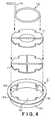
- FIG. 3is an exploded sectional view showing a part of the gas supplying unit of FIG. 1 ;
- FIG. 4is an exploded perspective view showing a part of the gas supplying unit of FIG. 1 ;
- FIG. 5is an enlarged sectional view showing a base member and a temperature-controlling unit of the gas supplying unit of FIG. 1 ;
- FIG. 6is a schematic sectional view showing a state in which a temperature detecting part used in the gas supplying unit of FIG. 1 is embedded in a bottom part of a base plate;
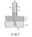
- FIG. 7is a sectional view showing a structure of a distal end of the temperature detecting part of FIG. 6 ;
- FIG. 8is a view of assistance in explaining a relationship between generation of a titanium compound and temperature
- FIG. 9is a structural view showing a temperature controlling system in the gas supplying unit of FIG. 1 ;
- FIG. 10is a schematic sectional view showing a conventional gas supplying unit.
- the gas supplying unit in this embodimentis included in a film-forming apparatus that forms a film by a plasma CVD process.
- a processing container 2is a vacuum chamber made of, e.g., aluminum.
- An upper part of the processing container 2is a cylindrical part 2 a of a larger diameter, and a lower part of the processing container 2 is a cylindrical part 2 b of a smaller diameter.
- the cylindrical parts 2 a and 2 bare continuously connected to form a mushroom shape in general.
- a heating mechanismnot shown, is provided for heating an inner wall of the processing container 2 .
- a stage 21is arranged in the processing container 2 for horizontally placing thereon a substrate such as a semiconductor wafer (hereinafter referred to as “wafer”) W.
- the stage 21is supported on a bottom part of the smaller-diameter part 2 b via a support member 22 .
- a heater 21 a(see, FIG. 2 ) as means for controlling a temperature of the wafer W is arranged in the stage 21 .
- a conductive member(not shown) serving as a lower electrode, which is described below, is arranged in the stage 21 .
- a not-shown electrostatic chuck for electrostatically absorbing the wafer Wis arranged when needed.
- a plurality of, e.g., three support pins 23 for supporting and vertically moving the wafer Wis arranged in the stage 21 .
- the support pins 23are capable of projecting and retracting from a surface of the stage 21 .
- the support pins 23are connected to an elevating mechanism 25 disposed outside the processing container 2 via a support member 24 .
- An discharging pipe 26is connected to a bottom part of the processing container 2 .
- a vacuum pump 27 as vacuum discharging meansis connected to the other end of the discharging pipe 26 .
- a feed port 29which is opened and closed by a gate valve 28 , is formed in a side wall of the larger-diameter part 2 a of the processing container 2 .
- An opening 31is formed at a ceiling part of the processing container 2 .
- a gas showerhead 4 as a gas supplying unit in this embodimentis arranged in such a manner that the gas showerhead 4 hermetically fits in the opening 31 , and is opposed to the stage 21 .
- the gas showerhead 4 and the stage 21serve also as an upper electrode and a lower electrode, respectively. That is, the gas showerhead 4 is connected to a radiofrequency power source 33 through a matching unit 32 , and the stage 21 as the lower electrode is grounded.
- a wiring diagramis schematically illustrated in FIG. 1 , the stage 21 is actually, electrically connected to the processing container 2 , and is grounded through an upper part of the processing container 2 and a matching box, not shown.
- a radiofrequency conductive pathis formed to enclose the processing space.
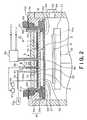
- the gas showerhead 4includes a base member 5 as an upper part and a shower-plate 6 as a lower part.
- the base member 5is formed into a low and large cylindrical shape having a bottom, with its upper surface being opened while its lower surface being closed (in other words, into a circular plate with its peripheral vertically-standing wall).
- An upper end of the peripheral side wall of the cylindrical partis bent outward to form a flange portion 51 .
- An insulating member 34is disposed at an inner peripheral portion of the opening 31 of the processing container 2 . The insulating member 34 prevents passage of electricity (of radiofrequency) from the gas showerhead 4 as the upper electrode to a metal body part of the processing container 2 .
- the flange portion 51 of the base member 5is fixed on an upper surface of the insulating member 34 by a screw, not shown.
- an O-ring 35which is a resin sealing member of a ring shape, is sealingly fitted in a ring-shaped groove formed in the upper surface of the insulating member 34 , and a lower surface of the flange portion 51 and the upper surface of the insulating member 34 are hermetically secured to each other via the O-ring 35 .
- the flange portion 51is secured on the insulating material 34 by the screw at a location outside the O-ring 35 .
- a pushing ring member 36made of an insulating material is disposed to urge the flange portion 51 onto the insulating member 34 . In this manner, the base member 5 hermetically fits in the opening 31 .
- the insulating member 34is of a two-layer structure including an upper part (upper insulating member) 34 a and a lower part (lower insulating member) 34 b .
- a material of the upper part 34 ais alumina, while a material of the lower part 34 b is quartz.
- the lower part 34 bis provided so as to cover a portion of the processing container 2 located laterally adjacent to the base member 5 .
- the reason for adopting the two-layer structureis as follows: That is, since the lower part 34 b covering the showerhead 4 is made of quartz having a low relative dielectric constant, a radiofrequency impedance between the showerhead 4 and a wall of the processing container 2 can be increased as much as possible.
- the upper part 34 ais made of alumina which is easy to be processed, although its relative dielectric constant is high. This makes it easier to bore a threaded opening used for securing the flange portion 51 of the showerhead 4 . That is, the upper part 34 a is formed over a range in which the threaded opening is bored.
- a lower end position of the upper part 34 ai.e., an upper end position of the lower part 34 b , stand as high as possible, so as to enlarge an area of the lower part 34 b covering the showerhead 4 .
- the flange portion 51 and a bottom part 52 of the base member 5are formed of a nickel member.
- nickel memberincludes both a member made of 100% nickel, and a member which is made mainly of nickel but includes some components other than nickel.
- a side wall 53 of the base member 5is made of a material having a lower thermal conductivity than the nickel member. For example, hastelloy is used in this example.
- the side wall 53may conduct upward heat, which is generated for heating a part of the gas showerhead 4 on a side of the processing atmosphere (on a side of the process gas). In order to prevent this heat conduction, a thickness of the side wall 53 is reduced to, e.g., 1 mm.
- hastelloyhas a high strength in addition to a low thermal conductivity.
- the thickness of the side wall 53can be reduced, with retaining a strength equivalent to the nickel member.
- due to the vacuum atmosphere within the processing container 2a significantly large force is applied to the side wall 53 .
- the side wall 53is reinforced to prevent a deformation thereof.
- a plurality of, e.g., four projections 54 projecting inward the base member 5is circumferentially provided at equal spaced intervals on an inner periphery of an upper end of the base member 5 .
- Struts 55 as reinforcing memberssuch as reinforcing pipes are arranged so as to connect the respective projections 54 to the bottom part 52 of the base member 5 .
- the projections 54 and the struts 55may conduct heat upward from below.
- the projections 54 and the struts 55are made of a material having a lower thermal conductivity than the nickel member, such as hastelloy. In order to combine a member made of hastelloy with the nickel member, the members are brazed, for example.
- An air-cooling way 51 a as a coolant way serving as a cooling mechanismis formed in the flange portion 51 to prevent a temperature elevation of the O-ring 35 .
- the shower-plate 6has a circular plate part at a position opposing the stage 21 .
- a peripheral portion surrounding the plate partstands, and an upper part of the standing periphery is bent outward to form a flange portion 60 .
- a portion to be screwedis inwardly cut out from an outer circumference.
- a gas diffusion space 62is formed therebetween.
- a large number of gas-supplying holes 61 for supplying a process gas into the processing container 2is drilled in the shower-plate 6 .
- the gas-supplying holes 61are in communication with the diffusion space 62 .
- the shower-plate 6is formed of the above-described nickel member. As shown in FIGS. 2 and 3 , an upper surface of the flange portion 60 and a lower surface of a peripheral portion of the bottom part 52 of the base plate (base member) 5 are fixed to each other by screws 64 , with a ring-shaped intermediate member 63 being interposed therebetween. A material of the intermediate member 63 is different from the nickel member in order to prevent “sticking” of the nickel members. Specifically, a material which will not cause a metal contamination is preferred. Hastelloy or carbon can be taken for instance. In this example, the intermediate member 63 is made of hastelloy and has a thickness of 2.6 mm.
- the gas showerhead 4 in this embodimentsupplies a mixed gas as a process gas into the processing container 2 .
- the mixed gasis formed in advance by mixing a plurality of gases. That is, the gas supplying unit in this embodiment is of so-called pre-mix type.
- a gas feed port 56 for supplying a process gas (mixed gas)is drilled in a center part of the bottom part 52 of the base member 5 .
- a gas feed pipe 57is extended upward from the gas feed port 56 .
- a gas mixing part 58is connected to an upstream end of the gas feed pipe 57 .
- the gas mixing part 58is connected to, e.g., a TiCl 4 gas source 102 , an Ar gas source 103 , and a CIF 3 gas source 104 , via gas supplying channels 101 .
- the gas mixing part 58is also connected to, e.g., an H 2 gas source 106 and an NH 3 gas source 107 , via gas supplying channels 105 .
- a part 108 encircled with chain linesdepicts a group of gas supplying instruments, such as valves and massflow controllers, disposed on the respective gas supplying channels.
- a temperature adjusting mechanismis arranged above the bottom part 52 of the base member 5 , for adjusting a temperature of the shower-plate 6 facing the gas diffusion space 62 and the processing atmosphere.
- the temperature adjusting mechanismis described with reference to FIG. 4 .
- An insulating plate 7 with a thickness of, e.g., 4 mm made of an insulating member such as aluminum nitride (AlN)is disposed on an upper surface of the bottom part 52 .
- a sheet-like heater 71is placed on the insulating plate 7 .
- the insulating plate 7 and the heater 71are preferably divided into a plurality of elements in a planar direction thereof.
- the sheet heater 71 in this exampleis of a sandwich structure. Namely, protective plates 73 and 74 made of mica as an insulating material sandwich therebetween a core plate 72 made of mica around which a resistive heating line 72 a winds.
- a center of the base member 5 and a center of the heater 71correspond to each other, and that a surface area of the heater 71 relative to a surface area of the base member 5 be 80% or more.
- the insulating plate 7 made of AlNBy interposing the insulating plate 7 made of AlN between the base member 5 and the heater 71 , when a plasma process is conducted, the influence given on the heater 71 by the radiofrequency flowing through the base member 5 can be reduced. Thus, dielectric breakdown of mica of the heater 71 can be prevented. Moreover, since AlN has a high thermal conductivity, it can be expected that heat is efficiently transmitted from the heater 71 to the base member 5 .
- an air-cooling pipe 75 as a cooling mechanismis disposed on the upper surface of the heater 71 .
- the air-cooling pipe 75includes an annular ring portion, and an airline 76 standing from the ring portion. A proximal end of the airline 76 is connected to an air source 76 a .
- a large number of blowing holes 77 and 78 for blowing an air of, e.g., normal temperatureis formed at spaced intervals in a lower side surface of the ring portion of the air-cooling pipe 75 in a length direction (circumferential direction) thereof.
- the blowing holes 77are oriented inward at an angle of 45° relative to the vertical line, and the blowing holes 78 are oriented outward at an angle of 45° relative to the vertical line.
- a cooling operation by the air blown from the blowing holes 77 and 78is performed between a film-forming process and a cleaning process, so as to rapidly cool the bottom part 52 of the base member 5 .
- the cooling operationcan be performed when a detected temperature of the bottom part 52 exceeds a set temperature because of radiant heat from the stage 21 during a process such as a pre-coating process.
- the air blown from the blowing holes 77cools a center region of the heater 71
- the air blown from the blowing holes 78cools a peripheral region of the heater 71 .
- a size (diameter) of the ring portion of the air-cooling pipe 75can be suitably decided based on experiments or the like.
- the temperature detecting part 8includes a sheath metal 81 filled with magnesia (magnesium oxide) 82 as an insulating material, and a thermocouple 83 inserted in the sheath metal 81 .
- a distal end of the sheath metal 81is covered with a protective cap 84 made of alumina as an insulating material.
- the temperature detecting part 8passes through respective openings formed in the heater 71 , the insulating plate 7 , and the bottom part 52 of the base member 5 to be embedded in the bottom part 52 (see, FIG. 2 ).
- a protective tube 85stands from the heater 71 to receive therein parts of the sheath metal 81 and the protective cap 84 .
- An upper part of the sheath metal 81is fixed on the base member 5 via a fixing member 86 (see, FIG. 2 ).
- the reference numbers 87 and 88depict a controlling part and a power source part, respectively.
- the controlling part 87performs a temperature control by adjusting a power supplied from the power source part 88 to the heater 71 , based on a detected temperature value detected by the temperature detecting part 8 .
- the reference number 88 adepicts a feeder wire.
- the protective cap 84may be made of AlN. However, because of its high dielectric constant, AlN may have a large amount of heat generated by induction heating. When a temperature is elevated by the amount of heat, the elevation may have an adverse effect on the detected temperature value, which may make unstable the temperature control. For this reason, a preferable material of the protective cap 84 is alumina. Since alumina has a low dielectric constant, an amount of heat generated by induction heating is also small. As a result, accurate and stable temperature control can be achieved.
- the processing container 2Before the wafer W is processed, the processing container 2 is subjected to a pre-coating process.
- the pre-coating processis conducted for forming, on surfaces of members to be exposed to a processing atmosphere (process gas), a film which is the same kind as a film to be formed on the wafer W.
- the pre-coating processis a Ti-film forming process.
- a mixed gas of TiCl 4 gas and an Ar gasis supplied as a first gas from the gas supplying sources 102 and 103 into the gas mixing part 58 via the gas supplying channels 101 .
- An H 2 gas as a second gasis supplied from the gas supplying source 106 into the gas mixing part 58 via the gas supplying channel 105 .
- These gasesare mixed in the gas mixing part 58 .
- the mixed gasis discharged to the diffusion space 62 in the gas showerhead 4 via the gas inlet pipe 57 , and is diffused in the diffusion space 62 . Then, the gas is supplied into the processing container 2 via the gas supplying-holes 61 of the shower-plate 6 .
- the interior of the processing container 2is evacuated to create a vacuum therein by the vacuum pump 27 . That is, a pressure adjusting valve, not shown, disposed on the discharging pipe 26 is adjusted to adjust a pressure in the processing container 2 to a set pressure.
- a radiofrequency poweris applied by the radiofrequency power source 33 between the gas showerhead 4 as an upper electrode and the stage 21 as a lower electrode.
- the process gasis made plasma, and TiCl 4 is reduced by H 2 .
- a Ti filmis deposited (pre-coat film is formed) on the surfaces of the members in contact with the processing atmosphere, more precisely, the upper surface of the stage 21 and the lower surface of the shower-plate 6 .
- HCl as a reaction byproductis discharged along with a non-reacted gas.
- a temperature of the shower-plate 6has to be set at a predetermined set temperature of, e.g., 420° C.
- the temperature of the stage 21is set at 650° C., for example, and a temperature of the gas showerhead 4 is raised by radiant heat from the stage 21 .
- the temperature of the gas showerhead 4is controlled in the following manner. That is, air is constantly blown to keep the temperature of the overall gas showerhead 4 lower than the set temperature of 420° C. Under this state, the heater 71 is operated to heat the gas showerhead 4 so as to conform a detected temperature value to the set temperature value.
- the air-blowing operationis used for adjusting a temperature of the gas showerhead 4 to conform to the set temperature, it is difficult to stably control the temperature, because of its slow change of endothermic amount.
- the heater 71since the heater 71 is used to conform the temperature of the gas showerhead 4 to the set temperature, the temperature control thereof can be stably carried out. Consequently, an excellent pre-coating process can be realized.
- the wafer W as a substrateis loaded into the processing container 2 by a conveying arm, not shown, through the feed port 29 opened by the gate valve 28 .
- the wafer Wis delivered to the stage 21 by the support pins 23 .
- the gate valve 28is closed.
- the film forming processis conducted. Therefore, a Ti film is formed on the wafer W.
- the temperature of the gas showerhead 4is controlled in a manner similar to the above pre-coating process.
- the supply of the TiCl 4 gas as the first gas and the H 2 gas as the second gasis stopped, and the supply of an NH 3 (ammonia) gas is started.
- the NH 3 gasis discharged into the gas diffusion space 62 , and the diffused NH 3 gas is discharged into the process space through the gas-supplying holes 61 .
- a radiofrequency poweris supplied to the process space.
- a surface of the Ti film already formed on the wafer Wis nitrided by active species of NH 3 .
- the supply of the radiofrequency power and the supply of the NH 3 gasare stopped. Subsequently, the wafer W is unloaded from the processing container 2 in accordance with the procedures reverse to the loading operation.
- a cleaning processis conducted.
- the cleaning processis conducted by supplying a CIF 3 gas, which is not made plasma, from the showerhead 4 into the processing container 2 via the gas supplying channel 101 .
- the temperature of the shower-plate 6has to be set at about 200 to 250° C. Since the air is constantly blown from the air-cooling pipe 75 , the gas showerhead 4 is rapidly cooled by a cooling operation of the blowing air when the heater 71 is turned off. Thus, it is possible to promptly put the cleaning operation into practice.
- the ring-shaped intermediate member 63 made of hastelloyis disposed between the upper surface of the peripheral portion of the shower-plate 6 and the lower surface of the peripheral portion of the base member 5 , in order to prevent sticking of the shower-plate 6 and the base member 5 .
- the sticking phenomenon of the nickel memberswhich might be caused by a high temperature, can be prevented.
- the gas showerhead 4can be easily disassembled for a maintenance operation thereof, the operator can clean or inspect the inside of the gas showerhead without any trouble. That is, replacement of some members can be avoided, which might be necessary if the maintenance operation cannot be performed. This restrains increase in running costs.
- the side wall 53 and the struts 55 as reinforcing members of the base member 5out of hastelloy having a low thermal conductivity, escape of heat outward from the bottom part 52 of the base member 5 can be reduced.
- the shower-plate 6can be efficiently heated, so that the power consumption can be saved.
- a thickness of the side wall 53can be reduced as thin as 1 mm. This also can moderate the escape of heat from the bottom part 52 of the base member 5 to outside, and save the power consumption.
- the temperature controlis conducted by a controlling part 9 (see, FIG. 9 ). That is, the controlling part 9 controls instruments for the air-blowing operation as well as the heater 71 .
- the heater 71is placed on the insulating plate 7 made of AlN, a dielectric breakdown of the heater 71 will not occur. Furthermore, since the distal end of the temperature detecting part 8 is covered with the alumina cap 84 , a stable temperature control can be practiced.
- the film forming processis conducted to the wafer W by using the above film forming apparatus as a substrate processing apparatus, it is general to prepare a plurality of set temperatures of the wafer W, depending on a kind of completed integrated circuit or a part on which a film is formed.
- a plurality of process stepsis continuously performed, for example, when a Ti film is formed by using the TiCl 4 gas and the H 2 gas, and the Ti film is subsequently nitrided by the NH 3 gas, attention has to be paid to a temperature of a part in contact with the processing atmosphere of the gas showerhead 4 (this temperature is referred to as “temperature of the shower-plate 6 ”).
- the TiClxadheres to a part of a low temperature in the processing container, and makes unstable the film forming process.
- the TiClxadheres to the shower-plate 6 in contact with the plasma and remains thereon in an unstable state, there is a possibility that unnecessary Ti atoms are supplied to the plasma during the Ti-film forming process so as to significantly deteriorate reproductivity of the Ti-film forming process.
- the decomposition (stabilization) temperature of the TiClxis more than about 400° C., although it depends on the nitride process succeeding the Ti-film forming process.
- FIG. 8shows a relationship between the temperature and the compound, in which a decomposition temperature of TiClx, a generation temperature of the nickel compound, and a sublimation temperature of the nickel compound are represented by TA, TB, and TC, respectively.
- the temperature of the shower-plate 6is required to be lower than the generation temperature TB of the nickel compound, or higher than the sublimation temperature TC thereof. In this case, from the standpoint of a safe and reliable system that does not allow generation of the nickel compound itself, the temperature of the shower-plate 6 is preferred to be lower than the generation temperature TB of the nickel compound.
- a temperature of the shower-plate 6when a temperature of the wafer W is lower than the sublimation temperature TC of the nickel compound, a temperature of the shower-plate 6 must be inevitably lower than TB. This is because, even when the nickel compound is sublimated by increasing the temperature of the shower-plate 6 higher than TC, the sublimate may adhere to the surface of the wafer W.
- the process recipemay be stored in a storage unit 91 in the controlling part 9 as a temperature table (see, FIG. 9 ).
- a temperature tablesee, FIG. 9 .
- a temperature of the wafer, a temperature of the shower-plate 6 (shower temperature), and a temperature of the heater 71can be set as follows: Wafer Temperature Shower Temperature of Heater 71 (° C.) Temperature (° C.) (° C.) 450 400 400 450 450 475 550 400 320 550 410 600 400 180 600 450 300
- the gas showerhead according to the present inventionis not limited to the pre-mix type, and may be of the conventional post-mix type as shown in FIG. 10 . That is, the present invention can be applied to any apparatus in which a first gas and a second gas are separately supplied to the processing container 2 .
- the present inventioncan be applied to any gas process such as a film forming process conducted at a high temperature for manufacturing a semiconductor device, including: a process for forming a film made out of a metal such as W, Cu, Ta, Ru, and Hf; a process for forming a film out of a metal compound such as TiN, TiSi, and WSi; and a process for forming a film out of an insulating material such as SiN and SiO 2 , for example.
- a gas processsuch as a film forming process conducted at a high temperature for manufacturing a semiconductor device, including: a process for forming a film made out of a metal such as W, Cu, Ta, Ru, and Hf; a process for forming a film out of a metal compound such as TiN, TiSi, and WSi; and a process for forming a film out of an insulating material such as SiN and SiO 2 , for example.
- the gas showerhead according to the present inventioncan be applied to other substrate processing apparatuses such as a thermal CVD apparatus, etching apparatus, ashing apparatus, spattering apparatus, and annealing apparatus.
- a semiconductor waferis used as a substrate
- an LCD substrate and a glass substratemay be used.
- the joining portions of the nickel membersare not limited to the above embodiment.
- an intermediate membermay be interposed between their joining surfaces. That is, the present invention can be applied to any gas supplying unit formed by combining a plurality of nickel members.
Landscapes
- Chemical & Material Sciences (AREA)
- Engineering & Computer Science (AREA)
- Physics & Mathematics (AREA)
- Materials Engineering (AREA)
- Chemical Kinetics & Catalysis (AREA)
- Mechanical Engineering (AREA)
- Metallurgy (AREA)
- Organic Chemistry (AREA)
- General Chemical & Material Sciences (AREA)
- Plasma & Fusion (AREA)
- Analytical Chemistry (AREA)
- Condensed Matter Physics & Semiconductors (AREA)
- General Physics & Mathematics (AREA)
- Manufacturing & Machinery (AREA)
- Computer Hardware Design (AREA)
- Microelectronics & Electronic Packaging (AREA)
- Power Engineering (AREA)
- Chemical Vapour Deposition (AREA)
Abstract
Description
- This invention relates to a gas supplying unit that supplies a process gas into a processing container from a large number of gas-supplying holes opposite to a substrate, in order to conduct a predetermined film-forming process to the substrate, and to a substrate processing apparatus including the gas supplying unit.
- The film-forming process is one of the semiconductor manufacturing processes. The film-forming process is generally conducted by, e.g., under a vacuum atmosphere, ionizing a process gas to form a plasma thereof or pyrolytically decomposing the process gas to activate the process gas, and depositing active species or reaction products on a surface of a substrate. There is a film-forming process in which a variety of gases are reacted on each other to form a film. For example, a thin film is formed of a metal such as Ti, Cu, and Ta, or a metal compound such as TiN, TiSi, and WSi, or an insulating material such as SiN and SiO2.
- An apparatus for conducing the film-forming process includes a stage for placing a substrate thereon, the stage being provided in a processing container which is a vacuum chamber, and a gas supplying unit provided in the processing container. Further, a heater, a plasma generating unit, and so on are provided for energizing the gas.
- The gas supplying unit, which is generally referred to as a gas showerhead, is arranged to hermetically fit in an opening formed at a ceiling part of the processing container so as to be opposed to the stage. The gas showerhead is described in JP2002-327274A, for example. Specifically, as shown in
FIG. 10 , the gas showerhead includes: abase member 11 of a low and large cylindrical shape having a bottom, which fits in an opening formed at an upper part of a processing container; and a shower-plate 12 arranged on a lower side of a bottom surface of thebase member 11. Thebase member 11 also functions as a separator for separating a vacuum atmosphere within the processing container from the atmospheric air. Thus, aflange portion 13 at an upper peripheral portion of thebase member 11 and aperipheral portion 14 of the opening of the processing container are hermetically joined to each other via an O-ring 15 which is a ring-shaped sealing member made of resin. - A standing side wall is provided at a peripheral portion of the shower-
plate 12. An upper edge of the side wall serves as aflange portion 12a. Theflange portion 12aand a peripheral portion of a bottom part15aof thebase member 11 are joined to each other by abolt 16. Two gas-supplying pipes17aand17bare connected to a center part of thebase member 11. Gases supplied from the gas-supplying pipes17aand17bare respectively jetted through gas-supplyingholes plate 12. - Nickel is used as a material for the gas showerhead. This is because: the nickel gas showerhead has a high corrosion resistance under a high temperature such as about 500° C.; a substrate is hardly suffered from a metal contamination from the nickel gas showerhead; and when a plasma process is conducted, the nickel gas showerhead also servers as an electrode with a high conductivity.
- However, such a gas showerhead has the following disadvantages.
- That is, depending on a kind of a process, a temperature of the showerhead may be raised to, e.g., 420° C. or higher, because of a high temperature of the processing atmosphere. Such a high temperature may cause “sticking” of the shower-
plate 12 and thebase member 11 at their joining portions. As described below, the experiment shows that a temperature of 450° C. or higher results in tight “sticking” phenomenon. That is, when the gas showerhead is used at a temperature of 420° C. or higher, there might be concern that the “sticking” phenomenon occurs, depending on manners of the usages and conditions of the joining surfaces. In a maintenance operation of the unit, the showerhead is disassembled for cleaning its inside space. However, when the sticking phenomenon has occurred, it is impossible to separate the shower-plate 12 and thebase member 11 from each other, or a large force is required therefor. The sticking phenomenon is caused by that surface atoms of the nickel material diffuse through a joining interface, while the joining surfaces are stuck to each other by an anchor effect because of minute roughness in the joining surfaces. As described above, the sticking phenomenon makes difficult the maintenance operation. Alternatively, these members have to be periodically replaced. This replacement increases running costs, since the gas showerhead is made of a nickel material. - In addition, due to a large thermal conductivity of nickel, a heat quantity released through the side wall of the
base member 11 is large. Thus, a calorific value of a heater provided in the gas showerhead should be increased. This is disadvantageous in that a power consumption is increased and the O-ring 15 is deteriorated because of the elevated temperature. Provision of a cooling mechanism can prevent the deterioration of the O-ring 15. However, since a large amount of heat is released from thebase member 11, a large amount of consumption energy is required for cooling. - Moreover, the above gas showerhead has the following problem.
- That is, in order to control a temperature of the gas showerhead, a sheet-like heater is arranged on an upper side of the bottom part of the
base member 11. Also, a temperature detecting part having a thermocouple is arranged, with a distal end of the thermocouple being embedded in the bottom part of thebase member 11. Based on a temperature value detected by the temperature detecting part, electric power to be supplied to the sheet heater can be controlled. The temperature detecting part is structured by inserting the thermocouple in a sheath metal filled with an insulating material. When a plasma process is conducted, there might be a possibility that a radiofrequency from the gas showerhead is applied between the sheath metal and the thermocouple to invite a dielectric breakdown. In order to prevent such a situation, an insulating material is sometimes provided between thebase member 11 and the temperature detecting part. This, in turn, may make unstable the temperature control, because a heat generated by induction heating of the insulating material affects the detected temperature value. - This invention is intended to solve the above problems. The object of this invention is to provide a gas supplying unit for supplying a process gas into a processing container, that is capable of preventing sticking of nickel members under a high temperature, so as to improve a maintenance property of the unit. Another object of the present invention is to provide a substrate processing apparatus including the gas supplying unit.
- In order to achieve the above object, the present invention is a gas supplying unit to be arranged to hermetically fit in an opening formed at a ceiling part of a processing container for conducting a process to a substrate: the gas supplying unit comprising a plurality of nickel members, wherein a large number of gas-supplying holes is formed at a lower surface of the gas supplying unit, a process gas is adapted to be supplied from the large number of gas-supplying holes into the processing container, and the plurality of nickel members is fixed to each other via an intermediate member for preventing sticking made of a material different from nickel.
- According to the present invention, between the joining surfaces of the plurality of nickel members, there is provided the intermediate member for preventing sticking made of a material different from nickel. Thus, the nickel portions are prevented from sticking to each other which might be caused by a high temperature. Since the gas showerhead can be easily disassembled for a maintenance operation, it is easy to clean and inspect an inside thereof. That is, replacement of the members can be avoided, which might be necessary when the maintenance operation cannot be performed.
- Alternatively, the present invention is a gas supplying unit to be arranged to hermetically fit in an opening formed at a ceiling part of a processing container for conducting a process to a substrate: the gas supplying unit comprising a shower-plate mainly consisting of nickel, a large number of gas-supplying holes being formed in the shower-plate, and a base member provided above the shower-plate in order to form a process-gas diffusion space between the base member and the shower-plate, wherein a portion of the base member opposite to the shower-plate is made mainly of nickel, and an upper surface of a peripheral portion of the shower-plate and a lower surface of a peripheral portion of the base member are hermetically fixed to each other via an intermediate member for preventing sticking made of a material different from nickel.
- According to the present invention, between the upper surface of a peripheral portion of the shower-plate and the lower surface of a peripheral portion of the base member, there is provided the intermediate member for preventing sticking made of a material different from nickel. Thus, the nickel members are prevented from sticking to each other which might be caused by a high temperature. Since the gas showerhead can be easily disassembled for a maintenance operation, it is easy to clean and inspect an inside thereof. That is, replacement of the members can be avoided, which might be necessary when the maintenance operation cannot be performed.
- The term “nickel member” (or “nickel portion”) is not limited to a member (or portion) made of 100% nickel, but includes a member (or portion) made mainly of nickel.
- Hastelloy or carbon are given as an example of a material of the intermediate member.
- For example, the base member may be formed into a low and large cylindrical shape having a bottom, an upper end of a peripheral side wall of the base member may be hermetically attached to a peripheral portion of the opening of the processing container, and a bottom surface of the peripheral side wall of the base member may be hermetically fixed to a peripheral portion of the shower-plate. In this case, the peripheral side wall of the base member may be made of a material having a lower thermal conductivity than nickel. The material is preferably hastelloy. In addition, it is preferable that the base member may be provided with a reinforcement member made of a material having a lower thermal conductivity than nickel, in order to reinforce the peripheral side wall of the base member. Further, it is preferable that a coolant way be formed at an upper-end portion of the peripheral side wall of the base member.
- In addition, preferably, a sheet-like heater is arranged on the base member via an insulating plate, the insulating plate is divided into a plurality of insulating-plate elements in a planar direction thereof, and the sheet-like heater is divided into a plurality of sheet-heater elements in a planar direction thereof.
- In addition, for example, the process gas may include a first gas and a second gas, the first gas and the second gas may be capable of reacting on each other in order to generate a film-forming component, the first gas and the second gas may be mixed in advance to become a mixed gas, and the mixed gas may be supplied into the processing container as a process gas (so-called pre-mix type of gas supply).
- In addition, the present invention is a substrate processing apparatus comprising a processing container whose ceiling part has an opening, a stage provided in the processing container, for placing a substrate thereon, a gas discharging unit for discharging a gas from the processing container, and a gas supplying unit arranged to hermetically fit in the opening of the ceiling part of the processing container, wherein the gas supplying unit comprises a plurality of nickel members, a large number of gas-supplying holes is formed at a lower surface of the gas supplying unit, a process gas is adapted to be supplied from the large number of gas-supplying holes into the processing container, and the plurality of nickel members is fixed to each other via an intermediate member for preventing sticking made of a material different from nickel.
- Alternatively, the present invention is a substrate processing apparatus comprising a processing container whose ceiling part has an opening, a stage provided in the processing container, for placing a substrate thereon, a gas discharging unit for discharging a gas from the processing container, and a gas supplying unit arranged to hermetically fit in the opening of the ceiling part of the processing container, wherein the gas supplying unit comprises: a shower-plate mainly consisting of nickel, a large number of gas-supplying holes being formed in the shower-plate; and a base member provided above the shower-plate in order to form a process-gas diffusion space between the base member and the shower-plate, a portion of the base member opposite to the shower-plate is made mainly of nickel, and an upper surface of a peripheral portion of the shower-plate and a lower surface of a peripheral portion of the base member are hermetically fixed to each other via an intermediate member for preventing sticking made of a material different from nickel.
- In this case, for example, the base member may be formed into a low and large cylindrical shape having a bottom, an upper end of a peripheral side wall of the base member may be hermetically attached to a peripheral portion of the opening of the processing container, and a bottom surface of the peripheral side wall of the base member may be hermetically fixed to a peripheral portion of the shower-plate.
- In this case, preferably, the upper end of the peripheral side wall of the base member may be hermetically attached to the peripheral portion of the opening of the processing container via an upper-side insulating member made of alumina for radio-frequency insulation, and a lower-side insulating member made of quartz for radio-frequency insulation may be provided below the upper-side insulating member so as to cover a portion of the processing container located laterally adjacent to the peripheral side wall of the base member.
- Alternatively, preferably, the upper end of the peripheral side wall of the base member may be hermetically attached to the peripheral portion of the opening of the processing container via a sealing member made of resin.
- In addition, for example, the substrate processing apparatus may further comprise a first temperature-controlling unit provided in the stage for heating the substrate, a second temperature-controlling unit provided in the gas supplying unit for controlling a temperature of a surface of the gas supplying unit in contact with the process gas, and a controlling part that controls the first temperature-controlling unit and the second temperature-controlling unit, wherein a gas supplying control is adapted to be conducted in such a manner that: a titanium chloride gas and a hydrogen gas are supplied as a process gas from the gas supplying unit into the processing container in order to generate a titanium film on the substrate, and then an ammonia gas is supplied from the gas supplying unit into the processing container in order to nitride the titanium film on the substrate, and the controlling part is adapted to control the second temperature-controlling unit in such a manner that: a temperature of the surface of the gas supplying unit in contact with the process gas is lower than a temperature at which nickel and ammonia react to generate a solid product, and is within a decomposition temperature zone of TiClx (x=1, 2 or 3).
- In this case, for example, the controlling part may be adapted to control the second temperature-controlling unit in such a manner that a temperature of the surface of the gas supplying unit in contact with the process gas is 400 to 450° C.
- Alternatively, for example, the controlling part may be adapted to control the first temperature-controlling unit in such a manner that a temperature of the substrate is increased to 450 to 600° C., and the controlling part may be adapted to control the second temperature-controlling unit in such a manner that a temperature of the second temperature-controlling unit is 180 to 475° C. depending on the temperature of the substrate.
FIG. 1 is a schematic sectional view of a film-forming apparatus including a gas supplying unit according to an embodiment of the present invention;FIG. 2 is a schematic sectional view showing the gas supplying unit ofFIG. 1 in details;FIG. 3 is an exploded sectional view showing a part of the gas supplying unit ofFIG. 1 ;FIG. 4 is an exploded perspective view showing a part of the gas supplying unit ofFIG. 1 ;FIG. 5 is an enlarged sectional view showing a base member and a temperature-controlling unit of the gas supplying unit ofFIG. 1 ;FIG. 6 is a schematic sectional view showing a state in which a temperature detecting part used in the gas supplying unit ofFIG. 1 is embedded in a bottom part of a base plate;FIG. 7 is a sectional view showing a structure of a distal end of the temperature detecting part ofFIG. 6 ;FIG. 8 is a view of assistance in explaining a relationship between generation of a titanium compound and temperature;FIG. 9 is a structural view showing a temperature controlling system in the gas supplying unit ofFIG. 1 ; andFIG. 10 is a schematic sectional view showing a conventional gas supplying unit.- An embodiment of the present invention will be described below. The gas supplying unit in this embodiment is included in a film-forming apparatus that forms a film by a plasma CVD process.
- The general structure of the film-forming apparatus is described with reference to the schematic sectional view of FIG.1. In
FIG. 1 , aprocessing container 2 is a vacuum chamber made of, e.g., aluminum. An upper part of theprocessing container 2 is acylindrical part 2aof a larger diameter, and a lower part of theprocessing container 2 is acylindrical part 2bof a smaller diameter. Thecylindrical parts processing container 2. Astage 21 is arranged in theprocessing container 2 for horizontally placing thereon a substrate such as a semiconductor wafer (hereinafter referred to as “wafer”) W. Thestage 21 is supported on a bottom part of the smaller-diameter part 2bvia asupport member 22. - A
heater 21a(see,FIG. 2 ) as means for controlling a temperature of the wafer W is arranged in thestage 21. A conductive member (not shown) serving as a lower electrode, which is described below, is arranged in thestage 21. A not-shown electrostatic chuck for electrostatically absorbing the wafer W is arranged when needed. A plurality of, e.g., threesupport pins 23 for supporting and vertically moving the wafer W is arranged in thestage 21. The support pins23 are capable of projecting and retracting from a surface of thestage 21. The support pins23 are connected to an elevatingmechanism 25 disposed outside theprocessing container 2 via asupport member 24. One end of an dischargingpipe 26 is connected to a bottom part of theprocessing container 2. Avacuum pump 27 as vacuum discharging means is connected to the other end of the dischargingpipe 26. Afeed port 29, which is opened and closed by agate valve 28, is formed in a side wall of the larger-diameter part 2aof theprocessing container 2. - An
opening 31 is formed at a ceiling part of theprocessing container 2. Agas showerhead 4 as a gas supplying unit in this embodiment is arranged in such a manner that thegas showerhead 4 hermetically fits in theopening 31, and is opposed to thestage 21. Thegas showerhead 4 and thestage 21 serve also as an upper electrode and a lower electrode, respectively. That is, thegas showerhead 4 is connected to aradiofrequency power source 33 through amatching unit 32, and thestage 21 as the lower electrode is grounded. Although a wiring diagram is schematically illustrated inFIG. 1 , thestage 21 is actually, electrically connected to theprocessing container 2, and is grounded through an upper part of theprocessing container 2 and a matching box, not shown. A radiofrequency conductive path is formed to enclose the processing space. - As shown in
FIG. 2 , thegas showerhead 4 includes abase member 5 as an upper part and a shower-plate 6 as a lower part. Thebase member 5 is formed into a low and large cylindrical shape having a bottom, with its upper surface being opened while its lower surface being closed (in other words, into a circular plate with its peripheral vertically-standing wall). An upper end of the peripheral side wall of the cylindrical part is bent outward to form aflange portion 51. An insulatingmember 34 is disposed at an inner peripheral portion of theopening 31 of theprocessing container 2. The insulatingmember 34 prevents passage of electricity (of radiofrequency) from thegas showerhead 4 as the upper electrode to a metal body part of theprocessing container 2. Theflange portion 51 of thebase member 5 is fixed on an upper surface of the insulatingmember 34 by a screw, not shown. In more detail, an O-ring 35, which is a resin sealing member of a ring shape, is sealingly fitted in a ring-shaped groove formed in the upper surface of the insulatingmember 34, and a lower surface of theflange portion 51 and the upper surface of the insulatingmember 34 are hermetically secured to each other via the O-ring 35. Theflange portion 51 is secured on the insulatingmaterial 34 by the screw at a location outside the O-ring 35. A pushingring member 36 made of an insulating material is disposed to urge theflange portion 51 onto the insulatingmember 34. In this manner, thebase member 5 hermetically fits in theopening 31. - The insulating
member 34 is of a two-layer structure including an upper part (upper insulating member)34aand a lower part (lower insulating member)34b. A material of theupper part 34ais alumina, while a material of thelower part 34bis quartz. Thelower part 34bis provided so as to cover a portion of theprocessing container 2 located laterally adjacent to thebase member 5. The reason for adopting the two-layer structure is as follows: That is, since thelower part 34bcovering theshowerhead 4 is made of quartz having a low relative dielectric constant, a radiofrequency impedance between theshowerhead 4 and a wall of theprocessing container 2 can be increased as much as possible. Thus, leakage of a radiofrequency from between theshowerhead 4 and theprocessing container 2 can be lowered, which decreases loss of power and leakage of noises, so that abnormal electric discharge hardly occurs. Meanwhile, since quartz is difficult to be processed, theupper part 34ais made of alumina which is easy to be processed, although its relative dielectric constant is high. This makes it easier to bore a threaded opening used for securing theflange portion 51 of theshowerhead 4. That is, theupper part 34ais formed over a range in which the threaded opening is bored. It is preferable that a lower end position of theupper part 34a, i.e., an upper end position of thelower part 34b, stand as high as possible, so as to enlarge an area of thelower part 34bcovering theshowerhead 4. - The
flange portion 51 and abottom part 52 of thebase member 5 are formed of a nickel member. Herein, the term “nickel member” includes both a member made of 100% nickel, and a member which is made mainly of nickel but includes some components other than nickel. Aside wall 53 of thebase member 5 is made of a material having a lower thermal conductivity than the nickel member. For example, hastelloy is used in this example. Theside wall 53 may conduct upward heat, which is generated for heating a part of thegas showerhead 4 on a side of the processing atmosphere (on a side of the process gas). In order to prevent this heat conduction, a thickness of theside wall 53 is reduced to, e.g., 1 mm. Herein, hastelloy has a high strength in addition to a low thermal conductivity. Thus, the thickness of theside wall 53 can be reduced, with retaining a strength equivalent to the nickel member. However, due to the vacuum atmosphere within theprocessing container 2, a significantly large force is applied to theside wall 53. Thus, theside wall 53 is reinforced to prevent a deformation thereof. - That is, as shown in the exploded perspective view of
FIG. 4 , a plurality of, e.g., fourprojections 54 projecting inward thebase member 5 is circumferentially provided at equal spaced intervals on an inner periphery of an upper end of thebase member 5.Struts 55 as reinforcing members such as reinforcing pipes are arranged so as to connect therespective projections 54 to thebottom part 52 of thebase member 5. Theprojections 54 and thestruts 55 may conduct heat upward from below. Thus, in this example, theprojections 54 and thestruts 55 are made of a material having a lower thermal conductivity than the nickel member, such as hastelloy. In order to combine a member made of hastelloy with the nickel member, the members are brazed, for example. - An air-cooling
way 51aas a coolant way serving as a cooling mechanism is formed in theflange portion 51 to prevent a temperature elevation of the O-ring 35. - Next, the shower-
plate 6, which is the lower part of thegas showerhead 4, is described. - The shower-
plate 6 has a circular plate part at a position opposing thestage 21. A peripheral portion surrounding the plate part stands, and an upper part of the standing periphery is bent outward to form aflange portion 60. A portion to be screwed is inwardly cut out from an outer circumference. - By fixing the shower-
plate 6 to thebase member 5, agas diffusion space 62 is formed therebetween. A large number of gas-supplyingholes 61 for supplying a process gas into theprocessing container 2 is drilled in the shower-plate 6. The gas-supplyingholes 61 are in communication with thediffusion space 62. - The shower-
plate 6 is formed of the above-described nickel member. As shown inFIGS. 2 and 3 , an upper surface of theflange portion 60 and a lower surface of a peripheral portion of thebottom part 52 of the base plate (base member)5 are fixed to each other byscrews 64, with a ring-shapedintermediate member 63 being interposed therebetween. A material of theintermediate member 63 is different from the nickel member in order to prevent “sticking” of the nickel members. Specifically, a material which will not cause a metal contamination is preferred. Hastelloy or carbon can be taken for instance. In this example, theintermediate member 63 is made of hastelloy and has a thickness of 2.6 mm. - The
gas showerhead 4 in this embodiment supplies a mixed gas as a process gas into theprocessing container 2. The mixed gas is formed in advance by mixing a plurality of gases. That is, the gas supplying unit in this embodiment is of so-called pre-mix type. As shown inFIG. 2 , agas feed port 56 for supplying a process gas (mixed gas) is drilled in a center part of thebottom part 52 of thebase member 5. Agas feed pipe 57 is extended upward from thegas feed port 56. Agas mixing part 58 is connected to an upstream end of thegas feed pipe 57. Thegas mixing part 58 is connected to, e.g., a TiCl4gas source102, anAr gas source 103, and a CIF3gas source104, viagas supplying channels 101. Thegas mixing part 58 is also connected to, e.g., an H2gas source106 and an NH3gas source107, viagas supplying channels 105. Apart 108 encircled with chain lines depicts a group of gas supplying instruments, such as valves and massflow controllers, disposed on the respective gas supplying channels. - A temperature adjusting mechanism is arranged above the
bottom part 52 of thebase member 5, for adjusting a temperature of the shower-plate 6 facing thegas diffusion space 62 and the processing atmosphere. The temperature adjusting mechanism is described with reference toFIG. 4 . - An insulating
plate 7 with a thickness of, e.g., 4 mm made of an insulating member such as aluminum nitride (AlN) is disposed on an upper surface of thebottom part 52. A sheet-like heater 71 is placed on the insulatingplate 7. From the standpoint of a maintenance property, the insulatingplate 7 and theheater 71 are preferably divided into a plurality of elements in a planar direction thereof. In this example, there are employed the insulatingplate 7 divided into four elements and theheater 71 divided into two elements. As shown inFIG. 5 , thesheet heater 71 in this example is of a sandwich structure. Namely,protective plates core plate 72 made of mica around which aresistive heating line 72awinds. - With a view to stabilizing a temperature of the shower-
plate 6, it is preferable that a center of thebase member 5 and a center of theheater 71 correspond to each other, and that a surface area of theheater 71 relative to a surface area of thebase member 5 be 80% or more. - By interposing the insulating
plate 7 made of AlN between thebase member 5 and theheater 71, when a plasma process is conducted, the influence given on theheater 71 by the radiofrequency flowing through thebase member 5 can be reduced. Thus, dielectric breakdown of mica of theheater 71 can be prevented. Moreover, since AlN has a high thermal conductivity, it can be expected that heat is efficiently transmitted from theheater 71 to thebase member 5. - Further, as shown in
FIGS. 2, 4 , and5, an air-coolingpipe 75 as a cooling mechanism is disposed on the upper surface of theheater 71. The air-coolingpipe 75 includes an annular ring portion, and anairline 76 standing from the ring portion. A proximal end of theairline 76 is connected to anair source 76a. As shown inFIG. 5 , a large number of blowingholes pipe 75 in a length direction (circumferential direction) thereof. The blowing holes77 are oriented inward at an angle of 45° relative to the vertical line, and the blowing holes78 are oriented outward at an angle of 45° relative to the vertical line. A cooling operation by the air blown from the blowing holes77 and78 is performed between a film-forming process and a cleaning process, so as to rapidly cool thebottom part 52 of thebase member 5. Besides, the cooling operation can be performed when a detected temperature of thebottom part 52 exceeds a set temperature because of radiant heat from thestage 21 during a process such as a pre-coating process. The air blown from the blowing holes77 cools a center region of theheater 71, and the air blown from the blowing holes78 cools a peripheral region of theheater 71. A size (diameter) of the ring portion of the air-coolingpipe 75 can be suitably decided based on experiments or the like. - As shown in
FIG. 2 , a distal end of atemperature detecting part 8 having a thermocouple is embedded in thebottom part 52 of thebase member 5. As shown inFIG. 6 , thetemperature detecting part 8 includes asheath metal 81 filled with magnesia (magnesium oxide)82 as an insulating material, and athermocouple 83 inserted in thesheath metal 81. A distal end of thesheath metal 81 is covered with aprotective cap 84 made of alumina as an insulating material. Thetemperature detecting part 8 passes through respective openings formed in theheater 71, the insulatingplate 7, and thebottom part 52 of thebase member 5 to be embedded in the bottom part52 (see,FIG. 2 ). Aprotective tube 85 stands from theheater 71 to receive therein parts of thesheath metal 81 and theprotective cap 84. An upper part of thesheath metal 81 is fixed on thebase member 5 via a fixing member86 (see,FIG. 2 ). InFIG. 2 , thereference numbers part 87 performs a temperature control by adjusting a power supplied from thepower source part 88 to theheater 71, based on a detected temperature value detected by thetemperature detecting part 8. Thereference number 88adepicts a feeder wire. - If the
sheath metal 81 contacts the base member5 (bottom part52), a radiofrequency flowing through thebase member 5 is applied between thesheath metal 81 and thethermocouple 83, so that the magnesia (magnesium oxide) is dielectrically broken. However, due to the provision of theprotective cap 84, such a dielectric breakdown can be avoided. Theprotective cap 84 may be made of AlN. However, because of its high dielectric constant, AlN may have a large amount of heat generated by induction heating. When a temperature is elevated by the amount of heat, the elevation may have an adverse effect on the detected temperature value, which may make unstable the temperature control. For this reason, a preferable material of theprotective cap 84 is alumina. Since alumina has a low dielectric constant, an amount of heat generated by induction heating is also small. As a result, accurate and stable temperature control can be achieved. - Now, effects of the above-described embodiment will be described. Given herein as an example to describe the process is a case in which a Ti film is formed on a surface of a wafer W. The interior of the
processing container 2 is currently cleaned, and the process is going to be conducted. - Before the wafer W is processed, the
processing container 2 is subjected to a pre-coating process. The pre-coating process is conducted for forming, on surfaces of members to be exposed to a processing atmosphere (process gas), a film which is the same kind as a film to be formed on the wafer W. In this example, the pre-coating process is a Ti-film forming process. - To be specific, a mixed gas of TiCl4gas and an Ar gas is supplied as a first gas from the
gas supplying sources gas mixing part 58 via thegas supplying channels 101. An H2gas as a second gas is supplied from thegas supplying source 106 into thegas mixing part 58 via thegas supplying channel 105. These gases are mixed in thegas mixing part 58. The mixed gas is discharged to thediffusion space 62 in thegas showerhead 4 via thegas inlet pipe 57, and is diffused in thediffusion space 62. Then, the gas is supplied into theprocessing container 2 via the gas supplying-holes 61 of the shower-plate 6. - Meanwhile, the interior of the
processing container 2 is evacuated to create a vacuum therein by thevacuum pump 27. That is, a pressure adjusting valve, not shown, disposed on the dischargingpipe 26 is adjusted to adjust a pressure in theprocessing container 2 to a set pressure. A radiofrequency power is applied by theradiofrequency power source 33 between thegas showerhead 4 as an upper electrode and thestage 21 as a lower electrode. Thus, the process gas is made plasma, and TiCl4is reduced by H2. In this manner, a Ti film is deposited (pre-coat film is formed) on the surfaces of the members in contact with the processing atmosphere, more precisely, the upper surface of thestage 21 and the lower surface of the shower-plate 6. At this time, HCl as a reaction byproduct is discharged along with a non-reacted gas. - In order to enhance a film quality of the pre-coat film, i.e., to make the film dense and difficult to be peeled, a temperature of the shower-
plate 6 has to be set at a predetermined set temperature of, e.g., 420° C. The temperature of thestage 21 is set at 650° C., for example, and a temperature of thegas showerhead 4 is raised by radiant heat from thestage 21. As described above, since a part (such as side wall53) of thegas showerhead 4 is made of hastelloy to prevent escape of heat, a large amount of heat is stored in the shower-plate 6 and thebottom part 52 of thebase member 5, which may undesirably increase the temperature of the shower-plate 6 beyond the set temperature of 420° C. Therefore, in order to cool thegas showerhead 4, air is blown from the air-coolingpipe 75 arranged above thebottom part 52. - In this cooling operation, the temperature of the
gas showerhead 4 is controlled in the following manner. That is, air is constantly blown to keep the temperature of theoverall gas showerhead 4 lower than the set temperature of 420° C. Under this state, theheater 71 is operated to heat thegas showerhead 4 so as to conform a detected temperature value to the set temperature value. When the air-blowing operation is used for adjusting a temperature of thegas showerhead 4 to conform to the set temperature, it is difficult to stably control the temperature, because of its slow change of endothermic amount. However, since theheater 71 is used to conform the temperature of thegas showerhead 4 to the set temperature, the temperature control thereof can be stably carried out. Consequently, an excellent pre-coating process can be realized. - After the pre-coating process is completed, as shown in
FIG. 1 , the wafer W as a substrate is loaded into theprocessing container 2 by a conveying arm, not shown, through thefeed port 29 opened by thegate valve 28. The wafer W is delivered to thestage 21 by the support pins23. Then, thegate valve 28 is closed. In accordance with the same procedures as those to form the pre-coat film, the film forming process is conducted. Therefore, a Ti film is formed on the wafer W. During the film forming process, the temperature of thegas showerhead 4 is controlled in a manner similar to the above pre-coating process. - Following thereto, the supply of the TiCl4gas as the first gas and the H2gas as the second gas is stopped, and the supply of an NH3(ammonia) gas is started. The NH3gas is discharged into the
gas diffusion space 62, and the diffused NH3gas is discharged into the process space through the gas-supplyingholes 61. Similarly to the above, a radiofrequency power is supplied to the process space. Thus, a surface of the Ti film already formed on the wafer W is nitrided by active species of NH3. After the surface is nitrided, the supply of the radiofrequency power and the supply of the NH3gas are stopped. Subsequently, the wafer W is unloaded from theprocessing container 2 in accordance with the procedures reverse to the loading operation. - After the predetermined number of wafers W are subjected to the film forming process, a cleaning process is conducted. The cleaning process is conducted by supplying a CIF3gas, which is not made plasma, from the
showerhead 4 into theprocessing container 2 via thegas supplying channel 101. The temperature of the shower-plate 6 has to be set at about 200 to 250° C. Since the air is constantly blown from the air-coolingpipe 75, thegas showerhead 4 is rapidly cooled by a cooling operation of the blowing air when theheater 71 is turned off. Thus, it is possible to promptly put the cleaning operation into practice. - In the above embodiment, the ring-shaped
intermediate member 63 made of hastelloy is disposed between the upper surface of the peripheral portion of the shower-plate 6 and the lower surface of the peripheral portion of thebase member 5, in order to prevent sticking of the shower-plate 6 and thebase member 5. Thus, the sticking phenomenon of the nickel members, which might be caused by a high temperature, can be prevented. Since thegas showerhead 4 can be easily disassembled for a maintenance operation thereof, the operator can clean or inspect the inside of the gas showerhead without any trouble. That is, replacement of some members can be avoided, which might be necessary if the maintenance operation cannot be performed. This restrains increase in running costs. - As described above, by forming the
side wall 53 and thestruts 55 as reinforcing members of thebase member 5 out of hastelloy having a low thermal conductivity, escape of heat outward from thebottom part 52 of thebase member 5 can be reduced. Thus, the shower-plate 6 can be efficiently heated, so that the power consumption can be saved. Owing to a high strength of hastelloy, a thickness of theside wall 53 can be reduced as thin as 1 mm. This also can moderate the escape of heat from thebottom part 52 of thebase member 5 to outside, and save the power consumption. On the other hand, it is necessary to consider an adverse effect of the above structure. That is, a large amount of heat is stored in the shower-plate 6, so that a temperature of thegas showerhead 4 undesirably may exceed the set temperature. However, since the temperature is controlled: by constantly blowing air to maintain the same slightly lower than the set temperature and then by using theheater 71 to correctly adjust the temperature, the temperature can be suitably controlled. The temperature control is conducted by a controlling part9 (see,FIG. 9 ). That is, thecontrolling part 9 controls instruments for the air-blowing operation as well as theheater 71. - Further, as described above, since the
heater 71 is placed on the insulatingplate 7 made of AlN, a dielectric breakdown of theheater 71 will not occur. Furthermore, since the distal end of thetemperature detecting part 8 is covered with thealumina cap 84, a stable temperature control can be practiced. - Next, results of experiments conducted for confirming an effect of the intermediate member are described below.
- In these experiments, square blocks made of nickel members of 34 mm in length and 16 mm in width were used. The blocks were stacked and fastened to each other by a bolt with a torque of about 3 to 5 N-m. These blocks were heated for fifty hours at temperatures of 450° C. and 500° C., respectively. On the other hand, the blocks with a hastelloy laminate having a thickness of 0.15 mm being interposed therebetween were similarly heated. In the respective experiments, a plurality of samples was prepared and heated.
- Experiment results were as follows: Among the directly joined nickel members which had been heated at the temperature of 450° C., some samples required a tensile stress as large as 200 Kgf for separating the nickel members. On the other hand, among the joined nickel members with the intermediate member which had been heated at the temperature of 450° C., some samples exhibited no sticking phenomenon. Although a few samples exhibited sticking phenomenon, it was easy to manually separate the nickel members. Among the joined nickel members with the intermediate member which had been heated at the temperature of 500° C., a few samples at most exhibited negligible sticking phenomenon.
- Accordingly, it was confirmed that the sticking phenomenon of the nickel members which is caused by a high temperature can be effectively prevented by interposing the intermediate member between the nickel members.
- When the film forming process is conducted to the wafer W by using the above film forming apparatus as a substrate processing apparatus, it is general to prepare a plurality of set temperatures of the wafer W, depending on a kind of completed integrated circuit or a part on which a film is formed. When a plurality of process steps is continuously performed, for example, when a Ti film is formed by using the TiCl4gas and the H2gas, and the Ti film is subsequently nitrided by the NH3gas, attention has to be paid to a temperature of a part in contact with the processing atmosphere of the gas showerhead4 (this temperature is referred to as “temperature of the shower-
plate 6”). At first, in the Ti-film forming process, the TiCl4gas is decomposed in plasma, and a decomposed product TiClx of low order (x=1, 2 or 3) is generated. The TiClx adheres to a part of a low temperature in the processing container, and makes unstable the film forming process. In particular, when the TiClx adheres to the shower-plate 6 in contact with the plasma and remains thereon in an unstable state, there is a possibility that unnecessary Ti atoms are supplied to the plasma during the Ti-film forming process so as to significantly deteriorate reproductivity of the Ti-film forming process. In order to avoid this, it is necessary to maintain the temperature of the shower-plate 6 at a temperature high enough to further decompose the adhered TiClx into a Ti film of a stable state. The decomposition (stabilization) temperature of the TiClx is more than about 400° C., although it depends on the nitride process succeeding the Ti-film forming process. - At a temperature around 450° C., nickel forming the
gas showerhead 4 and the NH3gas are reacted to generate a nickel compound which is a solid product. The nickel compound is sublimated at a temperature around 500° C. Thus, the nickel compound adheres to a part whose temperature is within this range.FIG. 8 shows a relationship between the temperature and the compound, in which a decomposition temperature of TiClx, a generation temperature of the nickel compound, and a sublimation temperature of the nickel compound are represented by TA, TB, and TC, respectively. - Based on the reason as described above, employment of three set temperatures of the wafer W, i.e., the set temperatures of 450° C., 550° C., and 600° C. is contemplated by the inventors of the present invention. When the nickel compound is generated to adhere to the shower-
plate 6, the nickel compound may peel therefrom to cause a particle contamination. Thus, the temperature of the shower-plate 6 is required to be lower than the generation temperature TB of the nickel compound, or higher than the sublimation temperature TC thereof. In this case, from the standpoint of a safe and reliable system that does not allow generation of the nickel compound itself, the temperature of the shower-plate 6 is preferred to be lower than the generation temperature TB of the nickel compound. Additionally, when a temperature of the wafer W is lower than the sublimation temperature TC of the nickel compound, a temperature of the shower-plate 6 must be inevitably lower than TB. This is because, even when the nickel compound is sublimated by increasing the temperature of the shower-plate 6 higher than TC, the sublimate may adhere to the surface of the wafer W. - An example of a process recipe contemplated by the inventors is described. The process recipe may be stored in a
storage unit 91 in thecontrolling part 9 as a temperature table (see,FIG. 9 ). Based on the fact that the a decomposition temperature zone of TiClx is 400° C. or more, and that a generation temperature of the nickel compound is higher than 450° C., a temperature of the wafer, a temperature of the shower-plate6 (shower temperature), and a temperature of theheater 71 can be set as follows:Wafer Temperature Shower Temperature of Heater 71 (° C.) Temperature (° C.) (° C.) 450 400 400 450 450 475 550 400 320 550 450 410 600 400 180 600 450 300 - The gas showerhead according to the present invention is not limited to the pre-mix type, and may be of the conventional post-mix type as shown in
FIG. 10 . That is, the present invention can be applied to any apparatus in which a first gas and a second gas are separately supplied to theprocessing container 2. - Not limited to the Ti-film forming process, the present invention can be applied to any gas process such as a film forming process conducted at a high temperature for manufacturing a semiconductor device, including: a process for forming a film made out of a metal such as W, Cu, Ta, Ru, and Hf; a process for forming a film out of a metal compound such as TiN, TiSi, and WSi; and a process for forming a film out of an insulating material such as SiN and SiO2, for example.
- Moreover, not limited to the plasma CVD apparatus, the gas showerhead according to the present invention can be applied to other substrate processing apparatuses such as a thermal CVD apparatus, etching apparatus, ashing apparatus, spattering apparatus, and annealing apparatus.
- In the above embodiment, although a semiconductor wafer is used as a substrate, an LCD substrate and a glass substrate may be used.
- Furthermore, the joining portions of the nickel members are not limited to the above embodiment. For example, when the shower plate is formed by stacking two plates, an intermediate member may be interposed between their joining surfaces. That is, the present invention can be applied to any gas supplying unit formed by combining a plurality of nickel members.
Claims (22)
1. A gas supplying unit to be arranged to hermetically fit in an opening formed at a ceiling part of a processing container for conducting a process to a substrate: the gas supplying unit comprising
a plurality of nickel members,
wherein
a large number of gas-supplying holes is formed at a lower surface of the gas supplying unit,
a process gas is adapted to be supplied from the large number of gas-supplying holes into the processing container, and
the plurality of nickel members is fixed to each other via an intermediate member for preventing sticking made of a material different from nickel.
2. A gas supplying unit to be arranged to hermetically fit in an opening formed at a ceiling part of a processing container for conducting a process to a substrate: the gas supplying unit comprising
a shower-plate mainly consisting of nickel, a large number of gas-supplying holes being formed in the shower-plate, and
a base member provided above the shower-plate in order to form a process-gas diffusion space between the base member and the shower-plate,
wherein
a portion of the base member opposite to the shower-plate is made mainly of nickel, and
an upper surface of a peripheral portion of the shower-plate and a lower surface of a peripheral portion of the base member are hermetically fixed to each other via an intermediate member for preventing sticking made of a material different from nickel.
3. A gas supplying unit according toclaim 2 , wherein
the base member is formed into a low and large cylindrical shape having a bottom,
an upper end of a peripheral side wall of the base member is hermetically attached to a peripheral portion of the opening of the processing container, and
a bottom surface of the peripheral side wall of the base member is hermetically fixed to a peripheral portion of the shower-plate.
4. A gas supplying unit according toclaim 3 , wherein
the peripheral side wall of the base member is made of a material having a lower thermal conductivity than nickel.
5. A gas supplying unit according toclaim 4 , wherein
the base member is provided with a reinforcement member made of a material having a lower thermal conductivity than nickel, in order to reinforce the peripheral side wall of the base member.
6. A gas supplying unit according toclaim 4 , wherein
the material having a lower thermal conductivity than nickel is hastelloy.
7. A gas supplying unit according toclaim 3 , wherein
a coolant way is formed at an upper-end portion of the peripheral side wall of the base member.
8. A gas supplying unit according toclaim 7 , wherein
an air is adapted to flow through the coolant way.
9. A gas supplying unit according toclaim 2 , wherein
a sheet-like heater is arranged on the base member via an insulating plate,
the insulating plate is divided into a plurality of insulating-plate elements in a planar direction thereof, and
the sheet-like heater is divided into a plurality of sheet-heater elements in a planar direction thereof.
10. A gas supplying unit according toclaim 1 , wherein
the intermediate member is made of hastelloy or carbon.
11. A gas supplying unit according toclaim 2 , wherein
the intermediate member is made of hastelloy or carbon.
12. A gas supplying unit according toclaim 1 , wherein
the process gas includes a first gas and a second gas,
the first gas and the second gas are capable of reacting on each other in order to generate a film-forming component,
the first gas and the second gas are mixed in advance to become a mixed gas, and
the mixed gas is supplied into the processing container as a process gas.
13. A gas supplying unit according toclaim 2 , wherein
the process gas includes a first gas and a second gas,
the first gas and the second gas are capable of reacting on each other in order to generate a film-forming component,
the first gas and the second gas are mixed in advance to become a mixed gas, and
the mixed gas is supplied into the processing container as a process gas.
14. A substrate processing apparatus comprising
a processing container whose ceiling part has an opening,
a stage provided in the processing container, for placing a substrate thereon,
a gas discharging unit for discharging a gas from the processing container, and
a gas supplying unit arranged to hermetically fit in the opening of the ceiling part of the processing container,
wherein
the gas supplying unit comprises a plurality of nickel members,
a large number of gas-supplying holes is formed at a lower surface of the gas supplying unit,
a process gas is adapted to be supplied from the large number of gas-supplying holes into the processing container, and
the plurality of nickel members is fixed to each other via an intermediate member for preventing sticking made of a material different from nickel.
15. A substrate processing apparatus comprising
a processing container whose ceiling part has an opening,
a stage provided in the processing container, for placing a substrate thereon,
a gas discharging unit for discharging a gas from the processing container, and
a gas supplying unit arranged to hermetically fit in the opening of the ceiling part of the processing container,
wherein
the gas supplying unit comprises: a shower-plate mainly consisting of nickel, a large number of gas-supplying holes being formed in the shower-plate; and a base member provided above the shower-plate in order to form a process-gas diffusion space between the base member and the shower-plate,
a portion of the base member opposite to the shower-plate is made mainly of nickel, and
an upper surface of a peripheral portion of the shower-plate and a lower surface of a peripheral portion of the base member are hermetically fixed to each other via an intermediate member for preventing sticking made of a material different from nickel.
16. A substrate processing apparatus according toclaim 15 , wherein
the base member is formed into a low and large cylindrical shape having a bottom,
an upper end of a peripheral side wall of the base member is hermetically attached to a peripheral portion of the opening of the processing container, and
a bottom surface of the peripheral side wall of the base member is hermetically fixed to a peripheral portion of the shower-plate.
17. A substrate processing apparatus according toclaim 16 , wherein
the upper end of the peripheral side wall of the base member is hermetically attached to the peripheral portion of the opening of the processing container via an upper-side insulating member made of alumina for radio-frequency insulation, and
a lower-side insulating member made of quartz for radio-frequency insulation is provided below the upper-side insulating member so as to cover a portion of the processing container located laterally adjacent to the peripheral side wall of the base member.
18. A substrate processing apparatus according toclaim 16 , wherein
the upper end of the peripheral side wall of the base member is hermetically attached to the peripheral portion of the opening of the processing container via a sealing member made of resin.
19. A substrate processing apparatus according toclaim 14 , further comprising
a first temperature-controlling unit provided in the stage for heating the substrate,
a second temperature-controlling unit provided in the gas supplying unit for controlling a temperature of a surface of the gas supplying unit in contact with the process gas, and
a controlling part that controls the first temperature-controlling unit and the second temperature-controlling unit,
wherein
a gas supplying control is adapted to be conducted in such a manner that: a titanium chloride gas and a hydrogen gas are supplied as a process gas from the gas supplying unit into the processing container in order to generate a titanium film on the substrate, and then an ammonia gas is supplied from the gas supplying unit into the processing container in order to nitride the titanium film on the substrate, and
the controlling part is adapted to control the second temperature-controlling unit in such a manner that: a temperature of the surface of the gas supplying unit in contact with the process gas is lower than a temperature at which nickel and ammonia react to generate a solid product, and is within a decomposition temperature zone of TiClx (x=1, 2 or 3).
20. A substrate processing apparatus according toclaim 19 , wherein
the controlling part is adapted to control the second temperature-controlling unit in such a manner that a temperature of the surface of the gas supplying unit in contact with the process gas is 400 to 450° C.
21. A substrate processing apparatus according toclaim 19 , wherein
the controlling part is adapted to control the first temperature-controlling unit in such a manner that a temperature of the substrate is increased to 450 to 600° C., and
the controlling part is adapted to control the second temperature-controlling unit in such a manner that a temperature of the second temperature-controlling unit is 180 to 475° C. depending on the temperature of the substrate.
22. A substrate processing apparatus according toclaim 15 , further comprising
a first temperature-controlling unit provided in the stage for heating the substrate,
a second temperature-controlling unit provided in the gas supplying unit for controlling a temperature of a surface of the gas supplying unit in contact with the process gas, and
a controlling part that controls the first temperature-controlling unit and the second temperature-controlling unit,
wherein
a gas supplying control is adapted to be conducted in such a manner that: a titanium chloride gas and a hydrogen gas are supplied as a process gas from the gas supplying unit into the processing container in order to generate a titanium film on the substrate, and then an ammonia gas is supplied as a process gas from the gas supplying unit into the processing container in order to nitride the titanium film on the substrate, and
the controlling part is adapted to control the second temperature-controlling unit in such a manner that: a temperature of the surface of the gas supplying unit in contact with the process gas is lower than a temperature at which nickel and ammonia react to generate a solid product, and is within a decomposition temperature zone of TiClx (x=1, 2 or 3).
Applications Claiming Priority (4)
| Application Number | Priority Date | Filing Date | Title |
|---|---|---|---|
| JP2005-317496 | 2005-10-31 | ||
| JP2005317496 | 2005-10-31 | ||
| JP2006006697AJP5044931B2 (en) | 2005-10-31 | 2006-01-13 | Gas supply apparatus and substrate processing apparatus |
| JP2006-006697 | 2006-01-13 |
Publications (1)
| Publication Number | Publication Date |
|---|---|
| US20070131168A1true US20070131168A1 (en) | 2007-06-14 |
Family
ID=38138018
Family Applications (1)
| Application Number | Title | Priority Date | Filing Date |
|---|---|---|---|
| US11/588,423AbandonedUS20070131168A1 (en) | 2005-10-31 | 2006-10-27 | Gas Supplying unit and substrate processing apparatus |
Country Status (5)
| Country | Link |
|---|---|
| US (1) | US20070131168A1 (en) |
| JP (1) | JP5044931B2 (en) |
| KR (1) | KR100776057B1 (en) |
| CN (1) | CN1958170B (en) |
| TW (1) | TW200725702A (en) |
Cited By (343)
| Publication number | Priority date | Publication date | Assignee | Title |
|---|---|---|---|---|
| US20090032189A1 (en)* | 2007-08-01 | 2009-02-05 | Won Ki Jeong | Substrate processing apparatus having a sensing unit |
| US20090104351A1 (en)* | 2006-06-20 | 2009-04-23 | Tokyo Electron Limited | Film forming apparatus and method, gas supply device and storage medium |
| US20100007337A1 (en)* | 2008-07-07 | 2010-01-14 | Jean-Paul Booth | Plasma-facing probe arrangement including vacuum gap for use in a plasma processing chamber |
| US20100240154A1 (en)* | 2009-03-19 | 2010-09-23 | Tokyo Electron Limited | Temperature control device, temperature control method, and substrate processing apparatus |
| US20110120651A1 (en)* | 2009-11-17 | 2011-05-26 | Applied Materials, Inc. | Showerhead assembly with improved impact protection |
| US20110290186A1 (en)* | 2007-09-04 | 2011-12-01 | Von Ardenne Anlagentechnik Gmbh | Method and device for producing and processing layers of substrates under a defined processing atmosphere |
| USD654882S1 (en)* | 2010-10-21 | 2012-02-28 | Tokyo Electron Limited | Gas-separating plate for reactor for manufacturing semiconductor |
| USD655261S1 (en)* | 2010-10-21 | 2012-03-06 | Tokyo Electron Limited | Gas-separating plate for reactor for manufacturing semiconductor |
| USD655260S1 (en)* | 2010-10-21 | 2012-03-06 | Tokyo Electron Limited | Gas-separating plate for reactor for manufacturing semiconductor |
| US20120100309A1 (en)* | 2010-10-26 | 2012-04-26 | Semiconductor Energy Laboratory Co., Ltd. | Plasma treatment apparatus and plasma cvd apparatus |
| US20140026813A1 (en)* | 2012-07-25 | 2014-01-30 | Taiwan Semiconductor Manufacturing Company, Ltd. | Apparatus for Dielectric Deposition Process |
| WO2014185626A1 (en)* | 2013-05-14 | 2014-11-20 | Avaco Co.,Ltd. | Gas sprayer and thin film depositing apparatus having the same |
| TWI480949B (en)* | 2007-06-27 | 2015-04-11 | Tokyo Electron Ltd | Substrate handling device and sprinkler |
| US9153421B2 (en) | 2008-07-07 | 2015-10-06 | Lam Research Corporation | Passive capacitively-coupled electrostatic (CCE) probe method for detecting plasma instabilities in a plasma processing chamber |
| US20150322571A1 (en)* | 2014-05-07 | 2015-11-12 | Tokyo Electron Limited | Substrate processing apparatus |
| US9494180B2 (en) | 2011-03-11 | 2016-11-15 | Tokyo Electron Limited | Bolt-locking apparatus, mounting method thereof and mounting jig |
| USD787458S1 (en)* | 2015-11-18 | 2017-05-23 | Asm Ip Holding B.V. | Gas supply plate for semiconductor manufacturing apparatus |
| USD796458S1 (en)* | 2016-01-08 | 2017-09-05 | Asm Ip Holding B.V. | Gas flow control plate for semiconductor manufacturing apparatus |
| US10508340B2 (en)* | 2013-03-15 | 2019-12-17 | Applied Materials, Inc. | Atmospheric lid with rigid plate for carousel processing chambers |
| US10559458B1 (en) | 2018-11-26 | 2020-02-11 | Asm Ip Holding B.V. | Method of forming oxynitride film |
| US10561975B2 (en) | 2014-10-07 | 2020-02-18 | Asm Ip Holdings B.V. | Variable conductance gas distribution apparatus and method |
| USD876504S1 (en) | 2017-04-03 | 2020-02-25 | Asm Ip Holding B.V. | Exhaust flow control ring for semiconductor deposition apparatus |
| US10590535B2 (en) | 2017-07-26 | 2020-03-17 | Asm Ip Holdings B.V. | Chemical treatment, deposition and/or infiltration apparatus and method for using the same |
| US10600673B2 (en) | 2015-07-07 | 2020-03-24 | Asm Ip Holding B.V. | Magnetic susceptor to baseplate seal |
| US10604847B2 (en) | 2014-03-18 | 2020-03-31 | Asm Ip Holding B.V. | Gas distribution system, reactor including the system, and methods of using the same |
| USD880437S1 (en)* | 2018-02-01 | 2020-04-07 | Asm Ip Holding B.V. | Gas supply plate for semiconductor manufacturing apparatus |
| US10612136B2 (en) | 2018-06-29 | 2020-04-07 | ASM IP Holding, B.V. | Temperature-controlled flange and reactor system including same |
| US10622375B2 (en) | 2016-11-07 | 2020-04-14 | Asm Ip Holding B.V. | Method of processing a substrate and a device manufactured by using the method |
| US10643904B2 (en) | 2016-11-01 | 2020-05-05 | Asm Ip Holdings B.V. | Methods for forming a semiconductor device and related semiconductor device structures |
| US10643826B2 (en) | 2016-10-26 | 2020-05-05 | Asm Ip Holdings B.V. | Methods for thermally calibrating reaction chambers |
| US10655221B2 (en) | 2017-02-09 | 2020-05-19 | Asm Ip Holding B.V. | Method for depositing oxide film by thermal ALD and PEALD |
| US10658205B2 (en) | 2017-09-28 | 2020-05-19 | Asm Ip Holdings B.V. | Chemical dispensing apparatus and methods for dispensing a chemical to a reaction chamber |
| US10658181B2 (en) | 2018-02-20 | 2020-05-19 | Asm Ip Holding B.V. | Method of spacer-defined direct patterning in semiconductor fabrication |
| US10665452B2 (en) | 2016-05-02 | 2020-05-26 | Asm Ip Holdings B.V. | Source/drain performance through conformal solid state doping |
| US10672636B2 (en) | 2017-08-09 | 2020-06-02 | Asm Ip Holding B.V. | Cassette holder assembly for a substrate cassette and holding member for use in such assembly |
| US10685834B2 (en) | 2017-07-05 | 2020-06-16 | Asm Ip Holdings B.V. | Methods for forming a silicon germanium tin layer and related semiconductor device structures |
| US10683571B2 (en) | 2014-02-25 | 2020-06-16 | Asm Ip Holding B.V. | Gas supply manifold and method of supplying gases to chamber using same |
| US10692741B2 (en) | 2017-08-08 | 2020-06-23 | Asm Ip Holdings B.V. | Radiation shield |
| US10707106B2 (en) | 2011-06-06 | 2020-07-07 | Asm Ip Holding B.V. | High-throughput semiconductor-processing apparatus equipped with multiple dual-chamber modules |
| US10714350B2 (en) | 2016-11-01 | 2020-07-14 | ASM IP Holdings, B.V. | Methods for forming a transition metal niobium nitride film on a substrate by atomic layer deposition and related semiconductor device structures |
| US10714315B2 (en) | 2012-10-12 | 2020-07-14 | Asm Ip Holdings B.V. | Semiconductor reaction chamber showerhead |
| US10714335B2 (en) | 2017-04-25 | 2020-07-14 | Asm Ip Holding B.V. | Method of depositing thin film and method of manufacturing semiconductor device |
| US10714385B2 (en) | 2016-07-19 | 2020-07-14 | Asm Ip Holding B.V. | Selective deposition of tungsten |
| US10720322B2 (en) | 2016-02-19 | 2020-07-21 | Asm Ip Holding B.V. | Method for forming silicon nitride film selectively on top surface |
| US10720331B2 (en) | 2016-11-01 | 2020-07-21 | ASM IP Holdings, B.V. | Methods for forming a transition metal nitride film on a substrate by atomic layer deposition and related semiconductor device structures |
| US10734244B2 (en) | 2017-11-16 | 2020-08-04 | Asm Ip Holding B.V. | Method of processing a substrate and a device manufactured by the same |
| US10731249B2 (en) | 2018-02-15 | 2020-08-04 | Asm Ip Holding B.V. | Method of forming a transition metal containing film on a substrate by a cyclical deposition process, a method for supplying a transition metal halide compound to a reaction chamber, and related vapor deposition apparatus |
| US10734497B2 (en) | 2017-07-18 | 2020-08-04 | Asm Ip Holding B.V. | Methods for forming a semiconductor device structure and related semiconductor device structures |
| US10734223B2 (en) | 2017-10-10 | 2020-08-04 | Asm Ip Holding B.V. | Method for depositing a metal chalcogenide on a substrate by cyclical deposition |
| US10741385B2 (en) | 2016-07-28 | 2020-08-11 | Asm Ip Holding B.V. | Method and apparatus for filling a gap |
| US10755923B2 (en) | 2018-07-03 | 2020-08-25 | Asm Ip Holding B.V. | Method for depositing silicon-free carbon-containing film as gap-fill layer by pulse plasma-assisted deposition |
| US10755922B2 (en) | 2018-07-03 | 2020-08-25 | Asm Ip Holding B.V. | Method for depositing silicon-free carbon-containing film as gap-fill layer by pulse plasma-assisted deposition |
| US10767789B2 (en) | 2018-07-16 | 2020-09-08 | Asm Ip Holding B.V. | Diaphragm valves, valve components, and methods for forming valve components |
| US10770286B2 (en) | 2017-05-08 | 2020-09-08 | Asm Ip Holdings B.V. | Methods for selectively forming a silicon nitride film on a substrate and related semiconductor device structures |
| US10770336B2 (en) | 2017-08-08 | 2020-09-08 | Asm Ip Holding B.V. | Substrate lift mechanism and reactor including same |
| US10784102B2 (en) | 2016-12-22 | 2020-09-22 | Asm Ip Holding B.V. | Method of forming a structure on a substrate |
| US10787741B2 (en) | 2014-08-21 | 2020-09-29 | Asm Ip Holding B.V. | Method and system for in situ formation of gas-phase compounds |
| US10797133B2 (en) | 2018-06-21 | 2020-10-06 | Asm Ip Holding B.V. | Method for depositing a phosphorus doped silicon arsenide film and related semiconductor device structures |
| US10804098B2 (en) | 2009-08-14 | 2020-10-13 | Asm Ip Holding B.V. | Systems and methods for thin-film deposition of metal oxides using excited nitrogen-oxygen species |
| US10811256B2 (en) | 2018-10-16 | 2020-10-20 | Asm Ip Holding B.V. | Method for etching a carbon-containing feature |
| US10818758B2 (en) | 2018-11-16 | 2020-10-27 | Asm Ip Holding B.V. | Methods for forming a metal silicate film on a substrate in a reaction chamber and related semiconductor device structures |
| USD900036S1 (en) | 2017-08-24 | 2020-10-27 | Asm Ip Holding B.V. | Heater electrical connector and adapter |
| US10832903B2 (en) | 2011-10-28 | 2020-11-10 | Asm Ip Holding B.V. | Process feed management for semiconductor substrate processing |
| USD901564S1 (en)* | 2019-01-28 | 2020-11-10 | Kokusai Electric Corporation | Gas inlet attachment for wafer processing apparatus |
| US10829852B2 (en) | 2018-08-16 | 2020-11-10 | Asm Ip Holding B.V. | Gas distribution device for a wafer processing apparatus |
| US10847365B2 (en) | 2018-10-11 | 2020-11-24 | Asm Ip Holding B.V. | Method of forming conformal silicon carbide film by cyclic CVD |
| US10847371B2 (en) | 2018-03-27 | 2020-11-24 | Asm Ip Holding B.V. | Method of forming an electrode on a substrate and a semiconductor device structure including an electrode |
| US10844486B2 (en) | 2009-04-06 | 2020-11-24 | Asm Ip Holding B.V. | Semiconductor processing reactor and components thereof |
| US10844484B2 (en) | 2017-09-22 | 2020-11-24 | Asm Ip Holding B.V. | Apparatus for dispensing a vapor phase reactant to a reaction chamber and related methods |
| US10847366B2 (en) | 2018-11-16 | 2020-11-24 | Asm Ip Holding B.V. | Methods for depositing a transition metal chalcogenide film on a substrate by a cyclical deposition process |
| USD903477S1 (en) | 2018-01-24 | 2020-12-01 | Asm Ip Holdings B.V. | Metal clamp |
| US10851456B2 (en) | 2016-04-21 | 2020-12-01 | Asm Ip Holding B.V. | Deposition of metal borides |
| US10854498B2 (en) | 2011-07-15 | 2020-12-01 | Asm Ip Holding B.V. | Wafer-supporting device and method for producing same |
| US10858737B2 (en) | 2014-07-28 | 2020-12-08 | Asm Ip Holding B.V. | Showerhead assembly and components thereof |
| US10867788B2 (en) | 2016-12-28 | 2020-12-15 | Asm Ip Holding B.V. | Method of forming a structure on a substrate |
| US10867786B2 (en) | 2018-03-30 | 2020-12-15 | Asm Ip Holding B.V. | Substrate processing method |
| US10865475B2 (en) | 2016-04-21 | 2020-12-15 | Asm Ip Holding B.V. | Deposition of metal borides and silicides |
| US10872771B2 (en) | 2018-01-16 | 2020-12-22 | Asm Ip Holding B. V. | Method for depositing a material film on a substrate within a reaction chamber by a cyclical deposition process and related device structures |
| US10883175B2 (en) | 2018-08-09 | 2021-01-05 | Asm Ip Holding B.V. | Vertical furnace for processing substrates and a liner for use therein |
| US10892156B2 (en) | 2017-05-08 | 2021-01-12 | Asm Ip Holding B.V. | Methods for forming a silicon nitride film on a substrate and related semiconductor device structures |
| US10896820B2 (en) | 2018-02-14 | 2021-01-19 | Asm Ip Holding B.V. | Method for depositing a ruthenium-containing film on a substrate by a cyclical deposition process |
| US10910262B2 (en) | 2017-11-16 | 2021-02-02 | Asm Ip Holding B.V. | Method of selectively depositing a capping layer structure on a semiconductor device structure |
| US20210035781A1 (en)* | 2019-07-29 | 2021-02-04 | Applied Materials, Inc. | Semiconductor processing chamber and methods for cleaning the same |
| US10914004B2 (en) | 2018-06-29 | 2021-02-09 | Asm Ip Holding B.V. | Thin-film deposition method and manufacturing method of semiconductor device |
| US10923344B2 (en) | 2017-10-30 | 2021-02-16 | Asm Ip Holding B.V. | Methods for forming a semiconductor structure and related semiconductor structures |
| US10928731B2 (en) | 2017-09-21 | 2021-02-23 | Asm Ip Holding B.V. | Method of sequential infiltration synthesis treatment of infiltrateable material and structures and devices formed using same |
| USD911985S1 (en)* | 2018-06-08 | 2021-03-02 | Tokyo Electron Limited | Gas introduction plate for plasma etching apparatus for etching semiconductor wafer |
| US10934619B2 (en) | 2016-11-15 | 2021-03-02 | Asm Ip Holding B.V. | Gas supply unit and substrate processing apparatus including the gas supply unit |
| US10941490B2 (en) | 2014-10-07 | 2021-03-09 | Asm Ip Holding B.V. | Multiple temperature range susceptor, assembly, reactor and system including the susceptor, and methods of using the same |
| US10975470B2 (en) | 2018-02-23 | 2021-04-13 | Asm Ip Holding B.V. | Apparatus for detecting or monitoring for a chemical precursor in a high temperature environment |
| US11001925B2 (en) | 2016-12-19 | 2021-05-11 | Asm Ip Holding B.V. | Substrate processing apparatus |
| US11004977B2 (en) | 2017-07-19 | 2021-05-11 | Asm Ip Holding B.V. | Method for depositing a group IV semiconductor and related semiconductor device structures |
| US11018002B2 (en) | 2017-07-19 | 2021-05-25 | Asm Ip Holding B.V. | Method for selectively depositing a Group IV semiconductor and related semiconductor device structures |
| US11018047B2 (en) | 2018-01-25 | 2021-05-25 | Asm Ip Holding B.V. | Hybrid lift pin |
| US11015245B2 (en) | 2014-03-19 | 2021-05-25 | Asm Ip Holding B.V. | Gas-phase reactor and system having exhaust plenum and components thereof |
| US11022879B2 (en) | 2017-11-24 | 2021-06-01 | Asm Ip Holding B.V. | Method of forming an enhanced unexposed photoresist layer |
| US11024523B2 (en) | 2018-09-11 | 2021-06-01 | Asm Ip Holding B.V. | Substrate processing apparatus and method |
| US11031242B2 (en) | 2018-11-07 | 2021-06-08 | Asm Ip Holding B.V. | Methods for depositing a boron doped silicon germanium film |
| USD922229S1 (en) | 2019-06-05 | 2021-06-15 | Asm Ip Holding B.V. | Device for controlling a temperature of a gas supply unit |
| US11049751B2 (en) | 2018-09-14 | 2021-06-29 | Asm Ip Holding B.V. | Cassette supply system to store and handle cassettes and processing apparatus equipped therewith |
| US11056567B2 (en) | 2018-05-11 | 2021-07-06 | Asm Ip Holding B.V. | Method of forming a doped metal carbide film on a substrate and related semiconductor device structures |
| US11053591B2 (en) | 2018-08-06 | 2021-07-06 | Asm Ip Holding B.V. | Multi-port gas injection system and reactor system including same |
| US11056344B2 (en) | 2017-08-30 | 2021-07-06 | Asm Ip Holding B.V. | Layer forming method |
| US11069510B2 (en) | 2017-08-30 | 2021-07-20 | Asm Ip Holding B.V. | Substrate processing apparatus |
| US11081345B2 (en) | 2018-02-06 | 2021-08-03 | Asm Ip Holding B.V. | Method of post-deposition treatment for silicon oxide film |
| US11087997B2 (en) | 2018-10-31 | 2021-08-10 | Asm Ip Holding B.V. | Substrate processing apparatus for processing substrates |
| US11084694B2 (en) | 2018-03-27 | 2021-08-10 | Samsung Electronics Co., Ltd. | Jacking tool and semiconductor process apparatus having the same |
| US11088002B2 (en) | 2018-03-29 | 2021-08-10 | Asm Ip Holding B.V. | Substrate rack and a substrate processing system and method |
| US11094546B2 (en) | 2017-10-05 | 2021-08-17 | Asm Ip Holding B.V. | Method for selectively depositing a metallic film on a substrate |
| US11094582B2 (en) | 2016-07-08 | 2021-08-17 | Asm Ip Holding B.V. | Selective deposition method to form air gaps |
| US11101370B2 (en) | 2016-05-02 | 2021-08-24 | Asm Ip Holding B.V. | Method of forming a germanium oxynitride film |
| US11114294B2 (en) | 2019-03-08 | 2021-09-07 | Asm Ip Holding B.V. | Structure including SiOC layer and method of forming same |
| US11114283B2 (en) | 2018-03-16 | 2021-09-07 | Asm Ip Holding B.V. | Reactor, system including the reactor, and methods of manufacturing and using same |
| USD930782S1 (en) | 2019-08-22 | 2021-09-14 | Asm Ip Holding B.V. | Gas distributor |
| US11127589B2 (en) | 2019-02-01 | 2021-09-21 | Asm Ip Holding B.V. | Method of topology-selective film formation of silicon oxide |
| US11127617B2 (en) | 2017-11-27 | 2021-09-21 | Asm Ip Holding B.V. | Storage device for storing wafer cassettes for use with a batch furnace |
| USD931978S1 (en) | 2019-06-27 | 2021-09-28 | Asm Ip Holding B.V. | Showerhead vacuum transport |
| US11139191B2 (en) | 2017-08-09 | 2021-10-05 | Asm Ip Holding B.V. | Storage apparatus for storing cassettes for substrates and processing apparatus equipped therewith |
| US11139308B2 (en) | 2015-12-29 | 2021-10-05 | Asm Ip Holding B.V. | Atomic layer deposition of III-V compounds to form V-NAND devices |
| US11158513B2 (en) | 2018-12-13 | 2021-10-26 | Asm Ip Holding B.V. | Methods for forming a rhenium-containing film on a substrate by a cyclical deposition process and related semiconductor device structures |
| USD935572S1 (en) | 2019-05-24 | 2021-11-09 | Asm Ip Holding B.V. | Gas channel plate |
| US11171025B2 (en) | 2019-01-22 | 2021-11-09 | Asm Ip Holding B.V. | Substrate processing device |
| US11205585B2 (en) | 2016-07-28 | 2021-12-21 | Asm Ip Holding B.V. | Substrate processing apparatus and method of operating the same |
| US11217444B2 (en) | 2018-11-30 | 2022-01-04 | Asm Ip Holding B.V. | Method for forming an ultraviolet radiation responsive metal oxide-containing film |
| USD940837S1 (en) | 2019-08-22 | 2022-01-11 | Asm Ip Holding B.V. | Electrode |
| US11222772B2 (en) | 2016-12-14 | 2022-01-11 | Asm Ip Holding B.V. | Substrate processing apparatus |
| US11227789B2 (en) | 2019-02-20 | 2022-01-18 | Asm Ip Holding B.V. | Method and apparatus for filling a recess formed within a substrate surface |
| US11227782B2 (en) | 2019-07-31 | 2022-01-18 | Asm Ip Holding B.V. | Vertical batch furnace assembly |
| US11230766B2 (en) | 2018-03-29 | 2022-01-25 | Asm Ip Holding B.V. | Substrate processing apparatus and method |
| US11232963B2 (en) | 2018-10-03 | 2022-01-25 | Asm Ip Holding B.V. | Substrate processing apparatus and method |
| US11233133B2 (en) | 2015-10-21 | 2022-01-25 | Asm Ip Holding B.V. | NbMC layers |
| US11242598B2 (en) | 2015-06-26 | 2022-02-08 | Asm Ip Holding B.V. | Structures including metal carbide material, devices including the structures, and methods of forming same |
| US11251068B2 (en) | 2018-10-19 | 2022-02-15 | Asm Ip Holding B.V. | Substrate processing apparatus and substrate processing method |
| US11251040B2 (en) | 2019-02-20 | 2022-02-15 | Asm Ip Holding B.V. | Cyclical deposition method including treatment step and apparatus for same |
| USD944946S1 (en) | 2019-06-14 | 2022-03-01 | Asm Ip Holding B.V. | Shower plate |
| US11270899B2 (en) | 2018-06-04 | 2022-03-08 | Asm Ip Holding B.V. | Wafer handling chamber with moisture reduction |
| US11274369B2 (en) | 2018-09-11 | 2022-03-15 | Asm Ip Holding B.V. | Thin film deposition method |
| US11282698B2 (en) | 2019-07-19 | 2022-03-22 | Asm Ip Holding B.V. | Method of forming topology-controlled amorphous carbon polymer film |
| US11286558B2 (en) | 2019-08-23 | 2022-03-29 | Asm Ip Holding B.V. | Methods for depositing a molybdenum nitride film on a surface of a substrate by a cyclical deposition process and related semiconductor device structures including a molybdenum nitride film |
| US11286562B2 (en) | 2018-06-08 | 2022-03-29 | Asm Ip Holding B.V. | Gas-phase chemical reactor and method of using same |
| US11289326B2 (en) | 2019-05-07 | 2022-03-29 | Asm Ip Holding B.V. | Method for reforming amorphous carbon polymer film |
| USD947913S1 (en) | 2019-05-17 | 2022-04-05 | Asm Ip Holding B.V. | Susceptor shaft |
| US11295980B2 (en) | 2017-08-30 | 2022-04-05 | Asm Ip Holding B.V. | Methods for depositing a molybdenum metal film over a dielectric surface of a substrate by a cyclical deposition process and related semiconductor device structures |
| USD948463S1 (en) | 2018-10-24 | 2022-04-12 | Asm Ip Holding B.V. | Susceptor for semiconductor substrate supporting apparatus |
| US11306395B2 (en) | 2017-06-28 | 2022-04-19 | Asm Ip Holding B.V. | Methods for depositing a transition metal nitride film on a substrate by atomic layer deposition and related deposition apparatus |
| USD949319S1 (en) | 2019-08-22 | 2022-04-19 | Asm Ip Holding B.V. | Exhaust duct |
| US11315794B2 (en) | 2019-10-21 | 2022-04-26 | Asm Ip Holding B.V. | Apparatus and methods for selectively etching films |
| US11342216B2 (en) | 2019-02-20 | 2022-05-24 | Asm Ip Holding B.V. | Cyclical deposition method and apparatus for filling a recess formed within a substrate surface |
| US11339476B2 (en) | 2019-10-08 | 2022-05-24 | Asm Ip Holding B.V. | Substrate processing device having connection plates, substrate processing method |
| US11345999B2 (en) | 2019-06-06 | 2022-05-31 | Asm Ip Holding B.V. | Method of using a gas-phase reactor system including analyzing exhausted gas |
| US11355338B2 (en) | 2019-05-10 | 2022-06-07 | Asm Ip Holding B.V. | Method of depositing material onto a surface and structure formed according to the method |
| US11361990B2 (en) | 2018-05-28 | 2022-06-14 | Asm Ip Holding B.V. | Substrate processing method and device manufactured by using the same |
| US11374112B2 (en) | 2017-07-19 | 2022-06-28 | Asm Ip Holding B.V. | Method for depositing a group IV semiconductor and related semiconductor device structures |
| US11378337B2 (en) | 2019-03-28 | 2022-07-05 | Asm Ip Holding B.V. | Door opener and substrate processing apparatus provided therewith |
| US11390950B2 (en) | 2017-01-10 | 2022-07-19 | Asm Ip Holding B.V. | Reactor system and method to reduce residue buildup during a film deposition process |
| US11390946B2 (en) | 2019-01-17 | 2022-07-19 | Asm Ip Holding B.V. | Methods of forming a transition metal containing film on a substrate by a cyclical deposition process |
| US11390945B2 (en) | 2019-07-03 | 2022-07-19 | Asm Ip Holding B.V. | Temperature control assembly for substrate processing apparatus and method of using same |
| US11393690B2 (en) | 2018-01-19 | 2022-07-19 | Asm Ip Holding B.V. | Deposition method |
| US11401605B2 (en) | 2019-11-26 | 2022-08-02 | Asm Ip Holding B.V. | Substrate processing apparatus |
| US11410851B2 (en) | 2017-02-15 | 2022-08-09 | Asm Ip Holding B.V. | Methods for forming a metallic film on a substrate by cyclical deposition and related semiconductor device structures |
| US11414760B2 (en) | 2018-10-08 | 2022-08-16 | Asm Ip Holding B.V. | Substrate support unit, thin film deposition apparatus including the same, and substrate processing apparatus including the same |
| US11424119B2 (en) | 2019-03-08 | 2022-08-23 | Asm Ip Holding B.V. | Method for selective deposition of silicon nitride layer and structure including selectively-deposited silicon nitride layer |
| US11430674B2 (en) | 2018-08-22 | 2022-08-30 | Asm Ip Holding B.V. | Sensor array, apparatus for dispensing a vapor phase reactant to a reaction chamber and related methods |
| US11430640B2 (en) | 2019-07-30 | 2022-08-30 | Asm Ip Holding B.V. | Substrate processing apparatus |
| US11437241B2 (en) | 2020-04-08 | 2022-09-06 | Asm Ip Holding B.V. | Apparatus and methods for selectively etching silicon oxide films |
| US11443926B2 (en) | 2019-07-30 | 2022-09-13 | Asm Ip Holding B.V. | Substrate processing apparatus |
| US11447861B2 (en) | 2016-12-15 | 2022-09-20 | Asm Ip Holding B.V. | Sequential infiltration synthesis apparatus and a method of forming a patterned structure |
| US11447864B2 (en) | 2019-04-19 | 2022-09-20 | Asm Ip Holding B.V. | Layer forming method and apparatus |
| USD965044S1 (en) | 2019-08-19 | 2022-09-27 | Asm Ip Holding B.V. | Susceptor shaft |
| US11453943B2 (en) | 2016-05-25 | 2022-09-27 | Asm Ip Holding B.V. | Method for forming carbon-containing silicon/metal oxide or nitride film by ALD using silicon precursor and hydrocarbon precursor |
| USD965524S1 (en) | 2019-08-19 | 2022-10-04 | Asm Ip Holding B.V. | Susceptor support |
| US11469098B2 (en) | 2018-05-08 | 2022-10-11 | Asm Ip Holding B.V. | Methods for depositing an oxide film on a substrate by a cyclical deposition process and related device structures |
| US11473195B2 (en) | 2018-03-01 | 2022-10-18 | Asm Ip Holding B.V. | Semiconductor processing apparatus and a method for processing a substrate |
| US11476109B2 (en) | 2019-06-11 | 2022-10-18 | Asm Ip Holding B.V. | Method of forming an electronic structure using reforming gas, system for performing the method, and structure formed using the method |
| US11482418B2 (en) | 2018-02-20 | 2022-10-25 | Asm Ip Holding B.V. | Substrate processing method and apparatus |
| US11482412B2 (en) | 2018-01-19 | 2022-10-25 | Asm Ip Holding B.V. | Method for depositing a gap-fill layer by plasma-assisted deposition |
| US11482533B2 (en) | 2019-02-20 | 2022-10-25 | Asm Ip Holding B.V. | Apparatus and methods for plug fill deposition in 3-D NAND applications |
| US11488854B2 (en) | 2020-03-11 | 2022-11-01 | Asm Ip Holding B.V. | Substrate handling device with adjustable joints |
| US11488819B2 (en) | 2018-12-04 | 2022-11-01 | Asm Ip Holding B.V. | Method of cleaning substrate processing apparatus |
| US11492703B2 (en) | 2018-06-27 | 2022-11-08 | Asm Ip Holding B.V. | Cyclic deposition methods for forming metal-containing material and films and structures including the metal-containing material |
| US11495459B2 (en) | 2019-09-04 | 2022-11-08 | Asm Ip Holding B.V. | Methods for selective deposition using a sacrificial capping layer |
| US11499222B2 (en) | 2018-06-27 | 2022-11-15 | Asm Ip Holding B.V. | Cyclic deposition methods for forming metal-containing material and films and structures including the metal-containing material |
| US11501968B2 (en) | 2019-11-15 | 2022-11-15 | Asm Ip Holding B.V. | Method for providing a semiconductor device with silicon filled gaps |
| US11499226B2 (en) | 2018-11-02 | 2022-11-15 | Asm Ip Holding B.V. | Substrate supporting unit and a substrate processing device including the same |
| CN115366546A (en)* | 2021-05-21 | 2022-11-22 | 广东聚华印刷显示技术有限公司 | Drying device |
| US11515187B2 (en) | 2020-05-01 | 2022-11-29 | Asm Ip Holding B.V. | Fast FOUP swapping with a FOUP handler |
| US11515188B2 (en) | 2019-05-16 | 2022-11-29 | Asm Ip Holding B.V. | Wafer boat handling device, vertical batch furnace and method |
| US11521851B2 (en) | 2020-02-03 | 2022-12-06 | Asm Ip Holding B.V. | Method of forming structures including a vanadium or indium layer |
| US11527403B2 (en) | 2019-12-19 | 2022-12-13 | Asm Ip Holding B.V. | Methods for filling a gap feature on a substrate surface and related semiconductor structures |
| US11527400B2 (en) | 2019-08-23 | 2022-12-13 | Asm Ip Holding B.V. | Method for depositing silicon oxide film having improved quality by peald using bis(diethylamino)silane |
| US11530876B2 (en) | 2020-04-24 | 2022-12-20 | Asm Ip Holding B.V. | Vertical batch furnace assembly comprising a cooling gas supply |
| US11530483B2 (en) | 2018-06-21 | 2022-12-20 | Asm Ip Holding B.V. | Substrate processing system |
| US11532757B2 (en) | 2016-10-27 | 2022-12-20 | Asm Ip Holding B.V. | Deposition of charge trapping layers |
| US11551925B2 (en) | 2019-04-01 | 2023-01-10 | Asm Ip Holding B.V. | Method for manufacturing a semiconductor device |
| US11551912B2 (en) | 2020-01-20 | 2023-01-10 | Asm Ip Holding B.V. | Method of forming thin film and method of modifying surface of thin film |
| US11557474B2 (en) | 2019-07-29 | 2023-01-17 | Asm Ip Holding B.V. | Methods for selective deposition utilizing n-type dopants and/or alternative dopants to achieve high dopant incorporation |
| USD975665S1 (en) | 2019-05-17 | 2023-01-17 | Asm Ip Holding B.V. | Susceptor shaft |
| US11562901B2 (en) | 2019-09-25 | 2023-01-24 | Asm Ip Holding B.V. | Substrate processing method |
| US11572620B2 (en) | 2018-11-06 | 2023-02-07 | Asm Ip Holding B.V. | Methods for selectively depositing an amorphous silicon film on a substrate |
| US11581186B2 (en) | 2016-12-15 | 2023-02-14 | Asm Ip Holding B.V. | Sequential infiltration synthesis apparatus |
| US11587815B2 (en) | 2019-07-31 | 2023-02-21 | Asm Ip Holding B.V. | Vertical batch furnace assembly |
| US11587814B2 (en) | 2019-07-31 | 2023-02-21 | Asm Ip Holding B.V. | Vertical batch furnace assembly |
| USD979506S1 (en) | 2019-08-22 | 2023-02-28 | Asm Ip Holding B.V. | Insulator |
| US11594600B2 (en) | 2019-11-05 | 2023-02-28 | Asm Ip Holding B.V. | Structures with doped semiconductor layers and methods and systems for forming same |
| US11594450B2 (en) | 2019-08-22 | 2023-02-28 | Asm Ip Holding B.V. | Method for forming a structure with a hole |
| USD980813S1 (en) | 2021-05-11 | 2023-03-14 | Asm Ip Holding B.V. | Gas flow control plate for substrate processing apparatus |
| USD980814S1 (en) | 2021-05-11 | 2023-03-14 | Asm Ip Holding B.V. | Gas distributor for substrate processing apparatus |
| US11605528B2 (en) | 2019-07-09 | 2023-03-14 | Asm Ip Holding B.V. | Plasma device using coaxial waveguide, and substrate treatment method |
| US11610774B2 (en) | 2019-10-02 | 2023-03-21 | Asm Ip Holding B.V. | Methods for forming a topographically selective silicon oxide film by a cyclical plasma-enhanced deposition process |
| US11610775B2 (en) | 2016-07-28 | 2023-03-21 | Asm Ip Holding B.V. | Method and apparatus for filling a gap |
| US11615970B2 (en) | 2019-07-17 | 2023-03-28 | Asm Ip Holding B.V. | Radical assist ignition plasma system and method |
| USD981973S1 (en) | 2021-05-11 | 2023-03-28 | Asm Ip Holding B.V. | Reactor wall for substrate processing apparatus |
| US11626308B2 (en) | 2020-05-13 | 2023-04-11 | Asm Ip Holding B.V. | Laser alignment fixture for a reactor system |
| US11626316B2 (en) | 2019-11-20 | 2023-04-11 | Asm Ip Holding B.V. | Method of depositing carbon-containing material on a surface of a substrate, structure formed using the method, and system for forming the structure |
| US11629407B2 (en) | 2019-02-22 | 2023-04-18 | Asm Ip Holding B.V. | Substrate processing apparatus and method for processing substrates |
| US11629406B2 (en) | 2018-03-09 | 2023-04-18 | Asm Ip Holding B.V. | Semiconductor processing apparatus comprising one or more pyrometers for measuring a temperature of a substrate during transfer of the substrate |
| US11637011B2 (en) | 2019-10-16 | 2023-04-25 | Asm Ip Holding B.V. | Method of topology-selective film formation of silicon oxide |
| US11637014B2 (en) | 2019-10-17 | 2023-04-25 | Asm Ip Holding B.V. | Methods for selective deposition of doped semiconductor material |
| US11639811B2 (en) | 2017-11-27 | 2023-05-02 | Asm Ip Holding B.V. | Apparatus including a clean mini environment |
| US11639548B2 (en) | 2019-08-21 | 2023-05-02 | Asm Ip Holding B.V. | Film-forming material mixed-gas forming device and film forming device |
| US11646205B2 (en) | 2019-10-29 | 2023-05-09 | Asm Ip Holding B.V. | Methods of selectively forming n-type doped material on a surface, systems for selectively forming n-type doped material, and structures formed using same |
| US11646204B2 (en) | 2020-06-24 | 2023-05-09 | Asm Ip Holding B.V. | Method for forming a layer provided with silicon |
| US11643724B2 (en) | 2019-07-18 | 2023-05-09 | Asm Ip Holding B.V. | Method of forming structures using a neutral beam |
| US11646184B2 (en) | 2019-11-29 | 2023-05-09 | Asm Ip Holding B.V. | Substrate processing apparatus |
| US11644758B2 (en) | 2020-07-17 | 2023-05-09 | Asm Ip Holding B.V. | Structures and methods for use in photolithography |
| US11649546B2 (en) | 2016-07-08 | 2023-05-16 | Asm Ip Holding B.V. | Organic reactants for atomic layer deposition |
| US11658030B2 (en) | 2017-03-29 | 2023-05-23 | Asm Ip Holding B.V. | Method for forming doped metal oxide films on a substrate by cyclical deposition and related semiconductor device structures |
| US11658029B2 (en) | 2018-12-14 | 2023-05-23 | Asm Ip Holding B.V. | Method of forming a device structure using selective deposition of gallium nitride and system for same |
| US11658035B2 (en) | 2020-06-30 | 2023-05-23 | Asm Ip Holding B.V. | Substrate processing method |
| US11664267B2 (en) | 2019-07-10 | 2023-05-30 | Asm Ip Holding B.V. | Substrate support assembly and substrate processing device including the same |
| US11664245B2 (en) | 2019-07-16 | 2023-05-30 | Asm Ip Holding B.V. | Substrate processing device |
| US11664199B2 (en) | 2018-10-19 | 2023-05-30 | Asm Ip Holding B.V. | Substrate processing apparatus and substrate processing method |
| US11674220B2 (en) | 2020-07-20 | 2023-06-13 | Asm Ip Holding B.V. | Method for depositing molybdenum layers using an underlayer |
| US11680839B2 (en) | 2019-08-05 | 2023-06-20 | Asm Ip Holding B.V. | Liquid level sensor for a chemical source vessel |
| US11685991B2 (en) | 2018-02-14 | 2023-06-27 | Asm Ip Holding B.V. | Method for depositing a ruthenium-containing film on a substrate by a cyclical deposition process |
| USD990441S1 (en) | 2021-09-07 | 2023-06-27 | Asm Ip Holding B.V. | Gas flow control plate |
| USD990534S1 (en) | 2020-09-11 | 2023-06-27 | Asm Ip Holding B.V. | Weighted lift pin |
| US11688603B2 (en) | 2019-07-17 | 2023-06-27 | Asm Ip Holding B.V. | Methods of forming silicon germanium structures |
| US11705333B2 (en) | 2020-05-21 | 2023-07-18 | Asm Ip Holding B.V. | Structures including multiple carbon layers and methods of forming and using same |
| US11718913B2 (en) | 2018-06-04 | 2023-08-08 | Asm Ip Holding B.V. | Gas distribution system and reactor system including same |
| US11725280B2 (en) | 2020-08-26 | 2023-08-15 | Asm Ip Holding B.V. | Method for forming metal silicon oxide and metal silicon oxynitride layers |
| US11725277B2 (en) | 2011-07-20 | 2023-08-15 | Asm Ip Holding B.V. | Pressure transmitter for a semiconductor processing environment |
| US11735422B2 (en) | 2019-10-10 | 2023-08-22 | Asm Ip Holding B.V. | Method of forming a photoresist underlayer and structure including same |
| US11742189B2 (en) | 2015-03-12 | 2023-08-29 | Asm Ip Holding B.V. | Multi-zone reactor, system including the reactor, and method of using the same |
| US11742198B2 (en) | 2019-03-08 | 2023-08-29 | Asm Ip Holding B.V. | Structure including SiOCN layer and method of forming same |
| US11767589B2 (en) | 2020-05-29 | 2023-09-26 | Asm Ip Holding B.V. | Substrate processing device |
| US11769682B2 (en) | 2017-08-09 | 2023-09-26 | Asm Ip Holding B.V. | Storage apparatus for storing cassettes for substrates and processing apparatus equipped therewith |
| US11776846B2 (en) | 2020-02-07 | 2023-10-03 | Asm Ip Holding B.V. | Methods for depositing gap filling fluids and related systems and devices |
| US11781243B2 (en) | 2020-02-17 | 2023-10-10 | Asm Ip Holding B.V. | Method for depositing low temperature phosphorous-doped silicon |
| US11781221B2 (en) | 2019-05-07 | 2023-10-10 | Asm Ip Holding B.V. | Chemical source vessel with dip tube |
| US11804364B2 (en) | 2020-05-19 | 2023-10-31 | Asm Ip Holding B.V. | Substrate processing apparatus |
| US11814747B2 (en) | 2019-04-24 | 2023-11-14 | Asm Ip Holding B.V. | Gas-phase reactor system-with a reaction chamber, a solid precursor source vessel, a gas distribution system, and a flange assembly |
| US11821078B2 (en) | 2020-04-15 | 2023-11-21 | Asm Ip Holding B.V. | Method for forming precoat film and method for forming silicon-containing film |
| US11823866B2 (en) | 2020-04-02 | 2023-11-21 | Asm Ip Holding B.V. | Thin film forming method |
| US11823876B2 (en) | 2019-09-05 | 2023-11-21 | Asm Ip Holding B.V. | Substrate processing apparatus |
| US11827981B2 (en) | 2020-10-14 | 2023-11-28 | Asm Ip Holding B.V. | Method of depositing material on stepped structure |
| US11828707B2 (en) | 2020-02-04 | 2023-11-28 | Asm Ip Holding B.V. | Method and apparatus for transmittance measurements of large articles |
| US11830730B2 (en) | 2017-08-29 | 2023-11-28 | Asm Ip Holding B.V. | Layer forming method and apparatus |
| US11830738B2 (en) | 2020-04-03 | 2023-11-28 | Asm Ip Holding B.V. | Method for forming barrier layer and method for manufacturing semiconductor device |
| US11840761B2 (en) | 2019-12-04 | 2023-12-12 | Asm Ip Holding B.V. | Substrate processing apparatus |
| US11873557B2 (en) | 2020-10-22 | 2024-01-16 | Asm Ip Holding B.V. | Method of depositing vanadium metal |
| US11876356B2 (en) | 2020-03-11 | 2024-01-16 | Asm Ip Holding B.V. | Lockout tagout assembly and system and method of using same |
| USD1012873S1 (en) | 2020-09-24 | 2024-01-30 | Asm Ip Holding B.V. | Electrode for semiconductor processing apparatus |
| US11885020B2 (en) | 2020-12-22 | 2024-01-30 | Asm Ip Holding B.V. | Transition metal deposition method |
| US11885023B2 (en) | 2018-10-01 | 2024-01-30 | Asm Ip Holding B.V. | Substrate retaining apparatus, system including the apparatus, and method of using same |
| US11885013B2 (en) | 2019-12-17 | 2024-01-30 | Asm Ip Holding B.V. | Method of forming vanadium nitride layer and structure including the vanadium nitride layer |
| US11887857B2 (en) | 2020-04-24 | 2024-01-30 | Asm Ip Holding B.V. | Methods and systems for depositing a layer comprising vanadium, nitrogen, and a further element |
| US11891696B2 (en) | 2020-11-30 | 2024-02-06 | Asm Ip Holding B.V. | Injector configured for arrangement within a reaction chamber of a substrate processing apparatus |
| US11898243B2 (en) | 2020-04-24 | 2024-02-13 | Asm Ip Holding B.V. | Method of forming vanadium nitride-containing layer |
| US11901179B2 (en) | 2020-10-28 | 2024-02-13 | Asm Ip Holding B.V. | Method and device for depositing silicon onto substrates |
| US11915929B2 (en) | 2019-11-26 | 2024-02-27 | Asm Ip Holding B.V. | Methods for selectively forming a target film on a substrate comprising a first dielectric surface and a second metallic surface |
| US11923181B2 (en) | 2019-11-29 | 2024-03-05 | Asm Ip Holding B.V. | Substrate processing apparatus for minimizing the effect of a filling gas during substrate processing |
| US11929251B2 (en) | 2019-12-02 | 2024-03-12 | Asm Ip Holding B.V. | Substrate processing apparatus having electrostatic chuck and substrate processing method |
| US11946137B2 (en) | 2020-12-16 | 2024-04-02 | Asm Ip Holding B.V. | Runout and wobble measurement fixtures |
| US11959168B2 (en) | 2020-04-29 | 2024-04-16 | Asm Ip Holding B.V. | Solid source precursor vessel |
| US11961741B2 (en) | 2020-03-12 | 2024-04-16 | Asm Ip Holding B.V. | Method for fabricating layer structure having target topological profile |
| USD1023959S1 (en) | 2021-05-11 | 2024-04-23 | Asm Ip Holding B.V. | Electrode for substrate processing apparatus |
| US11967488B2 (en) | 2013-02-01 | 2024-04-23 | Asm Ip Holding B.V. | Method for treatment of deposition reactor |
| US11976359B2 (en) | 2020-01-06 | 2024-05-07 | Asm Ip Holding B.V. | Gas supply assembly, components thereof, and reactor system including same |
| US11987881B2 (en) | 2020-05-22 | 2024-05-21 | Asm Ip Holding B.V. | Apparatus for depositing thin films using hydrogen peroxide |
| US11986868B2 (en) | 2020-02-28 | 2024-05-21 | Asm Ip Holding B.V. | System dedicated for parts cleaning |
| US11996292B2 (en) | 2019-10-25 | 2024-05-28 | Asm Ip Holding B.V. | Methods for filling a gap feature on a substrate surface and related semiconductor structures |
| US11993843B2 (en) | 2017-08-31 | 2024-05-28 | Asm Ip Holding B.V. | Substrate processing apparatus |
| US11996309B2 (en) | 2019-05-16 | 2024-05-28 | Asm Ip Holding B.V. | Wafer boat handling device, vertical batch furnace and method |
| US11996289B2 (en) | 2020-04-16 | 2024-05-28 | Asm Ip Holding B.V. | Methods of forming structures including silicon germanium and silicon layers, devices formed using the methods, and systems for performing the methods |
| US11993847B2 (en) | 2020-01-08 | 2024-05-28 | Asm Ip Holding B.V. | Injector |
| US12009224B2 (en) | 2020-09-29 | 2024-06-11 | Asm Ip Holding B.V. | Apparatus and method for etching metal nitrides |
| US12009241B2 (en) | 2019-10-14 | 2024-06-11 | Asm Ip Holding B.V. | Vertical batch furnace assembly with detector to detect cassette |
| US12006572B2 (en) | 2019-10-08 | 2024-06-11 | Asm Ip Holding B.V. | Reactor system including a gas distribution assembly for use with activated species and method of using same |
| US12020934B2 (en) | 2020-07-08 | 2024-06-25 | Asm Ip Holding B.V. | Substrate processing method |
| US12025484B2 (en) | 2018-05-08 | 2024-07-02 | Asm Ip Holding B.V. | Thin film forming method |
| US12027365B2 (en) | 2020-11-24 | 2024-07-02 | Asm Ip Holding B.V. | Methods for filling a gap and related systems and devices |
| US12033885B2 (en) | 2020-01-06 | 2024-07-09 | Asm Ip Holding B.V. | Channeled lift pin |
| US12040200B2 (en) | 2017-06-20 | 2024-07-16 | Asm Ip Holding B.V. | Semiconductor processing apparatus and methods for calibrating a semiconductor processing apparatus |
| US12040199B2 (en) | 2018-11-28 | 2024-07-16 | Asm Ip Holding B.V. | Substrate processing apparatus for processing substrates |
| US12040177B2 (en) | 2020-08-18 | 2024-07-16 | Asm Ip Holding B.V. | Methods for forming a laminate film by cyclical plasma-enhanced deposition processes |
| US12051567B2 (en) | 2020-10-07 | 2024-07-30 | Asm Ip Holding B.V. | Gas supply unit and substrate processing apparatus including gas supply unit |
| US12051602B2 (en) | 2020-05-04 | 2024-07-30 | Asm Ip Holding B.V. | Substrate processing system for processing substrates with an electronics module located behind a door in a front wall of the substrate processing system |
| US12057314B2 (en) | 2020-05-15 | 2024-08-06 | Asm Ip Holding B.V. | Methods for silicon germanium uniformity control using multiple precursors |
| US12074022B2 (en) | 2020-08-27 | 2024-08-27 | Asm Ip Holding B.V. | Method and system for forming patterned structures using multiple patterning process |
| US12087586B2 (en) | 2020-04-15 | 2024-09-10 | Asm Ip Holding B.V. | Method of forming chromium nitride layer and structure including the chromium nitride layer |
| US12107005B2 (en) | 2020-10-06 | 2024-10-01 | Asm Ip Holding B.V. | Deposition method and an apparatus for depositing a silicon-containing material |
| US12106944B2 (en) | 2020-06-02 | 2024-10-01 | Asm Ip Holding B.V. | Rotating substrate support |
| US12112940B2 (en) | 2019-07-19 | 2024-10-08 | Asm Ip Holding B.V. | Method of forming topology-controlled amorphous carbon polymer film |
| US12125700B2 (en) | 2020-01-16 | 2024-10-22 | Asm Ip Holding B.V. | Method of forming high aspect ratio features |
| US12131885B2 (en) | 2020-12-22 | 2024-10-29 | Asm Ip Holding B.V. | Plasma treatment device having matching box |
| US12129545B2 (en) | 2020-12-22 | 2024-10-29 | Asm Ip Holding B.V. | Precursor capsule, a vessel and a method |
| US12148609B2 (en) | 2020-09-16 | 2024-11-19 | Asm Ip Holding B.V. | Silicon oxide deposition method |
| US12154824B2 (en) | 2020-08-14 | 2024-11-26 | Asm Ip Holding B.V. | Substrate processing method |
| US12159788B2 (en) | 2020-12-14 | 2024-12-03 | Asm Ip Holding B.V. | Method of forming structures for threshold voltage control |
| US12169361B2 (en) | 2019-07-30 | 2024-12-17 | Asm Ip Holding B.V. | Substrate processing apparatus and method |
| US12173404B2 (en) | 2020-03-17 | 2024-12-24 | Asm Ip Holding B.V. | Method of depositing epitaxial material, structure formed using the method, and system for performing the method |
| US12195852B2 (en) | 2020-11-23 | 2025-01-14 | Asm Ip Holding B.V. | Substrate processing apparatus with an injector |
| US12209308B2 (en) | 2020-11-12 | 2025-01-28 | Asm Ip Holding B.V. | Reactor and related methods |
| US12211742B2 (en) | 2020-09-10 | 2025-01-28 | Asm Ip Holding B.V. | Methods for depositing gap filling fluid |
| US12218000B2 (en) | 2020-09-25 | 2025-02-04 | Asm Ip Holding B.V. | Semiconductor processing method |
| US12217954B2 (en) | 2020-08-25 | 2025-02-04 | Asm Ip Holding B.V. | Method of cleaning a surface |
| US12217946B2 (en) | 2020-10-15 | 2025-02-04 | Asm Ip Holding B.V. | Method of manufacturing semiconductor device, and substrate treatment apparatus using ether-CAT |
| USD1060598S1 (en) | 2021-12-03 | 2025-02-04 | Asm Ip Holding B.V. | Split showerhead cover |
| US12218269B2 (en) | 2020-02-13 | 2025-02-04 | Asm Ip Holding B.V. | Substrate processing apparatus including light receiving device and calibration method of light receiving device |
| US12221357B2 (en) | 2020-04-24 | 2025-02-11 | Asm Ip Holding B.V. | Methods and apparatus for stabilizing vanadium compounds |
| US12230531B2 (en) | 2018-04-09 | 2025-02-18 | Asm Ip Holding B.V. | Substrate supporting apparatus, substrate processing apparatus including the same, and substrate processing method |
| US12243747B2 (en) | 2020-04-24 | 2025-03-04 | Asm Ip Holding B.V. | Methods of forming structures including vanadium boride and vanadium phosphide layers |
| US12241158B2 (en) | 2020-07-20 | 2025-03-04 | Asm Ip Holding B.V. | Method for forming structures including transition metal layers |
| US12243757B2 (en) | 2020-05-21 | 2025-03-04 | Asm Ip Holding B.V. | Flange and apparatus for processing substrates |
| US12243742B2 (en) | 2020-04-21 | 2025-03-04 | Asm Ip Holding B.V. | Method for processing a substrate |
| US12240760B2 (en) | 2016-03-18 | 2025-03-04 | Asm Ip Holding B.V. | Aligned carbon nanotubes |
| US12247286B2 (en) | 2019-08-09 | 2025-03-11 | Asm Ip Holding B.V. | Heater assembly including cooling apparatus and method of using same |
| US12252785B2 (en) | 2019-06-10 | 2025-03-18 | Asm Ip Holding B.V. | Method for cleaning quartz epitaxial chambers |
| US12255053B2 (en) | 2020-12-10 | 2025-03-18 | Asm Ip Holding B.V. | Methods and systems for depositing a layer |
| US12266524B2 (en) | 2020-06-16 | 2025-04-01 | Asm Ip Holding B.V. | Method for depositing boron containing silicon germanium layers |
| US12272527B2 (en) | 2018-05-09 | 2025-04-08 | Asm Ip Holding B.V. | Apparatus for use with hydrogen radicals and method of using same |
| US12278129B2 (en) | 2020-03-04 | 2025-04-15 | Asm Ip Holding B.V. | Alignment fixture for a reactor system |
| US12276023B2 (en) | 2017-08-04 | 2025-04-15 | Asm Ip Holding B.V. | Showerhead assembly for distributing a gas within a reaction chamber |
| US12288710B2 (en) | 2020-12-18 | 2025-04-29 | Asm Ip Holding B.V. | Wafer processing apparatus with a rotatable table |
| US12322591B2 (en) | 2020-07-27 | 2025-06-03 | Asm Ip Holding B.V. | Thin film deposition process |
| US12378665B2 (en) | 2018-10-26 | 2025-08-05 | Asm Ip Holding B.V. | High temperature coatings for a preclean and etch apparatus and related methods |
| US12406846B2 (en) | 2020-05-26 | 2025-09-02 | Asm Ip Holding B.V. | Method for depositing boron and gallium containing silicon germanium layers |
| US12410515B2 (en) | 2020-01-29 | 2025-09-09 | Asm Ip Holding B.V. | Contaminant trap system for a reactor system |
| US12431334B2 (en) | 2020-02-13 | 2025-09-30 | Asm Ip Holding B.V. | Gas distribution assembly |
| US12431354B2 (en) | 2020-07-01 | 2025-09-30 | Asm Ip Holding B.V. | Silicon nitride and silicon oxide deposition methods using fluorine inhibitor |
| US12428726B2 (en) | 2019-10-08 | 2025-09-30 | Asm Ip Holding B.V. | Gas injection system and reactor system including same |
| US12442082B2 (en) | 2021-05-04 | 2025-10-14 | Asm Ip Holding B.V. | Reactor system comprising a tuning circuit |
Families Citing this family (10)
| Publication number | Priority date | Publication date | Assignee | Title |
|---|---|---|---|---|
| JP5843627B2 (en)* | 2012-01-20 | 2016-01-13 | 東京エレクトロン株式会社 | Gas supply head and substrate processing apparatus |
| CN103305907A (en)* | 2013-06-14 | 2013-09-18 | 光垒光电科技(上海)有限公司 | Reaction chamber for epitaxial deposition |
| CN103320852A (en)* | 2013-06-14 | 2013-09-25 | 光垒光电科技(上海)有限公司 | Reaction cavity used for epitaxial deposition |
| JP5971870B2 (en)* | 2013-11-29 | 2016-08-17 | 株式会社日立国際電気 | Substrate processing apparatus, semiconductor device manufacturing method, and recording medium |
| US20150280051A1 (en)* | 2014-04-01 | 2015-10-01 | Tsmc Solar Ltd. | Diffuser head apparatus and method of gas distribution |
| JP6899697B2 (en)* | 2017-05-11 | 2021-07-07 | 東京エレクトロン株式会社 | Gate valve device and board processing system |
| JP6522180B1 (en) | 2018-02-08 | 2019-05-29 | Sppテクノロジーズ株式会社 | Substrate mounting table, plasma processing apparatus provided with the same, and plasma processing method |
| CN112542370B (en)* | 2019-09-23 | 2024-04-05 | 中微半导体设备(上海)股份有限公司 | Plasma processor and heater assembly thereof |
| CN111455350A (en)* | 2020-04-07 | 2020-07-28 | 沈阳拓荆科技有限公司 | Spray plate device with radio frequency guided from spray plate |
| CN113265648B (en)* | 2021-04-01 | 2022-09-16 | 湖南卓荣金属材料科技有限公司 | Integral type powder vapor deposition spraying device |
Citations (20)
| Publication number | Priority date | Publication date | Assignee | Title |
|---|---|---|---|---|
| US295371A (en)* | 1884-03-18 | Half to heney d | ||
| US2295726A (en)* | 1941-07-01 | 1942-09-15 | Metal Textile Corp | Wire cable or rope |
| US5227750A (en)* | 1990-06-05 | 1993-07-13 | Ped Limited | Solenoid operated switching device |
| US6274496B1 (en)* | 1999-04-20 | 2001-08-14 | Tokyo Electron Limited | Method for single chamber processing of PECVD-Ti and CVD-TiN films for integrated contact/barrier applications in IC manufacturing |
| US20010021414A1 (en)* | 2000-03-07 | 2001-09-13 | Masato Morishima | CVD method |
| US6477980B1 (en)* | 2000-01-20 | 2002-11-12 | Applied Materials, Inc. | Flexibly suspended gas distribution manifold for plasma chamber |
| US20030205328A1 (en)* | 2000-04-26 | 2003-11-06 | Kinnard David W. | Actively-cooled distribution plate for reducing reactive gas temperature in a plasma processing system |
| US6656286B2 (en)* | 1999-07-07 | 2003-12-02 | Applied Materials, Inc. | Pedestal with a thermally controlled platen |
| US20040144490A1 (en)* | 2003-01-27 | 2004-07-29 | Applied Materials, Inc. | Method and apparatus for cleaning a CVD chamber |
| US20040149699A1 (en)* | 2000-03-17 | 2004-08-05 | Applied Materials, Inc. | Plasma reactor with overhead RF source power electrode with low loss, low arcing tendency and low contamination |
| US6827815B2 (en)* | 2002-01-15 | 2004-12-07 | Applied Materials, Inc. | Showerhead assembly for a processing chamber |
| US20050003600A1 (en)* | 2001-08-01 | 2005-01-06 | Shigeru Kasai | Gas treating device and gas treating method |
| US20050000423A1 (en)* | 2001-02-09 | 2005-01-06 | Shigeru Kasai | Film forming device |
| US20050034674A1 (en)* | 2002-03-29 | 2005-02-17 | Tokyo Electron Limited | Processing apparatus for object to be processed and processing method using same |
| US20050070105A1 (en)* | 2003-03-14 | 2005-03-31 | Lam Research Corporation | Small volume process chamber with hot inner surfaces |
| US20050078953A1 (en)* | 2003-10-10 | 2005-04-14 | Applied Materials, Inc. | Substrate heater assembly |
| US6899786B2 (en)* | 2000-05-17 | 2005-05-31 | Tokyo Electron Limited | Processing device and method of maintaining the device, mechanism and method for assembling processing device part, and lock mechanism and method for locking the lock mechanism |
| US20050136657A1 (en)* | 2002-07-12 | 2005-06-23 | Tokyo Electron Limited | Film-formation method for semiconductor process |
| US20050139234A1 (en)* | 2002-07-05 | 2005-06-30 | Tokyo Electron Limited | Method of cleaning substrate processing apparatus and computer-readable recording medium |
| US20050183827A1 (en)* | 2004-02-24 | 2005-08-25 | Applied Materials, Inc. | Showerhead mounting to accommodate thermal expansion |
Family Cites Families (8)
| Publication number | Priority date | Publication date | Assignee | Title |
|---|---|---|---|---|
| JP2939355B2 (en)* | 1991-04-22 | 1999-08-25 | 東京エレクトロン株式会社 | Plasma processing equipment |
| JP3480271B2 (en)* | 1997-10-07 | 2003-12-15 | 東京エレクトロン株式会社 | Shower head structure of heat treatment equipment |
| JP4381588B2 (en)* | 2000-10-25 | 2009-12-09 | ソニー株式会社 | Processing equipment with heating |
| JP4260404B2 (en)* | 2001-02-09 | 2009-04-30 | 東京エレクトロン株式会社 | Deposition equipment |
| JP4288036B2 (en)* | 2002-02-20 | 2009-07-01 | 東京エレクトロン株式会社 | Gas shower head, film forming apparatus and film forming method |
| JP4393071B2 (en)* | 2002-07-12 | 2010-01-06 | 東京エレクトロン株式会社 | Deposition method |
| JP4753276B2 (en)* | 2002-11-26 | 2011-08-24 | 東京エレクトロン株式会社 | Plasma processing method and plasma processing apparatus |
| JP2005167087A (en)* | 2003-12-04 | 2005-06-23 | Tokyo Electron Ltd | Cleaning method and semiconductor manufacturing apparatus |
- 2006
- 2006-01-13JPJP2006006697Apatent/JP5044931B2/enactiveActive
- 2006-10-27USUS11/588,423patent/US20070131168A1/ennot_activeAbandoned
- 2006-10-30KRKR1020060105843Apatent/KR100776057B1/enactiveActive
- 2006-10-31TWTW095140282Apatent/TW200725702A/enunknown
- 2006-10-31CNCN2006101427762Apatent/CN1958170B/enactiveActive
Patent Citations (22)
| Publication number | Priority date | Publication date | Assignee | Title |
|---|---|---|---|---|
| US295371A (en)* | 1884-03-18 | Half to heney d | ||
| US2295726A (en)* | 1941-07-01 | 1942-09-15 | Metal Textile Corp | Wire cable or rope |
| US5227750A (en)* | 1990-06-05 | 1993-07-13 | Ped Limited | Solenoid operated switching device |
| US6274496B1 (en)* | 1999-04-20 | 2001-08-14 | Tokyo Electron Limited | Method for single chamber processing of PECVD-Ti and CVD-TiN films for integrated contact/barrier applications in IC manufacturing |
| US6656286B2 (en)* | 1999-07-07 | 2003-12-02 | Applied Materials, Inc. | Pedestal with a thermally controlled platen |
| US6477980B1 (en)* | 2000-01-20 | 2002-11-12 | Applied Materials, Inc. | Flexibly suspended gas distribution manifold for plasma chamber |
| US20010021414A1 (en)* | 2000-03-07 | 2001-09-13 | Masato Morishima | CVD method |
| US20040149699A1 (en)* | 2000-03-17 | 2004-08-05 | Applied Materials, Inc. | Plasma reactor with overhead RF source power electrode with low loss, low arcing tendency and low contamination |
| US20030205328A1 (en)* | 2000-04-26 | 2003-11-06 | Kinnard David W. | Actively-cooled distribution plate for reducing reactive gas temperature in a plasma processing system |
| US6899786B2 (en)* | 2000-05-17 | 2005-05-31 | Tokyo Electron Limited | Processing device and method of maintaining the device, mechanism and method for assembling processing device part, and lock mechanism and method for locking the lock mechanism |
| US20050000423A1 (en)* | 2001-02-09 | 2005-01-06 | Shigeru Kasai | Film forming device |
| US20090151639A1 (en)* | 2001-08-01 | 2009-06-18 | Shigeru Kasai | Gas processing apparatus and gas processing method |
| US20050003600A1 (en)* | 2001-08-01 | 2005-01-06 | Shigeru Kasai | Gas treating device and gas treating method |
| US6827815B2 (en)* | 2002-01-15 | 2004-12-07 | Applied Materials, Inc. | Showerhead assembly for a processing chamber |
| US20050034674A1 (en)* | 2002-03-29 | 2005-02-17 | Tokyo Electron Limited | Processing apparatus for object to be processed and processing method using same |
| US20050139234A1 (en)* | 2002-07-05 | 2005-06-30 | Tokyo Electron Limited | Method of cleaning substrate processing apparatus and computer-readable recording medium |
| US20050136657A1 (en)* | 2002-07-12 | 2005-06-23 | Tokyo Electron Limited | Film-formation method for semiconductor process |
| US20060231205A1 (en)* | 2003-01-27 | 2006-10-19 | Maosheng Zhao | Method and apparatus for cleaning a cvd chamber |
| US20040144490A1 (en)* | 2003-01-27 | 2004-07-29 | Applied Materials, Inc. | Method and apparatus for cleaning a CVD chamber |
| US20050070105A1 (en)* | 2003-03-14 | 2005-03-31 | Lam Research Corporation | Small volume process chamber with hot inner surfaces |
| US20050078953A1 (en)* | 2003-10-10 | 2005-04-14 | Applied Materials, Inc. | Substrate heater assembly |
| US20050183827A1 (en)* | 2004-02-24 | 2005-08-25 | Applied Materials, Inc. | Showerhead mounting to accommodate thermal expansion |
Cited By (434)
| Publication number | Priority date | Publication date | Assignee | Title |
|---|---|---|---|---|
| US20090104351A1 (en)* | 2006-06-20 | 2009-04-23 | Tokyo Electron Limited | Film forming apparatus and method, gas supply device and storage medium |
| US8133323B2 (en)* | 2006-06-20 | 2012-03-13 | Tokyo Electron Limited | Film forming apparatus and method, gas supply device and storage medium |
| TWI480949B (en)* | 2007-06-27 | 2015-04-11 | Tokyo Electron Ltd | Substrate handling device and sprinkler |
| US20090032189A1 (en)* | 2007-08-01 | 2009-02-05 | Won Ki Jeong | Substrate processing apparatus having a sensing unit |
| US20110290186A1 (en)* | 2007-09-04 | 2011-12-01 | Von Ardenne Anlagentechnik Gmbh | Method and device for producing and processing layers of substrates under a defined processing atmosphere |
| US8547085B2 (en)* | 2008-07-07 | 2013-10-01 | Lam Research Corporation | Plasma-facing probe arrangement including vacuum gap for use in a plasma processing chamber |
| US20100007337A1 (en)* | 2008-07-07 | 2010-01-14 | Jean-Paul Booth | Plasma-facing probe arrangement including vacuum gap for use in a plasma processing chamber |
| US9153421B2 (en) | 2008-07-07 | 2015-10-06 | Lam Research Corporation | Passive capacitively-coupled electrostatic (CCE) probe method for detecting plasma instabilities in a plasma processing chamber |
| US20100240154A1 (en)* | 2009-03-19 | 2010-09-23 | Tokyo Electron Limited | Temperature control device, temperature control method, and substrate processing apparatus |
| US10844486B2 (en) | 2009-04-06 | 2020-11-24 | Asm Ip Holding B.V. | Semiconductor processing reactor and components thereof |
| US10804098B2 (en) | 2009-08-14 | 2020-10-13 | Asm Ip Holding B.V. | Systems and methods for thin-film deposition of metal oxides using excited nitrogen-oxygen species |
| US20110120651A1 (en)* | 2009-11-17 | 2011-05-26 | Applied Materials, Inc. | Showerhead assembly with improved impact protection |
| WO2011062900A3 (en)* | 2009-11-17 | 2011-08-18 | Applied Materials, Inc. | Showerhead assembly with improved impact protection |
| USD655260S1 (en)* | 2010-10-21 | 2012-03-06 | Tokyo Electron Limited | Gas-separating plate for reactor for manufacturing semiconductor |
| USD655261S1 (en)* | 2010-10-21 | 2012-03-06 | Tokyo Electron Limited | Gas-separating plate for reactor for manufacturing semiconductor |
| USD654882S1 (en)* | 2010-10-21 | 2012-02-28 | Tokyo Electron Limited | Gas-separating plate for reactor for manufacturing semiconductor |
| US20120100309A1 (en)* | 2010-10-26 | 2012-04-26 | Semiconductor Energy Laboratory Co., Ltd. | Plasma treatment apparatus and plasma cvd apparatus |
| US9835195B2 (en) | 2011-03-11 | 2017-12-05 | Tokyo Electron Limited | Bolt-locking apparatus, mounting method thereof and mounting jig |
| US9494180B2 (en) | 2011-03-11 | 2016-11-15 | Tokyo Electron Limited | Bolt-locking apparatus, mounting method thereof and mounting jig |
| US10707106B2 (en) | 2011-06-06 | 2020-07-07 | Asm Ip Holding B.V. | High-throughput semiconductor-processing apparatus equipped with multiple dual-chamber modules |
| US10854498B2 (en) | 2011-07-15 | 2020-12-01 | Asm Ip Holding B.V. | Wafer-supporting device and method for producing same |
| US11725277B2 (en) | 2011-07-20 | 2023-08-15 | Asm Ip Holding B.V. | Pressure transmitter for a semiconductor processing environment |
| US10832903B2 (en) | 2011-10-28 | 2020-11-10 | Asm Ip Holding B.V. | Process feed management for semiconductor substrate processing |
| US9631273B2 (en)* | 2012-07-25 | 2017-04-25 | Taiwan Semiconductor Manufacturing Company, Ltd. | Apparatus for dielectric deposition process |
| US20140026813A1 (en)* | 2012-07-25 | 2014-01-30 | Taiwan Semiconductor Manufacturing Company, Ltd. | Apparatus for Dielectric Deposition Process |
| US11501956B2 (en) | 2012-10-12 | 2022-11-15 | Asm Ip Holding B.V. | Semiconductor reaction chamber showerhead |
| US10714315B2 (en) | 2012-10-12 | 2020-07-14 | Asm Ip Holdings B.V. | Semiconductor reaction chamber showerhead |
| US11967488B2 (en) | 2013-02-01 | 2024-04-23 | Asm Ip Holding B.V. | Method for treatment of deposition reactor |
| US10508340B2 (en)* | 2013-03-15 | 2019-12-17 | Applied Materials, Inc. | Atmospheric lid with rigid plate for carousel processing chambers |
| KR101467195B1 (en)* | 2013-05-14 | 2014-12-01 | 주식회사 아바코 | Gas sprayer and thin film depositing apparatus having the same |
| TWI558838B (en)* | 2013-05-14 | 2016-11-21 | 亞威科股份有限公司 | Gas sprayer and thin film depositing apparatus having the same |
| WO2014185626A1 (en)* | 2013-05-14 | 2014-11-20 | Avaco Co.,Ltd. | Gas sprayer and thin film depositing apparatus having the same |
| US10683571B2 (en) | 2014-02-25 | 2020-06-16 | Asm Ip Holding B.V. | Gas supply manifold and method of supplying gases to chamber using same |
| US10604847B2 (en) | 2014-03-18 | 2020-03-31 | Asm Ip Holding B.V. | Gas distribution system, reactor including the system, and methods of using the same |
| US11015245B2 (en) | 2014-03-19 | 2021-05-25 | Asm Ip Holding B.V. | Gas-phase reactor and system having exhaust plenum and components thereof |
| US20150322571A1 (en)* | 2014-05-07 | 2015-11-12 | Tokyo Electron Limited | Substrate processing apparatus |
| US10858737B2 (en) | 2014-07-28 | 2020-12-08 | Asm Ip Holding B.V. | Showerhead assembly and components thereof |
| US10787741B2 (en) | 2014-08-21 | 2020-09-29 | Asm Ip Holding B.V. | Method and system for in situ formation of gas-phase compounds |
| US10561975B2 (en) | 2014-10-07 | 2020-02-18 | Asm Ip Holdings B.V. | Variable conductance gas distribution apparatus and method |
| US11795545B2 (en) | 2014-10-07 | 2023-10-24 | Asm Ip Holding B.V. | Multiple temperature range susceptor, assembly, reactor and system including the susceptor, and methods of using the same |
| US10941490B2 (en) | 2014-10-07 | 2021-03-09 | Asm Ip Holding B.V. | Multiple temperature range susceptor, assembly, reactor and system including the susceptor, and methods of using the same |
| US11742189B2 (en) | 2015-03-12 | 2023-08-29 | Asm Ip Holding B.V. | Multi-zone reactor, system including the reactor, and method of using the same |
| US11242598B2 (en) | 2015-06-26 | 2022-02-08 | Asm Ip Holding B.V. | Structures including metal carbide material, devices including the structures, and methods of forming same |
| US10600673B2 (en) | 2015-07-07 | 2020-03-24 | Asm Ip Holding B.V. | Magnetic susceptor to baseplate seal |
| US11233133B2 (en) | 2015-10-21 | 2022-01-25 | Asm Ip Holding B.V. | NbMC layers |
| USD787458S1 (en)* | 2015-11-18 | 2017-05-23 | Asm Ip Holding B.V. | Gas supply plate for semiconductor manufacturing apparatus |
| US11139308B2 (en) | 2015-12-29 | 2021-10-05 | Asm Ip Holding B.V. | Atomic layer deposition of III-V compounds to form V-NAND devices |
| US11956977B2 (en) | 2015-12-29 | 2024-04-09 | Asm Ip Holding B.V. | Atomic layer deposition of III-V compounds to form V-NAND devices |
| USD796458S1 (en)* | 2016-01-08 | 2017-09-05 | Asm Ip Holding B.V. | Gas flow control plate for semiconductor manufacturing apparatus |
| US10720322B2 (en) | 2016-02-19 | 2020-07-21 | Asm Ip Holding B.V. | Method for forming silicon nitride film selectively on top surface |
| US11676812B2 (en) | 2016-02-19 | 2023-06-13 | Asm Ip Holding B.V. | Method for forming silicon nitride film selectively on top/bottom portions |
| US12240760B2 (en) | 2016-03-18 | 2025-03-04 | Asm Ip Holding B.V. | Aligned carbon nanotubes |
| US10851456B2 (en) | 2016-04-21 | 2020-12-01 | Asm Ip Holding B.V. | Deposition of metal borides |
| US10865475B2 (en) | 2016-04-21 | 2020-12-15 | Asm Ip Holding B.V. | Deposition of metal borides and silicides |
| US10665452B2 (en) | 2016-05-02 | 2020-05-26 | Asm Ip Holdings B.V. | Source/drain performance through conformal solid state doping |
| US11101370B2 (en) | 2016-05-02 | 2021-08-24 | Asm Ip Holding B.V. | Method of forming a germanium oxynitride film |
| US11453943B2 (en) | 2016-05-25 | 2022-09-27 | Asm Ip Holding B.V. | Method for forming carbon-containing silicon/metal oxide or nitride film by ALD using silicon precursor and hydrocarbon precursor |
| US11094582B2 (en) | 2016-07-08 | 2021-08-17 | Asm Ip Holding B.V. | Selective deposition method to form air gaps |
| US11649546B2 (en) | 2016-07-08 | 2023-05-16 | Asm Ip Holding B.V. | Organic reactants for atomic layer deposition |
| US11749562B2 (en) | 2016-07-08 | 2023-09-05 | Asm Ip Holding B.V. | Selective deposition method to form air gaps |
| US10714385B2 (en) | 2016-07-19 | 2020-07-14 | Asm Ip Holding B.V. | Selective deposition of tungsten |
| US10741385B2 (en) | 2016-07-28 | 2020-08-11 | Asm Ip Holding B.V. | Method and apparatus for filling a gap |
| US11694892B2 (en) | 2016-07-28 | 2023-07-04 | Asm Ip Holding B.V. | Method and apparatus for filling a gap |
| US11107676B2 (en) | 2016-07-28 | 2021-08-31 | Asm Ip Holding B.V. | Method and apparatus for filling a gap |
| US11205585B2 (en) | 2016-07-28 | 2021-12-21 | Asm Ip Holding B.V. | Substrate processing apparatus and method of operating the same |
| US11610775B2 (en) | 2016-07-28 | 2023-03-21 | Asm Ip Holding B.V. | Method and apparatus for filling a gap |
| US10643826B2 (en) | 2016-10-26 | 2020-05-05 | Asm Ip Holdings B.V. | Methods for thermally calibrating reaction chambers |
| US10943771B2 (en) | 2016-10-26 | 2021-03-09 | Asm Ip Holding B.V. | Methods for thermally calibrating reaction chambers |
| US11532757B2 (en) | 2016-10-27 | 2022-12-20 | Asm Ip Holding B.V. | Deposition of charge trapping layers |
| US10643904B2 (en) | 2016-11-01 | 2020-05-05 | Asm Ip Holdings B.V. | Methods for forming a semiconductor device and related semiconductor device structures |
| US11810788B2 (en) | 2016-11-01 | 2023-11-07 | Asm Ip Holding B.V. | Methods for forming a transition metal niobium nitride film on a substrate by atomic layer deposition and related semiconductor device structures |
| US10720331B2 (en) | 2016-11-01 | 2020-07-21 | ASM IP Holdings, B.V. | Methods for forming a transition metal nitride film on a substrate by atomic layer deposition and related semiconductor device structures |
| US10714350B2 (en) | 2016-11-01 | 2020-07-14 | ASM IP Holdings, B.V. | Methods for forming a transition metal niobium nitride film on a substrate by atomic layer deposition and related semiconductor device structures |
| US10644025B2 (en) | 2016-11-07 | 2020-05-05 | Asm Ip Holding B.V. | Method of processing a substrate and a device manufactured by using the method |
| US10622375B2 (en) | 2016-11-07 | 2020-04-14 | Asm Ip Holding B.V. | Method of processing a substrate and a device manufactured by using the method |
| US10934619B2 (en) | 2016-11-15 | 2021-03-02 | Asm Ip Holding B.V. | Gas supply unit and substrate processing apparatus including the gas supply unit |
| US11396702B2 (en) | 2016-11-15 | 2022-07-26 | Asm Ip Holding B.V. | Gas supply unit and substrate processing apparatus including the gas supply unit |
| US11222772B2 (en) | 2016-12-14 | 2022-01-11 | Asm Ip Holding B.V. | Substrate processing apparatus |
| US12000042B2 (en) | 2016-12-15 | 2024-06-04 | Asm Ip Holding B.V. | Sequential infiltration synthesis apparatus and a method of forming a patterned structure |
| US11851755B2 (en) | 2016-12-15 | 2023-12-26 | Asm Ip Holding B.V. | Sequential infiltration synthesis apparatus and a method of forming a patterned structure |
| US11447861B2 (en) | 2016-12-15 | 2022-09-20 | Asm Ip Holding B.V. | Sequential infiltration synthesis apparatus and a method of forming a patterned structure |
| US11581186B2 (en) | 2016-12-15 | 2023-02-14 | Asm Ip Holding B.V. | Sequential infiltration synthesis apparatus |
| US11970766B2 (en) | 2016-12-15 | 2024-04-30 | Asm Ip Holding B.V. | Sequential infiltration synthesis apparatus |
| US11001925B2 (en) | 2016-12-19 | 2021-05-11 | Asm Ip Holding B.V. | Substrate processing apparatus |
| US11251035B2 (en) | 2016-12-22 | 2022-02-15 | Asm Ip Holding B.V. | Method of forming a structure on a substrate |
| US10784102B2 (en) | 2016-12-22 | 2020-09-22 | Asm Ip Holding B.V. | Method of forming a structure on a substrate |
| US10867788B2 (en) | 2016-12-28 | 2020-12-15 | Asm Ip Holding B.V. | Method of forming a structure on a substrate |
| US11390950B2 (en) | 2017-01-10 | 2022-07-19 | Asm Ip Holding B.V. | Reactor system and method to reduce residue buildup during a film deposition process |
| US12043899B2 (en) | 2017-01-10 | 2024-07-23 | Asm Ip Holding B.V. | Reactor system and method to reduce residue buildup during a film deposition process |
| US10655221B2 (en) | 2017-02-09 | 2020-05-19 | Asm Ip Holding B.V. | Method for depositing oxide film by thermal ALD and PEALD |
| US11410851B2 (en) | 2017-02-15 | 2022-08-09 | Asm Ip Holding B.V. | Methods for forming a metallic film on a substrate by cyclical deposition and related semiconductor device structures |
| US12106965B2 (en) | 2017-02-15 | 2024-10-01 | Asm Ip Holding B.V. | Methods for forming a metallic film on a substrate by cyclical deposition and related semiconductor device structures |
| US11658030B2 (en) | 2017-03-29 | 2023-05-23 | Asm Ip Holding B.V. | Method for forming doped metal oxide films on a substrate by cyclical deposition and related semiconductor device structures |
| USD876504S1 (en) | 2017-04-03 | 2020-02-25 | Asm Ip Holding B.V. | Exhaust flow control ring for semiconductor deposition apparatus |
| US10714335B2 (en) | 2017-04-25 | 2020-07-14 | Asm Ip Holding B.V. | Method of depositing thin film and method of manufacturing semiconductor device |
| US10950432B2 (en) | 2017-04-25 | 2021-03-16 | Asm Ip Holding B.V. | Method of depositing thin film and method of manufacturing semiconductor device |
| US10770286B2 (en) | 2017-05-08 | 2020-09-08 | Asm Ip Holdings B.V. | Methods for selectively forming a silicon nitride film on a substrate and related semiconductor device structures |
| US10892156B2 (en) | 2017-05-08 | 2021-01-12 | Asm Ip Holding B.V. | Methods for forming a silicon nitride film on a substrate and related semiconductor device structures |
| US11848200B2 (en) | 2017-05-08 | 2023-12-19 | Asm Ip Holding B.V. | Methods for selectively forming a silicon nitride film on a substrate and related semiconductor device structures |
| US12040200B2 (en) | 2017-06-20 | 2024-07-16 | Asm Ip Holding B.V. | Semiconductor processing apparatus and methods for calibrating a semiconductor processing apparatus |
| US11976361B2 (en) | 2017-06-28 | 2024-05-07 | Asm Ip Holding B.V. | Methods for depositing a transition metal nitride film on a substrate by atomic layer deposition and related deposition apparatus |
| US11306395B2 (en) | 2017-06-28 | 2022-04-19 | Asm Ip Holding B.V. | Methods for depositing a transition metal nitride film on a substrate by atomic layer deposition and related deposition apparatus |
| US10685834B2 (en) | 2017-07-05 | 2020-06-16 | Asm Ip Holdings B.V. | Methods for forming a silicon germanium tin layer and related semiconductor device structures |
| US10734497B2 (en) | 2017-07-18 | 2020-08-04 | Asm Ip Holding B.V. | Methods for forming a semiconductor device structure and related semiconductor device structures |
| US11164955B2 (en) | 2017-07-18 | 2021-11-02 | Asm Ip Holding B.V. | Methods for forming a semiconductor device structure and related semiconductor device structures |
| US11695054B2 (en) | 2017-07-18 | 2023-07-04 | Asm Ip Holding B.V. | Methods for forming a semiconductor device structure and related semiconductor device structures |
| US11004977B2 (en) | 2017-07-19 | 2021-05-11 | Asm Ip Holding B.V. | Method for depositing a group IV semiconductor and related semiconductor device structures |
| US11018002B2 (en) | 2017-07-19 | 2021-05-25 | Asm Ip Holding B.V. | Method for selectively depositing a Group IV semiconductor and related semiconductor device structures |
| US12363960B2 (en) | 2017-07-19 | 2025-07-15 | Asm Ip Holding B.V. | Method for depositing a Group IV semiconductor and related semiconductor device structures |
| US11374112B2 (en) | 2017-07-19 | 2022-06-28 | Asm Ip Holding B.V. | Method for depositing a group IV semiconductor and related semiconductor device structures |
| US10590535B2 (en) | 2017-07-26 | 2020-03-17 | Asm Ip Holdings B.V. | Chemical treatment, deposition and/or infiltration apparatus and method for using the same |
| US11802338B2 (en) | 2017-07-26 | 2023-10-31 | Asm Ip Holding B.V. | Chemical treatment, deposition and/or infiltration apparatus and method for using the same |
| US12276023B2 (en) | 2017-08-04 | 2025-04-15 | Asm Ip Holding B.V. | Showerhead assembly for distributing a gas within a reaction chamber |
| US10770336B2 (en) | 2017-08-08 | 2020-09-08 | Asm Ip Holding B.V. | Substrate lift mechanism and reactor including same |
| US10692741B2 (en) | 2017-08-08 | 2020-06-23 | Asm Ip Holdings B.V. | Radiation shield |
| US11417545B2 (en) | 2017-08-08 | 2022-08-16 | Asm Ip Holding B.V. | Radiation shield |
| US11587821B2 (en) | 2017-08-08 | 2023-02-21 | Asm Ip Holding B.V. | Substrate lift mechanism and reactor including same |
| US11139191B2 (en) | 2017-08-09 | 2021-10-05 | Asm Ip Holding B.V. | Storage apparatus for storing cassettes for substrates and processing apparatus equipped therewith |
| US10672636B2 (en) | 2017-08-09 | 2020-06-02 | Asm Ip Holding B.V. | Cassette holder assembly for a substrate cassette and holding member for use in such assembly |
| US11769682B2 (en) | 2017-08-09 | 2023-09-26 | Asm Ip Holding B.V. | Storage apparatus for storing cassettes for substrates and processing apparatus equipped therewith |
| USD900036S1 (en) | 2017-08-24 | 2020-10-27 | Asm Ip Holding B.V. | Heater electrical connector and adapter |
| US11830730B2 (en) | 2017-08-29 | 2023-11-28 | Asm Ip Holding B.V. | Layer forming method and apparatus |
| US11295980B2 (en) | 2017-08-30 | 2022-04-05 | Asm Ip Holding B.V. | Methods for depositing a molybdenum metal film over a dielectric surface of a substrate by a cyclical deposition process and related semiconductor device structures |
| US11056344B2 (en) | 2017-08-30 | 2021-07-06 | Asm Ip Holding B.V. | Layer forming method |
| US11069510B2 (en) | 2017-08-30 | 2021-07-20 | Asm Ip Holding B.V. | Substrate processing apparatus |
| US11581220B2 (en) | 2017-08-30 | 2023-02-14 | Asm Ip Holding B.V. | Methods for depositing a molybdenum metal film over a dielectric surface of a substrate by a cyclical deposition process and related semiconductor device structures |
| US11993843B2 (en) | 2017-08-31 | 2024-05-28 | Asm Ip Holding B.V. | Substrate processing apparatus |
| US10928731B2 (en) | 2017-09-21 | 2021-02-23 | Asm Ip Holding B.V. | Method of sequential infiltration synthesis treatment of infiltrateable material and structures and devices formed using same |
| US10844484B2 (en) | 2017-09-22 | 2020-11-24 | Asm Ip Holding B.V. | Apparatus for dispensing a vapor phase reactant to a reaction chamber and related methods |
| US10658205B2 (en) | 2017-09-28 | 2020-05-19 | Asm Ip Holdings B.V. | Chemical dispensing apparatus and methods for dispensing a chemical to a reaction chamber |
| US11387120B2 (en) | 2017-09-28 | 2022-07-12 | Asm Ip Holding B.V. | Chemical dispensing apparatus and methods for dispensing a chemical to a reaction chamber |
| US12033861B2 (en) | 2017-10-05 | 2024-07-09 | Asm Ip Holding B.V. | Method for selectively depositing a metallic film on a substrate |
| US11094546B2 (en) | 2017-10-05 | 2021-08-17 | Asm Ip Holding B.V. | Method for selectively depositing a metallic film on a substrate |
| US10734223B2 (en) | 2017-10-10 | 2020-08-04 | Asm Ip Holding B.V. | Method for depositing a metal chalcogenide on a substrate by cyclical deposition |
| US12040184B2 (en) | 2017-10-30 | 2024-07-16 | Asm Ip Holding B.V. | Methods for forming a semiconductor structure and related semiconductor structures |
| US10923344B2 (en) | 2017-10-30 | 2021-02-16 | Asm Ip Holding B.V. | Methods for forming a semiconductor structure and related semiconductor structures |
| US10734244B2 (en) | 2017-11-16 | 2020-08-04 | Asm Ip Holding B.V. | Method of processing a substrate and a device manufactured by the same |
| US10910262B2 (en) | 2017-11-16 | 2021-02-02 | Asm Ip Holding B.V. | Method of selectively depositing a capping layer structure on a semiconductor device structure |
| US11022879B2 (en) | 2017-11-24 | 2021-06-01 | Asm Ip Holding B.V. | Method of forming an enhanced unexposed photoresist layer |
| US11127617B2 (en) | 2017-11-27 | 2021-09-21 | Asm Ip Holding B.V. | Storage device for storing wafer cassettes for use with a batch furnace |
| US11639811B2 (en) | 2017-11-27 | 2023-05-02 | Asm Ip Holding B.V. | Apparatus including a clean mini environment |
| US11682572B2 (en) | 2017-11-27 | 2023-06-20 | Asm Ip Holdings B.V. | Storage device for storing wafer cassettes for use with a batch furnace |
| US10872771B2 (en) | 2018-01-16 | 2020-12-22 | Asm Ip Holding B. V. | Method for depositing a material film on a substrate within a reaction chamber by a cyclical deposition process and related device structures |
| US11501973B2 (en) | 2018-01-16 | 2022-11-15 | Asm Ip Holding B.V. | Method for depositing a material film on a substrate within a reaction chamber by a cyclical deposition process and related device structures |
| US12119228B2 (en) | 2018-01-19 | 2024-10-15 | Asm Ip Holding B.V. | Deposition method |
| US11482412B2 (en) | 2018-01-19 | 2022-10-25 | Asm Ip Holding B.V. | Method for depositing a gap-fill layer by plasma-assisted deposition |
| US11393690B2 (en) | 2018-01-19 | 2022-07-19 | Asm Ip Holding B.V. | Deposition method |
| US11972944B2 (en) | 2018-01-19 | 2024-04-30 | Asm Ip Holding B.V. | Method for depositing a gap-fill layer by plasma-assisted deposition |
| USD903477S1 (en) | 2018-01-24 | 2020-12-01 | Asm Ip Holdings B.V. | Metal clamp |
| US11018047B2 (en) | 2018-01-25 | 2021-05-25 | Asm Ip Holding B.V. | Hybrid lift pin |
| USD913980S1 (en) | 2018-02-01 | 2021-03-23 | Asm Ip Holding B.V. | Gas supply plate for semiconductor manufacturing apparatus |
| USD880437S1 (en)* | 2018-02-01 | 2020-04-07 | Asm Ip Holding B.V. | Gas supply plate for semiconductor manufacturing apparatus |
| US11735414B2 (en) | 2018-02-06 | 2023-08-22 | Asm Ip Holding B.V. | Method of post-deposition treatment for silicon oxide film |
| US11081345B2 (en) | 2018-02-06 | 2021-08-03 | Asm Ip Holding B.V. | Method of post-deposition treatment for silicon oxide film |
| US11387106B2 (en) | 2018-02-14 | 2022-07-12 | Asm Ip Holding B.V. | Method for depositing a ruthenium-containing film on a substrate by a cyclical deposition process |
| US10896820B2 (en) | 2018-02-14 | 2021-01-19 | Asm Ip Holding B.V. | Method for depositing a ruthenium-containing film on a substrate by a cyclical deposition process |
| US11685991B2 (en) | 2018-02-14 | 2023-06-27 | Asm Ip Holding B.V. | Method for depositing a ruthenium-containing film on a substrate by a cyclical deposition process |
| US12173402B2 (en) | 2018-02-15 | 2024-12-24 | Asm Ip Holding B.V. | Method of forming a transition metal containing film on a substrate by a cyclical deposition process, a method for supplying a transition metal halide compound to a reaction chamber, and related vapor deposition apparatus |
| US10731249B2 (en) | 2018-02-15 | 2020-08-04 | Asm Ip Holding B.V. | Method of forming a transition metal containing film on a substrate by a cyclical deposition process, a method for supplying a transition metal halide compound to a reaction chamber, and related vapor deposition apparatus |
| US10658181B2 (en) | 2018-02-20 | 2020-05-19 | Asm Ip Holding B.V. | Method of spacer-defined direct patterning in semiconductor fabrication |
| US11482418B2 (en) | 2018-02-20 | 2022-10-25 | Asm Ip Holding B.V. | Substrate processing method and apparatus |
| US11939673B2 (en) | 2018-02-23 | 2024-03-26 | Asm Ip Holding B.V. | Apparatus for detecting or monitoring for a chemical precursor in a high temperature environment |
| US10975470B2 (en) | 2018-02-23 | 2021-04-13 | Asm Ip Holding B.V. | Apparatus for detecting or monitoring for a chemical precursor in a high temperature environment |
| US11473195B2 (en) | 2018-03-01 | 2022-10-18 | Asm Ip Holding B.V. | Semiconductor processing apparatus and a method for processing a substrate |
| US11629406B2 (en) | 2018-03-09 | 2023-04-18 | Asm Ip Holding B.V. | Semiconductor processing apparatus comprising one or more pyrometers for measuring a temperature of a substrate during transfer of the substrate |
| US11114283B2 (en) | 2018-03-16 | 2021-09-07 | Asm Ip Holding B.V. | Reactor, system including the reactor, and methods of manufacturing and using same |
| US10847371B2 (en) | 2018-03-27 | 2020-11-24 | Asm Ip Holding B.V. | Method of forming an electrode on a substrate and a semiconductor device structure including an electrode |
| US12020938B2 (en) | 2018-03-27 | 2024-06-25 | Asm Ip Holding B.V. | Method of forming an electrode on a substrate and a semiconductor device structure including an electrode |
| US11084694B2 (en) | 2018-03-27 | 2021-08-10 | Samsung Electronics Co., Ltd. | Jacking tool and semiconductor process apparatus having the same |
| US11398382B2 (en) | 2018-03-27 | 2022-07-26 | Asm Ip Holding B.V. | Method of forming an electrode on a substrate and a semiconductor device structure including an electrode |
| US11088002B2 (en) | 2018-03-29 | 2021-08-10 | Asm Ip Holding B.V. | Substrate rack and a substrate processing system and method |
| US11230766B2 (en) | 2018-03-29 | 2022-01-25 | Asm Ip Holding B.V. | Substrate processing apparatus and method |
| US10867786B2 (en) | 2018-03-30 | 2020-12-15 | Asm Ip Holding B.V. | Substrate processing method |
| US12230531B2 (en) | 2018-04-09 | 2025-02-18 | Asm Ip Holding B.V. | Substrate supporting apparatus, substrate processing apparatus including the same, and substrate processing method |
| US11469098B2 (en) | 2018-05-08 | 2022-10-11 | Asm Ip Holding B.V. | Methods for depositing an oxide film on a substrate by a cyclical deposition process and related device structures |
| US12025484B2 (en) | 2018-05-08 | 2024-07-02 | Asm Ip Holding B.V. | Thin film forming method |
| US12272527B2 (en) | 2018-05-09 | 2025-04-08 | Asm Ip Holding B.V. | Apparatus for use with hydrogen radicals and method of using same |
| US11056567B2 (en) | 2018-05-11 | 2021-07-06 | Asm Ip Holding B.V. | Method of forming a doped metal carbide film on a substrate and related semiconductor device structures |
| US11908733B2 (en) | 2018-05-28 | 2024-02-20 | Asm Ip Holding B.V. | Substrate processing method and device manufactured by using the same |
| US11361990B2 (en) | 2018-05-28 | 2022-06-14 | Asm Ip Holding B.V. | Substrate processing method and device manufactured by using the same |
| US11270899B2 (en) | 2018-06-04 | 2022-03-08 | Asm Ip Holding B.V. | Wafer handling chamber with moisture reduction |
| US11837483B2 (en) | 2018-06-04 | 2023-12-05 | Asm Ip Holding B.V. | Wafer handling chamber with moisture reduction |
| US11718913B2 (en) | 2018-06-04 | 2023-08-08 | Asm Ip Holding B.V. | Gas distribution system and reactor system including same |
| USD911985S1 (en)* | 2018-06-08 | 2021-03-02 | Tokyo Electron Limited | Gas introduction plate for plasma etching apparatus for etching semiconductor wafer |
| US11286562B2 (en) | 2018-06-08 | 2022-03-29 | Asm Ip Holding B.V. | Gas-phase chemical reactor and method of using same |
| US11296189B2 (en) | 2018-06-21 | 2022-04-05 | Asm Ip Holding B.V. | Method for depositing a phosphorus doped silicon arsenide film and related semiconductor device structures |
| US11530483B2 (en) | 2018-06-21 | 2022-12-20 | Asm Ip Holding B.V. | Substrate processing system |
| US10797133B2 (en) | 2018-06-21 | 2020-10-06 | Asm Ip Holding B.V. | Method for depositing a phosphorus doped silicon arsenide film and related semiconductor device structures |
| US11952658B2 (en) | 2018-06-27 | 2024-04-09 | Asm Ip Holding B.V. | Cyclic deposition methods for forming metal-containing material and films and structures including the metal-containing material |
| US11814715B2 (en) | 2018-06-27 | 2023-11-14 | Asm Ip Holding B.V. | Cyclic deposition methods for forming metal-containing material and films and structures including the metal-containing material |
| US11499222B2 (en) | 2018-06-27 | 2022-11-15 | Asm Ip Holding B.V. | Cyclic deposition methods for forming metal-containing material and films and structures including the metal-containing material |
| US11492703B2 (en) | 2018-06-27 | 2022-11-08 | Asm Ip Holding B.V. | Cyclic deposition methods for forming metal-containing material and films and structures including the metal-containing material |
| US11168395B2 (en) | 2018-06-29 | 2021-11-09 | Asm Ip Holding B.V. | Temperature-controlled flange and reactor system including same |
| US10914004B2 (en) | 2018-06-29 | 2021-02-09 | Asm Ip Holding B.V. | Thin-film deposition method and manufacturing method of semiconductor device |
| US10612136B2 (en) | 2018-06-29 | 2020-04-07 | ASM IP Holding, B.V. | Temperature-controlled flange and reactor system including same |
| US10755923B2 (en) | 2018-07-03 | 2020-08-25 | Asm Ip Holding B.V. | Method for depositing silicon-free carbon-containing film as gap-fill layer by pulse plasma-assisted deposition |
| US11923190B2 (en) | 2018-07-03 | 2024-03-05 | Asm Ip Holding B.V. | Method for depositing silicon-free carbon-containing film as gap-fill layer by pulse plasma-assisted deposition |
| US11646197B2 (en) | 2018-07-03 | 2023-05-09 | Asm Ip Holding B.V. | Method for depositing silicon-free carbon-containing film as gap-fill layer by pulse plasma-assisted deposition |
| US10755922B2 (en) | 2018-07-03 | 2020-08-25 | Asm Ip Holding B.V. | Method for depositing silicon-free carbon-containing film as gap-fill layer by pulse plasma-assisted deposition |
| US10767789B2 (en) | 2018-07-16 | 2020-09-08 | Asm Ip Holding B.V. | Diaphragm valves, valve components, and methods for forming valve components |
| US11053591B2 (en) | 2018-08-06 | 2021-07-06 | Asm Ip Holding B.V. | Multi-port gas injection system and reactor system including same |
| US10883175B2 (en) | 2018-08-09 | 2021-01-05 | Asm Ip Holding B.V. | Vertical furnace for processing substrates and a liner for use therein |
| US10829852B2 (en) | 2018-08-16 | 2020-11-10 | Asm Ip Holding B.V. | Gas distribution device for a wafer processing apparatus |
| US11430674B2 (en) | 2018-08-22 | 2022-08-30 | Asm Ip Holding B.V. | Sensor array, apparatus for dispensing a vapor phase reactant to a reaction chamber and related methods |
| US11274369B2 (en) | 2018-09-11 | 2022-03-15 | Asm Ip Holding B.V. | Thin film deposition method |
| US11804388B2 (en) | 2018-09-11 | 2023-10-31 | Asm Ip Holding B.V. | Substrate processing apparatus and method |
| US11024523B2 (en) | 2018-09-11 | 2021-06-01 | Asm Ip Holding B.V. | Substrate processing apparatus and method |
| US11049751B2 (en) | 2018-09-14 | 2021-06-29 | Asm Ip Holding B.V. | Cassette supply system to store and handle cassettes and processing apparatus equipped therewith |
| US11885023B2 (en) | 2018-10-01 | 2024-01-30 | Asm Ip Holding B.V. | Substrate retaining apparatus, system including the apparatus, and method of using same |
| US11232963B2 (en) | 2018-10-03 | 2022-01-25 | Asm Ip Holding B.V. | Substrate processing apparatus and method |
| US11414760B2 (en) | 2018-10-08 | 2022-08-16 | Asm Ip Holding B.V. | Substrate support unit, thin film deposition apparatus including the same, and substrate processing apparatus including the same |
| US10847365B2 (en) | 2018-10-11 | 2020-11-24 | Asm Ip Holding B.V. | Method of forming conformal silicon carbide film by cyclic CVD |
| US10811256B2 (en) | 2018-10-16 | 2020-10-20 | Asm Ip Holding B.V. | Method for etching a carbon-containing feature |
| US11664199B2 (en) | 2018-10-19 | 2023-05-30 | Asm Ip Holding B.V. | Substrate processing apparatus and substrate processing method |
| US11251068B2 (en) | 2018-10-19 | 2022-02-15 | Asm Ip Holding B.V. | Substrate processing apparatus and substrate processing method |
| USD948463S1 (en) | 2018-10-24 | 2022-04-12 | Asm Ip Holding B.V. | Susceptor for semiconductor substrate supporting apparatus |
| US12378665B2 (en) | 2018-10-26 | 2025-08-05 | Asm Ip Holding B.V. | High temperature coatings for a preclean and etch apparatus and related methods |
| US11735445B2 (en) | 2018-10-31 | 2023-08-22 | Asm Ip Holding B.V. | Substrate processing apparatus for processing substrates |
| US11087997B2 (en) | 2018-10-31 | 2021-08-10 | Asm Ip Holding B.V. | Substrate processing apparatus for processing substrates |
| US11499226B2 (en) | 2018-11-02 | 2022-11-15 | Asm Ip Holding B.V. | Substrate supporting unit and a substrate processing device including the same |
| US11866823B2 (en) | 2018-11-02 | 2024-01-09 | Asm Ip Holding B.V. | Substrate supporting unit and a substrate processing device including the same |
| US11572620B2 (en) | 2018-11-06 | 2023-02-07 | Asm Ip Holding B.V. | Methods for selectively depositing an amorphous silicon film on a substrate |
| US11031242B2 (en) | 2018-11-07 | 2021-06-08 | Asm Ip Holding B.V. | Methods for depositing a boron doped silicon germanium film |
| US11411088B2 (en) | 2018-11-16 | 2022-08-09 | Asm Ip Holding B.V. | Methods for forming a metal silicate film on a substrate in a reaction chamber and related semiconductor device structures |
| US10847366B2 (en) | 2018-11-16 | 2020-11-24 | Asm Ip Holding B.V. | Methods for depositing a transition metal chalcogenide film on a substrate by a cyclical deposition process |
| US11244825B2 (en) | 2018-11-16 | 2022-02-08 | Asm Ip Holding B.V. | Methods for depositing a transition metal chalcogenide film on a substrate by a cyclical deposition process |
| US11798999B2 (en) | 2018-11-16 | 2023-10-24 | Asm Ip Holding B.V. | Methods for forming a metal silicate film on a substrate in a reaction chamber and related semiconductor device structures |
| US10818758B2 (en) | 2018-11-16 | 2020-10-27 | Asm Ip Holding B.V. | Methods for forming a metal silicate film on a substrate in a reaction chamber and related semiconductor device structures |
| US10559458B1 (en) | 2018-11-26 | 2020-02-11 | Asm Ip Holding B.V. | Method of forming oxynitride film |
| US12040199B2 (en) | 2018-11-28 | 2024-07-16 | Asm Ip Holding B.V. | Substrate processing apparatus for processing substrates |
| US11217444B2 (en) | 2018-11-30 | 2022-01-04 | Asm Ip Holding B.V. | Method for forming an ultraviolet radiation responsive metal oxide-containing film |
| US11488819B2 (en) | 2018-12-04 | 2022-11-01 | Asm Ip Holding B.V. | Method of cleaning substrate processing apparatus |
| US11769670B2 (en) | 2018-12-13 | 2023-09-26 | Asm Ip Holding B.V. | Methods for forming a rhenium-containing film on a substrate by a cyclical deposition process and related semiconductor device structures |
| US11158513B2 (en) | 2018-12-13 | 2021-10-26 | Asm Ip Holding B.V. | Methods for forming a rhenium-containing film on a substrate by a cyclical deposition process and related semiconductor device structures |
| US11658029B2 (en) | 2018-12-14 | 2023-05-23 | Asm Ip Holding B.V. | Method of forming a device structure using selective deposition of gallium nitride and system for same |
| US11390946B2 (en) | 2019-01-17 | 2022-07-19 | Asm Ip Holding B.V. | Methods of forming a transition metal containing film on a substrate by a cyclical deposition process |
| US11959171B2 (en) | 2019-01-17 | 2024-04-16 | Asm Ip Holding B.V. | Methods of forming a transition metal containing film on a substrate by a cyclical deposition process |
| US11171025B2 (en) | 2019-01-22 | 2021-11-09 | Asm Ip Holding B.V. | Substrate processing device |
| USD901564S1 (en)* | 2019-01-28 | 2020-11-10 | Kokusai Electric Corporation | Gas inlet attachment for wafer processing apparatus |
| US11127589B2 (en) | 2019-02-01 | 2021-09-21 | Asm Ip Holding B.V. | Method of topology-selective film formation of silicon oxide |
| US11227789B2 (en) | 2019-02-20 | 2022-01-18 | Asm Ip Holding B.V. | Method and apparatus for filling a recess formed within a substrate surface |
| US12176243B2 (en) | 2019-02-20 | 2024-12-24 | Asm Ip Holding B.V. | Method and apparatus for filling a recess formed within a substrate surface |
| US11615980B2 (en) | 2019-02-20 | 2023-03-28 | Asm Ip Holding B.V. | Method and apparatus for filling a recess formed within a substrate surface |
| US11798834B2 (en) | 2019-02-20 | 2023-10-24 | Asm Ip Holding B.V. | Cyclical deposition method and apparatus for filling a recess formed within a substrate surface |
| US11342216B2 (en) | 2019-02-20 | 2022-05-24 | Asm Ip Holding B.V. | Cyclical deposition method and apparatus for filling a recess formed within a substrate surface |
| US11251040B2 (en) | 2019-02-20 | 2022-02-15 | Asm Ip Holding B.V. | Cyclical deposition method including treatment step and apparatus for same |
| US11482533B2 (en) | 2019-02-20 | 2022-10-25 | Asm Ip Holding B.V. | Apparatus and methods for plug fill deposition in 3-D NAND applications |
| US12410522B2 (en) | 2019-02-22 | 2025-09-09 | Asm Ip Holding B.V. | Substrate processing apparatus and method for processing substrates |
| US11629407B2 (en) | 2019-02-22 | 2023-04-18 | Asm Ip Holding B.V. | Substrate processing apparatus and method for processing substrates |
| US11424119B2 (en) | 2019-03-08 | 2022-08-23 | Asm Ip Holding B.V. | Method for selective deposition of silicon nitride layer and structure including selectively-deposited silicon nitride layer |
| US11742198B2 (en) | 2019-03-08 | 2023-08-29 | Asm Ip Holding B.V. | Structure including SiOCN layer and method of forming same |
| US11901175B2 (en) | 2019-03-08 | 2024-02-13 | Asm Ip Holding B.V. | Method for selective deposition of silicon nitride layer and structure including selectively-deposited silicon nitride layer |
| US11114294B2 (en) | 2019-03-08 | 2021-09-07 | Asm Ip Holding B.V. | Structure including SiOC layer and method of forming same |
| US11378337B2 (en) | 2019-03-28 | 2022-07-05 | Asm Ip Holding B.V. | Door opener and substrate processing apparatus provided therewith |
| US11551925B2 (en) | 2019-04-01 | 2023-01-10 | Asm Ip Holding B.V. | Method for manufacturing a semiconductor device |
| US11447864B2 (en) | 2019-04-19 | 2022-09-20 | Asm Ip Holding B.V. | Layer forming method and apparatus |
| US11814747B2 (en) | 2019-04-24 | 2023-11-14 | Asm Ip Holding B.V. | Gas-phase reactor system-with a reaction chamber, a solid precursor source vessel, a gas distribution system, and a flange assembly |
| US11781221B2 (en) | 2019-05-07 | 2023-10-10 | Asm Ip Holding B.V. | Chemical source vessel with dip tube |
| US11289326B2 (en) | 2019-05-07 | 2022-03-29 | Asm Ip Holding B.V. | Method for reforming amorphous carbon polymer film |
| US11355338B2 (en) | 2019-05-10 | 2022-06-07 | Asm Ip Holding B.V. | Method of depositing material onto a surface and structure formed according to the method |
| US11515188B2 (en) | 2019-05-16 | 2022-11-29 | Asm Ip Holding B.V. | Wafer boat handling device, vertical batch furnace and method |
| US11996309B2 (en) | 2019-05-16 | 2024-05-28 | Asm Ip Holding B.V. | Wafer boat handling device, vertical batch furnace and method |
| USD975665S1 (en) | 2019-05-17 | 2023-01-17 | Asm Ip Holding B.V. | Susceptor shaft |
| USD947913S1 (en) | 2019-05-17 | 2022-04-05 | Asm Ip Holding B.V. | Susceptor shaft |
| USD935572S1 (en) | 2019-05-24 | 2021-11-09 | Asm Ip Holding B.V. | Gas channel plate |
| USD922229S1 (en) | 2019-06-05 | 2021-06-15 | Asm Ip Holding B.V. | Device for controlling a temperature of a gas supply unit |
| US11453946B2 (en) | 2019-06-06 | 2022-09-27 | Asm Ip Holding B.V. | Gas-phase reactor system including a gas detector |
| US12195855B2 (en) | 2019-06-06 | 2025-01-14 | Asm Ip Holding B.V. | Gas-phase reactor system including a gas detector |
| US11345999B2 (en) | 2019-06-06 | 2022-05-31 | Asm Ip Holding B.V. | Method of using a gas-phase reactor system including analyzing exhausted gas |
| US12252785B2 (en) | 2019-06-10 | 2025-03-18 | Asm Ip Holding B.V. | Method for cleaning quartz epitaxial chambers |
| US11476109B2 (en) | 2019-06-11 | 2022-10-18 | Asm Ip Holding B.V. | Method of forming an electronic structure using reforming gas, system for performing the method, and structure formed using the method |
| US11908684B2 (en) | 2019-06-11 | 2024-02-20 | Asm Ip Holding B.V. | Method of forming an electronic structure using reforming gas, system for performing the method, and structure formed using the method |
| USD944946S1 (en) | 2019-06-14 | 2022-03-01 | Asm Ip Holding B.V. | Shower plate |
| USD931978S1 (en) | 2019-06-27 | 2021-09-28 | Asm Ip Holding B.V. | Showerhead vacuum transport |
| US11390945B2 (en) | 2019-07-03 | 2022-07-19 | Asm Ip Holding B.V. | Temperature control assembly for substrate processing apparatus and method of using same |
| US11746414B2 (en) | 2019-07-03 | 2023-09-05 | Asm Ip Holding B.V. | Temperature control assembly for substrate processing apparatus and method of using same |
| US11605528B2 (en) | 2019-07-09 | 2023-03-14 | Asm Ip Holding B.V. | Plasma device using coaxial waveguide, and substrate treatment method |
| US12107000B2 (en) | 2019-07-10 | 2024-10-01 | Asm Ip Holding B.V. | Substrate support assembly and substrate processing device including the same |
| US11664267B2 (en) | 2019-07-10 | 2023-05-30 | Asm Ip Holding B.V. | Substrate support assembly and substrate processing device including the same |
| US11664245B2 (en) | 2019-07-16 | 2023-05-30 | Asm Ip Holding B.V. | Substrate processing device |
| US11996304B2 (en) | 2019-07-16 | 2024-05-28 | Asm Ip Holding B.V. | Substrate processing device |
| US11688603B2 (en) | 2019-07-17 | 2023-06-27 | Asm Ip Holding B.V. | Methods of forming silicon germanium structures |
| US11615970B2 (en) | 2019-07-17 | 2023-03-28 | Asm Ip Holding B.V. | Radical assist ignition plasma system and method |
| US12129548B2 (en) | 2019-07-18 | 2024-10-29 | Asm Ip Holding B.V. | Method of forming structures using a neutral beam |
| US11643724B2 (en) | 2019-07-18 | 2023-05-09 | Asm Ip Holding B.V. | Method of forming structures using a neutral beam |
| US11282698B2 (en) | 2019-07-19 | 2022-03-22 | Asm Ip Holding B.V. | Method of forming topology-controlled amorphous carbon polymer film |
| US12112940B2 (en) | 2019-07-19 | 2024-10-08 | Asm Ip Holding B.V. | Method of forming topology-controlled amorphous carbon polymer film |
| US20210035781A1 (en)* | 2019-07-29 | 2021-02-04 | Applied Materials, Inc. | Semiconductor processing chamber and methods for cleaning the same |
| CN114207771A (en)* | 2019-07-29 | 2022-03-18 | 应用材料公司 | Semiconductor processing chamber and method for cleaning the same |
| US11532463B2 (en)* | 2019-07-29 | 2022-12-20 | Applied Materials, Inc. | Semiconductor processing chamber and methods for cleaning the same |
| US11557474B2 (en) | 2019-07-29 | 2023-01-17 | Asm Ip Holding B.V. | Methods for selective deposition utilizing n-type dopants and/or alternative dopants to achieve high dopant incorporation |
| US11430640B2 (en) | 2019-07-30 | 2022-08-30 | Asm Ip Holding B.V. | Substrate processing apparatus |
| US11443926B2 (en) | 2019-07-30 | 2022-09-13 | Asm Ip Holding B.V. | Substrate processing apparatus |
| US12169361B2 (en) | 2019-07-30 | 2024-12-17 | Asm Ip Holding B.V. | Substrate processing apparatus and method |
| US11587815B2 (en) | 2019-07-31 | 2023-02-21 | Asm Ip Holding B.V. | Vertical batch furnace assembly |
| US11227782B2 (en) | 2019-07-31 | 2022-01-18 | Asm Ip Holding B.V. | Vertical batch furnace assembly |
| US11587814B2 (en) | 2019-07-31 | 2023-02-21 | Asm Ip Holding B.V. | Vertical batch furnace assembly |
| US11876008B2 (en) | 2019-07-31 | 2024-01-16 | Asm Ip Holding B.V. | Vertical batch furnace assembly |
| US11680839B2 (en) | 2019-08-05 | 2023-06-20 | Asm Ip Holding B.V. | Liquid level sensor for a chemical source vessel |
| US12247286B2 (en) | 2019-08-09 | 2025-03-11 | Asm Ip Holding B.V. | Heater assembly including cooling apparatus and method of using same |
| USD965044S1 (en) | 2019-08-19 | 2022-09-27 | Asm Ip Holding B.V. | Susceptor shaft |
| USD965524S1 (en) | 2019-08-19 | 2022-10-04 | Asm Ip Holding B.V. | Susceptor support |
| US11639548B2 (en) | 2019-08-21 | 2023-05-02 | Asm Ip Holding B.V. | Film-forming material mixed-gas forming device and film forming device |
| USD949319S1 (en) | 2019-08-22 | 2022-04-19 | Asm Ip Holding B.V. | Exhaust duct |
| US12040229B2 (en) | 2019-08-22 | 2024-07-16 | Asm Ip Holding B.V. | Method for forming a structure with a hole |
| USD979506S1 (en) | 2019-08-22 | 2023-02-28 | Asm Ip Holding B.V. | Insulator |
| US11594450B2 (en) | 2019-08-22 | 2023-02-28 | Asm Ip Holding B.V. | Method for forming a structure with a hole |
| USD940837S1 (en) | 2019-08-22 | 2022-01-11 | Asm Ip Holding B.V. | Electrode |
| USD930782S1 (en) | 2019-08-22 | 2021-09-14 | Asm Ip Holding B.V. | Gas distributor |
| US11898242B2 (en) | 2019-08-23 | 2024-02-13 | Asm Ip Holding B.V. | Methods for forming a polycrystalline molybdenum film over a surface of a substrate and related structures including a polycrystalline molybdenum film |
| US11527400B2 (en) | 2019-08-23 | 2022-12-13 | Asm Ip Holding B.V. | Method for depositing silicon oxide film having improved quality by peald using bis(diethylamino)silane |
| US11286558B2 (en) | 2019-08-23 | 2022-03-29 | Asm Ip Holding B.V. | Methods for depositing a molybdenum nitride film on a surface of a substrate by a cyclical deposition process and related semiconductor device structures including a molybdenum nitride film |
| US11827978B2 (en) | 2019-08-23 | 2023-11-28 | Asm Ip Holding B.V. | Methods for depositing a molybdenum nitride film on a surface of a substrate by a cyclical deposition process and related semiconductor device structures including a molybdenum nitride film |
| US12033849B2 (en) | 2019-08-23 | 2024-07-09 | Asm Ip Holding B.V. | Method for depositing silicon oxide film having improved quality by PEALD using bis(diethylamino)silane |
| US11495459B2 (en) | 2019-09-04 | 2022-11-08 | Asm Ip Holding B.V. | Methods for selective deposition using a sacrificial capping layer |
| US11823876B2 (en) | 2019-09-05 | 2023-11-21 | Asm Ip Holding B.V. | Substrate processing apparatus |
| US11562901B2 (en) | 2019-09-25 | 2023-01-24 | Asm Ip Holding B.V. | Substrate processing method |
| US11610774B2 (en) | 2019-10-02 | 2023-03-21 | Asm Ip Holding B.V. | Methods for forming a topographically selective silicon oxide film by a cyclical plasma-enhanced deposition process |
| US12230497B2 (en) | 2019-10-02 | 2025-02-18 | Asm Ip Holding B.V. | Methods for forming a topographically selective silicon oxide film by a cyclical plasma-enhanced deposition process |
| US12428726B2 (en) | 2019-10-08 | 2025-09-30 | Asm Ip Holding B.V. | Gas injection system and reactor system including same |
| US11339476B2 (en) | 2019-10-08 | 2022-05-24 | Asm Ip Holding B.V. | Substrate processing device having connection plates, substrate processing method |
| US12006572B2 (en) | 2019-10-08 | 2024-06-11 | Asm Ip Holding B.V. | Reactor system including a gas distribution assembly for use with activated species and method of using same |
| US11735422B2 (en) | 2019-10-10 | 2023-08-22 | Asm Ip Holding B.V. | Method of forming a photoresist underlayer and structure including same |
| US12009241B2 (en) | 2019-10-14 | 2024-06-11 | Asm Ip Holding B.V. | Vertical batch furnace assembly with detector to detect cassette |
| US11637011B2 (en) | 2019-10-16 | 2023-04-25 | Asm Ip Holding B.V. | Method of topology-selective film formation of silicon oxide |
| US11637014B2 (en) | 2019-10-17 | 2023-04-25 | Asm Ip Holding B.V. | Methods for selective deposition of doped semiconductor material |
| US11315794B2 (en) | 2019-10-21 | 2022-04-26 | Asm Ip Holding B.V. | Apparatus and methods for selectively etching films |
| US11996292B2 (en) | 2019-10-25 | 2024-05-28 | Asm Ip Holding B.V. | Methods for filling a gap feature on a substrate surface and related semiconductor structures |
| US11646205B2 (en) | 2019-10-29 | 2023-05-09 | Asm Ip Holding B.V. | Methods of selectively forming n-type doped material on a surface, systems for selectively forming n-type doped material, and structures formed using same |
| US11594600B2 (en) | 2019-11-05 | 2023-02-28 | Asm Ip Holding B.V. | Structures with doped semiconductor layers and methods and systems for forming same |
| US12266695B2 (en) | 2019-11-05 | 2025-04-01 | Asm Ip Holding B.V. | Structures with doped semiconductor layers and methods and systems for forming same |
| US11501968B2 (en) | 2019-11-15 | 2022-11-15 | Asm Ip Holding B.V. | Method for providing a semiconductor device with silicon filled gaps |
| US11626316B2 (en) | 2019-11-20 | 2023-04-11 | Asm Ip Holding B.V. | Method of depositing carbon-containing material on a surface of a substrate, structure formed using the method, and system for forming the structure |
| US11401605B2 (en) | 2019-11-26 | 2022-08-02 | Asm Ip Holding B.V. | Substrate processing apparatus |
| US11915929B2 (en) | 2019-11-26 | 2024-02-27 | Asm Ip Holding B.V. | Methods for selectively forming a target film on a substrate comprising a first dielectric surface and a second metallic surface |
| US11646184B2 (en) | 2019-11-29 | 2023-05-09 | Asm Ip Holding B.V. | Substrate processing apparatus |
| US11923181B2 (en) | 2019-11-29 | 2024-03-05 | Asm Ip Holding B.V. | Substrate processing apparatus for minimizing the effect of a filling gas during substrate processing |
| US11929251B2 (en) | 2019-12-02 | 2024-03-12 | Asm Ip Holding B.V. | Substrate processing apparatus having electrostatic chuck and substrate processing method |
| US11840761B2 (en) | 2019-12-04 | 2023-12-12 | Asm Ip Holding B.V. | Substrate processing apparatus |
| US11885013B2 (en) | 2019-12-17 | 2024-01-30 | Asm Ip Holding B.V. | Method of forming vanadium nitride layer and structure including the vanadium nitride layer |
| US11527403B2 (en) | 2019-12-19 | 2022-12-13 | Asm Ip Holding B.V. | Methods for filling a gap feature on a substrate surface and related semiconductor structures |
| US12119220B2 (en) | 2019-12-19 | 2024-10-15 | Asm Ip Holding B.V. | Methods for filling a gap feature on a substrate surface and related semiconductor structures |
| US11976359B2 (en) | 2020-01-06 | 2024-05-07 | Asm Ip Holding B.V. | Gas supply assembly, components thereof, and reactor system including same |
| US12033885B2 (en) | 2020-01-06 | 2024-07-09 | Asm Ip Holding B.V. | Channeled lift pin |
| US11993847B2 (en) | 2020-01-08 | 2024-05-28 | Asm Ip Holding B.V. | Injector |
| US12125700B2 (en) | 2020-01-16 | 2024-10-22 | Asm Ip Holding B.V. | Method of forming high aspect ratio features |
| US11551912B2 (en) | 2020-01-20 | 2023-01-10 | Asm Ip Holding B.V. | Method of forming thin film and method of modifying surface of thin film |
| US12410515B2 (en) | 2020-01-29 | 2025-09-09 | Asm Ip Holding B.V. | Contaminant trap system for a reactor system |
| US11521851B2 (en) | 2020-02-03 | 2022-12-06 | Asm Ip Holding B.V. | Method of forming structures including a vanadium or indium layer |
| US11828707B2 (en) | 2020-02-04 | 2023-11-28 | Asm Ip Holding B.V. | Method and apparatus for transmittance measurements of large articles |
| US11776846B2 (en) | 2020-02-07 | 2023-10-03 | Asm Ip Holding B.V. | Methods for depositing gap filling fluids and related systems and devices |
| US12431334B2 (en) | 2020-02-13 | 2025-09-30 | Asm Ip Holding B.V. | Gas distribution assembly |
| US12218269B2 (en) | 2020-02-13 | 2025-02-04 | Asm Ip Holding B.V. | Substrate processing apparatus including light receiving device and calibration method of light receiving device |
| US11781243B2 (en) | 2020-02-17 | 2023-10-10 | Asm Ip Holding B.V. | Method for depositing low temperature phosphorous-doped silicon |
| US11986868B2 (en) | 2020-02-28 | 2024-05-21 | Asm Ip Holding B.V. | System dedicated for parts cleaning |
| US12278129B2 (en) | 2020-03-04 | 2025-04-15 | Asm Ip Holding B.V. | Alignment fixture for a reactor system |
| US11488854B2 (en) | 2020-03-11 | 2022-11-01 | Asm Ip Holding B.V. | Substrate handling device with adjustable joints |
| US11876356B2 (en) | 2020-03-11 | 2024-01-16 | Asm Ip Holding B.V. | Lockout tagout assembly and system and method of using same |
| US11837494B2 (en) | 2020-03-11 | 2023-12-05 | Asm Ip Holding B.V. | Substrate handling device with adjustable joints |
| US11961741B2 (en) | 2020-03-12 | 2024-04-16 | Asm Ip Holding B.V. | Method for fabricating layer structure having target topological profile |
| US12173404B2 (en) | 2020-03-17 | 2024-12-24 | Asm Ip Holding B.V. | Method of depositing epitaxial material, structure formed using the method, and system for performing the method |
| US11823866B2 (en) | 2020-04-02 | 2023-11-21 | Asm Ip Holding B.V. | Thin film forming method |
| US11830738B2 (en) | 2020-04-03 | 2023-11-28 | Asm Ip Holding B.V. | Method for forming barrier layer and method for manufacturing semiconductor device |
| US11437241B2 (en) | 2020-04-08 | 2022-09-06 | Asm Ip Holding B.V. | Apparatus and methods for selectively etching silicon oxide films |
| US11821078B2 (en) | 2020-04-15 | 2023-11-21 | Asm Ip Holding B.V. | Method for forming precoat film and method for forming silicon-containing film |
| US12087586B2 (en) | 2020-04-15 | 2024-09-10 | Asm Ip Holding B.V. | Method of forming chromium nitride layer and structure including the chromium nitride layer |
| US11996289B2 (en) | 2020-04-16 | 2024-05-28 | Asm Ip Holding B.V. | Methods of forming structures including silicon germanium and silicon layers, devices formed using the methods, and systems for performing the methods |
| US12243742B2 (en) | 2020-04-21 | 2025-03-04 | Asm Ip Holding B.V. | Method for processing a substrate |
| US11530876B2 (en) | 2020-04-24 | 2022-12-20 | Asm Ip Holding B.V. | Vertical batch furnace assembly comprising a cooling gas supply |
| US12243747B2 (en) | 2020-04-24 | 2025-03-04 | Asm Ip Holding B.V. | Methods of forming structures including vanadium boride and vanadium phosphide layers |
| US12221357B2 (en) | 2020-04-24 | 2025-02-11 | Asm Ip Holding B.V. | Methods and apparatus for stabilizing vanadium compounds |
| US11898243B2 (en) | 2020-04-24 | 2024-02-13 | Asm Ip Holding B.V. | Method of forming vanadium nitride-containing layer |
| US12130084B2 (en) | 2020-04-24 | 2024-10-29 | Asm Ip Holding B.V. | Vertical batch furnace assembly comprising a cooling gas supply |
| US11887857B2 (en) | 2020-04-24 | 2024-01-30 | Asm Ip Holding B.V. | Methods and systems for depositing a layer comprising vanadium, nitrogen, and a further element |
| US11959168B2 (en) | 2020-04-29 | 2024-04-16 | Asm Ip Holding B.V. | Solid source precursor vessel |
| US11798830B2 (en) | 2020-05-01 | 2023-10-24 | Asm Ip Holding B.V. | Fast FOUP swapping with a FOUP handler |
| US11515187B2 (en) | 2020-05-01 | 2022-11-29 | Asm Ip Holding B.V. | Fast FOUP swapping with a FOUP handler |
| US12051602B2 (en) | 2020-05-04 | 2024-07-30 | Asm Ip Holding B.V. | Substrate processing system for processing substrates with an electronics module located behind a door in a front wall of the substrate processing system |
| US11626308B2 (en) | 2020-05-13 | 2023-04-11 | Asm Ip Holding B.V. | Laser alignment fixture for a reactor system |
| US12057314B2 (en) | 2020-05-15 | 2024-08-06 | Asm Ip Holding B.V. | Methods for silicon germanium uniformity control using multiple precursors |
| US11804364B2 (en) | 2020-05-19 | 2023-10-31 | Asm Ip Holding B.V. | Substrate processing apparatus |
| US11705333B2 (en) | 2020-05-21 | 2023-07-18 | Asm Ip Holding B.V. | Structures including multiple carbon layers and methods of forming and using same |
| US12243757B2 (en) | 2020-05-21 | 2025-03-04 | Asm Ip Holding B.V. | Flange and apparatus for processing substrates |
| US11987881B2 (en) | 2020-05-22 | 2024-05-21 | Asm Ip Holding B.V. | Apparatus for depositing thin films using hydrogen peroxide |
| US12406846B2 (en) | 2020-05-26 | 2025-09-02 | Asm Ip Holding B.V. | Method for depositing boron and gallium containing silicon germanium layers |
| US11767589B2 (en) | 2020-05-29 | 2023-09-26 | Asm Ip Holding B.V. | Substrate processing device |
| US12106944B2 (en) | 2020-06-02 | 2024-10-01 | Asm Ip Holding B.V. | Rotating substrate support |
| US12266524B2 (en) | 2020-06-16 | 2025-04-01 | Asm Ip Holding B.V. | Method for depositing boron containing silicon germanium layers |
| US11646204B2 (en) | 2020-06-24 | 2023-05-09 | Asm Ip Holding B.V. | Method for forming a layer provided with silicon |
| US11658035B2 (en) | 2020-06-30 | 2023-05-23 | Asm Ip Holding B.V. | Substrate processing method |
| US12431354B2 (en) | 2020-07-01 | 2025-09-30 | Asm Ip Holding B.V. | Silicon nitride and silicon oxide deposition methods using fluorine inhibitor |
| US12020934B2 (en) | 2020-07-08 | 2024-06-25 | Asm Ip Holding B.V. | Substrate processing method |
| US12055863B2 (en) | 2020-07-17 | 2024-08-06 | Asm Ip Holding B.V. | Structures and methods for use in photolithography |
| US11644758B2 (en) | 2020-07-17 | 2023-05-09 | Asm Ip Holding B.V. | Structures and methods for use in photolithography |
| US11674220B2 (en) | 2020-07-20 | 2023-06-13 | Asm Ip Holding B.V. | Method for depositing molybdenum layers using an underlayer |
| US12241158B2 (en) | 2020-07-20 | 2025-03-04 | Asm Ip Holding B.V. | Method for forming structures including transition metal layers |
| US12322591B2 (en) | 2020-07-27 | 2025-06-03 | Asm Ip Holding B.V. | Thin film deposition process |
| US12154824B2 (en) | 2020-08-14 | 2024-11-26 | Asm Ip Holding B.V. | Substrate processing method |
| US12040177B2 (en) | 2020-08-18 | 2024-07-16 | Asm Ip Holding B.V. | Methods for forming a laminate film by cyclical plasma-enhanced deposition processes |
| US12217954B2 (en) | 2020-08-25 | 2025-02-04 | Asm Ip Holding B.V. | Method of cleaning a surface |
| US11725280B2 (en) | 2020-08-26 | 2023-08-15 | Asm Ip Holding B.V. | Method for forming metal silicon oxide and metal silicon oxynitride layers |
| US12074022B2 (en) | 2020-08-27 | 2024-08-27 | Asm Ip Holding B.V. | Method and system for forming patterned structures using multiple patterning process |
| US12211742B2 (en) | 2020-09-10 | 2025-01-28 | Asm Ip Holding B.V. | Methods for depositing gap filling fluid |
| USD990534S1 (en) | 2020-09-11 | 2023-06-27 | Asm Ip Holding B.V. | Weighted lift pin |
| US12148609B2 (en) | 2020-09-16 | 2024-11-19 | Asm Ip Holding B.V. | Silicon oxide deposition method |
| USD1012873S1 (en) | 2020-09-24 | 2024-01-30 | Asm Ip Holding B.V. | Electrode for semiconductor processing apparatus |
| US12218000B2 (en) | 2020-09-25 | 2025-02-04 | Asm Ip Holding B.V. | Semiconductor processing method |
| US12009224B2 (en) | 2020-09-29 | 2024-06-11 | Asm Ip Holding B.V. | Apparatus and method for etching metal nitrides |
| US12107005B2 (en) | 2020-10-06 | 2024-10-01 | Asm Ip Holding B.V. | Deposition method and an apparatus for depositing a silicon-containing material |
| US12051567B2 (en) | 2020-10-07 | 2024-07-30 | Asm Ip Holding B.V. | Gas supply unit and substrate processing apparatus including gas supply unit |
| US11827981B2 (en) | 2020-10-14 | 2023-11-28 | Asm Ip Holding B.V. | Method of depositing material on stepped structure |
| US12217946B2 (en) | 2020-10-15 | 2025-02-04 | Asm Ip Holding B.V. | Method of manufacturing semiconductor device, and substrate treatment apparatus using ether-CAT |
| US11873557B2 (en) | 2020-10-22 | 2024-01-16 | Asm Ip Holding B.V. | Method of depositing vanadium metal |
| US11901179B2 (en) | 2020-10-28 | 2024-02-13 | Asm Ip Holding B.V. | Method and device for depositing silicon onto substrates |
| US12209308B2 (en) | 2020-11-12 | 2025-01-28 | Asm Ip Holding B.V. | Reactor and related methods |
| US12195852B2 (en) | 2020-11-23 | 2025-01-14 | Asm Ip Holding B.V. | Substrate processing apparatus with an injector |
| US12027365B2 (en) | 2020-11-24 | 2024-07-02 | Asm Ip Holding B.V. | Methods for filling a gap and related systems and devices |
| US11891696B2 (en) | 2020-11-30 | 2024-02-06 | Asm Ip Holding B.V. | Injector configured for arrangement within a reaction chamber of a substrate processing apparatus |
| US12255053B2 (en) | 2020-12-10 | 2025-03-18 | Asm Ip Holding B.V. | Methods and systems for depositing a layer |
| US12159788B2 (en) | 2020-12-14 | 2024-12-03 | Asm Ip Holding B.V. | Method of forming structures for threshold voltage control |
| US11946137B2 (en) | 2020-12-16 | 2024-04-02 | Asm Ip Holding B.V. | Runout and wobble measurement fixtures |
| US12288710B2 (en) | 2020-12-18 | 2025-04-29 | Asm Ip Holding B.V. | Wafer processing apparatus with a rotatable table |
| US12131885B2 (en) | 2020-12-22 | 2024-10-29 | Asm Ip Holding B.V. | Plasma treatment device having matching box |
| US11885020B2 (en) | 2020-12-22 | 2024-01-30 | Asm Ip Holding B.V. | Transition metal deposition method |
| US12129545B2 (en) | 2020-12-22 | 2024-10-29 | Asm Ip Holding B.V. | Precursor capsule, a vessel and a method |
| US12442082B2 (en) | 2021-05-04 | 2025-10-14 | Asm Ip Holding B.V. | Reactor system comprising a tuning circuit |
| USD1023959S1 (en) | 2021-05-11 | 2024-04-23 | Asm Ip Holding B.V. | Electrode for substrate processing apparatus |
| USD980813S1 (en) | 2021-05-11 | 2023-03-14 | Asm Ip Holding B.V. | Gas flow control plate for substrate processing apparatus |
| USD981973S1 (en) | 2021-05-11 | 2023-03-28 | Asm Ip Holding B.V. | Reactor wall for substrate processing apparatus |
| USD980814S1 (en) | 2021-05-11 | 2023-03-14 | Asm Ip Holding B.V. | Gas distributor for substrate processing apparatus |
| CN115366546A (en)* | 2021-05-21 | 2022-11-22 | 广东聚华印刷显示技术有限公司 | Drying device |
| USD990441S1 (en) | 2021-09-07 | 2023-06-27 | Asm Ip Holding B.V. | Gas flow control plate |
| USD1060598S1 (en) | 2021-12-03 | 2025-02-04 | Asm Ip Holding B.V. | Split showerhead cover |
| US12444599B2 (en) | 2021-12-08 | 2025-10-14 | Asm Ip Holding B.V. | Method for forming an ultraviolet radiation responsive metal oxide-containing film |
Also Published As
| Publication number | Publication date |
|---|---|
| KR20070046749A (en) | 2007-05-03 |
| TW200725702A (en) | 2007-07-01 |
| JP5044931B2 (en) | 2012-10-10 |
| CN1958170B (en) | 2011-07-20 |
| KR100776057B1 (en) | 2007-11-15 |
| JP2007146270A (en) | 2007-06-14 |
| CN1958170A (en) | 2007-05-09 |
Similar Documents
| Publication | Publication Date | Title |
|---|---|---|
| US20070131168A1 (en) | Gas Supplying unit and substrate processing apparatus | |
| US6364954B2 (en) | High temperature chemical vapor deposition chamber | |
| JP4723086B2 (en) | High temperature multilayer alloy heater assembly and related methods | |
| JP4889683B2 (en) | Deposition equipment | |
| KR100696029B1 (en) | Wafer Pedestal with Purge Ring | |
| US7651584B2 (en) | Processing apparatus | |
| US20060137607A1 (en) | Combination of showerhead and temperature control means for controlling the temperature of the showerhead, and deposition apparatus having the same | |
| US20110253311A1 (en) | Substrate processing apparatus for performing plasma process | |
| US6733593B1 (en) | Film forming device | |
| KR20090127323A (en) | Processing system and method for performing high efficiency non-plasma processing | |
| KR20060134860A (en) | Discharge prevention method between feeder lines in the attachment structure of the mounting apparatus, the processing apparatus, and the attachment structure of the mounting apparatus | |
| JP4222086B2 (en) | Heat treatment equipment | |
| JP4260404B2 (en) | Deposition equipment | |
| US20040179933A1 (en) | Pedestal/heater assembly lift mechanism with direct drive lead screw | |
| JP2008106366A (en) | Film-forming apparatus | |
| US10727092B2 (en) | Heated substrate support ring | |
| US20250163607A1 (en) | Low temperature epi chamber | |
| WO2024123641A1 (en) | Thermal choke plate |
Legal Events
| Date | Code | Title | Description |
|---|---|---|---|
| AS | Assignment | Owner name:TOKYO ELECTRON LIMITED, JAPAN Free format text:ASSIGNMENT OF ASSIGNORS INTEREST;ASSIGNORS:GOMI, HISASHI;SAITO, TETSUYA;KAKEGAWA, TAKASHI;AND OTHERS;REEL/FRAME:019023/0107;SIGNING DATES FROM 20061207 TO 20070104 | |
| STCB | Information on status: application discontinuation | Free format text:ABANDONED -- FAILURE TO RESPOND TO AN OFFICE ACTION |