US20070126150A1 - Bifurcated contact printing technique - Google Patents
Bifurcated contact printing techniqueDownload PDFInfo
- Publication number
- US20070126150A1 US20070126150A1US11/303,777US30377705AUS2007126150A1US 20070126150 A1US20070126150 A1US 20070126150A1US 30377705 AUS30377705 AUS 30377705AUS 2007126150 A1US2007126150 A1US 2007126150A1
- Authority
- US
- United States
- Prior art keywords
- mold
- substrate
- recited
- template
- conformable material
- Prior art date
- Legal status (The legal status is an assumption and is not a legal conclusion. Google has not performed a legal analysis and makes no representation as to the accuracy of the status listed.)
- Granted
Links
Images


Classifications
- B—PERFORMING OPERATIONS; TRANSPORTING
- B29—WORKING OF PLASTICS; WORKING OF SUBSTANCES IN A PLASTIC STATE IN GENERAL
- B29C—SHAPING OR JOINING OF PLASTICS; SHAPING OF MATERIAL IN A PLASTIC STATE, NOT OTHERWISE PROVIDED FOR; AFTER-TREATMENT OF THE SHAPED PRODUCTS, e.g. REPAIRING
- B29C43/00—Compression moulding, i.e. applying external pressure to flow the moulding material; Apparatus therefor
- B29C43/02—Compression moulding, i.e. applying external pressure to flow the moulding material; Apparatus therefor of articles of definite length, i.e. discrete articles
- B29C43/021—Compression moulding, i.e. applying external pressure to flow the moulding material; Apparatus therefor of articles of definite length, i.e. discrete articles characterised by the shape of the surface
- B—PERFORMING OPERATIONS; TRANSPORTING
- B29—WORKING OF PLASTICS; WORKING OF SUBSTANCES IN A PLASTIC STATE IN GENERAL
- B29C—SHAPING OR JOINING OF PLASTICS; SHAPING OF MATERIAL IN A PLASTIC STATE, NOT OTHERWISE PROVIDED FOR; AFTER-TREATMENT OF THE SHAPED PRODUCTS, e.g. REPAIRING
- B29C59/00—Surface shaping of articles, e.g. embossing; Apparatus therefor
- B29C59/02—Surface shaping of articles, e.g. embossing; Apparatus therefor by mechanical means, e.g. pressing
- B—PERFORMING OPERATIONS; TRANSPORTING
- B29—WORKING OF PLASTICS; WORKING OF SUBSTANCES IN A PLASTIC STATE IN GENERAL
- B29C—SHAPING OR JOINING OF PLASTICS; SHAPING OF MATERIAL IN A PLASTIC STATE, NOT OTHERWISE PROVIDED FOR; AFTER-TREATMENT OF THE SHAPED PRODUCTS, e.g. REPAIRING
- B29C33/00—Moulds or cores; Details thereof or accessories therefor
- B29C33/44—Moulds or cores; Details thereof or accessories therefor with means for, or specially constructed to facilitate, the removal of articles, e.g. of undercut articles
- B29C33/442—Moulds or cores; Details thereof or accessories therefor with means for, or specially constructed to facilitate, the removal of articles, e.g. of undercut articles with mechanical ejector or drive means therefor
- B29C33/444—Moulds or cores; Details thereof or accessories therefor with means for, or specially constructed to facilitate, the removal of articles, e.g. of undercut articles with mechanical ejector or drive means therefor for stripping articles from a mould core, e.g. using stripper plates
- B—PERFORMING OPERATIONS; TRANSPORTING
- B29—WORKING OF PLASTICS; WORKING OF SUBSTANCES IN A PLASTIC STATE IN GENERAL
- B29C—SHAPING OR JOINING OF PLASTICS; SHAPING OF MATERIAL IN A PLASTIC STATE, NOT OTHERWISE PROVIDED FOR; AFTER-TREATMENT OF THE SHAPED PRODUCTS, e.g. REPAIRING
- B29C43/00—Compression moulding, i.e. applying external pressure to flow the moulding material; Apparatus therefor
- B29C43/003—Compression moulding, i.e. applying external pressure to flow the moulding material; Apparatus therefor characterised by the choice of material
- B—PERFORMING OPERATIONS; TRANSPORTING
- B29—WORKING OF PLASTICS; WORKING OF SUBSTANCES IN A PLASTIC STATE IN GENERAL
- B29C—SHAPING OR JOINING OF PLASTICS; SHAPING OF MATERIAL IN A PLASTIC STATE, NOT OTHERWISE PROVIDED FOR; AFTER-TREATMENT OF THE SHAPED PRODUCTS, e.g. REPAIRING
- B29C43/00—Compression moulding, i.e. applying external pressure to flow the moulding material; Apparatus therefor
- B29C43/32—Component parts, details or accessories; Auxiliary operations
- B29C43/50—Removing moulded articles
- B—PERFORMING OPERATIONS; TRANSPORTING
- B29—WORKING OF PLASTICS; WORKING OF SUBSTANCES IN A PLASTIC STATE IN GENERAL
- B29C—SHAPING OR JOINING OF PLASTICS; SHAPING OF MATERIAL IN A PLASTIC STATE, NOT OTHERWISE PROVIDED FOR; AFTER-TREATMENT OF THE SHAPED PRODUCTS, e.g. REPAIRING
- B29C69/00—Combinations of shaping techniques not provided for in a single one of main groups B29C39/00 - B29C67/00, e.g. associations of moulding and joining techniques; Apparatus therefore
- B—PERFORMING OPERATIONS; TRANSPORTING
- B41—PRINTING; LINING MACHINES; TYPEWRITERS; STAMPS
- B41F—PRINTING MACHINES OR PRESSES
- B41F1/00—Platen presses, i.e. presses in which printing is effected by at least one essentially-flat pressure-applying member co-operating with a flat type-bed
- B—PERFORMING OPERATIONS; TRANSPORTING
- B82—NANOTECHNOLOGY
- B82Y—SPECIFIC USES OR APPLICATIONS OF NANOSTRUCTURES; MEASUREMENT OR ANALYSIS OF NANOSTRUCTURES; MANUFACTURE OR TREATMENT OF NANOSTRUCTURES
- B82Y10/00—Nanotechnology for information processing, storage or transmission, e.g. quantum computing or single electron logic
- B—PERFORMING OPERATIONS; TRANSPORTING
- B82—NANOTECHNOLOGY
- B82Y—SPECIFIC USES OR APPLICATIONS OF NANOSTRUCTURES; MEASUREMENT OR ANALYSIS OF NANOSTRUCTURES; MANUFACTURE OR TREATMENT OF NANOSTRUCTURES
- B82Y40/00—Manufacture or treatment of nanostructures
- G—PHYSICS
- G03—PHOTOGRAPHY; CINEMATOGRAPHY; ANALOGOUS TECHNIQUES USING WAVES OTHER THAN OPTICAL WAVES; ELECTROGRAPHY; HOLOGRAPHY
- G03F—PHOTOMECHANICAL PRODUCTION OF TEXTURED OR PATTERNED SURFACES, e.g. FOR PRINTING, FOR PROCESSING OF SEMICONDUCTOR DEVICES; MATERIALS THEREFOR; ORIGINALS THEREFOR; APPARATUS SPECIALLY ADAPTED THEREFOR
- G03F7/00—Photomechanical, e.g. photolithographic, production of textured or patterned surfaces, e.g. printing surfaces; Materials therefor, e.g. comprising photoresists; Apparatus specially adapted therefor
- G03F7/0002—Lithographic processes using patterning methods other than those involving the exposure to radiation, e.g. by stamping
- B—PERFORMING OPERATIONS; TRANSPORTING
- B29—WORKING OF PLASTICS; WORKING OF SUBSTANCES IN A PLASTIC STATE IN GENERAL
- B29C—SHAPING OR JOINING OF PLASTICS; SHAPING OF MATERIAL IN A PLASTIC STATE, NOT OTHERWISE PROVIDED FOR; AFTER-TREATMENT OF THE SHAPED PRODUCTS, e.g. REPAIRING
- B29C43/00—Compression moulding, i.e. applying external pressure to flow the moulding material; Apparatus therefor
- B29C43/02—Compression moulding, i.e. applying external pressure to flow the moulding material; Apparatus therefor of articles of definite length, i.e. discrete articles
- B29C43/021—Compression moulding, i.e. applying external pressure to flow the moulding material; Apparatus therefor of articles of definite length, i.e. discrete articles characterised by the shape of the surface
- B29C2043/023—Compression moulding, i.e. applying external pressure to flow the moulding material; Apparatus therefor of articles of definite length, i.e. discrete articles characterised by the shape of the surface having a plurality of grooves
- B29C2043/025—Compression moulding, i.e. applying external pressure to flow the moulding material; Apparatus therefor of articles of definite length, i.e. discrete articles characterised by the shape of the surface having a plurality of grooves forming a microstructure, i.e. fine patterning
- Y—GENERAL TAGGING OF NEW TECHNOLOGICAL DEVELOPMENTS; GENERAL TAGGING OF CROSS-SECTIONAL TECHNOLOGIES SPANNING OVER SEVERAL SECTIONS OF THE IPC; TECHNICAL SUBJECTS COVERED BY FORMER USPC CROSS-REFERENCE ART COLLECTIONS [XRACs] AND DIGESTS
- Y10—TECHNICAL SUBJECTS COVERED BY FORMER USPC
- Y10T—TECHNICAL SUBJECTS COVERED BY FORMER US CLASSIFICATION
- Y10T156/00—Adhesive bonding and miscellaneous chemical manufacture
- Y10T156/10—Methods of surface bonding and/or assembly therefor
Definitions
- the field of inventionrelates generally to nano-fabrication of structures. More particularly, the present invention is directed to a method for improving contact imprinting employed in imprint lithographic processes.
- Nano-scale fabricationinvolves the fabrication of very small structures, e.g., having features on the order of one nanometer or more.
- a promising process for use in nano-scale fabricationis known as imprint lithography.
- Exemplary imprint lithography processesare described in detail in numerous publications, such as United States published patent application 2004/0065976 filed as U.S. patent application Ser. No. 10/264,960, entitled “Method and a Mold to Arrange Features on a Substrate to Replicate Features having Minimal Dimensional Variability”; United States published patent application 2004-0065252 filed as U.S. patent application Ser. No.
- a system 10 employed to form the relief patternincludes a stage 11 upon which a substrate 12 is supported, and a template 14 having a mold 16 with a patterning surface 18 thereon. Patterning surface 18 may be substantially smooth and/or planar, or may be patterned so that one or more recesses are formed therein.
- Template 14is coupled to an imprint head 20 to facilitate movement of template 14 .
- a fluid dispense system 22is coupled to be selectively placed in fluid communication with substrate 12 so as to deposit polymerizable material 24 thereon.
- a source 26 of energy 28is coupled to direct energy 28 along a path 30 .
- Imprint head 20 and stage 11are configured to arrange mold 16 and substrate 12 , respectively, to be in superimposition, and disposed in path 30 .
- Either imprint head 20 , stage 11 , or bothvary a distance between mold 16 and substrate 12 to define a desired volume therebetween that is filled by polymerizable material 24 .
- the relative positions of substrate 12 and stage 11is maintained employing standard chucking techniques.
- stage 11may include a vacuum chuck, such as a pin chuck (not shown) coupled to a vacuum supply (not shown).
- polymerizable material 24is disposed upon substrate 12 before the desired volume is defined between mold 16 and substrate 12 .
- polymerizable material 24may fill the volume after the desired volume has been obtained.
- source 26produces energy 28 , which causes polymerizable material 24 to solidify and/or cross-link, forming polymeric material conforming to the shape of the substrate surface 25 and mold surface 18 .
- Control of this processis regulated by processor 32 that is in data communication with stage 11 imprint head 20 , fluid dispense system 22 , and source 26 , operating on a computer-readable program stored in memory 34 .
- An important characteristic with accurately forming the pattern in polymerizable material 24is to ensure that the dimensions of the features formed in the polymerizable material 24 are controlled. Otherwise, distortions in the features etched into the underlying substrate may result.
- the present inventionprovides a method for spreading a conformable material between a substrate and a template having a mold.
- the methodcomprises positioning the mold to be in superimposition with the substrate defining a volume therebetween.
- a first sub-portion of the volumeis charged with the conformable material through capillary action between the conformable material and one of the mold and the substrate.
- a second sub-portion of the volumeis filled with the conformable material by creating a deformation in the mold.
- FIG. 1is a simplified plan view of a lithographic system in accordance with the prior art
- FIG. 2is a simplified plan view of a template and imprinting material disposed on a substrate in accordance with the present invention
- FIG. 3is a simplified plan view of the template and substrate, shown in FIG. 2 , with the imprinting material being shown as patterned and solidified upon the substrate;
- FIG. 4is a detailed view of the substrate shown in FIGS. 2 and 3 , in accordance with the present invention.
- FIG. 5is a detailed view of the substrate shown in FIG. 4 having a solidified formation of imprinting material disposed thereon;
- FIG. 6is a detailed view of the substrate shown in FIG. 5 after being subjected to an etching chemistry to expose regions of the substrate;
- FIG. 7is a detailed view of the substrate shown in FIG. 6 after being subjected to an etch and removal of the solidified imprinting material;
- FIG. 8is a cross-sectional view of a flexible template in accordance with the present invention.
- FIG. 9is a cross-sectional view of the mold shown in FIG. 8 imprinting polymerizable material disposed on the substrate shown in FIG. 4 , in accordance with the present invention.
- FIG. 10is a detailed view of the mold shown in FIG. 9 before the same has conformed to a shape of the substrate;
- FIG. 11is a detailed view of the substrate shown in FIG. 9 after being subjected to an etching chemistry to expose regions of the substrate;
- FIG. 12is a detailed view of the substrate shown in FIG. 9 after being subjected to an etch and removal of the solidified imprinting material;
- FIG. 13is a cross-sectional view of the flexible template shown in FIG. 8 , in accordance with an alternate embodiment of the present invention.
- FIG. 14is a cross-sectional view of the flexible template shown in FIG. 8 , in accordance with a second alternate embodiment of the present invention.
- FIG. 15is a cross-sectional view of the flexible template shown in FIG. 8 , in accordance with a third alternate embodiment of the present invention.
- FIG. 16is a flow diagram showing an exemplary imprinting operation employing the template shown in FIG. 12 , in accordance with the present invention.
- FIG. 17is a simplified plan view of a chucking system employed to retain the template shown in FIG. 13 , with the template being disposed proximate to a substrate;
- FIG. 18is a bottom up view of a chuck body shown in FIG. 17 ;
- FIG. 19is an exploded perspective view of components included in an imprint head, shown in FIG. 1 in accordance with the present invention.
- FIG. 20is a bottom perspective view of the components shown in FIG. 19 ;
- FIG. 21is a simplified plan view of the chucking system shown in FIG. 17 with the template undergoing deformation to facilitate separation of the template from solidified imprinting material present on the substrate;
- FIG. 22is a detailed view of region 217 , shown in FIG. 21 , in accordance with an alternate embodiment
- FIG. 23is a simple plan view of template 214 shown in FIG. 21 ;
- FIG. 24is a detailed cross-section view showing the template of FIG. 21 undergoing separation from formation 50 ;
- FIG. 25is a simplified cross-sectional view of the template shown in FIG. 21 .
- a mold 36in accordance with the present invention, may be employed in system 10 , and may define a surface having a substantially smooth or planar profile (not shown).
- mold 36may include features defined by a plurality of spaced-apart recessions 38 and protrusions 40 .
- the plurality of featuresdefines an original pattern that is to be transferred into a substrate 42 .
- Substrate 42may be comprised of a bare wafer or a wafer with one or more layers disposed thereon. To that end, reduced is a distance “d” between mold 36 and substrate 42 .
- substrate 42may be a bare silicon wafer 48 or may include a native oxide or one or more layers, shown as primer layer 45 .
- primer layer 45a native oxide or one or more layers
- substrate 42is discussed with respect to including a primer layer 45 .
- Exemplary compositions from which primer layer 45 and polymerizable material 42 may be formedare discussed in U.S. patent application Ser. No. 11/187,406, filed Jul. 22, 2005, entitled COMPOSITION FOR ADHERING MATERIALS TOGETHER, having Frank Xu listed as the inventor, assigned to the assignee of the present invention and is incorporated by reference herein.
- the imprinting materialmay be deposited using any known technique, e.g., spin-coating, dip coating and the like. In the present example, however, the imprinting material is deposited as a plurality of spaced-apart discrete droplets 46 on substrate 42 . Imprinting material is formed from a composition that may be selectively polymerized and cross-linked to record the original pattern therein, defining a recorded pattern.
- the pattern recorded in the imprinting materialis produced, in part, by interaction with mold 36 , e.g., electrical interaction, magnetic interaction, thermal interaction, mechanical interaction or the like.
- mold 36comes into mechanical contact with the imprinting material, spreading droplets 46 , so as to generate a contiguous layer of the imprinting material over surface 44 that is solidified into a formation 50 .
- Formation 50includes projections 52 and recessed regions 34 .
- a height thickness t 1 of formation 50is defined by projections 52 .
- Recessed region 54defines a residual thickness t 2 of formation 50 .
- distance “d”is reduced to allow imprinting material to ingress into and fill recessions 38 .
- the atmosphere between mold 36 and droplets 46is saturated with helium or is completely evacuated or is a partially evacuated atmosphere of helium.
- a problem addressed by the present inventionconcerns controlling the thickness of t 1 and t 2 after reaching a desired distance d.
- exemplary dimensions of the features of mold 36e.g., width W 1 of protrusions 40 and width W 2 of recessions 38 , may be in the range of 30 to 100 nanometers.
- Height with thickness t 1may be in a range of 400 nanometers to one micrometer ⁇ 20-80 nanometers.
- Residual thickness t 2may be in a range of 400 nanometers to one micrometer ⁇ 20-80 nanometers.
- a height of projections 52measured from a nadir surface 55 , is in a range 40 to 140 nanometers.
- surface 44presents a non-planar profile, e.g., undulations are present as hills 56 and troughs 57 . The undulations make problematic controlling thicknesses t 1 and t 2 .
- undulationsmake difficult ensuring that thickness t 1 is substantially equal over the area of formation 150 and thickness t 2 is substantially equal over the area of formation 150 .
- formation 150is formed in which regions over which thickness t 1 varies and thickness t 2 varies.
- features in region 58have a height thickness t′ 1 ⁇ t′ 1 and a residual thickness t′ 2 ⁇ t′ 2 , where ⁇ t′ 1 and ⁇ t′ 2 results from the variation in thickness t′ 1 and t′ 2 , respectively, due to the curvature of surface 44 in superimposition with region 58 .
- features in region 60have a height thickness t′′ 1 ⁇ t′′ 1 and a residual thickness t′′ 2 ⁇ t′′ 2 , where ⁇ t′′ 1 and ⁇ t′′ 2 correspond to the variation in thicknesses t′′ 1 and t′′ 2 , respectively, due to the curvature of surface 44 in superimposition with region 60 .
- etching of formation 150would occur until a break-through in region 60 occurs. This would cause substantially all of the features of region 58 to be removed. As a result, large regions of substrate 42 would remain unpatterned, due, inter alia, to the absence of masking material.
- template 114including a mold 136 , is made so as to conform to surface 44 .
- mold 136may conform in response to the presence of undulations, thereby minimizing variations among thickness t 1 and variations among thickness t 2 over the area of formation 50 .
- template 114is fabricated from a relatively thin sheet of fused silica having a thickness 113 , measured from opposed sides 115 and 116 , up to approximately 1.5 millimeters, with of approximately 0.7 being preferred. With a thickness of 0.7 millimeter, flexibility is provided by establishing an area of template 114 to be approximately 4,225 square millimeters.
- the area of mold 136may be any desired, e.g., from 625 square millimeters to be extensive with the area of substrate 42 .
- the conformableness of template 114affords mold 136 the functionality so that control of thicknesses t 1 and t 2 may be achieved in the face of undulations.
- mold 136contacts imprinting material so that formation 250 may be formed.
- Formation 250has a first surface 252 that rests against substrate 42 and has a profile matching the profile of the surface 44 of substrate 42 in the presence of undulations.
- a difficulty presented by flexible mold 236results from the generation of capillary forces between mold 136 and the polymerizable material in droplets 46 .
- capillary forces between mold 136 and the polymerizable materialare generated.
- capillary forcesare substantially absent in the remaining sub-section of the polymerizable material, e.g., droplets in regions 160 and 161 .
- fluid pressureis applied to side 115 to deform template 114 and, therefore, mold 136 so that the same contacts droplets 46 in regions 160 and 161 .
- thickness t 1is within a specified tolerance ⁇ t 1 , referred to as being substantially uniform.
- thickness t 2is substantially uniform in that the same is within a specified tolerance ⁇ t 2 .
- the toleranceresults from the distortion in the features that result from the mold 136 conforming to surface 44 . It was determined, however, that by maintaining ⁇ t 1 and ⁇ t 2 to be less than or equal to 5 nanometers over a 25 millimeter area that the distortions that result from the conformableness of mold 136 are acceptable. Specifically, after a break-through-etch of formation 250 , regions 162 over the entire area of substrate 42 are exposed.
- recessions 164thereafter, patterning of the entire surface of substrate may occur, shown as recessions 164 .
- the entire substrate 42may be patterned, thereby overcoming the problems associated with thickness t 1 having, as well as thickness t 2 , varying, over an area of substrate 42 to be patterned.
- template 114is shown having a mold 136 with protrusions lying in a common plane P along with surface 116 , other templates may be employed.
- template 214may include a mesa 235 that embodies mold 236 .
- a height, h, of mesa 235is approximately 15 micrometers, as measured from surface 216 to a top surface of a protrusion 240 .
- template 314is substantially identical to template 114 , excepting that mold 336 is surrounded by an entrainment channel 337 .
- Entrainment channel 337extends further from side 316 than recessions 338 .
- template 414shown in FIG. 15 , is substantially identical to template 114 , shown in FIG. 8 , excepting that regions of side 416 lying outside of mold 436 are coplanar with recessions 438 .
- template 214 and substrate 42are placed in proximity to one another, e.g., within one millimeter, at step 500 .
- template 214is bowed so that side 216 facing substrate 42 and, therefore, mold 236 , both have a convex shape, defining a bowed template.
- a neutral axis, N, of mold 236is bowed so that a central portion moves 350-400 micrometers away from neutral axis N so as to have a curved shape.
- the relative distance between the bowed template and substrate 42is reduced so that the bowed mold 236 is placed in contact with one or more of droplets 46 of imprinting material and subsequently conforms to the shape of the imprinting material disposed between mold 236 and substrate 42 under compression therebetween.
- mold 236is centered with respect to substrate 42 before contacting the imprinting material.
- a central portion 233 of mold 236is centered with respect to the area of substrate 42 that is to be patterned. In this example, nearly an entire surface 44 of substrate 44 is to be patterned.
- the dimension of the area of substrate 42 to be patternedis defined by the thicknesses of formation 250 and the aggregate volume of polymerizable material in droplets 46 .
- the area of mold 236may be greater, less than or equal to the area of substrate 42 .
- central portion 233 of mold 236contacts the center of the area (not shown) with the remaining portions of the imprinting area being subsequently contacted by the non-central portions of mold 236 .
- fluid pressureis applied to side 115 to attenuate, if not abrogate, variations among thickness t 1 of the area of formation 150 and variations among thickness t 2 over the area of formation 150 .
- side 115is subjected to a sufficient magnitude of fluid pressure to compress imprinting material between mold 236 and substrate 42 to the state whereby the imprinting material can no longer undergo compression.
- the imprinting materialdemonstrates visco-elastic properties in that the same behaves as a solid. Further, in the visco-elastic state the imprinting material conforms fully with surface 44 so that a side of the imprinting material facing mold 236 has the same shape as surface 44 .
- Mold 236is established to be more compliant than the imprinting material in a visco-elastic state and, therefore, fully conforms to the shape of the side of the imprinting material facing mold 236 .
- imprinting materialis exposed to actinic radiation to solidify the same so as to conform to a shape of the mold 236 and surface 44 of substrate 42 .
- mold 236is separated from the solidified imprinting material.
- a chuck body 520is adapted to retain template 214 employing vacuum techniques.
- chuck body 520includes first 522 and second 524 opposed sides.
- a side, or edge, surface 526extends between first side 520 and second side 524 .
- First side 522includes a first recess 532 and a second recess 534 , spaced-apart from first recess 532 , defining first 536 and second 538 spaced-apart support regions.
- First support region 536cinctures second support region 538 and the first 532 and second 534 recesses.
- Second support region 538cinctures second recess 534 .
- a portion 540 of chuck body 520 in superimposition with second recess 534is transmissive to energy having a predetermined wavelength, such as the wavelength of actinic energy employed to solidify the polymerizable material mentioned above.
- portion 540is made from a thin layer of material that is transmissive with respect to broad band ultraviolet energy, e.g., glass.
- the material from which portion 540 is mademay depend upon the wavelength of energy produced by source 26 , shown in FIG. 1 .
- portion 540extends from second side 524 and terminates proximate to second recess 534 and should define an area at least as large as an area of mold 236 so that mold 236 is in superimposition therewith.
- Formed in chuck body 520are one or more throughways, shown as 542 and 544 .
- One of the throughways, such as throughway 542places first recess 532 in fluid communication with side surface 526 .
- the remaining throughways, such as throughway 542places second recess 532 in fluid communication with side surface 526 .
- throughway 542may extend between second side 524 and first recess 532 , as well.
- throughway 544may extend between second side 524 and second recess 534 . What is desired is that throughways 542 and 544 facilitate placing recesses 532 and 534 , respectively, in fluid communication with a pressure control system, such a pump system 546 .
- Pump system 546may include one or more pumps to control the pressure proximate to recesses 532 and 534 , independently of one another. Specifically, when mounted to chuck body 520 , template 136 rests against first 536 and second 538 support regions, covering first 532 and second 534 recesses. First recess 532 and a portion 548 of template 136 in superimposition therewith define a first chamber 550 . Second recess 534 and a portion 552 of template 136 in superimposition therewith define a second chamber 554 . Pump system 546 operates to control a pressure in first 550 and second 554 chambers.
- the pressureis established in first chamber 550 to maintain the position of the template 214 with the chuck body 520 and reduce, if not avoid, separation of template 214 from chuck body 520 under force of gravity ⁇ right arrow over (g) ⁇ .
- the pressure in second chamber 554may differ from the pressure in first chamber 548 to reduce, inter alia, distortions in the pattern generated by template 214 during imprinting, by modulating a shape of template 214 .
- pump system 546may apply a positive pressure in chamber 554 for the reasons discussed above. Pump system 546 is operated under control of processor 32 , shown in FIG. 1 .
- template 214is coupled to imprint head 20 via coupling of chuck body 520 to a flexure 556 that is coupled to an orientation system 558 .
- Orientation system 558moves template 214 .
- Flexure 556is disclosed and claimed in U.S. patent application Ser. No. 11/142,838, filed Jun. 1, 2005, entitled “Compliant Device for Nano-Scale Manufacturing”, which is assigned to the assignee of the present invention, and is incorporated by reference herein.
- Orientation system 558is disclosed in U.S. patent application Ser. No. 11/142,825, filed Jun. 1, 2005 entitled “Method and System to Control Movement of a Body for Nano-Scale Manufacturing,” which is assigned to the assignee of the present invention and incorporated by reference herein.
- orientation system 558is shown having an inner frame 560 disposed proximate to an outer frame 562 , and flexure ring 564 , discussed more fully below.
- Body 520is coupled to orientation system 558 through flexure 556 .
- body 520is connected to flexure 556 , using any suitable means, such as threaded fasteners (not shown) located at the four corners of body 520 connecting to four corners of flexure 556 closest to the four corners of body 520 .
- Four corners 566 of flexure 556 that are closest to a surface 568 of inner frame 560are connected thereto using any suitable means, such as threaded fasteners, not shown.
- Inner frame 560has a central throughway 570
- outer frame 562has a central opening 572 in superimposition with central throughway 570
- Flexure ring 564has an annular shape, e.g., circular or elliptical, and is coupled to inner frame 560 and outer frame 562 and lies outside of both central throughway 570 and central opening 572 .
- flexure ring 564is coupled to inner frame 560 at regions 574 , 576 and 578 , and outer frame 562 at regions 580 , 582 and 584 using any suitable means, such as threaded fasteners (not shown).
- Region 580is disposed between regions 574 and 576 and disposed equidistant therefrom; region 582 is disposed between regions 576 and 58 and disposed equidistant therefrom; and region 584 is disposed between regions 574 and 58 and disposed equidistant therefrom.
- flexure ring 564surrounds flexure 556 , body 520 , and template 214 and fixedly attaches inner frame 560 to outer frame 562 .
- orientation system 558 and flexure 556may be formed from any suitable material, e.g., aluminum, stainless steel and the like. Additionally, flexure 556 may be coupled to orientation system 558 using any suitable means. In the present example, flexure 556 is coupled to surface 45 employing threaded fasteners (not shown) located at the four corners 586 .
- system 558is configured to control movement of template 214 and to place the same in a desired spatial relationship with respect to a reference surface, such as substrate 42 disposed on stage 11 .
- a plurality of actuators 588 , 590 and 592are connected between outer frame 562 and inner frame 560 so as to be spaced about orientation system 558 .
- Each of actuators 588 , 590 and 592has a first end 594 and a second end 596 .
- First end 594faces outer frame 562
- second end 596faces away from outer frame 562 .
- actuators 588 , 590 and 592tilt inner frame 560 with respect to outer frame 562 by facilitating translational motion of inner frame 560 along three axes Z 1 , Z 2 , and Z 3 .
- Orientation system 558may provide a range of motion of approximately ⁇ 1.2 mm about axes Z 1 , Z 2 , and Z 3 .
- actuators 588 , 590 and 592cause inner frame 560 to impart angular motion to both flexure 556 and, therefore, template 214 and body 520 , about one or more of a plurality of axes T 1 , T 2 and T 3 .
- angular motion about tilt axis T 2occurs in a first direction.
- angular motion about tilt axis T 2occurs in a second direction opposite to the first direction.
- angular movement about axis T 1may occur by varying the distance between inner frame 560 and outer frame 562 by movement of inner frame 560 along axes Z 1 and Z 2 in the same direction and magnitude while moving of the inner frame 560 along axis Z 3 in a direction opposite and twice to the movement along axes Z 1 and Z 2 .
- angular movement about axis T 3may occur by varying the distance between inner frame 560 and outer frame 562 by movement of inner frame 560 along axes Z 1 and Z 3 in the same direction and magnitude while moving of inner frame 560 along axis Z 2 in direction opposite and twice to the movement along axes Z 1 and Z 3 .
- Actuators 588 , 590 and 592may have a maximum operational force of ⁇ 200 N.
- Orientation System 558may provide a range of motion of approximately ⁇ 0.15° about axes T 1 , T 2 , and T 3 .
- Actuators 588 , 590 and 592are selected to minimize mechanical parts and, therefore, minimize uneven mechanical compliance, as well as friction, which may cause particulates.
- Examples of actuators 588 , 590 and 592include voice coil actuators, piezo actuators, and linear actuators.
- An exemplary embodiment for actuators 588 , 590 and 592is available from BEI Technologies of Sylmar, Calif. under the trade name LA24-20-000A and are coupled to inner frame 560 using any suitable means, e.g., threaded fasteners.
- actuators 588 , 590 and 592are coupled between inner frame 560 and outer frame 562 so as to be symmetrically disposed thereabout and lie outside of central throughway 570 and central opening 572 . With this configuration an unobstructed throughway between outer frame 562 to flexure 556 is configured. Additionally, the symmetrical arrangement minimizes dynamic vibration and uneven thermal drift, thereby providing fine-motion correction of inner frame 560 .
- the combination of the inner frame 560 , outer frame 562 , flexure ring 564 and actuators 588 , 590 and 592provides angular motion of flexure 556 and, therefore, body 520 and template 214 about tilt axes T 1 , T 2 and T 3 . It is desired, however, that translational motion be imparted to template 214 along axes that lie in a plane extending transversely, if not orthogonally, to axes Z 1 , Z 2 , and Z 3 .
- flexure 556with the functionality to impart angular motion upon template 214 about one or more of a plurality of compliance axes, shown as C 1 and C 2 , which are spaced—part from tilt axes T 1 , T 2 and T 3 and exist on the surface of the template when the template, the template chuck, and the compliant device are assembled.
- Another embodiment of the present inventionfacilitates separation of mold 236 from the solidified imprinting material which forms, for example, formation 50 . This is based upon the finding that localizing initial separation to a relatively small area of the interface between mold 236 and the solidified imprinting material reduces the magnitude of upwardly forces imparted upon mold 236 by orientation system 558 necessary to achieve separation. A desirable result is that the probability of separation between substrate 42 and stage 11 is reduced.
- Imprint head 20applies a sufficient force to overcome the forces of attraction between mold 236 and formation 50 .
- the force required to separate mold 236 from formation 50is often much greater than the force of attraction between substrate 42 and stage 11 , e.g., a vacuum or electrostatic force of attraction between substrate 42 and stage 11 . Therefore, it is desirable to reduce the force applied to template 214 necessary to achieve separation of mold 236 from formation 50 . Specifically, it is desirable to ensure that the upwardly force required to separate template 114 from formation 50 is less than the downwardly applied by stage 11 to substrate 42 to maintain the same thereupon.
- the upwardly force required to separate template 214 from formation 50is reduced by creating localized separation between mold 236 and formation 50 at a region proximate to a periphery of mold 236 .
- mold 236will have a maximum area to ensure that a perimeter 237 thereof is spaced-apart from an edge 222 of substrate 42 approximately 1 millimeter, shown as distance R.
- Localized separationis obtained by initiating separation of mold 236 from the solidified imprinting material employing pump system 546 pressurizing chamber 554 to approximately 20 kPa. This distorts the shape of a region 217 of template 214 that surrounds mold 236 .
- a first portion 219 of the surface template 214 in region 217is displaced downwardly away from a neutral position N P toward substrate 42 , with the nadir of portion 219 being approximately 1 micrometer below surface 43 of substrate 42 .
- the distortion afforded to template 214 by pump system 546should be sufficient to allow nadir portion 219 to extend from the neutral position N P a magnitude that is greater than the thickness t 1 , shown in FIG. 3 , and height h, shown in FIG. 13 .
- a second portion 220 of the surface of template 214moves upwardly away from substrate 42 , with an apex thereof being spaced-apart from surface 43 approximately fifteen micrometers.
- the Young's modulus associated with template 214results in a returning force F R to facilitate returning region 217 to neutral position N P , wherein undulations shown as nadir portion 219 and second portion are attenuated to form arcuate surface 224 .
- the returning force F Rresults from the material of template 214 undergoing movement to return to a reduced-stressed and/or reduced-strained state.
- the returning force F Rcauses an area 221 of mold 236 proximate to region 217 to separate from substrate 42 , while segment 227 functions to press substrate 42 downwardly against stage 11 , firmly securing the same together.
- separation mold 236 from formation 50occurs by cantilevering template 214 with respect to substrate 42 .
- portion 227contacts edge 222 of substrate 42 holding the same against stage 11 , which reduces the upwardly force on template 214 required to separate mold 236 from substrate and prevents substrate 42 from separating from stage 11 . It can be said, therefore, that returning force F R reduces the magnitude of the upwardly forces imparted upon mold 236 by orientation system 558 that are necessary to achieve separation.
- returning force F Rmust be greater than the adhering force between area 221 and formation 50 .
- the returning force F Rresults in an oblique angle ⁇ being formed with respect to formation 50 , measured for example, between a plane P 2 in which nadir surfaces 138 of recessions 38 lie and a plane P 3 in which nadir surfaces 154 of recessed regions 54 lie.
- the back pressure and returning force F R coupled with the angle ⁇causes template 214 and, therefore, mold 236 , to have an arcuate shape in which region 221 is further from formation 50 than regions of mold 236 disposed remotely therefrom, center portions of mold 236 located proximate to center axis A.
- the angle ⁇will be on the order of micro-radians so that shearing of features in solidified layer 50 is on the order of pico-meters.
- the remaining portions of mold 236 are separated from formation 50may be controlled by operation of actuators 588 , 590 and 592 , shown in FIG. 19 .
- mold 236is separated from formation so that the last portions thereof proximate to region 221 are separated from formation 50 before regions proximate to center axis A.
- regions of mold 236 that are radially symmetrically disposed about axis Aare sequentially separated from formation 50 , e.g., region 221 separates then region 223 , then region 225 and etc. It should be understood, however, that regions 221 , 223 and 225 are radially symmetrically disposed about axis A, due to the shape of mold 236 . It is entirely possible that mold 236 have a rectangular or square shape.
- actuators 588 , 590 and 592may be operated so as to produce a peeling separation of mold 236 from formation 50 . This may be achieved by moving mold 236 about on of tilt axes T 1 , T 2 and T 3 .
- FIGS. 21 and 22another manner to achieve localized separation of template 214 would include forming arcuate surface 224 of template that is proximate to mold 236 .
- pump system 546would create a pressure in pressurizing chamber 554 sufficient to bow arcuate surface 224 and provide the same with a substantially constant radius of curvature.
- the returning force F Rwould induce localized separation between mold 236 and formation 50 proximate to region 221 , as discussed above.
- mold 236may be separated from formation 50 employing the techniques discussed above.
- Forming contoured surfaceis particularly advantageous were mold 236 sized so as to be much smaller than the area of substrate 42 , e.g., were mold 236 to have an area of 625 square millimeters, cantilevering would not occur.
Landscapes
- Engineering & Computer Science (AREA)
- Mechanical Engineering (AREA)
- Chemical & Material Sciences (AREA)
- Nanotechnology (AREA)
- Physics & Mathematics (AREA)
- General Physics & Mathematics (AREA)
- Crystallography & Structural Chemistry (AREA)
- Theoretical Computer Science (AREA)
- Mathematical Physics (AREA)
- Condensed Matter Physics & Semiconductors (AREA)
- Manufacturing & Machinery (AREA)
- Shaping Of Tube Ends By Bending Or Straightening (AREA)
- Moulds For Moulding Plastics Or The Like (AREA)
- Exposure Of Semiconductors, Excluding Electron Or Ion Beam Exposure (AREA)
Abstract
Description
- The present application is a divisional patent application of U.S. patent application Ser. No. 11/292,568 (Attorney Docket Number P233), filed Dec. 1, 2005 and entitled “Technique for Separating a Mold from Solidified Imprinting Material,” and listing Mahadevan GanapathiSubramanian, Byung-Jin Choi, Michael N. Miller, and Nicholas A. Stacey as inventors, the entirety of which is incorporated by reference herein.
- The field of invention relates generally to nano-fabrication of structures. More particularly, the present invention is directed to a method for improving contact imprinting employed in imprint lithographic processes.
- Nano-scale fabrication involves the fabrication of very small structures, e.g., having features on the order of one nanometer or more. A promising process for use in nano-scale fabrication is known as imprint lithography. Exemplary imprint lithography processes are described in detail in numerous publications, such as United States published patent application 2004/0065976 filed as U.S. patent application Ser. No. 10/264,960, entitled “Method and a Mold to Arrange Features on a Substrate to Replicate Features having Minimal Dimensional Variability”; United States published patent application2004-0065252filed as U.S. patent application Ser. No. 10/264,926, entitled “Method of Forming a Layer on a Substrate to Facilitate Fabrication of Metrology Standards”; and U.S. Pat. No. 6,936,194, entitled “Method and a Mold to Arrange Features on a Substrate to Replicate Features having Minimal Dimensions Variability”; all of which are assigned to the assignee of the present invention.
- Referring to
FIG. 1 , the basic concept behind imprint lithography is forming a relief pattern on a substrate that may function as, inter alia, an etching mask so that a pattern may be formed into the substrate that corresponds to the relief pattern. Asystem 10 employed to form the relief pattern includes astage 11 upon which asubstrate 12 is supported, and atemplate 14 having amold 16 with apatterning surface 18 thereon. Patterningsurface 18 may be substantially smooth and/or planar, or may be patterned so that one or more recesses are formed therein.Template 14 is coupled to animprint head 20 to facilitate movement oftemplate 14. Afluid dispense system 22 is coupled to be selectively placed in fluid communication withsubstrate 12 so as to depositpolymerizable material 24 thereon. Asource 26 ofenergy 28 is coupled todirect energy 28 along apath 30.Imprint head 20 andstage 11 are configured to arrangemold 16 andsubstrate 12, respectively, to be in superimposition, and disposed inpath 30. Eitherimprint head 20,stage 11, or both vary a distance betweenmold 16 andsubstrate 12 to define a desired volume therebetween that is filled bypolymerizable material 24. The relative positions ofsubstrate 12 andstage 11 is maintained employing standard chucking techniques. For example,stage 11 may include a vacuum chuck, such as a pin chuck (not shown) coupled to a vacuum supply (not shown). - Typically,
polymerizable material 24 is disposed uponsubstrate 12 before the desired volume is defined betweenmold 16 andsubstrate 12. However,polymerizable material 24 may fill the volume after the desired volume has been obtained. After the desired volume is filled withpolymerizable material 24,source 26 producesenergy 28, which causespolymerizable material 24 to solidify and/or cross-link, forming polymeric material conforming to the shape of thesubstrate surface 25 andmold surface 18. Control of this process is regulated byprocessor 32 that is in data communication withstage 11imprint head 20,fluid dispense system 22, andsource 26, operating on a computer-readable program stored inmemory 34. - An important characteristic with accurately forming the pattern in
polymerizable material 24 is to ensure that the dimensions of the features formed in thepolymerizable material 24 are controlled. Otherwise, distortions in the features etched into the underlying substrate may result. - A need exists, therefore, to improve the imprinting technique employed in contact lithographic processes.
- The present invention provides a method for spreading a conformable material between a substrate and a template having a mold. The method comprises positioning the mold to be in superimposition with the substrate defining a volume therebetween. A first sub-portion of the volume is charged with the conformable material through capillary action between the conformable material and one of the mold and the substrate. A second sub-portion of the volume is filled with the conformable material by creating a deformation in the mold. These and other embodiments are described herein.
FIG. 1 is a simplified plan view of a lithographic system in accordance with the prior art;FIG. 2 is a simplified plan view of a template and imprinting material disposed on a substrate in accordance with the present invention;FIG. 3 is a simplified plan view of the template and substrate, shown inFIG. 2 , with the imprinting material being shown as patterned and solidified upon the substrate;FIG. 4 is a detailed view of the substrate shown inFIGS. 2 and 3 , in accordance with the present invention;FIG. 5 is a detailed view of the substrate shown inFIG. 4 having a solidified formation of imprinting material disposed thereon;FIG. 6 is a detailed view of the substrate shown inFIG. 5 after being subjected to an etching chemistry to expose regions of the substrate;FIG. 7 is a detailed view of the substrate shown inFIG. 6 after being subjected to an etch and removal of the solidified imprinting material;FIG. 8 is a cross-sectional view of a flexible template in accordance with the present invention;FIG. 9 is a cross-sectional view of the mold shown inFIG. 8 imprinting polymerizable material disposed on the substrate shown inFIG. 4 , in accordance with the present invention;FIG. 10 is a detailed view of the mold shown inFIG. 9 before the same has conformed to a shape of the substrate;FIG. 11 is a detailed view of the substrate shown inFIG. 9 after being subjected to an etching chemistry to expose regions of the substrate;FIG. 12 is a detailed view of the substrate shown inFIG. 9 after being subjected to an etch and removal of the solidified imprinting material;FIG. 13 is a cross-sectional view of the flexible template shown inFIG. 8 , in accordance with an alternate embodiment of the present invention;FIG. 14 is a cross-sectional view of the flexible template shown inFIG. 8 , in accordance with a second alternate embodiment of the present invention;FIG. 15 is a cross-sectional view of the flexible template shown inFIG. 8 , in accordance with a third alternate embodiment of the present invention;FIG. 16 is a flow diagram showing an exemplary imprinting operation employing the template shown inFIG. 12 , in accordance with the present invention;FIG. 17 is a simplified plan view of a chucking system employed to retain the template shown inFIG. 13 , with the template being disposed proximate to a substrate;FIG. 18 is a bottom up view of a chuck body shown inFIG. 17 ;FIG. 19 is an exploded perspective view of components included in an imprint head, shown inFIG. 1 in accordance with the present invention;FIG. 20 is a bottom perspective view of the components shown inFIG. 19 ;FIG. 21 is a simplified plan view of the chucking system shown inFIG. 17 with the template undergoing deformation to facilitate separation of the template from solidified imprinting material present on the substrate;FIG. 22 is a detailed view ofregion 217, shown inFIG. 21 , in accordance with an alternate embodiment;FIG. 23 is a simple plan view oftemplate 214 shown inFIG. 21 ;FIG. 24 is a detailed cross-section view showing the template ofFIG. 21 undergoing separation fromformation 50; andFIG. 25 is a simplified cross-sectional view of the template shown inFIG. 21 .- Referring to
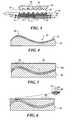
FIGS. 1 and 2 , amold 36, in accordance with the present invention, may be employed insystem 10, and may define a surface having a substantially smooth or planar profile (not shown). Alternatively,mold 36 may include features defined by a plurality of spaced-apart recessions 38 andprotrusions 40. The plurality of features defines an original pattern that is to be transferred into asubstrate 42.Substrate 42 may be comprised of a bare wafer or a wafer with one or more layers disposed thereon. To that end, reduced is a distance “d” betweenmold 36 andsubstrate 42. In this manner, the features onmold 36 may be imprinted into an imprinting material, such aspolymerizable material 24, disposed on a portion ofsurface 44 that presents a substantially planar profile. It should be understood thatsubstrate 42 may be abare silicon wafer 48 or may include a native oxide or one or more layers, shown asprimer layer 45. In the present example,substrate 42 is discussed with respect to including aprimer layer 45. Exemplary compositions from whichprimer layer 45 andpolymerizable material 42 may be formed are discussed in U.S. patent application Ser. No. 11/187,406, filed Jul. 22, 2005, entitled COMPOSITION FOR ADHERING MATERIALS TOGETHER, having Frank Xu listed as the inventor, assigned to the assignee of the present invention and is incorporated by reference herein. - Referring to both
FIGS. 2 and 3 , the imprinting material may be deposited using any known technique, e.g., spin-coating, dip coating and the like. In the present example, however, the imprinting material is deposited as a plurality of spaced-apartdiscrete droplets 46 onsubstrate 42. Imprinting material is formed from a composition that may be selectively polymerized and cross-linked to record the original pattern therein, defining a recorded pattern. - Specifically, the pattern recorded in the imprinting material is produced, in part, by interaction with
mold 36, e.g., electrical interaction, magnetic interaction, thermal interaction, mechanical interaction or the like. In the present example,mold 36 comes into mechanical contact with the imprinting material, spreadingdroplets 46, so as to generate a contiguous layer of the imprinting material oversurface 44 that is solidified into aformation 50.Formation 50 includesprojections 52 and recessedregions 34. A height thickness t1offormation 50 is defined byprojections 52. Recessedregion 54 defines a residual thickness t2offormation 50. In one embodiment, distance “d” is reduced to allow imprinting material to ingress into and fillrecessions 38. To facilitate filling ofrecessions 38, before contact betweenmold 36 anddroplets 46, the atmosphere betweenmold 36 anddroplets 46 is saturated with helium or is completely evacuated or is a partially evacuated atmosphere of helium. - Referring to
FIGS. 2, 3 and4, a problem addressed by the present invention concerns controlling the thickness of t1and t2after reaching a desired distance d. Specifically, exemplary dimensions of the features ofmold 36, e.g., width W1ofprotrusions 40 and width W2ofrecessions 38, may be in the range of 30 to 100 nanometers. Height with thickness t1may be in a range of 400 nanometers to one micrometer ±20-80 nanometers. Residual thickness t2may be in a range of 400 nanometers to one micrometer ±20-80 nanometers. Thus, a height ofprojections 52, measured from anadir surface 55, is in arange 40 to 140 nanometers. As a result,surface 44 presents a non-planar profile, e.g., undulations are present ashills 56 andtroughs 57. The undulations make problematic controlling thicknesses t1and t2. - Referring to
FIGS. 3, 4 and5, undulations make difficult ensuring that thickness t1is substantially equal over the area offormation 150 and thickness t2is substantially equal over the area offormation 150. For example, after solidifying imprinting material,formation 150 is formed in which regions over which thickness t1varies and thickness t2varies. For example, features inregion 58 have a height thickness t′1±δt′1and a residual thickness t′2±δt′2, where δt′1and δt′2results from the variation in thickness t′1and t′2, respectively, due to the curvature ofsurface 44 in superimposition withregion 58. Similarly, features inregion 60 have a height thickness t″1±δt″1and a residual thickness t″2±δt″2, where δt″1and δt″2correspond to the variation in thicknesses t″1and t″2, respectively, due to the curvature ofsurface 44 in superimposition withregion 60. - Referring to
FIGS. 5, 6 and7, were the difference between residual thicknesses t′2±δt′2and t″2±δt″2greater than t′1±δt′1, a distortion in the pattern formed insubstrate 42 would occur. This can be seen afterformation 150 has undergone a break-through etch to exposeregions substrate 42. Were it desired to commence etching ofregions recesses unpatterned region 74 being present that results from no exposure ofsubstrate 42 during the break-through etch. This is undesirable. Were it desired to pattern region84 ofsubstrate 42, etching offormation 150 would occur until a break-through inregion 60 occurs. This would cause substantially all of the features ofregion 58 to be removed. As a result, large regions ofsubstrate 42 would remain unpatterned, due, inter alia, to the absence of masking material. - Referring to
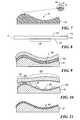
FIGS. 3, 4 and8, to reduce, if not abrogate, the problems presented by the undulations,template 114, including amold 136, is made so as to conform to surface44. In this manner,mold 136 may conform in response to the presence of undulations, thereby minimizing variations among thickness t1and variations among thickness t2over the area offormation 50. To that end,template 114 is fabricated from a relatively thin sheet of fused silica having athickness 113, measured fromopposed sides template 114 to be approximately 4,225 square millimeters. The area ofmold 136 may be any desired, e.g., from 625 square millimeters to be extensive with the area ofsubstrate 42. - Referring to
FIGS. 8-12 the conformableness oftemplate 114 affordsmold 136 the functionality so that control of thicknesses t1and t2may be achieved in the face of undulations. Specifically,mold 136 contacts imprinting material so thatformation 250 may be formed.Formation 250 has afirst surface 252 that rests againstsubstrate 42 and has a profile matching the profile of thesurface 44 ofsubstrate 42 in the presence of undulations. However, a difficulty presented byflexible mold 236 results from the generation of capillary forces betweenmold 136 and the polymerizable material indroplets 46. Upon contact bymold 136 with a first sub-portion of the polymerizable material, e.g.,droplets 46 inregion 158, capillary forces betweenmold 136 and the polymerizable material are generated. However, capillary forces are substantially absent in the remaining sub-section of the polymerizable material, e.g., droplets inregions form formation 250, fluid pressure is applied toside 115 to deformtemplate 114 and, therefore,mold 136 so that thesame contacts droplets 46 inregions - As a result of the flexibility of
mold 136, control of thicknesses t1and t2, is achieved so that thickness t1is within a specified tolerance ±δt1, referred to as being substantially uniform. Similarly thickness t2is substantially uniform in that the same is within a specified tolerance ±δt2. The tolerance results from the distortion in the features that result from themold 136 conforming to surface44. It was determined, however, that by maintaining δt1and δt2to be less than or equal to 5 nanometers over a 25 millimeter area that the distortions that result from the conformableness ofmold 136 are acceptable. Specifically, after a break-through-etch offormation 250,regions 162 over the entire area ofsubstrate 42 are exposed. Thereafter, patterning of the entire surface of substrate may occur, shown asrecessions 164. In this manner, theentire substrate 42 may be patterned, thereby overcoming the problems associated with thickness t1having, as well as thickness t2, varying, over an area ofsubstrate 42 to be patterned. - Referring to both
FIGS. 8 and 13 , althoughtemplate 114 is shown having amold 136 with protrusions lying in a common plane P along withsurface 116, other templates may be employed. For example,template 214 may include amesa 235 that embodiesmold 236. Typically, a height, h, ofmesa 235 is approximately 15 micrometers, as measured fromsurface 216 to a top surface of a protrusion240. - Referring to both
FIGS. 8 and 14 , in another embodiment,template 314 is substantially identical totemplate 114, excepting thatmold 336 is surrounded by anentrainment channel 337.Entrainment channel 337 extends further fromside 316 thanrecessions 338. In yet another embodiment,template 414, shown inFIG. 15 , is substantially identical totemplate 114, shown inFIG. 8 , excepting that regions ofside 416 lying outside ofmold 436 are coplanar withrecessions 438. - Referring to
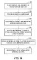
FIGS. 4, 13 and16, during an exemplary operation,template 214 andsubstrate 42 are placed in proximity to one another, e.g., within one millimeter, atstep 500. Atstep 502,template 214 is bowed so thatside 216 facingsubstrate 42 and, therefore,mold 236, both have a convex shape, defining a bowed template. Specifically, a neutral axis, N, ofmold 236 is bowed so that a central portion moves 350-400 micrometers away from neutral axis N so as to have a curved shape. Atstep 504, the relative distance between the bowed template andsubstrate 42 is reduced so that the bowedmold 236 is placed in contact with one or more ofdroplets 46 of imprinting material and subsequently conforms to the shape of the imprinting material disposed betweenmold 236 andsubstrate 42 under compression therebetween. Typically,mold 236 is centered with respect tosubstrate 42 before contacting the imprinting material. Acentral portion 233 ofmold 236 is centered with respect to the area ofsubstrate 42 that is to be patterned. In this example, nearly anentire surface 44 ofsubstrate 44 is to be patterned. The dimension of the area ofsubstrate 42 to be patterned is defined by the thicknesses offormation 250 and the aggregate volume of polymerizable material indroplets 46. As a result, the area ofmold 236 may be greater, less than or equal to the area ofsubstrate 42. Typically,central portion 233 ofmold 236 contacts the center of the area (not shown) with the remaining portions of the imprinting area being subsequently contacted by the non-central portions ofmold 236. - At
step 506, fluid pressure is applied toside 115 to attenuate, if not abrogate, variations among thickness t1of the area offormation 150 and variations among thickness t2over the area offormation 150. Specifically,side 115 is subjected to a sufficient magnitude of fluid pressure to compress imprinting material betweenmold 236 andsubstrate 42 to the state whereby the imprinting material can no longer undergo compression. In this condition, the imprinting material demonstrates visco-elastic properties in that the same behaves as a solid. Further, in the visco-elastic state the imprinting material conforms fully withsurface 44 so that a side of the imprintingmaterial facing mold 236 has the same shape assurface 44.Mold 236 is established to be more compliant than the imprinting material in a visco-elastic state and, therefore, fully conforms to the shape of the side of the imprintingmaterial facing mold 236. Atstep 508, imprinting material is exposed to actinic radiation to solidify the same so as to conform to a shape of themold 236 andsurface 44 ofsubstrate 42. Atstep 510,mold 236 is separated from the solidified imprinting material. - Referring to
FIGS. 12, 17 and18, to facilitate control of the pressures onside 215 oftemplate 214, disposed opposite tomold 236, achuck body 520 is adapted to retaintemplate 214 employing vacuum techniques. To that end,chuck body 520 includes first522 and second524 opposed sides. A side, or edge,surface 526 extends betweenfirst side 520 andsecond side 524.First side 522 includes afirst recess 532 and asecond recess 534, spaced-apart fromfirst recess 532, defining first536 and second538 spaced-apart support regions.First support region 536 cincturessecond support region 538 and the first532 and second534 recesses.Second support region 538 cincturessecond recess 534. Aportion 540 ofchuck body 520 in superimposition withsecond recess 534 is transmissive to energy having a predetermined wavelength, such as the wavelength of actinic energy employed to solidify the polymerizable material mentioned above. To that end,portion 540 is made from a thin layer of material that is transmissive with respect to broad band ultraviolet energy, e.g., glass. However, the material from whichportion 540 is made may depend upon the wavelength of energy produced bysource 26, shown inFIG. 1 . - Referring again to
FIGS. 17 and 18 ,portion 540 extends fromsecond side 524 and terminates proximate tosecond recess 534 and should define an area at least as large as an area ofmold 236 so thatmold 236 is in superimposition therewith. Formed inchuck body 520 are one or more throughways, shown as542 and544. One of the throughways, such asthroughway 542, placesfirst recess 532 in fluid communication withside surface 526. The remaining throughways, such asthroughway 542, placessecond recess 532 in fluid communication withside surface 526. - It should be understood that
throughway 542 may extend betweensecond side 524 andfirst recess 532, as well. Similarly,throughway 544 may extend betweensecond side 524 andsecond recess 534. What is desired is thatthroughways recesses pump system 546. Pump system 546 may include one or more pumps to control the pressure proximate torecesses body 520,template 136 rests against first536 and second538 support regions, covering first532 and second534 recesses.First recess 532 and aportion 548 oftemplate 136 in superimposition therewith define afirst chamber 550.Second recess 534 and a portion552 oftemplate 136 in superimposition therewith define asecond chamber 554.Pump system 546 operates to control a pressure in first550 and second554 chambers. Specifically, the pressure is established infirst chamber 550 to maintain the position of thetemplate 214 with thechuck body 520 and reduce, if not avoid, separation oftemplate 214 fromchuck body 520 under force of gravity {right arrow over (g)}. The pressure insecond chamber 554 may differ from the pressure infirst chamber 548 to reduce, inter alia, distortions in the pattern generated bytemplate 214 during imprinting, by modulating a shape oftemplate 214. For example,pump system 546 may apply a positive pressure inchamber 554 for the reasons discussed above.Pump system 546 is operated under control ofprocessor 32, shown inFIG. 1 .- Referring to
FIGS. 1, 17 and19,template 214 is coupled toimprint head 20 via coupling ofchuck body 520 to aflexure 556 that is coupled to anorientation system 558.Orientation system 558 movestemplate 214.Flexure 556 is disclosed and claimed in U.S. patent application Ser. No. 11/142,838, filed Jun. 1, 2005, entitled “Compliant Device for Nano-Scale Manufacturing”, which is assigned to the assignee of the present invention, and is incorporated by reference herein.Orientation system 558 is disclosed in U.S. patent application Ser. No. 11/142,825, filed Jun. 1, 2005 entitled “Method and System to Control Movement of a Body for Nano-Scale Manufacturing,” which is assigned to the assignee of the present invention and incorporated by reference herein. - Referring to both
FIGS. 19 and 20 ,orientation system 558 is shown having aninner frame 560 disposed proximate to anouter frame 562, andflexure ring 564, discussed more fully below.Body 520 is coupled toorientation system 558 throughflexure 556. Specifically,body 520 is connected to flexure556, using any suitable means, such as threaded fasteners (not shown) located at the four corners ofbody 520 connecting to four corners offlexure 556 closest to the four corners ofbody 520. Four corners566 offlexure 556 that are closest to asurface 568 ofinner frame 560 are connected thereto using any suitable means, such as threaded fasteners, not shown. Inner frame 560 has acentral throughway 570, andouter frame 562 has acentral opening 572 in superimposition withcentral throughway 570.Flexure ring 564 has an annular shape, e.g., circular or elliptical, and is coupled toinner frame 560 andouter frame 562 and lies outside of bothcentral throughway 570 andcentral opening 572. Specifically,flexure ring 564 is coupled toinner frame 560 atregions outer frame 562 atregions Region 580 is disposed betweenregions region 582 is disposed betweenregions regions flexure ring 564 surroundsflexure 556,body 520, andtemplate 214 and fixedly attachesinner frame 560 toouter frame 562.- It should be understood that the components of
orientation system 558 andflexure 556 may be formed from any suitable material, e.g., aluminum, stainless steel and the like. Additionally,flexure 556 may be coupled toorientation system 558 using any suitable means. In the present example,flexure 556 is coupled to surface45 employing threaded fasteners (not shown) located at the fourcorners 586. - Referring to
FIGS. 17 and 19 ,system 558 is configured to control movement oftemplate 214 and to place the same in a desired spatial relationship with respect to a reference surface, such assubstrate 42 disposed onstage 11. To that end, a plurality ofactuators outer frame 562 andinner frame 560 so as to be spaced aboutorientation system 558. Each ofactuators second end 596. First end594 facesouter frame 562, andsecond end 596 faces away fromouter frame 562. - Referring to both
FIGS. 19 and 20 ,actuators inner frame 560 with respect toouter frame 562 by facilitating translational motion ofinner frame 560 along three axes Z1, Z2, and Z3.Orientation system 558 may provide a range of motion of approximately ±1.2 mm about axes Z1, Z2, and Z3. In this fashion,actuators inner frame 560 to impart angular motion to bothflexure 556 and, therefore,template 214 andbody 520, about one or more of a plurality of axes T1, T2and T3. Specifically, by decreasing a distance betweeninner frame 560 andouter frame 562 along axes Z2and Z3and increasing a distance therebetween along axis Z1, angular motion about tilt axis T2occurs in a first direction. - Increasing the distance between
inner frame 560 andouter frame 562 along axes Z2and Z3and decreasing the distance therebetween along axis Z1, angular motion about tilt axis T2occurs in a second direction opposite to the first direction. In a similar manner angular movement about axis T1may occur by varying the distance betweeninner frame 560 andouter frame 562 by movement ofinner frame 560 along axes Z1and Z2in the same direction and magnitude while moving of theinner frame 560 along axis Z3in a direction opposite and twice to the movement along axes Z1and Z2. Similarly, angular movement about axis T3may occur by varying the distance betweeninner frame 560 andouter frame 562 by movement ofinner frame 560 along axes Z1and Z3in the same direction and magnitude while moving ofinner frame 560 along axis Z2in direction opposite and twice to the movement along axes Z1and Z3.Actuators N. Orientation System 558 may provide a range of motion of approximately ±0.15° about axes T1, T2, and T3. Actuators actuators actuators inner frame 560 using any suitable means, e.g., threaded fasteners. Additionally,actuators inner frame 560 andouter frame 562 so as to be symmetrically disposed thereabout and lie outside ofcentral throughway 570 andcentral opening 572. With this configuration an unobstructed throughway betweenouter frame 562 toflexure 556 is configured. Additionally, the symmetrical arrangement minimizes dynamic vibration and uneven thermal drift, thereby providing fine-motion correction ofinner frame 560.- The combination of the
inner frame 560,outer frame 562,flexure ring 564 andactuators flexure 556 and, therefore,body 520 andtemplate 214 about tilt axes T1, T2and T3. It is desired, however, that translational motion be imparted totemplate 214 along axes that lie in a plane extending transversely, if not orthogonally, to axes Z1, Z2, and Z3. This is achieved by providingflexure 556 with the functionality to impart angular motion upontemplate 214 about one or more of a plurality of compliance axes, shown as C1 and C2, which are spaced—part from tilt axes T1, T2and T3and exist on the surface of the template when the template, the template chuck, and the compliant device are assembled. - Another embodiment of the present invention facilitates separation of
mold 236 from the solidified imprinting material which forms, for example,formation 50. This is based upon the finding that localizing initial separation to a relatively small area of the interface betweenmold 236 and the solidified imprinting material reduces the magnitude of upwardly forces imparted uponmold 236 byorientation system 558 necessary to achieve separation. A desirable result is that the probability of separation betweensubstrate 42 andstage 11 is reduced. - Referring to
FIG. 21 , a deleterious situation that the present invention seeks to avoid separation ofsubstrate 42 fromstage 11 upon separation ofmold 236 fromformation 50.Imprint head 20 applies a sufficient force to overcome the forces of attraction betweenmold 236 andformation 50. In the situation in which the area ofmold 236 is substantially co-extensive with the area ofsubstrate 42, e.g., whole wafer imprinting, the force required to separatemold 236 fromformation 50 is often much greater than the force of attraction betweensubstrate 42 andstage 11, e.g., a vacuum or electrostatic force of attraction betweensubstrate 42 andstage 11. Therefore, it is desirable to reduce the force applied totemplate 214 necessary to achieve separation ofmold 236 fromformation 50. Specifically, it is desirable to ensure that the upwardly force required to separatetemplate 114 fromformation 50 is less than the downwardly applied bystage 11 tosubstrate 42 to maintain the same thereupon. - The upwardly force required to separate
template 214 fromformation 50 is reduced by creating localized separation betweenmold 236 andformation 50 at a region proximate to a periphery ofmold 236. To that end, formold 236 having an area substantially coextensive withsubstrate 42,mold 236 will have a maximum area to ensure that aperimeter 237 thereof is spaced-apart from anedge 222 ofsubstrate 42 approximately 1 millimeter, shown as distance R. Localized separation is obtained by initiating separation ofmold 236 from the solidified imprinting material employingpump system 546pressurizing chamber 554 to approximately 20 kPa. This distorts the shape of aregion 217 oftemplate 214 that surroundsmold 236. Afirst portion 219 of thesurface template 214 inregion 217 is displaced downwardly away from a neutral position NPtowardsubstrate 42, with the nadir ofportion 219 being approximately 1 micrometer belowsurface 43 ofsubstrate 42. As a result, the distortion afforded totemplate 214 bypump system 546 should be sufficient to allownadir portion 219 to extend from the neutral position NPa magnitude that is greater than the thickness t1, shown inFIG. 3 , and height h, shown inFIG. 13 . - Referring again to
FIGS. 21 and 22 , asecond portion 220 of the surface oftemplate 214 moves upwardly away fromsubstrate 42, with an apex thereof being spaced-apart fromsurface 43 approximately fifteen micrometers. A segment of template disposed betweensecond portion 220 andnadir portion 219 contacts edge222 ofsubstrate 42. The Young's modulus associated withtemplate 214 results in a returning force FRto facilitate returningregion 217 to neutral position NP, wherein undulations shown asnadir portion 219 and second portion are attenuated to formarcuate surface 224. The returning force FRresults from the material oftemplate 214 undergoing movement to return to a reduced-stressed and/or reduced-strained state. - Referring to both
FIGS. 21, 24 and25, the returning force FRcauses anarea 221 ofmold 236 proximate toregion 217 to separate fromsubstrate 42, whilesegment 227 functions to presssubstrate 42 downwardly againststage 11, firmly securing the same together. In this manner,separation mold 236 fromformation 50 occurs by cantileveringtemplate 214 with respect tosubstrate 42. Specifically,portion 227 contacts edge222 ofsubstrate 42 holding the same againststage 11, which reduces the upwardly force ontemplate 214 required to separatemold 236 from substrate and preventssubstrate 42 from separating fromstage 11. It can be said, therefore, that returning force FRreduces the magnitude of the upwardly forces imparted uponmold 236 byorientation system 558 that are necessary to achieve separation. As a result, returning force FRmust be greater than the adhering force betweenarea 221 andformation 50. The returning force FRresults in an oblique angle θ being formed with respect toformation 50, measured for example, between a plane P2in which nadir surfaces138 ofrecessions 38 lie and a plane P3in which nadir surfaces154 of recessedregions 54 lie. The back pressure and returning force FRcoupled with the angle θ, causestemplate 214 and, therefore,mold 236, to have an arcuate shape in whichregion 221 is further fromformation 50 than regions ofmold 236 disposed remotely therefrom, center portions ofmold 236 located proximate to center axis A. Typically, the angle θ will be on the order of micro-radians so that shearing of features in solidifiedlayer 50 is on the order of pico-meters. The remaining portions ofmold 236 are separated fromformation 50 may be controlled by operation ofactuators FIG. 19 . - Referring to both
FIGS. 19 and 25 , by havingactuators mold 236 is separated from formation so that the last portions thereof proximate toregion 221 are separated fromformation 50 before regions proximate to center axis A. In this manner, regions ofmold 236 that are radially symmetrically disposed about axis A are sequentially separated fromformation 50, e.g.,region 221 separates thenregion 223, thenregion 225 and etc. It should be understood, however, thatregions mold 236. It is entirely possible thatmold 236 have a rectangular or square shape. As a result, the shape of regions sequentially removed fromformation 50 would be complementary to the shape ofperimeter 237. As a result, regions ofmold 236 that are concentric with respect toperimeter 237 are sequentially separated fromformation 50. It should be understood, however, thatactuators mold 236 fromformation 50. This may be achieved by movingmold 236 about on of tilt axes T1, T2and T3. - Referring to
FIGS. 21 and 22 , another manner to achieve localized separation oftemplate 214 would include formingarcuate surface 224 of template that is proximate tomold 236. Specifically,pump system 546 would create a pressure in pressurizingchamber 554 sufficient to bowarcuate surface 224 and provide the same with a substantially constant radius of curvature. The returning force FRwould induce localized separation betweenmold 236 andformation 50 proximate toregion 221, as discussed above. Thereafter,mold 236 may be separated fromformation 50 employing the techniques discussed above. Forming contoured surface is particularly advantageous weremold 236 sized so as to be much smaller than the area ofsubstrate 42, e.g., weremold 236 to have an area of 625 square millimeters, cantilevering would not occur. - The embodiments of the present invention described above are exemplary. Many changes and modifications may be made to the disclosure recited above, while remaining within the scope of the invention. The scope of the invention should not, therefore, be limited by the above description, but instead should be determined with reference to the appended claims along with their full scope of equivalents.
Claims (21)
Priority Applications (9)
| Application Number | Priority Date | Filing Date | Title |
|---|---|---|---|
| US11/303,777US7906058B2 (en) | 2005-12-01 | 2005-12-16 | Bifurcated contact printing technique |
| EP06804074AEP1954472A4 (en) | 2005-12-01 | 2006-09-22 | Technique for separating a mold from solidified imprinting material |
| KR1020087012782AKR101340922B1 (en) | 2005-12-01 | 2006-09-22 | Technique for separating a mold from solidified imprinting material |
| EP11186734AEP2413189A1 (en) | 2005-12-01 | 2006-09-22 | A method for spreading a conformable material between a substrate and a template |
| KR1020137014437AKR101375132B1 (en) | 2005-12-01 | 2006-09-22 | Technique for separating a mold from solidified imprinting material |
| PCT/US2006/037109WO2007064386A1 (en) | 2005-12-01 | 2006-09-22 | Technique for separating a mold from solidified imprinting material |
| JP2008543272AJP5236484B2 (en) | 2005-12-01 | 2006-09-22 | Method for separating a mold from a solidified imprinting material |
| TW095137688ATWI310730B (en) | 2005-12-01 | 2006-10-13 | Technique for separating a mold from solidified imprinting material |
| JP2012016219AJP5543502B2 (en) | 2005-12-01 | 2012-01-30 | Method for separating a mold from a solidified imprinting material |
Applications Claiming Priority (2)
| Application Number | Priority Date | Filing Date | Title |
|---|---|---|---|
| US11/292,568US7803308B2 (en) | 2005-12-01 | 2005-12-01 | Technique for separating a mold from solidified imprinting material |
| US11/303,777US7906058B2 (en) | 2005-12-01 | 2005-12-16 | Bifurcated contact printing technique |
Related Parent Applications (1)
| Application Number | Title | Priority Date | Filing Date |
|---|---|---|---|
| US11/292,568DivisionUS7803308B2 (en) | 2005-12-01 | 2005-12-01 | Technique for separating a mold from solidified imprinting material |
Publications (2)
| Publication Number | Publication Date |
|---|---|
| US20070126150A1true US20070126150A1 (en) | 2007-06-07 |
| US7906058B2 US7906058B2 (en) | 2011-03-15 |
Family
ID=38092554
Family Applications (1)
| Application Number | Title | Priority Date | Filing Date |
|---|---|---|---|
| US11/303,777Active2027-10-23US7906058B2 (en) | 2005-12-01 | 2005-12-16 | Bifurcated contact printing technique |
Country Status (6)
| Country | Link |
|---|---|
| US (1) | US7906058B2 (en) |
| EP (2) | EP1954472A4 (en) |
| JP (2) | JP5236484B2 (en) |
| KR (2) | KR101375132B1 (en) |
| TW (1) | TWI310730B (en) |
| WO (1) | WO2007064386A1 (en) |
Cited By (33)
| Publication number | Priority date | Publication date | Assignee | Title |
|---|---|---|---|---|
| US20070228609A1 (en)* | 2006-04-03 | 2007-10-04 | Molecular Imprints, Inc. | Imprinting of Partial Fields at the Edge of the Wafer |
| US20070228610A1 (en)* | 2006-04-03 | 2007-10-04 | Molecular Imprints, Inc. | Method of Concurrently Patterning a Substrate Having a Plurality of Fields and a Plurality of Alignment Marks |
| US20070231981A1 (en)* | 2006-04-03 | 2007-10-04 | Molecular Imprints, Inc. | Patterning a Plurality of Fields on a Substrate to Compensate for Differing Evaporation Times |
| US20080145774A1 (en)* | 2006-10-06 | 2008-06-19 | Asml Netherlands B.V. | Imprint lithography |
| US20080174046A1 (en)* | 2002-07-11 | 2008-07-24 | Molecular Imprints Inc. | Capillary Imprinting Technique |
| US20080303187A1 (en)* | 2006-12-29 | 2008-12-11 | Molecular Imprints, Inc. | Imprint Fluid Control |
| US20090014917A1 (en)* | 2007-07-10 | 2009-01-15 | Molecular Imprints, Inc. | Drop Pattern Generation for Imprint Lithography |
| US20090108484A1 (en)* | 2007-10-11 | 2009-04-30 | Asml Netherlands B.V. | Imprint lithography |
| US20090115110A1 (en)* | 2007-11-02 | 2009-05-07 | Molecular Imprints, Inc. | Drop Pattern Generation for Imprint Lithography |
| US20090148619A1 (en)* | 2007-12-05 | 2009-06-11 | Molecular Imprints, Inc. | Controlling Thickness of Residual Layer |
| US7547398B2 (en) | 2006-04-18 | 2009-06-16 | Molecular Imprints, Inc. | Self-aligned process for fabricating imprint templates containing variously etched features |
| US20090200710A1 (en)* | 2008-02-08 | 2009-08-13 | Molecular Imprints, Inc. | Extrusion reduction in imprint lithography |
| US7670529B2 (en) | 2005-12-08 | 2010-03-02 | Molecular Imprints, Inc. | Method and system for double-sided patterning of substrates |
| US7670530B2 (en) | 2006-01-20 | 2010-03-02 | Molecular Imprints, Inc. | Patterning substrates employing multiple chucks |
| US7691313B2 (en) | 2002-11-13 | 2010-04-06 | Molecular Imprints, Inc. | Method for expelling gas positioned between a substrate and a mold |
| US20100098859A1 (en)* | 2008-10-21 | 2010-04-22 | Molecular Imprints, Inc. | Drop Pattern Generation with Edge Weighting |
| US20100096775A1 (en)* | 2008-10-16 | 2010-04-22 | Koh Teng Hwee | Mold imprinting |
| US20100096764A1 (en)* | 2008-10-20 | 2010-04-22 | Molecular Imprints, Inc. | Gas Environment for Imprint Lithography |
| US20100112220A1 (en)* | 2008-11-03 | 2010-05-06 | Molecular Imprints, Inc. | Dispense system set-up and characterization |
| US7727453B2 (en) | 2002-07-11 | 2010-06-01 | Molecular Imprints, Inc. | Step and repeat imprint lithography processes |
| US7803308B2 (en) | 2005-12-01 | 2010-09-28 | Molecular Imprints, Inc. | Technique for separating a mold from solidified imprinting material |
| US20100289182A1 (en)* | 2007-09-28 | 2010-11-18 | Yuma Hirai | method and device for manufacturing sheet having fine shape transferred thereon |
| US7981481B2 (en) | 2004-09-23 | 2011-07-19 | Molecular Imprints, Inc. | Method for controlling distribution of fluid components on a body |
| US8012395B2 (en) | 2006-04-18 | 2011-09-06 | Molecular Imprints, Inc. | Template having alignment marks formed of contrast material |
| US20120126447A1 (en)* | 2010-11-18 | 2012-05-24 | Fuh-Yu Chang | Micro/nano imprint mold of the fabricating process and the method of fabricating high aspect ratio anti-etch structure by utilizing thereof |
| US8211214B2 (en) | 2003-10-02 | 2012-07-03 | Molecular Imprints, Inc. | Single phase fluid imprint lithography method |
| US8215946B2 (en) | 2006-05-18 | 2012-07-10 | Molecular Imprints, Inc. | Imprint lithography system and method |
| US8586126B2 (en) | 2008-10-21 | 2013-11-19 | Molecular Imprints, Inc. | Robust optimization to generate drop patterns in imprint lithography which are tolerant of variations in drop volume and drop placement |
| US9272462B2 (en) | 2010-03-29 | 2016-03-01 | Fujifilm Corporation | Minute convexo-concave pattern forming method and forming device, and transfer substrate producing method and transfer substrate |
| US20160091788A1 (en)* | 2013-04-22 | 2016-03-31 | Dai Nippon Printing Co., Ltd. | Imprint mold and method for designing dummy pattern |
| US20170062227A1 (en)* | 2015-08-26 | 2017-03-02 | Tokyo Electron Limited | Seasoning method and etching method |
| US20180056577A1 (en)* | 2016-08-25 | 2018-03-01 | National Cheng Kung University | Flexible mold with variable thickness |
| EP4070160A1 (en)* | 2019-12-02 | 2022-10-12 | EV Group E. Thallner GmbH | Method and apparatus for removal of a stamp |
Families Citing this family (17)
| Publication number | Priority date | Publication date | Assignee | Title |
|---|---|---|---|---|
| US7162035B1 (en) | 2000-05-24 | 2007-01-09 | Tracer Detection Technology Corp. | Authentication method and system |
| US7995196B1 (en) | 2008-04-23 | 2011-08-09 | Tracer Detection Technology Corp. | Authentication method and system |
| CN102349131A (en) | 2009-03-12 | 2012-02-08 | 应用材料公司 | Large area dissolvable template lithography |
| JP5662741B2 (en)* | 2009-09-30 | 2015-02-04 | キヤノン株式会社 | Imprint apparatus and article manufacturing method |
| JP5491931B2 (en)* | 2010-03-30 | 2014-05-14 | 富士フイルム株式会社 | Nanoimprint method and mold manufacturing method |
| EP2564271B1 (en) | 2010-04-27 | 2015-12-16 | Canon Nanotechnologies, Inc. | Separation control substrate/template for nanoimprint lithography |
| JP5646396B2 (en)* | 2011-06-08 | 2014-12-24 | 株式会社東芝 | Template manufacturing method |
| JP5938218B2 (en) | 2012-01-16 | 2016-06-22 | キヤノン株式会社 | Imprint apparatus, article manufacturing method, and imprint method |
| JP5824380B2 (en)* | 2012-02-07 | 2015-11-25 | キヤノン株式会社 | Imprint apparatus, imprint method, and article manufacturing method |
| JP5824379B2 (en)* | 2012-02-07 | 2015-11-25 | キヤノン株式会社 | Imprint apparatus, imprint method, and article manufacturing method |
| KR102336499B1 (en)* | 2014-08-04 | 2021-12-07 | 삼성전자주식회사 | Pattern structure and method of manufacturing the pattern structure, and liquid crystal display device having metal wire grid polarizer |
| EP3237971B1 (en)* | 2014-12-22 | 2021-11-17 | Koninklijke Philips N.V. | Patterned stamp manufacturing method, patterned stamp and imprinting method |
| WO2017066546A1 (en)* | 2015-10-15 | 2017-04-20 | Board Of Regents, The University Of Texas System | Versatile process for precision nanoscale manufacturing |
| US9993962B2 (en)* | 2016-05-23 | 2018-06-12 | Canon Kabushiki Kaisha | Method of imprinting to correct for a distortion within an imprint system |
| US10627715B2 (en) | 2016-10-31 | 2020-04-21 | Canon Kabushiki Kaisha | Method for separating a nanoimprint template from a substrate |
| US11249405B2 (en)* | 2018-04-30 | 2022-02-15 | Canon Kabushiki Kaisha | System and method for improving the performance of a nanoimprint system |
| JP7507641B2 (en) | 2020-09-08 | 2024-06-28 | キヤノン株式会社 | Molding apparatus and method for manufacturing an article |
Citations (94)
| Publication number | Priority date | Publication date | Assignee | Title |
|---|---|---|---|---|
| US2124711A (en)* | 1937-06-25 | 1938-07-26 | George S Rowell | Method and apparatus for reproducing images on curved surfaces |
| US4022855A (en)* | 1975-03-17 | 1977-05-10 | Eastman Kodak Company | Method for making a plastic optical element having a gradient index of refraction |
| US4070116A (en)* | 1975-06-23 | 1978-01-24 | International Business Machines Corporation | Gap measuring device for defining the distance between two or more surfaces |
| US4208240A (en)* | 1979-01-26 | 1980-06-17 | Gould Inc. | Method and apparatus for controlling plasma etching |
| US4440804A (en)* | 1982-08-02 | 1984-04-03 | Fairchild Camera & Instrument Corporation | Lift-off process for fabricating self-aligned contacts |
| US4521445A (en)* | 1982-09-07 | 1985-06-04 | Energy Sciences, Inc. | Method and apparatus for electron curing on a cooled drum |
| US4576900A (en)* | 1981-10-09 | 1986-03-18 | Amdahl Corporation | Integrated circuit multilevel interconnect system and method |
| US4637904A (en)* | 1983-11-14 | 1987-01-20 | Rohm And Haas Company | Process for molding a polymeric layer onto a substrate |
| US4676868A (en)* | 1986-04-23 | 1987-06-30 | Fairchild Semiconductor Corporation | Method for planarizing semiconductor substrates |
| US4737425A (en)* | 1986-06-10 | 1988-04-12 | International Business Machines Corporation | Patterned resist and process |
| US4908298A (en)* | 1985-03-19 | 1990-03-13 | International Business Machines Corporation | Method of creating patterned multilayer films for use in production of semiconductor circuits and systems |
| US4909151A (en)* | 1986-11-10 | 1990-03-20 | Matsushita Electric Industrial Co., Ltd. | Method of forming an ink image and printing the formed image |
| US4919748A (en)* | 1989-06-30 | 1990-04-24 | At&T Bell Laboratories | Method for tapered etching |
| US4921778A (en)* | 1988-07-29 | 1990-05-01 | Shipley Company Inc. | Photoresist pattern fabrication employing chemically amplified metalized material |
| US5003062A (en)* | 1990-04-19 | 1991-03-26 | Taiwan Semiconductor Manufacturing Co. | Semiconductor planarization process for submicron devices |
| US5028361A (en)* | 1987-11-09 | 1991-07-02 | Takeo Fujimoto | Method for molding a photosensitive composition |
| US5110514A (en)* | 1989-05-01 | 1992-05-05 | Soane Technologies, Inc. | Controlled casting of a shrinkable material |
| US5124089A (en)* | 1986-12-25 | 1992-06-23 | Sony Corporation | Method of producing transmissive screens |
| US5126006A (en)* | 1990-10-30 | 1992-06-30 | International Business Machines Corp. | Plural level chip masking |
| US5212147A (en)* | 1991-05-15 | 1993-05-18 | Hewlett-Packard Company | Method of forming a patterned in-situ high Tc superconductive film |
| US5277749A (en)* | 1991-10-17 | 1994-01-11 | International Business Machines Corporation | Methods and apparatus for relieving stress and resisting stencil delamination when performing lift-off processes that utilize high stress metals and/or multiple evaporation steps |
| US5288436A (en)* | 1990-11-06 | 1994-02-22 | Colloptics, Inc. | Methods of fabricating a collagen lenticule precursor for modifying the cornea |
| US5324683A (en)* | 1993-06-02 | 1994-06-28 | Motorola, Inc. | Method of forming a semiconductor structure having an air region |
| US5328810A (en)* | 1990-05-07 | 1994-07-12 | Micron Technology, Inc. | Method for reducing, by a factor or 2-N, the minimum masking pitch of a photolithographic process |
| US5330881A (en)* | 1989-06-02 | 1994-07-19 | Digital Equipment Corp. | Microlithographic method for producing thick, vertically-walled photoresist patterns |
| US5422295A (en)* | 1992-12-10 | 1995-06-06 | Samsung Electronics Co., Ltd. | Method for forming a semiconductor memory device having a vertical multi-layered storage electrode |
| US5424549A (en)* | 1991-12-20 | 1995-06-13 | Board Of Supervisors Of Louisiana State University And Agricultural And Mechanical College | Scanning systems for high resolution e-beam and X-ray lithography |
| US5425848A (en)* | 1993-03-16 | 1995-06-20 | U.S. Philips Corporation | Method of providing a patterned relief of cured photoresist on a flat substrate surface and device for carrying out such a method |
| US5431777A (en)* | 1992-09-17 | 1995-07-11 | International Business Machines Corporation | Methods and compositions for the selective etching of silicon |
| US5434107A (en)* | 1994-01-28 | 1995-07-18 | Texas Instruments Incorporated | Method for planarization |
| US5480047A (en)* | 1993-06-04 | 1996-01-02 | Sharp Kabushiki Kaisha | Method for forming a fine resist pattern |
| US5628917A (en)* | 1995-02-03 | 1997-05-13 | Cornell Research Foundation, Inc. | Masking process for fabricating ultra-high aspect ratio, wafer-free micro-opto-electromechanical structures |
| US5643364A (en)* | 1994-11-30 | 1997-07-01 | Applied Materials, Inc. | Plasma chamber with fixed RF matching |
| US5736424A (en)* | 1987-02-27 | 1998-04-07 | Lucent Technologies Inc. | Device fabrication involving planarization |
| US5753014A (en)* | 1993-11-12 | 1998-05-19 | Van Rijn; Cornelis Johannes Maria | Membrane filter and a method of manufacturing the same as well as a membrane |
| US5772905A (en)* | 1995-11-15 | 1998-06-30 | Regents Of The University Of Minnesota | Nanoimprint lithography |
| US5871558A (en)* | 1994-08-04 | 1999-02-16 | Hitachi Chemical Company, Ltd. | Process for producing silica glass |
| US5888650A (en)* | 1996-06-03 | 1999-03-30 | Minnesota Mining And Manufacturing Company | Temperature-responsive adhesive article |
| US5895263A (en)* | 1996-12-19 | 1999-04-20 | International Business Machines Corporation | Process for manufacture of integrated circuit device |
| US5900160A (en)* | 1993-10-04 | 1999-05-04 | President And Fellows Of Harvard College | Methods of etching articles via microcontact printing |
| US5907782A (en)* | 1998-08-15 | 1999-05-25 | Acer Semiconductor Manufacturing Inc. | Method of forming a multiple fin-pillar capacitor for a high density dram cell |
| US5926690A (en)* | 1997-05-28 | 1999-07-20 | Advanced Micro Devices, Inc. | Run-to-run control process for controlling critical dimensions |
| US6046056A (en)* | 1996-06-28 | 2000-04-04 | Caliper Technologies Corporation | High throughput screening assay systems in microscale fluidic devices |
| US6048799A (en)* | 1987-02-27 | 2000-04-11 | Lucent Technologies Inc. | Device fabrication involving surface planarization |
| US6067144A (en)* | 1996-10-23 | 2000-05-23 | Kabushiki Kaisha Toshiba | LCD cell having two supporting gap members different in height |
| US6074827A (en)* | 1996-07-30 | 2000-06-13 | Aclara Biosciences, Inc. | Microfluidic method for nucleic acid purification and processing |
| US6180239B1 (en)* | 1993-10-04 | 2001-01-30 | President And Fellows Of Harvard College | Microcontact printing on surfaces and derivative articles |
| US6218316B1 (en)* | 1998-10-22 | 2001-04-17 | Micron Technology, Inc. | Planarization of non-planar surfaces in device fabrication |
| US6242363B1 (en)* | 1999-08-11 | 2001-06-05 | Adc Telecommunications, Inc. | Method of etching a wafer layer using a sacrificial wall to form vertical sidewall |
| US6245213B1 (en)* | 1996-09-06 | 2001-06-12 | Obducat Ab | Method for anisotropic etching of structures in conducting materials |
| US6334960B1 (en)* | 1999-03-11 | 2002-01-01 | Board Of Regents, The University Of Texas System | Step and flash imprint lithography |
| US6337262B1 (en)* | 2000-03-06 | 2002-01-08 | Chartered Semiconductor Manufacturing Ltd. | Self aligned T-top gate process integration |
| US6376379B1 (en)* | 2000-02-01 | 2002-04-23 | Chartered Semiconductor Manufacturing Ltd. | Method of hard mask patterning |
| US6383928B1 (en)* | 1999-09-02 | 2002-05-07 | Texas Instruments Incorporated | Post copper CMP clean |
| US6387783B1 (en)* | 1999-04-26 | 2002-05-14 | International Business Machines Corporation | Methods of T-gate fabrication using a hybrid resist |
| US6388253B1 (en)* | 1999-06-29 | 2002-05-14 | Applied Materials, Inc. | Integrated critical dimension control for semiconductor device manufacturing |
| US6391798B1 (en)* | 1987-02-27 | 2002-05-21 | Agere Systems Guardian Corp. | Process for planarization a semiconductor substrate |
| US20020094496A1 (en)* | 2000-07-17 | 2002-07-18 | Choi Byung J. | Method and system of automatic fluid dispensing for imprint lithography processes |
| US6423207B1 (en)* | 1998-03-05 | 2002-07-23 | Obducat Ab | Method and apparatus for etching |
| US6503829B2 (en)* | 2000-08-19 | 2003-01-07 | Samsung Electronics Co., Ltd. | Metal via contact of a semiconductor device and method for fabricating the same |
| US20030017424A1 (en)* | 2001-07-18 | 2003-01-23 | Miri Park | Method and apparatus for fabricating complex grating structures |
| US6514672B2 (en)* | 1999-06-17 | 2003-02-04 | Taiwan Semiconductor Manufacturing Company | Dry development process for a bi-layer resist system |
| US6517977B2 (en)* | 2001-03-28 | 2003-02-11 | Motorola, Inc. | Lithographic template and method of formation and use |
| US6517995B1 (en)* | 1999-09-14 | 2003-02-11 | Massachusetts Institute Of Technology | Fabrication of finely featured devices by liquid embossing |
| US6521536B1 (en)* | 1999-01-11 | 2003-02-18 | Micron Technology, Inc. | Planarization process |
| US6534418B1 (en)* | 2001-04-30 | 2003-03-18 | Advanced Micro Devices, Inc. | Use of silicon containing imaging layer to define sub-resolution gate structures |
| US6541360B1 (en)* | 2001-04-30 | 2003-04-01 | Advanced Micro Devices, Inc. | Bi-layer trim etch process to form integrated circuit gate structures |
| US20030092261A1 (en)* | 2000-12-04 | 2003-05-15 | Fumio Kondo | Substrate processing method |
| US6565928B2 (en)* | 1999-03-08 | 2003-05-20 | Tokyo Electron Limited | Film forming method and film forming apparatus |
| US20030129542A1 (en)* | 2001-10-31 | 2003-07-10 | Brewer Science, Inc. | Contact planarization materials that generate no volatile byproducts or residue during curing |
| US20040029041A1 (en)* | 2002-02-27 | 2004-02-12 | Brewer Science, Inc. | Novel planarization method for multi-layer lithography processing |
| US6696220B2 (en)* | 2000-10-12 | 2004-02-24 | Board Of Regents, The University Of Texas System | Template for room temperature, low pressure micro-and nano-imprint lithography |
| US20040038552A1 (en)* | 2002-08-23 | 2004-02-26 | Watts Michael P.C. | Method for fabricating bulbous-shaped vias |
| US20040036201A1 (en)* | 2000-07-18 | 2004-02-26 | Princeton University | Methods and apparatus of field-induced pressure imprint lithography |
| US20040046288A1 (en)* | 2000-07-18 | 2004-03-11 | Chou Stephen Y. | Laset assisted direct imprint lithography |
| US20040065976A1 (en)* | 2002-10-04 | 2004-04-08 | Sreenivasan Sidlgata V. | Method and a mold to arrange features on a substrate to replicate features having minimal dimensional variability |
| US20040065252A1 (en)* | 2002-10-04 | 2004-04-08 | Sreenivasan Sidlgata V. | Method of forming a layer on a substrate to facilitate fabrication of metrology standards |
| US6842229B2 (en)* | 2000-07-16 | 2005-01-11 | Board Of Regents, The University Of Texas System | Imprint lithography template comprising alignment marks |
| US20050056963A1 (en)* | 2003-07-10 | 2005-03-17 | Mccutcheon Jeremy W. | Automated process and apparatus for planarization of topographical surfaces |
| US6870301B2 (en)* | 1999-10-29 | 2005-03-22 | Board Of Regents, The University Of Texas System | Method of separating a template from a substrate during imprint lithography |
| US20050061773A1 (en)* | 2003-08-21 | 2005-03-24 | Byung-Jin Choi | Capillary imprinting technique |
| US20050072757A1 (en)* | 2003-10-02 | 2005-04-07 | University Of Texas System Board Of Regents | Method of creating a turbulent flow of fluid between a mold and a substrate |
| US20050106321A1 (en)* | 2003-11-14 | 2005-05-19 | Molecular Imprints, Inc. | Dispense geometery to achieve high-speed filling and throughput |
| US20060017876A1 (en)* | 2004-07-23 | 2006-01-26 | Molecular Imprints, Inc. | Displays and method for fabricating displays |
| US6990870B2 (en)* | 2002-12-12 | 2006-01-31 | Molecular Imprints, Inc. | System for determining characteristics of substrates employing fluid geometries |
| US20060062867A1 (en)* | 2002-07-11 | 2006-03-23 | Molecular Imprints, Inc. | Formation of discontinuous films during an imprint lithography process |
| US20060063112A1 (en)* | 2004-09-21 | 2006-03-23 | Molecular Imprints, Inc. | Pattern reversal employing thick residual layers |
| US7019819B2 (en)* | 2002-11-13 | 2006-03-28 | Molecular Imprints, Inc. | Chucking system for modulating shapes of substrates |
| US20060068120A1 (en)* | 2004-09-27 | 2006-03-30 | Molecular Imprints, Inc. | Method of compensating for a volumetric shrinkage of a material disposed upon a substrate to form a substantially planar structure therefrom |
| US20060076717A1 (en)* | 2002-07-11 | 2006-04-13 | Molecular Imprints, Inc. | Step and repeat imprint lithography processes |
| US20060113697A1 (en)* | 2004-12-01 | 2006-06-01 | Molecular Imprints, Inc. | Eliminating printability of sub-resolution defects in imprint lithography |
| US20060115999A1 (en)* | 2004-12-01 | 2006-06-01 | Molecular Imprints, Inc. | Methods of exposure for the purpose of thermal management for imprint lithography processes |
| US20060121728A1 (en)* | 2004-12-07 | 2006-06-08 | Molecular Imprints, Inc. | Method for fast filling of templates for imprint lithography using on template dispense |
| US20070063384A1 (en)* | 2005-09-21 | 2007-03-22 | Molecular Imprints, Inc. | Method to control an atmostphere between a body and a substrate |
Family Cites Families (159)
| Publication number | Priority date | Publication date | Assignee | Title |
|---|---|---|---|---|
| US1236304A (en)* | 1917-02-03 | 1917-08-07 | Riley L Howell | Cushioned hand-stamp. |
| US2201302A (en)* | 1938-11-30 | 1940-05-21 | Westinghouse Electric & Mfg Co | Printing device |
| GB1183056A (en) | 1966-11-29 | 1970-03-04 | Bp Chemicals U K Ltd Formerly | Metering Process for Dispensing Measured Quantities of Liquefied Gas |
| US3868901A (en)* | 1972-05-22 | 1975-03-04 | Interspace Corp | Apparatus for mechanical contact in printing on ceramic tableware |
| DE3022709A1 (en) | 1980-06-18 | 1982-01-07 | Felix Schoeller jr. GmbH & Co KG, 4500 Osnabrück | WATERPROOF PHOTOGRAPHIC PAPER AND METHOD FOR THE PRODUCTION THEREOF |
| DE3208081A1 (en) | 1982-03-06 | 1983-09-08 | Braun Ag, 6000 Frankfurt | METHOD FOR PRODUCING A SHEET-LIKE SHEAR FILM FOR AN ELECTRICALLY OPERATED DRY SHAVER WITH Raises On Its Face Facing The Skin |
| US4512848A (en) | 1984-02-06 | 1985-04-23 | Exxon Research And Engineering Co. | Procedure for fabrication of microstructures over large areas using physical replication |
| EP0228671A1 (en) | 1985-12-23 | 1987-07-15 | General Electric Company | Method for the production of a coated substrate with controlled surface characteristics |
| DE3767317D1 (en) | 1986-02-13 | 1991-02-21 | Philips Nv | DIE FOR AN IMPRESSION PROCESS. |
| KR900004269B1 (en) | 1986-06-11 | 1990-06-18 | 가부시기가이샤 도시바 | Method and device for positioing 1st body and 2nd body |
| JPS6376330A (en) | 1986-09-18 | 1988-04-06 | Oki Electric Ind Co Ltd | Manufacture of semiconductor device |
| FR2604553A1 (en) | 1986-09-29 | 1988-04-01 | Rhone Poulenc Chimie | RIGID POLYMER SUBSTRATE FOR OPTICAL DISC AND OPTICAL DISCS OBTAINED FROM THE SUBSTRATE |
| US4707218A (en) | 1986-10-28 | 1987-11-17 | International Business Machines Corporation | Lithographic image size reduction |
| US4731155A (en) | 1987-04-15 | 1988-03-15 | General Electric Company | Process for forming a lithographic mask |
| US4936465A (en) | 1987-12-07 | 1990-06-26 | Zoeld Tibor | Method and apparatus for fast, reliable, and environmentally safe dispensing of fluids, gases and individual particles of a suspension through pressure control at well defined parts of a closed flow-through system |
| US5028366A (en) | 1988-01-12 | 1991-07-02 | Air Products And Chemicals, Inc. | Water based mold release compositions for making molded polyurethane foam |
| US4862019A (en) | 1988-04-20 | 1989-08-29 | Texas Instruments Incorporated | Single-level poly programmable bit circuit |
| US4866307A (en) | 1988-04-20 | 1989-09-12 | Texas Instruments Incorporated | Integrated programmable bit circuit using single-level poly construction |
| JPH0269936A (en) | 1988-07-28 | 1990-03-08 | Siemens Ag | Method for forming resin structures on semiconductor materials |
| JP2546350B2 (en) | 1988-09-09 | 1996-10-23 | キヤノン株式会社 | Alignment device |
| US4964945A (en) | 1988-12-09 | 1990-10-23 | Minnesota Mining And Manufacturing Company | Lift off patterning process on a flexible substrate |
| US4932358A (en) | 1989-05-18 | 1990-06-12 | Genus, Inc. | Perimeter wafer seal |
| US5053318A (en) | 1989-05-18 | 1991-10-01 | Shipley Company Inc. | Plasma processing with metal mask integration |
| DE4031637C2 (en) | 1989-10-06 | 1997-04-10 | Toshiba Kawasaki Kk | Arrangement for measuring a displacement between two objects |
| US5362606A (en) | 1989-10-18 | 1994-11-08 | Massachusetts Institute Of Technology | Positive resist pattern formation through focused ion beam exposure and surface barrier silylation |
| US5073230A (en) | 1990-04-17 | 1991-12-17 | Arizona Board Of Regents Acting On Behalf Of Arizona State University | Means and methods of lifting and relocating an epitaxial device layer |
| US5451435A (en) | 1990-06-18 | 1995-09-19 | At&T Corp. | Method for forming dielectric |
| DE4029912A1 (en) | 1990-09-21 | 1992-03-26 | Philips Patentverwaltung | METHOD FOR FORMING AT LEAST ONE TRENCH IN A SUBSTRATE LAYER |
| US5362940A (en) | 1990-11-09 | 1994-11-08 | Litel Instruments | Use of Fresnel zone plates for material processing |
| US5240878A (en) | 1991-04-26 | 1993-08-31 | International Business Machines Corporation | Method for forming patterned films on a substrate |
| FR2677043B1 (en) | 1991-05-29 | 1993-12-24 | Solems | METHOD, DEVICE AND APPARATUS FOR TREATING A SUBSTRATE WITH A LOW PRESSURE PLASMA. |
| EP0524759A1 (en) | 1991-07-23 | 1993-01-27 | AT&T Corp. | Device fabrication process |
| US5357122A (en) | 1991-09-05 | 1994-10-18 | Sony Corporation | Three-dimensional optical-electronic integrated circuit device with raised sections |
| JPH0580530A (en) | 1991-09-24 | 1993-04-02 | Hitachi Ltd | Production of thin film pattern |
| JP2867194B2 (en) | 1992-02-05 | 1999-03-08 | 東京エレクトロン株式会社 | Processing device and processing method |
| US5244818A (en) | 1992-04-08 | 1993-09-14 | Georgia Tech Research Corporation | Processes for lift-off of thin film materials and for the fabrication of three dimensional integrated circuits |
| US5545367A (en) | 1992-04-15 | 1996-08-13 | Soane Technologies, Inc. | Rapid prototype three dimensional stereolithography |
| US5246880A (en) | 1992-04-27 | 1993-09-21 | Eastman Kodak Company | Method for creating substrate electrodes for flip chip and other applications |
| JP3157605B2 (en) | 1992-04-28 | 2001-04-16 | 東京エレクトロン株式会社 | Plasma processing equipment |
| US5371822A (en) | 1992-06-09 | 1994-12-06 | Digital Equipment Corporation | Method of packaging and assembling opto-electronic integrated circuits |
| US5232874A (en) | 1992-06-22 | 1993-08-03 | Micron Technology, Inc. | Method for producing a semiconductor wafer having shallow and deep buried contacts |
| US5376810A (en) | 1992-06-26 | 1994-12-27 | California Institute Of Technology | Growth of delta-doped layers on silicon CCD/S for enhanced ultraviolet response |
| US5445195A (en) | 1992-07-15 | 1995-08-29 | Kim; Dae S. | Automatic computer-controlled liquid dispenser |
| US5601641A (en) | 1992-07-21 | 1997-02-11 | Tse Industries, Inc. | Mold release composition with polybutadiene and method of coating a mold core |
| US5250472A (en) | 1992-09-03 | 1993-10-05 | Industrial Technology Research Institute | Spin-on-glass integration planarization having siloxane partial etchback and silicate processes |
| US5776748A (en) | 1993-10-04 | 1998-07-07 | President And Fellows Of Harvard College | Method of formation of microstamped patterns on plates for adhesion of cells and other biological materials, devices and uses therefor |
| US5512131A (en) | 1993-10-04 | 1996-04-30 | President And Fellows Of Harvard College | Formation of microstamped patterns on surfaces and derivative articles |
| US5449117A (en) | 1993-10-04 | 1995-09-12 | Technical Concepts, L.P. | Apparatus and method for controllably dispensing drops of liquid |
| US6776094B1 (en) | 1993-10-04 | 2004-08-17 | President & Fellows Of Harvard College | Kit For Microcontact Printing |
| DE4408537A1 (en) | 1994-03-14 | 1995-09-21 | Leybold Ag | Device for the transport of substrates |
| US5542605A (en) | 1994-04-07 | 1996-08-06 | Flow-Rite Controls, Ltd. | Automatic liquid dispenser |
| US5453157A (en) | 1994-05-16 | 1995-09-26 | Texas Instruments Incorporated | Low temperature anisotropic ashing of resist for semiconductor fabrication |
| US5686356A (en) | 1994-09-30 | 1997-11-11 | Texas Instruments Incorporated | Conductor reticulation for improved device planarity |
| US5458520A (en) | 1994-12-13 | 1995-10-17 | International Business Machines Corporation | Method for producing planar field emission structure |
| US5849209A (en) | 1995-03-31 | 1998-12-15 | Johnson & Johnson Vision Products, Inc. | Mold material made with additives |
| US5843363A (en) | 1995-03-31 | 1998-12-01 | Siemens Aktiengesellschaft | Ablation patterning of multi-layered structures |
| US6342389B1 (en) | 1995-04-10 | 2002-01-29 | Roger S. Cubicciotti | Modified phycobilisomes and uses therefore |
| GB9509487D0 (en) | 1995-05-10 | 1995-07-05 | Ici Plc | Micro relief element & preparation thereof |
| US5820769A (en) | 1995-05-24 | 1998-10-13 | Regents Of The University Of Minnesota | Method for making magnetic storage having discrete elements with quantized magnetic moments |
| US5948570A (en) | 1995-05-26 | 1999-09-07 | Lucent Technologies Inc. | Process for dry lithographic etching |
| US5654238A (en) | 1995-08-03 | 1997-08-05 | International Business Machines Corporation | Method for etching vertical contact holes without substrate damage caused by directional etching |
| US5849222A (en) | 1995-09-29 | 1998-12-15 | Johnson & Johnson Vision Products, Inc. | Method for reducing lens hole defects in production of contact lens blanks |
| US6309580B1 (en) | 1995-11-15 | 2001-10-30 | Regents Of The University Of Minnesota | Release surfaces, particularly for use in nanoimprint lithography |
| US20040137734A1 (en) | 1995-11-15 | 2004-07-15 | Princeton University | Compositions and processes for nanoimprinting |
| US6518189B1 (en) | 1995-11-15 | 2003-02-11 | Regents Of The University Of Minnesota | Method and apparatus for high density nanostructures |
| US6482742B1 (en) | 2000-07-18 | 2002-11-19 | Stephen Y. Chou | Fluid pressure imprint lithography |
| US7758794B2 (en) | 2001-10-29 | 2010-07-20 | Princeton University | Method of making an article comprising nanoscale patterns with reduced edge roughness |
| US20030080471A1 (en) | 2001-10-29 | 2003-05-01 | Chou Stephen Y. | Lithographic method for molding pattern with nanoscale features |
| US5669303A (en)* | 1996-03-04 | 1997-09-23 | Motorola | Apparatus and method for stamping a surface |
| US6355198B1 (en) | 1996-03-15 | 2002-03-12 | President And Fellows Of Harvard College | Method of forming articles including waveguides via capillary micromolding and microtransfer molding |
| US20030179354A1 (en) | 1996-03-22 | 2003-09-25 | Nikon Corporation | Mask-holding apparatus for a light exposure apparatus and related scanning-exposure method |
| JPH09283621A (en) | 1996-04-10 | 1997-10-31 | Murata Mfg Co Ltd | Method for forming T-shaped gate electrode of semiconductor device and structure thereof |
| US6228539B1 (en) | 1996-09-18 | 2001-05-08 | Numerical Technologies, Inc. | Phase shifting circuit manufacture method and apparatus |
| US5858580A (en) | 1997-09-17 | 1999-01-12 | Numerical Technologies, Inc. | Phase shifting circuit manufacture method and apparatus |
| US5983906A (en) | 1997-01-24 | 1999-11-16 | Applied Materials, Inc. | Methods and apparatus for a cleaning process in a high temperature, corrosive, plasma environment |
| US5817579A (en) | 1997-04-09 | 1998-10-06 | Vanguard International Semiconductor Corporation | Two step plasma etch method for forming self aligned contact |
| US5948470A (en) | 1997-04-28 | 1999-09-07 | Harrison; Christopher | Method of nanoscale patterning and products made thereby |
| US5812629A (en) | 1997-04-30 | 1998-09-22 | Clauser; John F. | Ultrahigh resolution interferometric x-ray imaging |
| US5974150A (en) | 1997-09-30 | 1999-10-26 | Tracer Detection Technology Corp. | System and method for authentication of goods |
| US6150680A (en) | 1998-03-05 | 2000-11-21 | Welch Allyn, Inc. | Field effect semiconductor device having dipole barrier |
| JP3780700B2 (en) | 1998-05-26 | 2006-05-31 | セイコーエプソン株式会社 | Pattern forming method, pattern forming apparatus, pattern forming plate, pattern forming plate manufacturing method, color filter manufacturing method, conductive film manufacturing method, and liquid crystal panel manufacturing method |
| FI109944B (en) | 1998-08-11 | 2002-10-31 | Valtion Teknillinen | Optoelectronic component and manufacturing method |
| US6713238B1 (en) | 1998-10-09 | 2004-03-30 | Stephen Y. Chou | Microscale patterning and articles formed thereby |
| US6665014B1 (en) | 1998-11-25 | 2003-12-16 | Intel Corporation | Microlens and photodetector |
| US6247986B1 (en) | 1998-12-23 | 2001-06-19 | 3M Innovative Properties Company | Method for precise molding and alignment of structures on a substrate using a stretchable mold |
| US6274294B1 (en) | 1999-02-03 | 2001-08-14 | Electroformed Stents, Inc. | Cylindrical photolithography exposure process and apparatus |
| JP2001058352A (en)* | 1999-06-14 | 2001-03-06 | Dainippon Printing Co Ltd | Contact transfer method and apparatus and transfer mold |
| EP1072954A3 (en)* | 1999-07-28 | 2002-05-22 | Lucent Technologies Inc. | Lithographic process for device fabrication |
| US6329256B1 (en) | 1999-09-24 | 2001-12-11 | Advanced Micro Devices, Inc. | Self-aligned damascene gate formation with low gate resistance |
| US6623579B1 (en) | 1999-11-02 | 2003-09-23 | Alien Technology Corporation | Methods and apparatus for fluidic self assembly |
| JP3321129B2 (en)* | 1999-11-17 | 2002-09-03 | 富士通株式会社 | Three-dimensional structure transfer method and apparatus |
| SE515607C2 (en)* | 1999-12-10 | 2001-09-10 | Obducat Ab | Device and method for fabrication of structures |
| ATE294648T1 (en) | 1999-12-23 | 2005-05-15 | Univ Massachusetts | METHOD FOR PRODUCING SUBMICRON PATTERNS ON FILM |
| US6498640B1 (en) | 1999-12-30 | 2002-12-24 | Koninklijke Philips Electronics N.V. | Method to measure alignment using latent image grating structures |
| US6387330B1 (en) | 2000-04-12 | 2002-05-14 | George Steven Bova | Method and apparatus for storing and dispensing reagents |
| US7859519B2 (en) | 2000-05-01 | 2010-12-28 | Tulbert David J | Human-machine interface |
| US6593240B1 (en) | 2000-06-28 | 2003-07-15 | Infineon Technologies, North America Corp | Two step chemical mechanical polishing process |
| US20050037143A1 (en) | 2000-07-18 | 2005-02-17 | Chou Stephen Y. | Imprint lithography with improved monitoring and control and apparatus therefor |
| US7635262B2 (en) | 2000-07-18 | 2009-12-22 | Princeton University | Lithographic apparatus for fluid pressure imprint lithography |
| US6326627B1 (en) | 2000-08-02 | 2001-12-04 | Archimedes Technology Group, Inc. | Mass filtering sputtered ion source |
| US6629292B1 (en) | 2000-10-06 | 2003-09-30 | International Business Machines Corporation | Method for forming graphical images in semiconductor devices |
| US6879162B2 (en) | 2000-11-07 | 2005-04-12 | Sri International | System and method of micro-fluidic handling and dispensing using micro-nozzle structures |
| US6632742B2 (en) | 2001-04-18 | 2003-10-14 | Promos Technologies Inc. | Method for avoiding defects produced in the CMP process |
| US6620733B2 (en) | 2001-02-12 | 2003-09-16 | Lam Research Corporation | Use of hydrocarbon addition for the elimination of micromasking during etching of organic low-k dielectrics |
| US6841483B2 (en) | 2001-02-12 | 2005-01-11 | Lam Research Corporation | Unique process chemistry for etching organic low-k materials |
| US6387787B1 (en) | 2001-03-02 | 2002-05-14 | Motorola, Inc. | Lithographic template and method of formation and use |
| US6955767B2 (en) | 2001-03-22 | 2005-10-18 | Hewlett-Packard Development Company, Lp. | Scanning probe based lithographic alignment |
| US6964793B2 (en) | 2002-05-16 | 2005-11-15 | Board Of Regents, The University Of Texas System | Method for fabricating nanoscale patterns in light curable compositions using an electric field |
| JP2002348680A (en) | 2001-05-22 | 2002-12-04 | Sharp Corp | Metal film pattern and method of manufacturing the same |
| US6847433B2 (en) | 2001-06-01 | 2005-01-25 | Agere Systems, Inc. | Holder, system, and process for improving overlay in lithography |
| TW488080B (en) | 2001-06-08 | 2002-05-21 | Au Optronics Corp | Method for producing thin film transistor |
| TWI285279B (en) | 2001-06-14 | 2007-08-11 | Himax Tech Ltd | Liquid crystal display panel having sealant |
| US7049049B2 (en) | 2001-06-27 | 2006-05-23 | University Of South Florida | Maskless photolithography for using photoreactive agents |
| SG169225A1 (en) | 2001-07-25 | 2011-03-30 | Univ Princeton | Nanochannel arrays and their preparation and use for high throughput macromolecular analysis |
| US6678038B2 (en) | 2001-08-03 | 2004-01-13 | Nikon Corporation | Apparatus and methods for detecting tool-induced shift in microlithography apparatus |
| CN100347608C (en) | 2001-09-25 | 2007-11-07 | 米卢塔技术株式会社 | Method for forming a micro-pattern on a substrate by using capillary force |
| JP2003202584A (en) | 2002-01-08 | 2003-07-18 | Toshiba Corp | Liquid crystal display |
| US6621960B2 (en) | 2002-01-24 | 2003-09-16 | Oplink Communications, Inc. | Method of fabricating multiple superimposed fiber Bragg gratings |
| US7117583B2 (en) | 2002-03-18 | 2006-10-10 | International Business Machines Corporation | Method and apparatus using a pre-patterned seed layer for providing an aligned coil for an inductive head structure |
| US7223350B2 (en) | 2002-03-29 | 2007-05-29 | International Business Machines Corporation | Planarization in an encapsulation process for thin film surfaces |
| US6783717B2 (en) | 2002-04-22 | 2004-08-31 | International Business Machines Corporation | Process of fabricating a precision microcontact printing stamp |
| US6849558B2 (en) | 2002-05-22 | 2005-02-01 | The Board Of Trustees Of The Leland Stanford Junior University | Replication and transfer of microstructures and nanostructures |
| KR100981692B1 (en)* | 2002-05-27 | 2010-09-13 | 코닌클리케 필립스 일렉트로닉스 엔.브이. | Method and device for transferring a pattern from a stamp to a substrate |
| US20030224116A1 (en) | 2002-05-30 | 2003-12-04 | Erli Chen | Non-conformal overcoat for nonometer-sized surface structure |
| US6926929B2 (en) | 2002-07-09 | 2005-08-09 | Molecular Imprints, Inc. | System and method for dispensing liquids |
| MY164487A (en)* | 2002-07-11 | 2017-12-29 | Molecular Imprints Inc | Step and repeat imprint lithography processes |
| US6908861B2 (en) | 2002-07-11 | 2005-06-21 | Molecular Imprints, Inc. | Method for imprint lithography using an electric field |
| US6900881B2 (en) | 2002-07-11 | 2005-05-31 | Molecular Imprints, Inc. | Step and repeat imprint lithography systems |
| US6916584B2 (en) | 2002-08-01 | 2005-07-12 | Molecular Imprints, Inc. | Alignment methods for imprint lithography |
| US6936194B2 (en) | 2002-09-05 | 2005-08-30 | Molecular Imprints, Inc. | Functional patterning material for imprint lithography processes |
| US6833325B2 (en) | 2002-10-11 | 2004-12-21 | Lam Research Corporation | Method for plasma etching performance enhancement |
| US6980282B2 (en) | 2002-12-11 | 2005-12-27 | Molecular Imprints, Inc. | Method for modulating shapes of substrates |
| US7750059B2 (en) | 2002-12-04 | 2010-07-06 | Hewlett-Packard Development Company, L.P. | Polymer solution for nanoimprint lithography to reduce imprint temperature and pressure |
| MY136129A (en)* | 2002-12-13 | 2008-08-29 | Molecular Imprints Inc | Magnification correction employing out-of-plane distortion of a substrate |
| US7113336B2 (en) | 2002-12-30 | 2006-09-26 | Ian Crosby | Microlens including wire-grid polarizer and methods of manufacture |
| US6943117B2 (en) | 2003-03-27 | 2005-09-13 | Korea Institute Of Machinery & Materials | UV nanoimprint lithography process using elementwise embossed stamp and selectively additive pressurization |
| JP4185808B2 (en)* | 2003-05-09 | 2008-11-26 | Tdk株式会社 | Imprint apparatus and imprint method |
| TWI228638B (en) | 2003-06-10 | 2005-03-01 | Ind Tech Res Inst | Method for and apparatus for bonding patterned imprint to a substrate by adhering means |
| US7150622B2 (en)* | 2003-07-09 | 2006-12-19 | Molecular Imprints, Inc. | Systems for magnification and distortion correction for imprint lithography processes |
| JP2005053214A (en)* | 2003-07-22 | 2005-03-03 | Meiki Co Ltd | Shaping apparatus of resin formed article and shaping method for it |
| JP4322096B2 (en) | 2003-11-14 | 2009-08-26 | Tdk株式会社 | RESIST PATTERN FORMING METHOD, MAGNETIC RECORDING MEDIUM, AND MAGNETIC HEAD MANUFACTURING METHOD |
| US20050189676A1 (en) | 2004-02-27 | 2005-09-01 | Molecular Imprints, Inc. | Full-wafer or large area imprinting with multiple separated sub-fields for high throughput lithography |
| US20050276919A1 (en) | 2004-06-01 | 2005-12-15 | Molecular Imprints, Inc. | Method for dispensing a fluid on a substrate |
| US20050270516A1 (en) | 2004-06-03 | 2005-12-08 | Molecular Imprints, Inc. | System for magnification and distortion correction during nano-scale manufacturing |
| US7673775B2 (en) | 2004-06-25 | 2010-03-09 | Cristian Penciu | Apparatus for mixing and dispensing fluids |
| US7105452B2 (en) | 2004-08-13 | 2006-09-12 | Molecular Imprints, Inc. | Method of planarizing a semiconductor substrate with an etching chemistry |
| US20060177535A1 (en) | 2005-02-04 | 2006-08-10 | Molecular Imprints, Inc. | Imprint lithography template to facilitate control of liquid movement |
| US20060177532A1 (en) | 2005-02-04 | 2006-08-10 | Molecular Imprints, Inc. | Imprint lithography method to control extrusion of a liquid from a desired region on a substrate |
| JP4787993B2 (en)* | 2005-04-22 | 2011-10-05 | 株式会社日立製作所 | Imprint transfer printing method and transfer printing plate |
| JP4596981B2 (en)* | 2005-05-24 | 2010-12-15 | 株式会社日立ハイテクノロジーズ | Imprint apparatus and fine structure transfer method |
| JP2007083626A (en)* | 2005-09-22 | 2007-04-05 | Ricoh Co Ltd | Microstructure transfer device |
| JP2007134368A (en)* | 2005-11-08 | 2007-05-31 | Nikon Corp | Pattern transfer apparatus, exposure apparatus and pattern transfer method |
| US7803308B2 (en) | 2005-12-01 | 2010-09-28 | Molecular Imprints, Inc. | Technique for separating a mold from solidified imprinting material |
| MY144847A (en) | 2005-12-08 | 2011-11-30 | Molecular Imprints Inc | Method and system for double-sided patterning of substrates |
| US7670530B2 (en) | 2006-01-20 | 2010-03-02 | Molecular Imprints, Inc. | Patterning substrates employing multiple chucks |
| US7802978B2 (en) | 2006-04-03 | 2010-09-28 | Molecular Imprints, Inc. | Imprinting of partial fields at the edge of the wafer |
| US8142850B2 (en) | 2006-04-03 | 2012-03-27 | Molecular Imprints, Inc. | Patterning a plurality of fields on a substrate to compensate for differing evaporation times |
| TW200801794A (en) | 2006-04-03 | 2008-01-01 | Molecular Imprints Inc | Method of concurrently patterning a substrate having a plurality of fields and a plurality of alignment marks |
| US7547398B2 (en) | 2006-04-18 | 2009-06-16 | Molecular Imprints, Inc. | Self-aligned process for fabricating imprint templates containing variously etched features |
- 2005
- 2005-12-16USUS11/303,777patent/US7906058B2/enactiveActive
- 2006
- 2006-09-22WOPCT/US2006/037109patent/WO2007064386A1/enactiveApplication Filing
- 2006-09-22EPEP06804074Apatent/EP1954472A4/ennot_activeWithdrawn
- 2006-09-22KRKR1020137014437Apatent/KR101375132B1/enactiveActive
- 2006-09-22JPJP2008543272Apatent/JP5236484B2/enactiveActive
- 2006-09-22KRKR1020087012782Apatent/KR101340922B1/enactiveActive
- 2006-09-22EPEP11186734Apatent/EP2413189A1/ennot_activeWithdrawn
- 2006-10-13TWTW095137688Apatent/TWI310730B/ennot_activeIP Right Cessation
- 2012
- 2012-01-30JPJP2012016219Apatent/JP5543502B2/enactiveActive
Patent Citations (99)
| Publication number | Priority date | Publication date | Assignee | Title |
|---|---|---|---|---|
| US2124711A (en)* | 1937-06-25 | 1938-07-26 | George S Rowell | Method and apparatus for reproducing images on curved surfaces |
| US4022855A (en)* | 1975-03-17 | 1977-05-10 | Eastman Kodak Company | Method for making a plastic optical element having a gradient index of refraction |
| US4070116A (en)* | 1975-06-23 | 1978-01-24 | International Business Machines Corporation | Gap measuring device for defining the distance between two or more surfaces |
| US4208240A (en)* | 1979-01-26 | 1980-06-17 | Gould Inc. | Method and apparatus for controlling plasma etching |
| US4576900A (en)* | 1981-10-09 | 1986-03-18 | Amdahl Corporation | Integrated circuit multilevel interconnect system and method |
| US4440804A (en)* | 1982-08-02 | 1984-04-03 | Fairchild Camera & Instrument Corporation | Lift-off process for fabricating self-aligned contacts |
| US4521445A (en)* | 1982-09-07 | 1985-06-04 | Energy Sciences, Inc. | Method and apparatus for electron curing on a cooled drum |
| US4637904A (en)* | 1983-11-14 | 1987-01-20 | Rohm And Haas Company | Process for molding a polymeric layer onto a substrate |
| US4908298A (en)* | 1985-03-19 | 1990-03-13 | International Business Machines Corporation | Method of creating patterned multilayer films for use in production of semiconductor circuits and systems |
| US4676868A (en)* | 1986-04-23 | 1987-06-30 | Fairchild Semiconductor Corporation | Method for planarizing semiconductor substrates |
| US4737425A (en)* | 1986-06-10 | 1988-04-12 | International Business Machines Corporation | Patterned resist and process |
| US4909151A (en)* | 1986-11-10 | 1990-03-20 | Matsushita Electric Industrial Co., Ltd. | Method of forming an ink image and printing the formed image |
| US5124089A (en)* | 1986-12-25 | 1992-06-23 | Sony Corporation | Method of producing transmissive screens |
| US6391798B1 (en)* | 1987-02-27 | 2002-05-21 | Agere Systems Guardian Corp. | Process for planarization a semiconductor substrate |
| US5736424A (en)* | 1987-02-27 | 1998-04-07 | Lucent Technologies Inc. | Device fabrication involving planarization |
| US6048799A (en)* | 1987-02-27 | 2000-04-11 | Lucent Technologies Inc. | Device fabrication involving surface planarization |
| US5028361A (en)* | 1987-11-09 | 1991-07-02 | Takeo Fujimoto | Method for molding a photosensitive composition |
| US4921778A (en)* | 1988-07-29 | 1990-05-01 | Shipley Company Inc. | Photoresist pattern fabrication employing chemically amplified metalized material |
| US5110514A (en)* | 1989-05-01 | 1992-05-05 | Soane Technologies, Inc. | Controlled casting of a shrinkable material |
| US5330881A (en)* | 1989-06-02 | 1994-07-19 | Digital Equipment Corp. | Microlithographic method for producing thick, vertically-walled photoresist patterns |
| US4919748A (en)* | 1989-06-30 | 1990-04-24 | At&T Bell Laboratories | Method for tapered etching |
| US5003062A (en)* | 1990-04-19 | 1991-03-26 | Taiwan Semiconductor Manufacturing Co. | Semiconductor planarization process for submicron devices |
| US5328810A (en)* | 1990-05-07 | 1994-07-12 | Micron Technology, Inc. | Method for reducing, by a factor or 2-N, the minimum masking pitch of a photolithographic process |
| US5126006A (en)* | 1990-10-30 | 1992-06-30 | International Business Machines Corp. | Plural level chip masking |
| US5288436A (en)* | 1990-11-06 | 1994-02-22 | Colloptics, Inc. | Methods of fabricating a collagen lenticule precursor for modifying the cornea |
| US5212147A (en)* | 1991-05-15 | 1993-05-18 | Hewlett-Packard Company | Method of forming a patterned in-situ high Tc superconductive film |
| US5277749A (en)* | 1991-10-17 | 1994-01-11 | International Business Machines Corporation | Methods and apparatus for relieving stress and resisting stencil delamination when performing lift-off processes that utilize high stress metals and/or multiple evaporation steps |
| US5424549A (en)* | 1991-12-20 | 1995-06-13 | Board Of Supervisors Of Louisiana State University And Agricultural And Mechanical College | Scanning systems for high resolution e-beam and X-ray lithography |
| US5431777A (en)* | 1992-09-17 | 1995-07-11 | International Business Machines Corporation | Methods and compositions for the selective etching of silicon |
| US5422295A (en)* | 1992-12-10 | 1995-06-06 | Samsung Electronics Co., Ltd. | Method for forming a semiconductor memory device having a vertical multi-layered storage electrode |
| US5425848A (en)* | 1993-03-16 | 1995-06-20 | U.S. Philips Corporation | Method of providing a patterned relief of cured photoresist on a flat substrate surface and device for carrying out such a method |
| US5324683A (en)* | 1993-06-02 | 1994-06-28 | Motorola, Inc. | Method of forming a semiconductor structure having an air region |
| US5480047A (en)* | 1993-06-04 | 1996-01-02 | Sharp Kabushiki Kaisha | Method for forming a fine resist pattern |
| US6180239B1 (en)* | 1993-10-04 | 2001-01-30 | President And Fellows Of Harvard College | Microcontact printing on surfaces and derivative articles |
| US5900160A (en)* | 1993-10-04 | 1999-05-04 | President And Fellows Of Harvard College | Methods of etching articles via microcontact printing |
| US5753014A (en)* | 1993-11-12 | 1998-05-19 | Van Rijn; Cornelis Johannes Maria | Membrane filter and a method of manufacturing the same as well as a membrane |
| US5434107A (en)* | 1994-01-28 | 1995-07-18 | Texas Instruments Incorporated | Method for planarization |
| US5871558A (en)* | 1994-08-04 | 1999-02-16 | Hitachi Chemical Company, Ltd. | Process for producing silica glass |
| US5643364A (en)* | 1994-11-30 | 1997-07-01 | Applied Materials, Inc. | Plasma chamber with fixed RF matching |
| US5628917A (en)* | 1995-02-03 | 1997-05-13 | Cornell Research Foundation, Inc. | Masking process for fabricating ultra-high aspect ratio, wafer-free micro-opto-electromechanical structures |
| US5772905A (en)* | 1995-11-15 | 1998-06-30 | Regents Of The University Of Minnesota | Nanoimprint lithography |
| US5888650A (en)* | 1996-06-03 | 1999-03-30 | Minnesota Mining And Manufacturing Company | Temperature-responsive adhesive article |
| US6046056A (en)* | 1996-06-28 | 2000-04-04 | Caliper Technologies Corporation | High throughput screening assay systems in microscale fluidic devices |
| US6074827A (en)* | 1996-07-30 | 2000-06-13 | Aclara Biosciences, Inc. | Microfluidic method for nucleic acid purification and processing |
| US6245213B1 (en)* | 1996-09-06 | 2001-06-12 | Obducat Ab | Method for anisotropic etching of structures in conducting materials |
| US6067144A (en)* | 1996-10-23 | 2000-05-23 | Kabushiki Kaisha Toshiba | LCD cell having two supporting gap members different in height |
| US5895263A (en)* | 1996-12-19 | 1999-04-20 | International Business Machines Corporation | Process for manufacture of integrated circuit device |
| US5926690A (en)* | 1997-05-28 | 1999-07-20 | Advanced Micro Devices, Inc. | Run-to-run control process for controlling critical dimensions |
| US6423207B1 (en)* | 1998-03-05 | 2002-07-23 | Obducat Ab | Method and apparatus for etching |
| US5907782A (en)* | 1998-08-15 | 1999-05-25 | Acer Semiconductor Manufacturing Inc. | Method of forming a multiple fin-pillar capacitor for a high density dram cell |
| US6218316B1 (en)* | 1998-10-22 | 2001-04-17 | Micron Technology, Inc. | Planarization of non-planar surfaces in device fabrication |
| US6677252B2 (en)* | 1998-10-22 | 2004-01-13 | Micron Technology, Inc. | Methods for planarization of non-planar surfaces in device fabrication |
| US6521536B1 (en)* | 1999-01-11 | 2003-02-18 | Micron Technology, Inc. | Planarization process |
| US6565928B2 (en)* | 1999-03-08 | 2003-05-20 | Tokyo Electron Limited | Film forming method and film forming apparatus |
| US6334960B1 (en)* | 1999-03-11 | 2002-01-01 | Board Of Regents, The University Of Texas System | Step and flash imprint lithography |
| US6719915B2 (en)* | 1999-03-11 | 2004-04-13 | Board Of Regents, The University Of Texas System | Step and flash imprint lithography |
| US6387783B1 (en)* | 1999-04-26 | 2002-05-14 | International Business Machines Corporation | Methods of T-gate fabrication using a hybrid resist |
| US6514672B2 (en)* | 1999-06-17 | 2003-02-04 | Taiwan Semiconductor Manufacturing Company | Dry development process for a bi-layer resist system |
| US6388253B1 (en)* | 1999-06-29 | 2002-05-14 | Applied Materials, Inc. | Integrated critical dimension control for semiconductor device manufacturing |
| US6242363B1 (en)* | 1999-08-11 | 2001-06-05 | Adc Telecommunications, Inc. | Method of etching a wafer layer using a sacrificial wall to form vertical sidewall |
| US6383928B1 (en)* | 1999-09-02 | 2002-05-07 | Texas Instruments Incorporated | Post copper CMP clean |
| US6517995B1 (en)* | 1999-09-14 | 2003-02-11 | Massachusetts Institute Of Technology | Fabrication of finely featured devices by liquid embossing |
| US6870301B2 (en)* | 1999-10-29 | 2005-03-22 | Board Of Regents, The University Of Texas System | Method of separating a template from a substrate during imprint lithography |
| US6376379B1 (en)* | 2000-02-01 | 2002-04-23 | Chartered Semiconductor Manufacturing Ltd. | Method of hard mask patterning |
| US6337262B1 (en)* | 2000-03-06 | 2002-01-08 | Chartered Semiconductor Manufacturing Ltd. | Self aligned T-top gate process integration |
| US6842229B2 (en)* | 2000-07-16 | 2005-01-11 | Board Of Regents, The University Of Texas System | Imprint lithography template comprising alignment marks |
| US20020094496A1 (en)* | 2000-07-17 | 2002-07-18 | Choi Byung J. | Method and system of automatic fluid dispensing for imprint lithography processes |
| US20040046288A1 (en)* | 2000-07-18 | 2004-03-11 | Chou Stephen Y. | Laset assisted direct imprint lithography |
| US20040036201A1 (en)* | 2000-07-18 | 2004-02-26 | Princeton University | Methods and apparatus of field-induced pressure imprint lithography |
| US6503829B2 (en)* | 2000-08-19 | 2003-01-07 | Samsung Electronics Co., Ltd. | Metal via contact of a semiconductor device and method for fabricating the same |
| US6696220B2 (en)* | 2000-10-12 | 2004-02-24 | Board Of Regents, The University Of Texas System | Template for room temperature, low pressure micro-and nano-imprint lithography |
| US20030092261A1 (en)* | 2000-12-04 | 2003-05-15 | Fumio Kondo | Substrate processing method |
| US6517977B2 (en)* | 2001-03-28 | 2003-02-11 | Motorola, Inc. | Lithographic template and method of formation and use |
| US6541360B1 (en)* | 2001-04-30 | 2003-04-01 | Advanced Micro Devices, Inc. | Bi-layer trim etch process to form integrated circuit gate structures |
| US6534418B1 (en)* | 2001-04-30 | 2003-03-18 | Advanced Micro Devices, Inc. | Use of silicon containing imaging layer to define sub-resolution gate structures |
| US20030017424A1 (en)* | 2001-07-18 | 2003-01-23 | Miri Park | Method and apparatus for fabricating complex grating structures |
| US20030129542A1 (en)* | 2001-10-31 | 2003-07-10 | Brewer Science, Inc. | Contact planarization materials that generate no volatile byproducts or residue during curing |
| US20040029041A1 (en)* | 2002-02-27 | 2004-02-12 | Brewer Science, Inc. | Novel planarization method for multi-layer lithography processing |
| US7338275B2 (en)* | 2002-07-11 | 2008-03-04 | Molecular Imprints, Inc. | Formation of discontinuous films during an imprint lithography process |
| US20060062867A1 (en)* | 2002-07-11 | 2006-03-23 | Molecular Imprints, Inc. | Formation of discontinuous films during an imprint lithography process |
| US20060076717A1 (en)* | 2002-07-11 | 2006-04-13 | Molecular Imprints, Inc. | Step and repeat imprint lithography processes |
| US20040038552A1 (en)* | 2002-08-23 | 2004-02-26 | Watts Michael P.C. | Method for fabricating bulbous-shaped vias |
| US20040065252A1 (en)* | 2002-10-04 | 2004-04-08 | Sreenivasan Sidlgata V. | Method of forming a layer on a substrate to facilitate fabrication of metrology standards |
| US20040065976A1 (en)* | 2002-10-04 | 2004-04-08 | Sreenivasan Sidlgata V. | Method and a mold to arrange features on a substrate to replicate features having minimal dimensional variability |
| US7019819B2 (en)* | 2002-11-13 | 2006-03-28 | Molecular Imprints, Inc. | Chucking system for modulating shapes of substrates |
| US7036389B2 (en)* | 2002-12-12 | 2006-05-02 | Molecular Imprints, Inc. | System for determining characteristics of substrates employing fluid geometries |
| US6990870B2 (en)* | 2002-12-12 | 2006-01-31 | Molecular Imprints, Inc. | System for determining characteristics of substrates employing fluid geometries |
| US20050056963A1 (en)* | 2003-07-10 | 2005-03-17 | Mccutcheon Jeremy W. | Automated process and apparatus for planarization of topographical surfaces |
| US20050061773A1 (en)* | 2003-08-21 | 2005-03-24 | Byung-Jin Choi | Capillary imprinting technique |
| US20050072757A1 (en)* | 2003-10-02 | 2005-04-07 | University Of Texas System Board Of Regents | Method of creating a turbulent flow of fluid between a mold and a substrate |
| US20050106321A1 (en)* | 2003-11-14 | 2005-05-19 | Molecular Imprints, Inc. | Dispense geometery to achieve high-speed filling and throughput |
| US20060017876A1 (en)* | 2004-07-23 | 2006-01-26 | Molecular Imprints, Inc. | Displays and method for fabricating displays |
| US20060063112A1 (en)* | 2004-09-21 | 2006-03-23 | Molecular Imprints, Inc. | Pattern reversal employing thick residual layers |
| US20060068120A1 (en)* | 2004-09-27 | 2006-03-30 | Molecular Imprints, Inc. | Method of compensating for a volumetric shrinkage of a material disposed upon a substrate to form a substantially planar structure therefrom |
| US20060113697A1 (en)* | 2004-12-01 | 2006-06-01 | Molecular Imprints, Inc. | Eliminating printability of sub-resolution defects in imprint lithography |
| US20060115999A1 (en)* | 2004-12-01 | 2006-06-01 | Molecular Imprints, Inc. | Methods of exposure for the purpose of thermal management for imprint lithography processes |
| US20060121728A1 (en)* | 2004-12-07 | 2006-06-08 | Molecular Imprints, Inc. | Method for fast filling of templates for imprint lithography using on template dispense |
| US20070063384A1 (en)* | 2005-09-21 | 2007-03-22 | Molecular Imprints, Inc. | Method to control an atmostphere between a body and a substrate |
| US7316554B2 (en)* | 2005-09-21 | 2008-01-08 | Molecular Imprints, Inc. | System to control an atmosphere between a body and a substrate |
Cited By (49)
| Publication number | Priority date | Publication date | Assignee | Title |
|---|---|---|---|---|
| US20080174046A1 (en)* | 2002-07-11 | 2008-07-24 | Molecular Imprints Inc. | Capillary Imprinting Technique |
| US7727453B2 (en) | 2002-07-11 | 2010-06-01 | Molecular Imprints, Inc. | Step and repeat imprint lithography processes |
| US7708926B2 (en) | 2002-07-11 | 2010-05-04 | Molecular Imprints, Inc. | Capillary imprinting technique |
| US7691313B2 (en) | 2002-11-13 | 2010-04-06 | Molecular Imprints, Inc. | Method for expelling gas positioned between a substrate and a mold |
| US8211214B2 (en) | 2003-10-02 | 2012-07-03 | Molecular Imprints, Inc. | Single phase fluid imprint lithography method |
| US7981481B2 (en) | 2004-09-23 | 2011-07-19 | Molecular Imprints, Inc. | Method for controlling distribution of fluid components on a body |
| US7803308B2 (en) | 2005-12-01 | 2010-09-28 | Molecular Imprints, Inc. | Technique for separating a mold from solidified imprinting material |
| US7670529B2 (en) | 2005-12-08 | 2010-03-02 | Molecular Imprints, Inc. | Method and system for double-sided patterning of substrates |
| US7670530B2 (en) | 2006-01-20 | 2010-03-02 | Molecular Imprints, Inc. | Patterning substrates employing multiple chucks |
| US8142850B2 (en) | 2006-04-03 | 2012-03-27 | Molecular Imprints, Inc. | Patterning a plurality of fields on a substrate to compensate for differing evaporation times |
| US20070228610A1 (en)* | 2006-04-03 | 2007-10-04 | Molecular Imprints, Inc. | Method of Concurrently Patterning a Substrate Having a Plurality of Fields and a Plurality of Alignment Marks |
| US20070228609A1 (en)* | 2006-04-03 | 2007-10-04 | Molecular Imprints, Inc. | Imprinting of Partial Fields at the Edge of the Wafer |
| US7780893B2 (en) | 2006-04-03 | 2010-08-24 | Molecular Imprints, Inc. | Method of concurrently patterning a substrate having a plurality of fields and a plurality of alignment marks |
| US20070231981A1 (en)* | 2006-04-03 | 2007-10-04 | Molecular Imprints, Inc. | Patterning a Plurality of Fields on a Substrate to Compensate for Differing Evaporation Times |
| US7802978B2 (en) | 2006-04-03 | 2010-09-28 | Molecular Imprints, Inc. | Imprinting of partial fields at the edge of the wafer |
| US7547398B2 (en) | 2006-04-18 | 2009-06-16 | Molecular Imprints, Inc. | Self-aligned process for fabricating imprint templates containing variously etched features |
| US8012395B2 (en) | 2006-04-18 | 2011-09-06 | Molecular Imprints, Inc. | Template having alignment marks formed of contrast material |
| US8215946B2 (en) | 2006-05-18 | 2012-07-10 | Molecular Imprints, Inc. | Imprint lithography system and method |
| US7946837B2 (en) | 2006-10-06 | 2011-05-24 | Asml Netherlands B.V. | Imprint lithography |
| US20080145774A1 (en)* | 2006-10-06 | 2008-06-19 | Asml Netherlands B.V. | Imprint lithography |
| US20080303187A1 (en)* | 2006-12-29 | 2008-12-11 | Molecular Imprints, Inc. | Imprint Fluid Control |
| US20090014917A1 (en)* | 2007-07-10 | 2009-01-15 | Molecular Imprints, Inc. | Drop Pattern Generation for Imprint Lithography |
| US20100289182A1 (en)* | 2007-09-28 | 2010-11-18 | Yuma Hirai | method and device for manufacturing sheet having fine shape transferred thereon |
| US9573300B2 (en) | 2007-09-28 | 2017-02-21 | Toray Industries, Inc. | Method and device for manufacturing sheet having fine shape transferred thereon |
| US8814556B2 (en)* | 2007-09-28 | 2014-08-26 | Toray Industries, Inc | Method and device for manufacturing sheet having fine shape transferred thereon |
| US9889597B2 (en) | 2007-10-11 | 2018-02-13 | Asml Netherlands B.V. | Imprint lithography |
| US20090108484A1 (en)* | 2007-10-11 | 2009-04-30 | Asml Netherlands B.V. | Imprint lithography |
| US10654217B2 (en) | 2007-10-11 | 2020-05-19 | Asml Netherlands B.V. | Imprint lithography |
| US8579625B2 (en) | 2007-10-11 | 2013-11-12 | Asml Netherlands B.V. | Imprint lithography |
| US8119052B2 (en) | 2007-11-02 | 2012-02-21 | Molecular Imprints, Inc. | Drop pattern generation for imprint lithography |
| US20090115110A1 (en)* | 2007-11-02 | 2009-05-07 | Molecular Imprints, Inc. | Drop Pattern Generation for Imprint Lithography |
| US20090148619A1 (en)* | 2007-12-05 | 2009-06-11 | Molecular Imprints, Inc. | Controlling Thickness of Residual Layer |
| US20090200710A1 (en)* | 2008-02-08 | 2009-08-13 | Molecular Imprints, Inc. | Extrusion reduction in imprint lithography |
| US8361371B2 (en) | 2008-02-08 | 2013-01-29 | Molecular Imprints, Inc. | Extrusion reduction in imprint lithography |
| US20100096775A1 (en)* | 2008-10-16 | 2010-04-22 | Koh Teng Hwee | Mold imprinting |
| WO2010044756A3 (en)* | 2008-10-16 | 2010-07-15 | Teng Hwee Koh | Mold imprinting |
| US20100096764A1 (en)* | 2008-10-20 | 2010-04-22 | Molecular Imprints, Inc. | Gas Environment for Imprint Lithography |
| US20100098859A1 (en)* | 2008-10-21 | 2010-04-22 | Molecular Imprints, Inc. | Drop Pattern Generation with Edge Weighting |
| US8586126B2 (en) | 2008-10-21 | 2013-11-19 | Molecular Imprints, Inc. | Robust optimization to generate drop patterns in imprint lithography which are tolerant of variations in drop volume and drop placement |
| US8512797B2 (en) | 2008-10-21 | 2013-08-20 | Molecular Imprints, Inc. | Drop pattern generation with edge weighting |
| US20100112220A1 (en)* | 2008-11-03 | 2010-05-06 | Molecular Imprints, Inc. | Dispense system set-up and characterization |
| US9272462B2 (en) | 2010-03-29 | 2016-03-01 | Fujifilm Corporation | Minute convexo-concave pattern forming method and forming device, and transfer substrate producing method and transfer substrate |
| US8662879B2 (en)* | 2010-11-18 | 2014-03-04 | National Taiwan University Of Science And Technology | Micro/nano imprint mold of the fabricating process |
| US20120126447A1 (en)* | 2010-11-18 | 2012-05-24 | Fuh-Yu Chang | Micro/nano imprint mold of the fabricating process and the method of fabricating high aspect ratio anti-etch structure by utilizing thereof |
| US20160091788A1 (en)* | 2013-04-22 | 2016-03-31 | Dai Nippon Printing Co., Ltd. | Imprint mold and method for designing dummy pattern |
| US20170062227A1 (en)* | 2015-08-26 | 2017-03-02 | Tokyo Electron Limited | Seasoning method and etching method |
| US10950452B2 (en)* | 2015-08-26 | 2021-03-16 | Tokyo Electron Limited | Seasoning method and etching method |
| US20180056577A1 (en)* | 2016-08-25 | 2018-03-01 | National Cheng Kung University | Flexible mold with variable thickness |
| EP4070160A1 (en)* | 2019-12-02 | 2022-10-12 | EV Group E. Thallner GmbH | Method and apparatus for removal of a stamp |
Also Published As
| Publication number | Publication date |
|---|---|
| JP2009517882A (en) | 2009-04-30 |
| TW200722273A (en) | 2007-06-16 |
| KR101375132B1 (en) | 2014-03-17 |
| EP2413189A1 (en) | 2012-02-01 |
| KR20130065741A (en) | 2013-06-19 |
| WO2007064386A1 (en) | 2007-06-07 |
| KR101340922B1 (en) | 2013-12-13 |
| JP2012094901A (en) | 2012-05-17 |
| EP1954472A1 (en) | 2008-08-13 |
| EP1954472A4 (en) | 2009-01-07 |
| JP5543502B2 (en) | 2014-07-09 |
| US7906058B2 (en) | 2011-03-15 |
| KR20080071151A (en) | 2008-08-01 |
| JP5236484B2 (en) | 2013-07-17 |
| TWI310730B (en) | 2009-06-11 |
Similar Documents
| Publication | Publication Date | Title |
|---|---|---|
| US7906058B2 (en) | Bifurcated contact printing technique | |
| US7803308B2 (en) | Technique for separating a mold from solidified imprinting material | |
| KR101056505B1 (en) | Chucking system and method for adjusting the shape of the substrate | |
| US6980282B2 (en) | Method for modulating shapes of substrates | |
| US8215946B2 (en) | Imprint lithography system and method | |
| US7150622B2 (en) | Systems for magnification and distortion correction for imprint lithography processes | |
| TWI336422B (en) | Method for expelling gas positioned between a substrate and a mold | |
| US7641840B2 (en) | Method for expelling gas positioned between a substrate and a mold | |
| US7323130B2 (en) | Magnification correction employing out-of-plane distortion of a substrate | |
| US7224443B2 (en) | Imprint lithography substrate processing tool for modulating shapes of substrates | |
| US20060001857A1 (en) | Apparatus to vary dimensions of a substrate during nano-scale manufacturing | |
| TWI538797B (en) | Nanoimprinting method, nanoimprinting apparatus for executing the nanoimprinting method, and method for producing patterned substrates | |
| KR102518784B1 (en) | Molding apparatus and method of manufacturing article | |
| JP2011528506A (en) | Internal cavity system for nano-imprint lithography | |
| KR20200040679A (en) | Forming apparatus and method of manufacturing article | |
| KR102272038B1 (en) | Adaptive chucking system | |
| WO2007136832A2 (en) | Method for expelling gas positioned between a substrate and a mold | |
| JP2019216143A (en) | Molding apparatus for molding composition on substrate using mold and manufacturing method for article | |
| US20100096775A1 (en) | Mold imprinting | |
| JP2019216196A (en) | Molding apparatus and manufacturing method for article | |
| US20240045347A1 (en) | Imprinting method, imprint apparatus and article manufacturing method | |
| TW200804053A (en) | Method for expelling gas positioned between a substrate and a mold |
Legal Events
| Date | Code | Title | Description |
|---|---|---|---|
| AS | Assignment | Owner name:MOLECULAR IMPRINTS, INC., TEXAS Free format text:ASSIGNMENT OF ASSIGNORS INTEREST;ASSIGNORS:GANAPATHISUBRAMANIAN, MAHADEVAN;CHOI, BYUNG-JIN;STACEY, NICHOLAS A.;AND OTHERS;SIGNING DATES FROM 20060921 TO 20060923;REEL/FRAME:018341/0246 Owner name:MOLECULAR IMPRINTS, INC., TEXAS Free format text:ASSIGNMENT OF ASSIGNORS INTEREST;ASSIGNORS:GANAPATHISUBRAMANIAN, MAHADEVAN;CHOI, BYUNG-JIN;STACEY, NICHOLAS A.;AND OTHERS;REEL/FRAME:018341/0246;SIGNING DATES FROM 20060921 TO 20060923 | |
| FEPP | Fee payment procedure | Free format text:PAYOR NUMBER ASSIGNED (ORIGINAL EVENT CODE: ASPN); ENTITY STATUS OF PATENT OWNER: LARGE ENTITY | |
| STCF | Information on status: patent grant | Free format text:PATENTED CASE | |
| AS | Assignment | Owner name:CANON INC., JAPAN Free format text:ASSIGNMENT OF ASSIGNORS INTEREST;ASSIGNOR:MOLECULAR IMPRINTS, INC.;REEL/FRAME:026842/0929 Effective date:20110901 | |
| AS | Assignment | Owner name:CANON INC., JAPAN Free format text:CORRECTIVE ASSIGNMENT TO CORRECT THE NATURE OF CONVEYANCE FROM AN "ASSIGNMENT" TO "SECURITY AGREEMENT" PREVIOUSLY RECORDED ON REEL 026842 FRAME 0929. ASSIGNOR(S) HEREBY CONFIRMS THE THE ORIGINAL DOCUMENT SUBMITTED WAS A "SECURITY AGREEMENT";ASSIGNOR:MOLECULAR IMPRINTS, INC.;REEL/FRAME:031003/0031 Effective date:20110901 | |
| AS | Assignment | Owner name:CANON INC., JAPAN Free format text:RELEASE OF SECURITY INTEREST;ASSIGNOR:MOLECULAR IMPRINTS, INC.;REEL/FRAME:033161/0705 Effective date:20140613 | |
| AS | Assignment | Owner name:MOLECULAR IMPRINTS, INC., TEXAS Free format text:CORRECTIVE ASSIGNMENT TO CORRECT THE ASSIGNOR AND ASSIGNEE PREVIOUSLY RECORDED ON REEL 033161 FRAME 0705. ASSIGNOR(S) HEREBY CONFIRMS THE ASSIGNMENT;ASSIGNOR:CANON INC.;REEL/FRAME:033227/0398 Effective date:20140613 | |
| AS | Assignment | Owner name:MII NEWCO, INC., TEXAS Free format text:ASSIGNMENT OF JOINT OWNERSHIP;ASSIGNOR:MOLECULAR IMPRINTS, INC.;REEL/FRAME:033329/0280 Effective date:20140710 | |
| AS | Assignment | Owner name:CANON NANOTECHNOLOGIES, INC., TEXAS Free format text:CHANGE OF NAME;ASSIGNOR:MOLECULAR IMPRINTS, INC.;REEL/FRAME:033400/0184 Effective date:20140417 | |
| AS | Assignment | Owner name:MOLECULAR IMPRINTS, INC., TEXAS Free format text:CHANGE OF NAME;ASSIGNOR:MII NEWCO, INC.;REEL/FRAME:033449/0684 Effective date:20140423 | |
| FPAY | Fee payment | Year of fee payment:4 | |
| AS | Assignment | Owner name:MOLECULAR IMPRINTS, INC., TEXAS Free format text:CONFIRMATORY ASSIGNMENT OF JOINT PATENT OWNERSHIP;ASSIGNOR:CANON NANOTECHNOLOGIES, INC.;REEL/FRAME:035507/0559 Effective date:20150427 | |
| MAFP | Maintenance fee payment | Free format text:PAYMENT OF MAINTENANCE FEE, 8TH YEAR, LARGE ENTITY (ORIGINAL EVENT CODE: M1552); ENTITY STATUS OF PATENT OWNER: LARGE ENTITY Year of fee payment:8 | |
| AS | Assignment | Owner name:JP MORGAN CHASE BANK, N.A., NEW YORK Free format text:PATENT SECURITY AGREEMENT;ASSIGNORS:MAGIC LEAP, INC.;MOLECULAR IMPRINTS, INC.;MENTOR ACQUISITION ONE, LLC;REEL/FRAME:050138/0287 Effective date:20190820 | |
| AS | Assignment | Owner name:CITIBANK, N.A., NEW YORK Free format text:ASSIGNMENT OF SECURITY INTEREST IN PATENTS;ASSIGNOR:JPMORGAN CHASE BANK, N.A.;REEL/FRAME:050967/0138 Effective date:20191106 | |
| MAFP | Maintenance fee payment | Free format text:PAYMENT OF MAINTENANCE FEE, 12TH YEAR, LARGE ENTITY (ORIGINAL EVENT CODE: M1553); ENTITY STATUS OF PATENT OWNER: LARGE ENTITY Year of fee payment:12 |