US20070120154A1 - Finfet structure with multiply stressed gate electrode - Google Patents
Finfet structure with multiply stressed gate electrodeDownload PDFInfo
- Publication number
- US20070120154A1 US20070120154A1US11/164,621US16462105AUS2007120154A1US 20070120154 A1US20070120154 A1US 20070120154A1US 16462105 AUS16462105 AUS 16462105AUS 2007120154 A1US2007120154 A1US 2007120154A1
- Authority
- US
- United States
- Prior art keywords
- stress
- semiconductor
- semiconductor fin
- gate electrode
- substrate
- Prior art date
- Legal status (The legal status is an assumption and is not a legal conclusion. Google has not performed a legal analysis and makes no representation as to the accuracy of the status listed.)
- Granted
Links
Images


Classifications
- H—ELECTRICITY
- H10—SEMICONDUCTOR DEVICES; ELECTRIC SOLID-STATE DEVICES NOT OTHERWISE PROVIDED FOR
- H10D—INORGANIC ELECTRIC SEMICONDUCTOR DEVICES
- H10D30/00—Field-effect transistors [FET]
- H10D30/01—Manufacture or treatment
- H10D30/021—Manufacture or treatment of FETs having insulated gates [IGFET]
- H10D30/024—Manufacture or treatment of FETs having insulated gates [IGFET] of fin field-effect transistors [FinFET]
- H—ELECTRICITY
- H10—SEMICONDUCTOR DEVICES; ELECTRIC SOLID-STATE DEVICES NOT OTHERWISE PROVIDED FOR
- H10D—INORGANIC ELECTRIC SEMICONDUCTOR DEVICES
- H10D30/00—Field-effect transistors [FET]
- H10D30/60—Insulated-gate field-effect transistors [IGFET]
- H10D30/62—Fin field-effect transistors [FinFET]
- H—ELECTRICITY
- H10—SEMICONDUCTOR DEVICES; ELECTRIC SOLID-STATE DEVICES NOT OTHERWISE PROVIDED FOR
- H10D—INORGANIC ELECTRIC SEMICONDUCTOR DEVICES
- H10D30/00—Field-effect transistors [FET]
- H10D30/60—Insulated-gate field-effect transistors [IGFET]
- H10D30/67—Thin-film transistors [TFT]
- H10D30/6729—Thin-film transistors [TFT] characterised by the electrodes
- H10D30/673—Thin-film transistors [TFT] characterised by the electrodes characterised by the shapes, relative sizes or dispositions of the gate electrodes
- H—ELECTRICITY
- H10—SEMICONDUCTOR DEVICES; ELECTRIC SOLID-STATE DEVICES NOT OTHERWISE PROVIDED FOR
- H10D—INORGANIC ELECTRIC SEMICONDUCTOR DEVICES
- H10D30/00—Field-effect transistors [FET]
- H10D30/60—Insulated-gate field-effect transistors [IGFET]
- H10D30/791—Arrangements for exerting mechanical stress on the crystal lattice of the channel regions
Definitions
- the inventionrelates generally to semiconductor structures. More particularly, the invention relates to enhanced semiconductor device performance through the use of mechanical stress effects and/or dopant redistribution effects within semiconductor structures.
- a novel semiconductor structure that accommodates increased density due to its considerably decreased dimensionsis a double gate device that uses a finFET structure.
- a finFET structureprovides a vertical channel device that includes a semiconductor fin set sideways upon a substrate.
- SCEsshort channel effects
- the semiconductor finis thin enough in a device channel region to ensure forming fully depleted semiconductor devices.
- a pair of gate dielectric layersis typically located upon a pair of opposite semiconductor fin sidewalls.
- a gate electrode of an inverted U shapeis typically located upon the semiconductor fin and covering the pair of gate dielectric layers. In some other instances, the gate electrode is not located atop the fin and thus it is restricted to the sidewalls of the fin.
- MSEmechanical stress effect
- dopant redistribution or mobility effectto enhance transistor performance.
- the MSEis generally engineered to provide enhanced charge carrier mobility within a semiconductor device.
- the enhanced charge carrier mobilitytypically leads to enhanced semiconductor device performance.
- finFET structuresmay be fabricated with stressed components to improve performance of the finFET structures.
- stressed componentsfor example, each of: (1) Rim, in U.S. Pat. No. 6,815,738; and (2) Lee et al., in Pub. No. 2004/0256647, teaches stressed semiconductor fin structures within finFETs.
- Eachprovides the stressed semiconductor fin structures by utilizing a lattice mismatch for layered components when forming the stressed semiconductor fin structures.
- the inventionprovides a pair of finFET structures and a method for fabricating a finFET structure.
- the first of the pair of finFET structuresincludes a semiconductor fin located over a substrate.
- the structurealso includes a gate electrode located over the semiconductor fin.
- the gate electrodehas a first stress in a first region located nearer the semiconductor fin and a second stress, which is different than the first stress, in a second region located further from the semiconductor fin.
- the second of the pair of finFET structuresincludes a semiconductor fin located over a pedestal within a substrate.
- the semiconductor finis located aligned over the pedestal within the substrate.
- the methodderives from the first of the finFET structures.
- the methodprovides for forming a semiconductor fin over a substrate. It also provides for forming a gate electrode over the semiconductor fin, where the gate electrode has a first stress in a first region located nearer the semiconductor fin and a second stress, which is different than the first stress, in a second region located further from the semiconductor fin.
- FIG. 1 to FIG. 13show a series of schematic cross-sectional and plan-view diagrams illustrating the results of progressive stages in fabricating a finFET structure in accordance with a preferred embodiment of the invention.
- the inventionprovides a finFET structure with enhanced performance, and a method for fabricating the finFET structure.
- FIG. 1 to FIG. 13show a series of schematic cross-sectional and plan-view diagrams illustrating the results of progressive stages in fabricating a finFET structure in accordance with a preferred embodiment of the invention.
- FIG. 1shows a substrate 10 having a buried dielectric layer 12 located thereupon.
- a semiconductor layer 14is located upon the buried dielectric layer 12 .
- a hard mask layer 16is located upon the semiconductor layer 14 .
- a patterned photoresist layer 18is located upon the hard mask layer 18 .
- the substrate 10may comprise any of several materials, including but not limited to: a conductor material, a semiconductor material or a dielectric material.
- the substrate 10comprises a semiconductor material.
- the semiconductor materialmay be selected from the group including, but not limited to: silicon (Si), germanium (Ge), silicon-germanium (SiGe) alloy, silicon carbide (SiC), silicon-germanium alloy carbide (SiGeC) and compound semiconductor materials, such as (III-VI) and (II-VI) semiconductor materials.
- Non-limiting examples of compound semiconductor materialsinclude gallium arsenide, indium arsenide and indium phosphide materials.
- the substrate 10has a thickness from about 1 to about 3 mils.
- the buried dielectric layer 12typically comprises an oxide of a semiconductor material from which comprises the substrate 10 , when the substrate 10 comprises a semiconductor material.
- the buried dielectric layer 12may comprise a nitride, an oxynitride or an alternative dielectric material.
- the buried dielectric layer 12may be formed utilizing methods as are conventional in the semiconductor fabrication art. Non-limiting examples of the methods include thermal annealing methods, chemical vapor deposition methods and physical vapor deposition methods.
- the buried dielectric layer 12has a thickness from about 200 to about 10000 angstroms.
- the semiconductor layer 14may comprise any of several semiconductor materials as are also conventional in the art.
- the semiconductor materialsmay include, but are not limited to: silicon, germanium, silicon-germanium alloy, silicon carbide, silicon-germanium alloy carbide, GaAs, InAs, InP, as well as other compound (III-V) and (II-VI) semiconductor materials.
- the semiconductor layer 14may also comprise an organic semiconductor material. Typically, the semiconductor layer 14 has a thickness from about 300 to about 1000 angstroms.
- the substrate 10(when comprising a semiconductor material), the buried dielectric layer 12 and the semiconductor layer 14 comprise in an aggregate a semiconductor-on-insulator substrate.
- the substrate 10typically comprises a silicon or silicon-germanium alloy semiconductor material
- the buried dielectric layer 12typically comprises a corresponding silicon or silicon-germanium oxide material
- the semiconductor layer 14typically also comprises a corresponding silicon or silicon-germanium alloy semiconductor material.
- the semiconductor-on-insulator substratemay be formed utilizing any of several methods that are conventional in the semiconductor fabrication art. Non-limiting examples of such methods include layer transfer methods, laminating methods and, in particular, separation by implantation of oxygen (SIMOX) methods.
- SIMOXseparation by implantation of oxygen
- the hard mask layer 16comprises a hard mask material as is otherwise generally conventional in the art.
- hard mask materialsinclude oxides, nitrides and oxynitrides, typically of silicon and/or germanium, but oxides, nitrides and oxynitrides of other elements may also be utilized.
- the aforementioned hard mask materialsmay be deposited utilizing methods including, but not limited to: thermal annealing methods, chemical vapor deposition methods and physical vapor deposition sputtering methods.
- the hard mask layer 16has a thickness from about 200 to about 400 angstroms, although such a thickness does not limit the embodiment or the invention.
- the patterned photoresist layer 18may comprise photoresist materials that are conventional in the art. Non-limiting examples include positive photoresist materials, negative photoresist materials and hybrid photoresist materials.
- the resistsmay be processed to provide the patterned photoresist layer 18 utilizing spin coating, photoexposure and development methods and materials as are conventional in the art.
- the patterned photoresist layer 18has a thickness from about 5000 to about 15000 angstroms.
- FIG. 2shows the results of sequentially etching the hard mask layer 16 , the semiconductor layer 14 and, in part, the buried dielectric layer 12 to yield a corresponding patterned hard mask layer 16 a located aligned upon a semiconductor fin 14 a in turn located aligned upon a pedestal 13 within an etched buried dielectric layer 12 ′.
- the pedestal 13has a height from about 200 to about 400 angstroms within the etched buried dielectric layer 12 ′.
- the foregoing etching of at least the hard mask layer 16 to form the patterned hard mask layer 16 ais effected while utilizing the patterned photoresist layer 18 as an etch mask.
- the patterned hard mask layer 16 ais utilized when patterning the semiconductor fin 14 a from the semiconductor layer 14 and typically also when etching the buried dielectric layer 12 to form the etched buried dielectric layer 12 ′.
- the foregoing layersare preferably etched anisotropically to thus provide substantially straight sidewalls.
- Such etchingtypically utilizes a reactive ion etch plasma etchant or another anisotropic etchant, such as an ion beam etchant.
- Wet chemical etchant materialswhile typically less common, may under certain circumstances also be utilized, although they are generally isotropic etchants.
- a fluorine containing etchant gas compositionis typically utilized when etching a silicon containing hard mask material or a silicon containing dielectric material.
- a chlorine containing etchant gas compositionis typically utilized when etching a silicon or germanium containing semiconductor material.
- FIG. 3shows a pair of gate dielectric layers 20 located upon a pair of opposite sidewalls of the semiconductor fin 14 a .
- the pair of gate dielectric layers 20typically comprises a thermal oxide of a semiconductor material which comprises the semiconductor fin 14 a .
- the gate dielectric layers 20are formed within a surface portion of the semiconductor fin 14 a , as shown.
- deposited dielectric materialsrather than thermally grown dielectric materials may also be utilized.
- the gate dielectricwould generally be present on the sidewalls and over a top portion of the semiconductor fin 14 a .
- Such alternative deposited dielectric materialsmay include, but are not limited to: other silicon oxides, nitrides and oxynitrides that typically have a dielectric constant from about 4 to about 20 as measured in vacuum; as well as heavier metal oxides such as hafnium oxides, hafnium silicates, aluminum oxides, titanium oxides, lanthanum oxides, barium-strontium-titanate (BST), lead-zirconate-titanate (PZT) and other ferroelectric materials.
- the heavier metal oxidestypically have a dielectric constant greater than about 20 and perhaps as high as at least 100.
- each of the pair of gate dielectric layers 20has a thickness from about 10 to about 20 angstroms when comprised of a thermal silicon oxide material.
- FIG. 4shows a gate electrode 22 of inverted U shape located over the semiconductor fin 14 a and upon the etched buried dielectric layer 12 ′, the pair of gate dielectric layers 20 and the patterned hard mask layer 16 a .
- the gate electrode 22typically comprises a doped polysilicon material (i.e., dopant concentration from about 1e18 to 1e20 dopant atoms per cubic centimeter).
- Alternative gate electrode conductor materialsmay be utilized provided that they are in a nominally crystalline or otherwise ordered state that is susceptible to decrystallization or amorphization or other processing to provide a depth specific amorphous or otherwise non-crystalline region.
- Such other conductor materialsmay thus include, but are not limited to: certain metals, metal alloys, metal nitrides and metal silicides.
- the gate electrode 22may be formed utilizing deposition and patterning methods as are otherwise generally conventional in the art. Non-limiting examples include chemical vapor deposition methods and physical vapor deposition methods. Typically, the gate electrode 22 has a thickness from about 800 to about 1500 angstroms.
- FIG. 5shows a schematic plan-view diagram of a semiconductor structure corresponding with the semiconductor structure of FIG. 4 .
- FIG. 5shows the etched buried dielectric layer 12 ′.
- the patterned hard mask layer 16 a in a dogbone shapeis located over the etched buried dielectric layer 12 ′. Aligned beneath the patterned hard mask layer 16 a is the semiconductor fin 14 a and the pair of gate dielectric layers 20 . Elements 14 a and 20 are not specifically illustrated in FIG. 5 .
- the gate electrode 22traverses the semiconductor fin 14 a and the overlying patterned hard mask layer 16 a at the center thereof.
- the portion of the semiconductor fin 14 a covered by the gate electrode 22comprises a channel region.
- the end portions of the semiconductor fin 14 a uncovered by the gate electrode 22comprises a region where a pair of source/drain regions can subsequently be located and formed.
- the dogbone shape of both the patterned hard mask layer 16 a and the semiconductor fin 14 a aligned therebeneathis intended to have a central axial portion that extends to a pair of lobed ends of linewidth greater than the central axial portion.
- the central axial portionmay have a linewidth from about 0.05 to about 0.30 microns, although neither the embodiment nor the invention is so limited to such a linewidth range.
- FIG. 5illustrates the lobed ends of the patterned hard mask layer 16 a dogbone as particularly angular, but in a discrete finFET structure as illustrated in FIG. 5 lobed ends may alternatively have less angular features.
- FIG. 5illustrates a finFET in accordance with the instant embodiment as a discrete device having a single semiconductor fin and gate electrode
- a particular structuredoes not limit the embodiment or the invention.
- embodimentsare also contemplated where multiple finFET devices may be linked with a single elongated spanning gate electrode (such as gate electrode 22 ) in one or both directions.
- multiple devicesmay be linked through alternatively spanning semiconductor fins (such as semiconductor fin 14 a ) in one or both directions.
- FIG. 6shows a schematic cross-sectional diagram through a source/drain extension region of the semiconductor fin 14 a in accordance with the cross-sectional reference plane 6 - 6 illustrated in FIG. 5 .
- FIG. 6shows the semiconductor fin 14 a located upon the pedestal 13 within the etched buried dielectric layer 12 ′.
- FIG. 6also shows the pair of gate dielectric layers 20 located upon opposite sidewalls of the semiconductor fin 14 a , and the patterned hard mask layer 16 a located atop the semiconductor fin 14 a .
- FIG. 6shows a dose of first implanting ions 21 that is used for forming an extension implant and/or a halo implant located within the extension region.
- the dose of first implanting ions 21is provided at a tilt angle typically from about 30° to about 45° with respect to the major plane of the etched buried dielectric layer 12 ′, and also at a concentration conventional in the finFET fabrication art.
- the dose of first implanting ions 21also has a polarity appropriate to the polarity of the finFET desired to be fabricated.
- FIG. 7shows a schematic cross-sectional diagram illustrating the results of further processing of the finFET whose schematic cross-sectional diagram is illustrated in FIG. 6 .
- FIG. 7shows a contiguous spacer layer 16 ′ that covers the sidewalls of the pair of gate dielectric layers 20 and incorporates the patterned hard mask layer 16 a as illustrated in FIG. 6 .
- the contiguous spacer layer 16 ′comprises a spacer material analogous, equivalent or identical to the hard mask material from which is comprised the patterned hard mask layer 16 a .
- Typical non-limiting materialsinclude oxides, nitrides and oxynitrides.
- the contiguous spacer layer 16 ′is formed using a blanket layer (i.e., from about 300 to about 500 angstrom thickness) deposition step, followed by an anisotropic etchback step. Chemical vapor deposition methods (thermally activated and plasma activated) and physical deposition methods may be used for the blanket layer deposition. Other methods are not precluded.
- the contiguous spacer layer 16 ′ as illustrated in FIG. 7inhibits undesirable ion implant damage to the source/drain and extension regions within the semiconductor fin layer 14 a incident to further amorphizing ion implant processing of the semiconductor structure whose schematic cross-sectional diagram is illustrated in FIG. 4 .
- both the extension and halo ion implant processing as illustrated in FIG. 6 and the contiguous spacer layer processing as illustrated in FIG. 7are typically effected prior to additional amorphizing ion implant processing of the semiconductor structure of FIG. 4 , in accordance with the embodiment and the invention.
- FIG. 8shows the results of such additional amorphizing ion implant processing of the semiconductor structure of FIG. 4 as viewed through the cross-section reference plane 4 - 4 illustrated in FIG. 5 .
- the additional amorphizing ion implant processingis typically effected after the processing illustrated in FIG. 6 and FIG. 7 .
- FIG. 8shows the results of ion implanting the gate electrode 22 to form a partially amorphized gate electrode 22 ′.
- the partially amorphized gate electrode 22 ′comprises an unamorphized sub-layer 22 a located nearer the semiconductor fin 14 a .
- the partially amorphized gate electrode 22 ′also comprises an amorphized sub-layer 22 b as a surface layer located further from the semiconductor fin 14 a .
- the partially amorphized gate electrode 22 ′is amorphized to a distance that corresponds with the thickness of the amorphized sub-layer 22 b . The distance is preferably deeper than an interface of the semiconductor fin 14 a with the etched buried dielectric layer 12 ′.
- Amorphizationis effected utilizing a dose of amorphizing ions 23 .
- the dose of amorphizing ions 23is preferably of a variety that also includes dopant ions insofar as the amorphizing ions may also be utilized for doping certain portions of the source/drain regions within the semiconductor fin 14 a that are not covered by the partially amorphized gate electrode 22 ′ as illustrated in FIG. 8 , or thicker portions of the contiguous spacer layer 16 ′ as illustrated in FIG. 7 .
- the amorphizing ions 23may similarly also include non-dopant amorphizing ions such as germanium amorphizing ions. Other heavier non-amorphizing ions may also be used.
- an aggregate concentration of amorphizing ions 23is from about 1e18 to about 1e22 dopant atoms per cubic centimeter.
- the amorphizing ions 23are preferably provided at a tilt angle of from about 30° to about 45° as illustrated in FIG. 6 , although this is not required in either the instant embodiment or in the invention.
- FIG. 9shows a pad dielectric layer 24 located upon the partially amorphized gate electrode 22 ′, and also a stress imparting layer 26 located upon the pad dielectric layer 24 .
- the pad dielectric layer 24typically comprises any of several dielectric materials as are conventionally utilized for a pad dielectric layer. Non-limiting examples include silicon oxide, silicon nitride and silicon oxynitride materials. Silicon oxide materials are particularly common.
- the pad dielectric layer 24may be formed utilizing any of several methods as are convention in the art. Non-limiting examples include thermal oxidation methods, chemical vapor deposition methods and physical vapor deposition methods. Preferably, the pad dielectric layer 24 is formed utilizing a thermal oxidation method to yield a silicon oxide material. Typically, the pad dielectric layer 24 has a thickness from about 10 to about 100 angstroms.
- the stress imparting layer 26may comprise any of several stress imparting materials, but from a practical perspective the stress imparting material must have thermal resistance characteristics that allow for higher temperature annealing absent deterioration of the stress imparting layer or any layers therebeneath.
- Non-limiting examples of stress imparting materialsinclude silicon nitride materials and silicon oxynitride materials. Silicon nitride materials are particularly preferred.
- the stress imparting layer 26may have either a positive stress or a negative stress as appropriate for either an n-finFET or a p-finFET.
- the stress imparting layer 26there are several process variables that may be utilized to influence stress when forming the stress imparting layer 26 .
- Non-limiting examplesinclude deposition temperature, starting materials, deposition rate and thickness.
- the stress imparting layerhas a thickness from about 500 to about 2000 angstroms, although neither the embodiment nor the invention is so limited.
- FIG. 10shows the results of thermally annealing the semiconductor structure of FIG. 9 .
- the partially amorphized gate electrode 22 ′recrystallizes to yield a recrystallized gate electrode 22 ′′.
- recrystallization of the partially amorphized gate electrode 22 ′ to yield the recrystallized gate electrode 22 ′′coincidentally involves recrystallization of the amorphized sub-layer 22 b to provide a recrystallized sub-layer 22 b ′.
- the partially amorphized gate electrode 22 ′recrystallizes to yield the recrystallized gate electrode 22 ′′, it does so (i.e., in particular with respect to the amorphized sub-layer 22 b ) under the influence of the stress condition of the stress imparting layer 26 .
- the recrystallized gate electrode 22 ′′has a first stress in a first portion or region located nearer the semiconductor fin 14 a and the etched buried dielectric layer 12 ′ (i.e., the unamorphized sub-layer 22 a which is formed with an initial stress level) and a second stress different than the first stress in a separate second portion or region further from the semiconductor fin 14 a and the etched buried dielectric layer 12 ′ (i.e., the recrystallized sub-layer 22 b ′).
- dopants contained in the partially amorphized gate electrode 22 ′ and the semiconductor fin 14 awill redistribute within the context of the stress imparted from stress imparting layer 26 into the amorphized sub-layer 22 b . This type and mechanism of dopant redistribution can also enhance finFET device performance.
- the first stress thereinmay be less than the second stress or the first stress may be greater than the second stress.
- the first stress and the second stressmay be both compressive or both tensile.
- one of the first stress and the second stressmay be tensile and the other of the first stress and the second stress may be compressive.
- Recrystallization of the partially amorphized gate electrode 22 ′ to form the recrystallized gate electrode 22 ′′may be undertaken utilizing any of several thermal annealing methods that are conventional in the semiconductor fabrication art. Non-limiting examples include furnace annealing methods and rapid thermal annealing methods. Typically, but not exclusively, the partially amorphized gate electrode 22 ′ is thermally annealed at a temperature from about 1000° to about 1200° C. for a time period from about 2 to about 6 hours. Typically, the thermal annealing is undertaken in an inert atmosphere, such as a helium, argon, krypton or nitrogen atmosphere, although this is not required. As is understood by a person skilled in the art, the foregoing thermal annealing conditions also provide for a recrystallizing of source/drain regions of the semiconductor fin 14 a and a drive-in of active dopants implanted therein.
- FIG. 11shows the results of sequentially stripping the stress imparting layer 26 and the pad dielectric layer 24 from the semiconductor structure of FIG. 10 . Upon stripping, they leave exposed the recrystallized gate electrode 22 ′′. They may be sequentially stripped while utilizing methods and materials that are conventional in the semiconductor fabrication art. In particular, but without limitation, for silicon nitride or silicon oxynitride materials aqueous phosphoric acid materials may be utilized. Also without limitation, for silicon oxide materials aqueous hydrofluoric acid materials may be utilized. Other appropriate wet chemical etch materials and dry plasma etch materials may also be utilized.
- FIG. 11shows in a first instance a semiconductor structure in accordance with a preferred embodiment of the invention.
- the semiconductor structurecomprises a semiconductor fin 14 a aligned upon a pedestal 13 within an etched buried dielectric layer 12 ′.
- the pedestal 13spaces the semiconductor fin 14 a above surrounding portions of the etched buried dielectric layer 12 ′.
- Due to the spacing the recrystallized gate electrode 22 ′′ subsequently located and formed upon the semiconductor fin 14 ais so located with a more complete overlap.
- the recrystallized gate electrode 22 ′′has multiple regions with different stress.
- the multiple regionsinclude a first region located closer the semiconductor fin 14 a and having a first stress, as well as a second region located further from the semiconductor fin 14 a and having a second stress different than the first stress.
- the preferred embodimentillustrates the invention with the recrystallized gate electrode 22 ′′ having two regions of different stress
- neither the instant embodiment nor the inventionis so limited. Rather, as is understood by a person skilled in the art the invention may be practiced with sequentially less and less deep ion implant amorphizations of a gate electrode, along with concurrent and sequential recrystallizations under multiple sequential stress imparting layer influence.
- the foregoing process sequenceyields further additionally defined stress regions within a multiply recrystallized gate electrode.
- FIG. 12shows a schematic plan-view diagram illustrating the results of further processing of the finFET of FIG. 11 .
- FIG. 12also corresponds with FIG. 5 , but with a pair of silicide layers 28 located upon source/drain regions of the semiconductor fin layer 14 a not covered by the recrystallized gate electrode 22 ′′.
- portions of the patterned hard mask layer 16 a located upon regions of the semiconductor fin 14 a not covered by the recrystallized gate electrode 22 ′′are removed. They may be removed utilizing etch methods as are conventional in the semiconductor fabrication art. The methods may include, but are not limited to: wet chemical etch methods and dry plasma etch methods.
- the pair of silicide layers 28may be formed utilizing methods as are also conventional in the art.
- the pair of silicide layers 28is formed utilizing a metal silicide forming metal layer deposition, thermal annealing and subsequent unreacted metal etch method (i.e., a salicide method).
- Typical metal silicide forming metalsinclude, but are not limited to: tungsten, cobalt, platinum, nickel and titanium.
- Thermal annealing conditionsare typically about 350° to about 850° C. for a time period from about 1 second to about 10 minutes.
- each of the pair of silicide layers 28has a thickness from about 50 to about 300 angstroms. They are optional within the invention.
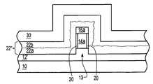
- FIG. 13shows the results of further processing of the semiconductor structure of FIG. 11 or FIG. 12 , since the pair of silicide layers 28 as illustrated in FIG. 12 is optional in the invention.
- FIG. 13shows a second stress imparting layer 30 located upon the recrystallized gate electrode 22 ′′.
- the second stress imparting layer 30may comprise stress imparting materials analogous, equivalent or identical to those utilized for the stress imparting layer 26 . It may also be formed utilizing methods that are analogous, equivalent or identical.
- the second stress imparting layer 30typically has a thickness from about 200 to about 1000 angstroms.
- the second stress imparting layer 30may have a third stress different from either: (1) the first stress closer to the semiconductor fin 14 a within the unamorphized sub-layer 22 a of the recrystallized gate electrode 22 ′′; or (2) the second stress further from the semiconductor fin 14 a within the recrystallized sub-layer 22 b ′ of the recrystallized gate electrode 22 ′′.
- the first stress, the second stress and the third stressmay define a continuous stress progression (either increasing or decreasing). Alternatively, they may define a discontinuous stress progression.
- Each of the first stress, second stress and third stressmay independently be a tensile stress or a compressive stress. Magnitudes of the first stress, second stress and third stress may also vary, but will typically range from about ⁇ 3.5 GPa to 2.5 GPa.
- FIG. 13shows a semiconductor structure further in accordance with a preferred embodiment of the invention.
- the semiconductor structureincludes a finFET structure that comprises the recrystallized gate electrode 22 ′′ having a first stress in a first region (i.e., unamorphized sub-layer 22 a ) located closer to the semiconductor fin 14 a therein and a second stress different than the first stress in a second region (i.e., recrystallized sub-layer 22 b ′) located further from the semiconductor fin 14 a .
- the finFET structurealso comprises the stress imparting layer 30 located over the recrystallized gate electrode 22 ′′.
- the stress imparting layer 30may have a third stress different from either the first stress or the second stress.
- the differing stress levels within multiple portions of the recrystallized gate electrode 22 ′′ within the finFET in accordance with the embodimentprovides for assistance in tuning stress within the semiconductor fin 14 a within the finFET. In turn, this may provide for enhanced finFET performance.
Landscapes
- Thin Film Transistor (AREA)
- Insulated Gate Type Field-Effect Transistor (AREA)
- Electroluminescent Light Sources (AREA)
- Electrodes Of Semiconductors (AREA)
Abstract
Description
- The invention relates generally to semiconductor structures. More particularly, the invention relates to enhanced semiconductor device performance through the use of mechanical stress effects and/or dopant redistribution effects within semiconductor structures.
- As semiconductor technology has advanced and semiconductor device density requirements have increased, there has been an increased need to fabricate semiconductor devices (e.g., MOSFET devices) with reduced dimensions, such as reduced gate electrode lengths of the devices. A novel semiconductor structure that accommodates increased density due to its considerably decreased dimensions is a double gate device that uses a finFET structure. A finFET structure provides a vertical channel device that includes a semiconductor fin set sideways upon a substrate. In order to obtain desirable control of short channel effects (SCEs), the semiconductor fin is thin enough in a device channel region to ensure forming fully depleted semiconductor devices. A pair of gate dielectric layers is typically located upon a pair of opposite semiconductor fin sidewalls. A gate electrode of an inverted U shape is typically located upon the semiconductor fin and covering the pair of gate dielectric layers. In some other instances, the gate electrode is not located atop the fin and thus it is restricted to the sidewalls of the fin.
- Beyond finFET structures that provide space efficient transistor structures with desirable SCE control, semiconductor devices are now commonly designed to use a mechanical stress effect (MSE) and/or a dopant redistribution or mobility effect to enhance transistor performance. The MSE is generally engineered to provide enhanced charge carrier mobility within a semiconductor device. The enhanced charge carrier mobility typically leads to enhanced semiconductor device performance.
- finFET structures may be fabricated with stressed components to improve performance of the finFET structures. For example, each of: (1) Rim, in U.S. Pat. No. 6,815,738; and (2) Lee et al., in Pub. No. 2004/0256647, teaches stressed semiconductor fin structures within finFETs. Each provides the stressed semiconductor fin structures by utilizing a lattice mismatch for layered components when forming the stressed semiconductor fin structures.
- Since desirable SCE control and space efficiency advantages of finFET devices are likely to continue to be of considerable significance within semiconductor device technology, and since stressed structures similarly also continue to provide semiconductor devices with enhanced performance, the utilization of stressed structures within finFETs is likely to continue.
- The invention provides a pair of finFET structures and a method for fabricating a finFET structure.
- The first of the pair of finFET structures includes a semiconductor fin located over a substrate. The structure also includes a gate electrode located over the semiconductor fin. Within the first structure, the gate electrode has a first stress in a first region located nearer the semiconductor fin and a second stress, which is different than the first stress, in a second region located further from the semiconductor fin.
- The second of the pair of finFET structures includes a semiconductor fin located over a pedestal within a substrate. Preferably, the semiconductor fin is located aligned over the pedestal within the substrate.
- The method derives from the first of the finFET structures. The method provides for forming a semiconductor fin over a substrate. It also provides for forming a gate electrode over the semiconductor fin, where the gate electrode has a first stress in a first region located nearer the semiconductor fin and a second stress, which is different than the first stress, in a second region located further from the semiconductor fin.
- The objects, features and advantages of the invention are understood within the context of the Description of the Preferred Embodiment, as set forth below. The Description of the Preferred Embodiment is understood within the context of the accompanying drawings, which form a material part of this disclosure, wherein:
FIG. 1 toFIG. 13 show a series of schematic cross-sectional and plan-view diagrams illustrating the results of progressive stages in fabricating a finFET structure in accordance with a preferred embodiment of the invention.- The invention provides a finFET structure with enhanced performance, and a method for fabricating the finFET structure.
FIG. 1 toFIG. 13 show a series of schematic cross-sectional and plan-view diagrams illustrating the results of progressive stages in fabricating a finFET structure in accordance with a preferred embodiment of the invention.- Specifically,
FIG. 1 shows asubstrate 10 having a burieddielectric layer 12 located thereupon. Asemiconductor layer 14 is located upon the burieddielectric layer 12. Ahard mask layer 16 is located upon thesemiconductor layer 14. Finally, a patternedphotoresist layer 18 is located upon thehard mask layer 18. - The
substrate 10 may comprise any of several materials, including but not limited to: a conductor material, a semiconductor material or a dielectric material. Typically, thesubstrate 10 comprises a semiconductor material. The semiconductor material may be selected from the group including, but not limited to: silicon (Si), germanium (Ge), silicon-germanium (SiGe) alloy, silicon carbide (SiC), silicon-germanium alloy carbide (SiGeC) and compound semiconductor materials, such as (III-VI) and (II-VI) semiconductor materials. Non-limiting examples of compound semiconductor materials include gallium arsenide, indium arsenide and indium phosphide materials. Typically, thesubstrate 10 has a thickness from about 1 to about 3 mils. - The buried
dielectric layer 12 typically comprises an oxide of a semiconductor material from which comprises thesubstrate 10, when thesubstrate 10 comprises a semiconductor material. Alternatively, the burieddielectric layer 12 may comprise a nitride, an oxynitride or an alternative dielectric material. The burieddielectric layer 12 may be formed utilizing methods as are conventional in the semiconductor fabrication art. Non-limiting examples of the methods include thermal annealing methods, chemical vapor deposition methods and physical vapor deposition methods. Typically, the burieddielectric layer 12 has a thickness from about 200 to about 10000 angstroms. - The
semiconductor layer 14 may comprise any of several semiconductor materials as are also conventional in the art. The semiconductor materials may include, but are not limited to: silicon, germanium, silicon-germanium alloy, silicon carbide, silicon-germanium alloy carbide, GaAs, InAs, InP, as well as other compound (III-V) and (II-VI) semiconductor materials. Thesemiconductor layer 14 may also comprise an organic semiconductor material. Typically, thesemiconductor layer 14 has a thickness from about 300 to about 1000 angstroms. - The substrate10 (when comprising a semiconductor material), the buried
dielectric layer 12 and thesemiconductor layer 14 comprise in an aggregate a semiconductor-on-insulator substrate. Within the embodiment and the invention, thesubstrate 10 typically comprises a silicon or silicon-germanium alloy semiconductor material, the burieddielectric layer 12 typically comprises a corresponding silicon or silicon-germanium oxide material and thesemiconductor layer 14 typically also comprises a corresponding silicon or silicon-germanium alloy semiconductor material. The semiconductor-on-insulator substrate may be formed utilizing any of several methods that are conventional in the semiconductor fabrication art. Non-limiting examples of such methods include layer transfer methods, laminating methods and, in particular, separation by implantation of oxygen (SIMOX) methods. - The
hard mask layer 16 comprises a hard mask material as is otherwise generally conventional in the art. Non-limiting examples of hard mask materials include oxides, nitrides and oxynitrides, typically of silicon and/or germanium, but oxides, nitrides and oxynitrides of other elements may also be utilized. The aforementioned hard mask materials may be deposited utilizing methods including, but not limited to: thermal annealing methods, chemical vapor deposition methods and physical vapor deposition sputtering methods. Typically, thehard mask layer 16 has a thickness from about 200 to about 400 angstroms, although such a thickness does not limit the embodiment or the invention. - The patterned
photoresist layer 18 may comprise photoresist materials that are conventional in the art. Non-limiting examples include positive photoresist materials, negative photoresist materials and hybrid photoresist materials. The resists may be processed to provide the patternedphotoresist layer 18 utilizing spin coating, photoexposure and development methods and materials as are conventional in the art. Typically, the patternedphotoresist layer 18 has a thickness from about 5000 to about 15000 angstroms. FIG. 2 shows the results of sequentially etching thehard mask layer 16, thesemiconductor layer 14 and, in part, the burieddielectric layer 12 to yield a corresponding patternedhard mask layer 16alocated aligned upon asemiconductor fin 14ain turn located aligned upon apedestal 13 within an etched burieddielectric layer 12′. Typically, thepedestal 13 has a height from about 200 to about 400 angstroms within the etched burieddielectric layer 12′. The foregoing etching of at least thehard mask layer 16 to form the patternedhard mask layer 16ais effected while utilizing the patternedphotoresist layer 18 as an etch mask. The patternedhard mask layer 16a, with or without the patterned photoresist layer18a, is utilized when patterning thesemiconductor fin 14afrom thesemiconductor layer 14 and typically also when etching the burieddielectric layer 12 to form the etched burieddielectric layer 12′.- The foregoing layers are preferably etched anisotropically to thus provide substantially straight sidewalls. Such etching typically utilizes a reactive ion etch plasma etchant or another anisotropic etchant, such as an ion beam etchant. Wet chemical etchant materials, while typically less common, may under certain circumstances also be utilized, although they are generally isotropic etchants. When utilizing a reactive ion etch plasma etchant, a fluorine containing etchant gas composition is typically utilized when etching a silicon containing hard mask material or a silicon containing dielectric material. A chlorine containing etchant gas composition is typically utilized when etching a silicon or germanium containing semiconductor material.
FIG. 3 shows a pair of gate dielectric layers20 located upon a pair of opposite sidewalls of thesemiconductor fin 14a. The pair of gate dielectric layers20 typically comprises a thermal oxide of a semiconductor material which comprises thesemiconductor fin 14a. When thermal techniques are used, the gate dielectric layers20 are formed within a surface portion of thesemiconductor fin 14a, as shown. Alternatively, deposited dielectric materials rather than thermally grown dielectric materials may also be utilized. When deposited dielectrics are used, the gate dielectric would generally be present on the sidewalls and over a top portion of thesemiconductor fin 14a. Such alternative deposited dielectric materials may include, but are not limited to: other silicon oxides, nitrides and oxynitrides that typically have a dielectric constant from about 4 to about 20 as measured in vacuum; as well as heavier metal oxides such as hafnium oxides, hafnium silicates, aluminum oxides, titanium oxides, lanthanum oxides, barium-strontium-titanate (BST), lead-zirconate-titanate (PZT) and other ferroelectric materials. The heavier metal oxides typically have a dielectric constant greater than about 20 and perhaps as high as at least 100. Typically, each of the pair of gate dielectric layers20 has a thickness from about 10 to about 20 angstroms when comprised of a thermal silicon oxide material.FIG. 4 shows agate electrode 22 of inverted U shape located over thesemiconductor fin 14aand upon the etched burieddielectric layer 12′, the pair of gate dielectric layers20 and the patternedhard mask layer 16a. Thegate electrode 22 typically comprises a doped polysilicon material (i.e., dopant concentration from about 1e18 to 1e20 dopant atoms per cubic centimeter). Alternative gate electrode conductor materials may be utilized provided that they are in a nominally crystalline or otherwise ordered state that is susceptible to decrystallization or amorphization or other processing to provide a depth specific amorphous or otherwise non-crystalline region. Such other conductor materials may thus include, but are not limited to: certain metals, metal alloys, metal nitrides and metal silicides. Thegate electrode 22 may be formed utilizing deposition and patterning methods as are otherwise generally conventional in the art. Non-limiting examples include chemical vapor deposition methods and physical vapor deposition methods. Typically, thegate electrode 22 has a thickness from about 800 to about 1500 angstroms.FIG. 5 shows a schematic plan-view diagram of a semiconductor structure corresponding with the semiconductor structure ofFIG. 4 .FIG. 5 shows the etched burieddielectric layer 12′. The patternedhard mask layer 16ain a dogbone shape is located over the etched burieddielectric layer 12′. Aligned beneath the patternedhard mask layer 16ais thesemiconductor fin 14aand the pair of gate dielectric layers20.Elements FIG. 5 . Thegate electrode 22 traverses thesemiconductor fin 14aand the overlying patternedhard mask layer 16aat the center thereof. The portion of thesemiconductor fin 14acovered by thegate electrode 22 comprises a channel region. The end portions of thesemiconductor fin 14auncovered by thegate electrode 22 comprises a region where a pair of source/drain regions can subsequently be located and formed. The dogbone shape of both the patternedhard mask layer 16aand thesemiconductor fin 14aaligned therebeneath is intended to have a central axial portion that extends to a pair of lobed ends of linewidth greater than the central axial portion. The central axial portion may have a linewidth from about 0.05 to about 0.30 microns, although neither the embodiment nor the invention is so limited to such a linewidth range.FIG. 5 illustrates the lobed ends of the patternedhard mask layer 16adogbone as particularly angular, but in a discrete finFET structure as illustrated inFIG. 5 lobed ends may alternatively have less angular features.- Similarly, while the schematic plan-view diagram of
FIG. 5 illustrates a finFET in accordance with the instant embodiment as a discrete device having a single semiconductor fin and gate electrode, such a particular structure does not limit the embodiment or the invention. Rather, embodiments are also contemplated where multiple finFET devices may be linked with a single elongated spanning gate electrode (such as gate electrode22) in one or both directions. Also, multiple devices may be linked through alternatively spanning semiconductor fins (such assemiconductor fin 14a) in one or both directions. FIG. 6 shows a schematic cross-sectional diagram through a source/drain extension region of thesemiconductor fin 14ain accordance with the cross-sectional reference plane6-6 illustrated inFIG. 5 .FIG. 6 shows thesemiconductor fin 14alocated upon thepedestal 13 within the etched burieddielectric layer 12′.FIG. 6 also shows the pair of gate dielectric layers20 located upon opposite sidewalls of thesemiconductor fin 14a, and the patternedhard mask layer 16alocated atop thesemiconductor fin 14a. Finally,FIG. 6 shows a dose of first implantingions 21 that is used for forming an extension implant and/or a halo implant located within the extension region. The dose of first implantingions 21 is provided at a tilt angle typically from about 30° to about 45° with respect to the major plane of the etched burieddielectric layer 12′, and also at a concentration conventional in the finFET fabrication art. The dose of first implantingions 21 also has a polarity appropriate to the polarity of the finFET desired to be fabricated.FIG. 7 shows a schematic cross-sectional diagram illustrating the results of further processing of the finFET whose schematic cross-sectional diagram is illustrated inFIG. 6 .FIG. 7 shows acontiguous spacer layer 16′ that covers the sidewalls of the pair of gate dielectric layers20 and incorporates the patternedhard mask layer 16aas illustrated inFIG. 6 . Typically, thecontiguous spacer layer 16′ comprises a spacer material analogous, equivalent or identical to the hard mask material from which is comprised the patternedhard mask layer 16a. Typical non-limiting materials include oxides, nitrides and oxynitrides. Typically, thecontiguous spacer layer 16′ is formed using a blanket layer (i.e., from about 300 to about 500 angstrom thickness) deposition step, followed by an anisotropic etchback step. Chemical vapor deposition methods (thermally activated and plasma activated) and physical deposition methods may be used for the blanket layer deposition. Other methods are not precluded.- The
contiguous spacer layer 16′ as illustrated inFIG. 7 inhibits undesirable ion implant damage to the source/drain and extension regions within thesemiconductor fin layer 14aincident to further amorphizing ion implant processing of the semiconductor structure whose schematic cross-sectional diagram is illustrated inFIG. 4 . Thus, both the extension and halo ion implant processing as illustrated inFIG. 6 and the contiguous spacer layer processing as illustrated inFIG. 7 are typically effected prior to additional amorphizing ion implant processing of the semiconductor structure ofFIG. 4 , in accordance with the embodiment and the invention. FIG. 8 shows the results of such additional amorphizing ion implant processing of the semiconductor structure ofFIG. 4 as viewed through the cross-section reference plane4-4 illustrated inFIG. 5 . Again, the additional amorphizing ion implant processing is typically effected after the processing illustrated inFIG. 6 andFIG. 7 .FIG. 8 shows the results of ion implanting thegate electrode 22 to form a partiallyamorphized gate electrode 22′. The partiallyamorphized gate electrode 22′ comprises anunamorphized sub-layer 22alocated nearer thesemiconductor fin 14a. The partiallyamorphized gate electrode 22′ also comprises anamorphized sub-layer 22bas a surface layer located further from thesemiconductor fin 14a. The partiallyamorphized gate electrode 22′ is amorphized to a distance that corresponds with the thickness of theamorphized sub-layer 22b. The distance is preferably deeper than an interface of thesemiconductor fin 14awith the etched burieddielectric layer 12′. Amorphization is effected utilizing a dose ofamorphizing ions 23. The dose ofamorphizing ions 23 is preferably of a variety that also includes dopant ions insofar as the amorphizing ions may also be utilized for doping certain portions of the source/drain regions within thesemiconductor fin 14athat are not covered by the partiallyamorphized gate electrode 22′ as illustrated inFIG. 8 , or thicker portions of thecontiguous spacer layer 16′ as illustrated inFIG. 7 . Theamorphizing ions 23 may similarly also include non-dopant amorphizing ions such as germanium amorphizing ions. Other heavier non-amorphizing ions may also be used. Typically, an aggregate concentration ofamorphizing ions 23, including dopant and non-dopant amorphizing ions, is from about 1e18 to about 1e22 dopant atoms per cubic centimeter. Theamorphizing ions 23 are preferably provided at a tilt angle of from about 30° to about 45° as illustrated inFIG. 6 , although this is not required in either the instant embodiment or in the invention.FIG. 9 shows apad dielectric layer 24 located upon the partiallyamorphized gate electrode 22′, and also astress imparting layer 26 located upon thepad dielectric layer 24.- The
pad dielectric layer 24 typically comprises any of several dielectric materials as are conventionally utilized for a pad dielectric layer. Non-limiting examples include silicon oxide, silicon nitride and silicon oxynitride materials. Silicon oxide materials are particularly common. Thepad dielectric layer 24 may be formed utilizing any of several methods as are convention in the art. Non-limiting examples include thermal oxidation methods, chemical vapor deposition methods and physical vapor deposition methods. Preferably, thepad dielectric layer 24 is formed utilizing a thermal oxidation method to yield a silicon oxide material. Typically, thepad dielectric layer 24 has a thickness from about 10 to about 100 angstroms. - The
stress imparting layer 26 may comprise any of several stress imparting materials, but from a practical perspective the stress imparting material must have thermal resistance characteristics that allow for higher temperature annealing absent deterioration of the stress imparting layer or any layers therebeneath. Non-limiting examples of stress imparting materials include silicon nitride materials and silicon oxynitride materials. Silicon nitride materials are particularly preferred. Thestress imparting layer 26 may have either a positive stress or a negative stress as appropriate for either an n-finFET or a p-finFET. - Also from a practical perspective, there are several process variables that may be utilized to influence stress when forming the
stress imparting layer 26. Non-limiting examples include deposition temperature, starting materials, deposition rate and thickness. Typically, the stress imparting layer has a thickness from about 500 to about 2000 angstroms, although neither the embodiment nor the invention is so limited. FIG. 10 shows the results of thermally annealing the semiconductor structure ofFIG. 9 . Incident to the thermal annealing, the partiallyamorphized gate electrode 22′ recrystallizes to yield a recrystallizedgate electrode 22″. Within the context of the instant embodiment, recrystallization of the partiallyamorphized gate electrode 22′ to yield the recrystallizedgate electrode 22″ coincidentally involves recrystallization of theamorphized sub-layer 22bto provide a recrystallizedsub-layer 22b′. When the partiallyamorphized gate electrode 22′ recrystallizes to yield the recrystallizedgate electrode 22″, it does so (i.e., in particular with respect to theamorphized sub-layer 22b) under the influence of the stress condition of thestress imparting layer 26. Thus, the recrystallizedgate electrode 22″ has a first stress in a first portion or region located nearer thesemiconductor fin 14aand the etched burieddielectric layer 12′ (i.e., theunamorphized sub-layer 22awhich is formed with an initial stress level) and a second stress different than the first stress in a separate second portion or region further from thesemiconductor fin 14aand the etched burieddielectric layer 12′ (i.e., the recrystallizedsub-layer 22b′). Moreover, during the recrystallization and its attendant thermal annealing, dopants contained in the partiallyamorphized gate electrode 22′ and thesemiconductor fin 14awill redistribute within the context of the stress imparted fromstress imparting layer 26 into theamorphized sub-layer 22b. This type and mechanism of dopant redistribution can also enhance finFET device performance.- With respect to the recrystallized
gate electrode 22′, the first stress therein may be less than the second stress or the first stress may be greater than the second stress. The first stress and the second stress may be both compressive or both tensile. Alternatively, one of the first stress and the second stress may be tensile and the other of the first stress and the second stress may be compressive. - Recrystallization of the partially
amorphized gate electrode 22′ to form the recrystallizedgate electrode 22″ may be undertaken utilizing any of several thermal annealing methods that are conventional in the semiconductor fabrication art. Non-limiting examples include furnace annealing methods and rapid thermal annealing methods. Typically, but not exclusively, the partiallyamorphized gate electrode 22′ is thermally annealed at a temperature from about 1000° to about 1200° C. for a time period from about 2 to about 6 hours. Typically, the thermal annealing is undertaken in an inert atmosphere, such as a helium, argon, krypton or nitrogen atmosphere, although this is not required. As is understood by a person skilled in the art, the foregoing thermal annealing conditions also provide for a recrystallizing of source/drain regions of thesemiconductor fin 14aand a drive-in of active dopants implanted therein. FIG. 11 shows the results of sequentially stripping thestress imparting layer 26 and thepad dielectric layer 24 from the semiconductor structure ofFIG. 10 . Upon stripping, they leave exposed the recrystallizedgate electrode 22″. They may be sequentially stripped while utilizing methods and materials that are conventional in the semiconductor fabrication art. In particular, but without limitation, for silicon nitride or silicon oxynitride materials aqueous phosphoric acid materials may be utilized. Also without limitation, for silicon oxide materials aqueous hydrofluoric acid materials may be utilized. Other appropriate wet chemical etch materials and dry plasma etch materials may also be utilized.FIG. 11 shows in a first instance a semiconductor structure in accordance with a preferred embodiment of the invention. In a first instance, the semiconductor structure comprises asemiconductor fin 14aaligned upon apedestal 13 within an etched burieddielectric layer 12′. Thepedestal 13 spaces thesemiconductor fin 14aabove surrounding portions of the etched burieddielectric layer 12′. Due to the spacing the recrystallizedgate electrode 22″ subsequently located and formed upon thesemiconductor fin 14ais so located with a more complete overlap. Within the finFET structure in accordance withFIG. 11 the recrystallizedgate electrode 22″ has multiple regions with different stress. The multiple regions include a first region located closer thesemiconductor fin 14aand having a first stress, as well as a second region located further from thesemiconductor fin 14aand having a second stress different than the first stress.- Although the preferred embodiment illustrates the invention with the recrystallized
gate electrode 22″ having two regions of different stress, neither the instant embodiment nor the invention is so limited. Rather, as is understood by a person skilled in the art the invention may be practiced with sequentially less and less deep ion implant amorphizations of a gate electrode, along with concurrent and sequential recrystallizations under multiple sequential stress imparting layer influence. The foregoing process sequence yields further additionally defined stress regions within a multiply recrystallized gate electrode. FIG. 12 shows a schematic plan-view diagram illustrating the results of further processing of the finFET ofFIG. 11 .FIG. 12 also corresponds withFIG. 5 , but with a pair ofsilicide layers 28 located upon source/drain regions of thesemiconductor fin layer 14anot covered by the recrystallizedgate electrode 22″. To provide the finFET structure ofFIG. 12 in comparison with the finFET structure ofFIG. 5 , portions of the patternedhard mask layer 16alocated upon regions of thesemiconductor fin 14anot covered by the recrystallizedgate electrode 22″ are removed. They may be removed utilizing etch methods as are conventional in the semiconductor fabrication art. The methods may include, but are not limited to: wet chemical etch methods and dry plasma etch methods.- Once source/drain region portions of the
semiconductor fin 14aare exposed, the pair ofsilicide layers 28 may be formed utilizing methods as are also conventional in the art. Typically, the pair of silicide layers28 is formed utilizing a metal silicide forming metal layer deposition, thermal annealing and subsequent unreacted metal etch method (i.e., a salicide method). Alternative methods may be employed. Typical metal silicide forming metals include, but are not limited to: tungsten, cobalt, platinum, nickel and titanium. Thermal annealing conditions are typically about 350° to about 850° C. for a time period from about 1 second to about 10 minutes. Unreacted metal etchants are specific to particular metals and are typically wet chemical etchants, although this is not a requirement of the invention. Typically, each of the pair of silicide layers28 has a thickness from about 50 to about 300 angstroms. They are optional within the invention. FIG. 13 shows the results of further processing of the semiconductor structure ofFIG. 11 orFIG. 12 , since the pair ofsilicide layers 28 as illustrated inFIG. 12 is optional in the invention.FIG. 13 shows a secondstress imparting layer 30 located upon the recrystallizedgate electrode 22″. The secondstress imparting layer 30 may comprise stress imparting materials analogous, equivalent or identical to those utilized for thestress imparting layer 26. It may also be formed utilizing methods that are analogous, equivalent or identical. The secondstress imparting layer 30 typically has a thickness from about 200 to about 1000 angstroms.- Within the instant embodiment, the second
stress imparting layer 30 may have a third stress different from either: (1) the first stress closer to thesemiconductor fin 14awithin theunamorphized sub-layer 22aof the recrystallizedgate electrode 22″; or (2) the second stress further from thesemiconductor fin 14awithin the recrystallizedsub-layer 22b′ of the recrystallizedgate electrode 22″. The first stress, the second stress and the third stress may define a continuous stress progression (either increasing or decreasing). Alternatively, they may define a discontinuous stress progression. Each of the first stress, second stress and third stress may independently be a tensile stress or a compressive stress. Magnitudes of the first stress, second stress and third stress may also vary, but will typically range from about −3.5 GPa to 2.5 GPa. FIG. 13 shows a semiconductor structure further in accordance with a preferred embodiment of the invention. The semiconductor structure includes a finFET structure that comprises the recrystallizedgate electrode 22″ having a first stress in a first region (i.e., unamorphized sub-layer22a) located closer to thesemiconductor fin 14atherein and a second stress different than the first stress in a second region (i.e., recrystallizedsub-layer 22b′) located further from thesemiconductor fin 14a. The finFET structure also comprises thestress imparting layer 30 located over the recrystallizedgate electrode 22″. Thestress imparting layer 30 may have a third stress different from either the first stress or the second stress. The differing stress levels within multiple portions of the recrystallizedgate electrode 22″ within the finFET in accordance with the embodiment provides for assistance in tuning stress within thesemiconductor fin 14awithin the finFET. In turn, this may provide for enhanced finFET performance.- The preferred embodiment of the invention is illustrative of the invention rather than limiting of the invention. Revisions and modifications may be made to methods, materials, structures and dimensions in accordance with the preferred embodiment of the invention while still providing an embodiment in accordance with the invention, further in accordance with the accompanying claims.
Claims (20)
Priority Applications (4)
| Application Number | Priority Date | Filing Date | Title |
|---|---|---|---|
| US11/164,621US7564081B2 (en) | 2005-11-30 | 2005-11-30 | finFET structure with multiply stressed gate electrode |
| CNA2006101395598ACN1976059A (en) | 2005-11-30 | 2006-09-26 | Fin type field effect transistor structure and method of manufacturing the same |
| JP2006317780AJP5186101B2 (en) | 2005-11-30 | 2006-11-24 | FinFET structure with multi-stressed gate electrode |
| US12/505,894US8058157B2 (en) | 2005-11-30 | 2009-07-20 | FinFET structure with multiply stressed gate electrode |
Applications Claiming Priority (1)
| Application Number | Priority Date | Filing Date | Title |
|---|---|---|---|
| US11/164,621US7564081B2 (en) | 2005-11-30 | 2005-11-30 | finFET structure with multiply stressed gate electrode |
Related Child Applications (1)
| Application Number | Title | Priority Date | Filing Date |
|---|---|---|---|
| US12/505,894DivisionUS8058157B2 (en) | 2005-11-30 | 2009-07-20 | FinFET structure with multiply stressed gate electrode |
Publications (2)
| Publication Number | Publication Date |
|---|---|
| US20070120154A1true US20070120154A1 (en) | 2007-05-31 |
| US7564081B2 US7564081B2 (en) | 2009-07-21 |
Family
ID=38086598
Family Applications (2)
| Application Number | Title | Priority Date | Filing Date |
|---|---|---|---|
| US11/164,621Active2026-05-05US7564081B2 (en) | 2005-11-30 | 2005-11-30 | finFET structure with multiply stressed gate electrode |
| US12/505,894Active2026-04-02US8058157B2 (en) | 2005-11-30 | 2009-07-20 | FinFET structure with multiply stressed gate electrode |
Family Applications After (1)
| Application Number | Title | Priority Date | Filing Date |
|---|---|---|---|
| US12/505,894Active2026-04-02US8058157B2 (en) | 2005-11-30 | 2009-07-20 | FinFET structure with multiply stressed gate electrode |
Country Status (3)
| Country | Link |
|---|---|
| US (2) | US7564081B2 (en) |
| JP (1) | JP5186101B2 (en) |
| CN (1) | CN1976059A (en) |
Cited By (23)
| Publication number | Priority date | Publication date | Assignee | Title |
|---|---|---|---|---|
| US20080171408A1 (en)* | 2007-01-12 | 2008-07-17 | International Business Machines Corporation | Methods for forming dual fully silicided gates over fins of finfet devices |
| US20080303096A1 (en)* | 2007-06-07 | 2008-12-11 | Thomas Schulz | Semiconductor devices and methods of manufacture thereof |
| US20090072316A1 (en)* | 2007-09-14 | 2009-03-19 | Advanced Micro Devices, Inc. | Double layer stress for multiple gate transistors |
| US20100140722A1 (en)* | 2006-08-31 | 2010-06-10 | Richard Lindsay | Strained Semiconductor Device and Method of Making Same |
| US20100308409A1 (en)* | 2009-06-08 | 2010-12-09 | Globalfoundries Inc. | Finfet structures with fins having stress-inducing caps and methods for fabricating the same |
| US20110210393A1 (en)* | 2010-03-01 | 2011-09-01 | Taiwan Semiconductor Manufacturing Co., Ltd. | Dual epitaxial process for a finfet device |
| US20120018730A1 (en)* | 2010-07-22 | 2012-01-26 | International Business Machines Corporation | Structure and method for stress latching in non-planar semiconductor devices |
| US8513066B2 (en)* | 2005-10-25 | 2013-08-20 | Freescale Semiconductor, Inc. | Method of making an inverted-T channel transistor |
| US8643066B2 (en) | 2005-10-25 | 2014-02-04 | Freescale Semiconductor, Inc. | Multiple device types including an inverted-T channel transistor and method therefor |
| US8722494B1 (en) | 2012-11-01 | 2014-05-13 | International Business Machines Corporation | Dual gate finFET devices |
| US20140252502A1 (en)* | 2013-03-11 | 2014-09-11 | International Business Machines Corporation | Multilayer dielectric structures for semiconductor nano-devices |
| US20140273369A1 (en)* | 2013-03-13 | 2014-09-18 | Globalfoundries Inc. | Methods of forming contacts to source/drain regions of finfet devices |
| US20150145048A1 (en)* | 2013-11-22 | 2015-05-28 | International Business Machines Corporation | Structure and method for forming cmos with nfet and pfet having different channel materials |
| US20150303305A1 (en)* | 2014-04-16 | 2015-10-22 | Taiwan Semiconductor Manufacturing Company, Ltd. | FinFET Device with High-K Metal Gate Stack |
| US9171904B2 (en) | 2012-12-05 | 2015-10-27 | Imec | FinFET device with dual-strained channels and method for manufacturing thereof |
| US20150371889A1 (en)* | 2014-06-20 | 2015-12-24 | Applied Materials, Inc. | Methods for shallow trench isolation formation in a silicon germanium layer |
| US20160005813A1 (en)* | 2014-07-02 | 2016-01-07 | Sang-Su Kim | Fin structures and methods of manfacturing the fin structures, and fin transistors having the fin structures and methods of manufacturing the fin transistors |
| CN105405890A (en)* | 2015-11-05 | 2016-03-16 | 中国科学院微电子研究所 | Semiconductor device including charged body sidewall and method of manufacturing the same |
| CN105448985A (en)* | 2014-08-14 | 2016-03-30 | 中国科学院微电子研究所 | Semiconductor device and method for manufacturing the same |
| US9312179B2 (en) | 2010-03-17 | 2016-04-12 | Taiwan-Semiconductor Manufacturing Co., Ltd. | Method of making a finFET, and finFET formed by the method |
| US9559181B2 (en) | 2013-11-26 | 2017-01-31 | Taiwan Semiconductor Manufacturing Company, Ltd. | Structure and method for FinFET device with buried sige oxide |
| US11205594B2 (en) | 2013-01-14 | 2021-12-21 | Taiwan Semiconductor Manufacturing Company, Ltd. | Fin spacer protected source and drain regions in FinFETs |
| US11563118B2 (en) | 2014-06-27 | 2023-01-24 | Taiwan Semiconductor Manufacturing Company, Ltd. | Structure and method for SRAM FinFET device |
Families Citing this family (33)
| Publication number | Priority date | Publication date | Assignee | Title |
|---|---|---|---|---|
| JP2008010503A (en)* | 2006-06-27 | 2008-01-17 | Toshiba Corp | Semiconductor memory device and manufacturing method thereof |
| US7928426B2 (en)* | 2007-03-27 | 2011-04-19 | Intel Corporation | Forming a non-planar transistor having a quantum well channel |
| JP4575471B2 (en)* | 2008-03-28 | 2010-11-04 | 株式会社東芝 | Semiconductor device and manufacturing method of semiconductor device |
| JP5285947B2 (en)* | 2008-04-11 | 2013-09-11 | 株式会社東芝 | Semiconductor device and manufacturing method thereof |
| US8912602B2 (en)* | 2009-04-14 | 2014-12-16 | Taiwan Semiconductor Manufacturing Company, Ltd. | FinFETs and methods for forming the same |
| US8236709B2 (en)* | 2009-07-29 | 2012-08-07 | International Business Machines Corporation | Method of fabricating a device using low temperature anneal processes, a device and design structure |
| US20110068348A1 (en)* | 2009-09-18 | 2011-03-24 | Taiwan Semiconductor Manufacturing Company, Ltd. | Thin body mosfet with conducting surface channel extensions and gate-controlled channel sidewalls |
| US8344425B2 (en)* | 2009-12-30 | 2013-01-01 | Intel Corporation | Multi-gate III-V quantum well structures |
| US8338280B2 (en)* | 2010-07-08 | 2012-12-25 | Globalfoundries Singapore Pte. Ltd. | Method for fabricating nano devices |
| CN102456734B (en)* | 2010-10-29 | 2015-06-10 | 中国科学院微电子研究所 | Semiconductor structure and manufacturing method thereof |
| US8778744B2 (en)* | 2011-06-24 | 2014-07-15 | Institute of Microelectronics, Chinese Academy of Sciences | Method for manufacturing semiconductor field effect transistor |
| CN103187439B (en) | 2011-12-29 | 2015-08-05 | 中芯国际集成电路制造(上海)有限公司 | Semiconductor structure and forming method thereof, CMOS and forming method thereof |
| US20130200455A1 (en) | 2012-02-08 | 2013-08-08 | Taiwan Semiconductor Manufacturing Company, Ltd. | Dislocation smt for finfet device |
| US8629559B2 (en) | 2012-02-09 | 2014-01-14 | Taiwan Semiconductor Manufacturing Company, Ltd. | Stress reduction apparatus with an inverted cup-shaped layer |
| CN103296068B (en)* | 2012-03-02 | 2016-03-16 | 中芯国际集成电路制造(上海)有限公司 | Cmos and forming method thereof |
| CN103681846B (en)* | 2012-09-20 | 2017-02-08 | 中芯国际集成电路制造(上海)有限公司 | Semiconductor device and manufacturing method thereof |
| US8766363B2 (en)* | 2012-11-07 | 2014-07-01 | International Business Machines Corporation | Method and structure for forming a localized SOI finFET |
| US9034716B2 (en)* | 2013-01-31 | 2015-05-19 | Taiwan Semiconductor Manufacturing Company, Ltd. | Method of making a FinFET device |
| FR3003691B1 (en)* | 2013-03-19 | 2016-07-01 | Soitec Silicon On Insulator | FINFET WITH REAR GRILLE |
| US9040363B2 (en) | 2013-03-20 | 2015-05-26 | International Business Machines Corporation | FinFET with reduced capacitance |
| CN105164809B (en)* | 2013-06-26 | 2018-07-24 | 美商新思科技有限公司 | FinFETs with heterojunction and improved channel control |
| US9105662B1 (en) | 2014-01-23 | 2015-08-11 | International Business Machines Corporation | Method and structure to enhance gate induced strain effect in multigate device |
| US9373706B2 (en) | 2014-01-24 | 2016-06-21 | Samsung Electronics Co., Ltd. | Methods of forming semiconductor devices, including forming a semiconductor material on a fin, and related semiconductor devices |
| US9502565B2 (en) | 2014-06-27 | 2016-11-22 | Taiwan Semiconductor Manufacturing Company, Ltd. | Channel strain control for nonplanar compound semiconductor devices |
| US9306067B2 (en) | 2014-08-05 | 2016-04-05 | Taiwan Semiconductor Manufacturing Company, Ltd. | Nonplanar device and strain-generating channel dielectric |
| US9941406B2 (en) | 2014-08-05 | 2018-04-10 | Taiwan Semiconductor Manufacturing Company, Ltd. | FinFETs with source/drain cladding |
| KR20160018221A (en)* | 2014-08-08 | 2016-02-17 | 에스케이하이닉스 주식회사 | 3 Dimension Semiconductor Integrated Circuit Device And Method of Manufacturing The Same |
| US9263587B1 (en)* | 2014-09-04 | 2016-02-16 | Globalfoundries Inc. | Fin device with blocking layer in channel region |
| US9577101B2 (en) | 2015-03-13 | 2017-02-21 | Taiwan Semiconductor Manufacturing Company, Ltd. | Source/drain regions for fin field effect transistors and methods of forming same |
| US9362311B1 (en) | 2015-07-24 | 2016-06-07 | Samsung Electronics Co., Ltd. | Method of fabricating semiconductor device |
| CN107492501B (en)* | 2016-06-13 | 2020-03-10 | 中芯国际集成电路制造(上海)有限公司 | Method for forming fin field effect transistor |
| US9680019B1 (en)* | 2016-07-20 | 2017-06-13 | Globalfoundries Inc. | Fin-type field-effect transistors with strained channels |
| US11164876B2 (en)* | 2019-02-07 | 2021-11-02 | Micron Technology, Inc. | Atom implantation for passivation of pillar material |
Citations (80)
| Publication number | Priority date | Publication date | Assignee | Title |
|---|---|---|---|---|
| US3602841A (en)* | 1970-06-18 | 1971-08-31 | Ibm | High frequency bulk semiconductor amplifiers and oscillators |
| US4665415A (en)* | 1985-04-24 | 1987-05-12 | International Business Machines Corporation | Semiconductor device with hole conduction via strained lattice |
| US4853076A (en)* | 1983-12-29 | 1989-08-01 | Massachusetts Institute Of Technology | Semiconductor thin films |
| US4855245A (en)* | 1985-09-13 | 1989-08-08 | Siemens Aktiengesellschaft | Method of manufacturing integrated circuit containing bipolar and complementary MOS transistors on a common substrate |
| US4952524A (en)* | 1989-05-05 | 1990-08-28 | At&T Bell Laboratories | Semiconductor device manufacture including trench formation |
| US4958213A (en)* | 1987-12-07 | 1990-09-18 | Texas Instruments Incorporated | Method for forming a transistor base region under thick oxide |
| US5006913A (en)* | 1988-11-05 | 1991-04-09 | Mitsubishi Denki Kabushiki Kaisha | Stacked type semiconductor device |
| US5060030A (en)* | 1990-07-18 | 1991-10-22 | Raytheon Company | Pseudomorphic HEMT having strained compensation layer |
| US5081513A (en)* | 1991-02-28 | 1992-01-14 | Xerox Corporation | Electronic device with recovery layer proximate to active layer |
| US5108843A (en)* | 1988-11-30 | 1992-04-28 | Ricoh Company, Ltd. | Thin film semiconductor and process for producing the same |
| US5134085A (en)* | 1991-11-21 | 1992-07-28 | Micron Technology, Inc. | Reduced-mask, split-polysilicon CMOS process, incorporating stacked-capacitor cells, for fabricating multi-megabit dynamic random access memories |
| US5310446A (en)* | 1990-01-10 | 1994-05-10 | Ricoh Company, Ltd. | Method for producing semiconductor film |
| US5354695A (en)* | 1992-04-08 | 1994-10-11 | Leedy Glenn J | Membrane dielectric isolation IC fabrication |
| US5371399A (en)* | 1991-06-14 | 1994-12-06 | International Business Machines Corporation | Compound semiconductor having metallic inclusions and devices fabricated therefrom |
| US5391510A (en)* | 1992-02-28 | 1995-02-21 | International Business Machines Corporation | Formation of self-aligned metal gate FETs using a benignant removable gate material during high temperature steps |
| US5459346A (en)* | 1988-06-28 | 1995-10-17 | Ricoh Co., Ltd. | Semiconductor substrate with electrical contact in groove |
| US5557122A (en)* | 1995-05-12 | 1996-09-17 | Alliance Semiconductors Corporation | Semiconductor electrode having improved grain structure and oxide growth properties |
| US5561302A (en)* | 1994-09-26 | 1996-10-01 | Motorola, Inc. | Enhanced mobility MOSFET device and method |
| US5670798A (en)* | 1995-03-29 | 1997-09-23 | North Carolina State University | Integrated heterostructures of Group III-V nitride semiconductor materials including epitaxial ohmic contact non-nitride buffer layer and methods of fabricating same |
| US5679965A (en)* | 1995-03-29 | 1997-10-21 | North Carolina State University | Integrated heterostructures of Group III-V nitride semiconductor materials including epitaxial ohmic contact, non-nitride buffer layer and methods of fabricating same |
| US5861651A (en)* | 1997-02-28 | 1999-01-19 | Lucent Technologies Inc. | Field effect devices and capacitors with improved thin film dielectrics and method for making same |
| US5880040A (en)* | 1996-04-15 | 1999-03-09 | Macronix International Co., Ltd. | Gate dielectric based on oxynitride grown in N2 O and annealed in NO |
| US5940736A (en)* | 1997-03-11 | 1999-08-17 | Lucent Technologies Inc. | Method for forming a high quality ultrathin gate oxide layer |
| US5960297A (en)* | 1997-07-02 | 1999-09-28 | Kabushiki Kaisha Toshiba | Shallow trench isolation structure and method of forming the same |
| US5989978A (en)* | 1998-07-16 | 1999-11-23 | Chartered Semiconductor Manufacturing, Ltd. | Shallow trench isolation of MOSFETS with reduced corner parasitic currents |
| US6008126A (en)* | 1992-04-08 | 1999-12-28 | Elm Technology Corporation | Membrane dielectric isolation IC fabrication |
| US6025280A (en)* | 1997-04-28 | 2000-02-15 | Lucent Technologies Inc. | Use of SiD4 for deposition of ultra thin and controllable oxides |
| US6066545A (en)* | 1997-12-09 | 2000-05-23 | Texas Instruments Incorporated | Birdsbeak encroachment using combination of wet and dry etch for isolation nitride |
| US6090684A (en)* | 1998-07-31 | 2000-07-18 | Hitachi, Ltd. | Method for manufacturing semiconductor device |
| US6107143A (en)* | 1998-03-02 | 2000-08-22 | Samsung Electronics Co., Ltd. | Method for forming a trench isolation structure in an integrated circuit |
| US6117722A (en)* | 1999-02-18 | 2000-09-12 | Taiwan Semiconductor Manufacturing Company | SRAM layout for relaxing mechanical stress in shallow trench isolation technology and method of manufacture thereof |
| US6133071A (en)* | 1997-10-15 | 2000-10-17 | Nec Corporation | Semiconductor device with plate heat sink free from cracks due to thermal stress and process for assembling it with package |
| US6165383A (en)* | 1998-04-10 | 2000-12-26 | Organic Display Technology | Useful precursors for organic electroluminescent materials and devices made from such materials |
| US6180501B1 (en)* | 1999-10-14 | 2001-01-30 | Chartered Semiconductor Manufacturing Ltd. | Method to fabricate a double-polysilicon gate structure for a sub-quarter micron self-aligned-titanium silicide process |
| US6221735B1 (en)* | 2000-02-15 | 2001-04-24 | Philips Semiconductors, Inc. | Method for eliminating stress induced dislocations in CMOS devices |
| US6228694B1 (en)* | 1999-06-28 | 2001-05-08 | Intel Corporation | Method of increasing the mobility of MOS transistors by use of localized stress regions |
| US6255169B1 (en)* | 1999-02-22 | 2001-07-03 | Advanced Micro Devices, Inc. | Process for fabricating a high-endurance non-volatile memory device |
| US6261964B1 (en)* | 1997-03-14 | 2001-07-17 | Micron Technology, Inc. | Material removal method for forming a structure |
| US6265317B1 (en)* | 2001-01-09 | 2001-07-24 | Taiwan Semiconductor Manufacturing Company | Top corner rounding for shallow trench isolation |
| US6274444B1 (en)* | 1999-07-30 | 2001-08-14 | United Microelectronics Corp. | Method for forming mosfet |
| US6281532B1 (en)* | 1999-06-28 | 2001-08-28 | Intel Corporation | Technique to obtain increased channel mobilities in NMOS transistors by gate electrode engineering |
| US6284623B1 (en)* | 1999-10-25 | 2001-09-04 | Peng-Fei Zhang | Method of fabricating semiconductor devices using shallow trench isolation with reduced narrow channel effect |
| US6284626B1 (en)* | 1999-04-06 | 2001-09-04 | Vantis Corporation | Angled nitrogen ion implantation for minimizing mechanical stress on side walls of an isolation trench |
| US6319794B1 (en)* | 1998-10-14 | 2001-11-20 | International Business Machines Corporation | Structure and method for producing low leakage isolation devices |
| US6326667B1 (en)* | 1999-09-09 | 2001-12-04 | Kabushiki Kaisha Toshiba | Semiconductor devices and methods for producing semiconductor devices |
| US20020009784A1 (en)* | 1998-05-17 | 2002-01-24 | Honda Trading Corporation | Method for culturing bacillus subtilis, cultured microorganism obtained by the method, water-soluble vitamin K derivative originating in the cultured microorganism, and food product, beverage, or feed containing the cultured microorganism or the vitamin K derivative |
| US6362082B1 (en)* | 1999-06-28 | 2002-03-26 | Intel Corporation | Methodology for control of short channel effects in MOS transistors |
| US6361885B1 (en)* | 1998-04-10 | 2002-03-26 | Organic Display Technology | Organic electroluminescent materials and device made from such materials |
| US6368931B1 (en)* | 2000-03-27 | 2002-04-09 | Intel Corporation | Thin tensile layers in shallow trench isolation and method of making same |
| US6380008B2 (en)* | 1997-06-16 | 2002-04-30 | Texas Instruments Incorporated | Edge stress reduction by noncoincident layers |
| US6403975B1 (en)* | 1996-04-09 | 2002-06-11 | Max-Planck Gesellschaft Zur Forderung Der Wissenschafteneev | Semiconductor components, in particular photodetectors, light emitting diodes, optical modulators and waveguides with multilayer structures grown on silicon substrates |
| US6403486B1 (en)* | 2001-04-30 | 2002-06-11 | Taiwan Semiconductor Manufacturing Company | Method for forming a shallow trench isolation |
| US6406973B1 (en)* | 1999-06-29 | 2002-06-18 | Hyundai Electronics Industries Co., Ltd. | Transistor in a semiconductor device and method of manufacturing the same |
| US20020086497A1 (en)* | 2000-12-30 | 2002-07-04 | Kwok Siang Ping | Beaker shape trench with nitride pull-back for STI |
| US20020086472A1 (en)* | 2000-12-29 | 2002-07-04 | Brian Roberds | Technique to obtain high mobility channels in MOS transistors by forming a strain layer on an underside of a channel |
| US20020090791A1 (en)* | 1999-06-28 | 2002-07-11 | Brian S. Doyle | Method for reduced capacitance interconnect system using gaseous implants into the ild |
| US6461936B1 (en)* | 2002-01-04 | 2002-10-08 | Infineon Technologies Ag | Double pullback method of filling an isolation trench |
| US6476462B2 (en)* | 1999-12-28 | 2002-11-05 | Texas Instruments Incorporated | MOS-type semiconductor device and method for making same |
| US6493497B1 (en)* | 2000-09-26 | 2002-12-10 | Motorola, Inc. | Electro-optic structure and process for fabricating same |
| US6498358B1 (en)* | 2001-07-20 | 2002-12-24 | Motorola, Inc. | Structure and method for fabricating an electro-optic system having an electrochromic diffraction grating |
| US6501121B1 (en)* | 2000-11-15 | 2002-12-31 | Motorola, Inc. | Semiconductor structure |
| US6506652B2 (en)* | 1998-11-13 | 2003-01-14 | Intel Corporation | Method of recessing spacers to improved salicide resistance on polysilicon gates |
| US20030032261A1 (en)* | 2001-08-08 | 2003-02-13 | Ling-Yen Yeh | Method of preventing threshold voltage of MOS transistor from being decreased by shallow trench isolation formation |
| US20030040158A1 (en)* | 2001-08-21 | 2003-02-27 | Nec Corporation | Semiconductor device and method of fabricating the same |
| US6531740B2 (en)* | 2001-07-17 | 2003-03-11 | Motorola, Inc. | Integrated impedance matching and stability network |
| US6531369B1 (en)* | 2000-03-01 | 2003-03-11 | Applied Micro Circuits Corporation | Heterojunction bipolar transistor (HBT) fabrication using a selectively deposited silicon germanium (SiGe) |
| US20030057184A1 (en)* | 2001-09-22 | 2003-03-27 | Shiuh-Sheng Yu | Method for pull back SiN to increase rounding effect in a shallow trench isolation process |
| US20030067035A1 (en)* | 2001-09-28 | 2003-04-10 | Helmut Tews | Gate processing method with reduced gate oxide corner and edge thinning |
| US6603156B2 (en)* | 2001-03-31 | 2003-08-05 | International Business Machines Corporation | Strained silicon on insulator structures |
| US6767802B1 (en)* | 2003-09-19 | 2004-07-27 | Sharp Laboratories Of America, Inc. | Methods of making relaxed silicon-germanium on insulator via layer transfer |
| US6774015B1 (en)* | 2002-12-19 | 2004-08-10 | International Business Machines Corporation | Strained silicon-on-insulator (SSOI) and method to form the same |
| US6815738B2 (en)* | 2003-02-28 | 2004-11-09 | International Business Machines Corporation | Multiple gate MOSFET structure with strained Si Fin body |
| US6815278B1 (en)* | 2003-08-25 | 2004-11-09 | International Business Machines Corporation | Ultra-thin silicon-on-insulator and strained-silicon-direct-on-insulator with hybrid crystal orientations |
| US6828214B2 (en)* | 2001-04-06 | 2004-12-07 | Canon Kabushiki Kaisha | Semiconductor member manufacturing method and semiconductor device manufacturing method |
| US6828628B2 (en)* | 2003-03-05 | 2004-12-07 | Agere Systems, Inc. | Diffused MOS devices with strained silicon portions and methods for forming same |
| US6831292B2 (en)* | 2001-09-21 | 2004-12-14 | Amberwave Systems Corporation | Semiconductor structures employing strained material layers with defined impurity gradients and methods for fabricating same |
| US20040256647A1 (en)* | 2003-06-23 | 2004-12-23 | Sharp Laboratories Of America Inc. | Strained silicon finFET device |
| US20060022268A1 (en)* | 2004-07-27 | 2006-02-02 | Chang-Woo Oh | Semiconductor devices including stress inducing layers |
| US20070048958A1 (en)* | 2005-08-23 | 2007-03-01 | Wen-Shiang Liao | Three-dimensional multi-gate device and fabricating method thereof |
| US20080099847A1 (en)* | 2005-03-10 | 2008-05-01 | Micron Technology, Inc. | Integrated Circuits and Methods of Forming a Field Effect Transistor |
Family Cites Families (32)
| Publication number | Priority date | Publication date | Assignee | Title |
|---|---|---|---|---|
| WO1994027317A1 (en) | 1993-05-06 | 1994-11-24 | Siemens Aktiengesellschaft | Process for producing components on an soi substrate |
| JP2701821B2 (en)* | 1995-12-27 | 1998-01-21 | 日本電気株式会社 | Semiconductor substrate |
| KR100213196B1 (en) | 1996-03-15 | 1999-08-02 | 윤종용 | Trench device separation |
| US6333518B1 (en) | 1997-08-26 | 2001-12-25 | Lg Electronics Inc. | Thin-film transistor and method of making same |
| US6274421B1 (en) | 1998-01-09 | 2001-08-14 | Sharp Laboratories Of America, Inc. | Method of making metal gate sub-micron MOS transistor |
| US6074903A (en) | 1998-06-16 | 2000-06-13 | Siemens Aktiengesellschaft | Method for forming electrical isolation for semiconductor devices |
| JP4521542B2 (en) | 1999-03-30 | 2010-08-11 | ルネサスエレクトロニクス株式会社 | Semiconductor device and semiconductor substrate |
| US6483171B1 (en) | 1999-08-13 | 2002-11-19 | Micron Technology, Inc. | Vertical sub-micron CMOS transistors on (110), (111), (311), (511), and higher order surfaces of bulk, SOI and thin film structures and method of forming same |
| DE10028963A1 (en) | 2000-06-10 | 2001-12-13 | Mann & Hummel Filter | Intake system for internal combustion engines |
| US7312485B2 (en) | 2000-11-29 | 2007-12-25 | Intel Corporation | CMOS fabrication process utilizing special transistor orientation |
| US6635506B2 (en) | 2001-11-07 | 2003-10-21 | International Business Machines Corporation | Method of fabricating micro-electromechanical switches on CMOS compatible substrates |
| US6621392B1 (en) | 2002-04-25 | 2003-09-16 | International Business Machines Corporation | Micro electromechanical switch having self-aligned spacers |
| US6833588B2 (en)* | 2002-10-22 | 2004-12-21 | Advanced Micro Devices, Inc. | Semiconductor device having a U-shaped gate structure |
| AU2002368388A1 (en) | 2002-11-25 | 2004-06-18 | International Business Machines Corporation | Strained finfet cmos device structures |
| US7388259B2 (en) | 2002-11-25 | 2008-06-17 | International Business Machines Corporation | Strained finFET CMOS device structures |
| US6855990B2 (en) | 2002-11-26 | 2005-02-15 | Taiwan Semiconductor Manufacturing Co., Ltd | Strained-channel multiple-gate transistor |
| US6717216B1 (en) | 2002-12-12 | 2004-04-06 | International Business Machines Corporation | SOI based field effect transistor having a compressive film in undercut area under the channel and a method of making the device |
| US6974981B2 (en) | 2002-12-12 | 2005-12-13 | International Business Machines Corporation | Isolation structures for imposing stress patterns |
| US6825529B2 (en) | 2002-12-12 | 2004-11-30 | International Business Machines Corporation | Stress inducing spacers |
| JP4632046B2 (en)* | 2003-04-09 | 2011-02-16 | 日本電気株式会社 | Vertical MISFET semiconductor device having high mobility silicon channel |
| US6887798B2 (en) | 2003-05-30 | 2005-05-03 | International Business Machines Corporation | STI stress modification by nitrogen plasma treatment for improving performance in small width devices |
| US7279746B2 (en) | 2003-06-30 | 2007-10-09 | International Business Machines Corporation | High performance CMOS device structures and method of manufacture |
| US7119403B2 (en) | 2003-10-16 | 2006-10-10 | International Business Machines Corporation | High performance strained CMOS devices |
| US8008724B2 (en) | 2003-10-30 | 2011-08-30 | International Business Machines Corporation | Structure and method to enhance both nFET and pFET performance using different kinds of stressed layers |
| US6977194B2 (en) | 2003-10-30 | 2005-12-20 | International Business Machines Corporation | Structure and method to improve channel mobility by gate electrode stress modification |
| US6962843B2 (en) | 2003-11-05 | 2005-11-08 | International Business Machines Corporation | Method of fabricating a finfet |
| US7015082B2 (en) | 2003-11-06 | 2006-03-21 | International Business Machines Corporation | High mobility CMOS circuits |
| US7122849B2 (en) | 2003-11-14 | 2006-10-17 | International Business Machines Corporation | Stressed semiconductor device structures having granular semiconductor material |
| US7247912B2 (en) | 2004-01-05 | 2007-07-24 | International Business Machines Corporation | Structures and methods for making strained MOSFETs |
| US7205206B2 (en) | 2004-03-03 | 2007-04-17 | International Business Machines Corporation | Method of fabricating mobility enhanced CMOS devices |
| US7504693B2 (en) | 2004-04-23 | 2009-03-17 | International Business Machines Corporation | Dislocation free stressed channels in bulk silicon and SOI CMOS devices by gate stress engineering |
| US7354806B2 (en) | 2004-09-17 | 2008-04-08 | International Business Machines Corporation | Semiconductor device structure with active regions having different surface directions and methods |
- 2005
- 2005-11-30USUS11/164,621patent/US7564081B2/enactiveActive
- 2006
- 2006-09-26CNCNA2006101395598Apatent/CN1976059A/enactivePending
- 2006-11-24JPJP2006317780Apatent/JP5186101B2/enactiveActive
- 2009
- 2009-07-20USUS12/505,894patent/US8058157B2/enactiveActive
Patent Citations (93)
| Publication number | Priority date | Publication date | Assignee | Title |
|---|---|---|---|---|
| US3602841A (en)* | 1970-06-18 | 1971-08-31 | Ibm | High frequency bulk semiconductor amplifiers and oscillators |
| US4853076A (en)* | 1983-12-29 | 1989-08-01 | Massachusetts Institute Of Technology | Semiconductor thin films |
| US4665415A (en)* | 1985-04-24 | 1987-05-12 | International Business Machines Corporation | Semiconductor device with hole conduction via strained lattice |
| US4855245A (en)* | 1985-09-13 | 1989-08-08 | Siemens Aktiengesellschaft | Method of manufacturing integrated circuit containing bipolar and complementary MOS transistors on a common substrate |
| US4958213A (en)* | 1987-12-07 | 1990-09-18 | Texas Instruments Incorporated | Method for forming a transistor base region under thick oxide |
| US5565697A (en)* | 1988-06-28 | 1996-10-15 | Ricoh Company, Ltd. | Semiconductor structure having island forming grooves |
| US5459346A (en)* | 1988-06-28 | 1995-10-17 | Ricoh Co., Ltd. | Semiconductor substrate with electrical contact in groove |
| US5006913A (en)* | 1988-11-05 | 1991-04-09 | Mitsubishi Denki Kabushiki Kaisha | Stacked type semiconductor device |
| US5108843A (en)* | 1988-11-30 | 1992-04-28 | Ricoh Company, Ltd. | Thin film semiconductor and process for producing the same |
| US4952524A (en)* | 1989-05-05 | 1990-08-28 | At&T Bell Laboratories | Semiconductor device manufacture including trench formation |
| US5310446A (en)* | 1990-01-10 | 1994-05-10 | Ricoh Company, Ltd. | Method for producing semiconductor film |
| US5060030A (en)* | 1990-07-18 | 1991-10-22 | Raytheon Company | Pseudomorphic HEMT having strained compensation layer |
| US5081513A (en)* | 1991-02-28 | 1992-01-14 | Xerox Corporation | Electronic device with recovery layer proximate to active layer |
| US5471948A (en)* | 1991-06-14 | 1995-12-05 | International Business Machines Corporation | Method of making a compound semiconductor having metallic inclusions |
| US5371399A (en)* | 1991-06-14 | 1994-12-06 | International Business Machines Corporation | Compound semiconductor having metallic inclusions and devices fabricated therefrom |
| US5134085A (en)* | 1991-11-21 | 1992-07-28 | Micron Technology, Inc. | Reduced-mask, split-polysilicon CMOS process, incorporating stacked-capacitor cells, for fabricating multi-megabit dynamic random access memories |
| US5391510A (en)* | 1992-02-28 | 1995-02-21 | International Business Machines Corporation | Formation of self-aligned metal gate FETs using a benignant removable gate material during high temperature steps |
| US5840593A (en)* | 1992-04-08 | 1998-11-24 | Elm Technology Corporation | Membrane dielectric isolation IC fabrication |
| US6008126A (en)* | 1992-04-08 | 1999-12-28 | Elm Technology Corporation | Membrane dielectric isolation IC fabrication |
| US5354695A (en)* | 1992-04-08 | 1994-10-11 | Leedy Glenn J | Membrane dielectric isolation IC fabrication |
| US5571741A (en)* | 1992-04-08 | 1996-11-05 | Leedy; Glenn J. | Membrane dielectric isolation IC fabrication |
| US5592007A (en)* | 1992-04-08 | 1997-01-07 | Leedy; Glenn J. | Membrane dielectric isolation transistor fabrication |
| US5592018A (en)* | 1992-04-08 | 1997-01-07 | Leedy; Glenn J. | Membrane dielectric isolation IC fabrication |
| US5946559A (en)* | 1992-04-08 | 1999-08-31 | Elm Technology Corporation | Membrane dielectric isolation IC fabrication |
| US5561302A (en)* | 1994-09-26 | 1996-10-01 | Motorola, Inc. | Enhanced mobility MOSFET device and method |
| US5683934A (en)* | 1994-09-26 | 1997-11-04 | Motorola, Inc. | Enhanced mobility MOSFET device and method |
| US5679965A (en)* | 1995-03-29 | 1997-10-21 | North Carolina State University | Integrated heterostructures of Group III-V nitride semiconductor materials including epitaxial ohmic contact, non-nitride buffer layer and methods of fabricating same |
| US5670798A (en)* | 1995-03-29 | 1997-09-23 | North Carolina State University | Integrated heterostructures of Group III-V nitride semiconductor materials including epitaxial ohmic contact non-nitride buffer layer and methods of fabricating same |
| US6046464A (en)* | 1995-03-29 | 2000-04-04 | North Carolina State University | Integrated heterostructures of group III-V nitride semiconductor materials including epitaxial ohmic contact comprising multiple quantum well |
| US5557122A (en)* | 1995-05-12 | 1996-09-17 | Alliance Semiconductors Corporation | Semiconductor electrode having improved grain structure and oxide growth properties |
| US6403975B1 (en)* | 1996-04-09 | 2002-06-11 | Max-Planck Gesellschaft Zur Forderung Der Wissenschafteneev | Semiconductor components, in particular photodetectors, light emitting diodes, optical modulators and waveguides with multilayer structures grown on silicon substrates |
| US5880040A (en)* | 1996-04-15 | 1999-03-09 | Macronix International Co., Ltd. | Gate dielectric based on oxynitride grown in N2 O and annealed in NO |
| US5861651A (en)* | 1997-02-28 | 1999-01-19 | Lucent Technologies Inc. | Field effect devices and capacitors with improved thin film dielectrics and method for making same |
| US5940736A (en)* | 1997-03-11 | 1999-08-17 | Lucent Technologies Inc. | Method for forming a high quality ultrathin gate oxide layer |
| US6246095B1 (en)* | 1997-03-11 | 2001-06-12 | Agere Systems Guardian Corp. | System and method for forming a uniform thin gate oxide layer |
| US6261964B1 (en)* | 1997-03-14 | 2001-07-17 | Micron Technology, Inc. | Material removal method for forming a structure |
| US6025280A (en)* | 1997-04-28 | 2000-02-15 | Lucent Technologies Inc. | Use of SiD4 for deposition of ultra thin and controllable oxides |
| US6380008B2 (en)* | 1997-06-16 | 2002-04-30 | Texas Instruments Incorporated | Edge stress reduction by noncoincident layers |
| US5960297A (en)* | 1997-07-02 | 1999-09-28 | Kabushiki Kaisha Toshiba | Shallow trench isolation structure and method of forming the same |
| US6133071A (en)* | 1997-10-15 | 2000-10-17 | Nec Corporation | Semiconductor device with plate heat sink free from cracks due to thermal stress and process for assembling it with package |
| US6066545A (en)* | 1997-12-09 | 2000-05-23 | Texas Instruments Incorporated | Birdsbeak encroachment using combination of wet and dry etch for isolation nitride |
| US6107143A (en)* | 1998-03-02 | 2000-08-22 | Samsung Electronics Co., Ltd. | Method for forming a trench isolation structure in an integrated circuit |
| US6165383A (en)* | 1998-04-10 | 2000-12-26 | Organic Display Technology | Useful precursors for organic electroluminescent materials and devices made from such materials |
| US6361885B1 (en)* | 1998-04-10 | 2002-03-26 | Organic Display Technology | Organic electroluminescent materials and device made from such materials |
| US20020009784A1 (en)* | 1998-05-17 | 2002-01-24 | Honda Trading Corporation | Method for culturing bacillus subtilis, cultured microorganism obtained by the method, water-soluble vitamin K derivative originating in the cultured microorganism, and food product, beverage, or feed containing the cultured microorganism or the vitamin K derivative |
| US5989978A (en)* | 1998-07-16 | 1999-11-23 | Chartered Semiconductor Manufacturing, Ltd. | Shallow trench isolation of MOSFETS with reduced corner parasitic currents |
| US6090684A (en)* | 1998-07-31 | 2000-07-18 | Hitachi, Ltd. | Method for manufacturing semiconductor device |
| US6319794B1 (en)* | 1998-10-14 | 2001-11-20 | International Business Machines Corporation | Structure and method for producing low leakage isolation devices |
| US6509618B2 (en)* | 1998-11-13 | 2003-01-21 | Intel Corporation | Device having thin first spacers and partially recessed thick second spacers for improved salicide resistance on polysilicon gates |
| US6521964B1 (en)* | 1998-11-13 | 2003-02-18 | Intel Corporation | Device having spacers for improved salicide resistance on polysilicon gates |
| US6506652B2 (en)* | 1998-11-13 | 2003-01-14 | Intel Corporation | Method of recessing spacers to improved salicide resistance on polysilicon gates |
| US6117722A (en)* | 1999-02-18 | 2000-09-12 | Taiwan Semiconductor Manufacturing Company | SRAM layout for relaxing mechanical stress in shallow trench isolation technology and method of manufacture thereof |
| US6255169B1 (en)* | 1999-02-22 | 2001-07-03 | Advanced Micro Devices, Inc. | Process for fabricating a high-endurance non-volatile memory device |
| US6284626B1 (en)* | 1999-04-06 | 2001-09-04 | Vantis Corporation | Angled nitrogen ion implantation for minimizing mechanical stress on side walls of an isolation trench |
| US6281532B1 (en)* | 1999-06-28 | 2001-08-28 | Intel Corporation | Technique to obtain increased channel mobilities in NMOS transistors by gate electrode engineering |
| US20020090791A1 (en)* | 1999-06-28 | 2002-07-11 | Brian S. Doyle | Method for reduced capacitance interconnect system using gaseous implants into the ild |
| US6362082B1 (en)* | 1999-06-28 | 2002-03-26 | Intel Corporation | Methodology for control of short channel effects in MOS transistors |
| US6228694B1 (en)* | 1999-06-28 | 2001-05-08 | Intel Corporation | Method of increasing the mobility of MOS transistors by use of localized stress regions |
| US20020074598A1 (en)* | 1999-06-28 | 2002-06-20 | Doyle Brian S. | Methodology for control of short channel effects in MOS transistors |
| US6406973B1 (en)* | 1999-06-29 | 2002-06-18 | Hyundai Electronics Industries Co., Ltd. | Transistor in a semiconductor device and method of manufacturing the same |
| US6274444B1 (en)* | 1999-07-30 | 2001-08-14 | United Microelectronics Corp. | Method for forming mosfet |
| US6326667B1 (en)* | 1999-09-09 | 2001-12-04 | Kabushiki Kaisha Toshiba | Semiconductor devices and methods for producing semiconductor devices |
| US6180501B1 (en)* | 1999-10-14 | 2001-01-30 | Chartered Semiconductor Manufacturing Ltd. | Method to fabricate a double-polysilicon gate structure for a sub-quarter micron self-aligned-titanium silicide process |
| US6284623B1 (en)* | 1999-10-25 | 2001-09-04 | Peng-Fei Zhang | Method of fabricating semiconductor devices using shallow trench isolation with reduced narrow channel effect |
| US6476462B2 (en)* | 1999-12-28 | 2002-11-05 | Texas Instruments Incorporated | MOS-type semiconductor device and method for making same |
| US6221735B1 (en)* | 2000-02-15 | 2001-04-24 | Philips Semiconductors, Inc. | Method for eliminating stress induced dislocations in CMOS devices |
| US6531369B1 (en)* | 2000-03-01 | 2003-03-11 | Applied Micro Circuits Corporation | Heterojunction bipolar transistor (HBT) fabrication using a selectively deposited silicon germanium (SiGe) |
| US6368931B1 (en)* | 2000-03-27 | 2002-04-09 | Intel Corporation | Thin tensile layers in shallow trench isolation and method of making same |
| US6493497B1 (en)* | 2000-09-26 | 2002-12-10 | Motorola, Inc. | Electro-optic structure and process for fabricating same |
| US6501121B1 (en)* | 2000-11-15 | 2002-12-31 | Motorola, Inc. | Semiconductor structure |
| US20020086472A1 (en)* | 2000-12-29 | 2002-07-04 | Brian Roberds | Technique to obtain high mobility channels in MOS transistors by forming a strain layer on an underside of a channel |
| US20020086497A1 (en)* | 2000-12-30 | 2002-07-04 | Kwok Siang Ping | Beaker shape trench with nitride pull-back for STI |
| US6265317B1 (en)* | 2001-01-09 | 2001-07-24 | Taiwan Semiconductor Manufacturing Company | Top corner rounding for shallow trench isolation |
| US6603156B2 (en)* | 2001-03-31 | 2003-08-05 | International Business Machines Corporation | Strained silicon on insulator structures |
| US6828214B2 (en)* | 2001-04-06 | 2004-12-07 | Canon Kabushiki Kaisha | Semiconductor member manufacturing method and semiconductor device manufacturing method |
| US6403486B1 (en)* | 2001-04-30 | 2002-06-11 | Taiwan Semiconductor Manufacturing Company | Method for forming a shallow trench isolation |
| US6531740B2 (en)* | 2001-07-17 | 2003-03-11 | Motorola, Inc. | Integrated impedance matching and stability network |
| US6498358B1 (en)* | 2001-07-20 | 2002-12-24 | Motorola, Inc. | Structure and method for fabricating an electro-optic system having an electrochromic diffraction grating |
| US20030032261A1 (en)* | 2001-08-08 | 2003-02-13 | Ling-Yen Yeh | Method of preventing threshold voltage of MOS transistor from being decreased by shallow trench isolation formation |
| US20030040158A1 (en)* | 2001-08-21 | 2003-02-27 | Nec Corporation | Semiconductor device and method of fabricating the same |
| US6831292B2 (en)* | 2001-09-21 | 2004-12-14 | Amberwave Systems Corporation | Semiconductor structures employing strained material layers with defined impurity gradients and methods for fabricating same |
| US20030057184A1 (en)* | 2001-09-22 | 2003-03-27 | Shiuh-Sheng Yu | Method for pull back SiN to increase rounding effect in a shallow trench isolation process |
| US20030067035A1 (en)* | 2001-09-28 | 2003-04-10 | Helmut Tews | Gate processing method with reduced gate oxide corner and edge thinning |
| US6461936B1 (en)* | 2002-01-04 | 2002-10-08 | Infineon Technologies Ag | Double pullback method of filling an isolation trench |
| US6774015B1 (en)* | 2002-12-19 | 2004-08-10 | International Business Machines Corporation | Strained silicon-on-insulator (SSOI) and method to form the same |
| US6815738B2 (en)* | 2003-02-28 | 2004-11-09 | International Business Machines Corporation | Multiple gate MOSFET structure with strained Si Fin body |
| US6828628B2 (en)* | 2003-03-05 | 2004-12-07 | Agere Systems, Inc. | Diffused MOS devices with strained silicon portions and methods for forming same |
| US20040256647A1 (en)* | 2003-06-23 | 2004-12-23 | Sharp Laboratories Of America Inc. | Strained silicon finFET device |
| US6815278B1 (en)* | 2003-08-25 | 2004-11-09 | International Business Machines Corporation | Ultra-thin silicon-on-insulator and strained-silicon-direct-on-insulator with hybrid crystal orientations |
| US6767802B1 (en)* | 2003-09-19 | 2004-07-27 | Sharp Laboratories Of America, Inc. | Methods of making relaxed silicon-germanium on insulator via layer transfer |
| US20060022268A1 (en)* | 2004-07-27 | 2006-02-02 | Chang-Woo Oh | Semiconductor devices including stress inducing layers |
| US20080099847A1 (en)* | 2005-03-10 | 2008-05-01 | Micron Technology, Inc. | Integrated Circuits and Methods of Forming a Field Effect Transistor |
| US20070048958A1 (en)* | 2005-08-23 | 2007-03-01 | Wen-Shiang Liao | Three-dimensional multi-gate device and fabricating method thereof |
Cited By (49)
| Publication number | Priority date | Publication date | Assignee | Title |
|---|---|---|---|---|
| US8643066B2 (en) | 2005-10-25 | 2014-02-04 | Freescale Semiconductor, Inc. | Multiple device types including an inverted-T channel transistor and method therefor |
| US8513066B2 (en)* | 2005-10-25 | 2013-08-20 | Freescale Semiconductor, Inc. | Method of making an inverted-T channel transistor |
| US20110183487A1 (en)* | 2006-08-31 | 2011-07-28 | Richard Lindsay | Strained Semiconductor Device and Method of Making Same |
| US20100140722A1 (en)* | 2006-08-31 | 2010-06-10 | Richard Lindsay | Strained Semiconductor Device and Method of Making Same |
| US8450171B2 (en) | 2006-08-31 | 2013-05-28 | Infineon Technologies Ag | Strained semiconductor device and method of making same |
| US7952122B2 (en)* | 2006-08-31 | 2011-05-31 | Infineon Technologies Ag | Strained semiconductor device and method of making same |
| US20080171408A1 (en)* | 2007-01-12 | 2008-07-17 | International Business Machines Corporation | Methods for forming dual fully silicided gates over fins of finfet devices |
| US7691690B2 (en)* | 2007-01-12 | 2010-04-06 | International Business Machines Corporation | Methods for forming dual fully silicided gates over fins of FinFet devices |
| US8507347B2 (en) | 2007-06-07 | 2013-08-13 | Infineon Technologies Ag | Semiconductor devices and methods of manufacture thereof |
| US8124483B2 (en)* | 2007-06-07 | 2012-02-28 | Infineon Technologies Ag | Semiconductor devices and methods of manufacture thereof |
| US20080303096A1 (en)* | 2007-06-07 | 2008-12-11 | Thomas Schulz | Semiconductor devices and methods of manufacture thereof |
| US7671418B2 (en) | 2007-09-14 | 2010-03-02 | Advanced Micro Devices, Inc. | Double layer stress for multiple gate transistors |
| US20090072316A1 (en)* | 2007-09-14 | 2009-03-19 | Advanced Micro Devices, Inc. | Double layer stress for multiple gate transistors |
| US20100308409A1 (en)* | 2009-06-08 | 2010-12-09 | Globalfoundries Inc. | Finfet structures with fins having stress-inducing caps and methods for fabricating the same |
| US9224737B2 (en) | 2010-03-01 | 2015-12-29 | Taiwan Semiconductor Manufacturing Co., Ltd. | Dual epitaxial process for a finFET device |
| US8937353B2 (en) | 2010-03-01 | 2015-01-20 | Taiwan Semiconductor Manufacturing Co., Ltd. | Dual epitaxial process for a finFET device |
| US20110210393A1 (en)* | 2010-03-01 | 2011-09-01 | Taiwan Semiconductor Manufacturing Co., Ltd. | Dual epitaxial process for a finfet device |
| US10224245B2 (en) | 2010-03-17 | 2019-03-05 | Taiwan Semiconductor Manufacturing Co., Ltd. | Method of making a finFET, and finFET formed by the method |
| US9312179B2 (en) | 2010-03-17 | 2016-04-12 | Taiwan-Semiconductor Manufacturing Co., Ltd. | Method of making a finFET, and finFET formed by the method |
| US10515856B2 (en) | 2010-03-17 | 2019-12-24 | Taiwan Semiconductor Manufacturing Co., Ltd. | Method of making a FinFET, and FinFET formed by the method |
| US8890255B2 (en) | 2010-07-22 | 2014-11-18 | International Business Machines Corporation | Structure and method for stress latching in non-planar semiconductor devices |
| US8394684B2 (en)* | 2010-07-22 | 2013-03-12 | International Business Machines Corporation | Structure and method for stress latching in non-planar semiconductor devices |
| US20120018730A1 (en)* | 2010-07-22 | 2012-01-26 | International Business Machines Corporation | Structure and method for stress latching in non-planar semiconductor devices |
| US8722494B1 (en) | 2012-11-01 | 2014-05-13 | International Business Machines Corporation | Dual gate finFET devices |
| US9018686B2 (en)* | 2012-11-01 | 2015-04-28 | International Business Machines Corporation | Dual gate finFET devices |
| US9368498B2 (en) | 2012-12-05 | 2016-06-14 | Imec | FinFET device with dual-strained channels and method for manufacturing thereof |
| US9171904B2 (en) | 2012-12-05 | 2015-10-27 | Imec | FinFET device with dual-strained channels and method for manufacturing thereof |
| US11205594B2 (en) | 2013-01-14 | 2021-12-21 | Taiwan Semiconductor Manufacturing Company, Ltd. | Fin spacer protected source and drain regions in FinFETs |
| US8980715B2 (en)* | 2013-03-11 | 2015-03-17 | International Business Machines Corporation | Multilayer dielectric structures for semiconductor nano-devices |
| US8981466B2 (en)* | 2013-03-11 | 2015-03-17 | International Business Machines Corporation | Multilayer dielectric structures for semiconductor nano-devices |
| US20140252502A1 (en)* | 2013-03-11 | 2014-09-11 | International Business Machines Corporation | Multilayer dielectric structures for semiconductor nano-devices |
| US20140256153A1 (en)* | 2013-03-11 | 2014-09-11 | International Business Machines Corporation | Multilayer dielectric structures for semiconductor nano-devices |
| US20140273369A1 (en)* | 2013-03-13 | 2014-09-18 | Globalfoundries Inc. | Methods of forming contacts to source/drain regions of finfet devices |
| US9117842B2 (en)* | 2013-03-13 | 2015-08-25 | Globalfoundries Inc. | Methods of forming contacts to source/drain regions of FinFET devices |
| US9356046B2 (en)* | 2013-11-22 | 2016-05-31 | Globalfoundries Inc. | Structure and method for forming CMOS with NFET and PFET having different channel materials |
| US20150145048A1 (en)* | 2013-11-22 | 2015-05-28 | International Business Machines Corporation | Structure and method for forming cmos with nfet and pfet having different channel materials |
| US11380783B2 (en) | 2013-11-26 | 2022-07-05 | Taiwan Semiconductor Manufacturing Company, Ltd. | Structure and method for FinFET device with buried SiGe oxide |
| US9559181B2 (en) | 2013-11-26 | 2017-01-31 | Taiwan Semiconductor Manufacturing Company, Ltd. | Structure and method for FinFET device with buried sige oxide |
| US10804381B2 (en) | 2013-11-26 | 2020-10-13 | Taiwan Semiconductor Manufacturing Company, Ltd. | Structure and method for FinFET device with buried sige oxide |
| US11735650B2 (en) | 2013-11-26 | 2023-08-22 | Taiwan Semiconductor Manufacturing Company, Ltd | Structure and method for FinFET device with buried sige oxide |
| US20150303305A1 (en)* | 2014-04-16 | 2015-10-22 | Taiwan Semiconductor Manufacturing Company, Ltd. | FinFET Device with High-K Metal Gate Stack |
| US10468528B2 (en)* | 2014-04-16 | 2019-11-05 | Taiwan Semiconductor Manufacturing Company, Ltd. | FinFET device with high-k metal gate stack |
| US11171238B2 (en) | 2014-04-16 | 2021-11-09 | Taiwan Semiconductor Manufacturing Company, Ltd. | FinFET device with high-k metal gate stack |
| US12142685B2 (en) | 2014-04-16 | 2024-11-12 | Taiwan Semiconductor Manufacturing Company, Ltd. | FinFET device with high-K metal gate stack |
| US20150371889A1 (en)* | 2014-06-20 | 2015-12-24 | Applied Materials, Inc. | Methods for shallow trench isolation formation in a silicon germanium layer |
| US11563118B2 (en) | 2014-06-27 | 2023-01-24 | Taiwan Semiconductor Manufacturing Company, Ltd. | Structure and method for SRAM FinFET device |
| US20160005813A1 (en)* | 2014-07-02 | 2016-01-07 | Sang-Su Kim | Fin structures and methods of manfacturing the fin structures, and fin transistors having the fin structures and methods of manufacturing the fin transistors |
| CN105448985A (en)* | 2014-08-14 | 2016-03-30 | 中国科学院微电子研究所 | Semiconductor device and method for manufacturing the same |
| CN105405890A (en)* | 2015-11-05 | 2016-03-16 | 中国科学院微电子研究所 | Semiconductor device including charged body sidewall and method of manufacturing the same |
Also Published As
| Publication number | Publication date |
|---|---|
| US7564081B2 (en) | 2009-07-21 |
| US20090280626A1 (en) | 2009-11-12 |
| JP5186101B2 (en) | 2013-04-17 |
| JP2007158329A (en) | 2007-06-21 |
| US8058157B2 (en) | 2011-11-15 |
| CN1976059A (en) | 2007-06-06 |
Similar Documents
| Publication | Publication Date | Title |
|---|---|---|
| US7564081B2 (en) | finFET structure with multiply stressed gate electrode | |
| US11257951B2 (en) | Method of making semiconductor device having first and second epitaxial materials | |
| EP2335277B1 (en) | Methods for fabricating mos devices having highly stressed channels | |
| US9728641B2 (en) | Semiconductor device and fabrication method thereof | |
| US7485510B2 (en) | Field effect device including inverted V shaped channel region and method for fabrication thereof | |
| KR101389715B1 (en) | Semiconductor device having tipless epitaxial source/drain regions | |
| US8940602B2 (en) | Self-aligned structure for bulk FinFET | |
| US7759205B1 (en) | Methods for fabricating semiconductor devices minimizing under-oxide regrowth | |
| US20060234455A1 (en) | Structures and methods for forming a locally strained transistor | |
| US8492803B2 (en) | Field effect device with reduced thickness gate | |
| US7985639B2 (en) | Method for fabricating a semiconductor device having a semiconductive resistor structure | |
| JP2010501122A (en) | Active region compatible with dielectric layer | |
| US11728173B2 (en) | Masking layer with post treatment | |
| US20140312428A1 (en) | Epitaxial replacement of a raised source/drain | |
| US7791112B2 (en) | Channel stress engineering using localized ion implantation induced gate electrode volumetric change |
Legal Events
| Date | Code | Title | Description |
|---|---|---|---|
| AS | Assignment | Owner name:INTERNATIONAL BUSINESS MACHINES CORPORATION, NEW Y Free format text:ASSIGNMENT OF ASSIGNORS INTEREST;ASSIGNORS:ZHU, HUILONG;LUO, ZHIJIONG;REEL/FRAME:016831/0311 Effective date:20051128 | |
| FEPP | Fee payment procedure | Free format text:PAYOR NUMBER ASSIGNED (ORIGINAL EVENT CODE: ASPN); ENTITY STATUS OF PATENT OWNER: LARGE ENTITY | |
| STCF | Information on status: patent grant | Free format text:PATENTED CASE | |
| REMI | Maintenance fee reminder mailed | ||
| FPAY | Fee payment | Year of fee payment:4 | |
| SULP | Surcharge for late payment | ||
| AS | Assignment | Owner name:GLOBALFOUNDRIES U.S. 2 LLC, NEW YORK Free format text:ASSIGNMENT OF ASSIGNORS INTEREST;ASSIGNOR:INTERNATIONAL BUSINESS MACHINES CORPORATION;REEL/FRAME:036550/0001 Effective date:20150629 | |
| AS | Assignment | Owner name:GLOBALFOUNDRIES INC., CAYMAN ISLANDS Free format text:ASSIGNMENT OF ASSIGNORS INTEREST;ASSIGNORS:GLOBALFOUNDRIES U.S. 2 LLC;GLOBALFOUNDRIES U.S. INC.;REEL/FRAME:036779/0001 Effective date:20150910 | |
| FPAY | Fee payment | Year of fee payment:8 | |
| AS | Assignment | Owner name:AURIGA INNOVATIONS, INC., CANADA Free format text:ASSIGNMENT OF ASSIGNORS INTEREST;ASSIGNOR:GLOBALFOUNDRIES INC.;REEL/FRAME:041777/0233 Effective date:20161207 | |
| AS | Assignment | Owner name:TAIWAN SEMICONDUCTOR MANUFACTURING COMPANY, LTD., Free format text:ASSIGNMENT OF ASSIGNORS INTEREST;ASSIGNOR:AURIGA INNOVATIONS, INC.;REEL/FRAME:045650/0571 Effective date:20180328 | |
| MAFP | Maintenance fee payment | Free format text:PAYMENT OF MAINTENANCE FEE, 12TH YEAR, LARGE ENTITY (ORIGINAL EVENT CODE: M1553); ENTITY STATUS OF PATENT OWNER: LARGE ENTITY Year of fee payment:12 |