US20070114508A1 - Reversible resistivity-switching metal oxide or nitride layer with added metal - Google Patents
Reversible resistivity-switching metal oxide or nitride layer with added metalDownload PDFInfo
- Publication number
- US20070114508A1 US20070114508A1US11/287,452US28745205AUS2007114508A1US 20070114508 A1US20070114508 A1US 20070114508A1US 28745205 AUS28745205 AUS 28745205AUS 2007114508 A1US2007114508 A1US 2007114508A1
- Authority
- US
- United States
- Prior art keywords
- resistivity
- layer
- metal
- switching
- metal oxide
- Prior art date
- Legal status (The legal status is an assumption and is not a legal conclusion. Google has not performed a legal analysis and makes no representation as to the accuracy of the status listed.)
- Granted
Links
Images


Classifications
- H—ELECTRICITY
- H10—SEMICONDUCTOR DEVICES; ELECTRIC SOLID-STATE DEVICES NOT OTHERWISE PROVIDED FOR
- H10D—INORGANIC ELECTRIC SEMICONDUCTOR DEVICES
- H10D84/00—Integrated devices formed in or on semiconductor substrates that comprise only semiconducting layers, e.g. on Si wafers or on GaAs-on-Si wafers
- H10D84/80—Integrated devices formed in or on semiconductor substrates that comprise only semiconducting layers, e.g. on Si wafers or on GaAs-on-Si wafers characterised by the integration of at least one component covered by groups H10D12/00 or H10D30/00, e.g. integration of IGFETs
- H—ELECTRICITY
- H10—SEMICONDUCTOR DEVICES; ELECTRIC SOLID-STATE DEVICES NOT OTHERWISE PROVIDED FOR
- H10B—ELECTRONIC MEMORY DEVICES
- H10B63/00—Resistance change memory devices, e.g. resistive RAM [ReRAM] devices
- H—ELECTRICITY
- H10—SEMICONDUCTOR DEVICES; ELECTRIC SOLID-STATE DEVICES NOT OTHERWISE PROVIDED FOR
- H10B—ELECTRONIC MEMORY DEVICES
- H10B63/00—Resistance change memory devices, e.g. resistive RAM [ReRAM] devices
- H10B63/20—Resistance change memory devices, e.g. resistive RAM [ReRAM] devices comprising selection components having two electrodes, e.g. diodes
- H—ELECTRICITY
- H10—SEMICONDUCTOR DEVICES; ELECTRIC SOLID-STATE DEVICES NOT OTHERWISE PROVIDED FOR
- H10B—ELECTRONIC MEMORY DEVICES
- H10B63/00—Resistance change memory devices, e.g. resistive RAM [ReRAM] devices
- H10B63/80—Arrangements comprising multiple bistable or multi-stable switching components of the same type on a plane parallel to the substrate, e.g. cross-point arrays
- H—ELECTRICITY
- H10—SEMICONDUCTOR DEVICES; ELECTRIC SOLID-STATE DEVICES NOT OTHERWISE PROVIDED FOR
- H10N—ELECTRIC SOLID-STATE DEVICES NOT OTHERWISE PROVIDED FOR
- H10N70/00—Solid-state devices having no potential barriers, and specially adapted for rectifying, amplifying, oscillating or switching
- H10N70/011—Manufacture or treatment of multistable switching devices
- H10N70/021—Formation of switching materials, e.g. deposition of layers
- H10N70/026—Formation of switching materials, e.g. deposition of layers by physical vapor deposition, e.g. sputtering
- H—ELECTRICITY
- H10—SEMICONDUCTOR DEVICES; ELECTRIC SOLID-STATE DEVICES NOT OTHERWISE PROVIDED FOR
- H10N—ELECTRIC SOLID-STATE DEVICES NOT OTHERWISE PROVIDED FOR
- H10N70/00—Solid-state devices having no potential barriers, and specially adapted for rectifying, amplifying, oscillating or switching
- H10N70/011—Manufacture or treatment of multistable switching devices
- H10N70/041—Modification of switching materials after formation, e.g. doping
- H10N70/043—Modification of switching materials after formation, e.g. doping by implantation
- H—ELECTRICITY
- H10—SEMICONDUCTOR DEVICES; ELECTRIC SOLID-STATE DEVICES NOT OTHERWISE PROVIDED FOR
- H10N—ELECTRIC SOLID-STATE DEVICES NOT OTHERWISE PROVIDED FOR
- H10N70/00—Solid-state devices having no potential barriers, and specially adapted for rectifying, amplifying, oscillating or switching
- H10N70/011—Manufacture or treatment of multistable switching devices
- H10N70/041—Modification of switching materials after formation, e.g. doping
- H10N70/046—Modification of switching materials after formation, e.g. doping by diffusion, e.g. photo-dissolution
- H—ELECTRICITY
- H10—SEMICONDUCTOR DEVICES; ELECTRIC SOLID-STATE DEVICES NOT OTHERWISE PROVIDED FOR
- H10N—ELECTRIC SOLID-STATE DEVICES NOT OTHERWISE PROVIDED FOR
- H10N70/00—Solid-state devices having no potential barriers, and specially adapted for rectifying, amplifying, oscillating or switching
- H10N70/011—Manufacture or treatment of multistable switching devices
- H10N70/061—Shaping switching materials
- H10N70/063—Shaping switching materials by etching of pre-deposited switching material layers, e.g. lithography
- H—ELECTRICITY
- H10—SEMICONDUCTOR DEVICES; ELECTRIC SOLID-STATE DEVICES NOT OTHERWISE PROVIDED FOR
- H10N—ELECTRIC SOLID-STATE DEVICES NOT OTHERWISE PROVIDED FOR
- H10N70/00—Solid-state devices having no potential barriers, and specially adapted for rectifying, amplifying, oscillating or switching
- H10N70/20—Multistable switching devices, e.g. memristors
- H—ELECTRICITY
- H10—SEMICONDUCTOR DEVICES; ELECTRIC SOLID-STATE DEVICES NOT OTHERWISE PROVIDED FOR
- H10N—ELECTRIC SOLID-STATE DEVICES NOT OTHERWISE PROVIDED FOR
- H10N70/00—Solid-state devices having no potential barriers, and specially adapted for rectifying, amplifying, oscillating or switching
- H10N70/801—Constructional details of multistable switching devices
- H10N70/821—Device geometry
- H10N70/826—Device geometry adapted for essentially vertical current flow, e.g. sandwich or pillar type devices
- H—ELECTRICITY
- H10—SEMICONDUCTOR DEVICES; ELECTRIC SOLID-STATE DEVICES NOT OTHERWISE PROVIDED FOR
- H10N—ELECTRIC SOLID-STATE DEVICES NOT OTHERWISE PROVIDED FOR
- H10N70/00—Solid-state devices having no potential barriers, and specially adapted for rectifying, amplifying, oscillating or switching
- H10N70/801—Constructional details of multistable switching devices
- H10N70/881—Switching materials
- H10N70/883—Oxides or nitrides
- H10N70/8833—Binary metal oxides, e.g. TaOx
Definitions
- the inventionrelates to a resistivity-switching material that can be used to store a data state in a nonvolatile memory cell.
- Resistivity-switching materialswhich can reversibly be converted between higher and lower resistivity states, are known. Switching may be induced by subjecting the resistivity-switching material to a voltage or current, which may be relatively large. These two or more stable resistivity states make such materials an attractive option for use in a rewriteable non-volatile memory array. In a memory array based on such resistivity-switching material, it is generally advantageous to reduce power requirements.
- the present inventionis defined by the following claims, and nothing in this section should be taken as a limitation on those claims.
- the inventionis directed to resistivity-switching metal oxides or nitrides.
- a first aspect of the inventionprovides for a semiconductor device comprising: a reversible state-change element comprising a layer of a resistivity-switching metal oxide or nitride compound, the resistivity-switching metal oxide or nitride compound including only one metal, wherein the layer of resistivity-switching metal oxide or nitride compound includes a metal additive, wherein the metal additive is between about 0.01 and about 5 percent of the metal atoms in the layer of metal oxide or nitride compound.
- a rewriteable nonvolatile memory cellcomprising: a state-change element comprising a layer of resistivity-switching metal oxide or nitride compound, the resistivity-switching metal oxide or nitride compound including only one metal, wherein the layer of resistivity-switching metal oxide or nitride compound includes a metal additive, wherein the metal additive is between about 0.01 and about 5 percent of the metal atoms in the layer of metal oxide or nitride compound, wherein a data state of the memory cell is stored in a resistivity state of the layer of resistivity-switching metal oxide or nitride compound.
- Yet another aspect of the inventionprovides for a method for forming a memory cell, the method comprising: forming a state-change element, the state-change element comprising a layer of resistivity-switching metal oxide or nitride compound, the resistivity-switching metal oxide or nitride compound including only one metal, wherein the layer of resistivity-switching metal oxide or nitride compound includes a metal additive, wherein the metal additive is between about 0.01 and about 5 percent of the metal atoms in the layer of metal oxide or nitride compound, wherein a data state of the memory cell corresponds to a resistivity state of the layer of resistivity-switching metal oxide or nitride compound.
- a preferred embodiment of the inventionprovides for a monolithic three dimensional memory array comprising: a) a first memory level formed above a substrate, the first memory level comprising: a plurality of first reversible state-change elements, each state-change element comprising a layer of a resistivity-switching metal oxide or nitride compound, the resistivity-switching metal oxide or nitride compound including only one metal, wherein the layer of resistivity-switching metal oxide or nitride compound includes a metal additive, wherein the metal additive is between about 0 . 01 and about 5 percent of the metal atoms in the layer of metal oxide or nitride; and b) a second memory level monolithically formed above the first memory level.
- Another preferred embodimentprovides for a method for forming a first memory level, the method comprising: forming a plurality of substantially parallel, substantially coplanar bottom conductors above a substrate; forming a plurality of substantially parallel, substantially coplanar top conductors above the bottom conductors; forming a plurality of vertically oriented diodes, each diode disposed between one of the bottom conductors and one of the top conductors; forming a plurality of reversible state-change elements, each state-change element comprising a layer of a resistivity-switching metal oxide or nitride compound, the resistivity-switching metal oxide or nitride compound including only one metal, wherein the layer of resistivity-switching metal oxide or nitride compound includes a metal additive, wherein the metal additive is between about 0.01 and about 5 percent of the metal atoms in the layer of metal oxide or nitride compound, wherein each state-change element is disposed between one of the diodes and one of
- Another aspect of the inventionprovides for a method for forming a nonvolatile memory cell comprising a reversible state-change element, the method comprising: forming a layer of a resistivity-switching metal oxide or nitride compound, the resistivity-switching metal oxide or nitride compound including only one metal, which is a first metal; and during or after the step of forming the layer of a resistivity-switching metal oxide or nitride compound, adding a second metal to the layer of resistivity-switching metal oxide or nitride compound, wherein the reversible state-change element comprises the layer of resistivity-switching metal oxide or nitride compound.
- a preferred embodiment of the inventionprovides for a nonvolatile memory cell comprising: a state-change element comprising: a) a bottom contact layer consisting essentially of a first metal oxide or metal nitride compound, the first metal oxide or metal nitride compound including only one metal; b) a resistivity-switching layer consisting essentially of the first metal oxide or metal nitride compound and a metal additive, wherein the metal additive is between about 0.01 and about 5 percent of the metal atoms in the resistivity-switching layer; and c) a top contact layer consisting essentially of the first metal oxide or metal nitride compound, wherein the resistivity-switching layer is above and in contact with the bottom contact layer and the top contact layer is above and in contact with the resistivity-switching layer, wherein a data state of the memory cell is stored in a resistance state of the state-change element.
- a related embodimentprovides for a nonvolatile memory cell comprising: a state-change element comprising: a) a bottom contact layer consisting essentially of a first metal oxide or metal nitride compound and a metal additive, wherein the metal additive is between about 0.01 and about 5 percent of the metal atoms in the bottom contact layer and wherein the first metal oxide or metal nitride compound includes only one metal; b) a resistivity-switching layer consisting essentially of the first metal oxide or metal nitride compound; and c) a top contact layer consisting essentially of the first metal oxide or metal nitride compound and the metal additive, wherein the metal additive is between about 0.01 and about 5 percent of the metal atoms in the top contact layer, wherein the resistivity-switching layer is above and in contact with the bottom contact layer and the top contact layer is above and in contact with the resistivity-switching layer, wherein a data state of the memory cell is stored in a resistance state of the state-change element.
- FIGS. 1 a and 1 bare cross-sectional views of compound stacks of a resistivity-switching layers and contact layers, the layers of metal oxide or nitride, one or more formed with and one or more formed without added metal, according to an embodiment of the present invention.
- FIG. 2is a perspective view of a nonvolatile memory cell including a diode and a resistance-switching element disposed in series between a top and a bottom conductor which may advantageously be modified to use aspects of the present invention.
- FIG. 3is a perspective view of a portion of a memory level of memory cells like those of FIG. 2 .
- FIGS. 4 a - 4 care cross-sectional views illustrating stages in fabrication of a memory level of nonvolatile memory cells formed according to an embodiment of the present invention.
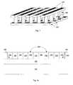
- FIG. 5is a circuit diagram illustrating an advantageous biasing scheme that may be used to set a selected cell formed according to the present invention without disturbing neighboring cells.
- FIG. 6is a circuit diagram illustrating an advantageous biasing scheme that may be used to reset a selected cell formed according to the present invention without disturbing neighboring cells.
- a variety of materialsshow reversible resistivity-switching behavior. These materials include chalcogenides, carbon polymers, perovskites, and certain metal oxides and nitrides. Specifically, there are metal oxide and nitride compounds which include only one metal and exhibit reliable resistivity-switching behavior. This group includes NiO, Nb 2 O 5 , TiO 2 , HfO 2 , Al 2 O 3 , CoO, MgO x , CrO 2 , VO, BN, and AlN.
- a layer of one of these materialsmay be formed in an initial state, for example a stable, relatively low-resistivity state. Upon application of sufficient voltage, the material switches to a stable high-resistivity state. (By applying different currents and voltages, more than two resistivity states may be achieved. For simplicity, this discussion will speak of high- and low-resistivity states, but it will be understood that more than two states are possible and may be useful.) This resistivity switching is reversible; subsequent application of appropriate current or voltage can serve to return the resistivity-switching material to a stable low-resistivity state.
- the set current(which switches the material from the high-resistivity state to the low-resistivity state) flows in one direction, while the reset current (which switches the material from the low-resistivity state to the high-resistivity state) must flow in the opposite direction.
- the direction of set and reset current flowis unimportant.
- the conversion from low-resistivity to high-resistivitycan be reversed, and the cycle can be repeated many times.
- the initial statemay be high-resistivity rather than low-resistivity.
- resistivity-switching material“resistivity-switching metal oxide or nitride”, “resistivity-switching memory element” or similar terms, it will be understood that a reversible resistivity-switching material is meant.
- the resistivity statemay store a data state of a memory cell; for example one resistivity state may correspond to a data “0”, for example, while the other resistivity state corresponds to a data “1”.
- one resistivity statemay correspond to a data “0”, for example, while the other resistivity state corresponds to a data “1”.
- more than two stable resistivity statesmay be achievable, allowing storage of more than two data states.
- resistivity switchingcan be reduced by introducing additional metal into a resistivity-switching metal oxide or nitride compound.
- resistivity switchingmay be achieved at the same set or reset voltage or current but in a shorter time.
- metals that are compatible with silicon processinginclude cobalt, aluminum, gallium, indium, nickel, niobium, zirconium, titanium, hafnium, tantalum, magnesium, chromium, vanadium, boron, yttrium, and lanthanum. Copper, iron, manganese, and zinc may have the desired properties, and may also be used, but are generally less compatible with silicon processing and are thus less preferred.
- the metal added to a metal oxide or nitride compoundcan either be the same as the metal of the compound, or different. Advantage may be gained either by adding extra nickel to a layer of NiO, for example, or by adding a different metal such as cobalt or aluminum to the NiO instead.
- the layer of resistivity-switching metal oxide or nitrideis a binary compound having two component elements, like NiO, a compound of nickel and oxygen, or AlN, a compound of aluminum and nitrogen.
- a binary compoundincludes exactly one metal.
- layeris formed in which the composition of the layer is predominantly one of these single-metal metal oxide or nitride compounds, and then extra atoms of another metal (or the same metal) are included in the layer. This is distinct from a layer formed of a more complex compound in which the compound itself has more than one metal; an example is a perovskite like CaTiO 3 .
- the added metalis a fairly small fraction of the completed resistivity-switching layer. Atoms of the added metal preferably are between about 0.01 and about 5 percent of the metal atoms present in the resistivity-switching layer.
- the resistivity-switching metal oxides or nitridescan be formed by methods including sputtering, chemical vapor deposition (CVD), a form of CVD known as atomic layer deposition (ALD), electrodeposition, and evaporation.
- the metal additivecan be introduced into the layer of the metal oxide or nitride compound by a variety of methods during or after formation of the layer. A few of the preferred methods to form a layer of a resistivity-switching oxide or nitride compound with a metal additive will be briefly described, but detailing all possible methods is impractical, and it will be understood by those skilled in the art that such resistivity-switching films with added metal formed by methods not specifically described here will still fall within the scope of the invention.
- the metal oxide or nitride layeris formed first by any conventional method, then is doped with the metal additive by ion implantation.
- a NiO filmcan be formed, then implanted with cobalt or aluminum ions.
- a small amount of the metal to be addedcan be provided by any appropriate method, such as ALD, above, below, adjacent to, or within the layer of metal oxide or nitride.
- ALDatomic layer deposition
- NiOMetal oxides and nitrides are often formed by reactive sputtering.
- a nickel sputtering targetis bombarded with a heavy inert ion such as argon and by O 2 .
- the nickel and oxygencombine, forming NiO.
- the metal to be addedis included in the sputtering target in the desired proportion.
- the metal to be addedis included in the sputtering target in the desired proportion.
- a NiO layeris to be formed with cobalt as the metal additive, in which about 95 percent of the metal atoms in the deposited layer are to be nickel atoms and about 5 percent are to be cobalt.
- An alloy target having sputter material that is 95 at % nickel and 5 at % cobaltwill provide these atoms in the desired proportion, and can be sputtered as usual by argon and O 2 .
- the atoms of the metal additivecan be between about 0.01 and about 5 percent of the metal atoms in the resistivity-switching metal oxide or nitride layer. If desired more than one metal additive can be included, though for simplicity this discussion will describe the use of one added metal.
- metal oxide or nitride compounds listedcan be deposited by CVD.
- some metal additivescan be added by in situ inclusion.
- a precursor gas or gasesare flowed under conditions that will cause the metal oxide or nitride to deposit on a substrate.
- An added metalis included in situ in a layer during CVD by simultaneously flowing a precursor gas which provides dopant atoms, in this case the metal additive, in the film as it forms. Suitable precursor gases are not available for all of the metal additives named, however.
- a precursor gas which provides dopant atomsin this case the metal additive, in the film as it forms.
- Suitable precursor gasesare not available for all of the metal additives named, however.
- the added metalis included in concentrations higher than those typical for a dopant; thus the process is here described as “in situ inclusion” rather than “in situ doping”.
- FIG. 1 ashows a resistivity-switching metal oxide or nitride layer 10 which includes a metal additive, while contact layers 14 and 16 , formed immediately below and above resistivity-switching layer 10 , are formed of the same metal oxide or nitride but with no metal additive.
- layer 10may be NiO with included aluminum or cobalt, while layers 14 and 16 are NiO with no added aluminum or cobalt, or in which aluminum or cobalt atoms are less than 0.01 percent of the metal atoms in these layers.
- contact layers 14 and 16will provide an improved electrical contact for resistivity-switching layer 10 , causing it to switch resistivity states at lower current or voltage than if contact layers 14 and 16 were not present. Contact layers 14 and 16 may or may not switch resistivity states as well.
- a compound stackmay include layers 14 , 10 , and 16 of the same resistivity-switching metal oxide or nitride in which resistivity-switching layer 10 does not include a metal additive and contact layers 14 and 16 do.
- the rail-shaped top and bottom conductorspreferably extend in different directions; for example they may be perpendicular.
- Disposed between the top conductor 400 and bottom conductor 200are a diode 30 and a resistance-switching element 118 arranged electrically in series.
- the resistance-switching element 118comprises a layer of resistivity-switching material which is converted from the low-resistance state to the high-resistance state, or, alternatively, from the high-resistance state to the low-resistance state, upon application of voltage across or flow of current through the resistance-switching element 118 .
- the conversion from low resistance to high resistanceis reversible.
- a material, such as nickel oxidehas a resistivity
- a discrete electrical elementsuch as a resistor, has a resistance.
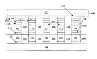
- FIG. 3shows a plurality of bottom conductors 200 and top conductors 400 , with intervening pillars 300 , the pillars 300 comprising diodes and resistance-switching elements.
- the diodecould be replaced with some other non-ohmic device.
- a first level of memory cellscan be formed; only a small portion of such a memory level is shown here.
- additional memory levelscan be formed stacked above this first memory level, forming a highly dense monolithic three dimensional memory array.
- the memory arrayis formed of deposited and grown layers above a substrate, for example a monocrystalline silicon substrate. Support circuitry is advantageously formed in the substrate below the memory array.
- Petti et al.U.S. patent application Ser. No. 11/143,269, “Rewriteable Memory Cell Comprising a Transistor and Resistance-Switching Material in Series,” filed Jun. 2, 2005 and hereby incorporated by reference, describes a memory cell having a layer of this resistivity-switching material formed in series with a MOS transistor.
- the MOS transistoris a thin-film transistor, having its channel region in deposited semiconductor material rather than in a monocrystalline wafer substrate.
- the resistivity-switching metal oxide or nitridecan have metal added according to the present invention to reduce set and reset voltages or currents or reduce switching time, and thus reduce overall power consumption.
- a state-change elementis an element that can attain a stable state which can reliably be sensed.
- a reversible state-change elementcan be reversibly switched between states.
- any state-change elementcomprising one of the named resistivity-switching metal oxides or nitrides is used to store a resistivity state, whether as a data state for a memory cell or for some other use
- that state-change elementmay benefit from the use of a metal additive to the metal oxide or nitride according to the present invention.
- a detailed examplewill be provided of fabrication of a monolithic three dimensional memory array formed according to a preferred embodiment of the present invention. For clarity many details, including steps, materials, and process conditions, will be included. It will be understood that this example is non-limiting, and that these details can be modified, omitted, or augmented while the results fall within the scope of the invention.
- the memory cell of Herner et al.U.S. patent application Ser. No. 10/955,549, “Nonvolatile Memory Cell Without a Dielectric Antifuse Having High- and Low-Impedance States,” filed Sep. 29, 2004, hereinafter the '549 application and hereby incorporated by reference, describes a memory cell including a diode formed of polycrystalline silicon (or polysilicon).
- the polysilicon of the diodeis formed in a high-resistivity state and can be converted to a low-resistivity state.
- the data state of the cellis effectively stored in the resistivity state of the polysilicon.
- deposited silicon crystallized with no adjacent layer of titanium silicidewill be relatively high in defects and high-resistivity as formed, while deposited silicon crystallized adjacent to a layer of titanium silicide will be lower in defects and low-resistivity as formed.
- High-defect, high-resistivity polysiliconcan have its order increased by programming, converting it to low-resistivity polysilicon; these two states can correspond to data states and can be the basis of a memory cell.
- Low-defect polysiliconis low-resistivity as formed, and thus cannot the basis of a memory cell using this mechanism.
- a memory cellwill pair a resistivity-switching metal oxide or nitride layer (having added metal) with a polysilicon diode.
- the resistivity-switching metal oxide or nitride layerwill store the data state; thus there is no need for the polysilicon of the diode to store this state as well, or for the large voltage required to convert it to a low-resistivity state.
- Herner et al., U.S. Pat. No. 6,952,030, “High-Density Three-Dimensional Memory Cell,”teaches a monolithic three dimensional memory array comprising memory cells, wherein each memory cell is a one-time programmable cell. The cell is formed in a high-resistance state, and, upon application of a programming voltage, is permanently converted to a low-resistance state.
- Related memory arraysare taught in Herner et al., U.S. patent application Ser. No. 11/015,824, “Nonvolatile Memory Cell Comprising a Reduced Height Vertical Diode,” filed Dec. 17, 2004; in Herner et al., U.S. patent application Ser. No.
- This substrate 100can be any semiconducting substrate as known in the art, such as monocrystalline silicon, IV-IV compounds like silicon-germanium or silicon-germanium-carbon, III-V compounds, II-VII compounds, epitaxial layers over such substrates, or any other semiconducting material.
- the substratemay include integrated circuits fabricated therein.
- the insulating layer 102is formed over substrate 100 .
- the insulating layer 102can be silicon oxide, silicon nitride, high-dielectric film, Si—C—O—H film, or any other suitable insulating material.
- the first conductors 200are formed over the substrate 100 and insulator 102 .
- An adhesion layer 104may be included between the insulating layer 102 and the conducting layer 106 to help the conducting layer 106 adhere.
- a preferred material for the adhesion layer 104is titanium nitride, though other materials may be used, or this layer may be omitted.
- Adhesion layer 104can be deposited by any conventional method, for example by sputtering.
- Conducting layer 106can comprise any conducting material known in the art, such as doped semiconductor, metals such as tungsten, or metal alloys or compounds.
- the layerswill be patterned and etched using any suitable masking and etching process to form substantially parallel, substantially coplanar conductors 200 , shown in FIG. 4 a in cross-section.
- photoresistis deposited, patterned by photolithography and the layers etched, and then the photoresist removed, using standard process techniques such as “ashing” in an oxygen-containing plasma, and strip of remaining polymers formed during etch in a conventional liquid solvent such as those formulated by EKC.
- Dielectric material 108can be any known electrically insulating material, such as silicon oxide, silicon nitride, or silicon oxynitride.
- silicon oxideis used as dielectric material 108 .
- the silicon oxidecan be deposited using any known process, such as chemical vapor deposition (CVD), or, for example, high-density plasma CVD (HDPCVD).
- planar surface 109is shown in FIG. 4 a.
- This removal of dielectric overfill to form planar surface 109can be performed by any process known in the art, such as etchback or chemical mechanical polishing (CMP).
- CMPchemical mechanical polishing
- the etchback techniques described in Raghuram et al., U.S. application Ser. No. 10/883417, “Nonselective Unpattemed Etchback to Expose Buried Patterned Features,” filed Jun. 30, 2004 and hereby incorporated by reference in its entirety,can advantageously be used.
- conductor railscan be formed by a Damascene process, in which oxide is deposited, trenches are etched in the oxide, then the trenches are filled with conductive material and overfill removed to create the conductor rails.
- a barrier layer 110is deposited as the first layer after planarization of the conductor rails. Any suitable material can be used in the barrier layer, including tungsten nitride, tantalum nitride, titanium nitride, or combinations of these materials. In a preferred embodiment, titanium nitride is used as the barrier layer. Where the barrier layer 110 is titanium nitride, it can be deposited in the same manner as the adhesion layer described earlier.
- semiconductor materialthat will be patterned into pillars is deposited. Any suitable semiconductor material or semiconductor alloy can be used. Silicon is preferred.
- junction diodeis used herein to refer to a semiconductor device with the property of non-ohmic conduction, having two terminal electrodes, and made of semiconducting material which is p-type at one electrode and n-type at the other.
- the semiconductor pillarcomprises a junction diode, the junction diode comprising a bottom heavily doped region of a first conductivity type and a top heavily doped region of a second conductivity type.
- the middle region, between the top and bottom regions,is an intrinsic or lightly doped region of either the first or second conductivity type.
- bottom heavily doped region 112is heavily doped n-type silicon.
- heavily doped region 112is deposited and doped with an n-type dopant such as phosphorus by any conventional method, preferably by in situ doping. This layer is preferably between about 200 and about 800 angstroms.
- top heavily doped p-type region 116will be formed by ion implantation.
- the thickness to be deposited in this stepwill be the final desired thickness of intrinsic region 114 plus the desired thickness of top heavily doped region 116 after implantation.
- intrinsic region 114is preferably between about 600 and about 2000 angstroms, for example about 1600 angstroms.
- Heavily doped p-type region 116is between about 100 and about 1000 angstroms, preferably about 400 angstroms.
- the thickness to be deposited undoped in this stepis between about 700 and about 3000 angstrom, preferably about 2000 angstroms.
- the diodes to be formedbe low-leakage p-i-n diodes. Leakage is minimized in such a diode by maximizing the thickness of the intrinsic region.
- Herner et al., U.S. patent application Ser. No. 11/215,951, “Ultrathin Chemically Grown Oxide Film as a Dopant Diffusion Barrier in Semiconductor Devices,” filed Aug. 31, 2005 and hereby incorporated by referencedescribes use of a chemically grown oxide between heavily doped region 112 and intrinsic region 114
- Kumar et al.U.S. patent application Ser. No. 11/271078, “Vertical Diode Doped With Antimony to Avoid or Limit Dopant Diffusion,” filed Nov.
- Top heavily doped regions 116are formed at this point by ion implantation with a p-type dopant, for example boron or BF 2 .
- a p-type dopantfor example boron or BF 2 .
- the diode described hereinhas a bottom n-type region and a top p-type region. If preferred, the conductivity types could be reversed.
- silicon regions 112 , 114 , and 116When deposited by conventional methods, silicon regions 112 , 114 , and 116 will be amorphous at this point, and will be crystallized in a later step. As described earlier and in the '530 application, if these layers are crystallized adjacent to a layer of a silicide, for example titanium silicide, the resulting polysilicon will be low in defects and relatively low-resistivity, providing a diode that will provide relatively high current without first requiring application of a large programming voltage.
- a silicidefor example titanium silicide
- the next layer depositedis layer 120 of titanium, which may be between about 30 and about 200 angstroms thick, preferably about 100 angstroms thick. Capping this is layer 122 of titanium nitride, which may be about 100 angstroms thick.
- an annealfor example a rapid thermal anneal will be performed. This anneal will cause titanium layer 120 to react with the silicon of layer 116 to form titanium silicide (not shown) and will crystallize silicon layers 112 , 114 , and 116 . During crystallization the silicon will be adjacent to a layer of titanium silicide, causing the resulting polysilicon to be low-resistivity.
- a layer 118 of a metal oxide or nitride resistivity-switching material including a metal additiveis formed on layer 120 .
- This layeris preferably between about 50 and about 600 angstroms, preferably about 400 angstroms.
- Layer 118can be any of the materials described earlier, and is preferably formed of a metal oxide or nitride compound having including exactly one metal which exhibits resistance switching behavior; preferably a material selected from the group consisting of NiO, Nb 2 O 5 , TiO 2 , HfO 2 , Al 2 O 3 , CoO, MgO x , CrO 2 , VO, BN, and AlN.
- the added metalis preferably cobalt, aluminum, gallium, indium, manganese, nickel, niobium, zirconium, titanium, hafnium, tantalum, magnesium, chromium, vanadium, boron, yttrium, or lanthanum.
- NiO layer 118 with added cobaltis formed by reactive sputtering, in which the sputtering target is at least 95 at % nickel and between 0.01 and 5 at % cobalt, for example between about 1 and about 2 at % cobalt.
- barrier layer 124is deposited on NiO layer 118 .
- Layer 124is preferably titanium nitride, though some other appropriate conductive barrier material may be used instead.
- An upcoming CMP stepwill be performed on layer 124 , so it is preferably relatively thick, about 800 angstroms.
- Pillars 300should have about the same pitch and about the same width as conductors 200 below, such that each pillar 300 is formed on top of a conductor 200 . Some misalignment can be tolerated.
- Pillars 300can be formed using any suitable masking and etching process.
- the stack to be etchedis relatively tall and includes materials which require the use of different etchants.
- photoresistis deposited, patterned using standard photolithography techniques, then titanium nitride layer 124 , NiO layer 118 , titanium nitride layer 122 , and titanium layer 120 are etched.
- An advantageous method to etch transition metal oxides, such as those of many preferred materials for resistivity-switching layer 118is described in Raghuram et al., U.S. patent application Ser. No. 11/179,423, “Method of Plasma Etching Transition Metals and Their Compounds,” filed Jul. 11, 2005 and hereby incorporated by reference. These etched layers can then act as a hard mask during etch of the remaining layers.
- Dielectric material 108is deposited over and between pillars 300 , filling the gaps between them.
- Dielectric material 108can be any known electrically insulating material, such as silicon oxide, silicon nitride, or silicon oxynitride.
- silicon dioxideis used as the insulating material.
- the silicon dioxidecan be deposited using any known process, such as CVD or HDPCVD.
- the dielectric material on top of the pillars 300is removed, exposing the tops of pillars 300 separated by dielectric material 108 , and leaving a substantially planar surface.
- This removal of dielectric overfill and planarizationcan be performed by any process known in the art, such as CMP or etchback.
- CMPchemical vapor deposition
- etchbackthe etchback techniques described in Raghuram et al. can be used.
- the resulting structureis shown in FIG. 4 b.
- layers 124 , 118 , 122 , and 120were patterned in a single patterning step with silicon regions 112 and 114 and 116 , followed by a multi-step etch. In some embodiments, however, it may be desirable to form the diode and the state-change element in separate patterning steps to reduce etch height and to avoid possible contamination by having NiO and metal barrier layers exposed in a chamber devoted to semiconductor etch.
- silicon regions 112 and 114are deposited, patterned and etched to form pillars. Dielectric fill is deposited to fill gaps between the pillars, and a CMP step removes overfill and exposes the tops of the pillars at a substantially planar surface.
- Top heavily doped regions 116are formed by ion implantation. Titanium layer 120 , titanium nitride layer 122 , NiO layer 118 , and titanium layer 124 are deposited on this planar surface, then patterned and etched in a separate step to form short pillars aligned with the diode pillars below. Some misalignment may be tolerated. Dielectric fill is deposited between the short pillars, and a CMP step removes overfill and exposes the tops of the pillars.
- barrier layer 122 , NiO layer 118 with added cobalt, and barrier layer 124can be formed before (and therefore beneath) diode layers 112 , 114 , and 116 , and may be patterned in the same or in a separate patterning step.
- the first layer of top conductors above the pillarswill be a titanium layer capped with titanium nitride. During a later anneal this titanium will react with the silicon at the top of the diode to form titanium silicide, providing a crystallization template to form a low-defect polycrystalline diode.
- contact layers of NiO with no added cobaltcould be formed directly above or below NiO layer 118 (which has added cobalt) to provide improved electrical contact for NiO layer 118 .
- top conductors 400After formation of pillars 300 is complete, a conductive material or stack is deposited to form the top conductors 400 .
- titanium nitride barrier layer 130is deposited next, followed by tungsten layer 132 .
- Top conductors 400can be patterned and etched as described earlier. In this example in each cell the diode (of layers 112 , 114 , and 116 ) and a state-change element (comprising resistance-switching layer 118 ) have been formed in series between top conductor 400 and bottom conductor 200 . Overlying second conductors 400 will preferably extend in a different direction from first conductors 200 , preferably substantially perpendicular to them.
- the resulting structure, shown in FIG. 4 cis a bottom or first level of memory cells.
- layers 121 , 118 , and 123will behave as a reversible state-change element.
- the reversible state-change elementis changed from a first resistance state to a second resistance state and back.
- the difference in resistance between the first resistance state and the second resistance statemay be at least a factor of five.
- Additional memory levelscan be formed above this first memory level.
- conductorscan be shared between memory levels; i.e. top conductor 400 would serve as the bottom conductor of the next memory level.
- an interlevel dielectricis formed above the first memory level of FIG. 4 c, its surface planarized, and construction of a second memory level begins on this planarized interlevel dielectric, with no shared conductors.
- a monolithic three dimensional memory arrayis one in which multiple memory levels are formed above a single substrate, such as a wafer, with no intervening substrates.
- the layers forming one memory levelare deposited or grown directly over the layers of an existing level or levels.
- stacked memorieshave been constructed by forming memory levels on separate substrates and adhering the memory levels atop each other, as in Leedy, U.S. Pat. No. 5,915,167, “Three dimensional structure memory.”
- the substratesmay be thinned or removed from the memory levels before bonding, but as the memory levels are initially formed over separate substrates, such memories are not true monolithic three dimensional memory arrays.
- a monolithic three dimensional memory array formed above a substratecomprises at least a first memory level formed at a first height above the substrate and a second memory level formed at a second height different from the first height. Three, four, eight, or indeed any number of memory levels can be formed above the substrate in such a multilevel array.
- resistivity-switching metal oxides or nitridesin some environments, require that the set current flows in one direction while the reset current flows in the opposite direction, while in others the direction of current flow is unimportant.
- the diodemust be biased in the forward direction to convert resistivity-switching layer 118 from the high-resistivity state to the low-resistivity state (a forward set current is required), while the diode must be biased in the reverse direction to convert resistivity-switching layer 118 from the low-resistivity state to the high-resistivity state (a reverse reset current is required.)
- interconnect line B 0is set to set voltage V SET
- interconnect line W 0is set to ground, applying V SET across selected cell S.
- unselected interconnect line B 1is set to ⁇ and interconnect line W 1 is set to V SET - ⁇ .
- V SETis 10 volts and ⁇ is 5 volts.
- a set voltage of 10 voltsis applied across selected cell S, causing it to switch.
- a forward voltage of 5 voltsis applied to both half-selected cells H (between interconnect line B 0 and interconnect line W 1 ) and F (between interconnect line B 1 and interconnect line W 0 ), a voltage too low to cause switching.
- no voltageis applied across unselected cell U.
- ⁇can be assigned within a range.
- the value for ⁇should be selected so that none of the H, F, or U cells is subjected to voltage or current large enough to cause set or reset.
- Unselected cell Uis subjected to a voltage of ⁇ -(V SET - ⁇ ), or 2 ⁇ -V SET .
- V SET - ⁇a voltage of ⁇ -(V SET - ⁇ )
- a reset voltageis applied, which, in this example, must be a negative voltage.
- Interconnect line B 0is set to reset voltage V RESET
- interconnect line W 0is set to ground, applying V RESET across selected cell S.
- unselected interconnect line B 1is set to ⁇ and unselected interconnect line W 1 is set to V RESET - ⁇ .
- V RESETvoltage RESET /2
- a reset voltage of ⁇ 10 voltsis applied across selected cell S, causing it to switch.
- a voltage of ⁇ 5 voltsis applied to both half-selected cells H (between interconnect line B 0 and interconnect line W 1 ) and F (between interconnect line B 1 and interconnect line W 0 ), a voltage too low to cause switching. No voltage is applied across unselected cell U.
- the value for ⁇can fall within a range, for example such that:
- set and reset voltages, and selected values for ⁇are examples for illustration only. Many values could be selected. It is routine to select optimal programming voltages and currents based on the characteristics of the memory cells.
Landscapes
- Engineering & Computer Science (AREA)
- Manufacturing & Machinery (AREA)
- Semiconductor Memories (AREA)
Abstract
Description
- The invention relates to a resistivity-switching material that can be used to store a data state in a nonvolatile memory cell.
- Resistivity-switching materials, which can reversibly be converted between higher and lower resistivity states, are known. Switching may be induced by subjecting the resistivity-switching material to a voltage or current, which may be relatively large. These two or more stable resistivity states make such materials an attractive option for use in a rewriteable non-volatile memory array. In a memory array based on such resistivity-switching material, it is generally advantageous to reduce power requirements.
- There is a need, therefore, to reduce the voltage, current, or switching time required to switch these resistivity-switching materials between stable resistivity states.
- The present invention is defined by the following claims, and nothing in this section should be taken as a limitation on those claims. In general, the invention is directed to resistivity-switching metal oxides or nitrides.
- A first aspect of the invention provides for a semiconductor device comprising: a reversible state-change element comprising a layer of a resistivity-switching metal oxide or nitride compound, the resistivity-switching metal oxide or nitride compound including only one metal, wherein the layer of resistivity-switching metal oxide or nitride compound includes a metal additive, wherein the metal additive is between about 0.01 and about 5 percent of the metal atoms in the layer of metal oxide or nitride compound.
- Another aspect of the invention provides for a rewriteable nonvolatile memory cell comprising: a state-change element comprising a layer of resistivity-switching metal oxide or nitride compound, the resistivity-switching metal oxide or nitride compound including only one metal, wherein the layer of resistivity-switching metal oxide or nitride compound includes a metal additive, wherein the metal additive is between about 0.01 and about 5 percent of the metal atoms in the layer of metal oxide or nitride compound, wherein a data state of the memory cell is stored in a resistivity state of the layer of resistivity-switching metal oxide or nitride compound.
- Yet another aspect of the invention provides for a method for forming a memory cell, the method comprising: forming a state-change element, the state-change element comprising a layer of resistivity-switching metal oxide or nitride compound, the resistivity-switching metal oxide or nitride compound including only one metal, wherein the layer of resistivity-switching metal oxide or nitride compound includes a metal additive, wherein the metal additive is between about 0.01 and about 5 percent of the metal atoms in the layer of metal oxide or nitride compound, wherein a data state of the memory cell corresponds to a resistivity state of the layer of resistivity-switching metal oxide or nitride compound.
- A preferred embodiment of the invention provides for a monolithic three dimensional memory array comprising: a) a first memory level formed above a substrate, the first memory level comprising: a plurality of first reversible state-change elements, each state-change element comprising a layer of a resistivity-switching metal oxide or nitride compound, the resistivity-switching metal oxide or nitride compound including only one metal, wherein the layer of resistivity-switching metal oxide or nitride compound includes a metal additive, wherein the metal additive is between about0.01 and about 5 percent of the metal atoms in the layer of metal oxide or nitride; and b) a second memory level monolithically formed above the first memory level.
- Another preferred embodiment provides for a method for forming a first memory level, the method comprising: forming a plurality of substantially parallel, substantially coplanar bottom conductors above a substrate; forming a plurality of substantially parallel, substantially coplanar top conductors above the bottom conductors; forming a plurality of vertically oriented diodes, each diode disposed between one of the bottom conductors and one of the top conductors; forming a plurality of reversible state-change elements, each state-change element comprising a layer of a resistivity-switching metal oxide or nitride compound, the resistivity-switching metal oxide or nitride compound including only one metal, wherein the layer of resistivity-switching metal oxide or nitride compound includes a metal additive, wherein the metal additive is between about 0.01 and about 5 percent of the metal atoms in the layer of metal oxide or nitride compound, wherein each state-change element is disposed between one of the diodes and one of the top conductors or between one of the diodes and one of the bottom conductors.
- Another aspect of the invention provides for a method for forming a nonvolatile memory cell comprising a reversible state-change element, the method comprising: forming a layer of a resistivity-switching metal oxide or nitride compound, the resistivity-switching metal oxide or nitride compound including only one metal, which is a first metal; and during or after the step of forming the layer of a resistivity-switching metal oxide or nitride compound, adding a second metal to the layer of resistivity-switching metal oxide or nitride compound, wherein the reversible state-change element comprises the layer of resistivity-switching metal oxide or nitride compound.
- A preferred embodiment of the invention provides for a nonvolatile memory cell comprising: a state-change element comprising: a) a bottom contact layer consisting essentially of a first metal oxide or metal nitride compound, the first metal oxide or metal nitride compound including only one metal; b) a resistivity-switching layer consisting essentially of the first metal oxide or metal nitride compound and a metal additive, wherein the metal additive is between about 0.01 and about 5 percent of the metal atoms in the resistivity-switching layer; and c) a top contact layer consisting essentially of the first metal oxide or metal nitride compound, wherein the resistivity-switching layer is above and in contact with the bottom contact layer and the top contact layer is above and in contact with the resistivity-switching layer, wherein a data state of the memory cell is stored in a resistance state of the state-change element.
- A related embodiment provides for a nonvolatile memory cell comprising: a state-change element comprising: a) a bottom contact layer consisting essentially of a first metal oxide or metal nitride compound and a metal additive, wherein the metal additive is between about 0.01 and about 5 percent of the metal atoms in the bottom contact layer and wherein the first metal oxide or metal nitride compound includes only one metal; b) a resistivity-switching layer consisting essentially of the first metal oxide or metal nitride compound; and c) a top contact layer consisting essentially of the first metal oxide or metal nitride compound and the metal additive, wherein the metal additive is between about 0.01 and about 5 percent of the metal atoms in the top contact layer, wherein the resistivity-switching layer is above and in contact with the bottom contact layer and the top contact layer is above and in contact with the resistivity-switching layer, wherein a data state of the memory cell is stored in a resistance state of the state-change element.
- Each of the aspects and embodiments of the invention described herein can be used alone or in combination with one another.
- The preferred aspects and embodiments will now be described with reference to the attached drawings.
FIGS. 1 aand1bare cross-sectional views of compound stacks of a resistivity-switching layers and contact layers, the layers of metal oxide or nitride, one or more formed with and one or more formed without added metal, according to an embodiment of the present invention.FIG. 2 is a perspective view of a nonvolatile memory cell including a diode and a resistance-switching element disposed in series between a top and a bottom conductor which may advantageously be modified to use aspects of the present invention.FIG. 3 is a perspective view of a portion of a memory level of memory cells like those ofFIG. 2 .FIGS. 4 a-4care cross-sectional views illustrating stages in fabrication of a memory level of nonvolatile memory cells formed according to an embodiment of the present invention.FIG. 5 is a circuit diagram illustrating an advantageous biasing scheme that may be used to set a selected cell formed according to the present invention without disturbing neighboring cells.FIG. 6 is a circuit diagram illustrating an advantageous biasing scheme that may be used to reset a selected cell formed according to the present invention without disturbing neighboring cells.- A variety of materials show reversible resistivity-switching behavior. These materials include chalcogenides, carbon polymers, perovskites, and certain metal oxides and nitrides. Specifically, there are metal oxide and nitride compounds which include only one metal and exhibit reliable resistivity-switching behavior. This group includes NiO, Nb2O5, TiO2, HfO2, Al2O3, CoO, MgOx, CrO2, VO, BN, and AlN.
- A layer of one of these materials may be formed in an initial state, for example a stable, relatively low-resistivity state. Upon application of sufficient voltage, the material switches to a stable high-resistivity state. (By applying different currents and voltages, more than two resistivity states may be achieved. For simplicity, this discussion will speak of high- and low-resistivity states, but it will be understood that more than two states are possible and may be useful.) This resistivity switching is reversible; subsequent application of appropriate current or voltage can serve to return the resistivity-switching material to a stable low-resistivity state. For some of these resistivity-switching materials, and in some environments, the set current (which switches the material from the high-resistivity state to the low-resistivity state) flows in one direction, while the reset current (which switches the material from the low-resistivity state to the high-resistivity state) must flow in the opposite direction. For other resistivity-switching materials, in other environments, the direction of set and reset current flow is unimportant.
- The conversion from low-resistivity to high-resistivity can be reversed, and the cycle can be repeated many times. Depending on the material and the environment, the initial state may be high-resistivity rather than low-resistivity. When this discussion refers to “resistivity-switching material”, “resistivity-switching metal oxide or nitride”, “resistivity-switching memory element” or similar terms, it will be understood that a reversible resistivity-switching material is meant.
- This resistivity-switching behavior makes these materials of interest for use in nonvolatile memory arrays. The resistivity state may store a data state of a memory cell; for example one resistivity state may correspond to a data “0”, for example, while the other resistivity state corresponds to a data “1”. As noted, in some materials more than two stable resistivity states may be achievable, allowing storage of more than two data states.
- The actual conversion mechanism is not well-understood. Set and reset voltages are applied, but it is unclear if it is the applied voltage or current flow that actually causes the switch. In general set and reset voltages and currents must be relatively large. The resistivity state is sensed by applying a read voltage, which is smaller than either the set or reset voltage. For a given read voltage, current flow will be higher when the resistivity-switching material is in the low-resistivity state than when it is in the high-resistivity state.
- In electronic devices it is frequently advantageous to reduce power requirements. In a memory array using resistivity-switching metal oxides or nitrides, power requirements are reduced by decreasing the set and reset voltages and currents.
- It has been found that the set and reset voltages or currents that must be applied to induce resistivity switching can be reduced by introducing additional metal into a resistivity-switching metal oxide or nitride compound. Alternatively, resistivity switching may be achieved at the same set or reset voltage or current but in a shorter time.
- It is most practical to use metals that are compatible with silicon processing; thus preferred metals to use as this additive include cobalt, aluminum, gallium, indium, nickel, niobium, zirconium, titanium, hafnium, tantalum, magnesium, chromium, vanadium, boron, yttrium, and lanthanum. Copper, iron, manganese, and zinc may have the desired properties, and may also be used, but are generally less compatible with silicon processing and are thus less preferred. The metal added to a metal oxide or nitride compound can either be the same as the metal of the compound, or different. Advantage may be gained either by adding extra nickel to a layer of NiO, for example, or by adding a different metal such as cobalt or aluminum to the NiO instead.
- Note that the layer of resistivity-switching metal oxide or nitride is a binary compound having two component elements, like NiO, a compound of nickel and oxygen, or AlN, a compound of aluminum and nitrogen. Such a binary compound includes exactly one metal. In the present invention layer is formed in which the composition of the layer is predominantly one of these single-metal metal oxide or nitride compounds, and then extra atoms of another metal (or the same metal) are included in the layer. This is distinct from a layer formed of a more complex compound in which the compound itself has more than one metal; an example is a perovskite like CaTiO3.
- This discussion will speak of an oxide or nitride layer having an added metal or a metal additive. Other terms are commonly used to describe addition of a metal to a material. When a metal such as boron is added to silicon to enhance its conductivity, for example, the added boron is generally described as a dopant. A dopant normally appears in very low concentration; a typical dopant concentration is about 1019dopant atoms/cm3. A metal may also be added to another metal to form an alloy, in which two (or more) metals are combined in any ratio. To avoid any expectations of concentration that might come with the use of such terms, this discussion will opt for the more neutral terms “added metal” and “metal additive”. In aspects of the invention, the added metal is a fairly small fraction of the completed resistivity-switching layer. Atoms of the added metal preferably are between about 0.01 and about 5 percent of the metal atoms present in the resistivity-switching layer.
- The resistivity-switching metal oxides or nitrides can be formed by methods including sputtering, chemical vapor deposition (CVD), a form of CVD known as atomic layer deposition (ALD), electrodeposition, and evaporation. The metal additive can be introduced into the layer of the metal oxide or nitride compound by a variety of methods during or after formation of the layer. A few of the preferred methods to form a layer of a resistivity-switching oxide or nitride compound with a metal additive will be briefly described, but detailing all possible methods is impractical, and it will be understood by those skilled in the art that such resistivity-switching films with added metal formed by methods not specifically described here will still fall within the scope of the invention.
- In some embodiments, the metal oxide or nitride layer is formed first by any conventional method, then is doped with the metal additive by ion implantation. For example, a NiO film can be formed, then implanted with cobalt or aluminum ions.
- Alternatively, a small amount of the metal to be added can be provided by any appropriate method, such as ALD, above, below, adjacent to, or within the layer of metal oxide or nitride. The provided metal additive will then diffuse through the metal oxide or nitride layer.
- Metal oxides and nitrides are often formed by reactive sputtering. To form NiO by this method, a nickel sputtering target is bombarded with a heavy inert ion such as argon and by O2. The nickel and oxygen combine, forming NiO.
- To form a metal oxide or nitride with a metal additive by sputtering, the metal to be added is included in the sputtering target in the desired proportion. For example, suppose a NiO layer is to be formed with cobalt as the metal additive, in which about 95 percent of the metal atoms in the deposited layer are to be nickel atoms and about 5 percent are to be cobalt. An alloy target having sputter material that is 95 at % nickel and 5 at % cobalt will provide these atoms in the desired proportion, and can be sputtered as usual by argon and O2. In various embodiments the atoms of the metal additive can be between about 0.01 and about 5 percent of the metal atoms in the resistivity-switching metal oxide or nitride layer. If desired more than one metal additive can be included, though for simplicity this discussion will describe the use of one added metal.
- Some of the metal oxide or nitride compounds listed can be deposited by CVD. In these cases some metal additives can be added by in situ inclusion. During CVD a precursor gas or gases are flowed under conditions that will cause the metal oxide or nitride to deposit on a substrate. An added metal is included in situ in a layer during CVD by simultaneously flowing a precursor gas which provides dopant atoms, in this case the metal additive, in the film as it forms. Suitable precursor gases are not available for all of the metal additives named, however. (It is known to add a conductivity-enhancing dopant to deposited silicon by in situ doping. As described, in aspects of the present invention the added metal is included in concentrations higher than those typical for a dopant; thus the process is here described as “in situ inclusion” rather than “in situ doping”.)
- It may also be desirable to form the resistivity-switching metal oxide or nitride layer in a compound stack with variable composition.
FIG. 1 ashows a resistivity-switching metal oxide ornitride layer 10 which includes a metal additive, while contact layers14 and16, formed immediately below and above resistivity-switching layer 10, are formed of the same metal oxide or nitride but with no metal additive. For example,layer 10 may be NiO with included aluminum or cobalt, whilelayers switching layer 10, causing it to switch resistivity states at lower current or voltage than if contact layers14 and16 were not present. Contact layers14 and16 may or may not switch resistivity states as well. - In an alternative embodiment shown in
FIG. 1 b,a compound stack may includelayers switching layer 10 does not include a metal additive andcontact layers - In Herner et al., U.S. patent application Ser. No. 11/125,939, “Rewriteable Memory Cell Comprising a Diode and a Resistance-Switching Material,” filed May 9, 2005, hereinafter the '939 application and hereby incorporated by reference, a diode is paired with a resistivity-switching material to form a rewriteable nonvolatile memory cell that can be formed and programmed in a large, high-density array. An embodiment of the '939 application is shown in
FIG. 2 . The cell includes a portion of abottom conductor 200 and a portion of atop conductor 400. The rail-shaped top and bottom conductors preferably extend in different directions; for example they may be perpendicular. Disposed between thetop conductor 400 andbottom conductor 200 are adiode 30 and a resistance-switchingelement 118 arranged electrically in series. The resistance-switchingelement 118 comprises a layer of resistivity-switching material which is converted from the low-resistance state to the high-resistance state, or, alternatively, from the high-resistance state to the low-resistance state, upon application of voltage across or flow of current through the resistance-switchingelement 118. The conversion from low resistance to high resistance is reversible. (Note that this discussion speaks of both resistivity and resistance states. A material, such as nickel oxide, has a resistivity, while a discrete electrical element, such as a resistor, has a resistance.) FIG. 3 shows a plurality ofbottom conductors 200 andtop conductors 400, with interveningpillars 300, thepillars 300 comprising diodes and resistance-switching elements. In an alternative embodiment, the diode could be replaced with some other non-ohmic device. In this way a first level of memory cells can be formed; only a small portion of such a memory level is shown here. In preferred embodiments, additional memory levels can be formed stacked above this first memory level, forming a highly dense monolithic three dimensional memory array. The memory array is formed of deposited and grown layers above a substrate, for example a monocrystalline silicon substrate. Support circuitry is advantageously formed in the substrate below the memory array.- Petti et al., U.S. patent application Ser. No. 11/143,269, “Rewriteable Memory Cell Comprising a Transistor and Resistance-Switching Material in Series,” filed Jun. 2, 2005 and hereby incorporated by reference, describes a memory cell having a layer of this resistivity-switching material formed in series with a MOS transistor. In embodiments of Petti et al., the MOS transistor is a thin-film transistor, having its channel region in deposited semiconductor material rather than in a monocrystalline wafer substrate.
- In either the '939 application or Petti et al., the resistivity-switching metal oxide or nitride can have metal added according to the present invention to reduce set and reset voltages or currents or reduce switching time, and thus reduce overall power consumption. A state-change element is an element that can attain a stable state which can reliably be sensed. A reversible state-change element can be reversibly switched between states. More generally, then, in any memory or any device in which a state-change element comprising one of the named resistivity-switching metal oxides or nitrides is used to store a resistivity state, whether as a data state for a memory cell or for some other use, that state-change element may benefit from the use of a metal additive to the metal oxide or nitride according to the present invention.
- A detailed example will be provided of fabrication of a monolithic three dimensional memory array formed according to a preferred embodiment of the present invention. For clarity many details, including steps, materials, and process conditions, will be included. It will be understood that this example is non-limiting, and that these details can be modified, omitted, or augmented while the results fall within the scope of the invention.
- The memory cell of Herner et al., U.S. patent application Ser. No. 10/955,549, “Nonvolatile Memory Cell Without a Dielectric Antifuse Having High- and Low-Impedance States,” filed Sep. 29, 2004, hereinafter the '549 application and hereby incorporated by reference, describes a memory cell including a diode formed of polycrystalline silicon (or polysilicon). The polysilicon of the diode is formed in a high-resistivity state and can be converted to a low-resistivity state. The data state of the cell is effectively stored in the resistivity state of the polysilicon.
- As described in Herner et al., U.S. patent application Ser. No. 11/148,530, “Nonvolatile Memory Cell Operating by Increasing Order in Polycrystalline Semiconductor Material,” filed Jun. 8, 2005, hereinafter the '530 application and hereby incorporated by reference, it is believed that when amorphous silicon is crystallized adjacent to certain silicides, the resulting polysilicon may be more highly ordered and thus more conductive than silicon crystallized with no adjacent silicide. It is believed that an adjacent layer of, for example, titanium silicide may have a lattice spacing and orientation which will provide a crystallization template for the silicon as it crystallizes, allowing it to crystallize with relatively few defects. In short, deposited silicon crystallized with no adjacent layer of titanium silicide will be relatively high in defects and high-resistivity as formed, while deposited silicon crystallized adjacent to a layer of titanium silicide will be lower in defects and low-resistivity as formed. High-defect, high-resistivity polysilicon can have its order increased by programming, converting it to low-resistivity polysilicon; these two states can correspond to data states and can be the basis of a memory cell. Low-defect polysilicon is low-resistivity as formed, and thus cannot the basis of a memory cell using this mechanism.
- In the memory to be described, a memory cell will pair a resistivity-switching metal oxide or nitride layer (having added metal) with a polysilicon diode. The resistivity-switching metal oxide or nitride layer will store the data state; thus there is no need for the polysilicon of the diode to store this state as well, or for the large voltage required to convert it to a low-resistivity state. In the memory to be described, then, it may be preferred that the polysilicon of the polysilicon diode be formed in a low-resistivity state, with an adjacent silicide.
- Herner et al., U.S. Pat. No. 6,952,030, “High-Density Three-Dimensional Memory Cell,” teaches a monolithic three dimensional memory array comprising memory cells, wherein each memory cell is a one-time programmable cell. The cell is formed in a high-resistance state, and, upon application of a programming voltage, is permanently converted to a low-resistance state. Related memory arrays are taught in Herner et al., U.S. patent application Ser. No. 11/015,824, “Nonvolatile Memory Cell Comprising a Reduced Height Vertical Diode,” filed Dec. 17, 2004; in Herner et al., U.S. patent application Ser. No. 11/125,606, “High-Density Nonvolatile Memory Array Fabricated at Low Temperature Comprising Semiconductor Diodes,” filed May 9, 2005; and in Herner et al., U.S. patent application Ser. No. 10/954,577, “Junction Diode Comprising Varying Semiconductor Compositions,” filed Sep. 29, 2004, all hereby incorporated by reference. Teachings of the '939 application, of Petti et al., and of the other incorporated applications and patents will be useful in formation of a memory array according to the present invention. To avoid obscuring the invention, not all of the details of the incorporated applications and patents will be included, but it will be understood that no teaching of these applications or patents is intended to be excluded.
- Turning to
FIG. 4 a,formation of the memory begins with asubstrate 100. Thissubstrate 100 can be any semiconducting substrate as known in the art, such as monocrystalline silicon, IV-IV compounds like silicon-germanium or silicon-germanium-carbon, III-V compounds, II-VII compounds, epitaxial layers over such substrates, or any other semiconducting material. The substrate may include integrated circuits fabricated therein. - An insulating
layer 102 is formed oversubstrate 100. The insulatinglayer 102 can be silicon oxide, silicon nitride, high-dielectric film, Si—C—O—H film, or any other suitable insulating material. - The
first conductors 200 are formed over thesubstrate 100 andinsulator 102. Anadhesion layer 104 may be included between the insulatinglayer 102 and theconducting layer 106 to help theconducting layer 106 adhere. A preferred material for theadhesion layer 104 is titanium nitride, though other materials may be used, or this layer may be omitted.Adhesion layer 104 can be deposited by any conventional method, for example by sputtering. - The next layer to be deposited is conducting
layer 106. Conductinglayer 106 can comprise any conducting material known in the art, such as doped semiconductor, metals such as tungsten, or metal alloys or compounds. - Once all the layers that will form the conductor rails have been deposited, the layers will be patterned and etched using any suitable masking and etching process to form substantially parallel, substantially
coplanar conductors 200, shown inFIG. 4 ain cross-section. In one embodiment, photoresist is deposited, patterned by photolithography and the layers etched, and then the photoresist removed, using standard process techniques such as “ashing” in an oxygen-containing plasma, and strip of remaining polymers formed during etch in a conventional liquid solvent such as those formulated by EKC. - Next a
dielectric material 108 is deposited over and between conductor rails200.Dielectric material 108 can be any known electrically insulating material, such as silicon oxide, silicon nitride, or silicon oxynitride. In a preferred embodiment, silicon oxide is used asdielectric material 108. The silicon oxide can be deposited using any known process, such as chemical vapor deposition (CVD), or, for example, high-density plasma CVD (HDPCVD). - Finally, excess
dielectric material 108 on top ofconductor rails 200 is removed, exposing the tops ofconductor rails 200 separated bydielectric material 108, and leaving a substantiallyplanar surface 109. The resulting structure is shown inFIG. 4 a.This removal of dielectric overfill to formplanar surface 109 can be performed by any process known in the art, such as etchback or chemical mechanical polishing (CMP). For example, the etchback techniques described in Raghuram et al., U.S. application Ser. No. 10/883417, “Nonselective Unpattemed Etchback to Expose Buried Patterned Features,” filed Jun. 30, 2004 and hereby incorporated by reference in its entirety, can advantageously be used. Alternatively, conductor rails can be formed by a Damascene process, in which oxide is deposited, trenches are etched in the oxide, then the trenches are filled with conductive material and overfill removed to create the conductor rails. - Next, turning to
FIG. 4 b,vertical pillars will be formed above completed conductor rails200. (To savespace substrate 100 is omitted inFIG. 4 band subsequent figures; its presence will be assumed.) Preferably abarrier layer 110 is deposited as the first layer after planarization of the conductor rails. Any suitable material can be used in the barrier layer, including tungsten nitride, tantalum nitride, titanium nitride, or combinations of these materials. In a preferred embodiment, titanium nitride is used as the barrier layer. Where thebarrier layer 110 is titanium nitride, it can be deposited in the same manner as the adhesion layer described earlier. - Next semiconductor material that will be patterned into pillars is deposited. Any suitable semiconductor material or semiconductor alloy can be used. Silicon is preferred.
- The term junction diode is used herein to refer to a semiconductor device with the property of non-ohmic conduction, having two terminal electrodes, and made of semiconducting material which is p-type at one electrode and n-type at the other. In preferred embodiments, the semiconductor pillar comprises a junction diode, the junction diode comprising a bottom heavily doped region of a first conductivity type and a top heavily doped region of a second conductivity type. The middle region, between the top and bottom regions, is an intrinsic or lightly doped region of either the first or second conductivity type.
- In this example, bottom heavily doped
region 112 is heavily doped n-type silicon. In a most preferred embodiment, heavily dopedregion 112 is deposited and doped with an n-type dopant such as phosphorus by any conventional method, preferably by in situ doping. This layer is preferably between about 200 and about 800 angstroms. - Next the silicon that will form the remainder of the diode is deposited by any method known in the art. In a preferred embodiment top heavily doped p-
type region 116 will be formed by ion implantation. The thickness to be deposited in this step, then, will be the final desired thickness ofintrinsic region 114 plus the desired thickness of top heavily dopedregion 116 after implantation. In the finished device,intrinsic region 114 is preferably between about 600 and about 2000 angstroms, for example about 1600 angstroms. Heavily doped p-type region 116 is between about 100 and about 1000 angstroms, preferably about 400 angstroms. (Some thickness, for example about 200 angstroms, oflayer 116 will be consumed during silicide formation in a later step; thus the thickness oflayer 116 may be selected to allow for this anticipated loss.) The thickness to be deposited undoped in this step, then, is between about 700 and about 3000 angstrom, preferably about 2000 angstroms. - It is preferred that the diodes to be formed be low-leakage p-i-n diodes. Leakage is minimized in such a diode by maximizing the thickness of the intrinsic region. Herner et al., U.S. patent application Ser. No. 11/215,951, “Ultrathin Chemically Grown Oxide Film as a Dopant Diffusion Barrier in Semiconductor Devices,” filed Aug. 31, 2005 and hereby incorporated by reference, describes use of a chemically grown oxide between heavily doped
region 112 andintrinsic region 114, while Kumar et al., U.S. patent application Ser. No. 11/271078, “Vertical Diode Doped With Antimony to Avoid or Limit Dopant Diffusion,” filed Nov. 10, 2005, owned by the assignee of the present invention and hereby incorporated by reference, describes doping heavily dopedregion 112 with antimony; both methods serve to prevent or limit diffusion of dopant from heavily dopedregion 112 intointrinsic region 114. Diffusion of dopant into the intrinsic region decreases its thickness and increases leakage; thus these methods to limit dopant diffusion may advantageously be used in embodiments of the present invention to form a low-leakage diode. - Top heavily doped
regions 116 are formed at this point by ion implantation with a p-type dopant, for example boron or BF2. The diode described herein has a bottom n-type region and a top p-type region. If preferred, the conductivity types could be reversed. - When deposited by conventional methods,
silicon regions - In preferred embodiments, the next layer deposited is
layer 120 of titanium, which may be between about 30 and about 200 angstroms thick, preferably about 100 angstroms thick. Capping this islayer 122 of titanium nitride, which may be about 100 angstroms thick. In a later step an anneal, for example a rapid thermal anneal will be performed. This anneal will causetitanium layer 120 to react with the silicon oflayer 116 to form titanium silicide (not shown) and will crystallizesilicon layers - A
layer 118 of a metal oxide or nitride resistivity-switching material including a metal additive is formed onlayer 120. This layer is preferably between about 50 and about 600 angstroms, preferably about 400 angstroms.Layer 118 can be any of the materials described earlier, and is preferably formed of a metal oxide or nitride compound having including exactly one metal which exhibits resistance switching behavior; preferably a material selected from the group consisting of NiO, Nb2O5, TiO2, HfO2, Al2O3, CoO, MgOx, CrO2, VO, BN, and AlN. The added metal is preferably cobalt, aluminum, gallium, indium, manganese, nickel, niobium, zirconium, titanium, hafnium, tantalum, magnesium, chromium, vanadium, boron, yttrium, or lanthanum. For simplicity this discussion will describe the use of NiO with added cobalt inlayer 118, though it will be understood that other materials may be used. In preferredembodiments NiO layer 118 with added cobalt is formed by reactive sputtering, in which the sputtering target is at least 95 at % nickel and between 0.01 and 5 at % cobalt, for example between about 1 and about 2 at % cobalt. - Finally in preferred
embodiments barrier layer 124 is deposited onNiO layer 118.Layer 124 is preferably titanium nitride, though some other appropriate conductive barrier material may be used instead. An upcoming CMP step will be performed onlayer 124, so it is preferably relatively thick, about 800 angstroms. - Returning to
FIG. 4 b,at this stage layers124,118,122, and120, which will make up the resistance-switching state-change element, andsilicon regions pillars 300.Pillars 300 should have about the same pitch and about the same width asconductors 200 below, such that eachpillar 300 is formed on top of aconductor 200. Some misalignment can be tolerated. Pillars 300 can be formed using any suitable masking and etching process. The stack to be etched is relatively tall and includes materials which require the use of different etchants. Preferably, then, photoresist is deposited, patterned using standard photolithography techniques, thentitanium nitride layer 124,NiO layer 118,titanium nitride layer 122, andtitanium layer 120 are etched. An advantageous method to etch transition metal oxides, such as those of many preferred materials for resistivity-switching layer 118, is described in Raghuram et al., U.S. patent application Ser. No. 11/179,423, “Method of Plasma Etching Transition Metals and Their Compounds,” filed Jul. 11, 2005 and hereby incorporated by reference. These etched layers can then act as a hard mask during etch of the remaining layers.- The photolithography techniques described in Chen, U.S. application Ser. No. 10/728,436, “Photomask Features with Interior Nonprinting Window Using Alternating Phase Shifting,” filed Dec. 5, 2003; or Chen, U.S. application Ser. No. 10/815,312, Photomask Features with Chromeless Nonprinting Phase Shifting Window,” filed Apr. 1, 2004, both owned by the assignee of the present invention and hereby incorporated by reference, can advantageously be used to perform any photolithography step used in formation of a memory array according to the present invention.
Dielectric material 108 is deposited over and betweenpillars 300, filling the gaps between them.Dielectric material 108 can be any known electrically insulating material, such as silicon oxide, silicon nitride, or silicon oxynitride. In a preferred embodiment, silicon dioxide is used as the insulating material. The silicon dioxide can be deposited using any known process, such as CVD or HDPCVD.- Next the dielectric material on top of the
pillars 300 is removed, exposing the tops ofpillars 300 separated bydielectric material 108, and leaving a substantially planar surface. This removal of dielectric overfill and planarization can be performed by any process known in the art, such as CMP or etchback. For example, the etchback techniques described in Raghuram et al. can be used. The resulting structure is shown inFIG. 4 b. - In this example, layers124,118,122, and120 were patterned in a single patterning step with
silicon regions silicon regions regions 116 are formed by ion implantation.Titanium layer 120,titanium nitride layer 122,NiO layer 118, andtitanium layer 124 are deposited on this planar surface, then patterned and etched in a separate step to form short pillars aligned with the diode pillars below. Some misalignment may be tolerated. Dielectric fill is deposited between the short pillars, and a CMP step removes overfill and exposes the tops of the pillars. - In other alternative embodiments,
barrier layer 122,NiO layer 118 with added cobalt, andbarrier layer 124 can be formed before (and therefore beneath) diode layers112,114, and116, and may be patterned in the same or in a separate patterning step. In this case, the first layer of top conductors above the pillars will be a titanium layer capped with titanium nitride. During a later anneal this titanium will react with the silicon at the top of the diode to form titanium silicide, providing a crystallization template to form a low-defect polycrystalline diode. - In still other embodiments, contact layers of NiO with no added cobalt could be formed directly above or below NiO layer118 (which has added cobalt) to provide improved electrical contact for
NiO layer 118. - Turning to
FIG. 4 c,after formation ofpillars 300 is complete, a conductive material or stack is deposited to form thetop conductors 400. In a preferred embodiment, titaniumnitride barrier layer 130 is deposited next, followed bytungsten layer 132.Top conductors 400 can be patterned and etched as described earlier. In this example in each cell the diode (oflayers top conductor 400 andbottom conductor 200. Overlyingsecond conductors 400 will preferably extend in a different direction fromfirst conductors 200, preferably substantially perpendicular to them. The resulting structure, shown inFIG. 4 c,is a bottom or first level of memory cells. - In each memory cell in this memory level, layers121,118, and123, and contact layers if they are included, will behave as a reversible state-change element. During normal operation of the device, the reversible state-change element is changed from a first resistance state to a second resistance state and back. The difference in resistance between the first resistance state and the second resistance state may be at least a factor of five.
- Additional memory levels can be formed above this first memory level. In some embodiments, conductors can be shared between memory levels; i.e.
top conductor 400 would serve as the bottom conductor of the next memory level. In other embodiments, an interlevel dielectric is formed above the first memory level ofFIG. 4 c,its surface planarized, and construction of a second memory level begins on this planarized interlevel dielectric, with no shared conductors. - A monolithic three dimensional memory array is one in which multiple memory levels are formed above a single substrate, such as a wafer, with no intervening substrates. The layers forming one memory level are deposited or grown directly over the layers of an existing level or levels. In contrast, stacked memories have been constructed by forming memory levels on separate substrates and adhering the memory levels atop each other, as in Leedy, U.S. Pat. No. 5,915,167, “Three dimensional structure memory.” The substrates may be thinned or removed from the memory levels before bonding, but as the memory levels are initially formed over separate substrates, such memories are not true monolithic three dimensional memory arrays.
- A monolithic three dimensional memory array formed above a substrate comprises at least a first memory level formed at a first height above the substrate and a second memory level formed at a second height different from the first height. Three, four, eight, or indeed any number of memory levels can be formed above the substrate in such a multilevel array.
- Biasing of Array Lines for Set and Reset
- As noted, some of the resistivity-switching metal oxides or nitrides, in some environments, require that the set current flows in one direction while the reset current flows in the opposite direction, while in others the direction of current flow is unimportant.
- Suppose, in a memory array like that of
FIG. 4 c,the diode must be biased in the forward direction to convert resistivity-switching layer 118 from the high-resistivity state to the low-resistivity state (a forward set current is required), while the diode must be biased in the reverse direction to convert resistivity-switching layer 118 from the low-resistivity state to the high-resistivity state (a reverse reset current is required.) - A cell must be put in the low-resistivity state without inadvertently switching neighboring cells which share top or bottom conductors. Turning to
FIG. 5 , to switch selected cell S from the high-resistance state to the low-resistance state, interconnect line B0is set to set voltage VSET, and interconnect line W0is set to ground, applying VSETacross selected cell S. To avoid switching other cells in the array, unselected interconnect line B1is set to Δ and interconnect line W1is set to VSET-Δ. - For example, suppose VSETis 10 volts and Δ is 5 volts. A set voltage of 10 volts is applied across selected cell S, causing it to switch. A forward voltage of 5 volts is applied to both half-selected cells H (between interconnect line B0and interconnect line W1) and F (between interconnect line B1and interconnect line W0), a voltage too low to cause switching. For the VSETand Δ values selected, no voltage is applied across unselected cell U.
- Clearly the value for Δ can be assigned within a range. The value for Δ should be selected so that none of the H, F, or U cells is subjected to voltage or current large enough to cause set or reset. Unselected cell U is subjected to a voltage of Δ-(VSET-Δ), or 2Δ-VSET. In general, then, to avoid unintentional reset of unselected cell U:
|2Δ-VSET|<|VRESET| - In a typical array, a large majority of cells in the array correspond to unselected cell U. Thus, to minimize leakage current, it is advantageous to minimize voltage applied across unselected cell U. In the present example this was done by selecting Δ=VSET/2, which guarantees that no voltage will be applied or current will flow across unselected cell U.
- Turning to
FIG. 6 , to switch selected cell S from the low-resistance state to the high-resistance state, a reset voltage is applied, which, in this example, must be a negative voltage. Interconnect line B0is set to reset voltage VRESET, and interconnect line W0is set to ground, applying VRESETacross selected cell S. To avoid switching other cells in the array, unselected interconnect line B1is set to Δ and unselected interconnect line W1is set to VRESET-Δ. - As in the prior example, it is advantageous to minimize voltage and current across unselected cell U, which is done by selecting Δ=VRESET/2. For example, suppose VRESETis −10 volts. A reset voltage of −10 volts is applied across selected cell S, causing it to switch. A voltage of −5 volts is applied to both half-selected cells H (between interconnect line B0and interconnect line W1) and F (between interconnect line B1and interconnect line W0), a voltage too low to cause switching. No voltage is applied across unselected cell U.
- As above, the value for Δ can fall within a range, for example such that:
|2Δ-VRESET|<|VSET| - These set and reset voltages, and selected values for Δ, are examples for illustration only. Many values could be selected. It is routine to select optimal programming voltages and currents based on the characteristics of the memory cells.
- Detailed methods of fabrication have been described herein, but any other methods that form the same structures can be used while the results fall within the scope of the invention.
- The foregoing detailed description has described only a few of the many forms that this invention can take. For this reason, this detailed description is intended by way of illustration, and not by way of limitation. It is only the following claims, including all equivalents, which are intended to define the scope of this invention.
Claims (20)
Priority Applications (14)
| Application Number | Priority Date | Filing Date | Title |
|---|---|---|---|
| US11/287,452US7816659B2 (en) | 2005-11-23 | 2005-11-23 | Devices having reversible resistivity-switching metal oxide or nitride layer with added metal |
| US11/440,899US7834338B2 (en) | 2005-11-23 | 2006-05-24 | Memory cell comprising nickel-cobalt oxide switching element |
| KR1020087014993AKR20080072922A (en) | 2005-11-23 | 2006-11-20 | Memory Cells Containing Nickel-Cobalt Oxide Switching Devices |
| CN2010100042523ACN101853921B (en) | 2005-11-23 | 2006-11-20 | Reversible resistivity-switching metal oxide or nitride layer with added metal |
| CN2006800439510ACN101313423B (en) | 2005-11-23 | 2006-11-20 | Memory cells incorporating nickel-cobalt oxide switching elements |
| PCT/US2006/045034WO2007062022A1 (en) | 2005-11-23 | 2006-11-20 | Reversible resistivity-switching metal oxide or nitride layer with added metal |
| JP2008542405AJP2009517863A (en) | 2005-11-23 | 2006-11-20 | Memory cell including nickel-cobalt oxide switching element |
| KR1020087014988AKR20080070076A (en) | 2005-11-23 | 2006-11-20 | Reversible resistivity-converting oxide or metal nitride layer with metal addition |
| JP2008542407AJP5237105B2 (en) | 2005-11-23 | 2006-11-20 | Reversible resistivity switching metal oxide or nitride layer with added metal |
| EP06838165AEP1952451A1 (en) | 2005-11-23 | 2006-11-20 | Reversible resistivity-switching metal oxide or nitride layer with added metal |
| PCT/US2006/045017WO2007062014A1 (en) | 2005-11-23 | 2006-11-20 | Memory cell comprising nickel-cobalt oxide switching element |
| CN200680043939ACN100593867C (en) | 2005-11-23 | 2006-11-20 | Reversible resistivity-switching metal oxide or nitride layer with added metal |
| TW095143253ATWI323463B (en) | 2005-11-23 | 2006-11-22 | Reversible resistivity-switching metal oxide or nitride layer with added metal |
| TW095143275ATW200729455A (en) | 2005-11-23 | 2006-11-22 | Memory cell comprising nickel-cobalt oxide switching element |
Applications Claiming Priority (1)
| Application Number | Priority Date | Filing Date | Title |
|---|---|---|---|
| US11/287,452US7816659B2 (en) | 2005-11-23 | 2005-11-23 | Devices having reversible resistivity-switching metal oxide or nitride layer with added metal |
Related Child Applications (1)
| Application Number | Title | Priority Date | Filing Date |
|---|---|---|---|
| US11/440,899Continuation-In-PartUS7834338B2 (en) | 2005-11-23 | 2006-05-24 | Memory cell comprising nickel-cobalt oxide switching element |
Publications (2)
| Publication Number | Publication Date |
|---|---|
| US20070114508A1true US20070114508A1 (en) | 2007-05-24 |
| US7816659B2 US7816659B2 (en) | 2010-10-19 |
Family
ID=37898555
Family Applications (1)
| Application Number | Title | Priority Date | Filing Date |
|---|---|---|---|
| US11/287,452ActiveUS7816659B2 (en) | 2005-11-23 | 2005-11-23 | Devices having reversible resistivity-switching metal oxide or nitride layer with added metal |
Country Status (7)
| Country | Link |
|---|---|
| US (1) | US7816659B2 (en) |
| EP (1) | EP1952451A1 (en) |
| JP (1) | JP5237105B2 (en) |
| KR (1) | KR20080070076A (en) |
| CN (3) | CN101853921B (en) |
| TW (1) | TWI323463B (en) |
| WO (1) | WO2007062022A1 (en) |
Cited By (54)
| Publication number | Priority date | Publication date | Assignee | Title |
|---|---|---|---|---|
| US20060250837A1 (en)* | 2005-05-09 | 2006-11-09 | Sandisk 3D, Llc | Nonvolatile memory cell comprising a diode and a resistance-switching material |
| US20070205456A1 (en)* | 2006-03-02 | 2007-09-06 | Samsung Electronics Co., Ltd. | Nonvolatile memory device and nonvolatile memory array including the same |
| US20070228414A1 (en)* | 2006-03-31 | 2007-10-04 | Sandisk 3D, Llc | Heterojunction device comprising a semiconductor and a resistivity-switching oxide or nitride |
| US20070236981A1 (en)* | 2006-03-31 | 2007-10-11 | Sandisk 3D, Llc | Multilevel nonvolatile memory cell comprising a resistivity-switching oxide or nitride and an antifuse |
| US20070290186A1 (en)* | 2006-05-04 | 2007-12-20 | El Mostafa Bourim | Non-volatile variable resistance memory device and method of fabricating the same |
| US20080116438A1 (en)* | 2006-11-16 | 2008-05-22 | Samsung Electronics Co., Ltd. | Resistive random access memory having a solid solution layer and method of manufacturing the same |
| US20080121864A1 (en)* | 2006-11-28 | 2008-05-29 | Samsung Electronics Co., Ltd. | Resistive random access memory and method of manufacturing the same |
| US20080185572A1 (en)* | 2007-02-05 | 2008-08-07 | Tony Chiang | Methods for forming resistive switching memory elements |
| US20080185687A1 (en)* | 2007-02-07 | 2008-08-07 | Industry-University Cooperation Foundation Hanyang University | Memory device and method for fabricating the same |
| US20080185567A1 (en)* | 2007-02-05 | 2008-08-07 | Nitin Kumar | Methods for forming resistive switching memory elements |
| US20080219039A1 (en)* | 2007-03-05 | 2008-09-11 | Nitin Kumar | Nonvolatile memory elements with metal-deficient resistive-switching metal oxides |
| US20080220601A1 (en)* | 2007-03-05 | 2008-09-11 | Nitin Kumar | Methods for forming nonvolatile memory elements with resistive-switching metal oxides |
| US20080278990A1 (en)* | 2007-05-09 | 2008-11-13 | Pragati Kumar | Resistive-switching nonvolatile memory elements |
| US20080296550A1 (en)* | 2007-05-30 | 2008-12-04 | Samsung Electronics Co., Ltd. | Resistive random access memory device and methods of manufacturing and operating the same |
| US20090001345A1 (en)* | 2007-06-29 | 2009-01-01 | April Schricker | Memory cell that employs a selectively deposited reversible resistance-switching element and methods of forming the same |
| US20090003109A1 (en)* | 2007-06-29 | 2009-01-01 | Tyler Thorp | Methods and apparatus for extending the effective thermal operating range of a memory |
| US20090001342A1 (en)* | 2007-06-29 | 2009-01-01 | April Schricker | Memory cell that employs a selectively grown reversible resistance-switching element and methods of forming the same |
| US20090001347A1 (en)* | 2007-06-29 | 2009-01-01 | Sandisk 3D Llc | 3D R/W cell with reduced reverse leakage |
| US20090003036A1 (en)* | 2007-06-29 | 2009-01-01 | Sandisk 3D Llc | Method of making 3D R/W cell with reduced reverse leakage |
| US20090001344A1 (en)* | 2007-06-29 | 2009-01-01 | April Schricker | Memory cell that employs a selectively grown reversible resistance-switching element and methods of forming the same |
| US20090001343A1 (en)* | 2007-06-29 | 2009-01-01 | April Schricker | Memory cell that employs a selectively deposited reversible resistance-switching element and methods of forming the same |
| WO2009005614A2 (en) | 2007-06-29 | 2009-01-08 | Sandisk 3D Llc | 3d r/w cell with diode and resistive semiconductor element and method of making thereof |
| US20090027944A1 (en)* | 2007-07-24 | 2009-01-29 | Klaus Ufert | Increased Switching Cycle Resistive Memory Element |
| US20090026433A1 (en)* | 2007-07-25 | 2009-01-29 | Tony Chiang | Multistate nonvolatile memory elements |
| US20090026434A1 (en)* | 2007-07-25 | 2009-01-29 | Malhotra Sandra G | Nonvolatile memory elements |
| US20090039334A1 (en)* | 2007-08-10 | 2009-02-12 | Hynix Semiconductor, Inc. | Phase-change memory device and method for manufacturing the same |
| US20090067213A1 (en)* | 2007-09-06 | 2009-03-12 | Matthew Buynoski | Method of forming controllably conductive oxide |
| US20090155962A1 (en)* | 2007-12-17 | 2009-06-18 | Sandisk 3D Llc | Method for fabricating pitch-doubling pillar structures |
| US20090168480A1 (en)* | 2007-12-27 | 2009-07-02 | Sandisk 3D Llc | Three dimensional hexagonal matrix memory array |
| US20090170030A1 (en)* | 2007-12-27 | 2009-07-02 | Sandisk 3D Llc | Method of making a pillar pattern using triple or quadruple exposure |
| US20090269932A1 (en)* | 2008-04-28 | 2009-10-29 | Sandisk 3D Llc | Method for fabricating self-aligned complimentary pillar structures and wiring |
| US20090321789A1 (en)* | 2008-06-30 | 2009-12-31 | Sandisk 3D Llc | Triangle two dimensional complementary patterning of pillars |
| US20100054014A1 (en)* | 2008-09-04 | 2010-03-04 | Macronix International Co., Ltd. | High density resistance based semiconductor device |
| US20100059796A1 (en)* | 2008-09-09 | 2010-03-11 | Sandisk 3D Llc | Shared masks for x-lines and shared masks for y-lines for fabrication of 3D memory arrays |
| US7704789B2 (en) | 2007-02-05 | 2010-04-27 | Intermolecular, Inc. | Methods for forming resistive switching memory elements |
| US20100117054A1 (en)* | 2008-11-12 | 2010-05-13 | Samsung Electronics Co., Ltd. | Non-volatile memory device with data storage layer |
| US20100133496A1 (en)* | 2008-12-02 | 2010-06-03 | Samsung Electronics Co., Ltd. | Resistive random access memory |
| US20100163831A1 (en)* | 2004-09-29 | 2010-07-01 | Sandisk 3D Llc | Deposited semiconductor structure to minimize n-type dopant diffusion and method of making |
| US7829875B2 (en) | 2006-03-31 | 2010-11-09 | Sandisk 3D Llc | Nonvolatile rewritable memory cell comprising a resistivity-switching oxide or nitride and an antifuse |
| US20110068312A1 (en)* | 2009-09-18 | 2011-03-24 | Kabushiki Kaisha Toshiba | Nonvolatile memory device |
| WO2011069697A1 (en)* | 2009-12-11 | 2011-06-16 | International Business Machines Corporation | RESISTIVE SWITCHING IN NITROGEN-DOPED MgO |
| US20110227024A1 (en)* | 2010-03-16 | 2011-09-22 | Sekar Deepak C | Resistance-switching memory cell with heavily doped metal oxide layer |
| US20110240952A1 (en)* | 2010-04-02 | 2011-10-06 | Hewlett-Packard Development Company, L.P. | Programmable crosspoint device with an integral diode |
| KR101124340B1 (en)* | 2010-12-13 | 2012-03-16 | 주식회사 하이닉스반도체 | Phase-Change Memory Device and Fabrication Method Thereof |
| US8143092B2 (en) | 2008-03-10 | 2012-03-27 | Pragati Kumar | Methods for forming resistive switching memory elements by heating deposited layers |
| US8173987B2 (en)* | 2009-04-27 | 2012-05-08 | Macronix International Co., Ltd. | Integrated circuit 3D phase change memory array and manufacturing method |
| US20120145984A1 (en)* | 2010-12-13 | 2012-06-14 | Peter Rabkin | Punch-through diode |
| US20130161582A1 (en)* | 2011-12-27 | 2013-06-27 | Yusuke ARAYASHIKI | Conductive bridging memory device and method for manufacturing same |
| US20130214235A1 (en)* | 2010-10-26 | 2013-08-22 | Industry-University Cooperation Foundation Hanyang University | Resistive memory having rectifying characteristics or an ohmic contact layer |
| US8699259B2 (en) | 2011-03-02 | 2014-04-15 | Sandisk 3D Llc | Non-volatile storage system using opposite polarity programming signals for MIM memory cell |
| US8975178B2 (en) | 2011-12-27 | 2015-03-10 | Kabushiki Kaisha Toshiba | Method of manufacturing a memory device using fine patterning techniques |
| US9246087B1 (en)* | 2014-11-24 | 2016-01-26 | Intermolecular, Inc. | Electron barrier height controlled interfaces of resistive switching layers in resistive random access memory cells |
| US9680686B2 (en) | 2006-05-08 | 2017-06-13 | Sandisk Technologies Llc | Media with pluggable codec methods |
| US10147879B2 (en)* | 2015-09-30 | 2018-12-04 | Arm Ltd. | Multiple impedance correlated electron switch fabric |
Families Citing this family (23)
| Publication number | Priority date | Publication date | Assignee | Title |
|---|---|---|---|---|
| US7834338B2 (en) | 2005-11-23 | 2010-11-16 | Sandisk 3D Llc | Memory cell comprising nickel-cobalt oxide switching element |
| JP4655019B2 (en)* | 2006-10-04 | 2011-03-23 | セイコーエプソン株式会社 | Variable resistance element |
| JP4655021B2 (en)* | 2006-10-12 | 2011-03-23 | セイコーエプソン株式会社 | Variable resistance element |
| TW200915543A (en)* | 2007-06-29 | 2009-04-01 | Sandisk 3D Llc | Memory cell that employs a selectively grown reversible resistance-switching element and methods of forming the same |
| US7706169B2 (en)* | 2007-12-27 | 2010-04-27 | Sandisk 3D Llc | Large capacity one-time programmable memory cell using metal oxides |
| US7869258B2 (en)* | 2008-06-27 | 2011-01-11 | Sandisk 3D, Llc | Reverse set with current limit for non-volatile storage |
| KR101127236B1 (en)* | 2008-12-29 | 2012-03-29 | 주식회사 하이닉스반도체 | Method for fabricating resistance memory device |
| JP5006369B2 (en) | 2009-09-18 | 2012-08-22 | 株式会社東芝 | Nonvolatile semiconductor memory device |
| JP2011165854A (en)* | 2010-02-09 | 2011-08-25 | Toshiba Corp | Memory device and method of manufacturing the same |
| JP2011204785A (en)* | 2010-03-24 | 2011-10-13 | Toshiba Corp | Nonvolatile memory device |
| JP5161911B2 (en) | 2010-03-25 | 2013-03-13 | 株式会社東芝 | Resistance change memory |
| CN101834274B (en)* | 2010-04-15 | 2012-08-01 | 复旦大学 | A kind of preparation method of resistive switch metal nitride material |
| CN101847688B (en)* | 2010-04-29 | 2012-07-04 | 北京大学 | Method for decreasing discreteness of resistance value of resistance change memory |
| KR101259842B1 (en) | 2011-06-21 | 2013-05-02 | 에스케이하이닉스 주식회사 | Phase-change random access memory device and method of manufacturing the same |
| US8853099B2 (en) | 2011-12-16 | 2014-10-07 | Intermolecular, Inc. | Nonvolatile resistive memory element with a metal nitride containing switching layer |
| US8741772B2 (en) | 2012-02-16 | 2014-06-03 | Intermolecular, Inc. | In-situ nitride initiation layer for RRAM metal oxide switching material |
| US8779409B2 (en) | 2012-09-28 | 2014-07-15 | Hewlett-Packard Development Company, L.P. | Low energy memristors with engineered switching channel materials |
| US8907314B2 (en) | 2012-12-27 | 2014-12-09 | Intermolecular, Inc. | MoOx-based resistance switching materials |
| US9047940B2 (en) | 2013-01-10 | 2015-06-02 | Intermolecular, Inc. | Resistive random access memory cells having variable switching characteristics |
| US9627057B2 (en) | 2013-03-15 | 2017-04-18 | Crossbar, Inc. | Programming two-terminal memory cells with reduced program current |
| CN104241248B (en)* | 2013-06-18 | 2019-04-09 | 中芯国际集成电路制造(上海)有限公司 | A kind of through-silicon via structure |
| CN105679785B (en)* | 2016-01-18 | 2018-11-27 | 苏州大学 | RRAM device based on multilayer boron nitride and preparation method thereof |
| CN113113538B (en)* | 2021-04-13 | 2024-02-02 | 湖北大学 | Anti-crosstalk resistive random access device based on aluminum-doped niobium oxide and preparation method thereof |
Citations (87)
| Publication number | Priority date | Publication date | Assignee | Title |
|---|---|---|---|---|
| US2655609A (en)* | 1952-07-22 | 1953-10-13 | Bell Telephone Labor Inc | Bistable circuits, including transistors |
| US3796926A (en)* | 1971-03-29 | 1974-03-12 | Ibm | Bistable resistance device which does not require forming |
| US4204028A (en)* | 1978-03-16 | 1980-05-20 | Ppg Industries, Inc. | Conductive metal oxide film for solar energy control |
| US4499557A (en)* | 1980-10-28 | 1985-02-12 | Energy Conversion Devices, Inc. | Programmable cell for use in programmable electronic arrays |
| US4646266A (en)* | 1984-09-28 | 1987-02-24 | Energy Conversion Devices, Inc. | Programmable semiconductor structures and methods for using the same |
| US4907054A (en)* | 1987-11-10 | 1990-03-06 | Thomson-Csf | Matrix of photosensitive elements combining a phototransistor with a storage capacitor |
| US4940553A (en)* | 1988-05-26 | 1990-07-10 | Deutsche Automobilgesellschaft | Aqueous nickel hydroxide paste of high flowability |
| US5037200A (en)* | 1989-07-11 | 1991-08-06 | Tosoh Corporation | Laser-operated detector |
| US5166758A (en)* | 1991-01-18 | 1992-11-24 | Energy Conversion Devices, Inc. | Electrically erasable phase change memory |
| US5273915A (en)* | 1992-10-05 | 1993-12-28 | Motorola, Inc. | Method for fabricating bipolar junction and MOS transistors on SOI |
| US5311055A (en)* | 1991-11-22 | 1994-05-10 | The United States Of America As Represented By The Secretary Of The Navy | Trenched bipolar transistor structures |
| US5774394A (en)* | 1997-05-22 | 1998-06-30 | Motorola, Inc. | Magnetic memory cell with increased GMR ratio |
| US5854102A (en)* | 1996-03-01 | 1998-12-29 | Micron Technology, Inc. | Vertical diode structures with low series resistance |
| US5915167A (en)* | 1997-04-04 | 1999-06-22 | Elm Technology Corporation | Three dimensional structure memory |
| US6034882A (en)* | 1998-11-16 | 2000-03-07 | Matrix Semiconductor, Inc. | Vertically stacked field programmable nonvolatile memory and method of fabrication |
| USRE37259E1 (en)* | 1996-04-19 | 2001-07-03 | Energy Conversion Devices, Inc. | Multibit single cell memory element having tapered contact |
| US6369431B1 (en)* | 1996-02-23 | 2002-04-09 | Micron Technology, Inc. | Method for forming conductors in semiconductor devices |
| US20020057594A1 (en)* | 2000-11-01 | 2002-05-16 | Tadahiko Hirai | Magnetic memory and information recording and reproducing method therefor |
| US6426891B1 (en)* | 1999-10-27 | 2002-07-30 | Sony Corporation | Nonvolatile memory with a two-terminal switching element and its driving method |
| US6483734B1 (en)* | 2001-11-26 | 2002-11-19 | Hewlett Packard Company | Memory device having memory cells capable of four states |
| US20030013007A1 (en)* | 2001-07-13 | 2003-01-16 | Kaun Thomas D. | Cell structure for electrochemical devices and method of making same |
| US6534841B1 (en)* | 2001-12-14 | 2003-03-18 | Hewlett-Packard Company | Continuous antifuse material in memory structure |
| US6541792B1 (en)* | 2001-09-14 | 2003-04-01 | Hewlett-Packard Development Company, Llp | Memory device having dual tunnel junction memory cells |
| US20030081446A1 (en)* | 2001-10-31 | 2003-05-01 | Peter Fricke | Memory cell structure |
| US20040002186A1 (en)* | 2002-06-27 | 2004-01-01 | Vyvoda Michael A. | Electrically isolated pillars in active devices |
| US20040095300A1 (en)* | 2002-11-20 | 2004-05-20 | Osram Opto Semiconductors Gmbh | Current limiting device |
| US6753561B1 (en)* | 2002-08-02 | 2004-06-22 | Unity Semiconductor Corporation | Cross point memory array using multiple thin films |
| US6761985B2 (en)* | 2000-10-05 | 2004-07-13 | Battelle Memorial Institute | Magnetic transparent conducting oxide film and method of making |
| US6774458B2 (en)* | 2002-07-23 | 2004-08-10 | Hewlett Packard Development Company, L.P. | Vertical interconnection structure and methods |
| US6778441B2 (en)* | 2001-08-30 | 2004-08-17 | Micron Technology, Inc. | Integrated circuit memory device and method |
| US20040160798A1 (en)* | 2002-10-31 | 2004-08-19 | Unity Semiconductor Inc. | Adaptive programming technique for a re-writable conductive memory device |
| US20040159869A1 (en)* | 2002-08-02 | 2004-08-19 | Unity Semiconductor Corporation | Memory array with high temperature wiring |
| US20040160812A1 (en)* | 2002-08-02 | 2004-08-19 | Unity Semiconductor Corporation | 2-Terminal trapped charge memory device with voltage switchable multi-level resistance |
| US20040160819A1 (en)* | 2002-08-02 | 2004-08-19 | Unity Semiconductor Corporation | High-density NVRAM |
| US20040159867A1 (en)* | 2002-08-02 | 2004-08-19 | Unity Semiconductor Corporation | Multi-layer conductive memory device |
| US20040160806A1 (en)* | 2002-08-02 | 2004-08-19 | Unity Semiconductor Corporation | Providing a reference voltage to a cross point memory array |
| US20040161888A1 (en)* | 2002-08-02 | 2004-08-19 | Unity Semiconductor Corporation | Multi-resistive state material that uses dopants |
| US20040159828A1 (en)* | 2002-08-02 | 2004-08-19 | Unity Semiconductor, Inc. | Resistive memory device with a treated interface |
| US6787401B2 (en)* | 1996-03-01 | 2004-09-07 | Micron Technology, Inc. | Method of making vertical diode structures |
| US6798685B2 (en)* | 2002-08-02 | 2004-09-28 | Unity Semiconductor Corporation | Multi-output multiplexor |
| US6815744B1 (en)* | 1999-02-17 | 2004-11-09 | International Business Machines Corporation | Microelectronic device for storing information with switchable ohmic resistance |
| US20040228172A1 (en)* | 2002-08-02 | 2004-11-18 | Unity Semiconductor Corporation | Conductive memory stack with sidewall |
| US20040245557A1 (en)* | 2003-06-03 | 2004-12-09 | Samsung Electronics Co., Ltd. | Nonvolatile memory device comprising one switching device and one resistant material and method of manufacturing the same |
| US6831854B2 (en)* | 2002-08-02 | 2004-12-14 | Unity Semiconductor Corporation | Cross point memory array using distinct voltages |
| US6834008B2 (en)* | 2002-08-02 | 2004-12-21 | Unity Semiconductor Corporation | Cross point memory array using multiple modes of operation |
| US6836421B2 (en)* | 2002-08-02 | 2004-12-28 | Unity Semiconductor Corporation | Line drivers that fit within a specified line pitch |
| US6850429B2 (en)* | 2002-08-02 | 2005-02-01 | Unity Semiconductor Corporation | Cross point memory array with memory plugs exhibiting a characteristic hysteresis |
| US6850455B2 (en)* | 2002-08-02 | 2005-02-01 | Unity Semiconductor Corporation | Multiplexor having a reference voltage on unselected lines |
| US6856536B2 (en)* | 2002-08-02 | 2005-02-15 | Unity Semiconductor Corporation | Non-volatile memory with a single transistor and resistive memory element |
| US6859382B2 (en)* | 2002-08-02 | 2005-02-22 | Unity Semiconductor Corporation | Memory array of a non-volatile ram |
| US20050052915A1 (en)* | 2002-12-19 | 2005-03-10 | Matrix Semiconductor, Inc. | Nonvolatile memory cell without a dielectric antifuse having high- and low-impedance states |
| US6870755B2 (en)* | 2002-08-02 | 2005-03-22 | Unity Semiconductor Corporation | Re-writable memory with non-linear memory element |
| US20050167699A1 (en)* | 2003-10-23 | 2005-08-04 | Matsushita Electric Industrial Co., Ltd. | Variable resistance element, method of manufacturing the element, memory containing the element, and method of driving the memory |
| US6946719B2 (en)* | 2003-12-03 | 2005-09-20 | Matrix Semiconductor, Inc | Semiconductor device including junction diode contacting contact-antifuse unit comprising silicide |
| US6952030B2 (en)* | 2002-12-19 | 2005-10-04 | Matrix Semiconductor, Inc. | High-density three-dimensional memory cell |
| US20050221200A1 (en)* | 2004-04-01 | 2005-10-06 | Matrix Semiconductor, Inc. | Photomask features with chromeless nonprinting phase shifting window |
| US20050226067A1 (en)* | 2002-12-19 | 2005-10-13 | Matrix Semiconductor, Inc. | Nonvolatile memory cell operating by increasing order in polycrystalline semiconductor material |
| US20050247921A1 (en)* | 2004-04-28 | 2005-11-10 | Samsung Electronics Co., Ltd. | Memory device using multi-layer with a graded resistance change |
| US20050286211A1 (en)* | 2004-05-18 | 2005-12-29 | Cay-Uwe Pinnow | Solid electrolyte switching element |
| US20060006495A1 (en)* | 2002-12-19 | 2006-01-12 | Matrix Semiconductor, Inc. | Ultrathin chemically grown oxide film as a dopant diffusion barrier in semiconductor devices |
| US20060067117A1 (en)* | 2004-09-29 | 2006-03-30 | Matrix Semiconductor, Inc. | Fuse memory cell comprising a diode, the diode serving as the fuse element |
| US20060098472A1 (en)* | 2004-11-10 | 2006-05-11 | Seung-Eon Ahn | Nonvolatile memory device, array of nonvolatile memory devices, and methods of making the same |
| US20060128153A1 (en)* | 2004-12-14 | 2006-06-15 | Matrix Semiconductor, Inc. | Method for cleaning slurry particles from a surface polished by chemical mechanical polishing |
| US20060157679A1 (en)* | 2005-01-19 | 2006-07-20 | Matrix Semiconductor, Inc. | Structure and method for biasing phase change memory array for reliable writing |
| US7116573B2 (en)* | 2003-07-18 | 2006-10-03 | Nec Corporation | Switching element method of driving switching element rewritable logic integrated circuit and memory |
| US20060246067A1 (en)* | 2002-06-04 | 2006-11-02 | Fraser John D | Immunomodulatory constructs and their uses |
| US20060250836A1 (en)* | 2005-05-09 | 2006-11-09 | Matrix Semiconductor, Inc. | Rewriteable memory cell comprising a diode and a resistance-switching material |
| US20060250837A1 (en)* | 2005-05-09 | 2006-11-09 | Sandisk 3D, Llc | Nonvolatile memory cell comprising a diode and a resistance-switching material |
| US20070010100A1 (en)* | 2005-07-11 | 2007-01-11 | Matrix Semiconductor, Inc. | Method of plasma etching transition metals and their compounds |
| US7172840B2 (en)* | 2003-12-05 | 2007-02-06 | Sandisk Corporation | Photomask features with interior nonprinting window using alternating phase shifting |
| US7176064B2 (en)* | 2003-12-03 | 2007-02-13 | Sandisk 3D Llc | Memory cell comprising a semiconductor junction diode crystallized adjacent to a silicide |
| US20070072360A1 (en)* | 2005-09-28 | 2007-03-29 | Tanmay Kumar | Method for using a memory cell comprising switchable semiconductor memory element with trimmable resistance |
| US7215564B2 (en)* | 2004-04-27 | 2007-05-08 | Infineon Technologies Ag | Semiconductor memory component in cross-point architecture |
| US20070102724A1 (en)* | 2005-11-10 | 2007-05-10 | Matrix Semiconductor, Inc. | Vertical diode doped with antimony to avoid or limit dopant diffusion |
| US20070114509A1 (en)* | 2005-11-23 | 2007-05-24 | Sandisk 3D Llc | Memory cell comprising nickel-cobalt oxide switching element |
| US7224013B2 (en)* | 2004-09-29 | 2007-05-29 | Sandisk 3D Llc | Junction diode comprising varying semiconductor compositions |
| US20070228414A1 (en)* | 2006-03-31 | 2007-10-04 | Sandisk 3D, Llc | Heterojunction device comprising a semiconductor and a resistivity-switching oxide or nitride |
| US20070236961A1 (en)* | 2006-04-05 | 2007-10-11 | Panor Corporation | Night light |
| US7285464B2 (en)* | 2002-12-19 | 2007-10-23 | Sandisk 3D Llc | Nonvolatile memory cell comprising a reduced height vertical diode |
| US20070246743A1 (en)* | 2006-04-21 | 2007-10-25 | Sung-Lae Cho | Method of forming a phase change material layer, method of forming a phase change memory device using the same, and a phase change memory device so formed |
| US7307013B2 (en)* | 2004-06-30 | 2007-12-11 | Sandisk 3D Llc | Nonselective unpatterned etchback to expose buried patterned features |
| US7391064B1 (en)* | 2004-12-01 | 2008-06-24 | Spansion Llc | Memory device with a selection element and a control line in a substantially similar layer |
| US20080175032A1 (en)* | 2007-01-23 | 2008-07-24 | Kabushiki Kaisha Toshiba | Semiconductor memory and method for manufacturing the same |
| US20090001345A1 (en)* | 2007-06-29 | 2009-01-01 | April Schricker | Memory cell that employs a selectively deposited reversible resistance-switching element and methods of forming the same |
| US20090001342A1 (en)* | 2007-06-29 | 2009-01-01 | April Schricker | Memory cell that employs a selectively grown reversible resistance-switching element and methods of forming the same |
| US7501331B2 (en)* | 2006-03-31 | 2009-03-10 | Sandisk 3D Llc | Low-temperature metal-induced crystallization of silicon-germanium films |
| US20090067117A1 (en)* | 2007-07-26 | 2009-03-12 | Taiyo Yuden Co., Ltd. | Multi-layer ceramic capacitor and manufacturing method thereof |
Family Cites Families (20)
| Publication number | Priority date | Publication date | Assignee | Title |
|---|---|---|---|---|
| GB1284645A (en) | 1970-01-30 | 1972-08-09 | Welwyn Electric Ltd | Then film device |
| IT982622B (en) | 1972-06-05 | 1974-10-21 | Ibm | PERFECTED STORAGE DEVICE |
| JPS6242582A (en) | 1985-08-20 | 1987-02-24 | Matsushita Electric Ind Co Ltd | Nonlinear resistance element and manufacture of same |
| GB9608716D0 (en) | 1996-04-26 | 1996-07-03 | Isis Innovation | Spin transistor |
| US5825046A (en)* | 1996-10-28 | 1998-10-20 | Energy Conversion Devices, Inc. | Composite memory material comprising a mixture of phase-change memory material and dielectric material |
| DE10000005C1 (en)* | 2000-01-03 | 2001-09-13 | Infineon Technologies Ag | Method for producing a ferroelectric semiconductor memory |
| GB0006142D0 (en) | 2000-03-14 | 2000-05-03 | Isis Innovation | Spin transistor |
| US6879525B2 (en) | 2001-10-31 | 2005-04-12 | Hewlett-Packard Development Company, L.P. | Feedback write method for programmable memory |
| AU2003233406A1 (en) | 2002-03-15 | 2003-09-29 | Axon Technologies Corporation | Programmable structure, an array including the structure, and methods of forming the same |
| US20060249753A1 (en) | 2005-05-09 | 2006-11-09 | Matrix Semiconductor, Inc. | High-density nonvolatile memory array fabricated at low temperature comprising semiconductor diodes |
| US20050158950A1 (en) | 2002-12-19 | 2005-07-21 | Matrix Semiconductor, Inc. | Non-volatile memory cell comprising a dielectric layer and a phase change material in series |
| JP4377817B2 (en)* | 2003-03-18 | 2009-12-02 | 株式会社東芝 | Programmable resistance memory device |
| US7274035B2 (en) | 2003-09-03 | 2007-09-25 | The Regents Of The University Of California | Memory devices based on electric field programmable films |
| DE10342026A1 (en) | 2003-09-11 | 2005-04-28 | Infineon Technologies Ag | Memory cell with ion conduction storage mechanism and method for its production |
| JP3889023B2 (en) | 2005-08-05 | 2007-03-07 | シャープ株式会社 | Variable resistance element, method for manufacturing the same, and memory device including the same |
| US7808810B2 (en) | 2006-03-31 | 2010-10-05 | Sandisk 3D Llc | Multilevel nonvolatile memory cell comprising a resistivity-switching oxide or nitride and an antifuse |
| US7829875B2 (en) | 2006-03-31 | 2010-11-09 | Sandisk 3D Llc | Nonvolatile rewritable memory cell comprising a resistivity-switching oxide or nitride and an antifuse |
| US20090104756A1 (en) | 2007-06-29 | 2009-04-23 | Tanmay Kumar | Method to form a rewriteable memory cell comprising a diode and a resistivity-switching grown oxide |
| US8233308B2 (en) | 2007-06-29 | 2012-07-31 | Sandisk 3D Llc | Memory cell that employs a selectively deposited reversible resistance-switching element and methods of forming the same |
| US7902537B2 (en) | 2007-06-29 | 2011-03-08 | Sandisk 3D Llc | Memory cell that employs a selectively grown reversible resistance-switching element and methods of forming the same |
- 2005
- 2005-11-23USUS11/287,452patent/US7816659B2/enactiveActive
- 2006
- 2006-11-20CNCN2010100042523Apatent/CN101853921B/ennot_activeExpired - Fee Related
- 2006-11-20CNCN200680043939Apatent/CN100593867C/ennot_activeExpired - Fee Related
- 2006-11-20JPJP2008542407Apatent/JP5237105B2/ennot_activeExpired - Fee Related
- 2006-11-20KRKR1020087014988Apatent/KR20080070076A/ennot_activeCeased
- 2006-11-20WOPCT/US2006/045034patent/WO2007062022A1/enactiveApplication Filing
- 2006-11-20EPEP06838165Apatent/EP1952451A1/ennot_activeWithdrawn
- 2006-11-20CNCN2006800439510Apatent/CN101313423B/ennot_activeExpired - Fee Related
- 2006-11-22TWTW095143253Apatent/TWI323463B/ennot_activeIP Right Cessation
Patent Citations (89)
| Publication number | Priority date | Publication date | Assignee | Title |
|---|---|---|---|---|
| US2655609A (en)* | 1952-07-22 | 1953-10-13 | Bell Telephone Labor Inc | Bistable circuits, including transistors |
| US3796926A (en)* | 1971-03-29 | 1974-03-12 | Ibm | Bistable resistance device which does not require forming |
| US4204028A (en)* | 1978-03-16 | 1980-05-20 | Ppg Industries, Inc. | Conductive metal oxide film for solar energy control |
| US4499557A (en)* | 1980-10-28 | 1985-02-12 | Energy Conversion Devices, Inc. | Programmable cell for use in programmable electronic arrays |
| US4646266A (en)* | 1984-09-28 | 1987-02-24 | Energy Conversion Devices, Inc. | Programmable semiconductor structures and methods for using the same |
| US4907054A (en)* | 1987-11-10 | 1990-03-06 | Thomson-Csf | Matrix of photosensitive elements combining a phototransistor with a storage capacitor |
| US4940553A (en)* | 1988-05-26 | 1990-07-10 | Deutsche Automobilgesellschaft | Aqueous nickel hydroxide paste of high flowability |
| US5037200A (en)* | 1989-07-11 | 1991-08-06 | Tosoh Corporation | Laser-operated detector |
| US5166758A (en)* | 1991-01-18 | 1992-11-24 | Energy Conversion Devices, Inc. | Electrically erasable phase change memory |
| US5311055A (en)* | 1991-11-22 | 1994-05-10 | The United States Of America As Represented By The Secretary Of The Navy | Trenched bipolar transistor structures |
| US5273915A (en)* | 1992-10-05 | 1993-12-28 | Motorola, Inc. | Method for fabricating bipolar junction and MOS transistors on SOI |
| US6369431B1 (en)* | 1996-02-23 | 2002-04-09 | Micron Technology, Inc. | Method for forming conductors in semiconductor devices |
| US6787401B2 (en)* | 1996-03-01 | 2004-09-07 | Micron Technology, Inc. | Method of making vertical diode structures |
| US5854102A (en)* | 1996-03-01 | 1998-12-29 | Micron Technology, Inc. | Vertical diode structures with low series resistance |
| USRE37259E1 (en)* | 1996-04-19 | 2001-07-03 | Energy Conversion Devices, Inc. | Multibit single cell memory element having tapered contact |
| US5915167A (en)* | 1997-04-04 | 1999-06-22 | Elm Technology Corporation | Three dimensional structure memory |
| US5774394A (en)* | 1997-05-22 | 1998-06-30 | Motorola, Inc. | Magnetic memory cell with increased GMR ratio |
| US6034882A (en)* | 1998-11-16 | 2000-03-07 | Matrix Semiconductor, Inc. | Vertically stacked field programmable nonvolatile memory and method of fabrication |
| US6815744B1 (en)* | 1999-02-17 | 2004-11-09 | International Business Machines Corporation | Microelectronic device for storing information with switchable ohmic resistance |
| US6426891B1 (en)* | 1999-10-27 | 2002-07-30 | Sony Corporation | Nonvolatile memory with a two-terminal switching element and its driving method |
| US6761985B2 (en)* | 2000-10-05 | 2004-07-13 | Battelle Memorial Institute | Magnetic transparent conducting oxide film and method of making |
| US20020057594A1 (en)* | 2000-11-01 | 2002-05-16 | Tadahiko Hirai | Magnetic memory and information recording and reproducing method therefor |
| US20030013007A1 (en)* | 2001-07-13 | 2003-01-16 | Kaun Thomas D. | Cell structure for electrochemical devices and method of making same |
| US6778441B2 (en)* | 2001-08-30 | 2004-08-17 | Micron Technology, Inc. | Integrated circuit memory device and method |
| US6541792B1 (en)* | 2001-09-14 | 2003-04-01 | Hewlett-Packard Development Company, Llp | Memory device having dual tunnel junction memory cells |
| US20030081446A1 (en)* | 2001-10-31 | 2003-05-01 | Peter Fricke | Memory cell structure |
| US6707698B2 (en)* | 2001-10-31 | 2004-03-16 | Hewlett-Packard Development Company, L.P. | Dual memory cell |
| US6483734B1 (en)* | 2001-11-26 | 2002-11-19 | Hewlett Packard Company | Memory device having memory cells capable of four states |
| US6534841B1 (en)* | 2001-12-14 | 2003-03-18 | Hewlett-Packard Company | Continuous antifuse material in memory structure |
| US20060246067A1 (en)* | 2002-06-04 | 2006-11-02 | Fraser John D | Immunomodulatory constructs and their uses |
| US20040002186A1 (en)* | 2002-06-27 | 2004-01-01 | Vyvoda Michael A. | Electrically isolated pillars in active devices |
| US6774458B2 (en)* | 2002-07-23 | 2004-08-10 | Hewlett Packard Development Company, L.P. | Vertical interconnection structure and methods |
| US6834008B2 (en)* | 2002-08-02 | 2004-12-21 | Unity Semiconductor Corporation | Cross point memory array using multiple modes of operation |
| US6859382B2 (en)* | 2002-08-02 | 2005-02-22 | Unity Semiconductor Corporation | Memory array of a non-volatile ram |
| US20040160819A1 (en)* | 2002-08-02 | 2004-08-19 | Unity Semiconductor Corporation | High-density NVRAM |
| US20040159867A1 (en)* | 2002-08-02 | 2004-08-19 | Unity Semiconductor Corporation | Multi-layer conductive memory device |
| US20040160806A1 (en)* | 2002-08-02 | 2004-08-19 | Unity Semiconductor Corporation | Providing a reference voltage to a cross point memory array |
| US20040161888A1 (en)* | 2002-08-02 | 2004-08-19 | Unity Semiconductor Corporation | Multi-resistive state material that uses dopants |
| US20040159828A1 (en)* | 2002-08-02 | 2004-08-19 | Unity Semiconductor, Inc. | Resistive memory device with a treated interface |
| US20040159869A1 (en)* | 2002-08-02 | 2004-08-19 | Unity Semiconductor Corporation | Memory array with high temperature wiring |
| US6798685B2 (en)* | 2002-08-02 | 2004-09-28 | Unity Semiconductor Corporation | Multi-output multiplexor |
| US20040160812A1 (en)* | 2002-08-02 | 2004-08-19 | Unity Semiconductor Corporation | 2-Terminal trapped charge memory device with voltage switchable multi-level resistance |
| US20040228172A1 (en)* | 2002-08-02 | 2004-11-18 | Unity Semiconductor Corporation | Conductive memory stack with sidewall |
| US6870755B2 (en)* | 2002-08-02 | 2005-03-22 | Unity Semiconductor Corporation | Re-writable memory with non-linear memory element |
| US6831854B2 (en)* | 2002-08-02 | 2004-12-14 | Unity Semiconductor Corporation | Cross point memory array using distinct voltages |
| US6753561B1 (en)* | 2002-08-02 | 2004-06-22 | Unity Semiconductor Corporation | Cross point memory array using multiple thin films |
| US6836421B2 (en)* | 2002-08-02 | 2004-12-28 | Unity Semiconductor Corporation | Line drivers that fit within a specified line pitch |
| US6850429B2 (en)* | 2002-08-02 | 2005-02-01 | Unity Semiconductor Corporation | Cross point memory array with memory plugs exhibiting a characteristic hysteresis |
| US6850455B2 (en)* | 2002-08-02 | 2005-02-01 | Unity Semiconductor Corporation | Multiplexor having a reference voltage on unselected lines |
| US6856536B2 (en)* | 2002-08-02 | 2005-02-15 | Unity Semiconductor Corporation | Non-volatile memory with a single transistor and resistive memory element |
| US20040160798A1 (en)* | 2002-10-31 | 2004-08-19 | Unity Semiconductor Inc. | Adaptive programming technique for a re-writable conductive memory device |
| US20040095300A1 (en)* | 2002-11-20 | 2004-05-20 | Osram Opto Semiconductors Gmbh | Current limiting device |
| US7285464B2 (en)* | 2002-12-19 | 2007-10-23 | Sandisk 3D Llc | Nonvolatile memory cell comprising a reduced height vertical diode |
| US20050052915A1 (en)* | 2002-12-19 | 2005-03-10 | Matrix Semiconductor, Inc. | Nonvolatile memory cell without a dielectric antifuse having high- and low-impedance states |
| US6952030B2 (en)* | 2002-12-19 | 2005-10-04 | Matrix Semiconductor, Inc. | High-density three-dimensional memory cell |
| US20050226067A1 (en)* | 2002-12-19 | 2005-10-13 | Matrix Semiconductor, Inc. | Nonvolatile memory cell operating by increasing order in polycrystalline semiconductor material |
| US20060006495A1 (en)* | 2002-12-19 | 2006-01-12 | Matrix Semiconductor, Inc. | Ultrathin chemically grown oxide film as a dopant diffusion barrier in semiconductor devices |
| US20040245557A1 (en)* | 2003-06-03 | 2004-12-09 | Samsung Electronics Co., Ltd. | Nonvolatile memory device comprising one switching device and one resistant material and method of manufacturing the same |
| US7116573B2 (en)* | 2003-07-18 | 2006-10-03 | Nec Corporation | Switching element method of driving switching element rewritable logic integrated circuit and memory |
| US20050167699A1 (en)* | 2003-10-23 | 2005-08-04 | Matsushita Electric Industrial Co., Ltd. | Variable resistance element, method of manufacturing the element, memory containing the element, and method of driving the memory |
| US6946719B2 (en)* | 2003-12-03 | 2005-09-20 | Matrix Semiconductor, Inc | Semiconductor device including junction diode contacting contact-antifuse unit comprising silicide |
| US7176064B2 (en)* | 2003-12-03 | 2007-02-13 | Sandisk 3D Llc | Memory cell comprising a semiconductor junction diode crystallized adjacent to a silicide |
| US7172840B2 (en)* | 2003-12-05 | 2007-02-06 | Sandisk Corporation | Photomask features with interior nonprinting window using alternating phase shifting |
| US20050221200A1 (en)* | 2004-04-01 | 2005-10-06 | Matrix Semiconductor, Inc. | Photomask features with chromeless nonprinting phase shifting window |
| US7215564B2 (en)* | 2004-04-27 | 2007-05-08 | Infineon Technologies Ag | Semiconductor memory component in cross-point architecture |
| US20050247921A1 (en)* | 2004-04-28 | 2005-11-10 | Samsung Electronics Co., Ltd. | Memory device using multi-layer with a graded resistance change |
| US20050286211A1 (en)* | 2004-05-18 | 2005-12-29 | Cay-Uwe Pinnow | Solid electrolyte switching element |
| US7307013B2 (en)* | 2004-06-30 | 2007-12-11 | Sandisk 3D Llc | Nonselective unpatterned etchback to expose buried patterned features |
| US20060067117A1 (en)* | 2004-09-29 | 2006-03-30 | Matrix Semiconductor, Inc. | Fuse memory cell comprising a diode, the diode serving as the fuse element |
| US7224013B2 (en)* | 2004-09-29 | 2007-05-29 | Sandisk 3D Llc | Junction diode comprising varying semiconductor compositions |
| US20060098472A1 (en)* | 2004-11-10 | 2006-05-11 | Seung-Eon Ahn | Nonvolatile memory device, array of nonvolatile memory devices, and methods of making the same |
| US7391064B1 (en)* | 2004-12-01 | 2008-06-24 | Spansion Llc | Memory device with a selection element and a control line in a substantially similar layer |
| US20060128153A1 (en)* | 2004-12-14 | 2006-06-15 | Matrix Semiconductor, Inc. | Method for cleaning slurry particles from a surface polished by chemical mechanical polishing |
| US20060157679A1 (en)* | 2005-01-19 | 2006-07-20 | Matrix Semiconductor, Inc. | Structure and method for biasing phase change memory array for reliable writing |
| US7307268B2 (en)* | 2005-01-19 | 2007-12-11 | Sandisk Corporation | Structure and method for biasing phase change memory array for reliable writing |
| US20060250837A1 (en)* | 2005-05-09 | 2006-11-09 | Sandisk 3D, Llc | Nonvolatile memory cell comprising a diode and a resistance-switching material |
| US20060250836A1 (en)* | 2005-05-09 | 2006-11-09 | Matrix Semiconductor, Inc. | Rewriteable memory cell comprising a diode and a resistance-switching material |
| US20070010100A1 (en)* | 2005-07-11 | 2007-01-11 | Matrix Semiconductor, Inc. | Method of plasma etching transition metals and their compounds |
| US20070072360A1 (en)* | 2005-09-28 | 2007-03-29 | Tanmay Kumar | Method for using a memory cell comprising switchable semiconductor memory element with trimmable resistance |
| US20070102724A1 (en)* | 2005-11-10 | 2007-05-10 | Matrix Semiconductor, Inc. | Vertical diode doped with antimony to avoid or limit dopant diffusion |
| US20070114509A1 (en)* | 2005-11-23 | 2007-05-24 | Sandisk 3D Llc | Memory cell comprising nickel-cobalt oxide switching element |
| US20070228414A1 (en)* | 2006-03-31 | 2007-10-04 | Sandisk 3D, Llc | Heterojunction device comprising a semiconductor and a resistivity-switching oxide or nitride |
| US7501331B2 (en)* | 2006-03-31 | 2009-03-10 | Sandisk 3D Llc | Low-temperature metal-induced crystallization of silicon-germanium films |
| US20070236961A1 (en)* | 2006-04-05 | 2007-10-11 | Panor Corporation | Night light |
| US20070246743A1 (en)* | 2006-04-21 | 2007-10-25 | Sung-Lae Cho | Method of forming a phase change material layer, method of forming a phase change memory device using the same, and a phase change memory device so formed |
| US20080175032A1 (en)* | 2007-01-23 | 2008-07-24 | Kabushiki Kaisha Toshiba | Semiconductor memory and method for manufacturing the same |
| US20090001345A1 (en)* | 2007-06-29 | 2009-01-01 | April Schricker | Memory cell that employs a selectively deposited reversible resistance-switching element and methods of forming the same |
| US20090001342A1 (en)* | 2007-06-29 | 2009-01-01 | April Schricker | Memory cell that employs a selectively grown reversible resistance-switching element and methods of forming the same |
| US20090067117A1 (en)* | 2007-07-26 | 2009-03-12 | Taiyo Yuden Co., Ltd. | Multi-layer ceramic capacitor and manufacturing method thereof |
Cited By (129)
| Publication number | Priority date | Publication date | Assignee | Title |
|---|---|---|---|---|
| US8314477B2 (en) | 2004-09-29 | 2012-11-20 | Sandisk 3D Llc | Deposited semiconductor structure to minimize N-type dopant diffusion and method of making |
| US20100163831A1 (en)* | 2004-09-29 | 2010-07-01 | Sandisk 3D Llc | Deposited semiconductor structure to minimize n-type dopant diffusion and method of making |
| US8766414B2 (en) | 2004-09-29 | 2014-07-01 | Sandisk 3D Llc | Deposited semiconductor structure to minimize N-type dopant diffusion and method of making |
| US8030740B2 (en) | 2004-09-29 | 2011-10-04 | Sandisk 3D Llc | Deposited semiconductor structure to minimize N-type dopant diffusion and method of making |
| US7812404B2 (en) | 2005-05-09 | 2010-10-12 | Sandisk 3D Llc | Nonvolatile memory cell comprising a diode and a resistance-switching material |
| US8687410B2 (en) | 2005-05-09 | 2014-04-01 | Sandisk 3D Llc | Nonvolatile memory cell comprising a diode and a resistance-switching material |
| US20060250837A1 (en)* | 2005-05-09 | 2006-11-09 | Sandisk 3D, Llc | Nonvolatile memory cell comprising a diode and a resistance-switching material |
| US20110095287A1 (en)* | 2006-03-02 | 2011-04-28 | Myoung-Jae Lee | Nonvolatile memory device and nonvolatile memory array including the same |
| US20070205456A1 (en)* | 2006-03-02 | 2007-09-06 | Samsung Electronics Co., Ltd. | Nonvolatile memory device and nonvolatile memory array including the same |
| US8350262B2 (en) | 2006-03-02 | 2013-01-08 | Samsung Electronics Co., Ltd. | Nonvolatile memory device and nonvolatile memory array including the same |
| US7943926B2 (en)* | 2006-03-02 | 2011-05-17 | Samsung Electronics Co., Ltd. | Nonvolatile memory device and nonvolatile memory array including the same |
| US7808810B2 (en) | 2006-03-31 | 2010-10-05 | Sandisk 3D Llc | Multilevel nonvolatile memory cell comprising a resistivity-switching oxide or nitride and an antifuse |
| US7829875B2 (en) | 2006-03-31 | 2010-11-09 | Sandisk 3D Llc | Nonvolatile rewritable memory cell comprising a resistivity-switching oxide or nitride and an antifuse |
| US7875871B2 (en) | 2006-03-31 | 2011-01-25 | Sandisk 3D Llc | Heterojunction device comprising a semiconductor and a resistivity-switching oxide or nitride |
| US8227787B2 (en) | 2006-03-31 | 2012-07-24 | Sandisk 3D Llc | Heterojunction device comprising a semiconductor and a resistivity-switching oxide or nitride |
| US20070228414A1 (en)* | 2006-03-31 | 2007-10-04 | Sandisk 3D, Llc | Heterojunction device comprising a semiconductor and a resistivity-switching oxide or nitride |
| US8592792B2 (en) | 2006-03-31 | 2013-11-26 | Sandisk 3D Llc | Heterojunction device comprising a semiconductor oxide and a resistivity-switching oxide or nitride |
| US20110114913A1 (en)* | 2006-03-31 | 2011-05-19 | Tanmay Kumar | Heterojunction device comprising a semiconductor and a resistivity-switching oxide or nitride |
| US20070236981A1 (en)* | 2006-03-31 | 2007-10-11 | Sandisk 3D, Llc | Multilevel nonvolatile memory cell comprising a resistivity-switching oxide or nitride and an antifuse |
| US8525142B2 (en)* | 2006-05-04 | 2013-09-03 | Samsung Electronics Co., Ltd. | Non-volatile variable resistance memory device and method of fabricating the same |
| US20070290186A1 (en)* | 2006-05-04 | 2007-12-20 | El Mostafa Bourim | Non-volatile variable resistance memory device and method of fabricating the same |
| US9680686B2 (en) | 2006-05-08 | 2017-06-13 | Sandisk Technologies Llc | Media with pluggable codec methods |
| US20080116438A1 (en)* | 2006-11-16 | 2008-05-22 | Samsung Electronics Co., Ltd. | Resistive random access memory having a solid solution layer and method of manufacturing the same |
| US8350247B2 (en) | 2006-11-16 | 2013-01-08 | Samsung Electronics Co., Ltd. | Resistive random access memory having a solid solution layer and method of manufacturing the same |
| US20080121864A1 (en)* | 2006-11-28 | 2008-05-29 | Samsung Electronics Co., Ltd. | Resistive random access memory and method of manufacturing the same |
| US8466461B2 (en)* | 2006-11-28 | 2013-06-18 | Samsung Electronics Co., Ltd. | Resistive random access memory and method of manufacturing the same |
| US7972897B2 (en) | 2007-02-05 | 2011-07-05 | Intermolecular, Inc. | Methods for forming resistive switching memory elements |
| US7704789B2 (en) | 2007-02-05 | 2010-04-27 | Intermolecular, Inc. | Methods for forming resistive switching memory elements |
| US7678607B2 (en) | 2007-02-05 | 2010-03-16 | Intermolecular, Inc. | Methods for forming resistive switching memory elements |
| US20080185572A1 (en)* | 2007-02-05 | 2008-08-07 | Tony Chiang | Methods for forming resistive switching memory elements |
| US20080185567A1 (en)* | 2007-02-05 | 2008-08-07 | Nitin Kumar | Methods for forming resistive switching memory elements |
| US20080185687A1 (en)* | 2007-02-07 | 2008-08-07 | Industry-University Cooperation Foundation Hanyang University | Memory device and method for fabricating the same |
| US20080219039A1 (en)* | 2007-03-05 | 2008-09-11 | Nitin Kumar | Nonvolatile memory elements with metal-deficient resistive-switching metal oxides |
| US20080220601A1 (en)* | 2007-03-05 | 2008-09-11 | Nitin Kumar | Methods for forming nonvolatile memory elements with resistive-switching metal oxides |
| US7629198B2 (en) | 2007-03-05 | 2009-12-08 | Intermolecular, Inc. | Methods for forming nonvolatile memory elements with resistive-switching metal oxides |
| US8097878B2 (en) | 2007-03-05 | 2012-01-17 | Intermolecular, Inc. | Nonvolatile memory elements with metal-deficient resistive-switching metal oxides |
| US20080278990A1 (en)* | 2007-05-09 | 2008-11-13 | Pragati Kumar | Resistive-switching nonvolatile memory elements |
| US8144498B2 (en) | 2007-05-09 | 2012-03-27 | Intermolecular, Inc. | Resistive-switching nonvolatile memory elements |
| US20080296550A1 (en)* | 2007-05-30 | 2008-12-04 | Samsung Electronics Co., Ltd. | Resistive random access memory device and methods of manufacturing and operating the same |
| US8173989B2 (en) | 2007-05-30 | 2012-05-08 | Samsung Electronics Co., Ltd. | Resistive random access memory device and methods of manufacturing and operating the same |
| WO2009005614A2 (en) | 2007-06-29 | 2009-01-08 | Sandisk 3D Llc | 3d r/w cell with diode and resistive semiconductor element and method of making thereof |
| US8173486B2 (en) | 2007-06-29 | 2012-05-08 | Sandisk 3D Llc | Memory cell that employs a selectively grown reversible resistance-switching element and methods of forming the same |
| US8816315B2 (en) | 2007-06-29 | 2014-08-26 | Sandisk 3D Llc | Memory cell that employs a selectively grown reversible resistance-switching element and methods of forming the same |
| US8913417B2 (en) | 2007-06-29 | 2014-12-16 | Sandisk 3D Llc | Memory cell that employs a selectively deposited reversible resistance-switching element and methods of forming the same |
| US7759666B2 (en) | 2007-06-29 | 2010-07-20 | Sandisk 3D Llc | 3D R/W cell with reduced reverse leakage |
| US20090001345A1 (en)* | 2007-06-29 | 2009-01-01 | April Schricker | Memory cell that employs a selectively deposited reversible resistance-switching element and methods of forming the same |
| US7773446B2 (en) | 2007-06-29 | 2010-08-10 | Sandisk 3D Llc | Methods and apparatus for extending the effective thermal operating range of a memory |
| US20090003109A1 (en)* | 2007-06-29 | 2009-01-01 | Tyler Thorp | Methods and apparatus for extending the effective thermal operating range of a memory |
| US20090001342A1 (en)* | 2007-06-29 | 2009-01-01 | April Schricker | Memory cell that employs a selectively grown reversible resistance-switching element and methods of forming the same |
| US8233308B2 (en) | 2007-06-29 | 2012-07-31 | Sandisk 3D Llc | Memory cell that employs a selectively deposited reversible resistance-switching element and methods of forming the same |
| US7800939B2 (en) | 2007-06-29 | 2010-09-21 | Sandisk 3D Llc | Method of making 3D R/W cell with reduced reverse leakage |
| US20090001347A1 (en)* | 2007-06-29 | 2009-01-01 | Sandisk 3D Llc | 3D R/W cell with reduced reverse leakage |
| JP2010532564A (en)* | 2007-06-29 | 2010-10-07 | サンディスク スリーディー,エルエルシー | 3D read / write cell with reduced reverse leakage and method of making it |
| US20090003036A1 (en)* | 2007-06-29 | 2009-01-01 | Sandisk 3D Llc | Method of making 3D R/W cell with reduced reverse leakage |
| US20100271894A1 (en)* | 2007-06-29 | 2010-10-28 | Tyler Thorp | Methods and apparatus for extending the effective thermal operating range of a memory |
| US7824956B2 (en) | 2007-06-29 | 2010-11-02 | Sandisk 3D Llc | Memory cell that employs a selectively grown reversible resistance-switching element and methods of forming the same |
| US20090001344A1 (en)* | 2007-06-29 | 2009-01-01 | April Schricker | Memory cell that employs a selectively grown reversible resistance-switching element and methods of forming the same |
| US7846785B2 (en) | 2007-06-29 | 2010-12-07 | Sandisk 3D Llc | Memory cell that employs a selectively deposited reversible resistance-switching element and methods of forming the same |
| WO2009005614A3 (en)* | 2007-06-29 | 2009-03-26 | Sandisk 3D Llc | 3d r/w cell with diode and resistive semiconductor element and method of making thereof |
| US20090001343A1 (en)* | 2007-06-29 | 2009-01-01 | April Schricker | Memory cell that employs a selectively deposited reversible resistance-switching element and methods of forming the same |
| US8531904B2 (en) | 2007-06-29 | 2013-09-10 | Sandisk 3D Llc | Methods and apparatus for extending the effective thermal operating range of a memory |
| US8809114B2 (en) | 2007-06-29 | 2014-08-19 | Sandisk 3D Llc | Memory cell that employs a selectively grown reversible resistance-switching element and methods of forming the same |
| US7902537B2 (en) | 2007-06-29 | 2011-03-08 | Sandisk 3D Llc | Memory cell that employs a selectively grown reversible resistance-switching element and methods of forming the same |
| US8004919B2 (en) | 2007-06-29 | 2011-08-23 | Sandisk 3D Llc | Methods and apparatus for extending the effective thermal operating range of a memory |
| US20110147693A1 (en)* | 2007-06-29 | 2011-06-23 | April Schricker | Memory cell that employs a selectively grown reversible resistance-switching element and methods of forming the same |
| US8373150B2 (en) | 2007-06-29 | 2013-02-12 | Sandisk 3D, Llc | Memory cell that employs a selectively grown reversible resistance-switching element and methods of forming the same |
| US8507315B2 (en) | 2007-06-29 | 2013-08-13 | Sandisk 3D Llc | Memory cell that employs a selectively grown reversible resistance-switching element and methods of forming the same |
| US20090027944A1 (en)* | 2007-07-24 | 2009-01-29 | Klaus Ufert | Increased Switching Cycle Resistive Memory Element |
| DE102007036246A1 (en)* | 2007-07-24 | 2009-02-05 | Qimonda Ag | Enlarged switching cycle resistive memory element |
| US7881092B2 (en) | 2007-07-24 | 2011-02-01 | Rising Silicon, Inc. | Increased switching cycle resistive memory element |
| DE102007036246B4 (en)* | 2007-07-24 | 2011-03-03 | Qimonda Ag | A method of manufacturing an integrated circuit with a resistive memory element, an integrated circuit, use in a method of storing information, and a memory module |
| US8101937B2 (en) | 2007-07-25 | 2012-01-24 | Intermolecular, Inc. | Multistate nonvolatile memory elements |
| US20090026434A1 (en)* | 2007-07-25 | 2009-01-29 | Malhotra Sandra G | Nonvolatile memory elements |
| US20090026433A1 (en)* | 2007-07-25 | 2009-01-29 | Tony Chiang | Multistate nonvolatile memory elements |
| US8294219B2 (en) | 2007-07-25 | 2012-10-23 | Intermolecular, Inc. | Nonvolatile memory element including resistive switching metal oxide layers |
| KR101019984B1 (en)* | 2007-08-10 | 2011-03-09 | 주식회사 하이닉스반도체 | Phase change memory device and manufacturing method thereof |
| US20090039334A1 (en)* | 2007-08-10 | 2009-02-12 | Hynix Semiconductor, Inc. | Phase-change memory device and method for manufacturing the same |
| US7772101B2 (en) | 2007-08-10 | 2010-08-10 | Hynix Semiconductor Inc. | Phase-change memory device and method for manufacturing the same |
| US9461247B2 (en)* | 2007-09-06 | 2016-10-04 | Cypress Semiconductor Corporation | Method of forming controllably conductive oxide |
| US20090067213A1 (en)* | 2007-09-06 | 2009-03-12 | Matthew Buynoski | Method of forming controllably conductive oxide |
| US10147877B2 (en) | 2007-09-06 | 2018-12-04 | Cypress Semiconductor Corporation | Method of forming controllably conductive oxide |
| US20150144857A1 (en)* | 2007-09-06 | 2015-05-28 | Spansion Llc | Method of forming controllably conductive oxide |
| US8946020B2 (en)* | 2007-09-06 | 2015-02-03 | Spansion, Llc | Method of forming controllably conductive oxide |
| US20090155962A1 (en)* | 2007-12-17 | 2009-06-18 | Sandisk 3D Llc | Method for fabricating pitch-doubling pillar structures |
| US7759201B2 (en) | 2007-12-17 | 2010-07-20 | Sandisk 3D Llc | Method for fabricating pitch-doubling pillar structures |
| WO2009085078A1 (en) | 2007-12-27 | 2009-07-09 | Sandisk 3D Llc | Three-dimensional hexagonal matrix memory array and method of manufacturing the same |
| US7746680B2 (en) | 2007-12-27 | 2010-06-29 | Sandisk 3D, Llc | Three dimensional hexagonal matrix memory array |
| US20090168480A1 (en)* | 2007-12-27 | 2009-07-02 | Sandisk 3D Llc | Three dimensional hexagonal matrix memory array |
| US20090170030A1 (en)* | 2007-12-27 | 2009-07-02 | Sandisk 3D Llc | Method of making a pillar pattern using triple or quadruple exposure |
| USRE46435E1 (en) | 2007-12-27 | 2017-06-13 | Sandisk Technologies Llc | Three dimensional hexagonal matrix memory array |
| US8107270B2 (en) | 2007-12-27 | 2012-01-31 | Sandisk 3D Llc | Three dimensional hexagonal matrix memory array |
| US7887999B2 (en) | 2007-12-27 | 2011-02-15 | Sandisk 3D Llc | Method of making a pillar pattern using triple or quadruple exposure |
| US8143092B2 (en) | 2008-03-10 | 2012-03-27 | Pragati Kumar | Methods for forming resistive switching memory elements by heating deposited layers |
| US20090269932A1 (en)* | 2008-04-28 | 2009-10-29 | Sandisk 3D Llc | Method for fabricating self-aligned complimentary pillar structures and wiring |
| US7786015B2 (en) | 2008-04-28 | 2010-08-31 | Sandisk 3D Llc | Method for fabricating self-aligned complementary pillar structures and wiring |
| US20090321789A1 (en)* | 2008-06-30 | 2009-12-31 | Sandisk 3D Llc | Triangle two dimensional complementary patterning of pillars |
| US7781269B2 (en) | 2008-06-30 | 2010-08-24 | Sandisk 3D Llc | Triangle two dimensional complementary patterning of pillars |
| US8072793B2 (en) | 2008-09-04 | 2011-12-06 | Macronix International Co., Ltd. | High density resistance based semiconductor device |
| US20100054014A1 (en)* | 2008-09-04 | 2010-03-04 | Macronix International Co., Ltd. | High density resistance based semiconductor device |
| US20100059796A1 (en)* | 2008-09-09 | 2010-03-11 | Sandisk 3D Llc | Shared masks for x-lines and shared masks for y-lines for fabrication of 3D memory arrays |
| US7943515B2 (en) | 2008-09-09 | 2011-05-17 | Sandisk 3D Llc | Shared masks for x-lines and shared masks for y-lines for fabrication of 3D memory arrays |
| US20100117054A1 (en)* | 2008-11-12 | 2010-05-13 | Samsung Electronics Co., Ltd. | Non-volatile memory device with data storage layer |
| US8319291B2 (en) | 2008-11-12 | 2012-11-27 | Samsung Electronics Co., Ltd. | Non-volatile memory device with data storage layer |
| US20100133496A1 (en)* | 2008-12-02 | 2010-06-03 | Samsung Electronics Co., Ltd. | Resistive random access memory |
| US8173987B2 (en)* | 2009-04-27 | 2012-05-08 | Macronix International Co., Ltd. | Integrated circuit 3D phase change memory array and manufacturing method |
| US20110068312A1 (en)* | 2009-09-18 | 2011-03-24 | Kabushiki Kaisha Toshiba | Nonvolatile memory device |
| US8389968B2 (en)* | 2009-09-18 | 2013-03-05 | Kabushiki Kaisha Toshiba | Nonvolatile memory device |
| DE112010003853B4 (en)* | 2009-12-11 | 2016-02-11 | International Business Machines Corporation | Resistance switching in nitrogen-doped MgO by means of a unit, a method of operating the unit, and methods of use with a resistance switching element |
| US8227896B2 (en) | 2009-12-11 | 2012-07-24 | International Business Machines Corporation | Resistive switching in nitrogen-doped MgO |
| GB2488050A (en)* | 2009-12-11 | 2012-08-15 | Ibm | Resistive switching in nitrogen-doped mgo |
| WO2011069697A1 (en)* | 2009-12-11 | 2011-06-16 | International Business Machines Corporation | RESISTIVE SWITCHING IN NITROGEN-DOPED MgO |
| GB2488050B (en)* | 2009-12-11 | 2012-12-12 | Ibm | Resistive switching in nitrogen-doped mgo |
| US20110140762A1 (en)* | 2009-12-11 | 2011-06-16 | International Business Machines Corporation | Resistive Switching in Nitrogen-doped MgO |
| US8487292B2 (en) | 2010-03-16 | 2013-07-16 | Sandisk 3D Llc | Resistance-switching memory cell with heavily doped metal oxide layer |
| US20110227024A1 (en)* | 2010-03-16 | 2011-09-22 | Sekar Deepak C | Resistance-switching memory cell with heavily doped metal oxide layer |
| US20110240952A1 (en)* | 2010-04-02 | 2011-10-06 | Hewlett-Packard Development Company, L.P. | Programmable crosspoint device with an integral diode |
| US8207520B2 (en)* | 2010-04-02 | 2012-06-26 | Hewlett-Packard Development Company, L.P. | Programmable crosspoint device with an integral diode |
| US20130214235A1 (en)* | 2010-10-26 | 2013-08-22 | Industry-University Cooperation Foundation Hanyang University | Resistive memory having rectifying characteristics or an ohmic contact layer |
| US20120145984A1 (en)* | 2010-12-13 | 2012-06-14 | Peter Rabkin | Punch-through diode |
| US8557654B2 (en)* | 2010-12-13 | 2013-10-15 | Sandisk 3D Llc | Punch-through diode |
| KR101124340B1 (en)* | 2010-12-13 | 2012-03-16 | 주식회사 하이닉스반도체 | Phase-Change Memory Device and Fabrication Method Thereof |
| US8699259B2 (en) | 2011-03-02 | 2014-04-15 | Sandisk 3D Llc | Non-volatile storage system using opposite polarity programming signals for MIM memory cell |
| US9047949B2 (en) | 2011-03-02 | 2015-06-02 | Sandisk 3D Llc | Non-volatile storage system using opposite polarity programming signals for MIM memory cell |
| US9166157B2 (en)* | 2011-12-27 | 2015-10-20 | Kabushiki Kaisha Toshiba | Conductive bridging memory device and method for manufacturing same |
| US8975178B2 (en) | 2011-12-27 | 2015-03-10 | Kabushiki Kaisha Toshiba | Method of manufacturing a memory device using fine patterning techniques |
| US20130161582A1 (en)* | 2011-12-27 | 2013-06-27 | Yusuke ARAYASHIKI | Conductive bridging memory device and method for manufacturing same |
| US9246087B1 (en)* | 2014-11-24 | 2016-01-26 | Intermolecular, Inc. | Electron barrier height controlled interfaces of resistive switching layers in resistive random access memory cells |
| US10147879B2 (en)* | 2015-09-30 | 2018-12-04 | Arm Ltd. | Multiple impedance correlated electron switch fabric |
| TWI714638B (en)* | 2015-09-30 | 2021-01-01 | 美商瑟夫實驗室股份有限公司 | Method and apparatus for multiple impedance correlated electron switch fabric |
Also Published As
| Publication number | Publication date |
|---|---|
| JP5237105B2 (en) | 2013-07-17 |
| JP2009517864A (en) | 2009-04-30 |
| CN101853921A (en) | 2010-10-06 |
| KR20080070076A (en) | 2008-07-29 |
| CN101313423B (en) | 2010-11-17 |
| US7816659B2 (en) | 2010-10-19 |
| WO2007062022A1 (en) | 2007-05-31 |
| EP1952451A1 (en) | 2008-08-06 |
| CN101313422A (en) | 2008-11-26 |
| TWI323463B (en) | 2010-04-11 |
| CN100593867C (en) | 2010-03-10 |
| TW200733113A (en) | 2007-09-01 |
| CN101313423A (en) | 2008-11-26 |
| CN101853921B (en) | 2013-08-21 |
Similar Documents
| Publication | Publication Date | Title |
|---|---|---|
| US7816659B2 (en) | Devices having reversible resistivity-switching metal oxide or nitride layer with added metal | |
| US7834338B2 (en) | Memory cell comprising nickel-cobalt oxide switching element | |
| US7808810B2 (en) | Multilevel nonvolatile memory cell comprising a resistivity-switching oxide or nitride and an antifuse | |
| US8687410B2 (en) | Nonvolatile memory cell comprising a diode and a resistance-switching material | |
| US7875871B2 (en) | Heterojunction device comprising a semiconductor and a resistivity-switching oxide or nitride | |
| US7501331B2 (en) | Low-temperature metal-induced crystallization of silicon-germanium films | |
| US7351992B2 (en) | Forming nonvolatile phase change memory cell having a reduced thermal contact area | |
| US20060273298A1 (en) | Rewriteable memory cell comprising a transistor and resistance-switching material in series | |
| US20060250836A1 (en) | Rewriteable memory cell comprising a diode and a resistance-switching material | |
| US20090026582A1 (en) | Deposited semiconductor structure to minimize n-type dopant diffusion and method of making |
Legal Events
| Date | Code | Title | Description |
|---|---|---|---|
| AS | Assignment | Owner name:SANDISK 3D LLC, CALIFORNIA Free format text:MERGER;ASSIGNOR:MATRIX SEMICONDUCTOR, INC.;REEL/FRAME:017544/0769 Effective date:20051020 Owner name:SANDISK 3D LLC,CALIFORNIA Free format text:MERGER;ASSIGNOR:MATRIX SEMICONDUCTOR, INC.;REEL/FRAME:017544/0769 Effective date:20051020 | |
| AS | Assignment | Owner name:SANDISK 3D LLC, CALIFORNIA Free format text:CORRECTIVE ASSIGNMENT TO CORRECT THE CORRECTIVE MERGER TO ADD PAGES TO THE MERGER DOCUMENT PREVIOUSLY RECORDED PREVIOUSLY RECORDED ON REEL 017544 FRAME 0769;ASSIGNOR:MATRIX SEMICONDUCTOR, INC.;REEL/FRAME:018950/0686 Effective date:20051020 Owner name:SANDISK 3D LLC,CALIFORNIA Free format text:CORRECTIVE ASSIGNMENT TO CORRECT THE CORRECTIVE MERGER TO ADD PAGES TO THE MERGER DOCUMENT PREVIOUSLY RECORDED PREVIOUSLY RECORDED ON REEL 017544 FRAME 0769. ASSIGNOR(S) HEREBY CONFIRMS THE MERGER;ASSIGNOR:MATRIX SEMICONDUCTOR, INC.;REEL/FRAME:018950/0686 Effective date:20051020 Owner name:SANDISK 3D LLC, CALIFORNIA Free format text:CORRECTIVE ASSIGNMENT TO CORRECT THE CORRECTIVE MERGER TO ADD PAGES TO THE MERGER DOCUMENT PREVIOUSLY RECORDED PREVIOUSLY RECORDED ON REEL 017544 FRAME 0769. ASSIGNOR(S) HEREBY CONFIRMS THE MERGER;ASSIGNOR:MATRIX SEMICONDUCTOR, INC.;REEL/FRAME:018950/0686 Effective date:20051020 | |
| STCF | Information on status: patent grant | Free format text:PATENTED CASE | |
| FPAY | Fee payment | Year of fee payment:4 | |
| AS | Assignment | Owner name:SANDISK TECHNOLOGIES INC., TEXAS Free format text:ASSIGNMENT OF ASSIGNORS INTEREST;ASSIGNOR:SANDISK 3D LLC.;REEL/FRAME:038300/0665 Effective date:20160324 | |
| AS | Assignment | Owner name:SANDISK TECHNOLOGIES INC., TEXAS Free format text:CORRECTIVE ASSIGNMENT TO CORRECT THE INCORRECT LISTED PATENT NUMBER 8853569 TO THE CORRECT PATENT NUMBER 8883569 PREVIOUSLY RECORDED ON REEL 038300 FRAME 0665. ASSIGNOR(S) HEREBY CONFIRMS THE ASSIGNMENT;ASSIGNOR:SANDISK 3D LLC;REEL/FRAME:038520/0552 Effective date:20160324 | |
| AS | Assignment | Owner name:SANDISK TECHNOLOGIES LLC, TEXAS Free format text:CHANGE OF NAME;ASSIGNOR:SANDISK TECHNOLOGIES INC;REEL/FRAME:038809/0472 Effective date:20160516 | |
| MAFP | Maintenance fee payment | Free format text:PAYMENT OF MAINTENANCE FEE, 8TH YEAR, LARGE ENTITY (ORIGINAL EVENT CODE: M1552) Year of fee payment:8 | |
| MAFP | Maintenance fee payment | Free format text:PAYMENT OF MAINTENANCE FEE, 12TH YEAR, LARGE ENTITY (ORIGINAL EVENT CODE: M1553); ENTITY STATUS OF PATENT OWNER: LARGE ENTITY Year of fee payment:12 | |
| AS | Assignment | Owner name:SANDISK TECHNOLOGIES, INC., CALIFORNIA Free format text:ASSIGNMENT OF ASSIGNORS INTEREST;ASSIGNOR:SANDISK TECHNOLOGIES LLC;REEL/FRAME:069796/0423 Effective date:20241227 | |
| AS | Assignment | Owner name:SANDISK TECHNOLOGIES, INC., CALIFORNIA Free format text:PARTIAL RELEASE OF SECURITY INTERESTS;ASSIGNOR:JPMORGAN CHASE BANK, N.A., AS AGENT;REEL/FRAME:071382/0001 Effective date:20250424 Owner name:JPMORGAN CHASE BANK, N.A., AS COLLATERAL AGENT, ILLINOIS Free format text:SECURITY AGREEMENT;ASSIGNOR:SANDISK TECHNOLOGIES, INC.;REEL/FRAME:071050/0001 Effective date:20250424 |