US20070108581A1 - Offset integrated circuit package-on-package stacking system - Google Patents
Offset integrated circuit package-on-package stacking systemDownload PDFInfo
- Publication number
- US20070108581A1 US20070108581A1US11/383,403US38340306AUS2007108581A1US 20070108581 A1US20070108581 A1US 20070108581A1US 38340306 AUS38340306 AUS 38340306AUS 2007108581 A1US2007108581 A1US 2007108581A1
- Authority
- US
- United States
- Prior art keywords
- offset
- package
- base
- substrate
- integrated circuit
- Prior art date
- Legal status (The legal status is an assumption and is not a legal conclusion. Google has not performed a legal analysis and makes no representation as to the accuracy of the status listed.)
- Granted
Links
Images


Classifications
- H—ELECTRICITY
- H01—ELECTRIC ELEMENTS
- H01L—SEMICONDUCTOR DEVICES NOT COVERED BY CLASS H10
- H01L23/00—Details of semiconductor or other solid state devices
- H01L23/28—Encapsulations, e.g. encapsulating layers, coatings, e.g. for protection
- H—ELECTRICITY
- H01—ELECTRIC ELEMENTS
- H01L—SEMICONDUCTOR DEVICES NOT COVERED BY CLASS H10
- H01L23/00—Details of semiconductor or other solid state devices
- H01L23/28—Encapsulations, e.g. encapsulating layers, coatings, e.g. for protection
- H01L23/31—Encapsulations, e.g. encapsulating layers, coatings, e.g. for protection characterised by the arrangement or shape
- H01L23/3107—Encapsulations, e.g. encapsulating layers, coatings, e.g. for protection characterised by the arrangement or shape the device being completely enclosed
- H01L23/3121—Encapsulations, e.g. encapsulating layers, coatings, e.g. for protection characterised by the arrangement or shape the device being completely enclosed a substrate forming part of the encapsulation
- H01L23/3128—Encapsulations, e.g. encapsulating layers, coatings, e.g. for protection characterised by the arrangement or shape the device being completely enclosed a substrate forming part of the encapsulation the substrate having spherical bumps for external connection
- H—ELECTRICITY
- H01—ELECTRIC ELEMENTS
- H01L—SEMICONDUCTOR DEVICES NOT COVERED BY CLASS H10
- H01L25/00—Assemblies consisting of a plurality of semiconductor or other solid state devices
- H01L25/03—Assemblies consisting of a plurality of semiconductor or other solid state devices all the devices being of a type provided for in a single subclass of subclasses H10B, H10D, H10F, H10H, H10K or H10N, e.g. assemblies of rectifier diodes
- H01L25/10—Assemblies consisting of a plurality of semiconductor or other solid state devices all the devices being of a type provided for in a single subclass of subclasses H10B, H10D, H10F, H10H, H10K or H10N, e.g. assemblies of rectifier diodes the devices having separate containers
- H01L25/105—Assemblies consisting of a plurality of semiconductor or other solid state devices all the devices being of a type provided for in a single subclass of subclasses H10B, H10D, H10F, H10H, H10K or H10N, e.g. assemblies of rectifier diodes the devices having separate containers the devices being integrated devices of class H10
- H—ELECTRICITY
- H05—ELECTRIC TECHNIQUES NOT OTHERWISE PROVIDED FOR
- H05K—PRINTED CIRCUITS; CASINGS OR CONSTRUCTIONAL DETAILS OF ELECTRIC APPARATUS; MANUFACTURE OF ASSEMBLAGES OF ELECTRICAL COMPONENTS
- H05K1/00—Printed circuits
- H05K1/02—Details
- H05K1/14—Structural association of two or more printed circuits
- H05K1/141—One or more single auxiliary printed circuits mounted on a main printed circuit, e.g. modules, adapters
- H—ELECTRICITY
- H01—ELECTRIC ELEMENTS
- H01L—SEMICONDUCTOR DEVICES NOT COVERED BY CLASS H10
- H01L2224/00—Indexing scheme for arrangements for connecting or disconnecting semiconductor or solid-state bodies and methods related thereto as covered by H01L24/00
- H01L2224/01—Means for bonding being attached to, or being formed on, the surface to be connected, e.g. chip-to-package, die-attach, "first-level" interconnects; Manufacturing methods related thereto
- H01L2224/26—Layer connectors, e.g. plate connectors, solder or adhesive layers; Manufacturing methods related thereto
- H01L2224/31—Structure, shape, material or disposition of the layer connectors after the connecting process
- H01L2224/32—Structure, shape, material or disposition of the layer connectors after the connecting process of an individual layer connector
- H01L2224/321—Disposition
- H01L2224/32151—Disposition the layer connector connecting between a semiconductor or solid-state body and an item not being a semiconductor or solid-state body, e.g. chip-to-substrate, chip-to-passive
- H01L2224/32221—Disposition the layer connector connecting between a semiconductor or solid-state body and an item not being a semiconductor or solid-state body, e.g. chip-to-substrate, chip-to-passive the body and the item being stacked
- H01L2224/32225—Disposition the layer connector connecting between a semiconductor or solid-state body and an item not being a semiconductor or solid-state body, e.g. chip-to-substrate, chip-to-passive the body and the item being stacked the item being non-metallic, e.g. insulating substrate with or without metallisation
- H—ELECTRICITY
- H01—ELECTRIC ELEMENTS
- H01L—SEMICONDUCTOR DEVICES NOT COVERED BY CLASS H10
- H01L2224/00—Indexing scheme for arrangements for connecting or disconnecting semiconductor or solid-state bodies and methods related thereto as covered by H01L24/00
- H01L2224/01—Means for bonding being attached to, or being formed on, the surface to be connected, e.g. chip-to-package, die-attach, "first-level" interconnects; Manufacturing methods related thereto
- H01L2224/42—Wire connectors; Manufacturing methods related thereto
- H01L2224/44—Structure, shape, material or disposition of the wire connectors prior to the connecting process
- H01L2224/45—Structure, shape, material or disposition of the wire connectors prior to the connecting process of an individual wire connector
- H01L2224/45001—Core members of the connector
- H01L2224/45099—Material
- H01L2224/451—Material with a principal constituent of the material being a metal or a metalloid, e.g. boron (B), silicon (Si), germanium (Ge), arsenic (As), antimony (Sb), tellurium (Te) and polonium (Po), and alloys thereof
- H01L2224/45117—Material with a principal constituent of the material being a metal or a metalloid, e.g. boron (B), silicon (Si), germanium (Ge), arsenic (As), antimony (Sb), tellurium (Te) and polonium (Po), and alloys thereof the principal constituent melting at a temperature of greater than or equal to 400°C and less than 950°C
- H01L2224/45124—Aluminium (Al) as principal constituent
- H—ELECTRICITY
- H01—ELECTRIC ELEMENTS
- H01L—SEMICONDUCTOR DEVICES NOT COVERED BY CLASS H10
- H01L2224/00—Indexing scheme for arrangements for connecting or disconnecting semiconductor or solid-state bodies and methods related thereto as covered by H01L24/00
- H01L2224/01—Means for bonding being attached to, or being formed on, the surface to be connected, e.g. chip-to-package, die-attach, "first-level" interconnects; Manufacturing methods related thereto
- H01L2224/42—Wire connectors; Manufacturing methods related thereto
- H01L2224/44—Structure, shape, material or disposition of the wire connectors prior to the connecting process
- H01L2224/45—Structure, shape, material or disposition of the wire connectors prior to the connecting process of an individual wire connector
- H01L2224/45001—Core members of the connector
- H01L2224/45099—Material
- H01L2224/451—Material with a principal constituent of the material being a metal or a metalloid, e.g. boron (B), silicon (Si), germanium (Ge), arsenic (As), antimony (Sb), tellurium (Te) and polonium (Po), and alloys thereof
- H01L2224/45138—Material with a principal constituent of the material being a metal or a metalloid, e.g. boron (B), silicon (Si), germanium (Ge), arsenic (As), antimony (Sb), tellurium (Te) and polonium (Po), and alloys thereof the principal constituent melting at a temperature of greater than or equal to 950°C and less than 1550°C
- H01L2224/45144—Gold (Au) as principal constituent
- H—ELECTRICITY
- H01—ELECTRIC ELEMENTS
- H01L—SEMICONDUCTOR DEVICES NOT COVERED BY CLASS H10
- H01L2224/00—Indexing scheme for arrangements for connecting or disconnecting semiconductor or solid-state bodies and methods related thereto as covered by H01L24/00
- H01L2224/01—Means for bonding being attached to, or being formed on, the surface to be connected, e.g. chip-to-package, die-attach, "first-level" interconnects; Manufacturing methods related thereto
- H01L2224/42—Wire connectors; Manufacturing methods related thereto
- H01L2224/47—Structure, shape, material or disposition of the wire connectors after the connecting process
- H01L2224/48—Structure, shape, material or disposition of the wire connectors after the connecting process of an individual wire connector
- H01L2224/4805—Shape
- H01L2224/4809—Loop shape
- H01L2224/48091—Arched
- H—ELECTRICITY
- H01—ELECTRIC ELEMENTS
- H01L—SEMICONDUCTOR DEVICES NOT COVERED BY CLASS H10
- H01L2224/00—Indexing scheme for arrangements for connecting or disconnecting semiconductor or solid-state bodies and methods related thereto as covered by H01L24/00
- H01L2224/01—Means for bonding being attached to, or being formed on, the surface to be connected, e.g. chip-to-package, die-attach, "first-level" interconnects; Manufacturing methods related thereto
- H01L2224/42—Wire connectors; Manufacturing methods related thereto
- H01L2224/47—Structure, shape, material or disposition of the wire connectors after the connecting process
- H01L2224/48—Structure, shape, material or disposition of the wire connectors after the connecting process of an individual wire connector
- H01L2224/481—Disposition
- H01L2224/48151—Connecting between a semiconductor or solid-state body and an item not being a semiconductor or solid-state body, e.g. chip-to-substrate, chip-to-passive
- H01L2224/48221—Connecting between a semiconductor or solid-state body and an item not being a semiconductor or solid-state body, e.g. chip-to-substrate, chip-to-passive the body and the item being stacked
- H01L2224/48225—Connecting between a semiconductor or solid-state body and an item not being a semiconductor or solid-state body, e.g. chip-to-substrate, chip-to-passive the body and the item being stacked the item being non-metallic, e.g. insulating substrate with or without metallisation
- H01L2224/48227—Connecting between a semiconductor or solid-state body and an item not being a semiconductor or solid-state body, e.g. chip-to-substrate, chip-to-passive the body and the item being stacked the item being non-metallic, e.g. insulating substrate with or without metallisation connecting the wire to a bond pad of the item
- H—ELECTRICITY
- H01—ELECTRIC ELEMENTS
- H01L—SEMICONDUCTOR DEVICES NOT COVERED BY CLASS H10
- H01L2224/00—Indexing scheme for arrangements for connecting or disconnecting semiconductor or solid-state bodies and methods related thereto as covered by H01L24/00
- H01L2224/73—Means for bonding being of different types provided for in two or more of groups H01L2224/10, H01L2224/18, H01L2224/26, H01L2224/34, H01L2224/42, H01L2224/50, H01L2224/63, H01L2224/71
- H01L2224/732—Location after the connecting process
- H01L2224/73251—Location after the connecting process on different surfaces
- H01L2224/73265—Layer and wire connectors
- H—ELECTRICITY
- H01—ELECTRIC ELEMENTS
- H01L—SEMICONDUCTOR DEVICES NOT COVERED BY CLASS H10
- H01L2225/00—Details relating to assemblies covered by the group H01L25/00 but not provided for in its subgroups
- H01L2225/03—All the devices being of a type provided for in the same main group of the same subclass of class H10, e.g. assemblies of rectifier diodes
- H01L2225/10—All the devices being of a type provided for in the same main group of the same subclass of class H10, e.g. assemblies of rectifier diodes the devices having separate containers
- H01L2225/1005—All the devices being of a type provided for in the same main group of the same subclass of class H10, e.g. assemblies of rectifier diodes the devices having separate containers the devices being integrated devices of class H10
- H01L2225/1011—All the devices being of a type provided for in the same main group of the same subclass of class H10, e.g. assemblies of rectifier diodes the devices having separate containers the devices being integrated devices of class H10 the containers being in a stacked arrangement
- H01L2225/1017—All the devices being of a type provided for in the same main group of the same subclass of class H10, e.g. assemblies of rectifier diodes the devices having separate containers the devices being integrated devices of class H10 the containers being in a stacked arrangement the lowermost container comprising a device support
- H01L2225/1023—All the devices being of a type provided for in the same main group of the same subclass of class H10, e.g. assemblies of rectifier diodes the devices having separate containers the devices being integrated devices of class H10 the containers being in a stacked arrangement the lowermost container comprising a device support the support being an insulating substrate
- H—ELECTRICITY
- H01—ELECTRIC ELEMENTS
- H01L—SEMICONDUCTOR DEVICES NOT COVERED BY CLASS H10
- H01L2225/00—Details relating to assemblies covered by the group H01L25/00 but not provided for in its subgroups
- H01L2225/03—All the devices being of a type provided for in the same main group of the same subclass of class H10, e.g. assemblies of rectifier diodes
- H01L2225/10—All the devices being of a type provided for in the same main group of the same subclass of class H10, e.g. assemblies of rectifier diodes the devices having separate containers
- H01L2225/1005—All the devices being of a type provided for in the same main group of the same subclass of class H10, e.g. assemblies of rectifier diodes the devices having separate containers the devices being integrated devices of class H10
- H01L2225/1011—All the devices being of a type provided for in the same main group of the same subclass of class H10, e.g. assemblies of rectifier diodes the devices having separate containers the devices being integrated devices of class H10 the containers being in a stacked arrangement
- H01L2225/1047—Details of electrical connections between containers
- H01L2225/1058—Bump or bump-like electrical connections, e.g. balls, pillars, posts
- H—ELECTRICITY
- H01—ELECTRIC ELEMENTS
- H01L—SEMICONDUCTOR DEVICES NOT COVERED BY CLASS H10
- H01L24/00—Arrangements for connecting or disconnecting semiconductor or solid-state bodies; Methods or apparatus related thereto
- H01L24/01—Means for bonding being attached to, or being formed on, the surface to be connected, e.g. chip-to-package, die-attach, "first-level" interconnects; Manufacturing methods related thereto
- H01L24/42—Wire connectors; Manufacturing methods related thereto
- H01L24/44—Structure, shape, material or disposition of the wire connectors prior to the connecting process
- H01L24/45—Structure, shape, material or disposition of the wire connectors prior to the connecting process of an individual wire connector
- H—ELECTRICITY
- H01—ELECTRIC ELEMENTS
- H01L—SEMICONDUCTOR DEVICES NOT COVERED BY CLASS H10
- H01L24/00—Arrangements for connecting or disconnecting semiconductor or solid-state bodies; Methods or apparatus related thereto
- H01L24/01—Means for bonding being attached to, or being formed on, the surface to be connected, e.g. chip-to-package, die-attach, "first-level" interconnects; Manufacturing methods related thereto
- H01L24/42—Wire connectors; Manufacturing methods related thereto
- H01L24/47—Structure, shape, material or disposition of the wire connectors after the connecting process
- H01L24/48—Structure, shape, material or disposition of the wire connectors after the connecting process of an individual wire connector
- H—ELECTRICITY
- H01—ELECTRIC ELEMENTS
- H01L—SEMICONDUCTOR DEVICES NOT COVERED BY CLASS H10
- H01L24/00—Arrangements for connecting or disconnecting semiconductor or solid-state bodies; Methods or apparatus related thereto
- H01L24/73—Means for bonding being of different types provided for in two or more of groups H01L24/10, H01L24/18, H01L24/26, H01L24/34, H01L24/42, H01L24/50, H01L24/63, H01L24/71
- H—ELECTRICITY
- H01—ELECTRIC ELEMENTS
- H01L—SEMICONDUCTOR DEVICES NOT COVERED BY CLASS H10
- H01L2924/00—Indexing scheme for arrangements or methods for connecting or disconnecting semiconductor or solid-state bodies as covered by H01L24/00
- H01L2924/0001—Technical content checked by a classifier
- H01L2924/00014—Technical content checked by a classifier the subject-matter covered by the group, the symbol of which is combined with the symbol of this group, being disclosed without further technical details
- H—ELECTRICITY
- H01—ELECTRIC ELEMENTS
- H01L—SEMICONDUCTOR DEVICES NOT COVERED BY CLASS H10
- H01L2924/00—Indexing scheme for arrangements or methods for connecting or disconnecting semiconductor or solid-state bodies as covered by H01L24/00
- H01L2924/01—Chemical elements
- H01L2924/01079—Gold [Au]
- H—ELECTRICITY
- H01—ELECTRIC ELEMENTS
- H01L—SEMICONDUCTOR DEVICES NOT COVERED BY CLASS H10
- H01L2924/00—Indexing scheme for arrangements or methods for connecting or disconnecting semiconductor or solid-state bodies as covered by H01L24/00
- H01L2924/10—Details of semiconductor or other solid state devices to be connected
- H01L2924/11—Device type
- H01L2924/12—Passive devices, e.g. 2 terminal devices
- H01L2924/1204—Optical Diode
- H01L2924/12041—LED
- H—ELECTRICITY
- H01—ELECTRIC ELEMENTS
- H01L—SEMICONDUCTOR DEVICES NOT COVERED BY CLASS H10
- H01L2924/00—Indexing scheme for arrangements or methods for connecting or disconnecting semiconductor or solid-state bodies as covered by H01L24/00
- H01L2924/10—Details of semiconductor or other solid state devices to be connected
- H01L2924/11—Device type
- H01L2924/14—Integrated circuits
- H—ELECTRICITY
- H01—ELECTRIC ELEMENTS
- H01L—SEMICONDUCTOR DEVICES NOT COVERED BY CLASS H10
- H01L2924/00—Indexing scheme for arrangements or methods for connecting or disconnecting semiconductor or solid-state bodies as covered by H01L24/00
- H01L2924/15—Details of package parts other than the semiconductor or other solid state devices to be connected
- H01L2924/151—Die mounting substrate
- H01L2924/153—Connection portion
- H01L2924/1531—Connection portion the connection portion being formed only on the surface of the substrate opposite to the die mounting surface
- H01L2924/15311—Connection portion the connection portion being formed only on the surface of the substrate opposite to the die mounting surface being a ball array, e.g. BGA
- H—ELECTRICITY
- H01—ELECTRIC ELEMENTS
- H01L—SEMICONDUCTOR DEVICES NOT COVERED BY CLASS H10
- H01L2924/00—Indexing scheme for arrangements or methods for connecting or disconnecting semiconductor or solid-state bodies as covered by H01L24/00
- H01L2924/15—Details of package parts other than the semiconductor or other solid state devices to be connected
- H01L2924/151—Die mounting substrate
- H01L2924/153—Connection portion
- H01L2924/1532—Connection portion the connection portion being formed on the die mounting surface of the substrate
- H01L2924/1533—Connection portion the connection portion being formed on the die mounting surface of the substrate the connection portion being formed both on the die mounting surface of the substrate and outside the die mounting surface of the substrate
- H01L2924/15331—Connection portion the connection portion being formed on the die mounting surface of the substrate the connection portion being formed both on the die mounting surface of the substrate and outside the die mounting surface of the substrate being a ball array, e.g. BGA
- H—ELECTRICITY
- H01—ELECTRIC ELEMENTS
- H01L—SEMICONDUCTOR DEVICES NOT COVERED BY CLASS H10
- H01L2924/00—Indexing scheme for arrangements or methods for connecting or disconnecting semiconductor or solid-state bodies as covered by H01L24/00
- H01L2924/15—Details of package parts other than the semiconductor or other solid state devices to be connected
- H01L2924/181—Encapsulation
- H—ELECTRICITY
- H01—ELECTRIC ELEMENTS
- H01L—SEMICONDUCTOR DEVICES NOT COVERED BY CLASS H10
- H01L2924/00—Indexing scheme for arrangements or methods for connecting or disconnecting semiconductor or solid-state bodies as covered by H01L24/00
- H01L2924/19—Details of hybrid assemblies other than the semiconductor or other solid state devices to be connected
- H01L2924/191—Disposition
- H01L2924/19101—Disposition of discrete passive components
- H01L2924/19105—Disposition of discrete passive components in a side-by-side arrangement on a common die mounting substrate
- H—ELECTRICITY
- H05—ELECTRIC TECHNIQUES NOT OTHERWISE PROVIDED FOR
- H05K—PRINTED CIRCUITS; CASINGS OR CONSTRUCTIONAL DETAILS OF ELECTRIC APPARATUS; MANUFACTURE OF ASSEMBLAGES OF ELECTRICAL COMPONENTS
- H05K2201/00—Indexing scheme relating to printed circuits covered by H05K1/00
- H05K2201/10—Details of components or other objects attached to or integrated in a printed circuit board
- H05K2201/10431—Details of mounted components
- H05K2201/10507—Involving several components
- H05K2201/10515—Stacked components
- H—ELECTRICITY
- H05—ELECTRIC TECHNIQUES NOT OTHERWISE PROVIDED FOR
- H05K—PRINTED CIRCUITS; CASINGS OR CONSTRUCTIONAL DETAILS OF ELECTRIC APPARATUS; MANUFACTURE OF ASSEMBLAGES OF ELECTRICAL COMPONENTS
- H05K2201/00—Indexing scheme relating to printed circuits covered by H05K1/00
- H05K2201/10—Details of components or other objects attached to or integrated in a printed circuit board
- H05K2201/10613—Details of electrical connections of non-printed components, e.g. special leads
- H05K2201/10621—Components characterised by their electrical contacts
- H05K2201/10734—Ball grid array [BGA]; Bump grid array
- H—ELECTRICITY
- H05—ELECTRIC TECHNIQUES NOT OTHERWISE PROVIDED FOR
- H05K—PRINTED CIRCUITS; CASINGS OR CONSTRUCTIONAL DETAILS OF ELECTRIC APPARATUS; MANUFACTURE OF ASSEMBLAGES OF ELECTRICAL COMPONENTS
- H05K3/00—Apparatus or processes for manufacturing printed circuits
- H05K3/30—Assembling printed circuits with electric components, e.g. with resistor
- H05K3/32—Assembling printed circuits with electric components, e.g. with resistor electrically connecting electric components or wires to printed circuits
- H05K3/34—Assembling printed circuits with electric components, e.g. with resistor electrically connecting electric components or wires to printed circuits by soldering
- H05K3/341—Surface mounted components
- H05K3/3431—Leadless components
- H05K3/3436—Leadless components having an array of bottom contacts, e.g. pad grid array or ball grid array components
Definitions
- the present applicationcontains subject matter related to a concurrently filed U.S. Patent Application by Shim et al. entitled “Offset Integrated Circuit Package-on-Package Stacking System”.
- the related applicationis assigned to STATS ChipPAC Ltd. and is identified by docket number 27-173.
- the present inventionrelates generally to integrated circuit package systems, and more particularly to a system for integrated circuit package systems having stacked packages.
- each integrated circuithas bonding pads that are individually connected to the lead frame's lead finger pads using extremely fine gold or aluminum wires.
- the assembliesare then packaged by individually encapsulating them in molded plastic or ceramic bodies to create an integrated circuit package.
- Integrated circuit packaging technologyhas seen an increase in the number of integrated circuits mounted on a single circuit board or substrate.
- the new packaging designsare more compact in form factors, such as the physical size and shape of an integrated circuit, and providing a significant increase in overall integrated circuit density.
- integrated circuit densitycontinues to be limited by the “real estate” available for mounting individual integrated circuits on a substrate.
- portable personal electronicssuch as cell phones, digital cameras, music players, PDA's, and location-based devices, have further driven the need for integrated circuit density.
- multi-chip packagesin which more than one integrated circuit can be packaged. Each package provides mechanical support for the individual integrated circuits and one or more layers of interconnect lines that enable the integrated circuits to be connected electrically to surrounding circuitry.
- Current multi-chip packagesalso commonly referred to as multi-chip modules, typically consist of a PCB substrate onto which a set of separate integrated circuit components is directly attached. Such multi-chip packages have been found to increase integrated circuit density and miniaturization, improve signal propagation speed, reduce overall integrated circuit size and weight, improve performance, and lower costs--all primary goals of the computer industry.
- Multi-chip packageswhether vertically or horizontally arranged, can also present problems because they usually must be pre-assembled before the integrated circuit and integrated circuit connections can be tested.
- integrated circuitsare mounted and connected in a multi-chip module, individual integrated circuits and connections cannot be tested individually, and it is not possible to identify known-good-die (“KGD”) before being assembled into larger circuits. Consequently, conventional multi-chip packages lead to assembly process yield problems. This fabrication process, which does not identify KGD, is therefore less reliable and more prone to assembly defects.
- vertically stacked integrated circuits in typical multi-chip packagescan present problems beyond those of horizontally arranged integrated circuit packages, further complicating the manufacturing process. It is more difficult to test and thus determine the actual failure mode of the individual integrated circuits. Moreover the substrate and integrated circuit are often damaged during assembly or testing, complicating the manufacturing process and increasing costs.
- the vertically stacked integrated circuit problemscan be greater than the benefits.
- the present inventionprovides an offset integrated circuit package-on-package stacking system including providing a base substrate, forming a contact pad on the base substrate, mounting a first integrated circuit on the base substrate, forming a base package body around the first integrated circuit, providing an offset substrate, mounting a second integrated circuit on the offset substrate, and coupling the offset substrate to the contact pad, including placing the offset substrate on the base package body.
- FIG. 1is a cross-sectional view of an offset integrated circuit package-on-package stacking system, in an embodiment of the present invention
- FIG. 2is a top view of a base package for the offset integrated circuit package-on-package stacking system, in an embodiment of the present invention
- FIG. 3is a top view of an assembled package of the offset integrated circuit package-on-package stacking system, in an embodiment of the present invention
- FIG. 4is a cross-sectional view of the offset integrated circuit package-on-package stacking system, of FIG. 3 along section line 4 -- 4 ;
- FIG. 5is a cross-sectional view of the offset integrated circuit package-on-package stacking system, in an alternative embodiment of the present invention.
- FIG. 6is a top view of the base package for the offset integrated circuit package-on-package stacking system, in an alternative embodiment of the present invention.
- FIG. 7is a top view of the base package for the offset integrated circuit package-on-package stacking system, in another alternative embodiment of the present invention.
- FIG. 8is a top view of the base package for the offset integrated circuit package-on-package stacking system, in yet another alternative embodiment of the present invention.
- FIG. 9is a top view of the base package for the offset integrated circuit package-on-package stacking system, in still another alternative embodiment of the present invention.
- FIG. 10is a flow chart of an offset integrated circuit package-on-package stacking system for manufacturing the offset integrated circuit package-on-package stacking system in an embodiment of the present invention.
- horizontalas used herein is defined as a plane parallel to the plane or surface of the package substrate, regardless of its orientation.
- verticalrefers to a direction perpendicular to the horizontal as just defined. Terms, such as “above”, “below”, “bottom”, “top”, “side” (as in “sidewall”), “higher”, “lower”, “upper”, “over”, and “under”, are defined with respect to the horizontal plane.
- onmeans there is direct contact among elements.
- processingas used herein includes stamping, forging, patterning, exposure, development, etching, cleaning, and/or removal of the material or laser trimming as required in forming a described structure.
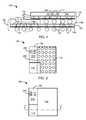
- FIG. 1therein is shown a cross-sectional view of an offset integrated circuit package-on-package stacking system 100 , in an embodiment of the present invention.
- the cross-sectional view of the offset integrated circuit package-on-package stacking system 100depicts a base package 102 , such as a ball grid array package, having a base substrate 104 with a base top surface 106 and a base bottom surface 108 .
- a first integrated circuit 110is mounted on the base top surface 106 with an adhesive 112 , such as die attach material.
- the first integrated circuit 110is coupled to the base top surface 106 by electrical interconnects 114 , such as bond wires, solder bumps, solder columns or stud bumps.
- An offset package 120having an offset substrate 122 with a top surface 124 and a bottom surface 126 , is mounted in an offset position on the base package 102 .
- the offset package 120has a second integrated circuit 128 mounted on the top surface 124 with the adhesive 112 .
- the second integrated circuit 128is coupled to the top surface 124 by the electrical interconnects 114 .
- An offset package body 130such as the molding compound, is injection molded over the second integrated circuit 128 , the top surface 124 and the electrical interconnects 114 .
- the system interconnects 118are attached to the bottom surface 126 , of the offset substrate 122 .
- the offset package 120is mounted on the base package 102 , so that the bottom surface 126 of the offset substrate 122 rests on the base package body 116 and the system interconnects 118 .
- This configurationreduces the space required on a printed circuit board (not shown), while maintaining a low profile over a portion of the offset integrated circuit package-on-package stacking system 100 .
- FIG. 2therein is shown a top view of the base package 102 for the offset integrated circuit package-on-package stacking system 100 , in an embodiment of the present invention.
- the top view of the base package 102 , of FIG. 1depicts the base package body 116 , of FIG. 1 , on the base top surface 106 , of FIG. 1 , with an array of the contact pad 119 , of FIG. 1 , and a passive component 204 .
- An outline 206indicates the area that will be covered by the offset package 120 , of FIG. 1 .
- the array of the contact pad 119is spaced to align with the system interconnects 118 , of FIG. 1 , of the offset package 120 , of FIG. 1 .
- the non-symmetrical array of the contact pad 119allows the offset package 120 to extend over the base package body 116 .
- FIG. 3therein is shown a top view of an assembled package 300 of the offset integrated circuit package-on-package stacking system 100 , in an embodiment of the present invention.
- the top view of the assembled package 300depicts the base top surface 106 having the base package body 116 , the passive component 204 and the offset package 120 mounted thereon.
- a section line 4 - 4shows the position of the view in FIG. 4 .
- FIG. 4therein is shown a cross-sectional view of the offset integrated circuit package-on-package stacking system 100 , of FIG. 3 along the section line 4 - 4 .
- the cross-sectional view of the offset integrated circuit package-on-package stacking system 100depicts the base package 102 with the offset package 120 mounted thereon.
- the bottom surface 126 of the offset substrate 122is on the base package body 116 .
- the base package body 116supports the offset package 120 during the reflow process preventing collapse of the system interconnects 118 .
- FIG. 5therein is shown a cross-sectional view of an offset integrated circuit package-on-package stacking system 500 , in an alternative embodiment of the present invention.
- the cross-sectional view of the offset integrated circuit package-on-package stacking system 500depicts the base package 102 having the offset package 120 coupled electrically through the system interconnects 118 .
- a gap filler adhesive 502such as die attach material or epoxy resin, is applied between the base package body 116 and the bottom surface 126 of the offset substrate 122 . The application of the gap filler adhesive 502 provides additional mechanical stability to the package structure.
- FIG. 6therein is shown a top view of a base package 600 for the offset integrated circuit package-on-package stacking system 100 , in an alternative embodiment of the present invention.
- the top view of the base package 600depicts a base substrate top 602 having a base mold cap 604 , an array of a system contact 606 and an outline 608 , indicating the region that would be covered by the addition of the offset package 120 , of FIG. 1 .
- FIG. 7therein is shown a top view of a base package 700 for the offset integrated circuit package-on-package stacking system 100 , in another alternative embodiment of the present invention.
- the top view of the base package 700depicts a base substrate top 702 , having a base mold cap 704 an array of a contact pad 706 , partially distributed around the base mold cap 704 .
- An outline 708indicates the region that would be covered by the addition of the offset package 120 , of FIG. 1 , should it be added.
- the array of the contact pad 706provides an electrical interface between the base package 700 and the offset package 120 .
- FIG. 8therein is shown a top view of a base package 800 the offset integrated circuit package-on-package stacking system, in yet another alternative embodiment of the present invention.
- the top view of the base package 800depicts a base substrate top 802 having a base mold cap 804 , an array of a system contact pads 806 , an active element 808 , such as a flipchip integrated circuit, the passive component 204 , and an offset package outline 810 , indicating the region that would be covered by the addition of the offset package 120 , of FIG. 1 .
- An overlap region 812indicates the contact area between the base mold cap 804 and the offset package 120 .
- the corner of the base mold cap 804will be covered by the offset package 120 which will rest on the base mold cap 804 .
- the active element 808is placed beneath the offset package 120 and does not contact the bottom surface 126 , of FIG. 1 , of the offset substrate 122 , of FIG. 1 .
- FIG. 9therein is shown a top view of a base package 900 the offset integrated circuit package-on-package stacking system 100 , in yet another alternative embodiment of the present invention.
- the top view of the base package 900depicts a base substrate top 902 having a base mold cap 904 , an array of a system contact pads 906 , the active element 808 , of FIG. 8 , such as a small-outline integrated circuit, the passive component 204 , and an offset package outline 910 , indicating the region that would be covered by the addition of the offset package 120 , of FIG. 1 .
- the offset package 120will rest on the base mold cap 904 with offset package aligned with the edge of the base mold cap.
- the active element 808may be an active small-outline integrated circuit component that is electrically connected to the circuit within the base package 900 , the array of the system contact pads, or a combination thereof.
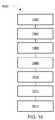
- FIG. 10therein is shown a flow chart of an offset integrated circuit package-on-package stacking system 1000 for manufacturing the offset integrated circuit package-on-package stacking system 100 , in accordance with an embodiment of the present invention.
- the system 1000includes providing a base substrate in a block 1002 ; forming a contact pad on the base substrate in a block 1004 ; mounting a first integrated circuit on the base substrate in a block 1006 ; forming a base package body around the first integrated circuit in a block 1008 ; providing an offset substrate in a block 1010 ; mounting a second integrated circuit on the offset substrate in a block 1012 ; and coupling the offset substrate to the contact pad, including placing the offset substrate on the base package body in a block 1014 .
- a system to manufacture an offset integrated circuit package-on-package stacking systemis performed as follows:
- a principle aspectis that the present invention has the flexibility to add additional components on the base substrate without adding additional package size.
- Yet another important aspect of the present inventionis that it valuably supports and services the historical trend of reducing costs, simplifying systems, and increasing performance.
- the offset integrated circuit package-on-package stacking system of the present inventionfurnishes important and heretofore unknown and unavailable solutions, capabilities, and functional aspects for increasing the integrated circuit density in consumer electronics that have diminished available space.
- the resulting processes and configurationsare straightforward, cost-effective, uncomplicated, highly versatile and effective, can be implemented by adapting known technologies, and are thus readily suited for efficiently and economically manufacturing offset integrated circuit package-on-package stacked devices fully compatible with conventional manufacturing processes and technologies.
Landscapes
- Engineering & Computer Science (AREA)
- Microelectronics & Electronic Packaging (AREA)
- Power Engineering (AREA)
- Physics & Mathematics (AREA)
- Condensed Matter Physics & Semiconductors (AREA)
- General Physics & Mathematics (AREA)
- Computer Hardware Design (AREA)
- Structures Or Materials For Encapsulating Or Coating Semiconductor Devices Or Solid State Devices (AREA)
- Wire Bonding (AREA)
- Amplifiers (AREA)
Abstract
Description
- This application claims the benefit of U.S. Provisional Patent Application Ser. number 60/594,884 filed May 16, 2005.
- The present application contains subject matter related to a concurrently filed U.S. Patent Application by Shim et al. entitled “Offset Integrated Circuit Package-on-Package Stacking System”. The related application is assigned to STATS ChipPAC Ltd. and is identified by docket number 27-173.
- The present invention relates generally to integrated circuit package systems, and more particularly to a system for integrated circuit package systems having stacked packages.
- In order to interface an integrated circuit with other circuitry, it is common to mount it on a lead frame or substrate. Each integrated circuit has bonding pads that are individually connected to the lead frame's lead finger pads using extremely fine gold or aluminum wires. The assemblies are then packaged by individually encapsulating them in molded plastic or ceramic bodies to create an integrated circuit package.
- Integrated circuit packaging technology has seen an increase in the number of integrated circuits mounted on a single circuit board or substrate. The new packaging designs are more compact in form factors, such as the physical size and shape of an integrated circuit, and providing a significant increase in overall integrated circuit density. However, integrated circuit density continues to be limited by the “real estate” available for mounting individual integrated circuits on a substrate. Even larger form factor systems, such as PC's, compute servers, and storage servers, need more integrated circuits in the same or smaller “real estate”. Particularly acute, the needs for portable personal electronics, such as cell phones, digital cameras, music players, PDA's, and location-based devices, have further driven the need for integrated circuit density.
- This increased integrated circuit density, has led to the development of multi-chip packages in which more than one integrated circuit can be packaged. Each package provides mechanical support for the individual integrated circuits and one or more layers of interconnect lines that enable the integrated circuits to be connected electrically to surrounding circuitry. Current multi-chip packages, also commonly referred to as multi-chip modules, typically consist of a PCB substrate onto which a set of separate integrated circuit components is directly attached. Such multi-chip packages have been found to increase integrated circuit density and miniaturization, improve signal propagation speed, reduce overall integrated circuit size and weight, improve performance, and lower costs--all primary goals of the computer industry.
- Multi-chip packages whether vertically or horizontally arranged, can also present problems because they usually must be pre-assembled before the integrated circuit and integrated circuit connections can be tested. Thus, when integrated circuits are mounted and connected in a multi-chip module, individual integrated circuits and connections cannot be tested individually, and it is not possible to identify known-good-die (“KGD”) before being assembled into larger circuits. Consequently, conventional multi-chip packages lead to assembly process yield problems. This fabrication process, which does not identify KGD, is therefore less reliable and more prone to assembly defects.
- Moreover, vertically stacked integrated circuits in typical multi-chip packages can present problems beyond those of horizontally arranged integrated circuit packages, further complicating the manufacturing process. It is more difficult to test and thus determine the actual failure mode of the individual integrated circuits. Moreover the substrate and integrated circuit are often damaged during assembly or testing, complicating the manufacturing process and increasing costs. The vertically stacked integrated circuit problems can be greater than the benefits.
- Thus, a need still remains for improved packaging methods, systems and designs. In view of the shrinking size of consumer electronics and the demand for more sophisticated functions in the restricted space, it is increasingly critical that answers be found to these problems. In view of the ever increasing commercial competitive pressures, increasing consumer expectations, and diminishing opportunities for meaningful product differentiation in the marketplace, it is increasingly critical that answers be found to these problems. Moreover, the ever-increasing need to save costs, improve efficiencies, and meet such competitive pressures adds even greater urgency to the critical necessity that answers be found to these problems.
- Solutions to these problems have been long sought but prior developments have not taught or suggested any solutions and, thus, solutions to these problems have long eluded those skilled in the art.
- The present invention provides an offset integrated circuit package-on-package stacking system including providing a base substrate, forming a contact pad on the base substrate, mounting a first integrated circuit on the base substrate, forming a base package body around the first integrated circuit, providing an offset substrate, mounting a second integrated circuit on the offset substrate, and coupling the offset substrate to the contact pad, including placing the offset substrate on the base package body.
- Certain embodiments of the invention have other aspects in addition to or in place of those mentioned above. The aspects will become apparent to those skilled in the art from a reading of the following detailed description when taken with reference to the accompanying drawings.
FIG. 1 is a cross-sectional view of an offset integrated circuit package-on-package stacking system, in an embodiment of the present invention;FIG. 2 is a top view of a base package for the offset integrated circuit package-on-package stacking system, in an embodiment of the present invention;FIG. 3 is a top view of an assembled package of the offset integrated circuit package-on-package stacking system, in an embodiment of the present invention;FIG. 4 is a cross-sectional view of the offset integrated circuit package-on-package stacking system, ofFIG. 3 alongsection line 4--4;FIG. 5 is a cross-sectional view of the offset integrated circuit package-on-package stacking system, in an alternative embodiment of the present invention;FIG. 6 is a top view of the base package for the offset integrated circuit package-on-package stacking system, in an alternative embodiment of the present invention;FIG. 7 is a top view of the base package for the offset integrated circuit package-on-package stacking system, in another alternative embodiment of the present invention;FIG. 8 is a top view of the base package for the offset integrated circuit package-on-package stacking system, in yet another alternative embodiment of the present invention;FIG. 9 is a top view of the base package for the offset integrated circuit package-on-package stacking system, in still another alternative embodiment of the present invention; andFIG. 10 is a flow chart of an offset integrated circuit package-on-package stacking system for manufacturing the offset integrated circuit package-on-package stacking system in an embodiment of the present invention.- The following embodiments are described in sufficient detail to enable those skilled in the art to make and use the invention. It is to be understood that other embodiments would be evident based on the present disclosure, and that process or mechanical changes may be made without departing from the scope of the present invention.
- In the following description, numerous specific details are given to provide a thorough understanding of the invention. However, it will be apparent that the invention may be practiced without these specific details. In order to avoid obscuring the present invention, some well-known circuits, system configurations, and process steps are not disclosed in detail.
- Likewise, the drawings showing embodiments of the device are semi-diagrammatic and not to scale and, particularly, some of the dimensions are for the clarity of presentation and are shown greatly exaggerated in the drawing FIGS. In addition, where multiple embodiments are disclosed and described having some features in common, for clarity and ease of illustration, description, and comprehension thereof, similar and like features one to another will ordinarily be described with like reference numerals.
- The term “horizontal” as used herein is defined as a plane parallel to the plane or surface of the package substrate, regardless of its orientation. The term “vertical” refers to a direction perpendicular to the horizontal as just defined. Terms, such as “above”, “below”, “bottom”, “top”, “side” (as in “sidewall”), “higher”, “lower”, “upper”, “over”, and “under”, are defined with respect to the horizontal plane. The term “on” means there is direct contact among elements. The term “processing” as used herein includes stamping, forging, patterning, exposure, development, etching, cleaning, and/or removal of the material or laser trimming as required in forming a described structure.
- Referring now to
FIG. 1 , therein is shown a cross-sectional view of an offset integrated circuit package-on-package stacking system 100, in an embodiment of the present invention. The cross-sectional view of the offset integrated circuit package-on-package stacking system 100 depicts abase package 102, such as a ball grid array package, having abase substrate 104 with abase top surface 106 and abase bottom surface 108. A first integratedcircuit 110 is mounted on thebase top surface 106 with an adhesive112, such as die attach material. The first integratedcircuit 110 is coupled to thebase top surface 106 byelectrical interconnects 114, such as bond wires, solder bumps, solder columns or stud bumps. Abase package body 116, such as molding compound, is injection molded around the firstintegrated circuit 110, theelectrical interconnects 114 and a portion of the basetop surface 106. System interconnects118, such as solder balls, solder column interposers or stud bumps, are attached to the basebottom surface 108 for attachment to the next level of system (not shown). An array of acontact pad 119 is distributed in an area around thebase package body 116. - An offset
package 120, having an offsetsubstrate 122 with atop surface 124 and abottom surface 126, is mounted in an offset position on thebase package 102. The offsetpackage 120 has a secondintegrated circuit 128 mounted on thetop surface 124 with the adhesive112. The secondintegrated circuit 128 is coupled to thetop surface 124 by theelectrical interconnects 114. An offsetpackage body 130, such as the molding compound, is injection molded over the secondintegrated circuit 128, thetop surface 124 and theelectrical interconnects 114. The system interconnects118 are attached to thebottom surface 126, of the offsetsubstrate 122. The offsetpackage 120 is mounted on thebase package 102, so that thebottom surface 126 of the offsetsubstrate 122 rests on thebase package body 116 and the system interconnects118. This configuration reduces the space required on a printed circuit board (not shown), while maintaining a low profile over a portion of the offset integrated circuit package-on-package stacking system 100. - Referring now to
FIG. 2 , therein is shown a top view of thebase package 102 for the offset integrated circuit package-on-package stacking system 100, in an embodiment of the present invention. The top view of thebase package 102, ofFIG. 1 , depicts thebase package body 116, ofFIG. 1 , on the basetop surface 106, ofFIG. 1 , with an array of thecontact pad 119, ofFIG. 1 , and apassive component 204. Anoutline 206 indicates the area that will be covered by the offsetpackage 120, ofFIG. 1 . The array of thecontact pad 119 is spaced to align with the system interconnects118, ofFIG. 1 , of the offsetpackage 120, ofFIG. 1 . The non-symmetrical array of thecontact pad 119 allows the offsetpackage 120 to extend over thebase package body 116. - Referring now to
FIG. 3 , therein is shown a top view of an assembledpackage 300 of the offset integrated circuit package-on-package stacking system 100, in an embodiment of the present invention. The top view of the assembledpackage 300 depicts the basetop surface 106 having thebase package body 116, thepassive component 204 and the offsetpackage 120 mounted thereon. A section line4-4 shows the position of the view inFIG. 4 . - Referring now to
FIG. 4 , therein is shown a cross-sectional view of the offset integrated circuit package-on-package stacking system 100, ofFIG. 3 along the section line4-4. The cross-sectional view of the offset integrated circuit package-on-package stacking system 100 depicts thebase package 102 with the offsetpackage 120 mounted thereon. Thebottom surface 126 of the offsetsubstrate 122 is on thebase package body 116. Thebase package body 116 supports the offsetpackage 120 during the reflow process preventing collapse of the system interconnects118. - Referring now to
FIG. 5 , therein is shown a cross-sectional view of an offset integrated circuit package-on-package stacking system 500, in an alternative embodiment of the present invention. The cross-sectional view of the offset integrated circuit package-on-package stacking system 500 depicts thebase package 102 having the offsetpackage 120 coupled electrically through the system interconnects118. Agap filler adhesive 502, such as die attach material or epoxy resin, is applied between thebase package body 116 and thebottom surface 126 of the offsetsubstrate 122. The application of thegap filler adhesive 502 provides additional mechanical stability to the package structure. - Referring now to
FIG. 6 , therein is shown a top view of abase package 600 for the offset integrated circuit package-on-package stacking system 100, in an alternative embodiment of the present invention. The top view of thebase package 600 depicts abase substrate top 602 having abase mold cap 604, an array of asystem contact 606 and anoutline 608, indicating the region that would be covered by the addition of the offsetpackage 120, ofFIG. 1 . - Referring now to
FIG. 7 , therein is shown a top view of abase package 700 for the offset integrated circuit package-on-package stacking system 100, in another alternative embodiment of the present invention. The top view of thebase package 700 depicts abase substrate top 702, having a base mold cap704 an array of acontact pad 706, partially distributed around the base mold cap704. Anoutline 708 indicates the region that would be covered by the addition of the offsetpackage 120, ofFIG. 1 , should it be added. The array of thecontact pad 706 provides an electrical interface between thebase package 700 and the offsetpackage 120. - Referring now to
FIG. 8 , therein is shown a top view of abase package 800 the offset integrated circuit package-on-package stacking system, in yet another alternative embodiment of the present invention. The top view of thebase package 800 depicts abase substrate top 802 having abase mold cap 804, an array of asystem contact pads 806, anactive element 808, such as a flipchip integrated circuit, thepassive component 204, and an offsetpackage outline 810, indicating the region that would be covered by the addition of the offsetpackage 120, ofFIG. 1 . An overlap region812 indicates the contact area between thebase mold cap 804 and the offsetpackage 120. The corner of thebase mold cap 804 will be covered by the offsetpackage 120 which will rest on thebase mold cap 804. Theactive element 808 is placed beneath the offsetpackage 120 and does not contact thebottom surface 126, ofFIG. 1 , of the offsetsubstrate 122, ofFIG. 1 . - Referring now to
FIG. 9 , therein is shown a top view of abase package 900 the offset integrated circuit package-on-package stacking system 100, in yet another alternative embodiment of the present invention. The top view of thebase package 900 depicts abase substrate top 902 having abase mold cap 904, an array of asystem contact pads 906, theactive element 808, ofFIG. 8 , such as a small-outline integrated circuit, thepassive component 204, and an offsetpackage outline 910, indicating the region that would be covered by the addition of the offsetpackage 120, ofFIG. 1 . The offsetpackage 120 will rest on thebase mold cap 904 with offset package aligned with the edge of the base mold cap. Theactive element 808 may be an active small-outline integrated circuit component that is electrically connected to the circuit within thebase package 900, the array of the system contact pads, or a combination thereof Referring now toFIG. 10 , therein is shown a flow chart of an offset integrated circuit package-on-package stacking system 1000 for manufacturing the offset integrated circuit package-on-package stacking system 100, in accordance with an embodiment of the present invention. Thesystem 1000 includes providing a base substrate in ablock 1002; forming a contact pad on the base substrate in ablock 1004; mounting a first integrated circuit on the base substrate in ablock 1006; forming a base package body around the first integrated circuit in ablock 1008; providing an offset substrate in ablock 1010; mounting a second integrated circuit on the offset substrate in ablock 1012; and coupling the offset substrate to the contact pad, including placing the offset substrate on the base package body in ablock 1014. - In greater detail, a system to manufacture an offset integrated circuit package-on-package stacking system, according to an embodiment of the present invention, is performed as follows:
- 1. Providing a base substrate having system interconnects. (
FIG. 1 ) - 2. Forming a contact pad on the base substrate. (
FIG. 1 ) - 3. Mounting a first integrated circuit on the base substrate, including coupling the first integrated circuit to the contact pad. (
FIG. 1 ) - 4. Forming a base package body around the first integrated circuit, including injecting a molding compound. (
FIG. 1 ) - 5. Providing an offset substrate including providing the system interconnects. (
FIG. 1 ) - 6. Mounting a second integrated circuit on the offset substrate including forming an offset package body over the second integrated circuit. (
FIG. 1 ) and - 7. Coupling the offset substrate to the contact pad, including placing the offset substrate on the base package body. (
FIG. 1 )
- 1. Providing a base substrate having system interconnects. (
- It has been discovered that the present invention thus has numerous aspects.
- It has been discovered that in consumer electronic devices, where space is at a premium, the offset integrated circuit package-on-package stacking system can add more function in a limited space.
- A principle aspect is that the present invention has the flexibility to add additional components on the base substrate without adding additional package size.
- Yet another important aspect of the present invention is that it valuably supports and services the historical trend of reducing costs, simplifying systems, and increasing performance.
- These and other valuable aspects of the present invention consequently further the state of the technology to at least the next level.
- Thus, it has been discovered that the offset integrated circuit package-on-package stacking system of the present invention furnishes important and heretofore unknown and unavailable solutions, capabilities, and functional aspects for increasing the integrated circuit density in consumer electronics that have diminished available space. The resulting processes and configurations are straightforward, cost-effective, uncomplicated, highly versatile and effective, can be implemented by adapting known technologies, and are thus readily suited for efficiently and economically manufacturing offset integrated circuit package-on-package stacked devices fully compatible with conventional manufacturing processes and technologies.
- While the invention has been described in conjunction with a specific best mode, it is to be understood that many alternatives, modifications, and variations will be apparent to those skilled in the art in light of the aforegoing description. Accordingly, it is intended to embrace all such alternatives, modifications, and variations which fall within the scope of the included claims. All matters hithertofore set forth herein or shown in the accompanying drawings are to be interpreted in an illustrative and non-limiting sense.
Claims (20)
Priority Applications (4)
| Application Number | Priority Date | Filing Date | Title |
|---|---|---|---|
| US11/383,403US7518224B2 (en) | 2005-05-16 | 2006-05-15 | Offset integrated circuit package-on-package stacking system |
| JP2006136747AJP4402074B2 (en) | 2005-05-16 | 2006-05-16 | Offset integrated circuit package-on-package stacking system and manufacturing method thereof |
| TW095117221ATWI334639B (en) | 2005-05-16 | 2006-05-16 | Offset integrated circuit package-on-package stacking system and method for fabricating the same |
| KR1020060043994AKR101076062B1 (en) | 2005-05-16 | 2006-05-16 | Offset integrated circuit package-on-package stacking system |
Applications Claiming Priority (2)
| Application Number | Priority Date | Filing Date | Title |
|---|---|---|---|
| US59488405P | 2005-05-16 | 2005-05-16 | |
| US11/383,403US7518224B2 (en) | 2005-05-16 | 2006-05-15 | Offset integrated circuit package-on-package stacking system |
Publications (2)
| Publication Number | Publication Date |
|---|---|
| US20070108581A1true US20070108581A1 (en) | 2007-05-17 |
| US7518224B2 US7518224B2 (en) | 2009-04-14 |
Family
ID=38038592
Family Applications (1)
| Application Number | Title | Priority Date | Filing Date |
|---|---|---|---|
| US11/383,403Active2026-11-17US7518224B2 (en) | 2005-05-16 | 2006-05-15 | Offset integrated circuit package-on-package stacking system |
Country Status (4)
| Country | Link |
|---|---|
| US (1) | US7518224B2 (en) |
| JP (1) | JP4402074B2 (en) |
| KR (1) | KR101076062B1 (en) |
| TW (1) | TWI334639B (en) |
Cited By (18)
| Publication number | Priority date | Publication date | Assignee | Title |
|---|---|---|---|---|
| US20090008763A1 (en)* | 2007-07-06 | 2009-01-08 | Samsung Electronics Co., Ltd. | Semiconductor package |
| US20090057861A1 (en)* | 2007-08-31 | 2009-03-05 | Soo-San Park | Integrated circuit package-in-package system with side-by-side and offset stacking |
| US20090057864A1 (en)* | 2007-08-31 | 2009-03-05 | Daesik Choi | Integrated circuit package system employing an offset stacked configuration |
| US20090152700A1 (en)* | 2007-12-12 | 2009-06-18 | Heap Hoe Kuan | Mountable integrated circuit package system with mountable integrated circuit die |
| US20090152692A1 (en)* | 2007-12-12 | 2009-06-18 | Seng Guan Chow | Integrated circuit package system with offset stacking |
| US20090152706A1 (en)* | 2007-12-12 | 2009-06-18 | Heap Hoe Kuan | Integrated circuit package system with interconnect lock |
| US20090155960A1 (en)* | 2007-12-12 | 2009-06-18 | Seng Guan Chow | Integrated circuit package system with offset stacking and anti-flash structure |
| US20090230532A1 (en)* | 2008-03-11 | 2009-09-17 | Stats Chippac Ltd | System for solder ball inner stacking module connection |
| US20090243069A1 (en)* | 2008-03-26 | 2009-10-01 | Zigmund Ramirez Camacho | Integrated circuit package system with redistribution |
| US20100025833A1 (en)* | 2008-07-30 | 2010-02-04 | Reza Argenty Pagaila | Rdl patterning with package on package system |
| US20100155918A1 (en)* | 2008-12-19 | 2010-06-24 | Geun Sik Kim | Integrated circuit packaging system with package stacking and method of manufacture thereof |
| US20120074595A1 (en)* | 2010-09-28 | 2012-03-29 | Samsung Electronics Co., Ltd. | Semiconductor package |
| CN106663674A (en)* | 2014-04-30 | 2017-05-10 | 英特尔公司 | Integrated circuit assembly with molding compound |
| US9871007B2 (en)* | 2015-09-25 | 2018-01-16 | Intel Corporation | Packaged integrated circuit device with cantilever structure |
| US10631410B2 (en) | 2016-09-24 | 2020-04-21 | Apple Inc. | Stacked printed circuit board packages |
| US11257743B2 (en) | 2015-10-29 | 2022-02-22 | Intel Corporation | Guard ring design enabling in-line testing of silicon bridges for semiconductor packages |
| US11508663B2 (en)* | 2018-02-02 | 2022-11-22 | Marvell Israel (M.I.S.L) Ltd. | PCB module on package |
| US11581292B2 (en) | 2019-06-10 | 2023-02-14 | Marvell Israel (M.I.S.L) Ltd. | IC package with top-side memory module |
Families Citing this family (5)
| Publication number | Priority date | Publication date | Assignee | Title |
|---|---|---|---|---|
| JP5543071B2 (en)* | 2008-01-21 | 2014-07-09 | ピーエスフォー ルクスコ エスエイアールエル | Semiconductor device and semiconductor module having the same |
| US7968995B2 (en)* | 2009-06-11 | 2011-06-28 | Stats Chippac Ltd. | Integrated circuit packaging system with package-on-package and method of manufacture thereof |
| US8508045B2 (en)* | 2011-03-03 | 2013-08-13 | Broadcom Corporation | Package 3D interconnection and method of making same |
| US10163877B2 (en)* | 2011-11-07 | 2018-12-25 | Taiwan Semiconductor Manufacturing Co., Ltd. | System in package process flow |
| KR102021077B1 (en)* | 2013-01-24 | 2019-09-11 | 삼성전자주식회사 | Stacked die package, system having the die package, manufacturing method thereof |
Citations (32)
| Publication number | Priority date | Publication date | Assignee | Title |
|---|---|---|---|---|
| US5579207A (en)* | 1994-10-20 | 1996-11-26 | Hughes Electronics | Three-dimensional integrated circuit stacking |
| US5748452A (en)* | 1996-07-23 | 1998-05-05 | International Business Machines Corporation | Multi-electronic device package |
| US5854507A (en)* | 1998-07-21 | 1998-12-29 | Hewlett-Packard Company | Multiple chip assembly |
| US5907903A (en)* | 1996-05-24 | 1999-06-01 | International Business Machines Corporation | Multi-layer-multi-chip pyramid and circuit board structure and method of forming same |
| US6239496B1 (en)* | 1999-01-18 | 2001-05-29 | Kabushiki Kaisha Toshiba | Package having very thin semiconductor chip, multichip module assembled by the package, and method for manufacturing the same |
| US6388333B1 (en)* | 1999-11-30 | 2002-05-14 | Fujitsu Limited | Semiconductor device having protruding electrodes higher than a sealed portion |
| US6410983B1 (en)* | 1999-05-26 | 2002-06-25 | Fujitsu Limited | Semiconductor device having a plurality of multi-chip modules interconnected by a wiring board having an interface LSI chip |
| US6433412B2 (en)* | 2000-03-17 | 2002-08-13 | Hitachi, Ltd. | Semiconductor device and a method of manufacturing the same |
| US6518659B1 (en)* | 2000-05-08 | 2003-02-11 | Amkor Technology, Inc. | Stackable package having a cavity and a lid for an electronic device |
| US6605875B2 (en)* | 1999-12-30 | 2003-08-12 | Intel Corporation | Integrated circuit die having bond pads near adjacent sides to allow stacking of dice without regard to dice size |
| US6667544B1 (en)* | 2000-06-30 | 2003-12-23 | Amkor Technology, Inc. | Stackable package having clips for fastening package and tool for opening clips |
| US20040021230A1 (en)* | 2002-08-05 | 2004-02-05 | Macronix International Co., Ltd. | Ultra thin stacking packaging device |
| US20040026789A1 (en)* | 2002-08-08 | 2004-02-12 | Mitsubishi Denki Kabushiki Kaisha | Semiconductor device |
| US20040036182A1 (en)* | 2002-04-08 | 2004-02-26 | Corisis David J. | Bond pad rerouting element and stacked semiconductor device assemblies including the rerouting element |
| US6731009B1 (en)* | 2000-03-20 | 2004-05-04 | Cypress Semiconductor Corporation | Multi-die assembly |
| US6740980B2 (en)* | 2002-07-04 | 2004-05-25 | Renesas Technology Corp. | Semiconductor device |
| US6798057B2 (en)* | 2002-11-05 | 2004-09-28 | Micron Technology, Inc. | Thin stacked ball-grid array package |
| US20040195700A1 (en)* | 2003-04-04 | 2004-10-07 | Advanced Semiconductor Engineering Inc. | Multi-chip package combining wire-bonding and flip-chip configuration |
| US6897553B2 (en)* | 1998-03-09 | 2005-05-24 | Micron Technology, Inc. | Apparatus for forming a stack of packaged memory dice |
| US6899534B2 (en)* | 1997-07-09 | 2005-05-31 | Micron Technology, Inc. | Mold assembly for a package stack via bottom-leaded plastic (blp) packaging |
| US7061087B2 (en)* | 2002-10-24 | 2006-06-13 | Samsung Electronics Co., Ltd. | Multi-package stack module |
| US20060139902A1 (en)* | 2004-12-28 | 2006-06-29 | Kabushiki Kaisha Toshiba | Double-sided component-mounted circuit board and method for manufacturing the same |
| US7075188B2 (en)* | 2003-02-28 | 2006-07-11 | Sanyo Electric Co., Ltd. | Circuit device and method for manufacturing the same |
| US7087989B2 (en)* | 2003-05-30 | 2006-08-08 | Seiko Epson Corporation | Semiconductor device, electronic device, electronic apparatus, and method of manufacturing semiconductor device |
| US7091581B1 (en)* | 2004-06-14 | 2006-08-15 | Asat Limited | Integrated circuit package and process for fabricating the same |
| US7095104B2 (en)* | 2003-11-21 | 2006-08-22 | International Business Machines Corporation | Overlap stacking of center bus bonded memory chips for double density and method of manufacturing the same |
| US7230329B2 (en)* | 2003-02-07 | 2007-06-12 | Seiko Epson Corporation | Semiconductor device, electronic device, electronic equipment, method of manufacturing semiconductor device, and method of manufacturing electronic device |
| US20070241442A1 (en)* | 2006-04-18 | 2007-10-18 | Stats Chippac Ltd. | Stacked integrated circuit package-in-package system |
| US7312519B2 (en)* | 2006-01-12 | 2007-12-25 | Stats Chippac Ltd. | Stacked integrated circuit package-in-package system |
| US20080029858A1 (en)* | 2006-08-03 | 2008-02-07 | Stats Chippac Ltd. | Integrated circuit package-on-package stacking system |
| US20080136006A1 (en)* | 2006-12-09 | 2008-06-12 | Stats Chippac Ltd. | Stacked integrated circuit package-in-package system |
| US20080136007A1 (en)* | 2006-12-09 | 2008-06-12 | Stats Chippac Ltd. | Stacked integrated circuit package-in-package system |
Family Cites Families (2)
| Publication number | Priority date | Publication date | Assignee | Title |
|---|---|---|---|---|
| JP2001044362A (en) | 1999-07-27 | 2001-02-16 | Mitsubishi Electric Corp | Semiconductor device mounting structure and mounting method |
| KR100546359B1 (en) | 2003-07-31 | 2006-01-26 | 삼성전자주식회사 | Semiconductor chip package and stacked module including functional part and mounting part arranged laterally on the same plane |
- 2006
- 2006-05-15USUS11/383,403patent/US7518224B2/enactiveActive
- 2006-05-16TWTW095117221Apatent/TWI334639B/enactive
- 2006-05-16KRKR1020060043994Apatent/KR101076062B1/enactiveActive
- 2006-05-16JPJP2006136747Apatent/JP4402074B2/enactiveActive
Patent Citations (35)
| Publication number | Priority date | Publication date | Assignee | Title |
|---|---|---|---|---|
| US5579207A (en)* | 1994-10-20 | 1996-11-26 | Hughes Electronics | Three-dimensional integrated circuit stacking |
| US5907903A (en)* | 1996-05-24 | 1999-06-01 | International Business Machines Corporation | Multi-layer-multi-chip pyramid and circuit board structure and method of forming same |
| US5748452A (en)* | 1996-07-23 | 1998-05-05 | International Business Machines Corporation | Multi-electronic device package |
| US5963430A (en)* | 1996-07-23 | 1999-10-05 | International Business Machines Corporation | Multi-electronic device package comprising at least two substrates and at least four layers of electrically conductive circuitry |
| US6101100A (en)* | 1996-07-23 | 2000-08-08 | International Business Machines Corporation | Multi-electronic device package |
| US6899534B2 (en)* | 1997-07-09 | 2005-05-31 | Micron Technology, Inc. | Mold assembly for a package stack via bottom-leaded plastic (blp) packaging |
| US6897553B2 (en)* | 1998-03-09 | 2005-05-24 | Micron Technology, Inc. | Apparatus for forming a stack of packaged memory dice |
| US5854507A (en)* | 1998-07-21 | 1998-12-29 | Hewlett-Packard Company | Multiple chip assembly |
| US6239496B1 (en)* | 1999-01-18 | 2001-05-29 | Kabushiki Kaisha Toshiba | Package having very thin semiconductor chip, multichip module assembled by the package, and method for manufacturing the same |
| US6410983B1 (en)* | 1999-05-26 | 2002-06-25 | Fujitsu Limited | Semiconductor device having a plurality of multi-chip modules interconnected by a wiring board having an interface LSI chip |
| US6388333B1 (en)* | 1999-11-30 | 2002-05-14 | Fujitsu Limited | Semiconductor device having protruding electrodes higher than a sealed portion |
| US6605875B2 (en)* | 1999-12-30 | 2003-08-12 | Intel Corporation | Integrated circuit die having bond pads near adjacent sides to allow stacking of dice without regard to dice size |
| US6433412B2 (en)* | 2000-03-17 | 2002-08-13 | Hitachi, Ltd. | Semiconductor device and a method of manufacturing the same |
| US6731009B1 (en)* | 2000-03-20 | 2004-05-04 | Cypress Semiconductor Corporation | Multi-die assembly |
| US6518659B1 (en)* | 2000-05-08 | 2003-02-11 | Amkor Technology, Inc. | Stackable package having a cavity and a lid for an electronic device |
| US6667544B1 (en)* | 2000-06-30 | 2003-12-23 | Amkor Technology, Inc. | Stackable package having clips for fastening package and tool for opening clips |
| US20040036182A1 (en)* | 2002-04-08 | 2004-02-26 | Corisis David J. | Bond pad rerouting element and stacked semiconductor device assemblies including the rerouting element |
| US6740980B2 (en)* | 2002-07-04 | 2004-05-25 | Renesas Technology Corp. | Semiconductor device |
| US20040021230A1 (en)* | 2002-08-05 | 2004-02-05 | Macronix International Co., Ltd. | Ultra thin stacking packaging device |
| US20040026789A1 (en)* | 2002-08-08 | 2004-02-12 | Mitsubishi Denki Kabushiki Kaisha | Semiconductor device |
| US7061087B2 (en)* | 2002-10-24 | 2006-06-13 | Samsung Electronics Co., Ltd. | Multi-package stack module |
| US6798057B2 (en)* | 2002-11-05 | 2004-09-28 | Micron Technology, Inc. | Thin stacked ball-grid array package |
| US7230329B2 (en)* | 2003-02-07 | 2007-06-12 | Seiko Epson Corporation | Semiconductor device, electronic device, electronic equipment, method of manufacturing semiconductor device, and method of manufacturing electronic device |
| US7075188B2 (en)* | 2003-02-28 | 2006-07-11 | Sanyo Electric Co., Ltd. | Circuit device and method for manufacturing the same |
| US20040195700A1 (en)* | 2003-04-04 | 2004-10-07 | Advanced Semiconductor Engineering Inc. | Multi-chip package combining wire-bonding and flip-chip configuration |
| US7087989B2 (en)* | 2003-05-30 | 2006-08-08 | Seiko Epson Corporation | Semiconductor device, electronic device, electronic apparatus, and method of manufacturing semiconductor device |
| US7095104B2 (en)* | 2003-11-21 | 2006-08-22 | International Business Machines Corporation | Overlap stacking of center bus bonded memory chips for double density and method of manufacturing the same |
| US7091581B1 (en)* | 2004-06-14 | 2006-08-15 | Asat Limited | Integrated circuit package and process for fabricating the same |
| US20060139902A1 (en)* | 2004-12-28 | 2006-06-29 | Kabushiki Kaisha Toshiba | Double-sided component-mounted circuit board and method for manufacturing the same |
| US7312519B2 (en)* | 2006-01-12 | 2007-12-25 | Stats Chippac Ltd. | Stacked integrated circuit package-in-package system |
| US20070241442A1 (en)* | 2006-04-18 | 2007-10-18 | Stats Chippac Ltd. | Stacked integrated circuit package-in-package system |
| US7420269B2 (en)* | 2006-04-18 | 2008-09-02 | Stats Chippac Ltd. | Stacked integrated circuit package-in-package system |
| US20080029858A1 (en)* | 2006-08-03 | 2008-02-07 | Stats Chippac Ltd. | Integrated circuit package-on-package stacking system |
| US20080136006A1 (en)* | 2006-12-09 | 2008-06-12 | Stats Chippac Ltd. | Stacked integrated circuit package-in-package system |
| US20080136007A1 (en)* | 2006-12-09 | 2008-06-12 | Stats Chippac Ltd. | Stacked integrated circuit package-in-package system |
Cited By (40)
| Publication number | Priority date | Publication date | Assignee | Title |
|---|---|---|---|---|
| US20090008763A1 (en)* | 2007-07-06 | 2009-01-08 | Samsung Electronics Co., Ltd. | Semiconductor package |
| US20090057861A1 (en)* | 2007-08-31 | 2009-03-05 | Soo-San Park | Integrated circuit package-in-package system with side-by-side and offset stacking |
| US20090057864A1 (en)* | 2007-08-31 | 2009-03-05 | Daesik Choi | Integrated circuit package system employing an offset stacked configuration |
| US8093727B2 (en) | 2007-08-31 | 2012-01-10 | Stats Chippac Ltd. | Integrated circuit package-in-package system with side-by-side and offset stacking and method for manufacturing thereof |
| US8383458B2 (en) | 2007-08-31 | 2013-02-26 | Stats Chippac Ltd. | Integrated circuit package system employing an offset stacked configuration and method for manufacturing thereof |
| US20110084373A1 (en)* | 2007-08-31 | 2011-04-14 | Daesik Choi | Integrated circuit package system employing an offset stacked configuration and method for manufacturing thereof |
| US7872340B2 (en) | 2007-08-31 | 2011-01-18 | Stats Chippac Ltd. | Integrated circuit package system employing an offset stacked configuration |
| US20100320621A1 (en)* | 2007-08-31 | 2010-12-23 | Soo-San Park | Integrated circuit package-in-package system with side-by-side and offset stacking and method for manufacturing thereof |
| US7812435B2 (en) | 2007-08-31 | 2010-10-12 | Stats Chippac Ltd. | Integrated circuit package-in-package system with side-by-side and offset stacking |
| US7985628B2 (en) | 2007-12-12 | 2011-07-26 | Stats Chippac Ltd. | Integrated circuit package system with interconnect lock |
| US8084849B2 (en) | 2007-12-12 | 2011-12-27 | Stats Chippac Ltd. | Integrated circuit package system with offset stacking |
| US7781261B2 (en) | 2007-12-12 | 2010-08-24 | Stats Chippac Ltd. | Integrated circuit package system with offset stacking and anti-flash structure |
| US8536692B2 (en) | 2007-12-12 | 2013-09-17 | Stats Chippac Ltd. | Mountable integrated circuit package system with mountable integrated circuit die |
| US8143711B2 (en) | 2007-12-12 | 2012-03-27 | Stats Chippac Ltd. | Integrated circuit package system with offset stacking and anti-flash structure |
| US20100270680A1 (en)* | 2007-12-12 | 2010-10-28 | Seng Guan Chow | Integrated circuit package system with offset stacking and anti-flash structure |
| US20090152700A1 (en)* | 2007-12-12 | 2009-06-18 | Heap Hoe Kuan | Mountable integrated circuit package system with mountable integrated circuit die |
| US20090155960A1 (en)* | 2007-12-12 | 2009-06-18 | Seng Guan Chow | Integrated circuit package system with offset stacking and anti-flash structure |
| US20090152706A1 (en)* | 2007-12-12 | 2009-06-18 | Heap Hoe Kuan | Integrated circuit package system with interconnect lock |
| US20090152692A1 (en)* | 2007-12-12 | 2009-06-18 | Seng Guan Chow | Integrated circuit package system with offset stacking |
| US8067828B2 (en)* | 2008-03-11 | 2011-11-29 | Stats Chippac Ltd. | System for solder ball inner stacking module connection |
| US20090230532A1 (en)* | 2008-03-11 | 2009-09-17 | Stats Chippac Ltd | System for solder ball inner stacking module connection |
| US20090243069A1 (en)* | 2008-03-26 | 2009-10-01 | Zigmund Ramirez Camacho | Integrated circuit package system with redistribution |
| US20100025833A1 (en)* | 2008-07-30 | 2010-02-04 | Reza Argenty Pagaila | Rdl patterning with package on package system |
| US9293385B2 (en) | 2008-07-30 | 2016-03-22 | Stats Chippac Ltd. | RDL patterning with package on package system |
| US20100155918A1 (en)* | 2008-12-19 | 2010-06-24 | Geun Sik Kim | Integrated circuit packaging system with package stacking and method of manufacture thereof |
| US7785925B2 (en) | 2008-12-19 | 2010-08-31 | Stats Chippac Ltd. | Integrated circuit packaging system with package stacking and method of manufacture thereof |
| US20120074595A1 (en)* | 2010-09-28 | 2012-03-29 | Samsung Electronics Co., Ltd. | Semiconductor package |
| CN106663674A (en)* | 2014-04-30 | 2017-05-10 | 英特尔公司 | Integrated circuit assembly with molding compound |
| DE112014006417B4 (en)* | 2014-04-30 | 2025-07-24 | Sk Hynix Nand Product Solutions Corp. | Integrated circuit arrangement with molding compound |
| US9871007B2 (en)* | 2015-09-25 | 2018-01-16 | Intel Corporation | Packaged integrated circuit device with cantilever structure |
| CN107924910A (en)* | 2015-09-25 | 2018-04-17 | 英特尔公司 | Packaged integrated circuit device with cantilever structure |
| US10490516B2 (en) | 2015-09-25 | 2019-11-26 | Intel Corporation | Packaged integrated circuit device with cantilever structure |
| TWI712111B (en)* | 2015-09-25 | 2020-12-01 | 美商英特爾公司 | Packaged integrated circuit device, method for forming the same and electronic system |
| US11676889B2 (en) | 2015-10-29 | 2023-06-13 | Intel Corporation | Guard ring design enabling in-line testing of silicon bridges for semiconductor packages |
| US11257743B2 (en) | 2015-10-29 | 2022-02-22 | Intel Corporation | Guard ring design enabling in-line testing of silicon bridges for semiconductor packages |
| US12142553B2 (en) | 2015-10-29 | 2024-11-12 | Intel Corporation | Guard ring design enabling in-line testing of silicon bridges for semiconductor packages |
| US10631410B2 (en) | 2016-09-24 | 2020-04-21 | Apple Inc. | Stacked printed circuit board packages |
| US11508663B2 (en)* | 2018-02-02 | 2022-11-22 | Marvell Israel (M.I.S.L) Ltd. | PCB module on package |
| US11967587B2 (en) | 2019-06-10 | 2024-04-23 | Marvell Israel (M.I.S.L) Ltd. | IC package with top-side memory module |
| US11581292B2 (en) | 2019-06-10 | 2023-02-14 | Marvell Israel (M.I.S.L) Ltd. | IC package with top-side memory module |
Also Published As
| Publication number | Publication date |
|---|---|
| KR20060118363A (en) | 2006-11-23 |
| US7518224B2 (en) | 2009-04-14 |
| JP2006324665A (en) | 2006-11-30 |
| TWI334639B (en) | 2010-12-11 |
| KR101076062B1 (en) | 2011-10-21 |
| JP4402074B2 (en) | 2010-01-20 |
| TW200703599A (en) | 2007-01-16 |
Similar Documents
| Publication | Publication Date | Title |
|---|---|---|
| US7518224B2 (en) | Offset integrated circuit package-on-package stacking system | |
| US7746656B2 (en) | Offset integrated circuit package-on-package stacking system | |
| US7535086B2 (en) | Integrated circuit package-on-package stacking system | |
| US7755180B2 (en) | Integrated circuit package-in-package system | |
| US7872340B2 (en) | Integrated circuit package system employing an offset stacked configuration | |
| US8541872B2 (en) | Integrated circuit package system with package stacking and method of manufacture thereof | |
| US8723302B2 (en) | Integrated circuit package system with input/output expansion | |
| US7659609B2 (en) | Integrated circuit package-in-package system with carrier interposer | |
| US7871861B2 (en) | Stacked integrated circuit package system with intra-stack encapsulation | |
| US8084849B2 (en) | Integrated circuit package system with offset stacking | |
| US8536692B2 (en) | Mountable integrated circuit package system with mountable integrated circuit die | |
| US20090140408A1 (en) | Integrated circuit package-on-package system with stacking via interconnect | |
| US7566966B2 (en) | Integrated circuit package-on-package system with anti-mold flash feature | |
| US20080157319A1 (en) | Mountable integrated circuit package-in-package system with adhesive spacing structures | |
| US7871862B2 (en) | Ball grid array package stacking system | |
| US20080171405A1 (en) | Integrated circuit package system with leads having multiple sides exposed | |
| US8093727B2 (en) | Integrated circuit package-in-package system with side-by-side and offset stacking and method for manufacturing thereof |
Legal Events
| Date | Code | Title | Description |
|---|---|---|---|
| AS | Assignment | Owner name:STATS CHIPPAC LTD., SINGAPORE Free format text:CORRECTIVE ASSIGNMENT TO CORRECT THE CORRECTIVE ASSIGNMENT TO RE-RECORD ASSIGNMENT TO CORRECT THE SERIAL NUMBER FROM 11383407 TO 11383403 PREVIOUSLY RECORDED ON REEL 017703 FRAME 0533;ASSIGNORS:SHIM, IL KWON;HAN, BYUNG JOON;CHOW, SENG GUAN;REEL/FRAME:017717/0170;SIGNING DATES FROM 20060518 TO 20060519 Owner name:STATS CHIPPAC LTD.,SINGAPORE Free format text:CORRECTIVE ASSIGNMENT TO CORRECT THE CORRECTIVE ASSIGNMENT TO RE-RECORD ASSIGNMENT TO CORRECT THE SERIAL NUMBER FROM 11383407 TO 11383403 PREVIOUSLY RECORDED ON REEL 017703 FRAME 0533. ASSIGNOR(S) HEREBY CONFIRMS THE ASSIGNMENT;ASSIGNORS:SHIM, IL KWON;HAN, BYUNG JOON;CHOW, SENG GUAN;SIGNING DATES FROM 20060518 TO 20060519;REEL/FRAME:017717/0170 | |
| STCF | Information on status: patent grant | Free format text:PATENTED CASE | |
| CC | Certificate of correction | ||
| FPAY | Fee payment | Year of fee payment:4 | |
| AS | Assignment | Owner name:CITICORP INTERNATIONAL LIMITED, AS COMMON SECURITY AGENT, HONG KONG Free format text:SECURITY INTEREST;ASSIGNORS:STATS CHIPPAC, INC.;STATS CHIPPAC LTD.;REEL/FRAME:036288/0748 Effective date:20150806 Owner name:CITICORP INTERNATIONAL LIMITED, AS COMMON SECURITY Free format text:SECURITY INTEREST;ASSIGNORS:STATS CHIPPAC, INC.;STATS CHIPPAC LTD.;REEL/FRAME:036288/0748 Effective date:20150806 | |
| AS | Assignment | Owner name:STATS CHIPPAC PTE. LTE., SINGAPORE Free format text:CHANGE OF NAME;ASSIGNOR:STATS CHIPPAC LTD.;REEL/FRAME:038378/0319 Effective date:20160329 | |
| FPAY | Fee payment | Year of fee payment:8 | |
| AS | Assignment | Owner name:STATS CHIPPAC, INC., CALIFORNIA Free format text:RELEASE BY SECURED PARTY;ASSIGNOR:CITICORP INTERNATIONAL LIMITED, AS COMMON SECURITY AGENT;REEL/FRAME:052938/0305 Effective date:20190503 Owner name:STATS CHIPPAC PTE. LTD. FORMERLY KNOWN AS STATS CHIPPAC LTD., SINGAPORE Free format text:RELEASE BY SECURED PARTY;ASSIGNOR:CITICORP INTERNATIONAL LIMITED, AS COMMON SECURITY AGENT;REEL/FRAME:052938/0305 Effective date:20190503 | |
| MAFP | Maintenance fee payment | Free format text:PAYMENT OF MAINTENANCE FEE, 12TH YEAR, LARGE ENTITY (ORIGINAL EVENT CODE: M1553); ENTITY STATUS OF PATENT OWNER: LARGE ENTITY Year of fee payment:12 | |
| AS | Assignment | Owner name:STATS CHIPPAC PTE. LTD., SINGAPORE Free format text:CORRECT ERROR IN ASSIGNMENT NAME FROM STATS CHIPPAC, PTE. LTE TO STATS CHIPPAC PTE. LTD (REEL: 038378 FRAME: 0319);ASSIGNOR:STATS CHIPPAC PTE. LTE.;REEL/FRAME:064760/0986 Effective date:20160329 |