US20070107661A1 - Methods, systems, and apparatus for uniform chemical-vapor depositions - Google Patents
Methods, systems, and apparatus for uniform chemical-vapor depositionsDownload PDFInfo
- Publication number
- US20070107661A1 US20070107661A1US11/651,136US65113607AUS2007107661A1US 20070107661 A1US20070107661 A1US 20070107661A1US 65113607 AUS65113607 AUS 65113607AUS 2007107661 A1US2007107661 A1US 2007107661A1
- Authority
- US
- United States
- Prior art keywords
- plate
- chamber
- gas
- substrate
- channels
- Prior art date
- Legal status (The legal status is an assumption and is not a legal conclusion. Google has not performed a legal analysis and makes no representation as to the accuracy of the status listed.)
- Abandoned
Links
- 238000000034methodMethods0.000titleclaimsabstractdescription25
- 238000005229chemical vapour depositionMethods0.000titleclaimsabstractdescription24
- 239000000758substrateSubstances0.000claimsabstractdescription53
- 238000009826distributionMethods0.000claimsabstractdescription41
- 238000000151depositionMethods0.000claimsabstractdescription25
- 230000008021depositionEffects0.000claimsabstractdescription24
- XUIMIQQOPSSXEZ-UHFFFAOYSA-NSiliconChemical compound[Si]XUIMIQQOPSSXEZ-UHFFFAOYSA-N0.000claimsabstractdescription12
- 229910052710siliconInorganic materials0.000claimsabstractdescription12
- 239000010703siliconSubstances0.000claimsabstractdescription12
- 238000005137deposition processMethods0.000claimsabstractdescription4
- 239000007789gasSubstances0.000claimsdescription103
- 238000010438heat treatmentMethods0.000claimsdescription7
- 239000000376reactantSubstances0.000claimsdescription5
- 230000003647oxidationEffects0.000claimsdescription2
- 238000007254oxidation reactionMethods0.000claimsdescription2
- 238000000231atomic layer depositionMethods0.000claims1
- 235000012431wafersNutrition0.000description22
- 239000000463materialSubstances0.000description9
- 238000006243chemical reactionMethods0.000description5
- 238000005516engineering processMethods0.000description3
- 239000002243precursorSubstances0.000description3
- 239000006227byproductSubstances0.000description2
- 239000010795gaseous wasteSubstances0.000description2
- 230000001788irregularEffects0.000description2
- 238000004519manufacturing processMethods0.000description2
- 229910001220stainless steelInorganic materials0.000description2
- 239000010935stainless steelSubstances0.000description2
- 239000002699waste materialSubstances0.000description2
- 230000001154acute effectEffects0.000description1
- 238000000429assemblyMethods0.000description1
- 230000000712assemblyEffects0.000description1
- QVGXLLKOCUKJST-UHFFFAOYSA-Natomic oxygenChemical compound[O]QVGXLLKOCUKJST-UHFFFAOYSA-N0.000description1
- 230000015572biosynthetic processEffects0.000description1
- 239000013590bulk materialSubstances0.000description1
- 230000000295complement effectEffects0.000description1
- 238000010586diagramMethods0.000description1
- 238000001312dry etchingMethods0.000description1
- 238000005530etchingMethods0.000description1
- 239000011521glassSubstances0.000description1
- 238000003780insertionMethods0.000description1
- 230000037431insertionEffects0.000description1
- 239000012212insulatorSubstances0.000description1
- 235000021190leftoversNutrition0.000description1
- 230000000873masking effectEffects0.000description1
- 230000013011matingEffects0.000description1
- 239000000203mixtureSubstances0.000description1
- 239000001301oxygenSubstances0.000description1
- 229910052760oxygenInorganic materials0.000description1
- 238000000059patterningMethods0.000description1
- 238000001020plasma etchingMethods0.000description1
- 229920006254polymer filmPolymers0.000description1
- 239000000047productSubstances0.000description1
- 230000001737promoting effectEffects0.000description1
- 229910052594sapphireInorganic materials0.000description1
- 239000010980sapphireSubstances0.000description1
- 239000004065semiconductorSubstances0.000description1
- 239000000126substanceSubstances0.000description1
- 230000002123temporal effectEffects0.000description1
- 238000009827uniform distributionMethods0.000description1
- 238000001039wet etchingMethods0.000description1
Images


Classifications
- C—CHEMISTRY; METALLURGY
- C23—COATING METALLIC MATERIAL; COATING MATERIAL WITH METALLIC MATERIAL; CHEMICAL SURFACE TREATMENT; DIFFUSION TREATMENT OF METALLIC MATERIAL; COATING BY VACUUM EVAPORATION, BY SPUTTERING, BY ION IMPLANTATION OR BY CHEMICAL VAPOUR DEPOSITION, IN GENERAL; INHIBITING CORROSION OF METALLIC MATERIAL OR INCRUSTATION IN GENERAL
- C23C—COATING METALLIC MATERIAL; COATING MATERIAL WITH METALLIC MATERIAL; SURFACE TREATMENT OF METALLIC MATERIAL BY DIFFUSION INTO THE SURFACE, BY CHEMICAL CONVERSION OR SUBSTITUTION; COATING BY VACUUM EVAPORATION, BY SPUTTERING, BY ION IMPLANTATION OR BY CHEMICAL VAPOUR DEPOSITION, IN GENERAL
- C23C16/00—Chemical coating by decomposition of gaseous compounds, without leaving reaction products of surface material in the coating, i.e. chemical vapour deposition [CVD] processes
- C23C16/44—Chemical coating by decomposition of gaseous compounds, without leaving reaction products of surface material in the coating, i.e. chemical vapour deposition [CVD] processes characterised by the method of coating
- C23C16/455—Chemical coating by decomposition of gaseous compounds, without leaving reaction products of surface material in the coating, i.e. chemical vapour deposition [CVD] processes characterised by the method of coating characterised by the method used for introducing gases into reaction chamber or for modifying gas flows in reaction chamber
- C23C16/45563—Gas nozzles
- C23C16/45565—Shower nozzles
- C—CHEMISTRY; METALLURGY
- C23—COATING METALLIC MATERIAL; COATING MATERIAL WITH METALLIC MATERIAL; CHEMICAL SURFACE TREATMENT; DIFFUSION TREATMENT OF METALLIC MATERIAL; COATING BY VACUUM EVAPORATION, BY SPUTTERING, BY ION IMPLANTATION OR BY CHEMICAL VAPOUR DEPOSITION, IN GENERAL; INHIBITING CORROSION OF METALLIC MATERIAL OR INCRUSTATION IN GENERAL
- C23C—COATING METALLIC MATERIAL; COATING MATERIAL WITH METALLIC MATERIAL; SURFACE TREATMENT OF METALLIC MATERIAL BY DIFFUSION INTO THE SURFACE, BY CHEMICAL CONVERSION OR SUBSTITUTION; COATING BY VACUUM EVAPORATION, BY SPUTTERING, BY ION IMPLANTATION OR BY CHEMICAL VAPOUR DEPOSITION, IN GENERAL
- C23C16/00—Chemical coating by decomposition of gaseous compounds, without leaving reaction products of surface material in the coating, i.e. chemical vapour deposition [CVD] processes
- C23C16/44—Chemical coating by decomposition of gaseous compounds, without leaving reaction products of surface material in the coating, i.e. chemical vapour deposition [CVD] processes characterised by the method of coating
- C23C16/455—Chemical coating by decomposition of gaseous compounds, without leaving reaction products of surface material in the coating, i.e. chemical vapour deposition [CVD] processes characterised by the method of coating characterised by the method used for introducing gases into reaction chamber or for modifying gas flows in reaction chamber
- C23C16/45523—Pulsed gas flow or change of composition over time
- C23C16/45525—Atomic layer deposition [ALD]
- C23C16/45544—Atomic layer deposition [ALD] characterized by the apparatus
- C—CHEMISTRY; METALLURGY
- C23—COATING METALLIC MATERIAL; COATING MATERIAL WITH METALLIC MATERIAL; CHEMICAL SURFACE TREATMENT; DIFFUSION TREATMENT OF METALLIC MATERIAL; COATING BY VACUUM EVAPORATION, BY SPUTTERING, BY ION IMPLANTATION OR BY CHEMICAL VAPOUR DEPOSITION, IN GENERAL; INHIBITING CORROSION OF METALLIC MATERIAL OR INCRUSTATION IN GENERAL
- C23C—COATING METALLIC MATERIAL; COATING MATERIAL WITH METALLIC MATERIAL; SURFACE TREATMENT OF METALLIC MATERIAL BY DIFFUSION INTO THE SURFACE, BY CHEMICAL CONVERSION OR SUBSTITUTION; COATING BY VACUUM EVAPORATION, BY SPUTTERING, BY ION IMPLANTATION OR BY CHEMICAL VAPOUR DEPOSITION, IN GENERAL
- C23C16/00—Chemical coating by decomposition of gaseous compounds, without leaving reaction products of surface material in the coating, i.e. chemical vapour deposition [CVD] processes
- C23C16/44—Chemical coating by decomposition of gaseous compounds, without leaving reaction products of surface material in the coating, i.e. chemical vapour deposition [CVD] processes characterised by the method of coating
- C23C16/455—Chemical coating by decomposition of gaseous compounds, without leaving reaction products of surface material in the coating, i.e. chemical vapour deposition [CVD] processes characterised by the method of coating characterised by the method used for introducing gases into reaction chamber or for modifying gas flows in reaction chamber
- C23C16/45587—Mechanical means for changing the gas flow
- C23C16/45589—Movable means, e.g. fans
- C—CHEMISTRY; METALLURGY
- C23—COATING METALLIC MATERIAL; COATING MATERIAL WITH METALLIC MATERIAL; CHEMICAL SURFACE TREATMENT; DIFFUSION TREATMENT OF METALLIC MATERIAL; COATING BY VACUUM EVAPORATION, BY SPUTTERING, BY ION IMPLANTATION OR BY CHEMICAL VAPOUR DEPOSITION, IN GENERAL; INHIBITING CORROSION OF METALLIC MATERIAL OR INCRUSTATION IN GENERAL
- C23C—COATING METALLIC MATERIAL; COATING MATERIAL WITH METALLIC MATERIAL; SURFACE TREATMENT OF METALLIC MATERIAL BY DIFFUSION INTO THE SURFACE, BY CHEMICAL CONVERSION OR SUBSTITUTION; COATING BY VACUUM EVAPORATION, BY SPUTTERING, BY ION IMPLANTATION OR BY CHEMICAL VAPOUR DEPOSITION, IN GENERAL
- C23C16/00—Chemical coating by decomposition of gaseous compounds, without leaving reaction products of surface material in the coating, i.e. chemical vapour deposition [CVD] processes
- C23C16/44—Chemical coating by decomposition of gaseous compounds, without leaving reaction products of surface material in the coating, i.e. chemical vapour deposition [CVD] processes characterised by the method of coating
- C23C16/455—Chemical coating by decomposition of gaseous compounds, without leaving reaction products of surface material in the coating, i.e. chemical vapour deposition [CVD] processes characterised by the method of coating characterised by the method used for introducing gases into reaction chamber or for modifying gas flows in reaction chamber
- C23C16/45587—Mechanical means for changing the gas flow
- C23C16/45591—Fixed means, e.g. wings, baffles
Definitions
- This inventionconcerns methods of making integrated circuits, particularly layer-formation, such as chemical-vapor deposition.
- Integrated circuitsthe key components in thousands of electronic and computer products, are interconnected networks of electrical components fabricated on a common foundation, or substrate. Fabricators generally build these circuits layer by layer, using techniques, such as deposition, doping, masking, and etching, to form thousands and even millions of microscopic resistors, transistors, and other electrical components on a silicon substrate, known as a wafer. The components are then wired, or interconnected, together to define a specific electric circuit, such as a computer memory.
- Chemical vapor depositiongenerally entails placing a substrate in a reaction chamber, heating the substrate to prescribed temperatures, and introducing one or more gases, known as precursor gases, into the chamber to begin a deposition cycle.
- the precursor gasesenter the chamber through a gas-distribution fixture, such as a gas ring or a showerhead, one or more centimeters above the substrate, and descend toward the heated substrate.
- the gasesreact with each other and/or the heated substrate, blanketing its surface with a layer of material.
- An exhaust systemthen pumps gaseous by-products or leftovers from the reaction out of the chamber through a separate outlet to complete the deposition cycle.
- CVDchemical-vapor-deposition
- Conventional chemical-vapor-deposition (CVD) systemssuffer from at least two problems.
- First, conventional CVD systemsgenerally form layers that include microscopic hills and valleys and thus have non-uniform thickness.
- fabricatorshave been able to overcome these hills and valleys through use of post-deposition planarization or other compensation techniques.
- escalating demands for greater circuit density, for thinner layers, and for larger substratesmake it increasingly difficult, if not completely impractical, to overcome the non-uniform thickness of conventional CVD layers.
- FIG. 1is a side view of an exemplary deposition reactor according to the invention
- FIG. 2is a top view of an exemplary gas-distribution fixture according to the invention.
- FIG. 3is a flowchart showing an exemplary method according to the invention.
- FIG. 4is a diagram of an exemplary deposition system 400 incorporating a set of four deposition stations similar in structure and function to system 100 of FIG. 1 .
- FIGS. 1-4describes and illustrates specific embodiments of the invention. These embodiments, offered not to limit but only to exemplify and teach the invention, are shown and described in sufficient detail to enable those skilled in the art to make and use the invention. Thus, where appropriate to avoid obscuring the invention, the description may omit certain information known to those of skill in the art.
- FIG. 1shows an exemplary chemical-vapor-deposition system 100 which incorporates teachings of the present invention.
- system 100includes a chamber 110 , a wafer holder 120 , a gas-distribution fixture 130 , a gas supply system 140 , and exhaust pump 150 , and a exhaust pump 160 .
- chamber 110includes respective top and bottom plates 112 and 114 and a sidewall 116 .
- chamber 110is a cylindrical structure formed of stainless steel or glass.
- Bottom plate 114includes an opening 114 . 1 . Extending through opening 114 . 1 is a stem portion 122 of wafer holder 120 .
- Wafer holder 120also includes a support platform 124 , one or more heating elements 126 , and one or more temperature sensors 128 .
- Support platform 124supports one or more substrates, wafers, or integrated-circuit assemblies 200 .
- Substrate 200has an exemplary width or diameter of about 30 centimeters and an exemplary thickness in the range of 850-1000 microns.
- Heating elements 126 and temperature sensors 128are used for heating substrates 200 to a desired temperature.
- Holder 120is coupled to a power supply and temperature control circuitry (both of which are not shown.)
- wafer holder 120is rotatable either manually or automatically and raises via manual or automatic lever mechanism (not shown).
- Above wafer holder 120 and substrate 200is gas-distribution fixture 130 .
- Fixture 130includes a gas-distribution member 132 , a surface-projection (or gas-confinement) member 134 , and a gas inlet 136 .
- Gas inlet 132couples to gas-supply, gas-distribution channels 134 , and a gas inlet 136 .
- fixture 130has two operating positions 138 . 1 and 138 . 2 relative support platform 124 .
- Fixture 130takes operating position 138 . 1 , before and after depositions and operating position 138 . 2 during depositions.
- Gas-distribution member 132includes gas-distribution holes, or orifices, 132 . 1 and gas-distribution channels 132 . 2 .
- Holes 132 . 1define a gas-distribution surface 132 . 3 .
- holes 132 . 1are substantially circular with a common diameter in the range of 15-20 microns; gas-distribution channels 132 . 2 have a common width in the range of 20-45 microns; and surface 132 . 3 is substantially planar and parallel to support platform 124 of wafer holder 120 .
- other embodimentsuse other surface forms as well as shapes and sizes of holes and channels. The distribution and size of holes may also affect deposition thickness and thus might be used to assist thickness control.
- Holes 132 . 1are coupled through gas-distribution channels 132 . 2 to gas inlet 136 .
- Surface-projection member 134projects or extends from surface 132 . 3 toward support platform 124 , defining a fixture cavity 134 . 1 .
- the exemplary embodimentforms surface-projection member 134 from stainless steel as a uniform annular or circular wall or collar that projects perpendicularly from surface 132 to define a right-cylindrical cavity.
- other embodimentsform member 134 to project at other angles relative surface 132 . 3 .
- some form the projection at an acute or obtuse angle, such as 45 or 135 degrees, and othersform the projection to peripherally define an oval, ellipse, triangle, square, or any desirable regular or irregular polygon.
- the present inventionencompasses a wide variety of projection shapes and configurations, indeed any projection shape that facilitates definition of an effective cavity or gas-confinement volume in cooperation with wafer holder 120 and/or substrate 200 .
- FIG. 2a plan view, shows further details of the exemplary embodiment of gas-distribution fixture 130 .
- the plan viewshows not only exemplary circular peripheries of gas-distribution member 132 and surface-projection member 134 , but also an exemplary distribution pattern for holes 132 . 1 and an exemplary orthogonal arrangement of gas-distribution channels 132 . 2 .
- Other embodimentsuse other hole distribution patterns and channel arrangements.
- some embodimentsinclude random or concentric hole patterns and various channel geometries, including concentric circles, rectangles, or other regular or irregular concentric polygons.
- Some embodimentsmay also dedicate various subsets of channels and corresponding holes to different gases.
- Gas-distribution member 132can be made in a number of ways.
- One exemplary methodentails providing two wafers of materials, such as silicon or other passivatable, inert, or non-reactive material.
- One waferis patterned and etched, for example, using conventional photolithographic or micro-electro-mechanical systems (MEMS) technology, to form a pattern holes, and the other wafer is patterned and etched to include a complementary or corresponding pattern of gas-distribution channels.
- MEMSrefers to the technologies of making structures and devices with micrometer dimensions.
- Dry-etching techniquesproduce small openings and channels, while wet etching produces larger openings and channels.
- M. Engelhardt“Modern Application of Plasma Etching and Patterning in Silicon Process Technology, ” Contrib. Plasma Physics, vol. 39, no. 5, pp. 473-478(1999).
- the two wafersare then bonded together with the holes and channels in appropriate alignment using known wafer-bonding techniques. See, for example, G. Krauter et al., “Room Temperature Silicon Wafer Bonding with Ultra-Thin Polymer Films, ” Advanced Materials, vol. 9, no. 5, pp. 417-420(1997); C.E. Hunt et al., “Direct Bonding of Micromachined Silicon Wafers for Laser Diode Heat Exchanger Applications, ” J. Micromech. Microeng, vol. 1, pp. 152-156(1991); Zucker, O. et al., “Applications of oxygen plasma processing to silicon direct bonding, ” Sensors and Actuators, A. Physical, vol. 36, no. 3, pp.
- FIG. 1also shows that gas inlet 136 couples gas-distribution fixture 130 to gas-supply system 140 .
- Gas-supply system 140includes a gas line 142 , gas sources 144 and 145 , and mass-flow controllers 146 and 147 .
- Gas line or conduit 142which includes a flexible portion 142 . 1 , passes through an opening 116 . 1 in chamber sidewall 116 to connect with gas inlet 136 .
- Gas source 144is coupled via mass-flow controller 146 to gas line 142
- gas source 147is coupled via mass-flow controller 147 to gas line 142 .
- the exemplary embodimentprovides computer-controlled thermal or pressure-based mass-flow controllers; however, the invention is not limited to any particular number or type of mass-flow controller, nor to any particular number or set of gas sources.
- System 100also includes vacuum pumps 150 and 160 .
- Vacuum pump 150is coupled to gas-distribution fixture 130 via a mass-flow controller 152 and gas line 142 .
- vacuum pump 160is coupled to the interior of chamber 110 via a line 162 and an opening 114 . 2 in chamber bottom plate 114 .
- vacuum pump 160has a greater capacity than vacuum pump 150 .
- system 100functions, via manual or automatic control, to move gas-distribution fixture 130 from operating position 138 . 1 to position 138 . 2 , to introduce reactant gases through fixture 130 onto substrate 200 , and to deposit desired matter through chemical-vapor deposition onto the substrate. After the desired matter is deposited, pump 150 evacuates gases through fixture 130 .
- FIG. 3shows a flowchart 300 which illustrates an exemplary method of operating system 100 .
- Flowchart 300includes process blocks 202 - 216 .
- the exemplary methodbegins at block 302 with insertion of substrate 300 onto wafer holder 120 . Execution then proceeds to block 304 .
- Block 304establishes desired temperature and pressure conditions within chamber 110 .
- thisentails operating heating element 126 to heat substrate 200 to a desired temperature, and operating vacuum pump 160 to establish a desired pressure. Temperature and pressure are selected based on a number of factors, including composition of the substrate and reactant gases, as well as the desired reaction. After establishing these deposition conditions, execution continues at block 306 .
- the systemforms or closes an inner chamber around substrate 200 , or more precisely a portion of substrate 200 targeted for deposition.
- thisentails using a lever or other actuation mechanism (not shown) to move gas-distribution fixture 130 from position 138 . 1 to position 138 . 2 or to move wafer holder 120 from position 138 . 2 to 138 . 1 . In either case, this movement places gas-distribution surface 132 . 3 one-to-five millimeters from an upper most surface of substrate 200 .
- a lower-most surface of surface-projection member 134contacts the upper surface of support platform 124 , with the inner chamber bounded by gas-distribution surface 132 . 3 , surface-projection member 134 , and the upper surface of support platform 124 .
- some embodimentsinclude a surface-projection member on support platform 124 of wafer holder 120 to define a cavity analogous in structure and/or function to cavity 134 . 1 .
- the surface-projection membertakes the form of a vertical or slanted or curved wall, that extends from support platform 124 and completely around substrate 200 , and the gas-distribution fixture omits a surface-projection member.
- some embodimentsinclude one or more surface-projection members on the gas-distribution fixture and the on the support platform, with the projection members on the fixture mating, engaging, or otherwise cooperating with those on the support platform to define a substantially or effectively closed chamber. In other words, the inner chamber need not be completely closed, but only sufficiently closed to facilitate a desired deposition.
- Block 308entails introducing one or more reactant or precursor gases into the separate chamber.
- the exemplary embodimentoperates one or more mass-flow controllers, such as controllers 146 and 147 , to transfer gases in controlled quantities and temporal sequences from gas sources, such as sources 144 and 147 , through gas line 142 and fixture 130 into the separate chamber.
- the inner chamberis smaller in volume than chamber 100 and thus requires less gas and less fill time to achieve desired chemical concentrations (assuming all other factors equal.) More precisely, the exemplary embodiment provides an inner chamber with an empty volume in the range of 70 to 350 cubic centimeters, based on a 1-to-5 millimeter inner-chamber height and a fixture with a 30-centimeter diameter. Additionally, the number and arrangement of holes in the fixture as well as the placement of the holes close to the substrate, for example within five millimeters of the substrate, promote normal gas incidence and uniform distribution of gases over the targeted portion of substrate 200 .
- Block 310entails allowing the gases to react with each other and/or the heated substrate to deposit a layer of material on targeted portions of the substrate. It is expected that the resulting layer will exhibit a highly uniform thickness across the entire substrate because of the more uniform gas distribution.
- the exemplary methodentails evacuating gaseous waste or by-products produced during the deposition.
- the exemplary embodimentactivates vacuum pump 160 to pump gaseous waste from the inner chamber through gas-distribution fixture 130 .
- pumps 150 and 160are operated concurrently to establish initial pressure conditions and to evacuate the inner and outer chambers after deposition.
- the systemopens the separate chamber.
- thisentails automatically or manually moving gas-distribution fixture 130 to position 138 . 1 .
- Other embodimentsmove the wafer holder or both the fixture and the wafer holder.
- Still other embodimentsmay use multipart collar or gas-confinement members which are moved laterally relative the wafer holder or gas-distribution fixture to open and close an inner chamber.
- substrate 200is unloaded from chamber 110 .
- Some embodimentsremove the substrate manually, and others remove it using an automated wafer transport system.
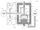
- FIG. 4shows a conceptual representation of another exemplary chemical-vapor-deposition system 400 incorporating teachings of the present invention.
- System 400includes a rectangular outer chamber 410 which encloses four deposition stations 420 , 422 , 424 , and 426 , loaded with respective substrates 200 , 202 , 204 , and 206 .
- each deposition stationis structurally and operationally analogous to system 100 in FIG. 1 .
- two or more of the stationsare operated in parallel.
- other embodiments of this multi-station systemarrange the stations in a cross formation, with each station confronting a respective lateral face of the chamber.
- Still other embodimentsuse different outer chamber geometries, for example cylindrical or spherical.
- One exemplary systemincludes an outer chamber, a substrate holder, and a unique gas-distribution fixture.
- the fixtureincludes a gas-distribution surface having holes for dispensing a gas and a gas-confinement member that engages, or otherwise cooperates with the substrate holder to form an inner chamber within the outer chamber.
- the inner chambernot only consumes less gas during deposition to reduce deposition waste and cost, but also facilitates rapid filling and evacuation to reduce deposition cycle times (with all other factors being equal.)
- the inner chamberalso places the gas-distribution fixture within several millimeters of a substrate on the substrate holder, promoting normal gas incidence across the chamber and thus uniform deposition thickness.
- One exemplary chemical-vapor deposition systemincludes an outer chamber, a substrate holder, and a unique gas-distribution fixture.
- the fixtureincludes a gas-distribution surface having holes for dispensing a gas and a gas-confinement member that forms a wall around the holes.
- the gas-confinement memberengages, or otherwise cooperates with the substrate holder to form an inner chamber within the outer chamber.
- the inner chamberhas a smaller volume than the outer chamber and thus consumes less gas during the deposition process than would the outer chamber used alone. Also, the smaller chamber volume allows the exhaust system to pump the chamber more quickly, thus increasing the rate of the CVD process.
- the exemplary showerheadis made of a material, like silicon, which can be easily passivated to reduce reaction with reactive gases, thus reducing chemical-vapor buildup in the showerhead. Also, the exemplary showerhead includes a configuration of holes that permits uniform gas flow.
Landscapes
- Chemical & Material Sciences (AREA)
- General Chemical & Material Sciences (AREA)
- Chemical Kinetics & Catalysis (AREA)
- Engineering & Computer Science (AREA)
- Materials Engineering (AREA)
- Mechanical Engineering (AREA)
- Metallurgy (AREA)
- Organic Chemistry (AREA)
- Chemical Vapour Deposition (AREA)
Abstract
Description
- This application is a Divisional of U.S. application Ser. No. 10/931,845, filed Aug. 31, 2004, which is a Divisional of U.S. application Ser. No. 09/797,324, filed Mar. 1, 2001, now U.S. Pat. No. 6,852,167, both of which are incorporated herein by reference.
- This invention concerns methods of making integrated circuits, particularly layer-formation, such as chemical-vapor deposition.
- Integrated circuits, the key components in thousands of electronic and computer products, are interconnected networks of electrical components fabricated on a common foundation, or substrate. Fabricators generally build these circuits layer by layer, using techniques, such as deposition, doping, masking, and etching, to form thousands and even millions of microscopic resistors, transistors, and other electrical components on a silicon substrate, known as a wafer. The components are then wired, or interconnected, together to define a specific electric circuit, such as a computer memory.
- One common technique for forming layers in an integrated circuit is called chemical vapor deposition. Chemical vapor deposition generally entails placing a substrate in a reaction chamber, heating the substrate to prescribed temperatures, and introducing one or more gases, known as precursor gases, into the chamber to begin a deposition cycle. The precursor gases enter the chamber through a gas-distribution fixture, such as a gas ring or a showerhead, one or more centimeters above the substrate, and descend toward the heated substrate. The gases react with each other and/or the heated substrate, blanketing its surface with a layer of material. An exhaust system then pumps gaseous by-products or leftovers from the reaction out of the chamber through a separate outlet to complete the deposition cycle.
- Conventional chemical-vapor-deposition (CVD) systems suffer from at least two problems. First, conventional CVD systems generally form layers that include microscopic hills and valleys and thus have non-uniform thickness. In the past, fabricators have been able to overcome these hills and valleys through use of post-deposition planarization or other compensation techniques. However, escalating demands for greater circuit density, for thinner layers, and for larger substrates make it increasingly difficult, if not completely impractical, to overcome the non-uniform thickness of conventional CVD layers.
- Second, some conventional CVD systems are also inefficient and time consuming. One significant factor affecting both CVD efficiency and duration is the size of conventional reaction chambers, which are generally made large to allow a loading mechanism to insert and extract the substrate. Large chambers generally require more gases to be introduced to achieve desired gas concentrations. However, much of this gas is not only unnecessary based on the amount of material deposited, but is typically treated as waste. Moreover, large chambers also take longer to fill up or pump out, prolonging deposition cycles and thus slowing fabrication of integrated circuits.
- Accordingly, there is a need for better systems and methods of chemical-vapor deposition.
FIG. 1 is a side view of an exemplary deposition reactor according to the invention;FIG. 2 is a top view of an exemplary gas-distribution fixture according to the invention;FIG. 3 is a flowchart showing an exemplary method according to the invention; andFIG. 4 is a diagram of anexemplary deposition system 400 incorporating a set of four deposition stations similar in structure and function tosystem 100 ofFIG. 1 .- The following detailed description, which references and incorporates
FIGS. 1-4 , describes and illustrates specific embodiments of the invention. These embodiments, offered not to limit but only to exemplify and teach the invention, are shown and described in sufficient detail to enable those skilled in the art to make and use the invention. Thus, where appropriate to avoid obscuring the invention, the description may omit certain information known to those of skill in the art. FIG. 1 shows an exemplary chemical-vapor-deposition system 100 which incorporates teachings of the present invention. In particular,system 100 includes achamber 110, awafer holder 120, a gas-distribution fixture 130, agas supply system 140, andexhaust pump 150, and aexhaust pump 160.- More particularly,
chamber 110 includes respective top andbottom plates sidewall 116. In the exemplary embodiment,chamber 110 is a cylindrical structure formed of stainless steel or glass. However, other embodiments use different structures and materials.Bottom plate 114 includes an opening114.1. Extending through opening114.1 is astem portion 122 ofwafer holder 120. Wafer holder 120 also includes asupport platform 124, one ormore heating elements 126, and one ormore temperature sensors 128.Support platform 124 supports one or more substrates, wafers, or integrated-circuit assemblies 200.Substrate 200 has an exemplary width or diameter of about 30 centimeters and an exemplary thickness in the range of 850-1000 microns. (The term “substrate,” as used herein, encompasses a semiconductor wafer as well as structures having one or more insulative, conductive, or semiconductive layers and materials. Thus, for example, the term embraces silicon-on-insulator, silicon-on-sapphire, and other advanced structures.)Heating elements 126 andtemperature sensors 128 are used forheating substrates 200 to a desired temperature.Holder 120 is coupled to a power supply and temperature control circuitry (both of which are not shown.) In the exemplary embodiment,wafer holder 120 is rotatable either manually or automatically and raises via manual or automatic lever mechanism (not shown). Abovewafer holder 120 andsubstrate 200 is gas-distribution fixture 130.- Fixture130 includes a gas-
distribution member 132, a surface-projection (or gas-confinement)member 134, and agas inlet 136. Gas inlet132 couples to gas-supply, gas-distribution channels 134, and agas inlet 136. In the exemplary embodiment,fixture 130 has two operating positions138.1 and138.2relative support platform 124. Fixture130 takes operating position138.1, before and after depositions and operating position138.2 during depositions. - Gas-
distribution member 132 includes gas-distribution holes, or orifices,132.1 and gas-distribution channels132.2. Holes132.1 define a gas-distribution surface132.3. In the exemplary embodiment, holes132.1 are substantially circular with a common diameter in the range of 15-20 microns; gas-distribution channels132.2 have a common width in the range of 20-45 microns; and surface132.3 is substantially planar and parallel to supportplatform 124 ofwafer holder 120. However, other embodiments use other surface forms as well as shapes and sizes of holes and channels. The distribution and size of holes may also affect deposition thickness and thus might be used to assist thickness control. Holes132.1 are coupled through gas-distribution channels132.2 togas inlet 136. - Surface-
projection member 134 projects or extends from surface132.3 towardsupport platform 124, defining a fixture cavity134.1. The exemplary embodiment forms surface-projection member 134 from stainless steel as a uniform annular or circular wall or collar that projects perpendicularly fromsurface 132 to define a right-cylindrical cavity. However, other embodiments formmember 134 to project at other angles relative surface132.3. For example, some form the projection at an acute or obtuse angle, such as 45 or 135 degrees, and others form the projection to peripherally define an oval, ellipse, triangle, square, or any desirable regular or irregular polygon. Thus, the present invention encompasses a wide variety of projection shapes and configurations, indeed any projection shape that facilitates definition of an effective cavity or gas-confinement volume in cooperation withwafer holder 120 and/orsubstrate 200. FIG. 2 , a plan view, shows further details of the exemplary embodiment of gas-distribution fixture 130. In particular, the plan view shows not only exemplary circular peripheries of gas-distribution member 132 and surface-projection member 134, but also an exemplary distribution pattern for holes132.1 and an exemplary orthogonal arrangement of gas-distribution channels132.2. Other embodiments, however, use other hole distribution patterns and channel arrangements. For example, some embodiments include random or concentric hole patterns and various channel geometries, including concentric circles, rectangles, or other regular or irregular concentric polygons. Some embodiments may also dedicate various subsets of channels and corresponding holes to different gases.- Gas-
distribution member 132 can be made in a number of ways. One exemplary method entails providing two wafers of materials, such as silicon or other passivatable, inert, or non-reactive material. One wafer is patterned and etched, for example, using conventional photolithographic or micro-electro-mechanical systems (MEMS) technology, to form a pattern holes, and the other wafer is patterned and etched to include a complementary or corresponding pattern of gas-distribution channels. (MEMS refers to the technologies of making structures and devices with micrometer dimensions.) Dry-etching techniques produce small openings and channels, while wet etching produces larger openings and channels. For further details, see, for example, M. Engelhardt, “Modern Application of Plasma Etching and Patterning in Silicon Process Technology, ” Contrib. Plasma Physics, vol. 39, no. 5, pp. 473-478(1999). - The two wafers are then bonded together with the holes and channels in appropriate alignment using known wafer-bonding techniques. See, for example, G. Krauter et al., “Room Temperature Silicon Wafer Bonding with Ultra-Thin Polymer Films, ” Advanced Materials, vol. 9, no. 5, pp. 417-420(1997); C.E. Hunt et al., “Direct Bonding of Micromachined Silicon Wafers for Laser Diode Heat Exchanger Applications, ” J. Micromech. Microeng, vol. 1, pp. 152-156(1991); Zucker, O. et al., “Applications of oxygen plasma processing to silicon direct bonding, ” Sensors and Actuators, A. Physical, vol. 36, no. 3, pp. 227-231(1993), which are all incorporated herein by reference. See also, copending and co-assigned U.S. patent application Ser. No. 09/189,276(dockets 303.534US1 and 97-1468) entitled “Low Temperature Silicon Wafer Bond Process with Bulk Material Bond Strength, ” which was filed Nov. 10, 1998 and which is also incorporated herein by reference. The resulting bonded structure is then passivated using thermal oxidation for example.
- For an alternative fixture structure and manufacturing method that can be combined with those of the exemplary embodiment, see U.S. Pat. No. 5,595,606, entitled “Shower Head and Film Forming Apparatus Using Same, which is incorporated herein by reference. In particular, one embodiment based on this patent adds a projection or gas-confinement member to the reported showerhead structure.
FIG. 1 also shows thatgas inlet 136 couples gas-distribution fixture 130 to gas-supply system 140. Gas-supply system 140 includes agas line 142,gas sources flow controllers conduit 142, which includes a flexible portion142.1, passes through an opening116.1 inchamber sidewall 116 to connect withgas inlet 136.Gas source 144 is coupled via mass-flow controller 146 togas line 142, andgas source 147 is coupled via mass-flow controller 147 togas line 142. The exemplary embodiment provides computer-controlled thermal or pressure-based mass-flow controllers; however, the invention is not limited to any particular number or type of mass-flow controller, nor to any particular number or set of gas sources.System 100 also includesvacuum pumps Vacuum pump 150 is coupled to gas-distribution fixture 130 via a mass-flow controller 152 andgas line 142. And,vacuum pump 160 is coupled to the interior ofchamber 110 via aline 162 and an opening114.2 inchamber bottom plate 114. In the exemplary embodiment,vacuum pump 160 has a greater capacity thanvacuum pump 150.- In general operation,
system 100 functions, via manual or automatic control, to move gas-distribution fixture 130 from operating position138.1 to position138.2, to introduce reactant gases throughfixture 130 ontosubstrate 200, and to deposit desired matter through chemical-vapor deposition onto the substrate. After the desired matter is deposited, pump150 evacuates gases throughfixture 130. - More particularly,
FIG. 3 shows aflowchart 300 which illustrates an exemplary method ofoperating system 100.Flowchart 300 includes process blocks202-216. - The exemplary method begins at
block 302 with insertion ofsubstrate 300 ontowafer holder 120. Execution then proceeds to block304. Block 304 establishes desired temperature and pressure conditions withinchamber 110. In the exemplary embodiment, this entails operatingheating element 126 to heatsubstrate 200 to a desired temperature, and operatingvacuum pump 160 to establish a desired pressure. Temperature and pressure are selected based on a number of factors, including composition of the substrate and reactant gases, as well as the desired reaction. After establishing these deposition conditions, execution continues atblock 306.- In
block 306, the system forms or closes an inner chamber aroundsubstrate 200, or more precisely a portion ofsubstrate 200 targeted for deposition. In the exemplary embodiment, this entails using a lever or other actuation mechanism (not shown) to move gas-distribution fixture 130 from position138.1 to position138.2 or to movewafer holder 120 from position138.2 to138.1. In either case, this movement places gas-distribution surface132.3 one-to-five millimeters from an upper most surface ofsubstrate 200. In this exemplary position, a lower-most surface of surface-projection member 134 contacts the upper surface ofsupport platform 124, with the inner chamber bounded by gas-distribution surface132.3, surface-projection member 134, and the upper surface ofsupport platform 124. - Other embodiments define in the inner chamber in other ways. For example, some embodiments include a surface-projection member on
support platform 124 ofwafer holder 120 to define a cavity analogous in structure and/or function to cavity134.1. In these embodiments, the surface-projection member takes the form of a vertical or slanted or curved wall, that extends fromsupport platform 124 and completely aroundsubstrate 200, and the gas-distribution fixture omits a surface-projection member. However, some embodiments include one or more surface-projection members on the gas-distribution fixture and the on the support platform, with the projection members on the fixture mating, engaging, or otherwise cooperating with those on the support platform to define a substantially or effectively closed chamber. In other words, the inner chamber need not be completely closed, but only sufficiently closed to facilitate a desired deposition. - After forming the inner chamber, the exemplary method continues at
block 308.Block 308 entails introducing one or more reactant or precursor gases into the separate chamber. To this end, the exemplary embodiment operates one or more mass-flow controllers, such ascontrollers sources gas line 142 andfixture 130 into the separate chamber. - Notably, the inner chamber is smaller in volume than
chamber 100 and thus requires less gas and less fill time to achieve desired chemical concentrations (assuming all other factors equal.) More precisely, the exemplary embodiment provides an inner chamber with an empty volume in the range of 70 to 350 cubic centimeters, based on a 1-to-5 millimeter inner-chamber height and a fixture with a 30-centimeter diameter. Additionally, the number and arrangement of holes in the fixture as well as the placement of the holes close to the substrate, for example within five millimeters of the substrate, promote normal gas incidence and uniform distribution of gases over the targeted portion ofsubstrate 200. Block 310 entails allowing the gases to react with each other and/or the heated substrate to deposit a layer of material on targeted portions of the substrate. It is expected that the resulting layer will exhibit a highly uniform thickness across the entire substrate because of the more uniform gas distribution.- Next, as
block 312 shows, the exemplary method entails evacuating gaseous waste or by-products produced during the deposition. To this end, the exemplary embodiment, activatesvacuum pump 160 to pump gaseous waste from the inner chamber through gas-distribution fixture 130. In some embodiments, pumps150 and160 are operated concurrently to establish initial pressure conditions and to evacuate the inner and outer chambers after deposition. - In
block 314, the system opens the separate chamber. In the exemplary embodiment, this entails automatically or manually moving gas-distribution fixture 130 to position138.1. Other embodiments, however, move the wafer holder or both the fixture and the wafer holder. Still other embodiments may use multipart collar or gas-confinement members which are moved laterally relative the wafer holder or gas-distribution fixture to open and close an inner chamber. - In
block 316,substrate 200 is unloaded fromchamber 110. Some embodiments remove the substrate manually, and others remove it using an automated wafer transport system. FIG. 4 shows a conceptual representation of another exemplary chemical-vapor-deposition system 400 incorporating teachings of the present invention.System 400 includes a rectangularouter chamber 410 which encloses fourdeposition stations respective substrates system 100 inFIG. 1 . In the exemplary embodiment, two or more of the stations are operated in parallel. Additionally, other embodiments of this multi-station system arrange the stations in a cross formation, with each station confronting a respective lateral face of the chamber. Still other embodiments use different outer chamber geometries, for example cylindrical or spherical.- In furtherance of the art, the inventor has presented new systems, methods, and apparatuses for chemical-vapor deposition. One exemplary system includes an outer chamber, a substrate holder, and a unique gas-distribution fixture. The fixture includes a gas-distribution surface having holes for dispensing a gas and a gas-confinement member that engages, or otherwise cooperates with the substrate holder to form an inner chamber within the outer chamber.
- Notably, the inner chamber not only consumes less gas during deposition to reduce deposition waste and cost, but also facilitates rapid filling and evacuation to reduce deposition cycle times (with all other factors being equal.) The inner chamber also places the gas-distribution fixture within several millimeters of a substrate on the substrate holder, promoting normal gas incidence across the chamber and thus uniform deposition thickness.
- To address these and other problems, the present inventor devised new systems, methods, and apparatuses for chemical-vapor deposition. One exemplary chemical-vapor deposition system includes an outer chamber, a substrate holder, and a unique gas-distribution fixture. The fixture includes a gas-distribution surface having holes for dispensing a gas and a gas-confinement member that forms a wall around the holes. In operation, the gas-confinement member engages, or otherwise cooperates with the substrate holder to form an inner chamber within the outer chamber.
- The inner chamber has a smaller volume than the outer chamber and thus consumes less gas during the deposition process than would the outer chamber used alone. Also, the smaller chamber volume allows the exhaust system to pump the chamber more quickly, thus increasing the rate of the CVD process. In addition, the exemplary showerhead is made of a material, like silicon, which can be easily passivated to reduce reaction with reactive gases, thus reducing chemical-vapor buildup in the showerhead. Also, the exemplary showerhead includes a configuration of holes that permits uniform gas flow.
- The embodiments described above are intended only to illustrate and teach one or more ways of practicing or implementing the present invention, not to restrict its breadth or scope. The actual scope of the invention, which embraces all ways of practicing or implementing the invention, is defined only by the following claims and their equivalents.
Claims (50)
1. A chemical-vapor deposition system comprising:
a first chamber for confining gases; and
a second chamber within the first chamber for at least partially containing a substrate during deposition.
2. The system ofclaim 1 , wherein the first chamber is a right cylindrical chamber.
3. The system ofclaim 1 , wherein the second chamber comprises a surface of a substrate-support structure.
4. The system ofclaim 3 , wherein the second chamber further comprises a gas-distribution fixture for atomic-layer deposition, the fixture confronting the surface of the substrate-support structure and comprising:
a non-reactive plate including a plurality of holes; and
a wall surrounding at least a portion of the plate.
5. The system ofclaim 1 , wherein the second chamber comprises one or more heating elements operable to heat the substrate, and one or more temperature sensors operable to monitor a temperature of the substrate.
6. The system ofclaim 1 , wherein the second chamber is configured to move relative to a position of the substrate.
7. The system ofclaim 1 , wherein the second chamber is fluidly coupled to a gas supply system.
8. The system ofclaim 7 , wherein the gas supply system comprises at least one reactant gas source, and a vacuum source.
9. The system ofclaim 1 , wherein the first chamber is coupled to a vacuum source.
10. A chemical-vapor deposition system comprising:
first means for confining one or more gases;
second means for confining one or more gases, the second means at least partly contained within the first means; and
third means for confining one or more gases, the third means at least partly contained within the first means.
11. The system ofclaim 10 , wherein the first means comprises a right cylindrical chamber.
12. The system ofclaim 10 , wherein the third means comprises a surface of a substrate-support structure.
13. The system ofclaim 10 , wherein the third means comprises one or more heating elements operable to heat a substrate positioned on the substrate-support structure, and one or more temperature sensors operable to monitor a temperature of the substrate.
14. The system ofclaim 10 , wherein the second means is separated from the third means by a gas distribution surface.
15. The system ofclaim 12 , wherein the third means comprises a surface projection member that cooperatively interacts with the substrate-support structure to form a gas confinement volume.
16. The system ofclaim 15 , wherein the surface projection member is configured to move relative to the substrate support structure.
17. The system ofclaim 10 , wherein the first means is fluidly coupled to a gas supply system.
18. The system ofclaim 17 , wherein the gas supply system comprises at least one reactant gas source, and a vacuum source.
19. The system ofclaim 10 , wherein the first means is coupled to a vacuum source.
20. A chemical-vapor deposition system comprising:
a first chamber for confining gases;
a second chamber within the first chamber configured to at least partially contain a substrate during deposition, the second chamber further comprising:
a first plate including one or more channels configured to communicate a gas flow; and
a second plate including two or more holes configured to communicate a gas flow, wherein the first and second plates are aligned to provide a continuous gas flow path from one of the channels to the holes.
21. The system ofclaim 20 , wherein at least one of the first plate and the second plate comprises silicon.
22. The system ofclaim 21 wherein the first plate and the second plate are photo lithographically patterned and etched to form the one or more channels and the two or more holes.
23. The system ofclaim 20 , wherein the first plate includes a plurality of channels orthogonally configured in the first plate.
24. The system ofclaim 20 , wherein the second plate comprises a hole arrangement in the second plate.
25. The system ofclaim 24 , wherein the hole arrangement includes one of a random arrangement of holes, a rectangular arrangement of holes, and a concentric arrangement of holes.
26. The system ofclaim 20 , wherein the second plate includes holes that range in diameter from approximately 15 microns to approximately 20 microns.
27. The system ofclaim 20 , wherein first plate includes channels that range in width from approximately 20 microns to approximately 45 microns.
28. The system ofclaim 20 , wherein the first plate and the second plate are fixedly aligned by bonding the first plate and the second plate.
29. The system ofclaim 28 , wherein bonding the first plate and the second plate comprises passivating the bonded structure using a thermal oxidation method.
30. The system ofclaim 20 , wherein the first plate comprises a gas inlet configured to fluidly communicate with the one or more channels.
31. The system ofclaim 30 , further comprising a gas supply system configured to fluidly communicate with the gas inlet.
32. A chemical-vapor deposition system comprising:
a first chamber for confining gases;
a second chamber within the first chamber to at least partially contain a substrate during a deposition process, the second chamber further comprising:
a first plate including at least one channel on a surface of the first plate and a gas inlet on an opposing surface that is configured to fluidly communicate with the at least one channel; and
a second plate including at least one aperture that extends through the second plate.
33. The system ofclaim 32 , wherein the first plate and the second plate sealably joined to provide a continuous flow passage that extends from the aperture to the gas inlet.
34. The system ofclaim 32 , wherein at least one of the first plate and the second plate comprises a silicon substrate.
35. The system ofclaim 32 , wherein the first plate and the second plate are photo lithographically patterned and etched to form the at least one channel and the at least one aperture.
36. The system ofclaim 32 , wherein the first plate includes a plurality of channels, wherein the plurality of channels are orthogonally positioned in the first plate.
37. The system ofclaim 32 , wherein the second plate includes a plurality of apertures, wherein the plurality of apertures comprises an aperture pattern in the second plate.
38. The system ofclaim 37 , wherein the aperture pattern includes one of a random pattern of apertures, a rectangular pattern of apertures, and a concentric pattern of apertures.
39. The system ofclaim 32 , wherein the second plate includes apertures that range in size from approximately 15 microns to approximately 20 microns.
40. The system ofclaim 32 , wherein first plate includes channels that range in width from approximately 20 microns to approximately 45 microns.
41. A chemical-vapor deposition system comprising:
a first chamber for confining gases;
a second chamber within the first chamber configured to at least partially contain a substrate during a deposition process, the second chamber further comprising:
a first plate including a plurality of channels on a surface, and a gas inlet on an opposing surface of the first plate that is configured to fluidly communicate with the plurality of channels;
a second plate including a plurality of apertures that extend through the second plate, the first plate and the second plate being sealably joined to provide a continuous flow passage that extends from the apertures to the gas inlet.
42. The system ofclaim 41 , wherein the plurality of channels comprise channels having a common width that ranges between approximately 20 microns and approximately 45 microns.
43. The system ofclaim 41 , wherein the plurality of apertures comprise apertures having a common diameter that ranges between approximately 15 microns and approximately 20 microns.
44. The system ofclaim 41 , wherein the plurality of apertures comprise a random arrangement of the apertures in the second plate.
45. The system ofclaim 41 , wherein the plurality of apertures comprise a circular arrangement of the apertures in the second plate.
46. The system ofclaim 41 , wherein the plurality of apertures comprise a rectangular arrangement of the apertures in the second plate.
47. The system ofclaim 41 , wherein the plurality of channels comprise an orthogonal arrangement of the channels.
48. The system ofclaim 41 , wherein the plurality of channels comprise a concentric circular arrangement of the channels.
49. The system ofclaim 41 , wherein the first plate and the second plate are sealably joined by bonding the first plate and the second plate using a silicon wafer bonding method to form a bonded structure.
50. The system ofclaim 49 , wherein the bonded structure comprises a passivated and bonded structure.
Priority Applications (1)
| Application Number | Priority Date | Filing Date | Title |
|---|---|---|---|
| US11/651,136US20070107661A1 (en) | 2001-03-01 | 2007-01-09 | Methods, systems, and apparatus for uniform chemical-vapor depositions |
Applications Claiming Priority (3)
| Application Number | Priority Date | Filing Date | Title |
|---|---|---|---|
| US09/797,324US6852167B2 (en) | 2001-03-01 | 2001-03-01 | Methods, systems, and apparatus for uniform chemical-vapor depositions |
| US10/931,845US20050087134A1 (en) | 2001-03-01 | 2004-08-31 | Methods, systems, and apparatus for uniform chemical-vapor depositions |
| US11/651,136US20070107661A1 (en) | 2001-03-01 | 2007-01-09 | Methods, systems, and apparatus for uniform chemical-vapor depositions |
Related Parent Applications (1)
| Application Number | Title | Priority Date | Filing Date |
|---|---|---|---|
| US10/931,845DivisionUS20050087134A1 (en) | 2001-03-01 | 2004-08-31 | Methods, systems, and apparatus for uniform chemical-vapor depositions |
Publications (1)
| Publication Number | Publication Date |
|---|---|
| US20070107661A1true US20070107661A1 (en) | 2007-05-17 |
Family
ID=25170514
Family Applications (5)
| Application Number | Title | Priority Date | Filing Date |
|---|---|---|---|
| US09/797,324Expired - Fee RelatedUS6852167B2 (en) | 2001-03-01 | 2001-03-01 | Methods, systems, and apparatus for uniform chemical-vapor depositions |
| US10/931,595Expired - Fee RelatedUS7410668B2 (en) | 2001-03-01 | 2004-08-31 | Methods, systems, and apparatus for uniform chemical-vapor depositions |
| US10/931,845AbandonedUS20050087134A1 (en) | 2001-03-01 | 2004-08-31 | Methods, systems, and apparatus for uniform chemical-vapor depositions |
| US11/651,295AbandonedUS20070131169A1 (en) | 2001-03-01 | 2007-01-09 | Methods, systems, and apparatus for uniform chemical-vapor depositions |
| US11/651,136AbandonedUS20070107661A1 (en) | 2001-03-01 | 2007-01-09 | Methods, systems, and apparatus for uniform chemical-vapor depositions |
Family Applications Before (4)
| Application Number | Title | Priority Date | Filing Date |
|---|---|---|---|
| US09/797,324Expired - Fee RelatedUS6852167B2 (en) | 2001-03-01 | 2001-03-01 | Methods, systems, and apparatus for uniform chemical-vapor depositions |
| US10/931,595Expired - Fee RelatedUS7410668B2 (en) | 2001-03-01 | 2004-08-31 | Methods, systems, and apparatus for uniform chemical-vapor depositions |
| US10/931,845AbandonedUS20050087134A1 (en) | 2001-03-01 | 2004-08-31 | Methods, systems, and apparatus for uniform chemical-vapor depositions |
| US11/651,295AbandonedUS20070131169A1 (en) | 2001-03-01 | 2007-01-09 | Methods, systems, and apparatus for uniform chemical-vapor depositions |
Country Status (1)
| Country | Link |
|---|---|
| US (5) | US6852167B2 (en) |
Cited By (21)
| Publication number | Priority date | Publication date | Assignee | Title |
|---|---|---|---|---|
| US7326980B2 (en) | 2002-08-28 | 2008-02-05 | Micron Technology, Inc. | Devices with HfSiON dielectric films which are Hf-O rich |
| US7388246B2 (en) | 2002-08-29 | 2008-06-17 | Micron Technology, Inc. | Lanthanide doped TiOx dielectric films |
| US7402876B2 (en) | 2002-12-04 | 2008-07-22 | Micron Technology, Inc. | Zr— Sn—Ti—O films |
| US7405454B2 (en) | 2003-03-04 | 2008-07-29 | Micron Technology, Inc. | Electronic apparatus with deposited dielectric layers |
| US7410668B2 (en) | 2001-03-01 | 2008-08-12 | Micron Technology, Inc. | Methods, systems, and apparatus for uniform chemical-vapor depositions |
| US7439194B2 (en) | 2002-08-15 | 2008-10-21 | Micron Technology, Inc. | Lanthanide doped TiOx dielectric films by plasma oxidation |
| US7554161B2 (en) | 2002-06-05 | 2009-06-30 | Micron Technology, Inc. | HfAlO3 films for gate dielectrics |
| US7560395B2 (en) | 2005-01-05 | 2009-07-14 | Micron Technology, Inc. | Atomic layer deposited hafnium tantalum oxide dielectrics |
| US7588988B2 (en) | 2004-08-31 | 2009-09-15 | Micron Technology, Inc. | Method of forming apparatus having oxide films formed using atomic layer deposition |
| US7601649B2 (en) | 2004-08-02 | 2009-10-13 | Micron Technology, Inc. | Zirconium-doped tantalum oxide films |
| US7605030B2 (en) | 2006-08-31 | 2009-10-20 | Micron Technology, Inc. | Hafnium tantalum oxynitride high-k dielectric and metal gates |
| US7611959B2 (en) | 2002-12-04 | 2009-11-03 | Micron Technology, Inc. | Zr-Sn-Ti-O films |
| US7625794B2 (en) | 2003-03-31 | 2009-12-01 | Micron Technology, Inc. | Methods of forming zirconium aluminum oxide |
| US7662729B2 (en) | 2005-04-28 | 2010-02-16 | Micron Technology, Inc. | Atomic layer deposition of a ruthenium layer to a lanthanide oxide dielectric layer |
| US7670646B2 (en) | 2002-05-02 | 2010-03-02 | Micron Technology, Inc. | Methods for atomic-layer deposition |
| US7709402B2 (en) | 2006-02-16 | 2010-05-04 | Micron Technology, Inc. | Conductive layers for hafnium silicon oxynitride films |
| US7719065B2 (en) | 2004-08-26 | 2010-05-18 | Micron Technology, Inc. | Ruthenium layer for a dielectric layer containing a lanthanide oxide |
| US7867919B2 (en) | 2004-08-31 | 2011-01-11 | Micron Technology, Inc. | Method of fabricating an apparatus having a lanthanum-metal oxide dielectric layer |
| US20110305836A1 (en)* | 2009-03-10 | 2011-12-15 | Mitsui Engineering & Shipbuilding Co., Ltd. | Atomic layer deposition apparatus and thin film forming method |
| US9175393B1 (en)* | 2011-08-31 | 2015-11-03 | Alta Devices, Inc. | Tiled showerhead for a semiconductor chemical vapor deposition reactor |
| US10066297B2 (en)* | 2011-08-31 | 2018-09-04 | Alta Devices, Inc. | Tiled showerhead for a semiconductor chemical vapor deposition reactor |
Families Citing this family (430)
| Publication number | Priority date | Publication date | Assignee | Title |
|---|---|---|---|---|
| US6828292B2 (en)* | 2000-06-05 | 2004-12-07 | Procter & Gamble Company | Domestic fabric article refreshment in integrated cleaning and treatment processes |
| JP3667202B2 (en)* | 2000-07-13 | 2005-07-06 | 株式会社荏原製作所 | Substrate processing equipment |
| JP3886424B2 (en)* | 2001-08-28 | 2007-02-28 | 鹿児島日本電気株式会社 | Substrate processing apparatus and method |
| US7476925B2 (en)* | 2001-08-30 | 2009-01-13 | Micron Technology, Inc. | Atomic layer deposition of metal oxide and/or low asymmetrical tunnel barrier interploy insulators |
| US6844203B2 (en) | 2001-08-30 | 2005-01-18 | Micron Technology, Inc. | Gate oxides, and methods of forming |
| KR100782529B1 (en)* | 2001-11-08 | 2007-12-06 | 에이에스엠지니텍코리아 주식회사 | Deposition equipment |
| US6893506B2 (en) | 2002-03-11 | 2005-05-17 | Micron Technology, Inc. | Atomic layer deposition apparatus and method |
| US7589029B2 (en) | 2002-05-02 | 2009-09-15 | Micron Technology, Inc. | Atomic layer deposition and conversion |
| US7045430B2 (en)* | 2002-05-02 | 2006-05-16 | Micron Technology Inc. | Atomic layer-deposited LaAlO3 films for gate dielectrics |
| US7205218B2 (en)* | 2002-06-05 | 2007-04-17 | Micron Technology, Inc. | Method including forming gate dielectrics having multiple lanthanide oxide layers |
| US7217336B2 (en)* | 2002-06-20 | 2007-05-15 | Tokyo Electron Limited | Directed gas injection apparatus for semiconductor processing |
| US7221586B2 (en) | 2002-07-08 | 2007-05-22 | Micron Technology, Inc. | Memory utilizing oxide nanolaminates |
| US6921702B2 (en)* | 2002-07-30 | 2005-07-26 | Micron Technology Inc. | Atomic layer deposited nanolaminates of HfO2/ZrO2 films as gate dielectrics |
| JP2005536042A (en)* | 2002-08-08 | 2005-11-24 | トリコン テクノロジーズ リミティド | Improved shower head |
| US6790791B2 (en) | 2002-08-15 | 2004-09-14 | Micron Technology, Inc. | Lanthanide doped TiOx dielectric films |
| US7037863B2 (en)* | 2002-09-10 | 2006-05-02 | Samsung Electronics Co., Ltd. | Post thermal treatment methods of forming high dielectric layers over interfacial layers in integrated circuit devices |
| US6784096B2 (en) | 2002-09-11 | 2004-08-31 | Applied Materials, Inc. | Methods and apparatus for forming barrier layers in high aspect ratio vias |
| DE10243022A1 (en)* | 2002-09-17 | 2004-03-25 | Degussa Ag | Separation of a solid by thermal decomposition of a gaseous substance in a cup reactor |
| JP4113755B2 (en)* | 2002-10-03 | 2008-07-09 | 東京エレクトロン株式会社 | Processing equipment |
| KR20110118735A (en)* | 2003-03-17 | 2011-10-31 | 시그마-알드리치컴퍼니 | Precursor for Metal Oxide Layer or Metal Oxide Film Deposition |
| US7183186B2 (en) | 2003-04-22 | 2007-02-27 | Micro Technology, Inc. | Atomic layer deposited ZrTiO4 films |
| US7049192B2 (en) | 2003-06-24 | 2006-05-23 | Micron Technology, Inc. | Lanthanide oxide / hafnium oxide dielectrics |
| US7192824B2 (en) | 2003-06-24 | 2007-03-20 | Micron Technology, Inc. | Lanthanide oxide / hafnium oxide dielectric layers |
| US20050103265A1 (en)* | 2003-11-19 | 2005-05-19 | Applied Materials, Inc., A Delaware Corporation | Gas distribution showerhead featuring exhaust apertures |
| JP4399517B2 (en)* | 2004-01-05 | 2010-01-20 | 株式会社堀場製作所 | Film forming apparatus and film forming method |
| US7326293B2 (en)* | 2004-03-26 | 2008-02-05 | Zyvex Labs, Llc | Patterned atomic layer epitaxy |
| US20050221618A1 (en)* | 2004-03-31 | 2005-10-06 | Amrhein Frederick J | System for controlling a plenum output flow geometry |
| US20050223983A1 (en)* | 2004-04-08 | 2005-10-13 | Venkat Selvamanickam | Chemical vapor deposition (CVD) apparatus usable in the manufacture of superconducting conductors |
| US20050268848A1 (en)* | 2004-04-28 | 2005-12-08 | Nanodynamics, Inc | Atomic layer deposition apparatus and process |
| JP4879509B2 (en)* | 2004-05-21 | 2012-02-22 | 株式会社アルバック | Vacuum deposition system |
| US20060073276A1 (en)* | 2004-10-04 | 2006-04-06 | Eric Antonissen | Multi-zone atomic layer deposition apparatus and method |
| US7238623B2 (en)* | 2004-10-06 | 2007-07-03 | Texas Instruments Incorporated | Versatile system for self-aligning deposition equipment |
| US7235501B2 (en) | 2004-12-13 | 2007-06-26 | Micron Technology, Inc. | Lanthanum hafnium oxide dielectrics |
| US20060125030A1 (en)* | 2004-12-13 | 2006-06-15 | Micron Technology, Inc. | Hybrid ALD-CVD of PrxOy/ZrO2 films as gate dielectrics |
| US7374964B2 (en) | 2005-02-10 | 2008-05-20 | Micron Technology, Inc. | Atomic layer deposition of CeO2/Al2O3 films as gate dielectrics |
| US7480974B2 (en)* | 2005-02-15 | 2009-01-27 | Lam Research Corporation | Methods of making gas distribution members for plasma processing apparatuses |
| CN101128622B (en)* | 2005-02-22 | 2010-08-25 | 埃克提斯公司 | Etching chamber with subchamber |
| US7687409B2 (en) | 2005-03-29 | 2010-03-30 | Micron Technology, Inc. | Atomic layer deposited titanium silicon oxide films |
| US7365027B2 (en)* | 2005-03-29 | 2008-04-29 | Micron Technology, Inc. | ALD of amorphous lanthanide doped TiOx films |
| US7390756B2 (en) | 2005-04-28 | 2008-06-24 | Micron Technology, Inc. | Atomic layer deposited zirconium silicon oxide films |
| JP2008540840A (en)* | 2005-05-09 | 2008-11-20 | エイエスエム・ジェニテック・コリア・リミテッド | Reactor of atomic layer deposition apparatus with multiple gas inlets |
| GB0510051D0 (en)* | 2005-05-17 | 2005-06-22 | Forticrete Ltd | Interlocking roof tiles |
| US7572695B2 (en) | 2005-05-27 | 2009-08-11 | Micron Technology, Inc. | Hafnium titanium oxide films |
| US7927948B2 (en) | 2005-07-20 | 2011-04-19 | Micron Technology, Inc. | Devices with nanocrystals and methods of formation |
| US20070049023A1 (en)* | 2005-08-29 | 2007-03-01 | Micron Technology, Inc. | Zirconium-doped gadolinium oxide films |
| US8110469B2 (en)* | 2005-08-30 | 2012-02-07 | Micron Technology, Inc. | Graded dielectric layers |
| US8071476B2 (en) | 2005-08-31 | 2011-12-06 | Micron Technology, Inc. | Cobalt titanium oxide dielectric films |
| US7410910B2 (en) | 2005-08-31 | 2008-08-12 | Micron Technology, Inc. | Lanthanum aluminum oxynitride dielectric films |
| US8471254B2 (en)* | 2005-12-27 | 2013-06-25 | Hana Microdisplay Technologies, Inc. | Liquid crystal cells with uniform cell gap and methods of manufacture |
| US20070169687A1 (en)* | 2006-01-26 | 2007-07-26 | Caracal, Inc. | Silicon carbide formation by alternating pulses |
| US7670432B2 (en)* | 2006-03-08 | 2010-03-02 | Tokyo Electron Limited | Exhaust system for a vacuum processing system |
| US7794546B2 (en)* | 2006-03-08 | 2010-09-14 | Tokyo Electron Limited | Sealing device and method for a processing system |
| US20070218702A1 (en)* | 2006-03-15 | 2007-09-20 | Asm Japan K.K. | Semiconductor-processing apparatus with rotating susceptor |
| US7737500B2 (en)* | 2006-04-26 | 2010-06-15 | International Business Machines Corporation | CMOS diodes with dual gate conductors, and methods for forming the same |
| KR20080027009A (en)* | 2006-09-22 | 2008-03-26 | 에이에스엠지니텍코리아 주식회사 | Atomic layer deposition apparatus and multilayer film deposition method using the same |
| CN101517475B (en)* | 2006-09-26 | 2012-09-05 | 南京长青激光科技有限责任公司 | Method and device for fabricating domain inversion structure on nonlinear ferroelectric substrate |
| US8715455B2 (en)* | 2007-02-06 | 2014-05-06 | Tokyo Electron Limited | Multi-zone gas distribution system for a treatment system |
| US7435636B1 (en) | 2007-03-29 | 2008-10-14 | Micron Technology, Inc. | Fabrication of self-aligned gallium arsenide MOSFETs using damascene gate methods |
| US20080241384A1 (en)* | 2007-04-02 | 2008-10-02 | Asm Genitech Korea Ltd. | Lateral flow deposition apparatus and method of depositing film by using the apparatus |
| US7671394B2 (en)* | 2007-10-17 | 2010-03-02 | International Business Machines Corporation | Embedded trench capacitor having a high-k node dielectric and a metallic inner electrode |
| US8282735B2 (en)* | 2007-11-27 | 2012-10-09 | Asm Genitech Korea Ltd. | Atomic layer deposition apparatus |
| US7728392B2 (en)* | 2008-01-03 | 2010-06-01 | International Business Machines Corporation | SRAM device structure including same band gap transistors having gate stacks with high-K dielectrics and same work function |
| US7879183B2 (en)* | 2008-02-27 | 2011-02-01 | Applied Materials, Inc. | Apparatus and method for front side protection during backside cleaning |
| US8273178B2 (en) | 2008-02-28 | 2012-09-25 | Asm Genitech Korea Ltd. | Thin film deposition apparatus and method of maintaining the same |
| US8159040B2 (en) | 2008-05-13 | 2012-04-17 | International Business Machines Corporation | Metal gate integration structure and method including metal fuse, anti-fuse and/or resistor |
| TWI467045B (en)* | 2008-05-23 | 2015-01-01 | Sigma Aldrich Co | High-k dielectric films and methods of producing high-k dielectric films using cerium-based precursors |
| TW200949939A (en)* | 2008-05-23 | 2009-12-01 | Sigma Aldrich Co | High-k dielectric films and methods of producing using titanium-based β -diketonate precursors |
| US8089135B2 (en)* | 2008-07-30 | 2012-01-03 | International Business Machine Corporation | Back-end-of-line wiring structures with integrated passive elements and design structures for a radiofrequency integrated circuit |
| US8216376B1 (en)* | 2009-01-15 | 2012-07-10 | Intermolecular, Inc. | Method and apparatus for variable conductance |
| US9394608B2 (en) | 2009-04-06 | 2016-07-19 | Asm America, Inc. | Semiconductor processing reactor and components thereof |
| US8222104B2 (en) | 2009-07-27 | 2012-07-17 | International Business Machines Corporation | Three dimensional integrated deep trench decoupling capacitors |
| US8802201B2 (en) | 2009-08-14 | 2014-08-12 | Asm America, Inc. | Systems and methods for thin-film deposition of metal oxides using excited nitrogen-oxygen species |
| US9920418B1 (en) | 2010-09-27 | 2018-03-20 | James Stabile | Physical vapor deposition apparatus having a tapered chamber |
| US20120180725A1 (en)* | 2011-01-17 | 2012-07-19 | Furukawa Electric Co., Ltd. | Cvd apparatus |
| US20130023129A1 (en) | 2011-07-20 | 2013-01-24 | Asm America, Inc. | Pressure transmitter for a semiconductor processing environment |
| US8525339B2 (en) | 2011-07-27 | 2013-09-03 | International Business Machines Corporation | Hybrid copper interconnect structure and method of fabricating same |
| US9017481B1 (en) | 2011-10-28 | 2015-04-28 | Asm America, Inc. | Process feed management for semiconductor substrate processing |
| JP5541274B2 (en)* | 2011-12-28 | 2014-07-09 | 東京エレクトロン株式会社 | Substrate processing apparatus, substrate processing method, and storage medium |
| US9679751B2 (en) | 2012-03-15 | 2017-06-13 | Lam Research Corporation | Chamber filler kit for plasma etch chamber useful for fast gas switching |
| KR101881894B1 (en)* | 2012-04-06 | 2018-07-26 | 삼성디스플레이 주식회사 | Thin film depositing apparatus and the thin film depositing method using the same |
| US20130333616A1 (en)* | 2012-06-18 | 2013-12-19 | Tel Solar Ag | Plasma processing system with movable chamber housing parts |
| US10227939B2 (en) | 2012-08-24 | 2019-03-12 | GM Global Technology Operations LLC | Cylinder deactivation pattern matching |
| US9726139B2 (en) | 2012-09-10 | 2017-08-08 | GM Global Technology Operations LLC | System and method for controlling a firing sequence of an engine to reduce vibration when cylinders of the engine are deactivated |
| US9458779B2 (en) | 2013-01-07 | 2016-10-04 | GM Global Technology Operations LLC | Intake runner temperature determination systems and methods |
| US9458778B2 (en) | 2012-08-24 | 2016-10-04 | GM Global Technology Operations LLC | Cylinder activation and deactivation control systems and methods |
| US9416743B2 (en) | 2012-10-03 | 2016-08-16 | GM Global Technology Operations LLC | Cylinder activation/deactivation sequence control systems and methods |
| US9638121B2 (en)* | 2012-08-24 | 2017-05-02 | GM Global Technology Operations LLC | System and method for deactivating a cylinder of an engine and reactivating the cylinder based on an estimated trapped air mass |
| US9650978B2 (en) | 2013-01-07 | 2017-05-16 | GM Global Technology Operations LLC | System and method for randomly adjusting a firing frequency of an engine to reduce vibration when cylinders of the engine are deactivated |
| US9382853B2 (en) | 2013-01-22 | 2016-07-05 | GM Global Technology Operations LLC | Cylinder control systems and methods for discouraging resonant frequency operation |
| US9376973B2 (en) | 2012-09-10 | 2016-06-28 | GM Global Technology Operations LLC | Volumetric efficiency determination systems and methods |
| US9534550B2 (en) | 2012-09-10 | 2017-01-03 | GM Global Technology Operations LLC | Air per cylinder determination systems and methods |
| US9458780B2 (en) | 2012-09-10 | 2016-10-04 | GM Global Technology Operations LLC | Systems and methods for controlling cylinder deactivation periods and patterns |
| US9719439B2 (en) | 2012-08-24 | 2017-08-01 | GM Global Technology Operations LLC | System and method for controlling spark timing when cylinders of an engine are deactivated to reduce noise and vibration |
| US10714315B2 (en) | 2012-10-12 | 2020-07-14 | Asm Ip Holdings B.V. | Semiconductor reaction chamber showerhead |
| US9175389B2 (en)* | 2012-12-21 | 2015-11-03 | Intermolecular, Inc. | ALD process window combinatorial screening tool |
| US9312203B2 (en) | 2013-01-02 | 2016-04-12 | Globalfoundries Inc. | Dual damascene structure with liner |
| US20160376700A1 (en) | 2013-02-01 | 2016-12-29 | Asm Ip Holding B.V. | System for treatment of deposition reactor |
| US9494092B2 (en) | 2013-03-13 | 2016-11-15 | GM Global Technology Operations LLC | System and method for predicting parameters associated with airflow through an engine |
| US9741918B2 (en) | 2013-10-07 | 2017-08-22 | Hypres, Inc. | Method for increasing the integration level of superconducting electronics circuits, and a resulting circuit |
| US11015245B2 (en) | 2014-03-19 | 2021-05-25 | Asm Ip Holding B.V. | Gas-phase reactor and system having exhaust plenum and components thereof |
| US10077497B2 (en)* | 2014-05-30 | 2018-09-18 | Lam Research Corporation | Hollow cathode discharge (HCD) suppressing capacitively coupled plasma electrode and gas distribution faceplate |
| US9441550B2 (en) | 2014-06-10 | 2016-09-13 | GM Global Technology Operations LLC | Cylinder firing fraction determination and control systems and methods |
| US9341128B2 (en) | 2014-06-12 | 2016-05-17 | GM Global Technology Operations LLC | Fuel consumption based cylinder activation and deactivation control systems and methods |
| US9556811B2 (en) | 2014-06-20 | 2017-01-31 | GM Global Technology Operations LLC | Firing pattern management for improved transient vibration in variable cylinder deactivation mode |
| US10858737B2 (en) | 2014-07-28 | 2020-12-08 | Asm Ip Holding B.V. | Showerhead assembly and components thereof |
| US9890456B2 (en) | 2014-08-21 | 2018-02-13 | Asm Ip Holding B.V. | Method and system for in situ formation of gas-phase compounds |
| US10941490B2 (en) | 2014-10-07 | 2021-03-09 | Asm Ip Holding B.V. | Multiple temperature range susceptor, assembly, reactor and system including the susceptor, and methods of using the same |
| US9599047B2 (en) | 2014-11-20 | 2017-03-21 | GM Global Technology Operations LLC | Combination cylinder state and transmission gear control systems and methods |
| JP6354539B2 (en)* | 2014-11-25 | 2018-07-11 | 東京エレクトロン株式会社 | Substrate processing apparatus, substrate processing method, and storage medium |
| US10276355B2 (en) | 2015-03-12 | 2019-04-30 | Asm Ip Holding B.V. | Multi-zone reactor, system including the reactor, and method of using the same |
| JP6050860B1 (en)* | 2015-05-26 | 2016-12-21 | 株式会社日本製鋼所 | Plasma atomic layer growth equipment |
| JP6054471B2 (en) | 2015-05-26 | 2016-12-27 | 株式会社日本製鋼所 | Atomic layer growth apparatus and exhaust layer of atomic layer growth apparatus |
| JP6054470B2 (en) | 2015-05-26 | 2016-12-27 | 株式会社日本製鋼所 | Atomic layer growth equipment |
| US10337441B2 (en) | 2015-06-09 | 2019-07-02 | GM Global Technology Operations LLC | Air per cylinder determination systems and methods |
| US10458018B2 (en) | 2015-06-26 | 2019-10-29 | Asm Ip Holding B.V. | Structures including metal carbide material, devices including the structures, and methods of forming same |
| US10403515B2 (en)* | 2015-09-24 | 2019-09-03 | Applied Materials, Inc. | Loadlock integrated bevel etcher system |
| US10211308B2 (en) | 2015-10-21 | 2019-02-19 | Asm Ip Holding B.V. | NbMC layers |
| US10358721B2 (en)* | 2015-10-22 | 2019-07-23 | Asm Ip Holding B.V. | Semiconductor manufacturing system including deposition apparatus |
| US11139308B2 (en) | 2015-12-29 | 2021-10-05 | Asm Ip Holding B.V. | Atomic layer deposition of III-V compounds to form V-NAND devices |
| AT517608B1 (en)* | 2016-01-21 | 2017-03-15 | Avl List Gmbh | Electronic unit for a flowmeter |
| US10529554B2 (en) | 2016-02-19 | 2020-01-07 | Asm Ip Holding B.V. | Method for forming silicon nitride film selectively on sidewalls or flat surfaces of trenches |
| US10343920B2 (en) | 2016-03-18 | 2019-07-09 | Asm Ip Holding B.V. | Aligned carbon nanotubes |
| US10865475B2 (en) | 2016-04-21 | 2020-12-15 | Asm Ip Holding B.V. | Deposition of metal borides and silicides |
| US10190213B2 (en) | 2016-04-21 | 2019-01-29 | Asm Ip Holding B.V. | Deposition of metal borides |
| US10367080B2 (en) | 2016-05-02 | 2019-07-30 | Asm Ip Holding B.V. | Method of forming a germanium oxynitride film |
| US11453943B2 (en) | 2016-05-25 | 2022-09-27 | Asm Ip Holding B.V. | Method for forming carbon-containing silicon/metal oxide or nitride film by ALD using silicon precursor and hydrocarbon precursor |
| JP6756853B2 (en)* | 2016-06-03 | 2020-09-16 | アプライド マテリアルズ インコーポレイテッドApplied Materials,Incorporated | Effective and new design for low particle count and better wafer quality by diffusing the flow inside the chamber |
| US9859151B1 (en) | 2016-07-08 | 2018-01-02 | Asm Ip Holding B.V. | Selective film deposition method to form air gaps |
| US10612137B2 (en) | 2016-07-08 | 2020-04-07 | Asm Ip Holdings B.V. | Organic reactants for atomic layer deposition |
| US9812320B1 (en) | 2016-07-28 | 2017-11-07 | Asm Ip Holding B.V. | Method and apparatus for filling a gap |
| US9887082B1 (en) | 2016-07-28 | 2018-02-06 | Asm Ip Holding B.V. | Method and apparatus for filling a gap |
| KR102532607B1 (en) | 2016-07-28 | 2023-05-15 | 에이에스엠 아이피 홀딩 비.브이. | Substrate processing apparatus and method of operating the same |
| US10643826B2 (en) | 2016-10-26 | 2020-05-05 | Asm Ip Holdings B.V. | Methods for thermally calibrating reaction chambers |
| US11532757B2 (en) | 2016-10-27 | 2022-12-20 | Asm Ip Holding B.V. | Deposition of charge trapping layers |
| US10714350B2 (en) | 2016-11-01 | 2020-07-14 | ASM IP Holdings, B.V. | Methods for forming a transition metal niobium nitride film on a substrate by atomic layer deposition and related semiconductor device structures |
| US10229833B2 (en) | 2016-11-01 | 2019-03-12 | Asm Ip Holding B.V. | Methods for forming a transition metal nitride film on a substrate by atomic layer deposition and related semiconductor device structures |
| KR102546317B1 (en) | 2016-11-15 | 2023-06-21 | 에이에스엠 아이피 홀딩 비.브이. | Gas supply unit and substrate processing apparatus including the same |
| KR102762543B1 (en) | 2016-12-14 | 2025-02-05 | 에이에스엠 아이피 홀딩 비.브이. | Substrate processing apparatus |
| US11581186B2 (en) | 2016-12-15 | 2023-02-14 | Asm Ip Holding B.V. | Sequential infiltration synthesis apparatus |
| US11447861B2 (en) | 2016-12-15 | 2022-09-20 | Asm Ip Holding B.V. | Sequential infiltration synthesis apparatus and a method of forming a patterned structure |
| KR102700194B1 (en)* | 2016-12-19 | 2024-08-28 | 에이에스엠 아이피 홀딩 비.브이. | Substrate processing apparatus |
| US10269558B2 (en) | 2016-12-22 | 2019-04-23 | Asm Ip Holding B.V. | Method of forming a structure on a substrate |
| US10867788B2 (en) | 2016-12-28 | 2020-12-15 | Asm Ip Holding B.V. | Method of forming a structure on a substrate |
| US11390950B2 (en) | 2017-01-10 | 2022-07-19 | Asm Ip Holding B.V. | Reactor system and method to reduce residue buildup during a film deposition process |
| US10468261B2 (en) | 2017-02-15 | 2019-11-05 | Asm Ip Holding B.V. | Methods for forming a metallic film on a substrate by cyclical deposition and related semiconductor device structures |
| US10224224B2 (en)* | 2017-03-10 | 2019-03-05 | Micromaterials, LLC | High pressure wafer processing systems and related methods |
| US10529563B2 (en) | 2017-03-29 | 2020-01-07 | Asm Ip Holdings B.V. | Method for forming doped metal oxide films on a substrate by cyclical deposition and related semiconductor device structures |
| KR102457289B1 (en) | 2017-04-25 | 2022-10-21 | 에이에스엠 아이피 홀딩 비.브이. | Method for depositing a thin film and manufacturing a semiconductor device |
| US10892156B2 (en) | 2017-05-08 | 2021-01-12 | Asm Ip Holding B.V. | Methods for forming a silicon nitride film on a substrate and related semiconductor device structures |
| US10770286B2 (en) | 2017-05-08 | 2020-09-08 | Asm Ip Holdings B.V. | Methods for selectively forming a silicon nitride film on a substrate and related semiconductor device structures |
| US10622214B2 (en) | 2017-05-25 | 2020-04-14 | Applied Materials, Inc. | Tungsten defluorination by high pressure treatment |
| US10886123B2 (en) | 2017-06-02 | 2021-01-05 | Asm Ip Holding B.V. | Methods for forming low temperature semiconductor layers and related semiconductor device structures |
| CN110678973B (en) | 2017-06-02 | 2023-09-19 | 应用材料公司 | Dry stripping of boron carbide hard masks |
| US12040200B2 (en) | 2017-06-20 | 2024-07-16 | Asm Ip Holding B.V. | Semiconductor processing apparatus and methods for calibrating a semiconductor processing apparatus |
| US11851763B2 (en)* | 2017-06-23 | 2023-12-26 | General Electric Company | Chemical vapor deposition during additive manufacturing |
| US11306395B2 (en) | 2017-06-28 | 2022-04-19 | Asm Ip Holding B.V. | Methods for depositing a transition metal nitride film on a substrate by atomic layer deposition and related deposition apparatus |
| US10269571B2 (en) | 2017-07-12 | 2019-04-23 | Applied Materials, Inc. | Methods for fabricating nanowire for semiconductor applications |
| US10234630B2 (en) | 2017-07-12 | 2019-03-19 | Applied Materials, Inc. | Method for creating a high refractive index wave guide |
| KR20190009245A (en) | 2017-07-18 | 2019-01-28 | 에이에스엠 아이피 홀딩 비.브이. | Methods for forming a semiconductor device structure and related semiconductor device structures |
| US11374112B2 (en) | 2017-07-19 | 2022-06-28 | Asm Ip Holding B.V. | Method for depositing a group IV semiconductor and related semiconductor device structures |
| US11018002B2 (en) | 2017-07-19 | 2021-05-25 | Asm Ip Holding B.V. | Method for selectively depositing a Group IV semiconductor and related semiconductor device structures |
| US10541333B2 (en) | 2017-07-19 | 2020-01-21 | Asm Ip Holding B.V. | Method for depositing a group IV semiconductor and related semiconductor device structures |
| US10590535B2 (en) | 2017-07-26 | 2020-03-17 | Asm Ip Holdings B.V. | Chemical treatment, deposition and/or infiltration apparatus and method for using the same |
| WO2019020391A1 (en)* | 2017-07-27 | 2019-01-31 | Evatec Ag | Permeation-barrier |
| TWI815813B (en) | 2017-08-04 | 2023-09-21 | 荷蘭商Asm智慧財產控股公司 | Showerhead assembly for distributing a gas within a reaction chamber |
| US10770336B2 (en) | 2017-08-08 | 2020-09-08 | Asm Ip Holding B.V. | Substrate lift mechanism and reactor including same |
| US10692741B2 (en) | 2017-08-08 | 2020-06-23 | Asm Ip Holdings B.V. | Radiation shield |
| US11139191B2 (en) | 2017-08-09 | 2021-10-05 | Asm Ip Holding B.V. | Storage apparatus for storing cassettes for substrates and processing apparatus equipped therewith |
| US11769682B2 (en) | 2017-08-09 | 2023-09-26 | Asm Ip Holding B.V. | Storage apparatus for storing cassettes for substrates and processing apparatus equipped therewith |
| US10276411B2 (en) | 2017-08-18 | 2019-04-30 | Applied Materials, Inc. | High pressure and high temperature anneal chamber |
| WO2019036157A1 (en) | 2017-08-18 | 2019-02-21 | Applied Materials, Inc. | High pressure and high temperature anneal chamber |
| US11830730B2 (en) | 2017-08-29 | 2023-11-28 | Asm Ip Holding B.V. | Layer forming method and apparatus |
| KR102491945B1 (en) | 2017-08-30 | 2023-01-26 | 에이에스엠 아이피 홀딩 비.브이. | Substrate processing apparatus |
| US11056344B2 (en) | 2017-08-30 | 2021-07-06 | Asm Ip Holding B.V. | Layer forming method |
| US11295980B2 (en) | 2017-08-30 | 2022-04-05 | Asm Ip Holding B.V. | Methods for depositing a molybdenum metal film over a dielectric surface of a substrate by a cyclical deposition process and related semiconductor device structures |
| KR102401446B1 (en) | 2017-08-31 | 2022-05-24 | 에이에스엠 아이피 홀딩 비.브이. | Substrate processing apparatus |
| JP7274461B2 (en) | 2017-09-12 | 2023-05-16 | アプライド マテリアルズ インコーポレイテッド | Apparatus and method for manufacturing semiconductor structures using protective barrier layers |
| KR102630301B1 (en) | 2017-09-21 | 2024-01-29 | 에이에스엠 아이피 홀딩 비.브이. | Method of sequential infiltration synthesis treatment of infiltrateable material and structures and devices formed using same |
| US10844484B2 (en) | 2017-09-22 | 2020-11-24 | Asm Ip Holding B.V. | Apparatus for dispensing a vapor phase reactant to a reaction chamber and related methods |
| US10658205B2 (en) | 2017-09-28 | 2020-05-19 | Asm Ip Holdings B.V. | Chemical dispensing apparatus and methods for dispensing a chemical to a reaction chamber |
| US10403504B2 (en) | 2017-10-05 | 2019-09-03 | Asm Ip Holding B.V. | Method for selectively depositing a metallic film on a substrate |
| US10923344B2 (en) | 2017-10-30 | 2021-02-16 | Asm Ip Holding B.V. | Methods for forming a semiconductor structure and related semiconductor structures |
| US10643867B2 (en) | 2017-11-03 | 2020-05-05 | Applied Materials, Inc. | Annealing system and method |
| CN117936420A (en) | 2017-11-11 | 2024-04-26 | 微材料有限责任公司 | Gas delivery system for high pressure processing chamber |
| US10910262B2 (en) | 2017-11-16 | 2021-02-02 | Asm Ip Holding B.V. | Method of selectively depositing a capping layer structure on a semiconductor device structure |
| JP7330181B2 (en) | 2017-11-16 | 2023-08-21 | アプライド マテリアルズ インコーポレイテッド | High-pressure steam annealing treatment equipment |
| KR20200075892A (en) | 2017-11-17 | 2020-06-26 | 어플라이드 머티어리얼스, 인코포레이티드 | Condenser system for high pressure treatment systems |
| US11022879B2 (en) | 2017-11-24 | 2021-06-01 | Asm Ip Holding B.V. | Method of forming an enhanced unexposed photoresist layer |
| CN111344522B (en) | 2017-11-27 | 2022-04-12 | 阿斯莫Ip控股公司 | Including clean mini-environment device |
| WO2019103613A1 (en) | 2017-11-27 | 2019-05-31 | Asm Ip Holding B.V. | A storage device for storing wafer cassettes for use with a batch furnace |
| US10872771B2 (en) | 2018-01-16 | 2020-12-22 | Asm Ip Holding B. V. | Method for depositing a material film on a substrate within a reaction chamber by a cyclical deposition process and related device structures |
| KR102695659B1 (en) | 2018-01-19 | 2024-08-14 | 에이에스엠 아이피 홀딩 비.브이. | Method for depositing a gap filling layer by plasma assisted deposition |
| TWI799494B (en) | 2018-01-19 | 2023-04-21 | 荷蘭商Asm 智慧財產控股公司 | Deposition method |
| KR102649241B1 (en) | 2018-01-24 | 2024-03-18 | 어플라이드 머티어리얼스, 인코포레이티드 | Seam healing using high pressure annealing |
| US11018047B2 (en) | 2018-01-25 | 2021-05-25 | Asm Ip Holding B.V. | Hybrid lift pin |
| USD880437S1 (en) | 2018-02-01 | 2020-04-07 | Asm Ip Holding B.V. | Gas supply plate for semiconductor manufacturing apparatus |
| US11081345B2 (en) | 2018-02-06 | 2021-08-03 | Asm Ip Holding B.V. | Method of post-deposition treatment for silicon oxide film |
| WO2019158960A1 (en) | 2018-02-14 | 2019-08-22 | Asm Ip Holding B.V. | A method for depositing a ruthenium-containing film on a substrate by a cyclical deposition process |
| US10896820B2 (en) | 2018-02-14 | 2021-01-19 | Asm Ip Holding B.V. | Method for depositing a ruthenium-containing film on a substrate by a cyclical deposition process |
| US10731249B2 (en) | 2018-02-15 | 2020-08-04 | Asm Ip Holding B.V. | Method of forming a transition metal containing film on a substrate by a cyclical deposition process, a method for supplying a transition metal halide compound to a reaction chamber, and related vapor deposition apparatus |
| KR102636427B1 (en) | 2018-02-20 | 2024-02-13 | 에이에스엠 아이피 홀딩 비.브이. | Substrate processing method and apparatus |
| US10975470B2 (en) | 2018-02-23 | 2021-04-13 | Asm Ip Holding B.V. | Apparatus for detecting or monitoring for a chemical precursor in a high temperature environment |
| US11473195B2 (en) | 2018-03-01 | 2022-10-18 | Asm Ip Holding B.V. | Semiconductor processing apparatus and a method for processing a substrate |
| SG11202008256WA (en) | 2018-03-09 | 2020-09-29 | Applied Materials Inc | High pressure annealing process for metal containing materials |
| US11629406B2 (en) | 2018-03-09 | 2023-04-18 | Asm Ip Holding B.V. | Semiconductor processing apparatus comprising one or more pyrometers for measuring a temperature of a substrate during transfer of the substrate |
| US11114283B2 (en) | 2018-03-16 | 2021-09-07 | Asm Ip Holding B.V. | Reactor, system including the reactor, and methods of manufacturing and using same |
| KR102646467B1 (en) | 2018-03-27 | 2024-03-11 | 에이에스엠 아이피 홀딩 비.브이. | Method of forming an electrode on a substrate and a semiconductor device structure including an electrode |
| US11230766B2 (en) | 2018-03-29 | 2022-01-25 | Asm Ip Holding B.V. | Substrate processing apparatus and method |
| US11088002B2 (en) | 2018-03-29 | 2021-08-10 | Asm Ip Holding B.V. | Substrate rack and a substrate processing system and method |
| KR102501472B1 (en) | 2018-03-30 | 2023-02-20 | 에이에스엠 아이피 홀딩 비.브이. | Substrate processing method |
| US10714331B2 (en) | 2018-04-04 | 2020-07-14 | Applied Materials, Inc. | Method to fabricate thermally stable low K-FinFET spacer |
| KR102600229B1 (en) | 2018-04-09 | 2023-11-10 | 에이에스엠 아이피 홀딩 비.브이. | Substrate supporting device, substrate processing apparatus including the same and substrate processing method |
| US10950429B2 (en) | 2018-05-08 | 2021-03-16 | Applied Materials, Inc. | Methods of forming amorphous carbon hard mask layers and hard mask layers formed therefrom |
| US12025484B2 (en) | 2018-05-08 | 2024-07-02 | Asm Ip Holding B.V. | Thin film forming method |
| TWI811348B (en) | 2018-05-08 | 2023-08-11 | 荷蘭商Asm 智慧財產控股公司 | Methods for depositing an oxide film on a substrate by a cyclical deposition process and related device structures |
| US12272527B2 (en) | 2018-05-09 | 2025-04-08 | Asm Ip Holding B.V. | Apparatus for use with hydrogen radicals and method of using same |
| KR20190129718A (en) | 2018-05-11 | 2019-11-20 | 에이에스엠 아이피 홀딩 비.브이. | Methods for forming a doped metal carbide film on a substrate and related semiconductor device structures |
| US10566188B2 (en) | 2018-05-17 | 2020-02-18 | Applied Materials, Inc. | Method to improve film stability |
| KR102596988B1 (en) | 2018-05-28 | 2023-10-31 | 에이에스엠 아이피 홀딩 비.브이. | Method of processing a substrate and a device manufactured by the same |
| US10704141B2 (en) | 2018-06-01 | 2020-07-07 | Applied Materials, Inc. | In-situ CVD and ALD coating of chamber to control metal contamination |
| TWI840362B (en) | 2018-06-04 | 2024-05-01 | 荷蘭商Asm Ip私人控股有限公司 | Wafer handling chamber with moisture reduction |
| US11718913B2 (en) | 2018-06-04 | 2023-08-08 | Asm Ip Holding B.V. | Gas distribution system and reactor system including same |
| US11286562B2 (en) | 2018-06-08 | 2022-03-29 | Asm Ip Holding B.V. | Gas-phase chemical reactor and method of using same |
| US10797133B2 (en) | 2018-06-21 | 2020-10-06 | Asm Ip Holding B.V. | Method for depositing a phosphorus doped silicon arsenide film and related semiconductor device structures |
| KR102568797B1 (en) | 2018-06-21 | 2023-08-21 | 에이에스엠 아이피 홀딩 비.브이. | Substrate processing system |
| TWI873894B (en) | 2018-06-27 | 2025-02-21 | 荷蘭商Asm Ip私人控股有限公司 | Cyclic deposition methods for forming metal-containing material and films and structures including the metal-containing material |
| KR102854019B1 (en) | 2018-06-27 | 2025-09-02 | 에이에스엠 아이피 홀딩 비.브이. | Periodic deposition method for forming a metal-containing material and films and structures comprising the metal-containing material |
| US10612136B2 (en) | 2018-06-29 | 2020-04-07 | ASM IP Holding, B.V. | Temperature-controlled flange and reactor system including same |
| KR102686758B1 (en) | 2018-06-29 | 2024-07-18 | 에이에스엠 아이피 홀딩 비.브이. | Method for depositing a thin film and manufacturing a semiconductor device |
| US10755922B2 (en) | 2018-07-03 | 2020-08-25 | Asm Ip Holding B.V. | Method for depositing silicon-free carbon-containing film as gap-fill layer by pulse plasma-assisted deposition |
| US10388513B1 (en) | 2018-07-03 | 2019-08-20 | Asm Ip Holding B.V. | Method for depositing silicon-free carbon-containing film as gap-fill layer by pulse plasma-assisted deposition |
| US10767789B2 (en) | 2018-07-16 | 2020-09-08 | Asm Ip Holding B.V. | Diaphragm valves, valve components, and methods for forming valve components |
| US10748783B2 (en) | 2018-07-25 | 2020-08-18 | Applied Materials, Inc. | Gas delivery module |
| US11053591B2 (en) | 2018-08-06 | 2021-07-06 | Asm Ip Holding B.V. | Multi-port gas injection system and reactor system including same |
| US10675581B2 (en) | 2018-08-06 | 2020-06-09 | Applied Materials, Inc. | Gas abatement apparatus |
| US10883175B2 (en) | 2018-08-09 | 2021-01-05 | Asm Ip Holding B.V. | Vertical furnace for processing substrates and a liner for use therein |
| US10829852B2 (en) | 2018-08-16 | 2020-11-10 | Asm Ip Holding B.V. | Gas distribution device for a wafer processing apparatus |
| US11430674B2 (en) | 2018-08-22 | 2022-08-30 | Asm Ip Holding B.V. | Sensor array, apparatus for dispensing a vapor phase reactant to a reaction chamber and related methods |
| US11024523B2 (en) | 2018-09-11 | 2021-06-01 | Asm Ip Holding B.V. | Substrate processing apparatus and method |
| KR102707956B1 (en) | 2018-09-11 | 2024-09-19 | 에이에스엠 아이피 홀딩 비.브이. | Method for deposition of a thin film |
| US11049751B2 (en) | 2018-09-14 | 2021-06-29 | Asm Ip Holding B.V. | Cassette supply system to store and handle cassettes and processing apparatus equipped therewith |
| CN110970344B (en) | 2018-10-01 | 2024-10-25 | Asmip控股有限公司 | Substrate holding apparatus, system comprising the same and method of using the same |
| US11232963B2 (en) | 2018-10-03 | 2022-01-25 | Asm Ip Holding B.V. | Substrate processing apparatus and method |
| KR102592699B1 (en) | 2018-10-08 | 2023-10-23 | 에이에스엠 아이피 홀딩 비.브이. | Substrate support unit and apparatuses for depositing thin film and processing the substrate including the same |
| KR102546322B1 (en) | 2018-10-19 | 2023-06-21 | 에이에스엠 아이피 홀딩 비.브이. | Substrate processing apparatus and substrate processing method |
| KR102605121B1 (en) | 2018-10-19 | 2023-11-23 | 에이에스엠 아이피 홀딩 비.브이. | Substrate processing apparatus and substrate processing method |
| USD948463S1 (en) | 2018-10-24 | 2022-04-12 | Asm Ip Holding B.V. | Susceptor for semiconductor substrate supporting apparatus |
| US12378665B2 (en) | 2018-10-26 | 2025-08-05 | Asm Ip Holding B.V. | High temperature coatings for a preclean and etch apparatus and related methods |
| CN112640065B (en) | 2018-10-30 | 2024-10-01 | 应用材料公司 | Method for etching structures for semiconductor applications |
| US11087997B2 (en) | 2018-10-31 | 2021-08-10 | Asm Ip Holding B.V. | Substrate processing apparatus for processing substrates |
| KR102748291B1 (en) | 2018-11-02 | 2024-12-31 | 에이에스엠 아이피 홀딩 비.브이. | Substrate support unit and substrate processing apparatus including the same |
| US11572620B2 (en) | 2018-11-06 | 2023-02-07 | Asm Ip Holding B.V. | Methods for selectively depositing an amorphous silicon film on a substrate |
| US11031242B2 (en) | 2018-11-07 | 2021-06-08 | Asm Ip Holding B.V. | Methods for depositing a boron doped silicon germanium film |
| WO2020101935A1 (en) | 2018-11-16 | 2020-05-22 | Applied Materials, Inc. | Film deposition using enhanced diffusion process |
| US10818758B2 (en) | 2018-11-16 | 2020-10-27 | Asm Ip Holding B.V. | Methods for forming a metal silicate film on a substrate in a reaction chamber and related semiconductor device structures |
| US10847366B2 (en) | 2018-11-16 | 2020-11-24 | Asm Ip Holding B.V. | Methods for depositing a transition metal chalcogenide film on a substrate by a cyclical deposition process |
| US12040199B2 (en) | 2018-11-28 | 2024-07-16 | Asm Ip Holding B.V. | Substrate processing apparatus for processing substrates |
| US11217444B2 (en) | 2018-11-30 | 2022-01-04 | Asm Ip Holding B.V. | Method for forming an ultraviolet radiation responsive metal oxide-containing film |
| KR102636428B1 (en) | 2018-12-04 | 2024-02-13 | 에이에스엠 아이피 홀딩 비.브이. | A method for cleaning a substrate processing apparatus |
| WO2020117462A1 (en) | 2018-12-07 | 2020-06-11 | Applied Materials, Inc. | Semiconductor processing system |
| US11158513B2 (en) | 2018-12-13 | 2021-10-26 | Asm Ip Holding B.V. | Methods for forming a rhenium-containing film on a substrate by a cyclical deposition process and related semiconductor device structures |
| TWI874340B (en) | 2018-12-14 | 2025-03-01 | 荷蘭商Asm Ip私人控股有限公司 | Method of forming device structure, structure formed by the method and system for performing the method |
| TWI866480B (en) | 2019-01-17 | 2024-12-11 | 荷蘭商Asm Ip 私人控股有限公司 | Methods of forming a transition metal containing film on a substrate by a cyclical deposition process |
| KR102727227B1 (en) | 2019-01-22 | 2024-11-07 | 에이에스엠 아이피 홀딩 비.브이. | Semiconductor processing device |
| CN111524788B (en) | 2019-02-01 | 2023-11-24 | Asm Ip私人控股有限公司 | Method for forming topologically selective films of silicon oxide |
| TWI845607B (en) | 2019-02-20 | 2024-06-21 | 荷蘭商Asm Ip私人控股有限公司 | Cyclical deposition method and apparatus for filling a recess formed within a substrate surface |
| TWI838458B (en) | 2019-02-20 | 2024-04-11 | 荷蘭商Asm Ip私人控股有限公司 | Apparatus and methods for plug fill deposition in 3-d nand applications |
| KR102626263B1 (en) | 2019-02-20 | 2024-01-16 | 에이에스엠 아이피 홀딩 비.브이. | Cyclical deposition method including treatment step and apparatus for same |
| TWI873122B (en) | 2019-02-20 | 2025-02-21 | 荷蘭商Asm Ip私人控股有限公司 | Method of filling a recess formed within a surface of a substrate, semiconductor structure formed according to the method, and semiconductor processing apparatus |
| TWI842826B (en) | 2019-02-22 | 2024-05-21 | 荷蘭商Asm Ip私人控股有限公司 | Substrate processing apparatus and method for processing substrate |
| KR102782593B1 (en) | 2019-03-08 | 2025-03-14 | 에이에스엠 아이피 홀딩 비.브이. | Structure Including SiOC Layer and Method of Forming Same |
| US11742198B2 (en) | 2019-03-08 | 2023-08-29 | Asm Ip Holding B.V. | Structure including SiOCN layer and method of forming same |
| KR102858005B1 (en) | 2019-03-08 | 2025-09-09 | 에이에스엠 아이피 홀딩 비.브이. | Method for Selective Deposition of Silicon Nitride Layer and Structure Including Selectively-Deposited Silicon Nitride Layer |
| JP2020167398A (en) | 2019-03-28 | 2020-10-08 | エーエスエム・アイピー・ホールディング・ベー・フェー | Door openers and substrate processing equipment provided with door openers |
| KR102809999B1 (en) | 2019-04-01 | 2025-05-19 | 에이에스엠 아이피 홀딩 비.브이. | Method of manufacturing semiconductor device |
| KR20200123380A (en) | 2019-04-19 | 2020-10-29 | 에이에스엠 아이피 홀딩 비.브이. | Layer forming method and apparatus |
| KR20200125453A (en) | 2019-04-24 | 2020-11-04 | 에이에스엠 아이피 홀딩 비.브이. | Gas-phase reactor system and method of using same |
| US11289326B2 (en) | 2019-05-07 | 2022-03-29 | Asm Ip Holding B.V. | Method for reforming amorphous carbon polymer film |
| KR20200130121A (en) | 2019-05-07 | 2020-11-18 | 에이에스엠 아이피 홀딩 비.브이. | Chemical source vessel with dip tube |
| KR20200130652A (en) | 2019-05-10 | 2020-11-19 | 에이에스엠 아이피 홀딩 비.브이. | Method of depositing material onto a surface and structure formed according to the method |
| JP7612342B2 (en) | 2019-05-16 | 2025-01-14 | エーエスエム・アイピー・ホールディング・ベー・フェー | Wafer boat handling apparatus, vertical batch furnace and method |
| JP7598201B2 (en) | 2019-05-16 | 2024-12-11 | エーエスエム・アイピー・ホールディング・ベー・フェー | Wafer boat handling apparatus, vertical batch furnace and method |
| USD947913S1 (en) | 2019-05-17 | 2022-04-05 | Asm Ip Holding B.V. | Susceptor shaft |
| USD975665S1 (en) | 2019-05-17 | 2023-01-17 | Asm Ip Holding B.V. | Susceptor shaft |
| USD935572S1 (en) | 2019-05-24 | 2021-11-09 | Asm Ip Holding B.V. | Gas channel plate |
| USD922229S1 (en) | 2019-06-05 | 2021-06-15 | Asm Ip Holding B.V. | Device for controlling a temperature of a gas supply unit |
| KR20200141002A (en) | 2019-06-06 | 2020-12-17 | 에이에스엠 아이피 홀딩 비.브이. | Method of using a gas-phase reactor system including analyzing exhausted gas |
| KR20200141931A (en) | 2019-06-10 | 2020-12-21 | 에이에스엠 아이피 홀딩 비.브이. | Method for cleaning quartz epitaxial chambers |
| KR20200143254A (en) | 2019-06-11 | 2020-12-23 | 에이에스엠 아이피 홀딩 비.브이. | Method of forming an electronic structure using an reforming gas, system for performing the method, and structure formed using the method |
| USD944946S1 (en) | 2019-06-14 | 2022-03-01 | Asm Ip Holding B.V. | Shower plate |
| USD931978S1 (en) | 2019-06-27 | 2021-09-28 | Asm Ip Holding B.V. | Showerhead vacuum transport |
| KR20210005515A (en) | 2019-07-03 | 2021-01-14 | 에이에스엠 아이피 홀딩 비.브이. | Temperature control assembly for substrate processing apparatus and method of using same |
| JP7499079B2 (en) | 2019-07-09 | 2024-06-13 | エーエスエム・アイピー・ホールディング・ベー・フェー | Plasma device using coaxial waveguide and substrate processing method |
| CN112216646A (en) | 2019-07-10 | 2021-01-12 | Asm Ip私人控股有限公司 | Substrate supporting assembly and substrate processing device comprising same |
| KR20210010307A (en) | 2019-07-16 | 2021-01-27 | 에이에스엠 아이피 홀딩 비.브이. | Substrate processing apparatus |
| KR102860110B1 (en) | 2019-07-17 | 2025-09-16 | 에이에스엠 아이피 홀딩 비.브이. | Methods of forming silicon germanium structures |
| KR20210010816A (en) | 2019-07-17 | 2021-01-28 | 에이에스엠 아이피 홀딩 비.브이. | Radical assist ignition plasma system and method |
| US11643724B2 (en) | 2019-07-18 | 2023-05-09 | Asm Ip Holding B.V. | Method of forming structures using a neutral beam |
| KR20210010817A (en) | 2019-07-19 | 2021-01-28 | 에이에스엠 아이피 홀딩 비.브이. | Method of Forming Topology-Controlled Amorphous Carbon Polymer Film |
| TWI839544B (en) | 2019-07-19 | 2024-04-21 | 荷蘭商Asm Ip私人控股有限公司 | Method of forming topology-controlled amorphous carbon polymer film |
| TWI851767B (en) | 2019-07-29 | 2024-08-11 | 荷蘭商Asm Ip私人控股有限公司 | Methods for selective deposition utilizing n-type dopants and/or alternative dopants to achieve high dopant incorporation |
| CN112309900A (en) | 2019-07-30 | 2021-02-02 | Asm Ip私人控股有限公司 | Substrate processing apparatus |
| US12169361B2 (en) | 2019-07-30 | 2024-12-17 | Asm Ip Holding B.V. | Substrate processing apparatus and method |
| CN112309899A (en) | 2019-07-30 | 2021-02-02 | Asm Ip私人控股有限公司 | Substrate processing apparatus |
| US11587814B2 (en) | 2019-07-31 | 2023-02-21 | Asm Ip Holding B.V. | Vertical batch furnace assembly |
| US11587815B2 (en) | 2019-07-31 | 2023-02-21 | Asm Ip Holding B.V. | Vertical batch furnace assembly |
| US11227782B2 (en) | 2019-07-31 | 2022-01-18 | Asm Ip Holding B.V. | Vertical batch furnace assembly |
| CN112323048B (en) | 2019-08-05 | 2024-02-09 | Asm Ip私人控股有限公司 | Liquid level sensor for chemical source container |
| CN112342526A (en) | 2019-08-09 | 2021-02-09 | Asm Ip私人控股有限公司 | Heater assembly including cooling device and method of using same |
| USD965044S1 (en) | 2019-08-19 | 2022-09-27 | Asm Ip Holding B.V. | Susceptor shaft |
| USD965524S1 (en) | 2019-08-19 | 2022-10-04 | Asm Ip Holding B.V. | Susceptor support |
| JP2021031769A (en) | 2019-08-21 | 2021-03-01 | エーエスエム アイピー ホールディング ビー.ブイ. | Production apparatus of mixed gas of film deposition raw material and film deposition apparatus |
| USD949319S1 (en) | 2019-08-22 | 2022-04-19 | Asm Ip Holding B.V. | Exhaust duct |
| USD930782S1 (en) | 2019-08-22 | 2021-09-14 | Asm Ip Holding B.V. | Gas distributor |
| USD979506S1 (en) | 2019-08-22 | 2023-02-28 | Asm Ip Holding B.V. | Insulator |
| KR20210024423A (en) | 2019-08-22 | 2021-03-05 | 에이에스엠 아이피 홀딩 비.브이. | Method for forming a structure with a hole |
| USD940837S1 (en) | 2019-08-22 | 2022-01-11 | Asm Ip Holding B.V. | Electrode |
| US11286558B2 (en) | 2019-08-23 | 2022-03-29 | Asm Ip Holding B.V. | Methods for depositing a molybdenum nitride film on a surface of a substrate by a cyclical deposition process and related semiconductor device structures including a molybdenum nitride film |
| KR20210024420A (en) | 2019-08-23 | 2021-03-05 | 에이에스엠 아이피 홀딩 비.브이. | Method for depositing silicon oxide film having improved quality by peald using bis(diethylamino)silane |
| KR102806450B1 (en) | 2019-09-04 | 2025-05-12 | 에이에스엠 아이피 홀딩 비.브이. | Methods for selective deposition using a sacrificial capping layer |
| KR102733104B1 (en) | 2019-09-05 | 2024-11-22 | 에이에스엠 아이피 홀딩 비.브이. | Substrate processing apparatus |
| US11562901B2 (en) | 2019-09-25 | 2023-01-24 | Asm Ip Holding B.V. | Substrate processing method |
| CN112593212B (en) | 2019-10-02 | 2023-12-22 | Asm Ip私人控股有限公司 | Method for forming topologically selective silicon oxide film by cyclic plasma enhanced deposition process |
| KR20210042810A (en) | 2019-10-08 | 2021-04-20 | 에이에스엠 아이피 홀딩 비.브이. | Reactor system including a gas distribution assembly for use with activated species and method of using same |
| TW202128273A (en) | 2019-10-08 | 2021-08-01 | 荷蘭商Asm Ip私人控股有限公司 | Gas injection system, reactor system, and method of depositing material on surface of substratewithin reaction chamber |
| TWI846953B (en) | 2019-10-08 | 2024-07-01 | 荷蘭商Asm Ip私人控股有限公司 | Substrate processing device |
| TWI846966B (en) | 2019-10-10 | 2024-07-01 | 荷蘭商Asm Ip私人控股有限公司 | Method of forming a photoresist underlayer and structure including same |
| US12009241B2 (en) | 2019-10-14 | 2024-06-11 | Asm Ip Holding B.V. | Vertical batch furnace assembly with detector to detect cassette |
| TWI834919B (en) | 2019-10-16 | 2024-03-11 | 荷蘭商Asm Ip私人控股有限公司 | Method of topology-selective film formation of silicon oxide |
| US11637014B2 (en) | 2019-10-17 | 2023-04-25 | Asm Ip Holding B.V. | Methods for selective deposition of doped semiconductor material |
| KR102845724B1 (en) | 2019-10-21 | 2025-08-13 | 에이에스엠 아이피 홀딩 비.브이. | Apparatus and methods for selectively etching films |
| KR20210050453A (en) | 2019-10-25 | 2021-05-07 | 에이에스엠 아이피 홀딩 비.브이. | Methods for filling a gap feature on a substrate surface and related semiconductor structures |
| US11646205B2 (en) | 2019-10-29 | 2023-05-09 | Asm Ip Holding B.V. | Methods of selectively forming n-type doped material on a surface, systems for selectively forming n-type doped material, and structures formed using same |
| KR20210054983A (en) | 2019-11-05 | 2021-05-14 | 에이에스엠 아이피 홀딩 비.브이. | Structures with doped semiconductor layers and methods and systems for forming same |
| US11501968B2 (en) | 2019-11-15 | 2022-11-15 | Asm Ip Holding B.V. | Method for providing a semiconductor device with silicon filled gaps |
| KR102861314B1 (en) | 2019-11-20 | 2025-09-17 | 에이에스엠 아이피 홀딩 비.브이. | Method of depositing carbon-containing material on a surface of a substrate, structure formed using the method, and system for forming the structure |
| US11450529B2 (en) | 2019-11-26 | 2022-09-20 | Asm Ip Holding B.V. | Methods for selectively forming a target film on a substrate comprising a first dielectric surface and a second metallic surface |
| CN112951697B (en) | 2019-11-26 | 2025-07-29 | Asmip私人控股有限公司 | Substrate processing apparatus |
| CN112885692B (en) | 2019-11-29 | 2025-08-15 | Asmip私人控股有限公司 | Substrate processing apparatus |
| CN120432376A (en) | 2019-11-29 | 2025-08-05 | Asm Ip私人控股有限公司 | Substrate processing apparatus |
| JP7527928B2 (en) | 2019-12-02 | 2024-08-05 | エーエスエム・アイピー・ホールディング・ベー・フェー | Substrate processing apparatus and substrate processing method |
| KR20210070898A (en) | 2019-12-04 | 2021-06-15 | 에이에스엠 아이피 홀딩 비.브이. | Substrate processing apparatus |
| KR20210078405A (en) | 2019-12-17 | 2021-06-28 | 에이에스엠 아이피 홀딩 비.브이. | Method of forming vanadium nitride layer and structure including the vanadium nitride layer |
| KR20210080214A (en) | 2019-12-19 | 2021-06-30 | 에이에스엠 아이피 홀딩 비.브이. | Methods for filling a gap feature on a substrate and related semiconductor structures |
| JP7730637B2 (en) | 2020-01-06 | 2025-08-28 | エーエスエム・アイピー・ホールディング・ベー・フェー | Gas delivery assembly, components thereof, and reactor system including same |
| JP7636892B2 (en) | 2020-01-06 | 2025-02-27 | エーエスエム・アイピー・ホールディング・ベー・フェー | Channeled Lift Pins |
| US11993847B2 (en) | 2020-01-08 | 2024-05-28 | Asm Ip Holding B.V. | Injector |
| KR20210093163A (en) | 2020-01-16 | 2021-07-27 | 에이에스엠 아이피 홀딩 비.브이. | Method of forming high aspect ratio features |
| KR102675856B1 (en) | 2020-01-20 | 2024-06-17 | 에이에스엠 아이피 홀딩 비.브이. | Method of forming thin film and method of modifying surface of thin film |
| TWI889744B (en) | 2020-01-29 | 2025-07-11 | 荷蘭商Asm Ip私人控股有限公司 | Contaminant trap system, and baffle plate stack |
| TW202513845A (en) | 2020-02-03 | 2025-04-01 | 荷蘭商Asm Ip私人控股有限公司 | Semiconductor structures and methods for forming the same |
| KR20210100010A (en) | 2020-02-04 | 2021-08-13 | 에이에스엠 아이피 홀딩 비.브이. | Method and apparatus for transmittance measurements of large articles |
| US11776846B2 (en) | 2020-02-07 | 2023-10-03 | Asm Ip Holding B.V. | Methods for depositing gap filling fluids and related systems and devices |
| KR20210103956A (en) | 2020-02-13 | 2021-08-24 | 에이에스엠 아이피 홀딩 비.브이. | Substrate processing apparatus including light receiving device and calibration method of light receiving device |
| TW202146691A (en) | 2020-02-13 | 2021-12-16 | 荷蘭商Asm Ip私人控股有限公司 | Gas distribution assembly, shower plate assembly, and method of adjusting conductance of gas to reaction chamber |
| US11901222B2 (en) | 2020-02-17 | 2024-02-13 | Applied Materials, Inc. | Multi-step process for flowable gap-fill film |
| TWI855223B (en) | 2020-02-17 | 2024-09-11 | 荷蘭商Asm Ip私人控股有限公司 | Method for growing phosphorous-doped silicon layer |
| CN113410160A (en) | 2020-02-28 | 2021-09-17 | Asm Ip私人控股有限公司 | System specially used for cleaning parts |
| KR20210113043A (en) | 2020-03-04 | 2021-09-15 | 에이에스엠 아이피 홀딩 비.브이. | Alignment fixture for a reactor system |
| KR20210116240A (en) | 2020-03-11 | 2021-09-27 | 에이에스엠 아이피 홀딩 비.브이. | Substrate handling device with adjustable joints |
| US11876356B2 (en) | 2020-03-11 | 2024-01-16 | Asm Ip Holding B.V. | Lockout tagout assembly and system and method of using same |
| KR102775390B1 (en) | 2020-03-12 | 2025-02-28 | 에이에스엠 아이피 홀딩 비.브이. | Method for Fabricating Layer Structure Having Target Topological Profile |
| US12173404B2 (en) | 2020-03-17 | 2024-12-24 | Asm Ip Holding B.V. | Method of depositing epitaxial material, structure formed using the method, and system for performing the method |
| KR102755229B1 (en) | 2020-04-02 | 2025-01-14 | 에이에스엠 아이피 홀딩 비.브이. | Thin film forming method |
| TWI887376B (en) | 2020-04-03 | 2025-06-21 | 荷蘭商Asm Ip私人控股有限公司 | Method for manufacturing semiconductor device |
| TWI888525B (en) | 2020-04-08 | 2025-07-01 | 荷蘭商Asm Ip私人控股有限公司 | Apparatus and methods for selectively etching silcon oxide films |
| US11821078B2 (en) | 2020-04-15 | 2023-11-21 | Asm Ip Holding B.V. | Method for forming precoat film and method for forming silicon-containing film |
| KR20210128343A (en) | 2020-04-15 | 2021-10-26 | 에이에스엠 아이피 홀딩 비.브이. | Method of forming chromium nitride layer and structure including the chromium nitride layer |
| US11996289B2 (en) | 2020-04-16 | 2024-05-28 | Asm Ip Holding B.V. | Methods of forming structures including silicon germanium and silicon layers, devices formed using the methods, and systems for performing the methods |
| KR20210130646A (en) | 2020-04-21 | 2021-11-01 | 에이에스엠 아이피 홀딩 비.브이. | Method for processing a substrate |
| TW202208671A (en) | 2020-04-24 | 2022-03-01 | 荷蘭商Asm Ip私人控股有限公司 | Methods of forming structures including vanadium boride and vanadium phosphide layers |
| KR20210132600A (en) | 2020-04-24 | 2021-11-04 | 에이에스엠 아이피 홀딩 비.브이. | Methods and systems for depositing a layer comprising vanadium, nitrogen, and a further element |
| KR102866804B1 (en) | 2020-04-24 | 2025-09-30 | 에이에스엠 아이피 홀딩 비.브이. | Vertical batch furnace assembly comprising a cooling gas supply |
| KR20210132612A (en) | 2020-04-24 | 2021-11-04 | 에이에스엠 아이피 홀딩 비.브이. | Methods and apparatus for stabilizing vanadium compounds |
| CN113555279A (en) | 2020-04-24 | 2021-10-26 | Asm Ip私人控股有限公司 | Methods of forming vanadium nitride-containing layers and structures comprising the same |
| KR102783898B1 (en) | 2020-04-29 | 2025-03-18 | 에이에스엠 아이피 홀딩 비.브이. | Solid source precursor vessel |
| KR20210134869A (en) | 2020-05-01 | 2021-11-11 | 에이에스엠 아이피 홀딩 비.브이. | Fast FOUP swapping with a FOUP handler |
| JP7726664B2 (en) | 2020-05-04 | 2025-08-20 | エーエスエム・アイピー・ホールディング・ベー・フェー | Substrate processing system for processing a substrate |
| KR102788543B1 (en) | 2020-05-13 | 2025-03-27 | 에이에스엠 아이피 홀딩 비.브이. | Laser alignment fixture for a reactor system |
| TW202146699A (en) | 2020-05-15 | 2021-12-16 | 荷蘭商Asm Ip私人控股有限公司 | Method of forming a silicon germanium layer, semiconductor structure, semiconductor device, method of forming a deposition layer, and deposition system |
| KR20210143653A (en) | 2020-05-19 | 2021-11-29 | 에이에스엠 아이피 홀딩 비.브이. | Substrate processing apparatus |
| KR20210145079A (en) | 2020-05-21 | 2021-12-01 | 에이에스엠 아이피 홀딩 비.브이. | Flange and apparatus for processing substrates |
| KR102795476B1 (en) | 2020-05-21 | 2025-04-11 | 에이에스엠 아이피 홀딩 비.브이. | Structures including multiple carbon layers and methods of forming and using same |
| TWI873343B (en) | 2020-05-22 | 2025-02-21 | 荷蘭商Asm Ip私人控股有限公司 | Reaction system for forming thin film on substrate |
| KR20210146802A (en) | 2020-05-26 | 2021-12-06 | 에이에스엠 아이피 홀딩 비.브이. | Method for depositing boron and gallium containing silicon germanium layers |
| TWI876048B (en) | 2020-05-29 | 2025-03-11 | 荷蘭商Asm Ip私人控股有限公司 | Substrate processing device |
| TW202212620A (en) | 2020-06-02 | 2022-04-01 | 荷蘭商Asm Ip私人控股有限公司 | Apparatus for processing substrate, method of forming film, and method of controlling apparatus for processing substrate |
| TW202208659A (en) | 2020-06-16 | 2022-03-01 | 荷蘭商Asm Ip私人控股有限公司 | Method for depositing boron containing silicon germanium layers |
| TW202218133A (en) | 2020-06-24 | 2022-05-01 | 荷蘭商Asm Ip私人控股有限公司 | Method for forming a layer provided with silicon |
| TWI873359B (en) | 2020-06-30 | 2025-02-21 | 荷蘭商Asm Ip私人控股有限公司 | Substrate processing method |
| US12431354B2 (en) | 2020-07-01 | 2025-09-30 | Asm Ip Holding B.V. | Silicon nitride and silicon oxide deposition methods using fluorine inhibitor |
| TW202202649A (en) | 2020-07-08 | 2022-01-16 | 荷蘭商Asm Ip私人控股有限公司 | Substrate processing method |
| KR20220010438A (en) | 2020-07-17 | 2022-01-25 | 에이에스엠 아이피 홀딩 비.브이. | Structures and methods for use in photolithography |
| TWI878570B (en) | 2020-07-20 | 2025-04-01 | 荷蘭商Asm Ip私人控股有限公司 | Method and system for depositing molybdenum layers |
| KR20220011092A (en) | 2020-07-20 | 2022-01-27 | 에이에스엠 아이피 홀딩 비.브이. | Method and system for forming structures including transition metal layers |
| US12322591B2 (en) | 2020-07-27 | 2025-06-03 | Asm Ip Holding B.V. | Thin film deposition process |
| KR20220021863A (en) | 2020-08-14 | 2022-02-22 | 에이에스엠 아이피 홀딩 비.브이. | Method for processing a substrate |
| US12040177B2 (en) | 2020-08-18 | 2024-07-16 | Asm Ip Holding B.V. | Methods for forming a laminate film by cyclical plasma-enhanced deposition processes |
| TW202228863A (en) | 2020-08-25 | 2022-08-01 | 荷蘭商Asm Ip私人控股有限公司 | Method for cleaning a substrate, method for selectively depositing, and reaction system |
| US11725280B2 (en) | 2020-08-26 | 2023-08-15 | Asm Ip Holding B.V. | Method for forming metal silicon oxide and metal silicon oxynitride layers |
| TW202229601A (en) | 2020-08-27 | 2022-08-01 | 荷蘭商Asm Ip私人控股有限公司 | Method of forming patterned structures, method of manipulating mechanical property, device structure, and substrate processing system |
| TW202217045A (en) | 2020-09-10 | 2022-05-01 | 荷蘭商Asm Ip私人控股有限公司 | Methods for depositing gap filing fluids and related systems and devices |
| USD990534S1 (en) | 2020-09-11 | 2023-06-27 | Asm Ip Holding B.V. | Weighted lift pin |
| KR20220036866A (en) | 2020-09-16 | 2022-03-23 | 에이에스엠 아이피 홀딩 비.브이. | Silicon oxide deposition method |
| USD1012873S1 (en) | 2020-09-24 | 2024-01-30 | Asm Ip Holding B.V. | Electrode for semiconductor processing apparatus |
| TWI889903B (en) | 2020-09-25 | 2025-07-11 | 荷蘭商Asm Ip私人控股有限公司 | Semiconductor processing method |
| US12009224B2 (en) | 2020-09-29 | 2024-06-11 | Asm Ip Holding B.V. | Apparatus and method for etching metal nitrides |
| KR20220045900A (en) | 2020-10-06 | 2022-04-13 | 에이에스엠 아이피 홀딩 비.브이. | Deposition method and an apparatus for depositing a silicon-containing material |
| CN114293174A (en) | 2020-10-07 | 2022-04-08 | Asm Ip私人控股有限公司 | Gas supply unit and substrate processing apparatus including the same |
| TW202229613A (en) | 2020-10-14 | 2022-08-01 | 荷蘭商Asm Ip私人控股有限公司 | Method of depositing material on stepped structure |
| TW202232565A (en) | 2020-10-15 | 2022-08-16 | 荷蘭商Asm Ip私人控股有限公司 | Method of manufacturing semiconductor device, and substrate treatment apparatus using ether-cat |
| TW202217037A (en) | 2020-10-22 | 2022-05-01 | 荷蘭商Asm Ip私人控股有限公司 | Method of depositing vanadium metal, structure, device and a deposition assembly |
| TW202223136A (en) | 2020-10-28 | 2022-06-16 | 荷蘭商Asm Ip私人控股有限公司 | Method for forming layer on substrate, and semiconductor processing system |
| TW202229620A (en) | 2020-11-12 | 2022-08-01 | 特文特大學 | Deposition system, method for controlling reaction condition, method for depositing |
| TW202229795A (en) | 2020-11-23 | 2022-08-01 | 荷蘭商Asm Ip私人控股有限公司 | A substrate processing apparatus with an injector |
| TW202235649A (en) | 2020-11-24 | 2022-09-16 | 荷蘭商Asm Ip私人控股有限公司 | Methods for filling a gap and related systems and devices |
| TW202235675A (en) | 2020-11-30 | 2022-09-16 | 荷蘭商Asm Ip私人控股有限公司 | Injector, and substrate processing apparatus |
| US12255053B2 (en) | 2020-12-10 | 2025-03-18 | Asm Ip Holding B.V. | Methods and systems for depositing a layer |
| TW202233884A (en) | 2020-12-14 | 2022-09-01 | 荷蘭商Asm Ip私人控股有限公司 | Method of forming structures for threshold voltage control |
| US11946137B2 (en) | 2020-12-16 | 2024-04-02 | Asm Ip Holding B.V. | Runout and wobble measurement fixtures |
| TW202232639A (en) | 2020-12-18 | 2022-08-16 | 荷蘭商Asm Ip私人控股有限公司 | Wafer processing apparatus with a rotatable table |
| TW202226899A (en) | 2020-12-22 | 2022-07-01 | 荷蘭商Asm Ip私人控股有限公司 | Plasma treatment device having matching box |
| TW202231903A (en) | 2020-12-22 | 2022-08-16 | 荷蘭商Asm Ip私人控股有限公司 | Transition metal deposition method, transition metal layer, and deposition assembly for depositing transition metal on substrate |
| TW202242184A (en) | 2020-12-22 | 2022-11-01 | 荷蘭商Asm Ip私人控股有限公司 | Precursor capsule, precursor vessel, vapor deposition assembly, and method of loading solid precursor into precursor vessel |
| USD980814S1 (en) | 2021-05-11 | 2023-03-14 | Asm Ip Holding B.V. | Gas distributor for substrate processing apparatus |
| USD980813S1 (en) | 2021-05-11 | 2023-03-14 | Asm Ip Holding B.V. | Gas flow control plate for substrate processing apparatus |
| USD1023959S1 (en) | 2021-05-11 | 2024-04-23 | Asm Ip Holding B.V. | Electrode for substrate processing apparatus |
| USD981973S1 (en) | 2021-05-11 | 2023-03-28 | Asm Ip Holding B.V. | Reactor wall for substrate processing apparatus |
| USD990441S1 (en) | 2021-09-07 | 2023-06-27 | Asm Ip Holding B.V. | Gas flow control plate |
| USD1060598S1 (en) | 2021-12-03 | 2025-02-04 | Asm Ip Holding B.V. | Split showerhead cover |
Family Cites Families (446)
| Publication number | Priority date | Publication date | Assignee | Title |
|---|---|---|---|---|
| US9695A (en)* | 1853-05-03 | Richard l | ||
| US146916A (en)* | 1874-01-27 | Improvement in wrought-iron bridges | ||
| US134376A (en) | 1872-12-31 | Improvement in machines for bending sheet metals | ||
| US1124262A (en) | 1911-10-30 | 1915-01-12 | John B Morris Machine Tool Company | Lathe. |
| US2501563A (en) | 1946-02-20 | 1950-03-21 | Libbey Owens Ford Glass Co | Method of forming strongly adherent metallic compound films by glow discharge |
| FI118158B (en) | 1999-10-15 | 2007-07-31 | Asm Int | Process for modifying the starting chemical in an ALD process |
| US3381114A (en)* | 1963-12-28 | 1968-04-30 | Nippon Electric Co | Device for manufacturing epitaxial crystals |
| US3357961A (en) | 1965-05-24 | 1967-12-12 | Exxon Research Engineering Co | Copolymers of ethylene and hexadiene 1, 5 |
| US3407479A (en) | 1965-06-28 | 1968-10-29 | Motorola Inc | Isolation of semiconductor devices |
| US3471754A (en) | 1966-03-26 | 1969-10-07 | Sony Corp | Isolation structure for integrated circuits |
| US3689357A (en) | 1970-12-10 | 1972-09-05 | Gen Motors Corp | Glass-polysilicon dielectric isolation |
| US3869357A (en)* | 1971-12-30 | 1975-03-04 | Sun Ventures Inc | Purification of alkyl naphthalenes by distillation and furfural extraction |
| SE393967B (en) | 1974-11-29 | 1977-05-31 | Sateko Oy | PROCEDURE AND PERFORMANCE OF LAYING BETWEEN THE STORAGE IN A LABOR PACKAGE |
| US4051354A (en) | 1975-07-03 | 1977-09-27 | Texas Instruments Incorporated | Fault-tolerant cell addressable array |
| US4215156A (en) | 1977-08-26 | 1980-07-29 | International Business Machines Corporation | Method for fabricating tantalum semiconductor contacts |
| US4305640A (en) | 1978-11-24 | 1981-12-15 | National Research Development Corporation | Laser beam annealing diffuser |
| FI57975C (en) | 1979-02-28 | 1980-11-10 | Lohja Ab Oy | OVER ANCHORING VIDEO UPDATE FOR AVAILABILITY |
| US4209357A (en)* | 1979-05-18 | 1980-06-24 | Tegal Corporation | Plasma reactor apparatus |
| US4333808A (en) | 1979-10-30 | 1982-06-08 | International Business Machines Corporation | Method for manufacture of ultra-thin film capacitor |
| US4292093A (en) | 1979-12-28 | 1981-09-29 | The United States Of America As Represented By The United States Department Of Energy | Method using laser irradiation for the production of atomically clean crystalline silicon and germanium surfaces |
| GB2085166A (en) | 1980-10-07 | 1982-04-21 | Itt Ind Ltd | Semiconductor gas sensor |
| DE3364607D1 (en) | 1982-03-15 | 1986-08-28 | Toshiba Kk | Optical type information recording medium |
| US4604162A (en) | 1983-06-13 | 1986-08-05 | Ncr Corporation | Formation and planarization of silicon-on-insulator structures |
| JPS6034117A (en) | 1983-08-05 | 1985-02-21 | オリオン機械株式会社 | Milking method and apparatus of milking machine |
| US5208657A (en)* | 1984-08-31 | 1993-05-04 | Texas Instruments Incorporated | DRAM Cell with trench capacitor and vertical channel in substrate |
| US4590042A (en)* | 1984-12-24 | 1986-05-20 | Tegal Corporation | Plasma reactor having slotted manifold |
| US4766569A (en) | 1985-03-04 | 1988-08-23 | Lattice Semiconductor Corporation | Programmable logic array |
| US4761768A (en) | 1985-03-04 | 1988-08-02 | Lattice Semiconductor Corporation | Programmable logic device |
| US4920071A (en) | 1985-03-15 | 1990-04-24 | Fairchild Camera And Instrument Corporation | High temperature interconnect system for an integrated circuit |
| US5102817A (en)* | 1985-03-21 | 1992-04-07 | Texas Instruments Incorporated | Vertical DRAM cell and method |
| US4673962A (en)* | 1985-03-21 | 1987-06-16 | Texas Instruments Incorporated | Vertical DRAM cell and method |
| US4663831A (en)* | 1985-10-08 | 1987-05-12 | Motorola, Inc. | Method of forming transistors with poly-sidewall contacts utilizing deposition of polycrystalline and insulating layers combined with selective etching and oxidation of said layers |
| JPS62199019A (en)* | 1986-02-27 | 1987-09-02 | Oki Electric Ind Co Ltd | Wafer treatment device |
| DE3606959A1 (en)* | 1986-03-04 | 1987-09-10 | Leybold Heraeus Gmbh & Co Kg | DEVICE FOR PLASMA TREATMENT OF SUBSTRATES IN A PLASMA DISCHARGE EXCITED BY HIGH FREQUENCY |
| JPH0231076Y2 (en) | 1986-06-09 | 1990-08-22 | ||
| JPH0746702B2 (en)* | 1986-08-01 | 1995-05-17 | 株式会社日立製作所 | Semiconductor memory device |
| US5017504A (en)* | 1986-12-01 | 1991-05-21 | Mitsubishi Denki Kabushiki Kaisha | Vertical type MOS transistor and method of formation thereof |
| JPS63254762A (en)* | 1987-04-13 | 1988-10-21 | Nissan Motor Co Ltd | CMOS semiconductor device |
| US6120531A (en) | 1987-05-20 | 2000-09-19 | Micron, Technology | Physiotherapy fiber, shoes, fabric, and clothes utilizing electromagnetic energy |
| US4902533A (en)* | 1987-06-19 | 1990-02-20 | Motorola, Inc. | Method for selectively depositing tungsten on a substrate by using a spin-on metal oxide |
| JPH01125858A (en)* | 1987-11-10 | 1989-05-18 | Fujitsu Ltd | Semiconductor device and manufacture thereof |
| DE3850855T2 (en)* | 1987-11-13 | 1994-11-10 | Nissan Motor | Semiconductor device. |
| JPH07120719B2 (en) | 1987-12-02 | 1995-12-20 | 三菱電機株式会社 | Semiconductor memory device |
| JPH029115A (en)* | 1988-06-28 | 1990-01-12 | Mitsubishi Electric Corp | semiconductor manufacturing equipment |
| US5327380B1 (en) | 1988-10-31 | 1999-09-07 | Texas Instruments Inc | Method and apparatus for inhibiting a predecoder when selecting a redundant row line |
| US4962879A (en) | 1988-12-19 | 1990-10-16 | Duke University | Method for bubble-free bonding of silicon wafers |
| US4948937A (en) | 1988-12-23 | 1990-08-14 | Itt Corporation | Apparatus and method for heat cleaning semiconductor material |
| US5021355A (en)* | 1989-05-22 | 1991-06-04 | International Business Machines Corporation | Method of fabricating cross-point lightly-doped drain-source trench transistor |
| US5028977A (en) | 1989-06-16 | 1991-07-02 | Massachusetts Institute Of Technology | Merged bipolar and insulated gate transistors |
| KR0170391B1 (en)* | 1989-06-16 | 1999-03-30 | 다카시마 히로시 | Object processing device and processing method |
| US4993358A (en)* | 1989-07-28 | 1991-02-19 | Watkins-Johnson Company | Chemical vapor deposition reactor and method of operation |
| US5198029A (en)* | 1989-08-01 | 1993-03-30 | Gte Products Corporation | Apparatus for coating small solids |
| JP2617798B2 (en)* | 1989-09-22 | 1997-06-04 | 三菱電機株式会社 | Stacked semiconductor device and method of manufacturing the same |
| EP0435765B1 (en) | 1989-12-22 | 1997-04-02 | Sumitomo Electric Industries, Ltd. | Method of fabricating a superconductive microwave component |
| JPH0821689B2 (en)* | 1990-02-26 | 1996-03-04 | 株式会社東芝 | Semiconductor memory device and manufacturing method thereof |
| US5084606A (en)* | 1990-05-17 | 1992-01-28 | Caterpillar Inc. | Encapsulated heating filament for glow plug |
| US5840897A (en) | 1990-07-06 | 1998-11-24 | Advanced Technology Materials, Inc. | Metal complex source reagents for chemical vapor deposition |
| US6110529A (en) | 1990-07-06 | 2000-08-29 | Advanced Tech Materials | Method of forming metal films on a substrate by chemical vapor deposition |
| US4987089A (en)* | 1990-07-23 | 1991-01-22 | Micron Technology, Inc. | BiCMOS process and process for forming bipolar transistors on wafers also containing FETs |
| US5080928A (en)* | 1990-10-05 | 1992-01-14 | Gte Laboratories Incorporated | Method for making moisture insensitive zinc sulfide based luminescent materials |
| US5032545A (en) | 1990-10-30 | 1991-07-16 | Micron Technology, Inc. | Process for preventing a native oxide from forming on the surface of a semiconductor material and integrated circuit capacitors produced thereby |
| US5089084A (en)* | 1990-12-03 | 1992-02-18 | Micron Technology, Inc. | Hydrofluoric acid etcher and cascade rinser |
| US6143582A (en) | 1990-12-31 | 2000-11-07 | Kopin Corporation | High density electronic circuit modules |
| US5475514A (en) | 1990-12-31 | 1995-12-12 | Kopin Corporation | Transferred single crystal arrayed devices including a light shield for projection displays |
| US5097291A (en)* | 1991-04-22 | 1992-03-17 | Nikon Corporation | Energy amount control device |
| US5223081A (en)* | 1991-07-03 | 1993-06-29 | Doan Trung T | Method for roughening a silicon or polysilicon surface for a semiconductor substrate |
| US5110752A (en)* | 1991-07-10 | 1992-05-05 | Industrial Technology Research Institute | Roughened polysilicon surface capacitor electrode plate for high denity dram |
| JPH05198739A (en)* | 1991-09-10 | 1993-08-06 | Mitsubishi Electric Corp | Stacked semiconductor device and manufacturing method thereof |
| US5202278A (en)* | 1991-09-10 | 1993-04-13 | Micron Technology, Inc. | Method of forming a capacitor in semiconductor wafer processing |
| JPH0590169A (en)* | 1991-09-25 | 1993-04-09 | Hitachi Ltd | Gas feeder, and microwave plasma film forming device equipped with same |
| KR940006679B1 (en) | 1991-09-26 | 1994-07-25 | 현대전자산업 주식회사 | Dram cell having a vertical transistor and fabricating method thereof |
| US5177028A (en)* | 1991-10-22 | 1993-01-05 | Micron Technology, Inc. | Trench isolation method having a double polysilicon gate formed on mesas |
| US5156987A (en) | 1991-12-18 | 1992-10-20 | Micron Technology, Inc. | High performance thin film transistor (TFT) by solid phase epitaxial regrowth |
| US5274249A (en) | 1991-12-20 | 1993-12-28 | University Of Maryland | Superconducting field effect devices with thin channel layer |
| US5528062A (en) | 1992-06-17 | 1996-06-18 | International Business Machines Corporation | High-density DRAM structure on soi |
| US5572052A (en) | 1992-07-24 | 1996-11-05 | Mitsubishi Denki Kabushiki Kaisha | Electronic device using zirconate titanate and barium titanate ferroelectrics in insulating layer |
| US5320880A (en)* | 1992-10-20 | 1994-06-14 | Micron Technology, Inc. | Method of providing a silicon film having a roughened outer surface |
| US5324673A (en)* | 1992-11-19 | 1994-06-28 | Motorola, Inc. | Method of formation of vertical transistor |
| US5234535A (en) | 1992-12-10 | 1993-08-10 | International Business Machines Corporation | Method of producing a thin silicon-on-insulator layer |
| US5266514A (en) | 1992-12-21 | 1993-11-30 | Industrial Technology Research Institute | Method for producing a roughened surface capacitor |
| TW235363B (en) | 1993-01-25 | 1994-12-01 | Hitachi Seisakusyo Kk | |
| JP2701709B2 (en) | 1993-02-16 | 1998-01-21 | 株式会社デンソー | Method and apparatus for directly joining two materials |
| US5422499A (en)* | 1993-02-22 | 1995-06-06 | Micron Semiconductor, Inc. | Sixteen megabit static random access memory (SRAM) cell |
| US5306659A (en)* | 1993-03-29 | 1994-04-26 | International Business Machines Corporation | Reach-through isolation etching method for silicon-on-insulator devices |
| US5438009A (en) | 1993-04-02 | 1995-08-01 | United Microelectronics Corporation | Method of fabrication of MOSFET device with buried bit line |
| US5616934A (en)* | 1993-05-12 | 1997-04-01 | Micron Technology, Inc. | Fully planarized thin film transistor (TFT) and process to fabricate same |
| US5522932A (en)* | 1993-05-14 | 1996-06-04 | Applied Materials, Inc. | Corrosion-resistant apparatus |
| US5441591A (en) | 1993-06-07 | 1995-08-15 | The United States Of America As Represented By The Secretary Of The Navy | Silicon to sapphire bond |
| US5392245A (en)* | 1993-08-13 | 1995-02-21 | Micron Technology, Inc. | Redundancy elements using thin film transistors (TFTs) |
| JP2605594B2 (en) | 1993-09-03 | 1997-04-30 | 日本電気株式会社 | Method for manufacturing semiconductor device |
| JP3328389B2 (en) | 1993-09-14 | 2002-09-24 | 康夫 垂井 | Manufacturing method of ferroelectric thin film |
| GB9319070D0 (en) | 1993-09-15 | 1993-11-03 | Ncr Int Inc | Stencil having improved wear-resistance and quality consistency and method of manufacturing the same |
| US5382540A (en)* | 1993-09-20 | 1995-01-17 | Motorola, Inc. | Process for forming an electrically programmable read-only memory cell |
| US5416041A (en)* | 1993-09-27 | 1995-05-16 | Siemens Aktiengesellschaft | Method for producing an insulating trench in an SOI substrate |
| DE69408405T2 (en) | 1993-11-11 | 1998-08-20 | Nissin Electric Co Ltd | Plasma CVD method and device |
| US5393704A (en)* | 1993-12-13 | 1995-02-28 | United Microelectronics Corporation | Self-aligned trenched contact (satc) process |
| US5455445A (en) | 1994-01-21 | 1995-10-03 | Kulite Semiconductor Products, Inc. | Multi-level semiconductor structures having environmentally isolated elements |
| US5362665A (en)* | 1994-02-14 | 1994-11-08 | Industrial Technology Research Institute | Method of making vertical DRAM cross point memory cell |
| US6296943B1 (en) | 1994-03-05 | 2001-10-02 | Nissan Chemical Industries, Ltd. | Method for producing composite sol, coating composition, and optical element |
| US5492853A (en)* | 1994-03-11 | 1996-02-20 | Micron Semiconductor, Inc. | Method of forming a contact using a trench and an insulation layer during the formation of a semiconductor device |
| JPH07263751A (en) | 1994-03-24 | 1995-10-13 | Sharp Corp | II-VI COMPOUND SEMICONDUCTOR DEVICE AND METHOD FOR MANUFACTURING THE SAME |
| US5414287A (en)* | 1994-04-25 | 1995-05-09 | United Microelectronics Corporation | Process for high density split-gate memory cell for flash or EPROM |
| US5460988A (en) | 1994-04-25 | 1995-10-24 | United Microelectronics Corporation | Process for high density flash EPROM cell |
| US5495441A (en)* | 1994-05-18 | 1996-02-27 | United Microelectronics Corporation | Split-gate flash memory cell |
| JPH07320996A (en) | 1994-05-24 | 1995-12-08 | Tokin Corp | Method and jig for electrostatic bonding |
| KR960015375B1 (en) | 1994-06-08 | 1996-11-11 | 현대전자산업 주식회사 | Ferroelectric thin film manufacturing apparatus and ferroelectric thin film manufacturing method using the same |
| US5440158A (en) | 1994-07-05 | 1995-08-08 | Taiwan Semiconductor Manufacturing Company Ltd. | Electrically programmable memory device with improved dual floating gates |
| US5828080A (en) | 1994-08-17 | 1998-10-27 | Tdk Corporation | Oxide thin film, electronic device substrate and electronic device |
| US5822256A (en) | 1994-09-06 | 1998-10-13 | Intel Corporation | Method and circuitry for usage of partially functional nonvolatile memory |
| US5593912A (en)* | 1994-10-06 | 1997-01-14 | International Business Machines Corporation | SOI trench DRAM cell for 256 MB DRAM and beyond |
| US5508542A (en)* | 1994-10-28 | 1996-04-16 | International Business Machines Corporation | Porous silicon trench and capacitor structures |
| JP3549602B2 (en) | 1995-01-12 | 2004-08-04 | 株式会社ルネサステクノロジ | Semiconductor storage device |
| US5497017A (en)* | 1995-01-26 | 1996-03-05 | Micron Technology, Inc. | Dynamic random access memory array having a cross-point layout, tungsten digit lines buried in the substrate, and vertical access transistors |
| JP3360098B2 (en) | 1995-04-20 | 2002-12-24 | 東京エレクトロン株式会社 | Shower head structure of processing equipment |
| JP3719613B2 (en) | 1995-04-24 | 2005-11-24 | シャープ株式会社 | Semiconductor light emitting device |
| US5508219A (en)* | 1995-06-05 | 1996-04-16 | International Business Machines Corporation | SOI DRAM with field-shield isolation and body contact |
| US5753934A (en) | 1995-08-04 | 1998-05-19 | Tok Corporation | Multilayer thin film, substrate for electronic device, electronic device, and preparation of multilayer oxide thin film |
| US5649402A (en)* | 1995-09-01 | 1997-07-22 | Fwt, Inc. | Antenna support for power transmission tower |
| US6027960A (en)* | 1995-10-25 | 2000-02-22 | Semiconductor Energy Laboratory Co., Ltd. | Laser annealing method and laser annealing device |
| US5792269A (en)* | 1995-10-31 | 1998-08-11 | Applied Materials, Inc. | Gas distribution for CVD systems |
| KR0164072B1 (en) | 1995-11-13 | 1999-02-01 | 김주용 | Method of forming shallow junction in a semiconductor device |
| US5765404A (en)* | 1995-11-17 | 1998-06-16 | Whirlpool Corporation | Balance ring attachment in an automatic washer |
| US5640342A (en)* | 1995-11-20 | 1997-06-17 | Micron Technology, Inc. | Structure for cross coupled thin film transistors and static random access memory cell |
| TW328641B (en) | 1995-12-04 | 1998-03-21 | Hitachi Ltd | Semiconductor integrated circuit device and process for producing the same |
| US5756404A (en) | 1995-12-07 | 1998-05-26 | Micron Technologies, Inc. | Two-step nitride deposition |
| US5892249A (en)* | 1996-02-23 | 1999-04-06 | National Semiconductor Corporation | Integrated circuit having reprogramming cell |
| US5789030A (en) | 1996-03-18 | 1998-08-04 | Micron Technology, Inc. | Method for depositing doped amorphous or polycrystalline silicon on a substrate |
| US5745334A (en) | 1996-03-25 | 1998-04-28 | International Business Machines Corporation | Capacitor formed within printed circuit board |
| US5614026A (en)* | 1996-03-29 | 1997-03-25 | Lam Research Corporation | Showerhead for uniform distribution of process gas |
| US5735960A (en)* | 1996-04-02 | 1998-04-07 | Micron Technology, Inc. | Apparatus and method to increase gas residence time in a reactor |
| US5765214A (en) | 1996-04-22 | 1998-06-09 | Cypress Semiconductor Corporation | Memory access method and apparatus and multi-plane memory device with prefetch |
| JP3570530B2 (en) | 1996-04-26 | 2004-09-29 | 三菱住友シリコン株式会社 | Manufacturing method of SOI wafer |
| US5674574A (en) | 1996-05-20 | 1997-10-07 | Micron Technology, Inc. | Vapor delivery system for solid precursors and method regarding same |
| US5939333A (en) | 1996-05-30 | 1999-08-17 | Micron Technology, Inc. | Silicon nitride deposition method |
| US6313035B1 (en) | 1996-05-31 | 2001-11-06 | Micron Technology, Inc. | Chemical vapor deposition using organometallic precursors |
| US6342277B1 (en) | 1996-08-16 | 2002-01-29 | Licensee For Microelectronics: Asm America, Inc. | Sequential chemical vapor deposition |
| JP3193302B2 (en) | 1996-06-26 | 2001-07-30 | ティーディーケイ株式会社 | Film structure, electronic device, recording medium, and method of manufacturing ferroelectric thin film |
| US6429120B1 (en) | 2000-01-18 | 2002-08-06 | Micron Technology, Inc. | Methods and apparatus for making integrated-circuit wiring from copper, silver, gold, and other metals |
| US5963833A (en) | 1996-07-03 | 1999-10-05 | Micron Technology, Inc. | Method for cleaning semiconductor wafers and |
| US5710057A (en)* | 1996-07-12 | 1998-01-20 | Kenney; Donald M. | SOI fabrication method |
| US5698022A (en) | 1996-08-14 | 1997-12-16 | Advanced Technology Materials, Inc. | Lanthanide/phosphorus precursor compositions for MOCVD of lanthanide/phosphorus oxide films |
| US5916365A (en) | 1996-08-16 | 1999-06-29 | Sherman; Arthur | Sequential chemical vapor deposition |
| US5691230A (en) | 1996-09-04 | 1997-11-25 | Micron Technology, Inc. | Technique for producing small islands of silicon on insulator |
| US5923056A (en) | 1996-10-10 | 1999-07-13 | Lucent Technologies Inc. | Electronic components with doped metal oxide dielectric materials and a process for making electronic components with doped metal oxide dielectric materials |
| KR100492258B1 (en)* | 1996-10-11 | 2005-09-02 | 가부시키가이샤 에바라 세이사꾸쇼 | Reaction gas ejection head |
| US6211039B1 (en)* | 1996-11-12 | 2001-04-03 | Micron Technology, Inc. | Silicon-on-insulator islands and method for their formation |
| US6019848A (en)* | 1996-11-13 | 2000-02-01 | Applied Materials, Inc. | Lid assembly for high temperature processing chamber |
| US6114216A (en)* | 1996-11-13 | 2000-09-05 | Applied Materials, Inc. | Methods for shallow trench isolation |
| EP0854210B1 (en)* | 1996-12-19 | 2002-03-27 | Toshiba Ceramics Co., Ltd. | Vapor deposition apparatus for forming thin film |
| US5926730A (en)* | 1997-02-19 | 1999-07-20 | Micron Technology, Inc. | Conductor layer nitridation |
| US5879459A (en) | 1997-08-29 | 1999-03-09 | Genus, Inc. | Vertically-stacked process reactor and cluster tool system for atomic layer deposition |
| US6190960B1 (en)* | 1997-04-25 | 2001-02-20 | Micron Technology, Inc. | Method for coupling to semiconductor device in an integrated circuit having edge-defined sub-lithographic conductors |
| US6034015A (en) | 1997-05-14 | 2000-03-07 | Georgia Tech Research Corporation | Ceramic compositions for microwave wireless communication |
| US6089184A (en)* | 1997-06-11 | 2000-07-18 | Tokyo Electron Limited | CVD apparatus and CVD method |
| US5909618A (en) | 1997-07-08 | 1999-06-01 | Micron Technology, Inc. | Method of making memory cell with vertical transistor and buried word and body lines |
| US6013553A (en) | 1997-07-24 | 2000-01-11 | Texas Instruments Incorporated | Zirconium and/or hafnium oxynitride gate dielectric |
| US6350672B1 (en) | 1997-07-28 | 2002-02-26 | United Microelectronics Corp. | Interconnect structure with gas dielectric compatible with unlanded vias |
| US6020024A (en) | 1997-08-04 | 2000-02-01 | Motorola, Inc. | Method for forming high dielectric constant metal oxides |
| JP3998334B2 (en) | 1997-09-22 | 2007-10-24 | 株式会社東芝 | Defect inspection method |
| US5912797A (en) | 1997-09-24 | 1999-06-15 | Lucent Technologies Inc. | Dielectric materials of amorphous compositions and devices employing same |
| US6063202A (en)* | 1997-09-26 | 2000-05-16 | Novellus Systems, Inc. | Apparatus for backside and edge exclusion of polymer film during chemical vapor deposition |
| US6161500A (en)* | 1997-09-30 | 2000-12-19 | Tokyo Electron Limited | Apparatus and method for preventing the premature mixture of reactant gases in CVD and PECVD reactions |
| US6858526B2 (en) | 1998-07-14 | 2005-02-22 | Micron Technology, Inc. | Methods of forming materials between conductive electrical components, and insulating materials |
| US6333556B1 (en) | 1997-10-09 | 2001-12-25 | Micron Technology, Inc. | Insulating materials |
| US6350704B1 (en) | 1997-10-14 | 2002-02-26 | Micron Technology Inc. | Porous silicon oxycarbide integrated circuit insulator |
| KR100269328B1 (en)* | 1997-12-31 | 2000-10-16 | 윤종용 | Method for forming conductive layer using atomic layer deposition process |
| US6592661B1 (en) | 1998-02-25 | 2003-07-15 | Micron Technology, Inc. | Method for processing wafers in a semiconductor fabrication system |
| JP4439020B2 (en) | 1998-03-26 | 2010-03-24 | 株式会社東芝 | Semiconductor memory device and manufacturing method thereof |
| JPH11335849A (en)* | 1998-05-27 | 1999-12-07 | Ebara Corp | Film forming device |
| US6025627A (en) | 1998-05-29 | 2000-02-15 | Micron Technology, Inc. | Alternate method and structure for improved floating gate tunneling devices |
| US6225168B1 (en) | 1998-06-04 | 2001-05-01 | Advanced Micro Devices, Inc. | Semiconductor device having metal gate electrode and titanium or tantalum nitride gate dielectric barrier layer and process of fabrication thereof |
| US6093944A (en) | 1998-06-04 | 2000-07-25 | Lucent Technologies Inc. | Dielectric materials of amorphous compositions of TI-O2 doped with rare earth elements and devices employing same |
| US6461970B1 (en) | 1998-06-10 | 2002-10-08 | Micron Technology, Inc. | Method of reducing defects in anti-reflective coatings and semiconductor structures fabricated thereby |
| US6302964B1 (en)* | 1998-06-16 | 2001-10-16 | Applied Materials, Inc. | One-piece dual gas faceplate for a showerhead in a semiconductor wafer processing system |
| US6291314B1 (en) | 1998-06-23 | 2001-09-18 | Silicon Genesis Corporation | Controlled cleavage process and device for patterned films using a release layer |
| US6027961A (en) | 1998-06-30 | 2000-02-22 | Motorola, Inc. | CMOS semiconductor devices and method of formation |
| US6017820A (en)* | 1998-07-17 | 2000-01-25 | Cutek Research, Inc. | Integrated vacuum and plating cluster system |
| US6093623A (en) | 1998-08-04 | 2000-07-25 | Micron Technology, Inc. | Methods for making silicon-on-insulator structures |
| US6391769B1 (en) | 1998-08-19 | 2002-05-21 | Samsung Electronics Co., Ltd. | Method for forming metal interconnection in semiconductor device and interconnection structure fabricated thereby |
| US6274479B1 (en) | 1998-08-21 | 2001-08-14 | Micron Technology, Inc | Flowable germanium doped silicate glass for use as a spacer oxide |
| US6710538B1 (en) | 1998-08-26 | 2004-03-23 | Micron Technology, Inc. | Field emission display having reduced power requirements and method |
| US6141260A (en) | 1998-08-27 | 2000-10-31 | Micron Technology, Inc. | Single electron resistor memory device and method for use thereof |
| US6074953A (en) | 1998-08-28 | 2000-06-13 | Micron Technology, Inc. | Dual-source plasma etchers, dual-source plasma etching methods, and methods of forming planar coil dual-source plasma etchers |
| US6281042B1 (en) | 1998-08-31 | 2001-08-28 | Micron Technology, Inc. | Structure and method for a high performance electronic packaging assembly |
| US6225237B1 (en) | 1998-09-01 | 2001-05-01 | Micron Technology, Inc. | Method for forming metal-containing films using metal complexes with chelating O- and/or N-donor ligands |
| EP1001459B1 (en) | 1998-09-09 | 2011-11-09 | Texas Instruments Incorporated | Integrated circuit comprising a capacitor and method |
| US6444895B1 (en) | 1998-09-28 | 2002-09-03 | Nec Corporation | Device and method for nondestructive inspection on semiconductor device |
| US6218293B1 (en)* | 1998-11-13 | 2001-04-17 | Micron Technology, Inc. | Batch processing for semiconductor wafers to form aluminum nitride and titanium aluminum nitride |
| US6433993B1 (en) | 1998-11-23 | 2002-08-13 | Microcoating Technologies, Inc. | Formation of thin film capacitors |
| US6270835B1 (en) | 1999-10-07 | 2001-08-07 | Microcoating Technologies, Inc. | Formation of this film capacitors |
| US6207522B1 (en) | 1998-11-23 | 2001-03-27 | Microcoating Technologies | Formation of thin film capacitors |
| JP2000192241A (en)* | 1998-12-24 | 2000-07-11 | Nissin Electric Co Ltd | Thin film deposition device, and its operating method |
| US6230651B1 (en)* | 1998-12-30 | 2001-05-15 | Lam Research Corporation | Gas injection system for plasma processing |
| JP2000208508A (en)* | 1999-01-13 | 2000-07-28 | Texas Instr Inc <Ti> | Vacuum deposition of silicate high dielectric constant materials |
| US6274937B1 (en) | 1999-02-01 | 2001-08-14 | Micron Technology, Inc. | Silicon multi-chip module packaging with integrated passive components and method of making |
| US6303500B1 (en) | 1999-02-24 | 2001-10-16 | Micron Technology, Inc. | Method and apparatus for electroless plating a contact pad |
| US6300255B1 (en)* | 1999-02-24 | 2001-10-09 | Applied Materials, Inc. | Method and apparatus for processing semiconductive wafers |
| KR100328820B1 (en)* | 1999-02-25 | 2002-03-14 | 박종섭 | Gas injection apparatus of chemical vapor deposition device |
| US6200893B1 (en) | 1999-03-11 | 2001-03-13 | Genus, Inc | Radical-assisted sequential CVD |
| US6445023B1 (en) | 1999-03-16 | 2002-09-03 | Micron Technology, Inc. | Mixed metal nitride and boride barrier layers |
| JP3595853B2 (en)* | 1999-03-18 | 2004-12-02 | 日本エー・エス・エム株式会社 | Plasma CVD film forming equipment |
| KR100319884B1 (en) | 1999-04-12 | 2002-01-10 | 윤종용 | Capacitor of semiconductor device and method for fabricating the same |
| US6171900B1 (en) | 1999-04-15 | 2001-01-09 | Taiwan Semiconductor Manufacturing Company | CVD Ta2O5/oxynitride stacked gate insulator with TiN gate electrode for sub-quarter micron MOSFET |
| US6556962B1 (en) | 1999-07-02 | 2003-04-29 | Intel Corporation | Method for reducing network costs and its application to domino circuits |
| US6206972B1 (en)* | 1999-07-08 | 2001-03-27 | Genus, Inc. | Method and apparatus for providing uniform gas delivery to substrates in CVD and PECVD processes |
| US6297539B1 (en) | 1999-07-19 | 2001-10-02 | Sharp Laboratories Of America, Inc. | Doped zirconia, or zirconia-like, dielectric film transistor structure and deposition method for same |
| US6060755A (en) | 1999-07-19 | 2000-05-09 | Sharp Laboratories Of America, Inc. | Aluminum-doped zirconium dielectric film transistor structure and deposition method for same |
| US6670719B2 (en) | 1999-08-25 | 2003-12-30 | Micron Technology, Inc. | Microelectronic device package filled with liquid or pressurized gas and associated method of manufacture |
| US6709968B1 (en) | 2000-08-16 | 2004-03-23 | Micron Technology, Inc. | Microelectronic device with package with conductive elements and associated method of manufacture |
| US6498362B1 (en) | 1999-08-26 | 2002-12-24 | Micron Technology, Inc. | Weak ferroelectric transistor |
| US6187484B1 (en)* | 1999-08-31 | 2001-02-13 | Micron Technology, Inc. | Irradiation mask |
| FI117942B (en) | 1999-10-14 | 2007-04-30 | Asm Int | Process for making oxide thin films |
| US6203613B1 (en) | 1999-10-19 | 2001-03-20 | International Business Machines Corporation | Atomic layer deposition with nitrate containing precursors |
| KR100304714B1 (en) | 1999-10-20 | 2001-11-02 | 윤종용 | Method for fabricating metal layer of semiconductor device using metal-halide gas |
| SG99871A1 (en) | 1999-10-25 | 2003-11-27 | Motorola Inc | Method for fabricating a semiconductor structure including a metal oxide interface with silicon |
| US6541079B1 (en) | 1999-10-25 | 2003-04-01 | International Business Machines Corporation | Engineered high dielectric constant oxide and oxynitride heterostructure gate dielectrics by an atomic beam deposition technique |
| JP4397491B2 (en) | 1999-11-30 | 2010-01-13 | 財団法人国際科学振興財団 | Semiconductor device using silicon having 111 plane orientation on surface and method of forming the same |
| US6780704B1 (en) | 1999-12-03 | 2004-08-24 | Asm International Nv | Conformal thin films over textured capacitor electrodes |
| US20030032270A1 (en) | 2001-08-10 | 2003-02-13 | John Snyder | Fabrication method for a device for regulating flow of electric current with high dielectric constant gate insulating layer and source/drain forming schottky contact or schottky-like region with substrate |
| US6503330B1 (en) | 1999-12-22 | 2003-01-07 | Genus, Inc. | Apparatus and method to achieve continuous interface and ultrathin film during atomic layer deposition |
| KR100313091B1 (en) | 1999-12-29 | 2001-11-07 | 박종섭 | Method of forming gate dielectric layer with TaON |
| FI20000099A0 (en) | 2000-01-18 | 2000-01-18 | Asm Microchemistry Ltd | A method for growing thin metal films |
| US6437425B1 (en) | 2000-01-18 | 2002-08-20 | Agere Systems Guardian Corp | Semiconductor devices which utilize low K dielectrics |
| US6404027B1 (en) | 2000-02-07 | 2002-06-11 | Agere Systems Guardian Corp. | High dielectric constant gate oxides for silicon-based devices |
| US6347749B1 (en)* | 2000-02-09 | 2002-02-19 | Moore Epitaxial, Inc. | Semiconductor processing reactor controllable gas jet assembly |
| US6297103B1 (en) | 2000-02-28 | 2001-10-02 | Micron Technology, Inc. | Structure and method for dual gate oxide thicknesses |
| DE10010821A1 (en) | 2000-02-29 | 2001-09-13 | Infineon Technologies Ag | Method for increasing the capacitance in a storage trench and trench capacitor with increased capacitance |
| WO2001064600A1 (en) | 2000-03-01 | 2001-09-07 | The Penn State Research Foundation | Method for fabrication of lead based perovskite materials |
| US6444039B1 (en)* | 2000-03-07 | 2002-09-03 | Simplus Systems Corporation | Three-dimensional showerhead apparatus |
| US6537613B1 (en)* | 2000-04-10 | 2003-03-25 | Air Products And Chemicals, Inc. | Process for metal metalloid oxides and nitrides with compositional gradients |
| FI117979B (en) | 2000-04-14 | 2007-05-15 | Asm Int | Process for making oxide thin films |
| US20020195056A1 (en) | 2000-05-12 | 2002-12-26 | Gurtej Sandhu | Versatile atomic layer deposition apparatus |
| JP5173101B2 (en) | 2000-05-15 | 2013-03-27 | エイエスエム インターナショナル エヌ.ヴェー. | Integrated circuit manufacturing method |
| US6342445B1 (en)* | 2000-05-15 | 2002-01-29 | Micron Technology, Inc. | Method for fabricating an SrRuO3 film |
| US6432779B1 (en) | 2000-05-18 | 2002-08-13 | Motorola, Inc. | Selective removal of a metal oxide dielectric |
| JP2001332546A (en) | 2000-05-24 | 2001-11-30 | Rohm Co Ltd | Oxidizing method, manufacturing method of silicon oxide film, and oxidizing device |
| US7253076B1 (en) | 2000-06-08 | 2007-08-07 | Micron Technologies, Inc. | Methods for forming and integrated circuit structures containing ruthenium and tungsten containing layers |
| US6444512B1 (en) | 2000-06-12 | 2002-09-03 | Motorola, Inc. | Dual metal gate transistors for CMOS process |
| KR100351056B1 (en)* | 2000-06-27 | 2002-09-05 | 삼성전자 주식회사 | Method of manufacturing semiconductor device including step of selectively forming metal oxide layer |
| US6551929B1 (en) | 2000-06-28 | 2003-04-22 | Applied Materials, Inc. | Bifurcated deposition process for depositing refractory metal layers employing atomic layer deposition and chemical vapor deposition techniques |
| KR100463237B1 (en)* | 2000-06-28 | 2004-12-23 | 주식회사 하이닉스반도체 | Method for forming photoresist pattern |
| US6290491B1 (en)* | 2000-06-29 | 2001-09-18 | Motorola, Inc. | Method for heating a semiconductor wafer in a process chamber by a shower head, and process chamber |
| US6592942B1 (en) | 2000-07-07 | 2003-07-15 | Asm International N.V. | Method for vapour deposition of a film onto a substrate |
| JP3667202B2 (en)* | 2000-07-13 | 2005-07-06 | 株式会社荏原製作所 | Substrate processing equipment |
| US6458416B1 (en) | 2000-07-19 | 2002-10-01 | Micron Technology, Inc. | Deposition methods |
| WO2002009167A2 (en)* | 2000-07-20 | 2002-01-31 | North Carolina State University | High dielectric constant metal silicates formed by controlled metal-surface reactions |
| US6234535B1 (en) | 2000-08-18 | 2001-05-22 | Saunders | Portable clipboard organizers |
| JP2002141503A (en) | 2000-08-24 | 2002-05-17 | National Institute Of Advanced Industrial & Technology | Manufacturing method of self-aligned transistor |
| US6365515B1 (en) | 2000-08-28 | 2002-04-02 | Micron Technology, Inc. | Chemical vapor deposition process |
| US6461909B1 (en) | 2000-08-30 | 2002-10-08 | Micron Technology, Inc. | Process for fabricating RuSixOy-containing adhesion layers |
| US6420230B1 (en)* | 2000-08-31 | 2002-07-16 | Micron Technology, Inc. | Capacitor fabrication methods and capacitor constructions |
| US6541353B1 (en)* | 2000-08-31 | 2003-04-01 | Micron Technology, Inc. | Atomic layer doping apparatus and method |
| US6642567B1 (en) | 2000-08-31 | 2003-11-04 | Micron Technology, Inc. | Devices containing zirconium-platinum-containing materials and methods for preparing such materials and devices |
| US7094690B1 (en) | 2000-08-31 | 2006-08-22 | Micron Technology, Inc. | Deposition methods and apparatuses providing surface activation |
| US7217615B1 (en)* | 2000-08-31 | 2007-05-15 | Micron Technology, Inc. | Capacitor fabrication methods including forming a conductive layer |
| US7112503B1 (en) | 2000-08-31 | 2006-09-26 | Micron Technology, Inc. | Enhanced surface area capacitor fabrication methods |
| US6518634B1 (en) | 2000-09-01 | 2003-02-11 | Motorola, Inc. | Strontium nitride or strontium oxynitride gate dielectric |
| US20020072164A1 (en) | 2000-09-13 | 2002-06-13 | Applied Materials, Inc. | Processing chamber with multi-layer brazed lid |
| TW448318B (en) | 2000-09-18 | 2001-08-01 | Nat Science Council | Erbium, Yttrium co-doped Titanium oxide thin film material for planar optical waveguide amplifier |
| US6465334B1 (en) | 2000-10-05 | 2002-10-15 | Advanced Micro Devices, Inc. | Enhanced electroless deposition of dielectric precursor materials for use in in-laid gate MOS transistors |
| US6660660B2 (en) | 2000-10-10 | 2003-12-09 | Asm International, Nv. | Methods for making a dielectric stack in an integrated circuit |
| AU2002211730A1 (en)* | 2000-10-16 | 2002-04-29 | Tokyo Electron Limited | Plasma reactor with reduced reaction chamber |
| US6368941B1 (en) | 2000-11-08 | 2002-04-09 | United Microelectronics Corp. | Fabrication of a shallow trench isolation by plasma oxidation |
| US6534357B1 (en)* | 2000-11-09 | 2003-03-18 | Micron Technology, Inc. | Methods for forming conductive structures and structures regarding same |
| US6533867B2 (en)* | 2000-11-20 | 2003-03-18 | Applied Epi Inc | Surface sealing showerhead for vapor deposition reactor having integrated flow diverters |
| US6355561B1 (en) | 2000-11-21 | 2002-03-12 | Micron Technology, Inc. | ALD method to improve surface coverage |
| US6613695B2 (en) | 2000-11-24 | 2003-09-02 | Asm America, Inc. | Surface preparation prior to deposition |
| KR100385947B1 (en) | 2000-12-06 | 2003-06-02 | 삼성전자주식회사 | Method of forming thin film by atomic layer deposition |
| US6524867B2 (en) | 2000-12-28 | 2003-02-25 | Micron Technology, Inc. | Method for forming platinum-rhodium stack as an oxygen barrier |
| KR20020056260A (en) | 2000-12-29 | 2002-07-10 | 박종섭 | Method for forming metal gate of semiconductor devoie |
| US7112543B2 (en) | 2001-01-04 | 2006-09-26 | Micron Technology, Inc. | Methods of forming assemblies comprising silicon-doped aluminum oxide |
| US20020089023A1 (en) | 2001-01-05 | 2002-07-11 | Motorola, Inc. | Low leakage current metal oxide-nitrides and method of fabricating same |
| US20020089063A1 (en) | 2001-01-08 | 2002-07-11 | Ahn Kie Y. | Copper dual damascene interconnect technology |
| US7087482B2 (en) | 2001-01-19 | 2006-08-08 | Samsung Electronics Co., Ltd. | Method of forming material using atomic layer deposition and method of forming capacitor of semiconductor device using the same |
| US6713846B1 (en)* | 2001-01-26 | 2004-03-30 | Aviza Technology, Inc. | Multilayer high κ dielectric films |
| US6528374B2 (en) | 2001-02-05 | 2003-03-04 | International Business Machines Corporation | Method for forming dielectric stack without interfacial layer |
| US6495436B2 (en) | 2001-02-09 | 2002-12-17 | Micron Technology, Inc. | Formation of metal oxide gate dielectric |
| US6613656B2 (en)* | 2001-02-13 | 2003-09-02 | Micron Technology, Inc. | Sequential pulse deposition |
| US6518610B2 (en)* | 2001-02-20 | 2003-02-11 | Micron Technology, Inc. | Rhodium-rich oxygen barriers |
| KR100384558B1 (en)* | 2001-02-22 | 2003-05-22 | 삼성전자주식회사 | Method for forming dielectric layer and capacitor using thereof |
| US6858865B2 (en) | 2001-02-23 | 2005-02-22 | Micron Technology, Inc. | Doped aluminum oxide dielectrics |
| US6706608B2 (en) | 2001-02-28 | 2004-03-16 | Micron Technology, Inc. | Memory cell capacitors having an over/under configuration |
| US6852167B2 (en)* | 2001-03-01 | 2005-02-08 | Micron Technology, Inc. | Methods, systems, and apparatus for uniform chemical-vapor depositions |
| US20050145959A1 (en) | 2001-03-15 | 2005-07-07 | Leonard Forbes | Technique to mitigate short channel effects with vertical gate transistor with different gate materials |
| US6454912B1 (en) | 2001-03-15 | 2002-09-24 | Micron Technology, Inc. | Method and apparatus for the fabrication of ferroelectric films |
| US6696360B2 (en) | 2001-03-15 | 2004-02-24 | Micron Technology, Inc. | Barrier-metal-free copper damascene technology using atomic hydrogen enhanced reflow |
| US6586792B2 (en) | 2001-03-15 | 2003-07-01 | Micron Technology, Inc. | Structures, methods, and systems for ferroelectric memory transistors |
| US6541280B2 (en) | 2001-03-20 | 2003-04-01 | Motorola, Inc. | High K dielectric film |
| WO2002090614A1 (en) | 2001-03-20 | 2002-11-14 | Mattson Technology, Inc. | Method for depositing a coating having a relatively high dielectric constant onto a substrate |
| US6441417B1 (en) | 2001-03-28 | 2002-08-27 | Sharp Laboratories Of America, Inc. | Single c-axis PGO thin film on ZrO2 for non-volatile memory applications and methods of making the same |
| US6602720B2 (en) | 2001-03-28 | 2003-08-05 | Sharp Laboratories Of America, Inc. | Single transistor ferroelectric transistor structure with high-K insulator and method of fabricating same |
| US6531324B2 (en) | 2001-03-28 | 2003-03-11 | Sharp Laboratories Of America, Inc. | MFOS memory transistor & method of fabricating same |
| JP3792589B2 (en) | 2001-03-29 | 2006-07-05 | 富士通株式会社 | Manufacturing method of semiconductor device |
| EP1251530A3 (en) | 2001-04-16 | 2004-12-29 | Shipley Company LLC | Dielectric laminate for a capacitor |
| US6448192B1 (en) | 2001-04-16 | 2002-09-10 | Motorola, Inc. | Method for forming a high dielectric constant material |
| US6348386B1 (en)* | 2001-04-16 | 2002-02-19 | Motorola, Inc. | Method for making a hafnium-based insulating film |
| US6514828B2 (en) | 2001-04-20 | 2003-02-04 | Micron Technology, Inc. | Method of fabricating a highly reliable gate oxide |
| US6465853B1 (en) | 2001-05-08 | 2002-10-15 | Motorola, Inc. | Method for making semiconductor device |
| US6552383B2 (en) | 2001-05-11 | 2003-04-22 | Micron Technology, Inc. | Integrated decoupling capacitors |
| US6759081B2 (en) | 2001-05-11 | 2004-07-06 | Asm International, N.V. | Method of depositing thin films for magnetic heads |
| US20020167089A1 (en) | 2001-05-14 | 2002-11-14 | Micron Technology, Inc. | Copper dual damascene interconnect technology |
| KR100426219B1 (en)* | 2001-05-18 | 2004-04-06 | 홍국선 | Dielectric Ceramic Compositions and Manufacturing Method of Multilayer components thereof |
| US6852194B2 (en) | 2001-05-21 | 2005-02-08 | Tokyo Electron Limited | Processing apparatus, transferring apparatus and transferring method |
| US7037574B2 (en)* | 2001-05-23 | 2006-05-02 | Veeco Instruments, Inc. | Atomic layer deposition for fabricating thin films |
| KR100363332B1 (en) | 2001-05-23 | 2002-12-05 | Samsung Electronics Co Ltd | Method for forming semiconductor device having gate all-around type transistor |
| US7037862B2 (en) | 2001-06-13 | 2006-05-02 | Micron Technology, Inc. | Dielectric layer forming method and devices formed therewith |
| US6656835B2 (en) | 2001-06-21 | 2003-12-02 | Micron Technology, Inc. | Process for low temperature atomic layer deposition of Rh |
| US6709989B2 (en) | 2001-06-21 | 2004-03-23 | Motorola, Inc. | Method for fabricating a semiconductor structure including a metal oxide interface with silicon |
| US6420279B1 (en) | 2001-06-28 | 2002-07-16 | Sharp Laboratories Of America, Inc. | Methods of using atomic layer deposition to deposit a high dielectric constant material on a substrate |
| US20030008243A1 (en)* | 2001-07-09 | 2003-01-09 | Micron Technology, Inc. | Copper electroless deposition technology for ULSI metalization |
| US6534420B2 (en) | 2001-07-18 | 2003-03-18 | Micron Technology, Inc. | Methods for forming dielectric materials and methods for forming semiconductor devices |
| US6919266B2 (en)* | 2001-07-24 | 2005-07-19 | Micron Technology, Inc. | Copper technology for ULSI metallization |
| US6677250B2 (en)* | 2001-08-17 | 2004-01-13 | Micron Technology, Inc. | CVD apparatuses and methods of forming a layer over a semiconductor substrate |
| KR100427030B1 (en) | 2001-08-27 | 2004-04-14 | 주식회사 하이닉스반도체 | Method for forming film with muli-elements and fabricating capacitor using the same |
| US7129128B2 (en)* | 2001-08-29 | 2006-10-31 | Micron Technology, Inc. | Method of improved high K dielectric-polysilicon interface for CMOS devices |
| US6573199B2 (en) | 2001-08-30 | 2003-06-03 | Micron Technology, Inc. | Methods of treating dielectric materials with oxygen, and methods of forming capacitor constructions |
| US7068544B2 (en) | 2001-08-30 | 2006-06-27 | Micron Technology, Inc. | Flash memory with low tunnel barrier interpoly insulators |
| US7135734B2 (en)* | 2001-08-30 | 2006-11-14 | Micron Technology, Inc. | Graded composition metal oxide tunnel barrier interpoly insulators |
| US6778441B2 (en) | 2001-08-30 | 2004-08-17 | Micron Technology, Inc. | Integrated circuit memory device and method |
| US7476925B2 (en)* | 2001-08-30 | 2009-01-13 | Micron Technology, Inc. | Atomic layer deposition of metal oxide and/or low asymmetrical tunnel barrier interploy insulators |
| US8026161B2 (en) | 2001-08-30 | 2011-09-27 | Micron Technology, Inc. | Highly reliable amorphous high-K gate oxide ZrO2 |
| US6844203B2 (en)* | 2001-08-30 | 2005-01-18 | Micron Technology, Inc. | Gate oxides, and methods of forming |
| US7160817B2 (en)* | 2001-08-30 | 2007-01-09 | Micron Technology, Inc. | Dielectric material forming methods |
| US6806145B2 (en) | 2001-08-31 | 2004-10-19 | Asm International, N.V. | Low temperature method of forming a gate stack with a high k layer deposited over an interfacial oxide layer |
| US20030059535A1 (en) | 2001-09-25 | 2003-03-27 | Lee Luo | Cycling deposition of low temperature films in a cold wall single wafer process chamber |
| US7541005B2 (en) | 2001-09-26 | 2009-06-02 | Siemens Energy Inc. | Catalytic thermal barrier coatings |
| US6656371B2 (en) | 2001-09-27 | 2003-12-02 | Micron Technology, Inc. | Methods of forming magnetoresisitive devices |
| US6605549B2 (en) | 2001-09-29 | 2003-08-12 | Intel Corporation | Method for improving nucleation and adhesion of CVD and ALD films deposited onto low-dielectric-constant dielectrics |
| US6720259B2 (en)* | 2001-10-02 | 2004-04-13 | Genus, Inc. | Passivation method for improved uniformity and repeatability for atomic layer deposition and chemical vapor deposition |
| US7524528B2 (en) | 2001-10-05 | 2009-04-28 | Cabot Corporation | Precursor compositions and methods for the deposition of passive electrical components on a substrate |
| US6498063B1 (en) | 2001-10-12 | 2002-12-24 | Micron Technology, Inc. | Even nucleation between silicon and oxide surfaces for thin silicon nitride film growth |
| US6461436B1 (en) | 2001-10-15 | 2002-10-08 | Micron Technology, Inc. | Apparatus and process of improving atomic layer deposition chamber performance |
| US6551893B1 (en)* | 2001-11-27 | 2003-04-22 | Micron Technology, Inc. | Atomic layer deposition of capacitor dielectric |
| US6593610B2 (en) | 2001-12-13 | 2003-07-15 | Micron Technology, Inc. | Memory cell arrays |
| US6900122B2 (en) | 2001-12-20 | 2005-05-31 | Micron Technology, Inc. | Low-temperature grown high-quality ultra-thin praseodymium gate dielectrics |
| US6953730B2 (en) | 2001-12-20 | 2005-10-11 | Micron Technology, Inc. | Low-temperature grown high quality ultra-thin CoTiO3 gate dielectrics |
| US6674138B1 (en) | 2001-12-31 | 2004-01-06 | Advanced Micro Devices, Inc. | Use of high-k dielectric materials in modified ONO structure for semiconductor devices |
| FR2834387B1 (en) | 2001-12-31 | 2004-02-27 | Memscap | ELECTRONIC COMPONENT INCORPORATING AN INTEGRATED CIRCUIT AND A MICRO-CAPACITOR |
| US6821873B2 (en) | 2002-01-10 | 2004-11-23 | Texas Instruments Incorporated | Anneal sequence for high-κ film property optimization |
| US6767795B2 (en) | 2002-01-17 | 2004-07-27 | Micron Technology, Inc. | Highly reliable amorphous high-k gate dielectric ZrOXNY |
| US6893984B2 (en) | 2002-02-20 | 2005-05-17 | Micron Technology Inc. | Evaporated LaA1O3 films for gate dielectrics |
| US6586349B1 (en) | 2002-02-21 | 2003-07-01 | Advanced Micro Devices, Inc. | Integrated process for fabrication of graded composite dielectric material layers for semiconductor devices |
| US6900481B2 (en) | 2002-02-21 | 2005-05-31 | Intel Corporation | Non-silicon semiconductor and high-k gate dielectric metal oxide semiconductor field effect transistors |
| US6787185B2 (en) | 2002-02-25 | 2004-09-07 | Micron Technology, Inc. | Deposition methods for improved delivery of metastable species |
| US6451641B1 (en) | 2002-02-27 | 2002-09-17 | Advanced Micro Devices, Inc. | Non-reducing process for deposition of polysilicon gate electrode over high-K gate dielectric material |
| US20030159653A1 (en) | 2002-02-28 | 2003-08-28 | Dando Ross S. | Manifold assembly for feeding reactive precursors to substrate processing chambers |
| US6730367B2 (en) | 2002-03-05 | 2004-05-04 | Micron Technology, Inc. | Atomic layer deposition method with point of use generated reactive gas species |
| US6900106B2 (en) | 2002-03-06 | 2005-05-31 | Micron Technology, Inc. | Methods of forming capacitor constructions |
| US6893506B2 (en) | 2002-03-11 | 2005-05-17 | Micron Technology, Inc. | Atomic layer deposition apparatus and method |
| US6642573B1 (en) | 2002-03-13 | 2003-11-04 | Advanced Micro Devices, Inc. | Use of high-K dielectric material in modified ONO structure for semiconductor devices |
| US6812100B2 (en) | 2002-03-13 | 2004-11-02 | Micron Technology, Inc. | Evaporation of Y-Si-O films for medium-k dielectrics |
| US6800134B2 (en) | 2002-03-26 | 2004-10-05 | Micron Technology, Inc. | Chemical vapor deposition methods and atomic layer deposition methods |
| JP3937892B2 (en) | 2002-04-01 | 2007-06-27 | 日本電気株式会社 | Thin film forming method and semiconductor device manufacturing method |
| US6743736B2 (en) | 2002-04-11 | 2004-06-01 | Micron Technology, Inc. | Reactive gaseous deposition precursor feed apparatus |
| US20030235961A1 (en) | 2002-04-17 | 2003-12-25 | Applied Materials, Inc. | Cyclical sequential deposition of multicomponent films |
| US6861094B2 (en) | 2002-04-25 | 2005-03-01 | Micron Technology, Inc. | Methods for forming thin layers of materials on micro-device workpieces |
| KR100472730B1 (en) | 2002-04-26 | 2005-03-08 | 주식회사 하이닉스반도체 | Method for fabricating metal electrode with Atomic Layer Deposition in semiconductor device |
| US7045430B2 (en) | 2002-05-02 | 2006-05-16 | Micron Technology Inc. | Atomic layer-deposited LaAlO3 films for gate dielectrics |
| US7160577B2 (en)* | 2002-05-02 | 2007-01-09 | Micron Technology, Inc. | Methods for atomic-layer deposition of aluminum oxides in integrated circuits |
| US7589029B2 (en) | 2002-05-02 | 2009-09-15 | Micron Technology, Inc. | Atomic layer deposition and conversion |
| US6794281B2 (en) | 2002-05-20 | 2004-09-21 | Freescale Semiconductor, Inc. | Dual metal gate transistors for CMOS process |
| US7135421B2 (en)* | 2002-06-05 | 2006-11-14 | Micron Technology, Inc. | Atomic layer-deposited hafnium aluminum oxide |
| US7205218B2 (en) | 2002-06-05 | 2007-04-17 | Micron Technology, Inc. | Method including forming gate dielectrics having multiple lanthanide oxide layers |
| US6524901B1 (en)* | 2002-06-20 | 2003-02-25 | Micron Technology, Inc. | Method for forming a notched damascene planar poly/metal gate |
| US6888739B2 (en) | 2002-06-21 | 2005-05-03 | Micron Technology Inc. | Nanocrystal write once read only memory for archival storage |
| US6617639B1 (en) | 2002-06-21 | 2003-09-09 | Advanced Micro Devices, Inc. | Use of high-K dielectric material for ONO and tunnel oxide to improve floating gate flash memory coupling |
| US6777363B2 (en)* | 2002-07-05 | 2004-08-17 | Samsung Electro-Mechanics Co., Ltd. | Non-reducable, low temperature dielectric ceramic composition, capacitor and method of preparing |
| US7221586B2 (en)* | 2002-07-08 | 2007-05-22 | Micron Technology, Inc. | Memory utilizing oxide nanolaminates |
| US7221017B2 (en)* | 2002-07-08 | 2007-05-22 | Micron Technology, Inc. | Memory utilizing oxide-conductor nanolaminates |
| US7847344B2 (en)* | 2002-07-08 | 2010-12-07 | Micron Technology, Inc. | Memory utilizing oxide-nitride nanolaminates |
| US6828632B2 (en) | 2002-07-18 | 2004-12-07 | Micron Technology, Inc. | Stable PD-SOI devices and methods |
| US6921702B2 (en)* | 2002-07-30 | 2005-07-26 | Micron Technology Inc. | Atomic layer deposited nanolaminates of HfO2/ZrO2 films as gate dielectrics |
| KR100723399B1 (en) | 2002-08-06 | 2007-05-30 | 삼성전자주식회사 | Bismuth Titanium Silicon Oxide, Bismuth Titanium Silicon Oxide Thin Film and Manufacturing Method Thereof |
| US6884739B2 (en) | 2002-08-15 | 2005-04-26 | Micron Technology Inc. | Lanthanide doped TiOx dielectric films by plasma oxidation |
| US6790791B2 (en) | 2002-08-15 | 2004-09-14 | Micron Technology, Inc. | Lanthanide doped TiOx dielectric films |
| KR100450681B1 (en) | 2002-08-16 | 2004-10-02 | 삼성전자주식회사 | Capacitor of semiconductor memory device and manufacturing method thereof |
| US6960538B2 (en) | 2002-08-21 | 2005-11-01 | Micron Technology, Inc. | Composite dielectric forming methods and composite dielectrics |
| US6673701B1 (en)* | 2002-08-27 | 2004-01-06 | Micron Technology, Inc. | Atomic layer deposition methods |
| US7199023B2 (en) | 2002-08-28 | 2007-04-03 | Micron Technology, Inc. | Atomic layer deposited HfSiON dielectric films wherein each precursor is independendently pulsed |
| US7253122B2 (en) | 2002-08-28 | 2007-08-07 | Micron Technology, Inc. | Systems and methods for forming metal oxides using metal diketonates and/or ketoimines |
| US7084078B2 (en) | 2002-08-29 | 2006-08-01 | Micron Technology, Inc. | Atomic layer deposited lanthanide doped TiOx dielectric films |
| US6760257B2 (en) | 2002-08-29 | 2004-07-06 | Macronix International Co., Ltd. | Programming a flash memory cell |
| US7122415B2 (en) | 2002-09-12 | 2006-10-17 | Promos Technologies, Inc. | Atomic layer deposition of interpoly oxides in a non-volatile memory device |
| KR100474072B1 (en) | 2002-09-17 | 2005-03-10 | 주식회사 하이닉스반도체 | Method for forming noble metal films |
| US20040065255A1 (en)* | 2002-10-02 | 2004-04-08 | Applied Materials, Inc. | Cyclical layer deposition system |
| US6770536B2 (en) | 2002-10-03 | 2004-08-03 | Agere Systems Inc. | Process for semiconductor device fabrication in which a insulating layer is formed on a semiconductor substrate |
| US6686212B1 (en) | 2002-10-31 | 2004-02-03 | Sharp Laboratories Of America, Inc. | Method to deposit a stacked high-κ gate dielectric for CMOS applications |
| US20040099889A1 (en) | 2002-11-27 | 2004-05-27 | Agere Systems, Inc. | Process for fabricating a semiconductor device having an insulating layer formed over a semiconductor substrate |
| US7101813B2 (en) | 2002-12-04 | 2006-09-05 | Micron Technology Inc. | Atomic layer deposited Zr-Sn-Ti-O films |
| US6958302B2 (en)* | 2002-12-04 | 2005-10-25 | Micron Technology, Inc. | Atomic layer deposited Zr-Sn-Ti-O films using TiI4 |
| JP4290421B2 (en) | 2002-12-27 | 2009-07-08 | Necエレクトロニクス株式会社 | Semiconductor device and manufacturing method thereof |
| US6750126B1 (en) | 2003-01-08 | 2004-06-15 | Texas Instruments Incorporated | Methods for sputter deposition of high-k dielectric films |
| US20040144980A1 (en) | 2003-01-27 | 2004-07-29 | Ahn Kie Y. | Atomic layer deposition of metal oxynitride layers as gate dielectrics and semiconductor device structures utilizing metal oxynitride layers |
| US6844260B2 (en) | 2003-01-30 | 2005-01-18 | Micron Technology, Inc. | Insitu post atomic layer deposition destruction of active species |
| US6930059B2 (en) | 2003-02-27 | 2005-08-16 | Sharp Laboratories Of America, Inc. | Method for depositing a nanolaminate film by atomic layer deposition |
| US20040168627A1 (en) | 2003-02-27 | 2004-09-02 | Sharp Laboratories Of America, Inc. | Atomic layer deposition of oxide film |
| US7192892B2 (en) | 2003-03-04 | 2007-03-20 | Micron Technology, Inc. | Atomic layer deposited dielectric layers |
| US6794315B1 (en) | 2003-03-06 | 2004-09-21 | Board Of Trustees Of The University Of Illinois | Ultrathin oxide films on semiconductors |
| US7135369B2 (en) | 2003-03-31 | 2006-11-14 | Micron Technology, Inc. | Atomic layer deposited ZrAlxOy dielectric layers including Zr4AlO9 |
| US20040198069A1 (en) | 2003-04-04 | 2004-10-07 | Applied Materials, Inc. | Method for hafnium nitride deposition |
| US7442415B2 (en) | 2003-04-11 | 2008-10-28 | Sharp Laboratories Of America, Inc. | Modulated temperature method of atomic layer deposition (ALD) of high dielectric constant films |
| KR100546324B1 (en) | 2003-04-22 | 2006-01-26 | 삼성전자주식회사 | Metal oxide thin film formation method by ALD, lanthanum oxide film formation method and high-k dielectric film formation method of semiconductor device |
| US7183186B2 (en) | 2003-04-22 | 2007-02-27 | Micro Technology, Inc. | Atomic layer deposited ZrTiO4 films |
| KR100885910B1 (en) | 2003-04-30 | 2009-02-26 | 삼성전자주식회사 | Non-volatile semiconductor memory device having an OHA film in the gate stack and a manufacturing method thereof |
| US6740605B1 (en) | 2003-05-05 | 2004-05-25 | Advanced Micro Devices, Inc. | Process for reducing hydrogen contamination in dielectric materials in memory devices |
| US6970053B2 (en) | 2003-05-22 | 2005-11-29 | Micron Technology, Inc. | Atomic layer deposition (ALD) high permeability layered magnetic films to reduce noise in high speed interconnection |
| KR100555543B1 (en) | 2003-06-24 | 2006-03-03 | 삼성전자주식회사 | A method of forming a high dielectric film by atomic layer deposition and a method of manufacturing a capacitor having the high dielectric film |
| US7049192B2 (en) | 2003-06-24 | 2006-05-23 | Micron Technology, Inc. | Lanthanide oxide / hafnium oxide dielectrics |
| US7192824B2 (en)* | 2003-06-24 | 2007-03-20 | Micron Technology, Inc. | Lanthanide oxide / hafnium oxide dielectric layers |
| US6785120B1 (en)* | 2003-07-03 | 2004-08-31 | Micron Technology, Inc. | Methods of forming hafnium-containing materials, methods of forming hafnium oxide, and capacitor constructions comprising hafnium oxide |
| US7071066B2 (en) | 2003-09-15 | 2006-07-04 | Taiwan Semiconductor Manufacturing Co., Ltd. | Method and structure for forming high-k gates |
| US6989573B2 (en) | 2003-10-10 | 2006-01-24 | Micron Technology, Inc. | Lanthanide oxide/zirconium oxide atomic layer deposited nanolaminate gate dielectrics |
| US8323754B2 (en) | 2004-05-21 | 2012-12-04 | Applied Materials, Inc. | Stabilization of high-k dielectric materials |
| US20060019033A1 (en) | 2004-05-21 | 2006-01-26 | Applied Materials, Inc. | Plasma treatment of hafnium-containing materials |
| US7323424B2 (en) | 2004-06-29 | 2008-01-29 | Micron Technology, Inc. | Semiconductor constructions comprising cerium oxide and titanium oxide |
| US7138681B2 (en) | 2004-07-27 | 2006-11-21 | Micron Technology, Inc. | High density stepped, non-planar nitride read only memory |
| US7601649B2 (en) | 2004-08-02 | 2009-10-13 | Micron Technology, Inc. | Zirconium-doped tantalum oxide films |
| US7164168B2 (en) | 2004-08-03 | 2007-01-16 | Micron Technology, Inc. | Non-planar flash memory having shielding between floating gates |
| US7151294B2 (en) | 2004-08-03 | 2006-12-19 | Micron Technology, Inc. | High density stepped, non-planar flash memory |
| US7081421B2 (en) | 2004-08-26 | 2006-07-25 | Micron Technology, Inc. | Lanthanide oxide dielectric layer |
| US7494939B2 (en) | 2004-08-31 | 2009-02-24 | Micron Technology, Inc. | Methods for forming a lanthanum-metal oxide dielectric layer |
| US7588988B2 (en) | 2004-08-31 | 2009-09-15 | Micron Technology, Inc. | Method of forming apparatus having oxide films formed using atomic layer deposition |
| US7235501B2 (en) | 2004-12-13 | 2007-06-26 | Micron Technology, Inc. | Lanthanum hafnium oxide dielectrics |
| US20060125030A1 (en) | 2004-12-13 | 2006-06-15 | Micron Technology, Inc. | Hybrid ALD-CVD of PrxOy/ZrO2 films as gate dielectrics |
| US7560395B2 (en) | 2005-01-05 | 2009-07-14 | Micron Technology, Inc. | Atomic layer deposited hafnium tantalum oxide dielectrics |
| US7508648B2 (en) | 2005-02-08 | 2009-03-24 | Micron Technology, Inc. | Atomic layer deposition of Dy doped HfO2 films as gate dielectrics |
| US7374964B2 (en) | 2005-02-10 | 2008-05-20 | Micron Technology, Inc. | Atomic layer deposition of CeO2/Al2O3 films as gate dielectrics |
| US7399666B2 (en) | 2005-02-15 | 2008-07-15 | Micron Technology, Inc. | Atomic layer deposition of Zr3N4/ZrO2 films as gate dielectrics |
| US7498247B2 (en) | 2005-02-23 | 2009-03-03 | Micron Technology, Inc. | Atomic layer deposition of Hf3N4/HfO2 films as gate dielectrics |
| US7687409B2 (en) | 2005-03-29 | 2010-03-30 | Micron Technology, Inc. | Atomic layer deposited titanium silicon oxide films |
| US7365027B2 (en) | 2005-03-29 | 2008-04-29 | Micron Technology, Inc. | ALD of amorphous lanthanide doped TiOx films |
| US7662729B2 (en) | 2005-04-28 | 2010-02-16 | Micron Technology, Inc. | Atomic layer deposition of a ruthenium layer to a lanthanide oxide dielectric layer |
| US7390756B2 (en) | 2005-04-28 | 2008-06-24 | Micron Technology, Inc. | Atomic layer deposited zirconium silicon oxide films |
| US20060267113A1 (en) | 2005-05-27 | 2006-11-30 | Tobin Philip J | Semiconductor device structure and method therefor |
| US7572695B2 (en) | 2005-05-27 | 2009-08-11 | Micron Technology, Inc. | Hafnium titanium oxide films |
| US7510983B2 (en) | 2005-06-14 | 2009-03-31 | Micron Technology, Inc. | Iridium/zirconium oxide structure |
| US7195999B2 (en) | 2005-07-07 | 2007-03-27 | Micron Technology, Inc. | Metal-substituted transistor gates |
| US20070018214A1 (en)* | 2005-07-25 | 2007-01-25 | Micron Technology, Inc. | Magnesium titanium oxide films |
| US7575978B2 (en) | 2005-08-04 | 2009-08-18 | Micron Technology, Inc. | Method for making conductive nanoparticle charge storage element |
| US20070049023A1 (en) | 2005-08-29 | 2007-03-01 | Micron Technology, Inc. | Zirconium-doped gadolinium oxide films |
| US7393736B2 (en) | 2005-08-29 | 2008-07-01 | Micron Technology, Inc. | Atomic layer deposition of Zrx Hfy Sn1-x-y O2 films as high k gate dielectrics |
| US7214994B2 (en) | 2005-08-31 | 2007-05-08 | Micron Technology, Inc. | Self aligned metal gates on high-k dielectrics |
| US8071476B2 (en) | 2005-08-31 | 2011-12-06 | Micron Technology, Inc. | Cobalt titanium oxide dielectric films |
| US7521355B2 (en) | 2005-12-08 | 2009-04-21 | Micron Technology, Inc. | Integrated circuit insulators and related methods |
| US7709402B2 (en) | 2006-02-16 | 2010-05-04 | Micron Technology, Inc. | Conductive layers for hafnium silicon oxynitride films |
| US7582161B2 (en) | 2006-04-07 | 2009-09-01 | Micron Technology, Inc. | Atomic layer deposited titanium-doped indium oxide films |
- 2001
- 2001-03-01USUS09/797,324patent/US6852167B2/ennot_activeExpired - Fee Related
- 2004
- 2004-08-31USUS10/931,595patent/US7410668B2/ennot_activeExpired - Fee Related
- 2004-08-31USUS10/931,845patent/US20050087134A1/ennot_activeAbandoned
- 2007
- 2007-01-09USUS11/651,295patent/US20070131169A1/ennot_activeAbandoned
- 2007-01-09USUS11/651,136patent/US20070107661A1/ennot_activeAbandoned
Cited By (41)
| Publication number | Priority date | Publication date | Assignee | Title |
|---|---|---|---|---|
| US7410668B2 (en) | 2001-03-01 | 2008-08-12 | Micron Technology, Inc. | Methods, systems, and apparatus for uniform chemical-vapor depositions |
| US7670646B2 (en) | 2002-05-02 | 2010-03-02 | Micron Technology, Inc. | Methods for atomic-layer deposition |
| US7554161B2 (en) | 2002-06-05 | 2009-06-30 | Micron Technology, Inc. | HfAlO3 films for gate dielectrics |
| US7439194B2 (en) | 2002-08-15 | 2008-10-21 | Micron Technology, Inc. | Lanthanide doped TiOx dielectric films by plasma oxidation |
| US7326980B2 (en) | 2002-08-28 | 2008-02-05 | Micron Technology, Inc. | Devices with HfSiON dielectric films which are Hf-O rich |
| US7388246B2 (en) | 2002-08-29 | 2008-06-17 | Micron Technology, Inc. | Lanthanide doped TiOx dielectric films |
| US7923381B2 (en) | 2002-12-04 | 2011-04-12 | Micron Technology, Inc. | Methods of forming electronic devices containing Zr-Sn-Ti-O films |
| US7410917B2 (en) | 2002-12-04 | 2008-08-12 | Micron Technology, Inc. | Atomic layer deposited Zr-Sn-Ti-O films using TiI4 |
| US8445952B2 (en) | 2002-12-04 | 2013-05-21 | Micron Technology, Inc. | Zr-Sn-Ti-O films |
| US7611959B2 (en) | 2002-12-04 | 2009-11-03 | Micron Technology, Inc. | Zr-Sn-Ti-O films |
| US7402876B2 (en) | 2002-12-04 | 2008-07-22 | Micron Technology, Inc. | Zr— Sn—Ti—O films |
| US7405454B2 (en) | 2003-03-04 | 2008-07-29 | Micron Technology, Inc. | Electronic apparatus with deposited dielectric layers |
| US7625794B2 (en) | 2003-03-31 | 2009-12-01 | Micron Technology, Inc. | Methods of forming zirconium aluminum oxide |
| US7776762B2 (en) | 2004-08-02 | 2010-08-17 | Micron Technology, Inc. | Zirconium-doped tantalum oxide films |
| US8288809B2 (en) | 2004-08-02 | 2012-10-16 | Micron Technology, Inc. | Zirconium-doped tantalum oxide films |
| US8765616B2 (en) | 2004-08-02 | 2014-07-01 | Micron Technology, Inc. | Zirconium-doped tantalum oxide films |
| US7727905B2 (en) | 2004-08-02 | 2010-06-01 | Micron Technology, Inc. | Zirconium-doped tantalum oxide films |
| US7601649B2 (en) | 2004-08-02 | 2009-10-13 | Micron Technology, Inc. | Zirconium-doped tantalum oxide films |
| US8907486B2 (en) | 2004-08-26 | 2014-12-09 | Micron Technology, Inc. | Ruthenium for a dielectric containing a lanthanide |
| US8558325B2 (en) | 2004-08-26 | 2013-10-15 | Micron Technology, Inc. | Ruthenium for a dielectric containing a lanthanide |
| US7719065B2 (en) | 2004-08-26 | 2010-05-18 | Micron Technology, Inc. | Ruthenium layer for a dielectric layer containing a lanthanide oxide |
| US8237216B2 (en) | 2004-08-31 | 2012-08-07 | Micron Technology, Inc. | Apparatus having a lanthanum-metal oxide semiconductor device |
| US8154066B2 (en) | 2004-08-31 | 2012-04-10 | Micron Technology, Inc. | Titanium aluminum oxide films |
| US7867919B2 (en) | 2004-08-31 | 2011-01-11 | Micron Technology, Inc. | Method of fabricating an apparatus having a lanthanum-metal oxide dielectric layer |
| US7588988B2 (en) | 2004-08-31 | 2009-09-15 | Micron Technology, Inc. | Method of forming apparatus having oxide films formed using atomic layer deposition |
| US8541276B2 (en) | 2004-08-31 | 2013-09-24 | Micron Technology, Inc. | Methods of forming an insulating metal oxide |
| US7602030B2 (en) | 2005-01-05 | 2009-10-13 | Micron Technology, Inc. | Hafnium tantalum oxide dielectrics |
| US8278225B2 (en) | 2005-01-05 | 2012-10-02 | Micron Technology, Inc. | Hafnium tantalum oxide dielectrics |
| US7560395B2 (en) | 2005-01-05 | 2009-07-14 | Micron Technology, Inc. | Atomic layer deposited hafnium tantalum oxide dielectrics |
| US8524618B2 (en) | 2005-01-05 | 2013-09-03 | Micron Technology, Inc. | Hafnium tantalum oxide dielectrics |
| US7662729B2 (en) | 2005-04-28 | 2010-02-16 | Micron Technology, Inc. | Atomic layer deposition of a ruthenium layer to a lanthanide oxide dielectric layer |
| US7709402B2 (en) | 2006-02-16 | 2010-05-04 | Micron Technology, Inc. | Conductive layers for hafnium silicon oxynitride films |
| US8785312B2 (en) | 2006-02-16 | 2014-07-22 | Micron Technology, Inc. | Conductive layers for hafnium silicon oxynitride |
| US8466016B2 (en) | 2006-08-31 | 2013-06-18 | Micron Technolgy, Inc. | Hafnium tantalum oxynitride dielectric |
| US8759170B2 (en) | 2006-08-31 | 2014-06-24 | Micron Technology, Inc. | Hafnium tantalum oxynitride dielectric |
| US7605030B2 (en) | 2006-08-31 | 2009-10-20 | Micron Technology, Inc. | Hafnium tantalum oxynitride high-k dielectric and metal gates |
| US8084370B2 (en) | 2006-08-31 | 2011-12-27 | Micron Technology, Inc. | Hafnium tantalum oxynitride dielectric |
| US20110305836A1 (en)* | 2009-03-10 | 2011-12-15 | Mitsui Engineering & Shipbuilding Co., Ltd. | Atomic layer deposition apparatus and thin film forming method |
| US9068261B2 (en)* | 2009-03-10 | 2015-06-30 | Mitsui Engineering & Shipbuilding Co., Ltd. | Atomic layer deposition apparatus and thin film forming method |
| US9175393B1 (en)* | 2011-08-31 | 2015-11-03 | Alta Devices, Inc. | Tiled showerhead for a semiconductor chemical vapor deposition reactor |
| US10066297B2 (en)* | 2011-08-31 | 2018-09-04 | Alta Devices, Inc. | Tiled showerhead for a semiconductor chemical vapor deposition reactor |
Also Published As
| Publication number | Publication date |
|---|---|
| US7410668B2 (en) | 2008-08-12 |
| US20020122885A1 (en) | 2002-09-05 |
| US6852167B2 (en) | 2005-02-08 |
| US20050087134A1 (en) | 2005-04-28 |
| US20050034662A1 (en) | 2005-02-17 |
| US20070131169A1 (en) | 2007-06-14 |
Similar Documents
| Publication | Publication Date | Title |
|---|---|---|
| US6852167B2 (en) | Methods, systems, and apparatus for uniform chemical-vapor depositions | |
| US7160577B2 (en) | Methods for atomic-layer deposition of aluminum oxides in integrated circuits | |
| CN101120122B (en) | Gas distribution showerhead featuring exhaust apertures | |
| US11479856B2 (en) | Multi-cycle ALD process for film uniformity and thickness profile modulation | |
| KR100614648B1 (en) | Substrate Processing Apparatus Used for Manufacturing Semiconductor Devices | |
| US6818249B2 (en) | Reactors, systems with reaction chambers, and methods for depositing materials onto micro-device workpieces | |
| EP1125321B1 (en) | Chemical deposition reactor and method of forming a thin film using the same | |
| KR102831215B1 (en) | Planar substrate edge contact with open volume equalization pathways and side containment | |
| KR101160788B1 (en) | Vertical plasma processing apparatus for semiconductor process | |
| KR20150004771A (en) | Chemical deposition apparatus having conductance control | |
| JPH09181065A (en) | Deposition chamber | |
| KR20110022036A (en) | Substrate Processing Method | |
| KR20050009808A (en) | Etching Apparatus | |
| US20230374657A1 (en) | Vapor delivery device | |
| WO1999065057A1 (en) | Gas distribution system | |
| KR100444753B1 (en) | Deposition apparatus for manufacturing semiconductor devices | |
| US20230374661A1 (en) | Showerhead with integral divert flow path | |
| JPH0341722A (en) | Thin-film manufacturing apparatus | |
| KR20070022453A (en) | Chemical vapor deposition apparatus | |
| KR200266070Y1 (en) | Semiconductor manufacturing apparatus for progressing a process after suppling process gas in tube | |
| KR20010113363A (en) | Equipment for forming semiconductor film | |
| WO2003000952A1 (en) | Gas jet deposition apparatus | |
| KR20000066722A (en) | Lower electrode part of cvd apparatus | |
| KR20060001082A (en) | Deposition equipment |
Legal Events
| Date | Code | Title | Description |
|---|---|---|---|
| STCB | Information on status: application discontinuation | Free format text:ABANDONED -- FAILURE TO RESPOND TO AN OFFICE ACTION |