US20070102747A1 - Complementary carbon nanotube triple gate technology - Google Patents
Complementary carbon nanotube triple gate technologyDownload PDFInfo
- Publication number
- US20070102747A1 US20070102747A1US11/164,109US16410905AUS2007102747A1US 20070102747 A1US20070102747 A1US 20070102747A1US 16410905 AUS16410905 AUS 16410905AUS 2007102747 A1US2007102747 A1US 2007102747A1
- Authority
- US
- United States
- Prior art keywords
- gate
- gates
- transistor
- carbon nanotube
- source
- Prior art date
- Legal status (The legal status is an assumption and is not a legal conclusion. Google has not performed a legal analysis and makes no representation as to the accuracy of the status listed.)
- Granted
Links
- 230000000295complement effectEffects0.000titleclaimsabstractdescription55
- OKTJSMMVPCPJKN-UHFFFAOYSA-NCarbonChemical compound[C]OKTJSMMVPCPJKN-UHFFFAOYSA-N0.000titleclaimsdescription210
- 239000002041carbon nanotubeSubstances0.000titleclaimsdescription194
- 229910021393carbon nanotubeInorganic materials0.000titleclaimsdescription183
- 230000003071parasitic effectEffects0.000claimsabstractdescription15
- 238000000034methodMethods0.000claimsdescription28
- 239000000758substrateSubstances0.000claimsdescription6
- 239000004020conductorSubstances0.000description10
- VYPSYNLAJGMNEJ-UHFFFAOYSA-NSilicium dioxideChemical compoundO=[Si]=OVYPSYNLAJGMNEJ-UHFFFAOYSA-N0.000description8
- 239000003989dielectric materialSubstances0.000description8
- 230000008569processEffects0.000description8
- 239000004065semiconductorSubstances0.000description8
- 239000010410layerSubstances0.000description6
- 230000015572biosynthetic processEffects0.000description5
- 230000005669field effectEffects0.000description5
- 230000003466anti-cipated effectEffects0.000description4
- 230000004048modificationEffects0.000description4
- 238000012986modificationMethods0.000description4
- 229910021420polycrystalline siliconInorganic materials0.000description4
- 229920005591polysiliconPolymers0.000description4
- 235000012239silicon dioxideNutrition0.000description4
- 239000000377silicon dioxideSubstances0.000description4
- WQJQOUPTWCFRMM-UHFFFAOYSA-Ntungsten disilicideChemical compound[Si]#[W]#[Si]WQJQOUPTWCFRMM-UHFFFAOYSA-N0.000description4
- 229910021342tungsten silicideInorganic materials0.000description4
- XUIMIQQOPSSXEZ-UHFFFAOYSA-NSiliconChemical compound[Si]XUIMIQQOPSSXEZ-UHFFFAOYSA-N0.000description2
- 230000004888barrier functionEffects0.000description2
- 238000007796conventional methodMethods0.000description2
- 230000000694effectsEffects0.000description2
- 239000011810insulating materialSubstances0.000description2
- 239000012212insulatorSubstances0.000description2
- 238000002955isolationMethods0.000description2
- 229910044991metal oxideInorganic materials0.000description2
- 150000004706metal oxidesChemical class0.000description2
- 229910052710siliconInorganic materials0.000description2
- 239000010703siliconSubstances0.000description2
- 230000006978adaptationEffects0.000description1
- 230000008901benefitEffects0.000description1
- 238000010586diagramMethods0.000description1
- 230000008030eliminationEffects0.000description1
- 238000003379elimination reactionMethods0.000description1
- 239000003574free electronSubstances0.000description1
- 229910002804graphiteInorganic materials0.000description1
- 239000010439graphiteSubstances0.000description1
- 238000004519manufacturing processMethods0.000description1
- 230000004044responseEffects0.000description1
- 239000002356single layerSubstances0.000description1
Images


Classifications
- B—PERFORMING OPERATIONS; TRANSPORTING
- B82—NANOTECHNOLOGY
- B82Y—SPECIFIC USES OR APPLICATIONS OF NANOSTRUCTURES; MEASUREMENT OR ANALYSIS OF NANOSTRUCTURES; MANUFACTURE OR TREATMENT OF NANOSTRUCTURES
- B82Y10/00—Nanotechnology for information processing, storage or transmission, e.g. quantum computing or single electron logic
- H—ELECTRICITY
- H10—SEMICONDUCTOR DEVICES; ELECTRIC SOLID-STATE DEVICES NOT OTHERWISE PROVIDED FOR
- H10K—ORGANIC ELECTRIC SOLID-STATE DEVICES
- H10K10/00—Organic devices specially adapted for rectifying, amplifying, oscillating or switching; Organic capacitors or resistors having potential barriers
- H10K10/40—Organic transistors
- H10K10/46—Field-effect transistors, e.g. organic thin-film transistors [OTFT]
- H10K10/462—Insulated gate field-effect transistors [IGFETs]
- H10K10/481—Insulated gate field-effect transistors [IGFETs] characterised by the gate conductors
- H—ELECTRICITY
- H10—SEMICONDUCTOR DEVICES; ELECTRIC SOLID-STATE DEVICES NOT OTHERWISE PROVIDED FOR
- H10K—ORGANIC ELECTRIC SOLID-STATE DEVICES
- H10K19/00—Integrated devices, or assemblies of multiple devices, comprising at least one organic element specially adapted for rectifying, amplifying, oscillating or switching, covered by group H10K10/00
- H10K19/10—Integrated devices, or assemblies of multiple devices, comprising at least one organic element specially adapted for rectifying, amplifying, oscillating or switching, covered by group H10K10/00 comprising field-effect transistors
- H—ELECTRICITY
- H10—SEMICONDUCTOR DEVICES; ELECTRIC SOLID-STATE DEVICES NOT OTHERWISE PROVIDED FOR
- H10K—ORGANIC ELECTRIC SOLID-STATE DEVICES
- H10K10/00—Organic devices specially adapted for rectifying, amplifying, oscillating or switching; Organic capacitors or resistors having potential barriers
- H10K10/40—Organic transistors
- H10K10/46—Field-effect transistors, e.g. organic thin-film transistors [OTFT]
- H10K10/462—Insulated gate field-effect transistors [IGFETs]
- H10K10/484—Insulated gate field-effect transistors [IGFETs] characterised by the channel regions
- H—ELECTRICITY
- H10—SEMICONDUCTOR DEVICES; ELECTRIC SOLID-STATE DEVICES NOT OTHERWISE PROVIDED FOR
- H10K—ORGANIC ELECTRIC SOLID-STATE DEVICES
- H10K85/00—Organic materials used in the body or electrodes of devices covered by this subclass
- H10K85/20—Carbon compounds, e.g. carbon nanotubes or fullerenes
- H10K85/221—Carbon nanotubes
- Y—GENERAL TAGGING OF NEW TECHNOLOGICAL DEVELOPMENTS; GENERAL TAGGING OF CROSS-SECTIONAL TECHNOLOGIES SPANNING OVER SEVERAL SECTIONS OF THE IPC; TECHNICAL SUBJECTS COVERED BY FORMER USPC CROSS-REFERENCE ART COLLECTIONS [XRACs] AND DIGESTS
- Y10—TECHNICAL SUBJECTS COVERED BY FORMER USPC
- Y10S—TECHNICAL SUBJECTS COVERED BY FORMER USPC CROSS-REFERENCE ART COLLECTIONS [XRACs] AND DIGESTS
- Y10S977/00—Nanotechnology
- Y10S977/70—Nanostructure
- Y10S977/734—Fullerenes, i.e. graphene-based structures, such as nanohorns, nanococoons, nanoscrolls or fullerene-like structures, e.g. WS2 or MoS2 chalcogenide nanotubes, planar C3N4, etc.
- Y10S977/742—Carbon nanotubes, CNTs
- Y—GENERAL TAGGING OF NEW TECHNOLOGICAL DEVELOPMENTS; GENERAL TAGGING OF CROSS-SECTIONAL TECHNOLOGIES SPANNING OVER SEVERAL SECTIONS OF THE IPC; TECHNICAL SUBJECTS COVERED BY FORMER USPC CROSS-REFERENCE ART COLLECTIONS [XRACs] AND DIGESTS
- Y10—TECHNICAL SUBJECTS COVERED BY FORMER USPC
- Y10S—TECHNICAL SUBJECTS COVERED BY FORMER USPC CROSS-REFERENCE ART COLLECTIONS [XRACs] AND DIGESTS
- Y10S977/00—Nanotechnology
- Y10S977/902—Specified use of nanostructure
- Y10S977/932—Specified use of nanostructure for electronic or optoelectronic application
- Y10S977/94—Specified use of nanostructure for electronic or optoelectronic application in a logic circuit
Definitions
- the inventiongenerally relates to carbon nanotube semiconductor devices, and, more particularly, to a carbon nanotube field effect transistor that is configured to overcome intrinsic ambipolar properties and to allow for threshold voltage adjustments and to complementary carbon nanotube devices that incorporate such transistors.
- a carbon nanotubei.e., nanoscale hollow graphite tube
- CNTsemiconductor carbon nanotube
- CNTFETsCNT field effect transistors
- CMOScomplementary metal oxide semiconductor
- Vtthreshold voltage
- CNTcarbon nanotube
- FETsfield effect transistors
- One embodiment of the inventionprovides either a stable p-type CNTFET or a stable n-type CNTFET.
- Another embodiment of the inventionprovides a complementary CNT device (e.g., a complementary CNT inverter) that incorporates both a stable p-type CNTFET and a stable n-type CNTFET, as described.
- an embodiment of the stable n-type CNTFET or p-type CNTFET of the inventioncomprises at least one carbon nanotube (CNT) having a first side, a second side and opposing ends.
- CNTcarbon nanotube
- the CNTFET of the inventionmay incorporate either a single CNT or multiple CNTs.
- the CNThas a central channel region and source/drain electrodes on either side of the channel region (i.e., at the opposing ends). The source/drain electrodes contact the first side of the CNT at the opposing ends.
- the CNTFET structurefurther comprises a first gate (i.e., a front gate) for imparting a potential to the channel region of the CNT to render the CNTFET in a conducting or non-conducting state (i.e., turn on or off the FET), second gates (i.e., source/drain gates) for forcing the Fermi level of the opposing ends of the CNT to either the valence or the conduction bands so as to configure the CNTFET as either a p-FET or an n-FET, and optionally, a third gate (i.e., a back gate) for imparting a preselected potential to the channel region of the CNT to adjust the threshold voltage of the CNTFET.
- a first gatei.e., a front gate
- second gatesi.e., source/drain gates
- a third gatei.e., a back gate
- Each gate(i.e., the first gate, second gates and third gate) comprises a gate conductor (e.g., a doped polysilicon, tungsten silicide, or any other suitable conductive material) and a gate dielectric (e.g., silicon dioxide or any other suitable dielectric material).
- a gate conductore.g., a doped polysilicon, tungsten silicide, or any other suitable conductive material
- a gate dielectrice.g., silicon dioxide or any other suitable dielectric material
- the first gateis positioned on the first side of the CNT above the channel region and between the source/drain electrodes.
- the second gatesare positioned on the second side of the CNT opposite the source/drain electrodes. Specifically, second gates are positioned at each end of the CNT. As mentioned above, the second gates are adjusted to a preselected (either negative or positive) voltage in order to configure the CNTFET as either a p-FET or an n-FET, respectively.
- a negative biasi.e., a negative voltage
- applied to the source/drain electrodes of the CNT(s)can promote the population of holes within the CNT, by pushing the Fermi level to the valence band and resulting in dominance of holes below the source/drain electrodes.
- the resulting structureacts as a p-FET.
- a positive biasi.e., a positive voltage
- a positive bias applied to the source/drain electrodes of the CNTcan promote the population of electrons within the CNT, by forcing the Fermi level to the conduction band and resulting in a dominance of electrons below the source/drain electrodes.
- the resulting structureacts as an n-FET.
- the second gatesare formed such that there is a gap (i.e., a dielectric filled space) between the two second gates below the CNT.
- the gap between the two source/drain gatesdefines the area of the CNT that is not acted upon by the second gates and, thus, the size of this gap defines the channel region of the CNTFET.
- first and second gatescan overlap to some degree (e.g., the first gate can be aligned above the gap and extend over a portion of the second gates) so as to optimize conduction in the carbon nanotube. Furthermore, the relative positioning of the first gate on the first side of the CNT and the second gates on the second side of the CNT minimizes parasitic capacitance between the second gates and the first gate and avoids parasitic resistance between the second gates and the source/drain electrodes.
- a third gatecan be positioned on the second side of the CNT below the channel region.
- the third gatecan be biased to an additional preselected voltage to adjust the threshold voltage of the CNTFET.
- the third gatecan be positioned closer to the CNT than the second gates to the extent that it does not obscure the effect of the second gates on the CNT in the vicinity of the source/drain electrodes.
- the third gatecan also be positioned in the gap between the two second gates such that it is the same distance from the CNT as the second gates.
- the drive current of the CNTFETcan be optimized by positioning the third gate below the gap such the gate dielectric of the third gate is thicker than that of both the first gate and the second gates. If the third gate is below the gap, then the size of the gap further defines the area of the carbon nanotube upon which the third gate can act (i.e., the area to which preselected potential can be imparted to adjust threshold voltage).
- a complementary CNT devicee.g., a complementary inverter
- a complementary CNT devicethat incorporates both a stable p-type CNTFET and a stable n-type CNTFET, as described above.
- an embodiment of the complementary CNT devicecomprises two transistors (i.e., a first transistor and a second transistor).
- the first and second transistorseach comprise at least one carbon nanotube (as described above), source/drain electrodes (as described above), a first gate (as describe above), second gates (as described above) and optionally, a third gate (as described above).
- the complementary CNT device of the inventionis described using a single CNT in each of the first and second transistors.
- Adjacent transistorsi.e., the first and second transistors
- a complementary CNT devicee.g., a complementary CNT inverter
- a positive voltage applied to the opposing ends of the first transistor via the second gatesconfigures the first transistor as a stable n-type transistor (see detailed discussion above).
- a negative voltage applied to the opposing ends of the second transistor via the second gatesconfigures the second transistor as a stable p-type transistor (see detailed discussion above).
- third gatesare positioned below the channel region of both of the first and second transistors (e.g., as described above), the third gates may be used to independently adjust the threshold voltages of the n-type and p-type CNTFETs, respectively, within the complementary CNT device.
- CNTFET structures and complementary CNT device structure of the inventionare also disclosed herein. More particularly, the following method steps provide for the formation of either a single CNTFET (p-type or n-type) or a complementary CNT device (with both a p-type and an n-type CNTFET).
- the methodcomprises forming at least one transistor such that each transistor (e.g., a single transistor or multiple adjacent transistors) is formed with a front gate, source/drain gates, and optionally, a back gate.
- a preselected voltagecan be applied to the front gate so as to impart a potential to the channel region of the CNT and, thereby, turn the CNTFET on or off.
- Another preselected voltagee.g., a preselected negative or positive voltage
- an additional preselected voltagecan be applied to the back gate so as to impart an additional preselected potential to the channel region to independently adjust the threshold voltage of the CNTFET.
- Each of the gate structuresi.e., the front gate, the source/drain gates and the back gate
- At least one transistoris formed by optionally forming a back gate structure (e.g., on an insulator layer above a substrate).
- Source/drain gatesare preferably formed above the back gate and separated by a gap such that the back gate is aligned below the gap.
- a carbon nanotube, having opposing ends and a channel region,is formed such that the source/drain gates are aligned below the opposing ends and such that the gap (and thus, the back gate) is below the channel region.
- the back gate dielectric between the back gate and the carbon nanotubecan be formed thicker than the source/drain gate dielectric between the second gates and the carbon nanotube in order to optimize drive current.
- source/drain electrodesare formed above the carbon nanotube such that they contact the opposing ends of the carbon nanotube, opposite the source/drain gates.
- a front gateis also formed above the CNT. Specifically, a front gate is formed above the channel region between the source/drain electrodes. By aligning the front gate above the gap and extending the front gate over a portion of each of the source/drain gates conduction in the carbon nanotube can be optimized.
- the at least one transistorcan be configured into either a p-FET or an n-FET by imparting a negative voltage or positive potential, respectively, to the opposing ends of the CNT opposite the source/drain electrodes. If at least two adjacent transistors are formed, those transistors can be incorporated into a complementary CNT inverter by configuring one of the two adjacent transistors as a stable p-type transistor and another of said two a stable n-type transistor.
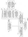
- FIG. 1is schematic cross-sectional view of a CNT transistor
- FIG. 2is a schematic plan view of the CNT transistor of FIG. 1 ;
- FIG. 3is a schematic cross-sectional view of a complementary CNT device
- FIG. 4is a schematic plan view of the complementary CNT device of FIG. 2 ;
- FIG. 5is a schematic flow diagram illustrating embodiments of the method of forming the structures of FIG. 1 and FIG. 2 .
- CNTcarbon nanotube
- CNTFETsCNT field effect transistors
- CMOScomplementary metal oxide semiconductor
- Vtthreshold voltage
- One methodcomprises doping the surface of the source/drain regions of the CNT with organic molecules so that either a p-type or an n-type FET is formed. This method requires additional processing steps during the formation of the FETS and does not allow a user to take advantage of this ambipolar property.
- Another methodcomprises introducing source/drain gates over the source/drain regions of the CNT between the source/drain electrodes and the front gate. A preselected voltage applied to the source/drain gates can be used to form electron layers or hole layers in the end regions of the CNT, so as to form an n-type FET or a p-type FET, respectively.
- the size of these source/drain gatesis limited due to the limited space between the electrodes and the front gate. Additionally, the position of the source/drain gates above the CNT causes parasitic resistance between the source/drain gates and the source/drain electrodes and also causes parasitic capacitance between the source/drain gates and the front gate. Therefore, it would be advantageous to provide an improved CNTFET, and more particularly, an improved complementary CNT device configured to overcome intrinsic ambipolar properties and to allow for threshold voltage adjustments.
- CNTcarbon nanotube
- FETsfield effect transistors
- One embodiment of the inventionprovides either a stable p-type CNTFET or a stable n-type CNTFET.
- Another embodiment of the inventionprovides a complementary CNT device (e.g., a complementary CNT inverter) that incorporates both a stable p-type CNTFET and a stable n-type CNTFET.
- the structures of the inventionuse “virtual” source/drain gates together with a back gate in order to describe a fully integrated CNT technology (including a CNTFET and a complementary CNT device).
- VSDvirtual source/drain
- a CNTis introduced above the two gate layers.
- source/drain contactsi.e., source/drain electrodes
- a front gatei.e., an active gate
- FIGS. 1 and 2in combination illustrate an embodiment of a stable n-type CNTFET or p-type CNTFET 100 in an insulating material 102 (e.g., single or multiple layers of an oxide or other dielectric material, including shallow trench isolation structures and/or other isolation structures) above a substrate 103 .
- the CNTFET 100comprises at least one carbon nanotube 110 (CNT) having a first side 117 , a second side 118 and opposing ends 111 .
- CNTcarbon nanotube 110
- FIG. 2that the CNTFET of the invention may incorporate either a single CNT or multiple CNTs 110 .
- the CNT 110has a central channel region 113 and source/drain electrodes 105 on either side of the channel region 113 (i.e., at the opposing ends 111 ).
- the source/drain electrodes 105contact the first side 117 of the CNT 110 at the opposing ends 111 .
- the CNTFET structure 100further comprises a first gate 115 (i.e., a front gate) for imparting a potential to the channel region 113 of the CNT 110 to turn the CNTFET 100 on or off, second gates 125 (i.e., source/drain gates) for imparting a preselected Fermi potential to the opposing ends 110 of the CNT 110 to configure the CNTFET 100 as either a p-FET or an n-FET, and optionally, a third gate 135 (i.e., a back gate) for imparting a preselected potential to the channel region 113 of the CNT 110 to adjust the threshold voltage of the CNTFET 100 .
- a first gate 115i.e., a front gate
- second gates 125i.e., source/drain gates
- a third gate 135i.e., a back gate
- Each gate(i.e., the first gate 115 , the second gates 125 and the third gate 135 ) comprises a gate conductor (e.g., a doped polysilicon, tungsten silicide, or any other suitable conductive material) on a gate dielectric (e.g., silicon dioxide or any other suitable dielectric material) adjacent to the CNT 110 .
- the gate conductors and gate dielectrics for the different gatesmay comprise the same or different conductive and dielectric materials.
- Each gatecan further comprise a gate contact (e.g., first gate contact 116 , second gate contacts 126 , and third gate contact 136 ) through which a voltage may be supplied to the corresponding gate.
- the first gate 115is positioned on the first side 117 of the CNT 110 above the channel region 113 and between the source/drain electrodes 105 .
- the second gates 125are positioned on the second side 118 of the CNT 110 opposite the source/drain electrodes 105 . Specifically, second gates 125 are positioned at each end 111 of the CNT 110 . As mentioned above, the second gates 125 are for setting (i.e., adjusting) the Fermi level of the end regions 111 of the CNT 110 to either the valence or the conduction band in order to configure the CNTFET 100 as either a p-FET or an n-FET, respectively.
- a negative biasi.e., a negative voltage
- second gates 125can promote a large population of holes within the CNT 110 by forcing the Fermi level to the valence band below the source/drain electrodes (i.e., by forcing a dominance of holes at the opposing ends of the CNT).
- the resulting structureacts as a p-FET.
- a positive biasi.e., a positive voltage
- applied to the second gates 125can promote a large population of electrons within the CNT by forcing the Fermi level to the conduction band below the source/drain electrodes (i.e., by forcing a dominance of electrons at the opposing ends of the CNT).
- the resulting structureacts as an n-FET.
- the second gates 125are formed such that there is a gap 128 (i.e., a dielectric filled space) between the two second gates 125 below the CNT 110 .
- the gap 128 between the two source/drain gates 125defines the area of the CNT 110 that is not acted upon by the second gates 125 and, thus, the size 108 of this gap 128 defines the channel region 113 of the CNTFET 110 .
- the first gate 115 and second gates 125can overlap to some degree (e.g., the first gate 115 can be aligned above the gap 128 and extend over a portion of the second gates 125 ) so as to optimize conduction in the carbon nanotube 110 .
- the relative positioning of the first gate 115 on the first side 117 of the CNT 110 and the second gates 125 on the second side 118 of the CNT 110minimizes parasitic capacitance between the second gates 125 and the first gate 115 and also avoids parasitic resistance between the second gates 125 and the source/drain electrodes 105 .
- a third gate 135can be positioned on the second side 118 of the CNT 110 below the channel region 113 .
- an additional preselected voltage applied to the third gate 135can be used to impart a preselected potential to the channel region 113 of the CNT 110 in order to independently adjust the threshold voltage of the CNTFET 100 .
- the third gate 135can be positioned closer to the CNT 110 than the second gates 125 to the extent that it does not obscure the effect of the second gates 125 on the CNT 110 .
- the third gate 135can also be positioned in the gap 128 between the two second gates 125 such that it is the same distance from the CNT 110 as the second gates 125 .
- drive current of the CNTFET 100can be optimized by positioning the third gate 135 below the gap 128 such the gate dielectric of the third gate (i.e., the back gate dielectric 107 ) is thicker than the gate dielectrics 114 and 106 of the first 115 and second 125 gates, respectively. If the third gate 135 is below the gap 128 , then the size 108 of the gap 128 further defines the area 109 of the carbon nanotube 110 upon which the third gate 135 can act (i.e., the area 109 to which a preselected potential can be imparted to adjust threshold voltage).
- FIGS. 3 and 4in combination illustrate an embodiment of a complementary CNT device 200 (e.g., a complementary inverter) that incorporates both a stable p-type CNTFET 400 and a stable n-type CNTFET 300 , as described above, in an insulating material 202 (e.g., an oxide) above a substrate 203 .
- the complementary CNT device 200comprises two adjacent transistors (i.e., a first transistor 300 and a second transistor 400 ).
- the first and second transistors 300 and 400each comprise at least one carbon nanotube 310 , 410 (as described above), source/drain electrodes 305 , 405 (as described above), a first gate 315 , 415 (as described above), second gates 325 , 425 (as described above) and optionally, a third gate 335 , 435 (as described above).
- the complementary CNT device 200 of the inventionare describe using a single CNT 310 , 410 in each of the first and second transistors 300 , 400 . However, it is anticipated and illustrated in FIG.
- the inventionmay incorporate either a single CNT 310 , 410 or multiple CNTs 310 , 410 in each of the first and second transistors 300 , 400 .
- Adjacent transistorsi.e., the first and second transistors 300 , 400
- a complementary CNT device 200e.g., a complementary CNT inverter
- the Fermi levels within the CNTs of adjacent transistorsso as to configure one of the transistors as an n-type CNTFET 300 and the other as a p-type CNTFET 400 .
- a positive voltage applied to the second gates 325forces the Fermi level of the opposing ends 311 of the first transistor 300 to the conduction band and, thereby, configures the first transistor 300 as a stable n-type transistor (see detailed discussion above).
- a negative voltage applied to the second gates 425forces the Fermi level of the opposing ends 411 of the second transistor 400 to the valence band and, thereby, configures the second transistor as a stable p-type transistor (see detailed discussion above).
- third gates 335 , 435are positioned below the channel region 313 , 413 of both of the first and second transistors 300 , 400 (e.g., as described above), the third gates 335 , 435 may be used to independently adjust the threshold voltages of the n-type and p-type CNTFETs 300 , 400 , respectively, within the complementary CNT device 200 .
- additional preselected voltages applied to the third gates 335 , 435can be used to impart preselected potentials to the channel regions of the CNTs so as to independently adjust the threshold voltages of the CNTFETs.
- FIG. 5illustrates a method of forming the p-type and n-type CNTFET structures 100 of FIGS. 1 and 2 and the complementary CNT device structure 200 of FIGS. 3 and 4 . More particularly, the following method steps provide for the formation of either a single CNTFET 100 (p-type or n-type) or a complementary CNT device 200 (with both a p-type 400 and an n-type 300 CNTFET).
- the methodcomprises forming at least one transistor such that each transistor (e.g., a single transistor or multiple adjacent transistors) is formed with a front gate, source/drain gates, and optionally, a back gate ( 500 ).
- the front gateis formed (at process 508 ) so that a potential can be imparted to the channel region of the CNT in order to turn the CNTFET on or off.
- the source/drain gatesare formed (at process 504 discussed below) so that a preselected bias (e.g., a preselected positive or negative voltage) applied to the source/drain gates can force the Fermi level of the opposing ends of the CNT to the valence or the conduction band, in order to configure the CNTFET as either a p-FET or an n-FET, respectively (at process 512 or 514 ).
- the back gateis optionally formed (at process 502 ) so that an additional preselected voltage applied to the back gate can impart a preselected potential on the channel region in order to independently adjust the threshold voltage of the CNTFET (at process 516 , see detailed discussion below).
- Each of the gate structuresare formed using conventional methods such that they each comprise a corresponding gate conductor (e.g., a doped polysilicon, tungsten silicide, or any other suitable conductive material) on a corresponding gate dielectric (e.g., silicon dioxide or any other suitable dielectric material) adjacent to the CNT.
- a corresponding gate conductore.g., a doped polysilicon, tungsten silicide, or any other suitable conductive material
- a corresponding gate dielectrice.g., silicon dioxide or any other suitable dielectric material
- At least one transistoris formed by optionally forming a back gate structure (e.g., on an insulator layer above a substrate) ( 502 ).
- Source/drain gatesare preferably formed above the back gate and separated by a gap such that the back gate is aligned below the gap ( 504 ).
- a carbon nanotube, having opposing ends and a channel region,is formed such that the source/drain gates are aligned below the opposing ends and such that the gap (and thus, the back gate) is below the channel region ( 506 ).
- the back gate dielectric between the back gate and the carbon nanotubecan be formed thicker than the source/drain gate dielectric between the second gates and the carbon nanotube in order to optimize drive current.
- Source/drain electrodesare formed above the carbon nanotube such that they contact the opposing ends opposite the source/drain gates ( 510 ).
- a front gateis also formed above the CNT ( 508 ). Specifically, the front gate is formed above the channel region between the source/drain electrodes.
- the at least one transistorcan be configured into either a p-FET or an n-FET by applying a negative voltage or positive voltage, respectively, to the source/drain electrodes ( 512 ). If at least two adjacent transistors are formed, those transistors can be incorporated into a complementary CNT inverter by configuring one of the two adjacent transistors as a stable p-type transistor and another of said two adjacent transistors as a stable n-type transistor ( 514 ). Once a single CNTFET is formed (at process 512 ) or a complementary CNT device with multiple CNTFETs is formed (at process 514 ), an additional preselected voltage can be applied to the back gate(s) to independently adjust the threshold voltage of each CNTFET ( 516 ).
- the back gate voltagemay be adjusted so that the potential of the channel region results in very few free electrons or holes when the front gate voltage is the same as the source voltage, but results in a large number of electrons when the front gate voltage, with respect to its source voltage, is above (a positive-valued) threshold voltage for n-type CNTFETs, or a large number of holes when the front gate voltage, with respect to its source voltage, is below (a negative-valued) threshold voltage for p-type CNTFETs.
- the absolute values of the threshold voltages of the p-type and n-type CNTFETsare each less than the power-supply voltage used to operate the complementary CNTFET circuitry, with the p-type threshold voltage less than zero and the n-type threshold voltage greater than zero.
- One embodiment of the inventionprovides either a stable p-type CNTFET or a stable n-type CNTFET.
- Another embodiment of the inventionprovides a complementary CNT device.
- source/drain gatesare introduced below the CNT opposite the source/drain electrodes. The source/drain gates are used to position the Fermi level of the ends of the CNT to the conduction or valence bands so as to configure the FET as either an n-type or p-type CNTFET, respectively.
- Two adjacent FETsconfigured such that one is an n-type CNTFET and the other is a p-type CNTFET, can be incorporated into a complementary CNT device.
- a back gatecan also be introduced below the CNT and, particularly, below the channel region of the CNT opposite the front gate.
- These CNTFETSexhibit minimized parasitic capacitances and resistances and, thus, can be incorporated into very high density complementary circuits which use very little power and provide very high speed.
- improved circuit yieldfollows from the ability to adjust the threshold voltages of the CNTFETs in response to process, environment, or other variables.
- the fabrication costs associated with the CNTFETS of the inventionare lower than those associated with prior art technology due to the elimination of the steps that would otherwise be associated with doping of source and drain regions and from the increased circuit densities achievable
Landscapes
- Engineering & Computer Science (AREA)
- Chemical & Material Sciences (AREA)
- Nanotechnology (AREA)
- Physics & Mathematics (AREA)
- Mathematical Physics (AREA)
- Theoretical Computer Science (AREA)
- Crystallography & Structural Chemistry (AREA)
- Thin Film Transistor (AREA)
- Metal-Oxide And Bipolar Metal-Oxide Semiconductor Integrated Circuits (AREA)
Abstract
Description
- 1. Field of the Invention
- The invention generally relates to carbon nanotube semiconductor devices, and, more particularly, to a carbon nanotube field effect transistor that is configured to overcome intrinsic ambipolar properties and to allow for threshold voltage adjustments and to complementary carbon nanotube devices that incorporate such transistors.
- 2. Description of the Related Art
- A carbon nanotube (i.e., nanoscale hollow graphite tube) can, depending on its conformational geometry, exhibit either metallic or semiconductor properties. In recent years the use of semiconductor carbon nanotube (CNT) devices, such as CNT field effect transistors (CNTFETs), has been proposed to overcome scaling limits encountered by silicon semiconductor devices. Additionally, since semiconductor CNTs exhibit high transconductance, a desirable property for complementary devices, such as complementary inverters, complementary CNTFET circuitry which mimics complementary metal oxide semiconductor (CMOS) technology has been proposed. However, there are two basic barriers to doing so. First, CNTs form intrinsically ambipolar FETs due to the formation of Schottky-Barrier contacts at the junction of the source and drain electrodes and the CNT. Second, since the threshold voltage (Vt) of CNTFETs are not easily controlled via conventional means, such as doping of the channel, some means is required to adjust the threshold voltages to complementary CNTFETs-compatible values. Therefore, it would be advantageous to provide a CNTFET, and more particularly, a complementary CNT device incorporating carbon nanotube transistors that are configured to overcome intrinsic ambipolar properties and to allow for threshold voltage adjustments.
- In view of the foregoing, disclosed herein is a carbon nanotube (CNT) technology that overcomes the intrinsic ambipolar properties of CNT field effect transistors (FETs) and optionally, allows for independent threshold adjustments. One embodiment of the invention provides either a stable p-type CNTFET or a stable n-type CNTFET. Another embodiment of the invention provides a complementary CNT device (e.g., a complementary CNT inverter) that incorporates both a stable p-type CNTFET and a stable n-type CNTFET, as described.
- More particularly, an embodiment of the stable n-type CNTFET or p-type CNTFET of the invention comprises at least one carbon nanotube (CNT) having a first side, a second side and opposing ends. For illustration purposes, embodiments of the CNTFET of the invention are described herein using a single CNT. However, it is anticipated and illustrated in the accompanying figures, that the CNTFET of the invention may incorporate either a single CNT or multiple CNTs. Specifically, the CNT has a central channel region and source/drain electrodes on either side of the channel region (i.e., at the opposing ends). The source/drain electrodes contact the first side of the CNT at the opposing ends. The CNTFET structure further comprises a first gate (i.e., a front gate) for imparting a potential to the channel region of the CNT to render the CNTFET in a conducting or non-conducting state (i.e., turn on or off the FET), second gates (i.e., source/drain gates) for forcing the Fermi level of the opposing ends of the CNT to either the valence or the conduction bands so as to configure the CNTFET as either a p-FET or an n-FET, and optionally, a third gate (i.e., a back gate) for imparting a preselected potential to the channel region of the CNT to adjust the threshold voltage of the CNTFET. Each gate (i.e., the first gate, second gates and third gate) comprises a gate conductor (e.g., a doped polysilicon, tungsten silicide, or any other suitable conductive material) and a gate dielectric (e.g., silicon dioxide or any other suitable dielectric material).
- The first gate is positioned on the first side of the CNT above the channel region and between the source/drain electrodes.
- The second gates are positioned on the second side of the CNT opposite the source/drain electrodes. Specifically, second gates are positioned at each end of the CNT. As mentioned above, the second gates are adjusted to a preselected (either negative or positive) voltage in order to configure the CNTFET as either a p-FET or an n-FET, respectively. For example, a negative bias (i.e., a negative voltage) applied to the source/drain electrodes of the CNT(s) can promote the population of holes within the CNT, by pushing the Fermi level to the valence band and resulting in dominance of holes below the source/drain electrodes. The resulting structure acts as a p-FET. Alternatively, a positive bias (i.e., a positive voltage) applied to the source/drain electrodes of the CNT can promote the population of electrons within the CNT, by forcing the Fermi level to the conduction band and resulting in a dominance of electrons below the source/drain electrodes. The resulting structure acts as an n-FET. The second gates are formed such that there is a gap (i.e., a dielectric filled space) between the two second gates below the CNT. The gap between the two source/drain gates defines the area of the CNT that is not acted upon by the second gates and, thus, the size of this gap defines the channel region of the CNTFET. Additionally, the first and second gates can overlap to some degree (e.g., the first gate can be aligned above the gap and extend over a portion of the second gates) so as to optimize conduction in the carbon nanotube. Furthermore, the relative positioning of the first gate on the first side of the CNT and the second gates on the second side of the CNT minimizes parasitic capacitance between the second gates and the first gate and avoids parasitic resistance between the second gates and the source/drain electrodes.
- Optionally, a third gate can be positioned on the second side of the CNT below the channel region. As mentioned above, the third gate can be biased to an additional preselected voltage to adjust the threshold voltage of the CNTFET. The third gate can be positioned closer to the CNT than the second gates to the extent that it does not obscure the effect of the second gates on the CNT in the vicinity of the source/drain electrodes. The third gate can also be positioned in the gap between the two second gates such that it is the same distance from the CNT as the second gates. However, the drive current of the CNTFET can be optimized by positioning the third gate below the gap such the gate dielectric of the third gate is thicker than that of both the first gate and the second gates. If the third gate is below the gap, then the size of the gap further defines the area of the carbon nanotube upon which the third gate can act (i.e., the area to which preselected potential can be imparted to adjust threshold voltage).
- As mentioned above, another embodiment of the invention provides a complementary CNT device (e.g., a complementary inverter) that incorporates both a stable p-type CNTFET and a stable n-type CNTFET, as described above. More particularly, an embodiment of the complementary CNT device comprises two transistors (i.e., a first transistor and a second transistor). The first and second transistors each comprise at least one carbon nanotube (as described above), source/drain electrodes (as described above), a first gate (as describe above), second gates (as described above) and optionally, a third gate (as described above). As with the CNTFET of the invention, for illustration purposes, embodiments of the complementary CNT device of the invention are described using a single CNT in each of the first and second transistors. However, it is anticipated and illustrated in the accompanying figures, that the invention may incorporate either a single CNT or multiple CNTs in each of the first and second transistors. Adjacent transistors (i.e., the first and second transistors) can be incorporated into a complementary CNT device (e.g., a complementary CNT inverter) by configuring one of the transistors as an n-type CNTFET and the other as a p-type CNTFET. Specifically, a positive voltage applied to the opposing ends of the first transistor via the second gates configures the first transistor as a stable n-type transistor (see detailed discussion above). A negative voltage applied to the opposing ends of the second transistor via the second gates configures the second transistor as a stable p-type transistor (see detailed discussion above). Additionally, if third gates are positioned below the channel region of both of the first and second transistors (e.g., as described above), the third gates may be used to independently adjust the threshold voltages of the n-type and p-type CNTFETs, respectively, within the complementary CNT device.
- Also, disclosed herein is a method of forming the CNTFET structures and complementary CNT device structure of the invention. More particularly, the following method steps provide for the formation of either a single CNTFET (p-type or n-type) or a complementary CNT device (with both a p-type and an n-type CNTFET).
- The method comprises forming at least one transistor such that each transistor (e.g., a single transistor or multiple adjacent transistors) is formed with a front gate, source/drain gates, and optionally, a back gate. A preselected voltage can be applied to the front gate so as to impart a potential to the channel region of the CNT and, thereby, turn the CNTFET on or off. Another preselected voltage (e.g., a preselected negative or positive voltage) can be applied to the source/drain gates in order to force the Fermi level in the opposing ends of the CNT to the valence or conduction bands and, thereby, configure the CNTFET as either a p-FET or an n-FET, respectively. Optionally, an additional preselected voltage can be applied to the back gate so as to impart an additional preselected potential to the channel region to independently adjust the threshold voltage of the CNTFET. Each of the gate structures (i.e., the front gate, the source/drain gates and the back gate) are formed using conventional methods such that they each comprise a corresponding gate conductor (e.g., a doped polysilicon, tungsten silicide, or any other suitable conductive material) and a corresponding gate dielectric (e.g., silicon dioxide or any other suitable dielectric material) adjacent the CNT.
- More particularly, at least one transistor is formed by optionally forming a back gate structure (e.g., on an insulator layer above a substrate). Source/drain gates are preferably formed above the back gate and separated by a gap such that the back gate is aligned below the gap. A carbon nanotube, having opposing ends and a channel region, is formed such that the source/drain gates are aligned below the opposing ends and such that the gap (and thus, the back gate) is below the channel region. Those skilled in the art will recognize that by forming the source/drain gates above the back gate, the back gate dielectric between the back gate and the carbon nanotube can be formed thicker than the source/drain gate dielectric between the second gates and the carbon nanotube in order to optimize drive current. Additionally, source/drain electrodes are formed above the carbon nanotube such that they contact the opposing ends of the carbon nanotube, opposite the source/drain gates. A front gate is also formed above the CNT. Specifically, a front gate is formed above the channel region between the source/drain electrodes. By aligning the front gate above the gap and extending the front gate over a portion of each of the source/drain gates conduction in the carbon nanotube can be optimized. The at least one transistor can be configured into either a p-FET or an n-FET by imparting a negative voltage or positive potential, respectively, to the opposing ends of the CNT opposite the source/drain electrodes. If at least two adjacent transistors are formed, those transistors can be incorporated into a complementary CNT inverter by configuring one of the two adjacent transistors as a stable p-type transistor and another of said two a stable n-type transistor.
- These and other aspects of embodiments of the invention will be better appreciated and understood when considered in conjunction with the following description and the accompanying drawings. It should be understood, however, that the following description, while indicating preferred embodiments of the invention and numerous specific details thereof, is given by way of illustration and not of limitation. Many changes and modifications may be made within the scope of the embodiments of the invention without departing from the spirit thereof, and the invention includes all such modifications.
- The embodiments of the invention will be better understood from the following detailed description with reference to the drawings, in which:
FIG. 1 is schematic cross-sectional view of a CNT transistor;FIG. 2 is a schematic plan view of the CNT transistor ofFIG. 1 ;FIG. 3 is a schematic cross-sectional view of a complementary CNT device;FIG. 4 is a schematic plan view of the complementary CNT device ofFIG. 2 ; andFIG. 5 is a schematic flow diagram illustrating embodiments of the method of forming the structures ofFIG. 1 andFIG. 2 .- The embodiments of the invention and the various features and advantageous details thereof are explained more fully with reference to the non-limiting embodiments that are illustrated in the accompanying drawings and detailed in the following description. It should be noted that the features illustrated in the drawings are not necessarily drawn to scale. Descriptions of well-known components and processing techniques are omitted so as to not unnecessarily obscure the embodiments of the invention. The examples used herein are intended merely to facilitate an understanding of ways in which the embodiments of the invention may be practiced and to further enable those of skill in the art to practice the embodiments of the invention. Accordingly, the examples should not be construed as limiting the scope of the invention.
- As mentioned above, the use of carbon nanotube (CNT) devices, such as CNT field effect transistors (CNTFETs), has been proposed to overcome scaling limits encountered by silicon semiconductor devices. Additionally, CNTs exhibit high transconductance, a desirable property for complementary devices (e.g., complementary inverters). Thus, it would be desirable to use CNTs to form complementary CNTFET circuitry which mimics complementary metal oxide semiconductor (CMOS) technology. However, there are two basic barriers to doing so. First, CNTs form intrinsically ambipolar FETs due to the formation of Schottky-Barrier contacts at the junction between the source and drain electrodes and the CNT. Second, since the threshold voltage (Vt) of CNTFETs are intrinsically negative for n-type FETs and positive for p-type FETs, some means is required to adjust the threshold voltages to complementary CNTFETs-compatible values.
- A few prior-art methods have been proposed to overcoming this ambipolar property in CNTFETS. One method comprises doping the surface of the source/drain regions of the CNT with organic molecules so that either a p-type or an n-type FET is formed. This method requires additional processing steps during the formation of the FETS and does not allow a user to take advantage of this ambipolar property. Another method comprises introducing source/drain gates over the source/drain regions of the CNT between the source/drain electrodes and the front gate. A preselected voltage applied to the source/drain gates can be used to form electron layers or hole layers in the end regions of the CNT, so as to form an n-type FET or a p-type FET, respectively. However, the size of these source/drain gates is limited due to the limited space between the electrodes and the front gate. Additionally, the position of the source/drain gates above the CNT causes parasitic resistance between the source/drain gates and the source/drain electrodes and also causes parasitic capacitance between the source/drain gates and the front gate. Therefore, it would be advantageous to provide an improved CNTFET, and more particularly, an improved complementary CNT device configured to overcome intrinsic ambipolar properties and to allow for threshold voltage adjustments.
- In view of the foregoing, disclosed herein is a carbon nanotube (CNT) technology that overcomes the intrinsic ambipolar properties of CNT field effect transistors (FETs) and optionally, allows for independent threshold adjustments. One embodiment of the invention provides either a stable p-type CNTFET or a stable n-type CNTFET. Another embodiment of the invention provides a complementary CNT device (e.g., a complementary CNT inverter) that incorporates both a stable p-type CNTFET and a stable n-type CNTFET. In order to overcome the ambipolar properties of CNTFETs and to independently adjust threshold voltage of CNTFETs, the structures of the invention use “virtual” source/drain gates together with a back gate in order to describe a fully integrated CNT technology (including a CNTFET and a complementary CNT device). Specifically, two gate layers are introduced above a substrate to form self-aligned virtual source/drain (VSD) gates and a back-gate, respectively, for each CNTFET. A CNT is introduced above the two gate layers. Above the CNT, source/drain contacts (i.e., source/drain electrodes) are formed such that they contact the ends of the CNT. Finally, a front gate (i.e., an active gate) is formed between the two electrodes above a channel region in the CNT. In this manner parasitic capacitances and resistances are minimized.
- More particularly,
FIGS. 1 and 2 in combination illustrate an embodiment of a stable n-type CNTFET or p-type CNTFET 100 in an insulating material102 (e.g., single or multiple layers of an oxide or other dielectric material, including shallow trench isolation structures and/or other isolation structures) above asubstrate 103. TheCNTFET 100 comprises at least one carbon nanotube110 (CNT) having afirst side 117, asecond side 118 and opposing ends111. For illustration purposes, embodiments of the CNTFET are described herein using a single CNT. However, it is anticipated and illustratedFIG. 2 , that the CNTFET of the invention may incorporate either a single CNT ormultiple CNTs 110. Specifically, theCNT 110 has acentral channel region 113 and source/drain electrodes 105 on either side of the channel region113 (i.e., at the opposing ends111). The source/drain electrodes 105 contact thefirst side 117 of theCNT 110 at the opposing ends111. TheCNTFET structure 100 further comprises a first gate115 (i.e., a front gate) for imparting a potential to thechannel region 113 of theCNT 110 to turn theCNTFET 100 on or off, second gates125 (i.e., source/drain gates) for imparting a preselected Fermi potential to the opposing ends110 of theCNT 110 to configure theCNTFET 100 as either a p-FET or an n-FET, and optionally, a third gate135 (i.e., a back gate) for imparting a preselected potential to thechannel region 113 of theCNT 110 to adjust the threshold voltage of theCNTFET 100. Each gate (i.e., thefirst gate 115, thesecond gates 125 and the third gate135) comprises a gate conductor (e.g., a doped polysilicon, tungsten silicide, or any other suitable conductive material) on a gate dielectric (e.g., silicon dioxide or any other suitable dielectric material) adjacent to theCNT 110. The gate conductors and gate dielectrics for the different gates may comprise the same or different conductive and dielectric materials. Each gate can further comprise a gate contact (e.g.,first gate contact 116,second gate contacts 126, and third gate contact136) through which a voltage may be supplied to the corresponding gate. - The
first gate 115 is positioned on thefirst side 117 of theCNT 110 above thechannel region 113 and between the source/drain electrodes 105. - The
second gates 125 are positioned on thesecond side 118 of theCNT 110 opposite the source/drain electrodes 105. Specifically,second gates 125 are positioned at eachend 111 of theCNT 110. As mentioned above, thesecond gates 125 are for setting (i.e., adjusting) the Fermi level of theend regions 111 of theCNT 110 to either the valence or the conduction band in order to configure theCNTFET 100 as either a p-FET or an n-FET, respectively. For example, a negative bias (i.e., a negative voltage) applied tosecond gates 125 can promote a large population of holes within theCNT 110 by forcing the Fermi level to the valence band below the source/drain electrodes (i.e., by forcing a dominance of holes at the opposing ends of the CNT). The resulting structure acts as a p-FET. Alternatively, as illustrated inFIG. 1 , a positive bias (i.e., a positive voltage) applied to thesecond gates 125 can promote a large population of electrons within the CNT by forcing the Fermi level to the conduction band below the source/drain electrodes (i.e., by forcing a dominance of electrons at the opposing ends of the CNT). The resulting structure acts as an n-FET. Thesecond gates 125 are formed such that there is a gap128 (i.e., a dielectric filled space) between the twosecond gates 125 below theCNT 110. Thegap 128 between the two source/drain gates 125 defines the area of theCNT 110 that is not acted upon by thesecond gates 125 and, thus, thesize 108 of thisgap 128 defines thechannel region 113 of theCNTFET 110. Additionally, thefirst gate 115 andsecond gates 125 can overlap to some degree (e.g., thefirst gate 115 can be aligned above thegap 128 and extend over a portion of the second gates125) so as to optimize conduction in thecarbon nanotube 110. Furthermore, the relative positioning of thefirst gate 115 on thefirst side 117 of theCNT 110 and thesecond gates 125 on thesecond side 118 of theCNT 110 minimizes parasitic capacitance between thesecond gates 125 and thefirst gate 115 and also avoids parasitic resistance between thesecond gates 125 and the source/drain electrodes 105. - Optionally, a
third gate 135 can be positioned on thesecond side 118 of theCNT 110 below thechannel region 113. As mentioned above, an additional preselected voltage applied to thethird gate 135 can be used to impart a preselected potential to thechannel region 113 of theCNT 110 in order to independently adjust the threshold voltage of theCNTFET 100. Thethird gate 135 can be positioned closer to theCNT 110 than thesecond gates 125 to the extent that it does not obscure the effect of thesecond gates 125 on theCNT 110. Thethird gate 135 can also be positioned in thegap 128 between the twosecond gates 125 such that it is the same distance from theCNT 110 as thesecond gates 125. However, drive current of theCNTFET 100 can be optimized by positioning thethird gate 135 below thegap 128 such the gate dielectric of the third gate (i.e., the back gate dielectric107) is thicker than thegate dielectrics third gate 135 is below thegap 128, then thesize 108 of thegap 128 further defines thearea 109 of thecarbon nanotube 110 upon which thethird gate 135 can act (i.e., thearea 109 to which a preselected potential can be imparted to adjust threshold voltage). FIGS. 3 and 4 in combination illustrate an embodiment of a complementary CNT device200 (e.g., a complementary inverter) that incorporates both a stable p-type CNTFET 400 and a stable n-type CNTFET 300, as described above, in an insulating material202 (e.g., an oxide) above asubstrate 203. More particularly, thecomplementary CNT device 200 comprises two adjacent transistors (i.e., afirst transistor 300 and a second transistor400). The first andsecond transistors carbon nanotube 310,410 (as described above), source/drain electrodes 305,405 (as described above), afirst gate 315,415 (as described above),second gates 325,425 (as described above) and optionally, athird gate 335,435 (as described above). As with theCNTFET 100 of the invention, for illustration purposes, embodiments of thecomplementary CNT device 200 of the invention are describe using asingle CNT second transistors FIG. 4 , that the invention may incorporate either asingle CNT multiple CNTs second transistors second transistors 300,400) can be incorporated into a complementary CNT device200 (e.g., a complementary CNT inverter) by adjusting the Fermi levels within the CNTs of adjacent transistors so as to configure one of the transistors as an n-type CNTFET 300 and the other as a p-type CNTFET 400. Specifically, a positive voltage applied to thesecond gates 325 forces the Fermi level of the opposing ends311 of thefirst transistor 300 to the conduction band and, thereby, configures thefirst transistor 300 as a stable n-type transistor (see detailed discussion above). A negative voltage applied to thesecond gates 425 forces the Fermi level of the opposing ends411 of thesecond transistor 400 to the valence band and, thereby, configures the second transistor as a stable p-type transistor (see detailed discussion above). Additionally, ifthird gates channel region second transistors 300,400 (e.g., as described above), thethird gates type CNTFETs complementary CNT device 200. Specifically, additional preselected voltages applied to thethird gates FIG. 5 illustrates a method of forming the p-type and n-type CNTFET structures 100 ofFIGS. 1 and 2 and the complementaryCNT device structure 200 ofFIGS. 3 and 4 . More particularly, the following method steps provide for the formation of either a single CNTFET100 (p-type or n-type) or a complementary CNT device200 (with both a p-type 400 and an n-type 300 CNTFET).- The method comprises forming at least one transistor such that each transistor (e.g., a single transistor or multiple adjacent transistors) is formed with a front gate, source/drain gates, and optionally, a back gate (500). The front gate is formed (at process508) so that a potential can be imparted to the channel region of the CNT in order to turn the CNTFET on or off. The source/drain gates are formed (at
process 504 discussed below) so that a preselected bias (e.g., a preselected positive or negative voltage) applied to the source/drain gates can force the Fermi level of the opposing ends of the CNT to the valence or the conduction band, in order to configure the CNTFET as either a p-FET or an n-FET, respectively (atprocess 512 or514). The back gate is optionally formed (at process502) so that an additional preselected voltage applied to the back gate can impart a preselected potential on the channel region in order to independently adjust the threshold voltage of the CNTFET (atprocess 516, see detailed discussion below). Each of the gate structures (i.e., the front gate, the source/drain gates and the back gate) are formed using conventional methods such that they each comprise a corresponding gate conductor (e.g., a doped polysilicon, tungsten silicide, or any other suitable conductive material) on a corresponding gate dielectric (e.g., silicon dioxide or any other suitable dielectric material) adjacent to the CNT. - More particularly, at least one transistor is formed by optionally forming a back gate structure (e.g., on an insulator layer above a substrate) (502). Source/drain gates are preferably formed above the back gate and separated by a gap such that the back gate is aligned below the gap (504). A carbon nanotube, having opposing ends and a channel region, is formed such that the source/drain gates are aligned below the opposing ends and such that the gap (and thus, the back gate) is below the channel region (506). Those skilled in the art will recognize that by forming the source/drain gates above the back gate, the back gate dielectric between the back gate and the carbon nanotube can be formed thicker than the source/drain gate dielectric between the second gates and the carbon nanotube in order to optimize drive current. Source/drain electrodes are formed above the carbon nanotube such that they contact the opposing ends opposite the source/drain gates (510). A front gate is also formed above the CNT (508). Specifically, the front gate is formed above the channel region between the source/drain electrodes. By aligning the front gate above the gap and extending the front gate over a portion of each of the source/drain gates conduction in the carbon nanotube can be optimized (509). The at least one transistor can be configured into either a p-FET or an n-FET by applying a negative voltage or positive voltage, respectively, to the source/drain electrodes (512). If at least two adjacent transistors are formed, those transistors can be incorporated into a complementary CNT inverter by configuring one of the two adjacent transistors as a stable p-type transistor and another of said two adjacent transistors as a stable n-type transistor (514). Once a single CNTFET is formed (at process512) or a complementary CNT device with multiple CNTFETs is formed (at process514), an additional preselected voltage can be applied to the back gate(s) to independently adjust the threshold voltage of each CNTFET (516). In particular, the back gate voltage may be adjusted so that the potential of the channel region results in very few free electrons or holes when the front gate voltage is the same as the source voltage, but results in a large number of electrons when the front gate voltage, with respect to its source voltage, is above (a positive-valued) threshold voltage for n-type CNTFETs, or a large number of holes when the front gate voltage, with respect to its source voltage, is below (a negative-valued) threshold voltage for p-type CNTFETs. For complementary CNTFET operation the absolute values of the threshold voltages of the p-type and n-type CNTFETs are each less than the power-supply voltage used to operate the complementary CNTFET circuitry, with the p-type threshold voltage less than zero and the n-type threshold voltage greater than zero.
- Therefore, disclosed above is a CNT technology that overcomes the intrinsic ambipolar properties of CNTFETs and optionally, allows for independent threshold adjustments. One embodiment of the invention provides either a stable p-type CNTFET or a stable n-type CNTFET. Another embodiment of the invention provides a complementary CNT device. In order to overcome the ambipolar properties of in a CNTFET, source/drain gates are introduced below the CNT opposite the source/drain electrodes. The source/drain gates are used to position the Fermi level of the ends of the CNT to the conduction or valence bands so as to configure the FET as either an n-type or p-type CNTFET, respectively. Two adjacent FETs, configured such that one is an n-type CNTFET and the other is a p-type CNTFET, can be incorporated into a complementary CNT device. In order to independently adjust the threshold voltage of an individual CNTFET, a back gate can also be introduced below the CNT and, particularly, below the channel region of the CNT opposite the front gate. These CNTFETS exhibit minimized parasitic capacitances and resistances and, thus, can be incorporated into very high density complementary circuits which use very little power and provide very high speed. Additionally, improved circuit yield follows from the ability to adjust the threshold voltages of the CNTFETs in response to process, environment, or other variables. Lastly, the fabrication costs associated with the CNTFETS of the invention are lower than those associated with prior art technology due to the elimination of the steps that would otherwise be associated with doping of source and drain regions and from the increased circuit densities achievable
- The foregoing description of the specific embodiments will so fully reveal the general nature of the invention that others can, by applying current knowledge, readily modify and/or adapt for various applications such specific embodiments without departing from the generic concept, and, therefore, such adaptations and modifications should and are intended to be comprehended within the meaning and range of equivalents of the disclosed embodiments. It is to be understood that the phraseology or terminology employed herein is for the purpose of description and not of limitation. Therefore, while the invention has been described in terms of preferred embodiments, those skilled in the art will recognize that the invention can be practiced with modification within the spirit and scope of the appended claims.
Claims (22)
Priority Applications (3)
| Application Number | Priority Date | Filing Date | Title |
|---|---|---|---|
| US11/164,109US7492015B2 (en) | 2005-11-10 | 2005-11-10 | Complementary carbon nanotube triple gate technology |
| CNB2006101444838ACN100561750C (en) | 2005-11-10 | 2006-11-08 | Carbon nanotube transistor and method of forming carbon nanotube device |
| JP2006304611AJP5220300B2 (en) | 2005-11-10 | 2006-11-09 | Carbon nanotube field effect transistor, method of forming the same, and complementary carbon nanotube device |
Applications Claiming Priority (1)
| Application Number | Priority Date | Filing Date | Title |
|---|---|---|---|
| US11/164,109US7492015B2 (en) | 2005-11-10 | 2005-11-10 | Complementary carbon nanotube triple gate technology |
Publications (2)
| Publication Number | Publication Date |
|---|---|
| US20070102747A1true US20070102747A1 (en) | 2007-05-10 |
| US7492015B2 US7492015B2 (en) | 2009-02-17 |
Family
ID=38002877
Family Applications (1)
| Application Number | Title | Priority Date | Filing Date |
|---|---|---|---|
| US11/164,109Expired - Fee RelatedUS7492015B2 (en) | 2005-11-10 | 2005-11-10 | Complementary carbon nanotube triple gate technology |
Country Status (3)
| Country | Link |
|---|---|
| US (1) | US7492015B2 (en) |
| JP (1) | JP5220300B2 (en) |
| CN (1) | CN100561750C (en) |
Cited By (21)
| Publication number | Priority date | Publication date | Assignee | Title |
|---|---|---|---|---|
| US20080237738A1 (en)* | 2007-03-27 | 2008-10-02 | Christoph Andreas Kleint | Integrated circuit, cell, cell arrangement, method for manufacturing an integrated circuit, method for manufacturing a cell arrangement; memory module |
| US20080290418A1 (en)* | 2007-05-25 | 2008-11-27 | Kalburge Amol M | Method for Integrating Nanotube Devices with CMOS for RF/Analog SoC Applications |
| US20080296689A1 (en)* | 2007-05-29 | 2008-12-04 | Dawei Wang | Nanotube dual gate transistor and method of operating the same |
| US20090242260A1 (en)* | 2008-04-01 | 2009-10-01 | Altebaeumer Thomas Heinz-Helmut | Device interconnects |
| US20090242912A1 (en)* | 2008-04-01 | 2009-10-01 | Altebaeumer Thomas Heinz-Helmut | Multifunctional tape |
| US20090256594A1 (en)* | 2008-04-09 | 2009-10-15 | International Business Machines Corporation | Nanoelectromechanical digital inverter |
| US20090267647A1 (en)* | 2008-04-25 | 2009-10-29 | Samsung Electronics Co., Ltd. | Convertible logic circuits comprising carbon nanotube transistors having ambipolar charateristics |
| US20100065899A1 (en)* | 2008-09-16 | 2010-03-18 | Kim Suk-Pil | Semiconductor devices including auxiliary gate electrodes and methods of fabricating the same |
| US20100207102A1 (en)* | 2009-02-18 | 2010-08-19 | Samsung Electronics Co., Ltd. | Static random access memories having carbon nanotube thin films |
| US20100295022A1 (en)* | 2009-05-21 | 2010-11-25 | International Business Machines Corporation | Nanowire Mesh FET with Multiple Threshold Voltages |
| KR101076767B1 (en)* | 2009-02-11 | 2011-10-26 | 광주과학기술원 | Nano-logic circuits and the method of manufacturing the same |
| WO2011088340A3 (en)* | 2010-01-15 | 2011-12-08 | Board Of Regents, The University Of Texas System | A carbon nanotube crossbar based nano-architecture |
| US20110315961A1 (en)* | 2010-06-29 | 2011-12-29 | International Business Machines Corporation | Ultrathin Spacer Formation for Carbon-Based FET |
| EP2320456A4 (en)* | 2008-07-25 | 2014-08-06 | Univ Tohoku | DEVICE WITH COMPLEMENTARY LOGIC DOOR |
| WO2014165950A1 (en)* | 2013-04-10 | 2014-10-16 | Firmano Lino Junior | Non-deposit forming catalytic additive for additive oil cracking, and for fuel octane increase and combustion |
| US20150364472A1 (en)* | 2014-06-12 | 2015-12-17 | Samsung Electronics Co., Ltd. | Semiconductor device, method of manufacturing the same, and electronic device including the same |
| US20170040443A1 (en)* | 2014-04-24 | 2017-02-09 | University Of Florida Research Foundation, Inc. | Tunable barrier transistors for high power electronics |
| US10594319B2 (en)* | 2016-06-03 | 2020-03-17 | Northwestern University | System and method for complimentary VT-drop ambipolar carbon nanotube logic |
| US20220052283A1 (en)* | 2019-09-05 | 2022-02-17 | Taiwan Semiconductor Manufacturing Company, Ltd. | Method of manufacturing a field effect transistor using carbon nanotubes and a field effect transistor |
| US11844227B2 (en) | 2019-06-05 | 2023-12-12 | Boe Technology Group Co., Ltd. | Thin film transistor and manufacturing method thereof, and electronic device |
| US12114515B2 (en) | 2018-12-21 | 2024-10-08 | National Research Council Of Canada | Thin film transistors comprising carbon nanotube networks encapsulated by a polymeric layer and methods for the manufacture thereof |
Families Citing this family (31)
| Publication number | Priority date | Publication date | Assignee | Title |
|---|---|---|---|---|
| WO2007099642A1 (en)* | 2006-03-03 | 2007-09-07 | Fujitsu Limited | Field effect transistor employing carbon nanotube, method for fabricating the same and sensor |
| US8004043B2 (en) | 2006-12-19 | 2011-08-23 | Intel Corporation | Logic circuits using carbon nanotube transistors |
| JP2009252798A (en)* | 2008-04-01 | 2009-10-29 | Mitsumi Electric Co Ltd | Carbon nanotube field-effect transistor and its fabrication process |
| KR101026160B1 (en) | 2008-11-26 | 2011-04-05 | 한국원자력연구원 | Hybrid nanodevice logic circuit and manufacturing method thereof |
| JP5544796B2 (en)* | 2009-09-10 | 2014-07-09 | ソニー株式会社 | Three-terminal electronic device and two-terminal electronic device |
| US8404539B2 (en) | 2010-07-08 | 2013-03-26 | International Business Machines Corporation | Self-aligned contacts in carbon devices |
| US8344358B2 (en) | 2010-09-07 | 2013-01-01 | International Business Machines Corporation | Graphene transistor with a self-aligned gate |
| US9076873B2 (en) | 2011-01-07 | 2015-07-07 | International Business Machines Corporation | Graphene devices with local dual gates |
| US8455365B2 (en) | 2011-05-19 | 2013-06-04 | Dechao Guo | Self-aligned carbon electronics with embedded gate electrode |
| US8557097B2 (en)* | 2011-09-09 | 2013-10-15 | International Business Machines Corporation | Embedding a nanotube inside a nanopore for DNA translocation |
| CN102487124B (en) | 2011-09-19 | 2014-07-23 | 中国科学院物理研究所 | Nanometer multilayer film, field-effect tube, sensor, random access memory and preparation method |
| US8895417B2 (en)* | 2011-11-29 | 2014-11-25 | International Business Machines Corporation | Reducing contact resistance for field-effect transistor devices |
| US8772910B2 (en) | 2011-11-29 | 2014-07-08 | International Business Machines Corporation | Doping carbon nanotubes and graphene for improving electronic mobility |
| JP2013179274A (en)* | 2012-02-09 | 2013-09-09 | Nippon Telegr & Teleph Corp <Ntt> | Field effect transistor and manufacturing method of the same |
| US9130568B2 (en) | 2012-08-09 | 2015-09-08 | Ecole Polytechnique Federale De Lausanne (Epfl) | Controllable polarity FET based arithmetic and differential logic |
| US9287406B2 (en)* | 2013-06-06 | 2016-03-15 | Macronix International Co., Ltd. | Dual-mode transistor devices and methods for operating same |
| CN104103692A (en)* | 2014-07-14 | 2014-10-15 | 南京邮电大学 | Carbon nanotube field effect transistor (CNTFET) with peak-symmetric linearity doped structure |
| CA2971589C (en) | 2014-12-18 | 2021-09-28 | Edico Genome Corporation | Chemically-sensitive field effect transistor |
| US9859394B2 (en) | 2014-12-18 | 2018-01-02 | Agilome, Inc. | Graphene FET devices, systems, and methods of using the same for sequencing nucleic acids |
| US9618474B2 (en) | 2014-12-18 | 2017-04-11 | Edico Genome, Inc. | Graphene FET devices, systems, and methods of using the same for sequencing nucleic acids |
| US10006910B2 (en) | 2014-12-18 | 2018-06-26 | Agilome, Inc. | Chemically-sensitive field effect transistors, systems, and methods for manufacturing and using the same |
| US10020300B2 (en) | 2014-12-18 | 2018-07-10 | Agilome, Inc. | Graphene FET devices, systems, and methods of using the same for sequencing nucleic acids |
| US9857328B2 (en) | 2014-12-18 | 2018-01-02 | Agilome, Inc. | Chemically-sensitive field effect transistors, systems and methods for manufacturing and using the same |
| CN105810750B (en)* | 2014-12-29 | 2019-02-01 | 中芯国际集成电路制造(上海)有限公司 | A kind of carbon nanotube neuron chip and preparation method thereof |
| US10380309B2 (en) | 2015-06-01 | 2019-08-13 | Ecole Polytechnique Federale De Lausanne (Epfl) | Boolean logic optimization in majority-inverter graphs |
| US10811539B2 (en) | 2016-05-16 | 2020-10-20 | Nanomedical Diagnostics, Inc. | Graphene FET devices, systems, and methods of using the same for sequencing nucleic acids |
| US10665799B2 (en) | 2016-07-14 | 2020-05-26 | International Business Machines Corporation | N-type end-bonded metal contacts for carbon nanotube transistors |
| US10665798B2 (en)* | 2016-07-14 | 2020-05-26 | International Business Machines Corporation | Carbon nanotube transistor and logic with end-bonded metal contacts |
| WO2018075459A1 (en)* | 2016-10-17 | 2018-04-26 | Wisys Technology Foundation, Inc. | Planar vacuum field emission transistor |
| CN108172625B (en)* | 2016-12-07 | 2020-09-29 | 清华大学 | Logic circuit |
| US12439650B2 (en)* | 2021-01-15 | 2025-10-07 | Taiwan Semiconductor Manufacturing Co., Ltd. | CMOS fabrication methods for back-gate transistor |
Citations (24)
| Publication number | Priority date | Publication date | Assignee | Title |
|---|---|---|---|---|
| US20020173083A1 (en)* | 2001-01-03 | 2002-11-21 | International Business Machines Corporation | Methodology for electrically induced selective breakdown of nanotubes |
| US20030089899A1 (en)* | 2000-08-22 | 2003-05-15 | Lieber Charles M. | Nanoscale wires and related devices |
| US20030132461A1 (en)* | 2000-07-28 | 2003-07-17 | Wolfgang Roesner | Field-effect transistor, circuit configuration and method of fabricating a field-effect transistor |
| US20030178617A1 (en)* | 2002-03-20 | 2003-09-25 | International Business Machines Corporation | Self-aligned nanotube field effect transistor and method of fabricating same |
| US20040036128A1 (en)* | 2002-08-23 | 2004-02-26 | Yuegang Zhang | Multi-gate carbon nano-tube transistors |
| US20040144972A1 (en)* | 2002-10-04 | 2004-07-29 | Hongjie Dai | Carbon nanotube circuits with high-kappa dielectrics |
| US20040245527A1 (en)* | 2003-05-30 | 2004-12-09 | Kazuhito Tsukagoshi | Terminal and thin-film transistor |
| US20040253741A1 (en)* | 2003-02-06 | 2004-12-16 | Alexander Star | Analyte detection in liquids with carbon nanotube field effect transistor devices |
| US20050051805A1 (en)* | 2003-08-19 | 2005-03-10 | Kim Byong Man | Nanotube transistor device |
| US20050056825A1 (en)* | 2003-06-09 | 2005-03-17 | Nantero, Inc. | Field effect devices having a drain controlled via a nanotube switching element |
| US6890780B2 (en)* | 2003-10-10 | 2005-05-10 | General Electric Company | Method for forming an electrostatically-doped carbon nanotube device |
| US20050156203A1 (en)* | 2003-06-14 | 2005-07-21 | Samsung Electronics Co., Ltd. | Vertical carbon nanotube-field effect transistor and method of manufacturing the same |
| US20050224888A1 (en)* | 2002-10-31 | 2005-10-13 | Infineon Technologies Ag | Integrated circuit array |
| US20050250305A1 (en)* | 2004-05-04 | 2005-11-10 | State of Oregon acting by and through the State Board of Higher Education on behalf of | Carbon nanotube (CNT) multiplexers, circuits, and actuators |
| US7084507B2 (en)* | 2001-05-02 | 2006-08-01 | Fujitsu Limited | Integrated circuit device and method of producing the same |
| US7105851B2 (en)* | 2003-09-24 | 2006-09-12 | Intel Corporation | Nanotubes for integrated circuits |
| US7141727B1 (en)* | 2005-05-16 | 2006-11-28 | International Business Machines Corporation | Method and apparatus for fabricating a carbon nanotube transistor having unipolar characteristics |
| US7170120B2 (en)* | 2005-03-31 | 2007-01-30 | Intel Corporation | Carbon nanotube energy well (CNEW) field effect transistor |
| US7180107B2 (en)* | 2004-05-25 | 2007-02-20 | International Business Machines Corporation | Method of fabricating a tunneling nanotube field effect transistor |
| US7253431B2 (en)* | 2004-03-02 | 2007-08-07 | International Business Machines Corporation | Method and apparatus for solution processed doping of carbon nanotube |
| US7254151B2 (en)* | 2002-07-19 | 2007-08-07 | President & Fellows Of Harvard College | Nanoscale coherent optical components |
| US20070275487A1 (en)* | 2003-10-10 | 2007-11-29 | General Electric Company | Free-standing electrostatically-doped carbon nanotube device and method for making same |
| US7345307B2 (en)* | 2004-10-12 | 2008-03-18 | Nanosys, Inc. | Fully integrated organic layered processes for making plastic electronics based on conductive polymers and semiconductor nanowires |
| US20080150165A1 (en)* | 2006-11-29 | 2008-06-26 | Nanosys, Inc. | Selective processing of semiconductor nanowires by polarized visible radiation |
Family Cites Families (2)
| Publication number | Priority date | Publication date | Assignee | Title |
|---|---|---|---|---|
| JP4774665B2 (en)* | 2003-02-05 | 2011-09-14 | ソニー株式会社 | Manufacturing method of semiconductor device |
| JP2005116618A (en)* | 2003-10-03 | 2005-04-28 | Fujitsu Ltd | Semiconductor device and manufacturing method thereof |
- 2005
- 2005-11-10USUS11/164,109patent/US7492015B2/ennot_activeExpired - Fee Related
- 2006
- 2006-11-08CNCNB2006101444838Apatent/CN100561750C/enactiveActive
- 2006-11-09JPJP2006304611Apatent/JP5220300B2/ennot_activeExpired - Fee Related
Patent Citations (27)
| Publication number | Priority date | Publication date | Assignee | Title |
|---|---|---|---|---|
| US20030132461A1 (en)* | 2000-07-28 | 2003-07-17 | Wolfgang Roesner | Field-effect transistor, circuit configuration and method of fabricating a field-effect transistor |
| US20030089899A1 (en)* | 2000-08-22 | 2003-05-15 | Lieber Charles M. | Nanoscale wires and related devices |
| US20020173083A1 (en)* | 2001-01-03 | 2002-11-21 | International Business Machines Corporation | Methodology for electrically induced selective breakdown of nanotubes |
| US7084507B2 (en)* | 2001-05-02 | 2006-08-01 | Fujitsu Limited | Integrated circuit device and method of producing the same |
| US20030178617A1 (en)* | 2002-03-20 | 2003-09-25 | International Business Machines Corporation | Self-aligned nanotube field effect transistor and method of fabricating same |
| US6891227B2 (en)* | 2002-03-20 | 2005-05-10 | International Business Machines Corporation | Self-aligned nanotube field effect transistor and method of fabricating same |
| US7254151B2 (en)* | 2002-07-19 | 2007-08-07 | President & Fellows Of Harvard College | Nanoscale coherent optical components |
| US20040036128A1 (en)* | 2002-08-23 | 2004-02-26 | Yuegang Zhang | Multi-gate carbon nano-tube transistors |
| US20040144972A1 (en)* | 2002-10-04 | 2004-07-29 | Hongjie Dai | Carbon nanotube circuits with high-kappa dielectrics |
| US20050224888A1 (en)* | 2002-10-31 | 2005-10-13 | Infineon Technologies Ag | Integrated circuit array |
| US20040253741A1 (en)* | 2003-02-06 | 2004-12-16 | Alexander Star | Analyte detection in liquids with carbon nanotube field effect transistor devices |
| US20040245527A1 (en)* | 2003-05-30 | 2004-12-09 | Kazuhito Tsukagoshi | Terminal and thin-film transistor |
| US20050056825A1 (en)* | 2003-06-09 | 2005-03-17 | Nantero, Inc. | Field effect devices having a drain controlled via a nanotube switching element |
| US20050156203A1 (en)* | 2003-06-14 | 2005-07-21 | Samsung Electronics Co., Ltd. | Vertical carbon nanotube-field effect transistor and method of manufacturing the same |
| US20050051805A1 (en)* | 2003-08-19 | 2005-03-10 | Kim Byong Man | Nanotube transistor device |
| US7105851B2 (en)* | 2003-09-24 | 2006-09-12 | Intel Corporation | Nanotubes for integrated circuits |
| US20070275487A1 (en)* | 2003-10-10 | 2007-11-29 | General Electric Company | Free-standing electrostatically-doped carbon nanotube device and method for making same |
| US6890780B2 (en)* | 2003-10-10 | 2005-05-10 | General Electric Company | Method for forming an electrostatically-doped carbon nanotube device |
| US7378715B2 (en)* | 2003-10-10 | 2008-05-27 | General Electric Company | Free-standing electrostatically-doped carbon nanotube device |
| US7253431B2 (en)* | 2004-03-02 | 2007-08-07 | International Business Machines Corporation | Method and apparatus for solution processed doping of carbon nanotube |
| US20050250305A1 (en)* | 2004-05-04 | 2005-11-10 | State of Oregon acting by and through the State Board of Higher Education on behalf of | Carbon nanotube (CNT) multiplexers, circuits, and actuators |
| US7180107B2 (en)* | 2004-05-25 | 2007-02-20 | International Business Machines Corporation | Method of fabricating a tunneling nanotube field effect transistor |
| US7345307B2 (en)* | 2004-10-12 | 2008-03-18 | Nanosys, Inc. | Fully integrated organic layered processes for making plastic electronics based on conductive polymers and semiconductor nanowires |
| US7170120B2 (en)* | 2005-03-31 | 2007-01-30 | Intel Corporation | Carbon nanotube energy well (CNEW) field effect transistor |
| US7427541B2 (en)* | 2005-03-31 | 2008-09-23 | Intel Corporation | Carbon nanotube energy well (CNEW) field effect transistor |
| US7141727B1 (en)* | 2005-05-16 | 2006-11-28 | International Business Machines Corporation | Method and apparatus for fabricating a carbon nanotube transistor having unipolar characteristics |
| US20080150165A1 (en)* | 2006-11-29 | 2008-06-26 | Nanosys, Inc. | Selective processing of semiconductor nanowires by polarized visible radiation |
Cited By (43)
| Publication number | Priority date | Publication date | Assignee | Title |
|---|---|---|---|---|
| US20080237738A1 (en)* | 2007-03-27 | 2008-10-02 | Christoph Andreas Kleint | Integrated circuit, cell, cell arrangement, method for manufacturing an integrated circuit, method for manufacturing a cell arrangement; memory module |
| US7871851B2 (en) | 2007-05-25 | 2011-01-18 | RF Nano | Method for integrating nanotube devices with CMOS for RF/analog SoC applications |
| US20080290418A1 (en)* | 2007-05-25 | 2008-11-27 | Kalburge Amol M | Method for Integrating Nanotube Devices with CMOS for RF/Analog SoC Applications |
| WO2008150726A3 (en)* | 2007-05-25 | 2009-07-09 | Amol M Kalburge | Method for integrating nanotube devices with cmos for rf/analog soc applications |
| US20080296689A1 (en)* | 2007-05-29 | 2008-12-04 | Dawei Wang | Nanotube dual gate transistor and method of operating the same |
| WO2009014804A3 (en)* | 2007-05-29 | 2009-08-20 | Dawei Wang | Nanotube dual gate transistor and method of operating the same |
| US8173908B2 (en) | 2008-04-01 | 2012-05-08 | Sharp Kabushiki Kaisha | Device interconnects |
| US20110186879A1 (en)* | 2008-04-01 | 2011-08-04 | Sharp Kabushiki Kaisha | Multifunctional tape |
| GB2459251A (en)* | 2008-04-01 | 2009-10-21 | Sharp Kk | Semiconductor nanowire devices |
| US20090242260A1 (en)* | 2008-04-01 | 2009-10-01 | Altebaeumer Thomas Heinz-Helmut | Device interconnects |
| US7947548B2 (en) | 2008-04-01 | 2011-05-24 | Sharp Kabushiki Kaisha | Multifunctional tape |
| US20090242912A1 (en)* | 2008-04-01 | 2009-10-01 | Altebaeumer Thomas Heinz-Helmut | Multifunctional tape |
| US8362553B2 (en) | 2008-04-01 | 2013-01-29 | Sharp Kabushiki Kaisha | Multifunctional tape |
| US20090256594A1 (en)* | 2008-04-09 | 2009-10-15 | International Business Machines Corporation | Nanoelectromechanical digital inverter |
| US7612270B1 (en)* | 2008-04-09 | 2009-11-03 | International Business Machines Corporation | Nanoelectromechanical digital inverter |
| US8022725B2 (en)* | 2008-04-25 | 2011-09-20 | Samsung Electronics Co., Ltd. | Convertible logic circuits comprising carbon nanotube transistors having ambipolar charateristics |
| US20090267647A1 (en)* | 2008-04-25 | 2009-10-29 | Samsung Electronics Co., Ltd. | Convertible logic circuits comprising carbon nanotube transistors having ambipolar charateristics |
| EP2320456A4 (en)* | 2008-07-25 | 2014-08-06 | Univ Tohoku | DEVICE WITH COMPLEMENTARY LOGIC DOOR |
| US20100065899A1 (en)* | 2008-09-16 | 2010-03-18 | Kim Suk-Pil | Semiconductor devices including auxiliary gate electrodes and methods of fabricating the same |
| KR101491714B1 (en)* | 2008-09-16 | 2015-02-16 | 삼성전자주식회사 | Semiconductor devices and method of fabricating the same |
| US8299520B2 (en)* | 2008-09-16 | 2012-10-30 | Samsung Electronics Co., Ltd. | Semiconductor devices including auxiliary gate electrodes and methods of fabricating the same |
| KR101076767B1 (en)* | 2009-02-11 | 2011-10-26 | 광주과학기술원 | Nano-logic circuits and the method of manufacturing the same |
| US20100207102A1 (en)* | 2009-02-18 | 2010-08-19 | Samsung Electronics Co., Ltd. | Static random access memories having carbon nanotube thin films |
| US8796667B2 (en)* | 2009-02-18 | 2014-08-05 | Samsung Electronics Co., Ltd. | Static random access memories having carbon nanotube thin films |
| US20100295022A1 (en)* | 2009-05-21 | 2010-11-25 | International Business Machines Corporation | Nanowire Mesh FET with Multiple Threshold Voltages |
| US8422273B2 (en) | 2009-05-21 | 2013-04-16 | International Business Machines Corporation | Nanowire mesh FET with multiple threshold voltages |
| US8472239B2 (en) | 2009-05-21 | 2013-06-25 | International Business Machines Corporation | Nanowire mesh FET with multiple threshold voltages |
| US9181089B2 (en) | 2010-01-15 | 2015-11-10 | Board Of Regents Of The University Of Texas System | Carbon nanotube crossbar based nano-architecture |
| WO2011088340A3 (en)* | 2010-01-15 | 2011-12-08 | Board Of Regents, The University Of Texas System | A carbon nanotube crossbar based nano-architecture |
| US20110315961A1 (en)* | 2010-06-29 | 2011-12-29 | International Business Machines Corporation | Ultrathin Spacer Formation for Carbon-Based FET |
| US8274072B2 (en) | 2010-06-29 | 2012-09-25 | International Business Machines Corporation | Ultrathin spacer formation for carbon-based FET |
| US8193032B2 (en)* | 2010-06-29 | 2012-06-05 | International Business Machines Corporation | Ultrathin spacer formation for carbon-based FET |
| WO2014165950A1 (en)* | 2013-04-10 | 2014-10-16 | Firmano Lino Junior | Non-deposit forming catalytic additive for additive oil cracking, and for fuel octane increase and combustion |
| US20170040443A1 (en)* | 2014-04-24 | 2017-02-09 | University Of Florida Research Foundation, Inc. | Tunable barrier transistors for high power electronics |
| US10553711B2 (en)* | 2014-04-24 | 2020-02-04 | University Of Florida Research Foundation, Inc. | Tunable barrier transistors for high power electronics |
| US20150364472A1 (en)* | 2014-06-12 | 2015-12-17 | Samsung Electronics Co., Ltd. | Semiconductor device, method of manufacturing the same, and electronic device including the same |
| US9548368B2 (en)* | 2014-06-12 | 2017-01-17 | Samsung Electronics Co., Ltd. | Semiconductor device including ion gel material and electronic device including the semiconductor device |
| KR20150142901A (en)* | 2014-06-12 | 2015-12-23 | 삼성전자주식회사 | Semiconductor device, method of manufacturing the same and electronic device including semiconductor device |
| KR102201320B1 (en)* | 2014-06-12 | 2021-01-11 | 삼성전자주식회사 | Semiconductor device, method of manufacturing the same and electronic device including semiconductor device |
| US10594319B2 (en)* | 2016-06-03 | 2020-03-17 | Northwestern University | System and method for complimentary VT-drop ambipolar carbon nanotube logic |
| US12114515B2 (en) | 2018-12-21 | 2024-10-08 | National Research Council Of Canada | Thin film transistors comprising carbon nanotube networks encapsulated by a polymeric layer and methods for the manufacture thereof |
| US11844227B2 (en) | 2019-06-05 | 2023-12-12 | Boe Technology Group Co., Ltd. | Thin film transistor and manufacturing method thereof, and electronic device |
| US20220052283A1 (en)* | 2019-09-05 | 2022-02-17 | Taiwan Semiconductor Manufacturing Company, Ltd. | Method of manufacturing a field effect transistor using carbon nanotubes and a field effect transistor |
Also Published As
| Publication number | Publication date |
|---|---|
| CN1964074A (en) | 2007-05-16 |
| US7492015B2 (en) | 2009-02-17 |
| JP2007134721A (en) | 2007-05-31 |
| CN100561750C (en) | 2009-11-18 |
| JP5220300B2 (en) | 2013-06-26 |
Similar Documents
| Publication | Publication Date | Title |
|---|---|---|
| US7492015B2 (en) | Complementary carbon nanotube triple gate technology | |
| US8193524B2 (en) | Nanoelectronic device | |
| Johansson et al. | High-frequency gate-all-around vertical InAs nanowire MOSFETs on Si substrates | |
| Appenzeller et al. | Comparing carbon nanotube transistors-the ideal choice: a novel tunneling device design | |
| Sporea et al. | Source-gated transistors for order-of-magnitude performance improvements in thin-film digital circuits | |
| KR101465256B1 (en) | Semiconductor device, method for manufacturing semiconductor device, and electro-optical apparatus | |
| US20080143389A1 (en) | Logic circuits using carbon nanotube transistors | |
| Darbandy et al. | High-performance reconfigurable Si nanowire field-effect transistor based on simplified device design | |
| US8288803B2 (en) | Tunnel field effect devices | |
| Bhattacharjee et al. | Impact of gate/spacer-channel underlap, gate oxide EOT, and scaling on the device characteristics of a DG-RFET | |
| CN108091698B (en) | Field effect transistor, method of manufacturing field effect transistor, and electronic device | |
| Sood et al. | Advanced MOSFET Technologies for Next Generation Communication Systems-Perspective and Challenges: A Review. | |
| JPS6318347B2 (en) | ||
| US9006710B2 (en) | Type-switching transistors, electronic devices including the same, and methods of operating the type-switching transistors and electronic devices | |
| US8836032B2 (en) | Fin-based adjustable resistor | |
| JP2009065057A (en) | Semiconductor device | |
| US20070034973A1 (en) | Methods and Apparatus for Operating a Transistor Using a Reverse Body Bias | |
| JPS5846874B2 (en) | Junction field effect transistor | |
| US8629480B2 (en) | Hetero-junction tunneling transistor | |
| KR101709541B1 (en) | Tunnel field-effect transistor with raised drain region | |
| JP5196470B2 (en) | Double insulated gate field effect transistor | |
| KR101835613B1 (en) | Field-effect transistor controlling apparatus being capable of controlling threshold voltage | |
| Ghosal et al. | A Study on sensitivity of some switching parameters of JLT to structural parameters | |
| Gaillardon et al. | Towards functionality-enhanced devices: Controlling the modes of operation in three-independent-gate transistors | |
| Nizam et al. | Optimization of 14nm Horizontal Double Gate for Optimum Threshold Voltage Using L9 Taguchi Method. |
Legal Events
| Date | Code | Title | Description |
|---|---|---|---|
| AS | Assignment | Owner name:INTERNATIONAL BUSINESS MACHINES CORPORATION, NEW Y Free format text:ASSIGNMENT OF ASSIGNORS INTEREST;ASSIGNORS:CHEN, JIA;NOWAK, EDWARD J.;REEL/FRAME:016768/0190;SIGNING DATES FROM 20051103 TO 20051104 | |
| FEPP | Fee payment procedure | Free format text:PAYOR NUMBER ASSIGNED (ORIGINAL EVENT CODE: ASPN); ENTITY STATUS OF PATENT OWNER: LARGE ENTITY | |
| STCF | Information on status: patent grant | Free format text:PATENTED CASE | |
| REMI | Maintenance fee reminder mailed | ||
| FPAY | Fee payment | Year of fee payment:4 | |
| SULP | Surcharge for late payment | ||
| AS | Assignment | Owner name:GLOBALFOUNDRIES U.S. 2 LLC, NEW YORK Free format text:ASSIGNMENT OF ASSIGNORS INTEREST;ASSIGNOR:INTERNATIONAL BUSINESS MACHINES CORPORATION;REEL/FRAME:036550/0001 Effective date:20150629 | |
| AS | Assignment | Owner name:GLOBALFOUNDRIES INC., CAYMAN ISLANDS Free format text:ASSIGNMENT OF ASSIGNORS INTEREST;ASSIGNORS:GLOBALFOUNDRIES U.S. 2 LLC;GLOBALFOUNDRIES U.S. INC.;REEL/FRAME:036779/0001 Effective date:20150910 | |
| FPAY | Fee payment | Year of fee payment:8 | |
| AS | Assignment | Owner name:WILMINGTON TRUST, NATIONAL ASSOCIATION, DELAWARE Free format text:SECURITY AGREEMENT;ASSIGNOR:GLOBALFOUNDRIES INC.;REEL/FRAME:049490/0001 Effective date:20181127 | |
| FEPP | Fee payment procedure | Free format text:MAINTENANCE FEE REMINDER MAILED (ORIGINAL EVENT CODE: REM.); ENTITY STATUS OF PATENT OWNER: LARGE ENTITY | |
| AS | Assignment | Owner name:GLOBALFOUNDRIES INC., CAYMAN ISLANDS Free format text:RELEASE BY SECURED PARTY;ASSIGNOR:WILMINGTON TRUST, NATIONAL ASSOCIATION;REEL/FRAME:054636/0001 Effective date:20201117 | |
| LAPS | Lapse for failure to pay maintenance fees | Free format text:PATENT EXPIRED FOR FAILURE TO PAY MAINTENANCE FEES (ORIGINAL EVENT CODE: EXP.); ENTITY STATUS OF PATENT OWNER: LARGE ENTITY | |
| STCH | Information on status: patent discontinuation | Free format text:PATENT EXPIRED DUE TO NONPAYMENT OF MAINTENANCE FEES UNDER 37 CFR 1.362 | |
| FP | Lapsed due to failure to pay maintenance fee | Effective date:20210217 | |
| AS | Assignment | Owner name:GLOBALFOUNDRIES U.S. INC., NEW YORK Free format text:RELEASE BY SECURED PARTY;ASSIGNOR:WILMINGTON TRUST, NATIONAL ASSOCIATION;REEL/FRAME:056987/0001 Effective date:20201117 |