US20070097568A1 - ESD protection for outputs - Google Patents
ESD protection for outputsDownload PDFInfo
- Publication number
- US20070097568A1 US20070097568A1US11/261,812US26181205AUS2007097568A1US 20070097568 A1US20070097568 A1US 20070097568A1US 26181205 AUS26181205 AUS 26181205AUS 2007097568 A1US2007097568 A1US 2007097568A1
- Authority
- US
- United States
- Prior art keywords
- circuit
- output
- voltage spike
- esd voltage
- signal
- Prior art date
- Legal status (The legal status is an assumption and is not a legal conclusion. Google has not performed a legal analysis and makes no representation as to the accuracy of the status listed.)
- Granted
Links
- 239000003990capacitorSubstances0.000claimsdescription12
- 238000000034methodMethods0.000claimsdescription8
- 230000004044responseEffects0.000claimsdescription3
- 230000008878couplingEffects0.000claims1
- 238000010168coupling processMethods0.000claims1
- 238000005859coupling reactionMethods0.000claims1
- 230000001681protective effectEffects0.000description3
- 238000001514detection methodMethods0.000description2
- 238000009792diffusion processMethods0.000description2
- 206010052806Drug tolerance increasedDiseases0.000description1
- 230000003213activating effectEffects0.000description1
- 230000008901benefitEffects0.000description1
- 230000015556catabolic processEffects0.000description1
- 230000001066destructive effectEffects0.000description1
- 230000004069differentiationEffects0.000description1
- 238000007599dischargingMethods0.000description1
- 230000000694effectsEffects0.000description1
- 230000007246mechanismEffects0.000description1
- 230000003071parasitic effectEffects0.000description1
- 238000004088simulationMethods0.000description1
- 230000003068static effectEffects0.000description1
Images

Classifications
- H—ELECTRICITY
- H10—SEMICONDUCTOR DEVICES; ELECTRIC SOLID-STATE DEVICES NOT OTHERWISE PROVIDED FOR
- H10D—INORGANIC ELECTRIC SEMICONDUCTOR DEVICES
- H10D89/00—Aspects of integrated devices not covered by groups H10D84/00 - H10D88/00
- H10D89/60—Integrated devices comprising arrangements for electrical or thermal protection, e.g. protection circuits against electrostatic discharge [ESD]
- H10D89/601—Integrated devices comprising arrangements for electrical or thermal protection, e.g. protection circuits against electrostatic discharge [ESD] for devices having insulated gate electrodes, e.g. for IGFETs or IGBTs
- H10D89/811—Integrated devices comprising arrangements for electrical or thermal protection, e.g. protection circuits against electrostatic discharge [ESD] for devices having insulated gate electrodes, e.g. for IGFETs or IGBTs using FETs as protective elements
- H10D89/819—Bias arrangements for gate electrodes of FETs, e.g. RC networks or voltage partitioning circuits
Definitions
- the present inventionrelates to electro-static discharge (ESD) protection circuits for integrated circuits, and more particularly ESD protection of an integrated circuit's output MOS transistors.
- ESDelectro-static discharge
- CMOS circuitsAs integrated circuits (ICs), especially CMOS circuits, are reduced in size into the sub-micron range with ever thinner oxide layers, shallower junctions, more lightly doped structures, and silicided diffusions, the structures become ever more susceptible to ESD induced failures.
- Human and/or mechanical handlingproduces static charges that can and do cause destructive failure in such ICs.
- the components most at risk of such a failureare those that are electrically connected to output terminals or pads leading off the printed circuit board that carry the components. It has been found that human body ESD stress will damage an output NMOS even though there is a primary ESD protection cell located on the NMOS.
- ESD voltage stressevent, ESD voltage spike or voltage stress is understood in the art as being interchangeable.
- ESD voltage stressesproduce voltages that permanently damage thin oxide insulting layers and/or uneven current densities that damage junctions and/or diffusion profiles in small areas.
- These mechanismshave been well documented in the art. For example, see “Achieving Uniform NMOS Device Power Distribution for Sub-micron ESD Reliability,” by C. Duvvury, C. Diaz, and T. Haddock, in IEDM Technical Digest , 1992.
- Prior art ESD protect circuitsinclude series resistors, filter capacitors, clamp diodes and Zeners or other such breakdown devices employed at the terminals to limit the effect of the ESD event. These protection techniques are designed, inter alia, with marginal success to trigger at ESD voltages higher than the typical operating voltages of the product itself, so that the ESD protection does not interfere with the typical product functional operation.
- the problemis that an ESD event at an output, where the output has an NMOS to Vss, or ground and a PMOS to a power rail, Vdd, couples through the PMOS capacitor to the Vdd rail and through the logic circuitry involved to turn on the NMOS.
- the NMOSdischarges the ESD event and prevents primary ESD protection devices from operating fully, if at all. More troublesome is that as the NMOS is turning on, it may enter a “snap-back” condition (well known in the art) where parasitic bipolar transistors may turn on. In such conditions the output NMOS often will fail or be substantially weakened so as to exhibit increase leakage after the ESD stress is removed. Such components may fail in the field, which is worse. FIG.
- the NMOS N 1may turn on.
- the clamp 10is shown generically.
- a positive going voltage spike on the OUTPUTsay by a human touching it, is coupled through the output capacitances C 1 and C 2 of the PMOS's P 1 and P 2 to the gate of N 1 .
- the NMOS N 1 and the clamps 10will share discharging the voltage spike, but the issue is that N 1 is susceptible to failure.
- the prior art circuitshave a number of limitations that are directly addressed by the present invention. Among those limitations is that the pull down NMOS on the output still may turn on, regardless of the switches or clamps on the output node. Moreover, the switches on each output provide a connection between each output (for example when the switches are not activated) that may allow transients to cause noise in adjacent output even with the low impedance Vcc or ground connections. Another significant limitation is that the two switches (as in the Merrill “clamp”) on each output occupy valuable chip area.
- the present inventionprovides protection for target circuits with output transistor drivers from an ESD voltage stress without making direct contact with the output nodes. It is efficient of chip area, and it protects better by ensuring the output transistors remain off during an ESD voltage stress or similar event.
- output buffer circuits or logic circuitshave output driver transistors that connect to output nodes or terminals. Many of these are integrated circuits, IC's, that have output enable functions. Typically such circuits have outputs that are called “three state.” The outputs may be logically high, low or floating (open circuited). In these circuits, a logic input is directed through circuitry to cause output transistors to turn on or off thereby driving the output high or low (a one or a zero logic state). In addition, when the output enable, or OE, is false, the OE dominates the logic signal and the output transistors are securely forced off (usually there are two output MOS transistors per output node—a pull up and a pull down). In such a condition, the output node is left floating, this floating condition being the third state. The OE signal typically is connected within the IC directly or nearly directly to the output transistors.
- the present inventionprovides ESD protection from an ESD voltage stress that occurs on the target circuit output node.
- the ESD voltage stressis transferred to the +Vdd power rail in the target IC via the output pull up transistor.
- the present inventionhas a detection circuit that receives an ESD voltage stress directly from the +Vdd power rail and transfers it through a capacitor to the input of an inverter.
- the capacitoralso connects to a resistor to ground, the RC combination forming a differentiation circuit with a characteristic time constant.
- the voltage stressactivates the inverter when its threshold is reached.
- the inverterwill remain active until the RC charges the capacitor such that the inverter input falls below the threshold.
- the output of the inverteris a logic timed square wave.
- the inverter outputis fed through circuitry and is combined or gated with the usual OE signal so that during an ESD voltage stress, the OE input to the output circuit is false, and the output transistors are off.
- the gatingmay be a NAND, NOR, AND, OR or wired OR depending on the actual application.
- the present inventionprovides an ESD protection circuit that drives the OE input of an integrated or other circuit. Since the OE signal typically controls at least a byte or as much as a full word that may contain thirty-two, sixty-four or even more bits, a single inventive ESD circuit, with no physical connection to the output nodes, can protect all the output driver transistors.
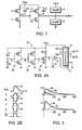
- FIG. 1is a circuit showing the prior art circuitry and its limitations
- FIG. 2Ais a circuit schematic example illustrating the present invention
- FIG. 2Bis a time graph of signals associated with FIG. 2A ;
- FIG. 3illustrates charts of ESD voltage stress current sharing of the prior art protection and the protection of the present invention.
- FIG. 2Ashows a circuit schematic of a particular example illustrating the present invention.
- a buffer 20is an output driver that transfers logic input signals (IN 1 -INn) to the outputs (OUT 1 -OUTn).
- the buffer 20has a low true OE 22 signal that will set the output transistors into a three state condition regardless of the logic inputs.
- the power rail Vddis coupled from the buffer 20 to the ESD protective circuit 24 .
- the width of the signals, B, C, Dare arranged to be about 200 nanoseconds, but other times may be used.
- the capacitoris typically a reversed biased diode, and the values of the C and the R are best selected via simulations. Size tradeoffs between the C and the R, and other tradeoffs that might exist for particular applications, will be understood by those skilled in the art.
- FIG. 3shows two graphs illustrating the advantage of the present invention.
- Trace 50peaks at about 900 mA and represents the current in the buffer output NMOS when the present invention is not employed.
- the circuitdid have the prior art primary ESD clamps tied to the output node itself.
- the trace 52represents the current in the primary ESD device. This current peaks at about 250 mA.
- the output NMOSis at risk.
- Trace 54represents the current in the primary ESD device when the present invention is used.
- the currentpeaks at about 1.2 A, and there is no current 56 in the output NMOS.
- Experiments conductedshow that the output pin's ESD stress tolerance increased from 1 kV to 4 kV.
- the present inventionis discussed herein about protecting the output NMOS pull down transistor.
- the PMOSis also protected as driving the OE false will also ensure that the PMOS is off. This might be important in applications where the ESD event is a negative spike.
- the primary protection for negative spikesmay be the Merrill circuit or often it is a diode from Vss to +Vdd, where the diode conducts forward when +Vdd falls below the Vss level. The above is well known to those in the field.
- the primary ESD protectionmay be tied to the buffer outputs, and the present invention will assure that these primary devices will substantially bear the ESD stress.
- the primary ESD protection devicesmay be attached between the +Vdd and Vss rails near or at the buffer chip/package.
- the present inventionmay be applied to any circuit susceptible to ESD stresses, especially those with an OE control or similar control input.
- the present inventionmay be applied to other circuits to protect pull up transistors as well as pull down transistors.
Landscapes
- Semiconductor Integrated Circuits (AREA)
Abstract
Description
- 1. Field of the Invention
- The present invention relates to electro-static discharge (ESD) protection circuits for integrated circuits, and more particularly ESD protection of an integrated circuit's output MOS transistors.
- 2. Background Information
- As integrated circuits (ICs), especially CMOS circuits, are reduced in size into the sub-micron range with ever thinner oxide layers, shallower junctions, more lightly doped structures, and silicided diffusions, the structures become ever more susceptible to ESD induced failures. Human and/or mechanical handling produces static charges that can and do cause destructive failure in such ICs. The components most at risk of such a failure are those that are electrically connected to output terminals or pads leading off the printed circuit board that carry the components. It has been found that human body ESD stress will damage an output NMOS even though there is a primary ESD protection cell located on the NMOS.
- ESD voltage stress, event, ESD voltage spike or voltage stress is understood in the art as being interchangeable.
- Generally, ESD voltage stresses produce voltages that permanently damage thin oxide insulting layers and/or uneven current densities that damage junctions and/or diffusion profiles in small areas. These mechanisms have been well documented in the art. For example, see “Achieving Uniform NMOS Device Power Distribution for Sub-micron ESD Reliability,” by C. Duvvury, C. Diaz, and T. Haddock, in IEDMTechnical Digest, 1992.
- Prior art ESD protect circuits include series resistors, filter capacitors, clamp diodes and Zeners or other such breakdown devices employed at the terminals to limit the effect of the ESD event. These protection techniques are designed, inter alia, with marginal success to trigger at ESD voltages higher than the typical operating voltages of the product itself, so that the ESD protection does not interfere with the typical product functional operation.
- The problem is that an ESD event at an output, where the output has an NMOS to Vss, or ground and a PMOS to a power rail, Vdd, couples through the PMOS capacitor to the Vdd rail and through the logic circuitry involved to turn on the NMOS. The NMOS discharges the ESD event and prevents primary ESD protection devices from operating fully, if at all. More troublesome is that as the NMOS is turning on, it may enter a “snap-back” condition (well known in the art) where parasitic bipolar transistors may turn on. In such conditions the output NMOS often will fail or be substantially weakened so as to exhibit increase leakage after the ESD stress is removed. Such components may fail in the field, which is worse.
FIG. 1 illustrates the operation. Even withclamps 10 on the output, the NMOS N1 may turn on. Theclamp 10 is shown generically. A positive going voltage spike on the OUTPUT, say by a human touching it, is coupled through the output capacitances C1 and C2 of the PMOS's P1 and P2 to the gate of N1. There is nothing to prevent N1 from turning on and reducing the voltage spike. Reducing the voltage spike may interfere with the primary ESD protection device, theclamps 10, or any protective circuits attached directly to the +Vdd line from fully activating. As discussed later, in fact, the NMOS N1 and theclamps 10 will share discharging the voltage spike, but the issue is that N1 is susceptible to failure. - U.S. Pat. No. 5,239,440 to Merrill addresses such an issue. Merrill provides a single RC detection circuit to actively turn on protective MOS switches attached to each output. On each output there is a transistor switch to Vcc and one to Vss (one to power and one to ground). Depending on the polarity of the ESD event, the proper switch is activated.
- The prior art circuits have a number of limitations that are directly addressed by the present invention. Among those limitations is that the pull down NMOS on the output still may turn on, regardless of the switches or clamps on the output node. Moreover, the switches on each output provide a connection between each output (for example when the switches are not activated) that may allow transients to cause noise in adjacent output even with the low impedance Vcc or ground connections. Another significant limitation is that the two switches (as in the Merrill “clamp”) on each output occupy valuable chip area.
- The present invention provides protection for target circuits with output transistor drivers from an ESD voltage stress without making direct contact with the output nodes. It is efficient of chip area, and it protects better by ensuring the output transistors remain off during an ESD voltage stress or similar event.
- Many (or most) output buffer circuits or logic circuits have output driver transistors that connect to output nodes or terminals. Many of these are integrated circuits, IC's, that have output enable functions. Typically such circuits have outputs that are called “three state.” The outputs may be logically high, low or floating (open circuited). In these circuits, a logic input is directed through circuitry to cause output transistors to turn on or off thereby driving the output high or low (a one or a zero logic state). In addition, when the output enable, or OE, is false, the OE dominates the logic signal and the output transistors are securely forced off (usually there are two output MOS transistors per output node—a pull up and a pull down). In such a condition, the output node is left floating, this floating condition being the third state. The OE signal typically is connected within the IC directly or nearly directly to the output transistors.
- Often a group of output buffer circuits are contained in a single chip or package with a single common OE connection that runs to all the actual output transistors. The chip or package has a single (usually) +Vdd power rail and a ground (Vss) connection. The present invention provides ESD protection from an ESD voltage stress that occurs on the target circuit output node. The ESD voltage stress is transferred to the +Vdd power rail in the target IC via the output pull up transistor. The present invention has a detection circuit that receives an ESD voltage stress directly from the +Vdd power rail and transfers it through a capacitor to the input of an inverter. The capacitor also connects to a resistor to ground, the RC combination forming a differentiation circuit with a characteristic time constant. The voltage stress activates the inverter when its threshold is reached. The inverter will remain active until the RC charges the capacitor such that the inverter input falls below the threshold. The output of the inverter is a logic timed square wave. The inverter output is fed through circuitry and is combined or gated with the usual OE signal so that during an ESD voltage stress, the OE input to the output circuit is false, and the output transistors are off. In preferred embodiments, the gating may be a NAND, NOR, AND, OR or wired OR depending on the actual application.
- The present invention provides an ESD protection circuit that drives the OE input of an integrated or other circuit. Since the OE signal typically controls at least a byte or as much as a full word that may contain thirty-two, sixty-four or even more bits, a single inventive ESD circuit, with no physical connection to the output nodes, can protect all the output driver transistors.
- The invention description below refers to the accompanying drawings, of which:
FIG. 1 is a circuit showing the prior art circuitry and its limitations;FIG. 2A is a circuit schematic example illustrating the present invention;FIG. 2B is a time graph of signals associated withFIG. 2A ;FIG. 3 illustrates charts of ESD voltage stress current sharing of the prior art protection and the protection of the present invention.FIG. 2A shows a circuit schematic of a particular example illustrating the present invention. Here abuffer 20 is an output driver that transfers logic input signals (IN1-INn) to the outputs (OUT1-OUTn). Thebuffer 20 has a lowtrue OE 22 signal that will set the output transistors into a three state condition regardless of the logic inputs. The power rail Vdd is coupled from thebuffer 20 to the ESDprotective circuit 24.- As shown in
FIG. 2B , when an ESD positive goingvoltage spike 26 occurs, that spike26 transfers a signal across the capacitor C to point A. Point A rises28 in response and then, depending on the RC, and the edges of the ESD voltage spike, the RC will act to differentiate theES signal 26. Point A rises passing the threshold of theinverter 30 causing a low goinglogic level signal 32 at point B. This in turn is inverted by theinverter 34 to form the high goinglogic signal 36 at point C. The signal at point C turns on NMOS N2 causing the logic signal38 at point D to go low. This low at point D via theNAND gate 40 forces theoutput 22 of theNAND 40 to go high. Since this output is the low true OE signal into thebuffer 20, the buffer is forced into a three state condition, and the output NMOS transistors in each of the output circuits are held off. - In a preferred embodiment, the width of the signals, B, C, D are arranged to be about 200 nanoseconds, but other times may be used. The capacitor is typically a reversed biased diode, and the values of the C and the R are best selected via simulations. Size tradeoffs between the C and the R, and other tradeoffs that might exist for particular applications, will be understood by those skilled in the art.
- As shown in
FIG. 2A , theNAND gate 40 in routine operations transfers a hightrue OE signal 42 to the lowtrue OE signal 22. In the absence of any ESD voltage spike, point D is held low andNAND 40 acts only to invert the output enable signal on its way to thebuffer 20. FIG. 3 shows two graphs illustrating the advantage of the present invention.Trace 50 peaks at about 900 mA and represents the current in the buffer output NMOS when the present invention is not employed. The circuit did have the prior art primary ESD clamps tied to the output node itself. At this time thetrace 52 represents the current in the primary ESD device. This current peaks at about 250 mA. Clearly, the output NMOS is at risk.Trace 54 represents the current in the primary ESD device when the present invention is used. Here the current peaks at about 1.2 A, and there is no current56 in the output NMOS. Experiments conducted show that the output pin's ESD stress tolerance increased from 1 kV to 4 kV.- There is usually a PMOS pull up transistor in the buffer outputs. The present invention is discussed herein about protecting the output NMOS pull down transistor. However, the PMOS is also protected as driving the OE false will also ensure that the PMOS is off. This might be important in applications where the ESD event is a negative spike. The primary protection for negative spikes may be the Merrill circuit or often it is a diode from Vss to +Vdd, where the diode conducts forward when +Vdd falls below the Vss level. The above is well known to those in the field.
- There are indications that snap-back conditions exist in the NMOS circuit without the present invention resulting in leakage after the ESD stress is removed. The circuit with the present invention shows no snap-back and no leakage.
- In practice, the primary ESD protection may be tied to the buffer outputs, and the present invention will assure that these primary devices will substantially bear the ESD stress. However, using the present invention, the primary ESD protection devices may be attached between the +Vdd and Vss rails near or at the buffer chip/package. Of course the present invention may be applied to any circuit susceptible to ESD stresses, especially those with an OE control or similar control input.
- Note that the closer the OE control input is to the output driving transistors, the more effective the protection will be. If there is substantial circuitry between the output transistor and the OE signal, the efficiency of the present invention will diminish.
- Also, the present invention may be applied to other circuits to protect pull up transistors as well as pull down transistors.
Claims (14)
Priority Applications (1)
| Application Number | Priority Date | Filing Date | Title |
|---|---|---|---|
| US11/261,812US8254069B2 (en) | 2005-10-28 | 2005-10-28 | ESD protection for outputs |
Applications Claiming Priority (1)
| Application Number | Priority Date | Filing Date | Title |
|---|---|---|---|
| US11/261,812US8254069B2 (en) | 2005-10-28 | 2005-10-28 | ESD protection for outputs |
Publications (2)
| Publication Number | Publication Date |
|---|---|
| US20070097568A1true US20070097568A1 (en) | 2007-05-03 |
| US8254069B2 US8254069B2 (en) | 2012-08-28 |
Family
ID=37995962
Family Applications (1)
| Application Number | Title | Priority Date | Filing Date |
|---|---|---|---|
| US11/261,812Active2027-06-15US8254069B2 (en) | 2005-10-28 | 2005-10-28 | ESD protection for outputs |
Country Status (1)
| Country | Link |
|---|---|
| US (1) | US8254069B2 (en) |
Cited By (7)
| Publication number | Priority date | Publication date | Assignee | Title |
|---|---|---|---|---|
| US20070025033A1 (en)* | 2005-07-28 | 2007-02-01 | Oki Electric Industry Co., Ltd. | Semiconductor device |
| US20090187361A1 (en)* | 2008-01-23 | 2009-07-23 | Himax Technologies Limited | Transient detection circuit for esd protection |
| CN103036220A (en)* | 2012-04-28 | 2013-04-10 | 上海华虹Nec电子有限公司 | Electro spark detector (ESD) circuit protection structure |
| US9136690B1 (en)* | 2011-08-30 | 2015-09-15 | Xilinx, Inc. | Front-end circuit with electro-static discharge protection |
| US20180041233A1 (en)* | 2015-03-17 | 2018-02-08 | Renesas Electronics Corporation | Transmitter circuit, semiconductor apparatus and data transmission method |
| CN110391650A (en)* | 2018-04-18 | 2019-10-29 | 力旺电子股份有限公司 | Electrostatic Discharge Circuit |
| KR20240008382A (en)* | 2021-07-08 | 2024-01-18 | 퀄컴 인코포레이티드 | Interface circuit with robust electrostatic discharge |
Citations (9)
| Publication number | Priority date | Publication date | Assignee | Title |
|---|---|---|---|---|
| US4855620A (en)* | 1987-11-18 | 1989-08-08 | Texas Instruments Incorporated | Output buffer with improved ESD protection |
| US5239440A (en)* | 1989-12-19 | 1993-08-24 | National Semiconductor Corporation | Electrostatic discharge protection for integrated circuits |
| US5946175A (en)* | 1998-02-17 | 1999-08-31 | Winbond Electronics Corp. | Secondary ESD/EOS protection circuit |
| US6118323A (en)* | 1997-01-10 | 2000-09-12 | Texas Instruments Incorporated | Electrostatic discharge protection circuit and method |
| US6385021B1 (en)* | 2000-04-10 | 2002-05-07 | Motorola, Inc. | Electrostatic discharge (ESD) protection circuit |
| US20020140489A1 (en)* | 2001-03-28 | 2002-10-03 | Maloney Timothy J. | Method and apparatus for electro-static discharge protection |
| US20030016062A1 (en)* | 2001-07-23 | 2003-01-23 | Zahid Ahsanullah | Controlling signal states and leakage current during a sleep mode |
| US20040136126A1 (en)* | 2003-01-10 | 2004-07-15 | Smith Jeremy C. | Electrostatic discharge protection circuit with feedback enhanced triggering |
| US20050046443A1 (en)* | 2003-09-02 | 2005-03-03 | Mccalmont Jonathan S. | Input terminal with combined logic threshold and reset function |
- 2005
- 2005-10-28USUS11/261,812patent/US8254069B2/enactiveActive
Patent Citations (9)
| Publication number | Priority date | Publication date | Assignee | Title |
|---|---|---|---|---|
| US4855620A (en)* | 1987-11-18 | 1989-08-08 | Texas Instruments Incorporated | Output buffer with improved ESD protection |
| US5239440A (en)* | 1989-12-19 | 1993-08-24 | National Semiconductor Corporation | Electrostatic discharge protection for integrated circuits |
| US6118323A (en)* | 1997-01-10 | 2000-09-12 | Texas Instruments Incorporated | Electrostatic discharge protection circuit and method |
| US5946175A (en)* | 1998-02-17 | 1999-08-31 | Winbond Electronics Corp. | Secondary ESD/EOS protection circuit |
| US6385021B1 (en)* | 2000-04-10 | 2002-05-07 | Motorola, Inc. | Electrostatic discharge (ESD) protection circuit |
| US20020140489A1 (en)* | 2001-03-28 | 2002-10-03 | Maloney Timothy J. | Method and apparatus for electro-static discharge protection |
| US20030016062A1 (en)* | 2001-07-23 | 2003-01-23 | Zahid Ahsanullah | Controlling signal states and leakage current during a sleep mode |
| US20040136126A1 (en)* | 2003-01-10 | 2004-07-15 | Smith Jeremy C. | Electrostatic discharge protection circuit with feedback enhanced triggering |
| US20050046443A1 (en)* | 2003-09-02 | 2005-03-03 | Mccalmont Jonathan S. | Input terminal with combined logic threshold and reset function |
Cited By (12)
| Publication number | Priority date | Publication date | Assignee | Title |
|---|---|---|---|---|
| US20070025033A1 (en)* | 2005-07-28 | 2007-02-01 | Oki Electric Industry Co., Ltd. | Semiconductor device |
| US7489486B2 (en)* | 2005-07-28 | 2009-02-10 | Oki Electric Industry Co., Ltd. | Semiconductor device |
| US20090187361A1 (en)* | 2008-01-23 | 2009-07-23 | Himax Technologies Limited | Transient detection circuit for esd protection |
| US7710696B2 (en)* | 2008-01-23 | 2010-05-04 | Himax Technologies Limited | Transient detection circuit for ESD protection |
| CN101493489B (en)* | 2008-01-23 | 2011-08-31 | 奇景光电股份有限公司 | Transient detection circuit and integrated circuit |
| US9136690B1 (en)* | 2011-08-30 | 2015-09-15 | Xilinx, Inc. | Front-end circuit with electro-static discharge protection |
| CN103036220A (en)* | 2012-04-28 | 2013-04-10 | 上海华虹Nec电子有限公司 | Electro spark detector (ESD) circuit protection structure |
| US20180041233A1 (en)* | 2015-03-17 | 2018-02-08 | Renesas Electronics Corporation | Transmitter circuit, semiconductor apparatus and data transmission method |
| US10224969B2 (en)* | 2015-03-17 | 2019-03-05 | Renesas Electronics Corporation | Transmitter circuit, semiconductor apparatus and data transmission method |
| CN110391650A (en)* | 2018-04-18 | 2019-10-29 | 力旺电子股份有限公司 | Electrostatic Discharge Circuit |
| KR20240008382A (en)* | 2021-07-08 | 2024-01-18 | 퀄컴 인코포레이티드 | Interface circuit with robust electrostatic discharge |
| KR102648775B1 (en) | 2021-07-08 | 2024-03-15 | 퀄컴 인코포레이티드 | Interface circuit with robust electrostatic discharge |
Also Published As
| Publication number | Publication date |
|---|---|
| US8254069B2 (en) | 2012-08-28 |
Similar Documents
| Publication | Publication Date | Title |
|---|---|---|
| US7839613B2 (en) | Electrostatic discharge protection circuit protecting thin gate insulation layers in a semiconductor device | |
| US5946175A (en) | Secondary ESD/EOS protection circuit | |
| US7304827B2 (en) | ESD protection circuits for mixed-voltage buffers | |
| US8315024B2 (en) | Electrostatic discharge protection circuit, integrated circuit and method of protecting circuitry from an electrostatic discharge voltage | |
| US7656627B2 (en) | ESD protection circuit with active triggering | |
| US6867957B1 (en) | Stacked-NMOS-triggered SCR device for ESD-protection | |
| CN102738782B (en) | The esd protection circuit of semiconductor integrated circuit | |
| US7307822B2 (en) | Semiconductor integrated circuit apparatus | |
| US6927957B1 (en) | Electrostatic discharge clamp | |
| US20090040668A1 (en) | Esd protection circuits for mixed-voltage buffers | |
| US8050003B2 (en) | Electrostatic discharge protection circuit having a reduced size and lower operating voltage | |
| EP1208627A1 (en) | Circuits for dynamic turn off of nmos output drivers during eos/esd stress | |
| US10158225B2 (en) | ESD protection system utilizing gate-floating scheme and control circuit thereof | |
| US7672103B2 (en) | Circuit having low operating voltage for protecting semiconductor device from electrostatic discharge | |
| US20200243512A1 (en) | Nmos transistor with bulk dynamically coupled to drain | |
| KR100688531B1 (en) | I / O circuit with stable high voltage immunity against electrostatic voltage | |
| JP2006100606A (en) | Semiconductor device | |
| US8254069B2 (en) | ESD protection for outputs | |
| US6757147B1 (en) | Pin-to-pin ESD-protection structure having cross-pin activation | |
| KR20060099464A (en) | Electrostatic Protection Devices for Semiconductor Devices | |
| US6738242B1 (en) | ESD-isolation circuit driving gate of bus-switch transistor during ESD pulse between two I/O pins | |
| KR100587089B1 (en) | Electrostatic Protection Devices for Semiconductor Devices | |
| US20070247771A1 (en) | Analog Input/Output Circuit with ESD Protection | |
| JP2004022950A (en) | Circuit for preventing electrostatic breakdown of semiconductor devices | |
| US7362555B2 (en) | ESD protection circuit for a mixed-voltage semiconductor device |
Legal Events
| Date | Code | Title | Description |
|---|---|---|---|
| FEPP | Fee payment procedure | Free format text:PAYOR NUMBER ASSIGNED (ORIGINAL EVENT CODE: ASPN); ENTITY STATUS OF PATENT OWNER: LARGE ENTITY | |
| AS | Assignment | Owner name:FAIRCHILD SEMICONDUCTOR CORPORATION, CALIFORNIA Free format text:ASSIGNMENT OF ASSIGNORS INTEREST;ASSIGNOR:MISKE, MYRON J.;REEL/FRAME:028292/0981 Effective date:20120521 | |
| STCF | Information on status: patent grant | Free format text:PATENTED CASE | |
| FPAY | Fee payment | Year of fee payment:4 | |
| AS | Assignment | Owner name:DEUTSCHE BANK AG NEW YORK BRANCH, AS COLLATERAL AGENT, NEW YORK Free format text:PATENT SECURITY AGREEMENT;ASSIGNOR:FAIRCHILD SEMICONDUCTOR CORPORATION;REEL/FRAME:040075/0644 Effective date:20160916 Owner name:DEUTSCHE BANK AG NEW YORK BRANCH, AS COLLATERAL AG Free format text:PATENT SECURITY AGREEMENT;ASSIGNOR:FAIRCHILD SEMICONDUCTOR CORPORATION;REEL/FRAME:040075/0644 Effective date:20160916 | |
| MAFP | Maintenance fee payment | Free format text:PAYMENT OF MAINTENANCE FEE, 8TH YEAR, LARGE ENTITY (ORIGINAL EVENT CODE: M1552); ENTITY STATUS OF PATENT OWNER: LARGE ENTITY Year of fee payment:8 | |
| AS | Assignment | Owner name:SEMICONDUCTOR COMPONENTS INDUSTRIES, LLC, ARIZONA Free format text:ASSIGNMENT OF ASSIGNORS INTEREST;ASSIGNOR:FAIRCHILD SEMICONDUCTOR CORPORATION;REEL/FRAME:057694/0374 Effective date:20210722 | |
| AS | Assignment | Owner name:FAIRCHILD SEMICONDUCTOR CORPORATION, ARIZONA Free format text:RELEASE BY SECURED PARTY;ASSIGNOR:DEUTSCHE BANK AG NEW YORK BRANCH;REEL/FRAME:057969/0206 Effective date:20211027 | |
| AS | Assignment | Owner name:DEUTSCHE BANK AG NEW YORK BRANCH, AS COLLATERAL AGENT, NEW YORK Free format text:SECURITY INTEREST;ASSIGNOR:SEMICONDUCTOR COMPONENTS INDUSTRIES, LLC;REEL/FRAME:058871/0799 Effective date:20211028 | |
| AS | Assignment | Owner name:FAIRCHILD SEMICONDUCTOR CORPORATION, ARIZONA Free format text:RELEASE OF SECURITY INTEREST IN PATENTS RECORDED AT REEL 040075, FRAME 0644;ASSIGNOR:DEUTSCHE BANK AG NEW YORK BRANCH, AS COLLATERAL AGENT;REEL/FRAME:064070/0536 Effective date:20230622 Owner name:SEMICONDUCTOR COMPONENTS INDUSTRIES, LLC, ARIZONA Free format text:RELEASE OF SECURITY INTEREST IN PATENTS RECORDED AT REEL 040075, FRAME 0644;ASSIGNOR:DEUTSCHE BANK AG NEW YORK BRANCH, AS COLLATERAL AGENT;REEL/FRAME:064070/0536 Effective date:20230622 | |
| AS | Assignment | Owner name:FAIRCHILD SEMICONDUCTOR CORPORATION, ARIZONA Free format text:RELEASE OF SECURITY INTEREST IN PATENTS RECORDED AT REEL 058871, FRAME 0799;ASSIGNOR:DEUTSCHE BANK AG NEW YORK BRANCH, AS COLLATERAL AGENT;REEL/FRAME:065653/0001 Effective date:20230622 Owner name:SEMICONDUCTOR COMPONENTS INDUSTRIES, LLC, ARIZONA Free format text:RELEASE OF SECURITY INTEREST IN PATENTS RECORDED AT REEL 058871, FRAME 0799;ASSIGNOR:DEUTSCHE BANK AG NEW YORK BRANCH, AS COLLATERAL AGENT;REEL/FRAME:065653/0001 Effective date:20230622 | |
| MAFP | Maintenance fee payment | Free format text:PAYMENT OF MAINTENANCE FEE, 12TH YEAR, LARGE ENTITY (ORIGINAL EVENT CODE: M1553); ENTITY STATUS OF PATENT OWNER: LARGE ENTITY Year of fee payment:12 |