US20070096279A1 - Protecting structure and manufacturing method for electronic packaging contacts - Google Patents
Protecting structure and manufacturing method for electronic packaging contactsDownload PDFInfo
- Publication number
- US20070096279A1 US20070096279A1US11/516,944US51694406AUS2007096279A1US 20070096279 A1US20070096279 A1US 20070096279A1US 51694406 AUS51694406 AUS 51694406AUS 2007096279 A1US2007096279 A1US 2007096279A1
- Authority
- US
- United States
- Prior art keywords
- chip
- protecting
- protecting layer
- conductor trace
- trace line
- Prior art date
- Legal status (The legal status is an assumption and is not a legal conclusion. Google has not performed a legal analysis and makes no representation as to the accuracy of the status listed.)
- Granted
Links
- 238000004519manufacturing processMethods0.000titleclaimsabstractdescription11
- 238000004100electronic packagingMethods0.000titleclaims4
- 239000004020conductorSubstances0.000claimsabstractdescription39
- 238000000034methodMethods0.000claimsabstractdescription18
- 238000000151depositionMethods0.000claimsabstractdescription7
- 238000007639printingMethods0.000claimsabstractdescription7
- 239000011248coating agentSubstances0.000claimsabstractdescription6
- 238000000576coating methodMethods0.000claimsabstractdescription6
- 239000000758substrateSubstances0.000claimsdescription19
- 239000000463materialSubstances0.000claimsdescription7
- 229920002521macromoleculePolymers0.000claimsdescription4
- 238000005553drillingMethods0.000claimsdescription2
- 238000001312dry etchingMethods0.000claimsdescription2
- 238000009713electroplatingMethods0.000claimsdescription2
- 239000002184metalSubstances0.000claimsdescription2
- 238000009987spinningMethods0.000claimsdescription2
- 238000001039wet etchingMethods0.000claimsdescription2
- 238000000206photolithographyMethods0.000claims1
- 239000010410layerSubstances0.000abstract1
- 239000011241protective layerSubstances0.000abstract1
- 238000004806packaging method and processMethods0.000description18
- 239000004065semiconductorSubstances0.000description13
- 238000004088simulationMethods0.000description10
- 238000005516engineering processMethods0.000description4
- 238000004377microelectronicMethods0.000description4
- 238000004458analytical methodMethods0.000description2
- 238000012986modificationMethods0.000description2
- 230000004048modificationEffects0.000description2
- 230000001681protective effectEffects0.000description2
- 239000004642PolyimideSubstances0.000description1
- 230000005540biological transmissionEffects0.000description1
- 238000011109contaminationMethods0.000description1
- 230000002708enhancing effectEffects0.000description1
- 230000001788irregularEffects0.000description1
- 238000000465mouldingMethods0.000description1
- 229920001721polyimidePolymers0.000description1
Images


Classifications
- H—ELECTRICITY
- H01—ELECTRIC ELEMENTS
- H01L—SEMICONDUCTOR DEVICES NOT COVERED BY CLASS H10
- H01L23/00—Details of semiconductor or other solid state devices
- H01L23/52—Arrangements for conducting electric current within the device in operation from one component to another, i.e. interconnections, e.g. wires, lead frames
- H01L23/538—Arrangements for conducting electric current within the device in operation from one component to another, i.e. interconnections, e.g. wires, lead frames the interconnection structure between a plurality of semiconductor chips being formed on, or in, insulating substrates
- H01L23/5389—Arrangements for conducting electric current within the device in operation from one component to another, i.e. interconnections, e.g. wires, lead frames the interconnection structure between a plurality of semiconductor chips being formed on, or in, insulating substrates the chips being integrally enclosed by the interconnect and support structures
- H—ELECTRICITY
- H01—ELECTRIC ELEMENTS
- H01L—SEMICONDUCTOR DEVICES NOT COVERED BY CLASS H10
- H01L24/00—Arrangements for connecting or disconnecting semiconductor or solid-state bodies; Methods or apparatus related thereto
- H01L24/01—Means for bonding being attached to, or being formed on, the surface to be connected, e.g. chip-to-package, die-attach, "first-level" interconnects; Manufacturing methods related thereto
- H01L24/18—High density interconnect [HDI] connectors; Manufacturing methods related thereto
- H01L24/19—Manufacturing methods of high density interconnect preforms
- H—ELECTRICITY
- H01—ELECTRIC ELEMENTS
- H01L—SEMICONDUCTOR DEVICES NOT COVERED BY CLASS H10
- H01L24/00—Arrangements for connecting or disconnecting semiconductor or solid-state bodies; Methods or apparatus related thereto
- H01L24/01—Means for bonding being attached to, or being formed on, the surface to be connected, e.g. chip-to-package, die-attach, "first-level" interconnects; Manufacturing methods related thereto
- H01L24/18—High density interconnect [HDI] connectors; Manufacturing methods related thereto
- H01L24/23—Structure, shape, material or disposition of the high density interconnect connectors after the connecting process
- H01L24/24—Structure, shape, material or disposition of the high density interconnect connectors after the connecting process of an individual high density interconnect connector
- H—ELECTRICITY
- H01—ELECTRIC ELEMENTS
- H01L—SEMICONDUCTOR DEVICES NOT COVERED BY CLASS H10
- H01L24/00—Arrangements for connecting or disconnecting semiconductor or solid-state bodies; Methods or apparatus related thereto
- H01L24/80—Methods for connecting semiconductor or other solid state bodies using means for bonding being attached to, or being formed on, the surface to be connected
- H01L24/82—Methods for connecting semiconductor or other solid state bodies using means for bonding being attached to, or being formed on, the surface to be connected by forming build-up interconnects at chip-level, e.g. for high density interconnects [HDI]
- H—ELECTRICITY
- H01—ELECTRIC ELEMENTS
- H01L—SEMICONDUCTOR DEVICES NOT COVERED BY CLASS H10
- H01L2224/00—Indexing scheme for arrangements for connecting or disconnecting semiconductor or solid-state bodies and methods related thereto as covered by H01L24/00
- H01L2224/01—Means for bonding being attached to, or being formed on, the surface to be connected, e.g. chip-to-package, die-attach, "first-level" interconnects; Manufacturing methods related thereto
- H01L2224/18—High density interconnect [HDI] connectors; Manufacturing methods related thereto
- H01L2224/23—Structure, shape, material or disposition of the high density interconnect connectors after the connecting process
- H01L2224/24—Structure, shape, material or disposition of the high density interconnect connectors after the connecting process of an individual high density interconnect connector
- H01L2224/241—Disposition
- H01L2224/24151—Connecting between a semiconductor or solid-state body and an item not being a semiconductor or solid-state body, e.g. chip-to-substrate, chip-to-passive
- H01L2224/24221—Connecting between a semiconductor or solid-state body and an item not being a semiconductor or solid-state body, e.g. chip-to-substrate, chip-to-passive the body and the item being stacked
- H01L2224/24225—Connecting between a semiconductor or solid-state body and an item not being a semiconductor or solid-state body, e.g. chip-to-substrate, chip-to-passive the body and the item being stacked the item being non-metallic, e.g. insulating substrate with or without metallisation
- H01L2224/24227—Connecting between a semiconductor or solid-state body and an item not being a semiconductor or solid-state body, e.g. chip-to-substrate, chip-to-passive the body and the item being stacked the item being non-metallic, e.g. insulating substrate with or without metallisation the HDI interconnect not connecting to the same level of the item at which the semiconductor or solid-state body is mounted, e.g. the semiconductor or solid-state body being mounted in a cavity or on a protrusion of the item
- H—ELECTRICITY
- H01—ELECTRIC ELEMENTS
- H01L—SEMICONDUCTOR DEVICES NOT COVERED BY CLASS H10
- H01L2224/00—Indexing scheme for arrangements for connecting or disconnecting semiconductor or solid-state bodies and methods related thereto as covered by H01L24/00
- H01L2224/80—Methods for connecting semiconductor or other solid state bodies using means for bonding being attached to, or being formed on, the surface to be connected
- H01L2224/82—Methods for connecting semiconductor or other solid state bodies using means for bonding being attached to, or being formed on, the surface to be connected by forming build-up interconnects at chip-level, e.g. for high density interconnects [HDI]
- H01L2224/82009—Pre-treatment of the connector or the bonding area
- H01L2224/8203—Reshaping, e.g. forming vias
- H01L2224/82035—Reshaping, e.g. forming vias by heating means
- H01L2224/82039—Reshaping, e.g. forming vias by heating means using a laser
- H—ELECTRICITY
- H01—ELECTRIC ELEMENTS
- H01L—SEMICONDUCTOR DEVICES NOT COVERED BY CLASS H10
- H01L23/00—Details of semiconductor or other solid state devices
- H01L23/28—Encapsulations, e.g. encapsulating layers, coatings, e.g. for protection
- H01L23/31—Encapsulations, e.g. encapsulating layers, coatings, e.g. for protection characterised by the arrangement or shape
- H01L23/3107—Encapsulations, e.g. encapsulating layers, coatings, e.g. for protection characterised by the arrangement or shape the device being completely enclosed
- H01L23/3121—Encapsulations, e.g. encapsulating layers, coatings, e.g. for protection characterised by the arrangement or shape the device being completely enclosed a substrate forming part of the encapsulation
- H01L23/3128—Encapsulations, e.g. encapsulating layers, coatings, e.g. for protection characterised by the arrangement or shape the device being completely enclosed a substrate forming part of the encapsulation the substrate having spherical bumps for external connection
- H—ELECTRICITY
- H01—ELECTRIC ELEMENTS
- H01L—SEMICONDUCTOR DEVICES NOT COVERED BY CLASS H10
- H01L2924/00—Indexing scheme for arrangements or methods for connecting or disconnecting semiconductor or solid-state bodies as covered by H01L24/00
- H01L2924/01—Chemical elements
- H01L2924/01005—Boron [B]
- H—ELECTRICITY
- H01—ELECTRIC ELEMENTS
- H01L—SEMICONDUCTOR DEVICES NOT COVERED BY CLASS H10
- H01L2924/00—Indexing scheme for arrangements or methods for connecting or disconnecting semiconductor or solid-state bodies as covered by H01L24/00
- H01L2924/01—Chemical elements
- H01L2924/01006—Carbon [C]
- H—ELECTRICITY
- H01—ELECTRIC ELEMENTS
- H01L—SEMICONDUCTOR DEVICES NOT COVERED BY CLASS H10
- H01L2924/00—Indexing scheme for arrangements or methods for connecting or disconnecting semiconductor or solid-state bodies as covered by H01L24/00
- H01L2924/01—Chemical elements
- H01L2924/01033—Arsenic [As]
- H—ELECTRICITY
- H01—ELECTRIC ELEMENTS
- H01L—SEMICONDUCTOR DEVICES NOT COVERED BY CLASS H10
- H01L2924/00—Indexing scheme for arrangements or methods for connecting or disconnecting semiconductor or solid-state bodies as covered by H01L24/00
- H01L2924/10—Details of semiconductor or other solid state devices to be connected
- H01L2924/11—Device type
- H01L2924/14—Integrated circuits
- H—ELECTRICITY
- H01—ELECTRIC ELEMENTS
- H01L—SEMICONDUCTOR DEVICES NOT COVERED BY CLASS H10
- H01L2924/00—Indexing scheme for arrangements or methods for connecting or disconnecting semiconductor or solid-state bodies as covered by H01L24/00
- H01L2924/15—Details of package parts other than the semiconductor or other solid state devices to be connected
- H01L2924/151—Die mounting substrate
- H01L2924/1515—Shape
- H01L2924/15153—Shape the die mounting substrate comprising a recess for hosting the device
- H—ELECTRICITY
- H01—ELECTRIC ELEMENTS
- H01L—SEMICONDUCTOR DEVICES NOT COVERED BY CLASS H10
- H01L2924/00—Indexing scheme for arrangements or methods for connecting or disconnecting semiconductor or solid-state bodies as covered by H01L24/00
- H01L2924/15—Details of package parts other than the semiconductor or other solid state devices to be connected
- H01L2924/151—Die mounting substrate
- H01L2924/15165—Monolayer substrate
- H—ELECTRICITY
- H01—ELECTRIC ELEMENTS
- H01L—SEMICONDUCTOR DEVICES NOT COVERED BY CLASS H10
- H01L2924/00—Indexing scheme for arrangements or methods for connecting or disconnecting semiconductor or solid-state bodies as covered by H01L24/00
- H01L2924/15—Details of package parts other than the semiconductor or other solid state devices to be connected
- H01L2924/151—Die mounting substrate
- H01L2924/153—Connection portion
- H01L2924/1531—Connection portion the connection portion being formed only on the surface of the substrate opposite to the die mounting surface
- H01L2924/15311—Connection portion the connection portion being formed only on the surface of the substrate opposite to the die mounting surface being a ball array, e.g. BGA
Definitions
- the present inventionrelates to an electronic package structure and the manufacturing method thereof, and more particularly to a structure for protecting electronic package contacts and the manufacturing method thereof.
- the U.S. Pat. No. 5,757,072disclosed that the protective cap 16 is used to cover the chip 12 a and the positive and passive components 12 which are sensible and easily interfered by exterior forces, in order to protect the overall manufacturing process from contamination within the high-density interconnecting structure 10 .
- the protective cap 16needs to be additionally manufactured and the structure thereof is quite complicated, and thus the cost therefor is high.
- the U.S. Pat. No. 6,586,836disclosed that the second die assembly 162 is used to reduce warpage of the microelectronic die, which prevents the microelectronic die from being disabled due to the gathering stress resulting from warpage.
- thisis only applied in the microelectronic dice with multiple chips.
- the techniqueis applied in limited fields and its procedures are more complicated.
- the U.S. Pat. No. 5,866,952disclosed that the compliant material 17 is deposited around the chips 14 and 20 , and then a mold form is positioned around the chips prior to molding a polymeric substrate therearound within the high-density interconnecting structure 26 .
- the chipis normally operated by preventing from the gathering stress thereon.
- the present inventionprovides a protecting structure.
- the protecting structureprotects conductor trace lines and via holes on the chip effectively to avoid the damage of the electronic terminal contacts or the broken conducting wires for rerouting, thereby enhancing the reliability of the conductor trace lines.
- a structure for protecting electronic package contactscomprises a chip, at least a dielectric layer, a conductor trace line and a protecting layer.
- the chiphas a plurality of electrodes and at least one dielectric layer covering the chip and the electrode.
- the conductor trace lineis mounted within the at least one dielectric layer and is in a lengthwise direction to connect electronic signals within the dielectric layer.
- the protecting layerat least covers a surrounding of the conductor trace line.
- the protecting layerhas a material of compressible macromolecules and the protecting layer covers the chip incompletely.
- the protecting layercovers the surrounding of the conductor trace line without contacting therewith.
- a protecting structure for electronic package contactscomprises a chip, a substrate, at least a dielectric layer, a conductor trace line and a protecting layer.
- the chiphas the plurality of electrodes.
- the substrateis mounted on one side of the chip and is used to support and distract heat form the chip.
- At least one dielectric layercovers the chips and the plurality of electrodes.
- the conductor trace lineis mounted within the dielectric layer and is in a lengthwise direction to connect electronic signals within the dielectric layer.
- the protecting layerat least covers the surrounding of the conductor trace line.
- the protecting layercovers the chips incompletely and the protecting layer covers the surrounding of the conductor trace line without contacting therewith.
- a manufacturing method for protecting electronic package contactscomprises the following steps of providing a chip having a plurality of electrodes; forming a protecting layer covering the chip and the plurality of electrodes; forming a dielectric layers covering the protecting layer and the chip; forming a via within the protecting and dielectric layers and forming a conductor trace line within the via.
- FIG. 1is a cross-section view of the chip covered with the protecting layer according to U.S. Pat. No. 5,757,072;
- FIG. 2is a cross-section view of the chip with the microelectronic die to reduce wargage of the embedded chip according to U.S. Pat. No. 6,866,952;
- FIG. 3is a cross-section view of the chip with the compliant material to reduce stresses according to U.S. Pat. No. 5,866,952;
- FIG. 4is a cross-section view of the stress simulation analysis model of the semiconductor component according to the present invention.
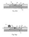
- FIG. 5is a cross-section view of the simulation result of the simulation structure without the protecting layer according to the present invention.
- FIG. 6is a cross-section view of the simulation result of the simulation structure with the protecting layer according to the present invention.
- FIG. 7shows the relationship between the thickness of the protecting layer and the quantity of stresses
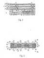
- FIGS. 8 ( a )- 8 ( g )are cross-section views of the manufacturing process for the packaging structure according to a first preferred embodiment of the present invention.
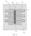
- FIG. 9is a vertical view of the packaging structure according to the first preferred embodiment of the present invention.
- FIG. 10is a cross-section view of the packaging structure according to a second preferred embodiment of the present invention.
- FIG. 11is a vertical view of the packaging structure according to the second preferred embodiment of the present invention.
- FIG. 12is a vertical view of the packaging structure according to a third preferred embodiment of the present invention.
- FIG. 13is a vertical view of the packaging structure according to a fourth preferred embodiment of the present invention.
- FIG. 4is a cross-section view of the stress simulation analysis model of the semiconductor component according to the present invention.
- the modelcomprises a semiconductor chip 101 , a substrate 104 , a conductor trace line 108 , a protecting layer 105 and dielectric layers 106 and 109 .
- the semiconductor chip 101is coated on the substrate 104 through a gel 111 , and the substrate 104 is selected form one consisting of an organic circuit substrate and a metal substrate.
- the protecting layer 105covers a surrounding of the conductor trace line 108 , and the dielectric layers 106 and 109 are formed on the protecting layer 105 .
- FIG. 5is a cross-section view of the simulation result of the simulation structure without the protecting layer according to the present invention.
- the stress gathering areawill be formed when the surrounding of the conductor trace line is not covered with the protecting layer.
- FIG. 6is a cross-section view of the simulation result of the simulation structure with the protecting layer according to the present invention. As pointed by the arrow in FIG. 6 , the stress will be reduced when the surrounding of the conductor trace line is covered with the protecting layer.
- FIG. 7shows the relationship between the thickness of the protecting layer and the quantity of stresses. As illustrated in FIG. 7 , the thicker the protecting layer is, the better capability for distracting stresses will be.
- FIGS. 8 ( a )- 8 ( g )are cross-section views of the manufacturing process for the packaging structure according to a first preferred embodiment of the present invention.
- a semiconductor chip 101 with the integrated circuitcomprises input/output electrodes 102 and a dielectric layer 103 formed on the electrodes 102 .
- the protecting layer 105is formed on the electrodes 102 by printing, depositing or photolithographing after spinning coating.
- the protecting layeris only formed on top of the electrode instead of being coated on the overall packaging surface area.
- the material of the protecting layercan be composed of polyimide and BCB macromolecules, and the shape of the protecting layer 105 may be circular, square, irregular, or any other shape.
- the semiconductor chip 101is disposed on the organic substrate 104 .
- the dielectric layer 106is formed between the protecting layer 105 and the semiconductor chip 101 by coating, depositing, or printing. As illustrated in FIG.
- the via 107 within the protecting layer 105 and the dielectric layer 106 which are on top of the electrodes 102is formed by laser drilling, dry etching, or wet etching.
- the conductor trace lineis formed within the via 107 by electroplating, depositing or printing.
- the dielectric layer 109 and a conductive protruding block 110are finally formed.
- FIG. 9is a vertical view of the packaging structure according to the first preferred embodiment of the present invention.
- the semiconductor chip 101 having input/output electrodes 102is disposed on the organic substrate 104 , and the protecting layer 105 is formed in the surrounding of a conductor trace line 113 .
- FIG. 10is a cross-section view of the packaging structure according to a second preferred embodiment of the present invention.
- a semiconductor chip 201 with the integrated circuitis disposed on the substrate 204 and has input/output electrodes 202 and a dielectric layer 203 formed on the electrodes 202 .
- a second protecting layer 212is made to cover the surrounding of a conductor trace line 213 and is positioned between a conductor trace line 208 and a conductive protruding block 210 .
- FIG. 11is a vertical view of the packaging structure according to the second preferred embodiment of the present invention.
- the semiconductor chip 201is disposed on the substrate 204 and has the input/output electrodes 202 .
- the protecting layers 205 and 212are formed in the surroundings of the conductor trace lines 213 and 214 , respectively.
- the conductor trace lines 213 and 214are in a lengthwise direction.
- the protecting layer of the present inventioncan be used to protect the conductor trace line in a lengthwise direction. Therefore, it is quite suitable for rerouting vias in the build-up circuit such that multiple protecting layers may be disposed in the build-up packaging with multiple dielectric layers.
- FIG. 12is a vertical view of the packaging structure according to a third preferred embodiment of the present invention.
- the semiconductor chip 201is disposed on the substrate 204 and has the input/output electrodes 202 .
- the protecting layers 305 and 312are formed in the surroundings of the conductor trace lines 313 and 314 , respectively, and the covered areas are not limited to the surroundings of the respective conductor trace lines 313 and 314 .
- FIG. 13is a vertical view of the packaging structure according to a fourth embodiment of the present invention.
- the semiconductor chip 201is disposed on the substrate 204 and has the input/output electrodes 202 .
- the protecting layers 405 and 412are formed in the surroundings of the conductor trace lines 413 and 414 respectively without contacting therewith.
- the protecting layeris used to improve the gathering stresses between terminal contacts on the chip and the vias for rerouting, thereby raising the reliability of the conductor trace line in the electronic package structure.
- the protecting layercan be produced in the wafer-level manufacturing processes by coating, depositing, or printing, and can be applied in all kinds of electronic package structures.
Landscapes
- Engineering & Computer Science (AREA)
- Computer Hardware Design (AREA)
- Microelectronics & Electronic Packaging (AREA)
- Power Engineering (AREA)
- Manufacturing & Machinery (AREA)
- Physics & Mathematics (AREA)
- Condensed Matter Physics & Semiconductors (AREA)
- General Physics & Mathematics (AREA)
- Internal Circuitry In Semiconductor Integrated Circuit Devices (AREA)
- Devices For Indicating Variable Information By Combining Individual Elements (AREA)
- Structures Or Materials For Encapsulating Or Coating Semiconductor Devices Or Solid State Devices (AREA)
Abstract
Description
- The present invention relates to an electronic package structure and the manufacturing method thereof, and more particularly to a structure for protecting electronic package contacts and the manufacturing method thereof.
- While more convenient life for human being is ongoing and driven by rapid changing technology, demands for electronic products tend to deliver multiple functionality, high-speed transmission of electronic signals, and high density of circuit components. Particularly for consuming electronic products, the larger number of passive components embedded in the IC is, the more functions performed thereby will be. Therefore, how to accommodate the large number of electronic components in the limited packaging space has become a technical bottleneck to be overcome. To solve the above-mentioned problem, package technique is guided by market segments to progressively develop towards the level of Sip (system in package), and the embedded technology and the build-up technology become crucial. Components buried interiorly shorten the packaging space extensively, where more components with high performance can be integrated into the saving space within the package. Furthermore, the build-up technology increases high density of the circuit and reduces the thickness of components, thereby raising the overall packaging density of the product.
- However, the size of layout and the space between electronic components on the chip become much tinier due to the extensively space-limited packaging and higher contact density. Therefore, stresses are easily provoked to gather in terminal contacts of the chip or via holes for rerouting when the environment is changed by different factors and exterior forces. Those areas on the chip with higher stress usually cause the terminal contacts to be damaged or cause the conducting wires to be broken, thereby disabling the chip.
- Please referring to
FIG. 1 , the U.S. Pat. No. 5,757,072 disclosed that theprotective cap 16 is used to cover the chip12aand the positive andpassive components 12 which are sensible and easily interfered by exterior forces, in order to protect the overall manufacturing process from contamination within the high-density interconnecting structure 10. However, in this patent, theprotective cap 16 needs to be additionally manufactured and the structure thereof is quite complicated, and thus the cost therefor is high. - Please referring to
FIG. 2 , the U.S. Pat. No. 6,586,836 disclosed that thesecond die assembly 162 is used to reduce warpage of the microelectronic die, which prevents the microelectronic die from being disabled due to the gathering stress resulting from warpage. However, this is only applied in the microelectronic dice with multiple chips. As described above, the technique is applied in limited fields and its procedures are more complicated. - Please referring to
FIG. 3 , the U.S. Pat. No. 5,866,952 disclosed that thecompliant material 17 is deposited around thechips 14 and20, and then a mold form is positioned around the chips prior to molding a polymeric substrate therearound within the high-density interconnecting structure 26. Hence, the chip is normally operated by preventing from the gathering stress thereon. - In order to overcome the drawbacks in the prior art, a structure for protecting an electronic package contact and the method thereof are provided. The particular designs in the present invention not only solve the problems described above, but also are easy to be implemented. Thus, the invention has the utility for the industry.
- The present invention provides a protecting structure. The protecting structure protects conductor trace lines and via holes on the chip effectively to avoid the damage of the electronic terminal contacts or the broken conducting wires for rerouting, thereby enhancing the reliability of the conductor trace lines.
- In accordance with one aspect of the present invention, a structure for protecting electronic package contacts is provided. The structure comprises a chip, at least a dielectric layer, a conductor trace line and a protecting layer. The chip has a plurality of electrodes and at least one dielectric layer covering the chip and the electrode. The conductor trace line is mounted within the at least one dielectric layer and is in a lengthwise direction to connect electronic signals within the dielectric layer. The protecting layer at least covers a surrounding of the conductor trace line.
- Preferably, the protecting layer has a material of compressible macromolecules and the protecting layer covers the chip incompletely. The protecting layer covers the surrounding of the conductor trace line without contacting therewith.
- In accordance with another aspect of the present invention, a protecting structure for electronic package contacts is provided. The structure comprises a chip, a substrate, at least a dielectric layer, a conductor trace line and a protecting layer. The chip has the plurality of electrodes. The substrate is mounted on one side of the chip and is used to support and distract heat form the chip. At least one dielectric layer covers the chips and the plurality of electrodes. The conductor trace line is mounted within the dielectric layer and is in a lengthwise direction to connect electronic signals within the dielectric layer. The protecting layer at least covers the surrounding of the conductor trace line.
- Preferably, the protecting layer covers the chips incompletely and the protecting layer covers the surrounding of the conductor trace line without contacting therewith.
- In accordance with another aspect of the present invention, a manufacturing method for protecting electronic package contacts is provided. The method comprises the following steps of providing a chip having a plurality of electrodes; forming a protecting layer covering the chip and the plurality of electrodes; forming a dielectric layers covering the protecting layer and the chip; forming a via within the protecting and dielectric layers and forming a conductor trace line within the via.
- The above aspects and advantages of the present invention will become more readily apparent to those ordinarily skilled in the art after reviewing the following detailed descriptions and accompanying drawings, in which:
FIG. 1 is a cross-section view of the chip covered with the protecting layer according to U.S. Pat. No. 5,757,072;FIG. 2 is a cross-section view of the chip with the microelectronic die to reduce wargage of the embedded chip according to U.S. Pat. No. 6,866,952;FIG. 3 is a cross-section view of the chip with the compliant material to reduce stresses according to U.S. Pat. No. 5,866,952;FIG. 4 is a cross-section view of the stress simulation analysis model of the semiconductor component according to the present invention;FIG. 5 is a cross-section view of the simulation result of the simulation structure without the protecting layer according to the present invention;FIG. 6 is a cross-section view of the simulation result of the simulation structure with the protecting layer according to the present invention;FIG. 7 shows the relationship between the thickness of the protecting layer and the quantity of stresses;- FIGS.8(a)-8(g) are cross-section views of the manufacturing process for the packaging structure according to a first preferred embodiment of the present invention;
FIG. 9 is a vertical view of the packaging structure according to the first preferred embodiment of the present invention;FIG. 10 is a cross-section view of the packaging structure according to a second preferred embodiment of the present invention;FIG. 11 is a vertical view of the packaging structure according to the second preferred embodiment of the present invention;FIG. 12 is a vertical view of the packaging structure according to a third preferred embodiment of the present invention; andFIG. 13 is a vertical view of the packaging structure according to a fourth preferred embodiment of the present invention.- The present invention will now be described more specifically with reference to the following embodiments. It is to be noted that the following descriptions of preferred embodiments of this invention are presented herein for the purposes of illustration and description only; it is not intended to be exhaustive or to be limited to the precise form disclosed.
- Please refer to
FIG. 4 , which is a cross-section view of the stress simulation analysis model of the semiconductor component according to the present invention. The model comprises asemiconductor chip 101, asubstrate 104, aconductor trace line 108, aprotecting layer 105 anddielectric layers semiconductor chip 101 is coated on thesubstrate 104 through agel 111, and thesubstrate 104 is selected form one consisting of an organic circuit substrate and a metal substrate. The protectinglayer 105 covers a surrounding of theconductor trace line 108, and thedielectric layers protecting layer 105. - Please refer to
FIG. 5 , which is a cross-section view of the simulation result of the simulation structure without the protecting layer according to the present invention. As pointed by the arrow inFIG. 5 , the stress gathering area will be formed when the surrounding of the conductor trace line is not covered with the protecting layer. - Please refer to
FIG. 6 ,which is a cross-section view of the simulation result of the simulation structure with the protecting layer according to the present invention. As pointed by the arrow inFIG. 6 , the stress will be reduced when the surrounding of the conductor trace line is covered with the protecting layer. - Please refer to
FIG. 7 , which shows the relationship between the thickness of the protecting layer and the quantity of stresses. As illustrated inFIG. 7 , the thicker the protecting layer is, the better capability for distracting stresses will be. - Please refer to FIGS.8(a)-8(g), which are cross-section views of the manufacturing process for the packaging structure according to a first preferred embodiment of the present invention. As illustrated in
FIG. 8 (a), asemiconductor chip 101 with the integrated circuit comprises input/output electrodes 102 and adielectric layer 103 formed on theelectrodes 102. As illustrated inFIG. 8 (b), the protectinglayer 105 is formed on theelectrodes 102 by printing, depositing or photolithographing after spinning coating. InFIG. 8 (b), the protecting layer is only formed on top of the electrode instead of being coated on the overall packaging surface area. Therefore, not only the wargage of thesemiconductor chip 101 due to the coating of theprotecting layer 105 can be avoided, but the cost of material can be reduced. The material of the protecting layer can be composed of polyimide and BCB macromolecules, and the shape of theprotecting layer 105 may be circular, square, irregular, or any other shape. As illustrated inFIG. 8 (c), thesemiconductor chip 101 is disposed on theorganic substrate 104. As illustrated inFIG. 8 (d), thedielectric layer 106 is formed between the protectinglayer 105 and thesemiconductor chip 101 by coating, depositing, or printing. As illustrated inFIG. 8 (e), the via107 within the protectinglayer 105 and thedielectric layer 106 which are on top of theelectrodes 102 is formed by laser drilling, dry etching, or wet etching. As illustrated in FIG.8(f), the conductor trace line is formed within the via107 by electroplating, depositing or printing. As illustrated inFIG. 8 (g), thedielectric layer 109 and a conductive protrudingblock 110 are finally formed. - Please refer to
FIG. 9 , which is a vertical view of the packaging structure according to the first preferred embodiment of the present invention. As illustrated inFIG. 9 , thesemiconductor chip 101 having input/output electrodes 102 is disposed on theorganic substrate 104, and theprotecting layer 105 is formed in the surrounding of aconductor trace line 113. - Please refer to
FIG. 10 , which is a cross-section view of the packaging structure according to a second preferred embodiment of the present invention. Asemiconductor chip 201 with the integrated circuit is disposed on thesubstrate 204 and has input/output electrodes 202 and adielectric layer 203 formed on theelectrodes 202. Besides afirst protecting layer 205 of the first preferred embodiment, asecond protecting layer 212 is made to cover the surrounding of aconductor trace line 213 and is positioned between aconductor trace line 208 and a conductive protrudingblock 210. - Please refer to
FIG. 11 , which is a vertical view of the packaging structure according to the second preferred embodiment of the present invention. Thesemiconductor chip 201 is disposed on thesubstrate 204 and has the input/output electrodes 202. The protecting layers205 and212 are formed in the surroundings of theconductor trace lines conductor trace lines - Please refer to
FIG. 12 , which is a vertical view of the packaging structure according to a third preferred embodiment of the present invention. Thesemiconductor chip 201 is disposed on thesubstrate 204 and has the input/output electrodes 202. The protecting layers305 and312 are formed in the surroundings of theconductor trace lines conductor trace lines - Please refer to
FIG. 13 , which is a vertical view of the packaging structure according to a fourth embodiment of the present invention. Thesemiconductor chip 201 is disposed on thesubstrate 204 and has the input/output electrodes 202. The protecting layers405 and412 are formed in the surroundings of theconductor trace lines - As the above-mentioned, the protecting layer is used to improve the gathering stresses between terminal contacts on the chip and the vias for rerouting, thereby raising the reliability of the conductor trace line in the electronic package structure. The protecting layer can be produced in the wafer-level manufacturing processes by coating, depositing, or printing, and can be applied in all kinds of electronic package structures.
- While the invention has been described in terms of what is presently considered to be the most practical and preferred embodiments, it is to be understood that the invention needs not be limited to the disclosed embodiments. On the contrary, it is intended to cover various modifications and similar arrangements included within the spirit and scope of the appended claims which are to be accorded with the broadest interpretation so as to encompass all such modifications and similar structures.
Claims (22)
Applications Claiming Priority (3)
| Application Number | Priority Date | Filing Date | Title |
|---|---|---|---|
| TW94138174A | 2005-10-31 | ||
| TW094138174ATWI262565B (en) | 2005-10-31 | 2005-10-31 | Protecting structure and method for manufacturing electronic packaging joints |
| TW094138174 | 2005-10-31 |
Publications (2)
| Publication Number | Publication Date |
|---|---|
| US20070096279A1true US20070096279A1 (en) | 2007-05-03 |
| US7732928B2 US7732928B2 (en) | 2010-06-08 |
Family
ID=37987766
Family Applications (1)
| Application Number | Title | Priority Date | Filing Date |
|---|---|---|---|
| US11/516,944ActiveUS7732928B2 (en) | 2005-10-31 | 2006-09-06 | Structure for protecting electronic packaging contacts from stress |
Country Status (2)
| Country | Link |
|---|---|
| US (1) | US7732928B2 (en) |
| TW (1) | TWI262565B (en) |
Cited By (1)
| Publication number | Priority date | Publication date | Assignee | Title |
|---|---|---|---|---|
| CN110931450A (en)* | 2018-09-19 | 2020-03-27 | 矽品精密工业股份有限公司 | Electronic package and method of making the same |
Citations (15)
| Publication number | Priority date | Publication date | Assignee | Title |
|---|---|---|---|---|
| US5757072A (en)* | 1994-12-19 | 1998-05-26 | Martin Marietta Corporation | Structure for protecting air bridges on semiconductor chips from damage |
| US5866952A (en)* | 1995-11-30 | 1999-02-02 | Lockheed Martin Corporation | High density interconnected circuit module with a compliant layer as part of a stress-reducing molded substrate |
| US6255686B1 (en)* | 1997-12-02 | 2001-07-03 | Nippon Steel Corporation | Semiconductor storage device including short circuit avoiding structure and method of fabricating thereof |
| US6284596B1 (en)* | 1998-12-17 | 2001-09-04 | Taiwan Semiconductor Manufacturing Company | Method of forming split-gate flash cell for salicide and self-align contact |
| US6406004B1 (en)* | 1999-06-11 | 2002-06-18 | Wella Aktiengesellschaft | Method for imparting a certain odor impression to a person and apparatus for performing the method |
| US20020145143A1 (en)* | 2001-04-05 | 2002-10-10 | Masahiro Kawasaki | Active matrix display device |
| US20020191238A1 (en)* | 2001-06-18 | 2002-12-19 | Towery Clay E. | Method and apparatus for integrating optical fibers with collimating lenses |
| US6586836B1 (en)* | 2000-03-01 | 2003-07-01 | Intel Corporation | Process for forming microelectronic packages and intermediate structures formed therewith |
| US20030155145A1 (en)* | 2002-02-15 | 2003-08-21 | Advanced Semiconductor Engineering, Inc. | Thermally enhanced semiconductor build-up package |
| US6642099B2 (en)* | 1999-04-30 | 2003-11-04 | Fujitsu Quantum Devices Limited | Method of manufacturing compound semiconductor device |
| US20050087859A1 (en)* | 2003-08-28 | 2005-04-28 | Advanced Semiconductor Engineering, Inc. | Semiconductor chip package and method for manufacturing the same |
| US6888230B1 (en)* | 1998-10-28 | 2005-05-03 | Renesas Technology Corp. | Semiconductor device, semiconductor wafer, semiconductor module, and a method of manufacturing semiconductor device |
| US20050205978A1 (en)* | 2003-01-22 | 2005-09-22 | Han-Ping Pu | Semiconductor package and fabrication method thereof |
| US20060103020A1 (en)* | 2004-11-12 | 2006-05-18 | Ho-Ming Tong | Redistribution layer and circuit structure thereof |
| US20080054460A1 (en)* | 2002-12-13 | 2008-03-06 | Advanced Semiconductor Engineering, Inc. | Structure of wafer level package with area bump |
- 2005
- 2005-10-31TWTW094138174Apatent/TWI262565B/enactive
- 2006
- 2006-09-06USUS11/516,944patent/US7732928B2/enactiveActive
Patent Citations (15)
| Publication number | Priority date | Publication date | Assignee | Title |
|---|---|---|---|---|
| US5757072A (en)* | 1994-12-19 | 1998-05-26 | Martin Marietta Corporation | Structure for protecting air bridges on semiconductor chips from damage |
| US5866952A (en)* | 1995-11-30 | 1999-02-02 | Lockheed Martin Corporation | High density interconnected circuit module with a compliant layer as part of a stress-reducing molded substrate |
| US6255686B1 (en)* | 1997-12-02 | 2001-07-03 | Nippon Steel Corporation | Semiconductor storage device including short circuit avoiding structure and method of fabricating thereof |
| US6888230B1 (en)* | 1998-10-28 | 2005-05-03 | Renesas Technology Corp. | Semiconductor device, semiconductor wafer, semiconductor module, and a method of manufacturing semiconductor device |
| US6284596B1 (en)* | 1998-12-17 | 2001-09-04 | Taiwan Semiconductor Manufacturing Company | Method of forming split-gate flash cell for salicide and self-align contact |
| US6642099B2 (en)* | 1999-04-30 | 2003-11-04 | Fujitsu Quantum Devices Limited | Method of manufacturing compound semiconductor device |
| US6406004B1 (en)* | 1999-06-11 | 2002-06-18 | Wella Aktiengesellschaft | Method for imparting a certain odor impression to a person and apparatus for performing the method |
| US6586836B1 (en)* | 2000-03-01 | 2003-07-01 | Intel Corporation | Process for forming microelectronic packages and intermediate structures formed therewith |
| US20020145143A1 (en)* | 2001-04-05 | 2002-10-10 | Masahiro Kawasaki | Active matrix display device |
| US20020191238A1 (en)* | 2001-06-18 | 2002-12-19 | Towery Clay E. | Method and apparatus for integrating optical fibers with collimating lenses |
| US20030155145A1 (en)* | 2002-02-15 | 2003-08-21 | Advanced Semiconductor Engineering, Inc. | Thermally enhanced semiconductor build-up package |
| US20080054460A1 (en)* | 2002-12-13 | 2008-03-06 | Advanced Semiconductor Engineering, Inc. | Structure of wafer level package with area bump |
| US20050205978A1 (en)* | 2003-01-22 | 2005-09-22 | Han-Ping Pu | Semiconductor package and fabrication method thereof |
| US20050087859A1 (en)* | 2003-08-28 | 2005-04-28 | Advanced Semiconductor Engineering, Inc. | Semiconductor chip package and method for manufacturing the same |
| US20060103020A1 (en)* | 2004-11-12 | 2006-05-18 | Ho-Ming Tong | Redistribution layer and circuit structure thereof |
Cited By (2)
| Publication number | Priority date | Publication date | Assignee | Title |
|---|---|---|---|---|
| CN110931450A (en)* | 2018-09-19 | 2020-03-27 | 矽品精密工业股份有限公司 | Electronic package and method of making the same |
| CN110931450B (en)* | 2018-09-19 | 2021-11-09 | 矽品精密工业股份有限公司 | Electronic package and manufacturing method thereof |
Also Published As
| Publication number | Publication date |
|---|---|
| US7732928B2 (en) | 2010-06-08 |
| TW200717671A (en) | 2007-05-01 |
| TWI262565B (en) | 2006-09-21 |
Similar Documents
| Publication | Publication Date | Title |
|---|---|---|
| US7528467B2 (en) | IC substrate with over voltage protection function | |
| US8373278B2 (en) | Semiconductor device having stacked dice disposed on base substrate | |
| US20120020039A1 (en) | Surface-mounted shielded multicomponent assembly | |
| US9173298B2 (en) | Packaging substrate, method for manufacturing same, and chip packaging structure having same | |
| US10978431B2 (en) | Semiconductor package with connection substrate and method of manufacturing the same | |
| US11935859B2 (en) | Chip structure and manufacturing method thereof | |
| EP1953821A3 (en) | Semiconductor package substrate | |
| US6831233B2 (en) | Chip package with degassing holes | |
| JP5017872B2 (en) | Semiconductor device and manufacturing method thereof | |
| US6556454B1 (en) | High density contact arrangement | |
| US7842611B2 (en) | Substrate and manufacturing method of the same | |
| US7838333B2 (en) | Electronic device package and method of manufacturing the same | |
| US7732928B2 (en) | Structure for protecting electronic packaging contacts from stress | |
| KR100471625B1 (en) | Substrate for semiconductor device and semiconductor device fabrication method using the same | |
| US20080066954A1 (en) | Printed circuit board for package and manufacturing method thereof | |
| US20050009243A1 (en) | Semiconductor device and method of manufacturing the same, cirucit board, and electronic instrument | |
| CN1300844C (en) | Ball grid array package and its printed circuit board | |
| US6429534B1 (en) | Interposer tape for semiconductor package | |
| JP4957013B2 (en) | Semiconductor device mounting substrate | |
| CN100561725C (en) | Direct electrical connection flip chip packaging structure of semiconductor chip | |
| KR20050100919A (en) | Circuit board for semiconductor package | |
| CN100578775C (en) | Construction structure for protecting electronic chip contacts and method for manufacturing the construction structure | |
| KR200169908Y1 (en) | Circuit film for manufacturing semiconductor package | |
| CN100350819C (en) | Ball Grid Array Package Substrate Structure | |
| KR100587042B1 (en) | Laminated package and its manufacturing method |
Legal Events
| Date | Code | Title | Description |
|---|---|---|---|
| AS | Assignment | Owner name:INDUSTRIAL TECHNOLOGY RESEARCH INSTITUTE,TAIWAN Free format text:ASSIGNMENT OF ASSIGNORS INTEREST;ASSIGNORS:CHANG, SHYH-MING;LIN, JI-CHENG;CHEN, SHOU-LUNG;REEL/FRAME:018287/0237 Effective date:20060707 Owner name:INDUSTRIAL TECHNOLOGY RESEARCH INSTITUTE, TAIWAN Free format text:ASSIGNMENT OF ASSIGNORS INTEREST;ASSIGNORS:CHANG, SHYH-MING;LIN, JI-CHENG;CHEN, SHOU-LUNG;REEL/FRAME:018287/0237 Effective date:20060707 | |
| STCF | Information on status: patent grant | Free format text:PATENTED CASE | |
| FPAY | Fee payment | Year of fee payment:4 | |
| MAFP | Maintenance fee payment | Free format text:PAYMENT OF MAINTENANCE FEE, 8TH YEAR, LARGE ENTITY (ORIGINAL EVENT CODE: M1552) Year of fee payment:8 | |
| MAFP | Maintenance fee payment | Free format text:PAYMENT OF MAINTENANCE FEE, 12TH YEAR, LARGE ENTITY (ORIGINAL EVENT CODE: M1553); ENTITY STATUS OF PATENT OWNER: LARGE ENTITY Year of fee payment:12 |