US20070096204A1 - Method for manufacturing semiconductor device - Google Patents
Method for manufacturing semiconductor deviceDownload PDFInfo
- Publication number
- US20070096204A1 US20070096204A1US11/581,346US58134606AUS2007096204A1US 20070096204 A1US20070096204 A1US 20070096204A1US 58134606 AUS58134606 AUS 58134606AUS 2007096204 A1US2007096204 A1US 2007096204A1
- Authority
- US
- United States
- Prior art keywords
- gate
- film
- region
- insulating film
- gate insulating
- Prior art date
- Legal status (The legal status is an assumption and is not a legal conclusion. Google has not performed a legal analysis and makes no representation as to the accuracy of the status listed.)
- Granted
Links
- 238000000034methodMethods0.000titleclaimsabstractdescription136
- 239000004065semiconductorSubstances0.000titleclaimsabstractdescription91
- 238000004519manufacturing processMethods0.000titleclaimsabstractdescription59
- 239000000758substrateSubstances0.000claimsabstractdescription38
- 230000002093peripheral effectEffects0.000claimsabstractdescription34
- 230000001681protective effectEffects0.000claimsabstractdescription25
- VYPSYNLAJGMNEJ-UHFFFAOYSA-NSilicium dioxideChemical compoundO=[Si]=OVYPSYNLAJGMNEJ-UHFFFAOYSA-N0.000claimsdescription36
- 229910052814silicon oxideInorganic materials0.000claimsdescription36
- XUIMIQQOPSSXEZ-UHFFFAOYSA-NSiliconChemical compound[Si]XUIMIQQOPSSXEZ-UHFFFAOYSA-N0.000claimsdescription25
- 229910052710siliconInorganic materials0.000claimsdescription25
- 239000010703siliconSubstances0.000claimsdescription25
- 239000012535impuritySubstances0.000claimsdescription19
- 238000005229chemical vapour depositionMethods0.000claimsdescription18
- 238000000926separation methodMethods0.000claimsdescription18
- 238000000059patterningMethods0.000claimsdescription7
- 238000000151depositionMethods0.000claimsdescription2
- 230000001590oxidative effectEffects0.000claimsdescription2
- 230000008569processEffects0.000abstractdescription102
- 239000010408filmSubstances0.000description330
- 229910021417amorphous siliconInorganic materials0.000description67
- 238000010586diagramMethods0.000description44
- 230000003647oxidationEffects0.000description29
- 238000007254oxidation reactionMethods0.000description29
- 229910052581Si3N4Inorganic materials0.000description28
- HQVNEWCFYHHQES-UHFFFAOYSA-Nsilicon nitrideChemical compoundN12[Si]34N5[Si]62N3[Si]51N64HQVNEWCFYHHQES-UHFFFAOYSA-N0.000description28
- 229910052698phosphorusInorganic materials0.000description21
- 238000009792diffusion processMethods0.000description11
- 238000005468ion implantationMethods0.000description10
- 239000011574phosphorusSubstances0.000description9
- 230000015556catabolic processEffects0.000description8
- 238000007796conventional methodMethods0.000description8
- 229910021420polycrystalline siliconInorganic materials0.000description8
- OAICVXFJPJFONN-UHFFFAOYSA-NPhosphorusChemical compound[P]OAICVXFJPJFONN-UHFFFAOYSA-N0.000description7
- 238000010438heat treatmentMethods0.000description7
- 229910052796boronInorganic materials0.000description6
- 239000003990capacitorSubstances0.000description6
- 238000001039wet etchingMethods0.000description5
- ZOXJGFHDIHLPTG-UHFFFAOYSA-NBoronChemical compound[B]ZOXJGFHDIHLPTG-UHFFFAOYSA-N0.000description4
- -1boron ionChemical class0.000description4
- 230000006870functionEffects0.000description4
- 239000011229interlayerSubstances0.000description4
- 239000010410layerSubstances0.000description4
- 238000005498polishingMethods0.000description4
- 238000011109contaminationMethods0.000description3
- 230000000694effectsEffects0.000description3
- 238000002955isolationMethods0.000description3
- 230000009467reductionEffects0.000description3
- 230000002411adverseEffects0.000description2
- 238000006731degradation reactionMethods0.000description2
- 238000001312dry etchingMethods0.000description2
- 238000005530etchingMethods0.000description2
- 238000002513implantationMethods0.000description2
- 239000000463materialSubstances0.000description2
- 238000012986modificationMethods0.000description2
- 230000004048modificationEffects0.000description2
- 150000004767nitridesChemical class0.000description2
- 239000000126substanceSubstances0.000description2
- 241000739883Pseudotetracha ionSpecies0.000description1
- 239000002253acidSubstances0.000description1
- 230000015572biosynthetic processEffects0.000description1
- 238000004140cleaningMethods0.000description1
- 230000007423decreaseEffects0.000description1
- 230000006866deteriorationEffects0.000description1
- 239000002184metalSubstances0.000description1
- 238000004904shorteningMethods0.000description1
- 229910021332silicideInorganic materials0.000description1
- FVBUAEGBCNSCDD-UHFFFAOYSA-Nsilicide(4-)Chemical compound[Si-4]FVBUAEGBCNSCDD-UHFFFAOYSA-N0.000description1
- 241000894007speciesSpecies0.000description1
- 239000010409thin filmSubstances0.000description1
Images


Classifications
- H—ELECTRICITY
- H10—SEMICONDUCTOR DEVICES; ELECTRIC SOLID-STATE DEVICES NOT OTHERWISE PROVIDED FOR
- H10B—ELECTRONIC MEMORY DEVICES
- H10B12/00—Dynamic random access memory [DRAM] devices
- H10B12/01—Manufacture or treatment
- H10B12/09—Manufacture or treatment with simultaneous manufacture of the peripheral circuit region and memory cells
- H—ELECTRICITY
- H10—SEMICONDUCTOR DEVICES; ELECTRIC SOLID-STATE DEVICES NOT OTHERWISE PROVIDED FOR
- H10B—ELECTRONIC MEMORY DEVICES
- H10B12/00—Dynamic random access memory [DRAM] devices
- H10B12/50—Peripheral circuit region structures
- H—ELECTRICITY
- H10—SEMICONDUCTOR DEVICES; ELECTRIC SOLID-STATE DEVICES NOT OTHERWISE PROVIDED FOR
- H10B—ELECTRONIC MEMORY DEVICES
- H10B12/00—Dynamic random access memory [DRAM] devices
- H10B12/01—Manufacture or treatment
- H10B12/02—Manufacture or treatment for one transistor one-capacitor [1T-1C] memory cells
- H10B12/05—Making the transistor
- H10B12/053—Making the transistor the transistor being at least partially in a trench in the substrate
Definitions
- the present inventionrelates to method for manufacturing a semiconductor device, and particularly relates to a method for manufacturing a semiconductor device having both a trench-gate transistor and a planar transistor.
- DRAMDynamic Random Access Memory
- trench-gate transistoralso referred to as a recess-channel transistor
- a gate electrodeis embedded in a groove formed on a silicon substrate
- the effective channel lengthcan be physically and adequately maintained, and it is possible to create precision DRAM having a minimum feature size of 90 nm or less.
- trench-gate transistors and planar transistorsshould be simultaneously formed on a single semiconductor substrate.
- the thickness of the gate oxide filmmust be reduced for the sake of low-voltage operation in most of the transistors formed in the peripheral circuit region, whereas a boost voltage is applied to the transistors formed in the memory cell region, and a high breakdown voltage is therefore required.
- a thick gate insulating filmis required in the memory cell region.
- FIGS. 39 through 44are used hereinafter to describe a conventional method for providing the memory cell region with a trench-gate transistor in which the gate insulating film is a thick oxide film, and providing the peripheral circuit region with a planar transistor in which the gate insulating film is a thin oxide film.
- region Mindicates the memory cell region
- region PEindicates the region provided with a planar transistor that uses a thin oxide film as the gate insulating film in the peripheral circuit region.
- the peripheral circuit regionalso includes a region (not shown) in which a power supply circuit and the like are formed, and which is a region other than region PE.
- a gate trench 202is formed in region M of a semiconductor substrate 200 whose regions are separated by STI (Shallow Trench Isolation) 201 .
- STIShallow Trench Isolation
- sacrificial oxidationis then performed by thermal oxidation to remove damage and contamination from the etched surfaces inside the gate trench 202 , after which a somewhat thick silicon oxide film 203 is formed by thermal oxidation on the entire surface that includes the inner wall of the gate trench 202 , as shown in FIG. 40 .
- region Mis then covered, a resist pattern 204 for exposing region PE is formed, and the silicon oxide film 203 in region PE is removed by wet etching using the resist pattern 204 as a mask.
- the entire surfaceis again oxidized by thermal oxidation.
- the silicon oxide film 203 on the surface of the substrate 200 and the inner wall of the gate trench 202 in region Mthereby grows thicker, as shown in FIG. 42 , yielding a thick oxide film 205 t that serves as the gate insulating film of the trench-gate transistor.
- a thin oxide film 205 sis formed in region PE to be the gate insulating film of the planar transistor.
- a doped silicon film 206is then formed on the entire surface so as to fill in the gate trench 202 , as shown in FIG. 43 , and the doped silicon film 206 is patterned in the shape of a gate electrode.
- the gate electrode 208 of the trench-gate transistor and the gate electrode 207 of the planar transistorare thereby formed, as shown in FIG. 44 .
- Ion implantationis then performed for each semiconductor substrate 200 using the gate electrodes 207 and 208 as masks, source/drain diffusion regions 209 are formed in region PE, and source/drain diffusion regions 210 are formed in region M.
- a planar transistor having a thick gate insulating filmis thereby formed in region PE, and a trench-gate transistor having a thin gate insulating film is formed in region M.
- the method described aboverequires at least three thermal oxidation steps to be performed in the gate trench 202 that include sacrificial oxidation, thermal oxidation for forming the silicon oxide film 203 , and thermal oxidation for causing the silicon oxide film 203 to grow into the thick oxide film 205 t. Oxidation stress inside the gate trench 202 thereby increases, and the DRAM refresh characteristics are adversely affected.
- the opening of the gate trench 202becomes narrow as the size of the device is reduced, the oxidation rate inside the gate trench 202 decreases, and the oxidation rate inside the gate trench 202 therefore becomes lower than that of the flat portion (surface of the substrate 200 ). Therefore, when an attempt is made to form an oxide film in region PE at the same time as an oxide film having the necessary thickness is formed inside the gate trench 202 , the oxide film on the surface of region PE becomes too thick. The silicon oxide film 203 on region PE must then be temporarily removed, as shown in FIG. 41 .
- the present inventionwas developed in order to overcome the drawbacks described above, and an object of the present invention is to provide a method for manufacturing a semiconductor device whereby the process is simplified and both transistors can be endowed with high performance in a case in which a trench-gate transistor having a thick gate insulating film, and a planar transistor having a thin gate insulating film are both formed on the same semiconductor substrate.
- a gate trenchis formed in the memory cell region, and then a second gate insulating film that is thicker than the first gate insulating film is formed on the inner wall of the gate trench in a state in which the first gate insulating film on the peripheral circuit region is covered by a protective film.
- the first gate insulating film and the second gate insulating filmcan therefore be formed independently of each other. Accordingly, the number of oxidation steps performed in the gate trench can be reduced. Oxidation stress in the gate trench can thereby be reduced, and a degradation of the refresh characteristics can be prevented. Since the first gate insulating film and the second gate insulating film are formed independently rather than simultaneously, the film thickness and other characteristics are easily controlled.
- the abovementioned second gate insulating filmin particular is preferably formed by a step for depositing a silicon oxide film by a CVD method, and by a step for thermal-oxidizing the interface between the silicon oxide film and the semiconductor substrate.
- the time needed to form the second gate insulating film in the gate trenchcan thereby be prevented from increasing even when further reduction in size narrows the opening of the gate trench, and an increase in oxidation stress can be suppressed.
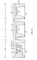
- FIG. 1is a process diagram showing a process of forming a thin oxide film and a thick oxide film that is a part of the manufacturing method of a semiconductor device according to a first embodiment of the present invention
- FIG. 2is a process diagram showing a process of forming a phosphorus-doped amorphous silicon film and a silicon nitride film that is a part of the manufacturing method of a semiconductor device according to the first embodiment of the present invention
- FIG. 3is a process diagram showing a process of forming a resist pattern that is a part of the manufacturing method of a semiconductor device according to the first embodiment of the present invention
- FIG. 4is a process diagram showing a process of forming a trench used for STI that is a part of the manufacturing method of a semiconductor device according to the first embodiment of the present invention
- FIG. 5is a process diagram showing a process of forming silicon oxide films that is a part of the manufacturing method of a semiconductor device according to the first embodiment of the present invention
- FIG. 6is a process diagram showing a process of forming element separation regions that is a part of the manufacturing method of a semiconductor device according to the first embodiment of the present invention
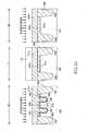
- FIG. 7is a process diagram showing a process of forming a resist pattern that is a part of the manufacturing method of a semiconductor device according to the first embodiment of the present invention.
- FIG. 8is a process diagram showing a process of patterning the silicon nitride film that is a part of the manufacturing method of a semiconductor device according to the first embodiment of the present invention.
- FIG. 9is a process diagram showing a process of forming gate trenches that is a part of the manufacturing method of a semiconductor device according to the first embodiment of the present invention.
- FIG. 10is a process diagram showing a process of forming a silicon oxide film that is a part of the manufacturing method of a semiconductor device according to the first embodiment of the present invention.
- FIG. 11is a process diagram showing a process of forming a phosphorus-doped amorphous silicon films into gate trenches that is a part of the manufacturing method of a semiconductor device according to the first embodiment of the present invention
- FIG. 12is a process diagram showing a process of etching-back the phosphorus-doped amorphous silicon films that is a part of the manufacturing method of a semiconductor device according to the first embodiment of the present invention
- FIG. 13is a process diagram showing a process of removing the silicon nitride film, the upper portions of the element separation regions, and the upper portions of the silicon oxide films that is a part of the manufacturing method of a semiconductor device according to the first embodiment of the present invention
- FIG. 14is a process diagram showing a process of forming a phosphorus-doped amorphous silicon film that is a part of the manufacturing method of a semiconductor device according to the first embodiment of the present invention
- FIG. 15is a process diagram showing a process of forming a resist pattern that is a part of the manufacturing method of a semiconductor device according to the first embodiment of the present invention.
- FIG. 16is a process diagram showing a process of patterning layered films that is a part of the manufacturing method of a semiconductor device according to the first embodiment of the present invention.
- FIG. 17is a process diagram showing a process of forming source/drain diffusion regions that is a part of the manufacturing method of a semiconductor device according to the first embodiment of the present invention.
- FIG. 18is a process diagram showing a process of forming various wiring patterns and cell capacitors that is a part of the manufacturing method of a semiconductor device according to the first preferred embodiment of the present invention.
- FIG. 19is a process diagram showing a process of forming a thin oxide film and a thick oxide film that is a part of the manufacturing method of a semiconductor device according to a second embodiment of the present invention.
- FIG. 20is a process diagram showing a process of forming a non-doped amorphous silicon film and a silicon nitride film that is a part of the manufacturing method of a semiconductor device according to the second embodiment of the present invention
- FIG. 21is a process diagram showing a process of forming a resist pattern that is a part of the manufacturing method of a semiconductor device according to the second embodiment of the present invention.
- FIG. 22is a process diagram showing a process of forming a trench used for STI that is a part of the manufacturing method of a semiconductor device according to the second embodiment of the present invention.
- FIG. 23is a process diagram showing a process of forming silicon oxide films that is a part of the manufacturing method of a semiconductor device according to the second embodiment of the present invention.
- FIG. 24is a process diagram showing a process of forming element separation regions that is a part of the manufacturing method of a semiconductor device according to the second embodiment of the present invention.
- FIG. 25is a process diagram showing a process of forming a resist pattern that is a part of the manufacturing, method of a semiconductor device according to the second embodiment of the present invention.
- FIG. 26is a process diagram showing a process of patterning the silicon nitride film that is a part of the manufacturing method of a semiconductor device according to the second embodiment of the present invention.
- FIG. 27is a process diagram showing a process of forming gate trenches that is a part of the manufacturing method of a semiconductor device according to the second embodiment of the present invention.
- FIG. 28is a process diagram showing a process of forming a silicon oxide film that is a part of the manufacturing method of a semiconductor device according to the second embodiment of the present invention.
- FIG. 29is a process diagram showing a process of forming a phosphorus-doped amorphous silicon films into gate trenches that is a part of the manufacturing method of a semiconductor device according to the second embodiment of the present invention.
- FIG. 30is a process diagram showing a process of etching-back the phosphorus-doped amorphous silicon films that is a part of the manufacturing method of a semiconductor device according to the second embodiment of the present invention.
- FIG. 31is a process diagram showing a process of removing the silicon nitride film, the upper portions of the element separation regions, and the upper portions of the silicon oxide films that is a part of the manufacturing method of a semiconductor device according to the second embodiment of the present invention
- FIG. 32is a process diagram showing a process of forming a non-doped amorphous silicon film that is a part of the manufacturing method of a semiconductor device according to the second embodiment of the present invention.
- FIG. 33is a process diagram showing a process of implanting boron ion that is a part of the manufacturing method of a semiconductor device according to the second embodiment of the present invention.
- FIG. 34is a process diagram showing a process of implanting phosphorus ion that is a part of the manufacturing method of a semiconductor device according to the second embodiment of the present invention.
- FIG. 35is a process diagram showing a process of forming resist patterns that is a part of the manufacturing method of a semiconductor device according to the second embodiment of the present invention.
- FIG. 36is a process diagram showing a process of patterning layered films that is a part of the manufacturing method of a semiconductor device according to the second embodiment of the present invention.
- FIG. 37is a process diagram showing a process of forming source/drain diffusion regions that is a part of the manufacturing method of a semiconductor device according to the second embodiment of the present invention.
- FIG. 38is a process diagram showing a process of forming various wiring patterns and cell capacitors that is a part of the manufacturing method of a semiconductor device according to the second embodiment of the present invention.
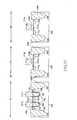
- FIG. 39is a process diagram showing a process of forming an STI and a gate trenchthat is a part of a conventional method
- FIG. 40is a process diagram showing a process of forming a silicon oxide film that is a part of the conventional method
- FIG. 41is a process diagram showing a process of removing a resist pattern and the silicon oxide film formed on the region PE that is a part of the conventional method;
- FIG. 42is a process diagram showing a process of forming a thin oxide film and a thick oxide film that is a part of the conventional method
- FIG. 43is a process diagram showing a process of forming a doped silicon film that is a part of the conventional method.
- FIG. 44is a process diagram showing a process of patterning the doped silicon film that is a part of the conventional method.
- FIGS. 1 through 18are schematic views showing the process for manufacturing a semiconductor device that has a trench-gate transistor and a planar transistor according to a first embodiment of the present invention.
- region Mindicates the memory cell region in which the trench-gate transistor is formed
- region PEindicates the peripheral circuit region in which the planar transistor is formed.
- a thin oxide film 11 s having a thickness of approximately 1.5 to 3 nmis formed on the surface of region PE of a semiconductor substrate 10 , as shown in FIG. 1 .
- a thick oxide film 11 t having a thickness of approximately 4.5 to 6 nmis also formed in region M and in a region (not shown) in which a power supply circuit and the like are formed, and which is a region other than region PE of the peripheral circuit region.
- a thermal oxide film having a thickness of slightly less than 6 nmis formed on the entire surface of the semiconductor substrate 10 by thermal oxidation, the region other than region PE is covered by a resist mask, and the thermal oxide film on region PE is removed, after which the resist mask is removed, and the entire surface of the substrate 10 is cleaned with an acid.
- This cleaningremoves a portion of the surface of the thermal oxide film on region M and on the region (not shown) in which a power supply circuit and the like are formed, and the thickness of the thermal oxide film is reduced to about 5 nm.
- the entire surfaceis again thermal-oxidized to form a thin oxide film 11 s having a thickness of about 3 nm on region PE, and a thick oxide film lit having a thickness of about 6 nm on region M and the region (not shown) in which a power supply circuit and the like are formed.
- the thin oxide film 11 s thereby formedis the gate insulating film of the planar transistor formed in region PE.
- the thickness of the oxide film lit formed in region M hereinmay be equal to that of the thin oxide film 11 s.
- the oxide film lit in region Mis preferably formed thick as described above so that in a case in which the gate electrode of the trench-gate transistor formed in region M is formed in a shape that protrudes further than the surface of the semiconductor substrate 10 , even when the protruding portion is misaligned with respect to the gate trench 18 , high breakdown voltage can be maintained in the misaligned portion as well.
- the thick oxide film 11 tis also the gate insulating film of a transistor having a high breakdown voltage that is formed in a region (not shown) in which a power supply circuit and other components are formed.
- a phosphorus-doped amorphous silicon film 12 as a protective film that has a thickness of approximately 10 to 30 nmis then formed by a CVD (Chemical Vapor Deposition) method in order to protect the thin oxide film 11 s.
- a silicon nitride film 13 having a thickness of approximately 80 to 150 nmis then formed by an LP (Low Pressure)-CVD method.
- a resist pattern 14is formed on each element separation region formed as a region for separating elements according to the STI (Shallow Trench Isolation) technique.
- the phosphorus-doped amorphous silicon films 12 , the thick oxide films 11 t, the thin oxide films 11 s, and the semiconductor substrate 10are dry-etched using the patterned silicon nitride films 13 as masks.
- the phosphorus-doped amorphous silicon films 12 , the thick oxide films 11 t, and the thin oxide films 11 sare thereby patterned, and trenches 15 used for STI are also formed in the semiconductor substrate 10 .
- a thermal oxidation treatmentis then performed in order to remove the etching damage from the inner walls of the trenches 15 , after which silicon oxide films 16 are formed on the entire surface by an HDP (High-Density Plasma)-CVD method so as to fill in the trenches 15 , as shown in FIG. 5 .
- HDPHigh-Density Plasma
- CMPChemical Mechanical Polishing
- a resist pattern 17 that is provided with a plurality of openingsis then formed on region M in order to form the gate trenches of the trench-gate memory cell transistor in region M.
- Region PEis completely covered at this time by resist patterns 17 . Openings are also formed in the resist pattern 17 above the element separation regions 16 i of region M in order to be used for a gate trench that is formed in an adjacent memory cell region (not shown).
- the silicon nitride film 13is then patterned in the shape of the mask, as shown in FIG. 8 .
- the phosphorus-doped amorphous silicon film 12 and the thick oxide film 11 tare etched, and the semiconductor substrate 10 is also etched, whereby gate trenches 18 are formed in the semiconductor substrate 10 , as shown in FIG. 9 .
- the silicon nitride film 13 that was used as a mask for forming the STI trenches 15 shown in FIG. 4thus remains without being removed, and is also used as a mask for forming the gate trenches 18 , as shown in FIG. 9 .
- a silicon oxide film 19is then formed to act as the gate insulating film of the memory cell transistor, as shown in FIG. 10 .
- This silicon oxide film 19must also have high voltage resistance as described above, and preferably has a thickness of approximately 4.5 to 6 nm.
- the silicon oxide film 19 hereinis preferably formed by a process in which a CVD oxide film (preferably a HTO (High Temperature Oxide)) having a thickness of approximately 3.5 to 5.5 nm is deposited by a CVD method at a temperature of approximately 800° C., after which the CVD oxide film is thermally oxidized at a temperature of approximately 1050° C. in order to densify the CVD oxide film, remove impurities, and modify the interface between the CVD oxide film and the semiconductor substrate 10 .
- the time needed to form the second gate insulating film in the gate trenchcan thereby be prevented from increasing even when further reduction in size narrows the opening of the gate trench, and an increase in oxidation stress can also be suppressed.
- the silicon oxide film 19is preferably formed according to the method described above.
- the thin oxide film 11 s formed on the semiconductor substrate 10 in region PEis covered by the phosphorus-doped amorphous silicon film 12 that is the protective film, it is possible to prevent a CVD oxide film from being deposited on the thin oxide film 11 s, and to prevent the thin oxide film 11 s from becoming thicker as a result of thermal oxidation.
- an amorphous silicon film that is doped with phosphorus as an N-type impurityis then formed on the entire surface that includes the insides of the gate trenches 18 .
- Phosphorus-doped amorphous silicon films 20are then embedded in the gate trenches 18 as shown in FIG. 11 , by performing a planarization process according to a CMP method in which the silicon nitride film 13 is used as a stopper.
- the phosphorus-doped amorphous silicon films 20 in the gate trenches 18are then etched back to about the same position as the thick oxide film 11 t by dry etching, as shown in FIG. 12 .
- wet etchingis then performed to remove the silicon nitride film 13 , the upper portions of the element separation regions 16 i, and the upper portions of the silicon oxide films 19 .
- the upper surfaces of the element separation regions 16 i and the phosphorus-doped amorphous silicon film 12are thereby aligned with each other, as shown in FIG. 13 .
- the phosphorus-doped amorphous silicon film 12is formed on the gate insulating film 11 s in region PE, and is made to function as a protective film when the nitride film 13 (see FIG. 12 ) used as a mask for forming the gate trench 18 is removed. It is therefore possible to prevent the gate insulating film 11 s from being damaged.
- a CVD methodis then used to form an amorphous silicon film (phosphorus-doped amorphous silicon film) 21 that is doped with phosphorus as an N-type impurity and has a thickness of approximately 30 to 80 nm on the entire surface, as shown in FIG. 14 .
- a resist pattern 22 used to form a gate electrodeis then formed on the phosphorus-doped amorphous silicon film 21 , as shown in FIG. 15 .
- the phosphorus-doped amorphous silicon film 21is then patterned using a resist pattern 22 as a mask, as shown in FIG. 16 .
- a gate electrode of a trench-gate transistor composed of the phosphorus-doped amorphous silicon films 20 and 21is thereby formed in region M, and a gate electrode of a planar transistor composed of the phosphorus-doped amorphous silicon films 12 and 21 is formed in region PE.
- the example described hereinis of a case in which the patterned amorphous silicon films 21 are not misaligned with respect to the gate trenches 18 in region M. However, when misalignment does occur, the amorphous silicon films 21 remain on the thick oxide film lit and become portions of a gate electrode. In this type of case, the thick oxide film 11 t functions as a portion of the gate insulating film in this trench-gate transistor. However, since the oxide film t is formed so as to have about the same thickness as the silicon oxide films 19 in the gate trenches 18 , a reduction in the breakdown voltage thereof can be minimized.
- N-type source/drain diffusion regions 23are formed in region M, and N-type source/drain diffusion regions 24 are formed in region PE by ion implantation of an N-type impurity into regions M and PE using each gate electrode as a mask, as shown in FIG. 17 .
- a trench-gate memory cell transistoris thereby formed in region M, and a planar transistor is formed in region PE.
- the amorphous silicon films 12 , 20 and 21are converted from amorphous silicon films to polycrystalline silicon films by the heat treatment performed to activate the source/drain diffusion regions, or by a subsequent heating process.
- DRAM having a trench-gate memory cell transistoris formed by a process in which an interlayer insulating film 25 is formed on the memory cell transistor, and a contact plug 26 that pass through the interlayer insulating film 25 , a bit line 27 , a cell capacitor 28 , Al wiring 29 , and other components are formed, as shown in FIG. 18 .
- a thin oxide film 11 sis formed in advance to function as the gate insulating film of the planar transistor on the semiconductor substrate 10 of the peripheral circuit region PE, and this thin oxide film 11 s is covered by the amorphous silicon film 12 .
- a gate trench 18is formed in memory cell region M, and a gate insulating film 19 that is thicker than the gate insulating film 11 s is formed on the inner wall of the gate trench 18 . Since the amorphous silicon film 12 thereby functions as a protective film for preventing growth of the gate insulating film 11 s, the gate insulating film 19 can be made thick while the gate insulating film 11 s remains thin. Specifically, the gate insulating film 11 s and the gate insulating film 19 can be formed independently of each other. The number of oxidation steps performed in the gate trench 18 can therefore be reduced.
- oxidation stress in the gate trench 18can be reduced, and a degradation of the refresh characteristics can be prevented. Since the gate insulating film 11 s and the gate insulating film 19 are formed independently rather than simultaneously, the film thickness and other characteristics are easily controlled.
- a dual-gate-structured transistor having a thin oxide film as the gate insulating filmis formed in the peripheral circuit region.
- a gate electrode that includes N-type polycrystalline silicon into which an N-type impurity (phosphorus or the like) is introducedis used as the gate electrode of an N-channel transistor
- a gate electrode that includes P-type polycrystalline silicon into which a P-type impurity (boron or the like) is introducedis used in a P-channel transistor.
- FIGS. 19 through 38are schematic views showing the process for manufacturing a semiconductor device that has a trench-gate transistor and a dual-gate-structured transistor according to a second embodiment of the present invention.
- region Mindicates the memory cell region in which the trench-gate transistor is formed
- region Pand “region N” are provided to the peripheral circuit region
- region Pis a region (also referred to as a P-type peripheral circuit region) in which a planar P-channel transistor provided with a gate electrode that includes P-type polycrystalline silicon is formed
- region Nis a region (also referred to as an N-type peripheral circuit region) in which a planar N-channel transistor provided with a gate electrode that includes N-type polycrystalline silicon is formed.
- a thin oxide film 101 s having a thickness of approximately 1.5 to 3 nmis formed on the surface of regions P and N of a semiconductor substrate 100 , as shown in FIG. 19 .
- a thick oxide film 101 t having a thickness of approximately 4.5 to 6 nmis also formed in region M and in a region (not shown) in which a power supply circuit and the like are formed, and which is a region other than region P or N of the peripheral circuit region.
- the thin oxide film 101 s and the thick oxide film 101 tare formed in the same manner as the thin oxide film 11 s and the thick oxide film t in the process shown in FIG. 1 in the abovementioned first embodiment.
- the thin oxide film 101 s thus formedis the gate insulating film of a dual-gate-structured planar transistor formed in regions P and N.
- the thickness of the oxide film 101 t formed in region Mmay be the same as that of the thin oxide film 101 s, but a thick film is preferred for the same reason as in the first embodiment.
- the thick oxide film 101 tis the gate insulating film of a transistor having a high breakdown voltage that is formed in a region (not shown) in which a power supply circuit and other components are formed, the same as the thick oxide film 11 t in the first embodiment.
- a non-doped amorphous silicon film 102 as a protective film that has a thickness of approximately 10 to 30 nmis then formed by a CVD (Chemical Vapor Deposition) method in order to protect the thin oxide film 101 s.
- CVDChemical Vapor Deposition
- a non-doped amorphous silicon filmis used as the protective film instead of the doped amorphous silicon film used in the abovementioned first embodiment.
- a silicon nitride film 103 having a thickness of approximately 80 to 150 nmis then formed by an LP (Low Pressure)-CVD method.
- a resist pattern 104is formed on each element separation region formed as a region for separating elements according to the STI (Shallow Trench Isolation) technique.
- the non-doped amorphous silicon films 102 , the thick oxide films 101 t, the thin oxide films 101 s, and the semiconductor substrate 100are dry-etched using the patterned silicon nitride films 103 as masks.
- the non-doped amorphous silicon films 102 , the thick oxide films 101 t, and the thin oxide films 101 sare thereby patterned, and trenches 105 used for STI are also formed in the semiconductor substrate 100 .
- a thermal oxidation treatmentis then performed in order to remove the etching damage from the inner walls of the trenches 105 , after which silicon oxide films 106 are formed on the entire surface by an HDP (High-Density Plasma)-CVD method so as to fill in the trenches 105 , as shown in FIG. 23 .
- HDPHigh-Density Plasma
- CMPChemical Mechanical Polishing
- a resist pattern 107 that is provided with a plurality of openingsis then formed on region M in order to form the gate trenches of the trench-gate memory cell transistor in region M. Regions P and N are completely covered at this time by resist patterns 107 .
- the silicon nitride film 103is then patterned in the shape of the mask, as shown in FIG. 26 .
- the non-doped amorphous silicon film 102 and the thick oxide film 101 tare etched, and the semiconductor substrate 100 is also etched, whereby gate trenches 108 are formed in the semiconductor substrate 100 , as shown in FIG. 27 .
- the silicon nitride film 103 that was used as a mask for forming the STI trenches 105 shown in FIG. 22thus remains without being removed, and is also used as a mask for forming the gate trenches 108 , as shown in FIG. 27 .
- a silicon oxide film 109is then formed to act as the gate insulating film of the memory cell transistor, as shown in FIG. 28 .
- This silicon oxide film 109is the gate insulating film of the memory cell transistor, and therefore must have a high breakdown voltage, as in the first embodiment, and the thickness thereof is preferably about B 4 . 5 to 6 nm.
- This silicon oxide film 109can be formed in the same manner as the silicon oxide film 19 formed in the steps of the first embodiment shown in FIG. 10 .
- the thin oxide film 101 s formed on the semiconductor substrate 100 of regions P and Nis covered at this time by a non-doped amorphous silicon film 102 , which is a protective film. It is therefore possible to prevent an oxide film from being further deposited on the thin oxide film 101 s, and to prevent the thin oxide film 101 s from increasing in thickness due to thermal oxidation.
- an amorphous silicon film that is doped with phosphorus as an N-type impurityis then formed on the entire surface that includes the insides of the gate trenches 108 .
- Phosphorus-doped amorphous silicon films 110are then embedded in the gate trenches 108 as shown in FIG. 29 , by performing a planarization process according to a CMP method in which the silicon nitride film 103 is used as a stopper.
- the phosphorus-doped amorphous silicon films 110 in the gate trenches 108are then etched back to about the same position as the thick oxide film 101 t by dry etching, as shown in FIG. 30 .
- wet etchingis then performed to remove the silicon nitride film 103 , the upper portions of the element separation regions 106 i, and the upper portions of the silicon oxide films 109 .
- the upper surfaces of the element separation regions 106 i and the protective film (non-doped amorphous silicon film) 102are thereby aligned with each other, as shown in FIG. 31 .
- a CVD methodis then used to form a non-doped amorphous silicon film 111 having a thickness of approximately 30 to 80 nm to become the gate electrode of the dual-gate transistor, as shown in FIG. 32 .
- a dual-gate-structured transistoris formed in regions P and N in the present embodiment.
- a non-doped amorphous silicon filmis therefore used instead of a doped amorphous silicon film as the film for forming the gate electrode.
- regions M and Nare then masked by a resist pattern 112 , and boron (B) as a P-type impurity is ion-implanted into region P.
- This ion implantation of boronis performed at a low energy of 10 keV or less.
- the implanted boron ionsare diffused in a subsequently performed heat treatment, whereby the non-doped amorphous silicon films 111 and 102 (see FIG. 32 ) of region P become P-type amorphous silicon films 111 p and 102 p.
- region P in this instanceis masked by a resist pattern 113 , and phosphorus (P) as an N-type impurity is ion-implanted into regions M and N, as shown in FIG. 34 .
- This ion implantation of phosphorusis also performed at a low energy of 20 keV or less, the same as the ion implantation of boron described above, and the phosphorus ions are diffused by a subsequent heat treatment.
- the non-doped amorphous silicon films 111 and 102 (see FIG. 33 ) of region Nthereby become N-type amorphous silicon films 111 n and 102 n.
- the non-doped amorphous silicon films 111 and 102 of region Mare also made into N-type amorphous silicon films 111 n and 102 n by this ion implantation.
- phosphorus-doped silicon films 110are already embedded in the gate trenches 108 of region M. Ion implantation can therefore be performed under suitable implantation conditions according to the thickness of the silicon film 111 and the silicon film 102 without regard to implantation into the gate trenches 108 when ion implantation into region M is performed at the same time as phosphorus is implanted into region N in the ion implantation process for creating P-type and N-type non-doped silicon films 111 , which are the gate electrodes of the dual-gate transistor.
- Resist patterns 114 for use in forming gate electrodesare then formed on the impurity-doped amorphous silicon films 111 n and 111 p, as shown in FIG. 35 .
- the layered film that includes the amorphous silicon films 111 p and 102 p, as well as the layered film that includes the amorphous silicon films 111 n and 102 n,are then each patterned using the resist pattern 114 as a mask.
- a gate electrode of a trench-gate transistor composed of doped amorphous silicon films 110 and 111 nis thereby formed in region M
- a P-type gate electrode composed of doped amorphous silicon films 111 p and 102 pis formed in region P
- an N-type gate electrode composed of doped amorphous silicon films 111 n and 102 nis formed in region N.
- regions M and Nare then covered by a resist film (not shown), and P-type source/drain diffusion regions 115 p are formed by ion-implanting a P-type impurity into region P using the P-type gate electrode as a mask.
- Region Pis then covered by a resist film (not shown), and an N-type impurity is ion-implanted into regions M and N using the gate electrodes of regions M and N as masks.
- N-type source/drain diffusion regions 115 nare thereby formed in region N, and N-type source/drain diffusion regions 116 are formed in region M.
- a trench-gate memory cell transistoris formed in region M, and a dual-gate transistor is formed in regions P and N, which are peripheral circuit regions.
- the amorphous silicon films 111 n, 111 p, 102 p, 102 n, and 110are converted from amorphous silicon films to polycrystalline silicon films by the heat treatment performed to activate the source/drain diffusion regions, or by a subsequent heating process.
- DRAM having a trench-gate memory cell transistoris formed by a process in which an interlayer insulating film 117 is formed on the memory cell transistor, and a contact plug 118 that pass through the interlayer insulating film 117 , a bit line 119 , a cell capacitor 120 , Al wiring 121 , and other components are formed, as shown in FIG. 38 .
- a thin oxide film 101 sis formed in advance on the semiconductor substrate 100 of regions P and N in the peripheral circuit region to become the gate insulating film of the dual-gate-structured transistor that is formed in regions P and N.
- a gate trench 108is then formed in the memory cell region M in a state in which the thin oxide film 101 s is covered by an amorphous silicon film 102 , and a gate insulating film 109 that is thicker than the gate insulating film 101 s is formed on the inner wall of the gate trench 108 , whereby the gate insulating film 101 s and the gate insulating film 109 can be formed independently of each other.
- an amorphous silicon film 110 that is selectively doped with an impuritycan be formed in the gate trench 108 of region M.
- the following processesare involved in an example of a possible method for selectively forming doped silicon in the gate trench when a trench-gate transistor and a dual-gate-structured transistor are formed on the same substrate.
- a thermal oxide film serving as the gate insulating film of the transistorsis formed in the gate trench and on the semiconductor substrate in the peripheral circuit region in which the dual-gate-structured transistor is formed, and a doped silicon film is formed on the entire surface that includes the inside of the gate trench.
- the doped silicon filmis then etched back so as to remain only in the gate trench, a non-doped silicon film is formed on the gate insulating film to be used for the gate electrode of the dual-gate-structured transistor, and P- and N-type gate electrodes are each formed by ion implantation.
- the gate insulating film of the dual-gate-structured transistoris usually damaged when the doped silicon is etched back, making it difficult to form a high-performance transistor.
- a non-doped amorphous silicon film 102is formed on the gate insulating film 101 s on regions P and N, which are the regions in which the dual-gate-structured transistor is formed, in the step for removing the silicon nitride film 103 that is used as a mask for forming the gate trench 108 , the gate insulating film 109 , the doped silicon film 110 that is embedded in the gate trench 108 , and the gate trench 108 . Damage to the gate insulating film 101 s can thereby be prevented when the mask nitride film 103 is removed.
- an impurity-doped amorphous silicon film 110 in the gate trench 108it is possible to form an impurity-doped amorphous silicon film 110 in the gate trench 108 , and to form a non-doped amorphous silicon film 111 on regions P and N as well as on the doped amorphous silicon film 110 that was embedded in the gate trenches.
- the silicon films 110 , 111 , and 102can thereby be formed in the appropriate impurity concentrations without damaging the gate insulating film 101 s, and the trench-gate transistor and the dual-gate-structured transistor can both be endowed with high performance.
- an amorphous silicon film 110 that is selectively doped with an impuritycan be formed in the gate trench 108 . Depletion of the trench-gate electrode can thereby be prevented in contrast to a case in which an impurity is introduced after a non-doped silicon film is formed in the gate trench.
- the protective film used for covering the thin oxide film 11 s ( 101 s )was a doped amorphous silicon film 12 in the first embodiment, and a non-doped amorphous silicon film 102 in the second embodiment.
- these configurationsare not limiting, and another material may also be used insofar as the resulting film can prevent an oxide film from being layered on the thin oxide film 11 s ( 101 s ) when the gate insulating film 19 ( 109 ) is formed in the gate trench 18 ( 108 ), or thickness from being increased due to further oxidation, while the operation of the transistors is not impeded.
- another materialmay be used insofar as the resulting film (conductive thin film or the like) allows formation of a channel needed during the application of voltage to a gate electrode.
- each silicon filmwas first formed in an amorphous state and then converted to a polycrystalline silicon film by a subsequent heating process.
- polycrystalline silicon filmsmay also be used initially as needed.
- a layered film that included silicon films 12 ( 102 ) and 21 ( 111 )was used as the gate electrode of the planar transistor, but the silicon film 12 ( 102 ), which is a protective film, may be formed in advance so as to initially have the required thickness as a gate electrode in cases in which the gate trench 108 or the STI trench 15 ( 105 ) has a small depth, and in other cases.
- the gate electrodeis also not necessarily formed using only silicon films, and it is also possible to form a silicide layer on a silicon film, or to create a so-called polymetal gate electrode by layering metal films.
- the example described abovewas one in which the mask layer for forming the trenches 15 ( 105 ) that were used for STI, and the mask layer for forming the gate trenches 18 ( 108 ) were used in common in the silicon nitride film 13 ( 103 ).
- the silicon nitride film 13 ( 103 )may be removed after the STI (element separation regions) 16 i ( 106 i ) are formed, and a new silicon nitride film may be created to form a mask layer.
Landscapes
- Engineering & Computer Science (AREA)
- Manufacturing & Machinery (AREA)
- Semiconductor Memories (AREA)
- Metal-Oxide And Bipolar Metal-Oxide Semiconductor Integrated Circuits (AREA)
- Electrodes Of Semiconductors (AREA)
- Element Separation (AREA)
- Non-Volatile Memory (AREA)
Abstract
Description
- The present invention relates to method for manufacturing a semiconductor device, and particularly relates to a method for manufacturing a semiconductor device having both a trench-gate transistor and a planar transistor.
- The recent miniaturization of DRAM (Dynamic Random Access Memory) cells has been accompanied by the necessity of shortening the gate length of memory cell transistors. However, short channel effects in a transistor become more severe as the gate length is shortened, and drawbacks occur whereby sub-threshold current increases. When the substrate impurity concentration is increased in order to minimize this effect, deterioration of the refresh characteristics in the DRAM is a severe drawback because of increased junction leakage.
- A so-called trench-gate transistor (also referred to as a recess-channel transistor) in which a gate electrode is embedded in a groove formed on a silicon substrate has been emphasized as a means of overcoming these drawbacks (see Japanese Laid-open Patent Application Nos. H9-232535, 2001-210801, 2005-142203, H7-066297, and 2004-014696). Using a trench-gate transistor, the effective channel length (gate length) can be physically and adequately maintained, and it is possible to create precision DRAM having a minimum feature size of 90 nm or less.
- On the other hand, in DRAM, since there is little need to make the gate length of the transistors in the peripheral circuit region compared with the transistor in the memory cell region, a normal planar transistor is formed in the peripheral circuit region.
- Accordingly, trench-gate transistors and planar transistors should be simultaneously formed on a single semiconductor substrate.
- However, the thickness of the gate oxide film must be reduced for the sake of low-voltage operation in most of the transistors formed in the peripheral circuit region, whereas a boost voltage is applied to the transistors formed in the memory cell region, and a high breakdown voltage is therefore required. Specifically, a thick gate insulating film is required in the memory cell region.
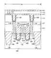
FIGS. 39 through 44 are used hereinafter to describe a conventional method for providing the memory cell region with a trench-gate transistor in which the gate insulating film is a thick oxide film, and providing the peripheral circuit region with a planar transistor in which the gate insulating film is a thin oxide film. InFIGS. 39 through 44 , “region M” indicates the memory cell region, and “region PE” indicates the region provided with a planar transistor that uses a thin oxide film as the gate insulating film in the peripheral circuit region. The peripheral circuit region also includes a region (not shown) in which a power supply circuit and the like are formed, and which is a region other than region PE.- As shown in
FIG. 39 , agate trench 202 is formed in region M of asemiconductor substrate 200 whose regions are separated by STI (Shallow Trench Isolation)201. Although not shown in the drawing, sacrificial oxidation is then performed by thermal oxidation to remove damage and contamination from the etched surfaces inside thegate trench 202, after which a somewhat thicksilicon oxide film 203 is formed by thermal oxidation on the entire surface that includes the inner wall of thegate trench 202, as shown inFIG. 40 . As shown inFIG. 41 , region M is then covered, aresist pattern 204 for exposing region PE is formed, and thesilicon oxide film 203 in region PE is removed by wet etching using theresist pattern 204 as a mask. Then, after theresist pattern 204 is removed, the entire surface is again oxidized by thermal oxidation. Thesilicon oxide film 203 on the surface of thesubstrate 200 and the inner wall of thegate trench 202 in region M thereby grows thicker, as shown inFIG. 42 , yielding athick oxide film 205tthat serves as the gate insulating film of the trench-gate transistor. At the same time, athin oxide film 205sis formed in region PE to be the gate insulating film of the planar transistor. - A doped
silicon film 206 is then formed on the entire surface so as to fill in thegate trench 202, as shown inFIG. 43 , and thedoped silicon film 206 is patterned in the shape of a gate electrode. Thegate electrode 208 of the trench-gate transistor and thegate electrode 207 of the planar transistor are thereby formed, as shown inFIG. 44 . Ion implantation is then performed for eachsemiconductor substrate 200 using thegate electrodes drain diffusion regions 209 are formed in region PE, and source/drain diffusion regions 210 are formed in region M. A planar transistor having a thick gate insulating film is thereby formed in region PE, and a trench-gate transistor having a thin gate insulating film is formed in region M. - However, the conventional method described above has the following types of drawbacks.
- Specifically, the method described above requires at least three thermal oxidation steps to be performed in the
gate trench 202 that include sacrificial oxidation, thermal oxidation for forming thesilicon oxide film 203, and thermal oxidation for causing thesilicon oxide film 203 to grow into thethick oxide film 205t.Oxidation stress inside thegate trench 202 thereby increases, and the DRAM refresh characteristics are adversely affected. - Since the opening of the
gate trench 202 becomes narrow as the size of the device is reduced, the oxidation rate inside thegate trench 202 decreases, and the oxidation rate inside thegate trench 202 therefore becomes lower than that of the flat portion (surface of the substrate200). Therefore, when an attempt is made to form an oxide film in region PE at the same time as an oxide film having the necessary thickness is formed inside thegate trench 202, the oxide film on the surface of region PE becomes too thick. Thesilicon oxide film 203 on region PE must then be temporarily removed, as shown inFIG. 41 . - The present invention was developed in order to overcome the drawbacks described above, and an object of the present invention is to provide a method for manufacturing a semiconductor device whereby the process is simplified and both transistors can be endowed with high performance in a case in which a trench-gate transistor having a thick gate insulating film, and a planar transistor having a thin gate insulating film are both formed on the same semiconductor substrate.
- The above and other objects of the present invention can be accomplished by a method for manufacturing a semiconductor device that has a memory cell region and a peripheral circuit region, said method comprising:
- a first step for forming a first gate insulating film on a semiconductor substrate in at least said peripheral circuit region;
- a second step for covering said first gate insulating film with a protective film;
- a third step for forming a gate trench in said memory cell region in a state in which said first gate insulating film on said peripheral circuit region is covered by said protective film; and
- a fourth step for forming a second gate insulating film that is thicker than said first gate insulating film on at least an inner wall of said gate trench in a state in which said first gate insulating film on said peripheral circuit region is covered by said protective film.
- According to the present invention, a gate trench is formed in the memory cell region, and then a second gate insulating film that is thicker than the first gate insulating film is formed on the inner wall of the gate trench in a state in which the first gate insulating film on the peripheral circuit region is covered by a protective film. The first gate insulating film and the second gate insulating film can therefore be formed independently of each other. Accordingly, the number of oxidation steps performed in the gate trench can be reduced. Oxidation stress in the gate trench can thereby be reduced, and a degradation of the refresh characteristics can be prevented. Since the first gate insulating film and the second gate insulating film are formed independently rather than simultaneously, the film thickness and other characteristics are easily controlled. It is also possible to provide a method for manufacturing a semiconductor device whereby the process is simplified, and both transistors can be endowed with high performance in a case in which a trench-gate transistor having a thick gate insulating film, and a planar transistor having a thin gate insulating film are both formed on the same semiconductor substrate.
- The abovementioned second gate insulating film in particular is preferably formed by a step for depositing a silicon oxide film by a CVD method, and by a step for thermal-oxidizing the interface between the silicon oxide film and the semiconductor substrate. The time needed to form the second gate insulating film in the gate trench can thereby be prevented from increasing even when further reduction in size narrows the opening of the gate trench, and an increase in oxidation stress can be suppressed.
- The above and other objects, features and advantages of this invention will become more apparent by reference to the following detailed description of the invention taken in conjunction with the accompanying drawings, wherein:
FIG. 1 is a process diagram showing a process of forming a thin oxide film and a thick oxide film that is a part of the manufacturing method of a semiconductor device according to a first embodiment of the present invention;FIG. 2 is a process diagram showing a process of forming a phosphorus-doped amorphous silicon film and a silicon nitride film that is a part of the manufacturing method of a semiconductor device according to the first embodiment of the present invention;FIG. 3 is a process diagram showing a process of forming a resist pattern that is a part of the manufacturing method of a semiconductor device according to the first embodiment of the present invention;FIG. 4 is a process diagram showing a process of forming a trench used for STI that is a part of the manufacturing method of a semiconductor device according to the first embodiment of the present invention;FIG. 5 is a process diagram showing a process of forming silicon oxide films that is a part of the manufacturing method of a semiconductor device according to the first embodiment of the present invention;FIG. 6 is a process diagram showing a process of forming element separation regions that is a part of the manufacturing method of a semiconductor device according to the first embodiment of the present invention;FIG. 7 is a process diagram showing a process of forming a resist pattern that is a part of the manufacturing method of a semiconductor device according to the first embodiment of the present invention;FIG. 8 is a process diagram showing a process of patterning the silicon nitride film that is a part of the manufacturing method of a semiconductor device according to the first embodiment of the present invention;FIG. 9 is a process diagram showing a process of forming gate trenches that is a part of the manufacturing method of a semiconductor device according to the first embodiment of the present invention;FIG. 10 is a process diagram showing a process of forming a silicon oxide film that is a part of the manufacturing method of a semiconductor device according to the first embodiment of the present invention;FIG. 11 is a process diagram showing a process of forming a phosphorus-doped amorphous silicon films into gate trenches that is a part of the manufacturing method of a semiconductor device according to the first embodiment of the present invention;FIG. 12 is a process diagram showing a process of etching-back the phosphorus-doped amorphous silicon films that is a part of the manufacturing method of a semiconductor device according to the first embodiment of the present invention;FIG. 13 is a process diagram showing a process of removing the silicon nitride film, the upper portions of the element separation regions, and the upper portions of the silicon oxide films that is a part of the manufacturing method of a semiconductor device according to the first embodiment of the present invention;FIG. 14 is a process diagram showing a process of forming a phosphorus-doped amorphous silicon film that is a part of the manufacturing method of a semiconductor device according to the first embodiment of the present invention;FIG. 15 is a process diagram showing a process of forming a resist pattern that is a part of the manufacturing method of a semiconductor device according to the first embodiment of the present invention;FIG. 16 is a process diagram showing a process of patterning layered films that is a part of the manufacturing method of a semiconductor device according to the first embodiment of the present invention;FIG. 17 is a process diagram showing a process of forming source/drain diffusion regions that is a part of the manufacturing method of a semiconductor device according to the first embodiment of the present invention;FIG. 18 is a process diagram showing a process of forming various wiring patterns and cell capacitors that is a part of the manufacturing method of a semiconductor device according to the first preferred embodiment of the present invention;FIG. 19 is a process diagram showing a process of forming a thin oxide film and a thick oxide film that is a part of the manufacturing method of a semiconductor device according to a second embodiment of the present invention;FIG. 20 is a process diagram showing a process of forming a non-doped amorphous silicon film and a silicon nitride film that is a part of the manufacturing method of a semiconductor device according to the second embodiment of the present invention;FIG. 21 is a process diagram showing a process of forming a resist pattern that is a part of the manufacturing method of a semiconductor device according to the second embodiment of the present invention;FIG. 22 is a process diagram showing a process of forming a trench used for STI that is a part of the manufacturing method of a semiconductor device according to the second embodiment of the present invention;FIG. 23 is a process diagram showing a process of forming silicon oxide films that is a part of the manufacturing method of a semiconductor device according to the second embodiment of the present invention;FIG. 24 is a process diagram showing a process of forming element separation regions that is a part of the manufacturing method of a semiconductor device according to the second embodiment of the present invention;FIG. 25 is a process diagram showing a process of forming a resist pattern that is a part of the manufacturing, method of a semiconductor device according to the second embodiment of the present invention;FIG. 26 is a process diagram showing a process of patterning the silicon nitride film that is a part of the manufacturing method of a semiconductor device according to the second embodiment of the present invention;FIG. 27 is a process diagram showing a process of forming gate trenches that is a part of the manufacturing method of a semiconductor device according to the second embodiment of the present invention;FIG. 28 is a process diagram showing a process of forming a silicon oxide film that is a part of the manufacturing method of a semiconductor device according to the second embodiment of the present invention;FIG. 29 is a process diagram showing a process of forming a phosphorus-doped amorphous silicon films into gate trenches that is a part of the manufacturing method of a semiconductor device according to the second embodiment of the present invention;FIG. 30 is a process diagram showing a process of etching-back the phosphorus-doped amorphous silicon films that is a part of the manufacturing method of a semiconductor device according to the second embodiment of the present invention;FIG. 31 is a process diagram showing a process of removing the silicon nitride film, the upper portions of the element separation regions, and the upper portions of the silicon oxide films that is a part of the manufacturing method of a semiconductor device according to the second embodiment of the present invention;FIG. 32 is a process diagram showing a process of forming a non-doped amorphous silicon film that is a part of the manufacturing method of a semiconductor device according to the second embodiment of the present invention;FIG. 33 is a process diagram showing a process of implanting boron ion that is a part of the manufacturing method of a semiconductor device according to the second embodiment of the present invention;FIG. 34 is a process diagram showing a process of implanting phosphorus ion that is a part of the manufacturing method of a semiconductor device according to the second embodiment of the present invention;FIG. 35 is a process diagram showing a process of forming resist patterns that is a part of the manufacturing method of a semiconductor device according to the second embodiment of the present invention;FIG. 36 is a process diagram showing a process of patterning layered films that is a part of the manufacturing method of a semiconductor device according to the second embodiment of the present invention;FIG. 37 is a process diagram showing a process of forming source/drain diffusion regions that is a part of the manufacturing method of a semiconductor device according to the second embodiment of the present invention;FIG. 38 is a process diagram showing a process of forming various wiring patterns and cell capacitors that is a part of the manufacturing method of a semiconductor device according to the second embodiment of the present invention;FIG. 39 is a process diagram showing a process of forming an STI and a gate trenchthat is a part of a conventional method;FIG. 40 is a process diagram showing a process of forming a silicon oxide film that is a part of the conventional method;FIG. 41 is a process diagram showing a process of removing a resist pattern and the silicon oxide film formed on the region PE that is a part of the conventional method;FIG. 42 is a process diagram showing a process of forming a thin oxide film and a thick oxide film that is a part of the conventional method;FIG. 43 is a process diagram showing a process of forming a doped silicon film that is a part of the conventional method; andFIG. 44 is a process diagram showing a process of patterning the doped silicon film that is a part of the conventional method.- Preferred embodiments of the present invention will now be explained in detail with reference to the drawings.
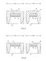
FIGS. 1 through 18 are schematic views showing the process for manufacturing a semiconductor device that has a trench-gate transistor and a planar transistor according to a first embodiment of the present invention. InFIGS. 1 through 18 , “region M” indicates the memory cell region in which the trench-gate transistor is formed, and “region PE” indicates the peripheral circuit region in which the planar transistor is formed.- First, a
thin oxide film 11shaving a thickness of approximately 1.5 to 3 nm is formed on the surface of region PE of asemiconductor substrate 10, as shown inFIG. 1 . Athick oxide film 11thaving a thickness of approximately 4.5 to 6 nm is also formed in region M and in a region (not shown) in which a power supply circuit and the like are formed, and which is a region other than region PE of the peripheral circuit region. In a specific example, a thermal oxide film having a thickness of slightly less than 6 nm is formed on the entire surface of thesemiconductor substrate 10 by thermal oxidation, the region other than region PE is covered by a resist mask, and the thermal oxide film on region PE is removed, after which the resist mask is removed, and the entire surface of thesubstrate 10 is cleaned with an acid. This cleaning removes a portion of the surface of the thermal oxide film on region M and on the region (not shown) in which a power supply circuit and the like are formed, and the thickness of the thermal oxide film is reduced to about 5 nm. Then, the entire surface is again thermal-oxidized to form athin oxide film 11shaving a thickness of about 3 nm on region PE, and a thick oxide film lit having a thickness of about 6 nm on region M and the region (not shown) in which a power supply circuit and the like are formed. Thethin oxide film 11sthereby formed is the gate insulating film of the planar transistor formed in region PE. - The thickness of the oxide film lit formed in region M herein may be equal to that of the
thin oxide film 11s.However, the oxide film lit in region M is preferably formed thick as described above so that in a case in which the gate electrode of the trench-gate transistor formed in region M is formed in a shape that protrudes further than the surface of thesemiconductor substrate 10, even when the protruding portion is misaligned with respect to thegate trench 18, high breakdown voltage can be maintained in the misaligned portion as well. Thethick oxide film 11tis also the gate insulating film of a transistor having a high breakdown voltage that is formed in a region (not shown) in which a power supply circuit and other components are formed. - In the subsequent step as shown in
FIG. 2 , a phosphorus-dopedamorphous silicon film 12 as a protective film that has a thickness of approximately 10 to 30 nm is then formed by a CVD (Chemical Vapor Deposition) method in order to protect thethin oxide film 11s.Asilicon nitride film 13 having a thickness of approximately 80 to 150 nm is then formed by an LP (Low Pressure)-CVD method. - As shown in
FIG. 3 , a resistpattern 14 is formed on each element separation region formed as a region for separating elements according to the STI (Shallow Trench Isolation) technique. - As shown in
FIG. 4 , after thesilicon nitride films 13 are patterned using the resistpatterns 14 as a mask, and the resistpatterns 14 are then removed, the phosphorus-dopedamorphous silicon films 12, thethick oxide films 11t,thethin oxide films 11s,and thesemiconductor substrate 10 are dry-etched using the patternedsilicon nitride films 13 as masks. The phosphorus-dopedamorphous silicon films 12, thethick oxide films 11t,and thethin oxide films 11sare thereby patterned, andtrenches 15 used for STI are also formed in thesemiconductor substrate 10. - A thermal oxidation treatment is then performed in order to remove the etching damage from the inner walls of the
trenches 15, after whichsilicon oxide films 16 are formed on the entire surface by an HDP (High-Density Plasma)-CVD method so as to fill in thetrenches 15, as shown inFIG. 5 . - CMP (Chemical Mechanical Polishing) is then performed using the
silicon nitride films 13 as a stopper, thesilicon oxide films 16 on thesilicon nitride films 13 are removed by polishing so that thesilicon oxide films 16 remain in thetrenches 15.Element separation regions 16iare thereby formed, as shown inFIG. 6 . - As shown in
FIG. 7 , a resistpattern 17 that is provided with a plurality of openings is then formed on region M in order to form the gate trenches of the trench-gate memory cell transistor in region M. Region PE is completely covered at this time by resistpatterns 17. Openings are also formed in the resistpattern 17 above theelement separation regions 16iof region M in order to be used for a gate trench that is formed in an adjacent memory cell region (not shown). - Using the resist
pattern 17 as a mask, thesilicon nitride film 13 is then patterned in the shape of the mask, as shown inFIG. 8 . - After the resist
pattern 17 is removed, the phosphorus-dopedamorphous silicon film 12 and thethick oxide film 11tare etched, and thesemiconductor substrate 10 is also etched, wherebygate trenches 18 are formed in thesemiconductor substrate 10, as shown inFIG. 9 . Thesilicon nitride film 13 that was used as a mask for forming theSTI trenches 15 shown inFIG. 4 thus remains without being removed, and is also used as a mask for forming thegate trenches 18, as shown inFIG. 9 . - Sacrificial oxidation is then performed by thermal oxidation to remove damage and contamination from the etched surfaces inside the
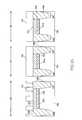
gate trenches 18, and the sacrificial oxide film is then removed by wet etching. Asilicon oxide film 19 is then formed to act as the gate insulating film of the memory cell transistor, as shown inFIG. 10 . Thissilicon oxide film 19 must also have high voltage resistance as described above, and preferably has a thickness of approximately 4.5 to 6 nm. Thesilicon oxide film 19 herein is preferably formed by a process in which a CVD oxide film (preferably a HTO (High Temperature Oxide)) having a thickness of approximately 3.5 to 5.5 nm is deposited by a CVD method at a temperature of approximately 800° C., after which the CVD oxide film is thermally oxidized at a temperature of approximately 1050° C. in order to densify the CVD oxide film, remove impurities, and modify the interface between the CVD oxide film and thesemiconductor substrate 10. The time needed to form the second gate insulating film in the gate trench can thereby be prevented from increasing even when further reduction in size narrows the opening of the gate trench, and an increase in oxidation stress can also be suppressed. - In contrast, when the full-thickness portion of the
silicon oxide film 19 is formed by thermal oxidation, not only is the oxidation time lengthened, but oxidizing species also diffuse into the interface between thesemiconductor substrate 10 and the element separation regions (STI)16i.This causes a cubical expansion because theSTI 16iare oxidized, thereby creating stress in thesemiconductor substrate 10 and adversely affecting the junction characteristics of the DRAM. Accordingly, thesilicon oxide film 19 is preferably formed according to the method described above. At this time, since thethin oxide film 11sformed on thesemiconductor substrate 10 in region PE is covered by the phosphorus-dopedamorphous silicon film 12 that is the protective film, it is possible to prevent a CVD oxide film from being deposited on thethin oxide film 11s,and to prevent thethin oxide film 11sfrom becoming thicker as a result of thermal oxidation. - In order to form the gate electrode of the trench-gate transistor, an amorphous silicon film that is doped with phosphorus as an N-type impurity is then formed on the entire surface that includes the insides of the
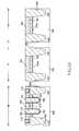
gate trenches 18. Phosphorus-dopedamorphous silicon films 20 are then embedded in thegate trenches 18 as shown inFIG. 11 , by performing a planarization process according to a CMP method in which thesilicon nitride film 13 is used as a stopper. - The phosphorus-doped
amorphous silicon films 20 in thegate trenches 18 are then etched back to about the same position as thethick oxide film 11tby dry etching, as shown inFIG. 12 . - Wet etching is then performed to remove the
silicon nitride film 13, the upper portions of theelement separation regions 16i,and the upper portions of thesilicon oxide films 19. The upper surfaces of theelement separation regions 16iand the phosphorus-dopedamorphous silicon film 12 are thereby aligned with each other, as shown inFIG. 13 . In this arrangement, the phosphorus-dopedamorphous silicon film 12 is formed on thegate insulating film 11sin region PE, and is made to function as a protective film when the nitride film13 (seeFIG. 12 ) used as a mask for forming thegate trench 18 is removed. It is therefore possible to prevent thegate insulating film 11sfrom being damaged. - A CVD method is then used to form an amorphous silicon film (phosphorus-doped amorphous silicon film)21 that is doped with phosphorus as an N-type impurity and has a thickness of approximately 30 to 80 nm on the entire surface, as shown in
FIG. 14 . - A resist
pattern 22 used to form a gate electrode is then formed on the phosphorus-dopedamorphous silicon film 21, as shown inFIG. 15 . - The phosphorus-doped
amorphous silicon film 21 is then patterned using a resistpattern 22 as a mask, as shown inFIG. 16 . A gate electrode of a trench-gate transistor composed of the phosphorus-dopedamorphous silicon films amorphous silicon films - The example described herein is of a case in which the patterned
amorphous silicon films 21 are not misaligned with respect to thegate trenches 18 in region M. However, when misalignment does occur, theamorphous silicon films 21 remain on the thick oxide film lit and become portions of a gate electrode. In this type of case, thethick oxide film 11tfunctions as a portion of the gate insulating film in this trench-gate transistor. However, since the oxide filmtis formed so as to have about the same thickness as thesilicon oxide films 19 in thegate trenches 18, a reduction in the breakdown voltage thereof can be minimized. - N-type source/
drain diffusion regions 23 are formed in region M, and N-type source/drain diffusion regions 24 are formed in region PE by ion implantation of an N-type impurity into regions M and PE using each gate electrode as a mask, as shown inFIG. 17 . A trench-gate memory cell transistor is thereby formed in region M, and a planar transistor is formed in region PE. - The
amorphous silicon films - Various types of wiring or cell capacitors are then layered in region M using a common method. Specifically, DRAM having a trench-gate memory cell transistor is formed by a process in which an
interlayer insulating film 25 is formed on the memory cell transistor, and acontact plug 26 that pass through theinterlayer insulating film 25, abit line 27, acell capacitor 28,Al wiring 29, and other components are formed, as shown inFIG. 18 . - In the present embodiment as described above, a
thin oxide film 11sis formed in advance to function as the gate insulating film of the planar transistor on thesemiconductor substrate 10 of the peripheral circuit region PE, and thisthin oxide film 11sis covered by theamorphous silicon film 12. In this state, agate trench 18 is formed in memory cell region M, and agate insulating film 19 that is thicker than thegate insulating film 11sis formed on the inner wall of thegate trench 18. Since theamorphous silicon film 12 thereby functions as a protective film for preventing growth of thegate insulating film 11s,thegate insulating film 19 can be made thick while thegate insulating film 11sremains thin. Specifically, thegate insulating film 11sand thegate insulating film 19 can be formed independently of each other. The number of oxidation steps performed in thegate trench 18 can therefore be reduced. - According to the present embodiment, oxidation stress in the
gate trench 18 can be reduced, and a degradation of the refresh characteristics can be prevented. Since thegate insulating film 11sand thegate insulating film 19 are formed independently rather than simultaneously, the film thickness and other characteristics are easily controlled. - As a second embodiment, an example will next be described in which the present invention is applied when a trench-gate transistor having a thick oxide film as the gate insulating film is formed in the memory cell region in the same manner as in the first embodiment, and a dual-gate-structured transistor having a thin oxide film as the gate insulating film is formed in the peripheral circuit region. In a dual-gate structure, a gate electrode that includes N-type polycrystalline silicon into which an N-type impurity (phosphorus or the like) is introduced is used as the gate electrode of an N-channel transistor, and a gate electrode that includes P-type polycrystalline silicon into which a P-type impurity (boron or the like) is introduced is used in a P-channel transistor.
FIGS. 19 through 38 are schematic views showing the process for manufacturing a semiconductor device that has a trench-gate transistor and a dual-gate-structured transistor according to a second embodiment of the present invention. InFIGS. 19 through 38 , “region M” indicates the memory cell region in which the trench-gate transistor is formed, and “region P” and “region N” are provided to the peripheral circuit region, wherein “region P” is a region (also referred to as a P-type peripheral circuit region) in which a planar P-channel transistor provided with a gate electrode that includes P-type polycrystalline silicon is formed, and “region N” is a region (also referred to as an N-type peripheral circuit region) in which a planar N-channel transistor provided with a gate electrode that includes N-type polycrystalline silicon is formed.- First, a
thin oxide film 101shaving a thickness of approximately 1.5 to 3 nm is formed on the surface of regions P and N of asemiconductor substrate 100, as shown inFIG. 19 . Athick oxide film 101thaving a thickness of approximately 4.5 to 6 nm is also formed in region M and in a region (not shown) in which a power supply circuit and the like are formed, and which is a region other than region P or N of the peripheral circuit region. Specifically, thethin oxide film 101sand thethick oxide film 101tare formed in the same manner as thethin oxide film 11sand the thick oxide filmtin the process shown inFIG. 1 in the abovementioned first embodiment. Thethin oxide film 101sthus formed is the gate insulating film of a dual-gate-structured planar transistor formed in regions P and N. - The thickness of the
oxide film 101tformed in region M may be the same as that of thethin oxide film 101s,but a thick film is preferred for the same reason as in the first embodiment. Thethick oxide film 101tis the gate insulating film of a transistor having a high breakdown voltage that is formed in a region (not shown) in which a power supply circuit and other components are formed, the same as thethick oxide film 11tin the first embodiment. - In the subsequent step as shown in
FIG. 20 , a non-dopedamorphous silicon film 102 as a protective film that has a thickness of approximately 10 to 30 nm is then formed by a CVD (Chemical Vapor Deposition) method in order to protect thethin oxide film 101s.In the present embodiment, since a dual-gate-structured transistor is formed in regions P and N of the peripheral circuit region, a non-doped amorphous silicon film is used as the protective film instead of the doped amorphous silicon film used in the abovementioned first embodiment. Asilicon nitride film 103 having a thickness of approximately 80 to 150 nm is then formed by an LP (Low Pressure)-CVD method. - As shown in
FIG. 21 , a resistpattern 104 is formed on each element separation region formed as a region for separating elements according to the STI (Shallow Trench Isolation) technique. - As shown in
FIG. 22 , after thesilicon nitride films 103 are patterned using the resistpatterns 104 as a mask, and the resistpatterns 104 are then removed, the non-dopedamorphous silicon films 102, thethick oxide films 101t,thethin oxide films 101s,and thesemiconductor substrate 100 are dry-etched using the patternedsilicon nitride films 103 as masks. The non-dopedamorphous silicon films 102, thethick oxide films 101t,and thethin oxide films 101sare thereby patterned, andtrenches 105 used for STI are also formed in thesemiconductor substrate 100. - A thermal oxidation treatment is then performed in order to remove the etching damage from the inner walls of the
trenches 105, after whichsilicon oxide films 106 are formed on the entire surface by an HDP (High-Density Plasma)-CVD method so as to fill in thetrenches 105, as shown inFIG. 23 . - CMP (Chemical Mechanical Polishing) is then performed using the
silicon nitride films 103 as a stopper, thesilicon oxide films 106 on thesilicon nitride films 103 are removed by polishing so that thesilicon oxide films 106 remain in thetrenches 105.Element separation regions 106iare thereby formed, as shown inFIG. 24 . - As shown in
FIG. 25 , a resistpattern 107 that is provided with a plurality of openings is then formed on region M in order to form the gate trenches of the trench-gate memory cell transistor in region M. Regions P and N are completely covered at this time by resistpatterns 107. - Using the resist
pattern 107 as a mask, thesilicon nitride film 103 is then patterned in the shape of the mask, as shown inFIG. 26 . - After the resist
pattern 107 is removed, the non-dopedamorphous silicon film 102 and thethick oxide film 101tare etched, and thesemiconductor substrate 100 is also etched, wherebygate trenches 108 are formed in thesemiconductor substrate 100, as shown inFIG. 27 . Thesilicon nitride film 103 that was used as a mask for forming theSTI trenches 105 shown inFIG. 22 thus remains without being removed, and is also used as a mask for forming thegate trenches 108, as shown inFIG. 27 . - Sacrificial oxidation is then performed by thermal oxidation to remove damage and contamination from the etched surfaces inside the
gate trenches 108, and the sacrificial oxide film is then removed by wet etching. Asilicon oxide film 109 is then formed to act as the gate insulating film of the memory cell transistor, as shown inFIG. 28 . Thissilicon oxide film 109 is the gate insulating film of the memory cell transistor, and therefore must have a high breakdown voltage, as in the first embodiment, and the thickness thereof is preferably about B4.5 to 6 nm. Thissilicon oxide film 109 can be formed in the same manner as thesilicon oxide film 19 formed in the steps of the first embodiment shown inFIG. 10 . Thethin oxide film 101sformed on thesemiconductor substrate 100 of regions P and N is covered at this time by a non-dopedamorphous silicon film 102, which is a protective film. It is therefore possible to prevent an oxide film from being further deposited on thethin oxide film 101s,and to prevent thethin oxide film 101sfrom increasing in thickness due to thermal oxidation. - In order to form the gate electrode of the trench-gate transistor, an amorphous silicon film that is doped with phosphorus as an N-type impurity is then formed on the entire surface that includes the insides of the
gate trenches 108. Phosphorus-dopedamorphous silicon films 110 are then embedded in thegate trenches 108 as shown inFIG. 29 , by performing a planarization process according to a CMP method in which thesilicon nitride film 103 is used as a stopper. - The phosphorus-doped
amorphous silicon films 110 in thegate trenches 108 are then etched back to about the same position as thethick oxide film 101tby dry etching, as shown inFIG. 30 . - Wet etching is then performed to remove the
silicon nitride film 103, the upper portions of theelement separation regions 106i,and the upper portions of thesilicon oxide films 109. The upper surfaces of theelement separation regions 106iand the protective film (non-doped amorphous silicon film)102 are thereby aligned with each other, as shown inFIG. 31 . - A CVD method is then used to form a non-doped
amorphous silicon film 111 having a thickness of approximately 30 to 80 nm to become the gate electrode of the dual-gate transistor, as shown inFIG. 32 . Also unlike the abovementioned first embodiment, a dual-gate-structured transistor is formed in regions P and N in the present embodiment. A non-doped amorphous silicon film is therefore used instead of a doped amorphous silicon film as the film for forming the gate electrode. - As shown in
FIG. 33 , regions M and N are then masked by a resistpattern 112, and boron (B) as a P-type impurity is ion-implanted into region P. This ion implantation of boron is performed at a low energy of 10 keV or less. The implanted boron ions are diffused in a subsequently performed heat treatment, whereby the non-dopedamorphous silicon films 111 and102 (seeFIG. 32 ) of region P become P-typeamorphous silicon films - After the resist
pattern 112 is removed, region P in this instance is masked by a resistpattern 113, and phosphorus (P) as an N-type impurity is ion-implanted into regions M and N, as shown inFIG. 34 . This ion implantation of phosphorus is also performed at a low energy of 20 keV or less, the same as the ion implantation of boron described above, and the phosphorus ions are diffused by a subsequent heat treatment. The non-dopedamorphous silicon films 111 and102 (seeFIG. 33 ) of region N thereby become N-typeamorphous silicon films amorphous silicon films amorphous silicon films - According to the present embodiment, phosphorus-doped
silicon films 110 are already embedded in thegate trenches 108 of region M. Ion implantation can therefore be performed under suitable implantation conditions according to the thickness of thesilicon film 111 and thesilicon film 102 without regard to implantation into thegate trenches 108 when ion implantation into region M is performed at the same time as phosphorus is implanted into region N in the ion implantation process for creating P-type and N-typenon-doped silicon films 111, which are the gate electrodes of the dual-gate transistor. - Resist
patterns 114 for use in forming gate electrodes are then formed on the impurity-dopedamorphous silicon films FIG. 35 . - As shown in
FIG. 36 , the layered film that includes theamorphous silicon films amorphous silicon films pattern 114 as a mask. A gate electrode of a trench-gate transistor composed of dopedamorphous silicon films amorphous silicon films amorphous silicon films - As shown in
FIG. 37 , regions M and N are then covered by a resist film (not shown), and P-type source/drain diffusion regions 115pare formed by ion-implanting a P-type impurity into region P using the P-type gate electrode as a mask. Region P is then covered by a resist film (not shown), and an N-type impurity is ion-implanted into regions M and N using the gate electrodes of regions M and N as masks. N-type source/drain diffusion regions 115nare thereby formed in region N, and N-type source/drain diffusion regions 116 are formed in region M. According to this process, a trench-gate memory cell transistor is formed in region M, and a dual-gate transistor is formed in regions P and N, which are peripheral circuit regions. - The
amorphous silicon films - Various types of wiring or cell capacitors are then layered in region M using a common method similar to the first embodiment. Specifically, DRAM having a trench-gate memory cell transistor is formed by a process in which an
interlayer insulating film 117 is formed on the memory cell transistor, and acontact plug 118 that pass through theinterlayer insulating film 117, abit line 119, acell capacitor 120, Al wiring121, and other components are formed, as shown inFIG. 38 . - According to the present embodiment as described above, a
thin oxide film 101sis formed in advance on thesemiconductor substrate 100 of regions P and N in the peripheral circuit region to become the gate insulating film of the dual-gate-structured transistor that is formed in regions P and N.A gate trench 108 is then formed in the memory cell region M in a state in which thethin oxide film 101sis covered by anamorphous silicon film 102, and agate insulating film 109 that is thicker than thegate insulating film 101sis formed on the inner wall of thegate trench 108, whereby thegate insulating film 101sand thegate insulating film 109 can be formed independently of each other. The same effects as those of the abovementioned first embodiment are thereby obtained. - Furthermore, according to the present embodiment, an
amorphous silicon film 110 that is selectively doped with an impurity can be formed in thegate trench 108 of region M. Specifically, the following processes are involved in an example of a possible method for selectively forming doped silicon in the gate trench when a trench-gate transistor and a dual-gate-structured transistor are formed on the same substrate. After a gate trench is formed in a semiconductor substrate, a thermal oxide film serving as the gate insulating film of the transistors is formed in the gate trench and on the semiconductor substrate in the peripheral circuit region in which the dual-gate-structured transistor is formed, and a doped silicon film is formed on the entire surface that includes the inside of the gate trench. The doped silicon film is then etched back so as to remain only in the gate trench, a non-doped silicon film is formed on the gate insulating film to be used for the gate electrode of the dual-gate-structured transistor, and P- and N-type gate electrodes are each formed by ion implantation. - However, in this method, the gate insulating film of the dual-gate-structured transistor is usually damaged when the doped silicon is etched back, making it difficult to form a high-performance transistor. In the present embodiment, however, a non-doped
amorphous silicon film 102 is formed on thegate insulating film 101son regions P and N, which are the regions in which the dual-gate-structured transistor is formed, in the step for removing thesilicon nitride film 103 that is used as a mask for forming thegate trench 108, thegate insulating film 109, the dopedsilicon film 110 that is embedded in thegate trench 108, and thegate trench 108. Damage to thegate insulating film 101scan thereby be prevented when themask nitride film 103 is removed. - Accordingly, it is possible to form an impurity-doped
amorphous silicon film 110 in thegate trench 108, and to form a non-dopedamorphous silicon film 111 on regions P and N as well as on the dopedamorphous silicon film 110 that was embedded in the gate trenches. Thesilicon films gate insulating film 101s,and the trench-gate transistor and the dual-gate-structured transistor can both be endowed with high performance. - As described above, an
amorphous silicon film 110 that is selectively doped with an impurity can be formed in thegate trench 108. Depletion of the trench-gate electrode can thereby be prevented in contrast to a case in which an impurity is introduced after a non-doped silicon film is formed in the gate trench. - The present invention is in no way limited to the aforementioned embodiments, but rather various modifications are possible within the scope of the invention as recited in the claims, and naturally these modifications are included within the scope of the invention.
- For example, in the abovementioned embodiments, the protective film used for covering the
thin oxide film 11s(101s) was a dopedamorphous silicon film 12 in the first embodiment, and a non-dopedamorphous silicon film 102 in the second embodiment. However, these configurations are not limiting, and another material may also be used insofar as the resulting film can prevent an oxide film from being layered on thethin oxide film 11s(101s) when the gate insulating film19 (109) is formed in the gate trench18 (108), or thickness from being increased due to further oxidation, while the operation of the transistors is not impeded. Specifically, another material may be used insofar as the resulting film (conductive thin film or the like) allows formation of a channel needed during the application of voltage to a gate electrode. - In the abovementioned embodiment, an example was described in which each silicon film was first formed in an amorphous state and then converted to a polycrystalline silicon film by a subsequent heating process. However, polycrystalline silicon films may also be used initially as needed.
- In the embodiments described above, a layered film that included silicon films12 (102) and21 (111) was used as the gate electrode of the planar transistor, but the silicon film12 (102), which is a protective film, may be formed in advance so as to initially have the required thickness as a gate electrode in cases in which the
gate trench 108 or the STI trench15 (105) has a small depth, and in other cases. - The gate electrode is also not necessarily formed using only silicon films, and it is also possible to form a silicide layer on a silicon film, or to create a so-called polymetal gate electrode by layering metal films.
- Furthermore, the example described above was one in which the mask layer for forming the trenches15 (105) that were used for STI, and the mask layer for forming the gate trenches18 (108) were used in common in the silicon nitride film13 (103). However, the silicon nitride film13 (103) may be removed after the STI (element separation regions)16i(106i) are formed, and a new silicon nitride film may be created to form a mask layer.
Claims (12)
Priority Applications (1)
| Application Number | Priority Date | Filing Date | Title |
|---|---|---|---|
| US12/905,687US20110034005A1 (en) | 2005-10-28 | 2010-10-15 | Method for manufacturing semiconductor device |
Applications Claiming Priority (2)
| Application Number | Priority Date | Filing Date | Title |
|---|---|---|---|
| JP2005-313661 | 2005-10-28 | ||
| JP2005313661AJP4773182B2 (en) | 2005-10-28 | 2005-10-28 | Manufacturing method of semiconductor device |
Related Child Applications (2)
| Application Number | Title | Priority Date | Filing Date |
|---|---|---|---|
| US12/797,179ContinuationUS8865683B2 (en) | 2003-12-04 | 2010-06-09 | Active compound combinations having insecticidal properties |
| US12/905,687DivisionUS20110034005A1 (en) | 2005-10-28 | 2010-10-15 | Method for manufacturing semiconductor device |
Publications (2)
| Publication Number | Publication Date |
|---|---|
| US20070096204A1true US20070096204A1 (en) | 2007-05-03 |
| US7935595B2 US7935595B2 (en) | 2011-05-03 |
Family
ID=37995129
Family Applications (2)
| Application Number | Title | Priority Date | Filing Date |
|---|---|---|---|
| US11/581,346Active2029-08-03US7935595B2 (en) | 2005-10-28 | 2006-10-17 | Method for manufacturing semiconductor device |
| US12/905,687AbandonedUS20110034005A1 (en) | 2005-10-28 | 2010-10-15 | Method for manufacturing semiconductor device |
Family Applications After (1)
| Application Number | Title | Priority Date | Filing Date |
|---|---|---|---|
| US12/905,687AbandonedUS20110034005A1 (en) | 2005-10-28 | 2010-10-15 | Method for manufacturing semiconductor device |
Country Status (4)
| Country | Link |
|---|---|
| US (2) | US7935595B2 (en) |
| JP (1) | JP4773182B2 (en) |
| CN (1) | CN100447985C (en) |
| TW (1) | TWI318439B (en) |
Cited By (28)
| Publication number | Priority date | Publication date | Assignee | Title |
|---|---|---|---|---|
| US20070099381A1 (en)* | 2005-08-03 | 2007-05-03 | Walker Andrew J | Dual-gate device and method |
| US20080042179A1 (en)* | 2006-08-21 | 2008-02-21 | Micron Technology, Inc. | Memory arrays and methods of fabricating memory arrays |
| US20080142882A1 (en)* | 2004-09-01 | 2008-06-19 | Tang Sanh D | Transistors |
| US20080160700A1 (en)* | 2006-12-29 | 2008-07-03 | Hynix Semiconductor Inc. | Method For Manufacturing Semiconductor Device Having Bulb-Type Recessed Channel |
| US20090047766A1 (en)* | 2007-08-14 | 2009-02-19 | Shian-Jyh Lin | Method for fabricating recess channel mos transistor device |
| US20090242980A1 (en)* | 2008-03-25 | 2009-10-01 | Nec Electronics Corporation | Semiconductor device including capacitor element and method of manufacturing the same |
| US20090311845A1 (en)* | 2006-09-07 | 2009-12-17 | Micron Technology, Inc. | One Transistor Memory Cell with Bias Gate |
| US20100006932A1 (en)* | 2008-07-09 | 2010-01-14 | Nec Electronics Corporation | Semiconductor device and method of manufacturing the same |
| US20100072545A1 (en)* | 2008-09-22 | 2010-03-25 | Jeong-Do Ryu | Recessed Channel Array Transistors, and Semiconductor Devices Including a Recessed Channel Array Transistor |
| US7700441B2 (en) | 2006-02-02 | 2010-04-20 | Micron Technology, Inc. | Methods of forming field effect transistors, methods of forming field effect transistor gates, methods of forming integrated circuitry comprising a transistor gate array and circuitry peripheral to the gate array, and methods of forming integrated circuitry comprising a transistor gate array including first gates and second grounded isolation gates |
| US20100258858A1 (en)* | 2009-04-10 | 2010-10-14 | Hynix Semiconductor Inc. | Method of fabricating semiconductor device |
| US20100270603A1 (en)* | 2009-04-22 | 2010-10-28 | Hynix Semiconductor Inc. | Semiconductor device and method of manufacturing the same |
| CN101908542A (en)* | 2009-06-03 | 2010-12-08 | 索尼公司 | Semiconductor device, manufacturing method thereof, and solid-state imaging element |
| US7867851B2 (en) | 2005-08-30 | 2011-01-11 | Micron Technology, Inc. | Methods of forming field effect transistors on substrates |
| US20110034005A1 (en)* | 2005-10-28 | 2011-02-10 | Elpida Memory, Inc. | Method for manufacturing semiconductor device |
| US7897460B2 (en) | 2005-03-25 | 2011-03-01 | Micron Technology, Inc. | Methods of forming recessed access devices associated with semiconductor constructions |
| US20110140186A1 (en)* | 2009-12-11 | 2011-06-16 | Dongbu Hitek Co., Ltd. | Capacitor for semiconductor device and manufacturing method of capacitor for semiconductor device |
| US20110237037A1 (en)* | 2008-09-22 | 2011-09-29 | Samsung Electronics Co., Ltd. | Methods of Forming Recessed Channel Array Transistors and Methods of Manufacturing Semiconductor Devices |
| US8399920B2 (en) | 2005-07-08 | 2013-03-19 | Werner Juengling | Semiconductor device comprising a transistor gate having multiple vertically oriented sidewalls |
| US8476701B2 (en)* | 2010-05-19 | 2013-07-02 | Renesas Electronics Corporation | Semiconductor device with gate electrode including a concave portion |
| US8552372B2 (en) | 2011-05-19 | 2013-10-08 | Elpida Memory, Inc. | Method and system of evaluating distribution of lattice strain on crystal material |
| US8551823B2 (en) | 2006-07-17 | 2013-10-08 | Micron Technology, Inc. | Methods of forming lines of capacitorless one transistor DRAM cells, methods of patterning substrates, and methods of forming two conductive lines |
| US8835254B2 (en) | 2011-06-30 | 2014-09-16 | Fuji Electric Co., Ltd. | Semiconductor device manufacturing method |
| US20150008479A1 (en)* | 2012-02-14 | 2015-01-08 | Toyota Jidosha Kabushiki Kaisha | Igbt and igbt manufacturing method |
| US20150017774A1 (en)* | 2013-07-10 | 2015-01-15 | Globalfoundries Inc. | Method of forming fins with recess shapes |
| US8993391B2 (en)* | 2012-12-27 | 2015-03-31 | SK Hynix Inc. | Semiconductor device with recess gate and method for fabricating the same |
| US10515801B2 (en) | 2007-06-04 | 2019-12-24 | Micron Technology, Inc. | Pitch multiplication using self-assembling materials |
| US20220285344A1 (en)* | 2020-03-13 | 2022-09-08 | Taiwan Semiconductor Manufacturing Company, Ltd. | Method to embed planar fets with finfets |
Families Citing this family (20)
| Publication number | Priority date | Publication date | Assignee | Title |
|---|---|---|---|---|
| US7595262B2 (en)* | 2006-10-27 | 2009-09-29 | Qimonda Ag | Manufacturing method for an integrated semiconductor structure |
| JP2009076575A (en)* | 2007-09-19 | 2009-04-09 | Elpida Memory Inc | Manufacturing method of semiconductor device |
| JP2009182114A (en)* | 2008-01-30 | 2009-08-13 | Elpida Memory Inc | Semiconductor device and manufacturing method thereof |
| KR20090087645A (en) | 2008-02-13 | 2009-08-18 | 삼성전자주식회사 | Method of manufacturing semiconductor device having recess channel array transistor |
| KR101535222B1 (en)* | 2008-04-17 | 2015-07-08 | 삼성전자주식회사 | Semiconductor device and method of fabricating the same |
| KR20100033918A (en)* | 2008-09-22 | 2010-03-31 | 삼성전자주식회사 | Recessed channel array transistor and method of forming the same, semiconductor device and method of manufacturing the semiconductor device |
| JP4862878B2 (en)* | 2008-10-30 | 2012-01-25 | ソニー株式会社 | Solid-state imaging device, manufacturing method thereof, and imaging device |
| JP5407282B2 (en)* | 2008-11-07 | 2014-02-05 | ソニー株式会社 | SOLID-STATE IMAGING DEVICE, ITS MANUFACTURING METHOD, AND ELECTRONIC DEVICE |
| KR101075526B1 (en)* | 2009-07-03 | 2011-10-20 | 주식회사 하이닉스반도체 | Method for forming self aligned contact in semiconductor device with buried gate |
| KR101096875B1 (en)* | 2009-12-09 | 2011-12-22 | 주식회사 하이닉스반도체 | Method for manufacturing semiconductor having buried gate |
| KR101061296B1 (en)* | 2010-07-01 | 2011-08-31 | 주식회사 하이닉스반도체 | Semiconductor element and method of forming the same |
| US10096696B2 (en)* | 2014-06-03 | 2018-10-09 | Micron Technology, Inc. | Field effect transistors having a fin |
| TWI555120B (en)* | 2014-10-14 | 2016-10-21 | 力晶科技股份有限公司 | Semiconductor component and manufacturing method thereof |
| KR102316160B1 (en)* | 2014-12-22 | 2021-10-26 | 삼성전자주식회사 | Semiconductor device and method of manufacturing the same |
| US20160211348A1 (en)* | 2015-01-21 | 2016-07-21 | Maxchip Electronics Corp. | Trench lateral diffusion metal oxide semiconductor device and manufacturing method of the same |
| US9768175B2 (en) | 2015-06-21 | 2017-09-19 | Micron Technology, Inc. | Semiconductor devices comprising gate structure sidewalls having different angles |
| CN113678253B (en) | 2021-06-30 | 2025-03-18 | 长江存储科技有限责任公司 | Peripheral circuit with recessed gate transistor and method of forming the same |
| CN113632169B (en)* | 2021-06-30 | 2024-06-18 | 长江存储科技有限责任公司 | Peripheral circuit with recessed gate transistor and method of forming the same |
| US11848048B2 (en)* | 2021-11-30 | 2023-12-19 | Micron Technology, Inc. | Memory device decoder configurations |
| US20250016997A1 (en)* | 2023-07-05 | 2025-01-09 | Nanya Technology Corporation | Semiconductor structure and method of manufacturing the same |
Citations (19)
| Publication number | Priority date | Publication date | Assignee | Title |
|---|---|---|---|---|
| US6063669A (en)* | 1996-02-26 | 2000-05-16 | Nec Corporation | Manufacturing method of semiconductor memory device having a trench gate electrode |
| US20010025973A1 (en)* | 2000-01-25 | 2001-10-04 | Satoru Yamada | Semiconductor integrated circuit device and process for manufacturing the same |
| US6317360B1 (en)* | 1998-09-01 | 2001-11-13 | Nec Corporation | Flash memory and methods of writing and erasing the same as well as a method of forming the same |
| US20020195647A1 (en)* | 2001-06-26 | 2002-12-26 | Seiichi Aritome | Nonvolatile semiconductor memory and manufacturing method thereof |
| US6913964B2 (en)* | 2002-03-11 | 2005-07-05 | Monolithic System Technology, Inc. | Method of fabricating a one transistor floating-body DRAM cell in bulk CMOS process with electrically isolated charge storage region |
| US6964895B2 (en)* | 2002-03-11 | 2005-11-15 | Monolithic System Technology, Inc. | Method of fabricating vertical one-transistor floating-body DRAM cell in bulk CMOS process with electrically isolated charge storage region |
| US7078296B2 (en)* | 2002-01-16 | 2006-07-18 | Fairchild Semiconductor Corporation | Self-aligned trench MOSFETs and methods for making the same |
| US7116583B2 (en)* | 2004-04-13 | 2006-10-03 | Infineon Technoloiges Ag | Electrically programmable memory cell and methods for programming and reading from such a memory cell |
| US7132325B2 (en)* | 2001-11-20 | 2006-11-07 | International Business Machines Corporation | Test structure and methodology for semiconductor stress-induced defects and antifuse based on same test structure |
| US20070082440A1 (en)* | 2005-10-11 | 2007-04-12 | Elpida Memory, Inc. | Semiconductor device and manufacturing method thereof |
| US7396738B1 (en)* | 2006-12-13 | 2008-07-08 | Hynix Semiconductor Inc. | Method of forming isolation structure of flash memory device |
| US7432139B2 (en)* | 2005-06-29 | 2008-10-07 | Amberwave Systems Corp. | Methods for forming dielectrics and metal electrodes |
| US7482223B2 (en)* | 2004-12-22 | 2009-01-27 | Sandisk Corporation | Multi-thickness dielectric for semiconductor memory |
| US7560359B2 (en)* | 2004-11-26 | 2009-07-14 | Samsung Electronics Co., Ltd. | Methods of forming asymmetric recesses and gate structures that fill such recesses and related methods of forming semiconductor devices that include such recesses and gate structures |
| US7619281B2 (en)* | 2006-10-02 | 2009-11-17 | Samsung Electronics Co., Ltd. | Semiconductor device having buried gate line and method of fabricating the same |
| US7701002B2 (en)* | 2006-06-28 | 2010-04-20 | Samsung Electronics Co., Ltd. | Semiconductor device having buried gate electrode and method of fabricating the same |
| US7700979B2 (en)* | 2006-03-21 | 2010-04-20 | Hynix Semiconductor Inc. | Semiconductor device having bulb-shaped recess gate and method for fabricating the same |
| US7713873B2 (en)* | 2007-05-16 | 2010-05-11 | Samsung Electronics Co., Ltd. | Methods of forming contact structures semiconductor devices |
| US7714384B2 (en)* | 2003-09-15 | 2010-05-11 | Seliskar John J | Castellated gate MOSFET device capable of fully-depleted operation |
Family Cites Families (9)
| Publication number | Priority date | Publication date | Assignee | Title |
|---|---|---|---|---|
| JP3150496B2 (en) | 1993-06-30 | 2001-03-26 | 株式会社東芝 | Semiconductor storage device |
| JP4322477B2 (en)* | 2001-06-28 | 2009-09-02 | 株式会社東芝 | Manufacturing method of semiconductor device |
| JP2003174158A (en)* | 2001-12-07 | 2003-06-20 | Sony Corp | Manufacturing method for semiconductor device |
| WO2003103036A1 (en)* | 2002-05-31 | 2003-12-11 | Koninklijke Philips Electronics N.V. | Trench-gate semiconductor device and method of manufacturing |
| JP4319809B2 (en) | 2002-06-05 | 2009-08-26 | 株式会社デンソー | Manufacturing method of semiconductor device |
| JP2004022915A (en)* | 2002-06-19 | 2004-01-22 | Hitachi Ltd | Method for manufacturing semiconductor integrated circuit device |
| KR100511045B1 (en)* | 2003-07-14 | 2005-08-30 | 삼성전자주식회사 | Integration method of a semiconductor device having a recessed gate electrode |
| JP2005142203A (en) | 2003-11-04 | 2005-06-02 | Elpida Memory Inc | Semiconductor device and manufacturing method thereof |
| JP4773182B2 (en)* | 2005-10-28 | 2011-09-14 | エルピーダメモリ株式会社 | Manufacturing method of semiconductor device |
- 2005
- 2005-10-28JPJP2005313661Apatent/JP4773182B2/enactiveActive
- 2006
- 2006-10-17USUS11/581,346patent/US7935595B2/enactiveActive
- 2006-10-26TWTW095139553Apatent/TWI318439B/enactive
- 2006-10-30CNCNB2006101428341Apatent/CN100447985C/enactiveActive
- 2010
- 2010-10-15USUS12/905,687patent/US20110034005A1/ennot_activeAbandoned
Patent Citations (21)
| Publication number | Priority date | Publication date | Assignee | Title |
|---|---|---|---|---|
| US6063669A (en)* | 1996-02-26 | 2000-05-16 | Nec Corporation | Manufacturing method of semiconductor memory device having a trench gate electrode |
| US6317360B1 (en)* | 1998-09-01 | 2001-11-13 | Nec Corporation | Flash memory and methods of writing and erasing the same as well as a method of forming the same |
| US20010025973A1 (en)* | 2000-01-25 | 2001-10-04 | Satoru Yamada | Semiconductor integrated circuit device and process for manufacturing the same |
| US6770535B2 (en)* | 2000-01-25 | 2004-08-03 | Hitachi, Ltd. | Semiconductor integrated circuit device and process for manufacturing the same |
| US20020195647A1 (en)* | 2001-06-26 | 2002-12-26 | Seiichi Aritome | Nonvolatile semiconductor memory and manufacturing method thereof |
| US7132325B2 (en)* | 2001-11-20 | 2006-11-07 | International Business Machines Corporation | Test structure and methodology for semiconductor stress-induced defects and antifuse based on same test structure |
| US7078296B2 (en)* | 2002-01-16 | 2006-07-18 | Fairchild Semiconductor Corporation | Self-aligned trench MOSFETs and methods for making the same |
| US6964895B2 (en)* | 2002-03-11 | 2005-11-15 | Monolithic System Technology, Inc. | Method of fabricating vertical one-transistor floating-body DRAM cell in bulk CMOS process with electrically isolated charge storage region |
| US6913964B2 (en)* | 2002-03-11 | 2005-07-05 | Monolithic System Technology, Inc. | Method of fabricating a one transistor floating-body DRAM cell in bulk CMOS process with electrically isolated charge storage region |
| US7714384B2 (en)* | 2003-09-15 | 2010-05-11 | Seliskar John J | Castellated gate MOSFET device capable of fully-depleted operation |
| US7116583B2 (en)* | 2004-04-13 | 2006-10-03 | Infineon Technoloiges Ag | Electrically programmable memory cell and methods for programming and reading from such a memory cell |
| US7560359B2 (en)* | 2004-11-26 | 2009-07-14 | Samsung Electronics Co., Ltd. | Methods of forming asymmetric recesses and gate structures that fill such recesses and related methods of forming semiconductor devices that include such recesses and gate structures |
| US7482223B2 (en)* | 2004-12-22 | 2009-01-27 | Sandisk Corporation | Multi-thickness dielectric for semiconductor memory |
| US7432139B2 (en)* | 2005-06-29 | 2008-10-07 | Amberwave Systems Corp. | Methods for forming dielectrics and metal electrodes |
| US20070082440A1 (en)* | 2005-10-11 | 2007-04-12 | Elpida Memory, Inc. | Semiconductor device and manufacturing method thereof |
| US7709324B2 (en)* | 2005-10-11 | 2010-05-04 | Elpida Memory, Inc. | Method for forming a gate within a trench including the use of a protective film |
| US7700979B2 (en)* | 2006-03-21 | 2010-04-20 | Hynix Semiconductor Inc. | Semiconductor device having bulb-shaped recess gate and method for fabricating the same |
| US7701002B2 (en)* | 2006-06-28 | 2010-04-20 | Samsung Electronics Co., Ltd. | Semiconductor device having buried gate electrode and method of fabricating the same |
| US7619281B2 (en)* | 2006-10-02 | 2009-11-17 | Samsung Electronics Co., Ltd. | Semiconductor device having buried gate line and method of fabricating the same |
| US7396738B1 (en)* | 2006-12-13 | 2008-07-08 | Hynix Semiconductor Inc. | Method of forming isolation structure of flash memory device |
| US7713873B2 (en)* | 2007-05-16 | 2010-05-11 | Samsung Electronics Co., Ltd. | Methods of forming contact structures semiconductor devices |
Cited By (60)
| Publication number | Priority date | Publication date | Assignee | Title |
|---|---|---|---|---|
| US8120101B2 (en) | 2004-09-01 | 2012-02-21 | Micron Technology, Inc. | Semiconductor constructions and transistors, and methods of forming semiconductor constructions and transistors |
| US20080142882A1 (en)* | 2004-09-01 | 2008-06-19 | Tang Sanh D | Transistors |
| US7825462B2 (en) | 2004-09-01 | 2010-11-02 | Micron Technology, Inc. | Transistors |
| US20110012182A1 (en)* | 2004-09-01 | 2011-01-20 | Micron Technology Inc. | Semiconductor Constructions and Transistors, and Methods of Forming Semiconductor Constructions and Transistors |
| US7897460B2 (en) | 2005-03-25 | 2011-03-01 | Micron Technology, Inc. | Methods of forming recessed access devices associated with semiconductor constructions |
| US20110117725A1 (en)* | 2005-03-25 | 2011-05-19 | Micron Technology, Inc. | Methods of Forming Recessed Access Devices Associated with Semiconductor Constructions |
| US8067286B2 (en) | 2005-03-25 | 2011-11-29 | Micron Technology, Inc. | Methods of forming recessed access devices associated with semiconductor constructions |
| US9536971B2 (en) | 2005-07-08 | 2017-01-03 | Micron Technology, Inc. | Semiconductor device comprising a transistor gate having multiple vertically oriented sidewalls |
| US8916912B2 (en) | 2005-07-08 | 2014-12-23 | Micron Technology, Inc. | Semiconductor device comprising a transistor gate having multiple vertically oriented sidewalls |
| US8399920B2 (en) | 2005-07-08 | 2013-03-19 | Werner Juengling | Semiconductor device comprising a transistor gate having multiple vertically oriented sidewalls |
| US7410845B2 (en)* | 2005-08-03 | 2008-08-12 | Walker Andrew J | Dual-gate device and method |
| US20070099381A1 (en)* | 2005-08-03 | 2007-05-03 | Walker Andrew J | Dual-gate device and method |
| US8877589B2 (en) | 2005-08-30 | 2014-11-04 | Micron Technology, Inc. | Methods of forming field effect transistors on substrates |
| US7867851B2 (en) | 2005-08-30 | 2011-01-11 | Micron Technology, Inc. | Methods of forming field effect transistors on substrates |
| US8426273B2 (en) | 2005-08-30 | 2013-04-23 | Micron Technology, Inc. | Methods of forming field effect transistors on substrates |
| US20110034005A1 (en)* | 2005-10-28 | 2011-02-10 | Elpida Memory, Inc. | Method for manufacturing semiconductor device |
| US7935595B2 (en)* | 2005-10-28 | 2011-05-03 | Elpida Memory Inc. | Method for manufacturing semiconductor device |
| US7700441B2 (en) | 2006-02-02 | 2010-04-20 | Micron Technology, Inc. | Methods of forming field effect transistors, methods of forming field effect transistor gates, methods of forming integrated circuitry comprising a transistor gate array and circuitry peripheral to the gate array, and methods of forming integrated circuitry comprising a transistor gate array including first gates and second grounded isolation gates |
| US20100173456A1 (en)* | 2006-02-02 | 2010-07-08 | Micron Technology, Inc. | Methods of Forming Field Effect Transistors, Methods of Forming Field Effect Transistor Gates, Methods of Forming Integrated Circuitry Comprising a Transistor Gate Array and Circuitry Peripheral to the Gate Array, and Methods of Forming Integrated Circuitry Comprising a Transistor Gate Array Including First Gates and Second Grounded Isolation Gates |
| US7902028B2 (en) | 2006-02-02 | 2011-03-08 | Micron Technology, Inc. | Methods of forming field effect transistors, methods of forming field effect transistor gates, methods of forming integrated circuitry comprising a transistor gate array and circuitry peripheral to the gate array, and methods of forming integrated circuitry comprising a transistor gate array including first gates and second grounded isolation gates |
| US8389363B2 (en) | 2006-02-02 | 2013-03-05 | Micron Technology, Inc. | Methods of forming field effect transistors, methods of forming field effect transistor gates, methods of forming integrated circuitry comprising a transistor gate array and circuitry peripheral to the gate array, and methods of forming integrated circuitry comprising a transistor gate array including first gates and second grounded isolation gates |
| US8551823B2 (en) | 2006-07-17 | 2013-10-08 | Micron Technology, Inc. | Methods of forming lines of capacitorless one transistor DRAM cells, methods of patterning substrates, and methods of forming two conductive lines |
| US9129847B2 (en) | 2006-07-17 | 2015-09-08 | Micron Technology, Inc. | Transistor structures and integrated circuitry comprising an array of transistor structures |
| US8394699B2 (en) | 2006-08-21 | 2013-03-12 | Micron Technology, Inc. | Memory arrays and methods of fabricating memory arrays |
| US7772632B2 (en)* | 2006-08-21 | 2010-08-10 | Micron Technology, Inc. | Memory arrays and methods of fabricating memory arrays |
| US20080042179A1 (en)* | 2006-08-21 | 2008-02-21 | Micron Technology, Inc. | Memory arrays and methods of fabricating memory arrays |
| US8446762B2 (en) | 2006-09-07 | 2013-05-21 | Micron Technology, Inc. | Methods of making a semiconductor memory device |
| US20090311845A1 (en)* | 2006-09-07 | 2009-12-17 | Micron Technology, Inc. | One Transistor Memory Cell with Bias Gate |
| US7944743B2 (en) | 2006-09-07 | 2011-05-17 | Micron Technology, Inc. | Methods of making a semiconductor memory device |
| US7838405B2 (en)* | 2006-12-29 | 2010-11-23 | Hynix Semiconductor Inc. | Method for manufacturing semiconductor device having bulb-type recessed channel |
| US20080160700A1 (en)* | 2006-12-29 | 2008-07-03 | Hynix Semiconductor Inc. | Method For Manufacturing Semiconductor Device Having Bulb-Type Recessed Channel |
| US10515801B2 (en) | 2007-06-04 | 2019-12-24 | Micron Technology, Inc. | Pitch multiplication using self-assembling materials |
| US20090047766A1 (en)* | 2007-08-14 | 2009-02-19 | Shian-Jyh Lin | Method for fabricating recess channel mos transistor device |
| US20110089489A1 (en)* | 2008-03-25 | 2011-04-21 | Renesas Electronics Corporation | Semiconductor device including capacitor element and method of manufacturing the same |
| US7875927B2 (en) | 2008-03-25 | 2011-01-25 | Renesas Electronics Corporation | Semiconductor device including capacitor element and method of manufacturing the same |
| US20090242980A1 (en)* | 2008-03-25 | 2009-10-01 | Nec Electronics Corporation | Semiconductor device including capacitor element and method of manufacturing the same |
| US8193582B2 (en) | 2008-07-09 | 2012-06-05 | Renesas Electronics Corporation | Semiconductor device and method of manufacturing the same |
| US20100006932A1 (en)* | 2008-07-09 | 2010-01-14 | Nec Electronics Corporation | Semiconductor device and method of manufacturing the same |
| US8691649B2 (en) | 2008-09-22 | 2014-04-08 | Samsung Electronics Co., Ltd. | Methods of forming recessed channel array transistors and methods of manufacturing semiconductor devices |
| US9190495B2 (en) | 2008-09-22 | 2015-11-17 | Samsung Electronics Co., Ltd. | Recessed channel array transistors, and semiconductor devices including a recessed channel array transistor |
| US20110237037A1 (en)* | 2008-09-22 | 2011-09-29 | Samsung Electronics Co., Ltd. | Methods of Forming Recessed Channel Array Transistors and Methods of Manufacturing Semiconductor Devices |
| US20100072545A1 (en)* | 2008-09-22 | 2010-03-25 | Jeong-Do Ryu | Recessed Channel Array Transistors, and Semiconductor Devices Including a Recessed Channel Array Transistor |
| US20100258858A1 (en)* | 2009-04-10 | 2010-10-14 | Hynix Semiconductor Inc. | Method of fabricating semiconductor device |
| US20100270603A1 (en)* | 2009-04-22 | 2010-10-28 | Hynix Semiconductor Inc. | Semiconductor device and method of manufacturing the same |
| CN101908542A (en)* | 2009-06-03 | 2010-12-08 | 索尼公司 | Semiconductor device, manufacturing method thereof, and solid-state imaging element |
| US20110140186A1 (en)* | 2009-12-11 | 2011-06-16 | Dongbu Hitek Co., Ltd. | Capacitor for semiconductor device and manufacturing method of capacitor for semiconductor device |
| US8587048B2 (en)* | 2009-12-11 | 2013-11-19 | Dongbu Hitek Co., Ltd. | Capacitor for semiconductor device and manufacturing method of capacitor for semiconductor device |
| US8476701B2 (en)* | 2010-05-19 | 2013-07-02 | Renesas Electronics Corporation | Semiconductor device with gate electrode including a concave portion |
| US8871592B2 (en) | 2010-05-19 | 2014-10-28 | Renesas Electronics Corporation | Method of manufacturing a semiconductor device including concave portion |
| US8552372B2 (en) | 2011-05-19 | 2013-10-08 | Elpida Memory, Inc. | Method and system of evaluating distribution of lattice strain on crystal material |
| US8859965B2 (en) | 2011-05-19 | 2014-10-14 | Ps4 Luxco S.A.R.L. | Method and system of evaluating distribution of lattice strain on crystal material |
| US8835254B2 (en) | 2011-06-30 | 2014-09-16 | Fuji Electric Co., Ltd. | Semiconductor device manufacturing method |
| US20150008479A1 (en)* | 2012-02-14 | 2015-01-08 | Toyota Jidosha Kabushiki Kaisha | Igbt and igbt manufacturing method |
| US9608071B2 (en)* | 2012-02-14 | 2017-03-28 | Toyota Jidosha Kabushiki Kaisha | IGBT and IGBT manufacturing method |
| US8993391B2 (en)* | 2012-12-27 | 2015-03-31 | SK Hynix Inc. | Semiconductor device with recess gate and method for fabricating the same |
| US20150017774A1 (en)* | 2013-07-10 | 2015-01-15 | Globalfoundries Inc. | Method of forming fins with recess shapes |
| US20220285344A1 (en)* | 2020-03-13 | 2022-09-08 | Taiwan Semiconductor Manufacturing Company, Ltd. | Method to embed planar fets with finfets |
| US11830875B2 (en)* | 2020-03-13 | 2023-11-28 | Taiwan Semiconductor Manufacturing Company, Ltd. | Method to embed planar FETS with FINFETS |
| US12015029B2 (en) | 2020-03-13 | 2024-06-18 | Taiwan Semiconductor Manufacturing Company, Ltd. | Method to embed planar FETs with finFETs |
| US12389672B2 (en) | 2020-03-13 | 2025-08-12 | Taiwan Semiconductor Manufacturing Company, Ltd. | Method to embed planar FETs with finFETs |
Also Published As
| Publication number | Publication date |
|---|---|
| JP4773182B2 (en) | 2011-09-14 |
| TWI318439B (en) | 2009-12-11 |
| TW200733306A (en) | 2007-09-01 |
| US7935595B2 (en) | 2011-05-03 |
| CN1956170A (en) | 2007-05-02 |
| US20110034005A1 (en) | 2011-02-10 |
| CN100447985C (en) | 2008-12-31 |
| JP2007123551A (en) | 2007-05-17 |
Similar Documents
| Publication | Publication Date | Title |
|---|---|---|
| US7935595B2 (en) | Method for manufacturing semiconductor device | |
| US7709324B2 (en) | Method for forming a gate within a trench including the use of a protective film | |
| JP4850174B2 (en) | Semiconductor device and manufacturing method thereof | |
| US6235574B1 (en) | High performance DRAM and method of manufacture | |
| US7728373B2 (en) | DRAM device with cell epitaxial layers partially overlap buried cell gate electrode | |
| US7465637B2 (en) | Method for manufacturing semiconductor device | |
| US5489546A (en) | Method of forming CMOS devices using independent thickness spacers in a split-polysilicon DRAM process | |
| KR20070106614A (en) | Embedded DDR memory and its manufacturing method | |
| US7265011B2 (en) | Method of manufacturing a transistor | |
| US8329539B2 (en) | Semiconductor device having recessed gate electrode and method of fabricating the same | |
| US6828242B2 (en) | Method for manufacturing semiconductor integrated circuit device | |
| CN108364952A (en) | The manufacturing method of flash memory | |
| US20100120213A1 (en) | Embedded DRAM with multiple gate oxide thicknesses | |
| JP2006173429A (en) | Manufacturing method of semiconductor device | |
| US6639282B2 (en) | Semiconductor device on silicon-on-insulator and method for manufacturing the semiconductor device | |
| JP5628471B2 (en) | Semiconductor device and manufacturing method of semiconductor device | |
| JP2011049366A (en) | Method of manufacturing semiconductor device | |
| US6756263B2 (en) | Method of manufacturing semiconductor device | |
| KR100240682B1 (en) | Manufacturing Method of Semiconductor Device | |
| US20050077559A1 (en) | Trench capacitor and a method for manufacturing the same | |
| JPH06104399A (en) | Semiconductor memory device | |
| JP2000299447A (en) | Semiconductor integrated circuit device and method of manufacturing the same | |
| US6313006B1 (en) | Method of field implantation | |
| US20110309424A1 (en) | Structure of memory device and process for fabricting the same | |
| KR20010058831A (en) | Fabricating method of semiconductor device |
Legal Events
| Date | Code | Title | Description |
|---|---|---|---|
| AS | Assignment | Owner name:ELPIDA MEMORY, INC., JAPAN Free format text:ASSIGNMENT OF ASSIGNORS INTEREST;ASSIGNOR:SHIRATAKE, SHIGERU;REEL/FRAME:018434/0518 Effective date:20060925 | |
| FEPP | Fee payment procedure | Free format text:PAYOR NUMBER ASSIGNED (ORIGINAL EVENT CODE: ASPN); ENTITY STATUS OF PATENT OWNER: LARGE ENTITY | |
| STCF | Information on status: patent grant | Free format text:PATENTED CASE | |
| AS | Assignment | Owner name:MICRON TECHNOLOGY, INC., IDAHO Free format text:ASSIGNMENT OF ASSIGNORS INTEREST;ASSIGNOR:ELPIDA MEMORY, INC.;REEL/FRAME:032645/0422 Effective date:20140220 | |
| FPAY | Fee payment | Year of fee payment:4 | |
| AS | Assignment | Owner name:U.S. BANK NATIONAL ASSOCIATION, AS COLLATERAL AGENT, CALIFORNIA Free format text:SECURITY INTEREST;ASSIGNOR:MICRON TECHNOLOGY, INC.;REEL/FRAME:038669/0001 Effective date:20160426 Owner name:U.S. BANK NATIONAL ASSOCIATION, AS COLLATERAL AGEN Free format text:SECURITY INTEREST;ASSIGNOR:MICRON TECHNOLOGY, INC.;REEL/FRAME:038669/0001 Effective date:20160426 | |
| AS | Assignment | Owner name:MORGAN STANLEY SENIOR FUNDING, INC., AS COLLATERAL AGENT, MARYLAND Free format text:PATENT SECURITY AGREEMENT;ASSIGNOR:MICRON TECHNOLOGY, INC.;REEL/FRAME:038954/0001 Effective date:20160426 Owner name:MORGAN STANLEY SENIOR FUNDING, INC., AS COLLATERAL Free format text:PATENT SECURITY AGREEMENT;ASSIGNOR:MICRON TECHNOLOGY, INC.;REEL/FRAME:038954/0001 Effective date:20160426 | |
| AS | Assignment | Owner name:U.S. BANK NATIONAL ASSOCIATION, AS COLLATERAL AGENT, CALIFORNIA Free format text:CORRECTIVE ASSIGNMENT TO CORRECT THE REPLACE ERRONEOUSLY FILED PATENT #7358718 WITH THE CORRECT PATENT #7358178 PREVIOUSLY RECORDED ON REEL 038669 FRAME 0001. ASSIGNOR(S) HEREBY CONFIRMS THE SECURITY INTEREST;ASSIGNOR:MICRON TECHNOLOGY, INC.;REEL/FRAME:043079/0001 Effective date:20160426 Owner name:U.S. BANK NATIONAL ASSOCIATION, AS COLLATERAL AGEN Free format text:CORRECTIVE ASSIGNMENT TO CORRECT THE REPLACE ERRONEOUSLY FILED PATENT #7358718 WITH THE CORRECT PATENT #7358178 PREVIOUSLY RECORDED ON REEL 038669 FRAME 0001. ASSIGNOR(S) HEREBY CONFIRMS THE SECURITY INTEREST;ASSIGNOR:MICRON TECHNOLOGY, INC.;REEL/FRAME:043079/0001 Effective date:20160426 | |
| AS | Assignment | Owner name:JPMORGAN CHASE BANK, N.A., AS COLLATERAL AGENT, ILLINOIS Free format text:SECURITY INTEREST;ASSIGNORS:MICRON TECHNOLOGY, INC.;MICRON SEMICONDUCTOR PRODUCTS, INC.;REEL/FRAME:047540/0001 Effective date:20180703 Owner name:JPMORGAN CHASE BANK, N.A., AS COLLATERAL AGENT, IL Free format text:SECURITY INTEREST;ASSIGNORS:MICRON TECHNOLOGY, INC.;MICRON SEMICONDUCTOR PRODUCTS, INC.;REEL/FRAME:047540/0001 Effective date:20180703 | |
| AS | Assignment | Owner name:MICRON TECHNOLOGY, INC., IDAHO Free format text:RELEASE BY SECURED PARTY;ASSIGNOR:U.S. BANK NATIONAL ASSOCIATION, AS COLLATERAL AGENT;REEL/FRAME:047243/0001 Effective date:20180629 | |
| MAFP | Maintenance fee payment | Free format text:PAYMENT OF MAINTENANCE FEE, 8TH YEAR, LARGE ENTITY (ORIGINAL EVENT CODE: M1552); ENTITY STATUS OF PATENT OWNER: LARGE ENTITY Year of fee payment:8 | |
| AS | Assignment | Owner name:MICRON TECHNOLOGY, INC., IDAHO Free format text:RELEASE BY SECURED PARTY;ASSIGNOR:MORGAN STANLEY SENIOR FUNDING, INC., AS COLLATERAL AGENT;REEL/FRAME:050937/0001 Effective date:20190731 | |
| AS | Assignment | Owner name:MICRON SEMICONDUCTOR PRODUCTS, INC., IDAHO Free format text:RELEASE BY SECURED PARTY;ASSIGNOR:JPMORGAN CHASE BANK, N.A., AS COLLATERAL AGENT;REEL/FRAME:051028/0001 Effective date:20190731 Owner name:MICRON TECHNOLOGY, INC., IDAHO Free format text:RELEASE BY SECURED PARTY;ASSIGNOR:JPMORGAN CHASE BANK, N.A., AS COLLATERAL AGENT;REEL/FRAME:051028/0001 Effective date:20190731 | |
| MAFP | Maintenance fee payment | Free format text:PAYMENT OF MAINTENANCE FEE, 12TH YEAR, LARGE ENTITY (ORIGINAL EVENT CODE: M1553); ENTITY STATUS OF PATENT OWNER: LARGE ENTITY Year of fee payment:12 |