US20070096170A1 - Low modulus spacers for channel stress enhancement - Google Patents
Low modulus spacers for channel stress enhancementDownload PDFInfo
- Publication number
- US20070096170A1 US20070096170A1US11/163,871US16387105AUS2007096170A1US 20070096170 A1US20070096170 A1US 20070096170A1US 16387105 AUS16387105 AUS 16387105AUS 2007096170 A1US2007096170 A1US 2007096170A1
- Authority
- US
- United States
- Prior art keywords
- spacer
- modulus
- gpa
- gate electrode
- semiconductor substrate
- Prior art date
- Legal status (The legal status is an assumption and is not a legal conclusion. Google has not performed a legal analysis and makes no representation as to the accuracy of the status listed.)
- Abandoned
Links
Images


Classifications
- H—ELECTRICITY
- H10—SEMICONDUCTOR DEVICES; ELECTRIC SOLID-STATE DEVICES NOT OTHERWISE PROVIDED FOR
- H10D—INORGANIC ELECTRIC SEMICONDUCTOR DEVICES
- H10D64/00—Electrodes of devices having potential barriers
- H10D64/60—Electrodes characterised by their materials
- H10D64/66—Electrodes having a conductor capacitively coupled to a semiconductor by an insulator, e.g. MIS electrodes
- H10D64/671—Electrodes having a conductor capacitively coupled to a semiconductor by an insulator, e.g. MIS electrodes the conductor having lateral variation in doping or structure
- H—ELECTRICITY
- H01—ELECTRIC ELEMENTS
- H01L—SEMICONDUCTOR DEVICES NOT COVERED BY CLASS H10
- H01L21/00—Processes or apparatus adapted for the manufacture or treatment of semiconductor or solid state devices or of parts thereof
- H01L21/02—Manufacture or treatment of semiconductor devices or of parts thereof
- H01L21/02104—Forming layers
- H01L21/02107—Forming insulating materials on a substrate
- H01L21/02109—Forming insulating materials on a substrate characterised by the type of layer, e.g. type of material, porous/non-porous, pre-cursors, mixtures or laminates
- H01L21/02112—Forming insulating materials on a substrate characterised by the type of layer, e.g. type of material, porous/non-porous, pre-cursors, mixtures or laminates characterised by the material of the layer
- H01L21/02123—Forming insulating materials on a substrate characterised by the type of layer, e.g. type of material, porous/non-porous, pre-cursors, mixtures or laminates characterised by the material of the layer the material containing silicon
- H01L21/02164—Forming insulating materials on a substrate characterised by the type of layer, e.g. type of material, porous/non-porous, pre-cursors, mixtures or laminates characterised by the material of the layer the material containing silicon the material being a silicon oxide, e.g. SiO2
- H—ELECTRICITY
- H01—ELECTRIC ELEMENTS
- H01L—SEMICONDUCTOR DEVICES NOT COVERED BY CLASS H10
- H01L21/00—Processes or apparatus adapted for the manufacture or treatment of semiconductor or solid state devices or of parts thereof
- H01L21/02—Manufacture or treatment of semiconductor devices or of parts thereof
- H01L21/02104—Forming layers
- H01L21/02107—Forming insulating materials on a substrate
- H01L21/02225—Forming insulating materials on a substrate characterised by the process for the formation of the insulating layer
- H01L21/0226—Forming insulating materials on a substrate characterised by the process for the formation of the insulating layer formation by a deposition process
- H01L21/02263—Forming insulating materials on a substrate characterised by the process for the formation of the insulating layer formation by a deposition process deposition from the gas or vapour phase
- H01L21/02271—Forming insulating materials on a substrate characterised by the process for the formation of the insulating layer formation by a deposition process deposition from the gas or vapour phase deposition by decomposition or reaction of gaseous or vapour phase compounds, i.e. chemical vapour deposition
- H01L21/02274—Forming insulating materials on a substrate characterised by the process for the formation of the insulating layer formation by a deposition process deposition from the gas or vapour phase deposition by decomposition or reaction of gaseous or vapour phase compounds, i.e. chemical vapour deposition in the presence of a plasma [PECVD]
- H—ELECTRICITY
- H10—SEMICONDUCTOR DEVICES; ELECTRIC SOLID-STATE DEVICES NOT OTHERWISE PROVIDED FOR
- H10D—INORGANIC ELECTRIC SEMICONDUCTOR DEVICES
- H10D30/00—Field-effect transistors [FET]
- H10D30/60—Insulated-gate field-effect transistors [IGFET]
- H10D30/791—Arrangements for exerting mechanical stress on the crystal lattice of the channel regions
- H10D30/792—Arrangements for exerting mechanical stress on the crystal lattice of the channel regions comprising applied insulating layers, e.g. stress liners
- H—ELECTRICITY
- H10—SEMICONDUCTOR DEVICES; ELECTRIC SOLID-STATE DEVICES NOT OTHERWISE PROVIDED FOR
- H10D—INORGANIC ELECTRIC SEMICONDUCTOR DEVICES
- H10D30/00—Field-effect transistors [FET]
- H10D30/60—Insulated-gate field-effect transistors [IGFET]
- H10D30/791—Arrangements for exerting mechanical stress on the crystal lattice of the channel regions
- H10D30/794—Arrangements for exerting mechanical stress on the crystal lattice of the channel regions comprising conductive materials, e.g. silicided source, drain or gate electrodes
- H—ELECTRICITY
- H10—SEMICONDUCTOR DEVICES; ELECTRIC SOLID-STATE DEVICES NOT OTHERWISE PROVIDED FOR
- H10D—INORGANIC ELECTRIC SEMICONDUCTOR DEVICES
- H10D62/00—Semiconductor bodies, or regions thereof, of devices having potential barriers
- H10D62/40—Crystalline structures
- H10D62/405—Orientations of crystalline planes
- H—ELECTRICITY
- H10—SEMICONDUCTOR DEVICES; ELECTRIC SOLID-STATE DEVICES NOT OTHERWISE PROVIDED FOR
- H10D—INORGANIC ELECTRIC SEMICONDUCTOR DEVICES
- H10D84/00—Integrated devices formed in or on semiconductor substrates that comprise only semiconducting layers, e.g. on Si wafers or on GaAs-on-Si wafers
- H10D84/01—Manufacture or treatment
- H10D84/0123—Integrating together multiple components covered by H10D12/00 or H10D30/00, e.g. integrating multiple IGBTs
- H10D84/0126—Integrating together multiple components covered by H10D12/00 or H10D30/00, e.g. integrating multiple IGBTs the components including insulated gates, e.g. IGFETs
- H10D84/0165—Integrating together multiple components covered by H10D12/00 or H10D30/00, e.g. integrating multiple IGBTs the components including insulated gates, e.g. IGFETs the components including complementary IGFETs, e.g. CMOS devices
- H10D84/0167—Manufacturing their channels
- H—ELECTRICITY
- H10—SEMICONDUCTOR DEVICES; ELECTRIC SOLID-STATE DEVICES NOT OTHERWISE PROVIDED FOR
- H10D—INORGANIC ELECTRIC SEMICONDUCTOR DEVICES
- H10D84/00—Integrated devices formed in or on semiconductor substrates that comprise only semiconducting layers, e.g. on Si wafers or on GaAs-on-Si wafers
- H10D84/01—Manufacture or treatment
- H10D84/0123—Integrating together multiple components covered by H10D12/00 or H10D30/00, e.g. integrating multiple IGBTs
- H10D84/0126—Integrating together multiple components covered by H10D12/00 or H10D30/00, e.g. integrating multiple IGBTs the components including insulated gates, e.g. IGFETs
- H10D84/0165—Integrating together multiple components covered by H10D12/00 or H10D30/00, e.g. integrating multiple IGBTs the components including insulated gates, e.g. IGFETs the components including complementary IGFETs, e.g. CMOS devices
- H10D84/0184—Manufacturing their gate sidewall spacers
- H—ELECTRICITY
- H10—SEMICONDUCTOR DEVICES; ELECTRIC SOLID-STATE DEVICES NOT OTHERWISE PROVIDED FOR
- H10D—INORGANIC ELECTRIC SEMICONDUCTOR DEVICES
- H10D84/00—Integrated devices formed in or on semiconductor substrates that comprise only semiconducting layers, e.g. on Si wafers or on GaAs-on-Si wafers
- H10D84/01—Manufacture or treatment
- H10D84/02—Manufacture or treatment characterised by using material-based technologies
- H10D84/03—Manufacture or treatment characterised by using material-based technologies using Group IV technology, e.g. silicon technology or silicon-carbide [SiC] technology
- H10D84/038—Manufacture or treatment characterised by using material-based technologies using Group IV technology, e.g. silicon technology or silicon-carbide [SiC] technology using silicon technology, e.g. SiGe
Definitions
- the inventionrelates generally to physical stress within semiconductor structures. More particularly, the invention relates to physical stress induced charge carrier mobility modification within semiconductor structures such as, for example, metal oxide semiconductor field effect transistors (MOSFETs).
- MOSFETsmetal oxide semiconductor field effect transistors
- n-FET and p-FET devicesrespond differently to compressive and tensile stresses since piezoresistance coefficients will typically differ as a function of several variables, including, for instance, semiconductor substrate doping and crystallographic orientation. Thus, stressed components within n-FET and p-FET devices often need to be specifically engineered and optimized.
- the present inventionprovides a semiconductor structure, such as, for example, a MOSFET, having enhanced performance.
- the inventionalso provides a method for readily manufacturing the semiconductor structure.
- the semiconductor structurecomprises a semiconductor substrate having a gate electrode located atop (i.e., over) a surface of the semiconductor substrate and a channel region beneath the gate electrode within the semiconductor substrate.
- a spaceris formed adjacent to a sidewall of the gate electrode.
- the spaceris formed of a material having a modulus (Young's modulus) of from about 10 to about 50 gigapascals (GPa). Relative to normal spacer materials this modulus is much lower. This lower modulus spacer allows an enhanced transference of stress from the etch stop nitride liner to the channel.
- This enhancementis relative to an otherwise analogous structure where a spacer is made of plasma enhanced chemical vapor deposition (PECVD) or rapid thermal chemical vapor deposition (RTCVD) silicon nitride (with modulus typically about 350 GPa) or silicon oxide (with modulus typically about 70 GPa) formed using low temperature oxidation (LTO) or PECVD deposition.
- PECVDplasma enhanced chemical vapor deposition
- RTCVDrapid thermal chemical vapor deposition
- LTOlow temperature oxidation
- the inventionis predicated upon the observation that a spacer having a modulus in the specified range provides enhanced stresses within certain semiconductor structures relative to analogous semiconductor structures having spacers formed of materials (as above) having moduli in a range greater than as taught in the invention (i.e., greater than 50 GPa).
- Enhanced longitudinal tensile stress and vertical compressive stressare obtained in a channel region of NFETs when tensile etch stop nitride liners are used in combination with low modulus spacers.
- Enhanced longitudinal compressive stress and vertical tensile stressare obtained in a channel region of PFETs when compressive etch stop nitride liners are used in combination with low modulus spacers.
- the enhanced stressesprovide for enhanced charge carrier mobility.
- the inventionis particularly applicable to field effect transistors including n-FETs, p-FETS and a combination thereof.
- the inventionalso provides a comparatively low modulus spacer comprised of a particular silicon oxide material formed utilizing a particular plasma enhanced chemical vapor deposition method.
- a spacer formed employing the inventive methodhas a particularly low etch rate when a hydrofluoric acid etchant is employed in fabricating a field effect transistor.
- FIG. 1 , FIG. 2 and FIG. 3show a series of schematic cross-sectional diagrams illustrating the results of progressive stages in fabricating a field effect transistor in accord with the invention.
- FIG. 4 and FIG. 5show a pair of lateral stress topography graphs for a field effect transistor fabricated not in accord with the invention, and fabricated in accord with the invention.
- FIG. 6 and FIG. 7show a pair of vertical stress topography graphs for a field effect transistor fabricated not in accord with the invention, and fabricated in accord with the invention.
- FIG. 8 and FIG. 9show a pair lateral stress and vertical stress graphs that summarize the stress topography graphs of FIG. 4 to FIG. 7 .
- the inventionprovides a semiconductor structure and a method for fabricating the semiconductor structure.
- the semiconductor structuremay be fabricated with enhanced performance with respect to charge carrier mobility.
- the inventionrealizes the foregoing result by employing a spacer formed adjacent a gate electrode sidewall within the semiconductor structure with a modulus within a specific range.
- the modulus rangeis generally low. By “low” it is meant less than about 50 GPa and preferably from about 10 to about 50 GPa.
- the sidewall spacer having a low modulusprovides for enhanced lateral compressive stress and enhanced vertical tensile stress within a channel beneath the gate electrode when used in tandem with highly stressed etch stop nitride liners. When mated with an appropriate semiconductor substrate crystallographic orientation, the spacer assists in providing enhanced charge carrier mobility within the semiconductor structure.
- the inventionis preferably applicable to field effect transistors, the invention is not intended to be so limited.
- the inventionis applicable to any of several semiconductor devices that may employ a gate type electrode or related structure over a channel region within a semiconductor substrate, where the gate has a spacer formed adjacent thereto.
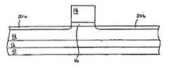
- FIG. 1 to FIG. 3show a series of schematic cross-sectional diagrams illustrating the results of progressive stages in fabricating a field effect transistor in accord with an embodiment of the invention.
- FIG. 1shows a semiconductor substrate 10 .
- a buried insulator layer 12is located upon the semiconductor substrate 10 and a semiconductor surface layer 14 is in turn located upon the buried insulator layer 12 .
- the buried insulator layer 12may be a crystalline or non-crystalline oxide or nitride.
- the substrate including layers 10 , 12 and 14is formed utilizing a conventional process such as, for example, SIMOX (separation by ion implantation of oxygen) or a layer transfer technique.
- the structure of the semiconductor substrate 10 , buried insulator layer 12 and semiconductor surface layer 14comprises a semiconductor-on-insulator semiconductor substrate that is typically a silicon semiconductor-on-insulator semiconductor substrate.
- the inventionis not, however, limited to a semiconductor structure formed within a silicon-on-insulator semiconductor substrate.
- the inventionalso includes semiconductor devices formed within bulk semiconductor substrates or SiGe-on-insulator substrates.
- the inventionmay in general be practiced employing silicon semiconductor substrates, silicon-germanium alloy semiconductor substrates and compound semiconductor substrates.
- the inventionmay be practiced with a bulk silicon semiconductor substrate, a semiconductor-on-insulator semiconductor substrate or a hybrid oriented technology semiconductor substrate that may have at least two surface regions of different crystallographic orientation.
- Typical crystalline orientations for the silicon semiconductor substrateare (100), (111) and (110).
- Hybrid substratesmay include one surface region having a first crystallographic orientation and a second surface region of a second crystallographic orientation that differs from the first crystallographic orientation.
- FIG. 1also shows a gate dielectric layer 16 located upon the semiconductor surface layer 14 and a gate electrode located upon at least a portion of the gate dielectric layer 16 .
- FIG. 1finally shows a pair of lightly doped extension regions 20 a and 20 b located within the semiconductor surface layer 14 and separated by a channel region within the semiconductor surface layer beneath the gate electrode 18 .
- the gate dielectric layer 16is typically comprised of an oxide, nitride, oxynitride or combination thereof formed to a thickness from about 10 to about 70 angstroms.
- an oxide having a dielectric constant, as measured in a vacuum, of about 4.0 or greateris employed as the gate dielectric 16 .
- the gate electrode 18is typically formed of a heavily doped (i.e., 1e20 to 1e21 dopant atoms per cubic centimeter) polysilicon material formed to a thickness from about 1000 to about 3000 angstroms.
- the gate electrodemay also comprise doped poly-SiGe, an elemental conductive metal, an alloy of an elemental conductive metal, a silicide of an elemental conductive metal, a nitride of an elemental conductive metal or any combination thereof, including combinations with doped poly-Si.
- the pair of lightly doped extension regions 20 a and 20 bis formed utilizing a comparatively low dose ion implantation method to provide a dopant of appropriate polarity at a concentration of from about 1e20 to about 5e20 dopant atoms per cubic centimeter.
- the pair of lightly doped extension regions 20 a and 20 bmay be optional in some embodiments of the invention.
- An optional halo ion implantmay also be used in some embodiments of the invention, although not specifically illustrated in FIG. 1 .
- FIG. 2shows a pair of spacers 22 a and 22 b located adjacent and adjoining the gate electrode 18 and the gate dielectric layer 16 .
- FIG. 2also shows a pair of source/drain regions 20 a ′ and 20 b ′ incorporating the pair of lightly doped extension regions 20 a and 20 b . They are also located in the semiconductor surface layer 14 . The pair of source/drain regions 20 a ′ and 20 b ′ continue to bound the channel region beneath the gate electrode 18 .
- the pair of spacers 22 a and 22 bis formed of a material that provides in part the subject matter of the invention. Materials constraints when forming the spacers 22 a and 22 b are disclosed in further detail below.
- the pair of source/drain regions 20 a and 20 bis formed with an appropriate dopant concentration and polarity while employing an additional ion implantation method.
- FIG. 3shows a series of silicide regions 24 a , 24 b and 24 c located upon the source/drain regions 20 a and 20 b and the gate electrode 18 .
- FIG. 3also shows an etch stop liner layer 26 that covers the field effect transistor.
- the series of silicide layers 24 a , 24 b and 24 cis formed utilizing a conventional self-aligned (i.e., salicidation) process to yield a silicide material formed to a thickness from about 50 to about 300 angstroms.
- the series of silicide layers 24 a , 24 b and 24 cassists in providing enhanced conductivity to the source/drain regions 20 a and 20 b and the gate electrode 18 .
- silicide materialsmay include, but are not limited to, titanium silicides, platinum silicides, nickel silicides, cobalt silicides, and other alloy combinations.
- a silicideis shown atop the gate electrode 18
- the present inventionalso contemplates embodiments in which the silicide is not located atop the gate electrode 18 .
- a dielectric capis present atop the gate electrode 18 during the salicidation process.
- the etch stop liner layer 26is typically formed of a silicon nitride material or other etch stop dielectric material formed to a thickness from about 300 to about 2000 angstroms.
- the intrinsic stress in this linercan be varied to be as high as 2 GPa for tensile applications on the NFET and ⁇ 3.5 to ⁇ 4 GPa for compressive applications for PFETs.
- FIG. 3finally shows crystallographic orientation reference axes for the field effect transistor.
- the inventionis directed towards the influence of materials properties of the pair of spacers 22 a and 22 b upon charge carrier mobility within the channel region beneath the gate electrode 18 .
- the inventionprovides that the pair of spacers 22 a and 22 b comprises a comparatively soft material having a modulus preferably from about 10 to about 50 GPa, more preferably from about 10 to about 25 GPa and most preferably from about 15 to about 20 GPa.
- a softnesslower modulus material being softer relative to higher modulus material
- the inventiondoes not specifically limit the type of materials that may be employed for forming the spacer having the modulus of from about 10 to about 50 GPa. From a practical point of view, any of several materials may be employed, including conductor materials, semiconductor materials and dielectric materials.
- a silicon oxide dielectric materialis desirable.
- An undoped silicon oxide dielectric material formed employing a plasma enhanced chemical vapor deposition methodis also desirable.
- Such a methodmay employ: (1) silane and nitrous oxide as silicon and oxygen source materials; (2) carrier gases such as nitrogen, helium or hydrogen; (3) a deposition pressure of less than 10 torr and more preferable less than 1 torr; (4) a deposition rate of from about 5 to about 25 angstroms per second and more preferably from about 10 to about 20 angstroms per second; and (5) a deposition temperature of from about 400° to about 480° C. and more preferably from about 430° to about 450° C.
- the inventionprovides spacers 22 a and 22 b with a particularly low etch rate in a hydrofluoric acid etchant.
- the etch ratemay be on the order of only about twice that of a thermal oxide etch rate and on the order of one fifth of other chemical vapor deposition deposited silicon oxide etch rates.
- a pre-salicidation hydrofluoric acid clean of a semiconductor structuremay be effected while minimally etching the pair of spacers 22 a and 22 b.
- FIG. 4shows a longitudinal stress topography graph for a field effect transistor not in accord with the invention.
- the field effect transistoris fabricated within a silicon-on-insulator (SOI) semiconductor substrate.
- SOIsilicon-on-insulator
- FIG. 4shows the buried oxide layer 12 .
- the silicon surface layer 14is located upon the buried oxide layer 12 .
- the gate electrode 18is located over the silicon surface layer 14 .
- the spacer 22 badjoins the gate electrode 18 .
- the etch stop liner layer 26is formed covering the gate electrode 18 , the spacer 22 b and exposed portions of the silicon surface layer 14 .
- the stress topography graph as illustrated in FIG. 4is calculated employing the following values for modulus for various components: (1) spacer 22 b is comprised of oxide and nitride materials which have moduli of 70 GPa and 350 GPa, respectively, and nitride etch stop liner layer 26 is assumed to have a modulus of 350 GPa (and the etch stop liner layer 26 is initially deposited with an intrinsic compressive stress of about ⁇ 2 GPa); (2) gate electrode 18 and the silicon surface layer 14 are assumed to have a modulus of 150 GPa; and (3) gate dielectric layer 16 (reference numeral omitted for clarity, but minimally shown as darkened line beneath gate 18 ) is assumed to have a modulus of 70 GPa.
- the compressive stress nitride etch stop liner 26is used over PFETs. The stress values are reversed when tensile nitride liners are used over the NFETs.
- FIG. 4shows a zero stress line 30 within the silicon surface layer 14 .
- To the right of the zero stress line 30is a single tensile stress topography line at 50 MPa tensile stress.
- To the left of the zero stress line 30is a series of three compressive stress lines increasing at ⁇ 50 MPa compressive stress intervals and terminating with ⁇ 150 MPa compressive stress beneath the gate electrode 18 .
- FIG. 5shows a stress topography graph corresponding with the stress topography graph of FIG. 4 , but with the exception that the calculation algorithm employs a modulus for the spacer 22 b of 20 GPa (within the range of the present invention) rather than a stack comprising materials of silicon oxide with modulus of 70 GPa and nitride with modulus of 350 GPa.
- reference numeral 30still corresponds with a zero stress line within the silicon surface layer 14 .
- To the right of reference numeral 30is a single tensile stress contour line at 50 MPa tensile stress.
- To the left of reference numeral 30is a series of five stress contour lines that end yielding ⁇ 250 MPa compressive stress within the channel region beneath the gate electrode 18 . Again this is for PFETs.
- FIG. 6 and FIG. 7show a pair of stress topography diagrams corresponding with the stress topography diagrams of FIG. 4 and FIG. 5 , but for stress in a vertical direction rather than a longitudinal direction.
- both FIG. 6 and FIG. 7illustrate a zero stress line 30 within the silicon surface layer 14 .
- To the left of the zero stress line 30are tensile stress contours and to the right of the zero stress line 30 are compressive stress contours.
- FIG. 6corresponds with FIG. 4 insofar as the spacer 22 b is formed of a material having an enhanced hardness and a stack with oxide with modulus of 70 GPa and silicon nitride with modulus of 350 GPa.
- FIG. 7corresponds with FIG. 5 insofar as the spacer 22 b is formed of a material having a decreased hardness and a modulus of 20 GPa.
- the semiconductor structure of FIG. 7has enhanced tensile vertical stress that may provide enhanced charge carrier mobility for a semiconductor substrate of certain crystallographic orientation and dopant polarity.
- FIG. 8 and FIG. 9summarize the stress information illustrated in the stress topography graphs of FIGS. 4-7 .
- reference numeral 61corresponds with a longitudinal stress profile for a field effect transistor fabricated with a 20 GPa modulus spacer.
- Reference numeral 62corresponds with a longitudinal stress profile for a field effect transistor fabricated with a spacer with a combined oxide/nitride stack with 70/350 GPa modulus.
- the low modulus spacerprovides greater compressive stress within a channel region that typically has a distance of about 0.02 microns from a mid-gate electrode dimension.
- reference numeral 71corresponds with a vertical stress profile for a field effect transistor fabricated with a 20 GPa modulus spacer.
- Reference numeral 72corresponds with a vertical stress profile for a field effect transistor fabricated with a spacer with a combined oxide nitride stack with 70/350 GPa modulus. As is seen in FIG. 9 , the channel region of the field effect transistor fabricated within the low modulus spacer has a higher tensile stress.
- Piezoresistance coefficients for (001) silicon in the order of longitudinal, transverse and vertical directions for n and p polaritiesare as follows (units are 1e-11/pascal): (1) for n silicon, ⁇ 31.6, ⁇ 17.6 and 53.4; (2) for p silicon, 71.8, ⁇ 1.1 and ⁇ 66.3. Piezoresistance coefficients for (110) p silicon are 71.8, ⁇ 66.3 and ⁇ 1.1.
- Crystallographic orientation (001) siliconis typically bulk silicon. Crystallographic orientation (110) silicon typically derives from a silicon-on-insulator semiconductor substrate.
- Charge carrier mobility enhancementsare typically calculated as a summary of piezoresistance coefficient times applied stress, and summed for each of the longitudinal, vertical and transverse directions.
- a longitudinal compressive stressis advantageous to a p-FET device whether fabricated on a (001) silicon semiconductor substrate or a (110) silicon semiconductor substrate.
- a vertical tensile stressis advantageous to a p-FET fabricated on a (110) silicon semiconductor substrate or an n-FET fabricated on a (001) silicon semiconductor substrate.
- n-FETis expected to have about a 16 percent charge carrier mobility enhancement and a p-FET is expected to have about a 20 percent charge carrier mobility enhancement.
- p-FET transistorshave added charge carrier mobility advantages when formed on (110) silicon surfaces in comparison with (001) silicon surfaces.
Landscapes
- Engineering & Computer Science (AREA)
- Physics & Mathematics (AREA)
- Microelectronics & Electronic Packaging (AREA)
- Condensed Matter Physics & Semiconductors (AREA)
- General Physics & Mathematics (AREA)
- Manufacturing & Machinery (AREA)
- Computer Hardware Design (AREA)
- Power Engineering (AREA)
- Chemical & Material Sciences (AREA)
- Chemical Kinetics & Catalysis (AREA)
- Plasma & Fusion (AREA)
- Insulated Gate Type Field-Effect Transistor (AREA)
- Thin Film Transistor (AREA)
Abstract
Description
- The invention relates generally to physical stress within semiconductor structures. More particularly, the invention relates to physical stress induced charge carrier mobility modification within semiconductor structures such as, for example, metal oxide semiconductor field effect transistors (MOSFETs).
- Recent advances in semiconductor device design and development have involved the introduction of applied physical stress into semiconductor device components. Applied physical stress often leads to charge carrier mobility modification. In particular, enhanced charge carrier mobility generally leads to enhanced semiconductor device performance.
- There are various examples of stress induced performance enhancement within semiconductor devices. For example, Doris et al., in U.S. Pat. No. 6,717,216 teaches a silicon-on-insulator field effect transistor device having a compressive stress in an undercut area to provide increased charge carrier mobility in the device. In addition, Chidambarrao et al., in U.S. Pat. No. 6,825,529 teaches that gate sidewall spacer material may affect tensile or compressive stress within a semiconductor channel region beneath a gate electrode.
- Other examples of compressive stress or tensile stress within various locations within semiconductor structures are alternatively known to provide charge carrier mobility modification. Typically, n-FET and p-FET devices respond differently to compressive and tensile stresses since piezoresistance coefficients will typically differ as a function of several variables, including, for instance, semiconductor substrate doping and crystallographic orientation. Thus, stressed components within n-FET and p-FET devices often need to be specifically engineered and optimized.
- A trend within semiconductor design and development is for continued enhanced performance at smaller dimensions. Thus, a need will continue to exist for novel structures and methods that form semiconductor devices such as MOSFETs having enhanced performance. To that end, the use of physically stressed structures in semiconductor technology is likely to continue. Desirable are alternative semiconductor structures and methods for fabrication that advantageously employ physical stress for semiconductor device performance enhancement.
- The present invention provides a semiconductor structure, such as, for example, a MOSFET, having enhanced performance.
- The invention also provides a method for readily manufacturing the semiconductor structure.
- In accord with the invention, the semiconductor structure comprises a semiconductor substrate having a gate electrode located atop (i.e., over) a surface of the semiconductor substrate and a channel region beneath the gate electrode within the semiconductor substrate. A spacer is formed adjacent to a sidewall of the gate electrode. The spacer is formed of a material having a modulus (Young's modulus) of from about 10 to about 50 gigapascals (GPa). Relative to normal spacer materials this modulus is much lower. This lower modulus spacer allows an enhanced transference of stress from the etch stop nitride liner to the channel. This enhancement is relative to an otherwise analogous structure where a spacer is made of plasma enhanced chemical vapor deposition (PECVD) or rapid thermal chemical vapor deposition (RTCVD) silicon nitride (with modulus typically about 350 GPa) or silicon oxide (with modulus typically about 70 GPa) formed using low temperature oxidation (LTO) or PECVD deposition.
- The invention is predicated upon the observation that a spacer having a modulus in the specified range provides enhanced stresses within certain semiconductor structures relative to analogous semiconductor structures having spacers formed of materials (as above) having moduli in a range greater than as taught in the invention (i.e., greater than 50 GPa). Enhanced longitudinal tensile stress and vertical compressive stress are obtained in a channel region of NFETs when tensile etch stop nitride liners are used in combination with low modulus spacers. Enhanced longitudinal compressive stress and vertical tensile stress are obtained in a channel region of PFETs when compressive etch stop nitride liners are used in combination with low modulus spacers. The enhanced stresses, in turn, provide for enhanced charge carrier mobility. The invention is particularly applicable to field effect transistors including n-FETs, p-FETS and a combination thereof.
- The invention also provides a comparatively low modulus spacer comprised of a particular silicon oxide material formed utilizing a particular plasma enhanced chemical vapor deposition method. A spacer formed employing the inventive method has a particularly low etch rate when a hydrofluoric acid etchant is employed in fabricating a field effect transistor.
FIG. 1 ,FIG. 2 andFIG. 3 show a series of schematic cross-sectional diagrams illustrating the results of progressive stages in fabricating a field effect transistor in accord with the invention.FIG. 4 andFIG. 5 show a pair of lateral stress topography graphs for a field effect transistor fabricated not in accord with the invention, and fabricated in accord with the invention.FIG. 6 andFIG. 7 show a pair of vertical stress topography graphs for a field effect transistor fabricated not in accord with the invention, and fabricated in accord with the invention.FIG. 8 andFIG. 9 show a pair lateral stress and vertical stress graphs that summarize the stress topography graphs ofFIG. 4 toFIG. 7 .- The invention provides a semiconductor structure and a method for fabricating the semiconductor structure. The semiconductor structure may be fabricated with enhanced performance with respect to charge carrier mobility. The invention realizes the foregoing result by employing a spacer formed adjacent a gate electrode sidewall within the semiconductor structure with a modulus within a specific range. The modulus range is generally low. By “low” it is meant less than about 50 GPa and preferably from about 10 to about 50 GPa. The sidewall spacer having a low modulus provides for enhanced lateral compressive stress and enhanced vertical tensile stress within a channel beneath the gate electrode when used in tandem with highly stressed etch stop nitride liners. When mated with an appropriate semiconductor substrate crystallographic orientation, the spacer assists in providing enhanced charge carrier mobility within the semiconductor structure.
- Although the invention is preferably applicable to field effect transistors, the invention is not intended to be so limited. The invention is applicable to any of several semiconductor devices that may employ a gate type electrode or related structure over a channel region within a semiconductor substrate, where the gate has a spacer formed adjacent thereto.
FIG. 1 toFIG. 3 show a series of schematic cross-sectional diagrams illustrating the results of progressive stages in fabricating a field effect transistor in accord with an embodiment of the invention.FIG. 1 shows asemiconductor substrate 10. A buriedinsulator layer 12 is located upon thesemiconductor substrate 10 and asemiconductor surface layer 14 is in turn located upon the buriedinsulator layer 12. The buriedinsulator layer 12 may be a crystalline or non-crystalline oxide or nitride. Thesubstrate including layers - The structure of the
semiconductor substrate 10, buriedinsulator layer 12 andsemiconductor surface layer 14 comprises a semiconductor-on-insulator semiconductor substrate that is typically a silicon semiconductor-on-insulator semiconductor substrate. The invention is not, however, limited to a semiconductor structure formed within a silicon-on-insulator semiconductor substrate. The invention also includes semiconductor devices formed within bulk semiconductor substrates or SiGe-on-insulator substrates. The invention may in general be practiced employing silicon semiconductor substrates, silicon-germanium alloy semiconductor substrates and compound semiconductor substrates. - The invention may be practiced with a bulk silicon semiconductor substrate, a semiconductor-on-insulator semiconductor substrate or a hybrid oriented technology semiconductor substrate that may have at least two surface regions of different crystallographic orientation. Typical crystalline orientations for the silicon semiconductor substrate are (100), (111) and (110). Hybrid substrates may include one surface region having a first crystallographic orientation and a second surface region of a second crystallographic orientation that differs from the first crystallographic orientation.
FIG. 1 also shows a gatedielectric layer 16 located upon thesemiconductor surface layer 14 and a gate electrode located upon at least a portion of the gatedielectric layer 16.FIG. 1 finally shows a pair of lightly dopedextension regions 20aand20blocated within thesemiconductor surface layer 14 and separated by a channel region within the semiconductor surface layer beneath thegate electrode 18.- The gate
dielectric layer 16 is typically comprised of an oxide, nitride, oxynitride or combination thereof formed to a thickness from about 10 to about 70 angstroms. Preferably, an oxide having a dielectric constant, as measured in a vacuum, of about 4.0 or greater is employed as thegate dielectric 16. Thegate electrode 18 is typically formed of a heavily doped (i.e., 1e20 to 1e21 dopant atoms per cubic centimeter) polysilicon material formed to a thickness from about 1000 to about 3000 angstroms. In addition to doped polysilicon, the gate electrode may also comprise doped poly-SiGe, an elemental conductive metal, an alloy of an elemental conductive metal, a silicide of an elemental conductive metal, a nitride of an elemental conductive metal or any combination thereof, including combinations with doped poly-Si. - The pair of lightly doped
extension regions 20aand20bis formed utilizing a comparatively low dose ion implantation method to provide a dopant of appropriate polarity at a concentration of from about 1e20 to about 5e20 dopant atoms per cubic centimeter. The pair of lightly dopedextension regions 20aand20bmay be optional in some embodiments of the invention. An optional halo ion implant may also be used in some embodiments of the invention, although not specifically illustrated inFIG. 1 . FIG. 2 shows a pair ofspacers 22aand22blocated adjacent and adjoining thegate electrode 18 and thegate dielectric layer 16.FIG. 2 also shows a pair of source/drain regions 20a′ and20b′ incorporating the pair of lightly dopedextension regions 20aand20b. They are also located in thesemiconductor surface layer 14. The pair of source/drain regions 20a′ and20b′ continue to bound the channel region beneath thegate electrode 18.- The pair of
spacers 22aand22bis formed of a material that provides in part the subject matter of the invention. Materials constraints when forming thespacers 22aand22bare disclosed in further detail below. - The pair of source/
drain regions 20aand20bis formed with an appropriate dopant concentration and polarity while employing an additional ion implantation method. FIG. 3 shows a series ofsilicide regions 24a,24band24clocated upon the source/drain regions 20aand20band thegate electrode 18.FIG. 3 also shows an etchstop liner layer 26 that covers the field effect transistor.- The series of
silicide layers 24a,24band24cis formed utilizing a conventional self-aligned (i.e., salicidation) process to yield a silicide material formed to a thickness from about 50 to about 300 angstroms. The series ofsilicide layers 24a,24band24cassists in providing enhanced conductivity to the source/drain regions 20aand20band thegate electrode 18. Typically, such silicide materials may include, but are not limited to, titanium silicides, platinum silicides, nickel silicides, cobalt silicides, and other alloy combinations. - Although a silicide is shown atop the
gate electrode 18, the present invention also contemplates embodiments in which the silicide is not located atop thegate electrode 18. In such embodiments, a dielectric cap is present atop thegate electrode 18 during the salicidation process. - Finally, the etch
stop liner layer 26 is typically formed of a silicon nitride material or other etch stop dielectric material formed to a thickness from about 300 to about 2000 angstroms. The intrinsic stress in this liner can be varied to be as high as 2 GPa for tensile applications on the NFET and −3.5 to −4 GPa for compressive applications for PFETs. FIG. 3 finally shows crystallographic orientation reference axes for the field effect transistor. When formed utilizing a (001) oriented substrate, crystallographic orientation planes are L=(110), T=(1-10) and V=(001). When formed utilizing a (110) oriented substrate, crystallographic orientation planes are L=(110), T=(001) and V=(1-10).- The invention is directed towards the influence of materials properties of the pair of
spacers 22aand22bupon charge carrier mobility within the channel region beneath thegate electrode 18. To that end, the invention provides that the pair ofspacers 22aand22bcomprises a comparatively soft material having a modulus preferably from about 10 to about 50 GPa, more preferably from about 10 to about 25 GPa and most preferably from about 15 to about 20 GPa. As will be shown in the series of stress topography graphs that follows, a softness (lower modulus material being softer relative to higher modulus material) in the foregoing ranges provides for enhanced charge carrier mobility performance of a field effect transistor when fabricated upon a particular silicon semiconductor substrate crystallographic orientation. - The invention does not specifically limit the type of materials that may be employed for forming the spacer having the modulus of from about 10 to about 50 GPa. From a practical point of view, any of several materials may be employed, including conductor materials, semiconductor materials and dielectric materials. A silicon oxide dielectric material is desirable. An undoped silicon oxide dielectric material formed employing a plasma enhanced chemical vapor deposition method is also desirable. Such a method may employ: (1) silane and nitrous oxide as silicon and oxygen source materials; (2) carrier gases such as nitrogen, helium or hydrogen; (3) a deposition pressure of less than 10 torr and more preferable less than 1 torr; (4) a deposition rate of from about 5 to about 25 angstroms per second and more preferably from about 10 to about 20 angstroms per second; and (5) a deposition temperature of from about 400° to about 480° C. and more preferably from about 430° to about 450° C.
- The foregoing limitations are desirable for forming the undoped silicon oxide material from which is formed the
spacers 22aand22b. When employing those limitations, the invention providesspacers 22aand22bwith a particularly low etch rate in a hydrofluoric acid etchant. The etch rate may be on the order of only about twice that of a thermal oxide etch rate and on the order of one fifth of other chemical vapor deposition deposited silicon oxide etch rates. Under these circumstances, a pre-salicidation hydrofluoric acid clean of a semiconductor structure may be effected while minimally etching the pair ofspacers 22aand22b. FIG. 4 shows a longitudinal stress topography graph for a field effect transistor not in accord with the invention. The field effect transistor is fabricated within a silicon-on-insulator (SOI) semiconductor substrate.FIG. 4 shows the buriedoxide layer 12. Thesilicon surface layer 14 is located upon the buriedoxide layer 12. Thegate electrode 18 is located over thesilicon surface layer 14. The spacer22badjoins thegate electrode 18. Finally, the etchstop liner layer 26 is formed covering thegate electrode 18, the spacer22band exposed portions of thesilicon surface layer 14.- The stress topography graph as illustrated in
FIG. 4 is calculated employing the following values for modulus for various components: (1) spacer22bis comprised of oxide and nitride materials which have moduli of 70 GPa and 350 GPa, respectively, and nitride etchstop liner layer 26 is assumed to have a modulus of 350 GPa (and the etchstop liner layer 26 is initially deposited with an intrinsic compressive stress of about −2 GPa); (2)gate electrode 18 and thesilicon surface layer 14 are assumed to have a modulus of 150 GPa; and (3) gate dielectric layer16 (reference numeral omitted for clarity, but minimally shown as darkened line beneath gate18) is assumed to have a modulus of 70 GPa. The compressive stress nitrideetch stop liner 26 is used over PFETs. The stress values are reversed when tensile nitride liners are used over the NFETs. FIG. 4 shows a zerostress line 30 within thesilicon surface layer 14. To the right of the zerostress line 30 is a single tensile stress topography line at 50 MPa tensile stress. To the left of the zerostress line 30 is a series of three compressive stress lines increasing at −50 MPa compressive stress intervals and terminating with −150 MPa compressive stress beneath thegate electrode 18.FIG. 5 shows a stress topography graph corresponding with the stress topography graph ofFIG. 4 , but with the exception that the calculation algorithm employs a modulus for the spacer22bof 20 GPa (within the range of the present invention) rather than a stack comprising materials of silicon oxide with modulus of 70 GPa and nitride with modulus of 350 GPa. As illustrated inFIG. 5 ,reference numeral 30 still corresponds with a zero stress line within thesilicon surface layer 14. To the right ofreference numeral 30 is a single tensile stress contour line at 50 MPa tensile stress. To the left ofreference numeral 30 is a series of five stress contour lines that end yielding −250 MPa compressive stress within the channel region beneath thegate electrode 18. Again this is for PFETs.- Thus, as is seen by the comparison of
FIG. 4 andFIG. 5 , the use of a spacer of a generally lower modulus of about 20 GPa in comparison with a higher modulus stack of oxide with modulus of 70 GPa and a nitride of about 350 GPa yields higher compressive stresses in a longitudinal direction in a channel region of a field effect transistor. FIG. 6 andFIG. 7 show a pair of stress topography diagrams corresponding with the stress topography diagrams ofFIG. 4 andFIG. 5 , but for stress in a vertical direction rather than a longitudinal direction. Similarly withFIG. 4 andFIG. 5 , bothFIG. 6 andFIG. 7 illustrate a zerostress line 30 within thesilicon surface layer 14. To the left of the zerostress line 30 are tensile stress contours and to the right of the zerostress line 30 are compressive stress contours.FIG. 6 corresponds withFIG. 4 insofar as the spacer22bis formed of a material having an enhanced hardness and a stack with oxide with modulus of 70 GPa and silicon nitride with modulus of 350 GPa.FIG. 7 corresponds withFIG. 5 insofar as the spacer22bis formed of a material having a decreased hardness and a modulus of 20 GPa.- As seen from comparison of
FIG. 6 andFIG. 7 , there is an additional tensile stress contour line within the channel region beneath thegate electrode 18 withinFIG. 7 having the comparatively soft spacer22bof modulus about 20 GPa. Thus, the semiconductor structure ofFIG. 7 has enhanced tensile vertical stress that may provide enhanced charge carrier mobility for a semiconductor substrate of certain crystallographic orientation and dopant polarity. FIG. 8 andFIG. 9 summarize the stress information illustrated in the stress topography graphs ofFIGS. 4-7 .- Within
FIG. 8 reference numeral61 corresponds with a longitudinal stress profile for a field effect transistor fabricated with a 20 GPa modulus spacer.Reference numeral 62 corresponds with a longitudinal stress profile for a field effect transistor fabricated with a spacer with a combined oxide/nitride stack with 70/350 GPa modulus. As is seen inFIG. 8 , the low modulus spacer provides greater compressive stress within a channel region that typically has a distance of about 0.02 microns from a mid-gate electrode dimension. - Within
FIG. 9 , reference numeral71 corresponds with a vertical stress profile for a field effect transistor fabricated with a 20 GPa modulus spacer.Reference numeral 72 corresponds with a vertical stress profile for a field effect transistor fabricated with a spacer with a combined oxide nitride stack with 70/350 GPa modulus. As is seen inFIG. 9 , the channel region of the field effect transistor fabricated within the low modulus spacer has a higher tensile stress. - Piezoresistance coefficients for (001) silicon in the order of longitudinal, transverse and vertical directions for n and p polarities are as follows (units are 1e-11/pascal): (1) for n silicon, −31.6, −17.6 and 53.4; (2) for p silicon, 71.8, −1.1 and −66.3. Piezoresistance coefficients for (110) p silicon are 71.8, −66.3 and −1.1. Crystallographic orientation (001) silicon is typically bulk silicon. Crystallographic orientation (110) silicon typically derives from a silicon-on-insulator semiconductor substrate. Charge carrier mobility enhancements are typically calculated as a summary of piezoresistance coefficient times applied stress, and summed for each of the longitudinal, vertical and transverse directions.
- As a consequence of dimensionally appropriate enhanced stress within channel regions, the invention provides an opportunity for charge carrier mobility improvement within both n-FET and p-FET devices. A longitudinal compressive stress is advantageous to a p-FET device whether fabricated on a (001) silicon semiconductor substrate or a (110) silicon semiconductor substrate. A vertical tensile stress is advantageous to a p-FET fabricated on a (110) silicon semiconductor substrate or an n-FET fabricated on a (001) silicon semiconductor substrate.
- There are several calculation algorithms that may be employed to approximate charge carrier mobility gains for field effect transistors in accord with an embodiment of the invention. As an approximate summary with respect to low modulus spacers in comparison with high modulus spacers, an n-FET is expected to have about a 16 percent charge carrier mobility enhancement and a p-FET is expected to have about a 20 percent charge carrier mobility enhancement. In addition, p-FET transistors have added charge carrier mobility advantages when formed on (110) silicon surfaces in comparison with (001) silicon surfaces.
- The preferred embodiment of the invention is illustrative of the invention rather than limiting of the invention. Revisions and modifications may be made to methods, materials, structures and dimensions in accord with the preferred embodiment of the invention while still providing an embodiment in accord with the invention, further in accord with the accompanying claims.
Claims (18)
1. A semiconductor structure comprising:
a semiconductor substrate comprising a channel region;
a gate electrode located over the semiconductor substrate atop the channel region; and
a spacer adjacent to a sidewall of the gate electrode, where the spacer is formed of a material having a modulus from about 10 to about 50 GPa.
2. The structure ofclaim 1 wherein the spacer is comprised of a dielectric material.
3. The structure ofclaim 1 wherein the spacer is comprised of a conductor material.
4. The structure ofclaim 1 wherein the gate electrode is a component of a field effect transistor.
5. The structure ofclaim 1 wherein the spacer is comprised of a material having a modulus from about 10 to about 25 GPa.
6. The device ofclaim 1 wherein the spacer is comprised of a material having a modulus from about 15 to about 20 GPa.
7. A method for fabricating a semiconductor structure comprising:
forming a gate electrode over a semiconductor substrate, the semiconductor substrate including a channel region; and
forming a spacer adjacent to a sidewall of the gate electrode, where the spacer is formed of a material having a modulus from about 10 to about 50 GPa.
8. The method ofclaim 7 wherein the spacer is comprised of a dielectric material.
9. The method ofclaim 7 wherein the gate electrode is a component of a field effect transistor.
10. The method ofclaim 7 wherein the spacer is comprised of a material having a modulus of from about 10 to about 25 GPa.
11. The method ofclaim 7 wherein the spacer is comprised of a material having a modulus from about 15 to about 20 GPa.
12. A method for fabricating a semiconductor structure comprising:
forming a gate electrode over a semiconductor substrate, the semiconductor substrate having a channel region; and
forming a spacer adjacent to a sidewall of the gate electrode, where the spacer is formed of a silicon oxide material having a modulus from about 10 to about 50 GPa.
13. The method ofclaim 12 wherein the silicon oxide material is formed employing a plasma enhanced chemical vapor deposition method.
14. The method ofclaim 13 wherein the plasma enhanced chemical vapor deposition method employs silane as a silicon source material and nitrous oxide as an oxidant source material.
15. The method ofclaim 13 wherein the plasma enhanced chemical vapor deposition method employs a deposition temperature from about 400° to about 480° C.
16. The method ofclaim 13 wherein the plasma enhanced chemical vapor deposition method employs a deposition rate from about 5 to about 25 angstroms per second.
17. The method ofclaim 12 wherein the silicon oxide material has a modulus from about 10 to about 25 GPa.
18. The method ofclaim 12 wherein the silicon oxide material has a modulus from about 15 to about 20 GPa.
Priority Applications (3)
| Application Number | Priority Date | Filing Date | Title |
|---|---|---|---|
| US11/163,871US20070096170A1 (en) | 2005-11-02 | 2005-11-02 | Low modulus spacers for channel stress enhancement |
| JP2006294911AJP2007129223A (en) | 2005-11-02 | 2006-10-30 | Semiconductor structure and fabrication method (low Young's modulus spacer to improve channel stress) |
| CNA2006101432737ACN1960004A (en) | 2005-11-02 | 2006-11-01 | Semiconductor structure and manufacturing method thereof |
Applications Claiming Priority (1)
| Application Number | Priority Date | Filing Date | Title |
|---|---|---|---|
| US11/163,871US20070096170A1 (en) | 2005-11-02 | 2005-11-02 | Low modulus spacers for channel stress enhancement |
Publications (1)
| Publication Number | Publication Date |
|---|---|
| US20070096170A1true US20070096170A1 (en) | 2007-05-03 |
Family
ID=37995109
Family Applications (1)
| Application Number | Title | Priority Date | Filing Date |
|---|---|---|---|
| US11/163,871AbandonedUS20070096170A1 (en) | 2005-11-02 | 2005-11-02 | Low modulus spacers for channel stress enhancement |
Country Status (3)
| Country | Link |
|---|---|
| US (1) | US20070096170A1 (en) |
| JP (1) | JP2007129223A (en) |
| CN (1) | CN1960004A (en) |
Cited By (13)
| Publication number | Priority date | Publication date | Assignee | Title |
|---|---|---|---|---|
| US20070155073A1 (en)* | 2006-01-03 | 2007-07-05 | Freescale Semiconductor, Inc. | Method of forming device having a raised extension region |
| US20080029832A1 (en)* | 2006-08-03 | 2008-02-07 | Micron Technology, Inc. | Bonded strained semiconductor with a desired surface orientation and conductance direction |
| US20080272395A1 (en)* | 2007-05-03 | 2008-11-06 | Dsm Solutions, Inc. | Enhanced hole mobility p-type jfet and fabrication method therefor |
| US20090085097A1 (en)* | 2007-09-27 | 2009-04-02 | Lucian Shifren | Methods of forming nitride stressing layer for replacement metal gate and structures formed thereby |
| US20090108363A1 (en)* | 2006-08-02 | 2009-04-30 | Leonard Forbes | Strained semiconductor, devices and systems and methods of formation |
| US20090218566A1 (en)* | 2006-02-16 | 2009-09-03 | Micron Technology, Inc. | Localized compressive strained semiconductor |
| US20090288048A1 (en)* | 2005-12-01 | 2009-11-19 | Synopsys, Inc. | Analysis of stress impact on transistor performance |
| US20130134523A1 (en)* | 2011-01-25 | 2013-05-30 | International Business Machines Corporation | Cmos transistors having differentially stressed spacers |
| US8847324B2 (en) | 2012-12-17 | 2014-09-30 | Synopsys, Inc. | Increasing ION /IOFF ratio in FinFETs and nano-wires |
| US9177894B2 (en) | 2012-08-31 | 2015-11-03 | Synopsys, Inc. | Latch-up suppression and substrate noise coupling reduction through a substrate back-tie for 3D integrated circuits |
| US9379018B2 (en) | 2012-12-17 | 2016-06-28 | Synopsys, Inc. | Increasing Ion/Ioff ratio in FinFETs and nano-wires |
| US9379241B2 (en) | 2006-08-18 | 2016-06-28 | Micron Technology, Inc. | Semiconductor device with strained channels |
| US9817928B2 (en) | 2012-08-31 | 2017-11-14 | Synopsys, Inc. | Latch-up suppression and substrate noise coupling reduction through a substrate back-tie for 3D integrated circuits |
Families Citing this family (1)
| Publication number | Priority date | Publication date | Assignee | Title |
|---|---|---|---|---|
| US8530886B2 (en)* | 2011-03-18 | 2013-09-10 | International Business Machines Corporation | Nitride gate dielectric for graphene MOSFET |
Citations (86)
| Publication number | Priority date | Publication date | Assignee | Title |
|---|---|---|---|---|
| US3602841A (en)* | 1970-06-18 | 1971-08-31 | Ibm | High frequency bulk semiconductor amplifiers and oscillators |
| US4665415A (en)* | 1985-04-24 | 1987-05-12 | International Business Machines Corporation | Semiconductor device with hole conduction via strained lattice |
| US4853076A (en)* | 1983-12-29 | 1989-08-01 | Massachusetts Institute Of Technology | Semiconductor thin films |
| US4855245A (en)* | 1985-09-13 | 1989-08-08 | Siemens Aktiengesellschaft | Method of manufacturing integrated circuit containing bipolar and complementary MOS transistors on a common substrate |
| US4952524A (en)* | 1989-05-05 | 1990-08-28 | At&T Bell Laboratories | Semiconductor device manufacture including trench formation |
| US4958213A (en)* | 1987-12-07 | 1990-09-18 | Texas Instruments Incorporated | Method for forming a transistor base region under thick oxide |
| US5006913A (en)* | 1988-11-05 | 1991-04-09 | Mitsubishi Denki Kabushiki Kaisha | Stacked type semiconductor device |
| US5060030A (en)* | 1990-07-18 | 1991-10-22 | Raytheon Company | Pseudomorphic HEMT having strained compensation layer |
| US5081513A (en)* | 1991-02-28 | 1992-01-14 | Xerox Corporation | Electronic device with recovery layer proximate to active layer |
| US5108843A (en)* | 1988-11-30 | 1992-04-28 | Ricoh Company, Ltd. | Thin film semiconductor and process for producing the same |
| US5134085A (en)* | 1991-11-21 | 1992-07-28 | Micron Technology, Inc. | Reduced-mask, split-polysilicon CMOS process, incorporating stacked-capacitor cells, for fabricating multi-megabit dynamic random access memories |
| US5310446A (en)* | 1990-01-10 | 1994-05-10 | Ricoh Company, Ltd. | Method for producing semiconductor film |
| US5354695A (en)* | 1992-04-08 | 1994-10-11 | Leedy Glenn J | Membrane dielectric isolation IC fabrication |
| US5371399A (en)* | 1991-06-14 | 1994-12-06 | International Business Machines Corporation | Compound semiconductor having metallic inclusions and devices fabricated therefrom |
| US5391510A (en)* | 1992-02-28 | 1995-02-21 | International Business Machines Corporation | Formation of self-aligned metal gate FETs using a benignant removable gate material during high temperature steps |
| US5459346A (en)* | 1988-06-28 | 1995-10-17 | Ricoh Co., Ltd. | Semiconductor substrate with electrical contact in groove |
| US5557122A (en)* | 1995-05-12 | 1996-09-17 | Alliance Semiconductors Corporation | Semiconductor electrode having improved grain structure and oxide growth properties |
| US5561302A (en)* | 1994-09-26 | 1996-10-01 | Motorola, Inc. | Enhanced mobility MOSFET device and method |
| US5670798A (en)* | 1995-03-29 | 1997-09-23 | North Carolina State University | Integrated heterostructures of Group III-V nitride semiconductor materials including epitaxial ohmic contact non-nitride buffer layer and methods of fabricating same |
| US5679965A (en)* | 1995-03-29 | 1997-10-21 | North Carolina State University | Integrated heterostructures of Group III-V nitride semiconductor materials including epitaxial ohmic contact, non-nitride buffer layer and methods of fabricating same |
| US5861651A (en)* | 1997-02-28 | 1999-01-19 | Lucent Technologies Inc. | Field effect devices and capacitors with improved thin film dielectrics and method for making same |
| US5880040A (en)* | 1996-04-15 | 1999-03-09 | Macronix International Co., Ltd. | Gate dielectric based on oxynitride grown in N2 O and annealed in NO |
| US5940736A (en)* | 1997-03-11 | 1999-08-17 | Lucent Technologies Inc. | Method for forming a high quality ultrathin gate oxide layer |
| US5960297A (en)* | 1997-07-02 | 1999-09-28 | Kabushiki Kaisha Toshiba | Shallow trench isolation structure and method of forming the same |
| US5966606A (en)* | 1996-05-20 | 1999-10-12 | Nec Corporation | Method for manufacturing a MOSFET having a side-wall film formed through nitridation of the gate electrode |
| US5989978A (en)* | 1998-07-16 | 1999-11-23 | Chartered Semiconductor Manufacturing, Ltd. | Shallow trench isolation of MOSFETS with reduced corner parasitic currents |
| US6008126A (en)* | 1992-04-08 | 1999-12-28 | Elm Technology Corporation | Membrane dielectric isolation IC fabrication |
| US6025280A (en)* | 1997-04-28 | 2000-02-15 | Lucent Technologies Inc. | Use of SiD4 for deposition of ultra thin and controllable oxides |
| US6066545A (en)* | 1997-12-09 | 2000-05-23 | Texas Instruments Incorporated | Birdsbeak encroachment using combination of wet and dry etch for isolation nitride |
| US6090684A (en)* | 1998-07-31 | 2000-07-18 | Hitachi, Ltd. | Method for manufacturing semiconductor device |
| US6107143A (en)* | 1998-03-02 | 2000-08-22 | Samsung Electronics Co., Ltd. | Method for forming a trench isolation structure in an integrated circuit |
| US6117722A (en)* | 1999-02-18 | 2000-09-12 | Taiwan Semiconductor Manufacturing Company | SRAM layout for relaxing mechanical stress in shallow trench isolation technology and method of manufacture thereof |
| US6133071A (en)* | 1997-10-15 | 2000-10-17 | Nec Corporation | Semiconductor device with plate heat sink free from cracks due to thermal stress and process for assembling it with package |
| US6165383A (en)* | 1998-04-10 | 2000-12-26 | Organic Display Technology | Useful precursors for organic electroluminescent materials and devices made from such materials |
| US6221735B1 (en)* | 2000-02-15 | 2001-04-24 | Philips Semiconductors, Inc. | Method for eliminating stress induced dislocations in CMOS devices |
| US6228694B1 (en)* | 1999-06-28 | 2001-05-08 | Intel Corporation | Method of increasing the mobility of MOS transistors by use of localized stress regions |
| US6235654B1 (en)* | 2000-07-25 | 2001-05-22 | Advanced Micro Devices, Inc. | Process for forming PECVD nitride with a very low deposition rate |
| US6255169B1 (en)* | 1999-02-22 | 2001-07-03 | Advanced Micro Devices, Inc. | Process for fabricating a high-endurance non-volatile memory device |
| US6261964B1 (en)* | 1997-03-14 | 2001-07-17 | Micron Technology, Inc. | Material removal method for forming a structure |
| US6265317B1 (en)* | 2001-01-09 | 2001-07-24 | Taiwan Semiconductor Manufacturing Company | Top corner rounding for shallow trench isolation |
| US20010009784A1 (en)* | 1998-01-09 | 2001-07-26 | Yanjun Ma | Structure and method of making a sub-micron MOS transistor |
| US6274444B1 (en)* | 1999-07-30 | 2001-08-14 | United Microelectronics Corp. | Method for forming mosfet |
| US6281532B1 (en)* | 1999-06-28 | 2001-08-28 | Intel Corporation | Technique to obtain increased channel mobilities in NMOS transistors by gate electrode engineering |
| US6284626B1 (en)* | 1999-04-06 | 2001-09-04 | Vantis Corporation | Angled nitrogen ion implantation for minimizing mechanical stress on side walls of an isolation trench |
| US6284623B1 (en)* | 1999-10-25 | 2001-09-04 | Peng-Fei Zhang | Method of fabricating semiconductor devices using shallow trench isolation with reduced narrow channel effect |
| US6319794B1 (en)* | 1998-10-14 | 2001-11-20 | International Business Machines Corporation | Structure and method for producing low leakage isolation devices |
| US20010044220A1 (en)* | 2000-01-18 | 2001-11-22 | Sey-Ping Sun | Method Of Forming Silicon Oxynitride Films |
| US6326667B1 (en)* | 1999-09-09 | 2001-12-04 | Kabushiki Kaisha Toshiba | Semiconductor devices and methods for producing semiconductor devices |
| US20010051426A1 (en)* | 1999-11-22 | 2001-12-13 | Scott K. Pozder | Method for forming a semiconductor device having a mechanically robust pad interface. |
| US6362082B1 (en)* | 1999-06-28 | 2002-03-26 | Intel Corporation | Methodology for control of short channel effects in MOS transistors |
| US6361885B1 (en)* | 1998-04-10 | 2002-03-26 | Organic Display Technology | Organic electroluminescent materials and device made from such materials |
| US6368931B1 (en)* | 2000-03-27 | 2002-04-09 | Intel Corporation | Thin tensile layers in shallow trench isolation and method of making same |
| US6403486B1 (en)* | 2001-04-30 | 2002-06-11 | Taiwan Semiconductor Manufacturing Company | Method for forming a shallow trench isolation |
| US6403975B1 (en)* | 1996-04-09 | 2002-06-11 | Max-Planck Gesellschaft Zur Forderung Der Wissenschafteneev | Semiconductor components, in particular photodetectors, light emitting diodes, optical modulators and waveguides with multilayer structures grown on silicon substrates |
| US6406973B1 (en)* | 1999-06-29 | 2002-06-18 | Hyundai Electronics Industries Co., Ltd. | Transistor in a semiconductor device and method of manufacturing the same |
| US20020074589A1 (en)* | 2000-11-28 | 2002-06-20 | Kamel Benaissa | Semiconductor varactor with reduced parasitic resistance |
| US20020081794A1 (en)* | 2000-12-26 | 2002-06-27 | Nec Corporation | Enhanced deposition control in fabricating devices in a semiconductor wafer |
| US20020086472A1 (en)* | 2000-12-29 | 2002-07-04 | Brian Roberds | Technique to obtain high mobility channels in MOS transistors by forming a strain layer on an underside of a channel |
| US20020086497A1 (en)* | 2000-12-30 | 2002-07-04 | Kwok Siang Ping | Beaker shape trench with nitride pull-back for STI |
| US6417046B1 (en)* | 2000-05-05 | 2002-07-09 | Taiwan Semiconductor Manufacturing Company | Modified nitride spacer for solving charge retention issue in floating gate memory cell |
| US20020090791A1 (en)* | 1999-06-28 | 2002-07-11 | Brian S. Doyle | Method for reduced capacitance interconnect system using gaseous implants into the ild |
| US6461936B1 (en)* | 2002-01-04 | 2002-10-08 | Infineon Technologies Ag | Double pullback method of filling an isolation trench |
| US6476462B2 (en)* | 1999-12-28 | 2002-11-05 | Texas Instruments Incorporated | MOS-type semiconductor device and method for making same |
| US6493497B1 (en)* | 2000-09-26 | 2002-12-10 | Motorola, Inc. | Electro-optic structure and process for fabricating same |
| US6498358B1 (en)* | 2001-07-20 | 2002-12-24 | Motorola, Inc. | Structure and method for fabricating an electro-optic system having an electrochromic diffraction grating |
| US6501121B1 (en)* | 2000-11-15 | 2002-12-31 | Motorola, Inc. | Semiconductor structure |
| US6506652B2 (en)* | 1998-11-13 | 2003-01-14 | Intel Corporation | Method of recessing spacers to improved salicide resistance on polysilicon gates |
| US20030032261A1 (en)* | 2001-08-08 | 2003-02-13 | Ling-Yen Yeh | Method of preventing threshold voltage of MOS transistor from being decreased by shallow trench isolation formation |
| US20030040158A1 (en)* | 2001-08-21 | 2003-02-27 | Nec Corporation | Semiconductor device and method of fabricating the same |
| US6531369B1 (en)* | 2000-03-01 | 2003-03-11 | Applied Micro Circuits Corporation | Heterojunction bipolar transistor (HBT) fabrication using a selectively deposited silicon germanium (SiGe) |
| US6531740B2 (en)* | 2001-07-17 | 2003-03-11 | Motorola, Inc. | Integrated impedance matching and stability network |
| US20030057184A1 (en)* | 2001-09-22 | 2003-03-27 | Shiuh-Sheng Yu | Method for pull back SiN to increase rounding effect in a shallow trench isolation process |
| US20030067035A1 (en)* | 2001-09-28 | 2003-04-10 | Helmut Tews | Gate processing method with reduced gate oxide corner and edge thinning |
| US6603156B2 (en)* | 2001-03-31 | 2003-08-05 | International Business Machines Corporation | Strained silicon on insulator structures |
| US6717716B2 (en)* | 2001-02-15 | 2004-04-06 | Seiko Epson Corporation | Method of manufacturing electrophoretic device and method of manufacturing electronic apparatus |
| US20040113217A1 (en)* | 2002-12-12 | 2004-06-17 | International Business Machines Corporation | Stress inducing spacers |
| US6767802B1 (en)* | 2003-09-19 | 2004-07-27 | Sharp Laboratories Of America, Inc. | Methods of making relaxed silicon-germanium on insulator via layer transfer |
| US6774015B1 (en)* | 2002-12-19 | 2004-08-10 | International Business Machines Corporation | Strained silicon-on-insulator (SSOI) and method to form the same |
| US6784094B2 (en)* | 1998-09-03 | 2004-08-31 | Micron Technology, Inc. | Anti-reflective coatings and methods for forming and using same |
| US6809043B1 (en)* | 2002-06-19 | 2004-10-26 | Advanced Micro Devices, Inc. | Multi-stage, low deposition rate PECVD oxide |
| US6815738B2 (en)* | 2003-02-28 | 2004-11-09 | International Business Machines Corporation | Multiple gate MOSFET structure with strained Si Fin body |
| US6815278B1 (en)* | 2003-08-25 | 2004-11-09 | International Business Machines Corporation | Ultra-thin silicon-on-insulator and strained-silicon-direct-on-insulator with hybrid crystal orientations |
| US6828628B2 (en)* | 2003-03-05 | 2004-12-07 | Agere Systems, Inc. | Diffused MOS devices with strained silicon portions and methods for forming same |
| US6828214B2 (en)* | 2001-04-06 | 2004-12-07 | Canon Kabushiki Kaisha | Semiconductor member manufacturing method and semiconductor device manufacturing method |
| US7115920B2 (en)* | 2004-04-12 | 2006-10-03 | International Business Machines Corporation | FinFET transistor and circuit |
| US20070032024A1 (en)* | 2005-08-03 | 2007-02-08 | Advanced Micro Devices, Inc. | Methods for fabricating a stressed MOS device |
Family Cites Families (4)
| Publication number | Priority date | Publication date | Assignee | Title |
|---|---|---|---|---|
| JP2000340508A (en)* | 1999-05-28 | 2000-12-08 | Toyota Motor Corp | Thin film forming apparatus and method |
| JP2001257346A (en)* | 2000-03-14 | 2001-09-21 | Hitachi Ltd | Semiconductor integrated circuit device |
| JP2002164428A (en)* | 2000-11-29 | 2002-06-07 | Hitachi Ltd | Semiconductor device and manufacturing method thereof |
| JP4461731B2 (en)* | 2003-07-14 | 2010-05-12 | ソニー株式会社 | Thin film transistor manufacturing method |
- 2005
- 2005-11-02USUS11/163,871patent/US20070096170A1/ennot_activeAbandoned
- 2006
- 2006-10-30JPJP2006294911Apatent/JP2007129223A/enactivePending
- 2006-11-01CNCNA2006101432737Apatent/CN1960004A/enactivePending
Patent Citations (99)
| Publication number | Priority date | Publication date | Assignee | Title |
|---|---|---|---|---|
| US3602841A (en)* | 1970-06-18 | 1971-08-31 | Ibm | High frequency bulk semiconductor amplifiers and oscillators |
| US4853076A (en)* | 1983-12-29 | 1989-08-01 | Massachusetts Institute Of Technology | Semiconductor thin films |
| US4665415A (en)* | 1985-04-24 | 1987-05-12 | International Business Machines Corporation | Semiconductor device with hole conduction via strained lattice |
| US4855245A (en)* | 1985-09-13 | 1989-08-08 | Siemens Aktiengesellschaft | Method of manufacturing integrated circuit containing bipolar and complementary MOS transistors on a common substrate |
| US4958213A (en)* | 1987-12-07 | 1990-09-18 | Texas Instruments Incorporated | Method for forming a transistor base region under thick oxide |
| US5459346A (en)* | 1988-06-28 | 1995-10-17 | Ricoh Co., Ltd. | Semiconductor substrate with electrical contact in groove |
| US5565697A (en)* | 1988-06-28 | 1996-10-15 | Ricoh Company, Ltd. | Semiconductor structure having island forming grooves |
| US5006913A (en)* | 1988-11-05 | 1991-04-09 | Mitsubishi Denki Kabushiki Kaisha | Stacked type semiconductor device |
| US5108843A (en)* | 1988-11-30 | 1992-04-28 | Ricoh Company, Ltd. | Thin film semiconductor and process for producing the same |
| US4952524A (en)* | 1989-05-05 | 1990-08-28 | At&T Bell Laboratories | Semiconductor device manufacture including trench formation |
| US5310446A (en)* | 1990-01-10 | 1994-05-10 | Ricoh Company, Ltd. | Method for producing semiconductor film |
| US5060030A (en)* | 1990-07-18 | 1991-10-22 | Raytheon Company | Pseudomorphic HEMT having strained compensation layer |
| US5081513A (en)* | 1991-02-28 | 1992-01-14 | Xerox Corporation | Electronic device with recovery layer proximate to active layer |
| US5371399A (en)* | 1991-06-14 | 1994-12-06 | International Business Machines Corporation | Compound semiconductor having metallic inclusions and devices fabricated therefrom |
| US5471948A (en)* | 1991-06-14 | 1995-12-05 | International Business Machines Corporation | Method of making a compound semiconductor having metallic inclusions |
| US5134085A (en)* | 1991-11-21 | 1992-07-28 | Micron Technology, Inc. | Reduced-mask, split-polysilicon CMOS process, incorporating stacked-capacitor cells, for fabricating multi-megabit dynamic random access memories |
| US5391510A (en)* | 1992-02-28 | 1995-02-21 | International Business Machines Corporation | Formation of self-aligned metal gate FETs using a benignant removable gate material during high temperature steps |
| US5354695A (en)* | 1992-04-08 | 1994-10-11 | Leedy Glenn J | Membrane dielectric isolation IC fabrication |
| US6008126A (en)* | 1992-04-08 | 1999-12-28 | Elm Technology Corporation | Membrane dielectric isolation IC fabrication |
| US5840593A (en)* | 1992-04-08 | 1998-11-24 | Elm Technology Corporation | Membrane dielectric isolation IC fabrication |
| US5571741A (en)* | 1992-04-08 | 1996-11-05 | Leedy; Glenn J. | Membrane dielectric isolation IC fabrication |
| US5592018A (en)* | 1992-04-08 | 1997-01-07 | Leedy; Glenn J. | Membrane dielectric isolation IC fabrication |
| US5592007A (en)* | 1992-04-08 | 1997-01-07 | Leedy; Glenn J. | Membrane dielectric isolation transistor fabrication |
| US5946559A (en)* | 1992-04-08 | 1999-08-31 | Elm Technology Corporation | Membrane dielectric isolation IC fabrication |
| US5683934A (en)* | 1994-09-26 | 1997-11-04 | Motorola, Inc. | Enhanced mobility MOSFET device and method |
| US5561302A (en)* | 1994-09-26 | 1996-10-01 | Motorola, Inc. | Enhanced mobility MOSFET device and method |
| US5679965A (en)* | 1995-03-29 | 1997-10-21 | North Carolina State University | Integrated heterostructures of Group III-V nitride semiconductor materials including epitaxial ohmic contact, non-nitride buffer layer and methods of fabricating same |
| US5670798A (en)* | 1995-03-29 | 1997-09-23 | North Carolina State University | Integrated heterostructures of Group III-V nitride semiconductor materials including epitaxial ohmic contact non-nitride buffer layer and methods of fabricating same |
| US6046464A (en)* | 1995-03-29 | 2000-04-04 | North Carolina State University | Integrated heterostructures of group III-V nitride semiconductor materials including epitaxial ohmic contact comprising multiple quantum well |
| US5557122A (en)* | 1995-05-12 | 1996-09-17 | Alliance Semiconductors Corporation | Semiconductor electrode having improved grain structure and oxide growth properties |
| US6403975B1 (en)* | 1996-04-09 | 2002-06-11 | Max-Planck Gesellschaft Zur Forderung Der Wissenschafteneev | Semiconductor components, in particular photodetectors, light emitting diodes, optical modulators and waveguides with multilayer structures grown on silicon substrates |
| US5880040A (en)* | 1996-04-15 | 1999-03-09 | Macronix International Co., Ltd. | Gate dielectric based on oxynitride grown in N2 O and annealed in NO |
| US5966606A (en)* | 1996-05-20 | 1999-10-12 | Nec Corporation | Method for manufacturing a MOSFET having a side-wall film formed through nitridation of the gate electrode |
| US5861651A (en)* | 1997-02-28 | 1999-01-19 | Lucent Technologies Inc. | Field effect devices and capacitors with improved thin film dielectrics and method for making same |
| US6246095B1 (en)* | 1997-03-11 | 2001-06-12 | Agere Systems Guardian Corp. | System and method for forming a uniform thin gate oxide layer |
| US5940736A (en)* | 1997-03-11 | 1999-08-17 | Lucent Technologies Inc. | Method for forming a high quality ultrathin gate oxide layer |
| US6261964B1 (en)* | 1997-03-14 | 2001-07-17 | Micron Technology, Inc. | Material removal method for forming a structure |
| US6025280A (en)* | 1997-04-28 | 2000-02-15 | Lucent Technologies Inc. | Use of SiD4 for deposition of ultra thin and controllable oxides |
| US5960297A (en)* | 1997-07-02 | 1999-09-28 | Kabushiki Kaisha Toshiba | Shallow trench isolation structure and method of forming the same |
| US6133071A (en)* | 1997-10-15 | 2000-10-17 | Nec Corporation | Semiconductor device with plate heat sink free from cracks due to thermal stress and process for assembling it with package |
| US6066545A (en)* | 1997-12-09 | 2000-05-23 | Texas Instruments Incorporated | Birdsbeak encroachment using combination of wet and dry etch for isolation nitride |
| US20010009784A1 (en)* | 1998-01-09 | 2001-07-26 | Yanjun Ma | Structure and method of making a sub-micron MOS transistor |
| US6107143A (en)* | 1998-03-02 | 2000-08-22 | Samsung Electronics Co., Ltd. | Method for forming a trench isolation structure in an integrated circuit |
| US6165383A (en)* | 1998-04-10 | 2000-12-26 | Organic Display Technology | Useful precursors for organic electroluminescent materials and devices made from such materials |
| US6361885B1 (en)* | 1998-04-10 | 2002-03-26 | Organic Display Technology | Organic electroluminescent materials and device made from such materials |
| US5989978A (en)* | 1998-07-16 | 1999-11-23 | Chartered Semiconductor Manufacturing, Ltd. | Shallow trench isolation of MOSFETS with reduced corner parasitic currents |
| US6090684A (en)* | 1998-07-31 | 2000-07-18 | Hitachi, Ltd. | Method for manufacturing semiconductor device |
| US6784094B2 (en)* | 1998-09-03 | 2004-08-31 | Micron Technology, Inc. | Anti-reflective coatings and methods for forming and using same |
| US6319794B1 (en)* | 1998-10-14 | 2001-11-20 | International Business Machines Corporation | Structure and method for producing low leakage isolation devices |
| US6521964B1 (en)* | 1998-11-13 | 2003-02-18 | Intel Corporation | Device having spacers for improved salicide resistance on polysilicon gates |
| US6509618B2 (en)* | 1998-11-13 | 2003-01-21 | Intel Corporation | Device having thin first spacers and partially recessed thick second spacers for improved salicide resistance on polysilicon gates |
| US6506652B2 (en)* | 1998-11-13 | 2003-01-14 | Intel Corporation | Method of recessing spacers to improved salicide resistance on polysilicon gates |
| US6117722A (en)* | 1999-02-18 | 2000-09-12 | Taiwan Semiconductor Manufacturing Company | SRAM layout for relaxing mechanical stress in shallow trench isolation technology and method of manufacture thereof |
| US6255169B1 (en)* | 1999-02-22 | 2001-07-03 | Advanced Micro Devices, Inc. | Process for fabricating a high-endurance non-volatile memory device |
| US6284626B1 (en)* | 1999-04-06 | 2001-09-04 | Vantis Corporation | Angled nitrogen ion implantation for minimizing mechanical stress on side walls of an isolation trench |
| US6362082B1 (en)* | 1999-06-28 | 2002-03-26 | Intel Corporation | Methodology for control of short channel effects in MOS transistors |
| US6228694B1 (en)* | 1999-06-28 | 2001-05-08 | Intel Corporation | Method of increasing the mobility of MOS transistors by use of localized stress regions |
| US20020090791A1 (en)* | 1999-06-28 | 2002-07-11 | Brian S. Doyle | Method for reduced capacitance interconnect system using gaseous implants into the ild |
| US6281532B1 (en)* | 1999-06-28 | 2001-08-28 | Intel Corporation | Technique to obtain increased channel mobilities in NMOS transistors by gate electrode engineering |
| US6406973B1 (en)* | 1999-06-29 | 2002-06-18 | Hyundai Electronics Industries Co., Ltd. | Transistor in a semiconductor device and method of manufacturing the same |
| US6274444B1 (en)* | 1999-07-30 | 2001-08-14 | United Microelectronics Corp. | Method for forming mosfet |
| US6326667B1 (en)* | 1999-09-09 | 2001-12-04 | Kabushiki Kaisha Toshiba | Semiconductor devices and methods for producing semiconductor devices |
| US6284623B1 (en)* | 1999-10-25 | 2001-09-04 | Peng-Fei Zhang | Method of fabricating semiconductor devices using shallow trench isolation with reduced narrow channel effect |
| US20010051426A1 (en)* | 1999-11-22 | 2001-12-13 | Scott K. Pozder | Method for forming a semiconductor device having a mechanically robust pad interface. |
| US6476462B2 (en)* | 1999-12-28 | 2002-11-05 | Texas Instruments Incorporated | MOS-type semiconductor device and method for making same |
| US20010044220A1 (en)* | 2000-01-18 | 2001-11-22 | Sey-Ping Sun | Method Of Forming Silicon Oxynitride Films |
| US6221735B1 (en)* | 2000-02-15 | 2001-04-24 | Philips Semiconductors, Inc. | Method for eliminating stress induced dislocations in CMOS devices |
| US6531369B1 (en)* | 2000-03-01 | 2003-03-11 | Applied Micro Circuits Corporation | Heterojunction bipolar transistor (HBT) fabrication using a selectively deposited silicon germanium (SiGe) |
| US6368931B1 (en)* | 2000-03-27 | 2002-04-09 | Intel Corporation | Thin tensile layers in shallow trench isolation and method of making same |
| US6417046B1 (en)* | 2000-05-05 | 2002-07-09 | Taiwan Semiconductor Manufacturing Company | Modified nitride spacer for solving charge retention issue in floating gate memory cell |
| US6235654B1 (en)* | 2000-07-25 | 2001-05-22 | Advanced Micro Devices, Inc. | Process for forming PECVD nitride with a very low deposition rate |
| US6493497B1 (en)* | 2000-09-26 | 2002-12-10 | Motorola, Inc. | Electro-optic structure and process for fabricating same |
| US6501121B1 (en)* | 2000-11-15 | 2002-12-31 | Motorola, Inc. | Semiconductor structure |
| US20020074589A1 (en)* | 2000-11-28 | 2002-06-20 | Kamel Benaissa | Semiconductor varactor with reduced parasitic resistance |
| US20020081794A1 (en)* | 2000-12-26 | 2002-06-27 | Nec Corporation | Enhanced deposition control in fabricating devices in a semiconductor wafer |
| US20020086472A1 (en)* | 2000-12-29 | 2002-07-04 | Brian Roberds | Technique to obtain high mobility channels in MOS transistors by forming a strain layer on an underside of a channel |
| US20020086497A1 (en)* | 2000-12-30 | 2002-07-04 | Kwok Siang Ping | Beaker shape trench with nitride pull-back for STI |
| US6265317B1 (en)* | 2001-01-09 | 2001-07-24 | Taiwan Semiconductor Manufacturing Company | Top corner rounding for shallow trench isolation |
| US6717716B2 (en)* | 2001-02-15 | 2004-04-06 | Seiko Epson Corporation | Method of manufacturing electrophoretic device and method of manufacturing electronic apparatus |
| US6603156B2 (en)* | 2001-03-31 | 2003-08-05 | International Business Machines Corporation | Strained silicon on insulator structures |
| US6828214B2 (en)* | 2001-04-06 | 2004-12-07 | Canon Kabushiki Kaisha | Semiconductor member manufacturing method and semiconductor device manufacturing method |
| US6403486B1 (en)* | 2001-04-30 | 2002-06-11 | Taiwan Semiconductor Manufacturing Company | Method for forming a shallow trench isolation |
| US6531740B2 (en)* | 2001-07-17 | 2003-03-11 | Motorola, Inc. | Integrated impedance matching and stability network |
| US6498358B1 (en)* | 2001-07-20 | 2002-12-24 | Motorola, Inc. | Structure and method for fabricating an electro-optic system having an electrochromic diffraction grating |
| US20030032261A1 (en)* | 2001-08-08 | 2003-02-13 | Ling-Yen Yeh | Method of preventing threshold voltage of MOS transistor from being decreased by shallow trench isolation formation |
| US20030040158A1 (en)* | 2001-08-21 | 2003-02-27 | Nec Corporation | Semiconductor device and method of fabricating the same |
| US20030057184A1 (en)* | 2001-09-22 | 2003-03-27 | Shiuh-Sheng Yu | Method for pull back SiN to increase rounding effect in a shallow trench isolation process |
| US20030067035A1 (en)* | 2001-09-28 | 2003-04-10 | Helmut Tews | Gate processing method with reduced gate oxide corner and edge thinning |
| US6461936B1 (en)* | 2002-01-04 | 2002-10-08 | Infineon Technologies Ag | Double pullback method of filling an isolation trench |
| US6809043B1 (en)* | 2002-06-19 | 2004-10-26 | Advanced Micro Devices, Inc. | Multi-stage, low deposition rate PECVD oxide |
| US20040113217A1 (en)* | 2002-12-12 | 2004-06-17 | International Business Machines Corporation | Stress inducing spacers |
| US6825529B2 (en)* | 2002-12-12 | 2004-11-30 | International Business Machines Corporation | Stress inducing spacers |
| US6774015B1 (en)* | 2002-12-19 | 2004-08-10 | International Business Machines Corporation | Strained silicon-on-insulator (SSOI) and method to form the same |
| US6815738B2 (en)* | 2003-02-28 | 2004-11-09 | International Business Machines Corporation | Multiple gate MOSFET structure with strained Si Fin body |
| US6828628B2 (en)* | 2003-03-05 | 2004-12-07 | Agere Systems, Inc. | Diffused MOS devices with strained silicon portions and methods for forming same |
| US6815278B1 (en)* | 2003-08-25 | 2004-11-09 | International Business Machines Corporation | Ultra-thin silicon-on-insulator and strained-silicon-direct-on-insulator with hybrid crystal orientations |
| US6767802B1 (en)* | 2003-09-19 | 2004-07-27 | Sharp Laboratories Of America, Inc. | Methods of making relaxed silicon-germanium on insulator via layer transfer |
| US7115920B2 (en)* | 2004-04-12 | 2006-10-03 | International Business Machines Corporation | FinFET transistor and circuit |
| US20070032024A1 (en)* | 2005-08-03 | 2007-02-08 | Advanced Micro Devices, Inc. | Methods for fabricating a stressed MOS device |
Cited By (33)
| Publication number | Priority date | Publication date | Assignee | Title |
|---|---|---|---|---|
| US9141737B1 (en) | 2005-12-01 | 2015-09-22 | Synopsys, Inc. | Analysis of stress impact on transistor performance |
| US8615728B2 (en) | 2005-12-01 | 2013-12-24 | Synopsys, Inc. | Analysis of stress impact on transistor performance |
| US8881073B1 (en) | 2005-12-01 | 2014-11-04 | Synopsys, Inc. | Analysis of stress impact on transistor performance |
| US9465897B2 (en) | 2005-12-01 | 2016-10-11 | Synopsys, Inc. | Analysis of stress impact on transistor performance |
| US8661398B1 (en) | 2005-12-01 | 2014-02-25 | Synopsys, Inc. | Analysis of stress impact on transistor performance |
| US9189580B1 (en) | 2005-12-01 | 2015-11-17 | Synopsys, Inc. | Analysis of stress impact on transistor performance |
| US8560995B2 (en) | 2005-12-01 | 2013-10-15 | Synopsys, Inc. | Analysis of stress impact on transistor performance |
| US20090288048A1 (en)* | 2005-12-01 | 2009-11-19 | Synopsys, Inc. | Analysis of stress impact on transistor performance |
| US20100023902A1 (en)* | 2005-12-01 | 2010-01-28 | Synopsys, Inc. | Analysis of stress impact on transistor performance |
| US20100023899A1 (en)* | 2005-12-01 | 2010-01-28 | Synopsys, Inc. | Analysis of stress impact on transistor performance |
| US20100042958A1 (en)* | 2005-12-01 | 2010-02-18 | Synopsys, Inc. | Analysis of stress impact on transistor performance |
| US8413096B2 (en) | 2005-12-01 | 2013-04-02 | Synopsys, Inc. | Analysis of stress impact on transistor performance |
| US8407634B1 (en)* | 2005-12-01 | 2013-03-26 | Synopsys Inc. | Analysis of stress impact on transistor performance |
| US20070155073A1 (en)* | 2006-01-03 | 2007-07-05 | Freescale Semiconductor, Inc. | Method of forming device having a raised extension region |
| US7344933B2 (en)* | 2006-01-03 | 2008-03-18 | Freescale Semiconductor, Inc. | Method of forming device having a raised extension region |
| US8227309B2 (en) | 2006-02-16 | 2012-07-24 | Micron Technology, Inc. | Localized compressive strained semiconductor |
| US8124977B2 (en)* | 2006-02-16 | 2012-02-28 | Micron Technology, Inc. | Localized compressive strained semiconductor |
| US20090218566A1 (en)* | 2006-02-16 | 2009-09-03 | Micron Technology, Inc. | Localized compressive strained semiconductor |
| US8435850B2 (en) | 2006-02-16 | 2013-05-07 | Micron Technology, Inc. | Localized compressive strained semiconductor |
| US20090108363A1 (en)* | 2006-08-02 | 2009-04-30 | Leonard Forbes | Strained semiconductor, devices and systems and methods of formation |
| US7888744B2 (en) | 2006-08-02 | 2011-02-15 | Micron Technology, Inc. | Strained semiconductor, devices and systems and methods of formation |
| US20080029832A1 (en)* | 2006-08-03 | 2008-02-07 | Micron Technology, Inc. | Bonded strained semiconductor with a desired surface orientation and conductance direction |
| US8962447B2 (en) | 2006-08-03 | 2015-02-24 | Micron Technology, Inc. | Bonded strained semiconductor with a desired surface orientation and conductance direction |
| US9379241B2 (en) | 2006-08-18 | 2016-06-28 | Micron Technology, Inc. | Semiconductor device with strained channels |
| US20080272395A1 (en)* | 2007-05-03 | 2008-11-06 | Dsm Solutions, Inc. | Enhanced hole mobility p-type jfet and fabrication method therefor |
| US20090085097A1 (en)* | 2007-09-27 | 2009-04-02 | Lucian Shifren | Methods of forming nitride stressing layer for replacement metal gate and structures formed thereby |
| US20130134523A1 (en)* | 2011-01-25 | 2013-05-30 | International Business Machines Corporation | Cmos transistors having differentially stressed spacers |
| US9190346B2 (en) | 2012-08-31 | 2015-11-17 | Synopsys, Inc. | Latch-up suppression and substrate noise coupling reduction through a substrate back-tie for 3D integrated circuits |
| US9184110B2 (en) | 2012-08-31 | 2015-11-10 | Synopsys, Inc. | Latch-up suppression and substrate noise coupling reduction through a substrate back-tie for 3D integrated circuits |
| US9177894B2 (en) | 2012-08-31 | 2015-11-03 | Synopsys, Inc. | Latch-up suppression and substrate noise coupling reduction through a substrate back-tie for 3D integrated circuits |
| US9817928B2 (en) | 2012-08-31 | 2017-11-14 | Synopsys, Inc. | Latch-up suppression and substrate noise coupling reduction through a substrate back-tie for 3D integrated circuits |
| US9379018B2 (en) | 2012-12-17 | 2016-06-28 | Synopsys, Inc. | Increasing Ion/Ioff ratio in FinFETs and nano-wires |
| US8847324B2 (en) | 2012-12-17 | 2014-09-30 | Synopsys, Inc. | Increasing ION /IOFF ratio in FinFETs and nano-wires |
Also Published As
| Publication number | Publication date |
|---|---|
| CN1960004A (en) | 2007-05-09 |
| JP2007129223A (en) | 2007-05-24 |
Similar Documents
| Publication | Publication Date | Title |
|---|---|---|
| US20230246032A1 (en) | Semiconductor device and method of manufacturing the same | |
| JP2007129223A (en) | Semiconductor structure and fabrication method (low Young's modulus spacer to improve channel stress) | |
| US7655511B2 (en) | Gate electrode stress control for finFET performance enhancement | |
| JP5220348B2 (en) | Semiconductor structure and type and method thereof (structure and method for forming a multi-layer buried stressor) | |
| US7851288B2 (en) | Field effect transistor using carbon based stress liner | |
| US6982433B2 (en) | Gate-induced strain for MOS performance improvement | |
| US7033895B2 (en) | Method of fabricating a MOS transistor with elevated source/drain structure using a selective epitaxial growth process | |
| US8168505B2 (en) | Method of fabricating transistor with epitaxial layers having different germanium concentrations | |
| US6924181B2 (en) | Strained silicon layer semiconductor product employing strained insulator layer | |
| US7342266B2 (en) | Field effect transistors with dielectric source drain halo regions and reduced miller capacitance | |
| US8253177B2 (en) | Strained channel transistor | |
| US8507951B2 (en) | High performance CMOS device design | |
| US7863197B2 (en) | Method of forming a cross-section hourglass shaped channel region for charge carrier mobility modification | |
| US7858421B2 (en) | Method of forming metal-oxide-semiconductor transistor | |
| US8581350B2 (en) | Field effect transistor and semiconductor device, and method for manufacturing same | |
| US20040173815A1 (en) | Strained-channel transistor structure with lattice-mismatched zone | |
| JP2010505267A (en) | Stress application field effect transistor and method of manufacturing the same | |
| US20100038686A1 (en) | Soi substrates and devices on soi substrates having a silicon nitride diffusion inhibition layer and methods for fabricating | |
| WO2005122272A1 (en) | Mis field-effect transistor having strained silicon channel layer | |
| US20080122003A1 (en) | Non-conformal stress liner for enhanced mosfet performance | |
| US20070222035A1 (en) | Stress intermedium engineering | |
| US7238567B2 (en) | System and method for integrating low schottky barrier metal source/drain | |
| WO2004090992A1 (en) | Vertical misfet semiconductor device having high mobility silicon channel | |
| US20050090082A1 (en) | Method and system for improving performance of MOSFETs |
Legal Events
| Date | Code | Title | Description |
|---|---|---|---|
| AS | Assignment | Owner name:INTERNATIONAL BUSINESS MACHINES CORPORATION, NEW Y Free format text:ASSIGNMENT OF ASSIGNORS INTEREST;ASSIGNORS:CHIDAMBARRAO, DURESETI;UTOMO, HENRY K.;REEL/FRAME:016718/0681;SIGNING DATES FROM 20051027 TO 20051028 | |
| STCB | Information on status: application discontinuation | Free format text:ABANDONED -- FAILURE TO RESPOND TO AN OFFICE ACTION |