US20070090455A1 - Electronic device including transistor structures with sidewall spacers and a process for forming the electronic device - Google Patents
Electronic device including transistor structures with sidewall spacers and a process for forming the electronic deviceDownload PDFInfo
- Publication number
- US20070090455A1 US20070090455A1US11/258,781US25878105AUS2007090455A1US 20070090455 A1US20070090455 A1US 20070090455A1US 25878105 AUS25878105 AUS 25878105AUS 2007090455 A1US2007090455 A1US 2007090455A1
- Authority
- US
- United States
- Prior art keywords
- gate electrode
- sidewall spacer
- forming
- layer
- transistor structure
- Prior art date
- Legal status (The legal status is an assumption and is not a legal conclusion. Google has not performed a legal analysis and makes no representation as to the accuracy of the status listed.)
- Granted
Links
Images


Classifications
- H—ELECTRICITY
- H10—SEMICONDUCTOR DEVICES; ELECTRIC SOLID-STATE DEVICES NOT OTHERWISE PROVIDED FOR
- H10D—INORGANIC ELECTRIC SEMICONDUCTOR DEVICES
- H10D86/00—Integrated devices formed in or on insulating or conducting substrates, e.g. formed in silicon-on-insulator [SOI] substrates or on stainless steel or glass substrates
- H10D86/201—Integrated devices formed in or on insulating or conducting substrates, e.g. formed in silicon-on-insulator [SOI] substrates or on stainless steel or glass substrates the substrates comprising an insulating layer on a semiconductor body, e.g. SOI
- H—ELECTRICITY
- H10—SEMICONDUCTOR DEVICES; ELECTRIC SOLID-STATE DEVICES NOT OTHERWISE PROVIDED FOR
- H10D—INORGANIC ELECTRIC SEMICONDUCTOR DEVICES
- H10D30/00—Field-effect transistors [FET]
- H10D30/60—Insulated-gate field-effect transistors [IGFET]
- H10D30/791—Arrangements for exerting mechanical stress on the crystal lattice of the channel regions
- H10D30/792—Arrangements for exerting mechanical stress on the crystal lattice of the channel regions comprising applied insulating layers, e.g. stress liners
- H—ELECTRICITY
- H10—SEMICONDUCTOR DEVICES; ELECTRIC SOLID-STATE DEVICES NOT OTHERWISE PROVIDED FOR
- H10D—INORGANIC ELECTRIC SEMICONDUCTOR DEVICES
- H10D86/00—Integrated devices formed in or on insulating or conducting substrates, e.g. formed in silicon-on-insulator [SOI] substrates or on stainless steel or glass substrates
- H10D86/01—Manufacture or treatment
- H—ELECTRICITY
- H10—SEMICONDUCTOR DEVICES; ELECTRIC SOLID-STATE DEVICES NOT OTHERWISE PROVIDED FOR
- H10D—INORGANIC ELECTRIC SEMICONDUCTOR DEVICES
- H10D84/00—Integrated devices formed in or on semiconductor substrates that comprise only semiconducting layers, e.g. on Si wafers or on GaAs-on-Si wafers
- H10D84/01—Manufacture or treatment
- H10D84/0123—Integrating together multiple components covered by H10D12/00 or H10D30/00, e.g. integrating multiple IGBTs
- H10D84/0126—Integrating together multiple components covered by H10D12/00 or H10D30/00, e.g. integrating multiple IGBTs the components including insulated gates, e.g. IGFETs
- H10D84/0165—Integrating together multiple components covered by H10D12/00 or H10D30/00, e.g. integrating multiple IGBTs the components including insulated gates, e.g. IGFETs the components including complementary IGFETs, e.g. CMOS devices
- H10D84/0167—Manufacturing their channels
- H—ELECTRICITY
- H10—SEMICONDUCTOR DEVICES; ELECTRIC SOLID-STATE DEVICES NOT OTHERWISE PROVIDED FOR
- H10D—INORGANIC ELECTRIC SEMICONDUCTOR DEVICES
- H10D84/00—Integrated devices formed in or on semiconductor substrates that comprise only semiconducting layers, e.g. on Si wafers or on GaAs-on-Si wafers
- H10D84/01—Manufacture or treatment
- H10D84/0123—Integrating together multiple components covered by H10D12/00 or H10D30/00, e.g. integrating multiple IGBTs
- H10D84/0126—Integrating together multiple components covered by H10D12/00 or H10D30/00, e.g. integrating multiple IGBTs the components including insulated gates, e.g. IGFETs
- H10D84/0165—Integrating together multiple components covered by H10D12/00 or H10D30/00, e.g. integrating multiple IGBTs the components including insulated gates, e.g. IGFETs the components including complementary IGFETs, e.g. CMOS devices
- H10D84/0184—Manufacturing their gate sidewall spacers
- H—ELECTRICITY
- H10—SEMICONDUCTOR DEVICES; ELECTRIC SOLID-STATE DEVICES NOT OTHERWISE PROVIDED FOR
- H10D—INORGANIC ELECTRIC SEMICONDUCTOR DEVICES
- H10D84/00—Integrated devices formed in or on semiconductor substrates that comprise only semiconducting layers, e.g. on Si wafers or on GaAs-on-Si wafers
- H10D84/01—Manufacture or treatment
- H10D84/0123—Integrating together multiple components covered by H10D12/00 or H10D30/00, e.g. integrating multiple IGBTs
- H10D84/0126—Integrating together multiple components covered by H10D12/00 or H10D30/00, e.g. integrating multiple IGBTs the components including insulated gates, e.g. IGFETs
- H10D84/0165—Integrating together multiple components covered by H10D12/00 or H10D30/00, e.g. integrating multiple IGBTs the components including insulated gates, e.g. IGFETs the components including complementary IGFETs, e.g. CMOS devices
- H10D84/0188—Manufacturing their isolation regions
- H—ELECTRICITY
- H10—SEMICONDUCTOR DEVICES; ELECTRIC SOLID-STATE DEVICES NOT OTHERWISE PROVIDED FOR
- H10D—INORGANIC ELECTRIC SEMICONDUCTOR DEVICES
- H10D84/00—Integrated devices formed in or on semiconductor substrates that comprise only semiconducting layers, e.g. on Si wafers or on GaAs-on-Si wafers
- H10D84/01—Manufacture or treatment
- H10D84/02—Manufacture or treatment characterised by using material-based technologies
- H10D84/03—Manufacture or treatment characterised by using material-based technologies using Group IV technology, e.g. silicon technology or silicon-carbide [SiC] technology
- H10D84/038—Manufacture or treatment characterised by using material-based technologies using Group IV technology, e.g. silicon technology or silicon-carbide [SiC] technology using silicon technology, e.g. SiGe
Definitions
- the present inventionrelates to electronic devices and processes for forming electronic devices, and more particularly, to electronic devices including transistor structures with sidewall spacers and processes for forming the electronic devices.
- SOISemiconductor-on-insulator
- relatively narrower sidewall spacerscan be formed adjacent to gate electrodes of n-channel transistors
- relatively wider sidewall spacerscan be formed adjacent to gate electrodes of p-channel transistors.
- the different widths of sidewall spacerscan involve additional or more complex processing operations and result in transistors, particularly p-channel transistors that may need to be designed wider to account for the wider sidewall spacers. Lower component density and decreased yield may occur with the sidewall spacers of differing widths.
- FIG. 1includes an illustration of a cross-sectional view of a portion of a workpiece including an n-channel active and a p-channel active region.
- FIG. 2includes an illustration of a cross-sectional view of the workpiece of FIG. 1 after formation of gate electrodes.
- FIG. 3includes an illustration of a cross-sectional view of a workpiece of FIG. 2 after formation of doped regions.
- FIG. 4includes an illustration of a cross-sectional view of the workpiece of FIG. 3 after formation of a sidewall spacer layer.
- FIG. 5includes an illustration of a cross-sectional view of the workpiece of FIG. 4 after removal of the sidewall spacer layer from over the n-channel active region.
- FIG. 6includes an illustration of a cross-sectional view of the workpiece of FIG. 5 after formation of another sidewall spacer layer.
- FIG. 7includes an illustration of a cross-sectional view of the workpiece in FIG. 6 after removal of another sidewall spacer layer from over the p-channel active region.
- FIG. 8includes an illustration of a cross-sectional view of the workpiece of FIG. 7 after formation of sidewall spacers.
- FIG. 9includes an illustration of a cross-sectional view of the workpiece of FIG. 8 after formation of an etch-stop layer.
- FIG. 10includes an illustration of a cross-sectional view of the workpiece of FIG. 9 after substantial completion of the electronic device.
- FIG. 11includes an illustration of a cross-sectional view of the workpiece of FIG. 4 after formation of sidewall spacers.
- FIG. 12includes an illustration of a cross-sectional view of the workpiece of FIG. I 1 after removal of a sidewall spacer from over the n-channel active region.
- FIG. 13includes an illustration of a cross-sectional view of the workpiece of FIG. 12 after formation of another sidewall spacer layer.
- FIG. 14includes an illustration of a cross-sectional view of the workpiece of FIG. 13 after formation of another sidewall spacer.
- An electronic devicecan include a first transistor structure including a first gate electrode surrounded by a first sidewall spacer having a first stress and a second transistor structure including a second gate electrode surrounding a second sidewall spacer having second stress.
- the first sidewall spaceris an only sidewall spacer surrounding the first gate electrode or a closer sidewall spacer as compared to any other sidewall spacer that surrounds the first gate electrode and the second sidewall spacer is an only sidewall spacer surrounding the second gate electrode or a closer sidewall spacer as compared to any other sidewall spacer that surrounds the second gate electrode, wherein the first stress has a lower value as compared to the second stress.
- the first transistor structurecan be a p-channel transistor structure
- the second transistor structurecan be an n-channel transistor structure. More than one process can be used to form the electronic device.
- active regionis intended to mean part of a transistor structure through which carriers are designed to flow.
- the active regionincludes a channel region, a source region, a drain region, a source/drain region, or any combination thereof for one or more transistor structures.
- the term “primary surface”is intended to mean a surface from which a transistor structure is subsequently formed.
- the primary surfacemay be an original surface of a base material before forming any electronic components or may be a surface of a semiconductor layer that overlies the base material.
- an exposed surface of a semiconductor layer of a semiconductor-on-insulator substratecan be a primary surface, and not the original surface of the base material.
- sidewall spaceris intended to mean a structure that has a principal purpose of substantially blocking an implant near an edge of a feature, such that, from a top view, an implanted region, formed after the spacer has been formed, is offset from the edge.
- the featuremay be within or over a substrate, and the edge may be substantially vertical or sloped.
- stressis intended to mean the composite force resulting from two dissimilar materials contacting each other. Stress can be compressive, zero, or tensile. As used in this specification, compressive stress has a negative value, and tensile stress has a positive value. When comparing values of stresses, actual values, and not absolute values, are used. For example, a first layer having a stress of ⁇ 2.1 GPa has a lower value as compared to a second layer having a stress of ⁇ 1.6 GPa, even though the first layer is more compressive as compared to the second layer. Unless stated expressly to the contrary, stress of a layer is measured after depositing the layer and before the layer is exposed to any subsequent thermal cycle.
- transistor structureis intended to mean a gate electrode and associated channel region, source and drain regions or source/drain regions.
- a gate dielectric layermay or may not be part of the transistor structure.
- a transistor structurecan be configured to function as a transistor, a capacitor, or a resistor.
- the terms “comprises,” “comprising,” “includes,” “including,” “has,” “having” or any other variation thereof,are intended to cover a non-exclusive inclusion.
- a process, method, article, or apparatus that comprises a list of elementsis not necessarily limited to only those elements but may include other elements not expressly listed or inherent to such process, method, article, or apparatus.
- “or”refers to an inclusive or and not to an exclusive or. For example, a condition A or B is satisfied by any one of the following: A is true (or present) and B is false (or not present), A is false (or not present) and B is true (or present), and both A and B are true (or present).
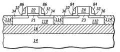
- FIG. 1includes an illustration of a cross-sectional view of a portion of a substrate 12 of a partially formed electronic device 10 , such as an integrated circuit.
- Substrate 12can include a monocrystalline semiconductor wafer, a semiconductor-on-insulator wafer, a flat panel display (e.g., a silicon layer over a glass plate), or other substrate conventionally used to form electronic devices.
- the upper surface of substrate 12is primary surface 13 .
- substrate 12includes a base material 14 , an insulating layer 16 and a semiconductor layer substantially having a (100) surface crystal orientation and channel lengths and channel widths along ⁇ 110> crystal directions.
- Field isolation regions 114can be formed leaving remaining portions of the semiconductor layer as active regions 110 and 112 .
- active region 110can be an n-channel active region and active region 112 can be a p-channel active region, and each of the active layers has a primary surface that is exposed that lies substantially along a (100) crystal plane.
- Gate dielectric layers 21 and 23 and gate electrodes 22 and 24are formed over the substrate 12 as illustrated in FIG. 2 .
- Gate dielectric layer 21can include a film of silicon dioxide, silicon nitride, silicon oxynitride, a high dielectric constant (“high-k”) material (e.g., dielectric constant greater than 8), or any combination thereof.
- high-khigh dielectric constant
- the high-k materialcan include Hf a O b N c , Hf a Si b O c , Hf a Si b O c N d , Hf a Zr b O c N d , Hf a Zr b Si c O d N e , Hf a Zr b O c , Zr a Si b O c , Zr a Si b O c N d , Zr a O b , other Hf-containing or Zr-containing dielectric material, a doped version of any of the foregoing (lanthanum doped, niobium doped, etc.), or any combination thereof.
- Gate dielectric layer 21can have a thickness in a range of approximately 1 to approximately 25 nm. Gate dielectric layer 21 may be thermally grown using an oxidizing or nitridizing ambient, or deposited using a conventional or proprietary chemical vapor deposition (“CVD”) technique, physical vapor deposition (“PVD”) technique, or a combination thereof. As compared to gate dielectric layer 21 , gate dielectric layer 23 can have the same or different materials, be formed at the same or different time, have the same or a different thickness, or any combination thereof.
- gate electrode 22can include a surface portion that substantially sets the work function for the transistor in the completed electronic device.
- the surface portioncan include a metallic element, such as a transition metal element.
- the surface portionmay include a second element that is silicon, oxygen, nitrogen or any combination thereof.
- the surface portion of gate electrode 22can include Ti a N b , Mo a N b , Mo a Si b N c , Ru a O b , Ir a O b , Ru, Ir, Mo a Si b O c , MO a Si b O c N d , Mo a Hf b O c , Mo a Hf b O c N d , other transition metal containing material, or any combination thereof.
- gate electrode 22may overlie the surface portion.
- the overlying portionis relatively more conductive as compared to the surface portion and can include a material such as amorphous silicon, polysilicon, a nitride, a metal-containing material, another suitable material, or any combination thereof.
- the materialcan include platinum, palladium, iridium, osmium, ruthenium, rhenium, indium-tin, indium-zinc, aluminum-tin, or any combination thereof.
- a material capable of reacting with silicon to form a silicideand can include Ti, Ta, Co, W, Mo, Zr, Pt, other suitable material, or any combination thereof is formed on gate electrode 22 and later reacted to form a metal silicide.
- gate electrode 22can include the relatively more conductive portion and may not include the surface portion. Gate electrode 22 can have a thickness of between approximately 30 and approximately 500 nm.
- Gate electrode 24can be formed using any combination of materials or techniques previously described for formation of gate electrode 22 .
- the materials, thicknesses techniques for forming portions of gate electrode 24 , time of formation, or any combination thereofcould be the same or different from those used to form portions of gate electrode 22 .
- the surface portion of gate electrode 24is different from the surface portion of gate electrode 22 .
- the surface portion for gate electrode 24can include Ta a C b , Ta a Si b N c , Ta a N b , Ta a Si b C c , Hf a C b , Nb a C b , Ti a C b , Ni a Si b , or any combination thereof.
- Gate electrode 24also includes a more conductive portion substantially similar to gate electrode 22 . The surface portion of gate electrode 24 is not required.
- Liner layer 32is formed over the substrate, as illustrated in FIG. 3 , using conventional or proprietary process.
- liner layer 32can include an oxide, a nitride, an oxynitride, or a combination thereof.
- liner layer 32has a thickness not greater than approximately 30 nm, in a particular embodiment, is not greater than approximately 20 nm in thickness, and in a more particular embodiment, is in a range of approximately 2 nm to approximately 15 nm.
- liner layer 32can be grown or deposited by a technique previously described for the gate dielectric layer 21 .
- Liner layer 32can protect the sidewalls of gate electrodes 22 and 24 by covering them during subsequent processing and can reduce the likelihood of implant channeling within the substrate when dopant species are implanted through liner layer 32 . Thus, liner layer 32 does not have a principal purpose of blocking implants. Liner layer 32 can serve as an etch stop layer during subsequent processing and can help reduce surface defects on exposed portions of partially formed electronic device 10 .
- a dopantcan be introduced to form doped regions 34 and 36 within active regions 110 and 112 , respectively.
- an n-type dopante.g. arsenic, phosphorus, antimony, or any combination thereof
- the dopantcan be introduced using ion implantation and activated during one or more subsequent thermal cycles.
- the doping concentration of doped regions 34is at least approximately 1E17 atoms/cm 3 .
- p-type dopant,(e.g. boron) is introduced into active region 112 adjacent to gate electrode 24 to form doped regions 36 .
- the dopantmay be introduced and activated as previously described for doped regions 34 .
- the doping concentration of doped regions 36is at least approximately 1E17 atoms/cm 3 .
- Layer 42is formed over liner layer 32 as illustrated in FIG. 4 using a conventional or proprietary process.
- layer 42can include silicon, polysilicon, an oxide, a nitride, an oxynitride, or a combination thereof.
- layer 42can be grown or deposited by a technique previously described for the gate dielectric portion of gate electrode 22 .
- layer 42has a thickness not greater than approximately 200 nm, in a particular embodiment, not greater than approximately 100 nm, and in a more particular embodiment, layer 42 is in a range of approximately 5 nm to 90 nm.
- layer 42is formed using a deposition process.
- deposition techniquescan include PVD, CVD, or any combination thereof.
- silicon nitride filmcan be formed with either tensile or compressive stress by varying a process parameter such as: pressure, temperature, gas ratio, power density, frequency, or any combination thereof.
- a process parametersuch as: pressure, temperature, gas ratio, power density, frequency, or any combination thereof.
- RFradio frequency
- the processcan be performed in a PRODUCERTM or CENTURATM chamber made by Applied Materials, Inc. of Santa Clara, Calif.
- the pressurecan be in a range of approximately 1 to approximately 10 torr, and in a particular embodiment, in a range of approximately 2 to approximately 6.5 torr.
- the chuck temperaturecan be in a range of approximately 200° C. to approximately 600° C., and in a particular embodiment, in a range of approximately 350° C. to approximately 600° C. Other considerations unrelated to stress may limit the temperature.
- the partially formed electronic device 10may only tolerate temperatures up to 450° C.
- the flow of nitrogen containing precursorcan be approximately between 1.5 and 5 times greater than the silicon-containing precursor.
- ammoniacan be the nitrogen-containing precursor
- silanecan be the silicon-containing precursor.
- the carrier gas streamcan include a relatively inert gas, such as nitrogen, helium, argon, or a combination thereof.
- the total RF power densitycan be in a range of approximately 0.050 to approximately 1.6 watts per square centimeter (“W/cm 2 ”) while the substrate spacing can be in a range of approximately 0.51 to approximately 1.52 cm.
- the total RF power densitycan be in a range of approximately 0.050 to approximately 0.80 W/cm 2 while the substrate spacing is in a range of approximately 0.050 and approximately 1.1 cm.
- the total RF power densitycan be in a range of approximately 0.050 to approximately 0.32 W/cm 2 while the spacing can be in a range of approximately 1.0 and approximately 1.3 cm.
- the RF powercan be at one or more frequencies, and therefore, total RF power density is the sum of the RF power at each frequency divided by the area of the primary surface 13 .
- layer 42can have compressive stress.
- the compressive stresscan have a magnitude not less than approximately 1.5 GPa (i.e., stress ⁇ 1.5 GPa), in a particular embodiment, not less than approximately 2.1 GPa (i.e., stress ⁇ 2.1 GPa), and in a more particular embodiment, not less than 2.5 GPa (i.e., stress ⁇ 2.3 GPa).
- layer 42can be chosen to have a more compressive stress than a subsequent layer used to form a sidewall spacer adjacent to a gate electrode.
- layer 42can be chosen to have a less tensile stress than a subsequent layer used to form a sidewall spacer adjacent to a gate electrode.
- a patterned masking layer 52is formed over active region 112 using a conventional or proprietary lithographic technique.
- the n-channel source drain implant maskis used to form the pattern.
- a custom maskis used.
- An exposed portion of layer 42is removed from active region 110 as illustrated in FIG. 5 .
- liner layer 32can act as an etch stop. The patterned masking layer 52 can then be removed.
- Layer 62can be formed over the workpiece as illustrated in FIG. 6 using a conventional or proprietary process. Layer 62 can be formed using materials or techniques described previously for forming layer 42 . Layer 62 can have the same thickness or different thickness as layer 42 .
- the stress of layer 62can be tensile.
- the tensile stresscan have a magnitude not less than approximately 0.6 GPa (i.e., stress ⁇ +0.6 GPa), in another embodiment, not less than approximately 1.0 GPa (i.e., stress ⁇ +1.0 GPa), and in a more particular embodiment, not less than approximately 1.5 GPa (i.e., stress ⁇ +1.5 GPa).
- a patterned masking layer 72is formed over active region 110 using a conventional or proprietary lithographic technique.
- the p-channel source drain implant maskcan be used to form the pattern.
- a custom maskis used.
- An exposed portion of layer 62is removed to expose a portion of layer 42 as illustrated in FIG. 7 .
- a wet etch processis used.
- Tensile stresscan increase the wet etch rate of films of similar compositions.
- a film with a higher value of stressi.e., more tensile
- layer 62can be tensile and layer 42 can be compressive
- layer 62can be more tensile and layer 42 can be less tensile
- layer 62can be less compressive and layer 42 can be more compressive.
- layer 62when layer 62 includes tensile silicon nitride and layer 42 includes compressive silicon nitride.
- An HF solutioncan be used as a wet chemical etchant and have a concentration in a range of approximately 10:1 (10 parts water to 1 part HF) to approximately 1000:1, and in a particular embodiment can be in a range of approximately 50:1 to approximately 200:1.
- layer 62etches at a rate at least approximately six times higher than layer 42 , and in a particular embodiment, etches at a rate in a range of approximately 10 to 15 times higher.
- wet chemical etchingcan be used to selectively remove portions of the layer 62 that overlie the remaining portions of layer 42 without removing too much of layer 42 .
- the patterned masking layer 72is then removed.
- each of sidewall spacers 84 and 86can have a shape that is substantially a half parabola, substantially rectangular, substantially triangular, substantially L-shaped, or the mirror image of said shape.
- Sidewall spacer 84substantially resides within a remaining portion of liner layer 32 such that at least a portion of liner layer 32 lies between sidewall spacer 84 and gate electrode 24 and another at least a portion of liner layer 32 lies between sidewall spacer 84 active region 112 .
- Sidewall spacer 86substantially resides within a remaining portion of liner layer 32 such that at least a portion of liner layer 32 lies between sidewall spacer 86 and gate electrode 22 and another at least a portion of liner layer 32 lies between sidewall spacer 86 active region 110 .
- remaining portions of liner layer 32are substantially L-shaped or the mirror image of L-shaped.
- Another dopantcan be introduced into doped regions 34 and 36 within active regions 110 and 112 , respectively, to complete formation of source/drain regions for the transistors structures.
- Sidewall spacer structures 84 and 86can serve to substantially shield underlying portions of substrate 12 from direct doping via ion implantation.
- an n-type dopante.g. arsenic, phosphorus, antimony, or any combination thereof
- the dopantcan be introduced using ion implantation and activated during one or more subsequent thermal cycles.
- the doping concentrationis at least approximately 1E19 atoms/cm 3 .
- a p-type dopant(e.g. boron) is introduced into active region 112 adjacent to sidewall spacer 84 .
- the dopantmay be introduced and activated as previously described for doped regions 34 .
- the doping concentration of doped regions 36is at least approximately 1E19 atoms/cm 3 .
- the exposed portions of liner layer 32can be removed, as illustrated in FIG. 8 , using a conventional or proprietary technique.
- transistor structures of electronic device 10are substantially complete.
- etch stop layer 92can now be formed as illustrated in FIG. 9 by conventional or proprietary processing.
- Etch stop layer 92has a composition chosen to be dissimilar than a subsequently formed premetal dielectric (PMD) layer.
- PMDpremetal dielectric
- etch stop layer 92can be formed using materials or techniques previously described for liner layer 32 .
- Etch stop layer 92may have a thickness no greater than approximately 100 nm.
- the etch stop layer 92comprises silicon nitride and has a relatively low magnitude of stress, as compared to layer 42 , 62 , or both.
- One or more insulating layers 104 , one or more conductive layers 106 , and one or more encapsulating layers 108are formed using one or more conventional or proprietary techniques as illustrated in FIG. 10 .
- processingproceeds as previously described through the structure described in FIG. 4 .
- Portions of layer 42are removed using a conventional or proprietary technique to form sidewall spacers 111 and 113 adjacent to gate electrodes 22 and 24 respectively, as illustrated in FIG. 11 .
- the electronic device 10can then be masked and sidewall spacer 111 can be removed using a conventional or proprietary technique.
- the n-channel source drain maskcan be used to provide the masking pattern.
- a custom maskcan provide the pattern.
- the mask(not illustrated) can then be removed, leaving the partially completed electronic device 10 as illustrated in FIG. 12 .
- Layer 62is formed overlying electronic device 10 as illustrated in FIG. 13 . A portion of layer 62 is removed using a conventional or proprietary technique to form sidewall spacer 142 adjacent to gate electrode 22 , as illustrated in FIG. 14 . An additional sidewall spacer (not illustrated) may or may not be formed adjacent to sidewall spacer 113 and gate electrode 24 at this time.
- a maskcan be formed over the active region 110 before performing the spacer etch. After forming the mask, at least a portion of layer 62 is removed using an HF solution, as previously described. The mask is removed, and sidewall spacer 142 is formed from the remaining portion of layer 62 using any one or more of the embodiments as previously described for sidewall spacer formation.
- each of sidewall spacers 113 and 142can have a shape and be located as previously described with respect to sidewall spacers 84 and 86 .
- sidewall spacers 113 and 142can have different shapes or widths from each other. Processing can continue as previously described for FIGS. 9 and 10 to form a substantially complete electronic device.
- a benefit of an exemplary, non-limiting embodimentincludes improved carrier mobility within a p-channel transistor structure having its channel lengths and channel widths along ⁇ 110> crystal directions.
- the improved carrier mobilitycan be achieved without using different widths of sidewall spacers. Less processing operations and higher component density and yield may be achieved. Still in one embodiment, different widths of sidewall spacers can be used and still not depart from the scope of the invention.
- an electronic devicecan include a p-channel transistor structure including a first gate electrode surrounded by a first sidewall spacer having a first stress, wherein the first sidewall spacer is an only sidewall spacer surrounding the first gate electrode or a closer sidewall spacer as compared to any other sidewall spacer that surrounds the first gate electrode.
- the electronic devicecan also include an n-channel transistor structure including a second gate electrode surrounded by a second sidewall spacer having second stress, wherein the second sidewall spacer is an only sidewall spacer surrounding the second gate electrode or a closer sidewall spacer as compared to any other sidewall spacer that surrounds the second gate electrode, wherein the first stress has a lower value of stress as compared to the second stress.
- the electronic devicecan further include a liner layer, wherein a first substantially L-shaped portion of the liner layer lies between the first sidewall spacer and the first gate electrode and between the first sidewall spacer and a first active region of the p-channel transistor structure.
- the liner layercan also include a second substantially L-shaped portion of the liner layer lies between the second sidewall spacer and the second gate electrode and between the second sidewall spacer and a second active region of the n-channel transistor structure.
- each of the first and second sidewall spacershas a shape that is substantially a half parabola, substantially rectangular, or substantially triangular.
- each of the first and second sidewall spacershas a shape that is substantially L-shaped.
- the p-channel transistor structurefurther includes a first active region having a first primary surface
- the n-channel transistor structurefurther includes a second active region having a second primary surface. Each of the first and second primary surfaces lies substantially along a (100) crystal plane.
- the first sidewall spaceris the only sidewall spacer surrounding the first gate electrode, and the second sidewall spacer is the only sidewall spacer surrounding the second gate electrode.
- a process for forming an electronic devicecan include providing a substrate.
- the processcan also include forming a first gate electrode of a first transistor structure over the substrate, wherein the first transistor structure includes a first channel region, and forming a second gate electrode of a second transistor structure over the substrate, wherein the second transistor structure includes a second channel region that has a conductivity type opposite that of the first channel region.
- the processcan further include forming a first layer over the first and second gate electrodes and the substrate, wherein the first layer has a first stress, and removing a first portion of the first layer that overlies the second transistor structure.
- the processcan also include forming a second layer over the first and second gate electrodes and the substrate, wherein the second layer has a second stress different from the first stress, and removing a second portion of the second layer that overlies the first transistor structure.
- the processcan still further include forming a first sidewall spacer that surrounds the first gate electrode after removing the first portion of the first layer and removing the second portion of the second layer, wherein the first sidewall spacer is formed before forming any other sidewall spacer that surrounds the first gate electrode.
- the processcan also include forming a second sidewall spacer that surrounds the second gate electrode after removing the first portion of the first layer and removing the second portion of the second layer, wherein the second sidewall spacer is formed before forming any other sidewall spacer that surrounds the second gate electrode.
- the first transistor structureis a p-channel transistor structure
- the second transistor substrateis an n-channel transistor structure.
- the first stresshas a lower value as compared to the second stress.
- forming the first layeris performed before forming the second layer.
- forming the first layeris performed after forming the second layer.
- forming the first sidewall spacer and forming the second sidewall spacerare performed during a same etch operation.
- the processcan further include forming a liner layer after forming the first gate electrode, after forming the second gate electrode, before forming the first layer, and before forming the second layer.
- forming the first gate electrodefurther includes forming the first gate electrode, wherein the first active region has a first primary surface
- forming the second gate electrodefurther includes forming the second gate electrode, wherein the second active region has a second primary surface.
- Each of the first and second primary surfaceslies substantially along a (100) crystal plane.
- a process for forming an electronic devicecan include providing a substrate.
- the processcan also include forming a first gate electrode of a first transistor structure over the substrate, wherein the first transistor structure includes a first channel region, and forming a second gate electrode of a second transistor structure over the substrate, wherein the second transistor structure includes a second channel region that has a conductivity type opposite that of the first channel region.
- the processcan also include forming a first sidewall spacer that surrounds the first gate electrode and a second sidewall spacer that surrounds the second gate electrode, wherein the first and second sidewall spacers have a first stress and removing the second sidewall spacer.
- the processcan also include forming a third sidewall spacer that surrounds the second gate electrode, wherein the third sidewall spacer is formed after removing the second sidewall spacer and has a second stress different from the first stress.
- the first sidewall spaceris an only sidewall spacer surrounding the first gate electrode or a closer sidewall spacer as compared to any other sidewall spacer that surrounds the first gate electrode.
- the third sidewall spaceris an only sidewall spacer surrounding the second gate electrode or a closer sidewall spacer as compared to any other sidewall spacer that surrounds the second gate electrode.
- the first transistor structureis a p-channel transistor structure
- the second transistor substrateis an n-channel transistor structure
- the first stresshas a lower value as compared to the second stress.
- forming the third sidewall spacerincludes forming a tensile silicon nitride layer over the first gate electrode, the second gate electrode, the first sidewall spacer, and the substrate, and forming a mask including an opening. An exposed portion of the tensile silicon nitride layer that overlies the first gate electrode and the first sidewall spacer is exposed along a bottom of the opening, and the mask covers the second gate electrode.
- the processcan also include removing the exposed portion of the tensile silicon nitride layer using an HF solution.
- forming the first and second sidewall spacersincludes forming the first and second sidewall spacers that include a compressive silicon nitride layer.
- removing the exposed portion of the tensile silicon nitride layerincludes removing the exposed portion of the tensile silicon nitride layer, such that the HF solution has a selectivity, wherein tensile silicon nitride can be etched at least approximately 6 times faster than compressive silicon nitride.
- the processcan further include forming a liner layer after forming the first gate electrode, after forming the second gate electrode, and before forming the first and second sidewall spacers.
- forming the first gate electrodefurther includes forming the first gate electrode, wherein the first active region has a first primary surface
- forming the second gate electrodefurther includes forming the second gate electrode, wherein the second active region has a second primary surface.
- Each of the first and second primary surfaceslies substantially along a (100) crystal plane.
Landscapes
- Metal-Oxide And Bipolar Metal-Oxide Semiconductor Integrated Circuits (AREA)
- Insulated Gate Type Field-Effect Transistor (AREA)
Abstract
Description
- 1. Field of the Disclosure
- The present invention relates to electronic devices and processes for forming electronic devices, and more particularly, to electronic devices including transistor structures with sidewall spacers and processes for forming the electronic devices.
- 2. Description of the Related Art
- Semiconductor-on-insulator (“SOI”) architectures are becoming the more common as electronic and device performance requirements continue to be more demanding. P-channel and n-channel transistors formed using an SOI substrate typically include active regions that have channel lengths and channel widths along <110> crystal directions. Carrier mobility within the channel regions of the p-channel and n-channel transistors is an area for continued improvement.
- Many approaches use different widths of sidewall spacers to affect the performance of the transistors. For example, relatively narrower sidewall spacers can be formed adjacent to gate electrodes of n-channel transistors, and relatively wider sidewall spacers can be formed adjacent to gate electrodes of p-channel transistors. The different widths of sidewall spacers can involve additional or more complex processing operations and result in transistors, particularly p-channel transistors that may need to be designed wider to account for the wider sidewall spacers. Lower component density and decreased yield may occur with the sidewall spacers of differing widths.
- The invention is illustrated by way of example and not limitation in the accompanying figures.
FIG. 1 includes an illustration of a cross-sectional view of a portion of a workpiece including an n-channel active and a p-channel active region.FIG. 2 includes an illustration of a cross-sectional view of the workpiece ofFIG. 1 after formation of gate electrodes.FIG. 3 includes an illustration of a cross-sectional view of a workpiece ofFIG. 2 after formation of doped regions.FIG. 4 includes an illustration of a cross-sectional view of the workpiece ofFIG. 3 after formation of a sidewall spacer layer.FIG. 5 includes an illustration of a cross-sectional view of the workpiece ofFIG. 4 after removal of the sidewall spacer layer from over the n-channel active region.FIG. 6 includes an illustration of a cross-sectional view of the workpiece ofFIG. 5 after formation of another sidewall spacer layer.FIG. 7 includes an illustration of a cross-sectional view of the workpiece inFIG. 6 after removal of another sidewall spacer layer from over the p-channel active region.FIG. 8 includes an illustration of a cross-sectional view of the workpiece ofFIG. 7 after formation of sidewall spacers.FIG. 9 includes an illustration of a cross-sectional view of the workpiece ofFIG. 8 after formation of an etch-stop layer.FIG. 10 includes an illustration of a cross-sectional view of the workpiece ofFIG. 9 after substantial completion of the electronic device.FIG. 11 includes an illustration of a cross-sectional view of the workpiece ofFIG. 4 after formation of sidewall spacers.FIG. 12 includes an illustration of a cross-sectional view of the workpiece of FIG. I1 after removal of a sidewall spacer from over the n-channel active region.FIG. 13 includes an illustration of a cross-sectional view of the workpiece ofFIG. 12 after formation of another sidewall spacer layer.FIG. 14 includes an illustration of a cross-sectional view of the workpiece ofFIG. 13 after formation of another sidewall spacer.- Skilled artisans appreciate that elements in the figures are illustrated for simplicity and clarity and have not necessarily been drawn to scale. For example, the dimensions of some of the elements in the figures may be exaggerated relative to other elements to help to improve understanding of embodiments of the invention.
- An electronic device can include a first transistor structure including a first gate electrode surrounded by a first sidewall spacer having a first stress and a second transistor structure including a second gate electrode surrounding a second sidewall spacer having second stress. The first sidewall spacer is an only sidewall spacer surrounding the first gate electrode or a closer sidewall spacer as compared to any other sidewall spacer that surrounds the first gate electrode and the second sidewall spacer is an only sidewall spacer surrounding the second gate electrode or a closer sidewall spacer as compared to any other sidewall spacer that surrounds the second gate electrode, wherein the first stress has a lower value as compared to the second stress. In a particular embodiment, the first transistor structure can be a p-channel transistor structure, and the second transistor structure can be an n-channel transistor structure. More than one process can be used to form the electronic device.
- Before addressing details of embodiments described below, some terms are defined or clarified. The term “active region” is intended to mean part of a transistor structure through which carriers are designed to flow. The active region includes a channel region, a source region, a drain region, a source/drain region, or any combination thereof for one or more transistor structures.
- The term “primary surface” is intended to mean a surface from which a transistor structure is subsequently formed. The primary surface may be an original surface of a base material before forming any electronic components or may be a surface of a semiconductor layer that overlies the base material. For example, an exposed surface of a semiconductor layer of a semiconductor-on-insulator substrate can be a primary surface, and not the original surface of the base material.
- The term “sidewall spacer” is intended to mean a structure that has a principal purpose of substantially blocking an implant near an edge of a feature, such that, from a top view, an implanted region, formed after the spacer has been formed, is offset from the edge. The feature may be within or over a substrate, and the edge may be substantially vertical or sloped.
- The term “stress” is intended to mean the composite force resulting from two dissimilar materials contacting each other. Stress can be compressive, zero, or tensile. As used in this specification, compressive stress has a negative value, and tensile stress has a positive value. When comparing values of stresses, actual values, and not absolute values, are used. For example, a first layer having a stress of −2.1 GPa has a lower value as compared to a second layer having a stress of −1.6 GPa, even though the first layer is more compressive as compared to the second layer. Unless stated expressly to the contrary, stress of a layer is measured after depositing the layer and before the layer is exposed to any subsequent thermal cycle.
- The term “transistor structure” is intended to mean a gate electrode and associated channel region, source and drain regions or source/drain regions. A gate dielectric layer may or may not be part of the transistor structure. A transistor structure can be configured to function as a transistor, a capacitor, or a resistor.
- As used herein, the terms “comprises,” “comprising,” “includes,” “including,” “has,” “having” or any other variation thereof, are intended to cover a non-exclusive inclusion. For example, a process, method, article, or apparatus that comprises a list of elements is not necessarily limited to only those elements but may include other elements not expressly listed or inherent to such process, method, article, or apparatus. Further, unless expressly stated to the contrary, “or” refers to an inclusive or and not to an exclusive or. For example, a condition A or B is satisfied by any one of the following: A is true (or present) and B is false (or not present), A is false (or not present) and B is true (or present), and both A and B are true (or present).
- Additionally, for clarity purposes and to give a general sense of the scope of the embodiments described herein, the use of the “a” or “an” are employed to describe one or more articles to which “a” or “an” refers. Therefore, the description should be read to include one or at least one whenever “a” or “an” is used, and the singular also includes the plural unless it is clear that the contrary is meant otherwise.
- Unless otherwise defined, all technical and scientific terms used herein have the same meaning as commonly understood by one of ordinary skill in the art to which this invention belongs. All publications, patent applications, patents, and other references mentioned herein are incorporated by reference in their entirety. In case of conflict, the present specification, including definitions, will control. In addition, the materials, methods, and examples are illustrative only and not intended to be limiting.
- Other features and advantages of the invention will be apparent from the following detailed description, and from the claims.
- To the extent not described herein, many details regarding specific materials, processing acts, and circuits are conventional and may be found in textbooks and other sources within the semiconductor and microelectronic arts.
FIG. 1 includes an illustration of a cross-sectional view of a portion of asubstrate 12 of a partially formedelectronic device 10, such as an integrated circuit.Substrate 12 can include a monocrystalline semiconductor wafer, a semiconductor-on-insulator wafer, a flat panel display (e.g., a silicon layer over a glass plate), or other substrate conventionally used to form electronic devices. The upper surface ofsubstrate 12 isprimary surface 13. In one embodiment,substrate 12 includes abase material 14, an insulatinglayer 16 and a semiconductor layer substantially having a (100) surface crystal orientation and channel lengths and channel widths along <110> crystal directions.Field isolation regions 114 can be formed leaving remaining portions of the semiconductor layer asactive regions active region 110 can be an n-channel active region andactive region 112 can be a p-channel active region, and each of the active layers has a primary surface that is exposed that lies substantially along a (100) crystal plane.- Gate dielectric layers21 and23 and
gate electrodes substrate 12 as illustrated inFIG. 2 .Gate dielectric layer 21 can include a film of silicon dioxide, silicon nitride, silicon oxynitride, a high dielectric constant (“high-k”) material (e.g., dielectric constant greater than 8), or any combination thereof. The high-k material can include HfaObNc, HfaSibOc, HfaSibOcNd, HfaZrbOcNd, HfaZrbSicOdNe, HfaZrbOc, ZraSibOc, ZraSibOcNd, ZraOb, other Hf-containing or Zr-containing dielectric material, a doped version of any of the foregoing (lanthanum doped, niobium doped, etc.), or any combination thereof. As used herein, subscripts on compound materials specified with alphabetic subscripts are intended to represent the non-zero fraction of the atomic species present in that compound, and therefore, the alphabetic subscripts within a compound sum to 1. For example, in the case of HfaObNc, the sum of “a,” “b,” and “c” is 1.Gate dielectric layer 21 can have a thickness in a range of approximately 1 to approximately 25 nm.Gate dielectric layer 21 may be thermally grown using an oxidizing or nitridizing ambient, or deposited using a conventional or proprietary chemical vapor deposition (“CVD”) technique, physical vapor deposition (“PVD”) technique, or a combination thereof. As compared togate dielectric layer 21,gate dielectric layer 23 can have the same or different materials, be formed at the same or different time, have the same or a different thickness, or any combination thereof. - In one embodiment,
gate electrode 22 can include a surface portion that substantially sets the work function for the transistor in the completed electronic device. In a more particular embodiment, the surface portion can include a metallic element, such as a transition metal element. In another embodiment, the surface portion may include a second element that is silicon, oxygen, nitrogen or any combination thereof. The surface portion ofgate electrode 22 can include TiaNb, MoaNb, MoaSibNc, RuaOb, IraOb, Ru, Ir, MoaSibOc, MOaSibOcNd, MoaHfbOc, MoaHfbOcNd, other transition metal containing material, or any combination thereof. - Another portion of
gate electrode 22 may overlie the surface portion. In one embodiment, the overlying portion is relatively more conductive as compared to the surface portion and can include a material such as amorphous silicon, polysilicon, a nitride, a metal-containing material, another suitable material, or any combination thereof. In one embodiment, the material can include platinum, palladium, iridium, osmium, ruthenium, rhenium, indium-tin, indium-zinc, aluminum-tin, or any combination thereof. In another embodiment, a material capable of reacting with silicon to form a silicide, and can include Ti, Ta, Co, W, Mo, Zr, Pt, other suitable material, or any combination thereof is formed ongate electrode 22 and later reacted to form a metal silicide. In another embodiment,gate electrode 22 can include the relatively more conductive portion and may not include the surface portion.Gate electrode 22 can have a thickness of between approximately 30 and approximately 500 nm. Gate electrode 24 can be formed using any combination of materials or techniques previously described for formation ofgate electrode 22. The materials, thicknesses techniques for forming portions ofgate electrode 24, time of formation, or any combination thereof could be the same or different from those used to form portions ofgate electrode 22. In one embodiment, the surface portion ofgate electrode 24 is different from the surface portion ofgate electrode 22. In a more particular embodiment, the surface portion forgate electrode 24 can include TaaCb, TaaSibNc, TaaNb, TaaSibCc, HfaCb, NbaCb, TiaCb, NiaSib, or any combination thereof.Gate electrode 24 also includes a more conductive portion substantially similar togate electrode 22. The surface portion ofgate electrode 24 is not required.Liner layer 32 is formed over the substrate, as illustrated inFIG. 3 , using conventional or proprietary process. In one embodiment,liner layer 32 can include an oxide, a nitride, an oxynitride, or a combination thereof. In another embodiment,liner layer 32 has a thickness not greater than approximately 30 nm, in a particular embodiment, is not greater than approximately 20 nm in thickness, and in a more particular embodiment, is in a range of approximately 2 nm to approximately 15 nm. In still another embodiment,liner layer 32 can be grown or deposited by a technique previously described for thegate dielectric layer 21.Liner layer 32 can protect the sidewalls ofgate electrodes liner layer 32. Thus,liner layer 32 does not have a principal purpose of blocking implants.Liner layer 32 can serve as an etch stop layer during subsequent processing and can help reduce surface defects on exposed portions of partially formedelectronic device 10.- A dopant can be introduced to form doped
regions active regions active region 110 adjacent togate electrode 22 to form dopedregions 34. In a specific embodiment, the dopant can be introduced using ion implantation and activated during one or more subsequent thermal cycles. In another embodiment, the doping concentration ofdoped regions 34 is at least approximately 1E17 atoms/cm3. In a further embodiment, p-type dopant, (e.g. boron) is introduced intoactive region 112 adjacent togate electrode 24 to form dopedregions 36. The dopant may be introduced and activated as previously described fordoped regions 34. In one embodiment, the doping concentration ofdoped regions 36 is at least approximately 1E17 atoms/cm3. Layer 42 is formed overliner layer 32 as illustrated inFIG. 4 using a conventional or proprietary process. In one embodiment,layer 42 can include silicon, polysilicon, an oxide, a nitride, an oxynitride, or a combination thereof. In another embodiment,layer 42 can be grown or deposited by a technique previously described for the gate dielectric portion ofgate electrode 22. In still another embodiment,layer 42 has a thickness not greater than approximately 200 nm, in a particular embodiment, not greater than approximately 100 nm, and in a more particular embodiment,layer 42 is in a range of approximately 5 nm to 90 nm.- In one embodiment,
layer 42 is formed using a deposition process. Such deposition techniques can include PVD, CVD, or any combination thereof. In one particular embodiment, using a plasma-enhanced CVD process, silicon nitride film can be formed with either tensile or compressive stress by varying a process parameter such as: pressure, temperature, gas ratio, power density, frequency, or any combination thereof. One skilled in the art can appreciate that at least some of these factors can interact with each other, the physical arrangement of the reactor vessel, and one or more exposed surfaces of the workpiece. In one embodiment, the reactor vessel is a portion of a substrate-processing tool with a dual frequency radio frequency (“RF”) generator and a height-adjustable chuck designed for processing substrates with a nominal diameter of 200 mm. In a specific embodiment, the process can be performed in a PRODUCER™ or CENTURA™ chamber made by Applied Materials, Inc. of Santa Clara, Calif. In one embodiment, the pressure can be in a range of approximately 1 to approximately 10 torr, and in a particular embodiment, in a range of approximately 2 to approximately 6.5 torr. In another embodiment, the chuck temperature can be in a range of approximately 200° C. to approximately 600° C., and in a particular embodiment, in a range of approximately 350° C. to approximately 600° C. Other considerations unrelated to stress may limit the temperature. For example, the partially formedelectronic device 10 may only tolerate temperatures up to 450° C. - In another embodiment, when a nitrogen-containing precursor and a silicon-containing precursor are used to form a silicon nitride film, the flow of nitrogen containing precursor can be approximately between 1.5 and 5 times greater than the silicon-containing precursor. In a more particular embodiment, ammonia can be the nitrogen-containing precursor, and silane can be the silicon-containing precursor. In an even more particular embodiment, the carrier gas stream can include a relatively inert gas, such as nitrogen, helium, argon, or a combination thereof. In one embodiment, the total RF power density can be in a range of approximately 0.050 to approximately 1.6 watts per square centimeter (“W/cm2”) while the substrate spacing can be in a range of approximately 0.51 to approximately 1.52 cm. In a more specific embodiment, for compressive silicon nitride film, the total RF power density can be in a range of approximately 0.050 to approximately 0.80 W/cm2while the substrate spacing is in a range of approximately 0.050 and approximately 1.1 cm. In another more specific embodiment, for a tensile silicon nitride film, the total RF power density can be in a range of approximately 0.050 to approximately 0.32 W/cm2while the spacing can be in a range of approximately 1.0 and approximately 1.3 cm. The RF power can be at one or more frequencies, and therefore, total RF power density is the sum of the RF power at each frequency divided by the area of the
primary surface 13. - In one embodiment,
layer 42 can have compressive stress. In a particular embodiment, the compressive stress can have a magnitude not less than approximately 1.5 GPa (i.e., stress ≦−1.5 GPa), in a particular embodiment, not less than approximately 2.1 GPa (i.e., stress ≦−2.1 GPa), and in a more particular embodiment, not less than 2.5 GPa (i.e., stress ≦−2.3 GPa). In another embodiment,layer 42 can be chosen to have a more compressive stress than a subsequent layer used to form a sidewall spacer adjacent to a gate electrode. In still another embodiment,layer 42 can be chosen to have a less tensile stress than a subsequent layer used to form a sidewall spacer adjacent to a gate electrode. - A
patterned masking layer 52 is formed overactive region 112 using a conventional or proprietary lithographic technique. In one particular embodiment, the n-channel source drain implant mask is used to form the pattern. In another embodiment, a custom mask is used. An exposed portion oflayer 42 is removed fromactive region 110 as illustrated in FIG.5. In a particular embodiment,liner layer 32 can act as an etch stop. The patternedmasking layer 52 can then be removed. Layer 62 can be formed over the workpiece as illustrated inFIG. 6 using a conventional or proprietary process.Layer 62 can be formed using materials or techniques described previously for forminglayer 42.Layer 62 can have the same thickness or different thickness aslayer 42. In one embodiment, the stress oflayer 62 can be tensile. In a particular embodiment, the tensile stress can have a magnitude not less than approximately 0.6 GPa (i.e., stress ≧+0.6 GPa), in another embodiment, not less than approximately 1.0 GPa (i.e., stress ≧+1.0 GPa), and in a more particular embodiment, not less than approximately 1.5 GPa (i.e., stress ≧+1.5 GPa).- A
patterned masking layer 72 is formed overactive region 110 using a conventional or proprietary lithographic technique. In one particular embodiment, the p-channel source drain implant mask can be used to form the pattern. In another embodiment, a custom mask is used. An exposed portion oflayer 62 is removed to expose a portion oflayer 42 as illustrated inFIG. 7 . In one embodiment, a wet etch process is used. Tensile stress can increase the wet etch rate of films of similar compositions. A film with a higher value of stress (i.e., more tensile) can have a higher chemical etch rate than a film of substantially the same composition with a lower value of stress (i.e., more compressive). For example,layer 62 can be tensile andlayer 42 can be compressive,layer 62 can be more tensile andlayer 42 can be less tensile, orlayer 62 can be less compressive andlayer 42 can be more compressive. - In one non-limiting embodiment, when
layer 62 includes tensile silicon nitride andlayer 42 includes compressive silicon nitride. An HF solution can be used as a wet chemical etchant and have a concentration in a range of approximately 10:1 (10 parts water to 1 part HF) to approximately 1000:1, and in a particular embodiment can be in a range of approximately 50:1 to approximately 200:1. In a particular embodiment,layer 62 etches at a rate at least approximately six times higher thanlayer 42, and in a particular embodiment, etches at a rate in a range of approximately 10 to 15 times higher. Thus, wet chemical etching can be used to selectively remove portions of thelayer 62 that overlie the remaining portions oflayer 42 without removing too much oflayer 42. The patternedmasking layer 72 is then removed. - The remaining portion of
layer 42 overliesactive region 112, and the remaining portion oflayer 62 overliesactive region 110. In a particular embodiment, remaining portions oflayer 42 can be compressive and remaining portions oflayer 62 can be tensile. Portions of the composite layer are removed using a conventional or proprietary process to formsidewall spacers gate electrode structures sidewall spacers Sidewall spacer 84 substantially resides within a remaining portion ofliner layer 32 such that at least a portion ofliner layer 32 lies betweensidewall spacer 84 andgate electrode 24 and another at least a portion ofliner layer 32 lies betweensidewall spacer 84active region 112.Sidewall spacer 86 substantially resides within a remaining portion ofliner layer 32 such that at least a portion ofliner layer 32 lies betweensidewall spacer 86 andgate electrode 22 and another at least a portion ofliner layer 32 lies betweensidewall spacer 86active region 110. In one embodiment, in a cross-sectional view, remaining portions ofliner layer 32 are substantially L-shaped or the mirror image of L-shaped. - Another dopant (not illustrated) can be introduced into doped
regions active regions Sidewall spacer structures substrate 12 from direct doping via ion implantation. In one embodiment, an n-type dopant, (e.g. arsenic, phosphorus, antimony, or any combination thereof) is introduced intoactive region 110 adjacent tosidewall spacer 86. In a specific embodiment, the dopant can be introduced using ion implantation and activated during one or more subsequent thermal cycles. In another embodiment, the doping concentration is at least approximately 1E19 atoms/cm3. A p-type dopant (e.g. boron) is introduced intoactive region 112 adjacent tosidewall spacer 84. The dopant may be introduced and activated as previously described fordoped regions 34. In one embodiment, the doping concentration ofdoped regions 36 is at least approximately 1E19 atoms/cm3. Optionally, the exposed portions ofliner layer 32 can be removed, as illustrated inFIG. 8 , using a conventional or proprietary technique. In one embodiment, transistor structures ofelectronic device 10 are substantially complete. - Processing can be continued to form a substantially completed electronic device. An
etch stop layer 92 can now be formed as illustrated inFIG. 9 by conventional or proprietary processing.Etch stop layer 92 has a composition chosen to be dissimilar than a subsequently formed premetal dielectric (PMD) layer. In one embodiment,etch stop layer 92 can be formed using materials or techniques previously described forliner layer 32.Etch stop layer 92 may have a thickness no greater than approximately 100 nm. In a particular embodiment, theetch stop layer 92 comprises silicon nitride and has a relatively low magnitude of stress, as compared tolayer insulating layers 104, one or moreconductive layers 106, and one or more encapsulating layers108 are formed using one or more conventional or proprietary techniques as illustrated inFIG. 10 . - In an alternative embodiment, processing proceeds as previously described through the structure described in
FIG. 4 . Portions oflayer 42 are removed using a conventional or proprietary technique to formsidewall spacers gate electrodes FIG. 11 . Theelectronic device 10 can then be masked andsidewall spacer 111 can be removed using a conventional or proprietary technique. In one embodiment, the n-channel source drain mask can be used to provide the masking pattern. In another embodiment, a custom mask can provide the pattern. The mask (not illustrated) can then be removed, leaving the partially completedelectronic device 10 as illustrated inFIG. 12 . Layer 62 is formed overlyingelectronic device 10 as illustrated inFIG. 13 . A portion oflayer 62 is removed using a conventional or proprietary technique to formsidewall spacer 142 adjacent togate electrode 22, as illustrated inFIG. 14 . An additional sidewall spacer (not illustrated) may or may not be formed adjacent tosidewall spacer 113 andgate electrode 24 at this time.- In one particular embodiment (not illustrated), a mask can be formed over the
active region 110 before performing the spacer etch. After forming the mask, at least a portion oflayer 62 is removed using an HF solution, as previously described. The mask is removed, andsidewall spacer 142 is formed from the remaining portion oflayer 62 using any one or more of the embodiments as previously described for sidewall spacer formation. - In one embodiment, in a cross-sectional view, each of
sidewall spacers sidewall spacers sidewall spacers FIGS. 9 and 10 to form a substantially complete electronic device. - A benefit of an exemplary, non-limiting embodiment includes improved carrier mobility within a p-channel transistor structure having its channel lengths and channel widths along <110> crystal directions. The improved carrier mobility can be achieved without using different widths of sidewall spacers. Less processing operations and higher component density and yield may be achieved. Still in one embodiment, different widths of sidewall spacers can be used and still not depart from the scope of the invention.
- Many different aspects and embodiments are possible. Some of those aspects and embodiments are described below. After reading this specification, skilled artisans will appreciate that those aspects and embodiments are only illustrative and do not limit the scope of the present invention.
- In a first aspect, an electronic device can include a p-channel transistor structure including a first gate electrode surrounded by a first sidewall spacer having a first stress, wherein the first sidewall spacer is an only sidewall spacer surrounding the first gate electrode or a closer sidewall spacer as compared to any other sidewall spacer that surrounds the first gate electrode. The electronic device can also include an n-channel transistor structure including a second gate electrode surrounded by a second sidewall spacer having second stress, wherein the second sidewall spacer is an only sidewall spacer surrounding the second gate electrode or a closer sidewall spacer as compared to any other sidewall spacer that surrounds the second gate electrode, wherein the first stress has a lower value of stress as compared to the second stress.
- In one embodiment of the first aspect, the electronic device can further include a liner layer, wherein a first substantially L-shaped portion of the liner layer lies between the first sidewall spacer and the first gate electrode and between the first sidewall spacer and a first active region of the p-channel transistor structure. The liner layer can also include a second substantially L-shaped portion of the liner layer lies between the second sidewall spacer and the second gate electrode and between the second sidewall spacer and a second active region of the n-channel transistor structure.
- In another embodiment of the first aspect, from a cross-sectional view, each of the first and second sidewall spacers has a shape that is substantially a half parabola, substantially rectangular, or substantially triangular. In still another embodiment, from a cross-sectional view, each of the first and second sidewall spacers has a shape that is substantially L-shaped. In yet another embodiment of the first aspect, the p-channel transistor structure further includes a first active region having a first primary surface, and the n-channel transistor structure further includes a second active region having a second primary surface. Each of the first and second primary surfaces lies substantially along a (100) crystal plane.
- In another embodiment of the first aspect, the first sidewall spacer is the only sidewall spacer surrounding the first gate electrode, and the second sidewall spacer is the only sidewall spacer surrounding the second gate electrode.
- In a second aspect, a process for forming an electronic device can include providing a substrate. The process can also include forming a first gate electrode of a first transistor structure over the substrate, wherein the first transistor structure includes a first channel region, and forming a second gate electrode of a second transistor structure over the substrate, wherein the second transistor structure includes a second channel region that has a conductivity type opposite that of the first channel region. The process can further include forming a first layer over the first and second gate electrodes and the substrate, wherein the first layer has a first stress, and removing a first portion of the first layer that overlies the second transistor structure. The process can also include forming a second layer over the first and second gate electrodes and the substrate, wherein the second layer has a second stress different from the first stress, and removing a second portion of the second layer that overlies the first transistor structure. The process can still further include forming a first sidewall spacer that surrounds the first gate electrode after removing the first portion of the first layer and removing the second portion of the second layer, wherein the first sidewall spacer is formed before forming any other sidewall spacer that surrounds the first gate electrode. The process can also include forming a second sidewall spacer that surrounds the second gate electrode after removing the first portion of the first layer and removing the second portion of the second layer, wherein the second sidewall spacer is formed before forming any other sidewall spacer that surrounds the second gate electrode.
- In one embodiment of the second aspect, the first transistor structure is a p-channel transistor structure, and the second transistor substrate is an n-channel transistor structure. The first stress has a lower value as compared to the second stress. In a particular embodiment, forming the first layer is performed before forming the second layer. In another particular embodiment, forming the first layer is performed after forming the second layer. In another embodiment, forming the first sidewall spacer and forming the second sidewall spacer are performed during a same etch operation.
- In still another embodiment of the second aspect, the process can further include forming a liner layer after forming the first gate electrode, after forming the second gate electrode, before forming the first layer, and before forming the second layer. In yet another embodiment, forming the first gate electrode further includes forming the first gate electrode, wherein the first active region has a first primary surface, and forming the second gate electrode further includes forming the second gate electrode, wherein the second active region has a second primary surface. Each of the first and second primary surfaces lies substantially along a (100) crystal plane.
- In a third aspect, a process for forming an electronic device can include providing a substrate. The process can also include forming a first gate electrode of a first transistor structure over the substrate, wherein the first transistor structure includes a first channel region, and forming a second gate electrode of a second transistor structure over the substrate, wherein the second transistor structure includes a second channel region that has a conductivity type opposite that of the first channel region. The process can also include forming a first sidewall spacer that surrounds the first gate electrode and a second sidewall spacer that surrounds the second gate electrode, wherein the first and second sidewall spacers have a first stress and removing the second sidewall spacer. The process can also include forming a third sidewall spacer that surrounds the second gate electrode, wherein the third sidewall spacer is formed after removing the second sidewall spacer and has a second stress different from the first stress. After forming the third sidewall spacer, the first sidewall spacer is an only sidewall spacer surrounding the first gate electrode or a closer sidewall spacer as compared to any other sidewall spacer that surrounds the first gate electrode. The third sidewall spacer is an only sidewall spacer surrounding the second gate electrode or a closer sidewall spacer as compared to any other sidewall spacer that surrounds the second gate electrode.
- In one embodiment of the third aspect, the first transistor structure is a p-channel transistor structure, the second transistor substrate is an n-channel transistor structure, and the first stress has a lower value as compared to the second stress. In another embodiment, forming the third sidewall spacer includes forming a tensile silicon nitride layer over the first gate electrode, the second gate electrode, the first sidewall spacer, and the substrate, and forming a mask including an opening. An exposed portion of the tensile silicon nitride layer that overlies the first gate electrode and the first sidewall spacer is exposed along a bottom of the opening, and the mask covers the second gate electrode. The process can also include removing the exposed portion of the tensile silicon nitride layer using an HF solution.
- In a particular embodiment of the third aspect, forming the first and second sidewall spacers includes forming the first and second sidewall spacers that include a compressive silicon nitride layer. In a more particular embodiment, removing the exposed portion of the tensile silicon nitride layer includes removing the exposed portion of the tensile silicon nitride layer, such that the HF solution has a selectivity, wherein tensile silicon nitride can be etched at least approximately 6 times faster than compressive silicon nitride.
- In another embodiment, the process can further include forming a liner layer after forming the first gate electrode, after forming the second gate electrode, and before forming the first and second sidewall spacers. In still another embodiment of the third aspect, forming the first gate electrode further includes forming the first gate electrode, wherein the first active region has a first primary surface, and forming the second gate electrode further includes forming the second gate electrode, wherein the second active region has a second primary surface. Each of the first and second primary surfaces lies substantially along a (100) crystal plane.
- Note that not all of the activities described above in the general description or the examples are required, that a portion of a specific activity may not be required, and that one or more further activities may be performed in addition to those described. Still further, the order in which activities are listed are not necessarily the order in which they are performed. After reading this specification, skilled artisans will be capable of determining which one or more activities or one or more portions thereof are used or not used and the order of such activities are to be performed for their specific needs or desires.
- Any one or more benefits, one or more other advantages, one or more solutions to one or more problems, or any combination thereof have been described above with regard to one or more specific embodiments. However, the benefit(s), advantage(s), solution(s) to problem(s), or any element(s) that may cause any benefit, advantage, or solution to occur or become more pronounced is not to be construed as a critical, required, or essential feature or element of any or all the claims.
- The above-disclosed subject matter is to be considered illustrative, and not restrictive, and the appended claims are intended to cover all such modifications, enhancements, and other embodiments that fall within the scope of the present invention. Thus, to the maximum extent allowed by law, the scope of the present invention is to be determined by the broadest permissible interpretation of the following claims and their equivalents, and shall not be restricted or limited by the foregoing detailed description.
Claims (20)
Priority Applications (1)
| Application Number | Priority Date | Filing Date | Title |
|---|---|---|---|
| US11/258,781US7504289B2 (en) | 2005-10-26 | 2005-10-26 | Process for forming an electronic device including transistor structures with sidewall spacers |
Applications Claiming Priority (1)
| Application Number | Priority Date | Filing Date | Title |
|---|---|---|---|
| US11/258,781US7504289B2 (en) | 2005-10-26 | 2005-10-26 | Process for forming an electronic device including transistor structures with sidewall spacers |
Publications (2)
| Publication Number | Publication Date |
|---|---|
| US20070090455A1true US20070090455A1 (en) | 2007-04-26 |
| US7504289B2 US7504289B2 (en) | 2009-03-17 |
Family
ID=37984550
Family Applications (1)
| Application Number | Title | Priority Date | Filing Date |
|---|---|---|---|
| US11/258,781Expired - Fee RelatedUS7504289B2 (en) | 2005-10-26 | 2005-10-26 | Process for forming an electronic device including transistor structures with sidewall spacers |
Country Status (1)
| Country | Link |
|---|---|
| US (1) | US7504289B2 (en) |
Cited By (15)
| Publication number | Priority date | Publication date | Assignee | Title |
|---|---|---|---|---|
| US20070069311A1 (en)* | 2005-09-27 | 2007-03-29 | Freescale Semiconductor, Inc. | Electronic device with a gate electrode having at least two portions and a process for forming the electronic device |
| US20070102755A1 (en)* | 2005-11-08 | 2007-05-10 | Freescale Semiconductor, Inc. | Electronic device including a transistor structure having an active region adjacent to a stressor layer and a process for forming the electronic device |
| US20070108530A1 (en)* | 2005-11-15 | 2007-05-17 | Hisashi Ogawa | Semiconductor device and method for manufacturing the same |
| US20070243686A1 (en)* | 2006-04-17 | 2007-10-18 | Neng-Kuo Chen | Method of forming compressive nitride film and method of manufacturing metal oxide semiconductor |
| US20070267707A1 (en)* | 2006-05-19 | 2007-11-22 | Masafumi Tsutsui | Semiconductor device and method for fabricating the same |
| US20080150072A1 (en)* | 2006-12-20 | 2008-06-26 | Winstead Brian A | Integrated circuit having tensile and compressive regions |
| US20080179679A1 (en)* | 2007-01-31 | 2008-07-31 | Freescale Semiconductor, Inc. | Electronic device including insulating layers having different strains and a process for forming the electronic device |
| US20080296693A1 (en)* | 2007-05-31 | 2008-12-04 | Ralf Richter | Enhanced transistor performance of n-channel transistors by using an additional layer above a dual stress liner in a semiconductor device |
| US20090023301A1 (en)* | 2007-07-19 | 2009-01-22 | Fujitsu Microelectronics Limited | Film deposition apparatus, method of manufacturing a semiconductor device, and method of coating the film deposition apparatus |
| US20090203228A1 (en)* | 2006-05-31 | 2009-08-13 | Tokyo Electron Limited | Plasma cvd method, method for forming silicon nitride film, method for manufacturing semiconductor device and plasma cvd method |
| US20100270622A1 (en)* | 2006-02-01 | 2010-10-28 | Texas Instruments Incorporated | Semiconductor Device Having a Strain Inducing Sidewall Spacer and a Method of Manufacture Therefor |
| CN103377936A (en)* | 2012-04-23 | 2013-10-30 | 中芯国际集成电路制造(上海)有限公司 | Method for manufacturing semiconductor device |
| US20160049483A1 (en)* | 2014-08-15 | 2016-02-18 | Taiwan Semiconductor Manufacturing Company Ltd. | Semiconductor structure and manufacuting method of the same |
| US20220077191A1 (en)* | 2007-11-28 | 2022-03-10 | Renesas Electronics Corporation | Semiconductor device and method for controlling semiconductor device |
| US20230352394A1 (en)* | 2022-04-28 | 2023-11-02 | Taiwan Semiconductor Manufacturing Company, Ltd. | Semiconductor packaging structure and method for manufacturing the same |
Families Citing this family (2)
| Publication number | Priority date | Publication date | Assignee | Title |
|---|---|---|---|---|
| EP2061076A1 (en)* | 2007-11-13 | 2009-05-20 | Interuniversitair Micro-Elektronica Centrum Vzw | Dual work function device with stressor layer and method for manufacturing the same |
| US7727834B2 (en)* | 2008-02-14 | 2010-06-01 | Toshiba America Electronic Components, Inc. | Contact configuration and method in dual-stress liner semiconductor device |
Citations (30)
| Publication number | Priority date | Publication date | Assignee | Title |
|---|---|---|---|---|
| US4605947A (en)* | 1983-03-07 | 1986-08-12 | Motorola Inc. | Titanium nitride MOS device gate electrode and method of producing |
| US5200351A (en)* | 1989-10-23 | 1993-04-06 | Advanced Micro Devices, Inc. | Method of fabricating field effect transistors having lightly doped drain regions |
| US5849616A (en)* | 1990-04-03 | 1998-12-15 | Mitsubishi Denki Kabushiki Kaisha | Method of manufacturing a semiconductor device |
| US5960270A (en)* | 1997-08-11 | 1999-09-28 | Motorola, Inc. | Method for forming an MOS transistor having a metallic gate electrode that is formed after the formation of self-aligned source and drain regions |
| US5970330A (en)* | 1996-04-02 | 1999-10-19 | Advanced Micro Services, Inc. | Method of making field effect transistor with higher mobility |
| US6444512B1 (en)* | 2000-06-12 | 2002-09-03 | Motorola, Inc. | Dual metal gate transistors for CMOS process |
| US6506642B1 (en)* | 2001-12-19 | 2003-01-14 | Advanced Micro Devices, Inc. | Removable spacer technique |
| US6620713B2 (en)* | 2002-01-02 | 2003-09-16 | Intel Corporation | Interfacial layer for gate electrode and high-k dielectric layer and methods of fabrication |
| US20040014306A1 (en)* | 2001-07-10 | 2004-01-22 | Hiroshi Komatsu | Ms type transistor and its manufacturing method |
| US6750519B2 (en)* | 2001-10-18 | 2004-06-15 | Chartered Semiconductor Manufacturing Ltd. | Dual metal gate process: metals and their silicides |
| US6770521B2 (en)* | 2001-11-30 | 2004-08-03 | Texas Instruments Incorporated | Method of making multiple work function gates by implanting metals with metallic alloying additives |
| US20040262784A1 (en)* | 2003-06-30 | 2004-12-30 | International Business Machines Corporation | High performance cmos device structures and method of manufacture |
| US20050020022A1 (en)* | 2003-07-21 | 2005-01-27 | Grudowski Paul A. | Transistor sidewall spacer stress modulation |
| US20050040461A1 (en)* | 2002-09-05 | 2005-02-24 | Mizuki Ono | Semiconductor device |
| US6864135B2 (en)* | 2002-10-31 | 2005-03-08 | Freescale Semiconductor, Inc. | Semiconductor fabrication process using transistor spacers of differing widths |
| US6891233B2 (en)* | 2002-08-26 | 2005-05-10 | Chartered Semiconductor Manufacturing Ltd. | Methods to form dual metal gates by incorporating metals and their conductive oxides |
| US6897095B1 (en)* | 2004-05-12 | 2005-05-24 | Freescale Semiconductor, Inc. | Semiconductor process and integrated circuit having dual metal oxide gate dielectric with single metal gate electrode |
| US6933565B2 (en)* | 2000-06-08 | 2005-08-23 | Renesas Technology Corp. | Semiconductor device and method of manufacturing the same |
| US6936508B2 (en)* | 2003-09-12 | 2005-08-30 | Texas Instruments Incorporated | Metal gate MOS transistors and methods for making the same |
| US6982465B2 (en)* | 2000-12-08 | 2006-01-03 | Renesas Technology Corp. | Semiconductor device with CMOS-field-effect transistors having improved drain current characteristics |
| US7033888B2 (en)* | 2003-02-10 | 2006-04-25 | Advanced Micro Devices, Inc. | Engineered metal gate electrode |
| US7105394B2 (en)* | 2002-03-19 | 2006-09-12 | Renesas Technology Corp. | Semiconductor device and a method of manufacturing the same |
| US7122414B2 (en)* | 2002-12-03 | 2006-10-17 | Asm International, Inc. | Method to fabricate dual metal CMOS devices |
| US20060249794A1 (en)* | 2005-05-04 | 2006-11-09 | Chartered Semiconductor Manufacturing, Ltd | Method to remove spacer after salicidation to enhance contact etch stop liner stress on MOS |
| US20070051312A1 (en)* | 2003-08-07 | 2007-03-08 | Ofer Sneh | Perimeter partition-valve with protected seals and associated small size process chambers and multiple chamber systems |
| US20070069311A1 (en)* | 2005-09-27 | 2007-03-29 | Freescale Semiconductor, Inc. | Electronic device with a gate electrode having at least two portions and a process for forming the electronic device |
| US7297588B2 (en)* | 2005-01-28 | 2007-11-20 | Freescale Semiconductor, Inc. | Electronic device comprising a gate electrode including a metal-containing layer having one or more impurities and a process for forming the same |
| US7316960B2 (en)* | 2004-07-13 | 2008-01-08 | Taiwan Semiconductor Manufacturing Company, Ltd. | Strain enhanced ultra shallow junction formation |
| US7332433B2 (en)* | 2005-09-22 | 2008-02-19 | Sematech Inc. | Methods of modulating the work functions of film layers |
| US7374987B2 (en)* | 2002-12-12 | 2008-05-20 | International Business Machines Corporation | Stress inducing spacers |
Family Cites Families (1)
| Publication number | Priority date | Publication date | Assignee | Title |
|---|---|---|---|---|
| AU2002368388A1 (en) | 2002-11-25 | 2004-06-18 | International Business Machines Corporation | Strained finfet cmos device structures |
- 2005
- 2005-10-26USUS11/258,781patent/US7504289B2/ennot_activeExpired - Fee Related
Patent Citations (30)
| Publication number | Priority date | Publication date | Assignee | Title |
|---|---|---|---|---|
| US4605947A (en)* | 1983-03-07 | 1986-08-12 | Motorola Inc. | Titanium nitride MOS device gate electrode and method of producing |
| US5200351A (en)* | 1989-10-23 | 1993-04-06 | Advanced Micro Devices, Inc. | Method of fabricating field effect transistors having lightly doped drain regions |
| US5849616A (en)* | 1990-04-03 | 1998-12-15 | Mitsubishi Denki Kabushiki Kaisha | Method of manufacturing a semiconductor device |
| US5970330A (en)* | 1996-04-02 | 1999-10-19 | Advanced Micro Services, Inc. | Method of making field effect transistor with higher mobility |
| US5960270A (en)* | 1997-08-11 | 1999-09-28 | Motorola, Inc. | Method for forming an MOS transistor having a metallic gate electrode that is formed after the formation of self-aligned source and drain regions |
| US6933565B2 (en)* | 2000-06-08 | 2005-08-23 | Renesas Technology Corp. | Semiconductor device and method of manufacturing the same |
| US6444512B1 (en)* | 2000-06-12 | 2002-09-03 | Motorola, Inc. | Dual metal gate transistors for CMOS process |
| US6982465B2 (en)* | 2000-12-08 | 2006-01-03 | Renesas Technology Corp. | Semiconductor device with CMOS-field-effect transistors having improved drain current characteristics |
| US20040014306A1 (en)* | 2001-07-10 | 2004-01-22 | Hiroshi Komatsu | Ms type transistor and its manufacturing method |
| US6750519B2 (en)* | 2001-10-18 | 2004-06-15 | Chartered Semiconductor Manufacturing Ltd. | Dual metal gate process: metals and their silicides |
| US6770521B2 (en)* | 2001-11-30 | 2004-08-03 | Texas Instruments Incorporated | Method of making multiple work function gates by implanting metals with metallic alloying additives |
| US6506642B1 (en)* | 2001-12-19 | 2003-01-14 | Advanced Micro Devices, Inc. | Removable spacer technique |
| US6620713B2 (en)* | 2002-01-02 | 2003-09-16 | Intel Corporation | Interfacial layer for gate electrode and high-k dielectric layer and methods of fabrication |
| US7105394B2 (en)* | 2002-03-19 | 2006-09-12 | Renesas Technology Corp. | Semiconductor device and a method of manufacturing the same |
| US6891233B2 (en)* | 2002-08-26 | 2005-05-10 | Chartered Semiconductor Manufacturing Ltd. | Methods to form dual metal gates by incorporating metals and their conductive oxides |
| US20050040461A1 (en)* | 2002-09-05 | 2005-02-24 | Mizuki Ono | Semiconductor device |
| US6864135B2 (en)* | 2002-10-31 | 2005-03-08 | Freescale Semiconductor, Inc. | Semiconductor fabrication process using transistor spacers of differing widths |
| US7122414B2 (en)* | 2002-12-03 | 2006-10-17 | Asm International, Inc. | Method to fabricate dual metal CMOS devices |
| US7374987B2 (en)* | 2002-12-12 | 2008-05-20 | International Business Machines Corporation | Stress inducing spacers |
| US7033888B2 (en)* | 2003-02-10 | 2006-04-25 | Advanced Micro Devices, Inc. | Engineered metal gate electrode |
| US20040262784A1 (en)* | 2003-06-30 | 2004-12-30 | International Business Machines Corporation | High performance cmos device structures and method of manufacture |
| US20050020022A1 (en)* | 2003-07-21 | 2005-01-27 | Grudowski Paul A. | Transistor sidewall spacer stress modulation |
| US20070051312A1 (en)* | 2003-08-07 | 2007-03-08 | Ofer Sneh | Perimeter partition-valve with protected seals and associated small size process chambers and multiple chamber systems |
| US6936508B2 (en)* | 2003-09-12 | 2005-08-30 | Texas Instruments Incorporated | Metal gate MOS transistors and methods for making the same |
| US6897095B1 (en)* | 2004-05-12 | 2005-05-24 | Freescale Semiconductor, Inc. | Semiconductor process and integrated circuit having dual metal oxide gate dielectric with single metal gate electrode |
| US7316960B2 (en)* | 2004-07-13 | 2008-01-08 | Taiwan Semiconductor Manufacturing Company, Ltd. | Strain enhanced ultra shallow junction formation |
| US7297588B2 (en)* | 2005-01-28 | 2007-11-20 | Freescale Semiconductor, Inc. | Electronic device comprising a gate electrode including a metal-containing layer having one or more impurities and a process for forming the same |
| US20060249794A1 (en)* | 2005-05-04 | 2006-11-09 | Chartered Semiconductor Manufacturing, Ltd | Method to remove spacer after salicidation to enhance contact etch stop liner stress on MOS |
| US7332433B2 (en)* | 2005-09-22 | 2008-02-19 | Sematech Inc. | Methods of modulating the work functions of film layers |
| US20070069311A1 (en)* | 2005-09-27 | 2007-03-29 | Freescale Semiconductor, Inc. | Electronic device with a gate electrode having at least two portions and a process for forming the electronic device |
Cited By (34)
| Publication number | Priority date | Publication date | Assignee | Title |
|---|---|---|---|---|
| US20070069311A1 (en)* | 2005-09-27 | 2007-03-29 | Freescale Semiconductor, Inc. | Electronic device with a gate electrode having at least two portions and a process for forming the electronic device |
| US8659087B2 (en) | 2005-09-27 | 2014-02-25 | Freescale Semiconductor, Inc. | Electronic device with a gate electrode having at least two portions |
| US20100090287A1 (en)* | 2005-09-27 | 2010-04-15 | Freescale Semiconductor, Inc. | Electronic device with a gate electrode having at least two portions |
| US7651935B2 (en) | 2005-09-27 | 2010-01-26 | Freescale Semiconductor, Inc. | Process of forming an electronic device including active regions and gate electrodes of different compositions overlying the active regions |
| US20080296633A1 (en)* | 2005-11-08 | 2008-12-04 | Freescale Semiconductor, Inc. | Electronic device including a transistor structure having an active region adjacent to a stressor layer |
| US20070102755A1 (en)* | 2005-11-08 | 2007-05-10 | Freescale Semiconductor, Inc. | Electronic device including a transistor structure having an active region adjacent to a stressor layer and a process for forming the electronic device |
| US7714318B2 (en) | 2005-11-08 | 2010-05-11 | Freescale Semiconductor, Inc | Electronic device including a transistor structure having an active region adjacent to a stressor layer |
| US20070108530A1 (en)* | 2005-11-15 | 2007-05-17 | Hisashi Ogawa | Semiconductor device and method for manufacturing the same |
| US20100270622A1 (en)* | 2006-02-01 | 2010-10-28 | Texas Instruments Incorporated | Semiconductor Device Having a Strain Inducing Sidewall Spacer and a Method of Manufacture Therefor |
| US20070243686A1 (en)* | 2006-04-17 | 2007-10-18 | Neng-Kuo Chen | Method of forming compressive nitride film and method of manufacturing metal oxide semiconductor |
| US7485515B2 (en)* | 2006-04-17 | 2009-02-03 | United Microelectronics Corp. | Method of manufacturing metal oxide semiconductor |
| US8354726B2 (en)* | 2006-05-19 | 2013-01-15 | Panasonic Corporation | Semiconductor device and method for fabricating the same |
| US20070267707A1 (en)* | 2006-05-19 | 2007-11-22 | Masafumi Tsutsui | Semiconductor device and method for fabricating the same |
| US8114790B2 (en)* | 2006-05-31 | 2012-02-14 | Tokyo Electron Limited | Plasma CVD method, silicon nitride film formation method, semiconductor device manufacturing method, and plasma CVD apparatus |
| US20090203228A1 (en)* | 2006-05-31 | 2009-08-13 | Tokyo Electron Limited | Plasma cvd method, method for forming silicon nitride film, method for manufacturing semiconductor device and plasma cvd method |
| US20080150072A1 (en)* | 2006-12-20 | 2008-06-26 | Winstead Brian A | Integrated circuit having tensile and compressive regions |
| US9847389B2 (en) | 2006-12-20 | 2017-12-19 | Nxp Usa, Inc. | Semiconductor device including an active region and two layers having different stress characteristics |
| US8569858B2 (en) | 2006-12-20 | 2013-10-29 | Freescale Semiconductor, Inc. | Semiconductor device including an active region and two layers having different stress characteristics |
| US20080179679A1 (en)* | 2007-01-31 | 2008-07-31 | Freescale Semiconductor, Inc. | Electronic device including insulating layers having different strains and a process for forming the electronic device |
| US7843011B2 (en) | 2007-01-31 | 2010-11-30 | Freescale Semiconductor, Inc. | Electronic device including insulating layers having different strains |
| US8697584B2 (en) | 2007-05-31 | 2014-04-15 | Globalfoundries Inc. | Enhanced transistor performance of N-channel transistors by using an additional layer above a dual stress liner in a semiconductor device |
| WO2008150410A1 (en)* | 2007-05-31 | 2008-12-11 | Advanced Micro Devices, Inc. | Enhanced transistor performance of n-channel transistors by using an additional layer above a dual stress liner in a semiconductor device |
| US20080296693A1 (en)* | 2007-05-31 | 2008-12-04 | Ralf Richter | Enhanced transistor performance of n-channel transistors by using an additional layer above a dual stress liner in a semiconductor device |
| GB2462553A (en)* | 2007-05-31 | 2010-02-17 | Globalfoundries Inc | Enhanced transistor performance of N-channel transistors by using an additional layer above a dual stress liner in a semiconductor device |
| KR101428768B1 (en) | 2007-05-31 | 2014-08-08 | 글로벌파운드리즈 인크. | Enhanced transistor performance of n-channel transistor by using an additional layer above a dual stress liner in a semiconductor device |
| US20090023301A1 (en)* | 2007-07-19 | 2009-01-22 | Fujitsu Microelectronics Limited | Film deposition apparatus, method of manufacturing a semiconductor device, and method of coating the film deposition apparatus |
| US8232217B2 (en)* | 2007-07-19 | 2012-07-31 | Fujitsu Semiconductor Limited | Film deposition apparatus, method of manufacturing a semiconductor device, and method of coating the film deposition apparatus |
| US20220077191A1 (en)* | 2007-11-28 | 2022-03-10 | Renesas Electronics Corporation | Semiconductor device and method for controlling semiconductor device |
| US11695014B2 (en)* | 2007-11-28 | 2023-07-04 | Renesas Electronics Corporation | Semiconductor device and method for controlling semiconductor device |
| CN103377936A (en)* | 2012-04-23 | 2013-10-30 | 中芯国际集成电路制造(上海)有限公司 | Method for manufacturing semiconductor device |
| US20160049483A1 (en)* | 2014-08-15 | 2016-02-18 | Taiwan Semiconductor Manufacturing Company Ltd. | Semiconductor structure and manufacuting method of the same |
| US10084060B2 (en)* | 2014-08-15 | 2018-09-25 | Taiwan Semiconductor Manufacturing Company Ltd. | Semiconductor structure and manufacturing method of the same |
| US20230352394A1 (en)* | 2022-04-28 | 2023-11-02 | Taiwan Semiconductor Manufacturing Company, Ltd. | Semiconductor packaging structure and method for manufacturing the same |
| US12417973B2 (en)* | 2022-04-28 | 2025-09-16 | Taiwan Semiconductor Manufacturing Company, Ltd. | Semiconductor packaging structure and method for manufacturing the same |
Also Published As
| Publication number | Publication date |
|---|---|
| US7504289B2 (en) | 2009-03-17 |
Similar Documents
| Publication | Publication Date | Title |
|---|---|---|
| US7714318B2 (en) | Electronic device including a transistor structure having an active region adjacent to a stressor layer | |
| US7504289B2 (en) | Process for forming an electronic device including transistor structures with sidewall spacers | |
| US7517766B2 (en) | Method of removing a spacer, method of manufacturing a metal-oxide-semiconductor transistor device, and metal-oxide-semiconductor transistor device | |
| US7338888B2 (en) | Method for manufacturing a semiconductor device having a silicided gate electrode and a method for manufacturing an integrated circuit including the same | |
| US8198184B2 (en) | Method to maximize nitrogen concentration at the top surface of gate dielectrics | |
| US7821067B2 (en) | Electronic devices including a semiconductor layer | |
| US20070063294A1 (en) | Semiconductor Device Having a Fully Silicided Gate Electrode and Method of Manufacture Therefor | |
| US7528078B2 (en) | Process of forming electronic device including a densified nitride layer adjacent to an opening within a semiconductor layer | |
| US20110169095A1 (en) | Strained-silicon transistor and method of making the same | |
| US20070238254A1 (en) | Method of etching low dielectric constant films | |
| US20070057333A1 (en) | MOS transistor and method of manufacturing the same | |
| US7670895B2 (en) | Process of forming an electronic device including a semiconductor layer and another layer adjacent to an opening within the semiconductor layer | |
| US6218315B1 (en) | HTO (high temperature oxide) deposition for capacitor dielectrics | |
| JP4950599B2 (en) | Manufacturing method of semiconductor device | |
| US20080150028A1 (en) | Zero interface polysilicon to polysilicon gate for semiconductor device | |
| CN1866539B (en) | Integrated circuit element and forming method thereof | |
| US20070249127A1 (en) | Electronic device including a semiconductor layer and a sidewall spacer and a process of forming the same | |
| US11170990B2 (en) | Polysilicon liners | |
| US9391133B2 (en) | Capacitor and preparation method thereof |
Legal Events
| Date | Code | Title | Description |
|---|---|---|---|
| AS | Assignment | Owner name:FREESCALE SEMICONDUCTOR, INC., TEXAS Free format text:ASSIGNMENT OF ASSIGNORS INTEREST;ASSIGNORS:LIM, SANGWOO;FILIPIAK, STANLEY M.;GRUDOWSKI, PAUL A.;AND OTHERS;REEL/FRAME:017152/0678;SIGNING DATES FROM 20051010 TO 20051021 | |
| AS | Assignment | Owner name:CITIBANK, N.A. AS COLLATERAL AGENT, NEW YORK Free format text:SECURITY AGREEMENT;ASSIGNORS:FREESCALE SEMICONDUCTOR, INC.;FREESCALE ACQUISITION CORPORATION;FREESCALE ACQUISITION HOLDINGS CORP.;AND OTHERS;REEL/FRAME:018855/0129 Effective date:20061201 Owner name:CITIBANK, N.A. AS COLLATERAL AGENT,NEW YORK Free format text:SECURITY AGREEMENT;ASSIGNORS:FREESCALE SEMICONDUCTOR, INC.;FREESCALE ACQUISITION CORPORATION;FREESCALE ACQUISITION HOLDINGS CORP.;AND OTHERS;REEL/FRAME:018855/0129 Effective date:20061201 | |
| FEPP | Fee payment procedure | Free format text:PAYOR NUMBER ASSIGNED (ORIGINAL EVENT CODE: ASPN); ENTITY STATUS OF PATENT OWNER: LARGE ENTITY | |
| AS | Assignment | Owner name:CITIBANK, N.A., NEW YORK Free format text:SECURITY AGREEMENT;ASSIGNOR:FREESCALE SEMICONDUCTOR, INC.;REEL/FRAME:022703/0405 Effective date:20090428 Owner name:CITIBANK, N.A.,NEW YORK Free format text:SECURITY AGREEMENT;ASSIGNOR:FREESCALE SEMICONDUCTOR, INC.;REEL/FRAME:022703/0405 Effective date:20090428 | |
| CC | Certificate of correction | ||
| AS | Assignment | Owner name:CITIBANK, N.A., AS COLLATERAL AGENT,NEW YORK Free format text:SECURITY AGREEMENT;ASSIGNOR:FREESCALE SEMICONDUCTOR, INC.;REEL/FRAME:024397/0001 Effective date:20100413 Owner name:CITIBANK, N.A., AS COLLATERAL AGENT, NEW YORK Free format text:SECURITY AGREEMENT;ASSIGNOR:FREESCALE SEMICONDUCTOR, INC.;REEL/FRAME:024397/0001 Effective date:20100413 | |
| FPAY | Fee payment | Year of fee payment:4 | |
| AS | Assignment | Owner name:CITIBANK, N.A., AS NOTES COLLATERAL AGENT, NEW YORK Free format text:SECURITY AGREEMENT;ASSIGNOR:FREESCALE SEMICONDUCTOR, INC.;REEL/FRAME:030633/0424 Effective date:20130521 Owner name:CITIBANK, N.A., AS NOTES COLLATERAL AGENT, NEW YOR Free format text:SECURITY AGREEMENT;ASSIGNOR:FREESCALE SEMICONDUCTOR, INC.;REEL/FRAME:030633/0424 Effective date:20130521 | |
| AS | Assignment | Owner name:CITIBANK, N.A., AS NOTES COLLATERAL AGENT, NEW YORK Free format text:SECURITY AGREEMENT;ASSIGNOR:FREESCALE SEMICONDUCTOR, INC.;REEL/FRAME:031591/0266 Effective date:20131101 Owner name:CITIBANK, N.A., AS NOTES COLLATERAL AGENT, NEW YOR Free format text:SECURITY AGREEMENT;ASSIGNOR:FREESCALE SEMICONDUCTOR, INC.;REEL/FRAME:031591/0266 Effective date:20131101 | |
| AS | Assignment | Owner name:FREESCALE SEMICONDUCTOR, INC., TEXAS Free format text:PATENT RELEASE;ASSIGNOR:CITIBANK, N.A., AS COLLATERAL AGENT;REEL/FRAME:037356/0143 Effective date:20151207 Owner name:FREESCALE SEMICONDUCTOR, INC., TEXAS Free format text:PATENT RELEASE;ASSIGNOR:CITIBANK, N.A., AS COLLATERAL AGENT;REEL/FRAME:037354/0793 Effective date:20151207 Owner name:FREESCALE SEMICONDUCTOR, INC., TEXAS Free format text:PATENT RELEASE;ASSIGNOR:CITIBANK, N.A., AS COLLATERAL AGENT;REEL/FRAME:037354/0225 Effective date:20151207 Owner name:FREESCALE SEMICONDUCTOR, INC., TEXAS Free format text:PATENT RELEASE;ASSIGNOR:CITIBANK, N.A., AS COLLATERAL AGENT;REEL/FRAME:037356/0553 Effective date:20151207 | |
| AS | Assignment | Owner name:MORGAN STANLEY SENIOR FUNDING, INC., MARYLAND Free format text:ASSIGNMENT AND ASSUMPTION OF SECURITY INTEREST IN PATENTS;ASSIGNOR:CITIBANK, N.A.;REEL/FRAME:037486/0517 Effective date:20151207 | |
| AS | Assignment | Owner name:MORGAN STANLEY SENIOR FUNDING, INC., MARYLAND Free format text:ASSIGNMENT AND ASSUMPTION OF SECURITY INTEREST IN PATENTS;ASSIGNOR:CITIBANK, N.A.;REEL/FRAME:037518/0292 Effective date:20151207 | |
| AS | Assignment | Owner name:NORTH STAR INNOVATIONS INC., CALIFORNIA Free format text:ASSIGNMENT OF ASSIGNORS INTEREST;ASSIGNOR:FREESCALE SEMICONDUCTOR, INC.;REEL/FRAME:037694/0264 Effective date:20151002 | |
| AS | Assignment | Owner name:MORGAN STANLEY SENIOR FUNDING, INC., MARYLAND Free format text:SECURITY AGREEMENT SUPPLEMENT;ASSIGNOR:NXP B.V.;REEL/FRAME:038017/0058 Effective date:20160218 | |
| AS | Assignment | Owner name:MORGAN STANLEY SENIOR FUNDING, INC., MARYLAND Free format text:CORRECTIVE ASSIGNMENT TO CORRECT THE REMOVE APPLICATION 12092129 PREVIOUSLY RECORDED ON REEL 038017 FRAME 0058. ASSIGNOR(S) HEREBY CONFIRMS THE SECURITY AGREEMENT SUPPLEMENT;ASSIGNOR:NXP B.V.;REEL/FRAME:039361/0212 Effective date:20160218 | |
| AS | Assignment | Owner name:NXP B.V., NETHERLANDS Free format text:PATENT RELEASE;ASSIGNOR:MORGAN STANLEY SENIOR FUNDING, INC.;REEL/FRAME:039707/0471 Effective date:20160805 | |
| AS | Assignment | Owner name:NXP, B.V., F/K/A FREESCALE SEMICONDUCTOR, INC., NETHERLANDS Free format text:RELEASE BY SECURED PARTY;ASSIGNOR:MORGAN STANLEY SENIOR FUNDING, INC.;REEL/FRAME:040925/0001 Effective date:20160912 Owner name:NXP, B.V., F/K/A FREESCALE SEMICONDUCTOR, INC., NE Free format text:RELEASE BY SECURED PARTY;ASSIGNOR:MORGAN STANLEY SENIOR FUNDING, INC.;REEL/FRAME:040925/0001 Effective date:20160912 | |
| REMI | Maintenance fee reminder mailed | ||
| AS | Assignment | Owner name:NXP B.V., NETHERLANDS Free format text:RELEASE BY SECURED PARTY;ASSIGNOR:MORGAN STANLEY SENIOR FUNDING, INC.;REEL/FRAME:040928/0001 Effective date:20160622 | |
| AS | Assignment | Owner name:MORGAN STANLEY SENIOR FUNDING, INC., MARYLAND Free format text:CORRECTIVE ASSIGNMENT TO CORRECT THE REMOVE PATENTS 8108266 AND 8062324 AND REPLACE THEM WITH 6108266 AND 8060324 PREVIOUSLY RECORDED ON REEL 037518 FRAME 0292. ASSIGNOR(S) HEREBY CONFIRMS THE ASSIGNMENT AND ASSUMPTION OF SECURITY INTEREST IN PATENTS;ASSIGNOR:CITIBANK, N.A.;REEL/FRAME:041703/0536 Effective date:20151207 | |
| LAPS | Lapse for failure to pay maintenance fees | ||
| STCH | Information on status: patent discontinuation | Free format text:PATENT EXPIRED DUE TO NONPAYMENT OF MAINTENANCE FEES UNDER 37 CFR 1.362 | |
| AS | Assignment | Owner name:MORGAN STANLEY SENIOR FUNDING, INC., MARYLAND Free format text:CORRECTIVE ASSIGNMENT TO CORRECT THE REMOVE APPLICATION 12681366 PREVIOUSLY RECORDED ON REEL 039361 FRAME 0212. ASSIGNOR(S) HEREBY CONFIRMS THE SECURITY AGREEMENT SUPPLEMENT;ASSIGNOR:NXP B.V.;REEL/FRAME:042762/0145 Effective date:20160218 Owner name:MORGAN STANLEY SENIOR FUNDING, INC., MARYLAND Free format text:CORRECTIVE ASSIGNMENT TO CORRECT THE REMOVE APPLICATION 12681366 PREVIOUSLY RECORDED ON REEL 038017 FRAME 0058. ASSIGNOR(S) HEREBY CONFIRMS THE SECURITY AGREEMENT SUPPLEMENT;ASSIGNOR:NXP B.V.;REEL/FRAME:042985/0001 Effective date:20160218 | |
| FP | Lapsed due to failure to pay maintenance fee | Effective date:20170317 | |
| AS | Assignment | Owner name:SHENZHEN XINGUODU TECHNOLOGY CO., LTD., CHINA Free format text:CORRECTIVE ASSIGNMENT TO CORRECT THE TO CORRECT THE APPLICATION NO. FROM 13,883,290 TO 13,833,290 PREVIOUSLY RECORDED ON REEL 041703 FRAME 0536. ASSIGNOR(S) HEREBY CONFIRMS THE THE ASSIGNMENT AND ASSUMPTION OF SECURITYINTEREST IN PATENTS.;ASSIGNOR:MORGAN STANLEY SENIOR FUNDING, INC.;REEL/FRAME:048734/0001 Effective date:20190217 | |
| AS | Assignment | Owner name:NXP B.V., NETHERLANDS Free format text:RELEASE BY SECURED PARTY;ASSIGNOR:MORGAN STANLEY SENIOR FUNDING, INC.;REEL/FRAME:050745/0001 Effective date:20190903 | |
| AS | Assignment | Owner name:MORGAN STANLEY SENIOR FUNDING, INC., MARYLAND Free format text:CORRECTIVE ASSIGNMENT TO CORRECT THE REMOVE APPLICATION 12298143 PREVIOUSLY RECORDED ON REEL 042985 FRAME 0001. ASSIGNOR(S) HEREBY CONFIRMS THE SECURITY AGREEMENT SUPPLEMENT;ASSIGNOR:NXP B.V.;REEL/FRAME:051029/0001 Effective date:20160218 Owner name:MORGAN STANLEY SENIOR FUNDING, INC., MARYLAND Free format text:CORRECTIVE ASSIGNMENT TO CORRECT THE REMOVE APPLICATION 12298143 PREVIOUSLY RECORDED ON REEL 042762 FRAME 0145. ASSIGNOR(S) HEREBY CONFIRMS THE SECURITY AGREEMENT SUPPLEMENT;ASSIGNOR:NXP B.V.;REEL/FRAME:051145/0184 Effective date:20160218 Owner name:MORGAN STANLEY SENIOR FUNDING, INC., MARYLAND Free format text:CORRECTIVE ASSIGNMENT TO CORRECT THE REMOVE APPLICATION 12298143 PREVIOUSLY RECORDED ON REEL 039361 FRAME 0212. ASSIGNOR(S) HEREBY CONFIRMS THE SECURITY AGREEMENT SUPPLEMENT;ASSIGNOR:NXP B.V.;REEL/FRAME:051029/0387 Effective date:20160218 Owner name:MORGAN STANLEY SENIOR FUNDING, INC., MARYLAND Free format text:CORRECTIVE ASSIGNMENT TO CORRECT THE REMOVE APPLICATION 12298143 PREVIOUSLY RECORDED ON REEL 038017 FRAME 0058. ASSIGNOR(S) HEREBY CONFIRMS THE SECURITY AGREEMENT SUPPLEMENT;ASSIGNOR:NXP B.V.;REEL/FRAME:051030/0001 Effective date:20160218 Owner name:MORGAN STANLEY SENIOR FUNDING, INC., MARYLAND Free format text:CORRECTIVE ASSIGNMENT TO CORRECT THE REMOVE APPLICATION12298143 PREVIOUSLY RECORDED ON REEL 039361 FRAME 0212. ASSIGNOR(S) HEREBY CONFIRMS THE SECURITY AGREEMENT SUPPLEMENT;ASSIGNOR:NXP B.V.;REEL/FRAME:051029/0387 Effective date:20160218 Owner name:MORGAN STANLEY SENIOR FUNDING, INC., MARYLAND Free format text:CORRECTIVE ASSIGNMENT TO CORRECT THE REMOVE APPLICATION12298143 PREVIOUSLY RECORDED ON REEL 042985 FRAME 0001. ASSIGNOR(S) HEREBY CONFIRMS THE SECURITY AGREEMENT SUPPLEMENT;ASSIGNOR:NXP B.V.;REEL/FRAME:051029/0001 Effective date:20160218 Owner name:MORGAN STANLEY SENIOR FUNDING, INC., MARYLAND Free format text:CORRECTIVE ASSIGNMENT TO CORRECT THE REMOVE APPLICATION12298143 PREVIOUSLY RECORDED ON REEL 042762 FRAME 0145. ASSIGNOR(S) HEREBY CONFIRMS THE SECURITY AGREEMENT SUPPLEMENT;ASSIGNOR:NXP B.V.;REEL/FRAME:051145/0184 Effective date:20160218 | |
| AS | Assignment | Owner name:MORGAN STANLEY SENIOR FUNDING, INC., MARYLAND Free format text:CORRECTIVE ASSIGNMENT TO CORRECT THE REMOVE APPLICATION11759915 AND REPLACE IT WITH APPLICATION 11759935 PREVIOUSLY RECORDED ON REEL 037486 FRAME 0517. ASSIGNOR(S) HEREBY CONFIRMS THE ASSIGNMENT AND ASSUMPTION OF SECURITYINTEREST IN PATENTS;ASSIGNOR:CITIBANK, N.A.;REEL/FRAME:053547/0421 Effective date:20151207 | |
| AS | Assignment | Owner name:NXP B.V., NETHERLANDS Free format text:CORRECTIVE ASSIGNMENT TO CORRECT THE REMOVEAPPLICATION 11759915 AND REPLACE IT WITH APPLICATION11759935 PREVIOUSLY RECORDED ON REEL 040928 FRAME 0001. ASSIGNOR(S) HEREBY CONFIRMS THE RELEASE OF SECURITYINTEREST;ASSIGNOR:MORGAN STANLEY SENIOR FUNDING, INC.;REEL/FRAME:052915/0001 Effective date:20160622 | |
| AS | Assignment | Owner name:NXP, B.V. F/K/A FREESCALE SEMICONDUCTOR, INC., NETHERLANDS Free format text:CORRECTIVE ASSIGNMENT TO CORRECT THE REMOVEAPPLICATION 11759915 AND REPLACE IT WITH APPLICATION11759935 PREVIOUSLY RECORDED ON REEL 040925 FRAME 0001. ASSIGNOR(S) HEREBY CONFIRMS THE RELEASE OF SECURITYINTEREST;ASSIGNOR:MORGAN STANLEY SENIOR FUNDING, INC.;REEL/FRAME:052917/0001 Effective date:20160912 |