US20070088451A1 - Method for using data regarding manufacturing procedures integrated circuits (ICS) have undergone, such as repairs, to select procedures the ICs will undergo, such as additional repairs - Google Patents
Method for using data regarding manufacturing procedures integrated circuits (ICS) have undergone, such as repairs, to select procedures the ICs will undergo, such as additional repairsDownload PDFInfo
- Publication number
- US20070088451A1 US20070088451A1US11/545,067US54506706AUS2007088451A1US 20070088451 A1US20070088451 A1US 20070088451A1US 54506706 AUS54506706 AUS 54506706AUS 2007088451 A1US2007088451 A1US 2007088451A1
- Authority
- US
- United States
- Prior art keywords
- semiconductor device
- semiconductor
- dram
- ics
- random access
- Prior art date
- Legal status (The legal status is an assumption and is not a legal conclusion. Google has not performed a legal analysis and makes no representation as to the accuracy of the status listed.)
- Granted
Links
Images


Classifications
- G—PHYSICS
- G03—PHOTOGRAPHY; CINEMATOGRAPHY; ANALOGOUS TECHNIQUES USING WAVES OTHER THAN OPTICAL WAVES; ELECTROGRAPHY; HOLOGRAPHY
- G03F—PHOTOMECHANICAL PRODUCTION OF TEXTURED OR PATTERNED SURFACES, e.g. FOR PRINTING, FOR PROCESSING OF SEMICONDUCTOR DEVICES; MATERIALS THEREFOR; ORIGINALS THEREFOR; APPARATUS SPECIALLY ADAPTED THEREFOR
- G03F7/00—Photomechanical, e.g. photolithographic, production of textured or patterned surfaces, e.g. printing surfaces; Materials therefor, e.g. comprising photoresists; Apparatus specially adapted therefor
- G03F7/70—Microphotolithographic exposure; Apparatus therefor
- G03F7/70483—Information management; Active and passive control; Testing; Wafer monitoring, e.g. pattern monitoring
- G03F7/70605—Workpiece metrology
- G03F7/70616—Monitoring the printed patterns
- G03F7/7065—Defects, e.g. optical inspection of patterned layer for defects
- G—PHYSICS
- G06—COMPUTING OR CALCULATING; COUNTING
- G06F—ELECTRIC DIGITAL DATA PROCESSING
- G06F11/00—Error detection; Error correction; Monitoring
- G—PHYSICS
- G06—COMPUTING OR CALCULATING; COUNTING
- G06F—ELECTRIC DIGITAL DATA PROCESSING
- G06F11/00—Error detection; Error correction; Monitoring
- G06F11/006—Identification
- G—PHYSICS
- G16—INFORMATION AND COMMUNICATION TECHNOLOGY [ICT] SPECIALLY ADAPTED FOR SPECIFIC APPLICATION FIELDS
- G16Z—INFORMATION AND COMMUNICATION TECHNOLOGY [ICT] SPECIALLY ADAPTED FOR SPECIFIC APPLICATION FIELDS, NOT OTHERWISE PROVIDED FOR
- G16Z99/00—Subject matter not provided for in other main groups of this subclass
- H—ELECTRICITY
- H01—ELECTRIC ELEMENTS
- H01L—SEMICONDUCTOR DEVICES NOT COVERED BY CLASS H10
- H01L2223/00—Details relating to semiconductor or other solid state devices covered by the group H01L23/00
- H01L2223/544—Marks applied to semiconductor devices or parts
- H01L2223/54433—Marks applied to semiconductor devices or parts containing identification or tracking information
- H01L2223/5444—Marks applied to semiconductor devices or parts containing identification or tracking information for electrical read out
Definitions
- the present inventionrelates in general to integrated circuit semiconductor device (IC) manufacturing. More specifically, it relates to methods in IC manufacturing processes for using data regarding manufacturing procedures ICs have undergone, such as repair procedures, to select procedures the ICs will undergo, such as additional repair procedures.
- ICintegrated circuit semiconductor device
- a typical process 10 for manufacturing very small electronic semiconductor device circuits referred to as “Integrated Circuits”begins with the ICs being formed or “fabricated” on the surface of a wafer 12 of semiconductor material, such as silicon. Once fabricated, ICs are electronically probed to determine whether they are functional (i.e., “good”) or nonfunctional (i.e., “bad”). If any ICs are found to be bad, an attempt is made to repair those ICs by replacing nonfunctional circuit elements in the ICs with spare circuit elements. For example, Dynamic Random Access Memory (DRAM) ICs are typically repaired by replacing nonfunctional rows or columns of memory cells in the ICs with spare rows or columns.
- DRAMDynamic Random Access Memory
- ICsAfter being probed and, if necessary, repaired, ICs begin an assembly process with their wafer 12 being mounted on an adhesive film.
- the filmis a special high-adhesion Ultraviolet (U.V.) film.
- U.V.Ultraviolet
- ICsare sawed from their wafer 12 into discrete IC dice or “chips” using high-speed precision dicing equipment. IC dice mounted on U.V. film are then exposed to U.V. light to loosen the grip of the film on the dice.
- IC dice identified as good by their wafer mapare then each “picked” by automated equipment from their sawed wafer 12 and its associated film and “placed” on an epoxy-coated bonding site of one lead frame in a strip of interconnected lead frames, while IC dice identified as bad are discarded into a scrap bin 14 .
- the epoxy attaching the good IC dice to their lead framesis then cured, and the attached dice are wire bonded to their lead frames using high-speed bonding equipment.
- IC dice and their associated lead framesare formed into IC packages using a hot thermosetting plastic encapsulant injected into a mold. IC packages are then cured to set their plastic encapsulant. After encapsulation and curing, leads of the lead frames projecting from the packages are dipped in a cleansing chemical bath in a process referred to as “de-flash” and then electroplated with a lead/tin finish. Connections between lead frames in lead frame strips are then cut to “singulate” IC packages into discrete IC devices.
- opens/shorts testAfter assembly, discrete IC devices are tested in a simple electronic test referred to as an “opens/shorts” test, which checks for “opens” (i.e., no connection) within the devices where connections should exist and “shorts” (i.e., a connection) where connections should not exist.
- Devices that pass the opens/shorts testproceed on through the process 10 to various burn-in and test procedures where they are tested for functionality, operability, and reliability, and devices that pass these burn-in and test procedures are then typically shipped to customers.
- IC devices that fail any of the opens/shorts, burn-in, and test proceduresare checked to determine whether they are repairable.
- This “check”typically includes an electronic “querying” of a device to determine whether enough spare circuit elements remain in the device to effect necessary repairs.
- Devices determined to be unrepairableare scrapped in a scrap bin 16 , while devices that are repairable are repaired, typically by replacing nonfunctional circuit elements in the devices with spare circuit elements in the same manner as described above. After being repaired, these devices then reenter the manufacturing process 10 just prior to the opens/shorts, burn-in, or test procedures they failed.
- a typical process 20 for manufacturing so-called “flip-chip” and “Chip-On-Board” (COB) Multi-Chip Modules (MCMs), in which multiple IC dice are typically attached directly to a substrate, such as a printed circuit board (PCB),begins with ICs being fabricated on the surface of a semiconductor wafer 22 in the same manner as described above. Once fabricated, ICs are electronically probed to determine whether they are good or bad, and if any ICs are found to be bad, an attempt is made to repair those ICs (i.e., make them good ICs) by replacing nonfunctional circuit elements in the ICs with spare circuit elements. The locations of good and bad ICs on a wafer 22 are then typically stored in an electronic wafer map.
- COBChip-On-Board
- ICsAfter being probed and, if necessary, repaired, ICs begin an assembly process with their wafer 22 being mounted on an adhesive film. Without cutting this film, ICs are then sawed from their wafer 22 into discrete IC dice using high-speed precision dicing equipment. IC dice that are mounted on the special high-adhesion U.V. film described above are then exposed to U.V. light to loosen the grip of the film on the dice.
- IC dice identified as good by their electronic wafer mapare then each picked by automated equipment from their sawed wafer 22 and its associated film, typically for attachment to a substrate in a panel of multiple substrates, such as a panel of interconnected PCBs. If the assembly process is a flip-chip process, picked dice are then flipped and directly attached at their active, front side surfaces to substrates to form MCMs. If the assembly process is a COB process, picked dice are directly attached at their inactive, back side surfaces to adhesive-coated bonding sites of substrates to form MCMs. IC dice identified as bad are discarded into a scrap bin 24 .
- the MCMsmay be plasma cleaned, if necessary, and the COB IC dice are then wire bonded to their substrates using high-speed bonding equipment.
- panels of MCMsare tested in an opens/shorts test.
- Panels having COB IC dice that pass the opens/shorts testproceed on through the manufacturing process 20 so the dice can be encapsulated using an overmold, hard cover, or so-called “glob” top, while panels having flip-chip IC dice that pass the opens/shorts test may have their dice encapsulated using an underfill followed by an overmold, hard cover, or glob top.
- flip-chip IC dicemay be encapsulated after burn-in and test procedures. The disposition of panels of MCMs having COB and flip-chip attached IC dice that fail the opens/shorts test will be described in more detail below.
- Panels of MCMs having both COB and flip-chip IC diceare then singulated into discrete MCMs, typically by a shear press or router. After singulation, those MCMs having encapsulated IC dice have their dice tested again in an additional opens/shorts test to check for problems caused by the encapsulation. MCMs having encapsulated dice that pass this additional opens/shorts test, as well as MCMs having dice that were not encapsulated, then proceed on in the manufacturing process 20 to various burn-in and test procedures. The disposition of any MCMs having encapsulated dice that fail the additional opens/shorts test will be described in more detail below.
- MCMs having unencapsulated flip-chip IC dice that pass the proceduresproceed on in the process 20 so their dice may be covered with an overmold, hardcover, or glob top. Dice covered in this manner are then checked in a further opens/shorts test for problems caused by their being covered, and MCMs having dice that pass this further test are then typically shipped to customers. MCMs having encapsulated IC dice that pass the burn-in and test procedures skip this final opens/shorts test and typically proceed to shipping.
- MCMs having attached IC dice that fail any of the opens/shorts, burn-in, and test proceduresare checked to determine whether their associated IC dice are repairable. This “check” typically includes an electronic querying of the IC dice to determine whether enough spare circuit elements remain in the dice for effecting repairs. MCMs determined to have unrepairable IC dice are then either reworked using replacement IC dice in an expensive and time-consuming procedure or scrapped in a scrap bin 26 , while MCMs having IC dice that are repairable are repaired, typically by replacing nonfunctional circuit elements in the IC dice with spare circuit elements. After being repaired, these MCMs then reenter the manufacturing process 20 just prior to the opens/shorts, burn-in, or test procedures they failed.
- IC dice that require repairand are found to be unrepairable only after the assembly process, waste assembly time, materials, and resources and necessitate the scrapping or reworking of MCMs that may contain many functional dice. It is desirable, then, to have an IC manufacturing method for identifying unrepairable IC dice so they may be kept out of COB, flip-chip and other MCM assembly processes.
- the present inventionprovides a method in an integrated circuit (IC) manufacturing process for using data regarding manufacturing procedures ICs have undergone, such as repair procedures at probe, to select manufacturing procedures the ICs will undergo, such as additional repair procedures during back-end testing.
- ICsare each programmed with a substantially unique identification (ID) code, such as a fuse ID.
- IDsubstantially unique identification
- the methodincludes storing data in association with the ID codes of the ICs that identifies manufacturing procedures the ICs have undergone. This data may identify spare circuitry already used to repair the ICs at probe, for example, or spare circuitry available to repair the ICs.
- the ID codes of the ICsare automatically read, for example, at an opens/shorts test during the manufacturing process. The data stored in association with the ID codes is then accessed, and manufacturing procedures the ICs will undergo, such as additional repair procedures during back-end testing, are selected in accordance with the accessed data.
- the accessed datamay indicate that insufficient spare circuitry is available on an IC to effect repairs, so the IC can proceed directly to a scrap bin without being “queried” to determine the availability of spare circuitry, as is traditionally necessary.
- the present inventionthus eliminates the time-wasting conventional process of querying ICs prior to repair or scrapping.
- a method in an MCM manufacturing process for diverting good but unrepairable IC dice from the processincludes storing data in association with ID codes, such as fuse IDs, of the ICs that identifies ICs that are a) good and repairable, b) good but unrepairable, and c) bad.
- ID codessuch as fuse IDs
- the ID codes of the ICsare automatically read, and the data stored in association with the ID codes is accessed.
- ICs identified as good but unrepairable by the accessed dataare diverted to other IC manufacturing processes, while ICs identified as bad are discarded, and ICs identified as good and repairable are assembled into MCMs.
- the present inventionthus prevents ICs that are unrepairable from being assembled into MCMs, such as Single In-Line Memory Modules (SIMMs), and thus prevents the reworking or scrapping of MCMs into which unrepairable ICs have been assembled.
- MCMssuch as Single In-Line Memory Modules (SIMMs)
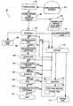
- FIG. 1is a flow diagram illustrating a conventional integrated circuit (IC) device manufacturing process
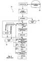
- FIG. 2is a flow diagram illustrating a conventional Chip-On-Board (COB) or flip-chip attached IC manufacturing process
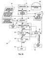
- FIG. 3Ais a flow diagram illustrating an IC device manufacturing process in accordance with the present invention.
- FIG. 3Bis a flow diagram illustrating an assembly portion of the manufacturing process of FIG. 3A in more detail
- FIG. 4Ais a flow diagram illustrating a COB or flip-chip multi-chip module IC manufacturing process in accordance with the present invention.
- FIG. 4Bis a flow diagram illustrating an assembly portion of the manufacturing process of FIG. 4A in more detail.
- an inventive process 30 for manufacturing Dynamic Random Access Memory (DRAM) Integrated Circuit semiconductor devicesbegins with DRAM ICs being fabricated in a fabrication step 32 on the surface of a semiconductor wafer 34 .
- DRAMDynamic Random Access Memory
- SDRAMSynchronous DRAM
- processor ICsSingle In-line Memory Modules (SIMMs), Dual In-line Memory Modules (DIMMs), Rambus In-Line Memory Modules (RIMM), Small Outline Rambus In-Line Memory Modules (SO-RIMM), Personal Computer Memory Format (PCMCIA), Board-Over-Chip type substrate configurations, and other Multi-Chip Modules (MCMs).
- SRAMStatic Random Access Memory
- SDRAMSynchronous DRAM
- processor ICsSingle In-line Memory Modules
- SIMMsSingle In-line Memory Modules
- DIMMsDual In-line Memory Modules
- RIMMRambus In-Line Memory Modules
- SO-RIMMSmall Outline Rambus In-Line Memory Modules
- PCMCIAPersonal Computer Memory Format
- the present inventionwill be described below in the context of a wire bond/lead frame assembly process, either a conventional lead frame or leads-over-chip configuration using adhesive tape on the lead frame or the semiconductor die or non-conductive adhesive on the active surface of the semiconductor die (LOC), the present invention is applicable to any IC assembly process, including, for example, Chip On Board (COB)-either single semiconductor device or the modular form of multiple semiconductor device ICs, Board Over Chip (BOC)-either single semiconductor device or the modular form of multiple semiconductor device ICs, any configuration of substrate and component including Tessera style electrical components (film on elastomer), flip-chip processes (as will be described below with respect to FIGS.
- COBChip On Board
- BOCBoard Over Chip
- TABTape-Automated Bonding
- the DRAM ICsare electronically probed in a probe step 36 to determine whether they are good or bad, and if any DRAM ICs are found to be bad, an attempt is made to repair those ICs by replacing nonfunctional rows or columns in the ICs with spare rows or columns.
- the location of bad DRAM ICs on a wafer 34along with the location of any good DRAM ICs on the wafer 34 , is stored in a computer in an electronic wafer map in association with data identifying spare rows and columns still available in each of the DRAM ICs after any repairs performed at the probe step 36 .
- the stored datamay alternatively identify spare rows and columns used in each of the DRAM ICs to effect repairs at the probe step 36 .
- DRAM ICs fabricated on the wafers 34are programmed in the manner described above with a fuse identification (ID) unique to each IC.
- IDa fuse identification
- the fuse ID for each DRAM ICis then stored in association with the repair data 38 for that IC.
- the fuse IDmay identify, for example, a wafer lot ID, the week the DRAM ICs were fabricated, a wafer ID, a die location on the wafer, and a fabrication facility ID.
- the availability of spare rows or columns for effecting post-probe repairs in a particular DRAM ICcan be determined by using the fuse ID of the IC to access the stored repair data 38 for the IC, as will be described in more detail below.
- DRAM ICsand other ICs having any ID code, such as a dot code, bar code, or any suitable type marking code on the ICs, including those having fuse IDs. It will also be understood that the ICs may be programmed with their fuse IDs at steps in the manufacturing process 30 other than the probe step 36 .
- DRAM ICsAfter being probed and, if necessary, repaired, DRAM ICs enter an assembly process 40 in which good ICs are assembled into IC devices, as will be described in more detail below with respect to FIG. 3B , while bad ICs are discarded in a scrap bin 42 .
- DRAM ICs 44that have been diverted from COB and flip-chip manufacturing process flows enter the assembly process 40 and are also assembled into IC devices.
- the DRAM ICs 44are diverted from the COB and flip-chip process flows because so many of their spare rows and columns have been used at probe to effect repairs in the DRAM ICs 44 that the DRAM ICs 44 fall below a minimum threshold level of repairability, as will be described in more detail below with respect to FIGS. 4A and 4B .
- discrete DRAM IC devicesare tested in an opens/shorts test 46 .
- the fuse ID of the DRAM IC in each IC deviceis automatically read and correlated with the repair data 38 produced in the manufacturing process 30 or repair data 48 produced in a COB or flip-chip process flow as described below. It should be understood that although the fuse IDs of DRAM ICs in the process 30 are typically read electronically, they may also be read optically if the fuse IDs consist of “blown” laser fuses that are optically accessible. It should also be understood that the fuse IDs of DRAM ICs may be read at steps in the process 30 other than the opens/shorts test 46 .
- DRAM IC devices that pass the opens/shorts test 46proceed on through the process 30 to various burn-in and test procedures 50 and 52 where they are tested for functionality, operability, and reliability, and DRAM IC devices that pass these burn-in and test procedures 50 and 52 are shipped 54 to customers.
- DRAM IC devices that fail any of the opens/shorts, burn-in, and test procedures 46 , 50 , and 52proceed to repair 56 .
- Those DRAM IC devices that do not have enough available spare rows and columns to effect repairs, and thus are unrepairable,are identified as such when their repair data 38 and 48 is accessed at the opens/shorts test 46 , and these devices proceed directly to rework or a scrap bin 58 without the need to query them.
- DRAM IC devices that are identified by their repair data 38 and 48 as being repairableare repaired, typically by replacing nonfunctional rows and columns with spare rows and columns in the same manner as described above. After being repaired, these DRAM IC devices then reenter the manufacturing process 30 just prior to the opens/shorts, burn-in, or test procedures 46 , 50 , and 52 they failed.
- the assembly process 40 of FIG. 3Ais shown in more detail in FIG. 3B .
- probed and repaired semiconductor wafersenter a wafer saw step 60 and are mounted on an adhesive film.
- the filmmay be any one of a wide variety of adhesive films used for this purpose, including, for example, a special high-adhesion U.V. film.
- DRAM ICsare then sawed from their wafer into discrete IC dice using high-speed precision dicing equipment.
- DRAM IC dice that are mounted on the special high-adhesion U.V. filmare then exposed to U.V. light in an optional U.V. exposure step 62 to loosen the grip of the film on the dice.
- DRAM IC dice identified as good by their electronic wafer mapare then each picked by automated equipment from their sawed wafer and its associated film in a die attach step 64 and placed on an epoxy-coated bonding site of one lead frame in a strip of interconnected lead frames, while DRAM IC dice identified as bad are discarded into the scrap bin 42 .
- DRAM ICs 44 that have been diverted from COB and flip-chip manufacturing process flowsenter the assembly process 40 and are also placed on an adhesive-coated bonding site of one lead frame in a lead frame strip. These diverted DRAM ICs 44 will be described in more detail below with respect to FIGS. 4A and 4B .
- the adhesive attaching the good DRAM IC dice to their lead framesis then cured, if required, in a cure step 66 , and the attached dice are wire bonded to their lead frames using high-speed bonding equipment in a wire bond step 68 .
- DRAM IC dice and their lead framescontinue the assembly process 40 by being formed into DRAM IC packages using a hot thermosetting plastic encapsulant injected into a mold in an overmold step 70 .
- DRAM IC packagesare then cured in a further cure step 72 to set their plastic encapsulant.
- leads of the lead frames projecting from the packagesmay be dipped in a cleansing chemical bath in a de-flash process 74 and then may be electroplated with a lead/tin finish if they are not already plated.
- connections between the lead frames of different DRAM IC packagesare then cut in a singulate step 76 to separate the packages into discrete DRAM IC devices.
- an inventive COB or flip-chip process 80 for manufacturing DRAM SIMMsbegins with DRAM ICs being fabricated in a fabrication step 82 on the surface of a semiconductor wafer 84 . It will be understood by those having skill in the field of this invention that the present invention is applicable to any IC devices, including SRAM ICs, SDRAM ICs, processor ICs, and modules using such IC devices, such as DIMMs, RIMMs, SO-RIMMS, PCMCIAs, COBs, BOCs, and other MCMs.
- the present inventionis applicable to any IC assembly process, including, for example, Tape-Automated Bonding (TAB) processes, wafer scale processes including packaging, partial wafer scale processes including packaging, etc. It should be further understood that the present invention relates to any type IC that has been singulated by any type singulation process or apparatus, such as wafer saw singulation, laser apparatus singulation, laser/water apparatus singulation (cool laser singulation), water jet apparatus singulation, etc.
- TABTape-Automated Bonding
- the DRAM ICsare electronically probed in a probe step 86 to determine whether they are good or bad, and if any DRAM ICs are found to be bad, an attempt is made to repair the ICs by replacing nonfunctional rows or columns in the ICs with spare rows or columns.
- the locations of bad DRAM ICs on a wafer 84along with the locations of any good DRAM ICs on the wafer 84 , are stored in a computer in an electronic wafer map in association with repair data 48 identifying spare rows and columns still available in each of the DRAM ICs after any repairs performed at the probe step 86 .
- DRAM ICs fabricated on the wafers 84are programmed in the manner described above with a fuse identification (ID) unique to each IC.
- IDa fuse identification
- the fuse ID for each DRAM ICis then stored in association with the repair data 48 for that IC.
- the fuse IDmay identify, for example, a wafer lot ID, the week the DRAM ICs were fabricated, a wafer ID, a die location on the wafer, and a fabrication facility ID.
- the present inventionincludes within its scope ICs having any ID code, including those having fuse IDs. It will also be understood that the ICs may be programmed with their fuse IDs at steps in the manufacturing process 80 other than the probe step 86 .
- DRAM ICsAfter being probed and, if necessary, repaired, DRAM ICs enter an assembly process 90 in which good ICs are assembled into panels of physically interconnected DRAM SIMMs, as will be described in more detail below with respect to FIG. 4B , while bad ICs are discarded in a scrap bin 92 .
- DRAM ICs 44in which so many spare rows and columns have been used at the probe step 86 to effect repairs that the ICs 44 fall below a minimum threshold of repairability are diverted from the COB or flip-chip process 80 for use in the standard assembly process 40 of FIGS. 3A and 3B .
- a “minimum threshold of repairability”can be set at any level, it might be set, for example, at a level at which statistically the available spare rows and columns in a DRAM IC would only be able to effect repairs in an unacceptably low percentage (e.g., 50%) of cases of failures.
- the diverted DRAM ICs 44typically include those ICs that have exhausted their spare rows and columns in repairs at the probe step 86 and those ICs that have some, but not enough, spare rows and columns left after being repaired at the probe step 86 .
- the present inventionthus prevents DRAM ICs that would be repairable in few or none of the possible cases of failure from being assembled into DRAM SIMMs and other MCMs, and thus prevents the waste of time and resources associated with scrapping or reworking MCMs into which such ICs have traditionally been assembled.
- each DRAM IC in each DRAM SIMMis automatically read and correlated with the repair data 48 . It should be understood that although the fuse IDs of DRAM ICs in the process 80 are typically read electronically, they may also be read optically if the fuse IDs consist of “blown” laser fuses that are optically accessible. It should also be understood that the fuse IDs of DRAM ICs may be read at steps in the process 80 other than the opens/shorts test 96 .
- panels of DRAM SIMMs having COB IC dice that pass the opens/shorts test 96proceed to an encapsulation step 98 so the dice can be encapsulated using an overmold, hard cover, or glob top.
- panels of DRAM SIMMs having flip-chip IC dice that pass the opens/shorts test 96may have their dice encapsulated at the encapsulation step 98 using an underfill followed by an overmold, hard cover, or glob top.
- the flip-chip IC dicemay be encapsulated after burn-in and test procedures. The disposition of panels of DRAM SIMMs having IC dice that fail the opens/shorts test will be described in more detail below.
- Panels of DRAM SIMMs having either COB or flip-chip IC diceare then singulated into discrete DRAM SIMMs at a singulation step 100 by, for example, a water jet or a shear press.
- This singulation step 100may, for example, divide a “ten” panel of ten physically attached DRAM SIMMs into ten discrete DRAM SIMMs.
- DRAM SIMMs having encapsulated IC diceare tested again in an additional opens/shorts test 102 to check for problems caused by the encapsulation step 98 .
- DRAM SIMMs having encapsulated dice that pass this additional opens/shorts test 102then proceed on in the manufacturing process 80 to burn-in testing 104 and back-end testing 106 .
- the disposition of those DRAM SIMMs having encapsulated IC dice that fail the additional opens/shorts test 102will be described in more detail below.
- the fuse IDs of the IC dice in the DRAM SIMMsmay also be automatically read at this additional opens/shorts test 102 .
- DRAM SIMMs having unencapsulated flip-chip IC dice that pass the procedures 104 and 106proceed on in the process 80 to an optional cover step 108 so their dice may be covered with an overmold, hardcover, or glob top. Dice covered in this manner are then checked in a further opens/shorts test 108 for problems caused by their being covered, and DRAM SIMMs having dice that pass this further test are then typically shipped in a shipping step 110 to customers. DRAM SIMMs having encapsulated IC dice that pass the burn-in and test procedures 104 and 106 skip this covering and final opens/shorts test step 108 and proceed to the shipping step 110 .
- the fuse IDs of the IC dice in the DRAM SIMMs tested at any of the burn-in, back-end test, and opens/shorts test procedures 104 , 106 , and 108may be automatically read at any one or all of those tests.
- DRAM SIMMs having IC dice that fail any of the opens/shorts, burn-in, and test procedures 96 , 102 , 104 , 106 and 108proceed to repair 112 .
- Those DRAM SIMMs having DRAM IC dice that do not have enough available spare rows and columns to effect repairs, and thus are unrepairable,are identified as such when their repair data 48 is accessed at any one of the opens/shorts, burn-in, and back-end tests 96 , 102 , 104 , 106 , and 108 , and these SIMMs proceed directly to rework (described below) or a scrap bin 114 without the need to query them.
- DRAM SIMMs having DRAM IC dice identified by their repair data 48 as being repairableare repaired, typically by replacing nonfunctional rows and columns with spare rows and columns in the same manner as described above. After being repaired, these DRAM SIMMs then reenter the manufacturing process 80 just prior to the opens/shorts, burn-in, or test procedures 96 , 102 , 104 , 106 or 108 they failed.
- DRAM SIMMs that are reworkable by replacing one or more non-functioning IC diceproceed through a Known Good Die (KGD) process in which a DRAM KGD (i.e., a burned-in, fully tested, fully functional DRAM) replaces the non-functioning IC dice on the SIMMs in a replacement step 116 .
- KGDKnown Good Die
- the KGD repairsare then tested in a repair step 118 , and if the repairs are successful, the repaired DRAM SIMMs reenter the manufacturing process 80 just prior to the back-end test procedures 106 . If the repairs are not successful, the DRAM SIMMs may return to the repair step 112 to be reworked again or, if they are not reworkable, to be scrapped in the scrap bin 114 .
- the assembly process 90 of FIG. 4Ais shown in more detail in FIG. 4B .
- probed and repaired semiconductor wafersenter a wafer saw step 120 and are mounted on an adhesive film.
- the filmmay be any one of a wide variety of adhesive films used for this purpose, including, for example, a special high-adhesion U.V. film.
- DRAM ICsare then sawed from their wafer into discrete DRAM IC dice using high-speed precision dicing equipment.
- DRAM IC dice that are mounted on the special high-adhesion U.V. filmare then exposed to U.V. light in an optional U.V. exposure step 122 to loosen the grip of the film on the dice.
- IC dice identified as good by their electronic wafer mapare then each picked by automated equipment from their sawed wafer and its associated film at an attachment step 124 .
- the assembly process 90is a flip-chip process, multiple picked dice are then flipped and directly attached at their active, front side surfaces to a panel of PCBs or other substrates to form, for example, DRAM SIMMs.
- the assembly process 90is a COB process, multiple picked dice are directly attached at their inactive, back side surfaces to an adhesive-coated bonding site of a panel of PCBs or other substrates to form, for example, DRAM SIMMs.
- DRAM ICs identified as badare discarded into the scrap bin 92 , while DRAM ICs 44 that have used so many of their spare rows and columns in repairs at the probe step 86 that they fall below the minimum threshold of repairability are diverted to the standard assembly process 40 of FIGS. 3A and 3B .
- Panels of DRAM SIMMsare then cured at a cure step 126 . If the assembly process 90 is a COB process, the panels may be plasma cleaned in an optional plasma cleaning step 128 , if necessary, and the COB IC dice are then wire bonded at a wire bond step 130 to their DRAM SIMMs using high-speed bonding equipment. DRAM SIMMs then proceed to the opens/shorts test 96 described above with respect to FIG. 4A .
Landscapes
- Engineering & Computer Science (AREA)
- Theoretical Computer Science (AREA)
- Physics & Mathematics (AREA)
- General Physics & Mathematics (AREA)
- Quality & Reliability (AREA)
- General Engineering & Computer Science (AREA)
- Testing Or Measuring Of Semiconductors Or The Like (AREA)
Abstract
Description
- This application is a continuation of application Ser. No. 09/653,272, filed Aug. 31, 2000, which issues as U.S. Pat. No. 7,120,513 on Oct. 10, 2006, which application is a continuation-in-part of application Ser. No. 09/292,655, filed Apr. 15, 1999, now U.S. Pat. No. 6,363,295, issued Mar. 26, 2002, which is a continuation of application Ser. No. 08/871,015, filed Jun. 6, 1997, now U.S. Pat. No. 5,907,492, issued May 25, 1999.
- This application is related to: an application having Ser. No. 08/591,238, filed Jan. 17, 1996, entitled “METHOD AND APPARATUS [sic] FOR STORAGE OF TEST RESULTS WITHIN AN INTEGRATED CIRCUIT,” abandoned in favor of a continuation-in-part application filed Feb. 27, 1998, having Ser. No. 09/032,417, and entitled “METHOD AND APPARATUS [sic] FOR STORAGE OF TEST RESULTS WITHIN AN INTEGRATED CIRCUIT,” now U.S. Pat. No. 6,194,738, issued Feb. 27, 2001; an application having Ser. No. 08/664,109, filed Jun. 13, 1996, entitled “A STRUCTURE AND A METHOD FOR STORING INFORMATION IN A SEMICONDUCTOR DEVICE,” now U.S. Pat. No. 5,895,962, issued Apr. 20, 1999; an application filed Jan. 17, 1997 having Ser. No. 08/785,353 and entitled “METHOD FOR SORTING INTEGRATED CIRCUIT DEVICES,” now U.S. Pat. No. 5,927,512, issued Jul. 27, 1999; an application filed Feb. 17, 1997 having Ser. No. 08/801,565 and entitled “METHOD OF SORTING A GROUP OF INTEGRATED CIRCUIT DEVICES FOR THOSE DEVICES REQUIRING SPECIAL TESTING,” now U.S. Pat. No. 5,844,803, issued Dec. 1, 1998; an application filed Feb. 26, 1997 having Ser. No. 08/806,442 and entitled “METHOD IN AN INTEGRATED CIRCUIT (IC) MANUFACTURING PROCESS FOR IDENTIFYING AND RE-DIRECTING ICS MIS-PROCESSED DURING THEIR MANUFACTURE,” now U.S. Pat. No. 5,915,231, issued Jun. 22, 1999; and an application filed Mar. 24, 1997 having Ser. No. 08/822,731 and entitled “METHOD FOR CONTINUOUS, NON LOT-BASED INTEGRATED CIRCUIT MANUFACTURING,” now U.S. Pat. No. 5,856,923, issued Jan. 5, 1999.
- 1. Field of the Invention
- The present invention relates in general to integrated circuit semiconductor device (IC) manufacturing. More specifically, it relates to methods in IC manufacturing processes for using data regarding manufacturing procedures ICs have undergone, such as repair procedures, to select procedures the ICs will undergo, such as additional repair procedures.
- 2. State of the Art
- As shown in
FIG. 1 , atypical process 10 for manufacturing very small electronic semiconductor device circuits referred to as “Integrated Circuits” (ICs) begins with the ICs being formed or “fabricated” on the surface of awafer 12 of semiconductor material, such as silicon. Once fabricated, ICs are electronically probed to determine whether they are functional (i.e., “good”) or nonfunctional (i.e., “bad”). If any ICs are found to be bad, an attempt is made to repair those ICs by replacing nonfunctional circuit elements in the ICs with spare circuit elements. For example, Dynamic Random Access Memory (DRAM) ICs are typically repaired by replacing nonfunctional rows or columns of memory cells in the ICs with spare rows or columns. - These repairs are not always successful, because the number of spare circuit elements on an IC may be exhausted before all nonfunctional circuit elements on the IC are replaced, and because some circuit elements on ICs have no spares to replace them. As a result, a number of bad ICs typically remain on a
wafer 12 even after attempts are made to repair the ICs. The location of bad ICs on awafer 12, along with the location of any good ICs on thewafer 12, is typically stored in a computer database commonly referred to as a “wafer map.” - After being probed and, if necessary, repaired, ICs begin an assembly process with their
wafer 12 being mounted on an adhesive film. In some instances, the film is a special high-adhesion Ultraviolet (U.V.) film. Without cutting the adhesive film, ICs are sawed from theirwafer 12 into discrete IC dice or “chips” using high-speed precision dicing equipment. IC dice mounted on U.V. film are then exposed to U.V. light to loosen the grip of the film on the dice. IC dice identified as good by their wafer map are then each “picked” by automated equipment from their sawedwafer 12 and its associated film and “placed” on an epoxy-coated bonding site of one lead frame in a strip of interconnected lead frames, while IC dice identified as bad are discarded into ascrap bin 14. The epoxy attaching the good IC dice to their lead frames is then cured, and the attached dice are wire bonded to their lead frames using high-speed bonding equipment. - Once wire bonded, IC dice and their associated lead frames are formed into IC packages using a hot thermosetting plastic encapsulant injected into a mold. IC packages are then cured to set their plastic encapsulant. After encapsulation and curing, leads of the lead frames projecting from the packages are dipped in a cleansing chemical bath in a process referred to as “de-flash” and then electroplated with a lead/tin finish. Connections between lead frames in lead frame strips are then cut to “singulate” IC packages into discrete IC devices.
- After assembly, discrete IC devices are tested in a simple electronic test referred to as an “opens/shorts” test, which checks for “opens” (i.e., no connection) within the devices where connections should exist and “shorts” (i.e., a connection) where connections should not exist. Devices that pass the opens/shorts test proceed on through the
process 10 to various burn-in and test procedures where they are tested for functionality, operability, and reliability, and devices that pass these burn-in and test procedures are then typically shipped to customers. - IC devices that fail any of the opens/shorts, burn-in, and test procedures are checked to determine whether they are repairable. This “check” typically includes an electronic “querying” of a device to determine whether enough spare circuit elements remain in the device to effect necessary repairs. Devices determined to be unrepairable are scrapped in a
scrap bin 16, while devices that are repairable are repaired, typically by replacing nonfunctional circuit elements in the devices with spare circuit elements in the same manner as described above. After being repaired, these devices then reenter themanufacturing process 10 just prior to the opens/shorts, burn-in, or test procedures they failed. - Electronic querying of IC devices to determine whether spare circuit elements are available to effect repairs increases the time required to move the devices through the
manufacturing process 10 and places an additional burden on expensive testing resources. While the extra time added by querying one IC device may be insignificant, the time required to query thousands and thousands of IC devices adds up and can result in a significant reduction in the number of IC devices completing themanufacturing process 10 in a given amount of time. Therefore, there is a need in the art for a method of determining whether enough spare circuit elements are available in an IC device to effect repairs without having to query the device. - Similarly, as shown in
FIG. 2 , atypical process 20 for manufacturing so-called “flip-chip” and “Chip-On-Board” (COB) Multi-Chip Modules (MCMs), in which multiple IC dice are typically attached directly to a substrate, such as a printed circuit board (PCB), begins with ICs being fabricated on the surface of asemiconductor wafer 22 in the same manner as described above. Once fabricated, ICs are electronically probed to determine whether they are good or bad, and if any ICs are found to be bad, an attempt is made to repair those ICs (i.e., make them good ICs) by replacing nonfunctional circuit elements in the ICs with spare circuit elements. The locations of good and bad ICs on awafer 22 are then typically stored in an electronic wafer map. - After being probed and, if necessary, repaired, ICs begin an assembly process with their
wafer 22 being mounted on an adhesive film. Without cutting this film, ICs are then sawed from theirwafer 22 into discrete IC dice using high-speed precision dicing equipment. IC dice that are mounted on the special high-adhesion U.V. film described above are then exposed to U.V. light to loosen the grip of the film on the dice. - IC dice identified as good by their electronic wafer map are then each picked by automated equipment from their sawed
wafer 22 and its associated film, typically for attachment to a substrate in a panel of multiple substrates, such as a panel of interconnected PCBs. If the assembly process is a flip-chip process, picked dice are then flipped and directly attached at their active, front side surfaces to substrates to form MCMs. If the assembly process is a COB process, picked dice are directly attached at their inactive, back side surfaces to adhesive-coated bonding sites of substrates to form MCMs. IC dice identified as bad are discarded into ascrap bin 24. - Panels of MCMs are then cured. If the assembly process is a COB process, the MCMs may be plasma cleaned, if necessary, and the COB IC dice are then wire bonded to their substrates using high-speed bonding equipment.
- After assembly, panels of MCMs are tested in an opens/shorts test. Panels having COB IC dice that pass the opens/shorts test proceed on through the
manufacturing process 20 so the dice can be encapsulated using an overmold, hard cover, or so-called “glob” top, while panels having flip-chip IC dice that pass the opens/shorts test may have their dice encapsulated using an underfill followed by an overmold, hard cover, or glob top. As will be described in more detail below, alternatively, flip-chip IC dice may be encapsulated after burn-in and test procedures. The disposition of panels of MCMs having COB and flip-chip attached IC dice that fail the opens/shorts test will be described in more detail below. - Panels of MCMs having both COB and flip-chip IC dice, including those panels having flip-chip IC dice that were not encapsulated, are then singulated into discrete MCMs, typically by a shear press or router. After singulation, those MCMs having encapsulated IC dice have their dice tested again in an additional opens/shorts test to check for problems caused by the encapsulation. MCMs having encapsulated dice that pass this additional opens/shorts test, as well as MCMs having dice that were not encapsulated, then proceed on in the
manufacturing process 20 to various burn-in and test procedures. The disposition of any MCMs having encapsulated dice that fail the additional opens/shorts test will be described in more detail below. - After the burn-in and test procedures, MCMs having unencapsulated flip-chip IC dice that pass the procedures proceed on in the
process 20 so their dice may be covered with an overmold, hardcover, or glob top. Dice covered in this manner are then checked in a further opens/shorts test for problems caused by their being covered, and MCMs having dice that pass this further test are then typically shipped to customers. MCMs having encapsulated IC dice that pass the burn-in and test procedures skip this final opens/shorts test and typically proceed to shipping. - MCMs having attached IC dice that fail any of the opens/shorts, burn-in, and test procedures are checked to determine whether their associated IC dice are repairable. This “check” typically includes an electronic querying of the IC dice to determine whether enough spare circuit elements remain in the dice for effecting repairs. MCMs determined to have unrepairable IC dice are then either reworked using replacement IC dice in an expensive and time-consuming procedure or scrapped in a
scrap bin 26, while MCMs having IC dice that are repairable are repaired, typically by replacing nonfunctional circuit elements in the IC dice with spare circuit elements. After being repaired, these MCMs then reenter themanufacturing process 20 just prior to the opens/shorts, burn-in, or test procedures they failed. - As discussed above, electronic querying of IC dice to determine whether spare circuit elements are available to effect repairs increases the time required to move MCMs through the
manufacturing process 20 and places an additional burden on expensive testing resources. Also, IC dice that require repair, and are found to be unrepairable only after the assembly process, waste assembly time, materials, and resources and necessitate the scrapping or reworking of MCMs that may contain many functional dice. It is desirable, then, to have an IC manufacturing method for identifying unrepairable IC dice so they may be kept out of COB, flip-chip and other MCM assembly processes. - As described in U.S. Pat. Nos. 5,301,143, 5,294,812, and 5,103,166, some methods have been devised to electronically identify IC dice. Such methods take place “off” the manufacturing line, and involve the use of electrically retrievable identification (ID) codes, such as so-called “fuse IDs,” programmed into individual IC dice to identify the dice. The programming of a fuse ID typically involves selectively blowing an arrangement of fuses or anti-fuses in an IC die using electric current or a laser so that when the fuses or anti-fuses are accessed, they output a preprogrammed ID code. Unfortunately, none of these methods addresses the problem of identifying unrepairable IC dice “on” a manufacturing line.
- The present invention provides a method in an integrated circuit (IC) manufacturing process for using data regarding manufacturing procedures ICs have undergone, such as repair procedures at probe, to select manufacturing procedures the ICs will undergo, such as additional repair procedures during back-end testing. The ICs are each programmed with a substantially unique identification (ID) code, such as a fuse ID.
- The method includes storing data in association with the ID codes of the ICs that identifies manufacturing procedures the ICs have undergone. This data may identify spare circuitry already used to repair the ICs at probe, for example, or spare circuitry available to repair the ICs. The ID codes of the ICs are automatically read, for example, at an opens/shorts test during the manufacturing process. The data stored in association with the ID codes is then accessed, and manufacturing procedures the ICs will undergo, such as additional repair procedures during back-end testing, are selected in accordance with the accessed data. Thus, for example, the accessed data may indicate that insufficient spare circuitry is available on an IC to effect repairs, so the IC can proceed directly to a scrap bin without being “queried” to determine the availability of spare circuitry, as is traditionally necessary. The present invention thus eliminates the time-wasting conventional process of querying ICs prior to repair or scrapping.
- Further embodiments include methods of manufacturing IC devices and Multi-Chip Modules (MCMs) which incorporate the method described above.
- In an additional embodiment, a method in an MCM manufacturing process for diverting good but unrepairable IC dice from the process includes storing data in association with ID codes, such as fuse IDs, of the ICs that identifies ICs that are a) good and repairable, b) good but unrepairable, and c) bad. In the inventive method, the ID codes of the ICs are automatically read, and the data stored in association with the ID codes is accessed. ICs identified as good but unrepairable by the accessed data are diverted to other IC manufacturing processes, while ICs identified as bad are discarded, and ICs identified as good and repairable are assembled into MCMs.
- The present invention thus prevents ICs that are unrepairable from being assembled into MCMs, such as Single In-Line Memory Modules (SIMMs), and thus prevents the reworking or scrapping of MCMs into which unrepairable ICs have been assembled.
FIG. 1 is a flow diagram illustrating a conventional integrated circuit (IC) device manufacturing process;FIG. 2 is a flow diagram illustrating a conventional Chip-On-Board (COB) or flip-chip attached IC manufacturing process;FIG. 3A is a flow diagram illustrating an IC device manufacturing process in accordance with the present invention;FIG. 3B is a flow diagram illustrating an assembly portion of the manufacturing process ofFIG. 3A in more detail;FIG. 4A is a flow diagram illustrating a COB or flip-chip multi-chip module IC manufacturing process in accordance with the present invention; andFIG. 4B is a flow diagram illustrating an assembly portion of the manufacturing process ofFIG. 4A in more detail.- As shown in
FIG. 3A , aninventive process 30 for manufacturing Dynamic Random Access Memory (DRAM) Integrated Circuit semiconductor devices (ICs) begins with DRAM ICs being fabricated in afabrication step 32 on the surface of asemiconductor wafer 34. It will be understood by those having skill in the field of this invention that the present invention is applicable to any IC devices, including Static Random Access Memory (SRAM) ICs, Synchronous DRAM (SDRAM) ICs, processor ICs, Single In-line Memory Modules (SIMMs), Dual In-line Memory Modules (DIMMs), Rambus In-Line Memory Modules (RIMM), Small Outline Rambus In-Line Memory Modules (SO-RIMM), Personal Computer Memory Format (PCMCIA), Board-Over-Chip type substrate configurations, and other Multi-Chip Modules (MCMs). It will also be understood that although the present invention will be described below in the context of a wire bond/lead frame assembly process, either a conventional lead frame or leads-over-chip configuration using adhesive tape on the lead frame or the semiconductor die or non-conductive adhesive on the active surface of the semiconductor die (LOC), the present invention is applicable to any IC assembly process, including, for example, Chip On Board (COB)-either single semiconductor device or the modular form of multiple semiconductor device ICs, Board Over Chip (BOC)-either single semiconductor device or the modular form of multiple semiconductor device ICs, any configuration of substrate and component including Tessera style electrical components (film on elastomer), flip-chip processes (as will be described below with respect toFIGS. 4A and 4B ), Tape-Automated Bonding (TAB) processes, and wafer scale semiconductor device packages or packaging, either the entire wafer as a whole, multiple semiconductor devices as portions of the wafer which are singulated and packaged, or the singulation of the semiconductor devices on the wafer which are later packaged and/or mounted. - Once fabricated, the DRAM ICs are electronically probed in a
probe step 36 to determine whether they are good or bad, and if any DRAM ICs are found to be bad, an attempt is made to repair those ICs by replacing nonfunctional rows or columns in the ICs with spare rows or columns. The location of bad DRAM ICs on awafer 34, along with the location of any good DRAM ICs on thewafer 34, is stored in a computer in an electronic wafer map in association with data identifying spare rows and columns still available in each of the DRAM ICs after any repairs performed at theprobe step 36. Of course, it will be understood that the stored data may alternatively identify spare rows and columns used in each of the DRAM ICs to effect repairs at theprobe step 36. - During the
probe step 36, DRAM ICs fabricated on thewafers 34 are programmed in the manner described above with a fuse identification (ID) unique to each IC. The fuse ID for each DRAM IC is then stored in association with therepair data 38 for that IC. The fuse ID may identify, for example, a wafer lot ID, the week the DRAM ICs were fabricated, a wafer ID, a die location on the wafer, and a fabrication facility ID. As a result of storing the fuse ID for each DRAM IC in association with therepair data 38, the availability of spare rows or columns for effecting post-probe repairs in a particular DRAM IC can be determined by using the fuse ID of the IC to access the storedrepair data 38 for the IC, as will be described in more detail below. - It will be understood, of course, that the present invention includes within its scope DRAM ICs and other ICs having any ID code, such as a dot code, bar code, or any suitable type marking code on the ICs, including those having fuse IDs. It will also be understood that the ICs may be programmed with their fuse IDs at steps in the
manufacturing process 30 other than theprobe step 36. - After being probed and, if necessary, repaired, DRAM ICs enter an
assembly process 40 in which good ICs are assembled into IC devices, as will be described in more detail below with respect toFIG. 3B , while bad ICs are discarded in ascrap bin 42. In addition,DRAM ICs 44 that have been diverted from COB and flip-chip manufacturing process flows enter theassembly process 40 and are also assembled into IC devices. TheDRAM ICs 44 are diverted from the COB and flip-chip process flows because so many of their spare rows and columns have been used at probe to effect repairs in theDRAM ICs 44 that theDRAM ICs 44 fall below a minimum threshold level of repairability, as will be described in more detail below with respect toFIGS. 4A and 4B . - After the
assembly process 40, discrete DRAM IC devices are tested in an opens/shorts test 46. There, the fuse ID of the DRAM IC in each IC device is automatically read and correlated with therepair data 38 produced in themanufacturing process 30 orrepair data 48 produced in a COB or flip-chip process flow as described below. It should be understood that although the fuse IDs of DRAM ICs in theprocess 30 are typically read electronically, they may also be read optically if the fuse IDs consist of “blown” laser fuses that are optically accessible. It should also be understood that the fuse IDs of DRAM ICs may be read at steps in theprocess 30 other than the opens/shorts test 46. - DRAM IC devices that pass the opens/
shorts test 46 proceed on through theprocess 30 to various burn-in andtest procedures test procedures - DRAM IC devices that fail any of the opens/shorts, burn-in, and
test procedures repair data shorts test 46, and these devices proceed directly to rework or ascrap bin 58 without the need to query them. Of course, DRAM IC devices that are identified by theirrepair data manufacturing process 30 just prior to the opens/shorts, burn-in, ortest procedures - It should be understood, of course, that the present invention is applicable to situations in a wide variety of IC manufacturing processes in which data regarding manufacturing procedures the ICs have undergone, such as repair procedures at probe, may be accessed through the use of fuse IDs and other ID codes to determine procedures the ICs should undergo, such as post-probe repairs.
- As stated above, the
assembly process 40 ofFIG. 3A is shown in more detail inFIG. 3B . In theprocess 40, probed and repaired semiconductor wafers enter a wafer sawstep 60 and are mounted on an adhesive film. The film may be any one of a wide variety of adhesive films used for this purpose, including, for example, a special high-adhesion U.V. film. Without cutting the film, DRAM ICs are then sawed from their wafer into discrete IC dice using high-speed precision dicing equipment. DRAM IC dice that are mounted on the special high-adhesion U.V. film are then exposed to U.V. light in an optional U.V.exposure step 62 to loosen the grip of the film on the dice. - DRAM IC dice identified as good by their electronic wafer map are then each picked by automated equipment from their sawed wafer and its associated film in a die attach
step 64 and placed on an epoxy-coated bonding site of one lead frame in a strip of interconnected lead frames, while DRAM IC dice identified as bad are discarded into thescrap bin 42. In addition,DRAM ICs 44 that have been diverted from COB and flip-chip manufacturing process flows enter theassembly process 40 and are also placed on an adhesive-coated bonding site of one lead frame in a lead frame strip. These divertedDRAM ICs 44 will be described in more detail below with respect toFIGS. 4A and 4B . The adhesive attaching the good DRAM IC dice to their lead frames is then cured, if required, in acure step 66, and the attached dice are wire bonded to their lead frames using high-speed bonding equipment in awire bond step 68. - Once wire bonded, DRAM IC dice and their lead frames continue the
assembly process 40 by being formed into DRAM IC packages using a hot thermosetting plastic encapsulant injected into a mold in anovermold step 70. DRAM IC packages are then cured in afurther cure step 72 to set their plastic encapsulant. After encapsulation and curing, leads of the lead frames projecting from the packages may be dipped in a cleansing chemical bath in ade-flash process 74 and then may be electroplated with a lead/tin finish if they are not already plated. Finally, connections between the lead frames of different DRAM IC packages are then cut in asingulate step 76 to separate the packages into discrete DRAM IC devices. - In another embodiment of the present invention shown in
FIG. 4A , an inventive COB or flip-chip process 80 for manufacturing DRAM SIMMs begins with DRAM ICs being fabricated in afabrication step 82 on the surface of asemiconductor wafer 84. It will be understood by those having skill in the field of this invention that the present invention is applicable to any IC devices, including SRAM ICs, SDRAM ICs, processor ICs, and modules using such IC devices, such as DIMMs, RIMMs, SO-RIMMS, PCMCIAs, COBs, BOCs, and other MCMs. It will also be understood that although the present invention will be described below in the context of both a COB process and a flip-chip assembly process, the present invention is applicable to any IC assembly process, including, for example, Tape-Automated Bonding (TAB) processes, wafer scale processes including packaging, partial wafer scale processes including packaging, etc. It should be further understood that the present invention relates to any type IC that has been singulated by any type singulation process or apparatus, such as wafer saw singulation, laser apparatus singulation, laser/water apparatus singulation (cool laser singulation), water jet apparatus singulation, etc. - Once fabricated, the DRAM ICs are electronically probed in a
probe step 86 to determine whether they are good or bad, and if any DRAM ICs are found to be bad, an attempt is made to repair the ICs by replacing nonfunctional rows or columns in the ICs with spare rows or columns. The locations of bad DRAM ICs on awafer 84, along with the locations of any good DRAM ICs on thewafer 84, are stored in a computer in an electronic wafer map in association withrepair data 48 identifying spare rows and columns still available in each of the DRAM ICs after any repairs performed at theprobe step 86. - During the
probe step 86, DRAM ICs fabricated on thewafers 84 are programmed in the manner described above with a fuse identification (ID) unique to each IC. The fuse ID for each DRAM IC is then stored in association with therepair data 48 for that IC. The fuse ID may identify, for example, a wafer lot ID, the week the DRAM ICs were fabricated, a wafer ID, a die location on the wafer, and a fabrication facility ID. - It will be understood, of course, that the present invention includes within its scope ICs having any ID code, including those having fuse IDs. It will also be understood that the ICs may be programmed with their fuse IDs at steps in the
manufacturing process 80 other than theprobe step 86. - After being probed and, if necessary, repaired, DRAM ICs enter an
assembly process 90 in which good ICs are assembled into panels of physically interconnected DRAM SIMMs, as will be described in more detail below with respect toFIG. 4B , while bad ICs are discarded in ascrap bin 92. In addition,DRAM ICs 44 in which so many spare rows and columns have been used at theprobe step 86 to effect repairs that theICs 44 fall below a minimum threshold of repairability are diverted from the COB or flip-chip process 80 for use in thestandard assembly process 40 ofFIGS. 3A and 3B . Although a “minimum threshold of repairability” can be set at any level, it might be set, for example, at a level at which statistically the available spare rows and columns in a DRAM IC would only be able to effect repairs in an unacceptably low percentage (e.g., 50%) of cases of failures. Thus, the divertedDRAM ICs 44 typically include those ICs that have exhausted their spare rows and columns in repairs at theprobe step 86 and those ICs that have some, but not enough, spare rows and columns left after being repaired at theprobe step 86. - The present invention thus prevents DRAM ICs that would be repairable in few or none of the possible cases of failure from being assembled into DRAM SIMMs and other MCMs, and thus prevents the waste of time and resources associated with scrapping or reworking MCMs into which such ICs have traditionally been assembled.
- After the
assembly process 90, panels of DRAM SIMMs are tested in an opens/shorts test 96. There, the fuse ID of each DRAM IC in each DRAM SIMM is automatically read and correlated with therepair data 48. It should be understood that although the fuse IDs of DRAM ICs in theprocess 80 are typically read electronically, they may also be read optically if the fuse IDs consist of “blown” laser fuses that are optically accessible. It should also be understood that the fuse IDs of DRAM ICs may be read at steps in theprocess 80 other than the opens/shorts test 96. - When the
manufacturing process 80 is a COB process, panels of DRAM SIMMs having COB IC dice that pass the opens/shorts test 96 proceed to anencapsulation step 98 so the dice can be encapsulated using an overmold, hard cover, or glob top. Alternatively, when themanufacturing process 80 is a flip-chip process, panels of DRAM SIMMs having flip-chip IC dice that pass the opens/shorts test 96 may have their dice encapsulated at theencapsulation step 98 using an underfill followed by an overmold, hard cover, or glob top. As will be described in more detail below, alternatively, the flip-chip IC dice may be encapsulated after burn-in and test procedures. The disposition of panels of DRAM SIMMs having IC dice that fail the opens/shorts test will be described in more detail below. - Panels of DRAM SIMMs having either COB or flip-chip IC dice, including those panels of SIMMs having flip-chip IC dice that were not encapsulated at the
encapsulation step 98, are then singulated into discrete DRAM SIMMs at asingulation step 100 by, for example, a water jet or a shear press. Thissingulation step 100 may, for example, divide a “ten” panel of ten physically attached DRAM SIMMs into ten discrete DRAM SIMMs. - After singulation, DRAM SIMMs having encapsulated IC dice are tested again in an additional opens/shorts test102 to check for problems caused by the
encapsulation step 98. DRAM SIMMs having encapsulated dice that pass this additional opens/shorts test 102, as well as DRAM SIMMs having dice that were not encapsulated, then proceed on in themanufacturing process 80 to burn-intesting 104 and back-end testing 106. The disposition of those DRAM SIMMs having encapsulated IC dice that fail the additional opens/shorts test102 will be described in more detail below. The fuse IDs of the IC dice in the DRAM SIMMs may also be automatically read at this additional opens/shorts test 102. - After the burn-in and
test procedures procedures process 80 to anoptional cover step 108 so their dice may be covered with an overmold, hardcover, or glob top. Dice covered in this manner are then checked in a further opens/shorts test108 for problems caused by their being covered, and DRAM SIMMs having dice that pass this further test are then typically shipped in ashipping step 110 to customers. DRAM SIMMs having encapsulated IC dice that pass the burn-in andtest procedures shorts test step 108 and proceed to theshipping step 110. Of course, the fuse IDs of the IC dice in the DRAM SIMMs tested at any of the burn-in, back-end test, and opens/shorts testprocedures - DRAM SIMMs having IC dice that fail any of the opens/shorts, burn-in, and
test procedures repair data 48 is accessed at any one of the opens/shorts, burn-in, and back-end tests scrap bin 114 without the need to query them. Of course, DRAM SIMMs having DRAM IC dice identified by theirrepair data 48 as being repairable are repaired, typically by replacing nonfunctional rows and columns with spare rows and columns in the same manner as described above. After being repaired, these DRAM SIMMs then reenter themanufacturing process 80 just prior to the opens/shorts, burn-in, ortest procedures - Those DRAM SIMMs that are reworkable by replacing one or more non-functioning IC dice proceed through a Known Good Die (KGD) process in which a DRAM KGD (i.e., a burned-in, fully tested, fully functional DRAM) replaces the non-functioning IC dice on the SIMMs in a
replacement step 116. The KGD repairs are then tested in arepair step 118, and if the repairs are successful, the repaired DRAM SIMMs reenter themanufacturing process 80 just prior to the back-end test procedures 106. If the repairs are not successful, the DRAM SIMMs may return to therepair step 112 to be reworked again or, if they are not reworkable, to be scrapped in thescrap bin 114. - As stated above, the
assembly process 90 ofFIG. 4A is shown in more detail inFIG. 4B . In theprocess 90, probed and repaired semiconductor wafers enter awafer saw step 120 and are mounted on an adhesive film. The film may be any one of a wide variety of adhesive films used for this purpose, including, for example, a special high-adhesion U.V. film. Without cutting the film, DRAM ICs are then sawed from their wafer into discrete DRAM IC dice using high-speed precision dicing equipment. DRAM IC dice that are mounted on the special high-adhesion U.V. film are then exposed to U.V. light in an optional U.V.exposure step 122 to loosen the grip of the film on the dice. - IC dice identified as good by their electronic wafer map are then each picked by automated equipment from their sawed wafer and its associated film at an
attachment step 124. If theassembly process 90 is a flip-chip process, multiple picked dice are then flipped and directly attached at their active, front side surfaces to a panel of PCBs or other substrates to form, for example, DRAM SIMMs. If theassembly process 90 is a COB process, multiple picked dice are directly attached at their inactive, back side surfaces to an adhesive-coated bonding site of a panel of PCBs or other substrates to form, for example, DRAM SIMMs. DRAM ICs identified as bad are discarded into thescrap bin 92, whileDRAM ICs 44 that have used so many of their spare rows and columns in repairs at theprobe step 86 that they fall below the minimum threshold of repairability are diverted to thestandard assembly process 40 ofFIGS. 3A and 3B . Panels of DRAM SIMMs are then cured at acure step 126. If theassembly process 90 is a COB process, the panels may be plasma cleaned in an optionalplasma cleaning step 128, if necessary, and the COB IC dice are then wire bonded at awire bond step 130 to their DRAM SIMMs using high-speed bonding equipment. DRAM SIMMs then proceed to the opens/shorts test 96 described above with respect toFIG. 4A . - Although the present invention has been described with reference to particular embodiments, the invention is not limited to these embodiments. For example, while the various steps of these embodiments have been described as occurring in a particular order, it will be understood that these steps need not necessarily occur in the described order to fall within the scope of the present invention. Thus, the invention is limited only by the appended claims, which include within their scope all equivalent methods that operate according to the principles of the invention as described.
Claims (24)
Priority Applications (1)
| Application Number | Priority Date | Filing Date | Title |
|---|---|---|---|
| US11/545,067US7561938B2 (en) | 1997-06-06 | 2006-10-06 | Method for using data regarding manufacturing procedures integrated circuits (ICS) have undergone, such as repairs, to select procedures the ICs will undergo, such as additional repairs |
Applications Claiming Priority (4)
| Application Number | Priority Date | Filing Date | Title |
|---|---|---|---|
| US08/871,015US5907492A (en) | 1997-06-06 | 1997-06-06 | Method for using data regarding manufacturing procedures integrated circuits (IC's) have undergone, such as repairs, to select procedures the IC's will undergo, such as additional repairs |
| US09/292,655US6363295B1 (en) | 1997-06-06 | 1999-04-15 | Method for using data regarding manufacturing procedures integrated circuits (IC's) have undergone, such as repairs, to select procedures the IC's will undergo, such as additional repairs |
| US09/653,272US7120513B1 (en) | 1997-06-06 | 2000-08-31 | Method for using data regarding manufacturing procedures integrated circuits (ICS) have undergone, such as repairs, to select procedures the ICS will undergo, such as additional repairs |
| US11/545,067US7561938B2 (en) | 1997-06-06 | 2006-10-06 | Method for using data regarding manufacturing procedures integrated circuits (ICS) have undergone, such as repairs, to select procedures the ICs will undergo, such as additional repairs |
Related Parent Applications (1)
| Application Number | Title | Priority Date | Filing Date |
|---|---|---|---|
| US09/653,272ContinuationUS7120513B1 (en) | 1997-06-06 | 2000-08-31 | Method for using data regarding manufacturing procedures integrated circuits (ICS) have undergone, such as repairs, to select procedures the ICS will undergo, such as additional repairs |
Related Child Applications (1)
| Application Number | Title | Priority Date | Filing Date |
|---|---|---|---|
| US13/356,921ContinuationUS20120118783A1 (en) | 2003-02-12 | 2012-01-24 | Package for candy bars and holder therefor |
Publications (2)
| Publication Number | Publication Date |
|---|---|
| US20070088451A1true US20070088451A1 (en) | 2007-04-19 |
| US7561938B2 US7561938B2 (en) | 2009-07-14 |
Family
ID=26967480
Family Applications (2)
| Application Number | Title | Priority Date | Filing Date |
|---|---|---|---|
| US09/653,272Expired - Fee RelatedUS7120513B1 (en) | 1997-06-06 | 2000-08-31 | Method for using data regarding manufacturing procedures integrated circuits (ICS) have undergone, such as repairs, to select procedures the ICS will undergo, such as additional repairs |
| US11/545,067Expired - Fee RelatedUS7561938B2 (en) | 1997-06-06 | 2006-10-06 | Method for using data regarding manufacturing procedures integrated circuits (ICS) have undergone, such as repairs, to select procedures the ICs will undergo, such as additional repairs |
Family Applications Before (1)
| Application Number | Title | Priority Date | Filing Date |
|---|---|---|---|
| US09/653,272Expired - Fee RelatedUS7120513B1 (en) | 1997-06-06 | 2000-08-31 | Method for using data regarding manufacturing procedures integrated circuits (ICS) have undergone, such as repairs, to select procedures the ICS will undergo, such as additional repairs |
Country Status (1)
| Country | Link |
|---|---|
| US (2) | US7120513B1 (en) |
Cited By (4)
| Publication number | Priority date | Publication date | Assignee | Title |
|---|---|---|---|---|
| US20110007146A1 (en)* | 2008-03-14 | 2011-01-13 | Panasonic Corporation | Substrate inspection device and substrate inspection method |
| US20150276618A1 (en)* | 2014-03-27 | 2015-10-01 | Kla-Tencor Corporation | Production Sample Shaping that Preserves Re-Normalizability |
| CN105655268A (en)* | 2016-01-08 | 2016-06-08 | 沛顿科技(深圳)有限公司 | Method for recycling and reusing DRAM bad chip particles |
| JP2024517544A (en)* | 2021-03-23 | 2024-04-23 | インターナショナル・ビジネス・マシーンズ・コーポレーション | Multi-component modular design and manufacturing |
Families Citing this family (15)
| Publication number | Priority date | Publication date | Assignee | Title |
|---|---|---|---|---|
| US5927512A (en) | 1997-01-17 | 1999-07-27 | Micron Technology, Inc. | Method for sorting integrated circuit devices |
| US6100486A (en) | 1998-08-13 | 2000-08-08 | Micron Technology, Inc. | Method for sorting integrated circuit devices |
| US5844803A (en) | 1997-02-17 | 1998-12-01 | Micron Technology, Inc. | Method of sorting a group of integrated circuit devices for those devices requiring special testing |
| US5915231A (en)* | 1997-02-26 | 1999-06-22 | Micron Technology, Inc. | Method in an integrated circuit (IC) manufacturing process for identifying and redirecting IC's mis-processed during their manufacture |
| US5856923A (en)* | 1997-03-24 | 1999-01-05 | Micron Technology, Inc. | Method for continuous, non lot-based integrated circuit manufacturing |
| US7120513B1 (en)* | 1997-06-06 | 2006-10-10 | Micron Technology, Inc. | Method for using data regarding manufacturing procedures integrated circuits (ICS) have undergone, such as repairs, to select procedures the ICS will undergo, such as additional repairs |
| US7802155B2 (en)* | 2000-01-06 | 2010-09-21 | Super Talent Electronics, Inc. | Non-volatile memory device manufacturing process testing systems and methods thereof |
| US20050096782A1 (en)* | 2003-10-30 | 2005-05-05 | T-Chun Chen | Automated sorter system and method thereof |
| US20080142606A1 (en)* | 2006-12-19 | 2008-06-19 | Ping-Chang Wu | E-fuse bar code structure and method of using the same |
| EP2051189A1 (en)* | 2007-10-18 | 2009-04-22 | Siemens Aktiengesellschaft | Device for electronic identification of items |
| US20090288057A1 (en)* | 2008-05-15 | 2009-11-19 | Texas Instruments Incorporated | System and Method for Ordering the Selection of Integrated Circuit Chips |
| JP5839659B2 (en)* | 2011-06-20 | 2016-01-06 | ルネサスエレクトロニクス株式会社 | Semiconductor device |
| US9470740B2 (en) | 2013-03-15 | 2016-10-18 | International Business Machines Corporation | Screening methodology to eliminate wire sweep in bond and assembly module packaging |
| JP6310782B2 (en) | 2014-06-20 | 2018-04-11 | ルネサスエレクトロニクス株式会社 | Semiconductor device manufacturing method and program |
| JP7281579B1 (en)* | 2022-04-26 | 2023-05-25 | 株式会社アドバンテスト | Test method, manufacturing method, panel level package and test equipment |
Citations (74)
| Publication number | Priority date | Publication date | Assignee | Title |
|---|---|---|---|---|
| US4027246A (en)* | 1976-03-26 | 1977-05-31 | International Business Machines Corporation | Automated integrated circuit manufacturing system |
| US4032949A (en)* | 1975-05-15 | 1977-06-28 | Raytheon Company | Integrated circuit fusing technique |
| US4150331A (en)* | 1977-07-29 | 1979-04-17 | Burroughs Corporation | Signature encoding for integrated circuits |
| US4454413A (en)* | 1982-02-19 | 1984-06-12 | Precision Monolithics, Inc. | Apparatus for tracking integrated circuit devices |
| US4455495A (en)* | 1979-10-01 | 1984-06-19 | Hitachi, Ltd. | Programmable semiconductor integrated circuitry including a programming semiconductor element |
| US4460999A (en)* | 1981-07-15 | 1984-07-17 | Pacific Western Systems, Inc. | Memory tester having memory repair analysis under pattern generator control |
| US4510673A (en)* | 1983-06-23 | 1985-04-16 | International Business Machines Corporation | Laser written chip identification method |
| US4537014A (en)* | 1981-05-07 | 1985-08-27 | Robert Bosch Gmbh | Packaging machine |
| US4667403A (en)* | 1984-05-16 | 1987-05-26 | Siemens Aktiengesellschaft | Method for manufacturing electronic card modules |
| US4954453A (en)* | 1989-02-24 | 1990-09-04 | At&T Bell Laboratories | Method of producing an article comprising a multichip assembly |
| US4958373A (en)* | 1987-03-31 | 1990-09-18 | Kabushiki Kaisha Toshiba | Defect-recognition processing apparatus |
| US4985988A (en)* | 1989-11-03 | 1991-01-22 | Motorola, Inc. | Method for assembling, testing, and packaging integrated circuits |
| US5003251A (en)* | 1989-09-12 | 1991-03-26 | Grumman Aerospace Corporation | Bar code reader for printed circuit board |
| US5043657A (en)* | 1990-07-13 | 1991-08-27 | Analog Devices, Incorporated | Marking techniques for identifying integrated circuit parts at the time of testing |
| US5103166A (en)* | 1990-05-23 | 1992-04-07 | Samsung Electronics Co., Ltd. | Semiconductor integrated circuit chip having an identification circuit therein |
| US5105362A (en)* | 1987-04-03 | 1992-04-14 | Mitsubishi Denki Kabushiki Kaisha | Method for producing semiconductor devices |
| US5110754A (en)* | 1991-10-04 | 1992-05-05 | Micron Technology, Inc. | Method of making a DRAM capacitor for use as an programmable antifuse for redundancy repair/options on a DRAM |
| US5118369A (en)* | 1990-08-23 | 1992-06-02 | Colorcode Unlimited Corporation | Microlabelling system and process for making microlabels |
| US5197650A (en)* | 1990-09-18 | 1993-03-30 | Sharp Kabushiki Kaisha | Die bonding apparatus |
| US5217834A (en)* | 1990-08-14 | 1993-06-08 | Kabushiki Kaisha Toshiba | Methods of forming and inspecting semiconductor device patterns |
| US5219765A (en)* | 1990-09-12 | 1993-06-15 | Hitachi, Ltd. | Method for manufacturing a semiconductor device including wafer aging, probe inspection, and feeding back the results of the inspection to the device fabrication process |
| US5226118A (en)* | 1991-01-29 | 1993-07-06 | Prometrix Corporation | Data analysis system and method for industrial process control systems |
| US5235550A (en)* | 1991-05-16 | 1993-08-10 | Micron Technology, Inc. | Method for maintaining optimum biasing voltage and standby current levels in a DRAM array having repaired row-to-column shorts |
| US5289113A (en)* | 1989-08-01 | 1994-02-22 | Analog Devices, Inc. | PROM for integrated circuit identification and testing |
| US5294812A (en)* | 1990-09-14 | 1994-03-15 | Kabushiki Kaisha Toshiba | Semiconductor device having identification region for carrying out failure analysis |
| US5296402A (en)* | 1992-07-07 | 1994-03-22 | Hyundai Electronics Industries Co., Ltd. | Method for manufacturing a DRAM having a second effective capacitor area |
| US5301143A (en)* | 1992-12-31 | 1994-04-05 | Micron Semiconductor, Inc. | Method for identifying a semiconductor die using an IC with programmable links |
| US5326709A (en)* | 1991-12-19 | 1994-07-05 | Samsung Electronics Co., Ltd. | Wafer testing process of a semiconductor device comprising a redundancy circuit |
| US5399531A (en)* | 1990-12-17 | 1995-03-21 | United Micrpelectronics Corporation | Single semiconductor wafer transfer method and plural processing station manufacturing system |
| US5420796A (en)* | 1993-12-23 | 1995-05-30 | Vlsi Technology, Inc. | Method of inspecting planarity of wafer surface after etchback step in integrated circuit fabrication |
| US5424652A (en)* | 1992-06-10 | 1995-06-13 | Micron Technology, Inc. | Method and apparatus for testing an unpackaged semiconductor die |
| US5428311A (en)* | 1993-06-30 | 1995-06-27 | Sgs-Thomson Microelectronics, Inc. | Fuse circuitry to control the propagation delay of an IC |
| US5440240A (en)* | 1991-06-04 | 1995-08-08 | Micron Technology, Inc. | Z-axis interconnect for discrete die burn-in for nonpackaged die |
| US5440493A (en)* | 1993-04-15 | 1995-08-08 | Nec Corporation | Lot transporting system between stations having different manufacturing equipment |
| US5442561A (en)* | 1992-05-12 | 1995-08-15 | Nippon Telegraph And Telephone Corporation | Production management system and its application method |
| US5483175A (en)* | 1992-04-10 | 1996-01-09 | Micron Technology, Inc. | Method for circuits connection for wafer level burning and testing of individual dies on semiconductor wafer |
| US5495417A (en)* | 1990-08-14 | 1996-02-27 | Kabushiki Kaisha Toshiba | System for automatically producing different semiconductor products in different quantities through a plurality of processes along a production line |
| US5504369A (en)* | 1993-07-23 | 1996-04-02 | Motorola Inc. | Apparatus for performing wafer level testing of integrated circuit dice |
| US5511005A (en)* | 1994-02-16 | 1996-04-23 | Ade Corporation | Wafer handling and processing system |
| US5516028A (en)* | 1993-11-10 | 1996-05-14 | Rasp; Richard A. | Process and system for temperature control and in-line testing of electronic, electromechanical and mechanical modules |
| US5537325A (en)* | 1991-10-29 | 1996-07-16 | Komatsu Electronic Metals Co., Ltd. | Apparatus for and method of manufacturing semiconductor wafer |
| US5539235A (en)* | 1994-02-04 | 1996-07-23 | Advanced Micro Devices, Inc. | Metal programmed transistor array |
| US5538141A (en)* | 1994-09-27 | 1996-07-23 | Intel Corporation | Test flow assurance using memory imprinting |
| US5600171A (en)* | 1993-07-15 | 1997-02-04 | Mitsubishi Denki Kabushiki Kaisha | Mask ROM device |
| US5606193A (en)* | 1994-10-03 | 1997-02-25 | Sharp Kabushiki Kaisha | DRAM and MROM cells with similar structure |
| US5617366A (en)* | 1994-12-13 | 1997-04-01 | Samsung Electronics Co., Ltd. | Method and apparatus for a test control circuit of a semiconductor memory device |
| US5619469A (en)* | 1995-05-26 | 1997-04-08 | Lg Semicon Co., Ltd. | Fuse redundancy circuitry for a semiconductor memory device |
| US5625816A (en)* | 1994-04-05 | 1997-04-29 | Advanced Micro Devices, Inc. | Method and system for generating product performance history |
| US5642307A (en)* | 1992-07-09 | 1997-06-24 | Advanced Micro Devices, Inc. | Die identifier and die indentification method |
| US5654204A (en)* | 1994-07-20 | 1997-08-05 | Anderson; James C. | Die sorter |
| US5726074A (en)* | 1994-12-08 | 1998-03-10 | Nec Corporation | Method and apparatus for manufacturing semiconductor device |
| US5764650A (en)* | 1996-08-02 | 1998-06-09 | Micron Technology, Inc. | Intelligent binning for electrically repairable semiconductor chips |
| US5787190A (en)* | 1995-06-07 | 1998-07-28 | Advanced Micro Devices, Inc. | Method and apparatus for pattern recognition of wafer test bins |
| US5787012A (en)* | 1995-11-17 | 1998-07-28 | Sun Microsystems, Inc. | Integrated circuit with identification signal writing circuitry distributed on multiple metal layers |
| US5856923A (en)* | 1997-03-24 | 1999-01-05 | Micron Technology, Inc. | Method for continuous, non lot-based integrated circuit manufacturing |
| US5867505A (en)* | 1996-08-07 | 1999-02-02 | Micron Technology, Inc. | Method and apparatus for testing an integrated circuit including the step/means for storing an associated test identifier in association with integrated circuit identifier for each test to be performed on the integrated circuit |
| US5865319A (en)* | 1994-12-28 | 1999-02-02 | Advantest Corp. | Automatic test handler system for IC tester |
| US5890807A (en)* | 1995-10-28 | 1999-04-06 | Deutsche Itt Industries Gmbh | Method for identifying an apparatus or device utilizing a randomly produced characteristic thereof |
| US5895962A (en)* | 1996-06-13 | 1999-04-20 | Micron Technology, Inc. | Structure and a method for storing information in a semiconductor device |
| US5907492A (en)* | 1997-06-06 | 1999-05-25 | Micron Technology, Inc. | Method for using data regarding manufacturing procedures integrated circuits (IC's) have undergone, such as repairs, to select procedures the IC's will undergo, such as additional repairs |
| US5915231A (en)* | 1997-02-26 | 1999-06-22 | Micron Technology, Inc. | Method in an integrated circuit (IC) manufacturing process for identifying and redirecting IC's mis-processed during their manufacture |
| US5927512A (en)* | 1997-01-17 | 1999-07-27 | Micron Technology, Inc. | Method for sorting integrated circuit devices |
| US6018686A (en)* | 1997-10-31 | 2000-01-25 | Cypress Semiconductor Corp. | Electrically imprinting a semiconductor die with identifying information |
| US6049624A (en)* | 1998-02-20 | 2000-04-11 | Micron Technology, Inc. | Non-lot based method for assembling integrated circuit devices |
| US6055463A (en)* | 1997-05-20 | 2000-04-25 | Samsung Electronics Co. Ltd. | Control system and method for semiconductor integrated circuit test process |
| US6072574A (en)* | 1997-01-30 | 2000-06-06 | Micron Technology, Inc. | Integrated circuit defect review and classification process |
| US6075216A (en)* | 1994-06-30 | 2000-06-13 | Advantest Corp. | Device transfer and reinspection method for IC handler |
| US6100486A (en)* | 1998-08-13 | 2000-08-08 | Micron Technology, Inc. | Method for sorting integrated circuit devices |
| US6194738B1 (en)* | 1996-06-13 | 2001-02-27 | Micron Technology, Inc. | Method and apparatus for storage of test results within an integrated circuit |
| US6219810B1 (en)* | 1996-08-02 | 2001-04-17 | Micron Technology, Inc. | Intelligent binning for electrically repairable semiconductor chips |
| US6265232B1 (en)* | 1998-08-21 | 2001-07-24 | Micron Technology, Inc. | Yield based, in-line defect sampling method |
| US6424168B1 (en)* | 1996-09-13 | 2002-07-23 | Micron Technology, Inc. | Reduced terminal testing system |
| US6529793B1 (en)* | 1997-02-17 | 2003-03-04 | Micron Technology, Inc. | Method of sorting a group of integrated circuit devices for those devices requiring special testing |
| US6895538B2 (en)* | 2000-07-18 | 2005-05-17 | Infineon Technologies Ag | Method for testing a device and a test configuration including a device with a test memory |
Family Cites Families (62)
| Publication number | Priority date | Publication date | Assignee | Title |
|---|---|---|---|---|
| US4736373A (en) | 1981-08-03 | 1988-04-05 | Pacific Western Systems, Inc. | Memory tester having concurrent failure data readout and memory repair analysis |
| JPS5850728A (en) | 1981-09-19 | 1983-03-25 | Mitsubishi Electric Corp | Manufacture of semiconductor device |
| JPS5852814A (en) | 1981-09-24 | 1983-03-29 | Nec Corp | Semiconductor integrated circuit |
| JPS5860529A (en) | 1981-10-06 | 1983-04-11 | Mitsubishi Electric Corp | Identifying method for semiconductor chip |
| US4534014A (en) | 1983-06-20 | 1985-08-06 | Ames Oliver C | Mechanically programmable read only memory |
| JPS61120433A (en) | 1984-11-16 | 1986-06-07 | Toshiba Corp | die bonding equipment |
| JPS61156641A (en) | 1984-12-27 | 1986-07-16 | Toyota Motor Corp | zinc-bromine battery |
| US4967381A (en) | 1985-04-30 | 1990-10-30 | Prometrix Corporation | Process control interface system for managing measurement data |
| IT1201837B (en) | 1986-07-22 | 1989-02-02 | Sgs Microelettronica Spa | SYSTEM FOR VERIFYING THE FUNCTIONALITY AND CHARACTERISTICS OF SEMICONDUCTOR-TYPE EPROM DEVICES DURING THE "BURN-IN" |
| US4796194A (en) | 1986-08-20 | 1989-01-03 | Atherton Robert W | Real world modeling and control process |
| JPH0750233B2 (en) | 1987-03-17 | 1995-05-31 | 富士通株式会社 | How to install optical cable with connector on the same floor |
| JP2627796B2 (en) | 1988-12-19 | 1997-07-09 | 東京エレクトロン株式会社 | Semiconductor manufacturing equipment |
| US5014208A (en) | 1989-01-23 | 1991-05-07 | Siemens Corporate Research, Inc. | Workcell controller employing entity-server model for physical objects and logical abstractions |
| JPH02246312A (en) | 1989-03-20 | 1990-10-02 | Fujitsu Ltd | How to identify the chip |
| US5347463A (en) | 1990-07-03 | 1994-09-13 | Honda Giken Kogyo Kabushiki Kaisha | System and method for line production management |
| JPH0480949A (en) | 1990-07-23 | 1992-03-13 | Hitachi Ltd | Lead frame |
| US5175774A (en) | 1990-10-16 | 1992-12-29 | Micron Technology, Inc. | Semiconductor wafer marking for identification during processing |
| US5570293A (en) | 1990-11-29 | 1996-10-29 | Tokyo Seimitsu Co., Ltd. | Method and device for manufacturing a semiconductor chip |
| US5256562A (en)* | 1990-12-31 | 1993-10-26 | Kopin Corporation | Method for manufacturing a semiconductor device using a circuit transfer film |
| JP2653566B2 (en) | 1991-03-27 | 1997-09-17 | 株式会社東芝 | Semiconductor substrate evaluation method and apparatus |
| KR970000501B1 (en) | 1991-04-12 | 1997-01-13 | Hyundai Electronics Ind | Semiconductor memory device with redundancy confirmative circuit |
| JP3158472B2 (en) | 1991-04-17 | 2001-04-23 | 松下電器産業株式会社 | Management method of machining process in multi-product line |
| JPH0513529A (en) | 1991-07-05 | 1993-01-22 | Nec Kyushu Ltd | Semiconductor integrated circuit |
| JP2765771B2 (en) | 1991-08-07 | 1998-06-18 | ローム株式会社 | Test method for semiconductor memory device |
| JP2675699B2 (en) | 1991-10-28 | 1997-11-12 | シャープ株式会社 | Marking method |
| KR950000099B1 (en) | 1991-11-12 | 1995-01-09 | 삼성전자 주식회사 | Position Recognition Method of Semiconductor Devices Using Binary Coding |
| US5256578A (en) | 1991-12-23 | 1993-10-26 | Motorola, Inc. | Integral semiconductor wafer map recording |
| US5355320A (en) | 1992-03-06 | 1994-10-11 | Vlsi Technology, Inc. | System for controlling an integrated product process for semiconductor wafers and packages |
| JPH05315207A (en) | 1992-05-08 | 1993-11-26 | Nec Corp | Semiconductor device |
| JPH0613443A (en) | 1992-06-26 | 1994-01-21 | Toshiba Seiki Kk | Manufacture of semiconductor device |
| JP3309478B2 (en) | 1993-02-26 | 2002-07-29 | ソニー株式会社 | Chip management system, input processing method and lot processing method thereof, and chip manufacturing method using chip management system |
| JPH06267809A (en) | 1993-03-17 | 1994-09-22 | Hitachi Ltd | Multiple-chamber apparatus having wafer-id reading function |
| US5352945A (en) | 1993-03-18 | 1994-10-04 | Micron Semiconductor, Inc. | Voltage compensating delay element |
| US5345110A (en) | 1993-04-13 | 1994-09-06 | Micron Semiconductor, Inc. | Low-power fuse detect and latch circuit |
| JPH06349691A (en) | 1993-06-03 | 1994-12-22 | Hitachi Ltd | Semiconductor device and device and method for manufacturing it |
| US5360747A (en) | 1993-06-10 | 1994-11-01 | Xilinx, Inc. | Method of reducing dice testing with on-chip identification |
| JPH0766091A (en) | 1993-08-25 | 1995-03-10 | Sony Corp | Wafer, identification information reading method, method and apparatus for manufacturing integrated circuit |
| JP2727930B2 (en) | 1993-10-04 | 1998-03-18 | 日本電気株式会社 | Boundary scan test circuit |
| US5801067A (en) | 1993-10-27 | 1998-09-01 | Ronald Shaw | Method for recording and identifying integrated circuit chips and the like |
| JPH07122099A (en) | 1993-10-29 | 1995-05-12 | Nec Corp | Semiconductor memory |
| JP2776247B2 (en) | 1993-11-17 | 1998-07-16 | 日本電気株式会社 | Semiconductor integrated circuit and manufacturing method thereof |
| JP2616413B2 (en) | 1993-11-22 | 1997-06-04 | 日本電気株式会社 | Repair data editing device and repair data editing method |
| JPH07201946A (en) | 1993-12-28 | 1995-08-04 | Hitachi Ltd | Method of manufacturing semiconductor device and the like, apparatus therefor, inspection method and apparatus therefor |
| JPH07335510A (en) | 1994-06-09 | 1995-12-22 | Hitachi Ltd | Semiconductor device, its identifier assigning method, and its failure analysis method |
| JPH0817198A (en) | 1994-06-28 | 1996-01-19 | Mitsubishi Denki Semiconductor Software Kk | Flash memory test method |
| US5450326A (en) | 1994-07-06 | 1995-09-12 | Harris Corporation | Graphical display discriminant factor indicator for anomaly identification in semiconductor manufacture batch process |
| US5590069A (en) | 1994-10-17 | 1996-12-31 | Qualcomm Incorporated | Method and apparatus for providing ROM in an integrated circuit having update through single substance layer modification capability |
| JP3417098B2 (en) | 1994-12-05 | 2003-06-16 | 日産自動車株式会社 | Production and quality control methods for electronic components |
| US5991699A (en) | 1995-05-04 | 1999-11-23 | Kla Instruments Corporation | Detecting groups of defects in semiconductor feature space |
| US5828778A (en) | 1995-07-13 | 1998-10-27 | Matsushita Electric Industrial Co., Ltd. | Method and apparatus for analyzing failure of semiconductor wafer |
| US5963881A (en) | 1995-09-22 | 1999-10-05 | Texas Instruments Incorporated | Method and system for enhancing the identification of causes of variations in the performance of manufactured articles |
| JP3226780B2 (en) | 1996-02-27 | 2001-11-05 | 東芝マイクロエレクトロニクス株式会社 | Test handler for semiconductor devices |
| US5950012A (en) | 1996-03-08 | 1999-09-07 | Texas Instruments Incorporated | Single chip microprocessor circuits, systems, and methods for self-loading patch micro-operation codes and patch microinstruction codes |
| US5946497A (en) | 1996-05-17 | 1999-08-31 | Advanced Micro Devices, Inc. | System and method for providing microprocessor serialization using programmable fuses |
| US5822218A (en) | 1996-08-27 | 1998-10-13 | Clemson University | Systems, methods and computer program products for prediction of defect-related failures in integrated circuits |
| JP2962239B2 (en) | 1996-09-27 | 1999-10-12 | 日本電気株式会社 | Semiconductor integrated circuit inspection apparatus and inspection method thereof |
| IT1290156B1 (en) | 1996-12-18 | 1998-10-19 | Texas Instruments Italia Spa | MEMORY CHIP CONTAINING A NON-VOLATILE MEMORY REGISTER FOR THE PERMANENT STORAGE OF INFORMATION RELATING TO THE QUALITY OF THE |
| US6000830A (en) | 1997-04-18 | 1999-12-14 | Tokyo Electron Limited | System for applying recipe of semiconductor manufacturing apparatus |
| US7120513B1 (en)* | 1997-06-06 | 2006-10-10 | Micron Technology, Inc. | Method for using data regarding manufacturing procedures integrated circuits (ICS) have undergone, such as repairs, to select procedures the ICS will undergo, such as additional repairs |
| JPH118327A (en) | 1997-06-16 | 1999-01-12 | Sony Corp | Method for providing semiconductor chip identification code and method for managing semiconductor chip |
| US5837558A (en) | 1997-11-04 | 1998-11-17 | Texas Instruments Incorporated | Integrated circuit chip packaging method |
| US6313658B1 (en) | 1998-05-22 | 2001-11-06 | Micron Technology, Inc. | Device and method for isolating a short-circuited integrated circuit (IC) from other IC's on a semiconductor wafer |
- 2000
- 2000-08-31USUS09/653,272patent/US7120513B1/ennot_activeExpired - Fee Related
- 2006
- 2006-10-06USUS11/545,067patent/US7561938B2/ennot_activeExpired - Fee Related
Patent Citations (99)
| Publication number | Priority date | Publication date | Assignee | Title |
|---|---|---|---|---|
| US4032949A (en)* | 1975-05-15 | 1977-06-28 | Raytheon Company | Integrated circuit fusing technique |
| US4027246A (en)* | 1976-03-26 | 1977-05-31 | International Business Machines Corporation | Automated integrated circuit manufacturing system |
| US4150331A (en)* | 1977-07-29 | 1979-04-17 | Burroughs Corporation | Signature encoding for integrated circuits |
| US4455495A (en)* | 1979-10-01 | 1984-06-19 | Hitachi, Ltd. | Programmable semiconductor integrated circuitry including a programming semiconductor element |
| US4537014A (en)* | 1981-05-07 | 1985-08-27 | Robert Bosch Gmbh | Packaging machine |
| US4460999A (en)* | 1981-07-15 | 1984-07-17 | Pacific Western Systems, Inc. | Memory tester having memory repair analysis under pattern generator control |
| US4454413A (en)* | 1982-02-19 | 1984-06-12 | Precision Monolithics, Inc. | Apparatus for tracking integrated circuit devices |
| US4510673A (en)* | 1983-06-23 | 1985-04-16 | International Business Machines Corporation | Laser written chip identification method |
| US4667403A (en)* | 1984-05-16 | 1987-05-26 | Siemens Aktiengesellschaft | Method for manufacturing electronic card modules |
| US4958373A (en)* | 1987-03-31 | 1990-09-18 | Kabushiki Kaisha Toshiba | Defect-recognition processing apparatus |
| US5105362A (en)* | 1987-04-03 | 1992-04-14 | Mitsubishi Denki Kabushiki Kaisha | Method for producing semiconductor devices |
| US4954453A (en)* | 1989-02-24 | 1990-09-04 | At&T Bell Laboratories | Method of producing an article comprising a multichip assembly |
| US5289113A (en)* | 1989-08-01 | 1994-02-22 | Analog Devices, Inc. | PROM for integrated circuit identification and testing |
| US5003251A (en)* | 1989-09-12 | 1991-03-26 | Grumman Aerospace Corporation | Bar code reader for printed circuit board |
| US4985988A (en)* | 1989-11-03 | 1991-01-22 | Motorola, Inc. | Method for assembling, testing, and packaging integrated circuits |
| US5103166A (en)* | 1990-05-23 | 1992-04-07 | Samsung Electronics Co., Ltd. | Semiconductor integrated circuit chip having an identification circuit therein |
| US5043657A (en)* | 1990-07-13 | 1991-08-27 | Analog Devices, Incorporated | Marking techniques for identifying integrated circuit parts at the time of testing |
| US5495417A (en)* | 1990-08-14 | 1996-02-27 | Kabushiki Kaisha Toshiba | System for automatically producing different semiconductor products in different quantities through a plurality of processes along a production line |
| US5217834A (en)* | 1990-08-14 | 1993-06-08 | Kabushiki Kaisha Toshiba | Methods of forming and inspecting semiconductor device patterns |
| US5118369A (en)* | 1990-08-23 | 1992-06-02 | Colorcode Unlimited Corporation | Microlabelling system and process for making microlabels |
| US5219765A (en)* | 1990-09-12 | 1993-06-15 | Hitachi, Ltd. | Method for manufacturing a semiconductor device including wafer aging, probe inspection, and feeding back the results of the inspection to the device fabrication process |
| US5294812A (en)* | 1990-09-14 | 1994-03-15 | Kabushiki Kaisha Toshiba | Semiconductor device having identification region for carrying out failure analysis |
| US5197650A (en)* | 1990-09-18 | 1993-03-30 | Sharp Kabushiki Kaisha | Die bonding apparatus |
| US5399531A (en)* | 1990-12-17 | 1995-03-21 | United Micrpelectronics Corporation | Single semiconductor wafer transfer method and plural processing station manufacturing system |
| US5226118A (en)* | 1991-01-29 | 1993-07-06 | Prometrix Corporation | Data analysis system and method for industrial process control systems |
| US5235550A (en)* | 1991-05-16 | 1993-08-10 | Micron Technology, Inc. | Method for maintaining optimum biasing voltage and standby current levels in a DRAM array having repaired row-to-column shorts |
| US5440240A (en)* | 1991-06-04 | 1995-08-08 | Micron Technology, Inc. | Z-axis interconnect for discrete die burn-in for nonpackaged die |
| US5110754A (en)* | 1991-10-04 | 1992-05-05 | Micron Technology, Inc. | Method of making a DRAM capacitor for use as an programmable antifuse for redundancy repair/options on a DRAM |
| US5537325A (en)* | 1991-10-29 | 1996-07-16 | Komatsu Electronic Metals Co., Ltd. | Apparatus for and method of manufacturing semiconductor wafer |
| US5326709A (en)* | 1991-12-19 | 1994-07-05 | Samsung Electronics Co., Ltd. | Wafer testing process of a semiconductor device comprising a redundancy circuit |
| US5483175A (en)* | 1992-04-10 | 1996-01-09 | Micron Technology, Inc. | Method for circuits connection for wafer level burning and testing of individual dies on semiconductor wafer |
| US5442561A (en)* | 1992-05-12 | 1995-08-15 | Nippon Telegraph And Telephone Corporation | Production management system and its application method |
| US5424652A (en)* | 1992-06-10 | 1995-06-13 | Micron Technology, Inc. | Method and apparatus for testing an unpackaged semiconductor die |
| US5296402A (en)* | 1992-07-07 | 1994-03-22 | Hyundai Electronics Industries Co., Ltd. | Method for manufacturing a DRAM having a second effective capacitor area |
| US5642307A (en)* | 1992-07-09 | 1997-06-24 | Advanced Micro Devices, Inc. | Die identifier and die indentification method |
| US5301143A (en)* | 1992-12-31 | 1994-04-05 | Micron Semiconductor, Inc. | Method for identifying a semiconductor die using an IC with programmable links |
| US5440493A (en)* | 1993-04-15 | 1995-08-08 | Nec Corporation | Lot transporting system between stations having different manufacturing equipment |
| US5428311A (en)* | 1993-06-30 | 1995-06-27 | Sgs-Thomson Microelectronics, Inc. | Fuse circuitry to control the propagation delay of an IC |
| US5600171A (en)* | 1993-07-15 | 1997-02-04 | Mitsubishi Denki Kabushiki Kaisha | Mask ROM device |
| US5504369A (en)* | 1993-07-23 | 1996-04-02 | Motorola Inc. | Apparatus for performing wafer level testing of integrated circuit dice |
| US5516028A (en)* | 1993-11-10 | 1996-05-14 | Rasp; Richard A. | Process and system for temperature control and in-line testing of electronic, electromechanical and mechanical modules |
| US5420796A (en)* | 1993-12-23 | 1995-05-30 | Vlsi Technology, Inc. | Method of inspecting planarity of wafer surface after etchback step in integrated circuit fabrication |
| US5539235A (en)* | 1994-02-04 | 1996-07-23 | Advanced Micro Devices, Inc. | Metal programmed transistor array |
| US5511005A (en)* | 1994-02-16 | 1996-04-23 | Ade Corporation | Wafer handling and processing system |
| US5625816A (en)* | 1994-04-05 | 1997-04-29 | Advanced Micro Devices, Inc. | Method and system for generating product performance history |
| US5889674A (en)* | 1994-04-05 | 1999-03-30 | Advanced Micro Devices, Inc. | Method and system for generating product performance history |
| US6075216A (en)* | 1994-06-30 | 2000-06-13 | Advantest Corp. | Device transfer and reinspection method for IC handler |
| US5654204A (en)* | 1994-07-20 | 1997-08-05 | Anderson; James C. | Die sorter |
| US5603412A (en)* | 1994-09-27 | 1997-02-18 | Intel Corporation | Apparatus and semiconductor component for assuring test flow compliance |
| US5538141A (en)* | 1994-09-27 | 1996-07-23 | Intel Corporation | Test flow assurance using memory imprinting |
| US5606193A (en)* | 1994-10-03 | 1997-02-25 | Sharp Kabushiki Kaisha | DRAM and MROM cells with similar structure |
| US5726074A (en)* | 1994-12-08 | 1998-03-10 | Nec Corporation | Method and apparatus for manufacturing semiconductor device |
| US5617366A (en)* | 1994-12-13 | 1997-04-01 | Samsung Electronics Co., Ltd. | Method and apparatus for a test control circuit of a semiconductor memory device |
| US5865319A (en)* | 1994-12-28 | 1999-02-02 | Advantest Corp. | Automatic test handler system for IC tester |
| US5619469A (en)* | 1995-05-26 | 1997-04-08 | Lg Semicon Co., Ltd. | Fuse redundancy circuitry for a semiconductor memory device |
| US5787190A (en)* | 1995-06-07 | 1998-07-28 | Advanced Micro Devices, Inc. | Method and apparatus for pattern recognition of wafer test bins |
| US5890807A (en)* | 1995-10-28 | 1999-04-06 | Deutsche Itt Industries Gmbh | Method for identifying an apparatus or device utilizing a randomly produced characteristic thereof |
| US5787012A (en)* | 1995-11-17 | 1998-07-28 | Sun Microsystems, Inc. | Integrated circuit with identification signal writing circuitry distributed on multiple metal layers |
| US6194738B1 (en)* | 1996-06-13 | 2001-02-27 | Micron Technology, Inc. | Method and apparatus for storage of test results within an integrated circuit |
| US6190972B1 (en)* | 1996-06-13 | 2001-02-20 | Micron Technology, Inc. | Method for storing information in a semiconductor device |
| US5895962A (en)* | 1996-06-13 | 1999-04-20 | Micron Technology, Inc. | Structure and a method for storing information in a semiconductor device |
| US6365421B2 (en)* | 1996-06-13 | 2002-04-02 | Micron Technology, Inc. | Method and apparatus for storage of test results within an integrated circuit |
| US6219810B1 (en)* | 1996-08-02 | 2001-04-17 | Micron Technology, Inc. | Intelligent binning for electrically repairable semiconductor chips |
| US5764650A (en)* | 1996-08-02 | 1998-06-09 | Micron Technology, Inc. | Intelligent binning for electrically repairable semiconductor chips |
| US5867505A (en)* | 1996-08-07 | 1999-02-02 | Micron Technology, Inc. | Method and apparatus for testing an integrated circuit including the step/means for storing an associated test identifier in association with integrated circuit identifier for each test to be performed on the integrated circuit |
| US6424168B1 (en)* | 1996-09-13 | 2002-07-23 | Micron Technology, Inc. | Reduced terminal testing system |
| US6534785B1 (en)* | 1996-09-13 | 2003-03-18 | Micron Technology, Inc. | Reduced terminal testing system |
| US6365860B1 (en)* | 1997-01-17 | 2002-04-02 | Micron Technology, Inc. | Method for sorting integrated circuit devices |
| US6504123B2 (en)* | 1997-01-17 | 2003-01-07 | Micron Technology, Inc. | Process for sorting integrated circuit devices |
| US6373011B1 (en)* | 1997-01-17 | 2002-04-16 | Micron Technology, Inc. | Method for sorting integrated circuit devices |
| US5927512A (en)* | 1997-01-17 | 1999-07-27 | Micron Technology, Inc. | Method for sorting integrated circuit devices |
| US6437271B1 (en)* | 1997-01-17 | 2002-08-20 | Micron Technology, Inc. | Method for sorting integrated circuit devices |
| US6365861B1 (en)* | 1997-01-17 | 2002-04-02 | Micron Technology, Inc. | Method for sorting integrated circuit devices |
| US6350959B1 (en)* | 1997-01-17 | 2002-02-26 | Micron Technology, Inc. | Method for sorting integrated circuit devices |
| US6703573B2 (en)* | 1997-01-17 | 2004-03-09 | Micron Technology, Inc. | Method for sorting integrated circuit devices |
| US6072574A (en)* | 1997-01-30 | 2000-06-06 | Micron Technology, Inc. | Integrated circuit defect review and classification process |
| US6441897B1 (en)* | 1997-01-30 | 2002-08-27 | Micron Technology, Inc. | Integrated circuit defect review and classification process |
| US6373566B2 (en)* | 1997-01-30 | 2002-04-16 | Micron Technology, Inc. | Integrated circuit defect review and classification process |
| US6259520B1 (en)* | 1997-01-30 | 2001-07-10 | Micron Technology, Inc. | Integrated circuit defect review and classification process |
| US6529793B1 (en)* | 1997-02-17 | 2003-03-04 | Micron Technology, Inc. | Method of sorting a group of integrated circuit devices for those devices requiring special testing |
| US6363329B2 (en)* | 1997-02-26 | 2002-03-26 | Micron Technology, Inc. | Method in an integrated circuit (IC) manufacturing process for identifying and redirecting IC's mis-processed during their manufacture |
| US5915231A (en)* | 1997-02-26 | 1999-06-22 | Micron Technology, Inc. | Method in an integrated circuit (IC) manufacturing process for identifying and redirecting IC's mis-processed during their manufacture |
| US6594611B2 (en)* | 1997-02-26 | 2003-07-15 | Micron Technology, Inc. | Method in an integrated circuit (IC) manufacturing process for identifying and redirecting IC's mis-processed during their manufacture |
| US6067507A (en)* | 1997-02-26 | 2000-05-23 | Micron Technology, Inc. | Method in an integrated circuit (IC) manufacturing process for identifying and redirecting IC's mis-processd during their manufacture |
| US6208947B1 (en)* | 1997-02-26 | 2001-03-27 | Micron Technology, Inc. | Method in an integrated circuit (IC) manufacturing process for identifying and redirecting IC's mis-processed during their manufacture |
| US6427092B1 (en)* | 1997-03-24 | 2002-07-30 | Micron Technology, Inc. | Method for continuous, non lot-based integrated circuit manufacturing |
| US5856923A (en)* | 1997-03-24 | 1999-01-05 | Micron Technology, Inc. | Method for continuous, non lot-based integrated circuit manufacturing |
| US6055463A (en)* | 1997-05-20 | 2000-04-25 | Samsung Electronics Co. Ltd. | Control system and method for semiconductor integrated circuit test process |
| US6553276B2 (en)* | 1997-06-06 | 2003-04-22 | Micron Technology, Inc. | Method of using data regarding manufacturing procedures integrated circuits (IC's) have undergone, such as repairs, to select procedures the IC's will undergo, such as additional repairs |
| US6363295B1 (en)* | 1997-06-06 | 2002-03-26 | Micron Technology, Inc. | Method for using data regarding manufacturing procedures integrated circuits (IC's) have undergone, such as repairs, to select procedures the IC's will undergo, such as additional repairs |
| US5907492A (en)* | 1997-06-06 | 1999-05-25 | Micron Technology, Inc. | Method for using data regarding manufacturing procedures integrated circuits (IC's) have undergone, such as repairs, to select procedures the IC's will undergo, such as additional repairs |
| US6018686A (en)* | 1997-10-31 | 2000-01-25 | Cypress Semiconductor Corp. | Electrically imprinting a semiconductor die with identifying information |
| US6226394B1 (en)* | 1998-02-20 | 2001-05-01 | Micron Tecnology, Inc. | Non-lot based method for assembling integrated circuit devices |
| US6400840B2 (en)* | 1998-02-20 | 2002-06-04 | Micron Technology, Inc. | Non-lot based method for assembling integrated circuit devices |
| US6049624A (en)* | 1998-02-20 | 2000-04-11 | Micron Technology, Inc. | Non-lot based method for assembling integrated circuit devices |
| US6588854B2 (en)* | 1998-02-20 | 2003-07-08 | Micron Technology, Inc. | Nonlot based method for assembling integrated circuit devices |
| US6100486A (en)* | 1998-08-13 | 2000-08-08 | Micron Technology, Inc. | Method for sorting integrated circuit devices |
| US6265232B1 (en)* | 1998-08-21 | 2001-07-24 | Micron Technology, Inc. | Yield based, in-line defect sampling method |
| US6895538B2 (en)* | 2000-07-18 | 2005-05-17 | Infineon Technologies Ag | Method for testing a device and a test configuration including a device with a test memory |
Cited By (5)
| Publication number | Priority date | Publication date | Assignee | Title |
|---|---|---|---|---|
| US20110007146A1 (en)* | 2008-03-14 | 2011-01-13 | Panasonic Corporation | Substrate inspection device and substrate inspection method |
| US20150276618A1 (en)* | 2014-03-27 | 2015-10-01 | Kla-Tencor Corporation | Production Sample Shaping that Preserves Re-Normalizability |
| US10338004B2 (en)* | 2014-03-27 | 2019-07-02 | KLA—Tencor Corp. | Production sample shaping that preserves re-normalizability |
| CN105655268A (en)* | 2016-01-08 | 2016-06-08 | 沛顿科技(深圳)有限公司 | Method for recycling and reusing DRAM bad chip particles |
| JP2024517544A (en)* | 2021-03-23 | 2024-04-23 | インターナショナル・ビジネス・マシーンズ・コーポレーション | Multi-component modular design and manufacturing |
Also Published As
| Publication number | Publication date |
|---|---|
| US7120513B1 (en) | 2006-10-10 |
| US7561938B2 (en) | 2009-07-14 |
Similar Documents
| Publication | Publication Date | Title |
|---|---|---|
| US7561938B2 (en) | Method for using data regarding manufacturing procedures integrated circuits (ICS) have undergone, such as repairs, to select procedures the ICs will undergo, such as additional repairs | |
| US5907492A (en) | Method for using data regarding manufacturing procedures integrated circuits (IC's) have undergone, such as repairs, to select procedures the IC's will undergo, such as additional repairs | |
| US6594611B2 (en) | Method in an integrated circuit (IC) manufacturing process for identifying and redirecting IC's mis-processed during their manufacture | |
| KR100417751B1 (en) | Non-lot based method for assembling integrated circuit devices | |
| US6788993B2 (en) | Sorting a group of integrated circuit devices for those devices requiring special testing | |
| US8022527B2 (en) | Edge connect wafer level stacking | |
| US7875821B2 (en) | Method for sorting integrated circuit devices | |
| US7394268B2 (en) | Carrier for test, burn-in, and first level packaging | |
| US6288436B1 (en) | Mixed fuse technologies | |
| JP2000252418A (en) | Memory module and manufacturing method thereof |
Legal Events
| Date | Code | Title | Description |
|---|---|---|---|
| FEPP | Fee payment procedure | Free format text:PAYOR NUMBER ASSIGNED (ORIGINAL EVENT CODE: ASPN); ENTITY STATUS OF PATENT OWNER: LARGE ENTITY | |
| FEPP | Fee payment procedure | Free format text:PAYER NUMBER DE-ASSIGNED (ORIGINAL EVENT CODE: RMPN); ENTITY STATUS OF PATENT OWNER: LARGE ENTITY Free format text:PAYOR NUMBER ASSIGNED (ORIGINAL EVENT CODE: ASPN); ENTITY STATUS OF PATENT OWNER: LARGE ENTITY | |
| CC | Certificate of correction | ||
| FPAY | Fee payment | Year of fee payment:4 | |
| AS | Assignment | Owner name:U.S. BANK NATIONAL ASSOCIATION, AS COLLATERAL AGENT, CALIFORNIA Free format text:SECURITY INTEREST;ASSIGNOR:MICRON TECHNOLOGY, INC.;REEL/FRAME:038669/0001 Effective date:20160426 Owner name:U.S. BANK NATIONAL ASSOCIATION, AS COLLATERAL AGEN Free format text:SECURITY INTEREST;ASSIGNOR:MICRON TECHNOLOGY, INC.;REEL/FRAME:038669/0001 Effective date:20160426 | |
| AS | Assignment | Owner name:MORGAN STANLEY SENIOR FUNDING, INC., AS COLLATERAL AGENT, MARYLAND Free format text:PATENT SECURITY AGREEMENT;ASSIGNOR:MICRON TECHNOLOGY, INC.;REEL/FRAME:038954/0001 Effective date:20160426 Owner name:MORGAN STANLEY SENIOR FUNDING, INC., AS COLLATERAL Free format text:PATENT SECURITY AGREEMENT;ASSIGNOR:MICRON TECHNOLOGY, INC.;REEL/FRAME:038954/0001 Effective date:20160426 | |
| REMI | Maintenance fee reminder mailed | ||
| AS | Assignment | Owner name:U.S. BANK NATIONAL ASSOCIATION, AS COLLATERAL AGENT, CALIFORNIA Free format text:CORRECTIVE ASSIGNMENT TO CORRECT THE REPLACE ERRONEOUSLY FILED PATENT #7358718 WITH THE CORRECT PATENT #7358178 PREVIOUSLY RECORDED ON REEL 038669 FRAME 0001. ASSIGNOR(S) HEREBY CONFIRMS THE SECURITY INTEREST;ASSIGNOR:MICRON TECHNOLOGY, INC.;REEL/FRAME:043079/0001 Effective date:20160426 Owner name:U.S. BANK NATIONAL ASSOCIATION, AS COLLATERAL AGEN Free format text:CORRECTIVE ASSIGNMENT TO CORRECT THE REPLACE ERRONEOUSLY FILED PATENT #7358718 WITH THE CORRECT PATENT #7358178 PREVIOUSLY RECORDED ON REEL 038669 FRAME 0001. ASSIGNOR(S) HEREBY CONFIRMS THE SECURITY INTEREST;ASSIGNOR:MICRON TECHNOLOGY, INC.;REEL/FRAME:043079/0001 Effective date:20160426 | |
| LAPS | Lapse for failure to pay maintenance fees | ||
| STCH | Information on status: patent discontinuation | Free format text:PATENT EXPIRED DUE TO NONPAYMENT OF MAINTENANCE FEES UNDER 37 CFR 1.362 | |
| FP | Lapsed due to failure to pay maintenance fee | Effective date:20170714 | |
| AS | Assignment | Owner name:MICRON TECHNOLOGY, INC., IDAHO Free format text:RELEASE BY SECURED PARTY;ASSIGNOR:U.S. BANK NATIONAL ASSOCIATION, AS COLLATERAL AGENT;REEL/FRAME:047243/0001 Effective date:20180629 | |
| AS | Assignment | Owner name:MICRON TECHNOLOGY, INC., IDAHO Free format text:RELEASE BY SECURED PARTY;ASSIGNOR:MORGAN STANLEY SENIOR FUNDING, INC., AS COLLATERAL AGENT;REEL/FRAME:050937/0001 Effective date:20190731 |