US20070086121A1 - Magnetoresistive element - Google Patents
Magnetoresistive elementDownload PDFInfo
- Publication number
- US20070086121A1 US20070086121A1US11/534,440US53444006AUS2007086121A1US 20070086121 A1US20070086121 A1US 20070086121A1US 53444006 AUS53444006 AUS 53444006AUS 2007086121 A1US2007086121 A1US 2007086121A1
- Authority
- US
- United States
- Prior art keywords
- layer
- magnetic
- magnetization
- transition metal
- magnetic material
- Prior art date
- Legal status (The legal status is an assumption and is not a legal conclusion. Google has not performed a legal analysis and makes no representation as to the accuracy of the status listed.)
- Granted
Links
Images


Classifications
- G—PHYSICS
- G01—MEASURING; TESTING
- G01R—MEASURING ELECTRIC VARIABLES; MEASURING MAGNETIC VARIABLES
- G01R33/00—Arrangements or instruments for measuring magnetic variables
- G01R33/02—Measuring direction or magnitude of magnetic fields or magnetic flux
- G01R33/06—Measuring direction or magnitude of magnetic fields or magnetic flux using galvano-magnetic devices
- G01R33/09—Magnetoresistive devices
- G01R33/093—Magnetoresistive devices using multilayer structures, e.g. giant magnetoresistance sensors
- G—PHYSICS
- G11—INFORMATION STORAGE
- G11C—STATIC STORES
- G11C11/00—Digital stores characterised by the use of particular electric or magnetic storage elements; Storage elements therefor
- G11C11/02—Digital stores characterised by the use of particular electric or magnetic storage elements; Storage elements therefor using magnetic elements
- G11C11/16—Digital stores characterised by the use of particular electric or magnetic storage elements; Storage elements therefor using magnetic elements using elements in which the storage effect is based on magnetic spin effect
- G11C11/161—Digital stores characterised by the use of particular electric or magnetic storage elements; Storage elements therefor using magnetic elements using elements in which the storage effect is based on magnetic spin effect details concerning the memory cell structure, e.g. the layers of the ferromagnetic memory cell
- B—PERFORMING OPERATIONS; TRANSPORTING
- B82—NANOTECHNOLOGY
- B82Y—SPECIFIC USES OR APPLICATIONS OF NANOSTRUCTURES; MEASUREMENT OR ANALYSIS OF NANOSTRUCTURES; MANUFACTURE OR TREATMENT OF NANOSTRUCTURES
- B82Y25/00—Nanomagnetism, e.g. magnetoimpedance, anisotropic magnetoresistance, giant magnetoresistance or tunneling magnetoresistance
- G—PHYSICS
- G11—INFORMATION STORAGE
- G11C—STATIC STORES
- G11C11/00—Digital stores characterised by the use of particular electric or magnetic storage elements; Storage elements therefor
- G11C11/02—Digital stores characterised by the use of particular electric or magnetic storage elements; Storage elements therefor using magnetic elements
- G11C11/14—Digital stores characterised by the use of particular electric or magnetic storage elements; Storage elements therefor using magnetic elements using thin-film elements
- G11C11/15—Digital stores characterised by the use of particular electric or magnetic storage elements; Storage elements therefor using magnetic elements using thin-film elements using multiple magnetic layers
- G—PHYSICS
- G11—INFORMATION STORAGE
- G11C—STATIC STORES
- G11C11/00—Digital stores characterised by the use of particular electric or magnetic storage elements; Storage elements therefor
- G11C11/02—Digital stores characterised by the use of particular electric or magnetic storage elements; Storage elements therefor using magnetic elements
- G11C11/16—Digital stores characterised by the use of particular electric or magnetic storage elements; Storage elements therefor using magnetic elements using elements in which the storage effect is based on magnetic spin effect
- G11C11/165—Auxiliary circuits
- G11C11/1675—Writing or programming circuits or methods
- H—ELECTRICITY
- H10—SEMICONDUCTOR DEVICES; ELECTRIC SOLID-STATE DEVICES NOT OTHERWISE PROVIDED FOR
- H10N—ELECTRIC SOLID-STATE DEVICES NOT OTHERWISE PROVIDED FOR
- H10N50/00—Galvanomagnetic devices
- H10N50/10—Magnetoresistive devices
- H—ELECTRICITY
- H10—SEMICONDUCTOR DEVICES; ELECTRIC SOLID-STATE DEVICES NOT OTHERWISE PROVIDED FOR
- H10N—ELECTRIC SOLID-STATE DEVICES NOT OTHERWISE PROVIDED FOR
- H10N50/00—Galvanomagnetic devices
- H10N50/80—Constructional details
- H10N50/85—Materials of the active region
Definitions
- the present inventionrelates to a magnetoresistive element, a magnetoresistive random access memory (MRAM), and an electronic card and electronic device using the same.
- MRAMmagnetoresistive random access memory
- MRAMmagnetoresistive random access memory
- TMRtunneling magnetoresistive
- MTJmagnetic tunnel junction
- a yoke wiring structureis proposed to reduce a write current.
- a structure using a perpendicular magnetic film made of a GdFe alloy (e.g., nonpatent reference 1) and a layered structure using a perpendicular magnetic film (e.g., nonpatent reference 2)are proposed. They basically employ a field write scheme of reversing the magnetization direction of a magnetic layer by using a magnetic field generated by a current. When the current is large, a large magnetic field can be generated. However, as microfabrication progresses, the current that can be supplied to the wiring is limited.
- the current value necessary for reversing the magnetic materialcan be reduced.
- the magnetic field necessary for magnetization reversal of the magnetic materialis increased by microfabrication because a magnetic energy to overcome thermal agitation is required.
- the magnetic energycan be made high by increasing the magnetic anisotropy energy density and the volume of the magnetic material. Since the volume is decreased by microfabrication, a shape magnetic anisotropy energy or magnetocrystalline anisotropy energy is used in general.
- Patent reference 1proposes a yoke structure of completely closed magnetic circuit type which introduces a perpendicular magnetic film with a high magnetocrystalline anisotropy energy and has an ultimately high current magnetic field generation efficiency. Since this yoke structure becomes large relative to the magnetic element, the cell area becomes relatively large so all the microfabrication, current reduction, and cell area reduction cannot be satisfied.
- a magnetoresistive random access memory using a spin polarized currentis proposed (e.g., nonpatent reference 3).
- the magnetization of a magnetic materialcan be reversed only by flowing a spin polarized current to the magnetic material.
- the volume of the magnetic materialis small, the amount of spin-polarized electrons to be injected can also be small.
- This schemeis therefore expected to implement both microfabrication and current reduction.
- no magnetic field generated by a currentis used, no yoke structure to increase the magnetic field is necessary, and the cell area can be reduced.
- magnetocrystalline anisotropyuses a material having a high magnetocrystalline anisotropy energy density (e.g., a Co—Cr alloy material used in a hard disk medium)
- the easy axisis largely dispersed in plane.
- reduction of the magnetoresistive (MR) effect and incoherent precessionare induced, resulting in an increase in reversal current.
- MRmagnetoresistive
- the conventional magnetoresistive random access memorypreferably simultaneously reduces the write current, overcomes the thermal agitation, and reduces the cell area.
- thisis very difficult in the write scheme using a magnetic field generated by a current.
- Nonpatent Reference 2N. Nishimura, et al., “Magnetic tunnel junction device with perpendicular magnetization films for high-density magnetic random access memory”, JOURNAL OF APPLIED PHYSICS, Vol. 91, No. 8, 15 Apr. 2002
- a magnetoresistive elementwhich records information by supplying spin-polarized electrons to a magnetic material, comprising: a first pinned layer which is made of a magnetic material and has a first magnetization directed in a direction perpendicular to a film surface; a free layer which is made of a magnetic material and has a second magnetization directed in the direction perpendicular to the film surface, the direction of the second magnetization reversing by the spin-polarized electrons; and a first nonmagnetic layer which is provided between the first pinned layer and the free layer, wherein a saturation magnetization Ms of the free layer satisfies a relationship 0 ⁇ Ms ⁇ square root over ( ) ⁇ Jw/(6 ⁇ At) ⁇ , where Jw is a write current density, t is a thickness of the free layer, A is a constant which is g′ ⁇ e ⁇ /(h/2 ⁇ g), g′ is a g-factor, e is an elementary
- a magnetoresistive elementwhich records information by supplying spin-polarized electrons to a magnetic material, comprising: a first pinned layer which is made of a magnetic material and has a first magnetization directed in a direction perpendicular to a film surface; a free layer which is made of a magnetic material and has a second magnetization directed in the direction perpendicular to the film surface, the direction of the second magnetization reversing by the spin-polarized electrons; a first nonmagnetic layer which is provided between the first pinned layer and the free layer; a first magnetic metal layer which is provided between the first pinned layer and the first nonmagnetic layer and contains at least one element selected from the group consisting of Fe, Co, and Ni; and a second magnetic metal layer which is provided between the free layer and the first nonmagnetic layer and contains at least one element selected from the group consisting of Fe, Co, and Ni.
- a magnetoresistive elementwhich records information by supplying spin-polarized electrons to a magnetic material, comprising: a first pinned layer which is made of a magnetic material and has a first magnetization directed in a direction perpendicular to a film surface; a free layer which is made of a magnetic material and has a second magnetization directed in the direction perpendicular to the film surface, the direction of the second magnetization reversing by the spin-polarized electrons; a second pinned layer which is made of a magnetic material and has a third magnetization directed in the direction perpendicular to the film surface; a first nonmagnetic layer which is provided between the first pinned layer and the free layer; and a second nonmagnetic layer which is provided between the second pinned layer and the free layer.
- a magnetoresistive random access memorycomprising: a magnetoresistive element of any one of the first to third aspects; and a write wiring which gives a current of the spin-polarized electrons to the magnetoresistive element.
- a magnetoresistive random access memorycomprising: a magnetoresistive element of any one of the first to third aspects; a write wiring which gives a current of the spin-polarized electrons to the magnetoresistive element; and a soft magnetic film which covers at least part of the write wiring and absorbs a magnetic field leaked from the magnetoresistive element.
- a magnetoresistive random access memorycomprising: a magnetoresistive element of any one of the first to third aspects; a write wiring which gives a current of the spin-polarized electrons to the magnetoresistive element; and a first soft magnetic film and a second soft magnetic film which sandwich the magnetoresistive element from a direction of thickness and absorbs a magnetic field leaked from the magnetoresistive element.
- an electronic cardcomprising: a semiconductor chip having a magnetoresistive element of any one of the first to third aspects; a card portion which stores the semiconductor chip and has a window to expose the semiconductor chip; a shutter which opens/closes the window and is made of a material having a magnetic shielding effect; and a terminal which is provided in the card portion to electrically connect the semiconductor chip to an outside of the card portion.
- an electronic devicecomprising: a storage portion which stores an electronic card of the seventh aspect; and a terminal which is provided in the storage portion and electrically connected to the electronic card to supply a signal which controls a data rewrite of the electronic card.
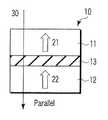
- FIGS. 1A and 1Bare schematic views showing an MTJ element with a single pin structure according to an embodiment of the present invention
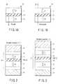
- FIG. 2is a schematic sectional view showing Detailed Example 1-1 of the MTJ element according to an embodiment of the present invention
- FIG. 3is a schematic sectional view showing Detailed Example 1-2 of the MTJ element according to an embodiment of the present invention.
- FIG. 4is a schematic sectional view showing Detailed Example 1-5 of the MTJ element according to an embodiment of the present invention.
- FIGS. 5A and 5Bare schematic sectional views showing another example of Detailed Example 1-5 of the MTJ element according to an embodiment of the present invention.
- FIGS. 6A and 6Bare schematic sectional views showing still another example of Detailed Example 1-5 of the MTJ element according to an embodiment of the present invention.
- FIG. 7is a schematic sectional view showing Detailed Example 1-6 of the MTJ element according to an embodiment of the present invention.
- FIG. 8is a schematic sectional view showing Detailed Example 1-7 of the MTJ element according to an embodiment of the present invention.
- FIGS. 9A and 9Bare schematic views showing an MTJ element with a dual pin structure 1 according to an embodiment of the present invention.
- FIG. 10is a schematic sectional view showing Detailed Example 2-1 of the MTJ element according to an embodiment of the present invention.
- FIGS. 11A and 11Bare schematic views showing an MTJ element with a dual pin structure 2 according to an embodiment of the present invention.
- FIG. 12is a schematic sectional view showing Detailed Example 3 of the MTJ element according to an embodiment of the present invention.
- FIGS. 15A and 15Bare graphs showing the relationship between the damping constant, saturation magnetization, and magnetic anisotropy energy according to an embodiment of the present invention.
- FIGS. 16A to 16 Dare schematic views showing forms in which a material with a small damping constant or a material with a large damping constant is dispersed according to an embodiment of the present invention
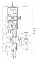
- FIG. 17is a schematic sectional view showing a magnetoresistive random access memory according to the first embodiment of the present invention.
- FIG. 18is a schematic sectional view showing a magnetoresistive random access memory according to the second embodiment of the present invention.
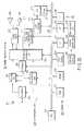
- FIG. 19is a block diagram showing Application Example 1 which applies a magnetoresistive random access memory according to an embodiment of the present invention to a modem;
- FIG. 20is a block diagram showing Application Example 2 which applies a magnetoresistive random access memory according to an embodiment of the present invention to a cellular phone terminal;
- FIG. 21is a plan view showing Application Example 3 which applies a magnetoresistive random access memory according to an embodiment of the present invention to an MRAM card to store media contents;
- FIG. 22is a plan view showing a card insertion type data transfer device to transfer data to the MRAM card in FIG. 21 ;
- FIG. 23is a sectional view showing the card insertion type data transfer device to transfer data to the MRAM card in FIG. 21 ;
- FIG. 24is a sectional view showing a fitting type data transfer device to transfer data to the MRAM card in FIG. 21 ;
- FIG. 25is a sectional view showing a slide type data transfer device to transfer data to the MRAM card in FIG. 21 .
- a magnetic tunnel junction (MTJ) elementis used as a magnetoresistive element.
- FIGS. 1A and 1Bare schematic views showing an MTJ element with a single pin structure according to an embodiment of the present invention.
- the MTJ element with a single pin structure according to an embodiment of the present inventionwill be described below.
- an MTJ element 10has a layered structure including a free layer (recording layer) 11 formed from a magnetic layer, a pinned layer (fixed magnetic layer) 12 formed from a magnetic layer, and a nonmagnetic layer 13 sandwiched between the free layer 11 and the pinned layer 12 .
- the MTJ element 10is of so-called perpendicular magnetization type in which a magnetization direction 21 of the free layer 11 and a magnetization direction 22 of the pinned layer 12 are perpendicular to the film surface.
- the MTJ element 10When the nonmagnetic layer 13 is made of an insulator, the MTJ element 10 has a tunneling magnetoresistive (TMR) effect. When the nonmagnetic layer 13 is made of a metal, the MTJ element 10 has a giant magnetoresistive (GMR) effect.
- the nonmagnetic layer 13 made of an insulatoruses, e.g., MgO (magnesium oxide) or AlO (aluminum oxide; e.g., Al 2 O 3 ).
- the nonmagnetic layer 13 made of a metaluses, e.g., Cu, Pt or Au.
- the magnetizations of the two magnetic layersare arranged parallel ( FIG. 1A ) or antiparallel ( FIG. 1B ).
- the resistance value which changes depending on the magnetization arrangement statecorresponds to “0” or “1” information.
- a spin polarized current 30is supplied to the MTJ element 10 to change the magnetization direction 21 of the free layer 11 and write information. Spin-polarized electrons flow in a reverse direction to the spin polarized current 30 .
- the spin polarized current 30flows from the free layer 11 to the pinned layer 12 , as shown in FIG. 1A , the spin-polarized electrons are injected from the pinned layer 12 to the free layer 11 so that the magnetization direction 22 of the pinned layer 12 and the magnetization direction 21 of the free layer 11 are arranged parallel.
- the spin polarized current 30flows from the pinned layer 12 to the free layer 11 , as shown in FIG. 1B , the spin-polarized electrons flow from the free layer 11 to the pinned layer 12 . Electrons having spin parallel to the pinned layer 12 are transmitted. Electrons having spin antiparallel to the pinned layer 12 are reflected. As a result, the magnetization direction 21 of the free layer 11 and the magnetization direction 22 of the pinned layer 12 are arranged antiparallel.
- a high-performance MTJ element 10can be implemented.
- the reversal currentis proportional to saturation magnetization, anisotropy field, and volume. By appropriately adjusting them, the difference in reversal current between the free layer 11 and the pinned layer 12 can be ensured.
- a material having a high magnetocrystalline anisotropy energy density of, e.g., 5 ⁇ 10 5 erg/cc or moreis preferably used. Detailed examples will be described below.
- Alloys having Co as a principal component and containing at least one element of Cr, Ta, Nb, V, W, Hf, Ti, Zr, Pt, Pd, Fe, and Niare a CoCr alloy, CoPt alloy, CoCrTa alloy, CoCrPt alloy, CoCrPtTa alloy, and CoCrNb alloy. These alloys can adjust the magnetic anisotropy energy density and saturation magnetization by increasing the ratio of the nonmagnetic element.
- Ordered alloys containing at least one element of Fe, Co, and Ni and at least one element of Pt and Pd and having an L1 0 crystal structureare Fe 50 Pt 50 , Fe 50 Pd 50 , Co 50 Pt 50 , Fe 30 Ni 20 Pt 50 , Co 30 Fe 20 Pt 50 , and CO 30 Ni 20 Pt 50 .
- These ordered alloysare not limited to the above composition ratios.
- an impurity elementsuch as Cu (copper), Cr, or Ag (silver), an alloy thereof, or an insulator is added to these ordered alloys, the magnetic anisotropy energy density and saturation magnetization can be adjusted low.
- Ferrimagnetic materialsmade of alloys of rare-earth metals and transition metals. Examples are amorphous alloys made of Tb (terbium), Dy (dysprosium), or Gd (gadolinium), and at least one element of transition metals. Examples are TbFe, TbCo, TbFeCo, DyTbFeCo, and GdTbCo. These alloys can adjust the magnetic anisotropy energy density and saturation magnetization by adjusting the composition.
- the magnetic and nonmagnetic portionsmay be separated by segregating the nonmagnetic portion.
- an oxidesuch as SiO 2 or MgO, a nitride such as SiN, or a carbide such as SiC may be used as the nonmagnetic portion.
- an alloysuch as a nonmagnetic CoCr alloy with a Cr concentration of 25 at % or more may be used.
- a magnetic metal layer made of a highly spin-polarized material, i.e., at least one element of Fe, Co, and Ni or an alloy containing the elementmay be arranged on the interface between the magnetic layer (free layer 11 or pinned layer 12 ) and the nonmagnetic layer 13 of the MTJ element 10 to increase the magnetoresistive (MR) ratio. Since the magnetic layers normally have in-plane magnetization as a monolayer, the magnetic thickness ratio to the stacked perpendicular magnetic anisotropy material must be adjusted not to deteriorate the stability of perpendicular magnetization.
- the free layer 11 and pinned layer 12may have a structure including stacked magnetic layers.
- One of the magnetic layersmay be a so-called granular structure in which a magnetic material is dispersed.
- the MTJ element 10 with a single pin structureto direct the magnetization directions 21 and 22 of the free layer 11 and pinned layer 12 in the direction perpendicular to the film surface, magnetic anisotropy in the perpendicular direction is necessary.
- the magnetic anisotropydepends on the magnetocrystalline anisotropy, it does not depend on the shape. Even when the pattern size of the magnetic film is small, the anisotropy field does not change. Hence, microfabrication can be implemented without increasing the reversal current density only when the magnetic film is formed as a perpendicular magnetic film.
- MRAMmagnetoresistive random access memory
- a free layer 11is made of an artificial lattice
- a pinned layer 12is made of an ordered alloy.
- FIG. 2is a schematic sectional view showing Detailed Example 1-1 of the MTJ element according to an embodiment of the present invention. Detailed Example 1-1 of the MTJ element 10 will be described below.
- the MTJ element 10has a structure in which an underlayer 15 , pinned layer 12 , tunnel barrier layer TB (nonmagnetic layer 13 ), free layer 11 , and cap layer 16 are stacked in an order named.
- the underlayer 15is used to improve the crystalline orientation of MTJ.
- a lower electrode 14is provided on the lower surface of the underlayer 15 .
- An upper electrode 17is provided on the upper surface of the cap layer 16 .
- the pinned layer 12needs to have a magnetization reversal current larger than that of the free layer 11 , and for this, saturation magnetization, anisotropy field, and thickness are adjusted, as described above.
- saturation magnetization, anisotropy field, and thicknessare adjusted, as described above.
- a (001) plane with a face centered tetragonal (fct) structuremust be oriented.
- a very thin underlayerhaving a thickness of several nm and made of MgO (magnesium oxide) is used as the underlayer 15 .
- an element or compounde.g., an alloy having a face centered cubic (fcc) structure or body centered cubic (bcc) structure with a lattice constant of about 2.8 ⁇ , 4 ⁇ , or 5.6 ⁇ , e.g., Pt, Pd, Ag, Au, Al, or Cr or an alloy mainly containing them may be used.
- fccface centered cubic
- bccbody centered cubic
- the magnetization reversal current of the free layer 11must be smaller than that of the pinned layer 12 .
- Saturation magnetization, anisotropy field, and thicknessare adjusted, as described above, to make the current smaller than that of the pinned layer 12 .
- the coercive forcecan be adjusted by adjusting the thickness of the Co and Pt.
- the layered structure of Detailed Example 1-1 of the MTJ element 10will be described below.
- the lower electrode 14is made of a 10-nm thick Ta film.
- the underlayer 15is made of a 3-nm thick Pt film formed on a 0.5-nm thick MgO film.
- the MgO/Pt layered filmhas a (001) plane oriented.
- the pinned layer 12is made of a 10-nm thick Fe 50 Pt 50 film with a (001) plane being oriented.
- the tunnel barrier layer TBis made of a 1.5-nm thick MgO film.
- the free layer 11is made of a layered film of [Co/Pt]5 formed by stacking five periods each including a 0.45-nm thick Co film and a 1.5-nm thick Pt film.
- the cap layer 16is made of a 3-nm thick Pt film.
- the upper electrode 17is made of a layered film having a 10-nm thick Ru film formed on a 10-nm thick Ta
- the coercive force and saturation magnetizationare measured by using a vibrating sample magnetometer.
- the coercive force and saturation magnetizationare 5 kOe and 700 emu/cc in the pinned layer 12 and 130 Oe and 340 emu/cc in the free layer 11 .
- a Pt layermay be inserted in the interface between the tunnel barrier layer TB and Co of the free layer 11 unless the MR ratio decreases largely.
- a Co 50 Pt 50 ordered layer or Co 30 Fe 20 Pt 50 ordered layermay be used in place of the above-described Fe 50 Pt 50 ordered layer.
- the pinned layer 12e.g., (Fe 50 Pt 50 ) 88 —(SiO 2 ) 12 may be used which is a structure formed by dividing the above-described structure by, e.g., SiO 2 or MgO.
- a Co/Pd artificial latticemay be used in place of the Co/Pt artificial lattice.
- Al—Omay be used.
- the stack order of the free layer 11 and pinned layer 12may be reversed.
- the MTJ element 10has the following layered structure.
- the lower electrode 14is made of a 10-nm thick Ta film.
- the underlayer 15is made of a 3-nm thick Pt film formed on a 0.5-nm thick MgO film.
- the free layer 11is made of a [Co/Pt]4/Co artificial lattice formed by stacking five ach including a 0.3-nm thick Co film and a 1.5-nm thick Pt film. By the underlayer 15 , Pt of the artificial lattice is oriented to a (001) plane.
- the tunnel barrier layer TBis made of a 1.5-nm thick MgO film and oriented to a (001) plane reflecting the orientation of the artificial lattice of the free layer 11 .
- the pinned layer 12is made of a 10-nm thick Fe 50 Pt 50 film whose (001) plane is oriented reflecting the MgO (001) plane.
- the cap layer 16is made of a 3-nm thick Pt film.
- the upper electrode 17is made of a layered film having a 10-nm thick Ru film formed on a 10-nm thick Ta film. Even in this stack order, the coercive forces and saturation magnetizations of the free layer 11 and pinned layer 12 exhibit the same values as described above.
- the tunnel barrier layer TBsince Fe 50 Pt 50 is used as the pinned layer 12 , MgO with a (001) plane being oriented is particularly preferable as the tunnel barrier layer TB.
- the artificial lattice [Co/Pt]4/Co as the free layer 11need not always be oriented to the (001) plane. It may be oriented to a (111) plane.
- the (111) plane of Ptcan be oriented by, e.g., forming the underlayer 15 made of a 5-nm thick Pt film on the lower electrode 14 made of a 10-nm thick Ta film.
- an artificial lattice [Co/Pt]4/Co 60 Fe 20 B 20is used by forming a 0.5-nm thick Co 60 Fe 20 B 20 film instead of Co of the [Co/Pt]4/Co artificial lattice as the free layer 11 on the interface side of the tunnel barrier layer TB.
- an antiferromagnetic layermay be provided adjacent.
- an alloy of Mn and Fe, Ni, Pt, Pd, Ru, Os, or Iri.e., FeMn, NiMn, PtMn, PdMn, PtPdMn, RuMn, OsMn, IrMn, or CrPtMn can be used.
- An MTJ element 10 of Detailed Example 1-2is a modification of Detailed Example 1-1.
- a highly spin-polarized layeris formed on each of the interface between a tunnel barrier layer TB and a free layer 11 and the interface between the tunnel barrier layer TB and a pinned layer 12 .
- FIG. 3is a schematic sectional view showing Detailed Example 1-2 of the MTJ element according to an embodiment of the present invention. Detailed Example 1-2 of the MTJ element 10 will be described below.
- a first highly spin-polarized layer 18is provided on the interface between a pinned layer 12 and a tunnel barrier layer TB.
- a second highly spin-polarized layer 19is provided on the interface between a free layer 11 and the tunnel barrier layer TB.
- the first highly spin-polarized layer 18is exchange-coupled to the pinned layer 12 .
- the second highly spin-polarized layer 19is exchange-coupled to the free layer 11 .
- the second highly spin-polarized layer 19is preferably thinner than the first highly spin-polarized layer 18 to reverse the free layer 11 at a lower current density than the pinned layer 12 .
- the magnetic thickness represented by the product of the volume and saturation magnetization Msis preferably made less in the free layer 11 than in the pinned layer 12 .
- the saturation magnetization Msis reduced, the film thickness is reduced, or the magnetic anisotropy energy is reduced.
- Each of the first and second highly spin-polarized layers 18 and 19is formed from a magnetic metal layer containing at least one element of, e.g., Fe, Co, and Ni. At least one of the first and second highly spin-polarized layers 18 and 19 may be made of a ferromagnetic alloy which contains at least one element of Fe, Co, and Ni and at least one element of B, Nb, Zr, Ta, V, and W and has a boo crystal structure.
- a lower electrode 14is made of a 10-nm thick Ta film.
- An underlayer 15is made of a 3-nm thick Pt film formed on a 0.5-nm thick MgO film.
- the MgO/Pt layered filmhas a (001) plane oriented.
- the pinned layer 12is made of a 15-nm thick Co 50 Pt 50 film with a (001) plane being oriented.
- the first highly spin-polarized layer 18is made of a 1.5-nm thick Co 62 Fe 22 B 16 film.
- the tunnel barrier layer TBis made of a 1.5-nm thick MgO film.
- the second highly spin-polarized layer 19is made of a 1.0-nm thick CO 62 Fe 22 B 16 film.
- the free layer 11is made of a layered film of [Pd/Co]4 formed by stacking four periods each including a 0.7-nm thick Pd film and a 0.3-nm thick Co film.
- a cap layer 16is made of a 3-nm thick Pd film.
- An upper electrode 17is made of a layered film having a 10-nm thick Ru film formed on a 10-nm thick Ta film.
- the coercive force and saturation magnetizationare measured by using a vibrating sample magnetometer.
- the coercive force and saturation magnetizationare 3.5 kOe and 750 emu/cc in the pinned layer 12 and 250 Oe and 500 emu/cc in the free layer 11 .
- the pinned layer 12 and first highly spin-polarized layer 18are exchange-coupled and behave as one magnetic layer.
- the free layer 11 and second highly spin-polarized layer 19are exchange-coupled and behave as one magnetic layer.
- the above-described coercive forces and saturation magnetizationsare values obtained when the layers are regarded as single magnetic materials.
- the magnetoresistive ratio of the MTJ element 10is 120%.
- the pinned layer 12e.g., (Co 50 Pt 50 ) 90 —(MgO) 10 may be used which is a structure formed by dividing the above-described structure by, e.g., SiO 2 or MgO.
- a CoCr/Pd artificial latticemay be used in place of the Co/Pd artificial lattice.
- the tunnel barrier layer TBAl—C may be used.
- the stack order of the free layer 11 and pinned layer 12may be reversed.
- an antiferromagnetic layermay be provided adjacent.
- an alloy of Mn and Fe, Ni, Pt, Pd, Ru, Os, or Iri.e., FeMn, NiMn, PtMn, PtPdMn, RuMn, OsMn, IrMn, or CrPtMn can be used.
- An MTJ element 10 of Detailed Example 1-3has the same layered structure as that of Detailed Example 1-2 shown in FIG. 3 .
- a highly spin-polarized layeris provided on each of the interface between a tunnel barrier layer TB and a free layer 11 and the interface between the tunnel barrier layer TB and a pinned layer 12 .
- Each highly spin-polarized layeris made of Co, Fe, a Co—Fe alloy, and an Fe—Ni alloy which are stacked with the (001) plane of a bcc structure oriented.
- An L1 0 ordered alloy with a (001) plane being orientedis also stacked.
- the L1 0 ordered alloymay be either the free layer or the pinned layer.
- a lower electrode 14is made of a 10-nm thick Ta film.
- An underlayer 15is made of a 3-nm thick Pt film formed on a 0.5-nm thick MgO film.
- the MgO/Pt layered filmhas a (001) plane oriented.
- the pinned layer 12is made of a 15-nm thick Fe 50 Pt 50 film with a (001) plane being oriented.
- a first highly spin-polarized layer 18is made of a 1.0-nm thick Fe film. Fe has the (001) plane of a bcc structure oriented.
- the tunnel barrier layer TBis made of a 1.5-nm thick MgO film with a (001) plane being oriented.
- a second highly spin-polarized layer 19is made of a 0.5-nm thick Co 50 Fe 50 film. Co 50 Fe 50 has the (001) plane of a boc structure oriented.
- the free layer 11is made of a layered film of [Co/Pt]4 formed by stacking four periods each including a 0.7-nm thick Pd film and a 0.3-nm thick Co film.
- a cap layer 16is made of a 3-nm thick Pd film.
- An upper electrode 17is made of a layered film having a 10-nm thick Ru film formed on a 10-nm thick Ta film.
- the coercive force and saturation magnetizationare measured by using a vibrating sample magnetometer.
- the coercive force and saturation magnetizationare 4.5 kOe and 800 emu/cc in the pinned layer 12 and 200 Oe and 550 emu/cc in the free layer 11 .
- the pinned layer 12 and first highly spin-polarized layer 18are exchange-coupled and behave as one magnetic layer.
- the free layer 11 and second highly spin-polarized layer 19are exchange-coupled and behave as one magnetic layer.
- the above-described coercive forces and saturation magnetizationsare values obtained when the layers are regarded as single magnetic materials.
- the magnetoresistive ratio of the MTJ element 10is 120%.
- An MTJ element 10 of Detailed Example 1-4has the same layered structure as that of Detailed Example 1-2 shown in FIG. 3 .
- a highly spin-polarized layeris provided on each of the interface between a tunnel barrier layer TB and a free layer 11 and the interface between the tunnel barrier layer TB and a pinned layer 12 .
- At least one of the free layer 11 and pinned layer 12is made of an RE-TM amorphous alloy having a rare-earth metal (RE) and transition metal (TM).
- RErare-earth metal
- TMtransition metal
- a lower electrode 14is made of a 10-nm thick Ta film.
- An underlayer 15is made of a 5-nm thick Ru film.
- the pinned layer 12is made of a 30-nm thick (Co 78 Pt 12 Cr 10 ) 85 —(SiO 2 ) 15 film with a (002) plane being oriented.
- a first highly spin-polarized layer 18is made of a 2.0-nm thick Co 62 Fe 22 B 16 film.
- the tunnel barrier layer TBis made of a 1.0-nm thick MgO film.
- a second highly spin-polarized layer 19is made of a 1.0-nm thick CO 60 Fe 20 B 20 film.
- the free layer 11is made of a 10-nm thick Tb 27 (Fe 71 Co 29 ) 73 film.
- a cap layer 16is made of a 3-nm thick Pt film.
- An upper electrode 17is made of a layered film having a 10-nm thick Ru film formed on a 10-nm thick Ta film.
- the coercive force and saturation magnetizationare measured by using a vibrating sample magnetometer.
- the coercive force and saturation magnetizationare 4.0 kOe and 500 emu/cc in the pinned layer 12 and 500 Oe and 300 emu/cc in the free layer 11 .
- the pinned layer 12 and first highly spin-polarized layer 18are exchange-coupled and behave as one magnetic layer.
- the free layer 11 and second highly spin-polarized layer 19are exchange-coupled and behave as one magnetic layer.
- the above-described coercive forces and saturation magnetizationsare values obtained when the layers are regarded as single magnetic materials.
- the magnetoresistive ratio of the MTJ element 10is 100%.
- the pinned layer 12may be made of a 50-nm thick Tb 22 (Fe 71 Co 29 ) 78 film.
- the RE-TM amorphous alloysuch as Tb 22 (Fe 71 Co 29 ) 78 is an amorphous alloy
- the 5-nm thick Ru film used as the underlayer 15is not always necessary.
- a Pt, Ru, or SiN filmmay be formed as a buffer layer to smoothly form the RE-TM alloy.
- the coercive force and saturation magnetization measured by the vibrating sample magnetometerwere 8 kOe and 200 emu/cc.
- the pinned layer 12 and first highly spin-polarized layer 18are exchange-coupled and behave as one magnetic layer.
- the above-described coercive force and saturation magnetizationare values obtained when the layers are regarded as a single magnetic material.
- a synthetic ferrimagnetic structure(a structure in which a magnetic layer and a metal layer are alternately stacked) may be used as the pinned layer 12 .
- the magnetic layer of the synthetic ferrimagnetic structureare Fe, Co, Ni, and alloys thereof.
- the metal layer of the synthetic ferrimagnetic structureare Ru, Ir, Rh, Re, and Os.
- Detailed examples of the synthetic ferrimagnetic structureare Co/Ru, Co/Ir, and Co/Rh.
- the pinned layer 12is made of an artificial lattice [Ru/Co]15 formed by stacking 15 periods each including a 0.8-nm thick Ru film and a 0.3-nm thick Co film.
- the tunnel barrier layer TBAl—O may be used.
- the stack order of the free layer 11 and pinned layer 12may be reversed.
- an antiferromagnetic layermay be provided adjacent.
- an alloy of Mn and Fe, Ni, Pt, Pd, Ru, Os, or Iri.e., FeMn, NiMn, PtMn, PtPdMn, RuMn, OsMn, IrMn, or CrPtMn can be used.
- An MTJ element of Detailed Example 1-5has a synthetic antiferro (SAF) structure in which two magnetic layers included in a pinned layer 12 are antiferromagnetically exchange-coupled.
- SAFsynthetic antiferro
- FIG. 4is a schematic sectional view showing Detailed Example 1-5 of the MTJ element according to an embodiment of the present invention. Detailed Example 1-5 of an MTJ element 10 will be described below.
- the pinned layer 12includes a first magnetic layer 34 , a second magnetic layer 36 , and a first nonmagnetic layer 35 provided between the first and second magnetic layers 34 and 36 , and has an SAF structure in which the first and second magnetic layers 34 and 36 are antiferromagnetically exchange-coupled.
- magnetizations 22 - 1 and 22 - 2 of the first and second magnetic layers 34 and 36are antiparallel, leakage fields from the first and second magnetic layers 34 and 36 are canceled.
- the leakage field of the pinned layer 12can be reduced.
- the volume of the exchange-coupled magnetic layers 34 and 36increases, the thermal agitation is suppressed.
- a lower electrode 14is made of a 10-nm thick Ta film.
- An underlayer 15is made of a 5-nm thick Ru film.
- the first magnetic layer 34is made of a 20-nm thick (Co 78 Pt 12 Cr 10 ) 85— (SiO 2 ) 15 film with a (002) plane being oriented.
- the first nonmagnetic layer 35is made of a 0.9-nm thick Ru film.
- the second magnetic layer 36is made of a 15-nm thick (Co 78 Pt 12 Cr 10 ) 85 —(SiO 2 ) 15 film.
- a first highly spin-polarized layer 18is made of a 1.0-nm thick Co 62 Fe 22 B 16 film.
- the tunnel barrier layer TBis made of a 1.0-nm thick MgO film.
- a free layer 11is made of a layered film of [Co/Pt]5 formed by stacking five periods each including a 0.4-nm thick Co film and a 0.8-nm thick Pt film.
- the first Co layer of the layered film of [Co/Pt]5 formed on the MgO filmfunctions as a second highly spin-polarized layer 19 .
- a cap layer 16is made of a 3-nm thick Pt film.
- An upper electrode 17is made of a layered film having a 10-nm thick Ru film formed on a 10-nm thick Ta film.
- the first nonmagnetic layer 35 to couple the magnetic layers 34 and 36 antiferromagneticallycan be made of at least one element of Ru, Os, Re, and Rh or an alloy mainly containing them.
- Antiferromagnetic couplingcan also be implemented even when the first and second magnetic layers 34 and 36 are made of a ferrimagnetic material of an RE-TM alloy. In this case, the first nonmagnetic layer 35 need not always be used. An example will be described below with reference to FIGS. 5A and 5B .
- RE-TM alloythe magnetic moment of a rare-earth metal (RE) and that of a transition metal (TM) are antiferromagnetically coupled.
- RE-TM alloysWhen RE-TM alloys are stacked, REs are ferromagnetically coupled while TMs are ferromagnetically coupled, as is known. Since the magnetic moments of the RE and TM cancel each other, the magnetic moment of an RE-TM alloy can be adjusted by the composition.
- a remaining magnetic moment 43is directed in the same direction as the magnetic moment 41 of RE.
- An RE-TM alloy layer 52 in which a magnetic moment 44 of RE is larger than a magnetic moment 45 of TMis formed on the RE-TM alloy layer 51 .
- the magnetic moments 41 and 44 of REsare directed in the same direction while the magnetic moments 42 and 45 of TMs are directed in the same direction.
- the magnetic moments 43 and 46 of the two RE-TM alloy layers 51 and 52are directed in the same direction so that they are arranged parallel.
- a so-called compensation compositioncan be obtained so that the magnetic moment becomes zero because the magnitude of the magnetic moment of Tb equals that of the magnetic moment of Co.
- Tb 25 Co 75 film and a 10-nm thick Tb 20 Co 80 filmare stacked, their magnetic moments are antiparallel.
- the MTJ element 10 in which two magnetic layers included in the pinned layer 12 are antiparallelly coupledcan be formed.
- the pinned layer 12 shown in FIG. 4is formed by stacking the two, first and second magnetic layers 34 and 36 each made of an RE-TM alloy.
- the first magnetic layer 34is made of a 20-nm thick Tb 22 (Fe 71 Co 29 ) 78 film
- the second magnetic layer 36is made of a 15-nm thick Tb 26 (Fe 71 Co 29 ) 74 film.
- the compensation compositionis Tb 24 (Fe 71 Co 29 ) 76 .
- antiferromagnetic couplingcan be implemented by providing the first nonmagnetic layer 35 between the first and second magnetic layers 34 and 36 .
- An examplewill be described below with reference to FIGS. 6A and 6B .
- the magnetic moments 42 and 45 of the first and second magnetic layers 51 and 52 shown in FIG. 6Aare supposed to exchange-couple through a nonmagnetic layer 54 .
- the magnetic moments 42 and 48 of the first and second magnetic layers 51 and 53 shown in FIG. 6Bare supposed to exchange-couple through the nonmagnetic layer 54 .
- the magnetic moment 41 of RE of the RE-TM alloy layer 51is made larger than the magnetic moment 42 of TM
- the magnetic moment 44 of RE of the RE-TM alloy layer 52is made larger than the magnetic moment 45 of TM.
- the nonmagnetic layer 54contributes to antiferromagnetic coupling, the magnetic moments of TM and RE are canceled each other by making the magnitude relationship between the magnetic moment 42 of TM and the magnetic moment 41 of RE equal to that between the magnetic moment 45 of TM and the magnetic moment 44 of RE.
- the magnetic moments 43 and 46 of the first and second magnetic layers 51 and 52are arranged antiparallel.
- the nonmagnetic layer 54 to antiferromagnetically couple Cocan be made of at least one element of Ru, Rh, Os, and Re or an alloy mainly containing them.
- the magnetic moment 41 of RE of the RE-TM alloy layer 51is made larger than the magnetic moment 42 of TM, and the magnetic moment 47 of RE of the RE-TM alloy layer 53 is made smaller than the magnetic moment 48 of TM. If the nonmagnetic layer 54 contributes to ferromagnetic coupling, the magnetic moments of TM and RE are canceled each other by making the magnitude relationship between the magnetic moment 42 of TM and the magnetic moment 41 of RE reverse to that between the magnetic moment 48 of TM and the magnetic moment 47 of RE. Hence, the magnetic moments 43 and 49 of the first and second magnetic layers 51 and 53 are arranged antiparallel.
- the nonmagnetic layer 54 to ferromagnetically couple Cocan be made of at least one element of Pt and Pd or an alloy mainly containing them.
- the first magnetic layer 51 , nonmagnetic layer 54 , and the second magnetic layer 52 or 53 shown in FIGS. 6A and 6Bare made to correspond to the first magnetic layer 34 , nonmagnetic layer 35 , and second magnetic layer 36 of the pinned layer 12 shown in FIG. 4 .
- an antiferromagnetic layermay be provided adjacent.
- an alloy of Mn and Fe, Ni, Pt, Pd, Ru, Os, or Iri.e., FeMn, NiMn, PtMn, PtPdMn, RuMn, OsMn, IrMn, or CrPtMn can be used.
- An RE-TM alloy in which the magnetic moment of RE is larger than that of TM and a metal or alloy mainly containing a transition metalmay be stacked.
- a free layer 11is made of an artificial lattice with an SAF structure.
- FIG. 7is a schematic sectional view showing Detailed Example 1-6 of the MTJ element according to an embodiment of the present invention. Detailed Example 1-6 of an MTJ element 10 will be described below.
- the free layer 11includes a first magnetic layer 31 , first nonmagnetic layer 32 , and second magnetic layer 33 , and has an SAF structure in which the first and second magnetic layers 31 and 33 are antiferromagnetically exchange-coupled.
- magnetizations 21 - 1 and 21 - 2 of the first and second magnetic layers 31 and 33are antiparallel, leakage fields from the first and second magnetic layers 31 and 33 are canceled.
- the leakage field of the free layer 11can be reduced.
- the volume of the exchange-coupled magnetic layers 31 and 33increases, the thermal agitation is suppressed.
- a lower electrode 14is made of a 10-nm thick Ta film.
- An underlayer 15is made of a 3-nm thick Pt film formed on a 0.5-nm thick MgO film.
- the MgO/Pt layered filmhas a (001) plane oriented.
- a pinned layer 12is made of a 20-nm thick Co 50 Pt 50 film with a (001) plane being oriented.
- a first highly spin-polarized layer 18is made of a 1.5-nm thick Co 62 Fe 22 B 16 film.
- a tunnel barrier layer TBis made of a 1.2-nm thick MgO film.
- a second highly spin-polarized layer 19is made of a 0.8-nm thick Co 63 Fe 17 B 10 film.
- the first magnetic layer 31 of the free layer 11is made of an artificial lattice [Pd/Co]4 formed by stacking four periods each including a 0.7-nm thick Pd film and a 0.3-nm thick Co film.
- the first nonmagnetic layer 32 of the free layer 11is made of a 0.9-nm thick Ru film.
- the second magnetic layer 33 of the free layer 11is made of an artificial lattice [Co/Pd]3 formed by stacking three periods each including a 0.3-nm thick Co film and a 0.7-nm thick Pd film.
- a cap layer 16is made of a 3-nm thick Pd film.
- An upper electrode 17is made of a layered film having a 10-nm thick Ru film formed on a 10-nm thick Ta film.
- an antiferromagnetic layermay be provided adjacent.
- an alloy of Mn and Fe, Ni, Pt, Pd, Ru, Os, or Iri.e., FeMn, NiMn, PtMn, PtPdMn, RuMn, OsMn, IrMn, or CrPtMn can be used.
- the first and second magnetic layers 31 and 33need not be formed from an artificial lattice and may be made of an ordered alloy or disordered alloy.
- An RE-TM alloy in which the magnetic moment of RE is larger than that of TM and a metal or alloy mainly containing a transition metalmay be stacked.
- both a free layer 11 and pinned layer 12have an SAF structure.
- FIG. 8is a schematic sectional view showing Detailed Example 1-7 of an MTJ element according to an embodiment of the present invention. Detailed Example 1-7 of an MTJ element 10 will be described below.
- the free layer 11includes a first magnetic layer 31 , first nonmagnetic layer 32 , and second magnetic layer 33 , and has an SAF structure in which the first and second magnetic layers 31 and 33 are antiferromagnetically exchange-coupled.
- the pinned layer 12includes a first magnetic layer 34 , first nonmagnetic layer 35 , and second magnetic layer 36 , and has an SAF structure in which the first and second magnetic layers 34 and 36 are antiferromagnetically exchange-coupled. In this case, since magnetizations 21 - 1 and 21 - 2 of the first and second magnetic layers 31 and 33 are antiparallel, leakage fields from the first and second magnetic layers 31 and 34 are canceled.
- the leakage field of the free layer 11can be reduced.
- magnetizations 22 - 1 and 22 - 2 of the first and second magnetic layers 34 and 36are antiparallel, leakage fields from the first and second magnetic layers 34 and 36 are canceled.
- the leakage field of the pinned layer 12can be reduced.
- the volume of the magnetic layers 31 and 33 and magnetic layers 34 and 36 which are exchange-coupledincreases, the thermal agitation is suppressed.
- a lower electrode 14is made of a 10-nm thick Ta film.
- An underlayer 15is made of a 5-nm thick Ru film.
- the first magnetic layer 34is made of a 20-nm thick (Co 78 Pt 12 Cr 10 ) 85 —(SiO 2 ) 15 film with a (002) plane being oriented.
- the first nonmagnetic layer 35is made of a 0.9-nm thick Ru film.
- the second magnetic layer 36is made of a 15-nm thick (Co 78 Pt 12 Cr 10 ) 85 —(SiO 2 ) 15 film.
- a first highly spin-polarized layer 18is made of a 1.0-nm thick Co 62 Fe 22 B 16 film.
- a tunnel barrier layer TBis made of a 1.2-nm thick Mgo film.
- a second highly spin-polarized layeris made of a 0.8-nm thick Co 63 Fe 17 B 10 film.
- the first magnetic layer 31 of the free layer 11is made of an artificial lattice [Pd/Co]4 formed by stacking four periods each including a 0.7-nm thick Pd film and a 0.3-nm thick Co film.
- the first nonmagnetic layer 32 of the free layer 11is made of a 0.9-nm thick Ru film.
- the second magnetic layer 33 of the free layer 11is made of an artificial lattice [Co/Pd]3 formed by stacking three periods each including a 0.3-nm thick Co film and a 0.7-nm thick Pd film.
- a cap layer 16is made of a 3-nm thick Pd film.
- An upper electrode 17is made of a layered film having a 10-nm thick Ru film formed on a 10-nm thick Ta film.
- an antiferromagnetic layermay be provided adjacent.
- an alloy of Mn and Fe, Ni, Pt, Pd, Ru, Os, or Iri.e., FeMn, NiMn, PtMn, PtPdMn, RuMn, OsMn, IrMn, or CrPtMn can be used.
- the antiparallel coupling structuremay be obtained by using a layered film of an RE-TM alloy in which the magnitude relationship between the magnetic moment of RE and the magnetic moment of RE is reversed, stacking an RE-TM alloy in which the magnetic moment of RE is larger than that of TM and a metal or alloy mainly containing a transition metal, or forming a so-called SAF structure with a nonmagnetic, e.g., Ru layer sandwiched.
- a nonmagnetice.g., Ru layer sandwiched.
- FIGS. 9A and 9Bare schematic sectional views showing an MTJ element with a dual pin structure 1 according to an embodiment of the present invention.
- the MTJ element with a dual pin structure 1 according to an embodiment of the present inventionwill be described below.
- an MTJ element 10has a layered structure including a free layer 11 formed from a magnetic layer, first and second pinned layers 12 a and 12 b each formed from a magnetic layer, a first nonmagnetic layer 13 a sandwiched between the free layer 11 and the first pinned layer 12 a , and a second nonmagnetic layer 13 b sandwiched between the free layer 11 and the second pinned layer 12 b.
- the MTJ element 10is of so-called perpendicular magnetization type in which a magnetization direction 21 of the free layer 11 and magnetization directions 22 a and 22 b of the pinned layers 12 a and 12 b are perpendicular to the film surface.
- the first and second pinned layers 12 a and 12 bhave an antiparallel magnetization arrangement with the magnetization directions 22 a and 22 b being directed in different directions.
- the MTJ element 10When the first and second nonmagnetic layers 13 a and 13 b are made of an insulator, the MTJ element 10 has a TMR effect. When the first and second nonmagnetic layers 13 a and 13 b are made of a metal, the MTJ element 10 has a GMR effect.
- the first and second nonmagnetic layers 13 a and 13 bmade of an insulator use, e.g., MgO (magnesium oxide) or AlO (aluminum oxide; e.g., Al 2 O 3 ).
- the first and second nonmagnetic layers 13 a and 13 bmade of a metal use, e.g., Cu, Pt or Au.
- the magnetic layers (free layer 11 and pinned layer 12 a ) sandwiching the first nonmagnetic layer 13 a or the magnetic layers (free layer 11 and pinned layer 12 b ) sandwiching the second nonmagnetic layer 13 bhave a parallel or antiparallel magnetization arrangement.
- the parallel arrangement and antiparallel arrangementsimultaneously exist in FIGS. 9A and 9B so the entire magnetoresistance does not change.
- the change in magnetoresistance generated in the tunnel barrier layer TBis larger than that generated in the metal layer.
- the magnetization arrangement through the first nonmagnetic layer 13 acorresponds to “0” or “1” information.
- a parallel arrangementis obtained in FIG. 9A
- an antiparallel arrangementis obtained in FIG. 9B .
- the second nonmagnetic layer 13 bmay be the tunnel barrier layer TB
- the first nonmagnetic layer 13 amay be a metal layer.
- the magnetizations of the two magnetic layersare arranged parallel ( FIG. 9A ) or antiparallel ( FIG. 9B ).
- the resistance value which changes depending on the magnetization arrangement statecorresponds to “0” or “1” information.
- a spin polarized current 30is supplied to the MTJ element 10 to change the magnetization direction 21 of the free layer 11 and write information. Spin-polarized electrons flow in a reverse direction to the spin polarized current 30 .
- the spin polarized current 30flows from the second pinned layer 12 b to the first pinned layer 12 a , as shown in FIG. 9A , the spin-polarized electrons flows from the first pinned layer 12 a to the second pinned layer 12 b.
- upward spinis mainly injected from the first pinned layer 12 a.
- the second pinned layer 12 breadily transmits downward spin in the process of flowing the spin-polarized electrons from the free layer 11 to the second pinned layer 12 b .
- the reflected upward spin-polarized electronsare injected to the free layer 11 so that the magnetization direction 21 of the free layer 11 becomes parallel to the magnetization direction 22 a of the first pinned layer 12 a.
- the magnetization direction 21 of the free layer 11becomes parallel to the magnetization direction 22 b of the second pinned layer 12 b on the basis of the same principle as described above.
- the same materials as in the above-described single pin structurecan be used.
- the same effect as in the single pin structurecan be obtained.
- the effect of reflection of spin-polarized electronscan be used more effectively by providing the pinned layers 12 a and 12 b with the dual pin structure on both sides of the free layer 11 , the reversal current can further be reduced as compared to the single pin structure.
- one pinned layer 12 a of pinned layers 12 a and 12 b provided on both sides of a free layer 11has an SAF structure.
- FIG. 10is a schematic sectional view showing Detailed Example 2-1 of the MTJ element according to an embodiment of the present invention. Detailed Example 2-1 of an MTJ element 10 will be described below.
- the MTJ element 10has a structure in which an underlayer 15 , first pinned layer 12 a , first nonmagnetic layer 13 a , free layer 11 , first highly spin-polarized layer 18 , second nonmagnetic layer 13 b , second highly spin-polarized layer 19 , second pinned layer 12 b , and cap layer 16 are stacked in an order named.
- the first pinned layer 12 ahas an SAF structure including a first magnetic layer 34 , nonmagnetic layer 35 , and second magnetic layer 36 .
- a lower electrode 14is provided on the lower surface of the underlayer 15 .
- An upper electrode 17is provided on the upper surface of the cap layer 16 .
- the layered structure of Detailed Example 2-1 of the MTJ element 10will be described below.
- the lower electrode 14is made of a 10-nm thick Ta film.
- the underlayer 15is made of a 5-nm thick Ru film.
- the first magnetic layer 34is made of a 20-nm thick (Co 78 Pt 12 Cr 10 ) 85 —(SiO 2 ) 15 film with a (002) plane being oriented.
- the nonmagnetic layer 35is made of a 0.9-nm thick Ru film.
- the second magnetic layer 36is made of a 15-nm thick (Co 78 Pt 12 Cr 10 ) 85 —(SiO 2 ) 15 film.
- the first nonmagnetic layer 13 ais made of a 5-nm thick Cu film.
- the free layer 11is made of an artificial lattice [Co/Pt]4 formed by stacking four periods each including a 0.3-nm thick Co film and a 0.7-nm thick Pt film.
- the first highly spin-polarized layer 18is made of a 0.5-nm thick Co 62 Fe 22 B 16 film.
- the tunnel barrier layer TBis made of a 1.5-nm thick MgO film.
- the MgO filmhas a (001) plane oriented.
- the second highly spin-polarized layer 19is made of a 1-nm thick Fe film.
- the Fe filmhas a (001) plane oriented.
- the pinned layer 12 bis made of a 15-nm thick Fe 5 OPtSO film with a (001) plane being oriented.
- the cap layer 16is made of a 3-nm thick Pt film.
- the upper electrode 17is made of a layered film having a 10-nm thick Ru film formed on a 10-nm thick Ta film. The MR ratio generated through the tunnel barrier layer TB is higher than that generated through the nonmagnetic layer 13 a.
- the change in magnetoresistance through MgO as the tunnel barrier layer TBis larger than that through Cu as the first nonmagnetic layer 13 a.
- Informationis stored in accordance with the magnetization arrangement of the magnetic layer that integrates the free layer 11 and first highly spin-polarized layer 18 and the magnetic layer that integrates the second highly spin-polarized layer 19 and second pinned layer 12 b. Since the pinned layer 12 a has the SAF structure with a thickness difference between the magnetic layers, the balance magnetic moment of the pinned layer 12 a and the magnetic moment of the pinned layer 12 b can be set in reverse directions. Hence, the leakage fields from the pinned layers 12 a and 12 b to the free layer 11 can cancel each other.
- the pinned layer 12 acan also be formed by using an RE-TM alloy.
- an RE-TM alloy in which the magnetic moment of RE is larger than that of TMis used, and, e.g., a Co or CoFe alloy mainly containing TM is stacked, as described in Detailed Example 1-5, the magnetic moment of Co or CoFe on the interface of the second nonmagnetic layer 13 a can be set parallel to the magnetic moment of TM of the RE-TM alloy.
- the magnetic moment of Co or CoFecan be set antiparallel to the magnetic moment of the RE-TM alloy (magnetic moment of RE).
- both pinned layers 12 a and 12 b provided on both sides of a free layer 11have a monolayer structure. That is, in Detailed Example 2-2, the pinned layer 12 a shown in FIG. 10 has a monolayer structure.
- Detailed Example 2-2 of an MTJ element 10will be described below with reference to FIG. 10 .
- the MTJ element 10has a structure in which an underlayer 15 , first pinned layer 12 a , first nonmagnetic layer 13 a , free layer 11 , first highly spin-polarized layer 18 , second nonmagnetic layer 13 b , second highly spin-polarized layer 19 , second pinned layer 12 b , and cap layer 16 are stacked in an order named.
- a lower electrode 14is provided on the lower surface of the underlayer 15 .
- An upper electrode 17is provided on the upper surface of the cap layer 16 .
- the layered structure of Detailed Example 2-2 of the MTJ element 10will be described below.
- the lower electrode 14is made of a 10-nm thick Ta film.
- the underlayer 15is made of a layered film obtained by forming a 0.5-nm thick Co 40 Fe 40 B 20 film, a 0.5-nm thick MgO film, and a 2-nm thick Pt film in an order named.
- the pinned layer 12 ais made of a 10-nm thick Fe 50 Pt 50 film with a (001) plane being oriented.
- the first nonmagnetic layer 13 ais made of a 5-nm thick Au film with a (001) plane being oriented.
- the free layer 11is made of a 2-nm thick Fe 38 Cu 12 Pt 50 film with a (001) plane being oriented.
- the first highly spin-polarized layer 18is made of a 0.5-nm thick Fe film.
- the tunnel barrier layer TBis made of a 1.2-nm thick MgO film.
- the MgO filmhas a (001) plane oriented.
- the second highly spin-polarized layer 19is made of a 1-nm thick Fe film.
- the Fe filmhas a (001) plane oriented.
- the pinned layer 12 bis made of a 5-nm thick Fe 50 Pt 50 film with a (001) plane being oriented.
- the cap layer 16is made of a 3-nm thick Pt film.
- the upper electrode 17is made of a layered film having a 10-nm thick Ru film formed on a 10-nm thick Ta film.
- the MR ratio generated through the tunnel barrier layer TBis higher than that generated through the nonmagnetic layer 13 a.
- the coercive force of the pinned layer 12 ais larger than that of the pinned layer 12 b.
- the magnetization arrangement of the pinned layer 12 a and that of the pinned layer 12 bcan be set antiparallel by using the difference in coercive force. That is, magnetization is done twice.
- the magnetization of the pinned layer 12 athat of the free layer 11 and first highly spin-polarized layer 18 which behave as an integrated free layer, and that of the second highly spin-polarized layer 19 and pinned layer 12 b which behave as an integrated pinned layer are arranged in the same direction.
- Magnetic field application of the second timeis done in a reverse direction to the first time.
- the applied magnetic field of the second timeis larger than the coercive force of the second highly spin-polarized layer 19 and pinned layer 12 b which behave as an integrated pinned layer and smaller than that of the pinned layer 12 a.
- the magnetization of the free layer 11 and first highly spin-polarized layer 18 which behave as an integrated free layer and that of the second highly spin-polarized layer 19 and pinned layer 12 b which behave as an integrated pinned layerare arranged in a reverse direction to the magnetization direction of the pinned layer 12 a .
- the magnetization arrangement shown in FIG. 9can be realized.
- the change in magnetoresistance through MgO serving as the tunnel barrier layer TBis larger than that through Au serving as the first nonmagnetic layer 13 a.
- Informationis stored by the magnetization arrangement of the magnetic layer including the free layer 11 and first highly spin-polarized layer 18 and the magnetic layer including the second highly spin-polarized layer 19 and pinned layer 12 b.
- the magnetoresistance through a metal film such as an Au filmis low. Even when a highly spin-polarized layer is provided, the change in magnetoresistance is smaller than in the tunnel barrier layer. Hence, a highly spin-polarized layer can be provided.
- the pinned layer 12 ais made of a 30-nm thick Tb 22 (Fe 71 Co 29 ) 78 layer
- the pinned layer 12 bis made of a 30-nm thick Tb 26 (Fe 71 Co 29 ) 74 layer
- the free layer 11is made of a 5-nm thick Tb 22 (Fe 71 Co 29 ) 78 layer.
- Tb 24 (Fe 71 Co 29 ) 76has a compensation composition.
- the magnetic moment of TMis larger than that of RE.
- the magnetic moment of REis larger than that of TM.
- the same magnetization arrangement as that of the pinned layers 12 a and 12 b in FIG. 9can be realized by only one magnetization in one direction. More specifically, the magnetic moment of TM of the pinned layer 12 b is directed in a reverse direction to the magnetic moment of RE. The magnetization of the entire pinned layer 12 b is directed in a reverse direction to the magnetization direction (direction of the magnetic moment of TM). In addition, Fe serving as the second highly spin-polarized layer 19 is exchange-coupled to the magnetic moment of TM and therefore directed in a reverse direction to the magnetization direction.
- each magnetic layercan appropriately be selected from ordered alloys, disordered alloys, artificial lattices, and RE-TM alloys, as described in Detailed Examples 1-1 to 1-7.
- the pinned layer 12 bmay have an SAF structure.
- the pinned layer 12 amay have a monolayer structure.
- the highly spin-polarized layers 18 and 19are inserted between the tunnel barrier layer TB and the free layer 11 and between the tunnel barrier layer TB and the pinned layer 12 b , respectively.
- the highly spin-polarized layeris provided neither between the nonmagnetic layer 13 a and the free layer 11 nor between the nonmagnetic layer 13 a and the pinned layer 12 a.
- highly spin-polarized layersmay be provided between the nonmagnetic layer 13 a and the free layer 11 and between the nonmagnetic layer 13 a and the pinned layer 12 a . Even in this case, the MR ratio generated through the tunnel barrier layer TB must be higher than that generated through the nonmagnetic layer 13 a.
- the nonmagnetic layers 13 a and 13 bmay be made of an insulator or tunnel barrier exhibiting a tunneling magnetoresistive effect. In this case, when a highly spin-polarized layer is provided on the interface of only one tunnel barrier, the difference between the MR ratios can be ensured.
- an antiferromagnetic layermay be provided adjacent.
- an alloy of Mn and Fe, Ni, Pt, Pd, Ru, Os, or Iri.e., FeMn, NiMn, PtMn, PtPdMn, RuMn, OsMn, IrMn, or CrPtMn can be used.
- FIGS. 11A and 11Bare schematic sectional views showing an MTJ element with a dual pin structure 2 according to an embodiment of the present invention.
- the MTJ element with a dual pin structure 2 according to an embodiment of the present inventionwill be described below.
- an MTJ element 10has a layered structure including a free layer 11 formed from a magnetic layer, first and second pinned layers 12 a and 12 b each formed from a magnetic layer, first nonmagnetic layer 13 a sandwiched between the free layer 11 and the first pinned layer 12 a , and a second nonmagnetic layer 13 b sandwiched between the free layer 11 and the second pinned layer 12 b.
- the free layer 11has an SAF structure including a first magnetic layer 31 , nonmagnetic layer 32 , and second magnetic layer 33 .
- the MTJ element 10is of so-called perpendicular magnetization type in which magnetizations 21 - 1 and 21 - 2 of the free layer 11 and magnetization directions 22 a and 22 b of the pinned layers 12 a and 12 b are perpendicular to the film surface.
- the free layer 11preferably has an SAF structure.
- an RE-TM alloy layer 51 in which a magnetic moment 41 of RE is larger than a magnetic moment 42 of TM and an RE-TM alloy layer 53 in which a magnetic moment 47 of RE is smaller than a magnetic moment 48 of TMmay be stacked to make the magnetic moments of the two RE-TM alloy layers antiparallel.
- the MTJ element 10When the first and second nonmagnetic layers 13 a and 13 b are made of an insulator, the MTJ element 10 has a TMR effect. When the first and second nonmagnetic layers 13 a and 13 b are made of a metal, the MTJ element 10 has a GMR effect.
- the first and second nonmagnetic layers 13 a and 13 bmade of an insulator use, e.g., MgO (magnesium oxide) or AlO (aluminum oxide; e.g., Al 2 O 3 ).
- the first and second nonmagnetic layers 13 a and 13 bmade of a metal use, e.g., Cu, Pt or Au.
- the magnetic layers (the magnetic layer 31 of the free layer 11 and the pinned layer 12 a ) sandwiching the first nonmagnetic layer 13 a or the magnetic layers (the magnetic layer 33 of the free layer 11 and the pinned layer 12 b ) sandwiching the second nonmagnetic layer 13 bhave a parallel or antiparallel magnetization arrangement.
- the parallel arrangement and antiparallel arrangementsimultaneously exist in FIGS. 11A and 11B so the entire magnetoresistance does not change.
- the change in magnetoresistance generated in the tunnel barrier layer TBis larger than that in the metal layer.
- the magnetization arrangement through the first nonmagnetic layer 13 acorresponds to “0” or “1” information.
- a parallel arrangementis obtained in FIG. 11A
- an antiparallel arrangementis obtained in FIG. 11B .
- the second nonmagnetic layer 13 bmay be the tunnel barrier layer TB
- the first nonmagnetic layer 13 amay be a metal layer.
- the nonmagnetic layers 13 a and 13 bmay be made of an insulator or tunnel barrier exhibiting a tunneling magnetoresistive effect. In this case, when a highly spin-polarized layer is provided on the interface of only one tunnel barrier, the difference between the MR ratios can be ensured.
- the magnetizations of the two magnetic layersare arranged parallel ( FIG. 11 ) or antiparallel ( FIG. 11B ).
- the resistance value which changes depending on the magnetization arrangement statecorresponds to “0” or “1” information.
- a spin polarized current 30is supplied to the MTJ element 10 to change the magnetization direction 21 of the free layer 11 and write information. Spin-polarized electrons flow in a reverse direction to the spin polarized current 30 .
- the spin polarized current 30flows from the second pinned layer 12 b to the first pinned layer 12 a , as shown in FIG. 11A , the spin-polarized electrons flows from the first pinned layer 12 a to the second pinned layer 12 b.
- upward spinis mainly injected from the first pinned layer 12 a.
- the second pinned layer 12 breadily transmits upward spin in the process of flowing the electrons from the second magnetic layer 33 of the free layer 11 to the second pinned layer 12 b.
- the reflected downward spin-polarized electronsare injected to the second magnetic layer 33 of the free layer 11 so that the magnetization direction 21 - 1 of the first magnetic layer 31 of the free layer 11 becomes parallel to the magnetization direction 22 a of the pinned layer 12 a , and the magnetization direction 21 - 2 of the second magnetic layer 33 becomes antiparallel to the magnetization direction 22 b of the pinned layer 12 b.
- the currentflows from the second pinned layer 12 b to the first pinned layer 12 a , as shown in FIG.
- the magnetization direction 21 - 1 of the first magnetic layer 31 of the free layer 11becomes antiparallel to the magnetization direction 22 a of the pinned layer 12 a
- the magnetization direction 21 - 2 of the second magnetic layer 33becomes parallel to the magnetization direction 22 b of the pinned layer 12 b.
- the same materials as in the above-described single pin structurecan be used.
- the same effect as in the single pin structurecan be obtained.
- the effect of reflection of spin-polarized electronscan be used more effectively by providing the pinned layers 12 a and 12 b a with the dual pin structure on both sides of the free layer 11 , the reversal current can further be reduced as compared to the single pin structure.
- the free layer 11has an SAF structure, and the magnetization directions of first and second pinned layers 12 a and 12 b are parallel.
- FIG. 12is a schematic sectional view showing Detailed Example 3 of the MTJ element according to an embodiment of the present invention. Detailed Example 3 of an MTJ element 10 will be described below.
- the MTJ element 10has a structure in which an underlayer 15 , first pinned layer 12 a , first highly spin-polarized layer 18 , tunnel barrier layer TB, second highly spin-polarized layer 19 , free layer 11 , second nonmagnetic layer 13 b , second pinned layer 12 b , and cap layer 16 are stacked in an order named.
- the free layer 11has an SAF structure including a first magnetic layer 31 , nonmagnetic layer 32 , and second magnetic layer 33 .
- a lower electrode 14is provided on the lower surface of the underlayer 15 .
- An upper electrode 17is provided on the upper surface of the cap layer 16 .
- the layered structure of Detailed Example 3 of the MTJ element 10will be described below.
- the lower electrode 14is made of a 10-nm thick Ta film.
- the underlayer 15is made of a 3-nm thick Pt film formed on a 0.5-nm thick MgO film.
- the MgO/Pt layered filmhas a (001) plane oriented.
- the first pinned layer 12 ais made of a 20-nm thick Fe 50 Pt 50 film with a (001) plane being oriented.
- the first highly spin-polarized layer 18is made of a 1.5-nm thick Co 62 Fe 22 B 16 film.
- the tunnel barrier layer TBis made of a 1.5-nm thick MgO film.
- the second highly spin-polarized layer 19is made of a 0.5-nm thick Co 63 Fe 17 B 10 film.
- the first magnetic layer 31 of the free layer 11is made of an artificial lattice [Pd/Co]4 formed by stacking four periods each including a 0.7-nm thick Pd film and a 0.3-nm thick Co film.
- the nonmagnetic layer 32 of the free layer 11is made of a 0.9-nm thick Ru film.
- the second magnetic layer 33 of the free layer 11is made of an artificial lattice [Co/Pd]2/Co formed by stacking two periods each including a 0.3-nm thick Co film and a 0.7-nm thick Pd film.
- the second nonmagnetic layer 13 bis made of a 0.8-nm thick MgO film.
- the second pinned layer 12 bis made of layered film inducing a 1.5-nm thick Co 90 Fe 10 film and a 30-nm thick Tb 20 (Fe 80 Co 20 ) 80 film.
- Tb 20 (Fe 80 Co 20 ) 80the magnetic moment of RE is smaller than that of TM so that the magnetization directions 22 a and 22 b of the first and second pinned layers 12 a and 12 b become parallel.
- the cap layer 16is made of a 3-nm thick Pt film.
- the upper electrode 17is made of a layered film having a 10-nm thick Ru film formed on a 10-nm thick Ta film.
- the MR ratio generated through the tunnel barrier layer TB having highly spin-polarized layers inserted to both interfacesis higher than that generated through the nonmagnetic layer 13 b without any highly spin-polarized layer inserted.
- each magnetic layercan appropriately be selected from ordered alloys, disordered alloys, artificial lattices, and RE-TM alloys, as described in Detailed Examples 1-1 to 1-7.
- the highly spin-polarized layers 18 and 19are inserted between the tunnel barrier layer TB and the magnetic layer 31 of the free layer 11 and between the tunnel barrier layer TB and the pinned layer 12 a , respectively.
- the highly spin-polarized layeris provided neither between the nonmagnetic layer 13 b and the magnetic layer 33 of the free layer 11 nor between the nonmagnetic layer 13 b and the pinned layer 12 b.
- highly spin-polarized layersmay be provided between the nonmagnetic layer 13 b and the magnetic layer 33 of the free layer 11 and between the nonmagnetic layer 13 b and the pinned layer 12 b. Even in this case, the MR ratio generated through the tunnel barrier layer TB must be higher than that generated through the nonmagnetic layer 13 b.
- an antiferromagnetic layermay be provided adjacent.
- an alloy of Mn and Fe, Ni, Pt, Pd, Ru, Os, or Iri.e., FeMn, NiMn, PtMn, PtPdMn, RuMn, OsMn, IrMn, or CrPtMn can be used.
- Equation (1)represents a reversal current when the magnetization state reverses from parallel (P) to antiparallel (AP).
- the reversal currentis larger when the magnetization state changes from parallel (P) to antiparallel (AP) than when the magnetization state changes from antiparallel (AP) to parallel (P). The former case will be examined.
- I c ⁇ ⁇ 0 P ⁇ APg ′ ⁇ e ⁇ M s ⁇ V ⁇ ⁇ damp ⁇ ⁇ g ⁇ ( 0 ) ⁇ ( H ext + H ani + 2 ⁇ ⁇ ⁇ ⁇ M s ) ( 1 )
- eis the elementary charge
- Msis the saturation magnetization of the reversed magnetic layer (free layer 11 )
- Vis the volume
- ⁇ dampis the Gilbert's damping constant
- his a constant obtained by dividing the Planck's constant by 2 ⁇
- g′is a g-factor
- g(0)is the function of polarization or the spin transfer efficiency when two magnetic materials make an angle ⁇ .
- equation (2)the first term in the parentheses represents a magnetic anisotropy energy density Ku, and the second term in the parentheses represents the demagnetizing field energy.
- a perpendicular magnetic filmis suitable for microfabrication when the magnetic anisotropy energy density Ku, e.g., magnetocrystalline anisotropy energy density caused by the materials is high, no shape magnetic anisotropy energy density is used, and the aspect ratio of the element shape is about 1. For this reason, the shape anisotropy may be sufficiently smaller than the magnetic anisotropy field caused by the materials.
- Kumagnetic anisotropy energy density caused by the materials
- J c0 P ⁇ APA ⁇ t ⁇ ( K u +2 ⁇ M s 2 ) ⁇ J w (5) must be satisfied.
- the magnetic anisotropy energy density Kumust satisfy 2 ⁇ ⁇ M s 2 ⁇ K u ⁇ 1 2 ⁇ ( J w A ⁇ t - 2 ⁇ ⁇ ⁇ ⁇ M s 2 ) ( 7 )
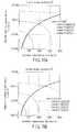
- FIGS. 13A and 13B and FIGS. 14A and 14Bshow relationship (7) in detail.
- FIGS. 13A and 13B and FIGS. 14A and 14Bshow the relationship between the magnetic anisotropy energy density Ku, saturation magnetization Ms, and thickness t of the free layer according to an embodiment of the present invention.
- FIG. 13A and FIG. 14Ashow a case wherein the write current density Jw is 5 MA/cm 2 .
- FIG. 13B and FIG. 14Bshow a case wherein the write current density Jw is 2 MA/cm 2 .
- Examinationsare done for the free layer 11 with the thickness t of 0.5 nm, 1 nm, 3 nm, 5 nm, or 10 nm.
- the magnetic anisotropy energy density Ku, saturation magnetization Ms, and thickness t of the free layer 11must be set in the hatched regions shown in FIGS. 13A and 13B and FIGS. 14A and 14B .
- g( ⁇ ) and the polarization P of a giant magnetoresistive (GMR) with a nonmagnetic layer made of a conductive material such as Cu or Au and a tunneling magnetoresistive (TMR) with a nonmagnetic layer serving as a tunnel barriercan be given by the g-factor g′ is 2.
- g ( ⁇ )P/ ⁇ 2 ⁇ (1+ P 2 ⁇ cos ⁇ ) ⁇ (8)
- g ( ⁇ )⁇ ( P ⁇ 0.5 +P 0.5 ) 3 ⁇ (3+cos ⁇ )/4 ⁇ ⁇ 1 (9)
- the damping constant ⁇ dampwas set to 0.01, and g(0) was set to 0.18.
- the upper limit of the magnetic anisotropy energy density Kuis defined by inequality (7).
- the first termis Jw/(2A ⁇ t).
- the damping constant ⁇ dampwas set to 0.002.
- the efficiency g(0)also changes the ranges of magnetic anisotropy energy density Ku and saturation magnetization Ms.
- the damping constant ⁇ damp, thickness t , and the efficiency g(0)are important, as described above. According to equation (3), Jc is proportional to ⁇ damp ⁇ t/g(0).
- the damping constant ⁇ damp of a magnetic materialis about 0.001 to 0.5.
- the efficiency g(0)can be estimated from the polarization P, as indicated by equations (8) and (9).
- the polarization Pis preferably 0.1 or more.
- the efficiency g(0)is about 0.026 and 0.05 for GMR and TMR, respectively. When the polarization P is 1, the efficiency g(0) is 0.25 for both GMR and TMR.
- the thickness t of the free layer 11will be examined next.
- the upper limit of the magnetic anisotropy energy density Kudecreases as the thickness t increases, as is apparent from inequality (7).
- the magnetic anisotropy energy density Kumust be set small.
- the saturation magnetization Msalso needs to be small. This can also be understood from FIGS. 13A and 13B , and 14 A and 14 B, and it is difficult to make the thickness of the free layer 11 larger than 5 nm.
- the thickness of the free layer 11is preferably set to 5 nm or less.
- the thicknessis also preferably 0.5 nm or more from the viewpoint of in-plane uniformity.
- the thickness t of the free layer 11preferably satisfies a relationship given by 0.5 nm ⁇ t ⁇ 5 nm (10)
- the lower limit value of the thickness of the free layer 11can be supposed to be 0.2 nm or more.
- the thicknesscorresponds to the thickness of each exchange-coupled layer.
- the magnetic anisotropy energy density Kuwill be described next in consideration of the thickness t of the free layer 11 , which is represented by inequality (10). To form a perpendicular magnetic film, the magnetic anisotropy energy density Ku must satisfy Ku>2 ⁇ Ms 2 , as indicated by inequality (6).
- Magnetic materials capable of minimizing the saturation magnetization Msare ferrimagnetic materials and antiferromagnetic materials, and they includes the above-described RE-TM alloy.
- the magnetic anisotropy energy density Ku of the RE-TM alloyis 1 ⁇ 10 5 erg/cc or more. This can be regarded as the lower limit value of the magnetic anisotropy energy density Ku.
- the upper limit value of the magnetic anisotropy energy density Kucan be derived from the relationship shown in FIGS. 15A and 15B . More specifically, as shown in FIG. 15A , when the write current density Jw is 5 MA/cm 2 , 4.1 ⁇ 10 7 erg/cc, i.e., the maximum value in the hatched region is the upper limit value of the magnetic anisotropy energy density Ku. As shown in FIG. 15B , when the write current density Jw is 2 MA/cm 2 , 1.6 ⁇ 10 7 erg/cc, i.e., the maximum value in the hatched region is the upper limit value of the magnetic anisotropy energy density Ku.
- the magnetic anisotropy energy density Kupreferably satisfies 1 ⁇ 10 5 erg/cc ⁇ Ku ⁇ 4.1 ⁇ 10 7 erg/cc (11)
- the magnetic anisotropy energy density Kupreferably satisfies 1 ⁇ 10 5 erg/cc ⁇ Ku ⁇ 1.6 ⁇ 10 7 erg/cc (12)
- the saturation magnetization Mswill be described next in consideration of the thickness t of the free layer 11 , which is represented by inequality (10).
- the saturation magnetization Mscan be derived from the relationship shown in FIGS. 15A and 15B . More specifically, as shown in FIG. 15A , when the write current density Jw is 5 MA/cm 2 , the saturation magnetization Ms is preferably 0 to 2090 emu/cc. As shown in FIG. 15B , when the write current density Jw is 2 MA/cm 2 , the saturation magnetization Ms is preferably 0 to 1320 emu/cc.
- the saturation magnetization Mswhen the write current density Jw is 5 MA/cm 2 or less, the saturation magnetization Ms preferably satisfies 0 ⁇ Ms ⁇ 2090 emu/cc (13) When the write current density Jw is 2 MA/cm 2 or less, the saturation magnetization Ms preferably satisfies 0 ⁇ Ms ⁇ 1320 emu/cc (14)
- the write current density Jwis preferably 5 MA/cm 2 or less.
- the magnetic anisotropy energy density Kupreferably falls within the range of 1 ⁇ 10 5 erg/cc to 4.1 ⁇ 10 7 erg/cc
- the saturation magnetization Mspreferably falls within the range of 0 to 2090 emu/cc. More preferably, the write current is 2 MA/cm 2 or less
- the magnetic anisotropy energy density Kufalls within the range of 1 ⁇ 10 5 erg/cc to 1.6 ⁇ 10 7 erg/cc
- the saturation magnetization Msfalls within the range of 0 to 1320 emu/cc.
- the entire layered structureis regarded as one magnetic layer, i.e., free layer.
- Ms 1 , Ms 2 , Ku 1 , Ku 2 , t 1 , and t 2respectively be the saturation magnetizations, magnetic anisotropy energy densities, and thicknesses of the highly spin-polarized material and magnetic layer of the free layer.
- Ms( Ms 1 ⁇ t 1 +Ms 2 ⁇ t 2)/ t
- Ku( Ku 1 ⁇ t 1+ Ku 2 ⁇ t 2)/ t
- tt 1+ t 2 (17)
- the highly spin-polarized materialis actually Fe, Co, Ni, or an alloy containing at least one of these elements, and the saturation magnetization is at least 500 emu/cc.
- the highly spin-polarized materialplays a role to increase the MR ratio.
- the highly spin-polarized materialpreferably has a thickness of 0.5 nm or more.
- an RE-TM alloycan decrease saturation magnetization. As described above, saturation magnetization is zero in a compensation composition in which the magnetic moments of RE and TM equal.
- a highly spin-polarized material having the saturation magnetization Ms 1 of 800 emu/cc, the thickness t 1 of 0.5 nm, and the anisotropy energy density Ku 1 of 1,000 erg/cc and a magnetic layer having the saturation magnetization Ms 2 of 0 emu/cc and the anisotropy energy density Ku 2 of 5 ⁇ 10 5 erg/ccare stacked.
- the thickness t 2 of the magnetic layeris 1.2 nm, the anisotropy energy density of the free layer highly spin-polarized material and magnetic layer) is 3.53 ⁇ 10 5 erg/cc, the saturation magnetization is 235 emu/cc, and the thickness is 1.7 nm.
- Ku>2 ⁇ Ms 2is satisfied, it is a condition to form a perpendicular magnetic film.
- the saturation magnetization Msis zero.
- the lower limit value of the saturation magnetization Mscan be regarded as zero.
- the saturation magnetization Ms of the free layer 11is given by 0 ⁇ Ms ⁇ square root over ( ) ⁇ Jw /(6 nAt ) ⁇ (19)
- Ag′ ⁇ e ⁇ /( h/ 2 n ⁇ g ) (20)
- g′is a g-factor
- eis the elementary charge
- ⁇is the Gilbert's damping constant
- his the Planck's constant
- gis the spin transfer efficiency when magnetizations of two magnetic materials are arranged parallel.
- An MTJ element of Detailed Example 4-1has a layered structure similar to that of Detailed Example 1-4 shown in FIG. 3 .
- a free layer 11 and a pinned layer 12are made of an RE-TM alloy.
- a lower electrode 14is made of a 5-nm thick Ta film and a 5-nm thick Ru film. In Detailed Example 4-1, no layer corresponding to the underlayer 15 is present.
- the pinned layer 12is made of a 30-nm thick Tb 21 (Co 84 Fe 16 ) 79 film.
- a first highly spin-polarized layer 18is made of a 2.0-nm thick Co 40 Fe 40 B 20 film.
- a tunnel barrier layer TBis made of a 0.7-nm thick MgO film.
- a second highly spin-polarized layer 19is made of a 1.0-nm thick Co 40 Fe 40 B 20 film.
- the free layer 11is made of a 5-nm thick Tb 30 (Co 84 Fe 16 ) 70 film.
- Tb 23 (Co 84 Fe 16 ) 77has a compensation composition.
- a cap layer 16is made of a 3-nm thick Ru film.
- An upper electrode 17is made of a layered film obtained by forming a 5-nm thick Ta film, a 5-nm thick Ru film, and a 100-nm thick Ta film in an order named.
- the MTJ element 10was fabricated to an element size of 0.14 ⁇ m ⁇ 0.28 ⁇ m, and the R—H loop was measured by a 4-terminal method.
- the coercive force of the pinned layer 12was 9.5 kOe, and the coercive force of the free layer 11 was 6.5 kOe.
- the saturation magnetization Mswas measured before fabrication from the MH loop by using a vibrating sample magnetometer.
- the saturation magnetization Ms of the pinned layer 12was 100 emu/cc, and the saturation magnetization Ms of the free layer 11 was 80 emu/cc.
- the pinned layer 12 and first highly spin-polarized layer 18are exchange-coupled and behave as one magnetic layer.
- the free layer 11 and second highly spin-polarized layer 19are exchange-coupled and behave as one magnetic layer.
- the above-described coercive forces and saturation magnetizationsare values obtained when the layers are regarded as single magnetic materials.
- the saturation magnetization and magnetic anisotropy energy density of each of the free layer 11 and second highly spin-polarized layer 19are as follows.
- the saturation magnetization Ms 2 and magnetic anisotropy energy density Ku 2 of the free layer 11are ⁇ 200 emu/cc and 5 ⁇ 10 5 erg/cc, respectively.
- the saturation magnetization Ms 1 and magnetic anisotropy energy density Ku 1 of the second highly spin-polarized layer 19are 1,200 emu/cc and 1 ⁇ 10 4 erg/cc, respectively.
- the saturation magnetization Ms 2 of the free layer 11is expressed as a negative value because the direction of the magnetic moment of TM is defined as positive.
- the magnetic moment of REis larger than that of TM, and the magnetic moment of the RE-TM alloy is directed in a reverse direction to that of TM.
- the saturation magnetization Ms and magnetic anisotropy energy density Ku of the entire layerare 33 emu/cc and 4.2 ⁇ 10 5 erg/cc, respectively, as is estimated from equations (15) to (17).
- the anisotropy fieldis estimated to be 25 kOe, i.e., larger than the measured coercive force.
- the coercive forceis smaller than the anisotropy field probably because a reversing nucleus is formed due to the ununiformity of film properties, and magnetization reversal occurs by magnetic domain wall movement.
- the MR ratio of the MTJ element 10is 30% because of contribution of the highly spin-polarized layers 18 and 19 .
- the reversal current density from the antiparallel (AP) state to the parallel (P) stateis 4.5 ⁇ 10 6 A/cm 2 .
- the reversal current density from the antiparallel state to the parallel stateis measured to avoid irreversible breakdown of the element in evaluation because g( ⁇ )>g(0), as is apparent from equation (9), and the reversal current density is expected to be smaller than that from the parallel state to the antiparallel state.
- the damping constant adamp of Gd—CoFe as an example of RE-TMis reported to be about 0.1.
- Tb—CoFe of the free layer 11 of Detailed Example 4-1is also expected to be almost the same.
- the MR ratiois about 20% at writing because of its bias voltage dependence, and g( ⁇ ) is expected to be about 0.165.
- the damping constant ⁇ dampis 0.1, g( ⁇ ) is 0.165, the saturation magnetization Ms is 117 emu/cc, the magnetic anisotropy energy density Ku is 4.2 ⁇ 10 5 erg/cc, and the thickness is 6 nm, the reversal current can be estimated to be 9.4 ⁇ 10 7 A/cm 2 .
- the actually measured reversal current densityis 4.5 ⁇ 10 6 A/cm 2 , as described above, i.e., largely different from the estimation.
- the damping constant adamp of Co 40 Fe 40 B 20 of the second highly spin-polarized layer 19is supposed to be about 0.008.
- the reversal current density estimated in this caseis 8.2 ⁇ 10 6 A/cm 2 . That is, the values exhibit relatively good agreement.
- the reversal current densitycan be reduced.
- An example of the material with a small damping constant ⁇ dampis Fe.
- the damping constant adamp of Feis reported to be about 0.002.
- the polarization P of Feis reported to be about 0.4.
- the above-described index ⁇ damp ⁇ t/g(0)is estimated to be about 0.01 by setting the thickness t (nm) to 1 nm.
- the saturation magnetization Ms and magnetic anisotropy energy density Ku when the index ⁇ damp ⁇ t/g(0) is 0.01are estimated from FIGS. 15A and 15B .
- a magnetic material with a small damping constant adamp and a magnetic material with a large damping constant adampmay be mixed.
- a material with a small damping constant ⁇ dampmay be dispersed in a base material made of a material with a large damping constant ⁇ damp.
- a material with a large damping constant ⁇ dampmay be dispersed in a base material made of a material with a small damping constant ⁇ damp.
- the dispersed materialhas a cylindrical shape.
- the material shapecan be, e.g., a sphere, cuboid, or cube, and fundamentally, the shape is not limited.
- the reversal current densitycan further be reduced effectively by reducing the volume of the free layer.
- a layered film including a film (so-called granular film) in which a material with a small damping constant ⁇ damp is dispersed and a material with a large damping constant ⁇ dampmay be used.
- a layered film including a film (so-called granular film) in which a material with a large damping constant adamp is dispersed and a material with a small damping constant ⁇ dampmay be used.
- a layered filmincluding a film (so-called granular film) in which a material with a small damping constant adamp is dispersed and a film (so-called granular film) in which a material with a large damping constant ⁇ damp is dispersed may be used.
- a material with a relatively large perpendicular magnetic anisotropy energymust be used.
- the damping constant adamp of a material having a large magnetic anisotropyis larger than that of an alloy material containing Co, Fe, or Ni used as a highly spin-polarized material.
- a layered structure of a material with a small damping constant adamp and a material with a large damping constant ⁇ dampis more preferable for current induced magnetization reversal of a perpendicular magnetization film.
- An example of a magnetic material with a small damping constant ⁇ dampis a Fe-based magnetic alloy with a low damping constant.
- An example of the magnetic alloyis an alloy containing at least Fe. The content of Fe is preferably at least 40 at %.
- a Heusler alloy known as a half metal materialmay be used, and examples are Co 2 MnSi, Co 2 MnGe, Co 2 CrAl, Co 2 (Cr—Fe)Al, and Co 2 FeSi.
- An example of a magnetic material with a large damping constant ⁇ dampis a L1 0 magnetic alloy with a large magnetic anisotropy energy.
- An example of the magnetic alloyis an alloy mainly containing one of Fe—Pt, Fe—Pd, Co—Pt, Co—Pd, and Mn—Al.
- a ternary alloysuch as Fe—Pt—X, Fe—Pd—X, or Co—Pt—X or an alloy containing four or more elements may be used.
- a material having a lattice constant a that matches better with an MgO ( 100 ) planeis preferably used.
- a material with a lattice constant of 0.9a to 1.1a or 0.9 ⁇ square root over ( ) ⁇ 2a to 1.1 ⁇ square root over ( ) ⁇ 2a on the (001) plane of a cubic or tetragonal structurea material having a face-centered cubic structure or face-centered tetragonal structure and an a-axis lattice constant within the range of 3.79A to 4.63A or 5.36A to 6.55A is preferably used.
- a material with a lattice constant of 0.9 ⁇ square root over ( ) ⁇ 2/2a to 1.1 ⁇ square root over ( ) ⁇ 2/2a on the (001) plane of a cubic or tetragonal structurea material having a body-centered cubic structure or body-centered tetragonal structure and an a-axis lattice constant within the range of 2.68A to 3.28A is preferably used.
- the magnitude relationship between a material with a large damping constant ⁇ damp and a material with a small damping constant ⁇ dampmay hold on the basis of comparison of the damping constants adamp of the two materials.
- a reference valuee.g., 0.01
- a material with a damping constant larger than the reference valueis defined as a material with a large damping constant ⁇ damp while a material with a damping constant smaller than the reference value is defined as a material with a small damping constant ⁇ damp.
- the material with a large damping constant ⁇ dampwhen a magnetic layer with a large damping constant ⁇ damp and a magnetic layer with a small damping constant ⁇ damp are stacked, the material with a large damping constant ⁇ damp preferably has a perpendicular magnetic anisotropy energy and is magnetized in a direction perpendicular to the film surface.
- the material with a small damping constant ⁇ damppreferably has a small anisotropy energy to be readily influenced by the perpendicular magnetic anisotropy of the magnetic layer with the large damping constant ⁇ damp.
- the material with a small damping constant ⁇ dampis preferably exchange-coupled to the material with a large damping constant ⁇ damp.
- a material having a perpendicular magnetic anisotropy and a small damping constant ⁇ dampmay be used, as a matter of course.
- the magnetic layer with a small damping constant ⁇ dampis preferably located on the side of the tunnel barrier layer TB.
- a magnetic layer with a small damping constant ⁇ dampis provided at the location of the second highly spin-polarized layer 19
- a magnetic layer with a large damping constant ⁇ dampis provided at the location of the free layer 11 .
- the magnetic layer with large damping constant ⁇ dampmay be arranged on the side of the tunnel barrier layer TB.
- a layered structure including the tunnel barrier layer TB/second highly spin-polarized layer 19 /magnetic layer with a small damping constant ⁇ damp/magnetic layer with a large damping constant ⁇ dampmay be formed.
- the number of layers included in the layered structure of a magnetic layer with a large damping constant ⁇ damp and a magnetic layer with a small damping constant ⁇ dampis not limited to two.
- the number of layersmay be three or more.
- the magnetic layer with a small damping constant ⁇ dampis preferably located on the side of the tunnel barrier layer TB, as described above.
- the free layer 11is sandwiched between the nonmagnetic layers 13 a and 13 b.
- a magnetic layer with a small damping constant ⁇ dampis preferably located on each of the interfaces between the free layer 11 and the nonmagnetic layers 13 a and 13 b.
- a magnetic layer with a small damping constant ⁇ dampis provided at the location of the highly spin-polarized layer 18 near the tunnel barrier layer TB, and a magnetic layer with a large damping constant ⁇ damp is provided at the location of the free layer 11 .
- the highly spin-polarized materialis located on the side of the tunnel barrier layer TB from the viewpoint of the MR ratio.
- Another magnetic layer with a small damping constant ⁇ dampmay be provided between the free layer 11 and the nonmagnetic layer 13 a.
- the spin torquepreferably effectively words on both interfaces of the free layer 11 so that the MR ratios to the nonmagnetic layers 13 a and 13 b need to have a difference.
- An MTJ element of Detailed Example 4-2has the same layered structure as that of Detailed Example 1-2 shown in FIG. 3 .
- a free layer 11is made of an RE-TM alloy.
- a pinned layer 12is made of CoPtCr.
- a lower electrode 14is made of a 10-nm thick Ta film.
- An underlayer 15is made of a 5-nm thick Ru film.
- the pinned layer 12is made of a 30-nm thick (Co 78 Pt 12 Cr 10 ) 85 —(SiO 2 ) 15 film with a (002) plane being oriented.
- a first highly spin-polarized layer 18is made of a 2.0-nm thick Co 62 Fe 22 B 16 film.
- a tunnel barrier layer TBis made of a 1.0-nm thick MgO film.
- a second highly spin-polarized layer 19is made of a 1.0-nm thick Co 60 Fe 20 B 20 film.
- the free layer 11is made of a 4-nm thick Tb 21 (Co 84 Fe 16 ) 79 film.
- Tb 21 (Co 84 Fe 16 ) 79has a compensation composition.
- a cap layer 16is made of a 3-nm thick Pt film.
- An upper electrode 17is made of a layered film obtained by forming a 5-nm thick Ta film, 5-nm thick Ru film, and a 100-nm thick Ta film in an order named.
- the MTJ element 10was fabricated to an element size of 0.1 ⁇ m ⁇ 0.1 ⁇ m, and the R—H loop was measured by a 4-terminal method.
- the coercive force of the pinned layer 12was 4.0 kOe, and the coercive force of the free layer 11 was 1,200 Oe.
- the saturation magnetization Mswas measured before fabrication from the MH loop by using a vibrating sample magnetometer.
- the saturation magnetization Ms of the pinned layer 12was 500 emu/cc, and the saturation magnetization Ms of the free layer 11 was 400 emu/cc.
- the pinned layer 12 and first highly spin-polarized layer 18are exchange-coupled and behave as one magnetic layer.
- the free layer 11 and second highly spin-polarized layer 19are exchange-coupled and behave as one magnetic layer.
- the above-described coercive forces and saturation magnetizationsare values obtained when the layers are regarded as single magnetic materials.
- the saturation magnetization and magnetic anisotropy energy density of each of the free layer 11 and second highly spin-polarized layer 19are as follows.
- the saturation magnetization Ms 2 and magnetic anisotropy energy density Ku 2 of the free layer 11are 100 emu/cc and 7 ⁇ 10 5 erg/cc, respectively.
- the saturation magnetization Ms 1 and magnetic anisotropy energy density Ku 1 of the second highly spin-polarized layer 19are 1,100 emu/cc and 1 ⁇ 10 4 erg/cc, respectively.
- the saturation magnetization Ms and magnetic anisotropy energy density Ku of the entire layerare 300 emu/cc and 5.6 ⁇ 10 5 erg/cc, respectively, as is estimated from equations (15) to (17).
- the anisotropy fieldis estimated to be 3.7 kOe, i.e., larger than the measured coercive force.
- the coercive forceis smaller than the anisotropy field probably because a reversing nucleus is formed due to the ununiformity of film properties, and magnetization reversal occurs by magnetic domain wall movement.
- the MR ratio of the MTJ element 10is 120% because of contribution of the highly spin-polarized layers 18 and 19 .
- the current densityis 8.4 ⁇ 10 6 A/cm 2 .
- the second highly spin-polarized layer 19is made of a 0.5-nm thick Ni 80 Fe 20 film.
- the free layer 11is made of a 2-nm thick Tb 26 (Co 84 Fe 16 ) 74 film.
- the coercive force and the saturation magnetization of the free layer 11were 1,400 Oe and 70 emu/cc, respectively.
- the saturation magnetization Ms 1 and magnetic anisotropy energy density Ku 1 of Ni 80 Fe 20were 800 emu/cc and 1,000 erg/cc, respectively.
- the saturation magnetization Ms 2 and magnetic anisotropy energy density of the 2-nm thick Tb 26 (Co 84 Fe 16 ) 74 filmwere 100 emu/cc and 5.0 ⁇ 10 5 erg/cc, respectively.
- the saturation magnetization Ms and magnetic anisotropy energy density Ku of the entire free layer 11 including the second highly spin-polarized layer 19are estimated to be 80 emu/cc and 4.0 ⁇ 10 5 erg/cc, as described above.
- the anisotropy fieldis estimated to be 10 kOe.
- the MR ratio of the MTJ element 10is 60% because of contribution of the highly spin-polarized layers 18 and 19 .
- the current densityis 2.7 ⁇ 10 6 A/cm 2 .
- An MTJ element of Detailed Example 4-3has the same layered structure as that of Detailed Example 1-2 shown in FIG. 3 .
- a free layer 11is made of an artificial lattice.
- a pinned layer 12is made of FePt.
- a lower electrode 14is made of a 10-nm thick Ta film.
- An underlayer 15is made of a 10-nm thick Pt film formed on a 0.3-nm thick MgO film.
- the MgO/Pt layered filmhas a (001) plane oriented.
- the pinned layer 12is made of a 20-nm thick Fe 50 Pt 50 film with a (001) plane being oriented.
- a first highly spin-polarized layer 18is made of a 1.5-nm thick Co 62 Fe 22 B 16 film.
- a tunnel barrier layer TBis made of a 0.8-nm thick MgO film.
- the MgO filmhas a (001) plane oriented.
- a second highly spin-polarized layer 19is made of a 0.3-nm thick Co film.
- the film formation conditionsare adjusted such that a Co (001) plane with a bcc structure is formed.
- the free layer 11is made of an artificial lattice [Pt/CoCr]2 formed by stacking two periods each including a 2.0-nm thick Pt film and a 0.3-nm thick Co 80 Cr 20 film.
- a cap layer 16is made of a 3-nm thick Pt film.
- An upper electrode 17is made of a layered film obtained by forming a 5-nm thick Ta film, 5-nm thick Ru film, and a 100-nm thick Ta film in an order named.
- the MTJ element 10was fabricated to an element size of 0.1 ⁇ m ⁇ 0.1 ⁇ m, and the R—H loop was measured by a 4-terminal method.
- the coercive force of the pinned layer 12was 7.0 kOe, and the coercive force of the free layer 11 was 1,000 Oe.
- the saturation magnetizationwas measured before fabrication from the MH loop by using a vibrating sample magnetometer.
- the saturation magnetization of the pinned layer 12was 1,000 emu/cc, and the saturation magnetization of the free layer 11 was 220 emu/cc.
- the pinned layer 12 and first highly spin-polarized layer 18are exchange-coupled and behave as one magnetic layer.
- the free layer 11 and second highly spin-polarized layer 19are exchange-coupled and behave as one magnetic layer.
- the above-described coercive forces and saturation magnetizationsare values obtained when the layers are regarded as single magnetic materials.
- the saturation magnetization and magnetic anisotropy energy density of each of the free layer 11 and second highly spin-polarized layer 19are as follows.
- the saturation magnetization Ms 2 and magnetic anisotropy energy density Ku 2 of the free layer 11are 140 emu/cc and 5 ⁇ 10 5 erg/cc, respectively.
- the saturation magnetization Ms 1 and magnetic anisotropy energy density Ku 1 of the second highly spin-polarized layer 19are 1,400 emu/cc and 1 ⁇ 10 6 erg/cc, respectively.
- the saturation magnetization Ms and magnetic anisotropy energy density Ku of the entire layerare 220 emu/cc and 5.3 ⁇ 10 5 erg/cc, respectively, as is estimated from equations (15) to (17).
- the saturation magnetization of the artificial latticeis converted from the thickness of the entire Pt/CoCr film.
- the anisotropy fieldis estimated to be 4.9 kOe, i.e., larger than the measured coercive force.
- the coercive forceis smaller than the anisotropy field probably because a reversing nucleus is formed due to the ununiformity of film properties, and magnetization reversal occurs by magnetic domain wall movement.
- the MR ratio of the MTJ element 10is 80% because of contribution of the highly spin-polarized layers 18 and 19 .
- the current densityis 7.7 ⁇ 10 6 A/cm 2 .
- An MTJ element of Detailed Example 4-4has the same layered structure as that of Detailed Example 1-2 shown in FIG. 3 .
- a free layer 11is made of an RE-TM alloy.
- a pinned layer 12is made of CoPtCr.
- Detailed Example 4-3is the same as Detailed Example 4-1 except a second highly spin-polarized layer 19 and free layer 11 .
- As the second highly spin-polarized layer 19a 0.5-nm thick Co 72 Fe 8 B 20 is used.
- the free layer 11 formed on itis made of a 2-nm thick Tb 26 (Co 83 Fe 17 ) 74 film.
- a cap layer 16is made of a 3-nm thick Pt film.
- An upper electrode 17is made of a layered film obtained by forming a 5-nm thick Ta film, 5-nm thick Ru film, and a 100-nm thick Ta film in an order named.
- the MTJ element 10was fabricated to an element size of 0.1 ⁇ m ⁇ 0.1 ⁇ m, and the R—H loop was measured by a 4-terminal method.
- the coercive force of the free layer 11was 800 Oe.
- the saturation magnetization Mswas measured before fabrication from the MH loop by using a vibrating sample magnetometer.
- the saturation magnetization Ms of the free layer 11was almost 0 emu/cc.
- an RE-TM alloythe magnetic moments of RE and TM cancel each other. If an RE-TM alloy and an alloy containing TM are stacked, TMs are exchange-coupled, as described above.
- the saturation magnetization and magnetic anisotropy energy density of each of the free layer 11 and second highly spin-polarized layer 19are as follows.
- the saturation magnetization Ms 2 and magnetic anisotropy energy density Ku 2 of the free layer 11are 250 emu/cc and 5 ⁇ 10 5 erg/cc, respectively.
- the saturation magnetization Ms 1 and magnetic anisotropy energy density Ku 1 of the second highly spin-polarized layer 19are 1,000 emu/cc and 1 ⁇ 10 4 erg/cc, respectively.
- the saturation magnetization Ms and magnetic anisotropy energy density Ku of the entire layerare 0 emu/cc and 4.0 ⁇ 10 5 erg/cc, respectively, as is estimated from equations (13) to (15). In this estimation, the directions of saturation magnetization cancel each other. Hence, the saturation magnetization of the free layer 11 is handled as a negative value, i.e., ⁇ 250 emu/cc for convenience.
- the MR ratio of the MTJ element 10is 100% because of contribution of the highly spin-polarized layers 18 and 19 .
- the current densityis 1.6 ⁇ 10 6 A/cm 2 .
- reducing the saturation magnetizations by canceling them in the entire structureis effective for current reduction.
- a magnetic parameter serving as an index of magnetization reversalis a coercive force Hc.
- the first embodimentis an example of a magnetoresistive random access memory having a select transistor memory cell.
- FIG. 17is a schematic sectional view showing a magnetoresistive random access memory according to the first embodiment of the present invention.
- the magnetoresistive random access memory according to the first embodimentwill be described below.
- a gate insulating film 62is formed on a semiconductor substrate 61 .
- a gate electrode 63is formed on the gate insulating film 62 .
- Source/drain diffusion layers 64 a and 64 bare formed in the semiconductor substrate 61 on both sides of the gate electrode 63 .
- a transistor Tr functioning as a read switching elementis thus provided.
- a lead wiring 66is connected to the drain diffusion layer 64 b through a contact 65 .
- a lower wiring 14is formed on the lead wiring 66 .
- An MTJ element 10 of perpendicular magnetization typeis formed on the lower wiring 14 .
- An upper wiring 17is formed on the MTJ element 10 .
- An wiring 67is formed on the upper wiring 17 .
- an wiring 69is connected to the source diffusion layer 64 a through a contact 68 .
- the lower electrode 14is preferably formed at one end of the MTJ element 10 .
- the lower electrode 14need only ensure electrical conduction between the MTJ element 10 and the transistor Tr and is preferably made of a material with a low resistivity. Since the MTJ element 10 is formed on the lower electrode 14 , a material with a smoothness as high as possible is preferably formed. For example, Ta or TaN or a layered film thereof is used. After formation of the lower electrode 14 , a planarization process by chemical mechanical polish (CMP) may be executed to improve the smoothness.
- CMPchemical mechanical polish
- the write operationis executed in the following way.
- the MTJ element 10is selected from a plurality of MTJ elements of the memory cell array by using the switching element. More specifically, the potential of the gate electrode 63 of the transistor Tr connected to the MTJ element 10 is turned on. With this operation, a write current flows from the wiring 67 to the wiring 69 or from the wiring 69 to the wiring 67 . Spin-polarized electrons are injected to the MTJ element 10 by the write current so that a spin injection write is implemented.
- the read operationis executed in the following way.
- a read currentis supplied from the wiring 67 to the wiring 69 or from the wiring 69 to the wiring 67 through the same route as in the above-described write operation.
- the tunnel resistance of the MTJ element 10is read out, and “1”/“0” determination is done.
- the MTJ element 10can be microfabricated without increasing a reversal current.
- the reversal currentdoes not increase even when the MTJ element 10 is microfabricated.
- a large-capacity (e.g.,. 256 Mbits or more) magnetoresistive random access memory having the fine MTJ element 10 of 90 nm or lesscan be implemented, although it is impossible in a conventional magnetoresistive random access memory.
- the spin injection writeis employed, the write and read can be done through the same route, and the cell area can greatly be reduced.
- the leakage field from each magnetic layermay influence adjacent cells.
- soft magnetic filmsare provided on wirings.
- FIG. 18is a schematic sectional view showing a magnetoresistive random access memory according to the second embodiment of the present invention.
- the magnetoresistive random access memory according to the second embodimentwill be described below.
- soft magnetic films 71 , 72 , and 73are provided on wirings 66 , 67 , and 69 located on the upper and lower sides of an MTJ element 10 . More specifically, the soft magnetic film 73 covers the lower surface of the wiring 67 on the side of the MTJ element 10 .
- the soft magnetic film 72covers the upper surface of the lead wiring 66 on the side of the MTJ element 10 .
- the soft magnetic film 71covers the upper surface of the wiring 69 on the side of the MTJ element 10 .
- the soft magnetic films 71 , 72 , and 73are different from a magnetic yoke wiring structure known for MRAMs. More specifically, a magnetic yoke is provided to efficiently supply, to an MTJ element, a magnetic field generated from a current flowing to the write wiring. Hence, the magnetic yoke does not cover the entire surface of the write wiring, i.e., is not provided on the surface of the write wiring opposing the MTJ element.
- the soft magnetic films 71 , 72 , and 73 of this embodimentare provided to suppress the influence of a leakage field generated from the MTJ element 10 on the neighboring wirings.
- the soft magnetic films 71 , 72 , and 73 of this embodimentaim at absorbing the leakage field from the MTJ element 10 .
- the soft magnetic films 71 , 72 , and 73are provided on the lower surface of the wiring 67 located above the MTJ element 10 and the upper surfaces of the wirings 66 and 69 located under the MTJ element 10 , unlike the yoke wiring.
- the formation positions of the soft magnetic films 71 , 72 , and 73are not limited to the upper or lower surfaces of the wirings 66 , 67 , and 69 .
- the soft magnetic films 71 , 72 , and 73may also be formed on the side surfaces of the wirings 66 , 67 , and 69 or cover all outer surfaces of the wirings 66 , 67 , and 69 .
- the soft magnetic filmsmay be formed not only on the wirings 66 , 67 , and 69 but also at a given part such as a base close to the MTJ element 10 .
- soft magnetic filmsmay sandwich the MTJ element 10 from upper and lower sides (direction of thickness).
- a soft magnetic filmmay be formed in contact with the side surface of the MTJ element 10 .
- a soft magnetic film with no conductivityinsulator is preferably used to prevent any short circuit between the free layer and the pinned layer of the MTJ element 10 .
- the soft magnetic films 71 , 72 , and 73are made of at least one element of Ni, Fe, and Co, or a magnetic layer of an alloy containing at least one of them.
- NiFeis preferably used.
- CoNi or FeCocan also be used.
- the soft magnetic films 71 , 72 , and 73may have a so-called SAF structure such as NiFe/Ru/NiFe.
- the same effect as in the first embodimentcan be obtained.
- the soft magnetic films 71 , 72 , and 73are provided on the wirings 66 , 67 , and 69 , the leakage field from the MTJ element 10 can be absorbed. Hence, the influence on adjacent cells can be reduced.
- the memory cell structure of the above-described magnetoresistive random access memory according to an embodiment of the present inventioncan be applied to various types.
- FIG. 19is a block diagram showing the digital subscriber line (DSL) data path portion of a DSL modem as Application Example 1 of a magnetoresistive random access memory according to an embodiment of the present invention.
- DSLdigital subscriber line
- this modemincludes a programmable digital signal processor (DSP) 100 , analog/digital (A/D) converter 110 , digital/analog (D/A) converter 120 , transmission driver 130 , and receiver amplifier 140 .
- DSPprogrammable digital signal processor
- A/Danalog/digital
- D/Adigital/analog
- FIG. 19illustrates no bandpass filter.
- optional memories of various types to hold a line code program(a program which is executed by the DSP to select and operate a modem in accordance with encoded subscriber line information and transmission conditions (line code; QAM, CAP, RSK, FM, AM, PAM, DWMT, and the like)) are provided.
- line codea program which is executed by the DSP to select and operate a modem in accordance with encoded subscriber line information and transmission conditions (line code; QAM, CAP, RSK, FM, AM, PAM, DWMT, and the like
- MRAMmagnetoresistive random access memory
- EEPROMelectrically erasable programmable ROM
- the magnetoresistive random access memory 170 and EEPROM 180are used as memories to hold the line code program.
- the EEPROM 180may be replaced with an MRAM. That is, instead of using two types of memories, only MRAMs may be used.
- FIG. 20is a block diagram showing a part to implement a communication function in a cellular phone terminal as Application Example 2 of a magnetoresistive random access memory according to an embodiment of the present invention.
- a communication unit 200 to implement a communication functioncomprises a transmitting/receiving antenna 201 , an antenna multiplexer 202 , a receiving unit 203 , a baseband processing unit 204 , a digital signal processor (DSP) 205 used as a voice codec, a loudspeaker (receiver) 206 , a microphone (transmitter) 207 , a transmitting unit 208 , and a frequency synthesizer 209 .
- DSPdigital signal processor
- a cellular phone terminal 300has a control unit 220 which controls the units of the cellular phone terminal.
- the control unit 220is a microcomputer which is formed by connecting a central processing unit (CPU) 221 , a ROM 222 , a magnetoresistive random access memory (MRAM) 223 according to the above embodiment and Application Example 1, and a flash memory 224 through a CPU bus 225 .
- the ROM 222stores, in advance, programs to be executed by the CPU 221 and necessary data such as fonts to be displayed.
- the MRAM 223is mainly used as a work area where the CPU 221 stores, as needed, data midway through calculation during executing the program, or data exchanged between the control unit 220 and the respective units are temporarily stored. Even when the cellular phone terminal 300 is powered off, the flash memory 224 stores, e.g., the immediately preceding set conditions, so the same set conditions can be used when the cellular phone terminal is powered on again. Accordingly, even when the cellular phone terminal is powered off, the stored set parameters are not erased.
- the cellular phone terminal 300also has an audio data reproduction processing unit 211 , an external output terminal 212 , a liquid crystal display (LCD) controller 213 , an LCD 214 for display, and a ringer 215 which generates a ringing tone.
- the audio data reproduction processing unit 211reproduces audio data input to the cellular phone terminal 300 (or audio data stored in an external memory 240 (to be described later)).
- the reproduced audio datacan be transmitted to a headphone or a portable loudspeaker through the external output terminal 212 and extracted to the outside.
- the LCD controller 213receives display information from, e.g., the CPU 221 through the CPU bus 225 and converts the display information into LCD control information to control the LCD 214 . By this control information, the LCD 214 is driven to display information.
- the cellular phone terminal 300also has interface circuits (I/Fs) 231 , 233 , and 235 , external memory 240 , external memory slot 232 , key operation unit 234 , and external input/output terminal 236 .
- the external memory slot 232receives the external memory 240 such as a memory card.
- the external memory slot 232is connected to the CPU bus 225 through the interface circuit 231 .
- information in the cellular phone terminal 300can be written in the external memory 240 .
- information (e.g., audio data) stored in the external memory 240can be input to the cellular phone terminal 300 .
- the key operation unit 234is connected to the CPU bus 225 through the interface circuit 233 . Key input information input from the key operation unit 234 is transmitted to, e.g., the CPU 221 .
- the external input/output terminal 236is connected to the CPU bus 225 through the interface circuit 235 and functions as a terminal in inputting various kinds of external information to the cellular phone terminal 300 or outputting information externally from the cellular phone terminal 300 .
- the ROM 222 , MRAM 223 , and flash memory 224are used. Both the flash memory 224 and the ROM 222 or one of them may be replaced with an MRAM.
- FIG. 21shows Application Example 3 which applies a magnetoresistive random access memory according to an embodiment of the present invention to an electronic card (MRAM card) such as a smart medium to store media contents.
- MRAM cardelectronic card
- an MRAM card main body 400incorporates an MRAM chip 401 .
- An opening portion 402is formed in the card main body 400 at a position corresponding to the MRAM chip 401 so the MRAM chip 401 is exposed.
- the opening portion 402has a shutter 403 .
- the shutter 403is made of a material such as a ceramic capable of shielding an external magnetic field.
- the shutter 403is opened to expose the MRAM chip 401 .
- An external terminal 404is used to extract content data stored in the MRAM card.
- FIGS. 22 and 23are plan and sectional views, respectively, showing a card insertion type data transfer device (electronic device) to transfer data to the MRAM card in FIG. 21 .
- a card insertion type data transfer deviceelectronic device
- a data transfer device 500has a storage portion 500 a.
- a first MRAM card 550is stored in the storage portion 500 .
- the storage portion 500 ahas an external terminal 530 electrically connected to the first MRAM card 550 .
- Data on the first MRAM card 550is rewritten by using the external terminal 530 .
- a second MRAM card 450 used by an end useris inserted from an insertion portion 510 of the transfer device 500 and pushed in until the card abuts against a stopper 520 .
- the stopper 520is also used as a member to align the first MRAM 550 and second MRAM card 450 .
- the data rewrite control unit of the first MRAM card 550supplies a data rewrite control signal to the external terminal 530 to transfer data stored in the first MRAM card 550 to the second MRAM card 450 .
- FIG. 24is a sectional view showing a fitting type data transfer device to transfer data to the MRAM card in FIG. 21 .
- the fitting type data transfer devicewill be described below.
- the second MRAM card 450is fitted on the first MRAM 550 with reference to the stopper 520 , as indicated by the arrow in FIG. 21 .
- the transfer methodis the same as in the above-described card insertion type, and a description thereof will be omitted.
- FIG. 25is a sectional view showing a slide type data transfer device to transfer data to the MRAM card in FIG. 21 .
- the slide type data transfer devicewill be described below.
- the slide type data transfer device 500has a sliding tray 560 , like a CD-ROM drive or DVD drive.
- the sliding tray 560moves, as indicated by the arrow in FIG. 22 .
- the second MRAM card 450is mounted on the sliding tray 560 and conveyed into the data transfer device 500 .
- the structure that conveys the second MRAM card 450 until it abuts against the stopper 520 and the transfer methodare the same as in the above-described card insertion type, and a description thereof will be omitted.
Landscapes
- Engineering & Computer Science (AREA)
- Computer Hardware Design (AREA)
- Chemical & Material Sciences (AREA)
- Nanotechnology (AREA)
- Physics & Mathematics (AREA)
- Crystallography & Structural Chemistry (AREA)
- Condensed Matter Physics & Semiconductors (AREA)
- General Physics & Mathematics (AREA)
- Hall/Mr Elements (AREA)
- Mram Or Spin Memory Techniques (AREA)
Abstract
Description
- This application is based upon and claims the benefit of priority from prior Japanese Patent Applications No. 2005-305088, filed Oct. 19, 2005; and No. 2006-172845, filed Jun. 22, 2006, the entire contents of both of which are incorporated herein by reference.
- 1. Field of the Invention
- The present invention relates to a magnetoresistive element, a magnetoresistive random access memory (MRAM), and an electronic card and electronic device using the same.
- 2. Description of the Related Art
- A magnetoresistive random access memory (MRAM) using a tunneling magnetoresistive (TMR) effect is characterized in storing data in accordance with the magnetization state of a magnetic tunnel junction (MTJ) element. In order to get the magnetoresistive random access memory into practical use, various kinds of techniques have been proposed.
- For example, a yoke wiring structure is proposed to reduce a write current. As the structure of an MTJ element, a structure using a perpendicular magnetic film made of a GdFe alloy (e.g., nonpatent reference 1) and a layered structure using a perpendicular magnetic film (e.g., nonpatent reference 2) are proposed. They basically employ a field write scheme of reversing the magnetization direction of a magnetic layer by using a magnetic field generated by a current. When the current is large, a large magnetic field can be generated. However, as microfabrication progresses, the current that can be supplied to the wiring is limited. By realizing the reduction of the distance between the wiring and the magnetic layer and/or the yoke structure to concentrate the generated magnetic field, the current value necessary for reversing the magnetic material can be reduced. However, since the magnetic field necessary for magnetization reversal of the magnetic material increases along with the progress of microfabrication, it is very difficult to simultaneously implement both current reduction and microfabrication. The magnetic field necessary for magnetization reversal of the magnetic material is increased by microfabrication because a magnetic energy to overcome thermal agitation is required. The magnetic energy can be made high by increasing the magnetic anisotropy energy density and the volume of the magnetic material. Since the volume is decreased by microfabrication, a shape magnetic anisotropy energy or magnetocrystalline anisotropy energy is used in general. However, since an increase in magnetic energy of the magnetic material leads to an increase in reversal field, as described above, it is very hard to implement both current reduction and microfabrication simultaneously.
Patent reference 1 proposes a yoke structure of completely closed magnetic circuit type which introduces a perpendicular magnetic film with a high magnetocrystalline anisotropy energy and has an ultimately high current magnetic field generation efficiency. Since this yoke structure becomes large relative to the magnetic element, the cell area becomes relatively large so all the microfabrication, current reduction, and cell area reduction cannot be satisfied. - In recent years, magnetization reversal by a spin polarized current is theoretically predicted and also confirmed by experiments. A magnetoresistive random access memory using a spin polarized current is proposed (e.g., nonpatent reference 3). According to this scheme, the magnetization of a magnetic material can be reversed only by flowing a spin polarized current to the magnetic material. When the volume of the magnetic material is small, the amount of spin-polarized electrons to be injected can also be small. This scheme is therefore expected to implement both microfabrication and current reduction. In addition, since no magnetic field generated by a current is used, no yoke structure to increase the magnetic field is necessary, and the cell area can be reduced. In the magnetization reversal scheme using a spin polarized current, however, the problem of thermal agitation still rises along with the progress of microfabrication. To overcome thermal agitation, the magnetic anisotropy energy density must be increased, as described above. An in-plane magnetization structure mainly examined until now generally uses shape magnetic anisotropy. In this case, magnetic anisotropy is ensured by using the shape. For this reason, the reversal current is sensitive to the cell shape, and a variation in reversal current increases as microfabrication progresses. Since the aspect ratio of an MTJ cell must be at least 1.5, the cell size also increases. When an in-plane magnetization structure using not shape magnetic anisotropy but magnetocrystalline anisotropy uses a material having a high magnetocrystalline anisotropy energy density (e.g., a Co—Cr alloy material used in a hard disk medium), the easy axis is largely dispersed in plane. Hence, reduction of the magnetoresistive (MR) effect and incoherent precession are induced, resulting in an increase in reversal current.
- There are reported several examples of a perpendicular magnetic MTJ structure, as described above, although no detailed means to form a large-scale array by the write scheme using a spin polarized current has been proposed.
- As described above, the conventional magnetoresistive random access memory preferably simultaneously reduces the write current, overcomes the thermal agitation, and reduces the cell area. However, this is very difficult in the write scheme using a magnetic field generated by a current. Even in the conventional write scheme using a spin polarized current, no detailed means is proposed to overcome the thermal agitation that becomes apparent along with the progress of microfabrication.
- [Patent Reference 1] Jpn. Pat. Appln. KOKAI Publication No. 2005-19464
- [Nonpatent Reference 1] Ikeda, et al., “GMR film and TMR film using GdFe alloy perpendicular magnetic film”, JOURNAL OF MAGNETIC SOCIETY OF JAPAN, Vol. 24, No. 4-2, 2000, pp. 563-566
- [Nonpatent Reference 2] N. Nishimura, et al., “Magnetic tunnel junction device with perpendicular magnetization films for high-density magnetic random access memory”, JOURNAL OF APPLIED PHYSICS, Vol. 91, No. 8, 15 Apr. 2002
- [Nonpatent Reference 3] J. C. Slonczewski, et al., “Current-driven excitation of magnetic multilayers”, JOURNAL OF MAGNETISM AND MAGNETIC MATERIALS, Vol. 159, No. 1-2, L1-7, 1996
- [Nonpatent Reference 4] K. Yagami, et al., “Low-current spin-transfer switching and its thermal durability in a low-saturation-magnetization nanomagnet”, APPLIED PHYSICS LETTERS, Vol. 85, No. 23, pp. 5634-5636, 2004
- According to a first aspect of the present invention, there is provided a magnetoresistive element which records information by supplying spin-polarized electrons to a magnetic material, comprising: a first pinned layer which is made of a magnetic material and has a first magnetization directed in a direction perpendicular to a film surface; a free layer which is made of a magnetic material and has a second magnetization directed in the direction perpendicular to the film surface, the direction of the second magnetization reversing by the spin-polarized electrons; and a first nonmagnetic layer which is provided between the first pinned layer and the free layer, wherein a saturation magnetization Ms of the free layer satisfies a
relationship 0≦Ms<√{square root over ( )}{Jw/(6πAt)}, where Jw is a write current density,t is a thickness of the free layer, A is a constant which is g′×e·α/(h/2π×g), g′ is a g-factor,e is an elementary charge, α is a Gilbert's damping constant,h is a Planck's constant, and g is a spin transfer efficiency when the first magnetization and second magnetization are arranged parallel. - According to a second aspect of the present invention, there is provided a magnetoresistive element which records information by supplying spin-polarized electrons to a magnetic material, comprising: a first pinned layer which is made of a magnetic material and has a first magnetization directed in a direction perpendicular to a film surface; a free layer which is made of a magnetic material and has a second magnetization directed in the direction perpendicular to the film surface, the direction of the second magnetization reversing by the spin-polarized electrons; a first nonmagnetic layer which is provided between the first pinned layer and the free layer; a first magnetic metal layer which is provided between the first pinned layer and the first nonmagnetic layer and contains at least one element selected from the group consisting of Fe, Co, and Ni; and a second magnetic metal layer which is provided between the free layer and the first nonmagnetic layer and contains at least one element selected from the group consisting of Fe, Co, and Ni.
- According to a third aspect of the present invention, there is provided a magnetoresistive element which records information by supplying spin-polarized electrons to a magnetic material, comprising: a first pinned layer which is made of a magnetic material and has a first magnetization directed in a direction perpendicular to a film surface; a free layer which is made of a magnetic material and has a second magnetization directed in the direction perpendicular to the film surface, the direction of the second magnetization reversing by the spin-polarized electrons; a second pinned layer which is made of a magnetic material and has a third magnetization directed in the direction perpendicular to the film surface; a first nonmagnetic layer which is provided between the first pinned layer and the free layer; and a second nonmagnetic layer which is provided between the second pinned layer and the free layer.
- According to a fourth aspect of the present invention, there is provided a magnetoresistive random access memory comprising: a magnetoresistive element of any one of the first to third aspects; and a write wiring which gives a current of the spin-polarized electrons to the magnetoresistive element.
- According to a fifth aspect of the present invention, there is provided a magnetoresistive random access memory comprising: a magnetoresistive element of any one of the first to third aspects; a write wiring which gives a current of the spin-polarized electrons to the magnetoresistive element; and a soft magnetic film which covers at least part of the write wiring and absorbs a magnetic field leaked from the magnetoresistive element.
- According to a sixth aspect of the present invention, there is provided a magnetoresistive random access memory comprising: a magnetoresistive element of any one of the first to third aspects; a write wiring which gives a current of the spin-polarized electrons to the magnetoresistive element; and a first soft magnetic film and a second soft magnetic film which sandwich the magnetoresistive element from a direction of thickness and absorbs a magnetic field leaked from the magnetoresistive element.
- According to a seventh aspect of the present invention, there is provided an electronic card comprising: a semiconductor chip having a magnetoresistive element of any one of the first to third aspects; a card portion which stores the semiconductor chip and has a window to expose the semiconductor chip; a shutter which opens/closes the window and is made of a material having a magnetic shielding effect; and a terminal which is provided in the card portion to electrically connect the semiconductor chip to an outside of the card portion.
- According to an eighth aspect of the present invention, there is provided an electronic device comprising: a storage portion which stores an electronic card of the seventh aspect; and a terminal which is provided in the storage portion and electrically connected to the electronic card to supply a signal which controls a data rewrite of the electronic card.
FIGS. 1A and 1B are schematic views showing an MTJ element with a single pin structure according to an embodiment of the present invention;FIG. 2 is a schematic sectional view showing Detailed Example 1-1 of the MTJ element according to an embodiment of the present invention;FIG. 3 is a schematic sectional view showing Detailed Example 1-2 of the MTJ element according to an embodiment of the present invention;FIG. 4 is a schematic sectional view showing Detailed Example 1-5 of the MTJ element according to an embodiment of the present invention;FIGS. 5A and 5B are schematic sectional views showing another example of Detailed Example 1-5 of the MTJ element according to an embodiment of the present invention;FIGS. 6A and 6B are schematic sectional views showing still another example of Detailed Example 1-5 of the MTJ element according to an embodiment of the present invention;FIG. 7 is a schematic sectional view showing Detailed Example 1-6 of the MTJ element according to an embodiment of the present invention;FIG. 8 is a schematic sectional view showing Detailed Example 1-7 of the MTJ element according to an embodiment of the present invention;FIGS. 9A and 9B are schematic views showing an MTJ element with adual pin structure 1 according to an embodiment of the present invention;FIG. 10 is a schematic sectional view showing Detailed Example 2-1 of the MTJ element according to an embodiment of the present invention;FIGS. 11A and 11B are schematic views showing an MTJ element with adual pin structure 2 according to an embodiment of the present invention;FIG. 12 is a schematic sectional view showing Detailed Example 3 of the MTJ element according to an embodiment of the present invention;FIGS. 13A and 13B are graphs showing the relationship (damping constant=0.01) between the free layer thickness, saturation magnetization, and magnetic anisotropy energy according to an embodiment of the present invention;FIGS. 14A and 14B are graphs showing the relationship (damping constant=0.002) between the free layer thickness, saturation magnetization, and magnetic anisotropy energy according to an embodiment of the present invention;FIGS. 15A and 15B are graphs showing the relationship between the damping constant, saturation magnetization, and magnetic anisotropy energy according to an embodiment of the present invention;FIGS. 16A to16D are schematic views showing forms in which a material with a small damping constant or a material with a large damping constant is dispersed according to an embodiment of the present invention;FIG. 17 is a schematic sectional view showing a magnetoresistive random access memory according to the first embodiment of the present invention;FIG. 18 is a schematic sectional view showing a magnetoresistive random access memory according to the second embodiment of the present invention;FIG. 19 is a block diagram showing Application Example 1 which applies a magnetoresistive random access memory according to an embodiment of the present invention to a modem;FIG. 20 is a block diagram showing Application Example 2 which applies a magnetoresistive random access memory according to an embodiment of the present invention to a cellular phone terminal;FIG. 21 is a plan view showing Application Example 3 which applies a magnetoresistive random access memory according to an embodiment of the present invention to an MRAM card to store media contents;FIG. 22 is a plan view showing a card insertion type data transfer device to transfer data to the MRAM card inFIG. 21 ;FIG. 23 is a sectional view showing the card insertion type data transfer device to transfer data to the MRAM card inFIG. 21 ;FIG. 24 is a sectional view showing a fitting type data transfer device to transfer data to the MRAM card inFIG. 21 ; andFIG. 25 is a sectional view showing a slide type data transfer device to transfer data to the MRAM card inFIG. 21 .- The embodiments of the present invention will be described below with reference to the accompanying drawing. In the following description, the same reference numerals denote the same parts throughout the drawing.
- [1] MTJ Element
- In an example of the present invention, a magnetic tunnel junction (MTJ) element is used as a magnetoresistive element.
- [1-1] Single Pin Structure
FIGS. 1A and 1B are schematic views showing an MTJ element with a single pin structure according to an embodiment of the present invention. The MTJ element with a single pin structure according to an embodiment of the present invention will be described below.- As shown in
FIGS. 1A and 1B , anMTJ element 10 has a layered structure including a free layer (recording layer)11 formed from a magnetic layer, a pinned layer (fixed magnetic layer)12 formed from a magnetic layer, and anonmagnetic layer 13 sandwiched between thefree layer 11 and the pinnedlayer 12. TheMTJ element 10 is of so-called perpendicular magnetization type in which amagnetization direction 21 of thefree layer 11 and amagnetization direction 22 of the pinnedlayer 12 are perpendicular to the film surface. - When the
nonmagnetic layer 13 is made of an insulator, theMTJ element 10 has a tunneling magnetoresistive (TMR) effect. When thenonmagnetic layer 13 is made of a metal, theMTJ element 10 has a giant magnetoresistive (GMR) effect. Thenonmagnetic layer 13 made of an insulator uses, e.g., MgO (magnesium oxide) or AlO (aluminum oxide; e.g., Al2O3). Thenonmagnetic layer 13 made of a metal uses, e.g., Cu, Pt or Au. - (Operation)
- In the
MTJ element 10 of perpendicular magnetization type, the magnetizations of the two magnetic layers (free layer 11 and pinned layer12) are arranged parallel (FIG. 1A ) or antiparallel (FIG. 1B ). The resistance value which changes depending on the magnetization arrangement state corresponds to “0” or “1” information. A spin polarized current30 is supplied to theMTJ element 10 to change themagnetization direction 21 of thefree layer 11 and write information. Spin-polarized electrons flow in a reverse direction to the spin polarized current30. - More specifically, when the spin polarized current30 flows from the
free layer 11 to the pinnedlayer 12, as shown inFIG. 1A , the spin-polarized electrons are injected from the pinnedlayer 12 to thefree layer 11 so that themagnetization direction 22 of the pinnedlayer 12 and themagnetization direction 21 of thefree layer 11 are arranged parallel. On the other hand, when the spin polarized current30 flows from the pinnedlayer 12 to thefree layer 11, as shown inFIG. 1B , the spin-polarized electrons flow from thefree layer 11 to the pinnedlayer 12. Electrons having spin parallel to the pinnedlayer 12 are transmitted. Electrons having spin antiparallel to the pinnedlayer 12 are reflected. As a result, themagnetization direction 21 of thefree layer 11 and themagnetization direction 22 of the pinnedlayer 12 are arranged antiparallel. - (Magnetic Materials)
- When a magnetic layer with a large reversal current is used as the pinned
layer 12, and a magnetic layer with a reversal current smaller than that of the pinnedlayer 12 is used as thefree layer 11, a high-performance MTJ element 10 can be implemented. When magnetization reversal is caused by the spin polarized current30, the reversal current is proportional to saturation magnetization, anisotropy field, and volume. By appropriately adjusting them, the difference in reversal current between thefree layer 11 and the pinnedlayer 12 can be ensured. - As the magnetic material of the
free layer 11 and pinnedlayer 12 to implement perpendicular magnetization, a material having a high magnetocrystalline anisotropy energy density of, e.g., 5×10⁵erg/cc or more is preferably used. Detailed examples will be described below. - (1) Disordered Alloys
- Alloys having Co as a principal component and containing at least one element of Cr, Ta, Nb, V, W, Hf, Ti, Zr, Pt, Pd, Fe, and Ni. Examples are a CoCr alloy, CoPt alloy, CoCrTa alloy, CoCrPt alloy, CoCrPtTa alloy, and CoCrNb alloy. These alloys can adjust the magnetic anisotropy energy density and saturation magnetization by increasing the ratio of the nonmagnetic element.
- (2) Ordered Alloys
- Ordered alloys containing at least one element of Fe, Co, and Ni and at least one element of Pt and Pd and having an L10crystal structure. Examples are Fe50Pt50, Fe50Pd50, Co50Pt50, Fe30Ni20Pt50, Co30Fe20Pt50, and CO30Ni20Pt50. These ordered alloys are not limited to the above composition ratios. When an impurity element such as Cu (copper), Cr, or Ag (silver), an alloy thereof, or an insulator is added to these ordered alloys, the magnetic anisotropy energy density and saturation magnetization can be adjusted low.
- (3) Artificial Lattices
- Structures in which one element of Fe, Co, and Ni or an alloy containing at least one of them and one element of Cr, Pt, Pd, Ir, Rh, Ru, Os, Re, Au, and Cu or an alloy containing at least one of them are alternately stacked. Examples are a Co/Pt artificial lattice, Co/Pd artificial lattice, CoCr/Pt artificial lattice, Co/Ru artificial lattice, and Co/Os, Co/Au, and Ni/Cu artificial lattices. These artificial lattices can adjust the magnetic anisotropy energy density and saturation magnetization by adjusting element doping in the magnetic layer and the thickness ratio between the magnetic layer and the nonmagnetic layer.
- (4) Ferrimagnetic Materials
- Ferrimagnetic materials made of alloys of rare-earth metals and transition metals. Examples are amorphous alloys made of Tb (terbium), Dy (dysprosium), or Gd (gadolinium), and at least one element of transition metals. Examples are TbFe, TbCo, TbFeCo, DyTbFeCo, and GdTbCo. These alloys can adjust the magnetic anisotropy energy density and saturation magnetization by adjusting the composition.
- In the magnetic layer, the magnetic and nonmagnetic portions may be separated by segregating the nonmagnetic portion. For example, an oxide such as SiO2or MgO, a nitride such as SiN, or a carbide such as SiC may be used as the nonmagnetic portion. Alternatively, an alloy such as a nonmagnetic CoCr alloy with a Cr concentration of 25 at % or more may be used.
- A magnetic metal layer made of a highly spin-polarized material, i.e., at least one element of Fe, Co, and Ni or an alloy containing the element may be arranged on the interface between the magnetic layer (
free layer 11 or pinned layer12) and thenonmagnetic layer 13 of theMTJ element 10 to increase the magnetoresistive (MR) ratio. Since the magnetic layers normally have in-plane magnetization as a monolayer, the magnetic thickness ratio to the stacked perpendicular magnetic anisotropy material must be adjusted not to deteriorate the stability of perpendicular magnetization. - The
free layer 11 and pinnedlayer 12 may have a structure including stacked magnetic layers. One of the magnetic layers may be a so-called granular structure in which a magnetic material is dispersed. - (Effects)
- In the
MTJ element 10 with a single pin structure according to an embodiment of the present invention, to direct themagnetization directions free layer 11 and pinnedlayer 12 in the direction perpendicular to the film surface, magnetic anisotropy in the perpendicular direction is necessary. When the magnetic anisotropy depends on the magnetocrystalline anisotropy, it does not depend on the shape. Even when the pattern size of the magnetic film is small, the anisotropy field does not change. Hence, microfabrication can be implemented without increasing the reversal current density only when the magnetic film is formed as a perpendicular magnetic film. - As described above, the reversal current density does not increase even when the
MTJ element 10 is microfabricated. For this reason, a large-capacity (e.g., 256 Mbits or more) magnetoresistive random access memory (MRAM) having theMTJ element 10 of 90 nm or less can be implemented, although it is impossible in a conventional MRAM. - Detailed examples of the
MTJ element 10 with the single pin structure will be described below. - In an
MTJ element 10 of Detailed Example 1-1, afree layer 11 is made of an artificial lattice, and a pinnedlayer 12 is made of an ordered alloy. FIG. 2 is a schematic sectional view showing Detailed Example 1-1 of the MTJ element according to an embodiment of the present invention. Detailed Example 1-1 of theMTJ element 10 will be described below.- As shown in
FIG. 2 , theMTJ element 10 has a structure in which anunderlayer 15, pinnedlayer 12, tunnel barrier layer TB (nonmagnetic layer13),free layer 11, andcap layer 16 are stacked in an order named. Theunderlayer 15 is used to improve the crystalline orientation of MTJ. Alower electrode 14 is provided on the lower surface of theunderlayer 15. Anupper electrode 17 is provided on the upper surface of thecap layer 16. - The pinned
layer 12 needs to have a magnetization reversal current larger than that of thefree layer 11, and for this, saturation magnetization, anisotropy field, and thickness are adjusted, as described above. To obtain perpendicular magnetic anisotropy when, e.g., an FePt or CoPt ordered alloy is used as the pinnedlayer 12, a (001) plane with a face centered tetragonal (fct) structure must be oriented. For this purpose, a very thin underlayer having a thickness of several nm and made of MgO (magnesium oxide) is used as theunderlayer 15. As theunderlayer 15, an element or compound, e.g., an alloy having a face centered cubic (fcc) structure or body centered cubic (bcc) structure with a lattice constant of about 2.8 Å, 4 Å, or 5.6 Å, e.g., Pt, Pd, Ag, Au, Al, or Cr or an alloy mainly containing them may be used. - The magnetization reversal current of the
free layer 11 must be smaller than that of the pinnedlayer 12. Saturation magnetization, anisotropy field, and thickness are adjusted, as described above, to make the current smaller than that of the pinnedlayer 12. When, e.g., a Co/Pt artificial lattice is used, the coercive force can be adjusted by adjusting the thickness of the Co and Pt. - The layered structure of Detailed Example 1-1 of the
MTJ element 10 will be described below. Thelower electrode 14 is made of a 10-nm thick Ta film. Theunderlayer 15 is made of a 3-nm thick Pt film formed on a 0.5-nm thick MgO film. The MgO/Pt layered film has a (001) plane oriented. The pinnedlayer 12 is made of a 10-nm thick Fe50Pt50film with a (001) plane being oriented. The tunnel barrier layer TB is made of a 1.5-nm thick MgO film. Thefree layer 11 is made of a layered film of [Co/Pt]5 formed by stacking five periods each including a 0.45-nm thick Co film and a 1.5-nm thick Pt film. Thecap layer 16 is made of a 3-nm thick Pt film. Theupper electrode 17 is made of a layered film having a 10-nm thick Ru film formed on a 10-nm thick Ta film. - In the
MTJ element 10 according to Detailed Example 1-1, the coercive force and saturation magnetization are measured by using a vibrating sample magnetometer. The coercive force and saturation magnetization are 5 kOe and 700 emu/cc in the pinnedlayer free layer 11. - A Pt layer may be inserted in the interface between the tunnel barrier layer TB and Co of the
free layer 11 unless the MR ratio decreases largely. As the pinnedlayer 12, e.g., a Co50Pt50ordered layer or Co30Fe20Pt50ordered layer may be used in place of the above-described Fe50Pt50ordered layer. As the pinnedlayer 12, e.g., (Fe50Pt50)88—(SiO2)12may be used which is a structure formed by dividing the above-described structure by, e.g., SiO2or MgO. As thefree layer 11, a Co/Pd artificial lattice may be used in place of the Co/Pt artificial lattice. As the tunnel barrier layer TB, Al—O may be used. - The stack order of the
free layer 11 and pinnedlayer 12 may be reversed. In this case, theMTJ element 10 has the following layered structure. Thelower electrode 14 is made of a 10-nm thick Ta film. Theunderlayer 15 is made of a 3-nm thick Pt film formed on a 0.5-nm thick MgO film. Thefree layer 11 is made of a [Co/Pt]4/Co artificial lattice formed by stacking five ach including a 0.3-nm thick Co film and a 1.5-nm thick Pt film. By theunderlayer 15, Pt of the artificial lattice is oriented to a (001) plane. The tunnel barrier layer TB is made of a 1.5-nm thick MgO film and oriented to a (001) plane reflecting the orientation of the artificial lattice of thefree layer 11. The pinnedlayer 12 is made of a 10-nm thick Fe50Pt50film whose (001) plane is oriented reflecting the MgO (001) plane. Thecap layer 16 is made of a 3-nm thick Pt film. Theupper electrode 17 is made of a layered film having a 10-nm thick Ru film formed on a 10-nm thick Ta film. Even in this stack order, the coercive forces and saturation magnetizations of thefree layer 11 and pinnedlayer 12 exhibit the same values as described above. In this case, since Fe50Pt50is used as the pinnedlayer 12, MgO with a (001) plane being oriented is particularly preferable as the tunnel barrier layer TB. The artificial lattice [Co/Pt]4/Co as thefree layer 11 need not always be oriented to the (001) plane. It may be oriented to a (111) plane. In this case, the (111) plane of Pt can be oriented by, e.g., forming theunderlayer 15 made of a 5-nm thick Pt film on thelower electrode 14 made of a 10-nm thick Ta film. To orient MgO of the tunnel barrier layer TB on thefree layer 11 to the (001) plane, an artificial lattice [Co/Pt]4/Co60Fe20B20is used by forming a 0.5-nm thick Co60Fe20B20film instead of Co of the [Co/Pt]4/Co artificial lattice as thefree layer 11 on the interface side of the tunnel barrier layer TB. - To fix the pinned
layer 12 in one direction, an antiferromagnetic layer may be provided adjacent. As the antiferromagnetic layer, an alloy of Mn and Fe, Ni, Pt, Pd, Ru, Os, or Ir, i.e., FeMn, NiMn, PtMn, PdMn, PtPdMn, RuMn, OsMn, IrMn, or CrPtMn can be used. - An
MTJ element 10 of Detailed Example 1-2 is a modification of Detailed Example 1-1. A highly spin-polarized layer is formed on each of the interface between a tunnel barrier layer TB and afree layer 11 and the interface between the tunnel barrier layer TB and a pinnedlayer 12. FIG. 3 is a schematic sectional view showing Detailed Example 1-2 of the MTJ element according to an embodiment of the present invention. Detailed Example 1-2 of theMTJ element 10 will be described below.- As shown in
FIG. 3 , in theMTJ element 10 of Detailed Example 1-2, a first highly spin-polarizedlayer 18 is provided on the interface between a pinnedlayer 12 and a tunnel barrier layer TB. A second highly spin-polarizedlayer 19 is provided on the interface between afree layer 11 and the tunnel barrier layer TB. The first highly spin-polarizedlayer 18 is exchange-coupled to the pinnedlayer 12. The second highly spin-polarizedlayer 19 is exchange-coupled to thefree layer 11. The second highly spin-polarizedlayer 19 is preferably thinner than the first highly spin-polarizedlayer 18 to reverse thefree layer 11 at a lower current density than the pinnedlayer 12. The magnetic thickness represented by the product of the volume and saturation magnetization Ms is preferably made less in thefree layer 11 than in the pinnedlayer 12. For this purpose, preferably, the saturation magnetization Ms is reduced, the film thickness is reduced, or the magnetic anisotropy energy is reduced. - Each of the first and second highly spin-
polarized layers polarized layers - The layered structure of Detailed Example 1-2 of the
MTJ element 10 will be described below. Alower electrode 14 is made of a 10-nm thick Ta film. Anunderlayer 15 is made of a 3-nm thick Pt film formed on a 0.5-nm thick MgO film. The MgO/Pt layered film has a (001) plane oriented. The pinnedlayer 12 is made of a 15-nm thick Co50Pt50film with a (001) plane being oriented. The first highly spin-polarizedlayer 18 is made of a 1.5-nm thick Co62Fe22B16film. The tunnel barrier layer TB is made of a 1.5-nm thick MgO film. The second highly spin-polarizedlayer 19 is made of a 1.0-nm thick CO62Fe22B16film. Thefree layer 11 is made of a layered film of [Pd/Co]4 formed by stacking four periods each including a 0.7-nm thick Pd film and a 0.3-nm thick Co film. Acap layer 16 is made of a 3-nm thick Pd film. Anupper electrode 17 is made of a layered film having a 10-nm thick Ru film formed on a 10-nm thick Ta film. - In the
MTJ element 10 according to Detailed Example 1-2, the coercive force and saturation magnetization are measured by using a vibrating sample magnetometer. The coercive force and saturation magnetization are 3.5 kOe and 750 emu/cc in the pinnedlayer 12 and 250 Oe and 500 emu/cc in thefree layer 11. The pinnedlayer 12 and first highly spin-polarizedlayer 18 are exchange-coupled and behave as one magnetic layer. Thefree layer 11 and second highly spin-polarizedlayer 19 are exchange-coupled and behave as one magnetic layer. Hence, the above-described coercive forces and saturation magnetizations are values obtained when the layers are regarded as single magnetic materials. By contribution of the highly spin-polarized layers MTJ element 10 is 120%. - As the pinned
layer 12, e.g., (Co50Pt50)90—(MgO)10may be used which is a structure formed by dividing the above-described structure by, e.g., SiO2or MgO. As thefree layer 11, a CoCr/Pd artificial lattice may be used in place of the Co/Pd artificial lattice. As the tunnel barrier layer TB, Al—C may be used. The stack order of thefree layer 11 and pinnedlayer 12 may be reversed. To fix the pinnedlayer 12 in one direction, an antiferromagnetic layer may be provided adjacent. As the antiferromagnetic layer, an alloy of Mn and Fe, Ni, Pt, Pd, Ru, Os, or Ir, i.e., FeMn, NiMn, PtMn, PtPdMn, RuMn, OsMn, IrMn, or CrPtMn can be used. - An
MTJ element 10 of Detailed Example 1-3 has the same layered structure as that of Detailed Example 1-2 shown inFIG. 3 . A highly spin-polarized layer is provided on each of the interface between a tunnel barrier layer TB and afree layer 11 and the interface between the tunnel barrier layer TB and a pinnedlayer 12. Each highly spin-polarized layer is made of Co, Fe, a Co—Fe alloy, and an Fe—Ni alloy which are stacked with the (001) plane of a bcc structure oriented. An L10ordered alloy with a (001) plane being oriented is also stacked. The L10ordered alloy may be either the free layer or the pinned layer. - The layered structure of Detailed Example 1-3 of the
MTJ element 10 will be described below. Alower electrode 14 is made of a 10-nm thick Ta film. Anunderlayer 15 is made of a 3-nm thick Pt film formed on a 0.5-nm thick MgO film. The MgO/Pt layered film has a (001) plane oriented. The pinnedlayer 12 is made of a 15-nm thick Fe50Pt50film with a (001) plane being oriented. A first highly spin-polarizedlayer 18 is made of a 1.0-nm thick Fe film. Fe has the (001) plane of a bcc structure oriented. The tunnel barrier layer TB is made of a 1.5-nm thick MgO film with a (001) plane being oriented. A second highly spin-polarizedlayer 19 is made of a 0.5-nm thick Co50Fe50film. Co50Fe50has the (001) plane of a boc structure oriented. Thefree layer 11 is made of a layered film of [Co/Pt]4 formed by stacking four periods each including a 0.7-nm thick Pd film and a 0.3-nm thick Co film. Acap layer 16 is made of a 3-nm thick Pd film. Anupper electrode 17 is made of a layered film having a 10-nm thick Ru film formed on a 10-nm thick Ta film. - In the
MTJ element 10 according to Detailed Example 1-3, the coercive force and saturation magnetization are measured by using a vibrating sample magnetometer. The coercive force and saturation magnetization are 4.5 kOe and 800 emu/cc in the pinnedlayer free layer 11. The pinnedlayer 12 and first highly spin-polarizedlayer 18 are exchange-coupled and behave as one magnetic layer. Thefree layer 11 and second highly spin-polarizedlayer 19 are exchange-coupled and behave as one magnetic layer. Hence, the above-described coercive forces and saturation magnetizations are values obtained when the layers are regarded as single magnetic materials. By contribution of the highly spin-polarized layers MTJ element 10 is 120%. - An
MTJ element 10 of Detailed Example 1-4 has the same layered structure as that of Detailed Example 1-2 shown inFIG. 3 . A highly spin-polarized layer is provided on each of the interface between a tunnel barrier layer TB and afree layer 11 and the interface between the tunnel barrier layer TB and a pinnedlayer 12. At least one of thefree layer 11 and pinnedlayer 12 is made of an RE-TM amorphous alloy having a rare-earth metal (RE) and transition metal (TM). - The layered structure of Detailed Example 1-4 of the
MTJ element 10 will be described below. Alower electrode 14 is made of a 10-nm thick Ta film. Anunderlayer 15 is made of a 5-nm thick Ru film. The pinnedlayer 12 is made of a 30-nm thick (Co78Pt12Cr10)85—(SiO2)15film with a (002) plane being oriented. A first highly spin-polarizedlayer 18 is made of a 2.0-nm thick Co62Fe22B16film. The tunnel barrier layer TB is made of a 1.0-nm thick MgO film. A second highly spin-polarizedlayer 19 is made of a 1.0-nm thick CO60Fe20B20film. Thefree layer 11 is made of a 10-nm thick Tb27(Fe71Co29)73film. Acap layer 16 is made of a 3-nm thick Pt film. Anupper electrode 17 is made of a layered film having a 10-nm thick Ru film formed on a 10-nm thick Ta film. - In the
MTJ element 10 according to Detailed Example 1-4, the coercive force and saturation magnetization are measured by using a vibrating sample magnetometer. The coercive force and saturation magnetization are 4.0 kOe and 500 emu/cc in the pinnedlayer free layer 11. The pinnedlayer 12 and first highly spin-polarizedlayer 18 are exchange-coupled and behave as one magnetic layer. Thefree layer 11 and second highly spin-polarizedlayer 19 are exchange-coupled and behave as one magnetic layer. Hence, the above-described coercive forces and saturation magnetizations are values obtained when the layers are regarded as single magnetic materials. By contribution of the highly spin-polarized layers MTJ element 10 is 100%. - The pinned
layer 12 may be made of a 50-nm thick Tb22(Fe71Co29)78film. In this case, since the RE-TM amorphous alloy such as Tb22(Fe71Co29)78is an amorphous alloy, the 5-nm thick Ru film used as theunderlayer 15 is not always necessary. A Pt, Ru, or SiN film may be formed as a buffer layer to smoothly form the RE-TM alloy. In this case, the coercive force and saturation magnetization measured by the vibrating sample magnetometer were 8 kOe and 200 emu/cc. The pinnedlayer 12 and first highly spin-polarizedlayer 18 are exchange-coupled and behave as one magnetic layer. Hence, the above-described coercive force and saturation magnetization are values obtained when the layers are regarded as a single magnetic material. - A synthetic ferrimagnetic structure (a structure in which a magnetic layer and a metal layer are alternately stacked) may be used as the pinned
layer 12. Examples of the magnetic layer of the synthetic ferrimagnetic structure are Fe, Co, Ni, and alloys thereof. Examples of the metal layer of the synthetic ferrimagnetic structure are Ru, Ir, Rh, Re, and Os. Detailed examples of the synthetic ferrimagnetic structure are Co/Ru, Co/Ir, and Co/Rh. In this case, the pinnedlayer 12 is made of an artificial lattice [Ru/Co]15 formed by stacking 15 periods each including a 0.8-nm thick Ru film and a 0.3-nm thick Co film. - As the tunnel barrier layer TB, Al—O may be used. The stack order of the
free layer 11 and pinnedlayer 12 may be reversed. To fix the pinnedlayer 12 in one direction, an antiferromagnetic layer may be provided adjacent. As the antiferromagnetic layer, an alloy of Mn and Fe, Ni, Pt, Pd, Ru, Os, or Ir, i.e., FeMn, NiMn, PtMn, PtPdMn, RuMn, OsMn, IrMn, or CrPtMn can be used. - An MTJ element of Detailed Example 1-5 has a synthetic antiferro (SAF) structure in which two magnetic layers included in a pinned
layer 12 are antiferromagnetically exchange-coupled. FIG. 4 is a schematic sectional view showing Detailed Example 1-5 of the MTJ element according to an embodiment of the present invention. Detailed Example 1-5 of anMTJ element 10 will be described below.- As shown in
FIG. 4 , in theMTJ element 10 of Detailed Example 1-5, the pinnedlayer 12 includes a firstmagnetic layer 34, a secondmagnetic layer 36, and a firstnonmagnetic layer 35 provided between the first and secondmagnetic layers magnetic layers magnetic layers magnetic layers layer 12 can be reduced. In addition, since the volume of the exchange-coupledmagnetic layers - The layered structure of Detailed Example 1-5 of the
MTJ element 10 will be described below. Alower electrode 14 is made of a 10-nm thick Ta film. Anunderlayer 15 is made of a 5-nm thick Ru film. In the pinnedlayer 12, the firstmagnetic layer 34 is made of a 20-nm thick (Co78Pt12Cr10)85—(SiO2)15film with a (002) plane being oriented. The firstnonmagnetic layer 35 is made of a 0.9-nm thick Ru film. The secondmagnetic layer 36 is made of a 15-nm thick (Co78Pt12Cr10)85—(SiO2)15film. A first highly spin-polarizedlayer 18 is made of a 1.0-nm thick Co62Fe22B16film. The tunnel barrier layer TB is made of a 1.0-nm thick MgO film. Afree layer 11 is made of a layered film of [Co/Pt]5 formed by stacking five periods each including a 0.4-nm thick Co film and a 0.8-nm thick Pt film. The first Co layer of the layered film of [Co/Pt]5 formed on the MgO film functions as a second highly spin-polarizedlayer 19. Acap layer 16 is made of a 3-nm thick Pt film. Anupper electrode 17 is made of a layered film having a 10-nm thick Ru film formed on a 10-nm thick Ta film. - The first
nonmagnetic layer 35 to couple themagnetic layers - Antiferromagnetic coupling can also be implemented even when the first and second
magnetic layers nonmagnetic layer 35 need not always be used. An example will be described below with reference toFIGS. 5A and 5B . - In an RE-TM alloy, the magnetic moment of a rare-earth metal (RE) and that of a transition metal (TM) are antiferromagnetically coupled. When RE-TM alloys are stacked, REs are ferromagnetically coupled while TMs are ferromagnetically coupled, as is known. Since the magnetic moments of the RE and TM cancel each other, the magnetic moment of an RE-TM alloy can be adjusted by the composition.
- For example, in an
RE-TM alloy layer 51 in which amagnetic moment 41 of RE is larger than amagnetic moment 42 of TM, as shown inFIG. 5A , a remainingmagnetic moment 43 is directed in the same direction as themagnetic moment 41 of RE. AnRE-TM alloy layer 52 in which amagnetic moment 44 of RE is larger than amagnetic moment 45 of TM is formed on theRE-TM alloy layer 51. Themagnetic moments magnetic moments magnetic moments - On the other hand, when an
RE-TM alloy layer 53 in which amagnetic moment 47 of RE is smaller than amagnetic moment 48 of TM is formed on theRE-TM alloy layer 51, as shown inFIG. 5B , themagnetic moments 43 and49 of the two RE-TM alloy layers51 and53 are arranged antiparallel. - For, e.g., a Tb—Co alloy, when the Tb content is 22 at %, a so-called compensation composition can be obtained so that the magnetic moment becomes zero because the magnitude of the magnetic moment of Tb equals that of the magnetic moment of Co. When a 10-nm thick Tb25Co75film and a 10-nm thick Tb20Co80film are stacked, their magnetic moments are antiparallel.
- By using such a form, the
MTJ element 10 in which two magnetic layers included in the pinnedlayer 12 are antiparallelly coupled can be formed. More specifically, the pinnedlayer 12 shown inFIG. 4 is formed by stacking the two, first and secondmagnetic layers magnetic layer 34 is made of a 20-nm thick Tb22(Fe71Co29)78film, and the secondmagnetic layer 36 is made of a 15-nm thick Tb26(Fe71Co29)74film. In this case, the compensation composition is Tb24(Fe71Co29)76. - When the first and second
magnetic layers nonmagnetic layer 35 between the first and secondmagnetic layers FIGS. 6A and 6B . - The
magnetic moments magnetic layers FIG. 6A are supposed to exchange-couple through anonmagnetic layer 54. Similarly, themagnetic moments magnetic layers FIG. 6B are supposed to exchange-couple through thenonmagnetic layer 54. - For example, when a metal or an alloy thereof is used as the
nonmagnetic layer 54 to antiferromagnetically couple Co, as shown inFIG. 6A , themagnetic moment 41 of RE of theRE-TM alloy layer 51 is made larger than themagnetic moment 42 of TM, and themagnetic moment 44 of RE of theRE-TM alloy layer 52 is made larger than themagnetic moment 45 of TM. If thenonmagnetic layer 54 contributes to antiferromagnetic coupling, the magnetic moments of TM and RE are canceled each other by making the magnitude relationship between themagnetic moment 42 of TM and themagnetic moment 41 of RE equal to that between themagnetic moment 45 of TM and themagnetic moment 44 of RE. Hence, themagnetic moments magnetic layers nonmagnetic layer 54 to antiferromagnetically couple Co can be made of at least one element of Ru, Rh, Os, and Re or an alloy mainly containing them. - When a metal or an alloy thereof is used as the
nonmagnetic layer 54 to ferromagnetically couple Co, as shown inFIG. 6B , themagnetic moment 41 of RE of theRE-TM alloy layer 51 is made larger than themagnetic moment 42 of TM, and themagnetic moment 47 of RE of theRE-TM alloy layer 53 is made smaller than themagnetic moment 48 of TM. If thenonmagnetic layer 54 contributes to ferromagnetic coupling, the magnetic moments of TM and RE are canceled each other by making the magnitude relationship between themagnetic moment 42 of TM and themagnetic moment 41 of RE reverse to that between themagnetic moment 48 of TM and themagnetic moment 47 of RE. Hence, themagnetic moments 43 and49 of the first and secondmagnetic layers nonmagnetic layer 54 to ferromagnetically couple Co can be made of at least one element of Pt and Pd or an alloy mainly containing them. - By using such a form, the first
magnetic layer 51,nonmagnetic layer 54, and the secondmagnetic layer FIGS. 6A and 6B are made to correspond to the firstmagnetic layer 34,nonmagnetic layer 35, and secondmagnetic layer 36 of the pinnedlayer 12 shown inFIG. 4 . - To fix the pinned
layer 12 in one direction, an antiferromagnetic layer may be provided adjacent. As the antiferromagnetic layer, an alloy of Mn and Fe, Ni, Pt, Pd, Ru, Os, or Ir, i.e., FeMn, NiMn, PtMn, PtPdMn, RuMn, OsMn, IrMn, or CrPtMn can be used. - An RE-TM alloy in which the magnetic moment of RE is larger than that of TM and a metal or alloy mainly containing a transition metal may be stacked.
- In an MTJ element of Detailed Example 1-6, a
free layer 11 is made of an artificial lattice with an SAF structure. FIG. 7 is a schematic sectional view showing Detailed Example 1-6 of the MTJ element according to an embodiment of the present invention. Detailed Example 1-6 of anMTJ element 10 will be described below.- As shown in
FIG. 7 , in theMTJ element 10 of Detailed Example 1-6, thefree layer 11 includes a firstmagnetic layer 31, firstnonmagnetic layer 32, and secondmagnetic layer 33, and has an SAF structure in which the first and secondmagnetic layers magnetic layers magnetic layers free layer 11 can be reduced. In addition, since the volume of the exchange-coupledmagnetic layers - The layered structure of Detailed Example 1-6 of the
MTJ element 10 will be described below. Alower electrode 14 is made of a 10-nm thick Ta film. Anunderlayer 15 is made of a 3-nm thick Pt film formed on a 0.5-nm thick MgO film. The MgO/Pt layered film has a (001) plane oriented. A pinnedlayer 12 is made of a 20-nm thick Co50Pt50film with a (001) plane being oriented. A first highly spin-polarizedlayer 18 is made of a 1.5-nm thick Co62Fe22B16film. A tunnel barrier layer TB is made of a 1.2-nm thick MgO film. A second highly spin-polarizedlayer 19 is made of a 0.8-nm thick Co63Fe17B10film. The firstmagnetic layer 31 of thefree layer 11 is made of an artificial lattice [Pd/Co]4 formed by stacking four periods each including a 0.7-nm thick Pd film and a 0.3-nm thick Co film. The firstnonmagnetic layer 32 of thefree layer 11 is made of a 0.9-nm thick Ru film. The secondmagnetic layer 33 of thefree layer 11 is made of an artificial lattice [Co/Pd]3 formed by stacking three periods each including a 0.3-nm thick Co film and a 0.7-nm thick Pd film. Acap layer 16 is made of a 3-nm thick Pd film. Anupper electrode 17 is made of a layered film having a 10-nm thick Ru film formed on a 10-nm thick Ta film. - To fix the pinned
layer 12 in one direction, an antiferromagnetic layer may be provided adjacent. As the antiferromagnetic layer, an alloy of Mn and Fe, Ni, Pt, Pd, Ru, Os, or Ir, i.e., FeMn, NiMn, PtMn, PtPdMn, RuMn, OsMn, IrMn, or CrPtMn can be used. - The first and second
magnetic layers - In an MTJ element of Detailed Example 1-7, both a
free layer 11 and pinnedlayer 12 have an SAF structure. FIG. 8 is a schematic sectional view showing Detailed Example 1-7 of an MTJ element according to an embodiment of the present invention. Detailed Example 1-7 of anMTJ element 10 will be described below.- As shown in
FIG. 8 , in theMTJ element 10 of Detailed Example 1-7, thefree layer 11 includes a firstmagnetic layer 31, firstnonmagnetic layer 32, and secondmagnetic layer 33, and has an SAF structure in which the first and secondmagnetic layers layer 12 includes a firstmagnetic layer 34, firstnonmagnetic layer 35, and secondmagnetic layer 36, and has an SAF structure in which the first and secondmagnetic layers magnetic layers magnetic layers free layer 11 can be reduced. Similarly, since magnetizations22-1 and22-2 of the first and secondmagnetic layers magnetic layers layer 12 can be reduced. In addition, since the volume of themagnetic layers magnetic layers - The layered structure of Detailed Example 1-7 of the
MTJ element 10 will be described below. Alower electrode 14 is made of a 10-nm thick Ta film. Anunderlayer 15 is made of a 5-nm thick Ru film. In the pinnedlayer 12, the firstmagnetic layer 34 is made of a 20-nm thick (Co78Pt12Cr10)85—(SiO2)15film with a (002) plane being oriented. The firstnonmagnetic layer 35 is made of a 0.9-nm thick Ru film. The secondmagnetic layer 36 is made of a 15-nm thick (Co78Pt12Cr10)85—(SiO2)15film. A first highly spin-polarizedlayer 18 is made of a 1.0-nm thick Co62Fe22B16film. A tunnel barrier layer TB is made of a 1.2-nm thick Mgo film. A second highly spin-polarized layer is made of a 0.8-nm thick Co63Fe17B10film. The firstmagnetic layer 31 of thefree layer 11 is made of an artificial lattice [Pd/Co]4 formed by stacking four periods each including a 0.7-nm thick Pd film and a 0.3-nm thick Co film. The firstnonmagnetic layer 32 of thefree layer 11 is made of a 0.9-nm thick Ru film. The secondmagnetic layer 33 of thefree layer 11 is made of an artificial lattice [Co/Pd]3 formed by stacking three periods each including a 0.3-nm thick Co film and a 0.7-nm thick Pd film. Acap layer 16 is made of a 3-nm thick Pd film. Anupper electrode 17 is made of a layered film having a 10-nm thick Ru film formed on a 10-nm thick Ta film. - To fix the pinned
layer 12 in one direction, an antiferromagnetic layer may be provided adjacent. As the antiferromagnetic layer, an alloy of Mn and Fe, Ni, Pt, Pd, Ru, Os, or Ir, i.e., FeMn, NiMn, PtMn, PtPdMn, RuMn, OsMn, IrMn, or CrPtMn can be used. - The antiparallel coupling structure may be obtained by using a layered film of an RE-TM alloy in which the magnitude relationship between the magnetic moment of RE and the magnetic moment of RE is reversed, stacking an RE-TM alloy in which the magnetic moment of RE is larger than that of TM and a metal or alloy mainly containing a transition metal, or forming a so-called SAF structure with a nonmagnetic, e.g., Ru layer sandwiched.
- [1-2]
Dual Pin Structure 1 FIGS. 9A and 9B are schematic sectional views showing an MTJ element with adual pin structure 1 according to an embodiment of the present invention. The MTJ element with adual pin structure 1 according to an embodiment of the present invention will be described below.- As shown in
FIGS. 9A and 9B , anMTJ element 10 has a layered structure including afree layer 11 formed from a magnetic layer, first and second pinned layers12aand12beach formed from a magnetic layer, a firstnonmagnetic layer 13asandwiched between thefree layer 11 and the first pinnedlayer 12a, and a secondnonmagnetic layer 13bsandwiched between thefree layer 11 and the second pinnedlayer 12b.TheMTJ element 10 is of so-called perpendicular magnetization type in which amagnetization direction 21 of thefree layer 11 andmagnetization directions magnetization directions - When the first and second
nonmagnetic layers MTJ element 10 has a TMR effect. When the first and secondnonmagnetic layers MTJ element 10 has a GMR effect. The first and secondnonmagnetic layers nonmagnetic layers - (Operation)
- In the
MTJ element 10 with thedual pin structure 1, the magnetic layers (free layer 11 and pinnedlayer 12a) sandwiching the firstnonmagnetic layer 13aor the magnetic layers (free layer 11 and pinnedlayer 12b) sandwiching the secondnonmagnetic layer 13bhave a parallel or antiparallel magnetization arrangement. However, in theentire MTJ element 10, the parallel arrangement and antiparallel arrangement simultaneously exist inFIGS. 9A and 9B so the entire magnetoresistance does not change. Hence, when the pinned layers12aand12bwith an antiparallel magnetization arrangement are provided on both sides of thefree layer 11, a difference must be ensured between changes in magnetoresistance through the first and secondnonmagnetic layers - For example, when the first
nonmagnetic layer 13ais a tunnel barrier layer TB, and the secondnonmagnetic layer 13bis a metal layer, the change in magnetoresistance generated in the tunnel barrier layer TB is larger than that generated in the metal layer. The magnetization arrangement through the firstnonmagnetic layer 13acorresponds to “0” or “1” information. Hence, a parallel arrangement is obtained inFIG. 9A , and an antiparallel arrangement is obtained inFIG. 9B . The secondnonmagnetic layer 13bmay be the tunnel barrier layer TB, and the firstnonmagnetic layer 13amay be a metal layer. - As described above, when the first
nonmagnetic layer 13ais the tunnel barrier layer TB, the magnetizations of the two magnetic layers (free layer 11 and pinnedlayer 12a) are arranged parallel (FIG. 9A ) or antiparallel (FIG. 9B ). The resistance value which changes depending on the magnetization arrangement state corresponds to “0” or “1” information. A spin polarized current30 is supplied to theMTJ element 10 to change themagnetization direction 21 of thefree layer 11 and write information. Spin-polarized electrons flow in a reverse direction to the spin polarized current30. - More specifically, when the spin polarized current30 flows from the second pinned
layer 12bto the first pinnedlayer 12a, as shown inFIG. 9A , the spin-polarized electrons flows from the first pinnedlayer 12ato the second pinnedlayer 12b.In this case, upward spin is mainly injected from the first pinnedlayer 12a.For this reason, a torque to make the spin of thefree layer 11 parallel works. The second pinnedlayer 12breadily transmits downward spin in the process of flowing the spin-polarized electrons from thefree layer 11 to the second pinnedlayer 12b. Hence, the reflected upward spin-polarized electrons are injected to thefree layer 11 so that themagnetization direction 21 of thefree layer 11 becomes parallel to themagnetization direction 22aof the first pinnedlayer 12a.On the other hand, when the current flows from the second pinnedlayer 12bto the first pinnedlayer 12a, as shown inFIG. 9B , themagnetization direction 21 of thefree layer 11 becomes parallel to themagnetization direction 22bof the second pinnedlayer 12bon the basis of the same principle as described above. - (Magnetic Materials)
- As the magnetic materials of the
free layer 11 and pinnedlayers - (Effects)
- According to the
MTJ element 10 with thedual pin structure 1 of an embodiment of the present invention, the same effect as in the single pin structure can be obtained. In addition, since the effect of reflection of spin-polarized electrons can be used more effectively by providing the pinned layers12aand12bwith the dual pin structure on both sides of thefree layer 11, the reversal current can further be reduced as compared to the single pin structure. - Detailed examples of the
MTJ element 10 with thedual pin structure 1 will be described below. - In an MTJ element of Detailed Example 2-1, one pinned
layer 12aof pinnedlayers free layer 11 has an SAF structure. FIG. 10 is a schematic sectional view showing Detailed Example 2-1 of the MTJ element according to an embodiment of the present invention. Detailed Example 2-1 of anMTJ element 10 will be described below.- As shown in
FIG. 10 , theMTJ element 10 has a structure in which anunderlayer 15, first pinnedlayer 12a, firstnonmagnetic layer 13a,free layer 11, first highly spin-polarizedlayer 18, secondnonmagnetic layer 13b, second highly spin-polarizedlayer 19, second pinnedlayer 12b, andcap layer 16 are stacked in an order named. The first pinnedlayer 12ahas an SAF structure including a firstmagnetic layer 34,nonmagnetic layer 35, and secondmagnetic layer 36. Alower electrode 14 is provided on the lower surface of theunderlayer 15. Anupper electrode 17 is provided on the upper surface of thecap layer 16. In this case, sincemagnetizations 22a-1 and22a-2 of the first and secondmagnetic layers magnetic layers layer 12acan be reduced. In addition, since the volume of the exchange-coupledmagnetic layers - The layered structure of Detailed Example 2-1 of the
MTJ element 10 will be described below. Thelower electrode 14 is made of a 10-nm thick Ta film. Theunderlayer 15 is made of a 5-nm thick Ru film. In the pinnedlayer 12a, the firstmagnetic layer 34 is made of a 20-nm thick (Co78Pt12Cr10)85—(SiO2)15film with a (002) plane being oriented. Thenonmagnetic layer 35 is made of a 0.9-nm thick Ru film. The secondmagnetic layer 36 is made of a 15-nm thick (Co78Pt12Cr10)85—(SiO2)15film. The firstnonmagnetic layer 13ais made of a 5-nm thick Cu film. Thefree layer 11 is made of an artificial lattice [Co/Pt]4 formed by stacking four periods each including a 0.3-nm thick Co film and a 0.7-nm thick Pt film. The first highly spin-polarizedlayer 18 is made of a 0.5-nm thick Co62Fe22B16film. The tunnel barrier layer TB is made of a 1.5-nm thick MgO film. The MgO film has a (001) plane oriented. The second highly spin-polarizedlayer 19 is made of a 1-nm thick Fe film. The Fe film has a (001) plane oriented. The pinnedlayer 12bis made of a 15-nm thick Fe5OPtSO film with a (001) plane being oriented. Thecap layer 16 is made of a 3-nm thick Pt film. Theupper electrode 17 is made of a layered film having a 10-nm thick Ru film formed on a 10-nm thick Ta film. The MR ratio generated through the tunnel barrier layer TB is higher than that generated through thenonmagnetic layer 13a. - In this structure, the change in magnetoresistance through MgO as the tunnel barrier layer TB is larger than that through Cu as the first
nonmagnetic layer 13a.Information is stored in accordance with the magnetization arrangement of the magnetic layer that integrates thefree layer 11 and first highly spin-polarizedlayer 18 and the magnetic layer that integrates the second highly spin-polarizedlayer 19 and second pinnedlayer 12b.Since the pinnedlayer 12ahas the SAF structure with a thickness difference between the magnetic layers, the balance magnetic moment of the pinnedlayer 12aand the magnetic moment of the pinnedlayer 12bcan be set in reverse directions. Hence, the leakage fields from the pinned layers12aand12bto thefree layer 11 can cancel each other. - The pinned
layer 12acan also be formed by using an RE-TM alloy. When an RE-TM alloy in which the magnetic moment of RE is larger than that of TM is used, and, e.g., a Co or CoFe alloy mainly containing TM is stacked, as described in Detailed Example 1-5, the magnetic moment of Co or CoFe on the interface of the secondnonmagnetic layer 13acan be set parallel to the magnetic moment of TM of the RE-TM alloy. Hence, the magnetic moment of Co or CoFe can be set antiparallel to the magnetic moment of the RE-TM alloy (magnetic moment of RE). - As shown in
FIG. 9 , in an MTJ element of Detailed Example 2-2, both pinnedlayers free layer 11 have a monolayer structure. That is, in Detailed Example 2-2, the pinnedlayer 12ashown inFIG. 10 has a monolayer structure. Detailed Example 2-2 of anMTJ element 10 will be described below with reference toFIG. 10 . - As shown in
FIG. 10 , theMTJ element 10 has a structure in which anunderlayer 15, first pinnedlayer 12a, firstnonmagnetic layer 13a,free layer 11, first highly spin-polarizedlayer 18, secondnonmagnetic layer 13b, second highly spin-polarizedlayer 19, second pinnedlayer 12b, andcap layer 16 are stacked in an order named. Alower electrode 14 is provided on the lower surface of theunderlayer 15. Anupper electrode 17 is provided on the upper surface of thecap layer 16. - The layered structure of Detailed Example 2-2 of the
MTJ element 10 will be described below. Thelower electrode 14 is made of a 10-nm thick Ta film. Theunderlayer 15 is made of a layered film obtained by forming a 0.5-nm thick Co40Fe40B20film, a 0.5-nm thick MgO film, and a 2-nm thick Pt film in an order named. The pinnedlayer 12ais made of a 10-nm thick Fe50Pt50film with a (001) plane being oriented. The firstnonmagnetic layer 13ais made of a 5-nm thick Au film with a (001) plane being oriented. Thefree layer 11 is made of a 2-nm thick Fe38Cu12Pt50film with a (001) plane being oriented. The first highly spin-polarizedlayer 18 is made of a 0.5-nm thick Fe film. The tunnel barrier layer TB is made of a 1.2-nm thick MgO film. The MgO film has a (001) plane oriented. The second highly spin-polarizedlayer 19 is made of a 1-nm thick Fe film. The Fe film has a (001) plane oriented. The pinnedlayer 12bis made of a 5-nm thick Fe50Pt50film with a (001) plane being oriented. Thecap layer 16 is made of a 3-nm thick Pt film. Theupper electrode 17 is made of a layered film having a 10-nm thick Ru film formed on a 10-nm thick Ta film. - The MR ratio generated through the tunnel barrier layer TB is higher than that generated through the
nonmagnetic layer 13a. - The coercive force of the pinned
layer 12ais larger than that of the pinnedlayer 12b.The magnetization arrangement of the pinnedlayer 12aand that of the pinnedlayer 12bcan be set antiparallel by using the difference in coercive force. That is, magnetization is done twice. By magnetic field application of the first time, the magnetization of the pinnedlayer 12a, that of thefree layer 11 and first highly spin-polarizedlayer 18 which behave as an integrated free layer, and that of the second highly spin-polarizedlayer 19 and pinnedlayer 12bwhich behave as an integrated pinned layer are arranged in the same direction. Magnetic field application of the second time is done in a reverse direction to the first time. The applied magnetic field of the second time is larger than the coercive force of the second highly spin-polarizedlayer 19 and pinnedlayer 12bwhich behave as an integrated pinned layer and smaller than that of the pinnedlayer 12a.Hence, the magnetization of thefree layer 11 and first highly spin-polarizedlayer 18 which behave as an integrated free layer and that of the second highly spin-polarizedlayer 19 and pinnedlayer 12bwhich behave as an integrated pinned layer are arranged in a reverse direction to the magnetization direction of the pinnedlayer 12a. Hence, the magnetization arrangement shown inFIG. 9 can be realized. - In this structure, the change in magnetoresistance through MgO serving as the tunnel barrier layer TB is larger than that through Au serving as the first
nonmagnetic layer 13a.Information is stored by the magnetization arrangement of the magnetic layer including thefree layer 11 and first highly spin-polarizedlayer 18 and the magnetic layer including the second highly spin-polarizedlayer 19 and pinnedlayer 12b.The magnetoresistance through a metal film such as an Au film is low. Even when a highly spin-polarized layer is provided, the change in magnetoresistance is smaller than in the tunnel barrier layer. Hence, a highly spin-polarized layer can be provided. - In the above-described
MTJ element 10, the pinnedlayer 12ais made of a 30-nm thick Tb22(Fe71Co29)78layer, the pinnedlayer 12bis made of a 30-nm thick Tb26(Fe71Co29)74layer, and thefree layer 11 is made of a 5-nm thick Tb22(Fe71Co29)78layer. At this time, Tb24(Fe71Co29)76has a compensation composition. In this case, in the pinnedlayer 12a, the magnetic moment of TM is larger than that of RE. In the pinnedlayer 12b, the magnetic moment of RE is larger than that of TM. Hence, the same magnetization arrangement as that of the pinned layers12aand12binFIG. 9 can be realized by only one magnetization in one direction. More specifically, the magnetic moment of TM of the pinnedlayer 12bis directed in a reverse direction to the magnetic moment of RE. The magnetization of the entire pinnedlayer 12bis directed in a reverse direction to the magnetization direction (direction of the magnetic moment of TM). In addition, Fe serving as the second highly spin-polarizedlayer 19 is exchange-coupled to the magnetic moment of TM and therefore directed in a reverse direction to the magnetization direction. - The material of each magnetic layer can appropriately be selected from ordered alloys, disordered alloys, artificial lattices, and RE-TM alloys, as described in Detailed Examples 1-1 to 1-7.
- The pinned
layer 12bmay have an SAF structure. Alternatively, the pinnedlayer 12amay have a monolayer structure. - In Detailed Example 2-2, the highly spin-
polarized layers free layer 11 and between the tunnel barrier layer TB and the pinnedlayer 12b, respectively. The highly spin-polarized layer is provided neither between thenonmagnetic layer 13aand thefree layer 11 nor between thenonmagnetic layer 13aand the pinnedlayer 12a.However, highly spin-polarized layers may be provided between thenonmagnetic layer 13aand thefree layer 11 and between thenonmagnetic layer 13aand the pinnedlayer 12a. Even in this case, the MR ratio generated through the tunnel barrier layer TB must be higher than that generated through thenonmagnetic layer 13a.Thenonmagnetic layers - To fix the pinned layers12aand12bin one direction, an antiferromagnetic layer may be provided adjacent. As the antiferromagnetic layer, an alloy of Mn and Fe, Ni, Pt, Pd, Ru, Os, or Ir, i.e., FeMn, NiMn, PtMn, PtPdMn, RuMn, OsMn, IrMn, or CrPtMn can be used.
- [1-3]
Dual Pin Structure 2 FIGS. 11A and 11B are schematic sectional views showing an MTJ element with adual pin structure 2 according to an embodiment of the present invention. The MTJ element with adual pin structure 2 according to an embodiment of the present invention will be described below.- As shown in
FIGS. 11A and 11B , anMTJ element 10 has a layered structure including afree layer 11 formed from a magnetic layer, first and second pinned layers12aand12beach formed from a magnetic layer, firstnonmagnetic layer 13asandwiched between thefree layer 11 and the first pinnedlayer 12a, and a secondnonmagnetic layer 13bsandwiched between thefree layer 11 and the second pinnedlayer 12b.Thefree layer 11 has an SAF structure including a firstmagnetic layer 31,nonmagnetic layer 32, and secondmagnetic layer 33. TheMTJ element 10 is of so-called perpendicular magnetization type in which magnetizations21-1 and21-2 of thefree layer 11 andmagnetization directions - This structure is different from Detailed Example 2-1 in that the
magnetization directions free layer 11 preferably has an SAF structure. However, as described in Detailed Example 1-5, anRE-TM alloy layer 51 in which amagnetic moment 41 of RE is larger than amagnetic moment 42 of TM and anRE-TM alloy layer 53 in which amagnetic moment 47 of RE is smaller than amagnetic moment 48 of TM may be stacked to make the magnetic moments of the two RE-TM alloy layers antiparallel. - When the first and second
nonmagnetic layers MTJ element 10 has a TMR effect. When the first and secondnonmagnetic layers MTJ element 10 has a GMR effect. The first and secondnonmagnetic layers nonmagnetic layers - (Operation)
- In the
MTJ element 10 with thedual pin structure 2, the magnetic layers (themagnetic layer 31 of thefree layer 11 and the pinnedlayer 12a) sandwiching the firstnonmagnetic layer 13aor the magnetic layers (themagnetic layer 33 of thefree layer 11 and the pinnedlayer 12b) sandwiching the secondnonmagnetic layer 13bhave a parallel or antiparallel magnetization arrangement. However, in theentire MTJ element 10, the parallel arrangement and antiparallel arrangement simultaneously exist inFIGS. 11A and 11B so the entire magnetoresistance does not change. Hence, when the pinned layers12aand12bwith a parallel magnetization arrangement are provided on both sides of thefree layer 11, a difference must be ensured between changes in magnetoresistance through the first and secondnonmagnetic layers - For example, when the first
nonmagnetic layer 13ais a tunnel barrier layer TB, and the secondnonmagnetic layer 13bis a metal layer, the change in magnetoresistance generated in the tunnel barrier layer TB is larger than that in the metal layer. The magnetization arrangement through the firstnonmagnetic layer 13acorresponds to “0” or “1” information. Hence, a parallel arrangement is obtained inFIG. 11A , and an antiparallel arrangement is obtained inFIG. 11B . The secondnonmagnetic layer 13bmay be the tunnel barrier layer TB, and the firstnonmagnetic layer 13amay be a metal layer. Thenonmagnetic layers - As described above, when the first
nonmagnetic layer 13ais the tunnel barrier layer TB, the magnetizations of the two magnetic layers (themagnetic layer 31 of thefree layer 11 and pinnedlayer 12a) are arranged parallel (FIG. 11 ) or antiparallel (FIG. 11B ). The resistance value which changes depending on the magnetization arrangement state corresponds to “0” or “1” information. A spin polarized current30 is supplied to theMTJ element 10 to change themagnetization direction 21 of thefree layer 11 and write information. Spin-polarized electrons flow in a reverse direction to the spin polarized current30. - More specifically, when the spin polarized current30 flows from the second pinned
layer 12bto the first pinnedlayer 12a, as shown inFIG. 11A , the spin-polarized electrons flows from the first pinnedlayer 12ato the second pinnedlayer 12b.In this case, upward spin is mainly injected from the first pinnedlayer 12a.For this reason, a torque to make the spin of the firstmagnetic layer 31 of thefree layer 11 parallel words. The second pinnedlayer 12breadily transmits upward spin in the process of flowing the electrons from the secondmagnetic layer 33 of thefree layer 11 to the second pinnedlayer 12b.Hence, the reflected downward spin-polarized electrons are injected to the secondmagnetic layer 33 of thefree layer 11 so that the magnetization direction21-1 of the firstmagnetic layer 31 of thefree layer 11 becomes parallel to themagnetization direction 22aof the pinnedlayer 12a, and the magnetization direction21-2 of the secondmagnetic layer 33 becomes antiparallel to themagnetization direction 22bof the pinnedlayer 12b.On the other hand, when the current flows from the second pinnedlayer 12bto the first pinnedlayer 12a, as shown inFIG. 11B , the magnetization direction21-1 of the firstmagnetic layer 31 of thefree layer 11 becomes antiparallel to themagnetization direction 22aof the pinnedlayer 12a, and the magnetization direction21-2 of the secondmagnetic layer 33 becomes parallel to themagnetization direction 22bof the pinnedlayer 12b. - (Magnetic Materials)
- As the magnetic materials of the
magnetic layers free layer 11 and the pinned layers12aand12b, the same materials as in the above-described single pin structure can be used. - (Effects)
- According to the
MTJ element 10 with thedual pin structure 2 of an embodiment of the present invention, the same effect as in the single pin structure can be obtained. In addition, since the effect of reflection of spin-polarized electrons can be used more effectively by providing the pinned layers12aand12ba with the dual pin structure on both sides of thefree layer 11, the reversal current can further be reduced as compared to the single pin structure. - Detailed examples of the
MTJ element 10 with thedual pin structure 2 will be described below. - In an MTJ element of Detailed Example 3, the
free layer 11 has an SAF structure, and the magnetization directions of first and second pinned layers12aand12bare parallel. FIG. 12 is a schematic sectional view showing Detailed Example 3 of the MTJ element according to an embodiment of the present invention. Detailed Example 3 of anMTJ element 10 will be described below.- As shown in
FIG. 12 , theMTJ element 10 has a structure in which anunderlayer 15, first pinnedlayer 12a, first highly spin-polarizedlayer 18, tunnel barrier layer TB, second highly spin-polarizedlayer 19,free layer 11, secondnonmagnetic layer 13b, second pinnedlayer 12b, andcap layer 16 are stacked in an order named. Thefree layer 11 has an SAF structure including a firstmagnetic layer 31,nonmagnetic layer 32, and secondmagnetic layer 33. Alower electrode 14 is provided on the lower surface of theunderlayer 15. Anupper electrode 17 is provided on the upper surface of thecap layer 16. In this case, since magnetizations21-1 and21-2 of the first and secondmagnetic layers magnetic layers free layer 11 can be reduced. In addition, since the volume of the exchange-coupledmagnetic layers - The layered structure of Detailed Example 3 of the
MTJ element 10 will be described below. Thelower electrode 14 is made of a 10-nm thick Ta film. Theunderlayer 15 is made of a 3-nm thick Pt film formed on a 0.5-nm thick MgO film. The MgO/Pt layered film has a (001) plane oriented. The first pinnedlayer 12ais made of a 20-nm thick Fe50Pt50film with a (001) plane being oriented. The first highly spin-polarizedlayer 18 is made of a 1.5-nm thick Co62Fe22B16film. The tunnel barrier layer TB is made of a 1.5-nm thick MgO film. The second highly spin-polarizedlayer 19 is made of a 0.5-nm thick Co63Fe17B10film. The firstmagnetic layer 31 of thefree layer 11 is made of an artificial lattice [Pd/Co]4 formed by stacking four periods each including a 0.7-nm thick Pd film and a 0.3-nm thick Co film. Thenonmagnetic layer 32 of thefree layer 11 is made of a 0.9-nm thick Ru film. The secondmagnetic layer 33 of thefree layer 11 is made of an artificial lattice [Co/Pd]2/Co formed by stacking two periods each including a 0.3-nm thick Co film and a 0.7-nm thick Pd film. The secondnonmagnetic layer 13bis made of a 0.8-nm thick MgO film. The second pinnedlayer 12bis made of layered film inducing a 1.5-nm thick Co90Fe10film and a 30-nm thick Tb20(Fe80Co20)80film. In Tb20(Fe80Co20)80, the magnetic moment of RE is smaller than that of TM so that themagnetization directions cap layer 16 is made of a 3-nm thick Pt film. Theupper electrode 17 is made of a layered film having a 10-nm thick Ru film formed on a 10-nm thick Ta film. The MR ratio generated through the tunnel barrier layer TB having highly spin-polarized layers inserted to both interfaces is higher than that generated through thenonmagnetic layer 13bwithout any highly spin-polarized layer inserted. - The material of each magnetic layer can appropriately be selected from ordered alloys, disordered alloys, artificial lattices, and RE-TM alloys, as described in Detailed Examples 1-1 to 1-7.
- In Detailed Example 3, the highly spin-
polarized layers magnetic layer 31 of thefree layer 11 and between the tunnel barrier layer TB and the pinnedlayer 12a, respectively. The highly spin-polarized layer is provided neither between thenonmagnetic layer 13band themagnetic layer 33 of thefree layer 11 nor between thenonmagnetic layer 13band the pinnedlayer 12b.However, highly spin-polarized layers may be provided between thenonmagnetic layer 13band themagnetic layer 33 of thefree layer 11 and between thenonmagnetic layer 13band the pinnedlayer 12b.Even in this case, the MR ratio generated through the tunnel barrier layer TB must be higher than that generated through thenonmagnetic layer 13b. - To fix the pinned layers12aand12bin one direction, an antiferromagnetic layer may be provided adjacent. As the antiferromagnetic layer, an alloy of Mn and Fe, Ni, Pt, Pd, Ru, Os, or Ir, i.e., FeMn, NiMn, PtMn, PtPdMn, RuMn, OsMn, IrMn, or CrPtMn can be used.
- [1-4] Examination of, e.g., Saturation Magnetization of Free layer
- The above-described various detailed examples are examples of the arrangement of a perpendicular magnetic film to implement current induced magnetization reversal. For example, to obtain a large-capacity memory having a capacity of 256 Mbits or more, write current reduction is essential. The write current is restricted by a current that can be supplied by the write select transistor. Magnetization reversal must occur at a spin polarized current equal to or smaller than the write current. If the gate length of the select transistor decreases along with the progress of microfabrication, the current value of the write current also decreases. For this reason, a write current density Jw must be suppressed to 5×10⁶A/cm2or less, and more preferably, 2×10⁶A/cm2or less.
- According to
nonpatent references 3 and 4, the reversal current can roughly be estimated by equation (1). Equation (1) represents a reversal current when the magnetization state reverses from parallel (P) to antiparallel (AP). The reversal current is larger when the magnetization state changes from parallel (P) to antiparallel (AP) than when the magnetization state changes from antiparallel (AP) to parallel (P). The former case will be examined.
wheree is the elementary charge, Ms is the saturation magnetization of the reversed magnetic layer (free layer11), V is the volume, α damp is the Gilbert's damping constant, h is a constant obtained by dividing the Planck's constant by 2π, g′ is a g-factor, g(0) is the function of polarization or the spin transfer efficiency when two magnetic materials make an angle θ. When the magnetization state changes from parallel (P) to antiparallel (AP), θ=0. When the magnetization state changes from antiparallel (AP) to parallel (P), θ=π. Hext is the external field, and Hani is the anisotropy field. The anisotropy field Hani is generally generated by magnetic anisotropy caused by shape magnetic anisotropy and materials. The coefficient g′ (g-factor) is one of coefficients that connects a magnetic moment to angular momentum. For orbital angular momentum, g′=1. For spin angular momentum, g′=2. According to Soshin Chikazumi, “Physics of Ferromagnetism” Vol. 1, pp. 73-79, the g-factor is almost 2 for a 3d transition metal. - Assuming that the external field Hext is zero, and the shape anisotropy (∝Ms×t/w;t is the thickness, andw is the element width) is sufficiently smaller than a magnetic anisotropy field (Hk) caused by the materials, equation (1) can be rewritten to
- In equation (2), the first term in the parentheses represents a magnetic anisotropy energy density Ku, and the second term in the parentheses represents the demagnetizing field energy.
- Since the volume V is given by V=S×t (S is the cell area), the reversal current density is given by
- Actually, a perpendicular magnetic film is suitable for microfabrication when the magnetic anisotropy energy density Ku, e.g., magnetocrystalline anisotropy energy density caused by the materials is high, no shape magnetic anisotropy energy density is used, and the aspect ratio of the element shape is about 1. For this reason, the shape anisotropy may be sufficiently smaller than the magnetic anisotropy field caused by the materials.
- When the constant expressed by g′,e, α damp, h, andg in equation (3) is represented by A, and Ms·Hk/2 is represented by Ku, equation (4) is obtained.
Jc0P→AP=A·t·(Ku+2πMs2) (4) - When the write current density is represented by Jw in equation (4),
Jc0P→AP=A·t·(Ku+2πMs2)<Jw (5)
must be satisfied. - To set the magnetization direction perpendicular to the film surface, a relationship given by
Ku>2πMs2 (6)
must be satisfied. - From inequalities (5) and (6), the magnetic anisotropy energy density Ku must satisfy
FIGS. 13A and 13B andFIGS. 14A and 14B show relationship (7) in detail.FIGS. 13A and 13B andFIGS. 14A and 14B show the relationship between the magnetic anisotropy energy density Ku, saturation magnetization Ms, and thicknesst of the free layer according to an embodiment of the present invention.FIG. 13A andFIG. 14A show a case wherein the write current density Jw is 5 MA/cm2.FIG. 13B andFIG. 14B show a case wherein the write current density Jw is 2 MA/cm2. Examinations are done for thefree layer 11 with the thicknesst of 0.5 nm, 1 nm, 3 nm, 5 nm, or 10 nm.- To realize the write current density Jw of 5 or 2 MA/cm2described above, the magnetic anisotropy energy density Ku, saturation magnetization Ms, and thicknesst of the
free layer 11 must be set in the hatched regions shown inFIGS. 13A and 13B andFIGS. 14A and 14B . - The relationship between g(θ) and the polarization P of a giant magnetoresistive (GMR) with a nonmagnetic layer made of a conductive material such as Cu or Au and a tunneling magnetoresistive (TMR) with a nonmagnetic layer serving as a tunnel barrier can be given by the g-factor g′ is 2.
g(θ)=P/{2×(1+P2×cos θ)} (8)
g(θ)={−(P−0.5+P0.5)3×(3+cos θ)/4}−1 (9) - In obtaining the relationship shown in
FIGS. 13A and 13B , for example, the damping constant α damp was set to 0.01, and g(0) was set to 0.18. The upper limit of the magnetic anisotropy energy density Ku is defined by inequality (7). The first term is Jw/(2A·t). InFIGS. 14A and 14B , the damping constant α damp was set to 0.002. These relationships are compared on the basis of the same thickness. When the damping constant adamp decreases to 1/5, the range of magnetic anisotropy energy density Ku increases to 5 times, and the range of saturation magnetization Ms increases to √{square root over ( )}5 times. This is also apparent from inequality (7). The efficiency g(0) also changes the ranges of magnetic anisotropy energy density Ku and saturation magnetization Ms. To decide the appropriate ranges of the magnetic anisotropy energy density Ku and saturation magnetization Ms, the damping constant α damp, thicknesst, and the efficiency g(0) are important, as described above. According to equation (3), Jc is proportional to α damp×t/g(0). - The damping constant α damp of a magnetic material is about 0.001 to 0.5. The efficiency g(0) can be estimated from the polarization P, as indicated by equations (8) and (9). For current induced magnetization reversal, the polarization P is preferably 0.1 or more. The efficiency g(0) is about 0.026 and 0.05 for GMR and TMR, respectively. When the polarization P is 1, the efficiency g(0) is 0.25 for both GMR and TMR.
- The thicknesst of the
free layer 11 will be examined next. The upper limit of the magnetic anisotropy energy density Ku decreases as the thicknesst increases, as is apparent from inequality (7). When the thicknesst increases, the magnetic anisotropy energy density Ku must be set small. In addition, to attain perpendicular magnetization, the saturation magnetization Ms also needs to be small. This can also be understood fromFIGS. 13A and 13B , and14A and14B, and it is difficult to make the thickness of thefree layer 11 larger than 5 nm. Hence, the thickness of thefree layer 11 is preferably set to 5 nm or less. The thickness is also preferably 0.5 nm or more from the viewpoint of in-plane uniformity. - Hence, the thicknesst of the
free layer 11 preferably satisfies a relationship given by
0.5 nm≦t≦5 nm (10)
For a case wherein thefree layer 11 is made of an artificial lattice of one pair, the lower limit value of the thickness of thefree layer 11 can be supposed to be 0.2 nm or more. In a layered film with thefree layer 11 exchange-coupled through a nonmagnetic layer, the thickness corresponds to the thickness of each exchange-coupled layer. - When the range of α damp×t/g(0) is considered from the above-described ranges of damping constant α damp, efficiency g(0), and thicknesst, 0.002≦α damp×t/g(0)≦100 holds. The unit of thicknesst is nm. In consideration of this, relationships when the write current density Jw is 5 MA/cm2and 2 MA/cm2using α damp×t/g(0) as a parameter are shown in
FIGS. 15A and 15B , likeFIGS. 13A and 13B , and14A and14B. - The magnetic anisotropy energy density Ku will be described next in consideration of the thicknesst of the
free layer 11, which is represented by inequality (10). To form a perpendicular magnetic film, the magnetic anisotropy energy density Ku must satisfy Ku>2 πMs2, as indicated by inequality (6). Magnetic materials capable of minimizing the saturation magnetization Ms are ferrimagnetic materials and antiferromagnetic materials, and they includes the above-described RE-TM alloy. The magnetic anisotropy energy density Ku of the RE-TM alloy is 1×10⁵erg/cc or more. This can be regarded as the lower limit value of the magnetic anisotropy energy density Ku. - On the other hand, the upper limit value of the magnetic anisotropy energy density Ku can be derived from the relationship shown in
FIGS. 15A and 15B . More specifically, as shown inFIG. 15A , when the write current density Jw is 5 MA/cm2, 4.1×10⁷erg/cc, i.e., the maximum value in the hatched region is the upper limit value of the magnetic anisotropy energy density Ku. As shown inFIG. 15B , when the write current density Jw is 2 MA/cm2, 1.6×10⁷erg/cc, i.e., the maximum value in the hatched region is the upper limit value of the magnetic anisotropy energy density Ku. - Hence, when the write current density Jw is 5 MA/cm2or less, the magnetic anisotropy energy density Ku preferably satisfies
1×10⁵erg/cc≦Ku≦4.1×107erg/cc (11)
When the write current density Jw is 2 MA/cm2or less, the magnetic anisotropy energy density Ku preferably satisfies
1×10⁵erg/cc≦Ku≦1.6×107erg/cc (12) - The saturation magnetization Ms will be described next in consideration of the thicknesst of the
free layer 11, which is represented by inequality (10). The saturation magnetization Ms can be derived from the relationship shown inFIGS. 15A and 15B . More specifically, as shown inFIG. 15A , when the write current density Jw is 5 MA/cm2, the saturation magnetization Ms is preferably 0 to 2090 emu/cc. As shown inFIG. 15B , when the write current density Jw is 2 MA/cm2, the saturation magnetization Ms is preferably 0 to 1320 emu/cc. - Hence, when the write current density Jw is 5 MA/cm2or less, the saturation magnetization Ms preferably satisfies
0≦Ms≦2090 emu/cc (13)
When the write current density Jw is 2 MA/cm2or less, the saturation magnetization Ms preferably satisfies
0≦Ms≦1320 emu/cc (14) - As described above, the write current density Jw is preferably 5 MA/cm2or less. In the range of the thicknesst of the
free layer 11 given by inequality (10), the magnetic anisotropy energy density Ku preferably falls within the range of 1×10⁵erg/cc to 4.1×10⁷erg/cc, and the saturation magnetization Ms preferably falls within the range of 0 to 2090 emu/cc. More preferably, the write current is 2 MA/cm2or less, the magnetic anisotropy energy density Ku falls within the range of 1×10⁵erg/cc to 1.6×10⁷erg/cc, and the saturation magnetization Ms falls within the range of 0 to 1320 emu/cc. - When the
free layer 11 has a layered structure including a highly spin-polarized material and a magnetic layer, the entire layered structure is regarded as one magnetic layer, i.e., free layer. Let Ms1, Ms2, Ku1, Ku2, t1, and t2 respectively be the saturation magnetizations, magnetic anisotropy energy densities, and thicknesses of the highly spin-polarized material and magnetic layer of the free layer. The saturation magnetization Ms, magnetic anisotropy energy density Ku, and thicknesst of the free layer (highly spin-polarized material and magnetic layer) can be estimated by
Ms=(Ms1×t1+Ms2×t2)/t (15)
Ku=(Ku1×t1+Ku2×t2)/t (16)
t=t1+t2 (17)
They can be estimated in the same way even when the free layer includes three or more layers. - The highly spin-polarized material is actually Fe, Co, Ni, or an alloy containing at least one of these elements, and the saturation magnetization is at least 500 emu/cc. The highly spin-polarized material plays a role to increase the MR ratio. For this purpose, the highly spin-polarized material preferably has a thickness of 0.5 nm or more. Of magnetic materials used to form a perpendicular magnetic film, an RE-TM alloy can decrease saturation magnetization. As described above, saturation magnetization is zero in a compensation composition in which the magnetic moments of RE and TM equal. For example, assume that a highly spin-polarized material having the saturation magnetization Ms1 of 800 emu/cc, the thickness t1 of 0.5 nm, and the anisotropy energy density Ku1 of 1,000 erg/cc and a magnetic layer having the saturation magnetization Ms2 of 0 emu/cc and the anisotropy
energy density Ku 2 of 5×10⁵erg/cc are stacked. According to estimation based on the above-described equations, when the thickness t2 of the magnetic layer is 1.2 nm, the anisotropy energy density of the free layer highly spin-polarized material and magnetic layer) is 3.53×10⁵erg/cc, the saturation magnetization is 235 emu/cc, and the thickness is 1.7 nm. Ku>2πMs2is satisfied, it is a condition to form a perpendicular magnetic film. - Examination will be done next with an emphasis on the saturation magnetization Ms of the
free layer 11. Consider a case wherein the lower and upper limit values equal in inequality (7) described above. That is, intersections Xt (t=0.5, 1, 3, 5, and 10) shown inFIGS. 15A and 15B are obtained. In consideration of the fact that the saturation magnetization Ms is preferably smaller than the intersection Xt, a relationship given by
Ms<√{square root over ( )}{Jw/(6nAt)} (18)
can be derived. - As described above, when the
free layer 11 has a layered structure of an RE-TM alloy, the saturation magnetization Ms is zero. Hence, the lower limit value of the saturation magnetization Ms can be regarded as zero. - Hence, by using the write current density Jw, the thicknesst of the
free layer 11, and a constant A, the saturation magnetization Ms of thefree layer 11 is given by
0≦Ms<√{square root over ( )}{Jw/(6nAt)} (19)
A=g′·e·α/(h/2n×g) (20)
where g′ is a g-factor,e is the elementary charge, α is the Gilbert's damping constant,h is the Planck's constant, andg is the spin transfer efficiency when magnetizations of two magnetic materials are arranged parallel. - Detailed examples considering the above-described write current density Jw and the like will be described below.
- An MTJ element of Detailed Example 4-1 has a layered structure similar to that of Detailed Example 1-4 shown in
FIG. 3 . Afree layer 11 and a pinnedlayer 12 are made of an RE-TM alloy. - The layered structure of Detailed Example 4-1 of an
MTJ element 10 will be described below. Alower electrode 14 is made of a 5-nm thick Ta film and a 5-nm thick Ru film. In Detailed Example 4-1, no layer corresponding to theunderlayer 15 is present. The pinnedlayer 12 is made of a 30-nm thick Tb21(Co84Fe16)79film. A first highly spin-polarizedlayer 18 is made of a 2.0-nm thick Co40Fe40B20film. A tunnel barrier layer TB is made of a 0.7-nm thick MgO film. A second highly spin-polarizedlayer 19 is made of a 1.0-nm thick Co40Fe40B20film. Thefree layer 11 is made of a 5-nm thick Tb30(Co84Fe16)70film. Tb23(Co84Fe16)77has a compensation composition. Acap layer 16 is made of a 3-nm thick Ru film. Anupper electrode 17 is made of a layered film obtained by forming a 5-nm thick Ta film, a 5-nm thick Ru film, and a 100-nm thick Ta film in an order named. - The
MTJ element 10 was fabricated to an element size of 0.14 μm×0.28 μm, and the R—H loop was measured by a 4-terminal method. The coercive force of the pinnedlayer 12 was 9.5 kOe, and the coercive force of thefree layer 11 was 6.5 kOe. The saturation magnetization Ms was measured before fabrication from the MH loop by using a vibrating sample magnetometer. The saturation magnetization Ms of the pinnedlayer 12 was 100 emu/cc, and the saturation magnetization Ms of thefree layer 11 was 80 emu/cc. The pinnedlayer 12 and first highly spin-polarizedlayer 18 are exchange-coupled and behave as one magnetic layer. Thefree layer 11 and second highly spin-polarizedlayer 19 are exchange-coupled and behave as one magnetic layer. Hence, the above-described coercive forces and saturation magnetizations are values obtained when the layers are regarded as single magnetic materials. - The saturation magnetization and magnetic anisotropy energy density of each of the
free layer 11 and second highly spin-polarizedlayer 19 are as follows. The saturation magnetization Ms2 and magnetic anisotropy energy density Ku2 of thefree layer 11 are −200 emu/cc and 5×10⁵erg/cc, respectively. The saturation magnetization Ms1 and magnetic anisotropy energy density Ku1 of the second highly spin-polarizedlayer 19 are 1,200 emu/cc and 1×10⁴erg/cc, respectively. The saturation magnetization Ms2 of thefree layer 11 is expressed as a negative value because the direction of the magnetic moment of TM is defined as positive. In Detailed Example 4-1, the magnetic moment of RE is larger than that of TM, and the magnetic moment of the RE-TM alloy is directed in a reverse direction to that of TM. The saturation magnetization Ms and magnetic anisotropy energy density Ku of the entire layer are 33 emu/cc and 4.2×10⁵erg/cc, respectively, as is estimated from equations (15) to (17). The anisotropy field is estimated to be 25 kOe, i.e., larger than the measured coercive force. The coercive force is smaller than the anisotropy field probably because a reversing nucleus is formed due to the ununiformity of film properties, and magnetization reversal occurs by magnetic domain wall movement. The saturation magnetization shifts probably because no composition as set is obtained due to interdiffusion of CoFeB and TbCoFe. - The MR ratio of the
MTJ element 10 is 30% because of contribution of the highly spin-polarized layers - The damping constant adamp of Gd—CoFe as an example of RE-TM is reported to be about 0.1. Tb—CoFe of the
free layer 11 of Detailed Example 4-1 is also expected to be almost the same. The MR ratio is about 20% at writing because of its bias voltage dependence, and g(π) is expected to be about 0.165. When the damping constant α damp is 0.1, g(π) is 0.165, the saturation magnetization Ms is 117 emu/cc, the magnetic anisotropy energy density Ku is 4.2×10⁵erg/cc, and the thickness is 6 nm, the reversal current can be estimated to be 9.4×10⁷A/cm2. On the other hand, the actually measured reversal current density is 4.5×10⁶A/cm2, as described above, i.e., largely different from the estimation. - On the basis of this result, the present inventor paid attention to the effect of the second highly spin-polarized
layer 19 formed on thefree layer 11 made of Tb—CoFe. The damping constant adamp of Co40Fe40B20of the second highly spin-polarizedlayer 19 is supposed to be about 0.008. The reversal current density estimated in this case is 8.2×10⁶A/cm2. That is, the values exhibit relatively good agreement. More specifically, when a magnetic material having a small damping constant α damp (Co40Fe40B20: α damp=0.008 used in the second highly spin-polarized layer19) and a magnetic material having a large damping constant adamp (Tb—CoFe: α damp=0.1 used in the free layer11) are stacked, the magnetic material with the small damping constant α damp receives a larger spin torque as compared to the magnetic material with the large damping constant adamp. This triggers reversal, and the reversal current density decreases. - As described above, when a magnetic material with a small damping constant α damp and a magnetic material with a large damping constant adamp are stacked, the reversal current density can be reduced. An example of the material with a small damping constant α damp is Fe. The damping constant adamp of Fe is reported to be about 0.002. The polarization P of Fe is reported to be about 0.4. For this reason, the above-described index α damp×t/g(0) is estimated to be about 0.01 by setting the thicknesst (nm) to 1 nm. The saturation magnetization Ms and magnetic anisotropy energy density Ku when the index α damp×t/g(0) is 0.01 are estimated from
FIGS. 15A and 15B . When Jw=5 MA/cm2, preferably, Ms<934 emu/cc, and Ku<8.2×10⁶erg/cc. When Jw=2 MA/cm2, preferably, Ms<591 emu/cc, and Ku<3.3×10⁶erg/cc. - The above-described layered structure of a magnetic material with a small damping constant α damp and a magnetic material with a large damping constant adamp is merely an example. For example, the following forms may be employed.
- A magnetic material with a small damping constant adamp and a magnetic material with a large damping constant adamp may be mixed. For example, as shown in
FIGS. 16A and 16B , a material with a small damping constant α damp may be dispersed in a base material made of a material with a large damping constant α damp. Alternatively, as shown inFIGS. 16C and 16D , a material with a large damping constant α damp may be dispersed in a base material made of a material with a small damping constant α damp. InFIGS. 16B and 16D , the dispersed material has a cylindrical shape. However, the present invention is not limited to this. The material shape can be, e.g., a sphere, cuboid, or cube, and fundamentally, the shape is not limited. - As is apparent from equation (1), the reversal current density can further be reduced effectively by reducing the volume of the free layer. For example, a layered film including a film (so-called granular film) in which a material with a small damping constant α damp is dispersed and a material with a large damping constant α damp may be used. Alternatively, a layered film including a film (so-called granular film) in which a material with a large damping constant adamp is dispersed and a material with a small damping constant α damp may be used. In addition, a layered film including a film (so-called granular film) in which a material with a small damping constant adamp is dispersed and a film (so-called granular film) in which a material with a large damping constant α damp is dispersed may be used.
- To form a perpendicular magnetization film, a material with a relatively large perpendicular magnetic anisotropy energy must be used. The damping constant adamp of a material having a large magnetic anisotropy is larger than that of an alloy material containing Co, Fe, or Ni used as a highly spin-polarized material. Hence, a layered structure of a material with a small damping constant adamp and a material with a large damping constant α damp is more preferable for current induced magnetization reversal of a perpendicular magnetization film.
- Detailed examples of a material with a small damping constant α damp and a material with a large damping constant α damp as described above will be explained below.
- An example of a magnetic material with a small damping constant α damp is a Fe-based magnetic alloy with a low damping constant. An example of the magnetic alloy is an alloy containing at least Fe. The content of Fe is preferably at least 40 at %. As the magnetic alloy, a Heusler alloy known as a half metal material may be used, and examples are Co2MnSi, Co2MnGe, Co2CrAl, Co2(Cr—Fe)Al, and Co2FeSi.
- An example of a magnetic material with a large damping constant α damp is a L10magnetic alloy with a large magnetic anisotropy energy. An example of the magnetic alloy is an alloy mainly containing one of Fe—Pt, Fe—Pd, Co—Pt, Co—Pd, and Mn—Al. As the magnetic alloy, a ternary alloy such as Fe—Pt—X, Fe—Pd—X, or Co—Pt—X or an alloy containing four or more elements may be used.
- As a magnetic material with a small or large damping constant α damp, a material having a lattice constant a that matches better with an MgO (100) plane is preferably used. Detailed examples are as follows. For example, as a material with a lattice constant of 0.9a to 1.1a or 0.9×√{square root over ( )}2a to 1.1×√{square root over ( )}2a on the (001) plane of a cubic or tetragonal structure, a material having a face-centered cubic structure or face-centered tetragonal structure and an a-axis lattice constant within the range of 3.79A to 4.63A or 5.36A to 6.55A is preferably used. As a material with a lattice constant of 0.9×√{square root over ( )}2/2a to 1.1×√{square root over ( )}2/2a on the (001) plane of a cubic or tetragonal structure, a material having a body-centered cubic structure or body-centered tetragonal structure and an a-axis lattice constant within the range of 2.68A to 3.28A is preferably used.
- In the above description, the magnitude relationship between a material with a large damping constant α damp and a material with a small damping constant α damp may hold on the basis of comparison of the damping constants adamp of the two materials. Alternatively, a reference value (e.g., 0.01) of the damping constant α damp may be defined so that a material with a damping constant larger than the reference value is defined as a material with a large damping constant α damp while a material with a damping constant smaller than the reference value is defined as a material with a small damping constant α damp.
- As described in Detailed Example 4-1, when a magnetic layer with a large damping constant α damp and a magnetic layer with a small damping constant α damp are stacked, the material with a large damping constant α damp preferably has a perpendicular magnetic anisotropy energy and is magnetized in a direction perpendicular to the film surface. The material with a small damping constant α damp preferably has a small anisotropy energy to be readily influenced by the perpendicular magnetic anisotropy of the magnetic layer with the large damping constant α damp. The material with a small damping constant α damp is preferably exchange-coupled to the material with a large damping constant α damp. A material having a perpendicular magnetic anisotropy and a small damping constant α damp may be used, as a matter of course.
- When a magnetic layer with a large damping constant α damp and a magnetic layer with a small damping constant α damp are stacked, the magnetic layer with a small damping constant α damp is preferably located on the side of the tunnel barrier layer TB. For example, in the structure shown in
FIG. 3 , preferably, a magnetic layer with a small damping constant α damp is provided at the location of the second highly spin-polarizedlayer 19, and a magnetic layer with a large damping constant α damp is provided at the location of thefree layer 11. With this structure, the effect of reducing the reversal current density can be increased. The magnetic layer with large damping constant α damp may be arranged on the side of the tunnel barrier layer TB. A layered structure including the tunnel barrier layer TB/second highly spin-polarizedlayer 19/magnetic layer with a small damping constant α damp/magnetic layer with a large damping constant α damp may be formed. - The number of layers included in the layered structure of a magnetic layer with a large damping constant α damp and a magnetic layer with a small damping constant α damp is not limited to two. The number of layers may be three or more. Even in this case, the magnetic layer with a small damping constant α damp is preferably located on the side of the tunnel barrier layer TB, as described above.
- When the
MTJ element 10 has a dual pin structure, thefree layer 11 is sandwiched between thenonmagnetic layers free layer 11 and thenonmagnetic layers FIG. 10 , preferably, a magnetic layer with a small damping constant α damp is provided at the location of the highly spin-polarizedlayer 18 near the tunnel barrier layer TB, and a magnetic layer with a large damping constant α damp is provided at the location of thefree layer 11. The highly spin-polarized material is located on the side of the tunnel barrier layer TB from the viewpoint of the MR ratio. Another magnetic layer with a small damping constant α damp may be provided between thefree layer 11 and thenonmagnetic layer 13a.The spin torque preferably effectively words on both interfaces of thefree layer 11 so that the MR ratios to thenonmagnetic layers - An MTJ element of Detailed Example 4-2 has the same layered structure as that of Detailed Example 1-2 shown in
FIG. 3 . Afree layer 11 is made of an RE-TM alloy. A pinnedlayer 12 is made of CoPtCr. - The layered structure of Detailed Example 4-2 of an
MTJ element 10 will be described below. Alower electrode 14 is made of a 10-nm thick Ta film. Anunderlayer 15 is made of a 5-nm thick Ru film. The pinnedlayer 12 is made of a 30-nm thick (Co78Pt12Cr10)85—(SiO2)15film with a (002) plane being oriented. A first highly spin-polarizedlayer 18 is made of a 2.0-nm thick Co62Fe22B16film. A tunnel barrier layer TB is made of a 1.0-nm thick MgO film. A second highly spin-polarizedlayer 19 is made of a 1.0-nm thick Co60Fe20B20film. Thefree layer 11 is made of a 4-nm thick Tb21(Co84Fe16)79film. Tb21(Co84Fe16)79has a compensation composition. Acap layer 16 is made of a 3-nm thick Pt film. Anupper electrode 17 is made of a layered film obtained by forming a 5-nm thick Ta film, 5-nm thick Ru film, and a 100-nm thick Ta film in an order named. - The
MTJ element 10 was fabricated to an element size of 0.1 μm×0.1 μm, and the R—H loop was measured by a 4-terminal method. The coercive force of the pinnedlayer 12 was 4.0 kOe, and the coercive force of thefree layer 11 was 1,200 Oe. The saturation magnetization Ms was measured before fabrication from the MH loop by using a vibrating sample magnetometer. The saturation magnetization Ms of the pinnedlayer 12 was 500 emu/cc, and the saturation magnetization Ms of thefree layer 11 was 400 emu/cc. The pinnedlayer 12 and first highly spin-polarizedlayer 18 are exchange-coupled and behave as one magnetic layer. Thefree layer 11 and second highly spin-polarizedlayer 19 are exchange-coupled and behave as one magnetic layer. Hence, the above-described coercive forces and saturation magnetizations are values obtained when the layers are regarded as single magnetic materials. - The saturation magnetization and magnetic anisotropy energy density of each of the
free layer 11 and second highly spin-polarizedlayer 19 are as follows. The saturation magnetization Ms2 and magnetic anisotropy energy density Ku2 of thefree layer 11 are 100 emu/cc and 7×10⁵erg/cc, respectively. The saturation magnetization Ms1 and magnetic anisotropy energy density Ku1 of the second highly spin-polarizedlayer 19 are 1,100 emu/cc and 1×10⁴erg/cc, respectively. The saturation magnetization Ms and magnetic anisotropy energy density Ku of the entire layer are 300 emu/cc and 5.6×10⁵erg/cc, respectively, as is estimated from equations (15) to (17). The anisotropy field is estimated to be 3.7 kOe, i.e., larger than the measured coercive force. The coercive force is smaller than the anisotropy field probably because a reversing nucleus is formed due to the ununiformity of film properties, and magnetization reversal occurs by magnetic domain wall movement. - The MR ratio of the
MTJ element 10 is 120% because of contribution of the highly spin-polarized layers - To further reduce the current density, the
MTJ element 10 with the following structure was examined. The second highly spin-polarizedlayer 19 is made of a 0.5-nm thick Ni80Fe20film. Thefree layer 11 is made of a 2-nm thick Tb26(Co84Fe16)74film. When the R—H loop and MH loop were measured by the same methods as described above, the coercive force and the saturation magnetization of thefree layer 11 were 1,400 Oe and 70 emu/cc, respectively. The saturation magnetization Ms1 and magnetic anisotropy energy density Ku1 of Ni80Fe20were 800 emu/cc and 1,000 erg/cc, respectively. The saturation magnetization Ms2 and magnetic anisotropy energy density of the 2-nm thick Tb26(Co84Fe16)74film were 100 emu/cc and 5.0×10⁵erg/cc, respectively. The saturation magnetization Ms and magnetic anisotropy energy density Ku of the entirefree layer 11 including the second highly spin-polarizedlayer 19 are estimated to be 80 emu/cc and 4.0×10⁵erg/cc, as described above. The anisotropy field is estimated to be 10 kOe. In this case, the MR ratio of theMTJ element 10 is 60% because of contribution of the highly spin-polarized layers - An MTJ element of Detailed Example 4-3 has the same layered structure as that of Detailed Example 1-2 shown in
FIG. 3 . Afree layer 11 is made of an artificial lattice. A pinnedlayer 12 is made of FePt. - The layered structure of Detailed Example 4-3 of an
MTJ element 10 will be described below. Alower electrode 14 is made of a 10-nm thick Ta film. Anunderlayer 15 is made of a 10-nm thick Pt film formed on a 0.3-nm thick MgO film. The MgO/Pt layered film has a (001) plane oriented. The pinnedlayer 12 is made of a 20-nm thick Fe50Pt50film with a (001) plane being oriented. A first highly spin-polarizedlayer 18 is made of a 1.5-nm thick Co62Fe22B16film. A tunnel barrier layer TB is made of a 0.8-nm thick MgO film. The MgO film has a (001) plane oriented. A second highly spin-polarizedlayer 19 is made of a 0.3-nm thick Co film. The film formation conditions are adjusted such that a Co (001) plane with a bcc structure is formed. Thefree layer 11 is made of an artificial lattice [Pt/CoCr]2 formed by stacking two periods each including a 2.0-nm thick Pt film and a 0.3-nm thick Co80Cr20film. Acap layer 16 is made of a 3-nm thick Pt film. Anupper electrode 17 is made of a layered film obtained by forming a 5-nm thick Ta film, 5-nm thick Ru film, and a 100-nm thick Ta film in an order named. - The
MTJ element 10 was fabricated to an element size of 0.1 μm×0.1 μm, and the R—H loop was measured by a 4-terminal method. The coercive force of the pinnedlayer 12 was 7.0 kOe, and the coercive force of thefree layer 11 was 1,000 Oe. The saturation magnetization was measured before fabrication from the MH loop by using a vibrating sample magnetometer. The saturation magnetization of the pinnedlayer 12 was 1,000 emu/cc, and the saturation magnetization of thefree layer 11 was 220 emu/cc. The pinnedlayer 12 and first highly spin-polarizedlayer 18 are exchange-coupled and behave as one magnetic layer. Thefree layer 11 and second highly spin-polarizedlayer 19 are exchange-coupled and behave as one magnetic layer. Hence, the above-described coercive forces and saturation magnetizations are values obtained when the layers are regarded as single magnetic materials. - The saturation magnetization and magnetic anisotropy energy density of each of the
free layer 11 and second highly spin-polarizedlayer 19 are as follows. The saturation magnetization Ms2 and magnetic anisotropy energy density Ku2 of thefree layer 11 are 140 emu/cc and 5×10⁵erg/cc, respectively. The saturation magnetization Ms1 and magnetic anisotropy energy density Ku1 of the second highly spin-polarizedlayer 19 are 1,400 emu/cc and 1×10⁶erg/cc, respectively. The saturation magnetization Ms and magnetic anisotropy energy density Ku of the entire layer are 220 emu/cc and 5.3×10⁵erg/cc, respectively, as is estimated from equations (15) to (17). The saturation magnetization of the artificial lattice is converted from the thickness of the entire Pt/CoCr film. The anisotropy field is estimated to be 4.9 kOe, i.e., larger than the measured coercive force. The coercive force is smaller than the anisotropy field probably because a reversing nucleus is formed due to the ununiformity of film properties, and magnetization reversal occurs by magnetic domain wall movement. - The MR ratio of the
MTJ element 10 is 80% because of contribution of the highly spin-polarized layers - An MTJ element of Detailed Example 4-4 has the same layered structure as that of Detailed Example 1-2 shown in
FIG. 3 . Afree layer 11 is made of an RE-TM alloy. A pinnedlayer 12 is made of CoPtCr. - The layered structure of Detailed Example 4-4 of an
MTJ element 10 will be described below. Detailed Example 4-3 is the same as Detailed Example 4-1 except a second highly spin-polarizedlayer 19 andfree layer 11. As the second highly spin-polarizedlayer 19, a 0.5-nm thick Co72Fe8B20is used. Thefree layer 11 formed on it is made of a 2-nm thick Tb26(Co83Fe17)74film. Acap layer 16 is made of a 3-nm thick Pt film. Anupper electrode 17 is made of a layered film obtained by forming a 5-nm thick Ta film, 5-nm thick Ru film, and a 100-nm thick Ta film in an order named. - The
MTJ element 10 was fabricated to an element size of 0.1 μm×0.1 μm, and the R—H loop was measured by a 4-terminal method. The coercive force of thefree layer 11 was 800 Oe. The saturation magnetization Ms was measured before fabrication from the MH loop by using a vibrating sample magnetometer. The saturation magnetization Ms of thefree layer 11 was almost 0 emu/cc. In an RE-TM alloy, the magnetic moments of RE and TM cancel each other. If an RE-TM alloy and an alloy containing TM are stacked, TMs are exchange-coupled, as described above. Even in Detailed Example 4-3, when Tb26(Co83Fe17)74rich in Tb and Co72Fe8B20are stacked, the magnetic moment of Tb, which remains without being canceled by the magnetic moment of the RE-TM alloy, and the magnetic moment of Co72Fe8B20cancel each other so that the materials behave as a magnetic material having a magnetization of 0 emu/cc. Even by measuring using a vibrating sample magnetometer, the magnetic moment was not detected because its level was almost the same as the noise level. - The saturation magnetization and magnetic anisotropy energy density of each of the
free layer 11 and second highly spin-polarizedlayer 19 are as follows. The saturation magnetization Ms2 and magnetic anisotropy energy density Ku2 of thefree layer 11 are 250 emu/cc and 5×10⁵erg/cc, respectively. The saturation magnetization Ms1 and magnetic anisotropy energy density Ku1 of the second highly spin-polarizedlayer 19 are 1,000 emu/cc and 1×10⁴erg/cc, respectively. The saturation magnetization Ms and magnetic anisotropy energy density Ku of the entire layer are 0 emu/cc and 4.0×10⁵erg/cc, respectively, as is estimated from equations (13) to (15). In this estimation, the directions of saturation magnetization cancel each other. Hence, the saturation magnetization of thefree layer 11 is handled as a negative value, i.e., −250 emu/cc for convenience. - The MR ratio of the
MTJ element 10 is 100% because of contribution of the highly spin-polarized layers - A magnetic parameter serving as an index of magnetization reversal is a coercive force Hc. Hc=Hk when magnetization reversal occurs ideally in a single magnetic domain. However, since no single magnetic domain is obtained actually, Hc is smaller than about 0.3 time of Hk. In the above-described detailed examples, Hk is actually larger than the coercive force Hc and satisfies Hk>4 πMs. Hk can be evaluated by Hk=2 Ku/Ms from the magnetic anisotropy energy density Ku by a torque meter.
- In Detailed Examples 4-1 to 4-4 described above, the
MTJ element 10 with a single pin structure has been exemplified. The relationships given by equations (1) to (20) and those shown inFIGS. 13A to15B can also be applied to a dual pin structure. - [2] Magnetoresistive Random Access Memory
- Examples in which the above-described
MTJ element 10 of perpendicular magnetization type is applied to a magnetoresistive random access memory as a memory element of a memory cell will be described next. - The first embodiment is an example of a magnetoresistive random access memory having a select transistor memory cell.
FIG. 17 is a schematic sectional view showing a magnetoresistive random access memory according to the first embodiment of the present invention. The magnetoresistive random access memory according to the first embodiment will be described below.- As shown in
FIG. 17 , agate insulating film 62 is formed on asemiconductor substrate 61. Agate electrode 63 is formed on thegate insulating film 62. Source/drain diffusion layers64aand64bare formed in thesemiconductor substrate 61 on both sides of thegate electrode 63. A transistor Tr functioning as a read switching element is thus provided. - A
lead wiring 66 is connected to thedrain diffusion layer 64bthrough acontact 65. Alower wiring 14 is formed on thelead wiring 66. AnMTJ element 10 of perpendicular magnetization type is formed on thelower wiring 14. Anupper wiring 17 is formed on theMTJ element 10. Anwiring 67 is formed on theupper wiring 17. On the other hand, anwiring 69 is connected to thesource diffusion layer 64athrough acontact 68. - When the
MTJ element 10 is formed on thelead wiring 66, thelower electrode 14 is preferably formed at one end of theMTJ element 10. Thelower electrode 14 need only ensure electrical conduction between theMTJ element 10 and the transistor Tr and is preferably made of a material with a low resistivity. Since theMTJ element 10 is formed on thelower electrode 14, a material with a smoothness as high as possible is preferably formed. For example, Ta or TaN or a layered film thereof is used. After formation of thelower electrode 14, a planarization process by chemical mechanical polish (CMP) may be executed to improve the smoothness. - The write operation is executed in the following way. First, the
MTJ element 10 is selected from a plurality of MTJ elements of the memory cell array by using the switching element. More specifically, the potential of thegate electrode 63 of the transistor Tr connected to theMTJ element 10 is turned on. With this operation, a write current flows from thewiring 67 to thewiring 69 or from thewiring 69 to thewiring 67. Spin-polarized electrons are injected to theMTJ element 10 by the write current so that a spin injection write is implemented. - The read operation is executed in the following way. In the read operation, a read current is supplied from the
wiring 67 to thewiring 69 or from thewiring 69 to thewiring 67 through the same route as in the above-described write operation. The tunnel resistance of theMTJ element 10 is read out, and “1”/“0” determination is done. - According to the first embodiment, by using the
MTJ element 10 of perpendicular magnetization type, theMTJ element 10 can be microfabricated without increasing a reversal current. The reversal current does not increase even when theMTJ element 10 is microfabricated. For this reason, a large-capacity (e.g.,. 256 Mbits or more) magnetoresistive random access memory having thefine MTJ element 10 of 90 nm or less can be implemented, although it is impossible in a conventional magnetoresistive random access memory. Furthermore, when the spin injection write is employed, the write and read can be done through the same route, and the cell area can greatly be reduced. - When the
MTJ element 10 is used, the leakage field from each magnetic layer may influence adjacent cells. In the second embodiment, to reduce the influence of the leakage field, soft magnetic films are provided on wirings. FIG. 18 is a schematic sectional view showing a magnetoresistive random access memory according to the second embodiment of the present invention. The magnetoresistive random access memory according to the second embodiment will be described below.- As shown in
FIG. 18 , softmagnetic films wirings MTJ element 10. More specifically, the softmagnetic film 73 covers the lower surface of thewiring 67 on the side of theMTJ element 10. The softmagnetic film 72 covers the upper surface of thelead wiring 66 on the side of theMTJ element 10. The softmagnetic film 71 covers the upper surface of thewiring 69 on the side of theMTJ element 10. - The soft
magnetic films magnetic films MTJ element 10 on the neighboring wirings. That is, the softmagnetic films MTJ element 10. For this purpose, the softmagnetic films wiring 67 located above theMTJ element 10 and the upper surfaces of thewirings MTJ element 10, unlike the yoke wiring. - The formation positions of the soft
magnetic films wirings magnetic films wirings wirings wirings MTJ element 10. For example, soft magnetic films may sandwich theMTJ element 10 from upper and lower sides (direction of thickness). A soft magnetic film may be formed in contact with the side surface of theMTJ element 10. In this case, a soft magnetic film with no conductivity (insulator) is preferably used to prevent any short circuit between the free layer and the pinned layer of theMTJ element 10. - The soft
magnetic films magnetic films - According to the above-described second embodiment, the same effect as in the first embodiment can be obtained. In addition, since the soft
magnetic films wirings MTJ element 10 can be absorbed. Hence, the influence on adjacent cells can be reduced. - [3] Application of Magnetoresistive Random Access Memory
- The memory cell structure of the above-described magnetoresistive random access memory according to an embodiment of the present invention can be applied to various types.
FIG. 19 is a block diagram showing the digital subscriber line (DSL) data path portion of a DSL modem as Application Example 1 of a magnetoresistive random access memory according to an embodiment of the present invention. Application Example 1 will be described below.- As shown in
FIG. 19 , this modem includes a programmable digital signal processor (DSP)100, analog/digital (A/D) converter110, digital/analog (D/A) converter120,transmission driver 130, andreceiver amplifier 140. FIG. 19 illustrates no bandpass filter. Instead, optional memories of various types to hold a line code program (a program which is executed by the DSP to select and operate a modem in accordance with encoded subscriber line information and transmission conditions (line code; QAM, CAP, RSK, FM, AM, PAM, DWMT, and the like)) are provided. As this memory, a magnetoresistive random access memory (MRAM)170 described above and an electrically erasable programmable ROM (EEPROM)180 are shown.- In Application Example 1, two kinds of memories, i.e., the magnetoresistive
random access memory 170 andEEPROM 180 are used as memories to hold the line code program. TheEEPROM 180 may be replaced with an MRAM. That is, instead of using two types of memories, only MRAMs may be used. FIG. 20 is a block diagram showing a part to implement a communication function in a cellular phone terminal as Application Example 2 of a magnetoresistive random access memory according to an embodiment of the present invention.- As shown in
FIG. 20 , acommunication unit 200 to implement a communication function comprises a transmitting/receivingantenna 201, anantenna multiplexer 202, a receivingunit 203, abaseband processing unit 204, a digital signal processor (DSP)205 used as a voice codec, a loudspeaker (receiver)206, a microphone (transmitter)207, a transmittingunit 208, and afrequency synthesizer 209. - A
cellular phone terminal 300 has acontrol unit 220 which controls the units of the cellular phone terminal. Thecontrol unit 220 is a microcomputer which is formed by connecting a central processing unit (CPU)221, aROM 222, a magnetoresistive random access memory (MRAM)223 according to the above embodiment and Application Example 1, and aflash memory 224 through aCPU bus 225. TheROM 222 stores, in advance, programs to be executed by theCPU 221 and necessary data such as fonts to be displayed. - The
MRAM 223 is mainly used as a work area where theCPU 221 stores, as needed, data midway through calculation during executing the program, or data exchanged between thecontrol unit 220 and the respective units are temporarily stored. Even when thecellular phone terminal 300 is powered off, theflash memory 224 stores, e.g., the immediately preceding set conditions, so the same set conditions can be used when the cellular phone terminal is powered on again. Accordingly, even when the cellular phone terminal is powered off, the stored set parameters are not erased. - The
cellular phone terminal 300 also has an audio datareproduction processing unit 211, anexternal output terminal 212, a liquid crystal display (LCD)controller 213, anLCD 214 for display, and aringer 215 which generates a ringing tone. The audio datareproduction processing unit 211 reproduces audio data input to the cellular phone terminal300 (or audio data stored in an external memory240 (to be described later)). The reproduced audio data can be transmitted to a headphone or a portable loudspeaker through theexternal output terminal 212 and extracted to the outside. TheLCD controller 213 receives display information from, e.g., theCPU 221 through theCPU bus 225 and converts the display information into LCD control information to control theLCD 214. By this control information, theLCD 214 is driven to display information. - The
cellular phone terminal 300 also has interface circuits (I/Fs)231,233, and235,external memory 240,external memory slot 232,key operation unit 234, and external input/output terminal 236. Theexternal memory slot 232 receives theexternal memory 240 such as a memory card. Theexternal memory slot 232 is connected to theCPU bus 225 through theinterface circuit 231. As described above, when theslot 232 is provided in thecellular phone terminal 300, information in thecellular phone terminal 300 can be written in theexternal memory 240. Alternatively, information (e.g., audio data) stored in theexternal memory 240 can be input to thecellular phone terminal 300. Thekey operation unit 234 is connected to theCPU bus 225 through theinterface circuit 233. Key input information input from thekey operation unit 234 is transmitted to, e.g., theCPU 221. The external input/output terminal 236 is connected to theCPU bus 225 through theinterface circuit 235 and functions as a terminal in inputting various kinds of external information to thecellular phone terminal 300 or outputting information externally from thecellular phone terminal 300. - In Application Example 2, the
ROM 222,MRAM 223, andflash memory 224 are used. Both theflash memory 224 and theROM 222 or one of them may be replaced with an MRAM. FIG. 21 shows Application Example 3 which applies a magnetoresistive random access memory according to an embodiment of the present invention to an electronic card (MRAM card) such as a smart medium to store media contents.- As shown in
FIG. 21 , an MRAM cardmain body 400 incorporates anMRAM chip 401. Anopening portion 402 is formed in the cardmain body 400 at a position corresponding to theMRAM chip 401 so theMRAM chip 401 is exposed. Theopening portion 402 has ashutter 403. When the MRAM card is carried, theMRAM chip 401 is protected by theshutter 403. Theshutter 403 is made of a material such as a ceramic capable of shielding an external magnetic field. When data is to be transferred, theshutter 403 is opened to expose theMRAM chip 401. Anexternal terminal 404 is used to extract content data stored in the MRAM card. FIGS. 22 and 23 are plan and sectional views, respectively, showing a card insertion type data transfer device (electronic device) to transfer data to the MRAM card inFIG. 21 .- As shown in
FIGS. 22 and 23 , adata transfer device 500 has astorage portion 500a. Afirst MRAM card 550 is stored in thestorage portion 500. Thestorage portion 500a has anexternal terminal 530 electrically connected to thefirst MRAM card 550. Data on thefirst MRAM card 550 is rewritten by using theexternal terminal 530. - A
second MRAM card 450 used by an end user is inserted from aninsertion portion 510 of thetransfer device 500 and pushed in until the card abuts against astopper 520. Thestopper 520 is also used as a member to align thefirst MRAM 550 andsecond MRAM card 450. When thesecond MRAM card 450 is located at a predetermined position, the data rewrite control unit of thefirst MRAM card 550 supplies a data rewrite control signal to theexternal terminal 530 to transfer data stored in thefirst MRAM card 550 to thesecond MRAM card 450. FIG. 24 is a sectional view showing a fitting type data transfer device to transfer data to the MRAM card inFIG. 21 . The fitting type data transfer device will be described below.- As shown in
FIG. 24 , in the fitting type data transfer device, thesecond MRAM card 450 is fitted on thefirst MRAM 550 with reference to thestopper 520, as indicated by the arrow inFIG. 21 . The transfer method is the same as in the above-described card insertion type, and a description thereof will be omitted. FIG. 25 is a sectional view showing a slide type data transfer device to transfer data to the MRAM card inFIG. 21 . The slide type data transfer device will be described below.- As shown in
FIG. 25 , the slide typedata transfer device 500 has a slidingtray 560, like a CD-ROM drive or DVD drive. The slidingtray 560 moves, as indicated by the arrow inFIG. 22 . When the slidingtray 560 moves to the position indicated by the broken line inFIG. 22 , thesecond MRAM card 450 is mounted on the slidingtray 560 and conveyed into thedata transfer device 500. The structure that conveys thesecond MRAM card 450 until it abuts against thestopper 520 and the transfer method are the same as in the above-described card insertion type, and a description thereof will be omitted. - Additional advantages and modifications will readily occur to those skilled in the art. Therefore, the invention in its broader aspects is not limited to the specific details and representative embodiments shown and described herein. Accordingly, various modifications may be made without departing from the spirit or scope of the general inventive concept as defined by the appended claims and their equivalents.
Claims (39)
Priority Applications (2)
| Application Number | Priority Date | Filing Date | Title |
|---|---|---|---|
| US12/686,168US8036025B2 (en) | 2005-10-19 | 2010-01-12 | Magnetoresistive element |
| US13/233,906US8363462B2 (en) | 2005-10-19 | 2011-09-15 | Magnetoresistive element |
Applications Claiming Priority (4)
| Application Number | Priority Date | Filing Date | Title |
|---|---|---|---|
| JP2005-305088 | 2005-10-19 | ||
| JP2005305088 | 2005-10-19 | ||
| JP2006172845AJP4444241B2 (en) | 2005-10-19 | 2006-06-22 | Magnetoresistive element, magnetic random access memory, electronic card and electronic device |
| JP2006-172845 | 2006-06-22 |
Related Child Applications (1)
| Application Number | Title | Priority Date | Filing Date |
|---|---|---|---|
| US12/686,168ContinuationUS8036025B2 (en) | 2005-10-19 | 2010-01-12 | Magnetoresistive element |
Publications (2)
| Publication Number | Publication Date |
|---|---|
| US20070086121A1true US20070086121A1 (en) | 2007-04-19 |
| US7663197B2 US7663197B2 (en) | 2010-02-16 |
Family
ID=37947914
Family Applications (3)
| Application Number | Title | Priority Date | Filing Date |
|---|---|---|---|
| US11/534,440Active2028-02-05US7663197B2 (en) | 2005-10-19 | 2006-09-22 | Magnetoresistive element |
| US12/686,168Active2026-10-18US8036025B2 (en) | 2005-10-19 | 2010-01-12 | Magnetoresistive element |
| US13/233,906ActiveUS8363462B2 (en) | 2005-10-19 | 2011-09-15 | Magnetoresistive element |
Family Applications After (2)
| Application Number | Title | Priority Date | Filing Date |
|---|---|---|---|
| US12/686,168Active2026-10-18US8036025B2 (en) | 2005-10-19 | 2010-01-12 | Magnetoresistive element |
| US13/233,906ActiveUS8363462B2 (en) | 2005-10-19 | 2011-09-15 | Magnetoresistive element |
Country Status (3)
| Country | Link |
|---|---|
| US (3) | US7663197B2 (en) |
| JP (1) | JP4444241B2 (en) |
| KR (1) | KR100824471B1 (en) |
Cited By (114)
| Publication number | Priority date | Publication date | Assignee | Title |
|---|---|---|---|---|
| US20060139816A1 (en)* | 2004-03-02 | 2006-06-29 | Carey Matthew J | Magnetoresistive sensor with antiferromagnetic exchange-coupled structure formed by use of chemical-ordering enhancement layer |
| US20070063237A1 (en)* | 2005-09-20 | 2007-03-22 | Yiming Huai | Magnetic device having multilayered free ferromagnetic layer |
| US20070063236A1 (en)* | 2005-09-20 | 2007-03-22 | Yiming Huai | Magnetic device having stabilized free ferromagnetic layer |
| US20070201265A1 (en)* | 2006-02-25 | 2007-08-30 | Rajiv Yadav Ranjan | High capacity low cost multi-state magnetic memory |
| US20070228501A1 (en)* | 2006-03-29 | 2007-10-04 | Shiho Nakamura | Magnetic recording element and magnetic memory |
| US20070253245A1 (en)* | 2006-04-27 | 2007-11-01 | Yadav Technology | High Capacity Low Cost Multi-Stacked Cross-Line Magnetic Memory |
| US20080088980A1 (en)* | 2006-10-13 | 2008-04-17 | Eiji Kitagawa | Magnetoresistive element and magnetic memory |
| US20080088983A1 (en)* | 2006-10-11 | 2008-04-17 | Gereon Meyer | Damping control in magnetic nano-elements using ultrathin damping layer |
| US20080100969A1 (en)* | 2006-10-30 | 2008-05-01 | Tomohito Mizuno | Magneto-resistance effect element including free layer having multilayer constitution including magnetic body mixed with element having 4f electrons |
| US20080191251A1 (en)* | 2007-02-12 | 2008-08-14 | Yadav Technology | Non-Volatile Magnetic Memory with Low Switching Current and High Thermal Stability |
| US20080191295A1 (en)* | 2007-02-12 | 2008-08-14 | Yadav Technology | Non-Volatile Magnetic Memory Element with Graded Layer |
| US20080212241A1 (en)* | 2006-10-11 | 2008-09-04 | Manfred Ernst Schabes | Damping control in magnetic nano-elements using ultrathin damping layer |
| US20080225585A1 (en)* | 2007-02-12 | 2008-09-18 | Yadav Technology | Low Cost Multi-State Magnetic Memory |
| WO2009003060A1 (en)* | 2007-06-27 | 2008-12-31 | Grandis Inc. | Magnetic shielding in magnetic multilayer structures |
| US20090073859A1 (en)* | 2007-09-14 | 2009-03-19 | Samsung Electronics Co., Ltd. | Magnetic tracks, information storage devices using magnetic domain wall movement, and methods of manufacturing the same |
| US20090080239A1 (en)* | 2007-09-26 | 2009-03-26 | Toshihiko Nagase | Magnetoresistive element and magnetic memory |
| US20090079018A1 (en)* | 2007-09-26 | 2009-03-26 | Toshihiko Nagase | Magnetoresistive element and magnetic memory |
| US20090206426A1 (en)* | 2008-02-15 | 2009-08-20 | Kabushiki Kaisha Toshiba | Magnetoresistive effect element |
| US20090213638A1 (en)* | 2008-02-21 | 2009-08-27 | Kabushiki Kaisha Toshiba | Magnectic memory element and magnetic memory apparatus |
| US20090218645A1 (en)* | 2007-02-12 | 2009-09-03 | Yadav Technology Inc. | multi-state spin-torque transfer magnetic random access memory |
| US20090231762A1 (en)* | 2008-03-13 | 2009-09-17 | Tdk Corporation | Magnetoresistive effect element and thin-film magnetic head with the magnetoresistive effect element |
| US20090243008A1 (en)* | 2008-03-27 | 2009-10-01 | Eiji Kitagawa | Magnetoresistive element and magnetic memory |
| US20090251951A1 (en)* | 2008-03-27 | 2009-10-08 | Masatoshi Yoshikawa | Magnetoresistive element and magnetic random access memory |
| US20090257154A1 (en)* | 2008-04-11 | 2009-10-15 | Hitachi Global Storage Technologies Netherlands B.V. | Scissoring-type current-perpendicular-to-the-plane giant magnetoresistance (cpp-gmr) sensors with damped free layer structures |
| US20100032777A1 (en)* | 2008-08-08 | 2010-02-11 | Seagate Technology Llc | Magnetic memory cell construction |
| US20100067293A1 (en)* | 2008-09-12 | 2010-03-18 | David Chang-Cheng Yu | Programmable and Redundant Circuitry Based On Magnetic Tunnel Junction (MTJ) |
| US20100080050A1 (en)* | 2008-09-26 | 2010-04-01 | Kabushiki Kaisha Toshiba | Magnetoresistive effect device and magnetic memory |
| US20100096716A1 (en)* | 2007-02-12 | 2010-04-22 | Yadav Technology Inc. | Spin-transfer torque magnetic random access memory having magnetic tunnel junction with perpendicular magnetic anisotropy |
| US20100109110A1 (en)* | 2008-10-30 | 2010-05-06 | Seagate Technology Llc | ST-RAM Cells with Perpendicular Anisotropy |
| US20100135067A1 (en)* | 2008-12-02 | 2010-06-03 | Seagate Technology Llc | Non-volatile memory with stray magnetic field compensation |
| US20100271870A1 (en)* | 2009-04-28 | 2010-10-28 | Seagate Technology Llc | Magnetic stack having assist layer |
| US20110026316A1 (en)* | 2007-11-29 | 2011-02-03 | Seagate Technology Llc | Magnetoresistive memory elements with separate read and write current paths |
| EP2287863A1 (en)* | 2009-08-21 | 2011-02-23 | Korea Institute of Science and Technology | Magnetic tunnel junction device and method for manufacturing the same |
| US20110062537A1 (en)* | 2009-09-11 | 2011-03-17 | Sechung Oh | Magnetic Memory Devices |
| US7920361B2 (en) | 2006-09-28 | 2011-04-05 | Kabushiki Kaisha Toshiba | Magnetoresistive effect element with intermediate oxide layer containing boron and an element selected from Ca, Mg, Sr, Ba, Ti, and Sc |
| KR20110035538A (en)* | 2009-09-30 | 2011-04-06 | 삼성전자주식회사 | Magnetic memory devices |
| US20110159316A1 (en)* | 2009-12-31 | 2011-06-30 | Industrial Technology Research Institute | Magnetoresistive device with perpendicular magnetization |
| US20110163400A1 (en)* | 2008-03-06 | 2011-07-07 | Fuji Electric Holdings Co., Ltd. | Ferromagnetic tunnel junction element and method of driving ferromagnetic tunnel junction element |
| US20110164338A1 (en)* | 2010-01-04 | 2011-07-07 | International Business Machines Corporation | Magnetic tunnel junction transistor device |
| US20110171493A1 (en)* | 2010-01-08 | 2011-07-14 | International Business Machines Corporation | Spin-torque based memory device using a magnesium oxide tunnel barrier |
| US8084835B2 (en) | 2006-10-20 | 2011-12-27 | Avalanche Technology, Inc. | Non-uniform switching based non-volatile magnetic based memory |
| US20120068281A1 (en)* | 2010-09-17 | 2012-03-22 | Kabushiki Kaisha Toshiba | Magnetic recording element and nonvolatile memory device |
| CN102403449A (en)* | 2010-09-09 | 2012-04-04 | 索尼公司 | Memory element and memory |
| CN102800804A (en)* | 2011-05-23 | 2012-11-28 | 索尼公司 | Storage element and storage device |
| US20120320666A1 (en)* | 2010-03-10 | 2012-12-20 | Tohoku University | Magnetoresistive Element and Magnetic Memory |
| CN102856489A (en)* | 2011-06-30 | 2013-01-02 | 株式会社东芝 | Magnetoresistive element and magnetic memory |
| US20130001713A1 (en)* | 2011-06-30 | 2013-01-03 | Kabushiki Kaisha Toshiba | Magnetoresistive element and magnetic memory using the same |
| US8406041B2 (en) | 2009-07-08 | 2013-03-26 | Alexander Mikhailovich Shukh | Scalable magnetic memory cell with reduced write current |
| US8411494B2 (en) | 2009-07-21 | 2013-04-02 | Alexander Mikhailovich Shukh | Three-dimensional magnetic random access memory with high speed writing |
| US20130119498A1 (en)* | 2007-02-12 | 2013-05-16 | Avalanche Technology, Inc. | Memory system having thermally stable perpendicular magneto tunnel junction (mtj) and a method of manufacturing same |
| US20130134534A1 (en)* | 2010-05-04 | 2013-05-30 | Agency For Science, Technology And Research | Magnetoresistive Device |
| US8456896B2 (en) | 2008-12-22 | 2013-06-04 | Fuji Electric Co., Ltd. | Magnetoresistance element and storage device using the same |
| US8467149B2 (en) | 2010-11-26 | 2013-06-18 | Kabushiki Kaisha Toshiba | Spin torque oscillator and magnetic recording apparatus |
| US20130175645A1 (en)* | 2009-12-24 | 2013-07-11 | Nec Corporation | Magnetoresistive effect element and magnetic random access memory using the same |
| JP2013149857A (en)* | 2012-01-20 | 2013-08-01 | Renesas Electronics Corp | Magnetoresistance effect element and magnetic memory |
| US8508973B2 (en) | 2010-11-16 | 2013-08-13 | Seagate Technology Llc | Method of switching out-of-plane magnetic tunnel junction cells |
| US20130222949A1 (en)* | 2011-07-05 | 2013-08-29 | HGST Netherlands B.V. | Spin-torque oscillator (sto) with antiparallel-coupled free ferromagnetic layers and magnetic damping |
| JP2013247259A (en)* | 2012-05-28 | 2013-12-09 | Mitsubishi Electric Corp | Magnetoresistance effect element, magnetic field detector and physical quantity detector |
| US20130334631A1 (en)* | 2012-06-19 | 2013-12-19 | Micron Technology, Inc. | Memory cells, semiconductor device structures, memory systems, and methods of fabrication |
| CN103490006A (en)* | 2012-06-07 | 2014-01-01 | 三星电子株式会社 | Magnetic cell and method for programming magnetic memory |
| KR20140025166A (en)* | 2012-08-21 | 2014-03-04 | 삼성전자주식회사 | Magnetic memory devices having perpendicular magnetic tunnel junction |
| CN103633240A (en)* | 2012-08-21 | 2014-03-12 | 三星电子株式会社 | Magnetic devices having perpendicular magnetic tunnel junction |
| US20140077319A1 (en)* | 2012-09-18 | 2014-03-20 | Kabushiki Kaisha Toshiba | Magnetoresistive effect element and manufacturing method thereof |
| US8750030B2 (en) | 2010-09-21 | 2014-06-10 | Kabushiki Kaisha Toshiba | Magnetoresistive element and magnetic random access memory |
| US8895162B2 (en) | 2009-03-27 | 2014-11-25 | Kabushiki Kaisha Toshiba | Magnetoresistive element and magnetic memory |
| US8917541B2 (en) | 2010-06-04 | 2014-12-23 | Hitachi, Ltd. | Magnetoresistance effect element and magnetic memory |
| US8953286B2 (en) | 2013-05-09 | 2015-02-10 | Kabushiki Kaisha Toshiba | Magnetoresistive element with aluminum or iron concentration ratio changed in film-thickness direction |
| US8953283B2 (en) | 2012-11-29 | 2015-02-10 | Kabushiki Kaisha Toshiba | Magnetic head, magnetic head assembly, and magnetic recording/reproduction apparatus |
| US20150091110A1 (en)* | 2013-09-27 | 2015-04-02 | Charles C. Kuo | Perpendicular Spin Transfer Torque Memory (STTM) Device with Coupled Free Magnetic Layers |
| US20150102438A1 (en)* | 2010-12-10 | 2015-04-16 | Avalanche Technology Inc. | Magnetic random access memory with perpendicular interfacial anisotropy |
| US9042165B2 (en) | 2010-01-26 | 2015-05-26 | Hitachi, Ltd. | Magnetoresistive effect element, magnetic memory cell using same, and random access memory |
| US9070457B2 (en) | 2011-05-27 | 2015-06-30 | Tohoku University | Magnetic tunnel junctions with perpendicular magnetization and magnetic random access memory |
| US20150236071A1 (en)* | 2012-09-21 | 2015-08-20 | Korea University Research And Business Foundation | Magnetic memory device using in-plane current and electric field |
| US20150249208A1 (en)* | 2014-03-03 | 2015-09-03 | Sung-Joon Yoon | Electronic device |
| US9153306B2 (en) | 2011-11-08 | 2015-10-06 | Tohoku University | Tunnel magnetoresistive effect element and random access memory using same |
| US9171601B2 (en) | 2009-07-08 | 2015-10-27 | Alexander Mikhailovich Shukh | Scalable magnetic memory cell with reduced write current |
| US20160043305A1 (en)* | 2014-08-06 | 2016-02-11 | Kabushiki Kaisha Toshiba | Magnetoresistive effect element and magnetic memory |
| US9269888B2 (en) | 2014-04-18 | 2016-02-23 | Micron Technology, Inc. | Memory cells, methods of fabrication, and semiconductor devices |
| US9281466B2 (en) | 2014-04-09 | 2016-03-08 | Micron Technology, Inc. | Memory cells, semiconductor structures, semiconductor devices, and methods of fabrication |
| US9299923B2 (en) | 2010-08-24 | 2016-03-29 | Samsung Electronics Co., Ltd. | Magnetic devices having perpendicular magnetic tunnel junction |
| US9312475B2 (en) | 2011-07-04 | 2016-04-12 | Kabushiki Kaisha Toshiba | Magnetoresistive element, magnetic memory, and method of manufacturing magnetoresistive element |
| US9318179B2 (en)* | 2010-09-14 | 2016-04-19 | Avalanche Technology, Inc. | Spin-transfer torque magnetic random access memory with perpendicular magnetic anisotropy multilayers |
| US9343660B2 (en) | 2010-04-21 | 2016-05-17 | Samsung Electronics Co., Ltd. | Magnetic memory device |
| US9349945B2 (en) | 2014-10-16 | 2016-05-24 | Micron Technology, Inc. | Memory cells, semiconductor devices, and methods of fabrication |
| US9368714B2 (en) | 2013-07-01 | 2016-06-14 | Micron Technology, Inc. | Memory cells, methods of operation and fabrication, semiconductor device structures, and memory systems |
| US9379315B2 (en) | 2013-03-12 | 2016-06-28 | Micron Technology, Inc. | Memory cells, methods of fabrication, semiconductor device structures, and memory systems |
| US20160218728A1 (en)* | 2015-01-26 | 2016-07-28 | Carnegie Mellon University | Dual-Side Spin Transfer Spin Torque Oscillator |
| US9406874B2 (en) | 2012-06-19 | 2016-08-02 | Micron Technology, Inc. | Magnetic memory cells and methods of formation |
| EP2820649A4 (en)* | 2012-03-01 | 2016-08-24 | Headway Technologies Inc | FREEZE WITH HIGH THERMAL STABILITY AND ANISOTROPY OUTSIDE THE HIGH PLAN FOR APPLICATIONS ASSOCIATED WITH MAGNETIC DEVICES |
| US9461242B2 (en) | 2013-09-13 | 2016-10-04 | Micron Technology, Inc. | Magnetic memory cells, methods of fabrication, semiconductor devices, memory systems, and electronic systems |
| US9466787B2 (en) | 2013-07-23 | 2016-10-11 | Micron Technology, Inc. | Memory cells, methods of fabrication, semiconductor device structures, memory systems, and electronic systems |
| US9548444B2 (en) | 2012-03-22 | 2017-01-17 | Micron Technology, Inc. | Magnetic memory cells and methods of formation |
| US9608197B2 (en) | 2013-09-18 | 2017-03-28 | Micron Technology, Inc. | Memory cells, methods of fabrication, and semiconductor devices |
| JP2017103489A (en)* | 2010-03-26 | 2017-06-08 | クアルコム,インコーポレイテッド | Damascene-type magnetic tunnel junction structure comprising horizontal and vertical portions and method of forming the same |
| JP2017527101A (en)* | 2014-07-07 | 2017-09-14 | インテル・コーポレーション | Spin transfer torque memory (STTM) device with magnetic contacts |
| US9768377B2 (en) | 2014-12-02 | 2017-09-19 | Micron Technology, Inc. | Magnetic cell structures, and methods of fabrication |
| CN107636851A (en)* | 2015-06-26 | 2018-01-26 | 英特尔公司 | Perpendicular Magnetic Memory with Symmetric Pinned Layer |
| CN108023015A (en)* | 2016-10-31 | 2018-05-11 | 三星电子株式会社 | Magnetic memory device |
| US20190081236A1 (en)* | 2016-03-14 | 2019-03-14 | Purdue Research Foundation | Spin-transfer-torque synthetic anti-ferromagnetic switching device |
| US20190165254A1 (en)* | 2017-11-30 | 2019-05-30 | Korea Institute Of Science And Technology | Spin orbit torque magnetic ram |
| US20190173003A1 (en)* | 2012-09-11 | 2019-06-06 | Headway Technologies, Inc. | Minimal Thickness Synthetic Antiferromagnetic (SAF) Structure with Perpendicular Magnetic Anisotropy for STT-MRAM |
| US10324144B2 (en) | 2016-12-20 | 2019-06-18 | Infineon Technologies Austria Ag | Lateral transmission of signals across a galvanic isolation barrier |
| US10439131B2 (en) | 2015-01-15 | 2019-10-08 | Micron Technology, Inc. | Methods of forming semiconductor devices including tunnel barrier materials |
| US10454024B2 (en) | 2014-02-28 | 2019-10-22 | Micron Technology, Inc. | Memory cells, methods of fabrication, and memory devices |
| US10502802B1 (en) | 2010-04-14 | 2019-12-10 | Hypres, Inc. | System and method for noise reduction in magnetic resonance imaging |
| US10522739B2 (en) | 2015-06-26 | 2019-12-31 | Intel Corporation | Perpendicular magnetic memory with reduced switching current |
| US20200090718A1 (en)* | 2018-09-13 | 2020-03-19 | Kabushiki Kaisha Toshiba | Magnetic memory device |
| US10613162B2 (en) | 2017-02-28 | 2020-04-07 | Tdk Corporation | Ferromagnetic multilayer film, magnetoresistance effect element, and method for manufacturing ferromagnetic multilayer film |
| US10686123B2 (en)* | 2018-08-16 | 2020-06-16 | International Business Machines Corporation | Multilayered magnetic free layer structure for spin-transfer torque (STT) MRAM |
| US10832847B2 (en) | 2015-06-26 | 2020-11-10 | Intel Corporation | Low stray field magnetic memory |
| JPWO2019187800A1 (en)* | 2018-03-30 | 2021-06-17 | 国立大学法人東北大学 | Magnetoresistive element and magnetic memory |
| EP2987190B1 (en)* | 2013-04-16 | 2022-02-16 | Taiwan Semiconductor Manufacturing Co., Ltd. | Magnetic tunnel junction comprising a fully compensated synthetic antiferromagnet for spintronics applications |
| US11415645B2 (en) | 2019-08-23 | 2022-08-16 | Western Digital Technologies, Inc. | Magnetic sensor array with one TMR stack having two free layers |
| US11489109B2 (en) | 2017-02-28 | 2022-11-01 | Tdk Corporation | Magnetoresistive effect element and magnetic memory |
Families Citing this family (115)
| Publication number | Priority date | Publication date | Assignee | Title |
|---|---|---|---|---|
| US8535952B2 (en) | 2006-02-25 | 2013-09-17 | Avalanche Technology, Inc. | Method for manufacturing non-volatile magnetic memory |
| US7732881B2 (en) | 2006-11-01 | 2010-06-08 | Avalanche Technology, Inc. | Current-confined effect of magnetic nano-current-channel (NCC) for magnetic random access memory (MRAM) |
| US8363457B2 (en) | 2006-02-25 | 2013-01-29 | Avalanche Technology, Inc. | Magnetic memory sensing circuit |
| US8508984B2 (en) | 2006-02-25 | 2013-08-13 | Avalanche Technology, Inc. | Low resistance high-TMR magnetic tunnel junction and process for fabrication thereof |
| JP5146836B2 (en)* | 2006-12-06 | 2013-02-20 | 日本電気株式会社 | Magnetic random access memory and manufacturing method thereof |
| JP4384183B2 (en)* | 2007-01-26 | 2009-12-16 | 株式会社東芝 | Magnetoresistive element and magnetic memory |
| WO2008108108A1 (en)* | 2007-03-07 | 2008-09-12 | Nec Corporation | Magnetic random access memory |
| KR20100007884A (en)* | 2007-06-19 | 2010-01-22 | 캐논 아네르바 가부시키가이샤 | Tunnel magnetoresistive thin film and magnetic multilayer film formation apparatus |
| JP4538614B2 (en) | 2007-10-12 | 2010-09-08 | 株式会社東芝 | Magnetoresistive element design method and magnetic random access memory design method |
| JP5360599B2 (en) | 2007-10-25 | 2013-12-04 | 日本電気株式会社 | Magnetoresistive element and magnetic random access memory |
| KR100905737B1 (en)* | 2007-12-07 | 2009-07-01 | 상지대학교산학협력단 | Spin Valve Magnetoresistance Element with Vertical Magnetic Anisotropy |
| JP5023395B2 (en)* | 2007-12-18 | 2012-09-12 | 株式会社東芝 | Magnetic random access memory and writing method thereof |
| US7929258B2 (en)* | 2008-01-22 | 2011-04-19 | Seagate Technology Llc | Magnetic sensor including a free layer having perpendicular to the plane anisotropy |
| JP5361201B2 (en) | 2008-01-30 | 2013-12-04 | 株式会社東芝 | Method for manufacturing magnetoresistive element |
| JP5150284B2 (en)* | 2008-01-30 | 2013-02-20 | 株式会社東芝 | Magnetoresistive element and manufacturing method thereof |
| JP5283922B2 (en)* | 2008-02-14 | 2013-09-04 | 株式会社東芝 | Magnetic memory |
| WO2009104427A1 (en) | 2008-02-19 | 2009-08-27 | 日本電気株式会社 | Magnetic random access memory |
| JP5299643B2 (en) | 2008-02-19 | 2013-09-25 | 日本電気株式会社 | Magnetic random access memory |
| US8802451B2 (en) | 2008-02-29 | 2014-08-12 | Avalanche Technology Inc. | Method for manufacturing high density non-volatile magnetic memory |
| JP4940176B2 (en)* | 2008-03-27 | 2012-05-30 | 株式会社東芝 | Magnetoresistive element and magnetic memory |
| FR2929759B1 (en)* | 2008-04-03 | 2010-04-16 | Commissariat Energie Atomique | MAGNETIC DEVICE INCORPORATING A MAGNETORESISTIVE STACK |
| US8659852B2 (en) | 2008-04-21 | 2014-02-25 | Seagate Technology Llc | Write-once magentic junction memory array |
| JP5054604B2 (en)* | 2008-04-30 | 2012-10-24 | 日本放送協会 | Light modulation element, light modulator, display device, holography device, and hologram recording device |
| FR2931011B1 (en)* | 2008-05-06 | 2010-05-28 | Commissariat Energie Atomique | MAGNETIC ELEMENT WITH THERMALLY ASSISTED WRITING |
| US7855911B2 (en)* | 2008-05-23 | 2010-12-21 | Seagate Technology Llc | Reconfigurable magnetic logic device using spin torque |
| US7852663B2 (en)* | 2008-05-23 | 2010-12-14 | Seagate Technology Llc | Nonvolatile programmable logic gates and adders |
| JP5054636B2 (en)* | 2008-08-22 | 2012-10-24 | 日本放送協会 | Light modulation element, light modulator, display device, holography device, and hologram recording device |
| US7881098B2 (en)* | 2008-08-26 | 2011-02-01 | Seagate Technology Llc | Memory with separate read and write paths |
| JP5054639B2 (en)* | 2008-09-01 | 2012-10-24 | 日本放送協会 | Light modulator and spatial light modulator |
| JP5054640B2 (en)* | 2008-09-01 | 2012-10-24 | 日本放送協会 | Light modulation element, light modulator, display device, holography device, and hologram recording device |
| KR101004506B1 (en)* | 2008-09-09 | 2010-12-31 | 주식회사 하이닉스반도체 | Vertical magnetic nonvolatile memory device having a common source line and manufacturing method thereof |
| JP5203871B2 (en)* | 2008-09-26 | 2013-06-05 | 株式会社東芝 | Magnetoresistive element and magnetic memory |
| JP2010232447A (en)* | 2009-03-27 | 2010-10-14 | Toshiba Corp | Magnetoresistive element and magnetic memory |
| US7985994B2 (en) | 2008-09-29 | 2011-07-26 | Seagate Technology Llc | Flux-closed STRAM with electronically reflective insulative spacer |
| US8169810B2 (en) | 2008-10-08 | 2012-05-01 | Seagate Technology Llc | Magnetic memory with asymmetric energy barrier |
| US8039913B2 (en)* | 2008-10-09 | 2011-10-18 | Seagate Technology Llc | Magnetic stack with laminated layer |
| US8089132B2 (en) | 2008-10-09 | 2012-01-03 | Seagate Technology Llc | Magnetic memory with phonon glass electron crystal material |
| US20100102405A1 (en)* | 2008-10-27 | 2010-04-29 | Seagate Technology Llc | St-ram employing a spin filter |
| US8045366B2 (en) | 2008-11-05 | 2011-10-25 | Seagate Technology Llc | STRAM with composite free magnetic element |
| US8043732B2 (en) | 2008-11-11 | 2011-10-25 | Seagate Technology Llc | Memory cell with radial barrier |
| US7826181B2 (en)* | 2008-11-12 | 2010-11-02 | Seagate Technology Llc | Magnetic memory with porous non-conductive current confinement layer |
| US8289756B2 (en) | 2008-11-25 | 2012-10-16 | Seagate Technology Llc | Non volatile memory including stabilizing structures |
| WO2010087271A1 (en)* | 2009-01-28 | 2010-08-05 | 日本電気株式会社 | Nonvolatile logic circuit |
| US7826259B2 (en) | 2009-01-29 | 2010-11-02 | Seagate Technology Llc | Staggered STRAM cell |
| US8147994B2 (en)* | 2009-02-26 | 2012-04-03 | Tdk Corporation | Layered structure having FePt system magnetic layer and magnetoresistive effect element using the same |
| JP4915626B2 (en)* | 2009-03-18 | 2012-04-11 | 株式会社東芝 | Magnetoresistive element and magnetic random access memory |
| JP4745414B2 (en)* | 2009-03-30 | 2011-08-10 | 株式会社東芝 | Magnetoresistive element and magnetic memory |
| JP2011002522A (en)* | 2009-06-16 | 2011-01-06 | Nippon Hoso Kyokai <Nhk> | Optical modulation element and spatial light modulator using the same, display, holography device, hologram-recording device, and imaging apparatus |
| US7999338B2 (en) | 2009-07-13 | 2011-08-16 | Seagate Technology Llc | Magnetic stack having reference layers with orthogonal magnetization orientation directions |
| JPWO2011027396A1 (en)* | 2009-09-03 | 2013-01-31 | 株式会社東芝 | Magnetic recording / reproducing device |
| US8072800B2 (en)* | 2009-09-15 | 2011-12-06 | Grandis Inc. | Magnetic element having perpendicular anisotropy with enhanced efficiency |
| JP5072120B2 (en)* | 2009-09-25 | 2012-11-14 | 株式会社東芝 | Magnetoresistive element and magnetic memory |
| JP2010016408A (en)* | 2009-10-19 | 2010-01-21 | Toshiba Corp | Magnetoresistive element and magnetic memory |
| CN102163433B (en)* | 2010-02-23 | 2013-12-25 | 昭和电工株式会社 | Thermally assisted magnetic recording medium and magnetic recording storage |
| US8891290B2 (en)* | 2010-03-17 | 2014-11-18 | Samsung Electronics Co., Ltd. | Method and system for providing inverted dual magnetic tunneling junction elements |
| JP5479487B2 (en) | 2010-03-31 | 2014-04-23 | 株式会社東芝 | Magnetoresistive element and magnetic memory |
| JP5679690B2 (en)* | 2010-04-15 | 2015-03-04 | 日本放送協会 | Spin injection magnetization reversal device, magnetic random access memory and spatial light modulator using the same |
| KR101652006B1 (en)* | 2010-07-20 | 2016-08-30 | 삼성전자주식회사 | Magnetic memory devices and methods of fabricating the same |
| KR101684915B1 (en)* | 2010-07-26 | 2016-12-12 | 삼성전자주식회사 | Magnetic memory device |
| JP5786341B2 (en) | 2010-09-06 | 2015-09-30 | ソニー株式会社 | Memory element and memory device |
| US9024398B2 (en)* | 2010-12-10 | 2015-05-05 | Avalanche Technology, Inc. | Perpendicular STTMRAM device with balanced reference layer |
| JP5093910B2 (en) | 2010-09-16 | 2012-12-12 | 株式会社東芝 | Magnetoresistive element and magnetic memory |
| JP5148673B2 (en)* | 2010-09-17 | 2013-02-20 | 株式会社東芝 | Magnetoresistive element and magnetic memory |
| US8675317B2 (en) | 2010-12-22 | 2014-03-18 | HGST Netherlands B.V. | Current-perpendicular-to-plane (CPP) read sensor with dual seed and cap layers |
| JP5367739B2 (en)* | 2011-02-03 | 2013-12-11 | 株式会社東芝 | Magnetoresistive element and magnetic random access memory using the same |
| JP2012182217A (en) | 2011-02-28 | 2012-09-20 | Toshiba Corp | Semiconductor storage device |
| JP5761788B2 (en) | 2011-03-25 | 2015-08-12 | 株式会社東芝 | Magnetoresistive element and magnetic memory |
| US8790798B2 (en) | 2011-04-18 | 2014-07-29 | Alexander Mikhailovich Shukh | Magnetoresistive element and method of manufacturing the same |
| US8758909B2 (en) | 2011-04-20 | 2014-06-24 | Alexander Mikhailovich Shukh | Scalable magnetoresistive element |
| KR20120124226A (en)* | 2011-05-03 | 2012-11-13 | 삼성전자주식회사 | Memory device and manufacturing method of the same |
| US8681535B2 (en) | 2011-06-03 | 2014-03-25 | Alexander Mikhailovich Shukh | Nonvolatile latch circuit |
| JP2013012681A (en)* | 2011-06-30 | 2013-01-17 | Toshiba Corp | Magnetoresistance effect element and manufacturing method of the same |
| JP2013012676A (en) | 2011-06-30 | 2013-01-17 | Toshiba Corp | Magnetoresistance effect element and manufacturing method of the same |
| JP5722140B2 (en) | 2011-07-04 | 2015-05-20 | 株式会社東芝 | Magnetoresistive element and magnetic memory |
| US8946837B2 (en) | 2011-07-04 | 2015-02-03 | Kabushiki Kaisha Toshiba | Semiconductor storage device with magnetoresistive element |
| JP5728311B2 (en) | 2011-07-04 | 2015-06-03 | 株式会社東芝 | Magnetoresistive element and magnetic memory |
| US9036308B2 (en)* | 2011-09-21 | 2015-05-19 | Seagate Technology Llc | Varyinig morphology in magnetic sensor sub-layers |
| KR101308105B1 (en)* | 2011-11-18 | 2013-09-12 | 한국과학기술연구원 | Perpendicularly magnetized thin film structure and method for manufacturing the same |
| JP5441274B2 (en)* | 2011-12-27 | 2014-03-12 | 株式会社東芝 | Magnetoresistive element and magnetic memory |
| US9368176B2 (en) | 2012-04-20 | 2016-06-14 | Alexander Mikhailovich Shukh | Scalable magnetoresistive element |
| US8773896B2 (en) | 2012-05-18 | 2014-07-08 | Alexander Mikhailovich Shukh | Nonvolatile latch circuit |
| KR102017623B1 (en)* | 2012-08-30 | 2019-09-03 | 삼성전자주식회사 | Magnetic Memory Device |
| JP2014053508A (en)* | 2012-09-07 | 2014-03-20 | Toshiba Corp | Semiconductor storage device and operation method thereof |
| JP5597899B2 (en) | 2012-09-21 | 2014-10-01 | 株式会社東芝 | Magnetoresistive element and magnetic memory |
| US10672977B2 (en)* | 2012-12-21 | 2020-06-02 | Yimin Guo | Perpendicular magnetoresistive elements |
| US20140203383A1 (en)* | 2013-01-24 | 2014-07-24 | T3Memory, Inc. | Perpendicular magnetoresistive memory element |
| US9178137B2 (en)* | 2013-03-22 | 2015-11-03 | Youngmin EEH | Magnetoresistive element and magnetic memory |
| US9263189B2 (en)* | 2013-04-23 | 2016-02-16 | Alexander Mikhailovich Shukh | Magnetic capacitor |
| US20160202330A1 (en)* | 2013-09-09 | 2016-07-14 | Hitachi, Ltd. | Magnetic sensor element |
| US9293695B2 (en)* | 2013-09-09 | 2016-03-22 | Koji Ueda | Magnetoresistive element and magnetic random access memory |
| WO2015062174A1 (en)* | 2013-11-01 | 2015-05-07 | 中国科学院物理研究所 | Nanometre magnetic multilayer film for temperature sensor and manufacturing method therefor |
| US9236564B2 (en) | 2013-12-11 | 2016-01-12 | Samsung Electronics Co., Ltd. | Method and system for providing an engineered magnetic layer including Heusler layers and an amorphous insertion layer |
| US20150303373A1 (en)* | 2014-04-17 | 2015-10-22 | Qualcomm Incorporated | Spin-transfer switching magnetic element formed from ferrimagnetic rare-earth-transition-metal (re-tm) alloys |
| US9647204B2 (en) | 2014-12-05 | 2017-05-09 | International Business Machines Corporation | Spin torque MRAM based on Co, Ir synthetic antiferromagnetic multilayer |
| KR20160073778A (en) | 2014-12-17 | 2016-06-27 | 에스케이하이닉스 주식회사 | Electronic device |
| DE112016002318B4 (en)* | 2015-05-22 | 2021-01-14 | Canon Anelva Corporation | Magnetoresistance effect device |
| EP3314672A4 (en)* | 2015-06-24 | 2019-03-06 | INTEL Corporation | SPIN LOGIC DEVICE WITH HIGH SPIN INJECTION EFFICIENCY FROM A SPIN SPIN TRANSFER LAYER |
| US9966901B2 (en) | 2015-11-19 | 2018-05-08 | Samsung Electronics Co., Ltd. | Spin-torque oscillator based on easy-cone anisotropy |
| US9799823B1 (en) | 2016-04-08 | 2017-10-24 | International Business Machines Corporation | High temperature endurable MTJ stack |
| US10361361B2 (en) | 2016-04-08 | 2019-07-23 | International Business Machines Corporation | Thin reference layer for STT MRAM |
| US10263178B2 (en) | 2016-09-15 | 2019-04-16 | Toshiba Memory Corporation | Magnetic memory device |
| JP2018157033A (en) | 2017-03-16 | 2018-10-04 | 東芝メモリ株式会社 | Magnetoresistive element and magnetic memory |
| JP2019054095A (en) | 2017-09-14 | 2019-04-04 | 東芝メモリ株式会社 | Magnetoresistive element |
| TWI665690B (en) | 2017-10-24 | 2019-07-11 | 財團法人工業技術研究院 | Magnetic capacitor element |
| US10056126B1 (en) | 2017-10-27 | 2018-08-21 | Honeywell International Inc. | Magnetic tunnel junction based memory device |
| US10340446B1 (en) | 2018-03-06 | 2019-07-02 | International Business Machines Corporation | Semiconductor structure multilayers having a dusting material at an interface between a non-magnetic layer and a magnetic layer |
| US11575083B2 (en) | 2018-04-02 | 2023-02-07 | Intel Corporation | Insertion layer between spin hall effect or spin orbit torque electrode and free magnet for improved magnetic memory |
| US10944050B2 (en)* | 2018-05-08 | 2021-03-09 | Applied Materials, Inc. | Magnetic tunnel junction structures and methods of manufacture thereof |
| US11009570B2 (en)* | 2018-11-16 | 2021-05-18 | Samsung Electronics Co., Ltd. | Hybrid oxide/metal cap layer for boron-free free layer |
| JP2020155440A (en)* | 2019-03-18 | 2020-09-24 | キオクシア株式会社 | Magnetic storage device |
| JP7398770B2 (en)* | 2019-04-11 | 2023-12-15 | 国立大学法人東北大学 | Magnetoresistive element and magnetic memory |
| JP2022049499A (en) | 2020-09-16 | 2022-03-29 | キオクシア株式会社 | Magnetic storage device |
| JP2022049878A (en)* | 2020-09-17 | 2022-03-30 | キオクシア株式会社 | Magnetic storage device |
| KR20220053248A (en)* | 2020-10-22 | 2022-04-29 | 삼성전자주식회사 | Magnetic device |
| TWI829184B (en)* | 2022-06-07 | 2024-01-11 | 光洋應用材料科技股份有限公司 | Ferromagnetic free layer, laminated structure comprising the same, magnetic tunnel junction structure, magnetoresistive random access memory, and iron-cobalt based target |
Citations (5)
| Publication number | Priority date | Publication date | Assignee | Title |
|---|---|---|---|---|
| US6101072A (en)* | 1997-02-28 | 2000-08-08 | Nec Corporation | Yoke type or flux guide type magnetoresistive head in which the yoke or flux guide is provided to the magnetic resistive element via an interposed soft magnetic layer |
| US20040170055A1 (en)* | 2003-02-28 | 2004-09-02 | Frank Albert | Magnetostatically coupled magnetic elements utilizing spin transfer and an MRAM device using the magnetic element |
| US20050018478A1 (en)* | 2003-06-23 | 2005-01-27 | Toshihiko Nagase | Magnetic random access memory device having thermal agitation property and high write efficiency |
| US20050185455A1 (en)* | 2004-02-25 | 2005-08-25 | Yiming Huai | Perpendicular magnetization magnetic element utilizing spin transfer |
| US20060039092A1 (en)* | 2004-08-23 | 2006-02-23 | Hitachi Global Storage Technologies | CPP GMR/TMR structure providing higher dR |
Family Cites Families (33)
| Publication number | Priority date | Publication date | Assignee | Title |
|---|---|---|---|---|
| JP3559332B2 (en) | 1994-12-28 | 2004-09-02 | 啓安 藤森 | Magnetic multilayer film, method of manufacturing the same, and magneto-optical recording medium |
| US6052263A (en)* | 1998-08-21 | 2000-04-18 | International Business Machines Corporation | Low moment/high coercivity pinned layer for magnetic tunnel junction sensors |
| JP4028123B2 (en) | 1999-03-05 | 2007-12-26 | 株式会社日立グローバルストレージテクノロジーズ | Magnetic transducer and magnetic regenerator |
| JP3544638B2 (en) | 2000-02-02 | 2004-07-21 | シャープ株式会社 | Magnetoresistive element and magnetic memory using the same |
| JP4309075B2 (en) | 2000-07-27 | 2009-08-05 | 株式会社東芝 | Magnetic storage |
| FR2817998B1 (en) | 2000-12-07 | 2003-01-10 | Commissariat Energie Atomique | SPIN POLARIZATION MAGNETIC DEVICE WITH MAGNIFICATION ROTATION, MEMORY AND WRITING METHOD USING THE DEVICE |
| JP3658331B2 (en) | 2001-03-19 | 2005-06-08 | キヤノン株式会社 | Recording / reproducing method of memory element, magnetoresistive element, and magnetic random access memory |
| JP4065486B2 (en) | 2001-12-04 | 2008-03-26 | キヤノン株式会社 | Method for manufacturing magnetoresistive film |
| JP2003162806A (en) | 2001-11-27 | 2003-06-06 | Hitachi Ltd | Perpendicular magnetic recording medium and magnetic storage device |
| JP2003283000A (en)* | 2002-03-27 | 2003-10-03 | Toshiba Corp | Magnetoresistive element and magnetic memory having the same |
| JP2004289100A (en)* | 2003-01-31 | 2004-10-14 | Japan Science & Technology Agency | CPP type giant magnetoresistive element, magnetic component using the same, and magnetic device |
| US7274080B1 (en)* | 2003-08-22 | 2007-09-25 | International Business Machines Corporation | MgO-based tunnel spin injectors |
| JP2005109263A (en) | 2003-09-30 | 2005-04-21 | Toshiba Corp | Magnetic element and magnetic memory |
| US20050105328A1 (en)* | 2003-11-17 | 2005-05-19 | Ho Chiahua | Perpendicular MRAM with high magnetic transition and low programming current |
| JP2005150482A (en) | 2003-11-18 | 2005-06-09 | Sony Corp | Magnetoresistive element and magnetic memory device |
| JP2005203702A (en) | 2004-01-19 | 2005-07-28 | Sony Corp | Magnetoresistice effect element and magnetic memory device |
| EP1737055B1 (en) | 2004-03-12 | 2012-01-11 | Japan Science and Technology Agency | Magnetoresistive element and its manufacturing method |
| US7357995B2 (en)* | 2004-07-02 | 2008-04-15 | International Business Machines Corporation | Magnetic tunnel barriers and associated magnetic tunnel junctions with high tunneling magnetoresistance |
| JP4373938B2 (en)* | 2005-02-17 | 2009-11-25 | 株式会社東芝 | Magnetic random access memory |
| US7285836B2 (en)* | 2005-03-09 | 2007-10-23 | Maglabs, Inc. | Magnetic random access memory with stacked memory cells having oppositely-directed hard-axis biasing |
| JP4877575B2 (en)* | 2005-05-19 | 2012-02-15 | 日本電気株式会社 | Magnetic random access memory |
| JP5096702B2 (en)* | 2005-07-28 | 2012-12-12 | 株式会社日立製作所 | Magnetoresistive element and nonvolatile magnetic memory equipped with the same |
| US20070096229A1 (en) | 2005-10-28 | 2007-05-03 | Masatoshi Yoshikawa | Magnetoresistive element and magnetic memory device |
| US7780820B2 (en)* | 2005-11-16 | 2010-08-24 | Headway Technologies, Inc. | Low resistance tunneling magnetoresistive sensor with natural oxidized double MgO barrier |
| JP4496189B2 (en) | 2006-09-28 | 2010-07-07 | 株式会社東芝 | Magnetoresistive element and magnetoresistive random access memory |
| JP2008098523A (en) | 2006-10-13 | 2008-04-24 | Toshiba Corp | Magnetoresistive element and magnetic memory |
| JP4384183B2 (en)* | 2007-01-26 | 2009-12-16 | 株式会社東芝 | Magnetoresistive element and magnetic memory |
| JP4649457B2 (en) | 2007-09-26 | 2011-03-09 | 株式会社東芝 | Magnetoresistive element and magnetic memory |
| JP2009081315A (en) | 2007-09-26 | 2009-04-16 | Toshiba Corp | Magnetoresistive element and magnetic memory |
| JP2009239121A (en) | 2008-03-27 | 2009-10-15 | Toshiba Corp | Magnetoresistive element and magnetic random access memory |
| JP4599425B2 (en) | 2008-03-27 | 2010-12-15 | 株式会社東芝 | Magnetoresistive element and magnetic memory |
| US8274818B2 (en)* | 2008-08-05 | 2012-09-25 | Tohoku University | Magnetoresistive element, magnetic memory cell and magnetic random access memory using the same |
| JP5072120B2 (en) | 2009-09-25 | 2012-11-14 | 株式会社東芝 | Magnetoresistive element and magnetic memory |
- 2006
- 2006-06-22JPJP2006172845Apatent/JP4444241B2/enactiveActive
- 2006-09-22USUS11/534,440patent/US7663197B2/enactiveActive
- 2006-10-18KRKR20060101471Apatent/KR100824471B1/ennot_activeExpired - Fee Related
- 2010
- 2010-01-12USUS12/686,168patent/US8036025B2/enactiveActive
- 2011
- 2011-09-15USUS13/233,906patent/US8363462B2/enactiveActive
Patent Citations (5)
| Publication number | Priority date | Publication date | Assignee | Title |
|---|---|---|---|---|
| US6101072A (en)* | 1997-02-28 | 2000-08-08 | Nec Corporation | Yoke type or flux guide type magnetoresistive head in which the yoke or flux guide is provided to the magnetic resistive element via an interposed soft magnetic layer |
| US20040170055A1 (en)* | 2003-02-28 | 2004-09-02 | Frank Albert | Magnetostatically coupled magnetic elements utilizing spin transfer and an MRAM device using the magnetic element |
| US20050018478A1 (en)* | 2003-06-23 | 2005-01-27 | Toshihiko Nagase | Magnetic random access memory device having thermal agitation property and high write efficiency |
| US20050185455A1 (en)* | 2004-02-25 | 2005-08-25 | Yiming Huai | Perpendicular magnetization magnetic element utilizing spin transfer |
| US20060039092A1 (en)* | 2004-08-23 | 2006-02-23 | Hitachi Global Storage Technologies | CPP GMR/TMR structure providing higher dR |
Cited By (242)
| Publication number | Priority date | Publication date | Assignee | Title |
|---|---|---|---|---|
| US20060139816A1 (en)* | 2004-03-02 | 2006-06-29 | Carey Matthew J | Magnetoresistive sensor with antiferromagnetic exchange-coupled structure formed by use of chemical-ordering enhancement layer |
| US7433162B2 (en)* | 2004-03-02 | 2008-10-07 | Hitachi Global Storage Technologies Netherlands B.V. | Magnetoresistive sensor with antiferromagnetic exchange-coupled structure formed by use of chemical-ordering enhancement layer |
| US7973349B2 (en) | 2005-09-20 | 2011-07-05 | Grandis Inc. | Magnetic device having multilayered free ferromagnetic layer |
| US20070063237A1 (en)* | 2005-09-20 | 2007-03-22 | Yiming Huai | Magnetic device having multilayered free ferromagnetic layer |
| US20070063236A1 (en)* | 2005-09-20 | 2007-03-22 | Yiming Huai | Magnetic device having stabilized free ferromagnetic layer |
| US7777261B2 (en) | 2005-09-20 | 2010-08-17 | Grandis Inc. | Magnetic device having stabilized free ferromagnetic layer |
| US8058696B2 (en) | 2006-02-25 | 2011-11-15 | Avalanche Technology, Inc. | High capacity low cost multi-state magnetic memory |
| US20070201265A1 (en)* | 2006-02-25 | 2007-08-30 | Rajiv Yadav Ranjan | High capacity low cost multi-state magnetic memory |
| US20070228501A1 (en)* | 2006-03-29 | 2007-10-04 | Shiho Nakamura | Magnetic recording element and magnetic memory |
| US7432574B2 (en)* | 2006-03-29 | 2008-10-07 | Kabushiki Kaisha Toshiba | Magnetic recording element and magnetic memory |
| US20070253245A1 (en)* | 2006-04-27 | 2007-11-01 | Yadav Technology | High Capacity Low Cost Multi-Stacked Cross-Line Magnetic Memory |
| US7920361B2 (en) | 2006-09-28 | 2011-04-05 | Kabushiki Kaisha Toshiba | Magnetoresistive effect element with intermediate oxide layer containing boron and an element selected from Ca, Mg, Sr, Ba, Ti, and Sc |
| US20080212241A1 (en)* | 2006-10-11 | 2008-09-04 | Manfred Ernst Schabes | Damping control in magnetic nano-elements using ultrathin damping layer |
| US20080088983A1 (en)* | 2006-10-11 | 2008-04-17 | Gereon Meyer | Damping control in magnetic nano-elements using ultrathin damping layer |
| US8089723B2 (en)* | 2006-10-11 | 2012-01-03 | Hitachi Global Storage Technologies Netherlands B.V. | Damping control in magnetic nano-elements using ultrathin damping layer |
| US20080088980A1 (en)* | 2006-10-13 | 2008-04-17 | Eiji Kitagawa | Magnetoresistive element and magnetic memory |
| US7596015B2 (en) | 2006-10-13 | 2009-09-29 | Kabushiki Kaisha Toshiba | Magnetoresistive element and magnetic memory |
| US8084835B2 (en) | 2006-10-20 | 2011-12-27 | Avalanche Technology, Inc. | Non-uniform switching based non-volatile magnetic based memory |
| US20080100969A1 (en)* | 2006-10-30 | 2008-05-01 | Tomohito Mizuno | Magneto-resistance effect element including free layer having multilayer constitution including magnetic body mixed with element having 4f electrons |
| US8203808B2 (en)* | 2006-10-30 | 2012-06-19 | Tdk Corporation | Magneto-resistance effect element including free layer having multilayer constitution including magnetic body mixed with element having 4F electrons |
| US20080191251A1 (en)* | 2007-02-12 | 2008-08-14 | Yadav Technology | Non-Volatile Magnetic Memory with Low Switching Current and High Thermal Stability |
| US20080225585A1 (en)* | 2007-02-12 | 2008-09-18 | Yadav Technology | Low Cost Multi-State Magnetic Memory |
| US11678586B2 (en)* | 2007-02-12 | 2023-06-13 | Avalanche Technology, Inc. | Memory system having thermally stable perpendicular magneto tunnel junction (MTJ) and a method of manufacturing same |
| US8183652B2 (en) | 2007-02-12 | 2012-05-22 | Avalanche Technology, Inc. | Non-volatile magnetic memory with low switching current and high thermal stability |
| US8063459B2 (en) | 2007-02-12 | 2011-11-22 | Avalanche Technologies, Inc. | Non-volatile magnetic memory element with graded layer |
| US8593862B2 (en) | 2007-02-12 | 2013-11-26 | Avalanche Technology, Inc. | Spin-transfer torque magnetic random access memory having magnetic tunnel junction with perpendicular magnetic anisotropy |
| US8018011B2 (en) | 2007-02-12 | 2011-09-13 | Avalanche Technology, Inc. | Low cost multi-state magnetic memory |
| US20080191295A1 (en)* | 2007-02-12 | 2008-08-14 | Yadav Technology | Non-Volatile Magnetic Memory Element with Graded Layer |
| US20130119498A1 (en)* | 2007-02-12 | 2013-05-16 | Avalanche Technology, Inc. | Memory system having thermally stable perpendicular magneto tunnel junction (mtj) and a method of manufacturing same |
| US20090218645A1 (en)* | 2007-02-12 | 2009-09-03 | Yadav Technology Inc. | multi-state spin-torque transfer magnetic random access memory |
| US20100096716A1 (en)* | 2007-02-12 | 2010-04-22 | Yadav Technology Inc. | Spin-transfer torque magnetic random access memory having magnetic tunnel junction with perpendicular magnetic anisotropy |
| WO2009003060A1 (en)* | 2007-06-27 | 2008-12-31 | Grandis Inc. | Magnetic shielding in magnetic multilayer structures |
| US7957179B2 (en) | 2007-06-27 | 2011-06-07 | Grandis Inc. | Magnetic shielding in magnetic multilayer structures |
| US8213221B2 (en) | 2007-06-27 | 2012-07-03 | Grandis, Inc. | Magnetic shielding in magnetic multilayer structures |
| US20110210410A1 (en)* | 2007-06-27 | 2011-09-01 | Grandis Inc. | Magnetic shielding in magnetic multilayer structures |
| US20100214835A1 (en)* | 2007-06-27 | 2010-08-26 | Yunfei Ding | Magnetic shielding in magnetic multilayer structures |
| US20090073859A1 (en)* | 2007-09-14 | 2009-03-19 | Samsung Electronics Co., Ltd. | Magnetic tracks, information storage devices using magnetic domain wall movement, and methods of manufacturing the same |
| US8574730B2 (en)* | 2007-09-14 | 2013-11-05 | Samsung Electronics Co., Ltd. | Magnetic tracks, information storage devices using magnetic domain wall movement, and methods of manufacturing the same |
| US20090080239A1 (en)* | 2007-09-26 | 2009-03-26 | Toshihiko Nagase | Magnetoresistive element and magnetic memory |
| US20090079018A1 (en)* | 2007-09-26 | 2009-03-26 | Toshihiko Nagase | Magnetoresistive element and magnetic memory |
| US8098514B2 (en) | 2007-09-26 | 2012-01-17 | Kabushiki Kaisha Toshiba | Magnetoresistive element and magnetic memory |
| US8299552B2 (en) | 2007-09-26 | 2012-10-30 | Kabushiki Kaisha Toshiba | Magnetoresistive element and magnetic memory |
| US8698218B2 (en) | 2007-11-29 | 2014-04-15 | Seagate Technology Llc | Magnetoresistive memory elements with separate read and write current paths |
| US20110026316A1 (en)* | 2007-11-29 | 2011-02-03 | Seagate Technology Llc | Magnetoresistive memory elements with separate read and write current paths |
| US20090206426A1 (en)* | 2008-02-15 | 2009-08-20 | Kabushiki Kaisha Toshiba | Magnetoresistive effect element |
| US8208289B2 (en)* | 2008-02-15 | 2012-06-26 | Kabushiki Kaisha Toshiba | Magnetoresistive effect element |
| US20090213638A1 (en)* | 2008-02-21 | 2009-08-27 | Kabushiki Kaisha Toshiba | Magnectic memory element and magnetic memory apparatus |
| US7889543B2 (en) | 2008-02-21 | 2011-02-15 | Kabushiki Kaisha Toshiba | Magnetic memory element and magnetic memory apparatus |
| US9680088B2 (en) | 2008-03-06 | 2017-06-13 | Iii Holdings 3, Llc | Ferromagnetic tunnel junction element and method of driving ferromagnetic tunnel junction element |
| US20110163400A1 (en)* | 2008-03-06 | 2011-07-07 | Fuji Electric Holdings Co., Ltd. | Ferromagnetic tunnel junction element and method of driving ferromagnetic tunnel junction element |
| US8149547B2 (en)* | 2008-03-13 | 2012-04-03 | Tdk Corporation | Magnetoresistive effect element and thin-film magnetic head with the magnetoresistive effect element |
| US20090231762A1 (en)* | 2008-03-13 | 2009-09-17 | Tdk Corporation | Magnetoresistive effect element and thin-film magnetic head with the magnetoresistive effect element |
| US8218355B2 (en)* | 2008-03-27 | 2012-07-10 | Kabushiki Kaisha Toshiba | Magnetoresistive element and magnetic memory |
| US20090243008A1 (en)* | 2008-03-27 | 2009-10-01 | Eiji Kitagawa | Magnetoresistive element and magnetic memory |
| US20090251951A1 (en)* | 2008-03-27 | 2009-10-08 | Masatoshi Yoshikawa | Magnetoresistive element and magnetic random access memory |
| US20090257154A1 (en)* | 2008-04-11 | 2009-10-15 | Hitachi Global Storage Technologies Netherlands B.V. | Scissoring-type current-perpendicular-to-the-plane giant magnetoresistance (cpp-gmr) sensors with damped free layer structures |
| US8233247B2 (en)* | 2008-04-11 | 2012-07-31 | Hitachi Global Storage Technologies Netherlands B.V. | Scissoring-type current-perpendicular-to-the-plane giant magnetoresistance (CPP-GMR) sensors with damped free layer structures |
| US8287944B2 (en) | 2008-08-08 | 2012-10-16 | Seagate Technology Llc | Magnetic memory cell construction |
| US20100032777A1 (en)* | 2008-08-08 | 2010-02-11 | Seagate Technology Llc | Magnetic memory cell construction |
| US20110177621A1 (en)* | 2008-08-08 | 2011-07-21 | Seagate Technology Llc | Magnetic memory cell construction |
| US8288023B2 (en) | 2008-08-08 | 2012-10-16 | Seagate Technology Llc | Magnetic memory cell construction |
| US7935435B2 (en) | 2008-08-08 | 2011-05-03 | Seagate Technology Llc | Magnetic memory cell construction |
| US20110089510A1 (en)* | 2008-08-08 | 2011-04-21 | Seagate Technology Llc | Magnetic memory cell construction |
| US8679577B2 (en) | 2008-08-08 | 2014-03-25 | Seagate Technology Llc | Magnetic memory cell construction |
| US20100067293A1 (en)* | 2008-09-12 | 2010-03-18 | David Chang-Cheng Yu | Programmable and Redundant Circuitry Based On Magnetic Tunnel Junction (MTJ) |
| US7894248B2 (en) | 2008-09-12 | 2011-02-22 | Grandis Inc. | Programmable and redundant circuitry based on magnetic tunnel junction (MTJ) |
| US20100080050A1 (en)* | 2008-09-26 | 2010-04-01 | Kabushiki Kaisha Toshiba | Magnetoresistive effect device and magnetic memory |
| US8223533B2 (en) | 2008-09-26 | 2012-07-17 | Kabushiki Kaisha Toshiba | Magnetoresistive effect device and magnetic memory |
| US20100109110A1 (en)* | 2008-10-30 | 2010-05-06 | Seagate Technology Llc | ST-RAM Cells with Perpendicular Anisotropy |
| US9165625B2 (en) | 2008-10-30 | 2015-10-20 | Seagate Technology Llc | ST-RAM cells with perpendicular anisotropy |
| US8400867B2 (en) | 2008-12-02 | 2013-03-19 | Seagate Technology Llc | Non-volatile memory with stray magnetic field compensation |
| US20100135067A1 (en)* | 2008-12-02 | 2010-06-03 | Seagate Technology Llc | Non-volatile memory with stray magnetic field compensation |
| US8098541B2 (en) | 2008-12-02 | 2012-01-17 | Seagate Technology Llc | Non-volatile memory with stray magnetic field compensation |
| US20110188300A1 (en)* | 2008-12-02 | 2011-08-04 | Seagate Technology Llc | Non-volatile memory with stray magnetic field compensation |
| US8908429B2 (en) | 2008-12-02 | 2014-12-09 | Seagate Technology Llc | Non-volatile memory with stray magnetic field compensation |
| US7940600B2 (en) | 2008-12-02 | 2011-05-10 | Seagate Technology Llc | Non-volatile memory with stray magnetic field compensation |
| WO2010080542A1 (en)* | 2008-12-17 | 2010-07-15 | Yadav Technology, Inc. | Spin-transfer torque magnetic random access memory having magnetic tunnel junction with perpendicular magnetic anisotropy |
| US8456896B2 (en) | 2008-12-22 | 2013-06-04 | Fuji Electric Co., Ltd. | Magnetoresistance element and storage device using the same |
| EP2404296A4 (en)* | 2009-03-03 | 2013-05-22 | Avalanche Technology Inc | A multi-state spin-torque transfer magnetic random access memory |
| WO2010102107A1 (en)* | 2009-03-05 | 2010-09-10 | Seagate Technology Llc | St-ram cells with perpendicular anisotropy |
| US8895162B2 (en) | 2009-03-27 | 2014-11-25 | Kabushiki Kaisha Toshiba | Magnetoresistive element and magnetic memory |
| US8416620B2 (en) | 2009-04-28 | 2013-04-09 | Seagate Technology Llc | Magnetic stack having assist layer |
| US20110058412A1 (en)* | 2009-04-28 | 2011-03-10 | Seagate Technology Llc | Magnetic stack having assist layer |
| US8670271B2 (en) | 2009-04-28 | 2014-03-11 | Seagate Technology Llc | Magnetic stack having assist layers |
| US7936598B2 (en) | 2009-04-28 | 2011-05-03 | Seagate Technology | Magnetic stack having assist layer |
| US20100271870A1 (en)* | 2009-04-28 | 2010-10-28 | Seagate Technology Llc | Magnetic stack having assist layer |
| US8406041B2 (en) | 2009-07-08 | 2013-03-26 | Alexander Mikhailovich Shukh | Scalable magnetic memory cell with reduced write current |
| US9171601B2 (en) | 2009-07-08 | 2015-10-27 | Alexander Mikhailovich Shukh | Scalable magnetic memory cell with reduced write current |
| US8411494B2 (en) | 2009-07-21 | 2013-04-02 | Alexander Mikhailovich Shukh | Three-dimensional magnetic random access memory with high speed writing |
| US8841006B2 (en) | 2009-08-21 | 2014-09-23 | Korea Institute Of Science And Technology | Magnetic tunnel junction device and method for manufacturing the same |
| EP2287863A1 (en)* | 2009-08-21 | 2011-02-23 | Korea Institute of Science and Technology | Magnetic tunnel junction device and method for manufacturing the same |
| US9263668B2 (en) | 2009-08-21 | 2016-02-16 | Korea Institute Of Science And Technology | Method for manufacturing a magnetic tunnel junction device |
| CN102024903A (en)* | 2009-09-11 | 2011-04-20 | 三星电子株式会社 | Magnetic memory device |
| US8445979B2 (en)* | 2009-09-11 | 2013-05-21 | Samsung Electronics Co., Ltd. | Magnetic memory devices including magnetic layers separated by tunnel barriers |
| US20110062537A1 (en)* | 2009-09-11 | 2011-03-17 | Sechung Oh | Magnetic Memory Devices |
| US9048412B2 (en)* | 2009-09-11 | 2015-06-02 | Samsung Electronics Co., Ltd. | Magnetic memory devices including magnetic layers separated by tunnel barriers |
| KR101635139B1 (en)* | 2009-09-30 | 2016-07-11 | 삼성전자주식회사 | Magnetic memory devices |
| KR20110035538A (en)* | 2009-09-30 | 2011-04-06 | 삼성전자주식회사 | Magnetic memory devices |
| US20130175645A1 (en)* | 2009-12-24 | 2013-07-11 | Nec Corporation | Magnetoresistive effect element and magnetic random access memory using the same |
| US9379312B2 (en)* | 2009-12-24 | 2016-06-28 | Nec Corporation | Magnetoresistive effect element and magnetic random access memory using the same |
| TWI398973B (en)* | 2009-12-31 | 2013-06-11 | Ind Tech Res Inst | Magnetoresistive device with perpendicular magnetization |
| US20110159316A1 (en)* | 2009-12-31 | 2011-06-30 | Industrial Technology Research Institute | Magnetoresistive device with perpendicular magnetization |
| US8233249B2 (en) | 2010-01-04 | 2012-07-31 | International Business Machines Corporation | Magnetic tunnel junction transistor device |
| US20110164338A1 (en)* | 2010-01-04 | 2011-07-07 | International Business Machines Corporation | Magnetic tunnel junction transistor device |
| US8406040B2 (en) | 2010-01-08 | 2013-03-26 | International Business Machines Corporation | Spin-torque based memory device using a magnesium oxide tunnel barrier |
| US20110171493A1 (en)* | 2010-01-08 | 2011-07-14 | International Business Machines Corporation | Spin-torque based memory device using a magnesium oxide tunnel barrier |
| US9042165B2 (en) | 2010-01-26 | 2015-05-26 | Hitachi, Ltd. | Magnetoresistive effect element, magnetic memory cell using same, and random access memory |
| US20120320666A1 (en)* | 2010-03-10 | 2012-12-20 | Tohoku University | Magnetoresistive Element and Magnetic Memory |
| US9450177B2 (en)* | 2010-03-10 | 2016-09-20 | Tohoku University | Magnetoresistive element and magnetic memory |
| US10804457B2 (en) | 2010-03-10 | 2020-10-13 | Tohoku University | Magnetoresistive element and magnetic memory |
| JP2017103489A (en)* | 2010-03-26 | 2017-06-08 | クアルコム,インコーポレイテッド | Damascene-type magnetic tunnel junction structure comprising horizontal and vertical portions and method of forming the same |
| US10502802B1 (en) | 2010-04-14 | 2019-12-10 | Hypres, Inc. | System and method for noise reduction in magnetic resonance imaging |
| US9343660B2 (en) | 2010-04-21 | 2016-05-17 | Samsung Electronics Co., Ltd. | Magnetic memory device |
| US9484529B2 (en) | 2010-04-21 | 2016-11-01 | Samsung Electronics Co., Ltd. | Magnetic memory device |
| US20130134534A1 (en)* | 2010-05-04 | 2013-05-30 | Agency For Science, Technology And Research | Magnetoresistive Device |
| US8917541B2 (en) | 2010-06-04 | 2014-12-23 | Hitachi, Ltd. | Magnetoresistance effect element and magnetic memory |
| US10651369B2 (en)* | 2010-06-04 | 2020-05-12 | Tohoku University | Magnetoresistive element and magnetic memory |
| US9564152B2 (en) | 2010-06-04 | 2017-02-07 | Tohoku University | Magnetoresistance effect element and magnetic memory |
| US20150061059A1 (en)* | 2010-08-24 | 2015-03-05 | Sechung Oh | Magnetic devices having perpendicular magnetic tunnel junction |
| US9299923B2 (en) | 2010-08-24 | 2016-03-29 | Samsung Electronics Co., Ltd. | Magnetic devices having perpendicular magnetic tunnel junction |
| US9166144B2 (en)* | 2010-08-24 | 2015-10-20 | Samsung Electronics Co., Ltd. | Magnetic devices having perpendicular magnetic tunnel junction |
| CN102403449A (en)* | 2010-09-09 | 2012-04-04 | 索尼公司 | Memory element and memory |
| US9444039B2 (en)* | 2010-09-14 | 2016-09-13 | Avalanche Technology, Inc. | Spin-transfer torque magnetic random access memory with perpendicular magnetic anisotropy multilayers |
| US9318179B2 (en)* | 2010-09-14 | 2016-04-19 | Avalanche Technology, Inc. | Spin-transfer torque magnetic random access memory with perpendicular magnetic anisotropy multilayers |
| US9419210B2 (en) | 2010-09-14 | 2016-08-16 | Avalanche Technology, Inc. | Spin-transfer torque magnetic random access memory with perpendicular magnetic anisotropy multilayers |
| US20120068281A1 (en)* | 2010-09-17 | 2012-03-22 | Kabushiki Kaisha Toshiba | Magnetic recording element and nonvolatile memory device |
| US8488375B2 (en)* | 2010-09-17 | 2013-07-16 | Kabushiki Kaisha Toshiba | Magnetic recording element and nonvolatile memory device |
| US8750030B2 (en) | 2010-09-21 | 2014-06-10 | Kabushiki Kaisha Toshiba | Magnetoresistive element and magnetic random access memory |
| US8508973B2 (en) | 2010-11-16 | 2013-08-13 | Seagate Technology Llc | Method of switching out-of-plane magnetic tunnel junction cells |
| US8792264B2 (en) | 2010-11-16 | 2014-07-29 | Seagate Technology Llc | Method of switching out-of-plane magnetic tunnel junction cells |
| US8467149B2 (en) | 2010-11-26 | 2013-06-18 | Kabushiki Kaisha Toshiba | Spin torque oscillator and magnetic recording apparatus |
| US9337417B2 (en)* | 2010-12-10 | 2016-05-10 | Avalanche Technology, Inc. | Magnetic random access memory with perpendicular interfacial anisotropy |
| US9634244B2 (en)* | 2010-12-10 | 2017-04-25 | Avalanche Technology, Inc. | Magnetic random access memory with perpendicular interfacial anisotropy |
| US20160211443A1 (en)* | 2010-12-10 | 2016-07-21 | Avalanche Technology, Inc. | Magnetic random access memory with perpendicular interfacial anisotropy |
| US20150102438A1 (en)* | 2010-12-10 | 2015-04-16 | Avalanche Technology Inc. | Magnetic random access memory with perpendicular interfacial anisotropy |
| CN102800804A (en)* | 2011-05-23 | 2012-11-28 | 索尼公司 | Storage element and storage device |
| US9070457B2 (en) | 2011-05-27 | 2015-06-30 | Tohoku University | Magnetic tunnel junctions with perpendicular magnetization and magnetic random access memory |
| US9018719B2 (en) | 2011-06-30 | 2015-04-28 | Kabushiki Kaisha Toshiba | Magnetoresistive element and magnetic memory |
| CN102856489A (en)* | 2011-06-30 | 2013-01-02 | 株式会社东芝 | Magnetoresistive element and magnetic memory |
| US8669628B2 (en)* | 2011-06-30 | 2014-03-11 | Kabushiki Kaisha Toshiba | Magnetoresistive element and magnetic memory using the same |
| US20130001713A1 (en)* | 2011-06-30 | 2013-01-03 | Kabushiki Kaisha Toshiba | Magnetoresistive element and magnetic memory using the same |
| US9312475B2 (en) | 2011-07-04 | 2016-04-12 | Kabushiki Kaisha Toshiba | Magnetoresistive element, magnetic memory, and method of manufacturing magnetoresistive element |
| US8675309B2 (en)* | 2011-07-05 | 2014-03-18 | HGST Netherlands B.V. | Spin-torque oscillator (STO) with antiparallel-coupled free ferromagnetic layers and magnetic damping |
| US20130222949A1 (en)* | 2011-07-05 | 2013-08-29 | HGST Netherlands B.V. | Spin-torque oscillator (sto) with antiparallel-coupled free ferromagnetic layers and magnetic damping |
| US9153306B2 (en) | 2011-11-08 | 2015-10-06 | Tohoku University | Tunnel magnetoresistive effect element and random access memory using same |
| JP2013149857A (en)* | 2012-01-20 | 2013-08-01 | Renesas Electronics Corp | Magnetoresistance effect element and magnetic memory |
| EP2820649A4 (en)* | 2012-03-01 | 2016-08-24 | Headway Technologies Inc | FREEZE WITH HIGH THERMAL STABILITY AND ANISOTROPY OUTSIDE THE HIGH PLAN FOR APPLICATIONS ASSOCIATED WITH MAGNETIC DEVICES |
| US9548444B2 (en) | 2012-03-22 | 2017-01-17 | Micron Technology, Inc. | Magnetic memory cells and methods of formation |
| JP2013247259A (en)* | 2012-05-28 | 2013-12-09 | Mitsubishi Electric Corp | Magnetoresistance effect element, magnetic field detector and physical quantity detector |
| CN103490006A (en)* | 2012-06-07 | 2014-01-01 | 三星电子株式会社 | Magnetic cell and method for programming magnetic memory |
| US9054030B2 (en)* | 2012-06-19 | 2015-06-09 | Micron Technology, Inc. | Memory cells, semiconductor device structures, memory systems, and methods of fabrication |
| US10586830B2 (en) | 2012-06-19 | 2020-03-10 | Micron Technology, Inc. | Magnetic structures, semiconductor structures, and semiconductor devices |
| US9356229B2 (en) | 2012-06-19 | 2016-05-31 | Micron Technology, Inc. | Memory cells and methods of fabrication |
| US11158670B2 (en) | 2012-06-19 | 2021-10-26 | Micron Technology, Inc. | Magnetic structures, semiconductor structures, and semiconductor devices |
| US20130334631A1 (en)* | 2012-06-19 | 2013-12-19 | Micron Technology, Inc. | Memory cells, semiconductor device structures, memory systems, and methods of fabrication |
| US9711565B2 (en) | 2012-06-19 | 2017-07-18 | Micron Technology, Inc. | Semiconductor devices comprising magnetic memory cells |
| US10121824B2 (en) | 2012-06-19 | 2018-11-06 | Micron Technology, Inc. | Magnetic structures, semiconductor structures, and semiconductor devices |
| US9406874B2 (en) | 2012-06-19 | 2016-08-02 | Micron Technology, Inc. | Magnetic memory cells and methods of formation |
| TWI565109B (en)* | 2012-08-21 | 2017-01-01 | 三星電子股份有限公司 | Magnetic devices having perpendicular magnetic tunnel junction |
| CN103633240A (en)* | 2012-08-21 | 2014-03-12 | 三星电子株式会社 | Magnetic devices having perpendicular magnetic tunnel junction |
| KR102017622B1 (en) | 2012-08-21 | 2019-09-03 | 삼성전자주식회사 | Magnetic memory devices having perpendicular magnetic tunnel junction |
| KR20140025166A (en)* | 2012-08-21 | 2014-03-04 | 삼성전자주식회사 | Magnetic memory devices having perpendicular magnetic tunnel junction |
| US11930717B2 (en) | 2012-09-11 | 2024-03-12 | Taiwan Semiconductor Manufacturing Company, Ltd. | Minimal thickness synthetic antiferromagnetic (SAF) structure with perpendicular magnetic anisotropy for STT-MRAM |
| US20190173003A1 (en)* | 2012-09-11 | 2019-06-06 | Headway Technologies, Inc. | Minimal Thickness Synthetic Antiferromagnetic (SAF) Structure with Perpendicular Magnetic Anisotropy for STT-MRAM |
| US10868235B2 (en)* | 2012-09-11 | 2020-12-15 | Taiwan Semiconductor Manufacturing Company, Ltd. | Minimal thickness synthetic antiferromagnetic (SAF) structure with perpendicular magnetic anisotropy for STT-MRAM |
| US20140077319A1 (en)* | 2012-09-18 | 2014-03-20 | Kabushiki Kaisha Toshiba | Magnetoresistive effect element and manufacturing method thereof |
| US20150236071A1 (en)* | 2012-09-21 | 2015-08-20 | Korea University Research And Business Foundation | Magnetic memory device using in-plane current and electric field |
| US9087533B2 (en) | 2012-11-29 | 2015-07-21 | Kabushiki Kaisha Toshiba | Magnetic head, magnetic head assembly, and magnetic recording/reproduction apparatus |
| US9087532B2 (en) | 2012-11-29 | 2015-07-21 | Kabushiki Kaisha Toshiba | Magnetic head, magnetic head assembly, and magnetic recording/reproduction apparatus |
| US8953283B2 (en) | 2012-11-29 | 2015-02-10 | Kabushiki Kaisha Toshiba | Magnetic head, magnetic head assembly, and magnetic recording/reproduction apparatus |
| US9379315B2 (en) | 2013-03-12 | 2016-06-28 | Micron Technology, Inc. | Memory cells, methods of fabrication, semiconductor device structures, and memory systems |
| US9972770B2 (en) | 2013-03-12 | 2018-05-15 | Micron Technology, Inc. | Methods of forming memory cells, arrays of magnetic memory cells, and semiconductor devices |
| US10651367B2 (en) | 2013-03-12 | 2020-05-12 | Micron Technology, Inc. | Electronic devices and related electronic systems |
| US10276781B2 (en) | 2013-03-12 | 2019-04-30 | Micron Technology, Inc. | Magnetoresistive structures, semiconductor devices, and related systems |
| EP2987190B1 (en)* | 2013-04-16 | 2022-02-16 | Taiwan Semiconductor Manufacturing Co., Ltd. | Magnetic tunnel junction comprising a fully compensated synthetic antiferromagnet for spintronics applications |
| US8953286B2 (en) | 2013-05-09 | 2015-02-10 | Kabushiki Kaisha Toshiba | Magnetoresistive element with aluminum or iron concentration ratio changed in film-thickness direction |
| US10510947B2 (en) | 2013-07-01 | 2019-12-17 | Micron Technology, Inc | Semiconductor devices with magnetic regions and stressor structures |
| US9768376B2 (en) | 2013-07-01 | 2017-09-19 | Micron Technology, Inc. | Magnetic memory cells, semiconductor devices, and methods of operation |
| US9368714B2 (en) | 2013-07-01 | 2016-06-14 | Micron Technology, Inc. | Memory cells, methods of operation and fabrication, semiconductor device structures, and memory systems |
| US10090457B2 (en) | 2013-07-01 | 2018-10-02 | Micron Technology, Inc. | Semiconductor devices with magnetic regions and stressor structures, and methods of operation |
| US12048167B2 (en) | 2013-07-23 | 2024-07-23 | Micron Technology, Inc. | Electronic devices including a seed region and magnetic regions |
| US9876053B2 (en) | 2013-07-23 | 2018-01-23 | Micron Technology, Inc. | Semiconductor devices comprising magnetic memory cells and methods of fabrication |
| US10515996B2 (en) | 2013-07-23 | 2019-12-24 | Micron Technology, Inc. | Semiconductor devices with seed and magnetic regions and methods of fabrication |
| US9466787B2 (en) | 2013-07-23 | 2016-10-11 | Micron Technology, Inc. | Memory cells, methods of fabrication, semiconductor device structures, memory systems, and electronic systems |
| US11393872B2 (en) | 2013-07-23 | 2022-07-19 | Micron Technology, Inc. | Electronic devices with seed and magnetic regions and methods of fabrication |
| US10020446B2 (en) | 2013-09-13 | 2018-07-10 | Micron Technology, Inc. | Methods of forming magnetic memory cells and semiconductor devices |
| US11211554B2 (en) | 2013-09-13 | 2021-12-28 | Micron Technology, Inc. | Electronic systems including magnetic regions |
| US9461242B2 (en) | 2013-09-13 | 2016-10-04 | Micron Technology, Inc. | Magnetic memory cells, methods of fabrication, semiconductor devices, memory systems, and electronic systems |
| US10290799B2 (en) | 2013-09-13 | 2019-05-14 | Micron Technology, Inc. | Magnetic memory cells and semiconductor devices |
| US9608197B2 (en) | 2013-09-18 | 2017-03-28 | Micron Technology, Inc. | Memory cells, methods of fabrication, and semiconductor devices |
| US9786841B2 (en) | 2013-09-18 | 2017-10-10 | Micron Technology, Inc. | Semiconductor devices with magnetic regions and attracter material and methods of fabrication |
| US10014466B2 (en) | 2013-09-18 | 2018-07-03 | Micron Technology, Inc. | Semiconductor devices with magnetic and attracter materials and methods of fabrication |
| US10396278B2 (en) | 2013-09-18 | 2019-08-27 | Micron Technology, Inc. | Electronic devices with magnetic and attractor materials and methods of fabrication |
| US20150091110A1 (en)* | 2013-09-27 | 2015-04-02 | Charles C. Kuo | Perpendicular Spin Transfer Torque Memory (STTM) Device with Coupled Free Magnetic Layers |
| US10454024B2 (en) | 2014-02-28 | 2019-10-22 | Micron Technology, Inc. | Memory cells, methods of fabrication, and memory devices |
| US10043968B2 (en)* | 2014-03-03 | 2018-08-07 | SK Hynix Inc. | Electronic device |
| US20150249208A1 (en)* | 2014-03-03 | 2015-09-03 | Sung-Joon Yoon | Electronic device |
| US10026889B2 (en) | 2014-04-09 | 2018-07-17 | Micron Technology, Inc. | Semiconductor structures and devices and methods of forming semiconductor structures and magnetic memory cells |
| US10505104B2 (en) | 2014-04-09 | 2019-12-10 | Micron Technology, Inc. | Electronic devices including magnetic cell core structures |
| US11251363B2 (en) | 2014-04-09 | 2022-02-15 | Micron Technology, Inc. | Methods of forming electronic devices |
| US9281466B2 (en) | 2014-04-09 | 2016-03-08 | Micron Technology, Inc. | Memory cells, semiconductor structures, semiconductor devices, and methods of fabrication |
| US12052929B2 (en) | 2014-04-09 | 2024-07-30 | Micron Technology, Inc. | Methods of forming electronic devices |
| US9269888B2 (en) | 2014-04-18 | 2016-02-23 | Micron Technology, Inc. | Memory cells, methods of fabrication, and semiconductor devices |
| US9543503B2 (en) | 2014-04-18 | 2017-01-10 | Micron Technology, Inc. | Magnetic memory cells and methods of fabrication |
| JP2017527101A (en)* | 2014-07-07 | 2017-09-14 | インテル・コーポレーション | Spin transfer torque memory (STTM) device with magnetic contacts |
| US10580973B2 (en) | 2014-07-07 | 2020-03-03 | Intel Corporation | Spin-transfer torque memory (STTM) devices having magnetic contacts |
| US20180309048A1 (en)* | 2014-08-06 | 2018-10-25 | Toshiba Memory Corporation | Magnetoresistive effect element and magnetic memory |
| US20160043305A1 (en)* | 2014-08-06 | 2016-02-11 | Kabushiki Kaisha Toshiba | Magnetoresistive effect element and magnetic memory |
| US10026888B2 (en)* | 2014-08-06 | 2018-07-17 | Toshiba Memory Corporation | Magnetoresistive effect element and magnetic memory |
| US10355044B2 (en) | 2014-10-16 | 2019-07-16 | Micron Technology, Inc. | Magnetic memory cells, semiconductor devices, and methods of formation |
| US9349945B2 (en) | 2014-10-16 | 2016-05-24 | Micron Technology, Inc. | Memory cells, semiconductor devices, and methods of fabrication |
| US10347689B2 (en) | 2014-10-16 | 2019-07-09 | Micron Technology, Inc. | Magnetic devices with magnetic and getter regions and methods of formation |
| US10680036B2 (en) | 2014-10-16 | 2020-06-09 | Micron Technology, Inc. | Magnetic devices with magnetic and getter regions |
| US9768377B2 (en) | 2014-12-02 | 2017-09-19 | Micron Technology, Inc. | Magnetic cell structures, and methods of fabrication |
| US10134978B2 (en) | 2014-12-02 | 2018-11-20 | Micron Technology, Inc. | Magnetic cell structures, and methods of fabrication |
| US10439131B2 (en) | 2015-01-15 | 2019-10-08 | Micron Technology, Inc. | Methods of forming semiconductor devices including tunnel barrier materials |
| US20160218728A1 (en)* | 2015-01-26 | 2016-07-28 | Carnegie Mellon University | Dual-Side Spin Transfer Spin Torque Oscillator |
| US10090007B2 (en)* | 2015-01-26 | 2018-10-02 | Carnegie Mellon University | Dual-side spin transfer spin torque oscillator |
| CN107636851A (en)* | 2015-06-26 | 2018-01-26 | 英特尔公司 | Perpendicular Magnetic Memory with Symmetric Pinned Layer |
| US10522739B2 (en) | 2015-06-26 | 2019-12-31 | Intel Corporation | Perpendicular magnetic memory with reduced switching current |
| EP3314676A4 (en)* | 2015-06-26 | 2019-02-20 | Intel Corporation | PERPENDICULAR MAGNETIC MEMORY HAVING SYMMETRIC FIXED LAYERS |
| US10832847B2 (en) | 2015-06-26 | 2020-11-10 | Intel Corporation | Low stray field magnetic memory |
| US10832749B2 (en) | 2015-06-26 | 2020-11-10 | Intel Corporation | Perpendicular magnetic memory with symmetric fixed layers |
| US10790441B2 (en)* | 2016-03-14 | 2020-09-29 | Purdue Research Foundation | Spin-transfer-torque synthetic anti-ferromagnetic switching device |
| US20190081236A1 (en)* | 2016-03-14 | 2019-03-14 | Purdue Research Foundation | Spin-transfer-torque synthetic anti-ferromagnetic switching device |
| CN108023015A (en)* | 2016-10-31 | 2018-05-11 | 三星电子株式会社 | Magnetic memory device |
| US10403812B2 (en)* | 2016-10-31 | 2019-09-03 | Samsung Electronics Co., Ltd. | Magnetic memory device |
| US10545199B2 (en) | 2016-12-20 | 2020-01-28 | Infineion Technologies Austria AG | Lateral transmission of signals across a galvanic isolation barrier |
| US10324144B2 (en) | 2016-12-20 | 2019-06-18 | Infineon Technologies Austria Ag | Lateral transmission of signals across a galvanic isolation barrier |
| US10871528B2 (en) | 2017-02-28 | 2020-12-22 | Tdk Corporation | Magnetoresistive effect element and magnetic memory |
| US10613162B2 (en) | 2017-02-28 | 2020-04-07 | Tdk Corporation | Ferromagnetic multilayer film, magnetoresistance effect element, and method for manufacturing ferromagnetic multilayer film |
| US10884078B2 (en) | 2017-02-28 | 2021-01-05 | Tdk Corporation | Ferromagnetic multilayer film, magnetoresistance effect element, and method for manufacturing ferromagnetic multilayer film |
| US11489109B2 (en) | 2017-02-28 | 2022-11-01 | Tdk Corporation | Magnetoresistive effect element and magnetic memory |
| US10886457B2 (en)* | 2017-11-30 | 2021-01-05 | Korea Institute Of Science And Technology | Spin orbit torque magnetic RAM |
| US20190165254A1 (en)* | 2017-11-30 | 2019-05-30 | Korea Institute Of Science And Technology | Spin orbit torque magnetic ram |
| JPWO2019187800A1 (en)* | 2018-03-30 | 2021-06-17 | 国立大学法人東北大学 | Magnetoresistive element and magnetic memory |
| JP7258363B2 (en) | 2018-03-30 | 2023-04-17 | 国立大学法人東北大学 | Magnetoresistive element and magnetic memory |
| US11770981B2 (en) | 2018-03-30 | 2023-09-26 | Tohoku University | Magnetoresistive element and magnetic memory |
| US10686123B2 (en)* | 2018-08-16 | 2020-06-16 | International Business Machines Corporation | Multilayered magnetic free layer structure for spin-transfer torque (STT) MRAM |
| US20200090718A1 (en)* | 2018-09-13 | 2020-03-19 | Kabushiki Kaisha Toshiba | Magnetic memory device |
| US10902900B2 (en)* | 2018-09-13 | 2021-01-26 | Kabushiki Kaisha Toshiba | Magnetic memory device |
| US11415645B2 (en) | 2019-08-23 | 2022-08-16 | Western Digital Technologies, Inc. | Magnetic sensor array with one TMR stack having two free layers |
Also Published As
| Publication number | Publication date |
|---|---|
| JP4444241B2 (en) | 2010-03-31 |
| JP2007142364A (en) | 2007-06-07 |
| KR20070042891A (en) | 2007-04-24 |
| US8363462B2 (en) | 2013-01-29 |
| US8036025B2 (en) | 2011-10-11 |
| KR100824471B1 (en) | 2008-04-22 |
| US7663197B2 (en) | 2010-02-16 |
| US20120008381A1 (en) | 2012-01-12 |
| US20100118600A1 (en) | 2010-05-13 |
Similar Documents
| Publication | Publication Date | Title |
|---|---|---|
| US7663197B2 (en) | Magnetoresistive element | |
| JP5017347B2 (en) | Magnetoresistive element, magnetic random access memory, electronic card, electronic device, magnetoresistive element manufacturing method, and magnetic random access memory manufacturing method | |
| US9324940B2 (en) | Storage element, memory and electronic apparatus | |
| US8098514B2 (en) | Magnetoresistive element and magnetic memory | |
| JP4649457B2 (en) | Magnetoresistive element and magnetic memory | |
| CN102176510B (en) | Magnetoresistance effect element and magnetoresistive random access memory using the same | |
| US9735343B2 (en) | Magnetic memory device and element | |
| US10937955B2 (en) | Memory element and memory device | |
| US9196333B2 (en) | Magnetic memory element and magnetic memory device | |
| JP2010016408A (en) | Magnetoresistive element and magnetic memory | |
| US8455967B2 (en) | Memory element and memory device | |
| KR20070058364A (en) | Memory and Memory |
Legal Events
| Date | Code | Title | Description |
|---|---|---|---|
| AS | Assignment | Owner name:KABUSHIKI KAISHA TOSHIBA,JAPAN Free format text:ASSIGNMENT OF ASSIGNORS INTEREST;ASSIGNORS:NAGASE, TOSHIHIKO;YOSHIKAWA, MASATOSHI;KITAGAWA, EIJI;AND OTHERS;REEL/FRAME:018488/0485 Effective date:20061005 Owner name:KABUSHIKI KAISHA TOSHIBA, JAPAN Free format text:ASSIGNMENT OF ASSIGNORS INTEREST;ASSIGNORS:NAGASE, TOSHIHIKO;YOSHIKAWA, MASATOSHI;KITAGAWA, EIJI;AND OTHERS;REEL/FRAME:018488/0485 Effective date:20061005 | |
| STCF | Information on status: patent grant | Free format text:PATENTED CASE | |
| FEPP | Fee payment procedure | Free format text:PAYOR NUMBER ASSIGNED (ORIGINAL EVENT CODE: ASPN); ENTITY STATUS OF PATENT OWNER: LARGE ENTITY | |
| FPAY | Fee payment | Year of fee payment:4 | |
| FPAY | Fee payment | Year of fee payment:8 | |
| AS | Assignment | Owner name:TOSHIBA MEMORY CORPORATION, JAPAN Free format text:DE-MERGER;ASSIGNOR:KABUSHIKI KAISHA TOSHIBA;REEL/FRAME:051260/0291 Effective date:20170401 Owner name:TOSHIBA MEMORY CORPORATION, JAPAN Free format text:MERGER;ASSIGNORS:TOSHIBA MEMORY CORPORATION;K.K PANGEA;REEL/FRAME:051262/0776 Effective date:20180801 Owner name:KIOXIA CORPORATION, JAPAN Free format text:CHANGE OF NAME AND ADDRESS;ASSIGNOR:TOSHIBA MEMORY CORPORATION;REEL/FRAME:051262/0881 Effective date:20191001 | |
| MAFP | Maintenance fee payment | Free format text:PAYMENT OF MAINTENANCE FEE, 12TH YEAR, LARGE ENTITY (ORIGINAL EVENT CODE: M1553); ENTITY STATUS OF PATENT OWNER: LARGE ENTITY Year of fee payment:12 |