US20070075409A1 - Method of forming a molded array package device having an exposed tab and structure - Google Patents
Method of forming a molded array package device having an exposed tab and structureDownload PDFInfo
- Publication number
- US20070075409A1 US20070075409A1US11/243,195US24319505AUS2007075409A1US 20070075409 A1US20070075409 A1US 20070075409A1US 24319505 AUS24319505 AUS 24319505AUS 2007075409 A1US2007075409 A1US 2007075409A1
- Authority
- US
- United States
- Prior art keywords
- leads
- portions
- flag
- molded
- exposed
- Prior art date
- Legal status (The legal status is an assumption and is not a legal conclusion. Google has not performed a legal analysis and makes no representation as to the accuracy of the status listed.)
- Granted
Links
- 238000000034methodMethods0.000titleclaimsabstractdescription32
- 239000004065semiconductorSubstances0.000claimsdescription14
- 230000008878couplingEffects0.000claimsdescription10
- 238000010168coupling processMethods0.000claimsdescription10
- 238000005859coupling reactionMethods0.000claimsdescription10
- 238000005538encapsulationMethods0.000claimsdescription4
- 238000005520cutting processMethods0.000claimsdescription2
- 238000000926separation methodMethods0.000abstractdescription9
- 238000000465mouldingMethods0.000abstractdescription4
- 238000003780insertionMethods0.000abstractdescription3
- 230000037431insertionEffects0.000abstractdescription3
- 238000004519manufacturing processMethods0.000description11
- 239000004593EpoxySubstances0.000description9
- 239000000463materialSubstances0.000description9
- RYGMFSIKBFXOCR-UHFFFAOYSA-NCopperChemical compound[Cu]RYGMFSIKBFXOCR-UHFFFAOYSA-N0.000description6
- 229910052802copperInorganic materials0.000description6
- 239000010949copperSubstances0.000description6
- 238000012545processingMethods0.000description6
- 229920005989resinPolymers0.000description6
- 239000011347resinSubstances0.000description6
- 229910000679solderInorganic materials0.000description6
- 239000007787solidSubstances0.000description5
- XEEYBQQBJWHFJM-UHFFFAOYSA-NIronChemical compound[Fe]XEEYBQQBJWHFJM-UHFFFAOYSA-N0.000description4
- 239000008188pelletSubstances0.000description4
- 238000013461designMethods0.000description3
- 230000003287optical effectEffects0.000description3
- 238000004806packaging method and processMethods0.000description3
- 239000004033plasticSubstances0.000description3
- 229910000881Cu alloyInorganic materials0.000description2
- 229910000640Fe alloyInorganic materials0.000description2
- 241000272168LaridaeSpecies0.000description2
- 229910000990Ni alloyInorganic materials0.000description2
- 229910045601alloyInorganic materials0.000description2
- 239000000956alloySubstances0.000description2
- 229910052782aluminiumInorganic materials0.000description2
- XAGFODPZIPBFFR-UHFFFAOYSA-NaluminiumChemical compound[Al]XAGFODPZIPBFFR-UHFFFAOYSA-N0.000description2
- 239000003822epoxy resinSubstances0.000description2
- PCHJSUWPFVWCPO-UHFFFAOYSA-NgoldChemical compound[Au]PCHJSUWPFVWCPO-UHFFFAOYSA-N0.000description2
- 229910052737goldInorganic materials0.000description2
- 239000010931goldSubstances0.000description2
- XKBGEWXEAPTVCK-UHFFFAOYSA-Mmethyltrioctylammonium chlorideChemical compound[Cl-].CCCCCCCC[N+](C)(CCCCCCCC)CCCCCCCCXKBGEWXEAPTVCK-UHFFFAOYSA-M0.000description2
- BSIDXUHWUKTRQL-UHFFFAOYSA-Nnickel palladiumChemical compound[Ni].[Pd]BSIDXUHWUKTRQL-UHFFFAOYSA-N0.000description2
- 238000007747platingMethods0.000description2
- 229920000647polyepoxidePolymers0.000description2
- 229910052709silverInorganic materials0.000description2
- 239000004332silverSubstances0.000description2
- 238000001721transfer mouldingMethods0.000description2
- 238000003491arrayMethods0.000description1
- 230000000712assemblyEffects0.000description1
- 238000000429assemblyMethods0.000description1
- 230000001413cellular effectEffects0.000description1
- 230000009977dual effectEffects0.000description1
- 238000005516engineering processMethods0.000description1
- 230000006870functionEffects0.000description1
- 238000003698laser cuttingMethods0.000description1
- 239000011159matrix materialSubstances0.000description1
- 229910052751metalInorganic materials0.000description1
- 239000002184metalSubstances0.000description1
- 238000012546transferMethods0.000description1
Images


Classifications
- H—ELECTRICITY
- H01—ELECTRIC ELEMENTS
- H01L—SEMICONDUCTOR DEVICES NOT COVERED BY CLASS H10
- H01L21/00—Processes or apparatus adapted for the manufacture or treatment of semiconductor or solid state devices or of parts thereof
- H01L21/02—Manufacture or treatment of semiconductor devices or of parts thereof
- H01L21/04—Manufacture or treatment of semiconductor devices or of parts thereof the devices having potential barriers, e.g. a PN junction, depletion layer or carrier concentration layer
- H01L21/50—Assembly of semiconductor devices using processes or apparatus not provided for in a single one of the groups H01L21/18 - H01L21/326 or H10D48/04 - H10D48/07 e.g. sealing of a cap to a base of a container
- H01L21/56—Encapsulations, e.g. encapsulation layers, coatings
- H01L21/561—Batch processing
- H—ELECTRICITY
- H01—ELECTRIC ELEMENTS
- H01L—SEMICONDUCTOR DEVICES NOT COVERED BY CLASS H10
- H01L23/00—Details of semiconductor or other solid state devices
- H01L23/48—Arrangements for conducting electric current to or from the solid state body in operation, e.g. leads, terminal arrangements ; Selection of materials therefor
- H01L23/488—Arrangements for conducting electric current to or from the solid state body in operation, e.g. leads, terminal arrangements ; Selection of materials therefor consisting of soldered or bonded constructions
- H01L23/495—Lead-frames or other flat leads
- H01L23/49517—Additional leads
- H01L23/49524—Additional leads the additional leads being a tape carrier or flat leads
- H—ELECTRICITY
- H01—ELECTRIC ELEMENTS
- H01L—SEMICONDUCTOR DEVICES NOT COVERED BY CLASS H10
- H01L23/00—Details of semiconductor or other solid state devices
- H01L23/48—Arrangements for conducting electric current to or from the solid state body in operation, e.g. leads, terminal arrangements ; Selection of materials therefor
- H01L23/488—Arrangements for conducting electric current to or from the solid state body in operation, e.g. leads, terminal arrangements ; Selection of materials therefor consisting of soldered or bonded constructions
- H01L23/495—Lead-frames or other flat leads
- H01L23/49541—Geometry of the lead-frame
- H01L23/49562—Geometry of the lead-frame for individual devices of subclass H10D
- H—ELECTRICITY
- H01—ELECTRIC ELEMENTS
- H01L—SEMICONDUCTOR DEVICES NOT COVERED BY CLASS H10
- H01L24/00—Arrangements for connecting or disconnecting semiconductor or solid-state bodies; Methods or apparatus related thereto
- H01L24/93—Batch processes
- H01L24/95—Batch processes at chip-level, i.e. with connecting carried out on a plurality of singulated devices, i.e. on diced chips
- H01L24/97—Batch processes at chip-level, i.e. with connecting carried out on a plurality of singulated devices, i.e. on diced chips the devices being connected to a common substrate, e.g. interposer, said common substrate being separable into individual assemblies after connecting
- H—ELECTRICITY
- H01—ELECTRIC ELEMENTS
- H01L—SEMICONDUCTOR DEVICES NOT COVERED BY CLASS H10
- H01L2224/00—Indexing scheme for arrangements for connecting or disconnecting semiconductor or solid-state bodies and methods related thereto as covered by H01L24/00
- H01L2224/01—Means for bonding being attached to, or being formed on, the surface to be connected, e.g. chip-to-package, die-attach, "first-level" interconnects; Manufacturing methods related thereto
- H01L2224/02—Bonding areas; Manufacturing methods related thereto
- H01L2224/04—Structure, shape, material or disposition of the bonding areas prior to the connecting process
- H01L2224/05—Structure, shape, material or disposition of the bonding areas prior to the connecting process of an individual bonding area
- H01L2224/0554—External layer
- H01L2224/0555—Shape
- H01L2224/05552—Shape in top view
- H01L2224/05554—Shape in top view being square
- H—ELECTRICITY
- H01—ELECTRIC ELEMENTS
- H01L—SEMICONDUCTOR DEVICES NOT COVERED BY CLASS H10
- H01L2224/00—Indexing scheme for arrangements for connecting or disconnecting semiconductor or solid-state bodies and methods related thereto as covered by H01L24/00
- H01L2224/01—Means for bonding being attached to, or being formed on, the surface to be connected, e.g. chip-to-package, die-attach, "first-level" interconnects; Manufacturing methods related thereto
- H01L2224/26—Layer connectors, e.g. plate connectors, solder or adhesive layers; Manufacturing methods related thereto
- H01L2224/31—Structure, shape, material or disposition of the layer connectors after the connecting process
- H01L2224/32—Structure, shape, material or disposition of the layer connectors after the connecting process of an individual layer connector
- H01L2224/321—Disposition
- H01L2224/32151—Disposition the layer connector connecting between a semiconductor or solid-state body and an item not being a semiconductor or solid-state body, e.g. chip-to-substrate, chip-to-passive
- H01L2224/32221—Disposition the layer connector connecting between a semiconductor or solid-state body and an item not being a semiconductor or solid-state body, e.g. chip-to-substrate, chip-to-passive the body and the item being stacked
- H01L2224/32245—Disposition the layer connector connecting between a semiconductor or solid-state body and an item not being a semiconductor or solid-state body, e.g. chip-to-substrate, chip-to-passive the body and the item being stacked the item being metallic
- H—ELECTRICITY
- H01—ELECTRIC ELEMENTS
- H01L—SEMICONDUCTOR DEVICES NOT COVERED BY CLASS H10
- H01L2224/00—Indexing scheme for arrangements for connecting or disconnecting semiconductor or solid-state bodies and methods related thereto as covered by H01L24/00
- H01L2224/01—Means for bonding being attached to, or being formed on, the surface to be connected, e.g. chip-to-package, die-attach, "first-level" interconnects; Manufacturing methods related thereto
- H01L2224/42—Wire connectors; Manufacturing methods related thereto
- H01L2224/47—Structure, shape, material or disposition of the wire connectors after the connecting process
- H01L2224/48—Structure, shape, material or disposition of the wire connectors after the connecting process of an individual wire connector
- H01L2224/4805—Shape
- H01L2224/4809—Loop shape
- H01L2224/48091—Arched
- H—ELECTRICITY
- H01—ELECTRIC ELEMENTS
- H01L—SEMICONDUCTOR DEVICES NOT COVERED BY CLASS H10
- H01L2224/00—Indexing scheme for arrangements for connecting or disconnecting semiconductor or solid-state bodies and methods related thereto as covered by H01L24/00
- H01L2224/01—Means for bonding being attached to, or being formed on, the surface to be connected, e.g. chip-to-package, die-attach, "first-level" interconnects; Manufacturing methods related thereto
- H01L2224/42—Wire connectors; Manufacturing methods related thereto
- H01L2224/47—Structure, shape, material or disposition of the wire connectors after the connecting process
- H01L2224/48—Structure, shape, material or disposition of the wire connectors after the connecting process of an individual wire connector
- H01L2224/481—Disposition
- H01L2224/48151—Connecting between a semiconductor or solid-state body and an item not being a semiconductor or solid-state body, e.g. chip-to-substrate, chip-to-passive
- H01L2224/48221—Connecting between a semiconductor or solid-state body and an item not being a semiconductor or solid-state body, e.g. chip-to-substrate, chip-to-passive the body and the item being stacked
- H01L2224/48245—Connecting between a semiconductor or solid-state body and an item not being a semiconductor or solid-state body, e.g. chip-to-substrate, chip-to-passive the body and the item being stacked the item being metallic
- H01L2224/48247—Connecting between a semiconductor or solid-state body and an item not being a semiconductor or solid-state body, e.g. chip-to-substrate, chip-to-passive the body and the item being stacked the item being metallic connecting the wire to a bond pad of the item
- H—ELECTRICITY
- H01—ELECTRIC ELEMENTS
- H01L—SEMICONDUCTOR DEVICES NOT COVERED BY CLASS H10
- H01L2224/00—Indexing scheme for arrangements for connecting or disconnecting semiconductor or solid-state bodies and methods related thereto as covered by H01L24/00
- H01L2224/01—Means for bonding being attached to, or being formed on, the surface to be connected, e.g. chip-to-package, die-attach, "first-level" interconnects; Manufacturing methods related thereto
- H01L2224/42—Wire connectors; Manufacturing methods related thereto
- H01L2224/47—Structure, shape, material or disposition of the wire connectors after the connecting process
- H01L2224/49—Structure, shape, material or disposition of the wire connectors after the connecting process of a plurality of wire connectors
- H01L2224/491—Disposition
- H01L2224/4912—Layout
- H01L2224/49171—Fan-out arrangements
- H—ELECTRICITY
- H01—ELECTRIC ELEMENTS
- H01L—SEMICONDUCTOR DEVICES NOT COVERED BY CLASS H10
- H01L2224/00—Indexing scheme for arrangements for connecting or disconnecting semiconductor or solid-state bodies and methods related thereto as covered by H01L24/00
- H01L2224/01—Means for bonding being attached to, or being formed on, the surface to be connected, e.g. chip-to-package, die-attach, "first-level" interconnects; Manufacturing methods related thereto
- H01L2224/42—Wire connectors; Manufacturing methods related thereto
- H01L2224/47—Structure, shape, material or disposition of the wire connectors after the connecting process
- H01L2224/49—Structure, shape, material or disposition of the wire connectors after the connecting process of a plurality of wire connectors
- H01L2224/491—Disposition
- H01L2224/4912—Layout
- H01L2224/49175—Parallel arrangements
- H—ELECTRICITY
- H01—ELECTRIC ELEMENTS
- H01L—SEMICONDUCTOR DEVICES NOT COVERED BY CLASS H10
- H01L2224/00—Indexing scheme for arrangements for connecting or disconnecting semiconductor or solid-state bodies and methods related thereto as covered by H01L24/00
- H01L2224/73—Means for bonding being of different types provided for in two or more of groups H01L2224/10, H01L2224/18, H01L2224/26, H01L2224/34, H01L2224/42, H01L2224/50, H01L2224/63, H01L2224/71
- H01L2224/732—Location after the connecting process
- H01L2224/73251—Location after the connecting process on different surfaces
- H01L2224/73265—Layer and wire connectors
- H—ELECTRICITY
- H01—ELECTRIC ELEMENTS
- H01L—SEMICONDUCTOR DEVICES NOT COVERED BY CLASS H10
- H01L2224/00—Indexing scheme for arrangements for connecting or disconnecting semiconductor or solid-state bodies and methods related thereto as covered by H01L24/00
- H01L2224/93—Batch processes
- H01L2224/95—Batch processes at chip-level, i.e. with connecting carried out on a plurality of singulated devices, i.e. on diced chips
- H01L2224/97—Batch processes at chip-level, i.e. with connecting carried out on a plurality of singulated devices, i.e. on diced chips the devices being connected to a common substrate, e.g. interposer, said common substrate being separable into individual assemblies after connecting
- H—ELECTRICITY
- H01—ELECTRIC ELEMENTS
- H01L—SEMICONDUCTOR DEVICES NOT COVERED BY CLASS H10
- H01L24/00—Arrangements for connecting or disconnecting semiconductor or solid-state bodies; Methods or apparatus related thereto
- H01L24/01—Means for bonding being attached to, or being formed on, the surface to be connected, e.g. chip-to-package, die-attach, "first-level" interconnects; Manufacturing methods related thereto
- H01L24/42—Wire connectors; Manufacturing methods related thereto
- H01L24/47—Structure, shape, material or disposition of the wire connectors after the connecting process
- H01L24/48—Structure, shape, material or disposition of the wire connectors after the connecting process of an individual wire connector
- H—ELECTRICITY
- H01—ELECTRIC ELEMENTS
- H01L—SEMICONDUCTOR DEVICES NOT COVERED BY CLASS H10
- H01L24/00—Arrangements for connecting or disconnecting semiconductor or solid-state bodies; Methods or apparatus related thereto
- H01L24/01—Means for bonding being attached to, or being formed on, the surface to be connected, e.g. chip-to-package, die-attach, "first-level" interconnects; Manufacturing methods related thereto
- H01L24/42—Wire connectors; Manufacturing methods related thereto
- H01L24/47—Structure, shape, material or disposition of the wire connectors after the connecting process
- H01L24/49—Structure, shape, material or disposition of the wire connectors after the connecting process of a plurality of wire connectors
- H—ELECTRICITY
- H01—ELECTRIC ELEMENTS
- H01L—SEMICONDUCTOR DEVICES NOT COVERED BY CLASS H10
- H01L2924/00—Indexing scheme for arrangements or methods for connecting or disconnecting semiconductor or solid-state bodies as covered by H01L24/00
- H01L2924/0001—Technical content checked by a classifier
- H01L2924/00014—Technical content checked by a classifier the subject-matter covered by the group, the symbol of which is combined with the symbol of this group, being disclosed without further technical details
- H—ELECTRICITY
- H01—ELECTRIC ELEMENTS
- H01L—SEMICONDUCTOR DEVICES NOT COVERED BY CLASS H10
- H01L2924/00—Indexing scheme for arrangements or methods for connecting or disconnecting semiconductor or solid-state bodies as covered by H01L24/00
- H01L2924/01—Chemical elements
- H01L2924/01006—Carbon [C]
- H—ELECTRICITY
- H01—ELECTRIC ELEMENTS
- H01L—SEMICONDUCTOR DEVICES NOT COVERED BY CLASS H10
- H01L2924/00—Indexing scheme for arrangements or methods for connecting or disconnecting semiconductor or solid-state bodies as covered by H01L24/00
- H01L2924/01—Chemical elements
- H01L2924/01013—Aluminum [Al]
- H—ELECTRICITY
- H01—ELECTRIC ELEMENTS
- H01L—SEMICONDUCTOR DEVICES NOT COVERED BY CLASS H10
- H01L2924/00—Indexing scheme for arrangements or methods for connecting or disconnecting semiconductor or solid-state bodies as covered by H01L24/00
- H01L2924/01—Chemical elements
- H01L2924/01015—Phosphorus [P]
- H—ELECTRICITY
- H01—ELECTRIC ELEMENTS
- H01L—SEMICONDUCTOR DEVICES NOT COVERED BY CLASS H10
- H01L2924/00—Indexing scheme for arrangements or methods for connecting or disconnecting semiconductor or solid-state bodies as covered by H01L24/00
- H01L2924/01—Chemical elements
- H01L2924/01027—Cobalt [Co]
- H—ELECTRICITY
- H01—ELECTRIC ELEMENTS
- H01L—SEMICONDUCTOR DEVICES NOT COVERED BY CLASS H10
- H01L2924/00—Indexing scheme for arrangements or methods for connecting or disconnecting semiconductor or solid-state bodies as covered by H01L24/00
- H01L2924/01—Chemical elements
- H01L2924/01029—Copper [Cu]
- H—ELECTRICITY
- H01—ELECTRIC ELEMENTS
- H01L—SEMICONDUCTOR DEVICES NOT COVERED BY CLASS H10
- H01L2924/00—Indexing scheme for arrangements or methods for connecting or disconnecting semiconductor or solid-state bodies as covered by H01L24/00
- H01L2924/01—Chemical elements
- H01L2924/01033—Arsenic [As]
- H—ELECTRICITY
- H01—ELECTRIC ELEMENTS
- H01L—SEMICONDUCTOR DEVICES NOT COVERED BY CLASS H10
- H01L2924/00—Indexing scheme for arrangements or methods for connecting or disconnecting semiconductor or solid-state bodies as covered by H01L24/00
- H01L2924/01—Chemical elements
- H01L2924/01046—Palladium [Pd]
- H—ELECTRICITY
- H01—ELECTRIC ELEMENTS
- H01L—SEMICONDUCTOR DEVICES NOT COVERED BY CLASS H10
- H01L2924/00—Indexing scheme for arrangements or methods for connecting or disconnecting semiconductor or solid-state bodies as covered by H01L24/00
- H01L2924/01—Chemical elements
- H01L2924/01047—Silver [Ag]
- H—ELECTRICITY
- H01—ELECTRIC ELEMENTS
- H01L—SEMICONDUCTOR DEVICES NOT COVERED BY CLASS H10
- H01L2924/00—Indexing scheme for arrangements or methods for connecting or disconnecting semiconductor or solid-state bodies as covered by H01L24/00
- H01L2924/01—Chemical elements
- H01L2924/01078—Platinum [Pt]
- H—ELECTRICITY
- H01—ELECTRIC ELEMENTS
- H01L—SEMICONDUCTOR DEVICES NOT COVERED BY CLASS H10
- H01L2924/00—Indexing scheme for arrangements or methods for connecting or disconnecting semiconductor or solid-state bodies as covered by H01L24/00
- H01L2924/01—Chemical elements
- H01L2924/01079—Gold [Au]
- H—ELECTRICITY
- H01—ELECTRIC ELEMENTS
- H01L—SEMICONDUCTOR DEVICES NOT COVERED BY CLASS H10
- H01L2924/00—Indexing scheme for arrangements or methods for connecting or disconnecting semiconductor or solid-state bodies as covered by H01L24/00
- H01L2924/01—Chemical elements
- H01L2924/01082—Lead [Pb]
- H—ELECTRICITY
- H01—ELECTRIC ELEMENTS
- H01L—SEMICONDUCTOR DEVICES NOT COVERED BY CLASS H10
- H01L2924/00—Indexing scheme for arrangements or methods for connecting or disconnecting semiconductor or solid-state bodies as covered by H01L24/00
- H01L2924/10—Details of semiconductor or other solid state devices to be connected
- H01L2924/11—Device type
- H01L2924/13—Discrete devices, e.g. 3 terminal devices
- H01L2924/1301—Thyristor
- H—ELECTRICITY
- H01—ELECTRIC ELEMENTS
- H01L—SEMICONDUCTOR DEVICES NOT COVERED BY CLASS H10
- H01L2924/00—Indexing scheme for arrangements or methods for connecting or disconnecting semiconductor or solid-state bodies as covered by H01L24/00
- H01L2924/10—Details of semiconductor or other solid state devices to be connected
- H01L2924/11—Device type
- H01L2924/13—Discrete devices, e.g. 3 terminal devices
- H01L2924/1304—Transistor
- H01L2924/1305—Bipolar Junction Transistor [BJT]
- H01L2924/13055—Insulated gate bipolar transistor [IGBT]
- H—ELECTRICITY
- H01—ELECTRIC ELEMENTS
- H01L—SEMICONDUCTOR DEVICES NOT COVERED BY CLASS H10
- H01L2924/00—Indexing scheme for arrangements or methods for connecting or disconnecting semiconductor or solid-state bodies as covered by H01L24/00
- H01L2924/10—Details of semiconductor or other solid state devices to be connected
- H01L2924/11—Device type
- H01L2924/13—Discrete devices, e.g. 3 terminal devices
- H01L2924/1304—Transistor
- H01L2924/1306—Field-effect transistor [FET]
- H01L2924/13091—Metal-Oxide-Semiconductor Field-Effect Transistor [MOSFET]
- H—ELECTRICITY
- H01—ELECTRIC ELEMENTS
- H01L—SEMICONDUCTOR DEVICES NOT COVERED BY CLASS H10
- H01L2924/00—Indexing scheme for arrangements or methods for connecting or disconnecting semiconductor or solid-state bodies as covered by H01L24/00
- H01L2924/15—Details of package parts other than the semiconductor or other solid state devices to be connected
- H01L2924/181—Encapsulation
Definitions
- This inventionrelates generally to electronic devices, and more specifically to power semiconductor packages and methods of assembly.
- CSPChip Scale Packaging
- JEDECJoint Electronic Device Engineering Council
- QFPQuad Flat Pack
- QFNQuad Flat Pack No Lead
- typical QFP and QFN packagesthe lower surface of a semiconductor chip is attached to a metal lead frame. Wire bonds are then used to connect circuitry located on the front side of the chip to individual leads on the lead frame. The chip and lead frame are subsequently encapsulated by an epoxy resin to form an assembled component.
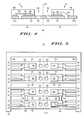
- FIG. 1shows a partial cross-sectional view of a conventional QFP package 10 including a lead frame 11 .
- Lead frame 11includes a flag portion 13 for supporting a semiconductor chip 14 and a lead 16 .
- a wire bond 17connects semiconductor chip 14 to lead 16 .
- An epoxy layer 19covers semiconductor chip 14 and lead frame 11 except for portions of lead 16 , which extend in a gull wing shape from the sides of the package.
- QFP packagestypically are square or rectangular with leads 16 extending from all four sides of the package.
- FIG. 2shows a partial cross-sectional view of a conventional QFN package 20 including lead frame 21 .
- Lead frame 21comprises a flag portion 23 for supporting semiconductor chip 14 , and leads 26 .
- Wire bond 17connects semiconductor chip 14 to a lead 26 .
- Epoxy layer 19covers semiconductor chip 14 and portions of lead frame 21 , while leaving lower portions of flag 23 and lead 26 exposed.
- the leadse.g., lead 26
- the leadsterminate at the edge of the package to provide a smaller package footprint.
- QFN packagestypically are square or rectangular with leads 26 present on all four sides of the lower surface of the package.
- FIG. 3shows an isometric and cut-away view of device 20 .
- the Dual Flat No Lead (DFN) packageis another chip scale package similar to the QFN except that the DFN only has leads on two opposing sides of the lower surface of the package.
- DFNDual Flat No Lead
- QFP, QFN, and DFN packagesincluding large die size to package footprint ratio, matrix lead frame arrays that allow for easier assembly, and established automated assembly tools.
- problems associated with these packagesincluding poor heat transfer capability for high power device applications and very limited mounting options for attaching the packages to next levels of assembly including heat sinks and printed circuit boards.
- lead framese.g., QFP/QFN/DFN platforms
- FIG. 1illustrates a partial cross-sectional view of a prior art Quad Flat Pack (QFP) package
- FIG. 2illustrates a partial cross-sectional view of a prior art Quad Flat Pack No Lead (QFN) package
- FIG. 3illustrates an isometric and cut-away view of the QFN package of FIG. 2 ;
- FIG. 4illustrates a cross-sectional view of a molded array package in accordance with the present invention
- FIG. 5illustrates a partial top view of an assembly structure in accordance with the present invention at an intermediate stage of fabrication
- FIG. 6illustrates a top view of the assembly structure of FIG. 5 during further processing in accordance with the present invention
- FIG. 7illustrates a top view of an outline of a mold cap design for encapsulating the assembly structure of FIG. 5 in accordance with the present invention
- FIG. 8illustrates a top view of the assembly structures of FIGS. 6 and 7 after further processing in accordance with the present invention
- FIG. 9illustrates a top view of a tab mount molded array package in accordance with one embodiment of the present invention.
- FIG. 10illustrates a top view of a tab mount molded array package in accordance with another embodiment of the present invention.
- FIG. 11illustrates a top view of a tab mount molded array package in accordance with a further embodiment of the present invention.
- FIG. 12illustrates a top view of a tab mount molded array package in accordance with still further embodiment of the present invention
- FIG. 13illustrates a cross-sectional view of a molded array package structure in accordance with a further embodiment of the present invention at an intermediate step in fabrication
- FIG. 14illustrates a cross-sectional view of a molded array package structure in accordance with a still further embodiment of the present invention at an intermediate step in fabrication
- FIG. 15illustrates an assembly structure for manufacturing the packages of FIG. 13 and FIG. 14 at an earlier step in fabrication in accordance with the present invention
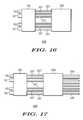
- FIG. 16illustrates a top view of a multi-chip molded array package having a tab mound in accordance with the present invention
- FIG. 17illustrates a top view of a multi-chip molded array package having a tab mount in accordance with another embodiment of the present invention
- FIG. 18illustrates a side view of the multi-chip molded array package of FIG. 17 attached to a next level of assembly in accordance with the present invention
- FIG. 19illustrates a side view of the multi-chip molded array package of FIG. 16 attached to a different next level of assembly in accordance with the present invention
- FIG. 20illustrates a top view of an assembly structure for manufacturing the packages of FIGS. 16 and 17 in accordance with the present invention at an intermediate step in manufacture
- FIG. 21illustrates a top view of the assembly structure of FIG. 20 after further processing in accordance with the present invention.
- FIG. 22illustrates a top view of the assembly structure of FIG. 21 after further processing in accordance with the present invention.
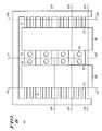
- FIG. 4shows a cross-sectional view of a molded array package, molded structure, flat pack structure, or packaged assembly 40 in accordance with the present invention.
- Packaged assembly 40is shown with two examples of molded devices 41 and 42 . Both devices 41 and 42 include lead frames or conductive lead frames 46 and 47 respectively. Lead frames 46 and 47 each have a flag portion or die attach paddle 51 , which includes an exposed tab 52 .
- Tab 52is an exposed feature or projection that is integral with flag portion 51 , and is provided for attaching devices 41 and 42 to next levels of assembly including, but not limited to, heat sinks, cabinets, printed circuit boards, or the like. In the embodiments shown, exposed tabs 52 are provided with optional through-holes 53 .
- Conductive lead frame 46further includes a conductive lead 57 a that is formed in a no-lead or leadless configuration, which will be explained in more detail below in accordance with the present invention.
- Conductive lead 47includes a conductive lead 57 b that is formed in a leaded or insertion mount configuration, which will be explained in more detail below in accordance with the present invention.
- Devices 41 and 42each include an electronic chip or device 59 attached to flag portions 51 with an attach layer 61 .
- electronic chips 59may comprise power MOSFETS, bipolar power transistors, insulated gate bipolar transistors, thyristors, diodes, sensors, optical devices, and may further include integrated logic devices or other functionality.
- attach layer 61comprises a solder or a high conductivity epoxy material.
- Connective structureselectrically connect electronic chips 59 to the conductive leads.
- a conductive clip or strap 62couples electronic chip of device 41 to conductive lead 57 a
- a wire bond 63couples electronic chip 59 of device 42 to conductive lead 57 b .
- a solder or conductive epoxyis suitable for attaching the clip or strap to lead 57 a and electronic chip 59 .
- An encapsulating layer 66encloses or covers portions of devices 41 and 42 , but does not cover exposed tab portions 52 , through-holes 53 or leads 57 b .
- encapsulating layer 66comprises a plastic epoxy resin material.
- Dashed line 67represents one separation line for singulating devices 41 and 42 into individual devices in a subsequent step.
- FIG. 5shows a partial top view of an assembly structure or sub-assembly 71 in accordance with the present invention at an intermediate stage of fabrication.
- Structure 71includes an array lead frame or main lead frame 72 .
- main lead frame 72comprises a single gauge chemically milled or stamped sheet of a material such as a copper alloy (e.g., TOMAC 4, TAMAC 5, 2ZFROFC, or CDA194), a copper plated iron/nickel alloy (e.g., copper plated Alloy 42 ), plated aluminum, plated plastic, or the like. Plated materials include copper, silver, or multi-layer plating such nickel-palladium and gold.
- main lead frame 72is configured to be compatible with standard quad flat packaging assembly tools.
- Main lead frame 72includes an array or plurality of flags, elongated flag portions, or die attach paddles 51 .
- Electronic chips 59are attached to flag portions 51 , and are further connected or coupled to plurality of leads 57 using, for example, connective wires or wire bonds 63 or conductive clips 62 .
- electronic chips 59are placed onto elongated flags 51 using an automated/programmable pick and place tool. In an early step, a solder paste or epoxy film is placed onto elongated flags 51 to provide attach layer 61 , and electronic chips 59 are then placed onto attach layers 61 .
- main lead frame 72is pre-plated with solder or is pre-coated with a conductive epoxy.
- electronic chips 59include a solder attach layer such as an electroplated Pb/Sn layer or an epoxy layer formed on one surface, and are applied, for example, in wafer form.
- Flag portions 51further include tab portions 52 with through-holes 53 .
- each flag portion 51includes two through-holes 53 , which are on opposite sides of a center line 77 of main lead frame 72 , which is also an example of separation line 67 shown in FIG. 4 .
- leads 57are adjacent outer portions 78 of main lead frame 72 , and main lead frame 72 is formed or provided without, free of, or independent of epoxy mold dam-bars. Additionally, main lead frame 72 is provided or formed so that the top surfaces of leads 57 are substantially co-planar or essentially flat as practical with the top surfaces of flag portions 51 as shown in FIG. 4 .
- coupling devices 79are attached between adjacent flags 51 as shown in FIG. 5 .
- coupling devices 79comprise capacitive devices that provide protection against electrostatic discharge events.
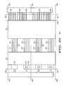
- FIG. 6shows a top view of assembly structure 71 during further processing in accordance with the present invention.
- assembly structure 71is placed in a molding apparatus such as a transfer molding device.
- a solid resin pelletis placed in cull or pot 83 .
- pot 83is heated to melt the solid resin pellet, the liquefied resin material is forced from pot 83 through runners 86 into the slot mold cavities to form a continuous encapsulating layer or encapsulating layer 66 , while leaving portions of leads 57 , tabs 52 and through-holes 53 exposed or un-encapsulated in accordance with an embodiment of the present invention.
- the lower surfacesi.e., the surfaces opposite the surfaces electronic chips 59 are mounted on
- flags 51 and leads 57are not encapsulated to provide electrical contact or connection in subsequent assembly operations.
- FIG. 7shows a top view of an example of an outline of a mold cap design 88 for use with the present invention for forming slot molded array package (MAP) assemblies.
- Mold cap 88includes cavities 89 that hold portions of flags 51 and portions of leads 57 .
- Mold cap 88further includes solid portions 91 that cover or contact other portions of leads 57 and other portions of flags 51 so that these portions are not encapsulated.
- Arrows 92represent an example of a flow direction of encapsulating material during the molding process.
- FIG. 8shows a top view of molded array package assembly 40 in accordance with the present invention that comprises an encapsulated or passivated assembly structure 71 .
- Package assembly 40includes a plurality of exposed leads 57 and a plurality of exposed tabs 52 with through-holes 53 .
- Singulation lines 67 , 103 , 104 , 107 , and 108represent optional separation sites for separating molded array package assembly 40 into separate molded array packages or structures in accordance with the present invention.
- Lines 103are horizontal or first directional cut lines that provide single molded array packages including packages 41 and 42 shown in FIGS. 11 and 12 .
- Line 104is a horizontal or first directional cut line that provides multi-chip molded array packages including packages 410 and 420 shown in FIGS. 9 and 10 .
- Line 67represents a vertical or second directional cut line through elongated flag portions 51 .
- Line 107represents a vertical or second directional cut line that provides a tab mount flat pack no lead molded array package such as packages 420 and 42 shown in FIGS. 10 and 12 .
- Line 108represents a vertical or second directional cut line that provides a tab mount flat pack leaded or single leaded (i.e., leads on one side only) molded array package such as packages 410 and 41 shown in FIGS. 9 and 11 .
- Leaded packages 41 and 410have exposed leads extending outwardly to provide a package style compatible with insertion mount PC board level assembly capabilities.
- Molded array package assembly 40is separated into the possible individual packages described using, for example, conventional dicing, sawing, or laser cutting techniques. Once separated, packages 41 , 42 , 410 , and 420 have singulated encapsulation layers 66 , which are encapsulation layers that have been physically cut through as opposed to cavity molded layers.
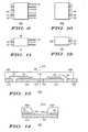
- FIG. 13shows a cross-sectional view of a molded array package, molded structure, flat pack structure, or packaged assembly 400 in accordance with a further embodiment of the present invention.
- Packaged assembly 400is similar to packaged assembly 40 except that elongated flag or die attach paddle 510 does not have horizontal exposed tabs with through-holes because an encapsulating layer 660 covers upper surface 511 of elongated flag 510 .
- encapsulating layer 660is formed with a notch or groove 661 , which after separation along line 670 provides a structure for holding or mounting a clip style heat sink. After separation along line 670 , a vertical exposed tab portion 512 is provided that corresponds to an exposed substantially vertical face of flag portion 510 .
- FIG. 14is a partial cross-sectional view of a molded array package, molded structure, flat pack structure, or packaged assembly 401 in accordance with a still further embodiment of the present invention.
- Packaged assembly 401is similar to packaged assembly 400 except that encapsulating layer 660 does not cover all of upper surface 511 thereby leaving horizontal exposed tab portions 612 .
- Tab portions 612do not include through-holes, and provide for a convenient way to clip the package to a next level of assembly.
- FIG. 15shows a partial top view of an assembly structure or sub-assembly 710 in accordance with the present invention at an intermediate stage of fabrication.
- Structure 710is similar to structure 71 shown in FIG. 5 , except that elongated flags or flag portions 510 (similar structure 5 r in FIG. 5 ) are provided without through-holes.
- Line 670is shown as a vertical separation line as an example of a location for cutting through elongated flag portions 510 after assembly structure 710 is encapsulated using a process similar to that set forth above in conjunction with FIGS. 6-7 .
- FIG. 16shows a top view of an integrated multi-chip molded array package 150 having a separate molded first device or power device portion 151 directly connected to a second molded device portion 152 by conductive leads 157 in accordance with the present invention.
- Molded power device portion 151comprises a single or multiple chip packages similar to packages 41 and 410 shown in FIGS. 9 or 11 , and includes tab portions 52 with through-holes 53 .
- Second molded device portion 152comprises, for example, a molded array packaged logic, sensor, memory, optical circuit device or combination thereof, and is connected to power device portion 151 by exposed or flexible conductive leads 157 extending between the two portions.
- second molded device portion 152further includes leadless connective portions for coupling or connecting to a next level of assembly. Examples of such connective portions are shown as portion 57 a in FIG. 4
- FIG. 17shows a top view of an integrated multi-chip molded array package 160 having a separate molded first device or power device portion 151 directly connected to a second molded device portion 153 by conductive leads 157 in accordance with another embodiment of the present invention.
- Package 160is similar to package 150 except that second molded device portion 153 further includes external, exposed, or outwardly extending conductive leads 158 for connecting or coupling to a next level of assembly.
- Conductive leads 158may be used in place of leadless connective portions (e.g., portions 57 a shown in FIG. 4 ) or in addition thereto.
- Packages 150 and 160 in accordance with the present inventionprovide for a flexible or bendable three dimensional array that is compatible with a variety of heat sinking techniques for power device portion 151 .
- FIG. 18shows a side view of package 150 attached to a next level of assembly 162 in accordance with the present invention.
- leads 157are bent or shaped so that a heat sink device 163 is placed between power device portion 151 and assembly 162 , which provides a way to more effectively cool power device portion 151 .
- Tab portion 52 having through-hole 53provides an attachment means for connecting power device portion 151 to heat sink device 163 .
- a pin, clip, screw 154 or the likeis used for such purposes.
- FIG. 19shows a side view of package 160 attached to a next level of assembly 167 in accordance with the present invention.
- leads 157are bent or shaped so that power device portion 151 is placed adjacent to a vertical heat sink structure or a cabinet 171 .
- Power device portion 151is attached to structure 171 using, for example, a pin, clip, screw 154 or the like.
- FIG. 20shows a partial top view of an assembly structure or sub-assembly 710 for manufacturing the packages of FIGS. 16 and 17 in accordance with the present invention at an intermediate step in manufacture.
- Structure 710includes an array lead frame or main lead frame 720 .
- main lead frame 720comprises a single gauge chemically milled or stamped sheet of a material such as a copper alloy (e.g., TOMAC 4, TAMAC 5, 2ZFROFC, or CDA194), a copper plated iron/nickel alloy (e.g., copper plated Alloy 42 ), plated aluminum, plated plastic, or the like. Plated materials include copper, silver, or multi-layer plating such nickel-palladium and gold.
- a copper alloye.g., TOMAC 4, TAMAC 5, 2ZFROFC, or CDA194
- a copper plated iron/nickel alloye.g., copper plated Alloy 42
- Plated materialsinclude copper, silver, or multi-layer plating such nickel
- Main lead frame 720includes an array or plurality of flag or elongated flag portions 751 .
- First semiconductor devices 759are attached to flag portions 751 , and further connected or coupled to plurality of leads 157 using, for example, wire bonds 763 or conductive clips (not shown).
- First semiconductor devices 759are attached to flag portions 751 using a solder attach layer, a conductive epoxy, or the like, or using an insulative layer, and process such as that described in conjunction with FIG. 5 is suitable for this attachment step.
- devices 759comprise power MOSFETS, insulated gate bipolar transistors, bipolar transistors, thyristors, diodes or the like.
- Elongated flag portions 751further include tab portions 752 having through-holes 753 . In alternative embodiment, tab portions 752 are provided without through-holes 753 as shown in the top portion in FIG. 20 to provide for clip mounting techniques.
- Main lead frame 720further includes an array or plurality of multi chip lead frames 721 , which include a plurality of flags 723 and conductive leads 158 .
- Electronic devices 859 and 959are attached to flags 723 using insulative or conductive attach layers, and connective structures such as wire bonds connect devices 859 and 959 to conductive leads 157 and 158 .
- devices 859 and 959comprise sensor, optical, logic, control, or memory devices, combinations thereof, or the like.
- Components 1059such as capacitive components may be used between adjacent conductive leads to provide, for example, circuit protection from electrostatic discharge events.
- FIG. 21shows a top view of assembly structure 710 during further processing in accordance with the present invention.
- assembly structure 710is placed in a molding apparatus such as a transfer molding device.
- a solid resin pelletis placed in cull or pot 783 .
- pot 783is heated to melt the solid resin pellet, the liquefied resin material is forced from pot 783 through runners 786 into the slot mold cavities to form encapsulating layers 766 , while leaving portions of leads 157 and 158 and tab portions 752 with through-holes 753 exposed in accordance with the present invention.
- the lower surfaces of flags 751 and/or 723 and the lower surfaces of leads 158are not encapsulated.
- FIG. 22shows a top view of integrated multi-chip molded array package structure 810 having tabs 752 with through-holes 753 in accordance with the present invention prior to separation.
- Singulation lines 803 , 804 , 806 , and 807represent examples of separation locations for separating structure 810 into separate multi-chip molded array packages.
- Lines 803are horizontal or first directional cut lines for separating individual packages and pass through molded portions of the devices.
- Line 804is a vertical or second directional cut line for separating tab portions 752 from the main lead frame.
- Optional cut line 806is a vertical or second directional cut line that provides a no-lead or leadless embodiment such as that shown in FIG. 16 in accordance with the present invention.
- Optional cut line 807is a vertical or second directional cut line that provides a leaded embodiment such as that shown in FIG. 17 in accordance with the present invention.
- a structure and method for forming molded array package having an exposed tab with a through-holeprovide optional embodiment flexibility including no-lead devices, leaded devices, and multiple-chip devices including devices having multiple molded portions with leaded interconnects.
- the exposed leads of devices according to the present inventionmay be flat or bent or shaped (e.g., gull wing shaped) at various angles according to assembly requirements.
Landscapes
- Engineering & Computer Science (AREA)
- Computer Hardware Design (AREA)
- Microelectronics & Electronic Packaging (AREA)
- Power Engineering (AREA)
- Physics & Mathematics (AREA)
- Condensed Matter Physics & Semiconductors (AREA)
- General Physics & Mathematics (AREA)
- Manufacturing & Machinery (AREA)
- Structures Or Materials For Encapsulating Or Coating Semiconductor Devices Or Solid State Devices (AREA)
- Lead Frames For Integrated Circuits (AREA)
Abstract
Description
- This invention relates generally to electronic devices, and more specifically to power semiconductor packages and methods of assembly.
- The handheld consumer products market is aggressive in the miniaturization of portable electronics. Primarily driven at present by the cellular phone and digital assistant markets, manufacturers of these devices are challenged by ever shrinking formats and the demand for more PC-like functionality. This challenge asserts pressure on surface mount component manufacturers to design their products to command the smallest area possible. By doing so, this allows portable electronics designers to incorporate additional functions within a device without increasing the overall product size.
- In Chip Scale Packaging (CSP) technologies, manufacturers strive to bring the package size as close as possible to the size of the semiconductor chip. The electronics industry has accepted the Joint Electronic Device Engineering Council (JEDEC) defined Quad Flat Pack (QFP) and Quad Flat Pack No Lead (QFN) outlines as good alternatives for low cost chip scale packages. In typical QFP and QFN packages, the lower surface of a semiconductor chip is attached to a metal lead frame. Wire bonds are then used to connect circuitry located on the front side of the chip to individual leads on the lead frame. The chip and lead frame are subsequently encapsulated by an epoxy resin to form an assembled component.
FIG. 1 shows a partial cross-sectional view of aconventional QFP package 10 including alead frame 11.Lead frame 11 includes aflag portion 13 for supporting asemiconductor chip 14 and alead 16. Awire bond 17 connectssemiconductor chip 14 to lead16. Anepoxy layer 19 coverssemiconductor chip 14 andlead frame 11 except for portions oflead 16, which extend in a gull wing shape from the sides of the package. Although only a portion ofQFP package 10 is shown, QFP packages typically are square or rectangular withleads 16 extending from all four sides of the package.FIG. 2 shows a partial cross-sectional view of aconventional QFN package 20 includinglead frame 21.Lead frame 21 comprises aflag portion 23 for supportingsemiconductor chip 14, and leads26. Wirebond 17 connectssemiconductor chip 14 to alead 26. Epoxylayer 19 coverssemiconductor chip 14 and portions oflead frame 21, while leaving lower portions offlag 23 andlead 26 exposed. In the QFN package, the leads (e.g., lead26) terminate at the edge of the package to provide a smaller package footprint. Although only a portion ofQFN package 20 is shown, QFN packages typically are square or rectangular withleads 26 present on all four sides of the lower surface of the package.FIG. 3 shows an isometric and cut-away view ofdevice 20. The Dual Flat No Lead (DFN) package is another chip scale package similar to the QFN except that the DFN only has leads on two opposing sides of the lower surface of the package.- There are several advantages to QFP, QFN, and DFN packages including large die size to package footprint ratio, matrix lead frame arrays that allow for easier assembly, and established automated assembly tools. However, there are several problems associated with these packages including poor heat transfer capability for high power device applications and very limited mounting options for attaching the packages to next levels of assembly including heat sinks and printed circuit boards.
- Accordingly, a need exists for a package structure and method of assembly that is manufacturable on existing chip scale assembly platforms that use lead frames (e.g., QFP/QFN/DFN platforms), that supports high power applications, that supports multiple die options, and that has more flexible attachment options for connecting to next levels of assembly.
FIG. 1 illustrates a partial cross-sectional view of a prior art Quad Flat Pack (QFP) package;FIG. 2 illustrates a partial cross-sectional view of a prior art Quad Flat Pack No Lead (QFN) package;FIG. 3 illustrates an isometric and cut-away view of the QFN package ofFIG. 2 ;FIG. 4 illustrates a cross-sectional view of a molded array package in accordance with the present invention;FIG. 5 illustrates a partial top view of an assembly structure in accordance with the present invention at an intermediate stage of fabrication;FIG. 6 illustrates a top view of the assembly structure ofFIG. 5 during further processing in accordance with the present invention;FIG. 7 illustrates a top view of an outline of a mold cap design for encapsulating the assembly structure ofFIG. 5 in accordance with the present invention;FIG. 8 illustrates a top view of the assembly structures ofFIGS. 6 and 7 after further processing in accordance with the present invention;FIG. 9 illustrates a top view of a tab mount molded array package in accordance with one embodiment of the present invention;FIG. 10 illustrates a top view of a tab mount molded array package in accordance with another embodiment of the present invention;FIG. 11 illustrates a top view of a tab mount molded array package in accordance with a further embodiment of the present invention;FIG. 12 illustrates a top view of a tab mount molded array package in accordance with still further embodiment of the present invention;FIG. 13 illustrates a cross-sectional view of a molded array package structure in accordance with a further embodiment of the present invention at an intermediate step in fabrication;FIG. 14 illustrates a cross-sectional view of a molded array package structure in accordance with a still further embodiment of the present invention at an intermediate step in fabrication;FIG. 15 illustrates an assembly structure for manufacturing the packages ofFIG. 13 andFIG. 14 at an earlier step in fabrication in accordance with the present invention;FIG. 16 illustrates a top view of a multi-chip molded array package having a tab mound in accordance with the present invention;FIG. 17 illustrates a top view of a multi-chip molded array package having a tab mount in accordance with another embodiment of the present invention;FIG. 18 illustrates a side view of the multi-chip molded array package ofFIG. 17 attached to a next level of assembly in accordance with the present invention;FIG. 19 illustrates a side view of the multi-chip molded array package ofFIG. 16 attached to a different next level of assembly in accordance with the present invention;FIG. 20 illustrates a top view of an assembly structure for manufacturing the packages ofFIGS. 16 and 17 in accordance with the present invention at an intermediate step in manufacture;FIG. 21 illustrates a top view of the assembly structure ofFIG. 20 after further processing in accordance with the present invention; andFIG. 22 illustrates a top view of the assembly structure ofFIG. 21 after further processing in accordance with the present invention.- For ease of understanding, elements in the drawing figures are not necessarily drawn to scale, and like element numbers are used where appropriate throughout the various figures to denote the same or similar elements.
FIG. 4 shows a cross-sectional view of a molded array package, molded structure, flat pack structure, or packagedassembly 40 in accordance with the present invention. Packagedassembly 40 is shown with two examples ofmolded devices devices conductive lead frames Lead frames attach paddle 51, which includes an exposedtab 52.Tab 52 is an exposed feature or projection that is integral withflag portion 51, and is provided for attachingdevices tabs 52 are provided with optional through-holes 53.Conductive lead frame 46 further includes aconductive lead 57athat is formed in a no-lead or leadless configuration, which will be explained in more detail below in accordance with the present invention.Conductive lead 47 includes aconductive lead 57bthat is formed in a leaded or insertion mount configuration, which will be explained in more detail below in accordance with the present invention.Devices device 59 attached toflag portions 51 with anattach layer 61. By way of example,electronic chips 59 may comprise power MOSFETS, bipolar power transistors, insulated gate bipolar transistors, thyristors, diodes, sensors, optical devices, and may further include integrated logic devices or other functionality. By way of further example,attach layer 61 comprises a solder or a high conductivity epoxy material.- Connective structures electrically connect
electronic chips 59 to the conductive leads. For example, a conductive clip or strap62 couples electronic chip ofdevice 41 toconductive lead 57a, and awire bond 63 coupleselectronic chip 59 ofdevice 42 toconductive lead 57b. When a clip or strap is used, a solder or conductive epoxy is suitable for attaching the clip or strap to lead57aandelectronic chip 59. - An
encapsulating layer 66 encloses or covers portions ofdevices tab portions 52, through-holes 53 or leads57b. By way of example, encapsulatinglayer 66 comprises a plastic epoxy resin material. Dashedline 67 represents one separation line forsingulating devices FIG. 5 shows a partial top view of an assembly structure orsub-assembly 71 in accordance with the present invention at an intermediate stage of fabrication.Structure 71 includes an array lead frame ormain lead frame 72. By way of example,main lead frame 72 comprises a single gauge chemically milled or stamped sheet of a material such as a copper alloy (e.g., TOMAC 4,TAMAC 5, 2ZFROFC, or CDA194), a copper plated iron/nickel alloy (e.g., copper plated Alloy42), plated aluminum, plated plastic, or the like. Plated materials include copper, silver, or multi-layer plating such nickel-palladium and gold. Again by way of example,main lead frame 72 is configured to be compatible with standard quad flat packaging assembly tools.Main lead frame 72 includes an array or plurality of flags, elongated flag portions, or die attachpaddles 51.Electronic chips 59 are attached to flagportions 51, and are further connected or coupled to plurality ofleads 57 using, for example, connective wires orwire bonds 63 orconductive clips 62. By way of example,electronic chips 59 are placed ontoelongated flags 51 using an automated/programmable pick and place tool. In an early step, a solder paste or epoxy film is placed ontoelongated flags 51 to provide attachlayer 61, andelectronic chips 59 are then placed onto attach layers61. The assembly is then placed through a curing process to cure or reflow attachlayer 61 to form a conductive bond betweenelectronic chip 59 andelongated flag portion 51. Alternatively,main lead frame 72 is pre-plated with solder or is pre-coated with a conductive epoxy. Optionally,electronic chips 59 include a solder attach layer such as an electroplated Pb/Sn layer or an epoxy layer formed on one surface, and are applied, for example, in wafer form.Flag portions 51 further includetab portions 52 with through-holes 53. In one embodiment, eachflag portion 51 includes two through-holes 53, which are on opposite sides of acenter line 77 ofmain lead frame 72, which is also an example ofseparation line 67 shown inFIG. 4 . In one embodiment, leads57 are adjacentouter portions 78 ofmain lead frame 72, andmain lead frame 72 is formed or provided without, free of, or independent of epoxy mold dam-bars. Additionally,main lead frame 72 is provided or formed so that the top surfaces ofleads 57 are substantially co-planar or essentially flat as practical with the top surfaces offlag portions 51 as shown inFIG. 4 . In an optional embodiment,coupling devices 79 are attached betweenadjacent flags 51 as shown inFIG. 5 . By way of example,coupling devices 79 comprise capacitive devices that provide protection against electrostatic discharge events.FIG. 6 shows a top view ofassembly structure 71 during further processing in accordance with the present invention. In this step,assembly structure 71 is placed in a molding apparatus such as a transfer molding device. A solid resin pellet is placed in cull orpot 83. Whenpot 83 is heated to melt the solid resin pellet, the liquefied resin material is forced frompot 83 throughrunners 86 into the slot mold cavities to form a continuous encapsulating layer or encapsulatinglayer 66, while leaving portions ofleads 57,tabs 52 and through-holes 53 exposed or un-encapsulated in accordance with an embodiment of the present invention. It is understood that in one embodiment, the lower surfaces (i.e., the surfaces opposite the surfaceselectronic chips 59 are mounted on) offlags 51 and leads57 are not encapsulated to provide electrical contact or connection in subsequent assembly operations.FIG. 7 shows a top view of an example of an outline of amold cap design 88 for use with the present invention for forming slot molded array package (MAP) assemblies.Mold cap 88 includescavities 89 that hold portions offlags 51 and portions of leads57.Mold cap 88 further includessolid portions 91 that cover or contact other portions ofleads 57 and other portions offlags 51 so that these portions are not encapsulated.Arrows 92 represent an example of a flow direction of encapsulating material during the molding process.FIG. 8 shows a top view of moldedarray package assembly 40 in accordance with the present invention that comprises an encapsulated or passivatedassembly structure 71.Package assembly 40 includes a plurality of exposed leads57 and a plurality of exposedtabs 52 with through-holes 53. Singulation lines67,103,104,107, and108 represent optional separation sites for separating moldedarray package assembly 40 into separate molded array packages or structures in accordance with the present invention.Lines 103 are horizontal or first directional cut lines that provide single molded arraypackages including packages FIGS. 11 and 12 .Line 104 is a horizontal or first directional cut line that provides multi-chip molded arraypackages including packages FIGS. 9 and 10 .Line 67 represents a vertical or second directional cut line throughelongated flag portions 51.Line 107 represents a vertical or second directional cut line that provides a tab mount flat pack no lead molded array package such aspackages FIGS. 10 and 12 .Line 108 represents a vertical or second directional cut line that provides a tab mount flat pack leaded or single leaded (i.e., leads on one side only) molded array package such aspackages FIGS. 9 and 11 .Leaded packages array package assembly 40 is separated into the possible individual packages described using, for example, conventional dicing, sawing, or laser cutting techniques. Once separated, packages41,42,410, and420 have singulated encapsulation layers66, which are encapsulation layers that have been physically cut through as opposed to cavity molded layers.FIG. 13 shows a cross-sectional view of a molded array package, molded structure, flat pack structure, or packagedassembly 400 in accordance with a further embodiment of the present invention. Packagedassembly 400 is similar to packagedassembly 40 except that elongated flag or die attachpaddle 510 does not have horizontal exposed tabs with through-holes because anencapsulating layer 660 coversupper surface 511 ofelongated flag 510. In an optional embodiment, encapsulatinglayer 660 is formed with a notch or groove661, which after separation alongline 670 provides a structure for holding or mounting a clip style heat sink. After separation alongline 670, a vertical exposedtab portion 512 is provided that corresponds to an exposed substantially vertical face offlag portion 510.FIG. 14 is a partial cross-sectional view of a molded array package, molded structure, flat pack structure, or packagedassembly 401 in accordance with a still further embodiment of the present invention. Packagedassembly 401 is similar to packagedassembly 400 except that encapsulatinglayer 660 does not cover all ofupper surface 511 thereby leaving horizontal exposedtab portions 612.Tab portions 612 do not include through-holes, and provide for a convenient way to clip the package to a next level of assembly.FIG. 15 shows a partial top view of an assembly structure or sub-assembly710 in accordance with the present invention at an intermediate stage of fabrication.Structure 710 is similar to structure71 shown inFIG. 5 , except that elongated flags or flag portions510 (similar structure5rinFIG. 5 ) are provided without through-holes.Line 670 is shown as a vertical separation line as an example of a location for cutting throughelongated flag portions 510 afterassembly structure 710 is encapsulated using a process similar to that set forth above in conjunction withFIGS. 6-7 .FIG. 16 shows a top view of an integrated multi-chip moldedarray package 150 having a separate molded first device orpower device portion 151 directly connected to a second moldeddevice portion 152 byconductive leads 157 in accordance with the present invention. Moldedpower device portion 151 comprises a single or multiple chip packages similar topackages tab portions 52 with through-holes 53. Second moldeddevice portion 152 comprises, for example, a molded array packaged logic, sensor, memory, optical circuit device or combination thereof, and is connected topower device portion 151 by exposed or flexible conductive leads157 extending between the two portions. In this embodiment, second moldeddevice portion 152 further includes leadless connective portions for coupling or connecting to a next level of assembly. Examples of such connective portions are shown asportion 57ainFIG. 4 FIG. 17 shows a top view of an integrated multi-chip moldedarray package 160 having a separate molded first device orpower device portion 151 directly connected to a second moldeddevice portion 153 byconductive leads 157 in accordance with another embodiment of the present invention.Package 160 is similar to package150 except that second moldeddevice portion 153 further includes external, exposed, or outwardly extendingconductive leads 158 for connecting or coupling to a next level of assembly. Conductive leads158 may be used in place of leadless connective portions (e.g.,portions 57ashown inFIG. 4 ) or in addition thereto.Packages power device portion 151. For example,FIG. 18 shows a side view ofpackage 150 attached to a next level ofassembly 162 in accordance with the present invention. In this embodiment, leads157 are bent or shaped so that aheat sink device 163 is placed betweenpower device portion 151 andassembly 162, which provides a way to more effectively coolpower device portion 151.Tab portion 52 having through-hole 53 provides an attachment means for connectingpower device portion 151 toheat sink device 163. By way of example, a pin, clip, screw154 or the like is used for such purposes.FIG. 19 shows a side view ofpackage 160 attached to a next level of assembly167 in accordance with the present invention. In this embodiment, leads157 are bent or shaped so thatpower device portion 151 is placed adjacent to a vertical heat sink structure or acabinet 171.Power device portion 151 is attached to structure171 using, for example, a pin, clip, screw154 or the like.FIG. 20 shows a partial top view of an assembly structure or sub-assembly710 for manufacturing the packages ofFIGS. 16 and 17 in accordance with the present invention at an intermediate step in manufacture. The layout example shown is compatible with quad flat packaging assembly techniques.Structure 710 includes an array lead frame or mainlead frame 720. By way of example,main lead frame 720 comprises a single gauge chemically milled or stamped sheet of a material such as a copper alloy (e.g., TOMAC 4,TAMAC 5, 2ZFROFC, or CDA194), a copper plated iron/nickel alloy (e.g., copper plated Alloy42), plated aluminum, plated plastic, or the like. Plated materials include copper, silver, or multi-layer plating such nickel-palladium and gold.- Main
lead frame 720 includes an array or plurality of flag orelongated flag portions 751.First semiconductor devices 759 are attached to flagportions 751, and further connected or coupled to plurality ofleads 157 using, for example,wire bonds 763 or conductive clips (not shown).First semiconductor devices 759 are attached to flagportions 751 using a solder attach layer, a conductive epoxy, or the like, or using an insulative layer, and process such as that described in conjunction withFIG. 5 is suitable for this attachment step. By way of example,devices 759 comprise power MOSFETS, insulated gate bipolar transistors, bipolar transistors, thyristors, diodes or the like.Elongated flag portions 751 further includetab portions 752 having through-holes 753. In alternative embodiment,tab portions 752 are provided without through-holes 753 as shown in the top portion inFIG. 20 to provide for clip mounting techniques. - Main
lead frame 720 further includes an array or plurality of multi chip lead frames721, which include a plurality offlags 723 and conductive leads158.Electronic devices flags 723 using insulative or conductive attach layers, and connective structures such as wire bonds connectdevices conductive leads devices Components 1059 such as capacitive components may be used between adjacent conductive leads to provide, for example, circuit protection from electrostatic discharge events. FIG. 21 shows a top view ofassembly structure 710 during further processing in accordance with the present invention. In this step,assembly structure 710 is placed in a molding apparatus such as a transfer molding device. A solid resin pellet is placed in cull orpot 783. Whenpot 783 is heated to melt the solid resin pellet, the liquefied resin material is forced frompot 783 throughrunners 786 into the slot mold cavities to form encapsulatinglayers 766, while leaving portions ofleads tab portions 752 with through-holes 753 exposed in accordance with the present invention. It is understood that in one embodiment, the lower surfaces offlags 751 and/or723 and the lower surfaces ofleads 158 are not encapsulated.FIG. 22 shows a top view of integrated multi-chip molded array package structure810 havingtabs 752 with through-holes 753 in accordance with the present invention prior to separation. Singulation lines803,804,806, and807 represent examples of separation locations for separating structure810 into separate multi-chip molded array packages.Lines 803 are horizontal or first directional cut lines for separating individual packages and pass through molded portions of the devices.Line 804 is a vertical or second directional cut line for separatingtab portions 752 from the main lead frame. Optional cut line806 is a vertical or second directional cut line that provides a no-lead or leadless embodiment such as that shown inFIG. 16 in accordance with the present invention.Optional cut line 807 is a vertical or second directional cut line that provides a leaded embodiment such as that shown inFIG. 17 in accordance with the present invention.- Thus, it is apparent that there has been provided, in accordance with the present invention, a structure and method for forming molded array package having an exposed tab with a through-hole. The package and method provide optional embodiment flexibility including no-lead devices, leaded devices, and multiple-chip devices including devices having multiple molded portions with leaded interconnects.
- Although the invention has been described and illustrated with reference to specific embodiments thereof, it is not intended that the invention be limited to these illustrative embodiments. For example, the exposed leads of devices according to the present invention may be flat or bent or shaped (e.g., gull wing shaped) at various angles according to assembly requirements.
Claims (24)
Priority Applications (5)
| Application Number | Priority Date | Filing Date | Title |
|---|---|---|---|
| US11/243,195US7602054B2 (en) | 2005-10-05 | 2005-10-05 | Method of forming a molded array package device having an exposed tab and structure |
| MYPI20064060AMY141183A (en) | 2005-10-05 | 2006-08-30 | Method of forming a molded array package device having an exposed tab and structure |
| CNB2006101540464ACN100543952C (en) | 2005-10-05 | 2006-09-20 | Making has the method and structure of the molded array package device of the fin that exposes |
| HK07109951.1AHK1104674B (en) | 2005-10-05 | 2007-09-13 | Method of forming a molded array package device having an exposed tab and structure |
| US12/553,706US7901990B2 (en) | 2005-10-05 | 2009-09-03 | Method of forming a molded array package device having an exposed tab and structure |
Applications Claiming Priority (1)
| Application Number | Priority Date | Filing Date | Title |
|---|---|---|---|
| US11/243,195US7602054B2 (en) | 2005-10-05 | 2005-10-05 | Method of forming a molded array package device having an exposed tab and structure |
Related Child Applications (1)
| Application Number | Title | Priority Date | Filing Date |
|---|---|---|---|
| US12/553,706DivisionUS7901990B2 (en) | 2005-10-05 | 2009-09-03 | Method of forming a molded array package device having an exposed tab and structure |
Publications (2)
| Publication Number | Publication Date |
|---|---|
| US20070075409A1true US20070075409A1 (en) | 2007-04-05 |
| US7602054B2 US7602054B2 (en) | 2009-10-13 |
Family
ID=37901107
Family Applications (2)
| Application Number | Title | Priority Date | Filing Date |
|---|---|---|---|
| US11/243,195Active2028-05-03US7602054B2 (en) | 2005-10-05 | 2005-10-05 | Method of forming a molded array package device having an exposed tab and structure |
| US12/553,706Expired - LifetimeUS7901990B2 (en) | 2005-10-05 | 2009-09-03 | Method of forming a molded array package device having an exposed tab and structure |
Family Applications After (1)
| Application Number | Title | Priority Date | Filing Date |
|---|---|---|---|
| US12/553,706Expired - LifetimeUS7901990B2 (en) | 2005-10-05 | 2009-09-03 | Method of forming a molded array package device having an exposed tab and structure |
Country Status (3)
| Country | Link |
|---|---|
| US (2) | US7602054B2 (en) |
| CN (1) | CN100543952C (en) |
| MY (1) | MY141183A (en) |
Cited By (20)
| Publication number | Priority date | Publication date | Assignee | Title |
|---|---|---|---|---|
| US20070040187A1 (en)* | 2005-08-16 | 2007-02-22 | Nobuya Koike | Semiconductor device and manufacturing method of the same |
| US20070111393A1 (en)* | 2005-10-28 | 2007-05-17 | Semiconductor Components Industries, Llc | Method of forming a leaded molded array package |
| US20090026590A1 (en)* | 2007-07-23 | 2009-01-29 | National Semiconductor Corporation | Leadframe panel |
| US20090218666A1 (en)* | 2008-02-28 | 2009-09-03 | Yang Gwi-Gyeon | Power device package and method of fabricating the same |
| US20100038759A1 (en)* | 2008-08-13 | 2010-02-18 | Atmel Corporation | Leadless Package with Internally Extended Package Leads |
| US7763958B1 (en)* | 2007-05-25 | 2010-07-27 | National Semiconductor Corporation | Leadframe panel for power packages |
| WO2011015642A1 (en)* | 2009-08-05 | 2011-02-10 | Continental Teves Ag & Co. Ohg | Sensor arrangement and chip comprising additional fixing pins |
| US20110109287A1 (en)* | 2009-11-09 | 2011-05-12 | Kabushiki Kaisha Toshiba | Semiconductor package and dc-dc converter |
| US20120092832A1 (en)* | 2010-10-19 | 2012-04-19 | Tessera Research Llc | Enhanced stacked microelectronic assemblies with central contacts and improved thermal characteristics |
| US8455987B1 (en)* | 2009-06-16 | 2013-06-04 | Ixys Corporation | Electrically isolated power semiconductor package with optimized layout |
| US8928153B2 (en) | 2011-04-21 | 2015-01-06 | Tessera, Inc. | Flip-chip, face-up and face-down centerbond memory wirebond assemblies |
| US8952516B2 (en) | 2011-04-21 | 2015-02-10 | Tessera, Inc. | Multiple die stacking for two or more die |
| US8970028B2 (en) | 2011-12-29 | 2015-03-03 | Invensas Corporation | Embedded heat spreader for package with multiple microelectronic elements and face-down connection |
| US9013033B2 (en) | 2011-04-21 | 2015-04-21 | Tessera, Inc. | Multiple die face-down stacking for two or more die |
| US9093291B2 (en) | 2011-04-21 | 2015-07-28 | Tessera, Inc. | Flip-chip, face-up and face-down wirebond combination package |
| US9281266B2 (en) | 2011-04-21 | 2016-03-08 | Tessera, Inc. | Stacked chip-on-board module with edge connector |
| US20160322286A1 (en)* | 2014-01-09 | 2016-11-03 | Hitachi Automotive Systems, Ltd. | Semiconductor Device and Power Converter Using the Same |
| US9941224B2 (en)* | 2016-08-24 | 2018-04-10 | Allegro Microsystems, Llc | Multi-die integrated circuit device with capacitive overvoltage protection |
| US10145904B2 (en) | 2016-08-24 | 2018-12-04 | Allegro Microsystems, Llc | Multi-die integrated circuit device with overvoltage protection |
| US10147688B2 (en) | 2016-02-25 | 2018-12-04 | Allegro Microsystems, Llc | Integrated circuit device with overvoltage discharge protection |
Families Citing this family (3)
| Publication number | Priority date | Publication date | Assignee | Title |
|---|---|---|---|---|
| FR3018630A1 (en)* | 2014-03-11 | 2015-09-18 | St Microelectronics Grenoble 2 | PERFORATED ELECTRONIC HOUSING AND METHOD OF MANUFACTURE |
| US9583421B2 (en) | 2015-07-16 | 2017-02-28 | Semiconductor Components Industries, Llc | Recessed lead leadframe packages |
| US9966652B2 (en)* | 2015-11-03 | 2018-05-08 | Amkor Technology, Inc. | Packaged electronic device having integrated antenna and locking structure |
Citations (8)
| Publication number | Priority date | Publication date | Assignee | Title |
|---|---|---|---|---|
| US3581387A (en)* | 1967-11-29 | 1971-06-01 | Gen Motors Corp | Method of making strip mounted semiconductor device |
| US4012765A (en)* | 1975-09-24 | 1977-03-15 | Motorola, Inc. | Lead frame for plastic encapsulated semiconductor assemblies |
| US4451973A (en)* | 1981-04-28 | 1984-06-05 | Matsushita Electronics Corporation | Method for manufacturing a plastic encapsulated semiconductor device and a lead frame therefor |
| US4641418A (en)* | 1982-08-30 | 1987-02-10 | International Rectifier Corporation | Molding process for semiconductor devices and lead frame structure therefor |
| US5661342A (en)* | 1994-11-09 | 1997-08-26 | Mitsubishi Denki Kabushiki Kaisha | Semiconductor device with heat sink including positioning pins |
| US6465875B2 (en)* | 2000-03-27 | 2002-10-15 | International Rectifier Corporation | Semiconductor device package with plural pad lead frame |
| US7005728B1 (en)* | 2004-06-03 | 2006-02-28 | National Semiconductor Corporation | Lead configuration for inline packages |
| US7342297B1 (en)* | 2004-04-22 | 2008-03-11 | National Semiconductor Corporation | Sawn power package |
Family Cites Families (7)
| Publication number | Priority date | Publication date | Assignee | Title |
|---|---|---|---|---|
| US4043027A (en)* | 1963-12-16 | 1977-08-23 | Texas Instruments Incorporated | Process for encapsulating electronic components in plastic |
| JPS62122136A (en)* | 1985-11-08 | 1987-06-03 | Hitachi Ltd | Resin molded semiconductor manufacturing method and device |
| JPH05299456A (en)* | 1992-04-20 | 1993-11-12 | Toshiba Corp | Semiconductor device sealed with resin |
| US5659950A (en)* | 1995-03-23 | 1997-08-26 | Motorola, Inc. | Method of forming a package assembly |
| CN1179626A (en)* | 1996-09-05 | 1998-04-22 | 国际整流器公司 | Improved surface-mount high power semiconductor package and method of manufacture |
| JP3416942B2 (en)* | 1997-09-25 | 2003-06-16 | 住友電気工業株式会社 | Optical module and lead frame for optical module |
| JP3510838B2 (en)* | 2000-03-24 | 2004-03-29 | 三洋電機株式会社 | Semiconductor device and manufacturing method thereof |
- 2005
- 2005-10-05USUS11/243,195patent/US7602054B2/enactiveActive
- 2006
- 2006-08-30MYMYPI20064060Apatent/MY141183A/enunknown
- 2006-09-20CNCNB2006101540464Apatent/CN100543952C/enactiveActive
- 2009
- 2009-09-03USUS12/553,706patent/US7901990B2/ennot_activeExpired - Lifetime
Patent Citations (8)
| Publication number | Priority date | Publication date | Assignee | Title |
|---|---|---|---|---|
| US3581387A (en)* | 1967-11-29 | 1971-06-01 | Gen Motors Corp | Method of making strip mounted semiconductor device |
| US4012765A (en)* | 1975-09-24 | 1977-03-15 | Motorola, Inc. | Lead frame for plastic encapsulated semiconductor assemblies |
| US4451973A (en)* | 1981-04-28 | 1984-06-05 | Matsushita Electronics Corporation | Method for manufacturing a plastic encapsulated semiconductor device and a lead frame therefor |
| US4641418A (en)* | 1982-08-30 | 1987-02-10 | International Rectifier Corporation | Molding process for semiconductor devices and lead frame structure therefor |
| US5661342A (en)* | 1994-11-09 | 1997-08-26 | Mitsubishi Denki Kabushiki Kaisha | Semiconductor device with heat sink including positioning pins |
| US6465875B2 (en)* | 2000-03-27 | 2002-10-15 | International Rectifier Corporation | Semiconductor device package with plural pad lead frame |
| US7342297B1 (en)* | 2004-04-22 | 2008-03-11 | National Semiconductor Corporation | Sawn power package |
| US7005728B1 (en)* | 2004-06-03 | 2006-02-28 | National Semiconductor Corporation | Lead configuration for inline packages |
Cited By (45)
| Publication number | Priority date | Publication date | Assignee | Title |
|---|---|---|---|---|
| US7968370B2 (en) | 2005-08-16 | 2011-06-28 | Renesas Electronics Corporation | Semiconductor connection component |
| US7462887B2 (en)* | 2005-08-16 | 2008-12-09 | Renesas Technology Corp. | Semiconductor connection component |
| US20110143500A1 (en)* | 2005-08-16 | 2011-06-16 | Renesas Electronics Corporation | Semiconductor connection component |
| US20090068796A1 (en)* | 2005-08-16 | 2009-03-12 | Renesas Technology Corp. | Semiconductor connection component |
| US20070040187A1 (en)* | 2005-08-16 | 2007-02-22 | Nobuya Koike | Semiconductor device and manufacturing method of the same |
| US8298859B2 (en) | 2005-08-16 | 2012-10-30 | Renesas Electronics Corporation | Semiconductor connection component |
| US20070111393A1 (en)* | 2005-10-28 | 2007-05-17 | Semiconductor Components Industries, Llc | Method of forming a leaded molded array package |
| US7588999B2 (en)* | 2005-10-28 | 2009-09-15 | Semiconductor Components Industries, Llc | Method of forming a leaded molded array package |
| US7763958B1 (en)* | 2007-05-25 | 2010-07-27 | National Semiconductor Corporation | Leadframe panel for power packages |
| US7714418B2 (en) | 2007-07-23 | 2010-05-11 | National Semiconductor Corporation | Leadframe panel |
| US20090026590A1 (en)* | 2007-07-23 | 2009-01-29 | National Semiconductor Corporation | Leadframe panel |
| US8198139B2 (en)* | 2008-02-28 | 2012-06-12 | Fairchild Korea Semiconductor Ltd. | Power device package and method of fabricating the same |
| US20090218666A1 (en)* | 2008-02-28 | 2009-09-03 | Yang Gwi-Gyeon | Power device package and method of fabricating the same |
| US8174099B2 (en) | 2008-08-13 | 2012-05-08 | Atmel Corporation | Leadless package with internally extended package leads |
| US20100038759A1 (en)* | 2008-08-13 | 2010-02-18 | Atmel Corporation | Leadless Package with Internally Extended Package Leads |
| US8455987B1 (en)* | 2009-06-16 | 2013-06-04 | Ixys Corporation | Electrically isolated power semiconductor package with optimized layout |
| US9177888B2 (en)* | 2009-06-16 | 2015-11-03 | Ixys Corporation | Electrically isolated power semiconductor package with optimized layout |
| US8901723B2 (en) | 2009-06-16 | 2014-12-02 | Ixys Corporation | Electrically isolated power semiconductor package with optimized layout |
| US20150087113A1 (en)* | 2009-06-16 | 2015-03-26 | Ixys Corporation | Electrically isolated power semiconductor package with optimized layout |
| US9640467B2 (en) | 2009-08-05 | 2017-05-02 | Continental Teves Ag & Co. Ohg | Sensor arrangement and chip comprising additional fixing pins |
| WO2011015642A1 (en)* | 2009-08-05 | 2011-02-10 | Continental Teves Ag & Co. Ohg | Sensor arrangement and chip comprising additional fixing pins |
| US20110109287A1 (en)* | 2009-11-09 | 2011-05-12 | Kabushiki Kaisha Toshiba | Semiconductor package and dc-dc converter |
| US8941999B2 (en) | 2010-10-19 | 2015-01-27 | Tessera, Inc. | Enhanced stacked microelectronic assemblies with central contacts and improved thermal characteristics |
| US8553420B2 (en)* | 2010-10-19 | 2013-10-08 | Tessera, Inc. | Enhanced stacked microelectronic assemblies with central contacts and improved thermal characteristics |
| US20120092832A1 (en)* | 2010-10-19 | 2012-04-19 | Tessera Research Llc | Enhanced stacked microelectronic assemblies with central contacts and improved thermal characteristics |
| US9312239B2 (en) | 2010-10-19 | 2016-04-12 | Tessera, Inc. | Enhanced stacked microelectronic assemblies with central contacts and improved thermal characteristics |
| US9437579B2 (en) | 2011-04-21 | 2016-09-06 | Tessera, Inc. | Multiple die face-down stacking for two or more die |
| US9806017B2 (en) | 2011-04-21 | 2017-10-31 | Tessera, Inc. | Flip-chip, face-up and face-down centerbond memory wirebond assemblies |
| US9013033B2 (en) | 2011-04-21 | 2015-04-21 | Tessera, Inc. | Multiple die face-down stacking for two or more die |
| US9281266B2 (en) | 2011-04-21 | 2016-03-08 | Tessera, Inc. | Stacked chip-on-board module with edge connector |
| US9281295B2 (en) | 2011-04-21 | 2016-03-08 | Invensas Corporation | Embedded heat spreader for package with multiple microelectronic elements and face-down connection |
| US9312244B2 (en) | 2011-04-21 | 2016-04-12 | Tessera, Inc. | Multiple die stacking for two or more die |
| US8928153B2 (en) | 2011-04-21 | 2015-01-06 | Tessera, Inc. | Flip-chip, face-up and face-down centerbond memory wirebond assemblies |
| US8952516B2 (en) | 2011-04-21 | 2015-02-10 | Tessera, Inc. | Multiple die stacking for two or more die |
| US10622289B2 (en) | 2011-04-21 | 2020-04-14 | Tessera, Inc. | Stacked chip-on-board module with edge connector |
| US9093291B2 (en) | 2011-04-21 | 2015-07-28 | Tessera, Inc. | Flip-chip, face-up and face-down wirebond combination package |
| US9640515B2 (en) | 2011-04-21 | 2017-05-02 | Tessera, Inc. | Multiple die stacking for two or more die |
| US9735093B2 (en) | 2011-04-21 | 2017-08-15 | Tessera, Inc. | Stacked chip-on-board module with edge connector |
| US8970028B2 (en) | 2011-12-29 | 2015-03-03 | Invensas Corporation | Embedded heat spreader for package with multiple microelectronic elements and face-down connection |
| US9806009B2 (en)* | 2014-01-09 | 2017-10-31 | Hitachi Automotive Systems, Ltd. | Semiconductor device and power converter using the same |
| US20160322286A1 (en)* | 2014-01-09 | 2016-11-03 | Hitachi Automotive Systems, Ltd. | Semiconductor Device and Power Converter Using the Same |
| US10147688B2 (en) | 2016-02-25 | 2018-12-04 | Allegro Microsystems, Llc | Integrated circuit device with overvoltage discharge protection |
| US9941224B2 (en)* | 2016-08-24 | 2018-04-10 | Allegro Microsystems, Llc | Multi-die integrated circuit device with capacitive overvoltage protection |
| US10145904B2 (en) | 2016-08-24 | 2018-12-04 | Allegro Microsystems, Llc | Multi-die integrated circuit device with overvoltage protection |
| US10147689B2 (en) | 2016-08-24 | 2018-12-04 | Allegro Microsystems, Llc | Multi-die integrated circuit device with capacitive overvoltage protection |
Also Published As
| Publication number | Publication date |
|---|---|
| US20100019367A1 (en) | 2010-01-28 |
| MY141183A (en) | 2010-03-31 |
| US7901990B2 (en) | 2011-03-08 |
| HK1104674A1 (en) | 2008-01-18 |
| US7602054B2 (en) | 2009-10-13 |
| CN100543952C (en) | 2009-09-23 |
| CN1945804A (en) | 2007-04-11 |
Similar Documents
| Publication | Publication Date | Title |
|---|---|---|
| US7901990B2 (en) | Method of forming a molded array package device having an exposed tab and structure | |
| US7053469B2 (en) | Leadless semiconductor package and manufacturing method thereof | |
| US7820528B2 (en) | Method of forming a leaded molded array package | |
| US6818980B1 (en) | Stacked semiconductor package and method of manufacturing the same | |
| US8836101B2 (en) | Multi-chip semiconductor packages and assembly thereof | |
| CN100380636C (en) | Thermally enhanced package for integrally formed component and method of making same | |
| US6400004B1 (en) | Leadless semiconductor package | |
| US7834433B2 (en) | Semiconductor power device | |
| US7378298B2 (en) | Method of making stacked die package | |
| US20110244633A1 (en) | Package assembly for semiconductor devices | |
| CN209785926U (en) | semiconductor device with a plurality of transistors | |
| US8575742B1 (en) | Semiconductor device with increased I/O leadframe including power bars | |
| US8319323B2 (en) | Electronic package having down-set leads and method | |
| KR101119708B1 (en) | Land grid array packaged device and method of forming same | |
| US8106491B2 (en) | Methods of forming stacked semiconductor devices with a leadframe and associated assemblies | |
| US10840172B2 (en) | Leadframe, semiconductor package including a leadframe and method for forming a semiconductor package | |
| US6475827B1 (en) | Method for making a semiconductor package having improved defect testing and increased production yield | |
| US10290593B2 (en) | Method of assembling QFP type semiconductor device | |
| US7402895B2 (en) | Semiconductor package structure and method of manufacture | |
| US20030214019A1 (en) | Packaging system for semiconductor devices | |
| US12125780B2 (en) | Extendable inner lead for leaded package | |
| HK1104674B (en) | Method of forming a molded array package device having an exposed tab and structure | |
| HK1118126B (en) | Semiconductor package structure and method of manufacture | |
| HK1113229B (en) | Electronic package having down-set leads and method | |
| HK1106066B (en) | Method of forming a leaded molded array package |
Legal Events
| Date | Code | Title | Description |
|---|---|---|---|
| AS | Assignment | Owner name:SEMICONDUCTOR COMPONENTS INDUSTRIES, L.L.C., ARIZO Free format text:ASSIGNMENT OF ASSIGNORS INTEREST;ASSIGNORS:LETTERMAN, JR., JAMES P.;KIME, KENT L.;FAUTY, JOSEPH K.;REEL/FRAME:017061/0341;SIGNING DATES FROM 20050926 TO 20051003 | |
| AS | Assignment | Owner name:JPMORGAN CHASE BANK, N.A., NEW YORK Free format text:SECURITY AGREEMENT;ASSIGNOR:SEMICONDUCTOR COMPONENTS INDUSTRIES, LLC;REEL/FRAME:019795/0808 Effective date:20070906 Owner name:JPMORGAN CHASE BANK, N.A.,NEW YORK Free format text:SECURITY AGREEMENT;ASSIGNOR:SEMICONDUCTOR COMPONENTS INDUSTRIES, LLC;REEL/FRAME:019795/0808 Effective date:20070906 | |
| STCF | Information on status: patent grant | Free format text:PATENTED CASE | |
| CC | Certificate of correction | ||
| FPAY | Fee payment | Year of fee payment:4 | |
| AS | Assignment | Owner name:SEMICONDUCTOR COMPONENTS INDUSTRIES, LLC, ARIZONA Free format text:RELEASE OF SECURITY INTEREST;ASSIGNOR:JPMORGAN CHASE BANK, N.A.;REEL/FRAME:033686/0092 Effective date:20100511 | |
| AS | Assignment | Owner name:DEUTSCHE BANK AG NEW YORK BRANCH, NEW YORK Free format text:SECURITY INTEREST;ASSIGNOR:SEMICONDUCTOR COMPONENTS INDUSTRIES, LLC;REEL/FRAME:038620/0087 Effective date:20160415 | |
| AS | Assignment | Owner name:DEUTSCHE BANK AG NEW YORK BRANCH, AS COLLATERAL AGENT, NEW YORK Free format text:CORRECTIVE ASSIGNMENT TO CORRECT THE INCORRECT PATENT NUMBER 5859768 AND TO RECITE COLLATERAL AGENT ROLE OF RECEIVING PARTY IN THE SECURITY INTEREST PREVIOUSLY RECORDED ON REEL 038620 FRAME 0087. ASSIGNOR(S) HEREBY CONFIRMS THE SECURITY INTEREST;ASSIGNOR:SEMICONDUCTOR COMPONENTS INDUSTRIES, LLC;REEL/FRAME:039853/0001 Effective date:20160415 Owner name:DEUTSCHE BANK AG NEW YORK BRANCH, AS COLLATERAL AG Free format text:CORRECTIVE ASSIGNMENT TO CORRECT THE INCORRECT PATENT NUMBER 5859768 AND TO RECITE COLLATERAL AGENT ROLE OF RECEIVING PARTY IN THE SECURITY INTEREST PREVIOUSLY RECORDED ON REEL 038620 FRAME 0087. ASSIGNOR(S) HEREBY CONFIRMS THE SECURITY INTEREST;ASSIGNOR:SEMICONDUCTOR COMPONENTS INDUSTRIES, LLC;REEL/FRAME:039853/0001 Effective date:20160415 | |
| FPAY | Fee payment | Year of fee payment:8 | |
| MAFP | Maintenance fee payment | Free format text:PAYMENT OF MAINTENANCE FEE, 12TH YEAR, LARGE ENTITY (ORIGINAL EVENT CODE: M1553); ENTITY STATUS OF PATENT OWNER: LARGE ENTITY Year of fee payment:12 | |
| AS | Assignment | Owner name:FAIRCHILD SEMICONDUCTOR CORPORATION, ARIZONA Free format text:RELEASE OF SECURITY INTEREST IN PATENTS RECORDED AT REEL 038620, FRAME 0087;ASSIGNOR:DEUTSCHE BANK AG NEW YORK BRANCH, AS COLLATERAL AGENT;REEL/FRAME:064070/0001 Effective date:20230622 Owner name:SEMICONDUCTOR COMPONENTS INDUSTRIES, LLC, ARIZONA Free format text:RELEASE OF SECURITY INTEREST IN PATENTS RECORDED AT REEL 038620, FRAME 0087;ASSIGNOR:DEUTSCHE BANK AG NEW YORK BRANCH, AS COLLATERAL AGENT;REEL/FRAME:064070/0001 Effective date:20230622 |