US20070072380A1 - Methods for fabrication of a stressed MOS device - Google Patents
Methods for fabrication of a stressed MOS deviceDownload PDFInfo
- Publication number
- US20070072380A1 US20070072380A1US11/235,791US23579105AUS2007072380A1US 20070072380 A1US20070072380 A1US 20070072380A1US 23579105 AUS23579105 AUS 23579105AUS 2007072380 A1US2007072380 A1US 2007072380A1
- Authority
- US
- United States
- Prior art keywords
- recess
- silicon
- channel
- recesses
- layer
- Prior art date
- Legal status (The legal status is an assumption and is not a legal conclusion. Google has not performed a legal analysis and makes no representation as to the accuracy of the status listed.)
- Granted
Links
Images


Classifications
- H—ELECTRICITY
- H10—SEMICONDUCTOR DEVICES; ELECTRIC SOLID-STATE DEVICES NOT OTHERWISE PROVIDED FOR
- H10D—INORGANIC ELECTRIC SEMICONDUCTOR DEVICES
- H10D86/00—Integrated devices formed in or on insulating or conducting substrates, e.g. formed in silicon-on-insulator [SOI] substrates or on stainless steel or glass substrates
- H10D86/201—Integrated devices formed in or on insulating or conducting substrates, e.g. formed in silicon-on-insulator [SOI] substrates or on stainless steel or glass substrates the substrates comprising an insulating layer on a semiconductor body, e.g. SOI
- H—ELECTRICITY
- H10—SEMICONDUCTOR DEVICES; ELECTRIC SOLID-STATE DEVICES NOT OTHERWISE PROVIDED FOR
- H10D—INORGANIC ELECTRIC SEMICONDUCTOR DEVICES
- H10D30/00—Field-effect transistors [FET]
- H10D30/01—Manufacture or treatment
- H10D30/021—Manufacture or treatment of FETs having insulated gates [IGFET]
- H10D30/031—Manufacture or treatment of FETs having insulated gates [IGFET] of thin-film transistors [TFT]
- H10D30/0321—Manufacture or treatment of FETs having insulated gates [IGFET] of thin-film transistors [TFT] comprising silicon, e.g. amorphous silicon or polysilicon
- H10D30/0323—Manufacture or treatment of FETs having insulated gates [IGFET] of thin-film transistors [TFT] comprising silicon, e.g. amorphous silicon or polysilicon comprising monocrystalline silicon
- H—ELECTRICITY
- H10—SEMICONDUCTOR DEVICES; ELECTRIC SOLID-STATE DEVICES NOT OTHERWISE PROVIDED FOR
- H10D—INORGANIC ELECTRIC SEMICONDUCTOR DEVICES
- H10D30/00—Field-effect transistors [FET]
- H10D30/60—Insulated-gate field-effect transistors [IGFET]
- H10D30/67—Thin-film transistors [TFT]
- H10D30/674—Thin-film transistors [TFT] characterised by the active materials
- H10D30/6741—Group IV materials, e.g. germanium or silicon carbide
- H10D30/6743—Silicon
- H10D30/6744—Monocrystalline silicon
- H—ELECTRICITY
- H10—SEMICONDUCTOR DEVICES; ELECTRIC SOLID-STATE DEVICES NOT OTHERWISE PROVIDED FOR
- H10D—INORGANIC ELECTRIC SEMICONDUCTOR DEVICES
- H10D30/00—Field-effect transistors [FET]
- H10D30/60—Insulated-gate field-effect transistors [IGFET]
- H10D30/791—Arrangements for exerting mechanical stress on the crystal lattice of the channel regions
- H10D30/797—Arrangements for exerting mechanical stress on the crystal lattice of the channel regions being in source or drain regions, e.g. SiGe source or drain
- H—ELECTRICITY
- H10—SEMICONDUCTOR DEVICES; ELECTRIC SOLID-STATE DEVICES NOT OTHERWISE PROVIDED FOR
- H10D—INORGANIC ELECTRIC SEMICONDUCTOR DEVICES
- H10D30/00—Field-effect transistors [FET]
- H10D30/60—Insulated-gate field-effect transistors [IGFET]
- H10D30/791—Arrangements for exerting mechanical stress on the crystal lattice of the channel regions
- H10D30/798—Arrangements for exerting mechanical stress on the crystal lattice of the channel regions being provided in or under the channel regions
- H—ELECTRICITY
- H10—SEMICONDUCTOR DEVICES; ELECTRIC SOLID-STATE DEVICES NOT OTHERWISE PROVIDED FOR
- H10D—INORGANIC ELECTRIC SEMICONDUCTOR DEVICES
- H10D62/00—Semiconductor bodies, or regions thereof, of devices having potential barriers
- H10D62/01—Manufacture or treatment
- H10D62/021—Forming source or drain recesses by etching e.g. recessing by etching and then refilling
- H—ELECTRICITY
- H10—SEMICONDUCTOR DEVICES; ELECTRIC SOLID-STATE DEVICES NOT OTHERWISE PROVIDED FOR
- H10D—INORGANIC ELECTRIC SEMICONDUCTOR DEVICES
- H10D62/00—Semiconductor bodies, or regions thereof, of devices having potential barriers
- H10D62/10—Shapes, relative sizes or dispositions of the regions of the semiconductor bodies; Shapes of the semiconductor bodies
- H10D62/113—Isolations within a component, i.e. internal isolations
- H10D62/115—Dielectric isolations, e.g. air gaps
- H—ELECTRICITY
- H10—SEMICONDUCTOR DEVICES; ELECTRIC SOLID-STATE DEVICES NOT OTHERWISE PROVIDED FOR
- H10D—INORGANIC ELECTRIC SEMICONDUCTOR DEVICES
- H10D62/00—Semiconductor bodies, or regions thereof, of devices having potential barriers
- H10D62/10—Shapes, relative sizes or dispositions of the regions of the semiconductor bodies; Shapes of the semiconductor bodies
- H10D62/17—Semiconductor regions connected to electrodes not carrying current to be rectified, amplified or switched, e.g. channel regions
- H10D62/213—Channel regions of field-effect devices
- H10D62/221—Channel regions of field-effect devices of FETs
- H10D62/235—Channel regions of field-effect devices of FETs of IGFETs
- H10D62/292—Non-planar channels of IGFETs
- H—ELECTRICITY
- H10—SEMICONDUCTOR DEVICES; ELECTRIC SOLID-STATE DEVICES NOT OTHERWISE PROVIDED FOR
- H10D—INORGANIC ELECTRIC SEMICONDUCTOR DEVICES
- H10D84/00—Integrated devices formed in or on semiconductor substrates that comprise only semiconducting layers, e.g. on Si wafers or on GaAs-on-Si wafers
- H10D84/01—Manufacture or treatment
- H10D84/0123—Integrating together multiple components covered by H10D12/00 or H10D30/00, e.g. integrating multiple IGBTs
- H10D84/0126—Integrating together multiple components covered by H10D12/00 or H10D30/00, e.g. integrating multiple IGBTs the components including insulated gates, e.g. IGFETs
- H10D84/0165—Integrating together multiple components covered by H10D12/00 or H10D30/00, e.g. integrating multiple IGBTs the components including insulated gates, e.g. IGFETs the components including complementary IGFETs, e.g. CMOS devices
- H10D84/0167—Manufacturing their channels
- H—ELECTRICITY
- H10—SEMICONDUCTOR DEVICES; ELECTRIC SOLID-STATE DEVICES NOT OTHERWISE PROVIDED FOR
- H10D—INORGANIC ELECTRIC SEMICONDUCTOR DEVICES
- H10D84/00—Integrated devices formed in or on semiconductor substrates that comprise only semiconducting layers, e.g. on Si wafers or on GaAs-on-Si wafers
- H10D84/01—Manufacture or treatment
- H10D84/0123—Integrating together multiple components covered by H10D12/00 or H10D30/00, e.g. integrating multiple IGBTs
- H10D84/0126—Integrating together multiple components covered by H10D12/00 or H10D30/00, e.g. integrating multiple IGBTs the components including insulated gates, e.g. IGFETs
- H10D84/0165—Integrating together multiple components covered by H10D12/00 or H10D30/00, e.g. integrating multiple IGBTs the components including insulated gates, e.g. IGFETs the components including complementary IGFETs, e.g. CMOS devices
- H10D84/017—Manufacturing their source or drain regions, e.g. silicided source or drain regions
- H—ELECTRICITY
- H10—SEMICONDUCTOR DEVICES; ELECTRIC SOLID-STATE DEVICES NOT OTHERWISE PROVIDED FOR
- H10D—INORGANIC ELECTRIC SEMICONDUCTOR DEVICES
- H10D84/00—Integrated devices formed in or on semiconductor substrates that comprise only semiconducting layers, e.g. on Si wafers or on GaAs-on-Si wafers
- H10D84/01—Manufacture or treatment
- H10D84/0123—Integrating together multiple components covered by H10D12/00 or H10D30/00, e.g. integrating multiple IGBTs
- H10D84/0126—Integrating together multiple components covered by H10D12/00 or H10D30/00, e.g. integrating multiple IGBTs the components including insulated gates, e.g. IGFETs
- H10D84/0165—Integrating together multiple components covered by H10D12/00 or H10D30/00, e.g. integrating multiple IGBTs the components including insulated gates, e.g. IGFETs the components including complementary IGFETs, e.g. CMOS devices
- H10D84/0188—Manufacturing their isolation regions
- H—ELECTRICITY
- H10—SEMICONDUCTOR DEVICES; ELECTRIC SOLID-STATE DEVICES NOT OTHERWISE PROVIDED FOR
- H10D—INORGANIC ELECTRIC SEMICONDUCTOR DEVICES
- H10D84/00—Integrated devices formed in or on semiconductor substrates that comprise only semiconducting layers, e.g. on Si wafers or on GaAs-on-Si wafers
- H10D84/01—Manufacture or treatment
- H10D84/02—Manufacture or treatment characterised by using material-based technologies
- H10D84/03—Manufacture or treatment characterised by using material-based technologies using Group IV technology, e.g. silicon technology or silicon-carbide [SiC] technology
- H10D84/038—Manufacture or treatment characterised by using material-based technologies using Group IV technology, e.g. silicon technology or silicon-carbide [SiC] technology using silicon technology, e.g. SiGe
- H—ELECTRICITY
- H10—SEMICONDUCTOR DEVICES; ELECTRIC SOLID-STATE DEVICES NOT OTHERWISE PROVIDED FOR
- H10D—INORGANIC ELECTRIC SEMICONDUCTOR DEVICES
- H10D86/00—Integrated devices formed in or on insulating or conducting substrates, e.g. formed in silicon-on-insulator [SOI] substrates or on stainless steel or glass substrates
- H10D86/01—Manufacture or treatment
Definitions
- the present inventiongenerally relates to methods for the fabrication of stressed MOS devices, and more particularly to methods for fabricating stressed NMOS and CMOS devices.
- MOSFETmetal oxide semiconductor field effect transistors
- An MOS transistorincludes a gate electrode as a control electrode and spaced apart source and drain electrodes between which a current can flow. A control voltage applied to the gate electrode controls the flow of current through a channel between the source and drain electrodes.
- MOS transistorsin contrast to bipolar transistor, are majority carrier devices.
- the gain of an MOS transistorusually defined by the transconductance (g m ), is proportional to the mobility of the majority carrier in the transistor channel.
- the current carrying capability and hence the performance of an MOS transistoris proportional to the mobility of the majority carrier in the channel.
- the mobility of holes, the majority carrier in a P-channel MOS (PMOS) transistorcan be increased by applying a compressive longitudinal stress to the channel. It is well known that a compressive longitudinal stress can be applied to a silicon MOS transistor by embedding a material such as silicon germanium (SiGe) at the ends of the transistor channel.
- NMOSN-channel MOS
- a methodcomprises the steps of providing a monocrystalline semiconductor substrate having a surface and a channel abutting the surface.
- a gate electrode having a first edge and a second edgeis formed overlying the monocrystalline semiconductor substrate.
- the substrateis anisotropically etched to form a first recess aligned with the first edge and a second recess aligned with the second edge.
- the substrateis further isotropically etched to form a third recess in the substrate extending beneath the channel.
- the third recessis filled with an expanding material to exert an upward force on the channel and the first and second recesses are filled with a contact material.
- Conductivity determining ionsare implanted into the contact material to form a source region and a drain region aligned with the first and second edges, respectively.
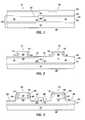
- FIGS. 1-9schematically illustrate, in cross sectional views, a stressed MOS device and methods for its fabrication in accordance with various embodiments of the invention.
- FIGS. 1-9illustrate a stressed MOS device 30 and method steps for manufacturing such an MOS device in accordance with various embodiments of the invention.
- stressed MOS device 30is a CMOS device here illustrated by a single NMOS transistor 31 and a single PMOS transistor 33 .
- the various embodiments of the inventionare particularly directed to the enhancement of the mobility of electrons in the channel of an NMOS transistor.
- an NMOS transistor having enhanced mobilityis fabricated together with a PMOS transistor that also has enhanced mobility to achieve a CMOS device having superior characteristics.
- An integrated circuit formed from stressed MOS devices fabricated in accordance with the inventioncan include a large number of devices such as device 30 , and may also include both stressed and unstressed P-channel MOS transistors and stressed and unstressed N-channel transistors.
- MOS deviceproperly refers to a device having a metal gate electrode and an oxide gate insulator, that term will be used throughout to refer to any semiconductor device that includes a conductive gate electrode (whether metal or other conductive material) that is positioned over a gate insulator (whether oxide or other insulator) which, in turn, is positioned over a semiconductor substrate.
- the fabrication of stressed MOS device 30begins with providing a semiconductor substrate 36 having a surface 32 .
- the semiconductor substratecan be any monocrystalline semiconductor material, but is preferably a monocrystalline silicon substrate wherein the term “silicon substrate” is used herein to encompass the relatively pure silicon materials typically used in the semiconductor industry.
- Semiconductor substrate 36will herein be referred to, for ease of discussion but without limitation, as a silicon substrate.
- semiconductor substrate 36can also be formed of other semiconductor materials such as, for example, silicon germanium (SiGe) comprising between about 10 and about 30 atomic percent germanium in a silicon lattice.
- Silicon substrate 36may be a bulk silicon wafer or a thin layer of silicon 34 on an insulating layer 35 (commonly know as silicon-on-insulator or SOI) that, in turn, is supported by a silicon carrier wafer 37 , but preferably, as here illustrated, without limitation, is an SOI wafer.
- SOIsilicon-on-insulator
- the monocrystalline material forming substrate 36 and specifically thin layer 34 if the substrate is an SOI substratewill be characterized by a lattice constant associated with the crystalline structure of that material.
- portions of thin silicon layer 34will be doped with P-type impurity dopants (a P-well 38 ) for the fabrication of N-channel MOS transistors and other portions will be doped with N-type impurity dopants (an N-well 39 ) for the fabrication of P-channel MOS transistors.
- the P-well and N-wellcan be doped to the appropriate conductivity, for example, by ion implantation.
- Shallow trench isolation (STI) 40 or other form of electrical isolationis formed in the semiconductor substrate and preferably extends through thin layer of silicon 34 to insulating layer 35 to electrically isolate individual devices as required by the circuit function being implemented.
- STIincludes a shallow trench that is etched into the surface of the semiconductor substrate and that is subsequently filled with an insulating material. After the trench is filled with the insulating material the surface is usually planarized, for example by chemical mechanical planarization (CMP).
- CMPchemical mechanical planarization
- the STIgenerally surrounds P-type active areas 42 in P-well 38 and N-type active areas 44 in N-well 39 of silicon substrate 36 .
- a layer of gate insulator 60is formed on the surface of thin silicon layer 34 .
- the gate insulatormay be a thermally grown silicon dioxide formed by heating the silicon substrate in an oxidizing ambient, or may be a deposited insulator such as a silicon oxide, silicon nitride, a high dielectric constant insulator such as HfSiO, or the like. Deposited insulators can be deposited by chemical vapor deposition (CVD), low pressure chemical vapor deposition (LPCVD), or plasma enhanced chemical vapor deposition (PECVD). As illustrated in FIG. 1 , gate insulator 60 is a thermally grown silicon dioxide that grows only at the surface of the silicon layer.
- CVDchemical vapor deposition
- LPCVDlow pressure chemical vapor deposition
- PECVDplasma enhanced chemical vapor deposition
- the gate insulator materialis typically 1-10 nanometers (nm) in thickness. If the semiconductor substrate is a semiconductor material other than silicon, it may be advantageous to deposit the gate insulator. Alternatively, if the substrate is SiGe, it may be advantageous to epitaxially grow a thin stressed silicon layer (not illustrated) on the surface of the SiGe and to thermally oxidize the stressed silicon layer to form a silicon dioxide gate insulator. In accordance with one embodiment of the invention a layer of gate electrode forming material such as polycrystalline silicon 62 is deposited onto the layer of gate insulator. The layer of polycrystalline silicon is preferably deposited as undoped polycrystalline silicon and is subsequently impurity doped by ion implantation.
- the polycrystalline silicon materialcan be deposited, for example, to a thickness of about 100-120 nm by LPCVD by the hydrogen reduction of silane.
- a layer 64 of hard mask materialsuch as silicon oxide, silicon nitride, or silicon oxynitride is deposited onto the surface of the polycrystalline silicon.
- the hard mask materialcan be deposited to a thickness of about 50 nm, also by LPCVD.
- MOS transistor gate electrodes 66 and 68are photolithographically patterned to form MOS transistor gate electrodes 66 and 68 as illustrated in cross section in FIG. 2 .
- Gate electrode 66overlies the portion of P-type active area 42 and P-well 38 of thin silicon layer 34 that will form channel 70 of NMOS transistor 31 at surface 32 .
- gate electrode 68overlies the portion of N-type active area 44 and N-well 39 that will form the channel 72 of PMOS transistor 33 , also at surface 32 .
- the polycrystalline siliconcan be etched in the desired pattern by, for example, plasma etching in a Cl or HBr/O 2 chemistry and the hard mask can be etched, for example, by plasma etching in a CHF 3 , CF 4 , or SF 6 chemistry.
- a thin layer 74 of silicon oxideis thermally grown on the opposing sidewalls 75 and 85 of gate electrode 66 and a thin layer 76 of silicon oxide is thermally grown on the opposing sidewalls 77 and 87 of gate electrode 68 by heating the polycrystalline silicon in an oxidizing ambient.
- Layers 74 and 76can be grown to a thickness of about 2-5 nm.
- Gate electrodes 66 and 68 and layers 74 and 76can be used as an ion implantation mask to form source and drain extensions (not illustrated) on either or both of the MOS transistors.
- layers 74 and 76protect the gate electrode profile.
- the possible need for and method of forming multiple source and drain regionsare well known, but are not germane to this invention and hence need not be explained herein.
- a layer of patterned photoresistcan be used to mask the N-well region during implantation of the source and drain extensions of the PMOS transistor and another layer of patterned photoresist can be used to mask the P-well region during implantation of the source and drain extensions of the NMOS transistor.
- sidewall spacers 80are formed on the thin oxide layer on the opposing sidewalls 75 , 85 and 77 , 87 of gate electrodes 66 and 68 , respectively.
- the sidewall spacerscan be formed of silicon nitride, silicon oxide, or the like by depositing a layer of the spacer material over the gate electrodes and subsequently anisotropically etching the layer, for example by reactive ion etching using a CHF 3 , CF 4 , or SF 6 chemistry.
- Sidewall spacers 80 , gate electrodes 66 and 68 , the hard mask on the top of the gate electrodes, and STI 40are used as an etch mask to etch initial recesses 82 and 84 in the silicon substrate in spaced apart self alignment with the opposing edges of N-channel gate electrode 66 and to etch recesses 86 and 88 in spaced apart self alignment with the opposing edges of P-channel gate electrode 68 .
- the recessesintersect the ends of the channels 70 and 72 .
- the recessescan be anisotropically etched, for example by reactive ion etching using an HBr/O 2 and Cl chemistry.
- each of the recesseshas a depth of about 0.04-0.1 ⁇ m.
- the method in accordance with an embodiment of the inventioncontinues, as illustrated in FIG. 4 , by depositing another layer of spacer forming material 90 .
- a layer of photoresist 92is applied over the layer of spacer forming material and is patterned to leave the layer of photoresist protecting PMOS transistor 33 and exposing NMOS transistor 31 .
- the spacer forming materialcan be silicon nitride, silicon oxide, or the like deposited by, for example, LPCVD.
- the exposed portion of layer of spacer forming material 90is anisotropically etched to form sidewall spacers 94 on the vertical edges of initial recesses 82 and 84 .
- the anisotropic etching of the layer of spacer forming materialexposes the bottoms of initial recesses 82 and 84 while protecting the edges of channel 70 .
- the exposed bottoms of the initial recessesare isotropically etched, for example by plasma etching using an HBr/Cl chemistry together with CF 4 , argon and oxygen to improve the isotropy.
- the isotropic etchingincreases the depth of the initial recesses and also etches sideways under channel 70 .
- the etchingpreferably continues until a recess 96 extends completely under channel 70 .
- semiconductor substrate 36is an SOI substrate
- recess 96preferably extends through the thickness of thin layer of silicon 34 to insulating layer 35 .
- sidewall spacers 94prevent the etching of the semiconductor material forming channel 70 .
- Channel 70thus remains as a bridge of semiconductor material overlying recess 96 and extending from the STI on one side of the active region to the STI on the other side of the active region.
- Recess 96is filled with an expanding material 100 such as silicon nitride, silicon carbide, or other insulators such as zeolite as illustrated in FIG. 7 .
- expanding material 100is thermally grown silicon dioxide. The expanding material fills recess 96 and exerts an upward force on channel 70 as illustrated by arrows 101 .
- the upward force on channel 70applies a uniaxial tensile stress to the channel, and such a tensile stress enhances the mobility of majority carrier electrons in the channel of NMOS transistor 31 .
- Silicon dioxidecan be grown to fill recess 96 , for example, by heating the silicon of channel 70 in an oxidizing ambient. The lower portion of silicon forming channel 70 is oxidized, leaving a layer of silicon overlying the oxide. Silicon dioxide occupies a greater volume than the silicon consumed in the oxidation process.
- an expanding materialsuch as silicon nitride or any other insulator material can be deposited, for example by LPCVD or PECVD, to fill recess 96 .
- Such a deposited materialwould also partially fill recesses 82 and 84 as indicated by the dashed lines 103 .
- the materialexpands and applies the desired upward force on the channel.
- the desired upward forcecan be implemented by a heating cycle to cause the deposited material to at least partially form a lattice structure.
- polycrystalline silicon, polycrystalline silicon germanium, or other conductive or semiconductive material 110is deposited to fill initial recesses 82 and 84 .
- the remainder of spacer forming layer 90protects PMOS transistor 33 .
- the remainder of spacer forming layer 90is removed and a masking layer of silicon oxide or other insulator 112 is deposited and photolithographically patterned to provide a protective masking layer overlying NMOS transistor 31 as illustrated in cross section in FIG. 8 .
- a layer of stress inducing semiconductor material 120 having a lattice constant greater than the lattice constant of the host thin silicon layer 34is selectively epitaxially grown to fill recesses 86 and 88 abutting channel 72 of PMOS transistor 33 .
- the layer of stress inducing semiconductor materialcan be, for example, silicon germanium (SiGe) having about 10-30 atomic percent germanium.
- the SiGehas a greater lattice constant than silicon.
- the layer of stress inducing semiconductor materialcan be any pseudomorphic material that can be epitaxially grown on the semiconductor substrate with a lattice constant greater than the lattice constant of the host semiconductor material.
- the epitaxial growth of layer 120nucleates on the walls and bottom of recesses 86 and 88 . Methods for epitaxially growing SiGe and other stress inducing materials on a silicon or other semiconductor host in a selective manner are will known and need not be described herein. The epitaxial growth is continued until recesses 86 and 88 are filled.
- layer 120During the selective growth of layer 120 , masking layer 112 protects NMOS transistor 31 , so no SiGe deposits on the NMOS transistor. Because SiGe has a greater lattice constant than silicon, layer 120 exerts a compressive longitudinal stress as indicated by arrows 122 on channel 72 of PMOS transistor 33 . Such a compressive longitudinal stress increases the mobility of majority carrier holes in the channel of the PMOS transistor.
- Source and drain regions of the MOS transistorscan be partially or completely in-situ doped with conductivity determining impurities during the process of depositing material 110 and the selective epitaxial growth of layer 120 . Otherwise, following the deposition of material 110 in recesses 82 and 84 , the growth of the stress inducing material 120 in recesses 86 and 88 , and the removal of masking layer 112 , P-type conductivity determining ions are implanted into the stress inducing material in recesses 86 and 88 to form a source region 126 and a drain region 128 of PMOS transistor 33 as illustrated in FIG. 9 .
- N-type conductivity determining ionsare implanted into material 110 in recesses 82 and 84 to form a source region 130 and a drain region 132 of NMOS transistor 31 .
- Appropriate masking, for example with layers of patterned photoresist,can be used in the conventional manner to mask NMOS transistor 31 during the implanting of the P-channel source and drain regions and to mask PMOS transistor 33 during the implanting of the N-channel source and drain regions.
- Stressed MOS device 30can be completed by well known steps (not illustrated) such as depositing a layer of dielectric material, etching opening through the dielectric material to expose portions of the source and drain regions, and forming metallization that extends through the openings to electrically contact the source and drain regions. Further layers of interlayer dielectric material, additional layers of interconnect metallization, and the like may also be applied and patterned to achiever the proper circuit function of the integrated circuit being implemented.
Landscapes
- Insulated Gate Type Field-Effect Transistor (AREA)
- Metal-Oxide And Bipolar Metal-Oxide Semiconductor Integrated Circuits (AREA)
- Thin Film Transistor (AREA)
Abstract
Description
- The present invention generally relates to methods for the fabrication of stressed MOS devices, and more particularly to methods for fabricating stressed NMOS and CMOS devices.
- The majority of present day integrated circuits (ICs) are implemented by using a plurality of interconnected field effect transistors (FETs), also called metal oxide semiconductor field effect transistors (MOSFETs), or simply MOS transistors. An MOS transistor includes a gate electrode as a control electrode and spaced apart source and drain electrodes between which a current can flow. A control voltage applied to the gate electrode controls the flow of current through a channel between the source and drain electrodes.
- MOS transistors, in contrast to bipolar transistor, are majority carrier devices. The gain of an MOS transistor, usually defined by the transconductance (gm), is proportional to the mobility of the majority carrier in the transistor channel. The current carrying capability and hence the performance of an MOS transistor is proportional to the mobility of the majority carrier in the channel. The mobility of holes, the majority carrier in a P-channel MOS (PMOS) transistor can be increased by applying a compressive longitudinal stress to the channel. It is well known that a compressive longitudinal stress can be applied to a silicon MOS transistor by embedding a material such as silicon germanium (SiGe) at the ends of the transistor channel. The mobility of electrons, the majority carrier in an N-channel MOS (NMOS) transistor, however, is decreased by such a compressive longitudinal stress to the channel. To increase the mobility of electrons, a tensile stress must be applied to the channel of the MOS transistor.
- Accordingly, it is desirable to provide a method of fabricating an NMOS transistor having enhanced majority carrier mobility. It is also desirable to provide a method for the fabrication of CMOS devices wherein both the NMOS and PMOS transistors have enhanced majority carrier mobility. Furthermore, other desirable features and characteristics of the present invention will become apparent from the subsequent detailed description and the appended claims, taken in conjunction with the accompanying drawings and the foregoing technical field and background.
- In accordance with one embodiment of the invention a method comprises the steps of providing a monocrystalline semiconductor substrate having a surface and a channel abutting the surface. A gate electrode having a first edge and a second edge is formed overlying the monocrystalline semiconductor substrate. The substrate is anisotropically etched to form a first recess aligned with the first edge and a second recess aligned with the second edge. The substrate is further isotropically etched to form a third recess in the substrate extending beneath the channel. The third recess is filled with an expanding material to exert an upward force on the channel and the first and second recesses are filled with a contact material. Conductivity determining ions are implanted into the contact material to form a source region and a drain region aligned with the first and second edges, respectively.
- The present invention will hereinafter be described in conjunction with the following drawing figures, wherein like numerals denote like elements, and wherein
FIGS. 1-9 schematically illustrate, in cross sectional views, a stressed MOS device and methods for its fabrication in accordance with various embodiments of the invention. - The following detailed description is merely exemplary in nature and is not intended to limit the invention or the application and uses of the invention. Furthermore, there is no intention to be bound by any expressed or implied theory presented in the preceding technical field, background, brief summary or the following detailed description.
FIGS. 1-9 illustrate a stressedMOS device 30 and method steps for manufacturing such an MOS device in accordance with various embodiments of the invention. In this illustrative embodiment stressedMOS device 30 is a CMOS device here illustrated by asingle NMOS transistor 31 and asingle PMOS transistor 33. As will become clear from the following description, the various embodiments of the invention are particularly directed to the enhancement of the mobility of electrons in the channel of an NMOS transistor. In accordance with one embodiment of the invention, however, an NMOS transistor having enhanced mobility is fabricated together with a PMOS transistor that also has enhanced mobility to achieve a CMOS device having superior characteristics. Those of skill in the art will recognize that the invention can be applied to either single channel NMOS devices or to CMOS devices. An integrated circuit formed from stressed MOS devices fabricated in accordance with the invention can include a large number of devices such asdevice 30, and may also include both stressed and unstressed P-channel MOS transistors and stressed and unstressed N-channel transistors.- Various steps in the manufacture of MOS transistors are well known and so, in the interest of brevity, many conventional steps will only be mentioned briefly herein or will be omitted entirely without providing the well known process details. Although the term “MOS device” properly refers to a device having a metal gate electrode and an oxide gate insulator, that term will be used throughout to refer to any semiconductor device that includes a conductive gate electrode (whether metal or other conductive material) that is positioned over a gate insulator (whether oxide or other insulator) which, in turn, is positioned over a semiconductor substrate.
- As illustrated in cross section in
FIG. 1 , the fabrication of stressedMOS device 30, in accordance with an embodiment of the invention, begins with providing asemiconductor substrate 36 having asurface 32. The semiconductor substrate can be any monocrystalline semiconductor material, but is preferably a monocrystalline silicon substrate wherein the term “silicon substrate” is used herein to encompass the relatively pure silicon materials typically used in the semiconductor industry.Semiconductor substrate 36 will herein be referred to, for ease of discussion but without limitation, as a silicon substrate. Those of skill in the art will recognize thatsemiconductor substrate 36 can also be formed of other semiconductor materials such as, for example, silicon germanium (SiGe) comprising between about 10 and about 30 atomic percent germanium in a silicon lattice.Silicon substrate 36 may be a bulk silicon wafer or a thin layer ofsilicon 34 on an insulating layer35 (commonly know as silicon-on-insulator or SOI) that, in turn, is supported by asilicon carrier wafer 37, but preferably, as here illustrated, without limitation, is an SOI wafer. Whether formed of monocrystalline silicon or some other monocrystalline semiconductor material, the monocrystallinematerial forming substrate 36 and specificallythin layer 34 if the substrate is an SOI substrate, will be characterized by a lattice constant associated with the crystalline structure of that material. To fabricate a CMOS device, portions ofthin silicon layer 34 will be doped with P-type impurity dopants (a P-well38) for the fabrication of N-channel MOS transistors and other portions will be doped with N-type impurity dopants (an N-well39) for the fabrication of P-channel MOS transistors. The P-well and N-well can be doped to the appropriate conductivity, for example, by ion implantation. Shallow trench isolation (STI)40 or other form of electrical isolation is formed in the semiconductor substrate and preferably extends through thin layer ofsilicon 34 to insulatinglayer 35 to electrically isolate individual devices as required by the circuit function being implemented. As is well known, there are many processes that can be used to form the STI, so the process need not be described here in detail. In general, STI includes a shallow trench that is etched into the surface of the semiconductor substrate and that is subsequently filled with an insulating material. After the trench is filled with the insulating material the surface is usually planarized, for example by chemical mechanical planarization (CMP). The STI generally surrounds P-typeactive areas 42 in P-well 38 and N-typeactive areas 44 in N-well 39 ofsilicon substrate 36. Although not illustrated, there may be a plurality of N-type active areas and a plurality of P-type active areas, all electrically isolated from each other by the STI, as needed to implement the desired integrated circuit function. - With reference again to
FIG. 1 , a layer ofgate insulator 60 is formed on the surface ofthin silicon layer 34. The gate insulator may be a thermally grown silicon dioxide formed by heating the silicon substrate in an oxidizing ambient, or may be a deposited insulator such as a silicon oxide, silicon nitride, a high dielectric constant insulator such as HfSiO, or the like. Deposited insulators can be deposited by chemical vapor deposition (CVD), low pressure chemical vapor deposition (LPCVD), or plasma enhanced chemical vapor deposition (PECVD). As illustrated inFIG. 1 ,gate insulator 60 is a thermally grown silicon dioxide that grows only at the surface of the silicon layer. The gate insulator material is typically 1-10 nanometers (nm) in thickness. If the semiconductor substrate is a semiconductor material other than silicon, it may be advantageous to deposit the gate insulator. Alternatively, if the substrate is SiGe, it may be advantageous to epitaxially grow a thin stressed silicon layer (not illustrated) on the surface of the SiGe and to thermally oxidize the stressed silicon layer to form a silicon dioxide gate insulator. In accordance with one embodiment of the invention a layer of gate electrode forming material such aspolycrystalline silicon 62 is deposited onto the layer of gate insulator. The layer of polycrystalline silicon is preferably deposited as undoped polycrystalline silicon and is subsequently impurity doped by ion implantation. The polycrystalline silicon material can be deposited, for example, to a thickness of about 100-120 nm by LPCVD by the hydrogen reduction of silane. Alayer 64 of hard mask material such as silicon oxide, silicon nitride, or silicon oxynitride is deposited onto the surface of the polycrystalline silicon. The hard mask material can be deposited to a thickness of about 50 nm, also by LPCVD. - The layer of
polycrystalline silicon 62 and the layer ofhard mask material 64 are photolithographically patterned to form MOStransistor gate electrodes FIG. 2 .Gate electrode 66 overlies the portion of P-typeactive area 42 and P-well 38 ofthin silicon layer 34 that will formchannel 70 ofNMOS transistor 31 atsurface 32. In similarmanner gate electrode 68 overlies the portion of N-typeactive area 44 and N-well 39 that will form thechannel 72 ofPMOS transistor 33, also atsurface 32. The polycrystalline silicon can be etched in the desired pattern by, for example, plasma etching in a Cl or HBr/O2chemistry and the hard mask can be etched, for example, by plasma etching in a CHF3, CF4, or SF6chemistry. Following the patterning of the gate electrode, in accordance with one embodiment of the invention, athin layer 74 of silicon oxide is thermally grown on the opposingsidewalls gate electrode 66 and athin layer 76 of silicon oxide is thermally grown on the opposingsidewalls gate electrode 68 by heating the polycrystalline silicon in an oxidizing ambient.Layers Gate electrodes - In accordance with one embodiment of the invention, as illustrated in
FIG. 3 ,sidewall spacers 80 are formed on the thin oxide layer on the opposingsidewalls gate electrodes Sidewall spacers 80,gate electrodes STI 40 are used as an etch mask to etchinitial recesses channel gate electrode 66 and to etchrecesses channel gate electrode 68. The recesses intersect the ends of thechannels - The method in accordance with an embodiment of the invention continues, as illustrated in
FIG. 4 , by depositing another layer ofspacer forming material 90. A layer of photoresist92 is applied over the layer of spacer forming material and is patterned to leave the layer of photoresist protectingPMOS transistor 33 and exposingNMOS transistor 31. As before, the spacer forming material can be silicon nitride, silicon oxide, or the like deposited by, for example, LPCVD. - As illustrated in
FIG. 5 , the exposed portion of layer ofspacer forming material 90 is anisotropically etched to formsidewall spacers 94 on the vertical edges ofinitial recesses initial recesses channel 70. - As illustrated in
FIG. 6 , the exposed bottoms of the initial recesses are isotropically etched, for example by plasma etching using an HBr/Cl chemistry together with CF4, argon and oxygen to improve the isotropy. The isotropic etching increases the depth of the initial recesses and also etches sideways underchannel 70. The etching preferably continues until arecess 96 extends completely underchannel 70. Ifsemiconductor substrate 36 is an SOI substrate,recess 96 preferably extends through the thickness of thin layer ofsilicon 34 to insulatinglayer 35. During the etching ofrecess 96sidewall spacers 94 prevent the etching of the semiconductormaterial forming channel 70.Channel 70 thus remains as a bridge of semiconductormaterial overlying recess 96 and extending from the STI on one side of the active region to the STI on the other side of the active region. - Following the etching of
recess 96, the method in accordance with one embodiment of the invention continues by removingsidewall spacers 94 and photoresist layer92. As is well known, photoresist layer92 could have also been removed before the etching ofrecess 96. The remainder oflayer 90 continues to maskPMOS transistor 33.Recess 96 is filled with an expandingmaterial 100 such as silicon nitride, silicon carbide, or other insulators such as zeolite as illustrated inFIG. 7 . In accordance with a preferred embodiment, expandingmaterial 100 is thermally grown silicon dioxide. The expanding material fillsrecess 96 and exerts an upward force onchannel 70 as illustrated byarrows 101. The upward force onchannel 70 applies a uniaxial tensile stress to the channel, and such a tensile stress enhances the mobility of majority carrier electrons in the channel ofNMOS transistor 31. Silicon dioxide can be grown to fillrecess 96, for example, by heating the silicon ofchannel 70 in an oxidizing ambient. The lower portion ofsilicon forming channel 70 is oxidized, leaving a layer of silicon overlying the oxide. Silicon dioxide occupies a greater volume than the silicon consumed in the oxidation process. Alternatively, an expanding material such as silicon nitride or any other insulator material can be deposited, for example by LPCVD or PECVD, to fillrecess 96. Such a deposited material would also partially fillrecesses lines 103. In the case of a high temperature deposition, as the material cools following deposition, the material expands and applies the desired upward force on the channel. Alternatively, for those materials that are deposited at a low temperature, the desired upward force can be implemented by a heating cycle to cause the deposited material to at least partially form a lattice structure. Following the deposition of the expanding material, polycrystalline silicon, polycrystalline silicon germanium, or other conductive orsemiconductive material 110 is deposited to fillinitial recesses NMOS transistor 31, the remainder ofspacer forming layer 90 protectsPMOS transistor 33. - In accordance with one embodiment of the invention, after depositing
material 110, the remainder ofspacer forming layer 90 is removed and a masking layer of silicon oxide orother insulator 112 is deposited and photolithographically patterned to provide a protective masking layer overlyingNMOS transistor 31 as illustrated in cross section inFIG. 8 . A layer of stress inducingsemiconductor material 120 having a lattice constant greater than the lattice constant of the hostthin silicon layer 34 is selectively epitaxially grown to fillrecesses channel 72 ofPMOS transistor 33. For a host silicon material, the layer of stress inducing semiconductor material can be, for example, silicon germanium (SiGe) having about 10-30 atomic percent germanium. The SiGe has a greater lattice constant than silicon. In general, the layer of stress inducing semiconductor material can be any pseudomorphic material that can be epitaxially grown on the semiconductor substrate with a lattice constant greater than the lattice constant of the host semiconductor material. The epitaxial growth oflayer 120 nucleates on the walls and bottom ofrecesses recesses layer 120, maskinglayer 112 protectsNMOS transistor 31, so no SiGe deposits on the NMOS transistor. Because SiGe has a greater lattice constant than silicon,layer 120 exerts a compressive longitudinal stress as indicated byarrows 122 onchannel 72 ofPMOS transistor 33. Such a compressive longitudinal stress increases the mobility of majority carrier holes in the channel of the PMOS transistor. - Source and drain regions of the MOS transistors can be partially or completely in-situ doped with conductivity determining impurities during the process of depositing
material 110 and the selective epitaxial growth oflayer 120. Otherwise, following the deposition ofmaterial 110 inrecesses stress inducing material 120 inrecesses masking layer 112, P-type conductivity determining ions are implanted into the stress inducing material inrecesses source region 126 and adrain region 128 ofPMOS transistor 33 as illustrated inFIG. 9 . Similarly, N-type conductivity determining ions are implanted intomaterial 110 inrecesses source region 130 and adrain region 132 ofNMOS transistor 31. Appropriate masking, for example with layers of patterned photoresist, can be used in the conventional manner to maskNMOS transistor 31 during the implanting of the P-channel source and drain regions and to maskPMOS transistor 33 during the implanting of the N-channel source and drain regions. Stressed MOS device 30 can be completed by well known steps (not illustrated) such as depositing a layer of dielectric material, etching opening through the dielectric material to expose portions of the source and drain regions, and forming metallization that extends through the openings to electrically contact the source and drain regions. Further layers of interlayer dielectric material, additional layers of interconnect metallization, and the like may also be applied and patterned to achiever the proper circuit function of the integrated circuit being implemented.- While at least one exemplary embodiment has been presented in the foregoing detailed description, it should be appreciated that a vast number of variations exist. It should also be appreciated that the exemplary embodiment or exemplary embodiments are only examples, and are not intended to limit the scope, applicability, or configuration of the invention in any way. Rather, the foregoing detailed description will provide those skilled in the art with a convenient road map for implementing the exemplary embodiment or exemplary embodiments. It should be understood that various changes can be made in the function and arrangement of elements without departing from the scope of the invention as set forth in the appended claims and the legal equivalents thereof.
Claims (20)
Priority Applications (3)
| Application Number | Priority Date | Filing Date | Title |
|---|---|---|---|
| US11/235,791US7326601B2 (en) | 2005-09-26 | 2005-09-26 | Methods for fabrication of a stressed MOS device |
| PCT/US2006/032755WO2007037847A1 (en) | 2005-09-26 | 2006-08-23 | Methods for fabrication of a stressed mos device |
| TW095133589ATWI483315B (en) | 2005-09-26 | 2006-09-12 | Method for manufacturing a stressed MOS device |
Applications Claiming Priority (1)
| Application Number | Priority Date | Filing Date | Title |
|---|---|---|---|
| US11/235,791US7326601B2 (en) | 2005-09-26 | 2005-09-26 | Methods for fabrication of a stressed MOS device |
Publications (2)
| Publication Number | Publication Date |
|---|---|
| US20070072380A1true US20070072380A1 (en) | 2007-03-29 |
| US7326601B2 US7326601B2 (en) | 2008-02-05 |
Family
ID=37496665
Family Applications (1)
| Application Number | Title | Priority Date | Filing Date |
|---|---|---|---|
| US11/235,791Expired - Fee RelatedUS7326601B2 (en) | 2005-09-26 | 2005-09-26 | Methods for fabrication of a stressed MOS device |
Country Status (3)
| Country | Link |
|---|---|
| US (1) | US7326601B2 (en) |
| TW (1) | TWI483315B (en) |
| WO (1) | WO2007037847A1 (en) |
Cited By (15)
| Publication number | Priority date | Publication date | Assignee | Title |
|---|---|---|---|---|
| US20050176219A1 (en)* | 2004-02-06 | 2005-08-11 | Min-Sang Kim | Methods of forming MOSFETs using crystalline sacrificial structures and MOSFETs so formed |
| US20070176235A1 (en)* | 2006-01-27 | 2007-08-02 | Renesas Technology Corp. | Semiconductor device and manufacturing method for the same |
| US20070241414A1 (en)* | 2004-06-10 | 2007-10-18 | Mitsuru Narihiro | Semiconductor Device and Manufacturing Process Therefor |
| US20080099859A1 (en)* | 2006-11-01 | 2008-05-01 | Nec Electronics Corporation | Method of manufacturing semiconductor device having of spacer gate structure |
| US7410859B1 (en)* | 2005-11-07 | 2008-08-12 | Advanced Micro Devices, Inc. | Stressed MOS device and method for its fabrication |
| FR2920252A1 (en)* | 2007-08-24 | 2009-02-27 | Commissariat Energie Atomique | Transistor e.g. MOSFET, forming method, involves forming catalyst layer, extending nanometric linear conductors from catalyst layer, and depositing encapsulation layer that covers transistor and linear conductors |
| US20090072312A1 (en)* | 2007-09-14 | 2009-03-19 | Leland Chang | Metal High-K (MHK) Dual Gate Stress Engineering Using Hybrid Orientation (HOT) CMOS |
| US20100219474A1 (en)* | 2009-02-27 | 2010-09-02 | Stephan Kronholz | Transistor comprising an embedded semiconductor alloy in drain and source regions extending under the gate electrode |
| US20120306027A1 (en)* | 2011-05-30 | 2012-12-06 | Globalfoundries Inc. | Transistors with embedded strain-inducing material formed in cavities provided by an oxidizing etch process |
| US20130210207A1 (en)* | 2009-11-30 | 2013-08-15 | Fujitsu Semiconductor Limited | Fabrication method of semiconductor device and fabrication method of dynamic threshold transistor |
| US20140239401A1 (en)* | 2013-02-25 | 2014-08-28 | International Business Machines Corporation | Silicon nitride gate encapsulation by implantation |
| CN105895532A (en)* | 2016-06-14 | 2016-08-24 | 西安电子科技大学 | N-channel metal oxide semiconductor (NMOS) device based on [110] single-shaft tensile stress of [100]/(001) channel and fabrication method of NMOS device |
| US20170229480A1 (en)* | 2016-02-05 | 2017-08-10 | Taiwan Semiconductor Manufacturing Company Limited | Semiconductor device including a high-electron-mobility transistor (hemt) and method for manufacturing the same |
| US9741853B2 (en)* | 2015-10-29 | 2017-08-22 | Globalfoundries Inc. | Stress memorization techniques for transistor devices |
| US20220352373A1 (en)* | 2006-12-11 | 2022-11-03 | Sony Group Corporation | Metal oxide semiconductor having epitaxial source drain regions and a method of manufacturing same using dummy gate process |
Families Citing this family (7)
| Publication number | Priority date | Publication date | Assignee | Title |
|---|---|---|---|---|
| FR2872626B1 (en)* | 2004-07-05 | 2008-05-02 | Commissariat Energie Atomique | METHOD FOR CONTRAINDING A THIN PATTERN |
| US20060226492A1 (en)* | 2005-03-30 | 2006-10-12 | Bich-Yen Nguyen | Semiconductor device featuring an arched structure strained semiconductor layer |
| DE102006015090B4 (en)* | 2006-03-31 | 2008-03-13 | Advanced Micro Devices, Inc., Sunnyvale | Method for producing different embedded deformation layers in transistors |
| DE102009010847B4 (en)* | 2009-02-27 | 2012-12-27 | Advanced Micro Devices, Inc. | Integrate semiconductor alloys into PMOS and NMOS transistors using a common recess etch process |
| US8461005B2 (en)* | 2010-03-03 | 2013-06-11 | United Microelectronics Corp. | Method of manufacturing doping patterns |
| CN102237396B (en)* | 2010-04-27 | 2014-04-09 | 中国科学院微电子研究所 | Semiconductor device and method for manufacturing the same |
| CN103165448B (en)* | 2011-12-08 | 2016-01-06 | 中芯国际集成电路制造(上海)有限公司 | The formation method of PMOS transistor |
Citations (13)
| Publication number | Priority date | Publication date | Assignee | Title |
|---|---|---|---|---|
| US477411A (en)* | 1892-06-21 | Dental plugger | ||
| US2098495A (en)* | 1934-02-10 | 1937-11-09 | Ind Hammer Dev Corp | Mechanical mallet |
| US4382827A (en)* | 1981-04-27 | 1983-05-10 | Ncr Corporation | Silicon nitride S/D ion implant mask in CMOS device fabrication |
| US5094617A (en)* | 1990-12-11 | 1992-03-10 | Carr Gary B | Dental retro-filling preparation tool and method |
| US5106306A (en)* | 1991-01-29 | 1992-04-21 | Telephone Products, Inc. | Rotary electrical connector with remote modular connector |
| US6165826A (en)* | 1994-12-23 | 2000-12-26 | Intel Corporation | Transistor with low resistance tip and method of fabrication in a CMOS process |
| US6204145B1 (en)* | 1996-11-12 | 2001-03-20 | Micron Technology, Inc. | Silicon-on-insulator islands and method for their formation |
| US6382965B1 (en)* | 2000-04-25 | 2002-05-07 | Ormco Corporation | Orthodontic debonding tools and methods |
| US20020086472A1 (en)* | 2000-12-29 | 2002-07-04 | Brian Roberds | Technique to obtain high mobility channels in MOS transistors by forming a strain layer on an underside of a channel |
| US20040108559A1 (en)* | 2002-10-02 | 2004-06-10 | Renesas Technology Corp. | Insulated-gate field-effect transistor, method of fabricating same, and semiconductor device employing same |
| US20040217391A1 (en)* | 2003-04-29 | 2004-11-04 | Micron Technology, Inc. | Localized strained semiconductor on insulator |
| US20050064669A1 (en)* | 2003-09-23 | 2005-03-24 | Orlowski Marius K. | Method for forming a semiconductor device having isolation regions |
| US6989570B2 (en)* | 2002-04-03 | 2006-01-24 | Stmicroelectronics S.A. | Strained-channel isolated-gate field effect transistor, process for making same and resulting integrated circuit |
Family Cites Families (2)
| Publication number | Priority date | Publication date | Assignee | Title |
|---|---|---|---|---|
| JP3678661B2 (en)* | 2001-03-08 | 2005-08-03 | シャープ株式会社 | Semiconductor device |
| JP2004228273A (en)* | 2003-01-22 | 2004-08-12 | Renesas Technology Corp | Semiconductor device |
- 2005
- 2005-09-26USUS11/235,791patent/US7326601B2/ennot_activeExpired - Fee Related
- 2006
- 2006-08-23WOPCT/US2006/032755patent/WO2007037847A1/enactiveApplication Filing
- 2006-09-12TWTW095133589Apatent/TWI483315B/ennot_activeIP Right Cessation
Patent Citations (14)
| Publication number | Priority date | Publication date | Assignee | Title |
|---|---|---|---|---|
| US477411A (en)* | 1892-06-21 | Dental plugger | ||
| US2098495A (en)* | 1934-02-10 | 1937-11-09 | Ind Hammer Dev Corp | Mechanical mallet |
| US4382827A (en)* | 1981-04-27 | 1983-05-10 | Ncr Corporation | Silicon nitride S/D ion implant mask in CMOS device fabrication |
| US5094617A (en)* | 1990-12-11 | 1992-03-10 | Carr Gary B | Dental retro-filling preparation tool and method |
| US5094617B1 (en)* | 1990-12-11 | 1997-03-11 | Gary B Carr | Dental retro-filling preparation tool and method |
| US5106306A (en)* | 1991-01-29 | 1992-04-21 | Telephone Products, Inc. | Rotary electrical connector with remote modular connector |
| US6165826A (en)* | 1994-12-23 | 2000-12-26 | Intel Corporation | Transistor with low resistance tip and method of fabrication in a CMOS process |
| US6204145B1 (en)* | 1996-11-12 | 2001-03-20 | Micron Technology, Inc. | Silicon-on-insulator islands and method for their formation |
| US6382965B1 (en)* | 2000-04-25 | 2002-05-07 | Ormco Corporation | Orthodontic debonding tools and methods |
| US20020086472A1 (en)* | 2000-12-29 | 2002-07-04 | Brian Roberds | Technique to obtain high mobility channels in MOS transistors by forming a strain layer on an underside of a channel |
| US6989570B2 (en)* | 2002-04-03 | 2006-01-24 | Stmicroelectronics S.A. | Strained-channel isolated-gate field effect transistor, process for making same and resulting integrated circuit |
| US20040108559A1 (en)* | 2002-10-02 | 2004-06-10 | Renesas Technology Corp. | Insulated-gate field-effect transistor, method of fabricating same, and semiconductor device employing same |
| US20040217391A1 (en)* | 2003-04-29 | 2004-11-04 | Micron Technology, Inc. | Localized strained semiconductor on insulator |
| US20050064669A1 (en)* | 2003-09-23 | 2005-03-24 | Orlowski Marius K. | Method for forming a semiconductor device having isolation regions |
Cited By (33)
| Publication number | Priority date | Publication date | Assignee | Title |
|---|---|---|---|---|
| US20100012990A1 (en)* | 2004-02-06 | 2010-01-21 | Min-Sang Kim | Mosfets including crystalline sacrificial structures |
| US20050176219A1 (en)* | 2004-02-06 | 2005-08-11 | Min-Sang Kim | Methods of forming MOSFETs using crystalline sacrificial structures and MOSFETs so formed |
| US7605025B2 (en)* | 2004-02-06 | 2009-10-20 | Samsung Electronics Co., Ltd. | Methods of forming MOSFETS using crystalline sacrificial structures |
| US8486811B2 (en) | 2004-06-10 | 2013-07-16 | Nec Corporation | Semiconductor device and manufacturing process therefor |
| US20070241414A1 (en)* | 2004-06-10 | 2007-10-18 | Mitsuru Narihiro | Semiconductor Device and Manufacturing Process Therefor |
| US7989855B2 (en)* | 2004-06-10 | 2011-08-02 | Nec Corporation | Semiconductor device including a deflected part |
| US7410859B1 (en)* | 2005-11-07 | 2008-08-12 | Advanced Micro Devices, Inc. | Stressed MOS device and method for its fabrication |
| US20080258175A1 (en)* | 2005-11-07 | 2008-10-23 | Advanced Micro Devices, Inc. | Stressed mos device |
| US7696534B2 (en) | 2005-11-07 | 2010-04-13 | Advanced Micro Devices, Inc. | Stressed MOS device |
| US8350331B2 (en)* | 2006-01-27 | 2013-01-08 | Renesas Electronics Corporation | Semiconductor device and manufacturing method for the same |
| US20070176235A1 (en)* | 2006-01-27 | 2007-08-02 | Renesas Technology Corp. | Semiconductor device and manufacturing method for the same |
| US20080099859A1 (en)* | 2006-11-01 | 2008-05-01 | Nec Electronics Corporation | Method of manufacturing semiconductor device having of spacer gate structure |
| US7935592B2 (en)* | 2006-11-01 | 2011-05-03 | Renesas Electronics Corporation | Method of manufacturing semiconductor device having of spacer gate structure |
| US11901454B2 (en)* | 2006-12-11 | 2024-02-13 | Sony Group Corporation | Metal oxide semiconductor having epitaxial source drain regions and a method of manufacturing same using dummy gate process |
| US20220352373A1 (en)* | 2006-12-11 | 2022-11-03 | Sony Group Corporation | Metal oxide semiconductor having epitaxial source drain regions and a method of manufacturing same using dummy gate process |
| FR2920252A1 (en)* | 2007-08-24 | 2009-02-27 | Commissariat Energie Atomique | Transistor e.g. MOSFET, forming method, involves forming catalyst layer, extending nanometric linear conductors from catalyst layer, and depositing encapsulation layer that covers transistor and linear conductors |
| US20100159684A1 (en)* | 2007-09-14 | 2010-06-24 | International Business Machines Corporation | Metal High-K (MHK) Dual Gate Stress Engineering Using Hybrid Orientation (HOT) CMOS |
| US20090072312A1 (en)* | 2007-09-14 | 2009-03-19 | Leland Chang | Metal High-K (MHK) Dual Gate Stress Engineering Using Hybrid Orientation (HOT) CMOS |
| US20100219474A1 (en)* | 2009-02-27 | 2010-09-02 | Stephan Kronholz | Transistor comprising an embedded semiconductor alloy in drain and source regions extending under the gate electrode |
| US8460980B2 (en)* | 2009-02-27 | 2013-06-11 | Globalfoundries Inc. | Transistor comprising an embedded semiconductor alloy in drain and source regions extending under the gate electrode |
| US9178034B2 (en) | 2009-11-30 | 2015-11-03 | Fujitsu Semiconductor Limited | Fabrication method of semiconductor device and fabrication method of dynamic threshold transistor |
| US20130210207A1 (en)* | 2009-11-30 | 2013-08-15 | Fujitsu Semiconductor Limited | Fabrication method of semiconductor device and fabrication method of dynamic threshold transistor |
| US8709898B2 (en)* | 2009-11-30 | 2014-04-29 | Fujitsu Semiconductor Limited | Fabrication method of semiconductor device and fabrication method of dynamic threshold transistor |
| US8674458B2 (en)* | 2011-05-30 | 2014-03-18 | Globalfoundries Inc. | Transistors with embedded strain-inducing material formed in cavities provided by an oxidizing etch process |
| US20120306027A1 (en)* | 2011-05-30 | 2012-12-06 | Globalfoundries Inc. | Transistors with embedded strain-inducing material formed in cavities provided by an oxidizing etch process |
| US8906759B2 (en)* | 2013-02-25 | 2014-12-09 | International Business Machines Corporation | Silicon nitride gate encapsulation by implantation |
| US8912612B2 (en)* | 2013-02-25 | 2014-12-16 | International Business Machines Corporation | Silicon nitride gate encapsulation by implantation |
| US20140239420A1 (en)* | 2013-02-25 | 2014-08-28 | International Business Machines Corporation | Silicon nitride gate encapsulation by implantation |
| US20140239401A1 (en)* | 2013-02-25 | 2014-08-28 | International Business Machines Corporation | Silicon nitride gate encapsulation by implantation |
| US9741853B2 (en)* | 2015-10-29 | 2017-08-22 | Globalfoundries Inc. | Stress memorization techniques for transistor devices |
| US20170229480A1 (en)* | 2016-02-05 | 2017-08-10 | Taiwan Semiconductor Manufacturing Company Limited | Semiconductor device including a high-electron-mobility transistor (hemt) and method for manufacturing the same |
| US10153300B2 (en)* | 2016-02-05 | 2018-12-11 | Taiwan Semiconductor Manufacturing Company Limited | Semiconductor device including a high-electron-mobility transistor (HEMT) and method for manufacturing the same |
| CN105895532A (en)* | 2016-06-14 | 2016-08-24 | 西安电子科技大学 | N-channel metal oxide semiconductor (NMOS) device based on [110] single-shaft tensile stress of [100]/(001) channel and fabrication method of NMOS device |
Also Published As
| Publication number | Publication date |
|---|---|
| WO2007037847A1 (en) | 2007-04-05 |
| US7326601B2 (en) | 2008-02-05 |
| TW200739745A (en) | 2007-10-16 |
| TWI483315B (en) | 2015-05-01 |
Similar Documents
| Publication | Publication Date | Title |
|---|---|---|
| US7696534B2 (en) | Stressed MOS device | |
| US7326601B2 (en) | Methods for fabrication of a stressed MOS device | |
| CN101233605B (en) | Methods for fabricating a stressed MOS device | |
| US8159030B2 (en) | Strained MOS device and methods for its fabrication | |
| US8148214B2 (en) | Stressed field effect transistor and methods for its fabrication | |
| US7741164B2 (en) | Method for fabricating SOI device | |
| TWI440097B (en) | Stress-enhanced MOS transistor and method of manufacturing same | |
| US7902008B2 (en) | Methods for fabricating a stressed MOS device | |
| US8828839B2 (en) | Methods for fabricating electrically-isolated finFET semiconductor devices | |
| US7601574B2 (en) | Methods for fabricating a stress enhanced MOS transistor | |
| US7893496B2 (en) | Stress enhanced transistor | |
| US7439120B2 (en) | Method for fabricating stress enhanced MOS circuits | |
| US20090289280A1 (en) | Method for Making Transistors and the Device Thereof | |
| US20100207175A1 (en) | Semiconductor transistor device having an asymmetric embedded stressor configuration, and related manufacturing method | |
| US7977180B2 (en) | Methods for fabricating stressed MOS devices | |
| US20090050963A1 (en) | Stressed mos device and methods for its fabrication | |
| US7462524B1 (en) | Methods for fabricating a stressed MOS device |
Legal Events
| Date | Code | Title | Description |
|---|---|---|---|
| AS | Assignment | Owner name:ADVANCED MICRO DEVICES, INC., CALIFORNIA Free format text:ASSIGNMENT OF ASSIGNORS INTEREST;ASSIGNORS:WIRBELEIT, FRANK;BLACK, LINDA R.;PEIDOUS, IGOR;REEL/FRAME:017041/0051;SIGNING DATES FROM 20050914 TO 20050922 | |
| FEPP | Fee payment procedure | Free format text:PAYOR NUMBER ASSIGNED (ORIGINAL EVENT CODE: ASPN); ENTITY STATUS OF PATENT OWNER: LARGE ENTITY | |
| STCF | Information on status: patent grant | Free format text:PATENTED CASE | |
| AS | Assignment | Owner name:GLOBALFOUNDRIES INC., CAYMAN ISLANDS Free format text:AFFIRMATION OF PATENT ASSIGNMENT;ASSIGNOR:ADVANCED MICRO DEVICES, INC.;REEL/FRAME:023119/0083 Effective date:20090630 | |
| FPAY | Fee payment | Year of fee payment:4 | |
| FPAY | Fee payment | Year of fee payment:8 | |
| AS | Assignment | Owner name:ALSEPHINA INNOVATIONS INC., CANADA Free format text:ASSIGNMENT OF ASSIGNORS INTEREST;ASSIGNOR:GLOBALFOUNDRIES INC.;REEL/FRAME:049709/0871 Effective date:20181126 | |
| FEPP | Fee payment procedure | Free format text:MAINTENANCE FEE REMINDER MAILED (ORIGINAL EVENT CODE: REM.); ENTITY STATUS OF PATENT OWNER: LARGE ENTITY | |
| LAPS | Lapse for failure to pay maintenance fees | Free format text:PATENT EXPIRED FOR FAILURE TO PAY MAINTENANCE FEES (ORIGINAL EVENT CODE: EXP.); ENTITY STATUS OF PATENT OWNER: LARGE ENTITY | |
| STCH | Information on status: patent discontinuation | Free format text:PATENT EXPIRED DUE TO NONPAYMENT OF MAINTENANCE FEES UNDER 37 CFR 1.362 | |
| FP | Lapsed due to failure to pay maintenance fee | Effective date:20200205 | |
| AS | Assignment | Owner name:TAIWAN SEMICONDUCTOR MANUFACTURING COMPANY, LTD., TAIWAN Free format text:ASSIGNMENT OF ASSIGNORS INTEREST;ASSIGNOR:ALSEPHINA INNOVATIONS, INC.;REEL/FRAME:053351/0839 Effective date:20200211 | |
| AS | Assignment | Owner name:GLOBALFOUNDRIES INC., CAYMAN ISLANDS Free format text:RELEASE BY SECURED PARTY;ASSIGNOR:WILMINGTON TRUST, NATIONAL ASSOCIATION;REEL/FRAME:054636/0001 Effective date:20201117 |