US20070072354A1 - Structures with planar strained layers - Google Patents
Structures with planar strained layersDownload PDFInfo
- Publication number
- US20070072354A1 US20070072354A1US11/584,181US58418106AUS2007072354A1US 20070072354 A1US20070072354 A1US 20070072354A1US 58418106 AUS58418106 AUS 58418106AUS 2007072354 A1US2007072354 A1US 2007072354A1
- Authority
- US
- United States
- Prior art keywords
- layer
- strained
- semiconductor
- compressively strained
- gate
- Prior art date
- Legal status (The legal status is an assumption and is not a legal conclusion. Google has not performed a legal analysis and makes no representation as to the accuracy of the status listed.)
- Abandoned
Links
- 239000004065semiconductorSubstances0.000claimsabstractdescription44
- 238000000034methodMethods0.000claimsabstractdescription26
- 229910052710siliconInorganic materials0.000claimsdescription30
- XUIMIQQOPSSXEZ-UHFFFAOYSA-NSiliconChemical compound[Si]XUIMIQQOPSSXEZ-UHFFFAOYSA-N0.000claimsdescription27
- 239000010703siliconSubstances0.000claimsdescription25
- 229910052732germaniumInorganic materials0.000claimsdescription16
- 239000000758substrateSubstances0.000claimsdescription15
- 230000005669field effectEffects0.000claimsdescription14
- 239000002019doping agentSubstances0.000claimsdescription12
- GNPVGFCGXDBREM-UHFFFAOYSA-Ngermanium atomChemical compound[Ge]GNPVGFCGXDBREM-UHFFFAOYSA-N0.000claimsdescription10
- 229910000577Silicon-germaniumInorganic materials0.000claimsdescription9
- 230000000295complement effectEffects0.000claimsdescription2
- 230000003746surface roughnessEffects0.000abstractdescription9
- 238000000151depositionMethods0.000description19
- 230000008021depositionEffects0.000description18
- 230000015572biosynthetic processEffects0.000description10
- 239000007789gasSubstances0.000description8
- 230000037230mobilityEffects0.000description8
- 238000000038ultrahigh vacuum chemical vapour depositionMethods0.000description8
- 238000005229chemical vapour depositionMethods0.000description7
- 125000004429atomChemical group0.000description6
- VYPSYNLAJGMNEJ-UHFFFAOYSA-NSilicium dioxideChemical compoundO=[Si]=OVYPSYNLAJGMNEJ-UHFFFAOYSA-N0.000description4
- QUZPNFFHZPRKJD-UHFFFAOYSA-NgermaneChemical compound[GeH4]QUZPNFFHZPRKJD-UHFFFAOYSA-N0.000description4
- 229910052986germanium hydrideInorganic materials0.000description4
- PFNQVRZLDWYSCW-UHFFFAOYSA-N(fluoren-9-ylideneamino) n-naphthalen-1-ylcarbamateChemical compoundC12=CC=CC=C2C2=CC=CC=C2C1=NOC(=O)NC1=CC=CC2=CC=CC=C12PFNQVRZLDWYSCW-UHFFFAOYSA-N0.000description3
- MARUHZGHZWCEQU-UHFFFAOYSA-N5-phenyl-2h-tetrazoleChemical compoundC1=CC=CC=C1C1=NNN=N1MARUHZGHZWCEQU-UHFFFAOYSA-N0.000description3
- JBRZTFJDHDCESZ-UHFFFAOYSA-NAsGaChemical compound[As]#[Ga]JBRZTFJDHDCESZ-UHFFFAOYSA-N0.000description3
- 229910005540GaPInorganic materials0.000description3
- 229910001218Gallium arsenideInorganic materials0.000description3
- 229910000530Gallium indium arsenideInorganic materials0.000description3
- 229910006990Si1-xGexInorganic materials0.000description3
- 229910007020Si1−xGexInorganic materials0.000description3
- NINIDFKCEFEMDL-UHFFFAOYSA-NSulfurChemical compound[S]NINIDFKCEFEMDL-UHFFFAOYSA-N0.000description3
- 239000005864SulphurSubstances0.000description3
- KXNLCSXBJCPWGL-UHFFFAOYSA-N[Ga].[As].[In]Chemical compound[Ga].[As].[In]KXNLCSXBJCPWGL-UHFFFAOYSA-N0.000description3
- HZXMRANICFIONG-UHFFFAOYSA-Ngallium phosphideChemical compound[Ga]#PHZXMRANICFIONG-UHFFFAOYSA-N0.000description3
- 229910021480group 4 elementInorganic materials0.000description3
- 229910021478group 5 elementInorganic materials0.000description3
- 229910021476group 6 elementInorganic materials0.000description3
- 229910052738indiumInorganic materials0.000description3
- APFVFJFRJDLVQX-UHFFFAOYSA-Nindium atomChemical compound[In]APFVFJFRJDLVQX-UHFFFAOYSA-N0.000description3
- VCEXCCILEWFFBG-UHFFFAOYSA-Nmercury tellurideChemical compound[Hg]=[Te]VCEXCCILEWFFBG-UHFFFAOYSA-N0.000description3
- UFHFLCQGNIYNRP-UHFFFAOYSA-NHydrogenChemical compound[H][H]UFHFLCQGNIYNRP-UHFFFAOYSA-N0.000description2
- OAICVXFJPJFONN-UHFFFAOYSA-NPhosphorusChemical compound[P]OAICVXFJPJFONN-UHFFFAOYSA-N0.000description2
- BLRPTPMANUNPDV-UHFFFAOYSA-NSilaneChemical compound[SiH4]BLRPTPMANUNPDV-UHFFFAOYSA-N0.000description2
- 230000004913activationEffects0.000description2
- 229910052785arsenicInorganic materials0.000description2
- RQNWIZPPADIBDY-UHFFFAOYSA-Narsenic atomChemical compound[As]RQNWIZPPADIBDY-UHFFFAOYSA-N0.000description2
- 238000001505atmospheric-pressure chemical vapour depositionMethods0.000description2
- 238000000354decomposition reactionMethods0.000description2
- 229910000078germaneInorganic materials0.000description2
- 229910052739hydrogenInorganic materials0.000description2
- 239000001257hydrogenSubstances0.000description2
- 125000004435hydrogen atomChemical group[H]*0.000description2
- 238000004518low pressure chemical vapour depositionMethods0.000description2
- 230000005012migrationEffects0.000description2
- 238000013508migrationMethods0.000description2
- 229910052698phosphorusInorganic materials0.000description2
- 239000011574phosphorusSubstances0.000description2
- 229910021420polycrystalline siliconInorganic materials0.000description2
- 229920005591polysiliconPolymers0.000description2
- 230000008569processEffects0.000description2
- 229910000077silaneInorganic materials0.000description2
- 235000012239silicon dioxideNutrition0.000description2
- 239000000377silicon dioxideSubstances0.000description2
- ZOXJGFHDIHLPTG-UHFFFAOYSA-NBoronChemical compound[B]ZOXJGFHDIHLPTG-UHFFFAOYSA-N0.000description1
- LEVVHYCKPQWKOP-UHFFFAOYSA-N[Si].[Ge]Chemical compound[Si].[Ge]LEVVHYCKPQWKOP-UHFFFAOYSA-N0.000description1
- 230000009286beneficial effectEffects0.000description1
- 230000008901benefitEffects0.000description1
- 229910052796boronInorganic materials0.000description1
- 239000000969carrierSubstances0.000description1
- 238000005137deposition processMethods0.000description1
- 238000013461designMethods0.000description1
- 238000011161developmentMethods0.000description1
- 239000012535impuritySubstances0.000description1
- 238000010348incorporationMethods0.000description1
- 238000004519manufacturing processMethods0.000description1
- 239000000463materialSubstances0.000description1
- 230000007246mechanismEffects0.000description1
- 238000002161passivationMethods0.000description1
- 230000000135prohibitive effectEffects0.000description1
- 230000009467reductionEffects0.000description1
- 238000005204segregationMethods0.000description1
- 230000007704transitionEffects0.000description1
Images


Classifications
- H—ELECTRICITY
- H10—SEMICONDUCTOR DEVICES; ELECTRIC SOLID-STATE DEVICES NOT OTHERWISE PROVIDED FOR
- H10D—INORGANIC ELECTRIC SEMICONDUCTOR DEVICES
- H10D30/00—Field-effect transistors [FET]
- H10D30/60—Insulated-gate field-effect transistors [IGFET]
- H10D30/751—Insulated-gate field-effect transistors [IGFET] having composition variations in the channel regions
- H—ELECTRICITY
- H10—SEMICONDUCTOR DEVICES; ELECTRIC SOLID-STATE DEVICES NOT OTHERWISE PROVIDED FOR
- H10D—INORGANIC ELECTRIC SEMICONDUCTOR DEVICES
- H10D30/00—Field-effect transistors [FET]
- H10D30/60—Insulated-gate field-effect transistors [IGFET]
- H—ELECTRICITY
- H10—SEMICONDUCTOR DEVICES; ELECTRIC SOLID-STATE DEVICES NOT OTHERWISE PROVIDED FOR
- H10D—INORGANIC ELECTRIC SEMICONDUCTOR DEVICES
- H10D30/00—Field-effect transistors [FET]
- H10D30/80—FETs having rectifying junction gate electrodes
- H10D30/801—FETs having heterojunction gate electrodes
- H—ELECTRICITY
- H10—SEMICONDUCTOR DEVICES; ELECTRIC SOLID-STATE DEVICES NOT OTHERWISE PROVIDED FOR
- H10D—INORGANIC ELECTRIC SEMICONDUCTOR DEVICES
- H10D84/00—Integrated devices formed in or on semiconductor substrates that comprise only semiconducting layers, e.g. on Si wafers or on GaAs-on-Si wafers
- H10D84/01—Manufacture or treatment
- H10D84/0123—Integrating together multiple components covered by H10D12/00 or H10D30/00, e.g. integrating multiple IGBTs
- H10D84/0126—Integrating together multiple components covered by H10D12/00 or H10D30/00, e.g. integrating multiple IGBTs the components including insulated gates, e.g. IGFETs
- H10D84/0165—Integrating together multiple components covered by H10D12/00 or H10D30/00, e.g. integrating multiple IGBTs the components including insulated gates, e.g. IGFETs the components including complementary IGFETs, e.g. CMOS devices
- H10D84/0167—Manufacturing their channels
- H—ELECTRICITY
- H10—SEMICONDUCTOR DEVICES; ELECTRIC SOLID-STATE DEVICES NOT OTHERWISE PROVIDED FOR
- H10D—INORGANIC ELECTRIC SEMICONDUCTOR DEVICES
- H10D84/00—Integrated devices formed in or on semiconductor substrates that comprise only semiconducting layers, e.g. on Si wafers or on GaAs-on-Si wafers
- H10D84/01—Manufacture or treatment
- H10D84/02—Manufacture or treatment characterised by using material-based technologies
- H10D84/03—Manufacture or treatment characterised by using material-based technologies using Group IV technology, e.g. silicon technology or silicon-carbide [SiC] technology
- H10D84/038—Manufacture or treatment characterised by using material-based technologies using Group IV technology, e.g. silicon technology or silicon-carbide [SiC] technology using silicon technology, e.g. SiGe
- H—ELECTRICITY
- H10—SEMICONDUCTOR DEVICES; ELECTRIC SOLID-STATE DEVICES NOT OTHERWISE PROVIDED FOR
- H10D—INORGANIC ELECTRIC SEMICONDUCTOR DEVICES
- H10D84/00—Integrated devices formed in or on semiconductor substrates that comprise only semiconducting layers, e.g. on Si wafers or on GaAs-on-Si wafers
- H10D84/80—Integrated devices formed in or on semiconductor substrates that comprise only semiconducting layers, e.g. on Si wafers or on GaAs-on-Si wafers characterised by the integration of at least one component covered by groups H10D12/00 or H10D30/00, e.g. integration of IGFETs
- H10D84/82—Integrated devices formed in or on semiconductor substrates that comprise only semiconducting layers, e.g. on Si wafers or on GaAs-on-Si wafers characterised by the integration of at least one component covered by groups H10D12/00 or H10D30/00, e.g. integration of IGFETs of only field-effect components
- H10D84/83—Integrated devices formed in or on semiconductor substrates that comprise only semiconducting layers, e.g. on Si wafers or on GaAs-on-Si wafers characterised by the integration of at least one component covered by groups H10D12/00 or H10D30/00, e.g. integration of IGFETs of only field-effect components of only insulated-gate FETs [IGFET]
- H10D84/85—Complementary IGFETs, e.g. CMOS
Definitions
- This inventionrelates generally to semiconductor substrates and particularly to semiconductor substrates with strained layers.
- NMOSmetal-oxide-semiconductor
- MOSFETheterojunction metal-oxide-semiconductor field effect transistors
- NMOS devices with strained silicon surface channelstherefore, exhibit improved performance with higher switching speeds.
- Hole mobilitiesare enhanced in tensilely stained silicon as well, but to a lesser extent for strain levels less than approximately 1.5%. Accordingly, equivalent enhancement of p-type metal-oxide-semiconductor (PMOS) device performance in such surface-channel devices presents a challenge.
- PMOSp-type metal-oxide-semiconductor
- a tensilely strained layer made of, for example, Siover the compressively strained layer is desirably carried out at a relatively high temperature, e.g., 550° C., to achieve a commercially viable formation rate and uniformity.
- the present inventionfacilitates-formation of the tensilely strained layer at a relatively high average temperature, while keeping the compressively strained layer substantially planar.
- the tensilely strained layeris initially grown at a relatively low temperature (i.e., sufficiently low to avoid undulations in the compressively strained layer) until a thin layer of the tensilely strained layer has been formed. It is found that this thin layer suppresses undulation in the compressively strained layer even at higher process temperatures that would ordinarily induce such undulation. As a result, formation of the tensilely strained layer may continue at these higher temperatures without sacrificing planarity.
- the inventionfeatures a method for forming a structure based on forming a compressively strained semiconductor layer having a strain greater than or equal to 0.25%.
- a tensilely strained semiconductor layeris formed over the compressively strained layer.
- the compressively strained layeris substantially planar, having a surface roughness characterized by at least one of (i) an average roughness wavelength greater than an average wavelength of a carrier in the compressively strained layer and (ii) an average roughness height less than 10 nm.
- the compressively strained layermay include at least one group IV element, such as at least one of silicon and germanium.
- the compressively strained layermay include >1% germanium.
- the tensilely strained layermay include silicon.
- the compressively strained layermay include at least one of a group III and a group V element.
- the compressively strained layermay include indium gallium arsenide, indium gallium phosphide, and/or gallium arsenide.
- the compressively strained layermay include at least one of a group II and a group VI element.
- the compressively strained layermay include zinc selenide, sulphur, cadmium telluride, and/or mercury telluride.
- the compressively strained layermay have a thickness of less than 500 ⁇ , including less than 200 ⁇ .
- the compressively strained layermay be formed at a first temperature, and at least a portion of the tensilely stained layer may be formed at a second temperature, with the second temperature being greater than the first temperature.
- the tensilely strained layermay include silicon and the second temperature may be greater than 450° C.
- a first portion of the tensilely strained layermay be formed at a first temperature and a second portion of the tensilely strained layer may be formed at the second temperature, the first temperature being sufficiently low to substantially avoid disruption of planarity, with the first portion of the tensilely strained layer maintaining the planarity of the compressively strained layer notwithstanding transition to the second temperature.
- the tensilely strained layermay be formed at a rate greater than 100 ⁇ /hour.
- the compressively strained layer and/or the tensilely strained layermay formed by chemical vapor deposition.
- the wavelength of the surface roughnessmay be greater than 10 nanometers (nm).
- the inventionfeatures a structure including a compressively strained semiconductor layer having a strain greater than or equal to 0.25% and a tensilely strained semiconductor layer disposed over the compressively strained layer.
- the compressively strained layeris substantially planar, having a surface roughness characterized by at least one of (i) an average roughness wavelength greater than an average wavelength of a carrier in the compressively strained layer and (ii) an average roughness height less than 10 nm.
- the compressively strained layermay include a group IV element, such as at least one of silicon and germanium.
- the strain of the compressively strained layermay be greater than 1%.
- the compressively strained layermay have a thickness of less than 500 ⁇ , including less than 200 ⁇ .
- the wavelength of the surface roughnessmay be greater than 10 nm.
- the tensilely strained layermay include silicon.
- the compressively strained layermay include at least one of a group III and a group V element.
- the compressively strained layermay include indium gallium arsenide, indium gallium phosphide, and/or gallium arsenide.
- the compressively strained layermay include at least one of a group II and a group VI element
- the compressively strained layermay include zinc selenide, sulphur, cadmium telluride, and/or mercury telluride.
- the structuremay also include a first transistor formed over the compressively strained layer.
- the first transistormay include a first gate dielectric portion disposed over a first portion of the compresssively strained layer, a first gate disposed over the first gate dielectric portion, the first gate comprising a first conducting layer, and a first source and a first drain disposed proximate the first gate and extending into the compressively strained layer.
- the first transistormay be an n-type metal-oxide-semiconductor field-effect transistor and the first source and first drain may include n-type dopants.
- the first transistormay be a p-type metal-oxide-semiconductor field-effect transistor and the first source and first drain may include p-type dopants.
- the structuremay also include a second transistor formed over the. compressively strained layer.
- the second transistormay include a second gate dielectric portion disposed over a second portion of the compresssively strained layer, a second gate disposed over the second gate dielectric portion, the second gate including a second conducting layer, and a second source and a second drain disposed proximate the second gate and extending into the compressively strained layer.
- the first transistormay be an n-type metal-oxide-semiconductor field-effect transistor, with the first source and first drain including n-type dopants
- the second transistormay be a p-type metal-oxide-semiconductor field-effect transistor, with the second source and second drain including p-type dopants.
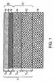
- FIGS. 1 and 2are schematic cross-sectional views of a semiconductor substrate with several semiconductor layers disposed thereon;
- FIG. 3is a schematic cross-sectional view of a semiconductor structure formed on a semiconductor substrate.
- a substrate 10is made of a semiconductor, such as silicon.
- a substrate 10is made of a semiconductor, such as silicon.
- Several layers collectively indicated at 11are formed on substrate 10 .
- Layers 11may be grown, for example, in a chemical vapor deposition (CVD) system.
- CVDchemical vapor deposition
- UHVCVDultra-high vacuum chemical vapor deposition system
- layers 11may be grown in an atmospheric pressure CVD (APCVD) system or a low pressure CVD (LPCVD) system.
- APCVDatmospheric pressure CVD
- LPCVDlow pressure CVD
- Layers 11include a graded layer 12 , disposed over substrate 10 .
- Graded layer 12may include Si and Ge with a grading rate of, for example, 10% Ge per micrometer ( ⁇ m) of thickness, and a thickness T 1 of, for example, 2-9 ⁇ m.
- Graded layer 12may be grown, for example, at 600-1100° C.
- a relaxed layer 14is disposed over graded SiGe layer 12 .
- Relaxed layer 14may include Si 1-x Ge x with a uniform composition, containing, for example, 20-90% Ge and having a thickness T 2 of, e.g., 0.2-2 ⁇ m. In an embodiment, T 2 is 1.5 ⁇ m.
- a virtual substrate 15includes relaxed layer 14 and graded layer 12 .
- compressively strained layer 16 including a semiconductor materialis disposed over relaxed layer 14 .
- compressively strained layer 16includes group IV elements, such as Si 1-y Ge y , with a Ge content (y) higher than the Ge content (x) of relaxed Si 1-x Ge x layer 14 .
- Compressively strained layer 16contains, for example, 1-100% Ge and has a thickness T 3 of, e.g., 10-500 angstroms ( ⁇ ).
- the Ge content (x) of relaxed Si 1-x Ge x layer 14may be 20-90%, and the Ge content (y) of compressively strained Si 1-y Ge y layer 16 may be 28-100%.
- compressively strained layer 16has a thickness T 3 of less than 500 ⁇ . In certain embodiments, T 3 is less than 200 ⁇ .
- compressively strained layer 16includes at least one group III and/or one group V element.
- Compressively strained layer 16may include, for example, indium gallium arsenide, indium gallium phosphide, or gallium arsenide.
- compressively strained layer 16includes at least one group II and/or one group VI element.
- Compressively strained layermay include, for example, zinc selenide, sulphur, cadmium telluride, or mercury telluride.
- a tensilely strained layer 18is disposed over compressively strained layer 16 , sharing an interface 19 with compressively strained layer 16 .
- tensilely strained layer 18is formed of silicon.
- Tensilely stiained layer 18has a thickness T 4 of, for example, 50- 300 ⁇ . In an embodiment, thickness T 4 is approximately 200 ⁇ .
- Substrate 10 with layers 11typically has a threading dislocation density of 10 5 /cm 2 .
- tensilely strained Si layer 18may be deposited by the use of a silane (SiH 4 ) source gas. Adequate growth rates, i.e., >0.01 ⁇ /s with SiH 4 , may be attained at 550° C.
- germane (GeH 4 ) and SiH 4maybe used to deposit compressively strained Si 1-y Ge y layer 16 .
- GeH 4decomposes at approximately 400° C.
- compressively strained Si 1-y Ge y layer 16may need to be maintained at a relatively low temperature, i.e., less than the 550° C. temperature needed for subsequently achieving rapid Si deposition rates with SiH 4 to form tensilely strained Si layer 18 .
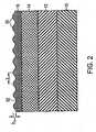
- the 4% difference in lattice constants of Si and Gemay lead to undulations 50 in a top surface 52 of compressively strained Si 1-y Ge y layer 16 , particularly if the Ge content y is greater than 40%, and/or when the strain of compressively strained Si 1-y Ge y layer 16 is greater than 0.25%.
- Undulations 50may form to partially accommodate the lattice mismatch between compressively strained Si 1-y Ge y layer 16 and relaxed layer 14 .
- Undulations 50may define a sinusoidal shape having a wavelength ⁇ and a height h 1 .
- Wavelength ⁇ and height h 1may depend on the Ge content of compressively strained Si 1-y Ge y layer 16 , the lattice mismatch between compressively strained Si 1-y Ge y layer 16 and relaxed layer 14 , and deposition conditions.
- Wavelength ⁇may be, for example, 1-100 nm
- height h 1may be several nm, e.g., 5 nm.
- the sinusoidal shape of undulations 50results in surface 52 having a surface roughness with wavelength ⁇ .
- the wavelength ⁇ of the surface roughnessis greater than a wavelength of a carrier in compressively strained Si 1-y Ge y layer 16 . The surface roughness, therefore, does not reduce carrier mobility in compressively strained Si 1-y Ge y layer 16 .
- a compressively strained Si 1-y Ge y layer 16 that is substantially planarmay be grown as follows.
- Compressively sited Si 1-y Ge y layer 16may be deposited at a first temperature low enough to enable formation of planar Si 1-y Ge y layers but not low enough to provide a suitably high deposition rate for tensilely strained Si layer 18 .
- this deposition temperature for compressively strained Si 1-y Ge y layer 16may be, e.g., 400° C.
- the tensilely strained Si layer 18may then be deposited in a two-step process.
- the silicon source gase.g., SiH 4
- the growth temperatureis slowly raised from a relatively low temperature, e.g., 400° C., to a final desired temperature in which the silicon growth rate is acceptably high.
- the final desired temperaturemay be, e.g., >450° C., such as 550° C., for UHVCVD using SiH 4 source gas.
- This stepallows enough silicon to deposit at a low temperature to help stabilize the compressively strained Si 1-y Ge y layer 16 against strain-induced undulations, as explained below.
- deposition of tensilely strained layer 18may be completed at a faster rate at a second deposition temperature, e.g., a temperature greater than 450° C., such as 550° C., for UHVCVD using SiH 4 source gas.
- the deposition rate of tensilely strained layer 18may be greater than 100 ⁇ /hour.
- Another possible result of forming a substantially planar compressively strained Si 1-y Ge y layer 16is an increase in wavelength ⁇ of surface 52 of compressively strained Si 1-y Ge y layer 16 .
- the increase in planaritymay also be accompanied by a reduction in height h 1 of undulations to, e.g., less than 10 nm.
- compressively strained layer 16has a surface roughness with wavelength ⁇ greater than a wavelength of a carrier in compressively strained layer 16 , e.g., greater than 10 nm.
- a possible mechanism for formation of tensilely strained Si layer 18may be as follows.
- surface 52 of compressively strained Si 1-y Ge y layer 16is initially passivated by hydrogen atoms bonding to silicon and germanium during CVD when exposed to a hydrogen-containing source gas, such as SiH 4 .
- the bond of hydrogen atoms to germaniumis relatively weak in comparison to the bond of hydrogen atoms to silicon.
- This bond strength differenceis manifested, e.g., in the difference in the activation energy of decomposition of silane in UHVCVD (i.e., 2.22 eV) in comparison to the activation energy of decomposition of germane in UHVCVD (i.e., 1.68 eV).
- a surface exchangetakes place in Which a silicon atom from the SiH 4 source gas exchanges bonds to hydrogen with a germanium atom from compressively strained Si 1-y Ge y layer 16 .
- the silicon atomthereby adheres to surface 52 of compressively strained Si 1-y Ge y layer 16 , beginning formation of tensilely strained layer 18 .
- a relatively fast growth rate of tensilely strained layer 18may be attained at the relatively low temperature of approximately 400° C. because the exchange of Ge—H bonds with Si—H bonds is energetically favored and Ge atoms are directly at surface 52 , or are relatively close to surface 52 . Deposition at a higher temperature, however, may cause surface 52 to buckle excessively, resulting in undulations 50 with unacceptably short wavelength ⁇ and/or high height h 1 . As SiH 4 continues to flow and more Si atoms are deposited on surface 52 by exchange with Ge atoms, the deposition temperature may be raised. Buckling of surface 52 due to exposure to higher temperatures is prevented by the deposited Si atoms forming tensilely strained layer 18 .
- the deposited Si atomsphysically suppress buckling of surface 52 .
- tensilely strained layer 18becomes thicker, there is an increase in a migration path distance that Ge atoms in compressively strained Si 1-y Ge y layer 16 need to traverse to reach surface 52 .
- This increase in Ge migration path distancebecomes prohibitive, even at higher temperatures, resulting in Ge segregation from tensilely strained Si layer 18 and allowing the deposition of tensilely stined Si layer 18 , substantially free of Ge.
- the flow of SiH 4may be stopped during the increase in temperature, after the formation of a thin tensilely strained Si layer 18 . Tlie SiH 4 flow may then be resumed when the deposition system reaches the desired higher temperature.
- a substantially planar compressively strained Si 1-y Ge y layer 16may be formed, with compressively strained Si 1-y Ge y layer 16 having a strain greater than 1%, by using the two-step silicon deposition process described above.
- compressively strained layer 16may be formed as follows. Compressively strained Si 1-y Ge y . layer 16 having a relatively low Ge content is deposited on relaxed Si 1-y Ge y layer 14 , e.g., y ⁇ 0.4-0.6, under relatively light compressive strain, e.g., y-x ⁇ 0.2.
- device layers 20including compressively strained Si 1-y Ge y layer 16 and tensilely strained Si layer 18 , may be deposited at a temperature that permits deposition of planar compressively strained Si 1-y Ge y layer 16 and simultaneously provides an acceptably high growth rate, e.g., >0.01 ⁇ /s, for tensilely strained Si layer 18 . This temperature may be, e.g., 550° C. in ultrahigh vacuum chemical vapor deposition using SiH 4 and GeH 4 source gases.
- a first transistor 60 and a second transistor 62may be formed over a substantially planar compressively strained semiconductor layer 16 having a strain greater than or equal to 0.25%.
- Tensilely strained semiconductor layer 18is disposed over compressively strained layer 16 .
- First transistor 60includes a first gate dielectric portion 64 disposed over a first portion 66 of compressively strained semiconductor layer 16 .
- First dielectric portion 64may be formed of a dielectric such as, e.g., silicon dioxide.
- a first gate 68is disposed over first gate dielectric portion 64 .
- First gate 68includes a first conducting layer, such as, e.g., doped polysilicon.
- First transistor 60also includes a first source 70 and a first drain 72 (defined for purposes of illustration by the interior boundaries), disposed proximate first gate 68 and extending into compressively strained layer 16 .
- first transistor 60is a PMOS field-effect transistor, and first source 70 and first drain 72 are formed by the introduction of p-type dopants, such as boron.
- first transistor 60is an NMOS field-effect transistor, and first source 70 and first drain 72 are formed by the introduction of n-type dopants, such as phosphorus or arsenic.
- Second transistor 62includes a second gate dielectric portion 74 disposed over second portion 76 of compressively strained semiconductor layer 16 .
- Second dielectric portion 74may be formed of a dielectric such as, e.g., silicon dioxide.
- a second gate 78is disposed over second gate dielectric portion 74 .
- Second gate 78includes a second conducting layer, such as, e.g., doped polysilicon.
- Second transistor 62also includes a second source 80 and a second drain 82 (defined for purposes of illustration by the interior boundaries), disposed proximate second gate 78 and extending into compressively strained layer 16 .
- Second transistor 62may be an NMOS field-effect transistor.
- Second source 80 and second drain 82may be formed by the introduction of n-type dopants, such as phosphorus or arsenic.
- first transistor 60is a PMOS field-effect transistor with first source 70 and first drain 72 including p-type dopants
- second transistor 62is an NMOS. field-effect transistor with second source 80 and second drain 82 including n-type dopants.
- first transistor 60 and second transistor 62form a complementary metal-oxide-semiconductor (CMOS) device.
- CMOScomplementary metal-oxide-semiconductor
- first and second transistors 60 , 62are enhanced by the use of substrate 10 with a substantially planar compressively strained semiconductor layer 16 .
- the planarity of compressively strained semiconductor layer 16enhances mobility of carriers within compressively strained layer 16 , thereby enabling faster speeds during operation of first and second transistors 60 , 62 .
Landscapes
- Insulated Gate Type Field-Effect Transistor (AREA)
- Recrystallisation Techniques (AREA)
- Metal-Oxide And Bipolar Metal-Oxide Semiconductor Integrated Circuits (AREA)
Abstract
Description
- This application claims the benefit of U.S. Provisional Application No. 60/310,346, filed Aug. 6, 2001, the entire disclosure of which is hereby incorporated by reference herein.
- This invention relates generally to semiconductor substrates and particularly to semiconductor substrates with strained layers.
- The recent development of silicon (Si) substrates with strained layers has increased the options available for design and fabrication of field-effect transistors (FETs). Enhanced performance of n-type metal-oxide-semiconductor (NMOS) transistors has been demonstrated with heterojunction metal-oxide-semiconductor field effect transistors (MOSFETs) built on substrates having strained silicon and relaxed silicon-germanium (SiGe) layers. Tensilely strained silicon significantly enhances electron mobilities. NMOS devices with strained silicon surface channels, therefore, exhibit improved performance with higher switching speeds. Hole mobilities are enhanced in tensilely stained silicon as well, but to a lesser extent for strain levels less than approximately 1.5%. Accordingly, equivalent enhancement of p-type metal-oxide-semiconductor (PMOS) device performance in such surface-channel devices presents a challenge.
- Hole mobility enhancement has been demonstrated in highly strained SiGe layers. The formation of such highly strained layers is made difficult by the tendency of these layers to undulate, especially with increasing strain levels, i.e., with high Ge content. This undulation lowers hole mobilities, thereby offsetting the beneficial mobility enhancement provided by the stained layers.
- The observed undulation arises from lattice mismatch with respect to an underlying layer, and increases in severity with formation temperature. Unfortunately, the formation of a tensilely strained layer made of, for example, Si, over the compressively strained layer is desirably carried out at a relatively high temperature, e.g., 550° C., to achieve a commercially viable formation rate and uniformity.
- The present invention facilitates-formation of the tensilely strained layer at a relatively high average temperature, while keeping the compressively strained layer substantially planar. In accordance with the invention, the tensilely strained layer is initially grown at a relatively low temperature (i.e., sufficiently low to avoid undulations in the compressively strained layer) until a thin layer of the tensilely strained layer has been formed. It is found that this thin layer suppresses undulation in the compressively strained layer even at higher process temperatures that would ordinarily induce such undulation. As a result, formation of the tensilely strained layer may continue at these higher temperatures without sacrificing planarity.
- In one aspect, therefore, the invention features a method for forming a structure based on forming a compressively strained semiconductor layer having a strain greater than or equal to 0.25%. A tensilely strained semiconductor layer is formed over the compressively strained layer. The compressively strained layer is substantially planar, having a surface roughness characterized by at least one of (i) an average roughness wavelength greater than an average wavelength of a carrier in the compressively strained layer and (ii) an average roughness height less than 10 nm.
- One or more of the following features may also be included. The compressively strained layer may include at least one group IV element, such as at least one of silicon and germanium. The compressively strained layer may include >1% germanium. The tensilely strained layer may include silicon. The compressively strained layer may include at least one of a group III and a group V element. The compressively strained layer may include indium gallium arsenide, indium gallium phosphide, and/or gallium arsenide. The compressively strained layer may include at least one of a group II and a group VI element. The compressively strained layer may include zinc selenide, sulphur, cadmium telluride, and/or mercury telluride. The compressively strained layer may have a thickness of less than 500 Å, including less than 200 Å.
- The compressively strained layer may be formed at a first temperature, and at least a portion of the tensilely stained layer may be formed at a second temperature, with the second temperature being greater than the first temperature. The tensilely strained layer may include silicon and the second temperature may be greater than 450° C. A first portion of the tensilely strained layer may be formed at a first temperature and a second portion of the tensilely strained layer may be formed at the second temperature, the first temperature being sufficiently low to substantially avoid disruption of planarity, with the first portion of the tensilely strained layer maintaining the planarity of the compressively strained layer notwithstanding transition to the second temperature.
- The tensilely strained layer may be formed at a rate greater than 100 Å/hour. The compressively strained layer and/or the tensilely strained layer may formed by chemical vapor deposition. The wavelength of the surface roughness may be greater than 10 nanometers (nm).
- In another aspect, the invention features a structure including a compressively strained semiconductor layer having a strain greater than or equal to 0.25% and a tensilely strained semiconductor layer disposed over the compressively strained layer. The compressively strained layer is substantially planar, having a surface roughness characterized by at least one of (i) an average roughness wavelength greater than an average wavelength of a carrier in the compressively strained layer and (ii) an average roughness height less than 10 nm.
- One or more of the following features may also be included. The compressively strained layer may include a group IV element, such as at least one of silicon and germanium. The strain of the compressively strained layer may be greater than 1%. The compressively strained layer may have a thickness of less than 500 Å, including less than 200 Å. The wavelength of the surface roughness may be greater than 10 nm. The tensilely strained layer may include silicon.
- The compressively strained layer may include at least one of a group III and a group V element. For example, the compressively strained layer may include indium gallium arsenide, indium gallium phosphide, and/or gallium arsenide.
- The compressively strained layer may include at least one of a group II and a group VI element For example, the compressively strained layer may include zinc selenide, sulphur, cadmium telluride, and/or mercury telluride.
- The structure may also include a first transistor formed over the compressively strained layer. The first transistor may include a first gate dielectric portion disposed over a first portion of the compresssively strained layer, a first gate disposed over the first gate dielectric portion, the first gate comprising a first conducting layer, and a first source and a first drain disposed proximate the first gate and extending into the compressively strained layer. The first transistor may be an n-type metal-oxide-semiconductor field-effect transistor and the first source and first drain may include n-type dopants. The first transistor may be a p-type metal-oxide-semiconductor field-effect transistor and the first source and first drain may include p-type dopants.
- The structure may also include a second transistor formed over the. compressively strained layer. The second transistor may include a second gate dielectric portion disposed over a second portion of the compresssively strained layer, a second gate disposed over the second gate dielectric portion, the second gate including a second conducting layer, and a second source and a second drain disposed proximate the second gate and extending into the compressively strained layer. The first transistor may be an n-type metal-oxide-semiconductor field-effect transistor, with the first source and first drain including n-type dopants, and the second transistor may be a p-type metal-oxide-semiconductor field-effect transistor, with the second source and second drain including p-type dopants.
FIGS. 1 and 2 are schematic cross-sectional views of a semiconductor substrate with several semiconductor layers disposed thereon; andFIG. 3 is a schematic cross-sectional view of a semiconductor structure formed on a semiconductor substrate.- Referring to
FIG. 1 , which illustrates a structure amenable to use with the present invention, asubstrate 10 is made of a semiconductor, such as silicon. Several layers collectively indicated at11 are formed onsubstrate 10.Layers 11 may be grown, for example, in a chemical vapor deposition (CVD) system. In some embodiments,layers 11 are grown in an ultra-high vacuum chemical vapor deposition system (UHVCVD). In certain other embodiments, layers11 may be grown in an atmospheric pressure CVD (APCVD) system or a low pressure CVD (LPCVD) system. Layers 11 include a gradedlayer 12, disposed oversubstrate 10. Gradedlayer 12 may include Si and Ge with a grading rate of, for example, 10% Ge per micrometer (μm) of thickness, and a thickness T1of, for example, 2-9 μm. Gradedlayer 12 may be grown, for example, at 600-1100° C. Arelaxed layer 14 is disposed over gradedSiGe layer 12.Relaxed layer 14 may include Si1-xGexwith a uniform composition, containing, for example, 20-90% Ge and having a thickness T2of, e.g., 0.2-2 μm. In an embodiment, T2is 1.5 μm. Avirtual substrate 15 includesrelaxed layer 14 and gradedlayer 12.- A compressively
strained layer 16 including a semiconductor material is disposed overrelaxed layer 14. In an embodiment, compressivelystrained layer 16 includes group IV elements, such as Si1-yGey, with a Ge content (y) higher than the Ge content (x) of relaxed Si1-xGexlayer14. Compressivelystrained layer 16 contains, for example, 1-100% Ge and has a thickness T3of, e.g., 10-500 angstroms (Å). The Ge content (x) of relaxed Si1-xGexlayer14 may be 20-90%, and the Ge content (y) of compressively strained Si1-yGeylayer16 may be 28-100%. In some embodiments, compressivelystrained layer 16 has a thickness T3of less than 500 Å. In certain embodiments, T3is less than 200 Å. - In some embodiments, compressively
strained layer 16 includes at least one group III and/or one group V element. Compressivelystrained layer 16 may include, for example, indium gallium arsenide, indium gallium phosphide, or gallium arsenide. - In alternative embodiments, compressively
strained layer 16 includes at least one group II and/or one group VI element. Compressively strained layer may include, for example, zinc selenide, sulphur, cadmium telluride, or mercury telluride. - A tensilely
strained layer 18 is disposed over compressivelystrained layer 16, sharing aninterface 19 with compressivelystrained layer 16. In an embodiment, tensilelystrained layer 18 is formed of silicon.Tensilely stiained layer 18 has a thickness T4of, for example, 50-300 Å. In an embodiment, thickness T4is approximately 200 Å. Substrate 10 withlayers 11 typically has a threading dislocation density of 105/cm2.- The requirements for attaining a substantially planar compressively strained Si1-yGeylayer16 and an acceptably high growth rate for tensilely
strained Si layer 18 formed by CVD are sometimes mutually exclusive. For example, a high growth rate of tensilelystrained Si layer 18 is more readily achieved by deposition at high CVD temperatures. Further, higher CVD temperatures reduce the incorporation of impurities and improve layer uniformity. More specifically, tensilelystrained Si layer 18 may be deposited by the use of a silane (SiH4) source gas. Adequate growth rates, i.e., >0.01 Å/s with SiH4, may be attained at 550° C. On the other hand, germane (GeH4) and SiH4maybe used to deposit compressively strained Si1-yGeylayer16. GeH4decomposes at approximately 400° C. To remain planar after deposition, compressively strained Si1-yGeylayer16 may need to be maintained at a relatively low temperature, i.e., less than the 550° C. temperature needed for subsequently achieving rapid Si deposition rates with SiH4to form tensilelystrained Si layer 18. - As a result, maintaining adequate planarity of compressively strained Si1-yGeylayer16 is a challenge, particularly with high Ge content, i.e., with y>40%. Si has a lattice constant of 5.431 Å and Ge has a lattice constant of 5.658 Å. The lattice mismatch between Si and Ge, therefore, is approximately 4%. Because of this lattice mismatch, a high Ge content leads to high compressive-strain in compressively strained Si1-yGeylayer16. High compressive strain may be desirable for attaining high carrier mobilities in subsequently fabricated devices.
- Referring to
FIG. 2 , the 4% difference in lattice constants of Si and Ge may lead toundulations 50 in atop surface 52 of compressively strained Si1-yGeylayer16, particularly if the Ge content y is greater than 40%, and/or when the strain of compressively strained Si1-yGeylayer16 is greater than 0.25%.Undulations 50 may form to partially accommodate the lattice mismatch between compressively strained Si1-yGeylayer16 andrelaxed layer 14.Undulations 50 may define a sinusoidal shape having a wavelength λ and a height h1. Wavelength λ and height h1may depend on the Ge content of compressively strained Si1-yGeylayer16, the lattice mismatch between compressively strained Si1-yGeylayer16 andrelaxed layer 14, and deposition conditions. Wavelength λ may be, for example, 1-100 nm, and height h1may be several nm, e.g., 5 nm. The sinusoidal shape ofundulations 50 results insurface 52 having a surface roughness with wavelength λ. In an embodiment, the wavelength λ of the surface roughness is greater than a wavelength of a carrier in compressively strained Si1-yGeylayer16. The surface roughness, therefore, does not reduce carrier mobility in compressively strained Si1-yGeylayer16. - Referring to
FIG. 2 and also toFIG. 1 , a compressively strained Si1-yGeylayer16 that is substantially planar may be grown as follows. Compressively stied Si1-yGeylayer16 may be deposited at a first temperature low enough to enable formation of planar Si1-yGeylayers but not low enough to provide a suitably high deposition rate for tensilelystrained Si layer 18. In the case of compressively strained Si1-yGeylayer16 having a relatively high strain, e.g., greater than 0.25% and/or with y>40%, this deposition temperature for compressively strained Si1-yGeylayer16 may be, e.g., 400° C. for UHVCVD using SiH4and GeH4source gases. The tensilely strainedSi layer 18 may then be deposited in a two-step process. During the first step, the silicon source gas, e.g., SiH4, is flowed while the growth temperature is slowly raised from a relatively low temperature, e.g., 400° C., to a final desired temperature in which the silicon growth rate is acceptably high. The final desired temperature may be, e.g., >450° C., such as 550° C., for UHVCVD using SiH4source gas. This step allows enough silicon to deposit at a low temperature to help stabilize the compressively strained Si1-yGeylayer16 against strain-induced undulations, as explained below. Second, deposition of tensilelystrained layer 18 may be completed at a faster rate at a second deposition temperature, e.g., a temperature greater than 450° C., such as 550° C., for UHVCVD using SiH4source gas. The deposition rate of tensilelystrained layer 18 may be greater than 100 Å/hour. Another possible result of forming a substantially planar compressively strained Si1-yGeylayer16 is an increase in wavelength λ ofsurface 52 of compressively strained Si1-yGeylayer16. The increase in planarity may also be accompanied by a reduction in height h1of undulations to, e.g., less than 10 nm. After deposition of tensilelystrained layer 18, compressivelystrained layer 16 has a surface roughness with wavelength λ greater than a wavelength of a carrier in compressivelystrained layer 16, e.g., greater than 10 nm. - A possible mechanism for formation of tensilely
strained Si layer 18, deposited as described above, may be as follows. During the first step of the deposition of tensilelystrained Si layer 18,surface 52 of compressively strained Si1-yGeylayer16 is initially passivated by hydrogen atoms bonding to silicon and germanium during CVD when exposed to a hydrogen-containing source gas, such as SiH4. The bond of hydrogen atoms to germanium, however, is relatively weak in comparison to the bond of hydrogen atoms to silicon. This bond strength difference is manifested, e.g., in the difference in the activation energy of decomposition of silane in UHVCVD (i.e., 2.22 eV) in comparison to the activation energy of decomposition of germane in UHVCVD (i.e., 1.68 eV). After passivation ofsurface 52, a surface exchange takes place in Which a silicon atom from the SiH4source gas exchanges bonds to hydrogen with a germanium atom from compressively strained Si1-yGeylayer16. The silicon atom thereby adheres to surface52 of compressively strained Si1-yGeylayer16, beginning formation of tensilelystrained layer 18. Initially, a relatively fast growth rate of tensilelystrained layer 18 may be attained at the relatively low temperature of approximately 400° C. because the exchange of Ge—H bonds with Si—H bonds is energetically favored and Ge atoms are directly atsurface 52, or are relatively close tosurface 52. Deposition at a higher temperature, however, may causesurface 52 to buckle excessively, resulting inundulations 50 with unacceptably short wavelength λ and/or high height h1. As SiH4continues to flow and more Si atoms are deposited onsurface 52 by exchange with Ge atoms, the deposition temperature may be raised. Buckling ofsurface 52 due to exposure to higher temperatures is prevented by the deposited Si atoms forming tensilelystrained layer 18. Specifically; the deposited Si atoms physically suppress buckling ofsurface 52. As tensilelystrained layer 18 becomes thicker, there is an increase in a migration path distance that Ge atoms in compressively strained Si1-yGeylayer16 need to traverse to reachsurface 52. This increase in Ge migration path distance becomes prohibitive, even at higher temperatures, resulting in Ge segregation from tensilelystrained Si layer 18 and allowing the deposition of tensilely stined Silayer 18, substantially free of Ge. Consequently, initially depositing tensilelystrained Si layer 18 at a relatively low temperature retards subsequent undulation formation, thereby facilitating completion of the deposition of tensilely strained Si layer at a higher temperature while maintaining the planarity of compressivelystrained layer 16. - In an alternative embodiment, during the first step of the deposition of tensilely
strained Si layer 18, the flow of SiH4may be stopped during the increase in temperature, after the formation of a thin tensilelystrained Si layer 18. Tlie SiH4flow may then be resumed when the deposition system reaches the desired higher temperature. - In some embodiments, a substantially planar compressively strained Si1-yGeylayer16 may be formed, with compressively strained Si1-yGeylayer16 having a strain greater than 1%, by using the two-step silicon deposition process described above.
- In another embodiment, compressively
strained layer 16 may be formed as follows. Compressively strained Si1-yGey.layer 16 having a relatively low Ge content is deposited on relaxed Si1-yGeylayer14, e.g., y˜0.4-0.6, under relatively light compressive strain, e.g., y-x≈0.2. In this embodiment, device layers20, including compressively strained Si1-yGeylayer16 and tensilelystrained Si layer 18, may be deposited at a temperature that permits deposition of planar compressively strained Si1-yGeylayer16 and simultaneously provides an acceptably high growth rate, e.g., >0.01 Å/s, for tensilelystrained Si layer 18. This temperature may be, e.g., 550° C. in ultrahigh vacuum chemical vapor deposition using SiH4and GeH4source gases. - Referring to
FIG. 3 as well as toFIGS. 1 and 2 , afirst transistor 60 and asecond transistor 62 may be formed over a substantially planar compressivelystrained semiconductor layer 16 having a strain greater than or equal to 0.25%. Tensilelystrained semiconductor layer 18 is disposed over compressivelystrained layer 16.First transistor 60 includes a firstgate dielectric portion 64 disposed over afirst portion 66 of compressivelystrained semiconductor layer 16. Firstdielectric portion 64 may be formed of a dielectric such as, e.g., silicon dioxide. Afirst gate 68 is disposed over firstgate dielectric portion 64.First gate 68 includes a first conducting layer, such as, e.g., doped polysilicon.First transistor 60 also includes afirst source 70 and a first drain72 (defined for purposes of illustration by the interior boundaries), disposed proximatefirst gate 68 and extending into compressivelystrained layer 16. In an embodiment,first transistor 60 is a PMOS field-effect transistor, andfirst source 70 andfirst drain 72 are formed by the introduction of p-type dopants, such as boron. In an alternative embodiment,first transistor 60 is an NMOS field-effect transistor, andfirst source 70 andfirst drain 72 are formed by the introduction of n-type dopants, such as phosphorus or arsenic. Second transistor 62 includes a secondgate dielectric portion 74 disposed oversecond portion 76 of compressivelystrained semiconductor layer 16.Second dielectric portion 74 may be formed of a dielectric such as, e.g., silicon dioxide. Asecond gate 78 is disposed over secondgate dielectric portion 74.Second gate 78 includes a second conducting layer, such as, e.g., doped polysilicon.Second transistor 62 also includes asecond source 80 and a second drain82 (defined for purposes of illustration by the interior boundaries), disposed proximatesecond gate 78 and extending into compressivelystrained layer 16.Second transistor 62 may be an NMOS field-effect transistor.Second source 80 andsecond drain 82 may be formed by the introduction of n-type dopants, such as phosphorus or arsenic.- In an embodiment,
first transistor 60 is a PMOS field-effect transistor withfirst source 70 andfirst drain 72 including p-type dopants, andsecond transistor 62 is an NMOS. field-effect transistor withsecond source 80 andsecond drain 82 including n-type dopants. Together,first transistor 60 andsecond transistor 62 form a complementary metal-oxide-semiconductor (CMOS) device. - The functionality of first and
second transistors substrate 10 with a substantially planar compressivelystrained semiconductor layer 16. The planarity of compressivelystrained semiconductor layer 16 enhances mobility of carriers within compressivelystrained layer 16, thereby enabling faster speeds during operation of first andsecond transistors - The invention may be embodied in other specific forms without departing from the spirit of essential characteristics thereof. The foregoing embodiments are therefore to be considered in all respects illustrative rather than limiting on the invention described herein. Scope of the invention is thus indicated by the appended claims rather than by the foregoing description, and all changes which come within the meaning and range of equivalency of the claims are intended to be embraced herein.
Claims (20)
1.-47. (canceled)
48. A method for forming a structure, the method comprising:
defining a p-type metal-oxide-semiconductor field-effect transistor (PMOSFET) over a substrate, the PMOSFET including:
a first source and a first drain, defining a first channel therebetween and each of the first source and first drain comprising p-type dopants,
a first gate disposed above the first channel, the first gate comprising a first conducting layer, and
a first gate dielectric layer disposed between the first gate and the first channel,
wherein the first source and the first drain each comprises compressively strained SiGe having a strain greater than or equal to 0.25%, and the compressively strained SiGe is substantially planar.
49. The method ofclaim 48 , wherein the first channel comprises a first strained semiconductor.
50. The method ofclaim 49 , wherein a Ge content of the compressively strained SiGe is selected from a range of approximately 28% to approximately 100%.
51. The method ofclaim 49 , wherein the compressively strained SiGe has an average roughness height less than 10 nm.
52. The method ofclaim 49 , wherein a strain of the compressively strained SiGe is greater than approximately 1%.
53. The method ofclaim 49 , wherein the substrate consists essentially of silicon.
54. The method ofclaim 49 , further comprising:
defining an n-type metal-oxide-semiconductor field-effect transistor (NMOSFET) over the substrate, the NMOSFET including:
a second source and a second drain, defining a second channel therebetween and each of the second source and second drain comprising n-type dopants,
a second gate disposed above the second channel, the second gate comprising a second conducting layer, and
a second gate dielectric layer disposed between the second gate and the second channel,
wherein the second channel comprises a second strained semiconductor.
55. The method ofclaim 54 , wherein the second strained semiconductor is tensilely strained.
56. The method ofclaim 55 , wherein the second strained semiconductor comprises silicon.
57. The method ofclaim 56 , wherein the second strained semiconductor consists essentially of silicon.
58. The method ofclaim 56 , wherein the second strained semiconductor is substantially free of germanium.
59. The method ofclaim 56 , wherein the second source and the second drain each comprises a silicon layer substantially free of germanium.
60. The method ofclaim 56 , wherein the PMOSFET and NMOSFET form a complementary metal-oxide-semiconductor (CMOS) device.
61. The method ofclaim 49 , wherein the first strained semiconductor is compressively strained.
62. The method ofclaim 61 , further comprising:
defining an n-type metal-oxide-semiconductor field-effect transistor (NMOSFET) over the substrate, the NMOSFET including:
a second source and a second drain, defining a second channel therebetween and each of the second source and second drain comprising n-type dopants,
a second gate disposed above the second channel, the second gate comprising a second conducting layer, and
a second gate dielectric layer disposed between the second gate and the second channel,
wherein the second channel comprises a second strained semiconductor.
63. The method ofclaim 62 , wherein the second strained semiconductor is tensilely strained.
64. The method ofclaim 63 , wherein the second strained semiconductor comprises silicon.
65. The method ofclaim 64 , wherein the second strained semiconductor consists essentially of silicon.
66. The method ofclaim 64 , wherein the second strained semiconductor is substantially free of germanium.67. The method ofclaim 64 , wherein the second source and the second drain each comprises a silicon layer substantially free of germanium.
Priority Applications (1)
| Application Number | Priority Date | Filing Date | Title |
|---|---|---|---|
| US11/584,181US20070072354A1 (en) | 2001-08-06 | 2006-10-20 | Structures with planar strained layers |
Applications Claiming Priority (4)
| Application Number | Priority Date | Filing Date | Title |
|---|---|---|---|
| US31034601P | 2001-08-06 | 2001-08-06 | |
| US10/211,126US6730551B2 (en) | 2001-08-06 | 2002-08-02 | Formation of planar strained layers |
| US10/788,741US7141820B2 (en) | 2001-08-06 | 2004-02-27 | Structures with planar strained layers |
| US11/584,181US20070072354A1 (en) | 2001-08-06 | 2006-10-20 | Structures with planar strained layers |
Related Parent Applications (1)
| Application Number | Title | Priority Date | Filing Date |
|---|---|---|---|
| US10/788,741ContinuationUS7141820B2 (en) | 2001-08-06 | 2004-02-27 | Structures with planar strained layers |
Publications (1)
| Publication Number | Publication Date |
|---|---|
| US20070072354A1true US20070072354A1 (en) | 2007-03-29 |
Family
ID=23202088
Family Applications (3)
| Application Number | Title | Priority Date | Filing Date |
|---|---|---|---|
| US10/211,126Expired - Fee RelatedUS6730551B2 (en) | 2001-08-06 | 2002-08-02 | Formation of planar strained layers |
| US10/788,741Expired - Fee RelatedUS7141820B2 (en) | 2001-08-06 | 2004-02-27 | Structures with planar strained layers |
| US11/584,181AbandonedUS20070072354A1 (en) | 2001-08-06 | 2006-10-20 | Structures with planar strained layers |
Family Applications Before (2)
| Application Number | Title | Priority Date | Filing Date |
|---|---|---|---|
| US10/211,126Expired - Fee RelatedUS6730551B2 (en) | 2001-08-06 | 2002-08-02 | Formation of planar strained layers |
| US10/788,741Expired - Fee RelatedUS7141820B2 (en) | 2001-08-06 | 2004-02-27 | Structures with planar strained layers |
Country Status (4)
| Country | Link |
|---|---|
| US (3) | US6730551B2 (en) |
| EP (1) | EP1415331A2 (en) |
| JP (1) | JP2004538634A (en) |
| WO (1) | WO2003015142A2 (en) |
Cited By (6)
| Publication number | Priority date | Publication date | Assignee | Title |
|---|---|---|---|---|
| US20050151164A1 (en)* | 2001-06-21 | 2005-07-14 | Amberwave Systems Corporation | Enhancement of p-type metal-oxide-semiconductor field effect transistors |
| US20060266997A1 (en)* | 2001-08-09 | 2006-11-30 | Amberwave Systems Corporation | Methods for forming semiconductor structures with differential surface layer thicknesses |
| US20070032009A1 (en)* | 2002-06-07 | 2007-02-08 | Amberwave Systems Corporation | Semiconductor devices having strained dual channel layers |
| US20080128747A1 (en)* | 2001-06-18 | 2008-06-05 | Lee Minjoo L | STRUCTURE AND METHOD FOR A HIGH-SPEED SEMICONDUCTOR DEVICE HAVING A Ge CHANNEL LAYER |
| US7465619B2 (en) | 2001-08-09 | 2008-12-16 | Amberwave Systems Corporation | Methods of fabricating dual layer semiconductor devices |
| US20130313613A1 (en)* | 2012-04-26 | 2013-11-28 | Asif Khan | Selectively Area Regrown III-Nitride High Electron Mobility Transistor |
Families Citing this family (70)
| Publication number | Priority date | Publication date | Assignee | Title |
|---|---|---|---|---|
| JP3535527B2 (en)* | 1997-06-24 | 2004-06-07 | マサチューセッツ インスティテュート オブ テクノロジー | Controlling threading dislocations in germanium-on-silicon using graded GeSi layer and planarization |
| US7227176B2 (en) | 1998-04-10 | 2007-06-05 | Massachusetts Institute Of Technology | Etch stop layer system |
| JP2003520444A (en)* | 2000-01-20 | 2003-07-02 | アンバーウェーブ システムズ コーポレイション | Low threading dislocation density lattice-mismatched epilayer that does not require high-temperature growth |
| US6602613B1 (en) | 2000-01-20 | 2003-08-05 | Amberwave Systems Corporation | Heterointegration of materials using deposition and bonding |
| US6573126B2 (en)* | 2000-08-16 | 2003-06-03 | Massachusetts Institute Of Technology | Process for producing semiconductor article using graded epitaxial growth |
| US6649480B2 (en)* | 2000-12-04 | 2003-11-18 | Amberwave Systems Corporation | Method of fabricating CMOS inverter and integrated circuits utilizing strained silicon surface channel MOSFETs |
| US20020100942A1 (en)* | 2000-12-04 | 2002-08-01 | Fitzgerald Eugene A. | CMOS inverter and integrated circuits utilizing strained silicon surface channel MOSFETs |
| JP2002232075A (en)* | 2001-01-31 | 2002-08-16 | Ando Electric Co Ltd | Tunable light source |
| US6830976B2 (en) | 2001-03-02 | 2004-12-14 | Amberwave Systems Corproation | Relaxed silicon germanium platform for high speed CMOS electronics and high speed analog circuits |
| US6723661B2 (en)* | 2001-03-02 | 2004-04-20 | Amberwave Systems Corporation | Relaxed silicon germanium platform for high speed CMOS electronics and high speed analog circuits |
| US6724008B2 (en) | 2001-03-02 | 2004-04-20 | Amberwave Systems Corporation | Relaxed silicon germanium platform for high speed CMOS electronics and high speed analog circuits |
| US6703688B1 (en) | 2001-03-02 | 2004-03-09 | Amberwave Systems Corporation | Relaxed silicon germanium platform for high speed CMOS electronics and high speed analog circuits |
| WO2002082514A1 (en) | 2001-04-04 | 2002-10-17 | Massachusetts Institute Of Technology | A method for semiconductor device fabrication |
| JP4831885B2 (en) | 2001-04-27 | 2011-12-07 | 株式会社半導体エネルギー研究所 | Method for manufacturing semiconductor device |
| EP1415331A2 (en)* | 2001-08-06 | 2004-05-06 | Massachusetts Institute Of Technology | Formation of planar strained layers |
| US6831292B2 (en)* | 2001-09-21 | 2004-12-14 | Amberwave Systems Corporation | Semiconductor structures employing strained material layers with defined impurity gradients and methods for fabricating same |
| US6933518B2 (en)* | 2001-09-24 | 2005-08-23 | Amberwave Systems Corporation | RF circuits including transistors having strained material layers |
| US6649492B2 (en)* | 2002-02-11 | 2003-11-18 | International Business Machines Corporation | Strained Si based layer made by UHV-CVD, and devices therein |
| WO2003079415A2 (en) | 2002-03-14 | 2003-09-25 | Amberwave Systems Corporation | Methods for fabricating strained layers on semiconductor substrates |
| US6995430B2 (en) | 2002-06-07 | 2006-02-07 | Amberwave Systems Corporation | Strained-semiconductor-on-insulator device structures |
| US20030227057A1 (en)* | 2002-06-07 | 2003-12-11 | Lochtefeld Anthony J. | Strained-semiconductor-on-insulator device structures |
| US7615829B2 (en) | 2002-06-07 | 2009-11-10 | Amberwave Systems Corporation | Elevated source and drain elements for strained-channel heterojuntion field-effect transistors |
| US7074623B2 (en)* | 2002-06-07 | 2006-07-11 | Amberwave Systems Corporation | Methods of forming strained-semiconductor-on-insulator finFET device structures |
| US7335545B2 (en)* | 2002-06-07 | 2008-02-26 | Amberwave Systems Corporation | Control of strain in device layers by prevention of relaxation |
| US7307273B2 (en)* | 2002-06-07 | 2007-12-11 | Amberwave Systems Corporation | Control of strain in device layers by selective relaxation |
| US6946371B2 (en) | 2002-06-10 | 2005-09-20 | Amberwave Systems Corporation | Methods of fabricating semiconductor structures having epitaxially grown source and drain elements |
| US6982474B2 (en) | 2002-06-25 | 2006-01-03 | Amberwave Systems Corporation | Reacted conductive gate electrodes |
| US6841457B2 (en)* | 2002-07-16 | 2005-01-11 | International Business Machines Corporation | Use of hydrogen implantation to improve material properties of silicon-germanium-on-insulator material made by thermal diffusion |
| AU2003274922A1 (en)* | 2002-08-23 | 2004-03-11 | Amberwave Systems Corporation | Semiconductor heterostructures having reduced dislocation pile-ups and related methods |
| US7594967B2 (en)* | 2002-08-30 | 2009-09-29 | Amberwave Systems Corporation | Reduction of dislocation pile-up formation during relaxed lattice-mismatched epitaxy |
| US6759712B2 (en)* | 2002-09-12 | 2004-07-06 | Micron Technology, Inc. | Semiconductor-on-insulator thin film transistor constructions |
| EP1593145A2 (en)* | 2002-10-30 | 2005-11-09 | Amberwave Systems Corporation | Methods for preserving strained semiconductor layers during oxide layer formation |
| JP4659732B2 (en)* | 2003-01-27 | 2011-03-30 | 台湾積體電路製造股▲ふん▼有限公司 | Method for forming a semiconductor layer |
| US6924181B2 (en)* | 2003-02-13 | 2005-08-02 | Taiwan Semiconductor Manufacturing Co., Ltd | Strained silicon layer semiconductor product employing strained insulator layer |
| US6911379B2 (en)* | 2003-03-05 | 2005-06-28 | Taiwan Semiconductor Manufacturing Company, Ltd. | Method of forming strained silicon on insulator substrate |
| WO2004081982A2 (en) | 2003-03-07 | 2004-09-23 | Amberwave Systems Corporation | Shallow trench isolation process |
| US6963078B2 (en)* | 2003-03-15 | 2005-11-08 | International Business Machines Corporation | Dual strain-state SiGe layers for microelectronics |
| KR100679737B1 (en)* | 2003-05-19 | 2007-02-07 | 도시바세라믹스가부시키가이샤 | Manufacturing Method of Silicon Substrate Having Distortion Layer |
| US6831350B1 (en) | 2003-10-02 | 2004-12-14 | Freescale Semiconductor, Inc. | Semiconductor structure with different lattice constant materials and method for forming the same |
| US6919258B2 (en) | 2003-10-02 | 2005-07-19 | Freescale Semiconductor, Inc. | Semiconductor device incorporating a defect controlled strained channel structure and method of making the same |
| US7037770B2 (en)* | 2003-10-20 | 2006-05-02 | International Business Machines Corporation | Method of manufacturing strained dislocation-free channels for CMOS |
| JP4413580B2 (en)* | 2003-11-04 | 2010-02-10 | 株式会社東芝 | Method for manufacturing element forming substrate |
| US7615424B2 (en)* | 2004-03-25 | 2009-11-10 | Semiconductor Energy Laboratory Co., Ltd. | Laser irradiation apparatus and method for manufacturing semiconductor device using the laser irradiation apparatus |
| US7791107B2 (en)* | 2004-06-16 | 2010-09-07 | Massachusetts Institute Of Technology | Strained tri-channel layer for semiconductor-based electronic devices |
| US7229893B2 (en)* | 2004-06-23 | 2007-06-12 | Taiwan Semiconductor Manufacturing Company, Ltd. | Method and apparatus for a semiconductor device with a high-k gate dielectric |
| US7244958B2 (en)* | 2004-06-24 | 2007-07-17 | International Business Machines Corporation | Integration of strained Ge into advanced CMOS technology |
| US7279756B2 (en)* | 2004-07-21 | 2007-10-09 | Taiwan Semiconductor Manufacturing Company, Ltd. | Semiconductor device with high-k gate dielectric and quasi-metal gate, and method of forming thereof |
| KR100674914B1 (en)* | 2004-09-25 | 2007-01-26 | 삼성전자주식회사 | Morse transistor having a modified channel layer and method of manufacturing same |
| US7393733B2 (en) | 2004-12-01 | 2008-07-01 | Amberwave Systems Corporation | Methods of forming hybrid fin field-effect transistor structures |
| US20060113603A1 (en)* | 2004-12-01 | 2006-06-01 | Amberwave Systems Corporation | Hybrid semiconductor-on-insulator structures and related methods |
| US7355235B2 (en)* | 2004-12-22 | 2008-04-08 | Taiwan Semiconductor Manufacturing Company, Ltd. | Semiconductor device and method for high-k gate dielectrics |
| US7332407B2 (en)* | 2004-12-23 | 2008-02-19 | Taiwan Semiconductor Manufacturing Company, Ltd. | Method and apparatus for a semiconductor device with a high-k gate dielectric |
| US20060157806A1 (en)* | 2005-01-18 | 2006-07-20 | Omnivision Technologies, Inc. | Multilayered semiconductor susbtrate and image sensor formed thereon for improved infrared response |
| US7465972B2 (en)* | 2005-01-21 | 2008-12-16 | Taiwan Semiconductor Manufacturing Company, Ltd. | High performance CMOS device design |
| US7268362B2 (en) | 2005-02-25 | 2007-09-11 | Taiwan Semiconductor Manufacturing Company, Ltd. | High performance transistors with SiGe strain |
| KR100703967B1 (en)* | 2005-02-28 | 2007-04-05 | 삼성전자주식회사 | CMOS transistor and its manufacturing method |
| US7470972B2 (en)* | 2005-03-11 | 2008-12-30 | Intel Corporation | Complementary metal oxide semiconductor integrated circuit using uniaxial compressive stress and biaxial compressive stress |
| KR101155097B1 (en)* | 2005-08-24 | 2012-06-11 | 삼성전자주식회사 | Fabricating method for semiconductor device and semiconductor device fabricated by the same |
| WO2007067589A2 (en)* | 2005-12-05 | 2007-06-14 | Massachusetts Institute Of Technology | Insulated gate devices and method of making same |
| US7323392B2 (en)* | 2006-03-28 | 2008-01-29 | Taiwan Semiconductor Manufacturing Company, Ltd. | High performance transistor with a highly stressed channel |
| US8063397B2 (en)* | 2006-06-28 | 2011-11-22 | Massachusetts Institute Of Technology | Semiconductor light-emitting structure and graded-composition substrate providing yellow-green light emission |
| US7648853B2 (en)* | 2006-07-11 | 2010-01-19 | Asm America, Inc. | Dual channel heterostructure |
| CN101641792B (en) | 2007-02-22 | 2012-03-21 | 富士通半导体股份有限公司 | Semiconductor device and process for producing the same |
| US7795605B2 (en)* | 2007-06-29 | 2010-09-14 | International Business Machines Corporation | Phase change material based temperature sensor |
| US8754455B2 (en) | 2011-01-03 | 2014-06-17 | International Business Machines Corporation | Junction field effect transistor structure with P-type silicon germanium or silicon germanium carbide gate(s) and method of forming the structure |
| KR20120107762A (en)* | 2011-03-22 | 2012-10-04 | 삼성전자주식회사 | Methods of fabricating semiconductor devices |
| US8828813B2 (en)* | 2012-04-13 | 2014-09-09 | Taiwan Semiconductor Manufacturing Co., Ltd. | Replacement channels |
| CN104465657B (en) | 2013-09-22 | 2017-10-20 | 中芯国际集成电路制造(上海)有限公司 | Complementary TFET and its manufacture method |
| US9379243B1 (en) | 2015-02-19 | 2016-06-28 | Intermational Business Machines Corporation | Field-effect transistor with aggressively strained fins |
| US9793403B2 (en)* | 2015-04-14 | 2017-10-17 | Samsung Electronics Co., Ltd. | Multi-layer fin field effect transistor devices and methods of forming the same |
Citations (90)
| Publication number | Priority date | Publication date | Assignee | Title |
|---|---|---|---|---|
| US4497683A (en)* | 1982-05-03 | 1985-02-05 | At&T Bell Laboratories | Process for producing dielectrically isolated silicon devices |
| US4692992A (en)* | 1986-06-25 | 1987-09-15 | Rca Corporation | Method of forming isolation regions in a semiconductor device |
| US4920076A (en)* | 1988-04-15 | 1990-04-24 | The United States Of America As Represented By The United States Department Of Energy | Method for enhancing growth of SiO2 in Si by the implantation of germanium |
| US4990979A (en)* | 1988-05-13 | 1991-02-05 | Eurosil Electronic Gmbh | Non-volatile memory cell |
| US5079447A (en)* | 1990-03-20 | 1992-01-07 | Integrated Device Technology | BiCMOS gates with improved driver stages |
| US5089872A (en)* | 1990-04-27 | 1992-02-18 | North Carolina State University | Selective germanium deposition on silicon and resulting structures |
| US5155571A (en)* | 1990-08-06 | 1992-10-13 | The Regents Of The University Of California | Complementary field effect transistors having strained superlattice structure |
| US5241197A (en)* | 1989-01-25 | 1993-08-31 | Hitachi, Ltd. | Transistor provided with strained germanium layer |
| US5242847A (en)* | 1992-07-27 | 1993-09-07 | North Carolina State University At Raleigh | Selective deposition of doped silion-germanium alloy on semiconductor substrate |
| US5291439A (en)* | 1991-09-12 | 1994-03-01 | International Business Machines Corporation | Semiconductor memory cell and memory array with inversion layer |
| US5312766A (en)* | 1991-03-06 | 1994-05-17 | National Semiconductor Corporation | Method of providing lower contact resistance in MOS transistors |
| US5327375A (en)* | 1988-07-08 | 1994-07-05 | Eliyahou Harari | DRAM cell utilizing novel capacitor |
| US5442205A (en)* | 1991-04-24 | 1995-08-15 | At&T Corp. | Semiconductor heterostructure devices with strained semiconductor layers |
| US5523592A (en)* | 1993-02-03 | 1996-06-04 | Hitachi, Ltd. | Semiconductor optical device, manufacturing method for the same, and opto-electronic integrated circuit using the same |
| US5534713A (en)* | 1994-05-20 | 1996-07-09 | International Business Machines Corporation | Complementary metal-oxide semiconductor transistor logic using strained SI/SIGE heterostructure layers |
| US5596527A (en)* | 1992-12-07 | 1997-01-21 | Nippon Steel Corporation | Electrically alterable n-bit per cell non-volatile memory with reference cells |
| US5617351A (en)* | 1992-03-12 | 1997-04-01 | International Business Machines Corporation | Three-dimensional direct-write EEPROM arrays and fabrication methods |
| US5739567A (en)* | 1992-11-02 | 1998-04-14 | Wong; Chun Chiu D. | Highly compact memory device with nonvolatile vertical transistor memory cell |
| US5777347A (en)* | 1995-03-07 | 1998-07-07 | Hewlett-Packard Company | Vertical CMOS digital multi-valued restoring logic device |
| US5780922A (en)* | 1996-11-27 | 1998-07-14 | The Regents Of The University Of California | Ultra-low phase noise GE MOSFETs |
| US5786612A (en)* | 1995-10-25 | 1998-07-28 | Mitsubishi Denki Kabushiki Kaisha | Semiconductor device comprising trench EEPROM |
| US5792679A (en)* | 1993-08-30 | 1998-08-11 | Sharp Microelectronics Technology, Inc. | Method for forming silicon-germanium/Si/silicon dioxide heterostructure using germanium implant |
| US5808344A (en)* | 1996-12-13 | 1998-09-15 | International Business Machines Corporation | Single-transistor logic and CMOS inverters |
| US5891769A (en)* | 1997-04-07 | 1999-04-06 | Motorola, Inc. | Method for forming a semiconductor device having a heteroepitaxial layer |
| US5906951A (en)* | 1997-04-30 | 1999-05-25 | International Business Machines Corporation | Strained Si/SiGe layers on insulator |
| US5951757A (en)* | 1997-05-06 | 1999-09-14 | The United States Of America As Represented By The Secretary Of The Navy | Method for making silicon germanium alloy and electric device structures |
| US6013134A (en)* | 1998-02-18 | 2000-01-11 | International Business Machines Corporation | Advance integrated chemical vapor deposition (AICVD) for semiconductor devices |
| US6058044A (en)* | 1997-12-10 | 2000-05-02 | Kabushiki Kaisha Toshiba | Shielded bit line sensing scheme for nonvolatile semiconductor memory |
| US6096590A (en)* | 1996-07-18 | 2000-08-01 | International Business Machines Corporation | Scalable MOS field effect transistor |
| US6107653A (en)* | 1997-06-24 | 2000-08-22 | Massachusetts Institute Of Technology | Controlling threading dislocation densities in Ge on Si using graded GeSi layers and planarization |
| US6111267A (en)* | 1997-05-13 | 2000-08-29 | Siemens Aktiengesellschaft | CMOS integrated circuit including forming doped wells, a layer of intrinsic silicon, a stressed silicon germanium layer where germanium is between 25 and 50%, and another intrinsic silicon layer |
| US6117750A (en)* | 1997-12-29 | 2000-09-12 | France Telecom | Process for obtaining a layer of single-crystal germanium or silicon on a substrate of single-crystal silicon or germanium, respectively |
| US6204529B1 (en)* | 1999-08-27 | 2001-03-20 | Hsing Lan Lung | 8 bit per cell non-volatile semiconductor memory structure utilizing trench technology and dielectric floating gate |
| US6207977B1 (en)* | 1995-06-16 | 2001-03-27 | Interuniversitaire Microelektronica | Vertical MISFET devices |
| US6228694B1 (en)* | 1999-06-28 | 2001-05-08 | Intel Corporation | Method of increasing the mobility of MOS transistors by use of localized stress regions |
| US6235568B1 (en)* | 1999-01-22 | 2001-05-22 | Intel Corporation | Semiconductor device having deposited silicon regions and a method of fabrication |
| US20010003364A1 (en)* | 1998-05-27 | 2001-06-14 | Sony Corporation | Semiconductor and fabrication method thereof |
| US6249022B1 (en)* | 1999-10-22 | 2001-06-19 | United Microelectronics Corp. | Trench flash memory with nitride spacers for electron trapping |
| US6251755B1 (en)* | 1999-04-22 | 2001-06-26 | International Business Machines Corporation | High resolution dopant/impurity incorporation in semiconductors via a scanned atomic force probe |
| US6281532B1 (en)* | 1999-06-28 | 2001-08-28 | Intel Corporation | Technique to obtain increased channel mobilities in NMOS transistors by gate electrode engineering |
| US6339232B1 (en)* | 1999-09-20 | 2002-01-15 | Kabushika Kaisha Toshiba | Semiconductor device |
| US6350993B1 (en)* | 1999-03-12 | 2002-02-26 | International Business Machines Corporation | High speed composite p-channel Si/SiGe heterostructure for field effect devices |
| US20020063292A1 (en)* | 2000-11-29 | 2002-05-30 | Mark Armstrong | CMOS fabrication process utilizing special transistor orientation |
| US6399970B2 (en)* | 1996-09-17 | 2002-06-04 | Matsushita Electric Industrial Co., Ltd. | FET having a Si/SiGeC heterojunction channel |
| US6407406B1 (en)* | 1998-06-30 | 2002-06-18 | Kabushiki Kaisha Toshiba | Semiconductor device and method of manufacturing the same |
| US20020100942A1 (en)* | 2000-12-04 | 2002-08-01 | Fitzgerald Eugene A. | CMOS inverter and integrated circuits utilizing strained silicon surface channel MOSFETs |
| US6437375B1 (en)* | 2000-06-05 | 2002-08-20 | Micron Technology, Inc. | PD-SOI substrate with suppressed floating body effect and method for its fabrication |
| US20020125471A1 (en)* | 2000-12-04 | 2002-09-12 | Fitzgerald Eugene A. | CMOS inverter circuits utilizing strained silicon surface channel MOSFETS |
| US20030013323A1 (en)* | 2001-06-14 | 2003-01-16 | Richard Hammond | Method of selective removal of SiGe alloys |
| US20030052334A1 (en)* | 2001-06-18 | 2003-03-20 | Lee Minjoo L. | Structure and method for a high-speed semiconductor device |
| US20030057439A1 (en)* | 2001-08-09 | 2003-03-27 | Fitzgerald Eugene A. | Dual layer CMOS devices |
| US6555839B2 (en)* | 2000-05-26 | 2003-04-29 | Amberwave Systems Corporation | Buried channel strained silicon FET using a supply layer created through ion implantation |
| US6563152B2 (en)* | 2000-12-29 | 2003-05-13 | Intel Corporation | Technique to obtain high mobility channels in MOS transistors by forming a strain layer on an underside of a channel |
| US6583437B2 (en)* | 2000-03-17 | 2003-06-24 | Kabushiki Kaisha Toshiba | Semiconductor device and method of manufacturing the same |
| US6593625B2 (en)* | 2001-06-12 | 2003-07-15 | International Business Machines Corporation | Relaxed SiGe layers on Si or silicon-on-insulator substrates by ion implantation and thermal annealing |
| US6593641B1 (en)* | 2001-03-02 | 2003-07-15 | Amberwave Systems Corporation | Relaxed silicon germanium platform for high speed CMOS electronics and high speed analog circuits |
| US6600170B1 (en)* | 2001-12-17 | 2003-07-29 | Advanced Micro Devices, Inc. | CMOS with strained silicon channel NMOS and silicon germanium channel PMOS |
| US6603156B2 (en)* | 2001-03-31 | 2003-08-05 | International Business Machines Corporation | Strained silicon on insulator structures |
| US6605498B1 (en)* | 2002-03-29 | 2003-08-12 | Intel Corporation | Semiconductor transistor having a backfilled channel material |
| US6621131B2 (en)* | 2001-11-01 | 2003-09-16 | Intel Corporation | Semiconductor transistor having a stressed channel |
| US6620664B2 (en)* | 2002-02-07 | 2003-09-16 | Sharp Laboratories Of America, Inc. | Silicon-germanium MOSFET with deposited gate dielectric and metal gate electrode and method for making the same |
| US6677192B1 (en)* | 2001-03-02 | 2004-01-13 | Amberwave Systems Corporation | Method of fabricating a relaxed silicon germanium platform having planarizing for high speed CMOS electronics and high speed analog circuits |
| US20040007724A1 (en)* | 2002-07-12 | 2004-01-15 | Anand Murthy | Process for ultra-thin body SOI devices that incorporate EPI silicon tips and article made thereby |
| US20040014276A1 (en)* | 2002-07-16 | 2004-01-22 | Murthy Anand S. | Method of making a semiconductor transistor |
| US20040026765A1 (en)* | 2002-06-07 | 2004-02-12 | Amberwave Systems Corporation | Semiconductor devices having strained dual channel layers |
| US6693641B1 (en)* | 2000-05-25 | 2004-02-17 | Intel Corporation | Calculating display mode values |
| US6703688B1 (en)* | 2001-03-02 | 2004-03-09 | Amberwave Systems Corporation | Relaxed silicon germanium platform for high speed CMOS electronics and high speed analog circuits |
| US6703648B1 (en)* | 2002-10-29 | 2004-03-09 | Advanced Micro Devices, Inc. | Strained silicon PMOS having silicon germanium source/drain extensions and method for its fabrication |
| US6723661B2 (en)* | 2001-03-02 | 2004-04-20 | Amberwave Systems Corporation | Relaxed silicon germanium platform for high speed CMOS electronics and high speed analog circuits |
| US6724008B2 (en)* | 2001-03-02 | 2004-04-20 | Amberwave Systems Corporation | Relaxed silicon germanium platform for high speed CMOS electronics and high speed analog circuits |
| US6730551B2 (en)* | 2001-08-06 | 2004-05-04 | Massachusetts Institute Of Technology | Formation of planar strained layers |
| US6737670B2 (en)* | 2000-08-16 | 2004-05-18 | Massachusetts Institute Of Technology | Semiconductor substrate structure |
| US6743684B2 (en)* | 2002-10-11 | 2004-06-01 | Texas Instruments Incorporated | Method to produce localized halo for MOS transistor |
| US20040119101A1 (en)* | 2002-12-23 | 2004-06-24 | Gerhard Schrom | Contact layout for MOSFETs under tensile strain |
| US20050017236A1 (en)* | 1999-03-30 | 2005-01-27 | Hitachi, Ltd. | Semiconductor device and semiconductor substrate |
| US6916694B2 (en)* | 2003-08-28 | 2005-07-12 | International Business Machines Corporation | Strained silicon-channel MOSFET using a damascene gate process |
| US20050151164A1 (en)* | 2001-06-21 | 2005-07-14 | Amberwave Systems Corporation | Enhancement of p-type metal-oxide-semiconductor field effect transistors |
| US6921913B2 (en)* | 2003-03-04 | 2005-07-26 | Taiwan Semiconductor Manufacturing Co., Ltd. | Strained-channel transistor structure with lattice-mismatched zone |
| US6940089B2 (en)* | 2001-04-04 | 2005-09-06 | Massachusetts Institute Of Technology | Semiconductor device structure |
| US6943087B1 (en)* | 2003-12-17 | 2005-09-13 | Advanced Micro Devices, Inc. | Semiconductor on insulator MOSFET having strained silicon channel |
| US7001837B2 (en)* | 2003-01-17 | 2006-02-21 | Advanced Micro Devices, Inc. | Semiconductor with tensile strained substrate and method of making the same |
| US20060071285A1 (en)* | 2004-09-29 | 2006-04-06 | Suman Datta | Inducing strain in the channels of metal gate transistors |
| US7033869B1 (en)* | 2004-01-13 | 2006-04-25 | Advanced Micro Devices | Strained silicon semiconductor on insulator MOSFET |
| US7083998B2 (en)* | 1998-03-02 | 2006-08-01 | International Business Machines Corporation | Si/SiGe optoelectronic integrated circuits |
| US7161206B2 (en)* | 2004-04-12 | 2007-01-09 | Samsung Electronics Co., Ltd. | Non-volatile memory devices |
| US7163853B2 (en)* | 2005-02-09 | 2007-01-16 | Taiwan Semiconductor Manufacturing Company, Ltd. | Method of manufacturing a capacitor and a metal gate on a semiconductor device |
| US7176537B2 (en)* | 2005-05-23 | 2007-02-13 | Taiwan Semiconductor Manufacturing Company, Ltd. | High performance CMOS with metal-gate and Schottky source/drain |
| US20070080409A1 (en)* | 2005-10-12 | 2007-04-12 | Seliskar John J | Mixed-signal semiconductor platform incorporating fully-depleted castellated-gate MOSFET device and method of manufacture thereof |
| US7238989B2 (en)* | 2003-03-07 | 2007-07-03 | Taiwan Semiconductor Manufacturing Company, Ltd. | Strain balanced structure with a tensile strained silicon channel and a compressive strained silicon-germanium channel for CMOS performance enhancement |
| US7268065B2 (en)* | 2004-06-18 | 2007-09-11 | Taiwan Semiconductor Manufacturing Company, Ltd. | Methods of manufacturing metal-silicide features |
Family Cites Families (44)
| Publication number | Priority date | Publication date | Assignee | Title |
|---|---|---|---|---|
| US646322A (en)* | 1897-05-04 | 1900-03-27 | Wolverine Motor Works | Explosive-engine. |
| DE3542482A1 (en) | 1985-11-30 | 1987-06-04 | Licentia Gmbh | MODULATION-Doped FIELD EFFECT TRANSISTOR |
| JPS63122176A (en) | 1986-11-11 | 1988-05-26 | Nippon Telegr & Teleph Corp <Ntt> | Semiconductor device and its manufacture |
| JP2675388B2 (en) | 1989-03-14 | 1997-11-12 | 日本電信電話株式会社 | Speaker device with directivity |
| DE4101167A1 (en) | 1991-01-17 | 1992-07-23 | Daimler Benz Ag | ARRANGEMENT AND METHOD FOR PRODUCING COMPLEMENTARY FIELD EFFECT TRANSISTORS |
| DE4200809C2 (en)* | 1991-03-20 | 1996-12-12 | Samsung Electronics Co Ltd | Method for forming a metallic wiring layer in a semiconductor device |
| JPH04307974A (en) | 1991-04-05 | 1992-10-30 | Sharp Corp | Electrically erasable nonvolatile semiconductor memory device |
| JPH07106466A (en) | 1993-09-30 | 1995-04-21 | Toppan Printing Co Ltd | Printed wiring board for mounting multi-chip module |
| JP3494458B2 (en) | 1993-10-05 | 2004-02-09 | 沖電気工業株式会社 | Semiconductor nonvolatile memory device and method of manufacturing the same |
| US5461243A (en) | 1993-10-29 | 1995-10-24 | International Business Machines Corporation | Substrate for tensilely strained semiconductor |
| US5479033A (en)* | 1994-05-27 | 1995-12-26 | Sandia Corporation | Complementary junction heterostructure field-effect transistor |
| US5561302A (en) | 1994-09-26 | 1996-10-01 | Motorola, Inc. | Enhanced mobility MOSFET device and method |
| US5710450A (en)* | 1994-12-23 | 1998-01-20 | Intel Corporation | Transistor with ultra shallow tip and method of fabrication |
| DE19533313A1 (en) | 1995-09-08 | 1997-03-13 | Max Planck Gesellschaft | Semiconductor transistor device structure for e.g. CMOS FET |
| JP3372158B2 (en) | 1996-02-09 | 2003-01-27 | 株式会社東芝 | Semiconductor device and manufacturing method thereof |
| US5847419A (en) | 1996-09-17 | 1998-12-08 | Kabushiki Kaisha Toshiba | Si-SiGe semiconductor device and method of fabricating the same |
| EP0838858B1 (en) | 1996-09-27 | 2002-05-15 | Infineon Technologies AG | CMOS integrated circuit and method of manufacturing the same |
| EP0844651A1 (en) | 1996-11-26 | 1998-05-27 | Xerox Corporation | Method of controlling oxidation in multilayer semiconductor structure comprising Group III elements |
| US5936274A (en) | 1997-07-08 | 1999-08-10 | Micron Technology, Inc. | High density flash memory |
| US6333518B1 (en)* | 1997-08-26 | 2001-12-25 | Lg Electronics Inc. | Thin-film transistor and method of making same |
| US5963817A (en) | 1997-10-16 | 1999-10-05 | International Business Machines Corporation | Bulk and strained silicon on insulator using local selective oxidation |
| JP3059145B2 (en) | 1997-12-12 | 2000-07-04 | 松下電子工業株式会社 | Nonvolatile semiconductor memory device and driving method thereof |
| JP3762221B2 (en) | 1998-04-10 | 2006-04-05 | マサチューセッツ・インスティテュート・オブ・テクノロジー | Silicon germanium etch stop layer system |
| US6130453A (en) | 1999-01-04 | 2000-10-10 | International Business Machines Corporation | Flash memory structure with floating gate in vertical trench |
| DE60042666D1 (en) | 1999-01-14 | 2009-09-17 | Panasonic Corp | Semiconductor component and method for its production |
| KR100441469B1 (en) | 1999-03-12 | 2004-07-23 | 인터내셔널 비지네스 머신즈 코포레이션 | High speed ge channel heterostructures for field effect devices |
| US6151248A (en) | 1999-06-30 | 2000-11-21 | Sandisk Corporation | Dual floating gate EEPROM cell array with steering gates shared by adjacent cells |
| JP2001160594A (en) | 1999-09-20 | 2001-06-12 | Toshiba Corp | Semiconductor device |
| JP4226175B2 (en) | 1999-12-10 | 2009-02-18 | 富士通株式会社 | Semiconductor device and manufacturing method thereof |
| US7391087B2 (en)* | 1999-12-30 | 2008-06-24 | Intel Corporation | MOS transistor structure and method of fabrication |
| JP2003520452A (en) | 2000-01-20 | 2003-07-02 | アンバーウェーブ システムズ コーポレイション | Strained silicon metal oxide semiconductor field effect transistor |
| JP3603747B2 (en) | 2000-05-11 | 2004-12-22 | 三菱住友シリコン株式会社 | Method for forming SiGe film, method for manufacturing heterojunction transistor, and heterojunction bipolar transistor |
| DE10025264A1 (en) | 2000-05-22 | 2001-11-29 | Max Planck Gesellschaft | Field effect transistor based on embedded cluster structures and method for its production |
| US6461945B1 (en)* | 2000-06-22 | 2002-10-08 | Advanced Micro Devices, Inc. | Solid phase epitaxy process for manufacturing transistors having silicon/germanium channel regions |
| AU2001268577A1 (en) | 2000-06-22 | 2002-01-02 | Massachusetts Institute Of Technology | Etch stop layer system |
| JP2004519090A (en) | 2000-08-07 | 2004-06-24 | アンバーウェーブ システムズ コーポレイション | Gate technology for strained surface channel and strained buried channel MOSFET devices |
| KR100649303B1 (en)* | 2000-11-16 | 2006-11-24 | 엘지전자 주식회사 | Iris image butler device of both eyes |
| US6649480B2 (en)* | 2000-12-04 | 2003-11-18 | Amberwave Systems Corporation | Method of fabricating CMOS inverter and integrated circuits utilizing strained silicon surface channel MOSFETs |
| JP2004531054A (en) | 2001-03-02 | 2004-10-07 | アンバーウェーブ システムズ コーポレイション | Relaxed silicon germanium platform for high speed CMOS electronics and high speed analog circuits |
| WO2002071491A1 (en) | 2001-03-02 | 2002-09-12 | Amberwave Systems Corporation | Relaxed silicon germanium platform for high speed cmos electronics and high speed analog circuits |
| US6646322B2 (en)* | 2001-03-02 | 2003-11-11 | Amberwave Systems Corporation | Relaxed silicon germanium platform for high speed CMOS electronics and high speed analog circuits |
| WO2002071488A1 (en) | 2001-03-02 | 2002-09-12 | Amberwave Systems Corporation | Relaxed silicon germanium platform for high speed cmos electronics and high speed analog circuits |
| US7138649B2 (en)* | 2001-08-09 | 2006-11-21 | Amberwave Systems Corporation | Dual-channel CMOS transistors with differentially strained channels |
| US6657223B1 (en)* | 2002-10-29 | 2003-12-02 | Advanced Micro Devices, Inc. | Strained silicon MOSFET having silicon source/drain regions and method for its fabrication |
- 2002
- 2002-08-02EPEP02759248Apatent/EP1415331A2/ennot_activeWithdrawn
- 2002-08-02JPJP2003519978Apatent/JP2004538634A/enactivePending
- 2002-08-02WOPCT/US2002/024594patent/WO2003015142A2/ennot_activeApplication Discontinuation
- 2002-08-02USUS10/211,126patent/US6730551B2/ennot_activeExpired - Fee Related
- 2004
- 2004-02-27USUS10/788,741patent/US7141820B2/ennot_activeExpired - Fee Related
- 2006
- 2006-10-20USUS11/584,181patent/US20070072354A1/ennot_activeAbandoned
Patent Citations (100)
| Publication number | Priority date | Publication date | Assignee | Title |
|---|---|---|---|---|
| US4497683A (en)* | 1982-05-03 | 1985-02-05 | At&T Bell Laboratories | Process for producing dielectrically isolated silicon devices |
| US4692992A (en)* | 1986-06-25 | 1987-09-15 | Rca Corporation | Method of forming isolation regions in a semiconductor device |
| US4920076A (en)* | 1988-04-15 | 1990-04-24 | The United States Of America As Represented By The United States Department Of Energy | Method for enhancing growth of SiO2 in Si by the implantation of germanium |
| US4990979A (en)* | 1988-05-13 | 1991-02-05 | Eurosil Electronic Gmbh | Non-volatile memory cell |
| US5327375A (en)* | 1988-07-08 | 1994-07-05 | Eliyahou Harari | DRAM cell utilizing novel capacitor |
| US5327375B1 (en)* | 1988-07-08 | 1999-03-16 | Eliyahou Harari | Dram cellutilizing novel capacitor |
| US5241197A (en)* | 1989-01-25 | 1993-08-31 | Hitachi, Ltd. | Transistor provided with strained germanium layer |
| US5079447A (en)* | 1990-03-20 | 1992-01-07 | Integrated Device Technology | BiCMOS gates with improved driver stages |
| US5089872A (en)* | 1990-04-27 | 1992-02-18 | North Carolina State University | Selective germanium deposition on silicon and resulting structures |
| US5155571A (en)* | 1990-08-06 | 1992-10-13 | The Regents Of The University Of California | Complementary field effect transistors having strained superlattice structure |
| US5312766A (en)* | 1991-03-06 | 1994-05-17 | National Semiconductor Corporation | Method of providing lower contact resistance in MOS transistors |
| US5442205A (en)* | 1991-04-24 | 1995-08-15 | At&T Corp. | Semiconductor heterostructure devices with strained semiconductor layers |
| US5291439A (en)* | 1991-09-12 | 1994-03-01 | International Business Machines Corporation | Semiconductor memory cell and memory array with inversion layer |
| US5617351A (en)* | 1992-03-12 | 1997-04-01 | International Business Machines Corporation | Three-dimensional direct-write EEPROM arrays and fabrication methods |
| US5242847A (en)* | 1992-07-27 | 1993-09-07 | North Carolina State University At Raleigh | Selective deposition of doped silion-germanium alloy on semiconductor substrate |
| US5739567A (en)* | 1992-11-02 | 1998-04-14 | Wong; Chun Chiu D. | Highly compact memory device with nonvolatile vertical transistor memory cell |
| US5596527A (en)* | 1992-12-07 | 1997-01-21 | Nippon Steel Corporation | Electrically alterable n-bit per cell non-volatile memory with reference cells |
| US5523592A (en)* | 1993-02-03 | 1996-06-04 | Hitachi, Ltd. | Semiconductor optical device, manufacturing method for the same, and opto-electronic integrated circuit using the same |
| US5792679A (en)* | 1993-08-30 | 1998-08-11 | Sharp Microelectronics Technology, Inc. | Method for forming silicon-germanium/Si/silicon dioxide heterostructure using germanium implant |
| US5534713A (en)* | 1994-05-20 | 1996-07-09 | International Business Machines Corporation | Complementary metal-oxide semiconductor transistor logic using strained SI/SIGE heterostructure layers |
| US5777347A (en)* | 1995-03-07 | 1998-07-07 | Hewlett-Packard Company | Vertical CMOS digital multi-valued restoring logic device |
| US6207977B1 (en)* | 1995-06-16 | 2001-03-27 | Interuniversitaire Microelektronica | Vertical MISFET devices |
| US5786612A (en)* | 1995-10-25 | 1998-07-28 | Mitsubishi Denki Kabushiki Kaisha | Semiconductor device comprising trench EEPROM |
| US6096590A (en)* | 1996-07-18 | 2000-08-01 | International Business Machines Corporation | Scalable MOS field effect transistor |
| US6399970B2 (en)* | 1996-09-17 | 2002-06-04 | Matsushita Electric Industrial Co., Ltd. | FET having a Si/SiGeC heterojunction channel |
| US5780922A (en)* | 1996-11-27 | 1998-07-14 | The Regents Of The University Of California | Ultra-low phase noise GE MOSFETs |
| US5808344A (en)* | 1996-12-13 | 1998-09-15 | International Business Machines Corporation | Single-transistor logic and CMOS inverters |
| US5891769A (en)* | 1997-04-07 | 1999-04-06 | Motorola, Inc. | Method for forming a semiconductor device having a heteroepitaxial layer |
| US5906951A (en)* | 1997-04-30 | 1999-05-25 | International Business Machines Corporation | Strained Si/SiGe layers on insulator |
| US6059895A (en)* | 1997-04-30 | 2000-05-09 | International Business Machines Corporation | Strained Si/SiGe layers on insulator |
| US5951757A (en)* | 1997-05-06 | 1999-09-14 | The United States Of America As Represented By The Secretary Of The Navy | Method for making silicon germanium alloy and electric device structures |
| US6111267A (en)* | 1997-05-13 | 2000-08-29 | Siemens Aktiengesellschaft | CMOS integrated circuit including forming doped wells, a layer of intrinsic silicon, a stressed silicon germanium layer where germanium is between 25 and 50%, and another intrinsic silicon layer |
| US6107653A (en)* | 1997-06-24 | 2000-08-22 | Massachusetts Institute Of Technology | Controlling threading dislocation densities in Ge on Si using graded GeSi layers and planarization |
| US6058044A (en)* | 1997-12-10 | 2000-05-02 | Kabushiki Kaisha Toshiba | Shielded bit line sensing scheme for nonvolatile semiconductor memory |
| US6117750A (en)* | 1997-12-29 | 2000-09-12 | France Telecom | Process for obtaining a layer of single-crystal germanium or silicon on a substrate of single-crystal silicon or germanium, respectively |
| US6013134A (en)* | 1998-02-18 | 2000-01-11 | International Business Machines Corporation | Advance integrated chemical vapor deposition (AICVD) for semiconductor devices |
| US7083998B2 (en)* | 1998-03-02 | 2006-08-01 | International Business Machines Corporation | Si/SiGe optoelectronic integrated circuits |
| US20010003364A1 (en)* | 1998-05-27 | 2001-06-14 | Sony Corporation | Semiconductor and fabrication method thereof |
| US6407406B1 (en)* | 1998-06-30 | 2002-06-18 | Kabushiki Kaisha Toshiba | Semiconductor device and method of manufacturing the same |
| US6235568B1 (en)* | 1999-01-22 | 2001-05-22 | Intel Corporation | Semiconductor device having deposited silicon regions and a method of fabrication |
| US6350993B1 (en)* | 1999-03-12 | 2002-02-26 | International Business Machines Corporation | High speed composite p-channel Si/SiGe heterostructure for field effect devices |
| US20050017236A1 (en)* | 1999-03-30 | 2005-01-27 | Hitachi, Ltd. | Semiconductor device and semiconductor substrate |
| US20080206961A1 (en)* | 1999-03-30 | 2008-08-28 | Hitachi, Ltd. | Semiconductor device and semiconductor substrate |
| US6251755B1 (en)* | 1999-04-22 | 2001-06-26 | International Business Machines Corporation | High resolution dopant/impurity incorporation in semiconductors via a scanned atomic force probe |
| US6281532B1 (en)* | 1999-06-28 | 2001-08-28 | Intel Corporation | Technique to obtain increased channel mobilities in NMOS transistors by gate electrode engineering |
| US6228694B1 (en)* | 1999-06-28 | 2001-05-08 | Intel Corporation | Method of increasing the mobility of MOS transistors by use of localized stress regions |
| US6204529B1 (en)* | 1999-08-27 | 2001-03-20 | Hsing Lan Lung | 8 bit per cell non-volatile semiconductor memory structure utilizing trench technology and dielectric floating gate |
| US6339232B1 (en)* | 1999-09-20 | 2002-01-15 | Kabushika Kaisha Toshiba | Semiconductor device |
| US6249022B1 (en)* | 1999-10-22 | 2001-06-19 | United Microelectronics Corp. | Trench flash memory with nitride spacers for electron trapping |
| US6583437B2 (en)* | 2000-03-17 | 2003-06-24 | Kabushiki Kaisha Toshiba | Semiconductor device and method of manufacturing the same |
| US6693641B1 (en)* | 2000-05-25 | 2004-02-17 | Intel Corporation | Calculating display mode values |
| US6593191B2 (en)* | 2000-05-26 | 2003-07-15 | Amberwave Systems Corporation | Buried channel strained silicon FET using a supply layer created through ion implantation |
| US6555839B2 (en)* | 2000-05-26 | 2003-04-29 | Amberwave Systems Corporation | Buried channel strained silicon FET using a supply layer created through ion implantation |
| US6437375B1 (en)* | 2000-06-05 | 2002-08-20 | Micron Technology, Inc. | PD-SOI substrate with suppressed floating body effect and method for its fabrication |
| US6737670B2 (en)* | 2000-08-16 | 2004-05-18 | Massachusetts Institute Of Technology | Semiconductor substrate structure |
| US20020063292A1 (en)* | 2000-11-29 | 2002-05-30 | Mark Armstrong | CMOS fabrication process utilizing special transistor orientation |
| US20020100942A1 (en)* | 2000-12-04 | 2002-08-01 | Fitzgerald Eugene A. | CMOS inverter and integrated circuits utilizing strained silicon surface channel MOSFETs |
| US20020125471A1 (en)* | 2000-12-04 | 2002-09-12 | Fitzgerald Eugene A. | CMOS inverter circuits utilizing strained silicon surface channel MOSFETS |
| US6563152B2 (en)* | 2000-12-29 | 2003-05-13 | Intel Corporation | Technique to obtain high mobility channels in MOS transistors by forming a strain layer on an underside of a channel |
| US6593641B1 (en)* | 2001-03-02 | 2003-07-15 | Amberwave Systems Corporation | Relaxed silicon germanium platform for high speed CMOS electronics and high speed analog circuits |
| US6724008B2 (en)* | 2001-03-02 | 2004-04-20 | Amberwave Systems Corporation | Relaxed silicon germanium platform for high speed CMOS electronics and high speed analog circuits |
| US6677192B1 (en)* | 2001-03-02 | 2004-01-13 | Amberwave Systems Corporation | Method of fabricating a relaxed silicon germanium platform having planarizing for high speed CMOS electronics and high speed analog circuits |
| US6723661B2 (en)* | 2001-03-02 | 2004-04-20 | Amberwave Systems Corporation | Relaxed silicon germanium platform for high speed CMOS electronics and high speed analog circuits |
| US6703688B1 (en)* | 2001-03-02 | 2004-03-09 | Amberwave Systems Corporation | Relaxed silicon germanium platform for high speed CMOS electronics and high speed analog circuits |
| US6603156B2 (en)* | 2001-03-31 | 2003-08-05 | International Business Machines Corporation | Strained silicon on insulator structures |
| US6940089B2 (en)* | 2001-04-04 | 2005-09-06 | Massachusetts Institute Of Technology | Semiconductor device structure |
| US6593625B2 (en)* | 2001-06-12 | 2003-07-15 | International Business Machines Corporation | Relaxed SiGe layers on Si or silicon-on-insulator substrates by ion implantation and thermal annealing |
| US20030013323A1 (en)* | 2001-06-14 | 2003-01-16 | Richard Hammond | Method of selective removal of SiGe alloys |
| US20030052334A1 (en)* | 2001-06-18 | 2003-03-20 | Lee Minjoo L. | Structure and method for a high-speed semiconductor device |
| US20080128747A1 (en)* | 2001-06-18 | 2008-06-05 | Lee Minjoo L | STRUCTURE AND METHOD FOR A HIGH-SPEED SEMICONDUCTOR DEVICE HAVING A Ge CHANNEL LAYER |
| US20050151164A1 (en)* | 2001-06-21 | 2005-07-14 | Amberwave Systems Corporation | Enhancement of p-type metal-oxide-semiconductor field effect transistors |
| US6730551B2 (en)* | 2001-08-06 | 2004-05-04 | Massachusetts Institute Of Technology | Formation of planar strained layers |
| US20030057439A1 (en)* | 2001-08-09 | 2003-03-27 | Fitzgerald Eugene A. | Dual layer CMOS devices |
| US6885084B2 (en)* | 2001-11-01 | 2005-04-26 | Intel Corporation | Semiconductor transistor having a stressed channel |
| US6621131B2 (en)* | 2001-11-01 | 2003-09-16 | Intel Corporation | Semiconductor transistor having a stressed channel |
| US6861318B2 (en)* | 2001-11-01 | 2005-03-01 | Intel Corporation | Semiconductor transistor having a stressed channel |
| US6600170B1 (en)* | 2001-12-17 | 2003-07-29 | Advanced Micro Devices, Inc. | CMOS with strained silicon channel NMOS and silicon germanium channel PMOS |
| US6620664B2 (en)* | 2002-02-07 | 2003-09-16 | Sharp Laboratories Of America, Inc. | Silicon-germanium MOSFET with deposited gate dielectric and metal gate electrode and method for making the same |
| US6759695B2 (en)* | 2002-02-07 | 2004-07-06 | Sharp Laboratories Of America, Inc. | Integrated circuit metal oxide semiconductor transistor |
| US6605498B1 (en)* | 2002-03-29 | 2003-08-12 | Intel Corporation | Semiconductor transistor having a backfilled channel material |
| US20070032009A1 (en)* | 2002-06-07 | 2007-02-08 | Amberwave Systems Corporation | Semiconductor devices having strained dual channel layers |
| US20040026765A1 (en)* | 2002-06-07 | 2004-02-12 | Amberwave Systems Corporation | Semiconductor devices having strained dual channel layers |
| US20040007724A1 (en)* | 2002-07-12 | 2004-01-15 | Anand Murthy | Process for ultra-thin body SOI devices that incorporate EPI silicon tips and article made thereby |
| US20040014276A1 (en)* | 2002-07-16 | 2004-01-22 | Murthy Anand S. | Method of making a semiconductor transistor |
| US6743684B2 (en)* | 2002-10-11 | 2004-06-01 | Texas Instruments Incorporated | Method to produce localized halo for MOS transistor |
| US6703648B1 (en)* | 2002-10-29 | 2004-03-09 | Advanced Micro Devices, Inc. | Strained silicon PMOS having silicon germanium source/drain extensions and method for its fabrication |
| US20040119101A1 (en)* | 2002-12-23 | 2004-06-24 | Gerhard Schrom | Contact layout for MOSFETs under tensile strain |
| US7001837B2 (en)* | 2003-01-17 | 2006-02-21 | Advanced Micro Devices, Inc. | Semiconductor with tensile strained substrate and method of making the same |
| US6921913B2 (en)* | 2003-03-04 | 2005-07-26 | Taiwan Semiconductor Manufacturing Co., Ltd. | Strained-channel transistor structure with lattice-mismatched zone |
| US7238989B2 (en)* | 2003-03-07 | 2007-07-03 | Taiwan Semiconductor Manufacturing Company, Ltd. | Strain balanced structure with a tensile strained silicon channel and a compressive strained silicon-germanium channel for CMOS performance enhancement |
| US6916694B2 (en)* | 2003-08-28 | 2005-07-12 | International Business Machines Corporation | Strained silicon-channel MOSFET using a damascene gate process |
| US6943087B1 (en)* | 2003-12-17 | 2005-09-13 | Advanced Micro Devices, Inc. | Semiconductor on insulator MOSFET having strained silicon channel |
| US7033869B1 (en)* | 2004-01-13 | 2006-04-25 | Advanced Micro Devices | Strained silicon semiconductor on insulator MOSFET |
| US7161206B2 (en)* | 2004-04-12 | 2007-01-09 | Samsung Electronics Co., Ltd. | Non-volatile memory devices |
| US7402493B2 (en)* | 2004-04-12 | 2008-07-22 | Samsung Electronics Co., Ltd. | Method for forming non-volatile memory devices |
| US7268065B2 (en)* | 2004-06-18 | 2007-09-11 | Taiwan Semiconductor Manufacturing Company, Ltd. | Methods of manufacturing metal-silicide features |
| US20060071285A1 (en)* | 2004-09-29 | 2006-04-06 | Suman Datta | Inducing strain in the channels of metal gate transistors |
| US7163853B2 (en)* | 2005-02-09 | 2007-01-16 | Taiwan Semiconductor Manufacturing Company, Ltd. | Method of manufacturing a capacitor and a metal gate on a semiconductor device |
| US7176537B2 (en)* | 2005-05-23 | 2007-02-13 | Taiwan Semiconductor Manufacturing Company, Ltd. | High performance CMOS with metal-gate and Schottky source/drain |
| US20070080409A1 (en)* | 2005-10-12 | 2007-04-12 | Seliskar John J | Mixed-signal semiconductor platform incorporating fully-depleted castellated-gate MOSFET device and method of manufacture thereof |
Cited By (10)
| Publication number | Priority date | Publication date | Assignee | Title |
|---|---|---|---|---|
| US20080128747A1 (en)* | 2001-06-18 | 2008-06-05 | Lee Minjoo L | STRUCTURE AND METHOD FOR A HIGH-SPEED SEMICONDUCTOR DEVICE HAVING A Ge CHANNEL LAYER |
| US8436336B2 (en) | 2001-06-18 | 2013-05-07 | Massachusetts Institute Of Technology | Structure and method for a high-speed semiconductor device having a Ge channel layer |
| US20050151164A1 (en)* | 2001-06-21 | 2005-07-14 | Amberwave Systems Corporation | Enhancement of p-type metal-oxide-semiconductor field effect transistors |
| US20060266997A1 (en)* | 2001-08-09 | 2006-11-30 | Amberwave Systems Corporation | Methods for forming semiconductor structures with differential surface layer thicknesses |
| US7465619B2 (en) | 2001-08-09 | 2008-12-16 | Amberwave Systems Corporation | Methods of fabricating dual layer semiconductor devices |
| US20070032009A1 (en)* | 2002-06-07 | 2007-02-08 | Amberwave Systems Corporation | Semiconductor devices having strained dual channel layers |
| US7566606B2 (en) | 2002-06-07 | 2009-07-28 | Amberwave Systems Corporation | Methods of fabricating semiconductor devices having strained dual channel layers |
| US20130313613A1 (en)* | 2012-04-26 | 2013-11-28 | Asif Khan | Selectively Area Regrown III-Nitride High Electron Mobility Transistor |
| US8796097B2 (en)* | 2012-04-26 | 2014-08-05 | University Of South Carolina | Selectively area regrown III-nitride high electron mobility transistor |
| US9343563B2 (en) | 2012-04-26 | 2016-05-17 | University Of South Carolina | Selectively area regrown III-nitride high electron mobility transistor |
Also Published As
| Publication number | Publication date |
|---|---|
| US20040164318A1 (en) | 2004-08-26 |
| WO2003015142A3 (en) | 2003-11-27 |
| WO2003015142A2 (en) | 2003-02-20 |
| US6730551B2 (en) | 2004-05-04 |
| US7141820B2 (en) | 2006-11-28 |
| US20030025131A1 (en) | 2003-02-06 |
| JP2004538634A (en) | 2004-12-24 |
| EP1415331A2 (en) | 2004-05-06 |
Similar Documents
| Publication | Publication Date | Title |
|---|---|---|
| US6730551B2 (en) | Formation of planar strained layers | |
| US6936869B2 (en) | Heterojunction field effect transistors using silicon-germanium and silicon-carbon alloys | |
| US6703688B1 (en) | Relaxed silicon germanium platform for high speed CMOS electronics and high speed analog circuits | |
| US6724008B2 (en) | Relaxed silicon germanium platform for high speed CMOS electronics and high speed analog circuits | |
| US9515196B2 (en) | Relaxed silicon germanium platform for high speed CMOS electronics and high speed analog circuits | |
| US6723661B2 (en) | Relaxed silicon germanium platform for high speed CMOS electronics and high speed analog circuits | |
| US6646322B2 (en) | Relaxed silicon germanium platform for high speed CMOS electronics and high speed analog circuits | |
| US6677192B1 (en) | Method of fabricating a relaxed silicon germanium platform having planarizing for high speed CMOS electronics and high speed analog circuits | |
| US7662689B2 (en) | Strained transistor integration for CMOS | |
| US6593641B1 (en) | Relaxed silicon germanium platform for high speed CMOS electronics and high speed analog circuits | |
| US6900103B2 (en) | Relaxed silicon germanium platform for high speed CMOS electronics and high speed analog circuits | |
| US7592619B2 (en) | Epitaxy layer and method of forming the same | |
| US7791107B2 (en) | Strained tri-channel layer for semiconductor-based electronic devices | |
| US7208332B2 (en) | Methods for preserving strained semiconductor substrate layers during CMOS processing | |
| WO2005036613A2 (en) | Ultra high-speed si/sige modulation-doped field effect transistors on ultra thin soi/sgoi substrate | |
| WO2002071488A1 (en) | Relaxed silicon germanium platform for high speed cmos electronics and high speed analog circuits | |
| US7495266B2 (en) | Strained silicon-on-silicon by wafer bonding and layer transfer | |
| Quinones et al. | Enhanced mobility PMOSFETs using tensile-strained Si/sub 1-y/C y layers | |
| US20050280081A1 (en) | Semiconductor devices having bonded interfaces and methods for making the same | |
| CN120453158A (en) | Preparation method of SiGe epitaxial layer and SiGe source-drain structure |
Legal Events
| Date | Code | Title | Description |
|---|---|---|---|
| AS | Assignment | Owner name:MASSACHUSETTS INSTITUTE OF TECHNOLOGY, MASSACHUSET Free format text:ASSIGNMENT OF ASSIGNORS INTEREST;ASSIGNORS:LEE, MINJOO L.;LEITZ, CHRISTOPHER W.;FITZGERALD, EUGENE A.;REEL/FRAME:018743/0641;SIGNING DATES FROM 20020731 TO 20020802 | |
| STCB | Information on status: application discontinuation | Free format text:ABANDONED -- FAILURE TO RESPOND TO AN OFFICE ACTION |