US20070069302A1 - Method of fabricating CMOS devices having a single work function gate electrode by band gap engineering and article made thereby - Google Patents
Method of fabricating CMOS devices having a single work function gate electrode by band gap engineering and article made therebyDownload PDFInfo
- Publication number
- US20070069302A1 US20070069302A1US11/238,445US23844505AUS2007069302A1US 20070069302 A1US20070069302 A1US 20070069302A1US 23844505 AUS23844505 AUS 23844505AUS 2007069302 A1US2007069302 A1US 2007069302A1
- Authority
- US
- United States
- Prior art keywords
- region
- transistor
- substrate
- film
- forming
- Prior art date
- Legal status (The legal status is an assumption and is not a legal conclusion. Google has not performed a legal analysis and makes no representation as to the accuracy of the status listed.)
- Abandoned
Links
- 238000004519manufacturing processMethods0.000titledescription14
- 239000004065semiconductorSubstances0.000claimsabstractdescription156
- 238000000034methodMethods0.000claimsabstractdescription54
- 239000000758substrateSubstances0.000claimsdescription96
- XUIMIQQOPSSXEZ-UHFFFAOYSA-NSiliconChemical compound[Si]XUIMIQQOPSSXEZ-UHFFFAOYSA-N0.000claimsdescription38
- 229910052710siliconInorganic materials0.000claimsdescription37
- 239000010703siliconSubstances0.000claimsdescription37
- 229910000577Silicon-germaniumInorganic materials0.000claimsdescription30
- 239000000463materialSubstances0.000claimsdescription30
- GNPVGFCGXDBREM-UHFFFAOYSA-Ngermanium atomChemical compound[Ge]GNPVGFCGXDBREM-UHFFFAOYSA-N0.000claimsdescription29
- 229910052732germaniumInorganic materials0.000claimsdescription25
- 230000004888barrier functionEffects0.000claimsdescription24
- 229910045601alloyInorganic materials0.000claimsdescription16
- 239000000956alloySubstances0.000claimsdescription16
- 230000000295complement effectEffects0.000claimsdescription10
- 238000002955isolationMethods0.000claimsdescription8
- LEVVHYCKPQWKOP-UHFFFAOYSA-N[Si].[Ge]Chemical compound[Si].[Ge]LEVVHYCKPQWKOP-UHFFFAOYSA-N0.000claimsdescription7
- 238000005275alloyingMethods0.000claimsdescription4
- 229910000676Si alloyInorganic materials0.000claimsdescription3
- 230000001590oxidative effectEffects0.000claimsdescription3
- 229910000927Ge alloyInorganic materials0.000claimsdescription2
- 239000007772electrode materialSubstances0.000abstractdescription5
- 239000010408filmSubstances0.000description105
- 108091006146ChannelsProteins0.000description31
- 230000006870functionEffects0.000description26
- 229910052751metalInorganic materials0.000description26
- 239000002184metalSubstances0.000description26
- 239000012212insulatorSubstances0.000description22
- 230000000873masking effectEffects0.000description14
- VYPSYNLAJGMNEJ-UHFFFAOYSA-NSilicium dioxideChemical compoundO=[Si]=OVYPSYNLAJGMNEJ-UHFFFAOYSA-N0.000description12
- 230000003647oxidationEffects0.000description11
- 238000007254oxidation reactionMethods0.000description11
- 239000000203mixtureSubstances0.000description8
- 238000013461designMethods0.000description7
- 239000003989dielectric materialSubstances0.000description7
- 229910052581Si3N4Inorganic materials0.000description6
- 238000005229chemical vapour depositionMethods0.000description6
- 239000012535impuritySubstances0.000description6
- 239000000377silicon dioxideSubstances0.000description6
- HQVNEWCFYHHQES-UHFFFAOYSA-Nsilicon nitrideChemical compoundN12[Si]34N5[Si]62N3[Si]51N64HQVNEWCFYHHQES-UHFFFAOYSA-N0.000description6
- NRTOMJZYCJJWKI-UHFFFAOYSA-NTitanium nitrideChemical compound[Ti]#NNRTOMJZYCJJWKI-UHFFFAOYSA-N0.000description5
- 230000015572biosynthetic processEffects0.000description5
- 239000000470constituentSubstances0.000description5
- 235000012239silicon dioxideNutrition0.000description5
- 238000000231atomic layer depositionMethods0.000description4
- 229910044991metal oxideInorganic materials0.000description4
- 150000004706metal oxidesChemical class0.000description4
- 229910021420polycrystalline siliconInorganic materials0.000description4
- HBMJWWWQQXIZIP-UHFFFAOYSA-Nsilicon carbideChemical compound[Si+]#[C-]HBMJWWWQQXIZIP-UHFFFAOYSA-N0.000description4
- JBRZTFJDHDCESZ-UHFFFAOYSA-NAsGaChemical compound[As]#[Ga]JBRZTFJDHDCESZ-UHFFFAOYSA-N0.000description3
- OKTJSMMVPCPJKN-UHFFFAOYSA-NCarbonChemical compound[C]OKTJSMMVPCPJKN-UHFFFAOYSA-N0.000description3
- GWEVSGVZZGPLCZ-UHFFFAOYSA-NTitan oxideChemical compoundO=[Ti]=OGWEVSGVZZGPLCZ-UHFFFAOYSA-N0.000description3
- 239000002131composite materialSubstances0.000description3
- 238000009833condensationMethods0.000description3
- 230000005494condensationEffects0.000description3
- 238000000151depositionMethods0.000description3
- 230000000694effectsEffects0.000description3
- HZXMRANICFIONG-UHFFFAOYSA-Ngallium phosphideChemical compound[Ga]#PHZXMRANICFIONG-UHFFFAOYSA-N0.000description3
- 229910000449hafnium oxideInorganic materials0.000description3
- WIHZLLGSGQNAGK-UHFFFAOYSA-Nhafnium(4+);oxygen(2-)Chemical compound[O-2].[O-2].[Hf+4]WIHZLLGSGQNAGK-UHFFFAOYSA-N0.000description3
- WPYVAWXEWQSOGY-UHFFFAOYSA-Nindium antimonideChemical compound[Sb]#[In]WPYVAWXEWQSOGY-UHFFFAOYSA-N0.000description3
- 238000001459lithographyMethods0.000description3
- 229910021421monocrystalline siliconInorganic materials0.000description3
- TWNQGVIAIRXVLR-UHFFFAOYSA-Noxo(oxoalumanyloxy)alumaneChemical compoundO=[Al]O[Al]=OTWNQGVIAIRXVLR-UHFFFAOYSA-N0.000description3
- BPUBBGLMJRNUCC-UHFFFAOYSA-Noxygen(2-);tantalum(5+)Chemical compound[O-2].[O-2].[O-2].[O-2].[O-2].[Ta+5].[Ta+5]BPUBBGLMJRNUCC-UHFFFAOYSA-N0.000description3
- RVTZCBVAJQQJTK-UHFFFAOYSA-Noxygen(2-);zirconium(4+)Chemical compound[O-2].[O-2].[Zr+4]RVTZCBVAJQQJTK-UHFFFAOYSA-N0.000description3
- 229910010271silicon carbideInorganic materials0.000description3
- OGIDPMRJRNCKJF-UHFFFAOYSA-Ntitanium oxideInorganic materials[Ti]=OOGIDPMRJRNCKJF-UHFFFAOYSA-N0.000description3
- 229910001928zirconium oxideInorganic materials0.000description3
- 229910005540GaPInorganic materials0.000description2
- 229910005542GaSbInorganic materials0.000description2
- GPXJNWSHGFTCBW-UHFFFAOYSA-NIndium phosphideChemical compound[In]#PGPXJNWSHGFTCBW-UHFFFAOYSA-N0.000description2
- 229910052454barium strontium titanateInorganic materials0.000description2
- 239000002041carbon nanotubeSubstances0.000description2
- 229910021393carbon nanotubeInorganic materials0.000description2
- 239000010941cobaltSubstances0.000description2
- 229910017052cobaltInorganic materials0.000description2
- GUTLYIVDDKVIGB-UHFFFAOYSA-Ncobalt atomChemical compound[Co]GUTLYIVDDKVIGB-UHFFFAOYSA-N0.000description2
- 230000007423decreaseEffects0.000description2
- 230000003247decreasing effectEffects0.000description2
- 230000001419dependent effectEffects0.000description2
- 238000009792diffusion processMethods0.000description2
- 238000002513implantationMethods0.000description2
- 238000011065in-situ storageMethods0.000description2
- 238000005468ion implantationMethods0.000description2
- 238000004518low pressure chemical vapour depositionMethods0.000description2
- 150000002739metalsChemical class0.000description2
- RUFLMLWJRZAWLJ-UHFFFAOYSA-Nnickel silicideChemical compound[Ni]=[Si]=[Ni]RUFLMLWJRZAWLJ-UHFFFAOYSA-N0.000description2
- 229910021334nickel silicideInorganic materials0.000description2
- 150000004767nitridesChemical class0.000description2
- 238000005498polishingMethods0.000description2
- 229920005591polysiliconPolymers0.000description2
- 230000002829reductive effectEffects0.000description2
- 229910021332silicideInorganic materials0.000description2
- FVBUAEGBCNSCDD-UHFFFAOYSA-Nsilicide(4-)Chemical compound[Si-4]FVBUAEGBCNSCDD-UHFFFAOYSA-N0.000description2
- MZLGASXMSKOWSE-UHFFFAOYSA-Ntantalum nitrideChemical compound[Ta]#NMZLGASXMSKOWSE-UHFFFAOYSA-N0.000description2
- 229910001936tantalum oxideInorganic materials0.000description2
- 230000008685targetingEffects0.000description2
- 229910021341titanium silicideInorganic materials0.000description2
- WFKWXMTUELFFGS-UHFFFAOYSA-NtungstenChemical compound[W]WFKWXMTUELFFGS-UHFFFAOYSA-N0.000description2
- 229910052721tungstenInorganic materials0.000description2
- 239000010937tungstenSubstances0.000description2
- 229910001339C alloyInorganic materials0.000description1
- KRHYYFGTRYWZRS-UHFFFAOYSA-MFluoride anionChemical compound[F-]KRHYYFGTRYWZRS-UHFFFAOYSA-M0.000description1
- 229910001218Gallium arsenideInorganic materials0.000description1
- 229910000530Gallium indium arsenideInorganic materials0.000description1
- 102000004129N-Type Calcium ChannelsHuman genes0.000description1
- 108090000699N-Type Calcium ChannelsProteins0.000description1
- BLRPTPMANUNPDV-UHFFFAOYSA-NSilaneChemical compound[SiH4]BLRPTPMANUNPDV-UHFFFAOYSA-N0.000description1
- KXNLCSXBJCPWGL-UHFFFAOYSA-N[Ga].[As].[In]Chemical compound[Ga].[As].[In]KXNLCSXBJCPWGL-UHFFFAOYSA-N0.000description1
- 238000013459approachMethods0.000description1
- QVGXLLKOCUKJST-UHFFFAOYSA-Natomic oxygenChemical compound[O]QVGXLLKOCUKJST-UHFFFAOYSA-N0.000description1
- 230000037237body shapeEffects0.000description1
- 230000015556catabolic processEffects0.000description1
- 230000001010compromised effectEffects0.000description1
- 239000013078crystalSubstances0.000description1
- 230000001186cumulative effectEffects0.000description1
- 230000007547defectEffects0.000description1
- 238000005137deposition processMethods0.000description1
- 239000002019doping agentSubstances0.000description1
- 238000005530etchingMethods0.000description1
- VTGARNNDLOTBET-UHFFFAOYSA-Ngallium antimonideChemical compound[Sb]#[Ga]VTGARNNDLOTBET-UHFFFAOYSA-N0.000description1
- 239000007789gasSubstances0.000description1
- 229910000078germaneInorganic materials0.000description1
- 229910052738indiumInorganic materials0.000description1
- APFVFJFRJDLVQX-UHFFFAOYSA-Nindium atomChemical compound[In]APFVFJFRJDLVQX-UHFFFAOYSA-N0.000description1
- 230000010354integrationEffects0.000description1
- 150000002500ionsChemical class0.000description1
- HFGPZNIAWCZYJU-UHFFFAOYSA-Nlead zirconate titanateChemical compound[O-2].[O-2].[O-2].[O-2].[O-2].[Ti+4].[Zr+4].[Pb+2]HFGPZNIAWCZYJU-UHFFFAOYSA-N0.000description1
- 230000000670limiting effectEffects0.000description1
- 239000007769metal materialSubstances0.000description1
- 238000005457optimizationMethods0.000description1
- -1or SOISubstances0.000description1
- 229910052760oxygenInorganic materials0.000description1
- 239000001301oxygenSubstances0.000description1
- 238000000059patterningMethods0.000description1
- 238000000206photolithographyMethods0.000description1
- 229920002120photoresistant polymerPolymers0.000description1
- 238000000623plasma-assisted chemical vapour depositionMethods0.000description1
- 239000002243precursorSubstances0.000description1
- 238000012545processingMethods0.000description1
- 238000000926separation methodMethods0.000description1
- 229910000077silaneInorganic materials0.000description1
- 239000000126substanceSubstances0.000description1
- 239000010409thin filmSubstances0.000description1
- 238000012546transferMethods0.000description1
- 238000009279wet oxidation reactionMethods0.000description1
Images


Classifications
- H—ELECTRICITY
- H10—SEMICONDUCTOR DEVICES; ELECTRIC SOLID-STATE DEVICES NOT OTHERWISE PROVIDED FOR
- H10D—INORGANIC ELECTRIC SEMICONDUCTOR DEVICES
- H10D84/00—Integrated devices formed in or on semiconductor substrates that comprise only semiconducting layers, e.g. on Si wafers or on GaAs-on-Si wafers
- H10D84/01—Manufacture or treatment
- H10D84/0123—Integrating together multiple components covered by H10D12/00 or H10D30/00, e.g. integrating multiple IGBTs
- H10D84/0126—Integrating together multiple components covered by H10D12/00 or H10D30/00, e.g. integrating multiple IGBTs the components including insulated gates, e.g. IGFETs
- H10D84/0165—Integrating together multiple components covered by H10D12/00 or H10D30/00, e.g. integrating multiple IGBTs the components including insulated gates, e.g. IGFETs the components including complementary IGFETs, e.g. CMOS devices
- H10D84/0167—Manufacturing their channels
- H—ELECTRICITY
- H10—SEMICONDUCTOR DEVICES; ELECTRIC SOLID-STATE DEVICES NOT OTHERWISE PROVIDED FOR
- H10D—INORGANIC ELECTRIC SEMICONDUCTOR DEVICES
- H10D84/00—Integrated devices formed in or on semiconductor substrates that comprise only semiconducting layers, e.g. on Si wafers or on GaAs-on-Si wafers
- H10D84/01—Manufacture or treatment
- H10D84/0123—Integrating together multiple components covered by H10D12/00 or H10D30/00, e.g. integrating multiple IGBTs
- H10D84/0126—Integrating together multiple components covered by H10D12/00 or H10D30/00, e.g. integrating multiple IGBTs the components including insulated gates, e.g. IGFETs
- H10D84/0165—Integrating together multiple components covered by H10D12/00 or H10D30/00, e.g. integrating multiple IGBTs the components including insulated gates, e.g. IGFETs the components including complementary IGFETs, e.g. CMOS devices
- H10D84/0172—Manufacturing their gate conductors
- H10D84/0177—Manufacturing their gate conductors the gate conductors having different materials or different implants
- H—ELECTRICITY
- H10—SEMICONDUCTOR DEVICES; ELECTRIC SOLID-STATE DEVICES NOT OTHERWISE PROVIDED FOR
- H10D—INORGANIC ELECTRIC SEMICONDUCTOR DEVICES
- H10D84/00—Integrated devices formed in or on semiconductor substrates that comprise only semiconducting layers, e.g. on Si wafers or on GaAs-on-Si wafers
- H10D84/01—Manufacture or treatment
- H10D84/02—Manufacture or treatment characterised by using material-based technologies
- H10D84/03—Manufacture or treatment characterised by using material-based technologies using Group IV technology, e.g. silicon technology or silicon-carbide [SiC] technology
- H10D84/038—Manufacture or treatment characterised by using material-based technologies using Group IV technology, e.g. silicon technology or silicon-carbide [SiC] technology using silicon technology, e.g. SiGe
- H—ELECTRICITY
- H10—SEMICONDUCTOR DEVICES; ELECTRIC SOLID-STATE DEVICES NOT OTHERWISE PROVIDED FOR
- H10D—INORGANIC ELECTRIC SEMICONDUCTOR DEVICES
- H10D86/00—Integrated devices formed in or on insulating or conducting substrates, e.g. formed in silicon-on-insulator [SOI] substrates or on stainless steel or glass substrates
- H10D86/01—Manufacture or treatment
- H—ELECTRICITY
- H10—SEMICONDUCTOR DEVICES; ELECTRIC SOLID-STATE DEVICES NOT OTHERWISE PROVIDED FOR
- H10D—INORGANIC ELECTRIC SEMICONDUCTOR DEVICES
- H10D86/00—Integrated devices formed in or on insulating or conducting substrates, e.g. formed in silicon-on-insulator [SOI] substrates or on stainless steel or glass substrates
- H10D86/201—Integrated devices formed in or on insulating or conducting substrates, e.g. formed in silicon-on-insulator [SOI] substrates or on stainless steel or glass substrates the substrates comprising an insulating layer on a semiconductor body, e.g. SOI
- H—ELECTRICITY
- H10—SEMICONDUCTOR DEVICES; ELECTRIC SOLID-STATE DEVICES NOT OTHERWISE PROVIDED FOR
- H10D—INORGANIC ELECTRIC SEMICONDUCTOR DEVICES
- H10D87/00—Integrated devices comprising both bulk components and either SOI or SOS components on the same substrate
- H—ELECTRICITY
- H10—SEMICONDUCTOR DEVICES; ELECTRIC SOLID-STATE DEVICES NOT OTHERWISE PROVIDED FOR
- H10D—INORGANIC ELECTRIC SEMICONDUCTOR DEVICES
- H10D30/00—Field-effect transistors [FET]
- H10D30/60—Insulated-gate field-effect transistors [IGFET]
- H10D30/62—Fin field-effect transistors [FinFET]
- H10D30/6211—Fin field-effect transistors [FinFET] having fin-shaped semiconductor bodies integral with the bulk semiconductor substrates
- H—ELECTRICITY
- H10—SEMICONDUCTOR DEVICES; ELECTRIC SOLID-STATE DEVICES NOT OTHERWISE PROVIDED FOR
- H10D—INORGANIC ELECTRIC SEMICONDUCTOR DEVICES
- H10D30/00—Field-effect transistors [FET]
- H10D30/60—Insulated-gate field-effect transistors [IGFET]
- H10D30/67—Thin-film transistors [TFT]
- H10D30/674—Thin-film transistors [TFT] characterised by the active materials
- H10D30/6741—Group IV materials, e.g. germanium or silicon carbide
Definitions
- CMOS devices with a Single Work Function Gate Electrode and Method of Fabricationfiled on Sep. 28, 2005.
- the present inventionrelates to the field of semiconductor integrated circuit manufacturing, and more particularly to CMOS (complementary metal oxide semiconductor) devices having gate electrodes with a single work function.
- CMOScomplementary metal oxide semiconductor
- SCEsshort-channel effects
- a “mid-gap” work function gate electrodethat is located in the middle of the p and n channel work function range is inadequate.
- a mid-gap gate electrodetypically results in a transistor having either a threshold voltage that is too high for high-performance applications, or compromised SCEs when the effective channel doping is reduced to lower the threshold voltage.
- the device geometrybetter controls SCEs and the channel may then be more lightly doped and potentially fully depleted at zero gate bias.
- the threshold voltagecan be determined primarily by the gate metal work function.
- CMOS devicesgenerally utilize two different gate electrodes, an nMOS electrode and a pMOS electrode, having two different work function values.
- the work function valuesare typically about 4.2 and 5.2 electron volts for the nMOS and pMOS electrodes respectively, and they are generally formed by doping the polysilicon material to be either n or p type. Attempts at changing the work function of metal gate materials to achieve similar threshold voltages is difficult as the metal work function must either be varied with an alloy mixture or two different metals utilized for n and p-channel devices.
- FIG. 1One such conventional CMOS device 100 is shown in FIG. 1 , where insulating substrate 102 , having a carrier 101 and an insulator 103 , has a pMOS transistor region 104 and an NMOS transistor region 105 .
- the pMOS device 104is comprised of a non-planar semiconductor body 106 having a source 116 and a drain 117 , a gate insulator 112 and a gate electrode 113 made of a “p-metal” (a metal having a work function appropriate for a low pMOS transistor threshold voltage).
- p-metala metal having a work function appropriate for a low pMOS transistor threshold voltage
- the nMOS device 105is comprised of a non-planar semiconductor body 107 having a source 116 and a drain 117 , a gate insulator 112 and a gate electrode 114 made of an “n-metal” (a metal having a work function appropriate for a low nMOS transistor threshold voltage). While fabricating transistors having gate electrodes made of two different materials is prohibitively expensive, simpler approaches to dual-metal gate integration like work-function engineering of the metal film suffer from problems such as poor reliability and insufficient work-function shift.
- n-metala metal having a work function appropriate for a low nMOS transistor threshold voltage
- FIG. 1is an illustration of a perspective view of conventional non-planar transistors on an insulating substrate and conventional gate electrodes.
- FIG. 2Ais an illustration of a perspective view of non-planar transistors on an insulating substrate and gate electrodes in accordance with the present invention.
- FIG. 2Bis an illustration of a perspective view of non-planar transistors on a bulk substrate and gate electrodes in accordance with the present invention.
- FIGS. 3A-3Fare illustrations of perspective views of non-planar transistors on an insulating substrate with gate electrodes in accordance with the present invention.
- FIGS. 4A-4Hare illustrations of perspective views of non-planar transistors on a bulk substrate with gate electrodes in accordance with the present invention.
- FIGS. 5A-5Care illustrations of perspective views of a method of fabricating non-planar bodies for transistors in accordance with the present invention.
- Embodiments of the present inventioninclude complementary (pMOS and nMOS) transistors having semiconductor channel regions which have been band gap engineered to achieve a low threshold voltage.
- the complementary devicesutilize the same material having a single work function as the gate electrode.
- Engineering the band gap of the semiconductor transistor channelsrather than engineering the work function of the transistor gate metal for the individual pMOS and nMOS devices avoids the manufacturing difficulties associated with depositing and interconnecting two separate gate metals in a dual-metal gate process.
- the threshold voltage of a devicecan be targeted through the use of semiconductor materials that have an appropriate valance band (nMOS) or conduction band (pMOS) offset relative to the substrate. Therefore, embodiments of the present invention can utilize a single mid-band gap metal for both the pMOS and nMOS transistors in a CMOS device while still achieving a low threshold voltage for both the pMOS and nMOS transistors.
- nMOSvalance band
- pMOSconduction band
- FIG. 2AAn example of a CMOS device 200 with a metal gate structure and an engineered band gap in accordance with an embodiment of the present invention is illustrated in FIG. 2A .
- FIG. 2Ashows a tri-gate embodiment of the present invention, it should be appreciated that additional embodiments comprising single-gate or multi-gate transistors (such as dual-gate, FinFET, omega-gate) designs are also possible.
- CMOS device 200comprises a transistor of a first conductivity type on a first region 204 and a transistor of a complementary conductivity type on a second region 205 of substrate 202 . In embodiments of the present invention, as depicted in both FIGS.
- the semiconductor body 206is formed on a region of the semiconductor substrate that has been alloyed with an epitaxial film and thus has a narrower band gap than the semiconductor body 207 .
- the narrow band gap semiconductor alloywill then reduce the effective threshold voltage of a pMOS transistor in region 204 by an amount approximately equal to the conduction band offset between the semiconductor alloy used for body 206 and a non-alloyed semiconductor body 207 in region 205 .
- a valence band offset between the alloyed semiconductor material of transistor body 206 and the unalloyed semiconductor material of transistor body 207modifies the effective threshold voltage of an nMOS transistor.
- a semiconductor body having a larger band gapcan be used to increase either a pMOS or an nMOS transistor's threshold voltage by the respective band offset relative to the unalloyed substrate on which the transistors are formed in order to reduce transistor leakage or increase a transistor's breakdown voltage.
- both the pMOS transistor and nMOS transistor channelsare formed on an alloyed semiconductor substrate material.
- both alloyed semiconductor regionshave only a conduction band offset (no valence band offset) relative to the unalloyed substrate regions, the band gap engineered alloyed semiconductor region of the nMOS transistor will not have any effect on the nMOS threshold voltage.
- CMOS device 200includes non-planar monocrystalline semiconductor bodies 206 and 207 on insulating layer 203 over carrier 201 .
- bodies 206 and 207are formed from a semiconductor film on an insulator 203 over a carrier 201 .
- Semiconductor bodies 206 and 207can be formed of any well-known semiconductor material, such as silicon (Si), gallium arsenide (GaAs), indium antimonide (InSb), gallium antimonide (GaSb), gallium phosphide (GaP), or indium phosphide (InP).
- the structureis commonly referred to as silicon/semiconductor-on-insulator, or SOI, substrate.
- the semiconductor film on insulator 203is comprised of a monocrystalline silicon semiconductor doped with either p-type or n-type conductivity with a concentration level between 1 ⁇ 10 16 -1 ⁇ 10 19 atoms/cm 3 .
- the semiconductor film formed on insulator 203is comprised of a silicon semiconductor substrate having an undoped, or intrinsic epitaxial silicon region. Insulator 203 can be any dielectric material and carrier 201 can be any well-known semiconductor, insulator or metallic material.
- a “bulk” substrateis used and semiconductor bodies 206 and 207 are formed on an upper region of the “bulk” semiconductor substrate.
- the substrate 202is comprised of a silicon semiconductor substrate having a doped epitaxial silicon region with either p-type or n-type conductivity with a concentration level between 1 ⁇ 10 16 -1 ⁇ 10 19 atoms/cm 3 .
- the substrate 202is comprised of a silicon semiconductor substrate having an undoped, or intrinsic epitaxial silicon region.
- isolation regions 210are formed on the bulk, monocrystalline, semiconductor and border the semiconductor bodies 206 and 207 , as shown in FIG. 2B .
- at least a portion of the sidewalls of the bodies 206 and 207extend above the bordering isolation regions 210 .
- the semiconductor bodies 206 and 207have only a top surface exposed.
- semiconductor bodies 206 and 207have a pair of opposite sidewalls separated by a distance defining an individual semiconductor body width. Additionally, semiconductor bodies 206 and 207 have a top surface opposite a bottom surface formed over the substrate. In embodiments with an insulating substrate, semiconductor bodies 206 and 207 are in contact with the insulating layer shown in FIG. 2A . In embodiments with a bulk substrate, semiconductor bodies 206 and 207 are in contact with the bulk semiconductor substrate and the bottom surface of the body is considered to be planar with the bottom surface of the isolation region 210 bordering the body, as shown in FIG. 2B . The distance between the top surface and the bottom surface defines an individual semiconductor body height.
- the individual body heightis substantially equal to the individual semiconductor body width.
- the semiconductor bodies 206 and 207have a width and height less than 30 nanometers, and more particularly, less than 20 nanometers.
- the individual semiconductor body heightis between half the individual semiconductor body width and twice the individual semiconductor body width.
- a planar or single-gate transistor design(not shown) is formed on the substrate so that a gate dielectric and a gate electrode are formed only on a top surface of the semiconductor regions.
- the alloyed semiconductor body 206is single crystalline to ensure sufficient carrier lifetime and mobility.
- Semiconductor body 206can be formed of any well-known semiconductor material, such as silicon germanium (SiGe), silicon carbide (SiC), indium gallium arsenide (In x Ga 1-x As y ), indium antimonide (In x Sb y ), indium gallium phosphide (In x Ga 1-x P y ), or carbon nanotubes (CNT).
- the semiconductor body 206is an alloy of silicon and germanium (SiGe).
- one semiconductor bodyis an alloy of silicon and carbon (SiC).
- Embodiments of the present inventioninclude decreasing the conduction band energy of a pMOS transistor having a SiGe channel region by increasing the concentration of the germanium. In this manner, it is possible to fabricate both a pMOS and nMOS multi-gate transistor having gate electrodes of the same material and threshold voltage magnitudes less than 0.7 V over a range of transistor channel doping levels. As the conduction band energy decreases, the threshold voltage is lowered by an amount approximately equal to the conduction band voltage offset.
- the germanium concentration of the alloyed regionis between 5 and 50 percent, and more particularly, between 15 and 30 percent. For embodiments having about 25 percent germanium, the conduction band energy is decreased by about 300 meV below the conduction band of silicon.
- a pMOS device having a SiGe channel region comprised of about 25 percent germaniumwill have a threshold voltage magnitude approximately 300 meV less than that of a pure silicon channel.
- nMOS multi-gate deviceshave a work function difference (the difference between the gate metal work function an the semiconductor work function or ( ⁇ metal - ⁇ semiconductor ) of about 0.4 eV while the work function difference for a pMOS multi-gate device is about 0.7 eV.
- the 0.4 eV nMOS work function differenceis achieved through Fermi-level pinning a mid-gap titanium nitride metal gate material (having a work function of about 4.7 eV).
- a 0.7 eV pMOS work function differenceis achieved with a band-engineered SiGe channel region comprised of about 25 percent germanium.
- the 25 percent germaniumdecreases the channel semiconductor conduction band energy and, in effect, shifts the work function difference of the mid-gap titanium nitride metal gate material by about 300 mV, from the pinned Fermi-level of 0.4 eV to the desired 0.7 eV.
- Embodiments of the present inventioninclude adjusting the germanium concentration of a pMOS SiGe body to adjust the threshold voltage, enabling multiple threshold voltages on the same chip, which is a different challenge from setting a single threshold voltage to match an nMOS device.
- a pMOS SiGe bodyFor ULSI systems, it is typically necessary to provide a menu of devices with different threshold voltages to allow for the optimization of performance and power consumption.
- the ability to tune the threshold voltage by about 150 mVis often required. For devices with geometries in the sub-50-nm gate-length regime, it is very difficult to achieve such a range by merely doping the transistor channel.
- a first pMOS devicehas a channel comprised of a first germanium concentration targeting a first threshold voltage while a second pMOS device has a channel comprised of a second germanium concentration targeting a second threshold voltage.
- CMOS devices 200 and 300have a gate insulator layer 212 .
- gate insulator 212surrounds the semiconductor bodies 206 and 207 .
- gate dielectric layer 212is formed on the sidewalls as well as on the top surfaces of the semiconductor bodies 206 and 207 , as shown in FIGS. 2A and 2B .
- gate dielectric layer 212is only formed on the sidewalls of the semiconductor bodies 206 and 207 .
- Gate insulator 212can be of any commonly known dielectric material compatible with the semiconductor bodies and the gate electrode 213 .
- the gate dielectric layeris a silicon dioxide (SiO 2 ), silicon oxynitride (SiO x N y ) or a silicon nitride (Si 3 N 4 ) dielectric layer.
- the gate dielectric layer 212is a silicon oxynitride film formed to a thickness of between 5-20 ⁇ .
- gate dielectric layer 212is a high K gate dielectric layer, such as a metal oxide dielectric, such as to tantalum oxide, titanium oxide, hafnium oxide, zirconium oxide, or aluminum oxide. Gate dielectric layer 212 can also be other types of high K dielectric, such as lead zirconium titanate (PZT).
- CMOS devices 200 and 300have a gate electrode 213 , as shown in FIGS. 2A and 2B , respectively.
- gate electrode 213is formed on gate dielectric layer 212 over the sidewalls of each of the semiconductor bodies 206 and 207 .
- Gate electrode 213has a pair of laterally opposite sidewalls separated by a distance, defining the gate length (L g ) of transistors in region 204 and 205 .
- the gate electrodeis merely on a top surface of the gate insulator over the semiconductor substrate. In the embodiments of the present invention, as shown in FIGS.
- the same materialis used to form the gate electrode 213 for pMOS device in region 204 and nMOS device in region 205 .
- CMOS device fabricationcan be greatly simplified because there is no need for the pMOS device to have a gate metal with a different work function than that of the nMOS device.
- the same gate electrode structurephysically connects a pMOS device to an nMOS device.
- Gate electrode 213 of FIGS. 2A and 2Bcan be formed of any suitable gate electrode material having the appropriate work function.
- the gate electrodeis a metal gate electrode, such as tungsten, tantalum nitride, titanium nitride or titanium silicide, nickel silicide, or cobalt silicide.
- the gate electrode 213 of both the pMOS device and then nMOS deviceis formed from a material having a mid-gap work function between 4.5 and 4.9 eV.
- gate electrode 213comprises titanium nitride having a work function equal to about 4.7 eV. It should also be appreciated that the gate electrode 213 need not necessarily be a single material, but rather can also be a composite stack of thin films such as a metal/polycrystalline silicon electrode.
- source 216 and drain 217 regionsare formed in body 206 and body 207 on opposite sides of gate electrode 213 .
- the source region 216 and the drain region 217are formed of the same conductivity type such as n-type or p-type conductivity, depending on if the transistor is an nMOS device or a pMOS device.
- source region 216 and drain region 217have a doping concentration of 1 ⁇ 10 19 -1 ⁇ 10 21 atoms/cm 3 .
- Source region 216 and drain region 217can be formed of uniform concentration or can include subregions of different concentrations or doping profiles such as tip regions (e.g., source/drain extensions).
- the channel region of the pMOS and nMOS devicesis the portion of semiconductor bodies 206 and 207 located between source regions 216 and drain regions 217 under the gate insulator 212 and gate electrode 213 .
- a pMOS device formed in region 204has a channel region of undoped SiGe.
- the channel regions of body 206 and body 207are doped SiGe.
- the channel region of semiconductor body 207is intrinsic or undoped silicon.
- channel region of semiconductor body 207is doped silicon.
- the channel regionWhen the channel region is doped, it is typically doped to the opposite conductivity type of the source region 216 and the drain region 217 .
- the nMOS device 205has source and drain regions which are n-type conductivity while the channel region is doped to p-type conductivity. When channel region is doped, it can be doped to a conductivity level of between 1 ⁇ 10 16 to 1 ⁇ 10 19 atoms/cm 3 .
- the pMOS channel regionshave an impurity concentration of 10 17 to 10e 18 atoms/cm 3 .
- FIGS. 3A-3FA method of fabricating a CMOS device on an insulating substrate in accordance with an embodiment of the present invention as shown in FIG. 2A is illustrated in FIGS. 3A-3F .
- Insulating substratecan be formed in any commonly known fashion.
- the insulating substrateincludes a lower monocrystalline silicon carrier 201 upon which there is an insulating layer 203 , such as a silicon dioxide film or silicon nitride film.
- Insulating layer 203isolates semiconductor film 315 from carrier 201 , and in an embodiment is formed to a thickness between 200-2000 ⁇ .
- Insulating layer 203is sometimes referred to as a “buried oxide” layer and the substrate comprised of 201 , 203 and 315 is referred to as a silicon or semiconductor on insulating (SOI) substrate.
- SOIsemiconductor on insulating
- semiconductor film 315is ideally a silicon film, in other embodiments it can be other types of semiconductor films, such as germanium (Ge), a silicon germanium alloy (SiGe), gallium arsenide (GaAs), InSb, GaP, GaSb, or InP.
- semiconductor film 315is an intrinsic (i.e., undoped) silicon film.
- semiconductor film 315is doped to p-type or n-type conductivity with a concentration level between 1 ⁇ 10 16 -1 ⁇ 10 19 atoms/cm 3 .
- Semiconductor film 315can be in-situ doped (i.e., doped while it is deposited) or doped after it is formed on substrate 202 by for example ion-implantation. Doping after formation enables complementary devices 204 and 205 to be fabricated easily on the same substrate. The doping level of the semiconductor substrate film 315 at this point can determine the doping level of the channel region of the device.
- semiconductor substrate film 315is formed to a thickness approximately equal to the height desired for the subsequently formed semiconductor body or bodies of the fabricated transistor. In an embodiment of the present invention, semiconductor substrate film 315 has a thickness or height of less than 30 nanometers and ideally less than 20 nanometers. In certain embodiments of the present invention, semiconductor substrate region 315 is formed to a thickness enabling the fabricated transistor to be operated in a fully depleted manner for its designed gate length (Lg).
- Lggate length
- Semiconductor substrate region 315can be formed on insulator 203 in any well-known method.
- a silicon-on-insulator substrateknown as the separation by implantation of oxygen (SIMOX) technique.
- SIMOXseparation by implantation of oxygen
- Another technique currently used to form SOI substratesis an epitaxial silicon film transfer technique generally referred to as bonded SOI.
- a maskingcan be formed over any regions of the substrate where there is to be no epitaxial semiconductor region subsequently formed on substrate region 315 .
- mask layer 320is formed over the region 205 .
- Mask layer 320can be of any commonly known material capable of surviving the subsequent process of forming the epitaxial semiconductor region.
- mask layer 320is a dielectric material capable of serving as a good diffusion barrier, such as silicon nitride.
- a pad oxideis typically used as a buffer layer between the silicon nitride mask and semiconductor substrate region 315 .
- Mask 320is then selectively defined by commonly known lithography and etch techniques, so that the mask 320 is substantially removed from the region 204 .
- CVDchemical vapor deposition
- LPCVDatomic layer deposition
- PECVDplasma vapor deposition
- An epitaxial semiconductor film 325is then formed on substrate film 315 .
- epitaxial semiconductor film 325is selectively formed on the substrate region 204 where a pMOS device is desired, as shown in FIG. 3B .
- Any commonly known epitaxial processes suitable for the particular semiconductor materialscan be used to form the semiconductor film 325 .
- an LPCVD process using germane and a silicon source gas, such as a silane, as precursorsforms a SiGe film 325 on silicon semiconductor region 315 .
- HClcan be utilized during the SiGe growth to improve the selectivity of the growth.
- Another embodimentcomprises a silicon film 325 grown on a SiGe film 315 .
- a silicon-carbide film 325is formed on a silicon film 315 .
- a silicon film 325is formed on a silicon-carbide film 315 .
- Film 325can be grown to have a particular composition determined by the final amount of band offset desired for the transistor.
- a silicon-germanium film 325 having about 5 percent to about 30 percent germaniumis formed. In other embodiments, the germanium concentration is 50 percent, or more.
- the formation processis capable of producing a single crystalline semiconductor film 325 from the surface of semiconductor substrate film 315 .
- the semiconductor film 325is grown to the desired thickness, some embodiments including in-situ impurity doping. In certain embodiments where the semiconductor film 325 is not lattice matched to the substrate semiconductor film 315 , the maximum thickness is the critical thickness.
- an outdiffusion barrier 330is formed over film 325 .
- the outdiffusion barrier 330can be formed from any commonly known material capable of limiting the loss of constituents from the epitaxial semiconductor film 325 during subsequent elevated-temperature processes. While, the outdiffusion barrier 330 need not be directly on or in intimate contact with epitaxial semiconductor film 325 , in the particular embodiment shown in FIG. 3C , a thermally grown oxide 330 of the film 325 forms the outdiffusion barrier. In other embodiments, the outdiffusion barrier 330 is formed from a deposited dielectric such as a silicon dioxide, or nitride.
- the outdiffusion barrier 330is formed from a high-k dielectric material.
- the high-k dielectric material used for outdiffusion barrier 330may be of any commonly known material, such as a metal oxide dielectric, such as to tantalum oxide, titanium oxide, hafnium oxide, zirconium oxide, or aluminum oxide.
- the high-K filmcan be formed by well-known techniques, such as chemical vapor deposition (CVD) and atomic layer deposition (ALD).
- an elevated-temperature annealis performed to intermix the constituents of epitaxial film 325 and substrate film 315 into a semiconductor alloy region 335 having the desired band gap and band offsets.
- the annealis performed by commonly known techniques, such as rapid thermal anneal (RTP) or furnace anneal, for a time sufficient to uniformly distribute the constituents of film 325 and substrate film 315 .
- Region 335shown in FIG. 3C , is a single crystal semiconductor having excellent film quality and electronic properties consistent with the alloy formed from epitaxial semiconductor film 325 and substrate film 315 .
- Substrate region 335then has the desired band gap and offset necessary to provide the desired threshold voltage of the device formed on region 335 .
- the outdiffusion barrier 330is a thermal oxide of film 325
- the outdiffusion barrier thicknessincreases as film 325 is oxidized. Constituents of film 325 oxidized less readily are pushed from the oxidized region 330 to the unoxidized portion of film 325 and underlying substrate film 315 . This phenomenon is commonly referred to as condensation.
- the silicon atoms of 325oxidize more readily than germanium atoms. Because oxide layers 330 and 203 block germanium from diffusion out of films 325 and 315 , the total number of germanium atoms is conserved.
- a high germanium concentration region 335can be formed from silicon substrate film 315 to produce a SiGe on an insulator (SGOI) region locally, only where a particular device is to be formed, rather than forming SiGe globally, across the entire substrate.
- SGOIinsulator
- the annealis performed for a duration sufficient to completely oxidize the epitaxial film 325 , such that the initial substrate film 315 in alloyed form 335 is the only semiconductor region above insulator 203 .
- film 315is about 20 nanometers thick with a germanium concentration of about 25 percent after the alloying anneal.
- film 325is SiGe and the outdiffusion barrier 330 is a deposited dielectric
- the constituents of substrate film 315 and epitaxial film 325merely interdiffuse, or intermix
- the final thickness of the semiconductor film 335is the sum of the thickness of substrate film 315 and that of film 325 .
- various regions of film 325are selectively masked with an outdiffusion barrier having characteristics enabling film 325 to have different alloy compositions and therefore different band offsets after intermixing.
- devices with various voltage threshold characteristicscan be achieved on the same substrate.
- an outdiffusion barrier 330is formed from a deposited oxide, patterned with commonly known methods, and a thermal outdiffusion barrier 330 then formed on the regions of film 325 not covered by the deposited outdiffusion barrier. After intermixing, region 335 formed in areas where film 325 was covered with the deposited oxide would have a different alloy concentration than region 335 formed in areas where film 325 was covered with a thermal oxide and thus, transistors formed in the different alloy regions would have different threshold voltages.
- Wellscan then be selectively formed for pMOS and nMOS transistors using any commonly known technique to dope regions to a desired impurity concentration.
- outdiffusion barrier 330 and mask 320are selectively removed from regions 204 and 205 by commonly known methods in a manner that enables selective well implantation without additional lithography.
- both outdiffusion barrier 330 and mask 320are removed and commonly known lithography used to selectively form well regions.
- regions 204 and 205are selectively doped to n-type and p-type conductivity with an impurity concentration level of about 1 ⁇ 10 16 -1 ⁇ 10 19 atoms/cm 3 .
- a pMOS channel formed on alloy region 335has a valence band offset of about 300 mV and an n-type channel impurity concentration level of about 1 ⁇ 10 17 -1 ⁇ 10 18 atoms/cm 3 .
- a masking layer 310can be used to define the active regions of the devices in alloyed semiconductor region 335 and non-alloyed semiconductor region 315 .
- the masking layer 310can be any well-known material suitable for defining the semiconductors 325 and 315 .
- masking layer 310is a lithographically defined photo resist.
- mask 310is formed of a dielectric material that has been lithographically defined and then etched using commonly known techniques.
- masking layercan be a composite stack of materials, such as an oxide/nitride stack. As shown in FIG.
- semiconductor regions 335 and 315are then defined by commonly any known etching technique to form semiconductor bodies 206 and 207 .
- anisotropic plasma etchesor RIE, are used to define semiconductor bodies 206 and 207 .
- RIEanisotropic plasma etches
- body 206is a SiGe alloy and body 207 is silicon
- a commonly known plasma etchcan be used to delineate both body 206 and body 207 followed by wet etches known in the art to be appropriate for the germanium composition of body 206 and for silicon of body 207 .
- planar, or single-gate embodimentsthe planar devices are merely formed on the films 335 and 315 and mask 310 is used to define isolation regions.
- masking layer 310is removed from the semiconductor bodies 206 and 207 using commonly known techniques that depend on the material selected for masking layer 310 .
- masking layer 310is not removed, so that layer 310 can subsequently provide isolation from the gate electrode 213 .
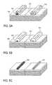
- FIGS. 5A-5Ca method as shown in FIGS. 5A-5C may be performed.
- a sacrificial film 510may be formed on the free semiconductor surfaces of bodies 206 and 207 .
- a thermal oxidationis performed to oxidize the sacrificial film and a portion of the bodies 206 and 207 , forming an oxidized region 520 .
- the oxidized region 520is selectively removed by commonly known means such as HF, leaving bodies 206 and 207 with a reduced dimension, as shown in FIG.
- the sacrificial film 510is an epitaxial semiconductor formed by commonly known techniques, as shown in FIG. 5A .
- the sacrificial filmcan be of a same or different material or composition as the bodies 206 and 207 .
- the sacrificial filmis silicon.
- the sacrificial filmis a SiGe alloy.
- the filmmay be a composite region with a buffer SiGe film and a silicon capping film.
- the dimensions of 206 and 207 after oxidationare sublithographic.
- the oxidationreduces the pre-oxidation thickness and width of semiconductor bodies 206 and 207 by about half.
- a condensationmay occur during thermal oxidation of film 510 thereby changing the final composition of the bodies 206 and 207 .
- the germanium concentration of SiGe body 206is increased by the amount of germanium present in film 510 and by the extent of the oxidation performed on the body 206 .
- body 206will have a germanium concentration resulting from the cumulative formation of alloyed region 335 and thermal oxidation of film 510
- body 207will have a germanium concentration resulting from just the thermal oxidation of the film 510
- a first pMOS device formed from body 206will have a first threshold voltage
- a second pMOS device formed from body 207will have a second threshold voltage.
- a gate dielectric layer 212is formed on each of the semiconductor bodies 206 and 207 in a manner dependent on the type of device (single-gate, dual-gate, tri-gate, etc.).
- a gate dielectric layer 212is formed on the top surface of each of the semiconductor bodies 206 and 207 , as well as on the opposite sidewalls of each of the semiconductor bodies.
- the gate dielectricis not formed on the top surface of bodies 206 and 207 .
- the gate dielectriccan be a deposited dielectric or a grown dielectric.
- the gate dielectric layer 212is a silicon dioxide dielectric film grown with a dry/wet oxidation process.
- the gate dielectric film 212is a deposited high dielectric constant (high-K) metal oxide dielectric, such as tantalum pentaoxide, titanium oxide, hafnium oxide, zirconium oxide, aluminum oxide, or another high-K dielectric, such as barium strontium titanate (BST).
- high-K metal oxide dielectricsuch as tantalum pentaoxide, titanium oxide, hafnium oxide, zirconium oxide, aluminum oxide, or another high-K dielectric, such as barium strontium titanate (BST).
- a high-K filmcan be formed by well-known techniques, such as chemical vapor deposition (CVD) and atomic layer deposition (ALD).
- a gate electrode 213is formed on both the pMOS and nMOS devices.
- the same gate electrode materialis used for both the pMOS device 204 and nMOS device 205 .
- the gate electrode 213is formed on the gate dielectric layer 212 formed on the top surface of each of semiconductor bodies 206 and 207 and is formed on the gate dielectric 212 formed on the sidewalls of each bodies 206 and 207 .
- the gate electrodecan be formed to a thickness between 200-3000 ⁇ . In an embodiment, the gate electrode has a thickness of at least three times the height of the semiconductor bodies 206 and 207 .
- the gate electrodeis a mid-gap metal gate electrode such as, tungsten, tantalum nitride, titanium nitride or titanium silicide, nickel silicide, or cobalt silicide.
- gate electrode 213is simultaneously formed for both the pMOS device 204 and nMOS device 205 by well-known techniques, such as blanket depositing a gate electrode material over the substrate of and then patterning the gate electrode material for both the pMOS and nMOS devices through photolithography and etch.
- “replacement gate” methodsare used to form both the pMOS and nMOS gate electrodes 213 , concurrently or otherwise.
- Source regions 216 and drain regions 217 for the transistorare formed in semiconductor bodies 206 and 207 on opposite sides of gate electrode 213 , as shown in FIG. 3F .
- the source and drain regionsinclude tip or source/drain extension regions.
- the semiconductor fin or body 206is doped to p-type conductivity and to a concentration between 1 ⁇ 10 19 -1 ⁇ 10 21 atoms/cm 3 .
- the semiconductor fin or body 207is doped with n-type conductivity ions to a concentration between 1 ⁇ 10 19 -1 ⁇ 10 21 atoms/cm 3 .
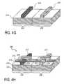
- FIGS. 4A-4HA method of fabricating a CMOS device on a bulk substrate in accordance with an embodiment of the present invention as shown in FIG. 2B is illustrated in FIGS. 4A-4H .
- the method of fabrication on a bulk substrate in accordance with an embodiment of the present inventionis relatively similar to the method of fabrication previously described for an SOI structure in reference to FIGS. 3A-3F .
- the substrate 202 of FIG. 4Ais a “bulk” semiconductor substrate, such as a silicon monocrystalline substrate or gallium arsenide substrate.
- the substrate 202is a silicon semiconductor substrate having a doped epitaxial region with either p-type or n-type conductivity having an impurity concentration level between 1 ⁇ 10 16 -1 ⁇ 10 19 atoms/cm 3 .
- the substrate 202is a silicon semiconductor substrate upon which there is an undoped, or intrinsic epitaxial silicon region.
- a well region of semiconductor substrate 202is selectively doped to p-type or n-type conductivity with a concentration level between about 1 ⁇ 10 16 -1 ⁇ 10 19 atoms/cm 3 .
- Semiconductor substrate 202can be doped by, for example, ion-implantation enabling both pMOS and NMOS well regions to be fabricated easily on the same substrate. The doping level of the semiconductor substrate 202 at this point can determine the doping level of the channel region of the device.
- a masking layer 410like masking layer 310 in FIG. 3A , is used to define the active regions of the devices 204 and 205 on the bulk semiconductor substrate.
- the method of forming masking layer 410can be essentially the same as those described for masking layer 310 of FIG. 3A .
- epitaxial semiconductor film 425is then formed on the region of substrate 202 not protected by making layer 410 , in the same manner as described in reference to FIG. 3B for the SOI substrate.
- outdiffusion barrier 430is formed in the manner described in reference to FIG. 3C .
- Film 425is intermixed with a region of semiconductor substrate 202 to form alloyed region 435 .
- the mask 420 and outdiffusion barrier 430are removed and mask 410 may be formed as described in reference to FIG. 3D .
- the semiconductor regions 435 and 202are etched using commonly known methods, very similar to those previously described for semiconductor regions 335 and 315 of SOI substrate in reference to FIG. 3E , to form recesses or trenches 440 on the substrate in alignment with the outside edges of masking portion 410 .
- the trenches 440are etched to a depth sufficient to isolate adjacent transistors from one another. In a particular embodiment, trenches 440 are etched to a depth greater than the thickness of region 435 . As shown in FIG. 4F , the trenches 440 are filled with a dielectric to form shallow trench isolation (STI) regions 210 on substrate 202 . In an embodiment of the present invention, a liner of oxide or nitride on the bottom and sidewalls of the trenches 440 is formed by commonly known methods, such as thermal oxidation and nitridation. Next, the trenches 440 are filled by blanket depositing an oxide over the liner by, for example, a high-density plasma (HDP) chemical vapor deposition process.
- HDPhigh-density plasma
- the deposition processwill also form dielectric on the top surfaces of the mask portions 410 .
- the fill dielectric layercan then be removed from the top of mask portions 410 by chemical, mechanical, or electrochemical, polishing techniques. The polishing is continued until the mask portions 410 are revealed, forming STI regions 210 . In an embodiment of the present invention, as shown in FIG. 4F , the mask portions 410 are selectively removed at this time.
- the STI regions 210are etched back or recessed to form the sidewalls of the semiconductor bodies 206 and 207 of the device 204 and complementary device 205 , respectively.
- STI regions 210are etched back with an etchant, which does not significantly etch the semiconductor bodies 206 and 207 .
- isolation regions 210can be recessed with an etchant comprising a fluorine ion, such as HF.
- STI regions 210are recessed using a commonly known anisotropic etch followed by an isotropic etch to completely remove the STI dielectric from the sidewalls of the semiconductor bodies 206 and 207 .
- STI regions 210are recessed by an amount dependent on the desired channel width of the transistors formed in 204 and 205 . In a particular embodiment, the STI regions 210 are recessed by an amount less than thickness of film 435 . In another embodiment of the present invention, STI regions 210 are recessed by approximately the same amount as the width dimension of the top surface of the semiconductor bodies 206 and 207 . In other embodiments, the STI regions 210 are recessed by a significantly larger amount than the width dimension of the top surface of the semiconductor bodies 206 and 207 . In still other embodiments, the STI regions 210 are not recessed so that planar, or single-gate, devices can be formed.
- semiconductor sacrificial regionmay also be formed on semiconductor bodies 206 and 207 and oxidized, if desired.
- a gate insulator 212 , gate electrode 213 , source regions 216 , and drain regions 217are formed on both the device in region 204 and complementary device in region 205 following embodiments analogous to those previously described in the context of an SOI substrate in reference to FIG. 3F .
- the transistors of the present invention formed on a bulk substrateis substantially complete and only device interconnection remains.
Landscapes
- Metal-Oxide And Bipolar Metal-Oxide Semiconductor Integrated Circuits (AREA)
Abstract
Description
- This application relates to the application entitled “CMOS devices with a Single Work Function Gate Electrode and Method of Fabrication,” filed on Sep. 28, 2005.
- 1. Field of the Invention
- The present invention relates to the field of semiconductor integrated circuit manufacturing, and more particularly to CMOS (complementary metal oxide semiconductor) devices having gate electrodes with a single work function.
- 2. Discussion of Related Art
- During the past two decades, the physical dimensions of MOSFETs have been aggressively scaled for low-power, high-performance CMOS applications. In order to continue scaling future generations of CMOS, the use of metal gate electrode technology is important. For example, further gate insulator scaling will require the use of dielectric materials with a higher dielectric constant than silicon dioxide. Devices utilizing such gate insulator materials demonstrate vastly better performance when paired with metal gate electrodes rather than traditional poly-silicon gate electrodes.
- Depending on the design of the transistors used in the CMOS process, the constraints placed on the metal gate material are somewhat different. For a planar, bulk or partially depleted, single-gate transistor, short-channel effects (SCEs) are typically controlled through channel dopant engineering. Requirements on the transistor threshold voltages then dictate the gate work-function values must be close to the conduction and valence bands of silicon. For such devices, a “mid-gap” work function gate electrode that is located in the middle of the p and n channel work function range is inadequate. A mid-gap gate electrode typically results in a transistor having either a threshold voltage that is too high for high-performance applications, or compromised SCEs when the effective channel doping is reduced to lower the threshold voltage. For non-planar or multi-gate transistor designs, the device geometry better controls SCEs and the channel may then be more lightly doped and potentially fully depleted at zero gate bias. For such devices, the threshold voltage can be determined primarily by the gate metal work function. However, even with the multi-gate transistor's improved SCEs, it is typically necessary to have a gate electrode work function about 250 meV below mid-gap for an nMOS transistor and about 250 meV above mid-gap for a pMOS transistor. Therefore, a single mid-gap gate material is also incapable of achieving low threshold voltages for both pMOS (a MOSFET with a p-channel) and nMOS (a MOSFET with an n-channel) multi-gate transistors.
- For these reasons, CMOS devices generally utilize two different gate electrodes, an nMOS electrode and a pMOS electrode, having two different work function values. For the traditional polysilicon gate electrode, the work function values are typically about 4.2 and 5.2 electron volts for the nMOS and pMOS electrodes respectively, and they are generally formed by doping the polysilicon material to be either n or p type. Attempts at changing the work function of metal gate materials to achieve similar threshold voltages is difficult as the metal work function must either be varied with an alloy mixture or two different metals utilized for n and p-channel devices.
- One such
conventional CMOS device 100 is shown inFIG. 1 , where insulating substrate102, having acarrier 101 and aninsulator 103, has a pMOS transistor region104 and anNMOS transistor region 105. The pMOS device104 is comprised of anon-planar semiconductor body 106 having asource 116 and adrain 117, agate insulator 112 and agate electrode 113 made of a “p-metal” (a metal having a work function appropriate for a low pMOS transistor threshold voltage). The nMOSdevice 105 is comprised of anon-planar semiconductor body 107 having asource 116 and adrain 117, agate insulator 112 and agate electrode 114 made of an “n-metal” (a metal having a work function appropriate for a low nMOS transistor threshold voltage). While fabricating transistors having gate electrodes made of two different materials is prohibitively expensive, simpler approaches to dual-metal gate integration like work-function engineering of the metal film suffer from problems such as poor reliability and insufficient work-function shift. FIG. 1 is an illustration of a perspective view of conventional non-planar transistors on an insulating substrate and conventional gate electrodes.FIG. 2A is an illustration of a perspective view of non-planar transistors on an insulating substrate and gate electrodes in accordance with the present invention.FIG. 2B is an illustration of a perspective view of non-planar transistors on a bulk substrate and gate electrodes in accordance with the present invention.FIGS. 3A-3F are illustrations of perspective views of non-planar transistors on an insulating substrate with gate electrodes in accordance with the present invention.FIGS. 4A-4H are illustrations of perspective views of non-planar transistors on a bulk substrate with gate electrodes in accordance with the present invention.FIGS. 5A-5C are illustrations of perspective views of a method of fabricating non-planar bodies for transistors in accordance with the present invention.- A novel device structure and its method of fabrication are described. In the following description, numerous specific details are set forth, such as specific materials, dimensions and processes, etc. in order to provide a thorough understanding of the present invention. In other instances, well-known semiconductor processes and manufacturing techniques have not been described in particular detail in order to not unnecessarily obscure the present invention.
- Embodiments of the present invention include complementary (pMOS and nMOS) transistors having semiconductor channel regions which have been band gap engineered to achieve a low threshold voltage. In particular embodiments, the complementary devices utilize the same material having a single work function as the gate electrode. Engineering the band gap of the semiconductor transistor channels rather than engineering the work function of the transistor gate metal for the individual pMOS and nMOS devices avoids the manufacturing difficulties associated with depositing and interconnecting two separate gate metals in a dual-metal gate process. A single metal gate stack, used for both pMOS and nMOS transistors, simplifies fabrication while engineering the band gap of the semiconductor transistor channels enables independent tuning of the pMOS and nMOS threshold voltages. In embodiments of the present invention, the threshold voltage of a device can be targeted through the use of semiconductor materials that have an appropriate valance band (nMOS) or conduction band (pMOS) offset relative to the substrate. Therefore, embodiments of the present invention can utilize a single mid-band gap metal for both the pMOS and nMOS transistors in a CMOS device while still achieving a low threshold voltage for both the pMOS and nMOS transistors.
- An example of a
CMOS device 200 with a metal gate structure and an engineered band gap in accordance with an embodiment of the present invention is illustrated inFIG. 2A . AlthoughFIG. 2A shows a tri-gate embodiment of the present invention, it should be appreciated that additional embodiments comprising single-gate or multi-gate transistors (such as dual-gate, FinFET, omega-gate) designs are also possible.CMOS device 200 comprises a transistor of a first conductivity type on afirst region 204 and a transistor of a complementary conductivity type on asecond region 205 ofsubstrate 202. In embodiments of the present invention, as depicted in bothFIGS. 2A and 2B , at least a portion of thesemiconductor body 206 is formed on a region of the semiconductor substrate that has been alloyed with an epitaxial film and thus has a narrower band gap than thesemiconductor body 207. The narrow band gap semiconductor alloy will then reduce the effective threshold voltage of a pMOS transistor inregion 204 by an amount approximately equal to the conduction band offset between the semiconductor alloy used forbody 206 and anon-alloyed semiconductor body 207 inregion 205. Similarly, in other embodiments, a valence band offset between the alloyed semiconductor material oftransistor body 206 and the unalloyed semiconductor material oftransistor body 207 modifies the effective threshold voltage of an nMOS transistor. In a further embodiment, a semiconductor body having a larger band gap can be used to increase either a pMOS or an nMOS transistor's threshold voltage by the respective band offset relative to the unalloyed substrate on which the transistors are formed in order to reduce transistor leakage or increase a transistor's breakdown voltage. - In alternate embodiments of the present invention (not shown) both the pMOS transistor and nMOS transistor channels are formed on an alloyed semiconductor substrate material. When both alloyed semiconductor regions have only a conduction band offset (no valence band offset) relative to the unalloyed substrate regions, the band gap engineered alloyed semiconductor region of the nMOS transistor will not have any effect on the nMOS threshold voltage.
- In a particular embodiment of the present invention, as shown in
FIG. 2A ,CMOS device 200 includes non-planarmonocrystalline semiconductor bodies insulating layer 203 overcarrier 201. In certain embodiments of the present invention,bodies insulator 203 over acarrier 201.Semiconductor bodies insulator 203, the structure is commonly referred to as silicon/semiconductor-on-insulator, or SOI, substrate. In an embodiment of the present invention, the semiconductor film oninsulator 203 is comprised of a monocrystalline silicon semiconductor doped with either p-type or n-type conductivity with a concentration level between 1×10¹⁶-1×10¹⁹atoms/cm3. In another embodiment of the present invention, the semiconductor film formed oninsulator 203 is comprised of a silicon semiconductor substrate having an undoped, or intrinsic epitaxial silicon region.Insulator 203 can be any dielectric material andcarrier 201 can be any well-known semiconductor, insulator or metallic material. - In another embodiment of the invention, as shown in
device 300 ofFIG. 2B , a “bulk” substrate is used andsemiconductor bodies substrate 202 is comprised of a silicon semiconductor substrate having a doped epitaxial silicon region with either p-type or n-type conductivity with a concentration level between 1×10¹⁶-1×10¹⁹atoms/cm3. In another embodiment of the present invention, thesubstrate 202 is comprised of a silicon semiconductor substrate having an undoped, or intrinsic epitaxial silicon region. In bulk substrate embodiments of the present invention,isolation regions 210 are formed on the bulk, monocrystalline, semiconductor and border thesemiconductor bodies FIG. 2B . In some embodiments, at least a portion of the sidewalls of thebodies isolation regions 210. In other embodiments, such as for planar single-gate designs, thesemiconductor bodies - In the embodiments shown in
FIGS. 2A and 2B ,semiconductor bodies semiconductor bodies semiconductor bodies FIG. 2A . In embodiments with a bulk substrate,semiconductor bodies isolation region 210 bordering the body, as shown inFIG. 2B . The distance between the top surface and the bottom surface defines an individual semiconductor body height. In an embodiment of the present invention, the individual body height is substantially equal to the individual semiconductor body width. In a particular embodiment of the present invention, thesemiconductor bodies - In an embodiment of the present CMOS invention, the
alloyed semiconductor body 206 is single crystalline to ensure sufficient carrier lifetime and mobility.Semiconductor body 206 can be formed of any well-known semiconductor material, such as silicon germanium (SiGe), silicon carbide (SiC), indium gallium arsenide (InxGa1-xAsy), indium antimonide (InxSby), indium gallium phosphide (InxGa1-xPy), or carbon nanotubes (CNT). In certain embodiments of the present invention, thesemiconductor body 206 is an alloy of silicon and germanium (SiGe). In certain other embodiments, one semiconductor body is an alloy of silicon and carbon (SiC). - Embodiments of the present invention include decreasing the conduction band energy of a pMOS transistor having a SiGe channel region by increasing the concentration of the germanium. In this manner, it is possible to fabricate both a pMOS and nMOS multi-gate transistor having gate electrodes of the same material and threshold voltage magnitudes less than 0.7 V over a range of transistor channel doping levels. As the conduction band energy decreases, the threshold voltage is lowered by an amount approximately equal to the conduction band voltage offset. In an embodiment of the present invention, the germanium concentration of the alloyed region is between 5 and 50 percent, and more particularly, between 15 and 30 percent. For embodiments having about 25 percent germanium, the conduction band energy is decreased by about 300 meV below the conduction band of silicon. Thus, a pMOS device having a SiGe channel region comprised of about 25 percent germanium will have a threshold voltage magnitude approximately 300 meV less than that of a pure silicon channel.
- In embodiments of the present invention, nMOS multi-gate devices have a work function difference (the difference between the gate metal work function an the semiconductor work function or (φmetal-φsemiconductor) of about 0.4 eV while the work function difference for a pMOS multi-gate device is about 0.7 eV. In a particular embodiment of the present invention, the 0.4 eV nMOS work function difference is achieved through Fermi-level pinning a mid-gap titanium nitride metal gate material (having a work function of about 4.7 eV). In a further embodiment of the present invention, a 0.7 eV pMOS work function difference is achieved with a band-engineered SiGe channel region comprised of about 25 percent germanium. The 25 percent germanium decreases the channel semiconductor conduction band energy and, in effect, shifts the work function difference of the mid-gap titanium nitride metal gate material by about 300 mV, from the pinned Fermi-level of 0.4 eV to the desired 0.7 eV.
- Embodiments of the present invention include adjusting the germanium concentration of a pMOS SiGe body to adjust the threshold voltage, enabling multiple threshold voltages on the same chip, which is a different challenge from setting a single threshold voltage to match an nMOS device. For ULSI systems, it is typically necessary to provide a menu of devices with different threshold voltages to allow for the optimization of performance and power consumption. The ability to tune the threshold voltage by about 150 mV is often required. For devices with geometries in the sub-50-nm gate-length regime, it is very difficult to achieve such a range by merely doping the transistor channel. Disadvantageous channel doping can by avoided by embodiments of the present invention where a first pMOS device has a channel comprised of a first germanium concentration targeting a first threshold voltage while a second pMOS device has a channel comprised of a second germanium concentration targeting a second threshold voltage.
- As shown in
FIGS. 2A and 2B ,CMOS devices gate insulator layer 212. In the depicted embodiments,gate insulator 212 surrounds thesemiconductor bodies gate dielectric layer 212 is formed on the sidewalls as well as on the top surfaces of thesemiconductor bodies FIGS. 2A and 2B . In other embodiments, such as in FinFET or dual-gate designs,gate dielectric layer 212 is only formed on the sidewalls of thesemiconductor bodies Gate insulator 212 can be of any commonly known dielectric material compatible with the semiconductor bodies and thegate electrode 213. In an embodiment of the present invention, the gate dielectric layer is a silicon dioxide (SiO2), silicon oxynitride (SiOxNy) or a silicon nitride (Si3N4) dielectric layer. In one particular embodiment of the present invention, thegate dielectric layer 212 is a silicon oxynitride film formed to a thickness of between 5-20 Å. In another embodiment of the present invention,gate dielectric layer 212 is a high K gate dielectric layer, such as a metal oxide dielectric, such as to tantalum oxide, titanium oxide, hafnium oxide, zirconium oxide, or aluminum oxide.Gate dielectric layer 212 can also be other types of high K dielectric, such as lead zirconium titanate (PZT). CMOS devices gate electrode 213, as shown inFIGS. 2A and 2B , respectively. In certain embodiments,gate electrode 213 is formed ongate dielectric layer 212 over the sidewalls of each of thesemiconductor bodies Gate electrode 213 has a pair of laterally opposite sidewalls separated by a distance, defining the gate length (Lg) of transistors inregion regions FIGS. 2A and 2B , the same material is used to form thegate electrode 213 for pMOS device inregion 204 and nMOS device inregion 205. In this manner, CMOS device fabrication can be greatly simplified because there is no need for the pMOS device to have a gate metal with a different work function than that of the nMOS device. In further embodiments of the present invention, the same gate electrode structure physically connects a pMOS device to an nMOS device.Gate electrode 213 ofFIGS. 2A and 2B can be formed of any suitable gate electrode material having the appropriate work function. In an embodiment of the present invention, the gate electrode is a metal gate electrode, such as tungsten, tantalum nitride, titanium nitride or titanium silicide, nickel silicide, or cobalt silicide. In an embodiment of the present invention, thegate electrode 213 of both the pMOS device and then nMOS device is formed from a material having a mid-gap work function between 4.5 and 4.9 eV. In a specific embodiment of the present invention,gate electrode 213 comprises titanium nitride having a work function equal to about 4.7 eV. It should also be appreciated that thegate electrode 213 need not necessarily be a single material, but rather can also be a composite stack of thin films such as a metal/polycrystalline silicon electrode.- As shown in
FIGS. 2A and 2B , a pair ofsource 216 and drain217 regions are formed inbody 206 andbody 207 on opposite sides ofgate electrode 213. Thesource region 216 and thedrain region 217 are formed of the same conductivity type such as n-type or p-type conductivity, depending on if the transistor is an nMOS device or a pMOS device. In an embodiment of the present invention,source region 216 and drainregion 217 have a doping concentration of 1×10¹⁹-1×10²¹atoms/cm3.Source region 216 and drainregion 217 can be formed of uniform concentration or can include subregions of different concentrations or doping profiles such as tip regions (e.g., source/drain extensions). - As shown in
FIGS. 2A and 2B , the channel region of the pMOS and nMOS devices is the portion ofsemiconductor bodies source regions 216 anddrain regions 217 under thegate insulator 212 andgate electrode 213. In certain embodiments of the present invention, a pMOS device formed inregion 204 has a channel region of undoped SiGe. In other embodiments the channel regions ofbody 206 andbody 207 are doped SiGe. In an embodiment of the present invention, the channel region ofsemiconductor body 207 is intrinsic or undoped silicon. In another embodiment of the present invention, channel region ofsemiconductor body 207 is doped silicon. When the channel region is doped, it is typically doped to the opposite conductivity type of thesource region 216 and thedrain region 217. For example, thenMOS device 205 has source and drain regions which are n-type conductivity while the channel region is doped to p-type conductivity. When channel region is doped, it can be doped to a conductivity level of between 1×10¹⁶to 1×10¹⁹atoms/cm3. In certain multi-gate transistor embodiments of the present invention, the pMOS channel regions have an impurity concentration of 1017to 10e18atoms/cm3. - A method of fabricating a CMOS device on an insulating substrate in accordance with an embodiment of the present invention as shown in
FIG. 2A is illustrated inFIGS. 3A-3F . Insulating substrate can be formed in any commonly known fashion. In an embodiment of the present invention, shown inFIG. 3A , the insulating substrate includes a lowermonocrystalline silicon carrier 201 upon which there is aninsulating layer 203, such as a silicon dioxide film or silicon nitride film. Insulatinglayer 203 isolatessemiconductor film 315 fromcarrier 201, and in an embodiment is formed to a thickness between 200-2000 Å. Insulatinglayer 203 is sometimes referred to as a “buried oxide” layer and the substrate comprised of201,203 and315 is referred to as a silicon or semiconductor on insulating (SOI) substrate. - Although the
semiconductor film 315 is ideally a silicon film, in other embodiments it can be other types of semiconductor films, such as germanium (Ge), a silicon germanium alloy (SiGe), gallium arsenide (GaAs), InSb, GaP, GaSb, or InP. In an embodiment of the present invention,semiconductor film 315 is an intrinsic (i.e., undoped) silicon film. In other embodiments,semiconductor film 315 is doped to p-type or n-type conductivity with a concentration level between 1×10¹⁶-1×10¹⁹atoms/cm3.Semiconductor film 315 can be in-situ doped (i.e., doped while it is deposited) or doped after it is formed onsubstrate 202 by for example ion-implantation. Doping after formation enablescomplementary devices semiconductor substrate film 315 at this point can determine the doping level of the channel region of the device. - In certain embodiments of the present invention,
semiconductor substrate film 315 is formed to a thickness approximately equal to the height desired for the subsequently formed semiconductor body or bodies of the fabricated transistor. In an embodiment of the present invention,semiconductor substrate film 315 has a thickness or height of less than 30 nanometers and ideally less than 20 nanometers. In certain embodiments of the present invention,semiconductor substrate region 315 is formed to a thickness enabling the fabricated transistor to be operated in a fully depleted manner for its designed gate length (Lg). Semiconductor substrate region 315 can be formed oninsulator 203 in any well-known method. In one method of forming a silicon-on-insulator substrate, known as the separation by implantation of oxygen (SIMOX) technique. Another technique currently used to form SOI substrates is an epitaxial silicon film transfer technique generally referred to as bonded SOI.- If desired, a masking can be formed over any regions of the substrate where there is to be no epitaxial semiconductor region subsequently formed on
substrate region 315. In a particular embodiment shown inFIG. 3A ,mask layer 320 is formed over theregion 205.Mask layer 320 can be of any commonly known material capable of surviving the subsequent process of forming the epitaxial semiconductor region. In an embodiment of the present invention,mask layer 320 is a dielectric material capable of serving as a good diffusion barrier, such as silicon nitride. As shown inFIG. 3A , a pad oxide is typically used as a buffer layer between the silicon nitride mask andsemiconductor substrate region 315. Commonly known techniques, such as CVD, LPCVD, or PECVD may be used to deposit the mask material.Mask 320 is then selectively defined by commonly known lithography and etch techniques, so that themask 320 is substantially removed from theregion 204. In certain embodiments of the present invention, when theepitaxial semiconductor film 325 is to be formed on all transistors, nomask layer 320 is formed. - An
epitaxial semiconductor film 325 is then formed onsubstrate film 315. In certain embodiments,epitaxial semiconductor film 325 is selectively formed on thesubstrate region 204 where a pMOS device is desired, as shown inFIG. 3B . Any commonly known epitaxial processes suitable for the particular semiconductor materials can be used to form thesemiconductor film 325. In a particular embodiment, an LPCVD process using germane and a silicon source gas, such as a silane, as precursors forms aSiGe film 325 onsilicon semiconductor region 315. In a further embodiment, HCl can be utilized during the SiGe growth to improve the selectivity of the growth. Another embodiment comprises asilicon film 325 grown on aSiGe film 315. In yet another embodiment a silicon-carbide film 325 is formed on asilicon film 315. In still another embodiment asilicon film 325 is formed on a silicon-carbide film 315.Film 325 can be grown to have a particular composition determined by the final amount of band offset desired for the transistor. In a particular embodiment of the present invention a silicon-germanium film 325 having about 5 percent to about 30 percent germanium is formed. In other embodiments, the germanium concentration is 50 percent, or more. Ideally, the formation process is capable of producing a singlecrystalline semiconductor film 325 from the surface ofsemiconductor substrate film 315. Thesemiconductor film 325 is grown to the desired thickness, some embodiments including in-situ impurity doping. In certain embodiments where thesemiconductor film 325 is not lattice matched to thesubstrate semiconductor film 315, the maximum thickness is the critical thickness. - Subsequent to the formation of the
epitaxial semiconductor film 325, anoutdiffusion barrier 330 is formed overfilm 325. Theoutdiffusion barrier 330 can be formed from any commonly known material capable of limiting the loss of constituents from theepitaxial semiconductor film 325 during subsequent elevated-temperature processes. While, theoutdiffusion barrier 330 need not be directly on or in intimate contact withepitaxial semiconductor film 325, in the particular embodiment shown inFIG. 3C , a thermally grownoxide 330 of thefilm 325 forms the outdiffusion barrier. In other embodiments, theoutdiffusion barrier 330 is formed from a deposited dielectric such as a silicon dioxide, or nitride. In particular embodiments where thefilm 325 is SiGe having a relatively high germanium concentration, above about 20 percent, the quality of the oxides formed onepitaxial semiconductor film 325 degrades and it becomes more difficult to form a film capable of preventing outdiffusion of germanium. Therefore, in some embodiments of the present invention, theoutdiffusion barrier 330 is formed from a high-k dielectric material. The high-k dielectric material used foroutdiffusion barrier 330 may be of any commonly known material, such as a metal oxide dielectric, such as to tantalum oxide, titanium oxide, hafnium oxide, zirconium oxide, or aluminum oxide. The high-K film can be formed by well-known techniques, such as chemical vapor deposition (CVD) and atomic layer deposition (ALD). - Next, an elevated-temperature anneal is performed to intermix the constituents of
epitaxial film 325 andsubstrate film 315 into asemiconductor alloy region 335 having the desired band gap and band offsets. In a particular embodiment, the anneal is performed by commonly known techniques, such as rapid thermal anneal (RTP) or furnace anneal, for a time sufficient to uniformly distribute the constituents offilm 325 andsubstrate film 315.Region 335, shown inFIG. 3C , is a single crystal semiconductor having excellent film quality and electronic properties consistent with the alloy formed fromepitaxial semiconductor film 325 andsubstrate film 315.Substrate region 335 then has the desired band gap and offset necessary to provide the desired threshold voltage of the device formed onregion 335. In specific embodiments where theoutdiffusion barrier 330 is a thermal oxide offilm 325, the outdiffusion barrier thickness increases asfilm 325 is oxidized. Constituents offilm 325 oxidized less readily are pushed from the oxidizedregion 330 to the unoxidized portion offilm 325 andunderlying substrate film 315. This phenomenon is commonly referred to as condensation. In a particular embodiment of the present invention wherefilm 325 is SiGe andsubstrate film 315 is silicon, the silicon atoms of325 oxidize more readily than germanium atoms. Because oxide layers330 and203 block germanium from diffusion out offilms alloyed SiGe region 335 is increased up to the ratio of the thickness ofepitaxial semiconductor film 325 to that ofregion 335 multiplied by the initial germanium concentration ofepitaxial film 325. In this particular embodiment, a highgermanium concentration region 335 can be formed fromsilicon substrate film 315 to produce a SiGe on an insulator (SGOI) region locally, only where a particular device is to be formed, rather than forming SiGe globally, across the entire substrate. - In a particular embodiment where
epitaxial film 325 is SiGe andbarrier 330 is a thermal oxide, the anneal is performed for a duration sufficient to completely oxidize theepitaxial film 325, such that theinitial substrate film 315 in alloyedform 335 is the only semiconductor region aboveinsulator 203. In a more particular embodiment,film 315 is about 20 nanometers thick with a germanium concentration of about 25 percent after the alloying anneal. In other embodiments wherefilm 325 is SiGe and theoutdiffusion barrier 330 is a deposited dielectric, no condensation occurs and the constituents ofsubstrate film 315 andepitaxial film 325 merely interdiffuse, or intermix, and the final thickness of thesemiconductor film 335 is the sum of the thickness ofsubstrate film 315 and that offilm 325. In certain embodiments of the present invention, various regions offilm 325 are selectively masked with an outdiffusion barrier havingcharacteristics enabling film 325 to have different alloy compositions and therefore different band offsets after intermixing. In these embodiments, devices with various voltage threshold characteristics can be achieved on the same substrate. In one such embodiment, anoutdiffusion barrier 330 is formed from a deposited oxide, patterned with commonly known methods, and athermal outdiffusion barrier 330 then formed on the regions offilm 325 not covered by the deposited outdiffusion barrier. After intermixing,region 335 formed in areas wherefilm 325 was covered with the deposited oxide would have a different alloy concentration thanregion 335 formed in areas wherefilm 325 was covered with a thermal oxide and thus, transistors formed in the different alloy regions would have different threshold voltages. - Wells can then be selectively formed for pMOS and nMOS transistors using any commonly known technique to dope regions to a desired impurity concentration. In a certain embodiment of the present invention,
outdiffusion barrier 330 andmask 320 are selectively removed fromregions outdiffusion barrier 330 andmask 320 are removed and commonly known lithography used to selectively form well regions. In embodiments of the present invention,regions alloy region 335 has a valence band offset of about 300 mV and an n-type channel impurity concentration level of about 1×10¹⁷-1×10¹⁸atoms/cm3. - Once
films masking layer 310 can be used to define the active regions of the devices in alloyedsemiconductor region 335 andnon-alloyed semiconductor region 315. Themasking layer 310 can be any well-known material suitable for defining thesemiconductors layer 310 is a lithographically defined photo resist. In other embodiments,mask 310 is formed of a dielectric material that has been lithographically defined and then etched using commonly known techniques. In the particular embodiment shown inFIG. 3D , masking layer can be a composite stack of materials, such as an oxide/nitride stack. As shown inFIG. 3E , once maskinglayer 310 has been defined,semiconductor regions semiconductor bodies semiconductor bodies body 206 is a SiGe alloy andbody 207 is silicon, a commonly known plasma etch can be used to delineate bothbody 206 andbody 207 followed by wet etches known in the art to be appropriate for the germanium composition ofbody 206 and for silicon ofbody 207. For planar, or single-gate embodiments, the planar devices are merely formed on thefilms mask 310 is used to define isolation regions. In a further embodiment, as shown inFIG. 3E , maskinglayer 310 is removed from thesemiconductor bodies layer 310. In other embodiments, such as for particular dual-gate or FinFET designs, maskinglayer 310 is not removed, so thatlayer 310 can subsequently provide isolation from thegate electrode 213. - Once the
semiconductor bodies FIGS. 5A-5C may be performed. As shown inFIG. 5A , asacrificial film 510 may be formed on the free semiconductor surfaces ofbodies sacrificial film 510, a thermal oxidation is performed to oxidize the sacrificial film and a portion of thebodies oxidized region 520. Following the oxidation, the oxidizedregion 520 is selectively removed by commonly known means such as HF, leavingbodies FIG. 5C . The oxidation reduces the dimensions ofsemiconductor bodies sacrificial film 510 improves the smoothness and reduces the defect states of thebodies bodies sacrificial film 510 is an epitaxial semiconductor formed by commonly known techniques, as shown inFIG. 5A . The sacrificial film can be of a same or different material or composition as thebodies semiconductor bodies sacrificial film 510, a condensation may occur during thermal oxidation offilm 510 thereby changing the final composition of thebodies SiGe body 206 is increased by the amount of germanium present infilm 510 and by the extent of the oxidation performed on thebody 206. In certain embodiments,body 206 will have a germanium concentration resulting from the cumulative formation of alloyedregion 335 and thermal oxidation offilm 510, whilebody 207 will have a germanium concentration resulting from just the thermal oxidation of thefilm 510. In a further embodiment, a first pMOS device formed frombody 206 will have a first threshold voltage and a second pMOS device formed frombody 207 will have a second threshold voltage. - Once the
bodies gate dielectric layer 212, as shown inFIG. 3F , is formed on each of thesemiconductor bodies gate dielectric layer 212 is formed on the top surface of each of thesemiconductor bodies bodies gate dielectric layer 212 is a silicon dioxide dielectric film grown with a dry/wet oxidation process. In an embodiment of the present invention, thegate dielectric film 212 is a deposited high dielectric constant (high-K) metal oxide dielectric, such as tantalum pentaoxide, titanium oxide, hafnium oxide, zirconium oxide, aluminum oxide, or another high-K dielectric, such as barium strontium titanate (BST). A high-K film can be formed by well-known techniques, such as chemical vapor deposition (CVD) and atomic layer deposition (ALD). - As shown in
FIG. 3F , agate electrode 213 is formed on both the pMOS and nMOS devices. In certain embodiments, the same gate electrode material is used for both thepMOS device 204 andnMOS device 205. In an embodiment of the present invention, thegate electrode 213 is formed on thegate dielectric layer 212 formed on the top surface of each ofsemiconductor bodies gate dielectric 212 formed on the sidewalls of eachbodies semiconductor bodies invention gate electrode 213 is simultaneously formed for both thepMOS device 204 andnMOS device 205 by well-known techniques, such as blanket depositing a gate electrode material over the substrate of and then patterning the gate electrode material for both the pMOS and nMOS devices through photolithography and etch. In other embodiments of the present invention, “replacement gate” methods are used to form both the pMOS andnMOS gate electrodes 213, concurrently or otherwise. Source regions 216 anddrain regions 217 for the transistor are formed insemiconductor bodies gate electrode 213, as shown inFIG. 3F . In an embodiment of the present invention, the source and drain regions include tip or source/drain extension regions. For a pMOS transistor, the semiconductor fin orbody 206 is doped to p-type conductivity and to a concentration between 1×10¹⁹-1×10²¹atoms/cm3. For an nMOS transistor, the semiconductor fin orbody 207 is doped with n-type conductivity ions to a concentration between 1×10¹⁹-1×10²¹atoms/cm3. At this point the CMOS device of the present invention is substantially complete and only device interconnection remains.- A method of fabricating a CMOS device on a bulk substrate in accordance with an embodiment of the present invention as shown in
FIG. 2B is illustrated inFIGS. 4A-4H . The method of fabrication on a bulk substrate in accordance with an embodiment of the present invention is relatively similar to the method of fabrication previously described for an SOI structure in reference toFIGS. 3A-3F . In certain embodiments of the present invention, thesubstrate 202 ofFIG. 4A is a “bulk” semiconductor substrate, such as a silicon monocrystalline substrate or gallium arsenide substrate. In particular embodiments of the present invention, thesubstrate 202 is a silicon semiconductor substrate having a doped epitaxial region with either p-type or n-type conductivity having an impurity concentration level between 1×10¹⁶-1×10¹⁹atoms/cm3. In another embodiment of the present invention, thesubstrate 202 is a silicon semiconductor substrate upon which there is an undoped, or intrinsic epitaxial silicon region. - In embodiments of the present invention, a well region of
semiconductor substrate 202 is selectively doped to p-type or n-type conductivity with a concentration level between about 1×10¹⁶-1×10¹⁹atoms/cm3.Semiconductor substrate 202 can be doped by, for example, ion-implantation enabling both pMOS and NMOS well regions to be fabricated easily on the same substrate. The doping level of thesemiconductor substrate 202 at this point can determine the doping level of the channel region of the device. - As shown in
FIG. 4A , amasking layer 410, like maskinglayer 310 inFIG. 3A , is used to define the active regions of thedevices masking layer 410 can be essentially the same as those described for maskinglayer 310 ofFIG. 3A . Similarly, as shown inFIG. 3B ,epitaxial semiconductor film 425 is then formed on the region ofsubstrate 202 not protected by makinglayer 410, in the same manner as described in reference toFIG. 3B for the SOI substrate. - As shown in
FIG. 4C ,outdiffusion barrier 430 is formed in the manner described in reference toFIG. 3C .Film 425 is intermixed with a region ofsemiconductor substrate 202 to form alloyedregion 435. Following intermixing, in the embodiment shown inFIG. 4D , themask 420 andoutdiffusion barrier 430 are removed andmask 410 may be formed as described in reference toFIG. 3D . In the embodiment shown inFIG. 4E , thesemiconductor regions semiconductor regions FIG. 3E , to form recesses ortrenches 440 on the substrate in alignment with the outside edges of maskingportion 410. Thetrenches 440 are etched to a depth sufficient to isolate adjacent transistors from one another. In a particular embodiment,trenches 440 are etched to a depth greater than the thickness ofregion 435. As shown inFIG. 4F , thetrenches 440 are filled with a dielectric to form shallow trench isolation (STI)regions 210 onsubstrate 202. In an embodiment of the present invention, a liner of oxide or nitride on the bottom and sidewalls of thetrenches 440 is formed by commonly known methods, such as thermal oxidation and nitridation. Next, thetrenches 440 are filled by blanket depositing an oxide over the liner by, for example, a high-density plasma (HDP) chemical vapor deposition process. The deposition process will also form dielectric on the top surfaces of themask portions 410. The fill dielectric layer can then be removed from the top ofmask portions 410 by chemical, mechanical, or electrochemical, polishing techniques. The polishing is continued until themask portions 410 are revealed, formingSTI regions 210. In an embodiment of the present invention, as shown inFIG. 4F , themask portions 410 are selectively removed at this time. - In certain embodiments, as shown in
FIG. 4G , theSTI regions 210 are etched back or recessed to form the sidewalls of thesemiconductor bodies device 204 andcomplementary device 205, respectively.STI regions 210 are etched back with an etchant, which does not significantly etch thesemiconductor bodies isolation regions 210 can be recessed with an etchant comprising a fluorine ion, such as HF. In other embodiments,STI regions 210 are recessed using a commonly known anisotropic etch followed by an isotropic etch to completely remove the STI dielectric from the sidewalls of thesemiconductor bodies STI regions 210 are recessed by an amount dependent on the desired channel width of the transistors formed in204 and205. In a particular embodiment, theSTI regions 210 are recessed by an amount less than thickness offilm 435. In another embodiment of the present invention,STI regions 210 are recessed by approximately the same amount as the width dimension of the top surface of thesemiconductor bodies STI regions 210 are recessed by a significantly larger amount than the width dimension of the top surface of thesemiconductor bodies STI regions 210 are not recessed so that planar, or single-gate, devices can be formed. - Once the
non-planar semiconductor bodies FIGS. 5A-5C , semiconductor sacrificial region may also be formed onsemiconductor bodies FIG. 4H , agate insulator 212,gate electrode 213,source regions 216, and drainregions 217 are formed on both the device inregion 204 and complementary device inregion 205 following embodiments analogous to those previously described in the context of an SOI substrate in reference toFIG. 3F . At this point the transistors of the present invention formed on a bulk substrate is substantially complete and only device interconnection remains. - Although the invention has been described in language specific to structural features and/or methodological acts, it is to be understood that the invention defined in the appended claims is not necessarily limited to the specific features or acts described. Rather, the specific features and acts are disclosed as particularly graceful forms of implementing the claimed invention.
Claims (24)
Priority Applications (1)
| Application Number | Priority Date | Filing Date | Title |
|---|---|---|---|
| US11/238,445US20070069302A1 (en) | 2005-09-28 | 2005-09-28 | Method of fabricating CMOS devices having a single work function gate electrode by band gap engineering and article made thereby |
Applications Claiming Priority (1)
| Application Number | Priority Date | Filing Date | Title |
|---|---|---|---|
| US11/238,445US20070069302A1 (en) | 2005-09-28 | 2005-09-28 | Method of fabricating CMOS devices having a single work function gate electrode by band gap engineering and article made thereby |
Publications (1)
| Publication Number | Publication Date |
|---|---|
| US20070069302A1true US20070069302A1 (en) | 2007-03-29 |
Family
ID=37892816
Family Applications (1)
| Application Number | Title | Priority Date | Filing Date |
|---|---|---|---|
| US11/238,445AbandonedUS20070069302A1 (en) | 2005-09-28 | 2005-09-28 | Method of fabricating CMOS devices having a single work function gate electrode by band gap engineering and article made thereby |
Country Status (1)
| Country | Link |
|---|---|
| US (1) | US20070069302A1 (en) |
Cited By (32)
| Publication number | Priority date | Publication date | Assignee | Title |
|---|---|---|---|---|
| US20070111419A1 (en)* | 2005-09-28 | 2007-05-17 | Doyle Brian S | CMOS Devices with a single work function gate electrode and method of fabrication |
| US20070138565A1 (en)* | 2005-12-15 | 2007-06-21 | Intel Corporation | Extreme high mobility CMOS logic |
| US20070221956A1 (en)* | 2006-03-23 | 2007-09-27 | Kabushiki Kaisha Toshiba | Semiconductor device and method of fabricating the same |
| US20080032478A1 (en)* | 2006-08-02 | 2008-02-07 | Hudait Mantu K | Stacking fault and twin blocking barrier for integrating III-V on Si |
| US20080149984A1 (en)* | 2006-12-22 | 2008-06-26 | Chang Peter L D | Floating body memory cell having gates favoring different conductivity type regions |
| EP1993136A1 (en)* | 2007-05-14 | 2008-11-19 | Interuniversitair Microelektronica Centrum (IMEC) | Multi-gate MOSFET device and method of manufacturing same |
| US20080303095A1 (en)* | 2007-06-07 | 2008-12-11 | Weize Xiong | Varying mugfet width to adjust device characteristics |
| US20090174010A1 (en)* | 2008-01-03 | 2009-07-09 | International Business Machines Corporation | Sram device structure including same band gap transistors having gate stacks with high-k dielectrics and same work function |
| US20090315114A1 (en)* | 2008-06-23 | 2009-12-24 | Intel Corporation | Stress in trigate devices using complimentary gate fill materials |
| US20100129968A1 (en)* | 2005-11-15 | 2010-05-27 | Hong-Jyh Li | Semiconductor Devices and Methods of Manufacture Thereof |
| US20100200937A1 (en)* | 2009-02-09 | 2010-08-12 | International Business Machines Corporation | METHOD AND STRUCTURE FOR PMOS DEVICES WITH HIGH K METAL GATE INTEGRATION AND SiGe CHANNEL ENGINEERING |
| US20110031552A1 (en)* | 2009-08-07 | 2011-02-10 | Renesas Electronics Corporation | Semiconductor device and manufacturing method thereof |
| US20110068407A1 (en)* | 2009-09-24 | 2011-03-24 | Taiwan Semiconductor Manufacturing Company, Ltd. | Germanium FinFETs with Metal Gates and Stressors |
| US7989280B2 (en) | 2005-11-30 | 2011-08-02 | Intel Corporation | Dielectric interface for group III-V semiconductor device |
| US20120115284A1 (en)* | 2010-11-10 | 2012-05-10 | Chin-Cheng Chien | Method for manufacturing multi-gate transistor device |
| CN102983165A (en)* | 2011-09-06 | 2013-03-20 | 台湾积体电路制造股份有限公司 | FinFET design controlling channel thickness |
| US8502351B2 (en) | 2004-10-25 | 2013-08-06 | Intel Corporation | Nonplanar device with thinned lower body portion and method of fabrication |
| US8581258B2 (en) | 2005-06-21 | 2013-11-12 | Intel Corporation | Semiconductor device structures and methods of forming semiconductor structures |
| US8664694B2 (en) | 2005-02-23 | 2014-03-04 | Intel Corporation | Field effect transistor with narrow bandgap source and drain regions and method of fabrication |
| US20140203366A1 (en)* | 2005-09-30 | 2014-07-24 | Infineon Technologies Ag | Semiconductor Devices and Methods of Manufacture Thereof |
| US8828818B1 (en) | 2013-03-13 | 2014-09-09 | Samsung Electronics Co., Ltd. | Methods of fabricating integrated circuit device with fin transistors having different threshold voltages |
| US20140357060A1 (en)* | 2013-05-28 | 2014-12-04 | Stmicroelectronics, Inc. | Method for the formation of fin structures for finfet devices |
| WO2014201129A3 (en)* | 2013-06-11 | 2015-02-05 | Bae Systems Information And Electronic Systems Integration Inc. | Ultra long lifetime gallium arsenide |
| US20150044859A1 (en)* | 2013-08-07 | 2015-02-12 | International Business Machines Corporation | Compound semiconductor integrated circuit and method to fabricate same |
| US9570590B1 (en)* | 2015-12-10 | 2017-02-14 | International Business Machines Corporation | Selective oxidation of buried silicon-germanium to form tensile strained silicon FinFETs |
| US9768075B1 (en)* | 2016-06-20 | 2017-09-19 | International Business Machines Corporation | Method and structure to enable dual channel fin critical dimension control |
| US20170317172A1 (en)* | 2009-12-23 | 2017-11-02 | Intel Corporation | Two-dimensional condensation for uniaxially strained semiconductor fins |
| WO2018063359A1 (en)* | 2016-09-30 | 2018-04-05 | Intel Corporation | Multi voltage threshold transistors through process and design-induced multiple work functions |
| US10156023B2 (en) | 2013-06-11 | 2018-12-18 | Bae Systems Information And Electronic Systems Integration Inc. | Ultra long lifetime gallium arsenide |
| US10170477B2 (en) | 2015-11-06 | 2019-01-01 | International Business Machines Corporation | Forming MOSFET structures with work function modification |
| US10515969B2 (en)* | 2016-11-17 | 2019-12-24 | Taiwan Semiconductor Manufacturing Co., Ltd. | Semiconductor device and manufacturing method thereof |
| DE102017114981B4 (en) | 2016-11-29 | 2023-11-16 | Taiwan Semiconductor Manufacturing Co., Ltd. | Method of manufacturing a semiconductor device |
Citations (12)
| Publication number | Priority date | Publication date | Assignee | Title |
|---|---|---|---|---|
| US5357119A (en)* | 1993-02-19 | 1994-10-18 | Board Of Regents Of The University Of California | Field effect devices having short period superlattice structures using Si and Ge |
| US6150222A (en)* | 1999-01-07 | 2000-11-21 | Advanced Micro Devices, Inc. | Method of making a high performance transistor with elevated spacer formation and self-aligned channel regions |
| US6190975B1 (en)* | 1996-09-17 | 2001-02-20 | Matsushita Electric Industrial Co., Ltd. | Method of forming HCMOS devices with a silicon-germanium-carbon compound semiconductor layer |
| US20030057477A1 (en)* | 1999-06-18 | 2003-03-27 | Hergenrother John Michael | CMOS integrated circuit having vertical transistors and a process for fabricating same |
| US20030227036A1 (en)* | 2002-02-22 | 2003-12-11 | Naoharu Sugiyama | Semiconductor device |
| US6686231B1 (en)* | 2002-12-06 | 2004-02-03 | Advanced Micro Devices, Inc. | Damascene gate process with sacrificial oxide in semiconductor devices |
| US20040031979A1 (en)* | 2002-06-07 | 2004-02-19 | Amberwave Systems Corporation | Strained-semiconductor-on-insulator device structures |
| US20040099966A1 (en)* | 2002-11-27 | 2004-05-27 | Chau Robert S. | Novel field effect transistor and method of fabrication |
| US6762469B2 (en)* | 2002-04-19 | 2004-07-13 | International Business Machines Corporation | High performance CMOS device structure with mid-gap metal gate |
| US20040219722A1 (en)* | 2003-05-01 | 2004-11-04 | Pham Daniel T. | Method for forming a double-gated semiconductor device |
| US20040227187A1 (en)* | 2003-02-13 | 2004-11-18 | Zhiyuan Cheng | Integrated semiconductor device and method to make same |
| US20050145944A1 (en)* | 2003-12-24 | 2005-07-07 | Anand Murthy | Transistor gate electrode having conductor material layer |
- 2005
- 2005-09-28USUS11/238,445patent/US20070069302A1/ennot_activeAbandoned
Patent Citations (12)
| Publication number | Priority date | Publication date | Assignee | Title |
|---|---|---|---|---|
| US5357119A (en)* | 1993-02-19 | 1994-10-18 | Board Of Regents Of The University Of California | Field effect devices having short period superlattice structures using Si and Ge |
| US6190975B1 (en)* | 1996-09-17 | 2001-02-20 | Matsushita Electric Industrial Co., Ltd. | Method of forming HCMOS devices with a silicon-germanium-carbon compound semiconductor layer |
| US6150222A (en)* | 1999-01-07 | 2000-11-21 | Advanced Micro Devices, Inc. | Method of making a high performance transistor with elevated spacer formation and self-aligned channel regions |
| US20030057477A1 (en)* | 1999-06-18 | 2003-03-27 | Hergenrother John Michael | CMOS integrated circuit having vertical transistors and a process for fabricating same |
| US20030227036A1 (en)* | 2002-02-22 | 2003-12-11 | Naoharu Sugiyama | Semiconductor device |
| US6762469B2 (en)* | 2002-04-19 | 2004-07-13 | International Business Machines Corporation | High performance CMOS device structure with mid-gap metal gate |
| US20040031979A1 (en)* | 2002-06-07 | 2004-02-19 | Amberwave Systems Corporation | Strained-semiconductor-on-insulator device structures |
| US20040099966A1 (en)* | 2002-11-27 | 2004-05-27 | Chau Robert S. | Novel field effect transistor and method of fabrication |
| US6686231B1 (en)* | 2002-12-06 | 2004-02-03 | Advanced Micro Devices, Inc. | Damascene gate process with sacrificial oxide in semiconductor devices |
| US20040227187A1 (en)* | 2003-02-13 | 2004-11-18 | Zhiyuan Cheng | Integrated semiconductor device and method to make same |
| US20040219722A1 (en)* | 2003-05-01 | 2004-11-04 | Pham Daniel T. | Method for forming a double-gated semiconductor device |
| US20050145944A1 (en)* | 2003-12-24 | 2005-07-07 | Anand Murthy | Transistor gate electrode having conductor material layer |
Cited By (90)
| Publication number | Priority date | Publication date | Assignee | Title |
|---|---|---|---|---|
| US8502351B2 (en) | 2004-10-25 | 2013-08-06 | Intel Corporation | Nonplanar device with thinned lower body portion and method of fabrication |
| US10236356B2 (en) | 2004-10-25 | 2019-03-19 | Intel Corporation | Nonplanar device with thinned lower body portion and method of fabrication |
| US9741809B2 (en) | 2004-10-25 | 2017-08-22 | Intel Corporation | Nonplanar device with thinned lower body portion and method of fabrication |
| US9190518B2 (en) | 2004-10-25 | 2015-11-17 | Intel Corporation | Nonplanar device with thinned lower body portion and method of fabrication |
| US8749026B2 (en) | 2004-10-25 | 2014-06-10 | Intel Corporation | Nonplanar device with thinned lower body portion and method of fabrication |
| US9368583B2 (en) | 2005-02-23 | 2016-06-14 | Intel Corporation | Field effect transistor with narrow bandgap source and drain regions and method of fabrication |
| US9048314B2 (en) | 2005-02-23 | 2015-06-02 | Intel Corporation | Field effect transistor with narrow bandgap source and drain regions and method of fabrication |
| US8816394B2 (en) | 2005-02-23 | 2014-08-26 | Intel Corporation | Field effect transistor with narrow bandgap source and drain regions and method of fabrication |
| US8664694B2 (en) | 2005-02-23 | 2014-03-04 | Intel Corporation | Field effect transistor with narrow bandgap source and drain regions and method of fabrication |
| US9761724B2 (en) | 2005-06-21 | 2017-09-12 | Intel Corporation | Semiconductor device structures and methods of forming semiconductor structures |
| US8581258B2 (en) | 2005-06-21 | 2013-11-12 | Intel Corporation | Semiconductor device structures and methods of forming semiconductor structures |
| US9385180B2 (en) | 2005-06-21 | 2016-07-05 | Intel Corporation | Semiconductor device structures and methods of forming semiconductor structures |
| US8933458B2 (en) | 2005-06-21 | 2015-01-13 | Intel Corporation | Semiconductor device structures and methods of forming semiconductor structures |
| US8294180B2 (en) | 2005-09-28 | 2012-10-23 | Intel Corporation | CMOS devices with a single work function gate electrode and method of fabrication |
| US20070111419A1 (en)* | 2005-09-28 | 2007-05-17 | Doyle Brian S | CMOS Devices with a single work function gate electrode and method of fabrication |
| US9659962B2 (en)* | 2005-09-30 | 2017-05-23 | Infineon Technologies Ag | Semiconductor devices and methods of manufacture thereof |
| US20140203366A1 (en)* | 2005-09-30 | 2014-07-24 | Infineon Technologies Ag | Semiconductor Devices and Methods of Manufacture Thereof |
| US20100129968A1 (en)* | 2005-11-15 | 2010-05-27 | Hong-Jyh Li | Semiconductor Devices and Methods of Manufacture Thereof |
| US7989280B2 (en) | 2005-11-30 | 2011-08-02 | Intel Corporation | Dielectric interface for group III-V semiconductor device |
| US9548363B2 (en) | 2005-12-15 | 2017-01-17 | Intel Corporation | Extreme high mobility CMOS logic |
| US8183556B2 (en) | 2005-12-15 | 2012-05-22 | Intel Corporation | Extreme high mobility CMOS logic |
| US8802517B2 (en) | 2005-12-15 | 2014-08-12 | Intel Corporation | Extreme high mobility CMOS logic |
| US9691856B2 (en) | 2005-12-15 | 2017-06-27 | Intel Corporation | Extreme high mobility CMOS logic |
| US20070138565A1 (en)* | 2005-12-15 | 2007-06-21 | Intel Corporation | Extreme high mobility CMOS logic |
| US10141437B2 (en) | 2005-12-15 | 2018-11-27 | Intel Corporation | Extreme high mobility CMOS logic |
| US8518768B2 (en) | 2005-12-15 | 2013-08-27 | Intel Corporation | Extreme high mobility CMOS logic |
| US20070221956A1 (en)* | 2006-03-23 | 2007-09-27 | Kabushiki Kaisha Toshiba | Semiconductor device and method of fabricating the same |
| US8617945B2 (en) | 2006-08-02 | 2013-12-31 | Intel Corporation | Stacking fault and twin blocking barrier for integrating III-V on Si |
| US20080032478A1 (en)* | 2006-08-02 | 2008-02-07 | Hudait Mantu K | Stacking fault and twin blocking barrier for integrating III-V on Si |
| US8143646B2 (en) | 2006-08-02 | 2012-03-27 | Intel Corporation | Stacking fault and twin blocking barrier for integrating III-V on Si |
| US8980707B2 (en) | 2006-12-22 | 2015-03-17 | Intel Corporation | Floating body memory cell having gates favoring different conductivity type regions |
| US11785759B2 (en) | 2006-12-22 | 2023-10-10 | Intel Corporation | Floating body memory cell having gates favoring different conductivity type regions |
| US9275999B2 (en) | 2006-12-22 | 2016-03-01 | Intel Corporation | Floating body memory cell having gates favoring different conductivity type regions |
| US10916547B2 (en) | 2006-12-22 | 2021-02-09 | Intel Corporation | Floating body memory cell having gates favoring different conductivity type regions |
| US8217435B2 (en)* | 2006-12-22 | 2012-07-10 | Intel Corporation | Floating body memory cell having gates favoring different conductivity type regions |
| US20080149984A1 (en)* | 2006-12-22 | 2008-06-26 | Chang Peter L D | Floating body memory cell having gates favoring different conductivity type regions |
| US10720434B2 (en) | 2006-12-22 | 2020-07-21 | Intel Corporation | Floating body memory cell having gates favoring different conductivity type regions |
| US9646970B2 (en) | 2006-12-22 | 2017-05-09 | Intel Corporation | Floating body memory cell having gates favoring different conductivity type regions |
| US11462540B2 (en) | 2006-12-22 | 2022-10-04 | Intel Corporation | Floating body memory cell having gates favoring different conductivity type regions |
| US9786667B2 (en) | 2006-12-22 | 2017-10-10 | Intel Corporation | Floating body memory cell having gates favoring different conductivity type regions |
| US9520399B2 (en) | 2006-12-22 | 2016-12-13 | Intel Corporation | Floating body memory cell having gates favoring different conductivity type regions |
| US9418997B2 (en) | 2006-12-22 | 2016-08-16 | Intel Corporation | Floating body memory cell having gates favoring different conductivity type regions |
| US8569812B2 (en) | 2006-12-22 | 2013-10-29 | Intel Corporation | Floating body memory cell having gates favoring different conductivity type regions |
| US10381350B2 (en) | 2006-12-22 | 2019-08-13 | Intel Corporation | Floating body memory cell having gates favoring different conductivity type regions |
| EP1993136A1 (en)* | 2007-05-14 | 2008-11-19 | Interuniversitair Microelektronica Centrum (IMEC) | Multi-gate MOSFET device and method of manufacturing same |
| US20080303095A1 (en)* | 2007-06-07 | 2008-12-11 | Weize Xiong | Varying mugfet width to adjust device characteristics |
| US7728392B2 (en) | 2008-01-03 | 2010-06-01 | International Business Machines Corporation | SRAM device structure including same band gap transistors having gate stacks with high-K dielectrics and same work function |
| US20090174010A1 (en)* | 2008-01-03 | 2009-07-09 | International Business Machines Corporation | Sram device structure including same band gap transistors having gate stacks with high-k dielectrics and same work function |
| US20090315114A1 (en)* | 2008-06-23 | 2009-12-24 | Intel Corporation | Stress in trigate devices using complimentary gate fill materials |
| US9450092B2 (en) | 2008-06-23 | 2016-09-20 | Intel Corporation | Stress in trigate devices using complimentary gate fill materials |
| US8741733B2 (en) | 2008-06-23 | 2014-06-03 | Intel Corporation | Stress in trigate devices using complimentary gate fill materials |
| US9806193B2 (en) | 2008-06-23 | 2017-10-31 | Intel Corporation | Stress in trigate devices using complimentary gate fill materials |
| US9224754B2 (en) | 2008-06-23 | 2015-12-29 | Intel Corporation | Stress in trigate devices using complimentary gate fill materials |
| US8362566B2 (en) | 2008-06-23 | 2013-01-29 | Intel Corporation | Stress in trigate devices using complimentary gate fill materials |
| US20100200937A1 (en)* | 2009-02-09 | 2010-08-12 | International Business Machines Corporation | METHOD AND STRUCTURE FOR PMOS DEVICES WITH HIGH K METAL GATE INTEGRATION AND SiGe CHANNEL ENGINEERING |
| US8575655B2 (en) | 2009-02-09 | 2013-11-05 | International Business Machines Corporation | Method and structure for PMOS devices with high K metal gate integration and SiGe channel engineering |
| US8440547B2 (en) | 2009-02-09 | 2013-05-14 | International Business Machines Corporation | Method and structure for PMOS devices with high K metal gate integration and SiGe channel engineering |
| US20110031552A1 (en)* | 2009-08-07 | 2011-02-10 | Renesas Electronics Corporation | Semiconductor device and manufacturing method thereof |
| US20110068407A1 (en)* | 2009-09-24 | 2011-03-24 | Taiwan Semiconductor Manufacturing Company, Ltd. | Germanium FinFETs with Metal Gates and Stressors |
| TWI485842B (en)* | 2009-09-24 | 2015-05-21 | Taiwan Semiconductor Mfg Co Ltd | Integrated circuit structure |
| US20160155668A1 (en)* | 2009-09-24 | 2016-06-02 | Taiwan Semiconductor Manufacturing Co., Ltd. | Germanium FinFETs with Metal Gates and Stressors |
| US9245805B2 (en)* | 2009-09-24 | 2016-01-26 | Taiwan Semiconductor Manufacturing Company, Ltd. | Germanium FinFETs with metal gates and stressors |
| US9698060B2 (en)* | 2009-09-24 | 2017-07-04 | Taiwan Semiconductor Manufacturing Company, Ltd. | Germanium FinFETs with metal gates and stressors |
| US10304929B2 (en)* | 2009-12-23 | 2019-05-28 | Intel Corporation | Two-dimensional condensation for uniaxially strained semiconductor fins |
| US20170317172A1 (en)* | 2009-12-23 | 2017-11-02 | Intel Corporation | Two-dimensional condensation for uniaxially strained semiconductor fins |
| US8551829B2 (en)* | 2010-11-10 | 2013-10-08 | United Microelectronics Corp. | Method for manufacturing multi-gate transistor device |
| US20120115284A1 (en)* | 2010-11-10 | 2012-05-10 | Chin-Cheng Chien | Method for manufacturing multi-gate transistor device |
| CN102983165A (en)* | 2011-09-06 | 2013-03-20 | 台湾积体电路制造股份有限公司 | FinFET design controlling channel thickness |
| US9318322B2 (en) | 2011-09-06 | 2016-04-19 | Taiwan Semiconductor Manufacturing Company, Ltd. | FinFET design controlling channel thickness |
| US8828818B1 (en) | 2013-03-13 | 2014-09-09 | Samsung Electronics Co., Ltd. | Methods of fabricating integrated circuit device with fin transistors having different threshold voltages |
| US8975168B2 (en)* | 2013-05-28 | 2015-03-10 | Stmicroelectronics, Inc. | Method for the formation of fin structures for FinFET devices |
| US9368411B2 (en) | 2013-05-28 | 2016-06-14 | Stmicroelectronics, Inc. | Method for the formation of fin structures for FinFET devices |
| US20140357060A1 (en)* | 2013-05-28 | 2014-12-04 | Stmicroelectronics, Inc. | Method for the formation of fin structures for finfet devices |
| WO2014201129A3 (en)* | 2013-06-11 | 2015-02-05 | Bae Systems Information And Electronic Systems Integration Inc. | Ultra long lifetime gallium arsenide |
| US10156023B2 (en) | 2013-06-11 | 2018-12-18 | Bae Systems Information And Electronic Systems Integration Inc. | Ultra long lifetime gallium arsenide |
| US9704706B2 (en) | 2013-06-11 | 2017-07-11 | Bae Systems Information And Electronic Systems Integration Inc. | Ultra long lifetime gallium arsenide |
| US9275854B2 (en)* | 2013-08-07 | 2016-03-01 | Globalfoundries Inc. | Compound semiconductor integrated circuit and method to fabricate same |
| US20150044859A1 (en)* | 2013-08-07 | 2015-02-12 | International Business Machines Corporation | Compound semiconductor integrated circuit and method to fabricate same |
| US9312128B2 (en) | 2013-08-07 | 2016-04-12 | Globalfoundries Inc. | Compound semiconductor integrated circuit and method to fabricate same |
| US10170477B2 (en) | 2015-11-06 | 2019-01-01 | International Business Machines Corporation | Forming MOSFET structures with work function modification |
| US9570590B1 (en)* | 2015-12-10 | 2017-02-14 | International Business Machines Corporation | Selective oxidation of buried silicon-germanium to form tensile strained silicon FinFETs |
| US10141230B2 (en) | 2016-06-20 | 2018-11-27 | International Business Machines Corproation | Method and structure to enable dual channel Fin critical dimension control |
| US9768075B1 (en)* | 2016-06-20 | 2017-09-19 | International Business Machines Corporation | Method and structure to enable dual channel fin critical dimension control |
| WO2018063359A1 (en)* | 2016-09-30 | 2018-04-05 | Intel Corporation | Multi voltage threshold transistors through process and design-induced multiple work functions |
| US11121040B2 (en) | 2016-09-30 | 2021-09-14 | Intel Corporation | Multi voltage threshold transistors through process and design-induced multiple work functions |
| US11355499B2 (en) | 2016-11-17 | 2022-06-07 | Taiwan Semiconductor Manufacturing Co., Ltd. | Static random access memory cell |
| US11641729B2 (en) | 2016-11-17 | 2023-05-02 | Taiwan Semiconductor Manufacturing Co., Ltd. | Manufacturing method of static random access memory cell |
| US10515969B2 (en)* | 2016-11-17 | 2019-12-24 | Taiwan Semiconductor Manufacturing Co., Ltd. | Semiconductor device and manufacturing method thereof |
| US11864368B2 (en) | 2016-11-17 | 2024-01-02 | Taiwan Semiconductor Manufacturing Co., Ltd. | Static random access memory cell |
| DE102017114981B4 (en) | 2016-11-29 | 2023-11-16 | Taiwan Semiconductor Manufacturing Co., Ltd. | Method of manufacturing a semiconductor device |
Similar Documents
| Publication | Publication Date | Title |
|---|---|---|
| US8294180B2 (en) | CMOS devices with a single work function gate electrode and method of fabrication | |
| US20070069302A1 (en) | Method of fabricating CMOS devices having a single work function gate electrode by band gap engineering and article made thereby | |
| US8169027B2 (en) | Substrate band gap engineered multi-gate pMOS devices | |
| US11695038B2 (en) | Forming single and double diffusion breaks for fin field-effect transistor structures | |
| US10325986B2 (en) | Advanced transistors with punch through suppression | |
| CN100524826C (en) | Semiconductor structure with stressor channel and its forming method | |
| CN102983165B (en) | FinFET design controlling channel thickness | |
| US7374988B2 (en) | NFET and PFET devices and methods of fabricating same | |
| EP1639652B1 (en) | Nonplanar device with stress incorporation layer and method of fabrication | |
| JP5041685B2 (en) | Super steep retrograde well (SSRW) FET device and method of manufacturing the same | |
| US8188551B2 (en) | Semiconductor devices and methods of manufacture thereof | |
| KR100870593B1 (en) | Semiconductor device, and method for manufacturing the same | |
| JP5178152B2 (en) | Complementary semiconductor device and manufacturing method thereof | |
| JP2005521258A (en) | Strained FinFET Structure and Method | |
| CN103262246A (en) | Structure and method for Vt tuning and short channel control with high k/metal gate MOSFETS | |
| US20100006907A1 (en) | Semiconductor device and method of manufacturing the same | |
| JP2006049781A (en) | Insulated gate semiconductor device and driving method thereof |
Legal Events
| Date | Code | Title | Description |
|---|---|---|---|
| AS | Assignment | Owner name:INTEL CORPORATION, CALIFORNIA Free format text:ASSIGNMENT OF ASSIGNORS INTEREST;ASSIGNORS:JIN, BEEN-YIH;CHAU, ROBERT S.;DOYLE, BRAIN S.;AND OTHERS;REEL/FRAME:017237/0365;SIGNING DATES FROM 20051102 TO 20051106 | |
| STCB | Information on status: application discontinuation | Free format text:ABANDONED -- FAILURE TO RESPOND TO AN OFFICE ACTION | |
| AS | Assignment | Owner name:EQUILINK LICENSING, LLC, OHIO Free format text:RELEASE BY SECURED PARTY;ASSIGNOR:MORGAN STANLEY SENIOR FUNDING, INC.;REEL/FRAME:038328/0965 Effective date:20160401 Owner name:RIDMARK CORPORATION, OHIO Free format text:RELEASE BY SECURED PARTY;ASSIGNOR:MORGAN STANLEY SENIOR FUNDING, INC.;REEL/FRAME:038329/0167 Effective date:20160401 Owner name:EQUILINK LICENSING, LLC, OHIO Free format text:RELEASE BY SECURED PARTY;ASSIGNOR:MORGAN STANLEY SENIOR FUNDING, INC.;REEL/FRAME:038329/0167 Effective date:20160401 Owner name:RIDDELL, INC., ILLINOIS Free format text:RELEASE BY SECURED PARTY;ASSIGNOR:MORGAN STANLEY SENIOR FUNDING, INC.;REEL/FRAME:038329/0477 Effective date:20160401 Owner name:BELL SPORTS, INC., TEXAS Free format text:RELEASE BY SECURED PARTY;ASSIGNOR:MORGAN STANLEY SENIOR FUNDING, INC.;REEL/FRAME:038329/0477 Effective date:20160401 Owner name:RIDDELL, INC., ILLINOIS Free format text:RELEASE BY SECURED PARTY;ASSIGNOR:MORGAN STANLEY SENIOR FUNDING, INC.;REEL/FRAME:038328/0965 Effective date:20160401 Owner name:BRG SPORTS, INC., CALIFORNIA Free format text:RELEASE BY SECURED PARTY;ASSIGNOR:MORGAN STANLEY SENIOR FUNDING, INC.;REEL/FRAME:038329/0167 Effective date:20160401 Owner name:EQUILINK LICENSING, LLC, OHIO Free format text:RELEASE BY SECURED PARTY;ASSIGNOR:MORGAN STANLEY SENIOR FUNDING, INC.;REEL/FRAME:038329/0477 Effective date:20160401 Owner name:RIDDELL SPORTS GROUP, INC., ILLINOIS Free format text:RELEASE BY SECURED PARTY;ASSIGNOR:MORGAN STANLEY SENIOR FUNDING, INC.;REEL/FRAME:038329/0167 Effective date:20160401 Owner name:RIDELL, INC., ILLINOIS Free format text:RELEASE BY SECURED PARTY;ASSIGNOR:MORGAN STANLEY SENIOR FUNDING, INC.;REEL/FRAME:038329/0167 Effective date:20160401 Owner name:RIDDELL SPORTS GROUP, INC., ILLINOIS Free format text:RELEASE BY SECURED PARTY;ASSIGNOR:MORGAN STANLEY SENIOR FUNDING, INC.;REEL/FRAME:038328/0965 Effective date:20160401 Owner name:RIDMARK CORPORATION, OHIO Free format text:RELEASE BY SECURED PARTY;ASSIGNOR:MORGAN STANLEY SENIOR FUNDING, INC.;REEL/FRAME:038328/0965 Effective date:20160401 Owner name:RIDMARK CORPORATION, OHIO Free format text:RELEASE BY SECURED PARTY;ASSIGNOR:MORGAN STANLEY SENIOR FUNDING, INC.;REEL/FRAME:038329/0477 Effective date:20160401 Owner name:BRG SPORTS, INC., CALIFORNIA Free format text:RELEASE BY SECURED PARTY;ASSIGNOR:MORGAN STANLEY SENIOR FUNDING, INC.;REEL/FRAME:038328/0965 Effective date:20160401 Owner name:BRG SPORTS, INC., CALIFORNIA Free format text:RELEASE BY SECURED PARTY;ASSIGNOR:MORGAN STANLEY SENIOR FUNDING, INC.;REEL/FRAME:038329/0477 Effective date:20160401 Owner name:BELL SPORTS, INC., TEXAS Free format text:RELEASE BY SECURED PARTY;ASSIGNOR:MORGAN STANLEY SENIOR FUNDING, INC.;REEL/FRAME:038328/0965 Effective date:20160401 Owner name:BELL SPORTS, INC., TEXAS Free format text:RELEASE BY SECURED PARTY;ASSIGNOR:MORGAN STANLEY SENIOR FUNDING, INC.;REEL/FRAME:038329/0167 Effective date:20160401 Owner name:ALL AMERICAN SPORTS CORPORATION, OHIO Free format text:RELEASE BY SECURED PARTY;ASSIGNOR:MORGAN STANLEY SENIOR FUNDING, INC.;REEL/FRAME:038329/0167 Effective date:20160401 Owner name:MACMARK CORPORATION, OHIO Free format text:RELEASE BY SECURED PARTY;ASSIGNOR:MORGAN STANLEY SENIOR FUNDING, INC.;REEL/FRAME:038328/0965 Effective date:20160401 Owner name:RIDDELL SPORTS GROUP, INC., ILLINOIS Free format text:RELEASE BY SECURED PARTY;ASSIGNOR:MORGAN STANLEY SENIOR FUNDING, INC.;REEL/FRAME:038329/0477 Effective date:20160401 Owner name:ALL AMERICAN SPORTS CORPORTION, OHIO Free format text:RELEASE BY SECURED PARTY;ASSIGNOR:MORGAN STANLEY SENIOR FUNDING, INC.;REEL/FRAME:038328/0965 Effective date:20160401 Owner name:ALL AMERICAN SPORTS CORPORATION, OHIO Free format text:RELEASE BY SECURED PARTY;ASSIGNOR:MORGAN STANLEY SENIOR FUNDING, INC.;REEL/FRAME:038329/0477 Effective date:20160401 Owner name:MACMARK CORPORATION, OHIO Free format text:RELEASE BY SECURED PARTY;ASSIGNOR:MORGAN STANLEY SENIOR FUNDING, INC.;REEL/FRAME:038329/0167 Effective date:20160401 Owner name:MACMARK CORPORATION, OHIO Free format text:RELEASE BY SECURED PARTY;ASSIGNOR:MORGAN STANLEY SENIOR FUNDING, INC.;REEL/FRAME:038329/0477 Effective date:20160401 |