US20070069293A1 - Process for integrating planar and non-planar CMOS transistors on a bulk substrate and article made thereby - Google Patents
Process for integrating planar and non-planar CMOS transistors on a bulk substrate and article made therebyDownload PDFInfo
- Publication number
- US20070069293A1 US20070069293A1US11/238,444US23844405AUS2007069293A1US 20070069293 A1US20070069293 A1US 20070069293A1US 23844405 AUS23844405 AUS 23844405AUS 2007069293 A1US2007069293 A1US 2007069293A1
- Authority
- US
- United States
- Prior art keywords
- gate
- gate electrode
- forming
- active region
- planar
- Prior art date
- Legal status (The legal status is an assumption and is not a legal conclusion. Google has not performed a legal analysis and makes no representation as to the accuracy of the status listed.)
- Granted
Links
Images


Classifications
- H—ELECTRICITY
- H10—SEMICONDUCTOR DEVICES; ELECTRIC SOLID-STATE DEVICES NOT OTHERWISE PROVIDED FOR
- H10D—INORGANIC ELECTRIC SEMICONDUCTOR DEVICES
- H10D84/00—Integrated devices formed in or on semiconductor substrates that comprise only semiconducting layers, e.g. on Si wafers or on GaAs-on-Si wafers
- H10D84/01—Manufacture or treatment
- H10D84/0123—Integrating together multiple components covered by H10D12/00 or H10D30/00, e.g. integrating multiple IGBTs
- H10D84/0126—Integrating together multiple components covered by H10D12/00 or H10D30/00, e.g. integrating multiple IGBTs the components including insulated gates, e.g. IGFETs
- H—ELECTRICITY
- H01—ELECTRIC ELEMENTS
- H01L—SEMICONDUCTOR DEVICES NOT COVERED BY CLASS H10
- H01L21/00—Processes or apparatus adapted for the manufacture or treatment of semiconductor or solid state devices or of parts thereof
- H01L21/02—Manufacture or treatment of semiconductor devices or of parts thereof
- H01L21/04—Manufacture or treatment of semiconductor devices or of parts thereof the devices having potential barriers, e.g. a PN junction, depletion layer or carrier concentration layer
- H01L21/18—Manufacture or treatment of semiconductor devices or of parts thereof the devices having potential barriers, e.g. a PN junction, depletion layer or carrier concentration layer the devices having semiconductor bodies comprising elements of Group IV of the Periodic Table or AIIIBV compounds with or without impurities, e.g. doping materials
- H—ELECTRICITY
- H10—SEMICONDUCTOR DEVICES; ELECTRIC SOLID-STATE DEVICES NOT OTHERWISE PROVIDED FOR
- H10D—INORGANIC ELECTRIC SEMICONDUCTOR DEVICES
- H10D30/00—Field-effect transistors [FET]
- H10D30/60—Insulated-gate field-effect transistors [IGFET]
- H10D30/62—Fin field-effect transistors [FinFET]
- H—ELECTRICITY
- H10—SEMICONDUCTOR DEVICES; ELECTRIC SOLID-STATE DEVICES NOT OTHERWISE PROVIDED FOR
- H10D—INORGANIC ELECTRIC SEMICONDUCTOR DEVICES
- H10D62/00—Semiconductor bodies, or regions thereof, of devices having potential barriers
- H10D62/10—Shapes, relative sizes or dispositions of the regions of the semiconductor bodies; Shapes of the semiconductor bodies
- H10D62/17—Semiconductor regions connected to electrodes not carrying current to be rectified, amplified or switched, e.g. channel regions
- H10D62/213—Channel regions of field-effect devices
- H10D62/221—Channel regions of field-effect devices of FETs
- H10D62/235—Channel regions of field-effect devices of FETs of IGFETs
- H10D62/292—Non-planar channels of IGFETs
- H—ELECTRICITY
- H10—SEMICONDUCTOR DEVICES; ELECTRIC SOLID-STATE DEVICES NOT OTHERWISE PROVIDED FOR
- H10D—INORGANIC ELECTRIC SEMICONDUCTOR DEVICES
- H10D84/00—Integrated devices formed in or on semiconductor substrates that comprise only semiconducting layers, e.g. on Si wafers or on GaAs-on-Si wafers
- H10D84/01—Manufacture or treatment
- H10D84/0123—Integrating together multiple components covered by H10D12/00 or H10D30/00, e.g. integrating multiple IGBTs
- H10D84/0126—Integrating together multiple components covered by H10D12/00 or H10D30/00, e.g. integrating multiple IGBTs the components including insulated gates, e.g. IGFETs
- H10D84/0158—Integrating together multiple components covered by H10D12/00 or H10D30/00, e.g. integrating multiple IGBTs the components including insulated gates, e.g. IGFETs the components including FinFETs
- H—ELECTRICITY
- H10—SEMICONDUCTOR DEVICES; ELECTRIC SOLID-STATE DEVICES NOT OTHERWISE PROVIDED FOR
- H10D—INORGANIC ELECTRIC SEMICONDUCTOR DEVICES
- H10D84/00—Integrated devices formed in or on semiconductor substrates that comprise only semiconducting layers, e.g. on Si wafers or on GaAs-on-Si wafers
- H10D84/01—Manufacture or treatment
- H10D84/0123—Integrating together multiple components covered by H10D12/00 or H10D30/00, e.g. integrating multiple IGBTs
- H10D84/0126—Integrating together multiple components covered by H10D12/00 or H10D30/00, e.g. integrating multiple IGBTs the components including insulated gates, e.g. IGFETs
- H10D84/0165—Integrating together multiple components covered by H10D12/00 or H10D30/00, e.g. integrating multiple IGBTs the components including insulated gates, e.g. IGFETs the components including complementary IGFETs, e.g. CMOS devices
- H10D84/0167—Manufacturing their channels
- H—ELECTRICITY
- H10—SEMICONDUCTOR DEVICES; ELECTRIC SOLID-STATE DEVICES NOT OTHERWISE PROVIDED FOR
- H10D—INORGANIC ELECTRIC SEMICONDUCTOR DEVICES
- H10D84/00—Integrated devices formed in or on semiconductor substrates that comprise only semiconducting layers, e.g. on Si wafers or on GaAs-on-Si wafers
- H10D84/01—Manufacture or treatment
- H10D84/0123—Integrating together multiple components covered by H10D12/00 or H10D30/00, e.g. integrating multiple IGBTs
- H10D84/0126—Integrating together multiple components covered by H10D12/00 or H10D30/00, e.g. integrating multiple IGBTs the components including insulated gates, e.g. IGFETs
- H10D84/0165—Integrating together multiple components covered by H10D12/00 or H10D30/00, e.g. integrating multiple IGBTs the components including insulated gates, e.g. IGFETs the components including complementary IGFETs, e.g. CMOS devices
- H10D84/0172—Manufacturing their gate conductors
- H—ELECTRICITY
- H10—SEMICONDUCTOR DEVICES; ELECTRIC SOLID-STATE DEVICES NOT OTHERWISE PROVIDED FOR
- H10D—INORGANIC ELECTRIC SEMICONDUCTOR DEVICES
- H10D84/00—Integrated devices formed in or on semiconductor substrates that comprise only semiconducting layers, e.g. on Si wafers or on GaAs-on-Si wafers
- H10D84/01—Manufacture or treatment
- H10D84/0123—Integrating together multiple components covered by H10D12/00 or H10D30/00, e.g. integrating multiple IGBTs
- H10D84/0126—Integrating together multiple components covered by H10D12/00 or H10D30/00, e.g. integrating multiple IGBTs the components including insulated gates, e.g. IGFETs
- H10D84/0165—Integrating together multiple components covered by H10D12/00 or H10D30/00, e.g. integrating multiple IGBTs the components including insulated gates, e.g. IGFETs the components including complementary IGFETs, e.g. CMOS devices
- H10D84/0193—Integrating together multiple components covered by H10D12/00 or H10D30/00, e.g. integrating multiple IGBTs the components including insulated gates, e.g. IGFETs the components including complementary IGFETs, e.g. CMOS devices the components including FinFETs
- H—ELECTRICITY
- H10—SEMICONDUCTOR DEVICES; ELECTRIC SOLID-STATE DEVICES NOT OTHERWISE PROVIDED FOR
- H10D—INORGANIC ELECTRIC SEMICONDUCTOR DEVICES
- H10D84/00—Integrated devices formed in or on semiconductor substrates that comprise only semiconducting layers, e.g. on Si wafers or on GaAs-on-Si wafers
- H10D84/01—Manufacture or treatment
- H10D84/02—Manufacture or treatment characterised by using material-based technologies
- H10D84/03—Manufacture or treatment characterised by using material-based technologies using Group IV technology, e.g. silicon technology or silicon-carbide [SiC] technology
- H10D84/038—Manufacture or treatment characterised by using material-based technologies using Group IV technology, e.g. silicon technology or silicon-carbide [SiC] technology using silicon technology, e.g. SiGe
- H—ELECTRICITY
- H10—SEMICONDUCTOR DEVICES; ELECTRIC SOLID-STATE DEVICES NOT OTHERWISE PROVIDED FOR
- H10D—INORGANIC ELECTRIC SEMICONDUCTOR DEVICES
- H10D30/00—Field-effect transistors [FET]
- H10D30/01—Manufacture or treatment
- H10D30/021—Manufacture or treatment of FETs having insulated gates [IGFET]
- H10D30/024—Manufacture or treatment of FETs having insulated gates [IGFET] of fin field-effect transistors [FinFET]
- H—ELECTRICITY
- H10—SEMICONDUCTOR DEVICES; ELECTRIC SOLID-STATE DEVICES NOT OTHERWISE PROVIDED FOR
- H10D—INORGANIC ELECTRIC SEMICONDUCTOR DEVICES
- H10D30/00—Field-effect transistors [FET]
- H10D30/60—Insulated-gate field-effect transistors [IGFET]
- H10D30/62—Fin field-effect transistors [FinFET]
- H10D30/6211—Fin field-effect transistors [FinFET] having fin-shaped semiconductor bodies integral with the bulk semiconductor substrates
- H—ELECTRICITY
- H10—SEMICONDUCTOR DEVICES; ELECTRIC SOLID-STATE DEVICES NOT OTHERWISE PROVIDED FOR
- H10D—INORGANIC ELECTRIC SEMICONDUCTOR DEVICES
- H10D64/00—Electrodes of devices having potential barriers
- H10D64/01—Manufacture or treatment
- H10D64/017—Manufacture or treatment using dummy gates in processes wherein at least parts of the final gates are self-aligned to the dummy gates, i.e. replacement gate processes
Definitions
- mask 330is formed in a manner similar to that described above with reference to FIG. 3A .
- Mask 330can be either a photo-definable material or a commonly known “hard” mask material that was patterned with common lithography and etch techniques.
- mask 330is a photo-definable material, a photo resist.
- mask 330is used to protect isolation regions 210 bordering the active region 204 of planar device 10 and active region 224 . If desired, additional mask layers may be utilized to selectively protect various other isolation regions.
- the process of selectively masking a portion of the isolation regions and recess etching the isolation regions by a specific amountcan be repeated a number of times and in a number of ways to achieve a menu of gate-coupled sidewall heights, corresponding to a menu of non-planar transistor channel widths, in accordance with the present invention.
Landscapes
- Engineering & Computer Science (AREA)
- Physics & Mathematics (AREA)
- Condensed Matter Physics & Semiconductors (AREA)
- General Physics & Mathematics (AREA)
- Manufacturing & Machinery (AREA)
- Computer Hardware Design (AREA)
- Microelectronics & Electronic Packaging (AREA)
- Power Engineering (AREA)
- Metal-Oxide And Bipolar Metal-Oxide Semiconductor Integrated Circuits (AREA)
- Insulated Gate Type Field-Effect Transistor (AREA)
Abstract
Description
- 1. Field of the Invention
- The present invention relates to the field of semiconductor integrated circuit manufacturing, and more particularly to methods of integrating non-planar transistors with variable channel widths into a bulk semiconductor CMOS process.
- 2. Discussion of Related Art
- For decades, planar transistors have been fabricated on bulk semiconductor substrates.
Transistor 100, as shown inFIG. 1A , is such a planar device. An active region, havingopposite sidewalls top surface 108, is formed betweenisolation regions 110 onbulk semiconductor substrate 101. Theisolation regions 110 substantially cover theopposite sidewalls top semiconductor surface 108 is apportioned into, asource region 116, adrain region 117, and a channel region covered by agate insulator 112 and agate electrode 113. In the planar transistor design, the device is typically controlled or gated via the capacitive coupling between thetop semiconductor surface 108 and thegate electrode 113. Because the channel is gated by a single gate electrode-semiconductor interface, the planar transistor is frequently called a single-gate device. - More recently, non-planar transistors have been under development to address the short channel effect (SCE) afflicting planar nano-scale transistors. A non-planar transistor is a transistor where the semiconductor channel is non-planar and the gate electrode couples to the channel through more than one surface plane, typically through sidewall portions formed by the non-planarity.
Transistor 150, as shown inFIG. 1B , is such a non-planar device. An active semiconductor region, havingopposite sidewalls top surface 108, is formed over a substrate comprised of anisolation region 103 on acarrier 102. Thetop surface 108 and theopposite sidewalls source region 116, and adrain region 117, and a channel region covered by agate insulator 112 and agate electrode 113. In this transistor design, the device can be gated by theopposite sidewalls top surface 108 of the device, reducing the SCE. Because the channel is gated by multiple gate electrode-semiconductor interfaces, the non-planar transistor is frequently called a multi-gate device. - Non-planar, or multi-gate, devices have been typically been formed upon substrates comprising an insulating layer, commonly called semiconductor-on-insulator (SOI). While there are many advantages to non-planar devices formed on SOI, there are also many disadvantages. For example, the channel width of a non-planar transistor on SOI is limited by the final thickness of the active silicon layer formed on the insulator layer of the SOI substrate. Thus, circuit designers are limited to a fundamental width and multiples of that width for all transistors of a circuit formed on the substrate. As shown in
FIG. 1C , multiple non-planar bodies, each having asource 116 anddrain 117 region are coupled by acommon gate electrode 113 through agate insulator 112 in an electrically parallel fashion to formdevice 175.Device 175 limits circuit design flexibility because the current carrying width must be incremented discretely, not continuously. Also, because of lithographic pitch limitations, non-planar transistors likedevice 175 shown inFIG. 1C incur a layout penalty relative to traditional planar transistors. Another disadvantage of devices formed on SOI is the commonly known “floating body” effect due to the buried insulator layer, which results in the loss of a ground plane for the transistors. Furthermore, non-planar transistors formed on SOI substrates suffer from poorer thermal conductivity and a higher overall cost than devices formed on bulk substrates. FIGS. 1A and 1B are illustrations of a perspective view of a conventional planar, single-gate transistor on a bulk semiconductor substrate and a conventional non-planar, multi-gate transistor on an SOI substrate, respectively.FIG. 2 is an illustration of a perspective view of a circuit device having a planar transistor and non-planar transistors in accordance with an embodiment of the present invention.FIGS. 3A-3G are illustrations of perspective views of a method of fabricating a device with both planar and non-planar transistors in accordance with an embodiment of the present invention.- A novel CMOS device structure and its method of fabrication are described. In the following description, numerous specific details are set forth, such as specific materials, dimensions and processes, etc. in order to provide a thorough understanding of the present invention. In other instances, well-known semiconductor processes and manufacturing techniques have not been described in particular detail in order to not unnecessarily obscure the present invention.
- In accordance with an embodiment of the present invention, as illustrated in
FIG. 2 , three transistors, aplanar device 10, anon-planar device 20 having a first channel width and anon-planar device 30 having a second channel are formed on a single “bulk semiconductor”substrate 201.Transistors non-planar transistors - Embodiments of the non-planar transistor of the present invention include, but are not limited to, dual-gate, FinFET, tri-gate, pi-gate or omega-gate designs. In some embodiments, all non-planar transistors are a “tri-gate” design having a top gate, while in other embodiments all non-planar transistors are a “dual-gate” design having only sidewall gates.
Substrate 201 is comprised of a “bulk semiconductor”, such as, but not limited to, a monocrystalline silicon substrate or a gallium arsenide substrate. In a further embodiment of the present invention thesubstrate 201 is a bulk silicon semiconductor having a doped epitaxial silicon layer with either p-type or n-type conductivity at an impurity concentration level between 1×10¹⁶-1×10¹⁹atoms/cm3. In another embodiment of the present invention, thesubstrate 201 is a bulk silicon semiconductor substrate having an undoped, or intrinsic epitaxial silicon layer. In a “bulk semiconductor” substrate, unlike a silicon-on-insulator (SOI) substrate, there is no “buried” insulating layer between semiconductor portion used to fabricate the active devices and the semiconductor portion used for handling.Transistors FIG. 2 , are comprised ofactive regions isolation regions 210 defines an individual transistor active area width. Theactive regions bottom planes bottom planes isolation regions 210, as shown inFIG. 2 . For simplicity, semiconductor active regions ofFIG. 2 are referred to as “on” the substrate, wherein the substrate is the semiconductor portion below thereference planes FIG. 2 , theisolation regions 210 substantially cover thesidewalls active region 204 oftransistor 10. Therefore, the planar,single-gate transistor 10 does not have gate-coupled sidewalls because the distance between thetop surface 218 and thebottom plane 208 is roughly equal to the thickness of the borderingisolation regions 210. As such, the active region oftransistor 10 has primarily only thetop surface 218 coupled to thecontrol gate 213 and the channel width is equal to the width of thetop surface 218. Fornon-planar device 20 however, the portion of thepair sidewalls adjacent isolation regions 210 is “gate-coupled” and this portion contributes to the total channel width ofdevice 20. As shown inFIG. 2 , the “gate-coupled sidewall” height oftransistor 20 is equal to the distance between thetop surface 238 and thebottom plane 228 minus the thickness of theadjacent isolation regions 210. In an embodiment of the present invention, the height of the gate-coupled sidewalls is substantially equal to the width of the active areatop surface 258, as shown intransistor 30 ofFIG. 2 . In another embodiment of the present invention, the gate-coupled sidewall height of the non-planar transistors is between half the active area width and twice the active area width. In a particular embodiment of the present invention, the non-planar transistors have an active area width and gate-coupled sidewall height less than 30 nanometers, and more particularly, less than 20 nanometers.- The current carrying width of a non-planar transistor in accordance with an embodiment of the present invention can be continuously and individually set to virtually any desired value by varying the height of the gate-coupled sidewall. As pictured in
FIG. 2 ,sidewalls transistor 20 have a first gate-coupled sidewall height and sidewalls246 and247 oftransistor 30 have a second, different gate-coupled sidewall height. Therefore,transistor 20 has a first current carrying channel width andtransistor 30 has a second, different, current carrying channel width. Because the current carrying channel width of a non-planar transistor increases as the gate-coupled sidewall height increases, in the embodiment shown inFIG. 2 ,transistor 20 has a greater channel width thantransistor 30. Thus, embodiments of the present invention have non-planar transistors with continuously variable channel widths and thereby provide circuit design flexibility previously unavailable to non-planar transistors. - In embodiments of the present invention no layout efficiency penalty is incurred for non-planar transistors having a channel width greater than a minimum width. Layout efficiency is a ratio of the absolute current carrying width of a non-planar device layout over that of the typical planar device occupying the same layout width. In embodiments of the present invention, the gate-coupled sidewall height of a single non-planar transistor is scaled to provide a desired total current carrying width. Thus, scaling the current carrying width does not rely on incrementing the number of parallel non-planar devices having a discrete channel width. Because the channel width increases with sidewall height rather than top surface area, no additional layout width is required to increase the channel width of a non-planar transistor fabricated in accordance with particular embodiments of the present invention. As such, these particular embodiments improve the packing density of the devices and can have layout efficiencies greater than unity.
- As shown in
FIG. 2 ,transistors gate insulator layer 212. In the depicted non-planar embodiments,gate insulator 212 surrounds the active regions, in contact with the exposed semiconductor surfaces. In such embodiments,gate dielectric layer 212 is in contact with the sidewalls as well as the top surfaces of the active regions oftransistors FIG. 2 . In other embodiments, such as in particular FinFET or dual-gate designs, the gate dielectric layer is only in contact with the sidewalls of the active regions, and not thetop surfaces transistor 10 inFIG. 2 , the gate insulator is formed only on thetop surface 218.Gate insulator 212 can be of any commonly known dielectric material compatible with the semiconductor surface and thegate electrode 213. In an embodiment of the present invention, the gate dielectric layer is a silicon dioxide (SiO2), silicon oxynitride (SiOxNy) or a silicon nitride (Si3N4) dielectric layer. In one particular embodiment of the present invention, thegate dielectric layer 212 is a silicon oxynitride film formed to a thickness of between 5-20 Å. In another embodiment of the present invention,gate dielectric layer 212 is a high K gate dielectric layer, such as a metal oxide dielectric, such as but not limited to tantalum oxide, titanium oxide, hafnium oxide, zirconium oxide, and aluminum oxide.Gate dielectric layer 212 can be other types of high K dielectric, such as, but not limited to, lead zirconium titanate (PZT). - The
transistors gate electrode 213, as shown inFIG. 2 . In certain embodiments,gate electrode 213 is in contact withgate dielectric layer 212 formed on sidewalls of each of thenon-planar transistors transistor 10, thegate electrode 213 is in contact with the gate dielectric layer over thetop surface 218.Gate electrode 213 has a pair of laterally opposite sidewalls separated by a distance, defining the gate length (Lg) oftransistor planar transistor 10 andnon-planar transistors Gate electrode 213 has an effective width equal to the current carrying width of the semiconductor channel controlled bygate electrode 213. In an embodiment of the present invention, effective current carrying width of a non-planar device is greater than the effective width of the planar device. In a particular embodiment, as shown inFIG. 2 , the gate-coupled sidewall height of each thesidewalls top surface 218. In this manner, the effective gate electrode width oftransistor 20 is greater than the effective gate electrode width oftransistor 10. In another embodiment, the effective width of the gate electrode oftransistor 10 is greater than that oftransistor 20. In still another embodiment of the present invention, the gate electrode physically connects, or is continuous between, a planar device and a non-planar device, multiple planar devices, or multiple non-planar devices. Gate electrode 213 ofFIG. 2 can be formed of any suitable gate electrode material having the appropriate work function. In an embodiment of the present invention, the gate electrode is comprised of polycrystalline silicon. In another embodiment, the gate electrode is comprised of a metal, such as tungsten, tantalum nitride, titanium nitride or titanium silicide, nickel silicide, or cobalt silicide. It should also be appreciated that thegate electrode 213 need not necessarily be a single material, but rather can also be a composite stack of thin films such as a metal/polycrystalline silicon electrode.Transistors FIG. 2 , each havesource regions 216 anddrain regions 217.Source regions 216 anddrain regions 217 are formed in the active regions on opposite sides ofgate electrode 213. Thesource region 216 and thedrain region 217 are formed of the same conductivity type, such as n-type or p-type conductivity, depending on the transistor being an nMOS device or a pMOS device. In an embodiment of the present invention,source region 216 and drainregion 217 have a doping concentration of 1×10¹⁹-1×10²¹atoms/cm3.Source region 216 and drainregion 217 can be formed of uniform concentration or can include subregions of different concentrations or doping profiles such as tip regions (e.g., source/drain extensions).- As shown in
FIG. 2 ,transistors gate electrode 213 in the active area located betweensource regions 216 anddrain regions 217. The channel regions oftransistors source region 216 and thedrain region 217. For example, the nMOS device205 has source and drain regions which are n-type conductivity while the channel region is doped to p-type conductivity. In certain embodiments of the present invention, the channel regions of thenon-planar devices transistors - A method of fabricating a CMOS device on a bulk substrate in accordance with an embodiment of the present invention as shown in
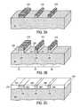
FIG. 2 is illustrated inFIGS. 3A-3G . In a particular embodiment, the fabrication begins with a “bulk”silicon monocrystalline substrate 201. In certain embodiments of the present invention, thesubstrate 201 is a silicon semiconductor having a doped epitaxial region with either p-type or n-type conductivity with an impurity concentration level of 1×10¹⁶-1×10¹⁹atoms/cm3. In another embodiment of the present invention thesubstrate 201 is a silicon semiconductor having an undoped, or intrinsic epitaxial silicon region. In other embodiments, thebulk substrate 201 is any other well-known semiconductor material, such as gallium arsenide (GaAs), indium antimonide (InSb), gallium antimonide (GaSb), gallium phosphide (GaP), indium phosphide (InP), or carbon nanotubes (CNT). - A mask is used to define the active regions of the transistors. The mask can be any well-known material suitable for defining the semiconductor substrate. As shown in
FIG. 3A , in an embodiment of the present invention,mask 310 is formed of a dielectric material that has been lithographically defined and etched. In another embodiment,mask 310 is itself a photo-definable material. In a particular embodiment, as shown inFIG. 3A , maskinglayer 310 can be a composite stack of materials, such as an oxide/nitride stack. If maskinglayer 310 is a dielectric material, commonly known techniques, such as chemical vapor deposition (CVD), low pressure chemical vapor deposition (LPCVD), plasma enhanced chemical vapor deposition (PECVD), or even spin on processes may be used to deposit the mask material while commonly known lithography and etching process may be used to define the mask. In an embodiment of the present invention, the minimum lithographic dimension is used to define the width of themask 310. In another embodiment, the minimum width of themask 310 is sub-lithographic, formed by commonly known techniques such as dry develop, oxidation/strip, or spacer-based processes. In a particular embodiment of the present invention, the width ofmask 310 is less than 30 nanometers, and more particularly, less than 20 nanometers. - As shown in
FIG. 3B , once maskinglayer 310 has been defined, a portion of the semiconductor onbulk substrate 201 is etched using commonly known methods to form recesses ortrenches 320 on the substrate in alignment withmask 310. The isolation etch defining the active regions has sufficient depth to isolate individual devices from one another and form a gate-coupled sidewall of adequate height to achieve the maximum desired channel width of the non-planar transistors. In a particular embodiment of the present invention,trenches 320 are etched to a depth equal to the maximum desired non-planar transistor channel width plus about 100 Å to about 500 Å to accommodate a dielectric isolation region. In still another embodiment, thetrenches 320 are etched to a depth of approximately 1500 Å to 3000 Å. - As shown in
FIG. 3C , thetrenches 320 are then filled with a dielectric to form shallow trench isolation (STI)regions 210 onsubstrate 201. In an embodiment of the present invention, a liner of oxide or nitride on the bottom and sidewalls of thetrenches 320 is formed by commonly known methods, such as thermal oxidation or nitridation. Next, thetrenches 320 are filled by blanket depositing an oxide over the liner by, for example, a high-density plasma (HDP) chemical vapor deposition process. The deposition process will also form dielectric on the top surfaces of themask 310. The fill dielectric layer can then be removed from the top ofmask 310 by chemical, mechanical, or electrochemical, polishing techniques. The polishing is continued until themask 310 is revealed, formingisolation regions 210, as shown inFIG. 3C . In a particular embodiment of the present invention, commonly known methods are used to selectively remove themask 310. In another embodiment, as shown inFIG. 3C , a portion ofmask 310 is retained. - If desired, wells can then be selectively formed for pMOS and nMOS transistors. Wells can be formed using any commonly known technique to dope the active regions to a desired impurity concentration. In embodiments of the present invention,
active regions bottom planes FIG. 3C . In embodiments of the present invention, after the selective well implant and mask strip, a commonly known clean, such as HF, removes either themask 310 or native oxides from the active regiontop surfaces top surfaces - The isolation regions can then be selectively protected with a masking material to allow selective definition of the non-planar devices. In an embodiment, as shown in
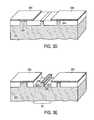
FIG. 3D ,mask 330 is formed in a manner similar to that described above with reference toFIG. 3A .Mask 330 can be either a photo-definable material or a commonly known “hard” mask material that was patterned with common lithography and etch techniques. In the embodiment depicted inFIG. 3D ,mask 330 is a photo-definable material, a photo resist. As shown inFIG. 3D ,mask 330 is used to protectisolation regions 210 bordering theactive region 204 ofplanar device 10 andactive region 224. If desired, additional mask layers may be utilized to selectively protect various other isolation regions. - Next, the isolation regions not protected by a mask are etched back, or recessed, to expose the sidewalls of the active area of the non-planar transistors. As shown in
FIG. 3E ,isolation regions 210 not protected bymask 330 are etched back without significantly etching the semiconductoractive area 224, exposing at least a portion ofsemiconductor sidewalls isolation regions 210 can be recessed with an etchant comprising a fluorine ion, such as HF. In some embodiments,isolation regions 210 are recessed using a commonly known anisotropic etch, such as a plasma or RIE process using an etchant gas such as, but not limited to, C2F6. In a further embodiment, an anisotropic etch can be followed by an isotropic etch, such as a commonly known dry process using a gas such as NF3, or a commonly known wet process such as HF, to completely remove the isolation dielectric from at least a portion of the semiconductor active region sidewalls. In some embodiments, only a portion of the unprotected isolation regions is removed during the recess etch. In a particular embodiment (not pictured), the recess etch is selective to the isolation liner material over the isolation fill material, such that the isolation recess etch is deeper along the liner region immediately adjacent to the active region than in the isolation fill region. In this manner, the width of the recess etch can then be very tightly controlled by the width of the liner, enabling a high transistor packing density. - The isolation regions are selectively recessed by an amount which, when added to a subsequent amount of unselective, or blanket recess etching, achieves the desired final gate-coupled sidewall height for the designed non-planar transistor channel width. A transistor's final gate-coupled sidewall height is determined by the cumulative amount, or depth, the adjacent isolation region is recessed. The isolation recess depth is limited by the demands of device isolation and moderate aspect ratios. For example, subsequent processing can result in inadvertent spacer artifacts if the isolation recess produces aspects ratios that are too aggressive. In a particular embodiment of the present invention, a portion of the isolation region is recessed so that the final isolation thickness is about 200 Å to about 300 Å. In other embodiments, the final isolation thickness is significantly more than about 300 Å. In an embodiment of the present invention,
isolation regions 210 are recessed by approximately the same amount as the width dimension of thetop surface 238 of the semiconductoractive region 224. In other embodiments, theisolation regions 210 are recessed by a significantly larger amount than the width dimension of thetop surface 238. - In an embodiment of the present invention, as shown in
FIG. 3F , themask 330 is then removed by commonly known means and asecond mask 340 is formed in a fashion similar as that previously discussed in reference toFIG. 3D .Mask 340 protects theactive region 224 while theisolation regions 210 surroundingactive region 244 are recessed as described above in reference toFIG. 3E . In this embodiment, a different sidewall height can be achieved for244 than that of224, thereby forming anon-planar transistor 30 having a different channel width thannon-planar transistor 20. It should be appreciated that the process of selectively masking a portion of the isolation regions and recess etching the isolation regions by a specific amount can be repeated a number of times and in a number of ways to achieve a menu of gate-coupled sidewall heights, corresponding to a menu of non-planar transistor channel widths, in accordance with the present invention. - Once the selective isolation recess etches are completed, all isolation masks are removed with commonly known techniques. If desired, a final clean, such as HF, may then be performed on all active regions, further recessing all isolation regions. In a particular embodiment of the present invention, additional sacrificial oxidation and blanket oxide etches or cleans are performed to both improve the semiconductor surface quality and further tailor the shape of the active regions through corner rounding, feature shrinking, etc.
- A gate dielectric can then be formed over the active regions in a manner dependent on the type of non-planar device (dual-gate, tri-gate, etc.). In a tri-gate embodiment of the present invention, as shown in
FIG. 3G , agate dielectric layer 212 is formed on the top surface of each of theactive regions gate dielectric layer 212 is a silicon dioxide dielectric film grown with a dry/wet oxidation process. In an embodiment of the present invention, thegate dielectric film 212 is a deposited high dielectric constant (high-K) metal oxide dielectric, such as tantalum pentaoxide, titanium oxide, hafnium oxide, zirconium oxide, aluminum oxide, or another high-K dielectric, such as barium strontium titanate (BST). A high-K film can be formed by well-known techniques, such as chemical vapor deposition (CVD) and atomic layer deposition (ALD). - A gate electrode is then formed over each active region. In an embodiment of the present invention, the
gate electrode 213, as shown inFIG. 3G , is formed on thegate dielectric layer 212 over thetop surfaces gate dielectric 212 along thesidewalls gate electrode 213 is formed by well-known techniques, such as blanket depositing a gate electrode material over the substrate and then patterning the gate electrode material. In other embodiments of the present invention, the gate electrode is formed using “replacement gate” methods. In such embodiments, the gate electrode utilizes a fill and polish technique similar to those commonly employed in damascene metallization technology, whereby the recessed isolation regions may be completely filled with gate electrode material. - In an embodiment of the present invention,
source regions 216 anddrain regions 217 fortransistors gate electrode 213, as shown inFIG. 3G . For a pMOS transistor, the active region is doped to p-type conductivity and to a concentration of 1×10¹⁹-1×10²¹atoms/cm3. For an nMOS transistor, the active is doped with n-type conductivity ions to a concentration of 1×10¹⁹-1×10²¹atoms/cm3. At this point the CMOS transistor of the present invention is substantially complete and only device interconnection remains. - Although the invention has been described in language specific to structural features and/or methodological acts, it is to be understood that the invention defined in the appended claims is not necessarily limited to the specific features or acts described. Rather, the specific features and acts are disclosed as particularly graceful implementations of the claimed invention.
Claims (20)
1. A device comprising:
a planar transistor and a non-planar transistor on a bulk semiconductor substrate.
2. The device ofclaim 1 , wherein said planar transistor is in a microprocessor core and said non-planar transistor is in a microprocessor SRAM region.
3. The device ofclaim 1 , wherein said planar transistor has a smaller channel width than that of said non-planar transistor.
4. A semiconductor device comprising:
a first active region having sidewalls substantially covered by an adjacent isolation region on a bulk semiconductor substrate;
a second active region having sidewalls extending above a top surface of an adjacent isolation region on said bulk semiconductor substrate;
a first gate insulator on a top surface of said first active region and a second gate insulator adjacent to at least a portion of said sidewalls of said second active region;
a first gate electrode on said first gate insulator and a second gate electrode adjacent to said second gate insulator; and
a first pair of source/drain regions on opposite sides of said first gate electrode and a second pair of source/drain regions on opposite sides of said second gate electrode.
5. The device ofclaim 4 , wherein said second gate insulator is on a top surface of said second active region and said second gate electrode is on said second gate insulator.
6. The device ofclaim 4 , wherein said first gate electrode and said second gate electrode are physically connected.
7. A device comprising:
a first multi-gate transistor having a first channel width and a second multi-gate transistor having a second channel width on a bulk semiconductor substrate, wherein said first channel width is different than said second channel width.
8. The device ofclaim 7 , wherein said first multi-gate transistor has a first gate-coupled sidewall height and said second multi-gate transistor has a second gate-coupled sidewall height different than said first gate coupled sidewall height.
9. The device ofclaim 7 , further comprising a single-gate transistor on said bulk semiconductor substrate.
10. A method of forming planar and non-planar transistors comprising:
forming a first active region having sidewalls adjacent to a first isolation region on a bulk semiconductor substrate;
forming a second active region having sidewalls adjacent to a second isolation region on said bulk semiconductor substrate;
exposing at least a portion of said sidewalls of said second active region by recessing a top surface of said second isolation region;
forming a first gate insulator on said top surface of said first active region;
forming a second gate insulator adjacent to at least a portion of said sidewalls of said second active region;
forming a first gate electrode on said first gate insulator;
forming a second gate electrode adjacent to said second gate insulator; and
forming a first pair of source/drain regions on opposite sides of said first gate electrode and a second pair of source/drain regions on opposite sides of said second gate electrode in said first active region and said second active region.
11. The method ofclaim 10 , wherein an etchant comprising a fluoride ion is used to recess said top surface of said second isolation region.
12. The method ofclaim 10 , wherein an anisotropic etch is used to recess said top surface of said second isolation region.
13. The method ofclaim 10 , wherein a liner region of said isolation region is recessed by an amount greater than an adjacent fill region of said isolation region.
14. The method ofclaim 10 , further comprising lithographically defining said second isolation region to be recessed.
15. The method ofclaim 10 , wherein a sacrificial oxide is formed on the top surface of said first and said second active region prior to recessing said top surface of said second isolation region.
16. The method ofclaim 10 , wherein forming said first and said second gate electrode comprises a replacement gate process.
17. The method ofclaim 10 , wherein defining said first and said second gate electrode includes etching said gate electrode material to substantially remove said gate electrode from said sidewalls of said second active region.
18. A method of forming non-planar transistors comprising:
forming a first active region having sidewalls adjacent to a first isolation region on a bulk semiconductor substrate;
forming a second active region having sidewalls adjacent to a second isolation region on said bulk semiconductor substrate;
recessing a top surface of said first isolation region by a first amount to expose at least a portion of said sidewalls of said first active region;
recessing a top surface of said second isolation region to by a second amount to expose at least a portion of said sidewalls of said second active region, said second amount of recess being different than said first amount of recess;
forming a first gate insulator adjacent to at least a portion of said sidewalls of said first active region and forming a second gate insulator adjacent to at least a portion of said sidewalls of said second active region;
forming a first gate electrode adjacent to said first gate insulator and forming a second gate electrode adjacent to said second gate insulator; and
forming a first pair of source/drain regions on opposite sides of said first gate electrode and a second pair of source/drain regions on opposite sides of said second gate electrode.
19. The method ofclaim 18 further comprising:
forming a first gate insulator and first gate electrode on a top surface of said first active region; and
forming a second gate insulator and second gate electrode on a top surface of said second active region.
20. The method ofclaim 18 , further comprising blanket etching a sacrificial oxide prior to forming said first insulator and said second gate insulator.
Priority Applications (7)
| Application Number | Priority Date | Filing Date | Title |
|---|---|---|---|
| US11/238,444US7479421B2 (en) | 2005-09-28 | 2005-09-28 | Process for integrating planar and non-planar CMOS transistors on a bulk substrate and article made thereby |
| TW095134963ATWI321830B (en) | 2005-09-28 | 2006-09-21 | Process for integrating planar and non-planar cmos transistors on a bulk substrate and article made thereby |
| CN2006800355214ACN101292346B (en) | 2005-09-28 | 2006-09-26 | Process for integrating planar and non-planar cmos transistors on a bulk substrate and article made thereby |
| EP06815547AEP1929516A2 (en) | 2005-09-28 | 2006-09-26 | Process for integrating planar and non-planar cmos transistors on a bulk substrate and article made thereby |
| KR1020087007431AKR101095188B1 (en) | 2005-09-28 | 2006-09-26 | Process for integrating planar and non-planar CMOS transistors on a bulk substrate and articles made thereby |
| PCT/US2006/037634WO2007038575A2 (en) | 2005-09-28 | 2006-09-26 | Process for integrating planar and non-planar cmos transistors on a bulk substrate and article made thereby |
| US12/333,248US8193567B2 (en) | 2005-09-28 | 2008-12-11 | Process for integrating planar and non-planar CMOS transistors on a bulk substrate and article made thereby |
Applications Claiming Priority (1)
| Application Number | Priority Date | Filing Date | Title |
|---|---|---|---|
| US11/238,444US7479421B2 (en) | 2005-09-28 | 2005-09-28 | Process for integrating planar and non-planar CMOS transistors on a bulk substrate and article made thereby |
Related Child Applications (1)
| Application Number | Title | Priority Date | Filing Date |
|---|---|---|---|
| US12/333,248DivisionUS8193567B2 (en) | 2005-09-28 | 2008-12-11 | Process for integrating planar and non-planar CMOS transistors on a bulk substrate and article made thereby |
Publications (2)
| Publication Number | Publication Date |
|---|---|
| US20070069293A1true US20070069293A1 (en) | 2007-03-29 |
| US7479421B2 US7479421B2 (en) | 2009-01-20 |
Family
ID=37668169
Family Applications (2)
| Application Number | Title | Priority Date | Filing Date |
|---|---|---|---|
| US11/238,444Expired - Fee RelatedUS7479421B2 (en) | 2005-09-28 | 2005-09-28 | Process for integrating planar and non-planar CMOS transistors on a bulk substrate and article made thereby |
| US12/333,248Expired - Fee RelatedUS8193567B2 (en) | 2005-09-28 | 2008-12-11 | Process for integrating planar and non-planar CMOS transistors on a bulk substrate and article made thereby |
Family Applications After (1)
| Application Number | Title | Priority Date | Filing Date |
|---|---|---|---|
| US12/333,248Expired - Fee RelatedUS8193567B2 (en) | 2005-09-28 | 2008-12-11 | Process for integrating planar and non-planar CMOS transistors on a bulk substrate and article made thereby |
Country Status (6)
| Country | Link |
|---|---|
| US (2) | US7479421B2 (en) |
| EP (1) | EP1929516A2 (en) |
| KR (1) | KR101095188B1 (en) |
| CN (1) | CN101292346B (en) |
| TW (1) | TWI321830B (en) |
| WO (1) | WO2007038575A2 (en) |
Cited By (49)
| Publication number | Priority date | Publication date | Assignee | Title |
|---|---|---|---|---|
| US20070010078A1 (en)* | 2005-07-07 | 2007-01-11 | Micron Technology, Inc. | Methods of forming integrated circuitry and methods of forming local interconnects |
| US20070138514A1 (en)* | 2005-12-21 | 2007-06-21 | Chang Peter L | Integration of planar and tri-gate devices on the same substrate |
| US20070170521A1 (en)* | 2006-01-12 | 2007-07-26 | International Business Machines Corporation | Method and structure to process thick and thin fins and variable fin to fin spacing |
| US20070170474A1 (en)* | 2006-01-24 | 2007-07-26 | Kabushiki Kaisha Toshiba | Semiconductor device and method of fabricating the same |
| US20070281454A1 (en)* | 2006-05-30 | 2007-12-06 | Dong Sun Sheen | Method of manufacturing semiconductor device for formation of pin transistor |
| US20080142907A1 (en)* | 2006-12-18 | 2008-06-19 | Franz Kuttner | Isolated multigate fet circuit blocks with different ground potentials |
| US20080157225A1 (en)* | 2006-12-29 | 2008-07-03 | Suman Datta | SRAM and logic transistors with variable height multi-gate transistor architecture |
| US20080157130A1 (en)* | 2006-12-29 | 2008-07-03 | Chang Peter L D | Expitaxial fabrication of fins for FinFET devices |
| US20090057780A1 (en)* | 2007-08-27 | 2009-03-05 | International Business Machines Corporation | Finfet structure including multiple semiconductor fin channel heights |
| US20090283837A1 (en)* | 2008-05-13 | 2009-11-19 | Frank Huebinger | Semiconductor Devices and Methods of Manufacture Thereof |
| US20090302374A1 (en)* | 2008-06-04 | 2009-12-10 | Anderson Brent A | Differential Nitride Pullback to Create Differential NFET to PFET Divots for Improved Performance Versus Leakage |
| US20090315114A1 (en)* | 2008-06-23 | 2009-12-24 | Intel Corporation | Stress in trigate devices using complimentary gate fill materials |
| US20090321836A1 (en)* | 2008-06-30 | 2009-12-31 | Andy Wei | Double gate and tri-gate transistor formed on a bulk substrate and method for forming the transistor |
| US20100032763A1 (en)* | 2008-08-06 | 2010-02-11 | Ravi Pillarisetty | Multiple-gate transistors and processes of making same |
| US20100167477A1 (en)* | 2007-02-26 | 2010-07-01 | International Business Machines Corporation | Localized temperature control during rapid thermal anneal |
| US20100173500A1 (en)* | 2007-02-26 | 2010-07-08 | International Business Machines Corporation | Semiconductor wafer structure with balanced reflectance and absorption characteristics for rapid thermal anneal uniformity |
| WO2010141708A1 (en)* | 2009-06-03 | 2010-12-09 | Qualcomm Incorporated | Apparatus and method to fabricate an electronic device |
| FR2961951A1 (en)* | 2010-06-23 | 2011-12-30 | Commissariat Energie Atomique | EFFECTIVE GRID WIDTH TRANSISTOR INCREASED, SEMICONDUCTOR DEVICE COMPRISING SUCH A TRANSISTOR AND METHOD OF MAKING SAME |
| US8183646B2 (en) | 2005-02-23 | 2012-05-22 | Intel Corporation | Field effect transistor with narrow bandgap source and drain regions and method of fabrication |
| US20120202330A1 (en)* | 2005-12-02 | 2012-08-09 | Nec Corporation | Semiconductor device and method of manufacturing the same |
| US8294180B2 (en) | 2005-09-28 | 2012-10-23 | Intel Corporation | CMOS devices with a single work function gate electrode and method of fabrication |
| US20120280365A1 (en)* | 2009-11-09 | 2012-11-08 | International Business Machines Corporation | Device having and method for forming fins with multiple widths |
| DE102008020140B4 (en)* | 2007-04-24 | 2013-01-17 | Infineon Technologies Ag | Mesh arrangement for field effect transistors and method for their production |
| US20130052781A1 (en)* | 2011-08-25 | 2013-02-28 | Sheng-Huei Dai | Method of Forming Non-planar FET |
| JP2013143437A (en)* | 2012-01-10 | 2013-07-22 | Renesas Electronics Corp | Semiconductor device and manufacturing method of the same |
| US8502351B2 (en) | 2004-10-25 | 2013-08-06 | Intel Corporation | Nonplanar device with thinned lower body portion and method of fabrication |
| US8581258B2 (en) | 2005-06-21 | 2013-11-12 | Intel Corporation | Semiconductor device structures and methods of forming semiconductor structures |
| US20150111355A1 (en)* | 2009-11-20 | 2015-04-23 | Taiwan Semiconductor Manufacturing Company, Ltd. | FinFETs with Different Fin Heights |
| US9048260B2 (en) | 2011-12-31 | 2015-06-02 | Intel Corporation | Method of forming a semiconductor device with tall fins and using hard mask etch stops |
| US9074295B2 (en) | 2013-03-15 | 2015-07-07 | Raytheon Company | Methods of etching carbon nanotube sheet material for electrical circuit and thin film thermal structure applications |
| US20150236164A1 (en)* | 2011-08-23 | 2015-08-20 | Micron Technology, Inc. | Semiconductor device structures and arrays of vertical transistor devices |
| WO2015195134A1 (en) | 2014-06-20 | 2015-12-23 | Intel Corporation | Monolithic integration of high voltage transistors & low voltage non-planar transistors |
| US9337307B2 (en) | 2005-06-15 | 2016-05-10 | Intel Corporation | Method for fabricating transistor with thinned channel |
| US20160276482A1 (en)* | 2015-03-20 | 2016-09-22 | Sung-min Kim | Semiconductor device including active fin |
| US20160293730A1 (en)* | 2012-06-14 | 2016-10-06 | Taiwan Semiconductor Manufacturing Company, Ltd. | Structure and Method for a Field Effect Transistor |
| EP3182452A1 (en)* | 2012-09-24 | 2017-06-21 | Intel Corporation | Precision resistor for non-planar semiconductor device architecture |
| US9711410B2 (en) | 2011-12-22 | 2017-07-18 | Intel Corporation | Semiconductor device having a necked semiconductor body and method of forming semiconductor bodies of varying width |
| CN108231874A (en)* | 2016-12-14 | 2018-06-29 | 台湾积体电路制造股份有限公司 | Grid structure |
| WO2019132928A1 (en)* | 2017-12-28 | 2019-07-04 | Intel Corporation | Group iii-nitride (iii-n) logic and rf devices and their methods of fabrication |
| CN110098186A (en)* | 2013-03-30 | 2019-08-06 | 英特尔公司 | Planar device in transistor architecture based on fin |
| US20210366779A1 (en)* | 2015-12-30 | 2021-11-25 | Taiwan Semiconductor Manufacturing Company, Ltd. | Semiconductor device and a method for fabricating the same |
| US11289572B1 (en) | 2020-10-26 | 2022-03-29 | United Microelectronics Corp. | Semiconductor device |
| CN114530447A (en)* | 2022-04-24 | 2022-05-24 | 合肥晶合集成电路股份有限公司 | Semiconductor structure and manufacturing method thereof |
| US20220285344A1 (en)* | 2020-03-13 | 2022-09-08 | Taiwan Semiconductor Manufacturing Company, Ltd. | Method to embed planar fets with finfets |
| US11610887B2 (en)* | 2019-01-09 | 2023-03-21 | Intel Corporation | Side-by-side integration of III-n transistors and thin-film transistors |
| US11749759B2 (en)* | 2012-01-31 | 2023-09-05 | Taiwan Semiconductor Manufacturing Company, Ltd. | Decoupling FinFET capacitors |
| US20230317720A1 (en)* | 2019-01-25 | 2023-10-05 | Intel Corporation | Buried channel structure integrated with non-planar structures |
| US12087634B2 (en)* | 2021-05-07 | 2024-09-10 | Taiwan Semiconductor Manufacturing Co., Ltd. | Methods for improvement of photoresist patterning profile |
| USRE50457E1 (en)* | 2007-05-09 | 2025-06-10 | Sony Group Corporation | Semiconductor device and semiconductor device manufacturing method |
Families Citing this family (72)
| Publication number | Priority date | Publication date | Assignee | Title |
|---|---|---|---|---|
| US7456476B2 (en) | 2003-06-27 | 2008-11-25 | Intel Corporation | Nonplanar semiconductor device with partially or fully wrapped around gate electrode and methods of fabrication |
| US7268058B2 (en)* | 2004-01-16 | 2007-09-11 | Intel Corporation | Tri-gate transistors and methods to fabricate same |
| US7042009B2 (en) | 2004-06-30 | 2006-05-09 | Intel Corporation | High mobility tri-gate devices and methods of fabrication |
| US7332439B2 (en)* | 2004-09-29 | 2008-02-19 | Intel Corporation | Metal gate transistors with epitaxial source and drain regions |
| KR100618900B1 (en)* | 2005-06-13 | 2006-09-01 | 삼성전자주식회사 | Method for manufacturing a MOS field effect transistor having a multi-channel and a MOS field effect transistor having a multi-channel manufactured according to the |
| US7279375B2 (en)* | 2005-06-30 | 2007-10-09 | Intel Corporation | Block contact architectures for nanoscale channel transistors |
| KR100641944B1 (en)* | 2005-07-21 | 2006-11-02 | 주식회사 하이닉스반도체 | Transistor of semiconductor device and forming method thereof |
| US7485503B2 (en) | 2005-11-30 | 2009-02-03 | Intel Corporation | Dielectric interface for group III-V semiconductor device |
| EP2062297A1 (en)* | 2006-04-07 | 2009-05-27 | Koninklijke Philips Electronics N.V. | Co-integration of multi-gate fet with other fet devices in cmos technology |
| US8143646B2 (en) | 2006-08-02 | 2012-03-27 | Intel Corporation | Stacking fault and twin blocking barrier for integrating III-V on Si |
| US7679166B2 (en) | 2007-02-26 | 2010-03-16 | International Business Machines Corporation | Localized temperature control during rapid thermal anneal |
| US7692275B2 (en) | 2007-02-26 | 2010-04-06 | International Business Machines Corporation | Structure and method for device-specific fill for improved anneal uniformity |
| US7821061B2 (en)* | 2007-03-29 | 2010-10-26 | Intel Corporation | Silicon germanium and germanium multigate and nanowire structures for logic and multilevel memory applications |
| US20080283910A1 (en)* | 2007-05-15 | 2008-11-20 | Qimonda Ag | Integrated circuit and method of forming an integrated circuit |
| JP2009054946A (en)* | 2007-08-29 | 2009-03-12 | Seiko Instruments Inc | Semiconductor device and manufacturing method thereof |
| KR101263648B1 (en)* | 2007-08-31 | 2013-05-21 | 삼성전자주식회사 | Fin field effect transistor and method of manufacturing the same |
| US8211786B2 (en)* | 2008-02-28 | 2012-07-03 | International Business Machines Corporation | CMOS structure including non-planar hybrid orientation substrate with planar gate electrodes and method for fabrication |
| US8106459B2 (en)* | 2008-05-06 | 2012-01-31 | Taiwan Semiconductor Manufacturing Company, Ltd. | FinFETs having dielectric punch-through stoppers |
| DE102008059646B4 (en)* | 2008-11-28 | 2010-12-30 | Advanced Micro Devices, Inc., Sunnyvale | A method of manufacturing a semiconductor device as a multi-gate transistor having lands of a length defined by the gate electrode and semiconductor device |
| US7927942B2 (en) | 2008-12-19 | 2011-04-19 | Asm International N.V. | Selective silicide process |
| US9379011B2 (en) | 2008-12-19 | 2016-06-28 | Asm International N.V. | Methods for depositing nickel films and for making nickel silicide and nickel germanide |
| US8293616B2 (en) | 2009-02-24 | 2012-10-23 | Taiwan Semiconductor Manufacturing Company, Ltd. | Methods of fabrication of semiconductor devices with low capacitance |
| US8138543B2 (en) | 2009-11-18 | 2012-03-20 | International Business Machines Corporation | Hybrid FinFET/planar SOI FETs |
| US8659072B2 (en)* | 2010-09-24 | 2014-02-25 | Taiwan Semiconductor Manufacturing Company, Ltd. | Series FinFET implementation schemes |
| US8354319B2 (en)* | 2010-10-15 | 2013-01-15 | International Business Machines Corporation | Integrated planar and multiple gate FETs |
| US8524546B2 (en) | 2010-10-22 | 2013-09-03 | International Business Machines Corporation | Formation of multi-height MUGFET |
| US8524545B2 (en) | 2010-10-22 | 2013-09-03 | International Business Machines Corporation | Simultaneous formation of FinFET and MUGFET |
| US8871617B2 (en) | 2011-04-22 | 2014-10-28 | Asm Ip Holding B.V. | Deposition and reduction of mixed metal oxide thin films |
| US8685825B2 (en)* | 2011-07-27 | 2014-04-01 | Advanced Ion Beam Technology, Inc. | Replacement source/drain finFET fabrication |
| US8871584B2 (en) | 2011-07-27 | 2014-10-28 | Advanced Ion Beam Technology, Inc. | Replacement source/drain finFET fabrication |
| US9105660B2 (en) | 2011-08-17 | 2015-08-11 | United Microelectronics Corp. | Fin-FET and method of forming the same |
| US9287385B2 (en) | 2011-09-01 | 2016-03-15 | Taiwan Semiconductor Manufacturing Company, Ltd. | Multi-fin device and method of making same |
| KR101964262B1 (en)* | 2011-11-25 | 2019-04-02 | 삼성전자주식회사 | Semiconductor device and method of manufacturing same |
| US8563376B2 (en) | 2011-12-16 | 2013-10-22 | International Business Machines Corporation | Hybrid CMOS nanowire mesh device and bulk CMOS device |
| US8709888B2 (en) | 2011-12-16 | 2014-04-29 | International Business Machines Corporation | Hybrid CMOS nanowire mesh device and PDSOI device |
| US8722472B2 (en) | 2011-12-16 | 2014-05-13 | International Business Machines Corporation | Hybrid CMOS nanowire mesh device and FINFET device |
| US9012284B2 (en) | 2011-12-23 | 2015-04-21 | Intel Corporation | Nanowire transistor devices and forming techniques |
| US9224810B2 (en) | 2011-12-23 | 2015-12-29 | Intel Corporation | CMOS nanowire structure |
| US8587068B2 (en) | 2012-01-26 | 2013-11-19 | International Business Machines Corporation | SRAM with hybrid FinFET and planar transistors |
| KR101678405B1 (en)* | 2012-07-27 | 2016-11-22 | 인텔 코포레이션 | Nanowire transistor devices and forming techniques |
| US8759874B1 (en) | 2012-11-30 | 2014-06-24 | Stmicroelectronics, Inc. | FinFET device with isolated channel |
| KR101983633B1 (en) | 2012-11-30 | 2019-05-29 | 삼성전자 주식회사 | Semiconductor device and fabricated method thereof |
| US8956942B2 (en) | 2012-12-21 | 2015-02-17 | Stmicroelectronics, Inc. | Method of forming a fully substrate-isolated FinFET transistor |
| US9318367B2 (en) | 2013-02-27 | 2016-04-19 | Taiwan Semiconductor Manufacturing Company, Ltd. | FinFET structure with different fin heights and method for forming the same |
| US10438856B2 (en) | 2013-04-03 | 2019-10-08 | Stmicroelectronics, Inc. | Methods and devices for enhancing mobility of charge carriers |
| US20150021698A1 (en)* | 2013-07-18 | 2015-01-22 | International Business Machines Corporation | Intrinsic Channel Planar Field Effect Transistors Having Multiple Threshold Voltages |
| US9064989B2 (en) | 2013-08-30 | 2015-06-23 | Taiwan Semiconductor Manufacturing Company Limited | Photo diode and method of forming the same |
| US9153694B2 (en) | 2013-09-04 | 2015-10-06 | Globalfoundries Inc. | Methods of forming contact structures on finfet semiconductor devices and the resulting devices |
| EP2866264A1 (en) | 2013-10-22 | 2015-04-29 | IMEC vzw | Method for manufacturing a field effect transistor of a non-planar type |
| DE102014220672A1 (en) | 2013-10-22 | 2015-05-07 | Semiconductor Energy Laboratory Co., Ltd. | Semiconductor device |
| US9147683B2 (en) | 2014-02-18 | 2015-09-29 | International Business Machines Corporation | CMOS transistors including gate spacers of the same thickness |
| US9947772B2 (en) | 2014-03-31 | 2018-04-17 | Stmicroelectronics, Inc. | SOI FinFET transistor with strained channel |
| JP6537341B2 (en)* | 2014-05-07 | 2019-07-03 | 株式会社半導体エネルギー研究所 | Semiconductor device |
| US9425275B2 (en)* | 2014-06-13 | 2016-08-23 | Samsung Electronics Co., Ltd. | Integrated circuit chips having field effect transistors with different gate designs |
| US9502518B2 (en) | 2014-06-23 | 2016-11-22 | Stmicroelectronics, Inc. | Multi-channel gate-all-around FET |
| US9362405B1 (en)* | 2014-12-04 | 2016-06-07 | Globalfoundries Inc. | Channel cladding last process flow for forming a channel region on a FinFET device |
| US9461110B1 (en)* | 2015-04-30 | 2016-10-04 | Taiwan Semiconductor Manufacturing Company, Ltd. | FETs and methods of forming FETs |
| US9666493B2 (en) | 2015-06-24 | 2017-05-30 | International Business Machines Corporation | Semiconductor device structure with 110-PFET and 111-NFET curent flow direction |
| US9905467B2 (en)* | 2015-09-04 | 2018-02-27 | Taiwan Semiconductor Manufacturing Company, Ltd. | Semiconductor device and manufacturing method thereof |
| US9607842B1 (en) | 2015-10-02 | 2017-03-28 | Asm Ip Holding B.V. | Methods of forming metal silicides |
| US9899378B2 (en) | 2015-12-14 | 2018-02-20 | International Business Machines Corporation | Simultaneously fabricating a high voltage transistor and a finFET |
| EP3182461B1 (en)* | 2015-12-16 | 2022-08-03 | IMEC vzw | Method for fabricating finfet technology with locally higher fin-to-fin pitch |
| US9502407B1 (en)* | 2015-12-16 | 2016-11-22 | International Business Machines Corporation | Integrating a planar field effect transistor (FET) with a vertical FET |
| US9601497B1 (en) | 2016-04-28 | 2017-03-21 | Taiwan Semiconductor Manufacturing Co., Ltd. | Static random access memory and method of manufacturing the same |
| US9916978B2 (en) | 2016-06-02 | 2018-03-13 | United Microelectronics Corporation | Method for fabricating a Fin field effect transistor (FinFET) |
| US10541205B1 (en)* | 2017-02-14 | 2020-01-21 | Intel Corporation | Manufacture of interconnects for integration of multiple integrated circuits |
| CN108933134B (en)* | 2017-05-24 | 2020-09-25 | 清华大学 | Semiconductor device |
| US10483167B2 (en)* | 2017-08-15 | 2019-11-19 | Taiwan Semiconductor Manufacturing Co., Ltd. | Method for manufacturing dual FinFET device |
| KR102721833B1 (en)* | 2018-10-08 | 2024-10-24 | 삼성전자주식회사 | Semiconductor Device |
| CN109545802B (en)* | 2018-12-14 | 2021-01-12 | 上海微阱电子科技有限公司 | Semiconductor-on-insulator device structure and forming method |
| TWI723878B (en)* | 2020-01-30 | 2021-04-01 | 旺宏電子股份有限公司 | Multi-gate transistor and memory device using the same |
| US20240071833A1 (en)* | 2022-08-25 | 2024-02-29 | Taiwan Semiconductor Manufacturing Company, Ltd. | Hybrid fin-dielectric semiconductor device |
Citations (46)
| Publication number | Priority date | Publication date | Assignee | Title |
|---|---|---|---|---|
| US5682048A (en)* | 1995-05-19 | 1997-10-28 | Nissan Motor Co., Ltd. | Groove-type semiconductor device |
| US5889304A (en)* | 1996-06-28 | 1999-03-30 | Kabushiki Kaisha Toshiba | Nonvolatile semiconductor memory device |
| US5908313A (en)* | 1996-12-31 | 1999-06-01 | Intel Corporation | Method of forming a transistor |
| US6013926A (en)* | 1996-11-20 | 2000-01-11 | Mitsubishi Denki Kabushiki Kaisha | Semiconductor device with refractory metal element |
| US6054355A (en)* | 1997-06-30 | 2000-04-25 | Kabushiki Kaisha Toshiba | Method of manufacturing a semiconductor device which includes forming a dummy gate |
| US6120846A (en)* | 1997-12-23 | 2000-09-19 | Advanced Technology Materials, Inc. | Method for the selective deposition of bismuth based ferroelectric thin films by chemical vapor deposition |
| US6251763B1 (en)* | 1997-06-30 | 2001-06-26 | Kabushiki Kaisha Toshiba | Semiconductor device and method for manufacturing same |
| US6259135B1 (en)* | 1999-09-24 | 2001-07-10 | International Business Machines Corporation | MOS transistors structure for reducing the size of pitch limited circuits |
| US6368923B1 (en)* | 2000-04-20 | 2002-04-09 | United Microelectronics Corp. | Method of fabricating a dual metal gate having two different gate dielectric layers |
| US20020058374A1 (en)* | 2000-11-16 | 2002-05-16 | Tae-Kyun Kim | Method of forming dual-metal gates in semiconductor device |
| US6403981B1 (en)* | 2000-08-07 | 2002-06-11 | Advanced Micro Devices, Inc. | Double gate transistor having a silicon/germanium channel region |
| US20020074614A1 (en)* | 2000-12-15 | 2002-06-20 | Mitsubishi Denki Kabushiki Kaisha | Semiconductor device and manufacturing method therefor |
| US6437550B2 (en)* | 1999-12-28 | 2002-08-20 | Ricoh Company, Ltd. | Voltage generating circuit and reference voltage source circuit employing field effect transistors |
| US6555879B1 (en)* | 2002-01-11 | 2003-04-29 | Advanced Micro Devices, Inc. | SOI device with metal source/drain and method of fabrication |
| US20030102518A1 (en)* | 2001-12-04 | 2003-06-05 | International Business Machines Corporation | Finfet SRAM cell using low mobility plane for cell stability and method for forming |
| US6605498B1 (en)* | 2002-03-29 | 2003-08-12 | Intel Corporation | Semiconductor transistor having a backfilled channel material |
| US20030174534A1 (en)* | 2002-03-12 | 2003-09-18 | Clark Lawrence T. | Low standby power using shadow storage |
| US6642114B2 (en)* | 1997-01-29 | 2003-11-04 | Fujitsu Limited | Semiconductor device and method for fabricating the same |
| US20040132236A1 (en)* | 2003-01-08 | 2004-07-08 | International Business Machines Corporation | Mos transistor |
| US20040145000A1 (en)* | 2003-01-23 | 2004-07-29 | An Judy Xilin | Tri-gate and gate around MOSFET devices and methods for making same |
| US20040222473A1 (en)* | 2003-04-15 | 2004-11-11 | Tomomitsu Risaki | Semiconductor device |
| US6852559B2 (en)* | 2002-12-06 | 2005-02-08 | Hynix Semiconductor Inc. | Transistor of semiconductor device, and method for manufacturing the same |
| US20050059214A1 (en)* | 2003-09-16 | 2005-03-17 | International Business Machines Corporation | Method and structure of vertical strained silicon devices |
| US20050093075A1 (en)* | 2003-10-31 | 2005-05-05 | Bentum Ralf V. | Advanced technique for forming a transistor having raised drain and source regions |
| US6891234B1 (en)* | 2004-01-07 | 2005-05-10 | Acorn Technologies, Inc. | Transistor with workfunction-induced charge layer |
| US20050110082A1 (en)* | 2003-11-25 | 2005-05-26 | Taiwan Semiconductor Manufacturing Co., Ltd. | Semiconductor device having high drive current and method of manufacture therefor |
| US20050148131A1 (en)* | 2003-12-30 | 2005-07-07 | Brask Justin K. | Method of varying etch selectivities of a film |
| US20050145894A1 (en)* | 2003-12-30 | 2005-07-07 | Chau Robert S. | Replacement gate flow facilitating high yield and incorporation of etch stop layers and/or stressed films |
| US20050156227A1 (en)* | 2003-11-18 | 2005-07-21 | Applied Intellectual Properties Co., Ltd. | Nonvolatile memory with undercut trapping structure |
| US20050161739A1 (en)* | 2004-01-28 | 2005-07-28 | International Business Machines Corporation | Method and structure to create multiple device widths in finfet technology in both bulk and soi |
| US20050170593A1 (en)* | 2004-02-02 | 2005-08-04 | Hee-Soo Kang | Method for forming a FinFET by a damascene process |
| US20050199919A1 (en)* | 2004-03-02 | 2005-09-15 | National Institute Of Advanced Industrial Science And Technology | Semiconductor integrated circuit and method for manufacturing the same |
| US20050215014A1 (en)* | 2004-03-23 | 2005-09-29 | Young-Joon Ahn | Complementary metal oxide semiconductor (CMOS) transistors having three-dimensional channel regions and methods of forming same |
| US20050239252A1 (en)* | 2004-04-27 | 2005-10-27 | Young-Joon Ahn | Methods of forming integrated circuit devices having field effect transistors of different types in different device regions |
| US20050255642A1 (en)* | 2004-05-11 | 2005-11-17 | Chi-Wen Liu | Method of fabricating inlaid structure |
| US20050272192A1 (en)* | 2004-06-04 | 2005-12-08 | Chang-Woo Oh | Methods of forming fin field effect transistors using oxidation barrier layers and related devices |
| US7105390B2 (en)* | 2003-12-30 | 2006-09-12 | Intel Corporation | Nonplanar transistors with metal gate electrodes |
| US7105894B2 (en)* | 2003-02-27 | 2006-09-12 | Taiwan Semiconductor Manufacturing Co., Ltd. | Contacts to semiconductor fin devices |
| US20060202270A1 (en)* | 2003-10-31 | 2006-09-14 | Samsung Electronics Co., Ltd. | Fin field effect transistors having capping insulation layers |
| US7119402B2 (en)* | 2003-09-05 | 2006-10-10 | Kabushiki Kaisha Toshiba | Field effect transistor and manufacturing method thereof |
| US20060227595A1 (en)* | 2005-04-07 | 2006-10-12 | International Business Machines Corporation | Back-gate controlled read SRAM cell |
| US7154118B2 (en)* | 2004-03-31 | 2006-12-26 | Intel Corporation | Bulk non-planar transistor having strained enhanced mobility and methods of fabrication |
| US20070045748A1 (en)* | 2005-08-25 | 2007-03-01 | International Business Machines Corporation | Semiconductor structures integrating damascene-body FinFET's and planar devices on a common substrate and methods for forming such semiconductor structures |
| US20070048930A1 (en)* | 2005-09-01 | 2007-03-01 | Figura Thomas A | Peripheral gate stacks and recessed array gates |
| US20070108514A1 (en)* | 2003-04-28 | 2007-05-17 | Akira Inoue | Semiconductor device and method of fabricating the same |
| US7238564B2 (en)* | 2005-03-10 | 2007-07-03 | Taiwan Semiconductor Manufacturing Company | Method of forming a shallow trench isolation structure |
Family Cites Families (309)
| Publication number | Priority date | Publication date | Assignee | Title |
|---|---|---|---|---|
| US4231149A (en) | 1978-10-10 | 1980-11-04 | Texas Instruments Incorporated | Narrow band-gap semiconductor CCD imaging device and method of fabrication |
| JPS5673454U (en) | 1979-11-09 | 1981-06-16 | ||
| JPS59145538U (en) | 1983-03-22 | 1984-09-28 | 日本電気株式会社 | High-frequency heating high-pressure zone "Ku" molten material synthesis furnace |
| GB2156149A (en) | 1984-03-14 | 1985-10-02 | Philips Electronic Associated | Dielectrically-isolated integrated circuit manufacture |
| US4487652A (en) | 1984-03-30 | 1984-12-11 | Motorola, Inc. | Slope etch of polyimide |
| US5514885A (en) | 1986-10-09 | 1996-05-07 | Myrick; James J. | SOI methods and apparatus |
| US4818715A (en) | 1987-07-09 | 1989-04-04 | Industrial Technology Research Institute | Method of fabricating a LDDFET with self-aligned silicide |
| US4907048A (en) | 1987-11-23 | 1990-03-06 | Xerox Corporation | Double implanted LDD transistor self-aligned with gate |
| US4905063A (en)* | 1988-06-21 | 1990-02-27 | American Telephone And Telegraph Company, At&T Bell Laboratories | Floating gate memories |
| JPH0214578A (en) | 1988-07-01 | 1990-01-18 | Fujitsu Ltd | semiconductor equipment |
| JPH065856B2 (en) | 1988-07-05 | 1994-01-19 | 株式会社精工舎 | Color separation device |
| KR910010043B1 (en) | 1988-07-28 | 1991-12-10 | 한국전기통신공사 | Fine Line Width Formation Method Using Spacer |
| US4994873A (en) | 1988-10-17 | 1991-02-19 | Motorola, Inc. | Local interconnect for stacked polysilicon device |
| US5346834A (en) | 1988-11-21 | 1994-09-13 | Hitachi, Ltd. | Method for manufacturing a semiconductor device and a semiconductor memory device |
| US4906589A (en) | 1989-02-06 | 1990-03-06 | Industrial Technology Research Institute | Inverse-T LDDFET with self-aligned silicide |
| US5328810A (en) | 1990-05-07 | 1994-07-12 | Micron Technology, Inc. | Method for reducing, by a factor or 2-N, the minimum masking pitch of a photolithographic process |
| KR930003790B1 (en) | 1990-07-02 | 1993-05-10 | 삼성전자 주식회사 | Dielectrics for Capacitors in Semiconductor Devices |
| JP3061406B2 (en) | 1990-09-28 | 2000-07-10 | 株式会社東芝 | Semiconductor device |
| JP3202223B2 (en) | 1990-11-27 | 2001-08-27 | 日本電気株式会社 | Method for manufacturing transistor |
| US5521859A (en) | 1991-03-20 | 1996-05-28 | Fujitsu Limited | Semiconductor memory device having thin film transistor and method of producing the same |
| EP0510667B1 (en) | 1991-04-26 | 1996-09-11 | Canon Kabushiki Kaisha | Semiconductor device having an improved insulated gate transistor |
| JPH05152293A (en) | 1991-04-30 | 1993-06-18 | Sgs Thomson Microelectron Inc | Method for manufacturing stepped wall interconnect and gate |
| US5346836A (en) | 1991-06-06 | 1994-09-13 | Micron Technology, Inc. | Process for forming low resistance contacts between silicide areas and upper level polysilicon interconnects |
| US5292670A (en) | 1991-06-10 | 1994-03-08 | Texas Instruments Incorporated | Sidewall doping technique for SOI transistors |
| US5179037A (en) | 1991-12-24 | 1993-01-12 | Texas Instruments Incorporated | Integration of lateral and vertical quantum well transistors in the same epitaxial stack |
| US5391506A (en) | 1992-01-31 | 1995-02-21 | Kawasaki Steel Corporation | Manufacturing method for semiconductor devices with source/drain formed in substrate projection. |
| JPH05243572A (en) | 1992-02-27 | 1993-09-21 | Fujitsu Ltd | Semiconductor device |
| US5405454A (en) | 1992-03-19 | 1995-04-11 | Matsushita Electric Industrial Co., Ltd. | Electrically insulated silicon structure and producing method therefor |
| JP2572003B2 (en) | 1992-03-30 | 1997-01-16 | 三星電子株式会社 | Method of manufacturing thin film transistor having three-dimensional multi-channel structure |
| JPH0793441B2 (en) | 1992-04-24 | 1995-10-09 | ヒュンダイ エレクトロニクス インダストリーズ カンパニー リミテッド | Thin film transistor and manufacturing method thereof |
| JPH06151387A (en) | 1992-11-10 | 1994-05-31 | Nippon Telegr & Teleph Corp <Ntt> | Precision processing method of silicon |
| KR960002088B1 (en)* | 1993-02-17 | 1996-02-10 | 삼성전자주식회사 | Method of manufacturing a semiconductor device having a silicon on insulator (SOI) structure |
| US5357119A (en) | 1993-02-19 | 1994-10-18 | Board Of Regents Of The University Of California | Field effect devices having short period superlattice structures using Si and Ge |
| JPH06310547A (en) | 1993-02-25 | 1994-11-04 | Mitsubishi Electric Corp | Semiconductor device and manufacture thereof |
| EP0623963A1 (en) | 1993-05-06 | 1994-11-09 | Siemens Aktiengesellschaft | MOSFET on SOI substrate |
| US5739544A (en) | 1993-05-26 | 1998-04-14 | Matsushita Electric Industrial Co., Ltd. | Quantization functional device utilizing a resonance tunneling effect and method for producing the same |
| US5475869A (en) | 1993-05-28 | 1995-12-12 | Nec Corporation | Radio base station capable of distinguishing between interference due to collisions of outgoing call signals and an external interference noise |
| US6730549B1 (en) | 1993-06-25 | 2004-05-04 | Semiconductor Energy Laboratory Co., Ltd. | Semiconductor device and method for its preparation |
| JP3778581B2 (en) | 1993-07-05 | 2006-05-24 | 三菱電機株式会社 | Semiconductor device and manufacturing method thereof |
| US5398641A (en)* | 1993-07-27 | 1995-03-21 | Texas Instruments Incorporated | Method for p-type doping of semiconductor structures formed of group II and group VI elements |
| JP3460863B2 (en) | 1993-09-17 | 2003-10-27 | 三菱電機株式会社 | Method for manufacturing semiconductor device |
| US5479033A (en) | 1994-05-27 | 1995-12-26 | Sandia Corporation | Complementary junction heterostructure field-effect transistor |
| JP3361922B2 (en) | 1994-09-13 | 2003-01-07 | 株式会社東芝 | Semiconductor device |
| JP3378414B2 (en) | 1994-09-14 | 2003-02-17 | 株式会社東芝 | Semiconductor device |
| JPH08153880A (en)* | 1994-09-29 | 1996-06-11 | Toshiba Corp | Semiconductor device and manufacturing method thereof |
| US5602049A (en) | 1994-10-04 | 1997-02-11 | United Microelectronics Corporation | Method of fabricating a buried structure SRAM cell |
| JPH08125152A (en) | 1994-10-28 | 1996-05-17 | Canon Inc | Semiconductor device, correlation calculation device using the same, AD converter, DA converter, signal processing system |
| JP3078720B2 (en) | 1994-11-02 | 2000-08-21 | 三菱電機株式会社 | Semiconductor device and manufacturing method thereof |
| GB2295488B (en) | 1994-11-24 | 1996-11-20 | Toshiba Cambridge Res Center | Semiconductor device |
| US5716879A (en) | 1994-12-15 | 1998-02-10 | Goldstar Electron Company, Ltd. | Method of making a thin film transistor |
| JPH08204191A (en) | 1995-01-20 | 1996-08-09 | Sony Corp | Field effect transistor and method of manufacturing the same |
| US5665203A (en) | 1995-04-28 | 1997-09-09 | International Business Machines Corporation | Silicon etching method |
| KR0165398B1 (en) | 1995-05-26 | 1998-12-15 | 윤종용 | Vertical transistor manufacturing method |
| US5814545A (en) | 1995-10-02 | 1998-09-29 | Motorola, Inc. | Semiconductor device having a phosphorus doped PECVD film and a method of manufacture |
| US5658806A (en) | 1995-10-26 | 1997-08-19 | National Science Council | Method for fabricating thin-film transistor with bottom-gate or dual-gate configuration |
| US5814895A (en) | 1995-12-22 | 1998-09-29 | Sony Corporation | Static random access memory having transistor elements formed on side walls of a trench in a semiconductor substrate |
| KR100205442B1 (en) | 1995-12-26 | 1999-07-01 | 구본준 | Thin film transistor and its manufacturing method |
| US5595919A (en)* | 1996-02-20 | 1997-01-21 | Chartered Semiconductor Manufacturing Pte Ltd. | Method of making self-aligned halo process for reducing junction capacitance |
| DE19607209A1 (en) | 1996-02-26 | 1997-08-28 | Gregor Kohlruss | Cleaning device for cleaning flat objects |
| EP0802483B1 (en)* | 1996-04-18 | 2002-01-30 | STMicroelectronics S.r.l. | Semiconductor memory device with row redundancy |
| JPH09293793A (en) | 1996-04-26 | 1997-11-11 | Mitsubishi Electric Corp | Semiconductor device having thin film transistor and manufacturing method thereof |
| US5793088A (en) | 1996-06-18 | 1998-08-11 | Integrated Device Technology, Inc. | Structure for controlling threshold voltage of MOSFET |
| TW556263B (en) | 1996-07-11 | 2003-10-01 | Semiconductor Energy Lab | Semiconductor device and method of manufacturing the same |
| US5817560A (en) | 1996-09-12 | 1998-10-06 | Advanced Micro Devices, Inc. | Ultra short trench transistors and process for making same |
| US6399970B2 (en) | 1996-09-17 | 2002-06-04 | Matsushita Electric Industrial Co., Ltd. | FET having a Si/SiGeC heterojunction channel |
| US6063677A (en) | 1996-10-28 | 2000-05-16 | Texas Instruments Incorporated | Method of forming a MOSFET using a disposable gate and raised source and drain |
| US6063675A (en) | 1996-10-28 | 2000-05-16 | Texas Instruments Incorporated | Method of forming a MOSFET using a disposable gate with a sidewall dielectric |
| US6163053A (en) | 1996-11-06 | 2000-12-19 | Ricoh Company, Ltd. | Semiconductor device having opposite-polarity region under channel |
| US5827769A (en) | 1996-11-20 | 1998-10-27 | Intel Corporation | Method for fabricating a transistor with increased hot carrier resistance by nitridizing and annealing the sidewall oxide of the gate electrode |
| US5773331A (en) | 1996-12-17 | 1998-06-30 | International Business Machines Corporation | Method for making single and double gate field effect transistors with sidewall source-drain contacts |
| JPH118390A (en) | 1997-06-18 | 1999-01-12 | Mitsubishi Electric Corp | Semiconductor device and manufacturing method thereof |
| JPH1140811A (en) | 1997-07-22 | 1999-02-12 | Hitachi Ltd | Semiconductor device and manufacturing method thereof |
| US5952701A (en) | 1997-08-18 | 1999-09-14 | National Semiconductor Corporation | Design and fabrication of semiconductor structure having complementary channel-junction insulated-gate field-effect transistors whose gate electrodes have work functions close to mid-gap semiconductor value |
| US5776821A (en) | 1997-08-22 | 1998-07-07 | Vlsi Technology, Inc. | Method for forming a reduced width gate electrode |
| US6066869A (en) | 1997-10-06 | 2000-05-23 | Micron Technology, Inc. | Circuit and method for a folded bit line memory cell with vertical transistor and trench capacitor |
| US5976767A (en) | 1997-10-09 | 1999-11-02 | Micron Technology, Inc. | Ammonium hydroxide etch of photoresist masked silicon |
| US5888309A (en) | 1997-12-29 | 1999-03-30 | Taiwan Semiconductor Manufacturing Company, Ltd. | Lateral etch inhibited multiple for forming a via through a microelectronics layer susceptible to etching within a fluorine containing plasma followed by an oxygen containing plasma |
| US6117741A (en) | 1998-01-09 | 2000-09-12 | Texas Instruments Incorporated | Method of forming a transistor having an improved sidewall gate structure |
| US6294416B1 (en) | 1998-01-23 | 2001-09-25 | Texas Instruments-Acer Incorporated | Method of fabricating CMOS transistors with self-aligned planarization twin-well by using fewer mask counts |
| US6307235B1 (en) | 1998-03-30 | 2001-10-23 | Micron Technology, Inc. | Another technique for gated lateral bipolar transistors |
| US6097065A (en) | 1998-03-30 | 2000-08-01 | Micron Technology, Inc. | Circuits and methods for dual-gated transistors |
| US6087208A (en) | 1998-03-31 | 2000-07-11 | Advanced Micro Devices, Inc. | Method for increasing gate capacitance by using both high and low dielectric gate material |
| US6215190B1 (en) | 1998-05-12 | 2001-04-10 | International Business Machines Corporation | Borderless contact to diffusion with respect to gate conductor and methods for fabricating |
| US6232641B1 (en) | 1998-05-29 | 2001-05-15 | Kabushiki Kaisha Toshiba | Semiconductor apparatus having elevated source and drain structure and manufacturing method therefor |
| US6114201A (en) | 1998-06-01 | 2000-09-05 | Texas Instruments-Acer Incorporated | Method of manufacturing a multiple fin-shaped capacitor for high density DRAMs |
| US20010040907A1 (en) | 1998-06-12 | 2001-11-15 | Utpal Kumar Chakrabarti | Optical device including carbon-doped contact layers |
| US6165880A (en) | 1998-06-15 | 2000-12-26 | Taiwan Semiconductor Manufacturing Company | Double spacer technology for making self-aligned contacts (SAC) on semiconductor integrated circuits |
| US6130123A (en) | 1998-06-30 | 2000-10-10 | Intel Corporation | Method for making a complementary metal gate electrode technology |
| JP2000037842A (en) | 1998-07-27 | 2000-02-08 | Dainippon Printing Co Ltd | Electromagnetic wave absorbing cosmetic material |
| US6696366B1 (en) | 1998-08-17 | 2004-02-24 | Lam Research Corporation | Technique for etching a low capacitance dielectric layer |
| JP2000156502A (en) | 1998-09-21 | 2000-06-06 | Texas Instr Inc <Ti> | Integrated circuit and method |
| US6153485A (en) | 1998-11-09 | 2000-11-28 | Chartered Semiconductor Manufacturing Ltd. | Salicide formation on narrow poly lines by pulling back of spacer |
| US6362111B1 (en) | 1998-12-09 | 2002-03-26 | Texas Instruments Incorporated | Tunable gate linewidth reduction process |
| TW406312B (en) | 1998-12-18 | 2000-09-21 | United Microelectronics Corp | The method of etching doped poly-silicon |
| TW449919B (en) | 1998-12-18 | 2001-08-11 | Koninkl Philips Electronics Nv | A method of manufacturing a semiconductor device |
| US6380558B1 (en) | 1998-12-29 | 2002-04-30 | Semiconductor Energy Laboratory Co., Ltd. | Semiconductor device and method of fabricating the same |
| US6150222A (en) | 1999-01-07 | 2000-11-21 | Advanced Micro Devices, Inc. | Method of making a high performance transistor with elevated spacer formation and self-aligned channel regions |
| FR2788629B1 (en) | 1999-01-15 | 2003-06-20 | Commissariat Energie Atomique | TRANSISTOR MIS AND METHOD FOR FABRICATING SUCH A TRANSISTOR ON A SEMICONDUCTOR SUBSTRATE |
| US6174820B1 (en) | 1999-02-16 | 2001-01-16 | Sandia Corporation | Use of silicon oxynitride as a sacrificial material for microelectromechanical devices |
| JP2000243854A (en) | 1999-02-22 | 2000-09-08 | Toshiba Corp | Semiconductor device and manufacturing method thereof |
| US6093621A (en) | 1999-04-05 | 2000-07-25 | Vanguard International Semiconductor Corp. | Method of forming shallow trench isolation |
| US7045468B2 (en) | 1999-04-09 | 2006-05-16 | Intel Corporation | Isolated junction structure and method of manufacture |
| US6459123B1 (en) | 1999-04-30 | 2002-10-01 | Infineon Technologies Richmond, Lp | Double gated transistor |
| DE60001601T2 (en) | 1999-06-18 | 2003-12-18 | Lucent Technologies Inc., Murray Hill | Manufacturing process for manufacturing a CMOS integrated circuit with vertical transistors |
| JP2001015704A (en) | 1999-06-29 | 2001-01-19 | Hitachi Ltd | Semiconductor integrated circuit |
| US6218309B1 (en) | 1999-06-30 | 2001-04-17 | Lam Research Corporation | Method of achieving top rounding and uniform etch depths while etching shallow trench isolation features |
| US6501131B1 (en) | 1999-07-22 | 2002-12-31 | International Business Machines Corporation | Transistors having independently adjustable parameters |
| TW432594B (en) | 1999-07-31 | 2001-05-01 | Taiwan Semiconductor Mfg | Manufacturing method for shallow trench isolation |
| FR2799305B1 (en) | 1999-10-05 | 2004-06-18 | St Microelectronics Sa | METHOD FOR MANUFACTURING A SEMICONDUCTOR DEVICE WITH ENVELOPING GRID AND DEVICE OBTAINED |
| EP1091413A3 (en) | 1999-10-06 | 2005-01-12 | Lsi Logic Corporation | Fully-depleted, fully-inverted, short-length and vertical channel, dual-gate, cmos fet |
| US6541829B2 (en) | 1999-12-03 | 2003-04-01 | Kabushiki Kaisha Toshiba | Semiconductor device and method of manufacturing the same |
| US6252284B1 (en) | 1999-12-09 | 2001-06-26 | International Business Machines Corporation | Planarized silicon fin device |
| KR100311049B1 (en) | 1999-12-13 | 2001-10-12 | 윤종용 | Nonvolatile semiconductor memory device and manufacturing method thereof |
| US6303479B1 (en) | 1999-12-16 | 2001-10-16 | Spinnaker Semiconductor, Inc. | Method of manufacturing a short-channel FET with Schottky-barrier source and drain contacts |
| JP4923318B2 (en) | 1999-12-17 | 2012-04-25 | ソニー株式会社 | Nonvolatile semiconductor memory device and operation method thereof |
| CN100346926C (en) | 2000-02-23 | 2007-11-07 | 信越半导体株式会社 | Polishing method for peripheral chamfer part of wafer |
| US6483156B1 (en) | 2000-03-16 | 2002-11-19 | International Business Machines Corporation | Double planar gated SOI MOSFET structure |
| FR2806832B1 (en) | 2000-03-22 | 2002-10-25 | Commissariat Energie Atomique | METAL SOURCE AND DRAIN MOS TRANSISTOR, AND METHOD FOR MANUFACTURING SUCH A TRANSISTOR |
| JP2001338987A (en) | 2000-05-26 | 2001-12-07 | Nec Microsystems Ltd | Forming method of shallow trench isolation region of mos transistor |
| US6526996B1 (en) | 2000-06-12 | 2003-03-04 | Promos Technologies, Inc. | Dry clean method instead of traditional wet clean after metal etch |
| US6391782B1 (en) | 2000-06-20 | 2002-05-21 | Advanced Micro Devices, Inc. | Process for forming multiple active lines and gate-all-around MOSFET |
| KR100545706B1 (en) | 2000-06-28 | 2006-01-24 | 주식회사 하이닉스반도체 | Semiconductor device manufacturing method |
| EP1299914B1 (en) | 2000-07-04 | 2008-04-02 | Qimonda AG | Field effect transistor |
| JP2002047034A (en) | 2000-07-31 | 2002-02-12 | Shinetsu Quartz Prod Co Ltd | Quartz glass jig for process equipment using plasma |
| US20020011612A1 (en) | 2000-07-31 | 2002-01-31 | Kabushiki Kaisha Toshiba | Semiconductor device and method for manufacturing the same |
| KR100338778B1 (en) | 2000-08-21 | 2002-05-31 | 윤종용 | Method for fabricating MOS transistor using selective silicide process |
| US6358800B1 (en) | 2000-09-18 | 2002-03-19 | Vanguard International Semiconductor Corporation | Method of forming a MOSFET with a recessed-gate having a channel length beyond photolithography limit |
| US6387820B1 (en) | 2000-09-19 | 2002-05-14 | Advanced Micro Devices, Inc. | BC13/AR chemistry for metal overetching on a high density plasma etcher |
| JP4044276B2 (en) | 2000-09-28 | 2008-02-06 | 株式会社東芝 | Semiconductor device and manufacturing method thereof |
| US6562665B1 (en) | 2000-10-16 | 2003-05-13 | Advanced Micro Devices, Inc. | Fabrication of a field effect transistor with a recess in a semiconductor pillar in SOI technology |
| US7163864B1 (en) | 2000-10-18 | 2007-01-16 | International Business Machines Corporation | Method of fabricating semiconductor side wall fin |
| US6413802B1 (en) | 2000-10-23 | 2002-07-02 | The Regents Of The University Of California | Finfet transistor structures having a double gate channel extending vertically from a substrate and methods of manufacture |
| US6472258B1 (en) | 2000-11-13 | 2002-10-29 | International Business Machines Corporation | Double gate trench transistor |
| US6396108B1 (en) | 2000-11-13 | 2002-05-28 | Advanced Micro Devices, Inc. | Self-aligned double gate silicon-on-insulator (SOI) device |
| US6716684B1 (en) | 2000-11-13 | 2004-04-06 | Advanced Micro Devices, Inc. | Method of making a self-aligned triple gate silicon-on-insulator device |
| CN1449585A (en) | 2000-11-22 | 2003-10-15 | 株式会社日立制作所 | Semiconductor device and manufacturing method thereof |
| US6552401B1 (en) | 2000-11-27 | 2003-04-22 | Micron Technology | Use of gate electrode workfunction to improve DRAM refresh |
| US20020100942A1 (en) | 2000-12-04 | 2002-08-01 | Fitzgerald Eugene A. | CMOS inverter and integrated circuits utilizing strained silicon surface channel MOSFETs |
| US6413877B1 (en) | 2000-12-22 | 2002-07-02 | Lam Research Corporation | Method of preventing damage to organo-silicate-glass materials during resist stripping |
| JP2002198368A (en) | 2000-12-26 | 2002-07-12 | Nec Corp | Method for manufacturing semiconductor device |
| US6537901B2 (en)* | 2000-12-29 | 2003-03-25 | Hynix Semiconductor Inc. | Method of manufacturing a transistor in a semiconductor device |
| TW561530B (en) | 2001-01-03 | 2003-11-11 | Macronix Int Co Ltd | Process for fabricating CMOS transistor of IC devices employing double spacers for preventing short-channel effect |
| US6359311B1 (en) | 2001-01-17 | 2002-03-19 | Taiwan Semiconductor Manufacturing Co., Ltd. | Quasi-surrounding gate and a method of fabricating a silicon-on-insulator semiconductor device with the same |
| US6403434B1 (en) | 2001-02-09 | 2002-06-11 | Advanced Micro Devices, Inc. | Process for manufacturing MOS transistors having elevated source and drain regions and a high-k gate dielectric |
| US6475890B1 (en) | 2001-02-12 | 2002-11-05 | Advanced Micro Devices, Inc. | Fabrication of a field effect transistor with an upside down T-shaped semiconductor pillar in SOI technology |
| JP2002246310A (en) | 2001-02-14 | 2002-08-30 | Sony Corp | Method for forming semiconductor thin film, method for manufacturing semiconductor device, apparatus used for implementing these methods, and electro-optical device |
| US6475869B1 (en) | 2001-02-26 | 2002-11-05 | Advanced Micro Devices, Inc. | Method of forming a double gate transistor having an epitaxial silicon/germanium channel region |
| FR2822293B1 (en) | 2001-03-13 | 2007-03-23 | Nat Inst Of Advanced Ind Scien | FIELD EFFECT TRANSISTOR AND DOUBLE GRID, INTEGRATED CIRCUIT COMPRISING THIS TRANSISTOR, AND METHOD OF MANUFACTURING THE SAME |
| TW582071B (en) | 2001-03-20 | 2004-04-01 | Macronix Int Co Ltd | Method for etching metal in a semiconductor |
| JP2002298051A (en) | 2001-03-30 | 2002-10-11 | Mizuho Bank Ltd | Point exchange service system |
| US6458662B1 (en) | 2001-04-04 | 2002-10-01 | Advanced Micro Devices, Inc. | Method of fabricating a semiconductor device having an asymmetrical dual-gate silicon-germanium (SiGe) channel MOSFET and a device thereby formed |
| KR100414217B1 (en) | 2001-04-12 | 2004-01-07 | 삼성전자주식회사 | Semiconductor device having gate all around type transistor and method of forming the same |
| US6645861B2 (en) | 2001-04-18 | 2003-11-11 | International Business Machines Corporation | Self-aligned silicide process for silicon sidewall source and drain contacts |
| US6787402B1 (en) | 2001-04-27 | 2004-09-07 | Advanced Micro Devices, Inc. | Double-gate vertical MOSFET transistor and fabrication method |
| US6902947B2 (en) | 2001-05-07 | 2005-06-07 | Applied Materials, Inc. | Integrated method for release and passivation of MEMS structures |
| SG112804A1 (en) | 2001-05-10 | 2005-07-28 | Inst Of Microelectronics | Sloped trench etching process |
| US20020171107A1 (en) | 2001-05-21 | 2002-11-21 | Baohong Cheng | Method for forming a semiconductor device having elevated source and drain regions |
| KR100363332B1 (en) | 2001-05-23 | 2002-12-05 | Samsung Electronics Co Ltd | Method for forming semiconductor device having gate all-around type transistor |
| US6635923B2 (en) | 2001-05-24 | 2003-10-21 | International Business Machines Corporation | Damascene double-gate MOSFET with vertical channel regions |
| US6506692B2 (en) | 2001-05-30 | 2003-01-14 | Intel Corporation | Method of making a semiconductor device using a silicon carbide hard mask |
| DE10131276B4 (en) | 2001-06-28 | 2007-08-02 | Infineon Technologies Ag | Field effect transistor and method for its production |
| US6737333B2 (en) | 2001-07-03 | 2004-05-18 | Texas Instruments Incorporated | Semiconductor device isolation structure and method of forming |
| JP2003017508A (en) | 2001-07-05 | 2003-01-17 | Nec Corp | Field effect transistor |
| US6501141B1 (en) | 2001-08-13 | 2002-12-31 | Taiwan Semiconductor Manufacturing Company, Ltd | Self-aligned contact with improved isolation and method for forming |
| US6534807B2 (en) | 2001-08-13 | 2003-03-18 | International Business Machines Corporation | Local interconnect junction on insulator (JOI) structure |
| US6764965B2 (en)* | 2001-08-17 | 2004-07-20 | United Microelectronics Corp. | Method for improving the coating capability of low-k dielectric layer |
| JP2003100902A (en) | 2001-09-21 | 2003-04-04 | Mitsubishi Electric Corp | Method for manufacturing semiconductor device |
| US6689650B2 (en) | 2001-09-27 | 2004-02-10 | International Business Machines Corporation | Fin field effect transistor with self-aligned gate |
| US6492212B1 (en) | 2001-10-05 | 2002-12-10 | International Business Machines Corporation | Variable threshold voltage double gated transistors and method of fabrication |
| US20030085194A1 (en) | 2001-11-07 | 2003-05-08 | Hopkins Dean A. | Method for fabricating close spaced mirror arrays |
| US7385262B2 (en) | 2001-11-27 | 2008-06-10 | The Board Of Trustees Of The Leland Stanford Junior University | Band-structure modulation of nano-structures in an electric field |
| US6657259B2 (en) | 2001-12-04 | 2003-12-02 | International Business Machines Corporation | Multiple-plane FinFET CMOS |
| US6610576B2 (en) | 2001-12-13 | 2003-08-26 | International Business Machines Corporation | Method for forming asymmetric dual gate transistor |
| US6722946B2 (en) | 2002-01-17 | 2004-04-20 | Nutool, Inc. | Advanced chemical mechanical polishing system with smart endpoint detection |
| US6583469B1 (en) | 2002-01-28 | 2003-06-24 | International Business Machines Corporation | Self-aligned dog-bone structure for FinFET applications and methods to fabricate the same |
| KR100442089B1 (en) | 2002-01-29 | 2004-07-27 | 삼성전자주식회사 | Method of forming mos transistor having notched gate |
| KR100458288B1 (en) | 2002-01-30 | 2004-11-26 | 한국과학기술원 | Double-Gate FinFET |
| DE10203998A1 (en) | 2002-02-01 | 2003-08-21 | Infineon Technologies Ag | Production of a toothed structure in crystal structure in/on substrate used in production of floating gate transistor comprises forming trenches using a mask on the substrate and etching process and the unmasked region of substrate |
| US6784071B2 (en) | 2003-01-31 | 2004-08-31 | Taiwan Semiconductor Manufacturing Company, Ltd. | Bonded SOI wafer with <100> device layer and <110> substrate for performance improvement |
| US20030151077A1 (en) | 2002-02-13 | 2003-08-14 | Leo Mathew | Method of forming a vertical double gate semiconductor device and structure thereof |
| JP3782021B2 (en) | 2002-02-22 | 2006-06-07 | 株式会社東芝 | Semiconductor device, semiconductor device manufacturing method, and semiconductor substrate manufacturing method |
| US6660598B2 (en) | 2002-02-26 | 2003-12-09 | International Business Machines Corporation | Method of forming a fully-depleted SOI ( silicon-on-insulator) MOSFET having a thinned channel region |
| JP4370104B2 (en) | 2002-03-05 | 2009-11-25 | シャープ株式会社 | Semiconductor memory device |
| US6635909B2 (en) | 2002-03-19 | 2003-10-21 | International Business Machines Corporation | Strained fin FETs structure and method |
| FR2838238B1 (en)* | 2002-04-08 | 2005-04-15 | St Microelectronics Sa | SEMICONDUCTOR DEVICE WITH ENVELOPING GRID ENCAPSULATED IN AN INSULATING MEDIUM |
| US6762469B2 (en) | 2002-04-19 | 2004-07-13 | International Business Machines Corporation | High performance CMOS device structure with mid-gap metal gate |
| US6713396B2 (en) | 2002-04-29 | 2004-03-30 | Hewlett-Packard Development Company, L.P. | Method of fabricating high density sub-lithographic features on a substrate |
| US6537885B1 (en) | 2002-05-09 | 2003-03-25 | Infineon Technologies Ag | Transistor and method of manufacturing a transistor having a shallow junction formation using a two step EPI layer |
| US6642090B1 (en) | 2002-06-03 | 2003-11-04 | International Business Machines Corporation | Fin FET devices from bulk semiconductor and method for forming |
| US7074623B2 (en) | 2002-06-07 | 2006-07-11 | Amberwave Systems Corporation | Methods of forming strained-semiconductor-on-insulator finFET device structures |
| US6680240B1 (en) | 2002-06-25 | 2004-01-20 | Advanced Micro Devices, Inc. | Silicon-on-insulator device with strained device film and method for making the same with partial replacement of isolation oxide |
| US7105891B2 (en) | 2002-07-15 | 2006-09-12 | Texas Instruments Incorporated | Gate structure and method |
| US6974729B2 (en)* | 2002-07-16 | 2005-12-13 | Interuniversitair Microelektronica Centrum (Imec) | Integrated semiconductor fin device and a method for manufacturing such device |
| US6705571B2 (en)* | 2002-07-22 | 2004-03-16 | Northrop Grumman Corporation | System and method for loading stores on an aircraft |
| US6919238B2 (en) | 2002-07-29 | 2005-07-19 | Intel Corporation | Silicon on insulator (SOI) transistor and methods of fabrication |
| US6921702B2 (en) | 2002-07-30 | 2005-07-26 | Micron Technology Inc. | Atomic layer deposited nanolaminates of HfO2/ZrO2 films as gate dielectrics |
| US6984585B2 (en)* | 2002-08-12 | 2006-01-10 | Applied Materials Inc | Method for removal of residue from a magneto-resistive random access memory (MRAM) film stack using a sacrificial mask layer |
| US6833556B2 (en) | 2002-08-12 | 2004-12-21 | Acorn Technologies, Inc. | Insulated gate field effect transistor having passivated schottky barriers to the channel |
| US7358121B2 (en) | 2002-08-23 | 2008-04-15 | Intel Corporation | Tri-gate devices and methods of fabrication |
| US7163851B2 (en) | 2002-08-26 | 2007-01-16 | International Business Machines Corporation | Concurrent Fin-FET and thick-body device fabrication |
| JP5179692B2 (en) | 2002-08-30 | 2013-04-10 | 富士通セミコンダクター株式会社 | Semiconductor memory device and manufacturing method thereof |
| US6770516B2 (en) | 2002-09-05 | 2004-08-03 | Taiwan Semiconductor Manufacturing Company | Method of forming an N channel and P channel FINFET device on the same semiconductor substrate |
| US6794313B1 (en) | 2002-09-20 | 2004-09-21 | Taiwan Semiconductor Manufacturing Company, Ltd. | Oxidation process to improve polysilicon sidewall roughness |
| JP3556651B2 (en) | 2002-09-27 | 2004-08-18 | 沖電気工業株式会社 | Method for manufacturing semiconductor device |
| US6800910B2 (en) | 2002-09-30 | 2004-10-05 | Advanced Micro Devices, Inc. | FinFET device incorporating strained silicon in the channel region |
| JP4294935B2 (en)* | 2002-10-17 | 2009-07-15 | 株式会社ルネサステクノロジ | Semiconductor device |
| US6833588B2 (en) | 2002-10-22 | 2004-12-21 | Advanced Micro Devices, Inc. | Semiconductor device having a U-shaped gate structure |
| US6706571B1 (en) | 2002-10-22 | 2004-03-16 | Advanced Micro Devices, Inc. | Method for forming multiple structures in a semiconductor device |
| US6706581B1 (en) | 2002-10-29 | 2004-03-16 | Taiwan Semiconductor Manufacturing Company | Dual gate dielectric scheme: SiON for high performance devices and high k for low power devices |
| US6787439B2 (en) | 2002-11-08 | 2004-09-07 | Advanced Micro Devices, Inc. | Method using planarizing gate material to improve gate critical dimension in semiconductor devices |
| US6611029B1 (en) | 2002-11-08 | 2003-08-26 | Advanced Micro Devices, Inc. | Double gate semiconductor device having separate gates |
| US6709982B1 (en) | 2002-11-26 | 2004-03-23 | Advanced Micro Devices, Inc. | Double spacer FinFET formation |
| US6855990B2 (en) | 2002-11-26 | 2005-02-15 | Taiwan Semiconductor Manufacturing Co., Ltd | Strained-channel multiple-gate transistor |
| US6825506B2 (en) | 2002-11-27 | 2004-11-30 | Intel Corporation | Field effect transistor and method of fabrication |
| US6821834B2 (en) | 2002-12-04 | 2004-11-23 | Yoshiyuki Ando | Ion implantation methods and transistor cell layout for fin type transistors |
| US7214991B2 (en) | 2002-12-06 | 2007-05-08 | Taiwan Semiconductor Manufacturing Co., Ltd. | CMOS inverters configured using multiple-gate transistors |
| US6686231B1 (en) | 2002-12-06 | 2004-02-03 | Advanced Micro Devices, Inc. | Damascene gate process with sacrificial oxide in semiconductor devices |
| US7728360B2 (en) | 2002-12-06 | 2010-06-01 | Taiwan Semiconductor Manufacturing Co., Ltd. | Multiple-gate transistor structure |
| US6645797B1 (en) | 2002-12-06 | 2003-11-11 | Advanced Micro Devices, Inc. | Method for forming fins in a FinFET device using sacrificial carbon layer |
| US6869868B2 (en)* | 2002-12-13 | 2005-03-22 | Taiwan Semiconductor Manufacturing Company, Ltd. | Method of fabricating a MOSFET device with metal containing gate structures |
| US6794718B2 (en) | 2002-12-19 | 2004-09-21 | International Business Machines Corporation | High mobility crystalline planes in double-gate CMOS technology |
| DE60236375D1 (en) | 2002-12-20 | 2010-06-24 | Ibm | INTEGRATED ANATFUSE STRUCTURE FOR FINFET AND CMOS DEVICES |
| US6762483B1 (en) | 2003-01-23 | 2004-07-13 | Advanced Micro Devices, Inc. | Narrow fin FinFET |
| US6803631B2 (en) | 2003-01-23 | 2004-10-12 | Advanced Micro Devices, Inc. | Strained channel finfet |
| US6885055B2 (en) | 2003-02-04 | 2005-04-26 | Lee Jong-Ho | Double-gate FinFET device and fabricating method thereof |
| WO2004073044A2 (en) | 2003-02-13 | 2004-08-26 | Massachusetts Institute Of Technology | Finfet device and method to make same |
| US6855606B2 (en) | 2003-02-20 | 2005-02-15 | Taiwan Semiconductor Manufacturing Company, Ltd. | Semiconductor nano-rod devices |
| US6800885B1 (en) | 2003-03-12 | 2004-10-05 | Advance Micro Devices, Inc. | Asymmetrical double gate or all-around gate MOSFET devices and methods for making same |
| US6787854B1 (en) | 2003-03-12 | 2004-09-07 | Advanced Micro Devices, Inc. | Method for forming a fin in a finFET device |
| US6716690B1 (en) | 2003-03-12 | 2004-04-06 | Advanced Micro Devices, Inc. | Uniformly doped source/drain junction in a double-gate MOSFET |
| JP4563652B2 (en) | 2003-03-13 | 2010-10-13 | シャープ株式会社 | MEMORY FUNCTIONAL BODY, PARTICLE FORMING METHOD, MEMORY ELEMENT, SEMICONDUCTOR DEVICE, AND ELECTRONIC DEVICE |
| TW582099B (en) | 2003-03-13 | 2004-04-01 | Ind Tech Res Inst | Method of adhering material layer on transparent substrate and method of forming single crystal silicon on transparent substrate |
| US6844238B2 (en) | 2003-03-26 | 2005-01-18 | Taiwan Semiconductor Manufacturing Co., Ltd | Multiple-gate transistors with improved gate control |
| US20040191980A1 (en) | 2003-03-27 | 2004-09-30 | Rafael Rios | Multi-corner FET for better immunity from short channel effects |
| US6790733B1 (en) | 2003-03-28 | 2004-09-14 | International Business Machines Corporation | Preserving TEOS hard mask using COR for raised source-drain including removable/disposable spacer |
| US6764884B1 (en) | 2003-04-03 | 2004-07-20 | Advanced Micro Devices, Inc. | Method for forming a gate in a FinFET device and thinning a fin in a channel region of the FinFET device |
| TWI231994B (en) | 2003-04-04 | 2005-05-01 | Univ Nat Taiwan | Strained Si FinFET |
| US6902962B2 (en) | 2003-04-04 | 2005-06-07 | Taiwan Semiconductor Manufacturing Company, Ltd. | Silicon-on-insulator chip with multiple crystal orientations |
| US7442415B2 (en) | 2003-04-11 | 2008-10-28 | Sharp Laboratories Of America, Inc. | Modulated temperature method of atomic layer deposition (ALD) of high dielectric constant films |
| TW200506093A (en) | 2003-04-21 | 2005-02-16 | Aviza Tech Inc | System and method for forming multi-component films |
| US7074656B2 (en) | 2003-04-29 | 2006-07-11 | Taiwan Semiconductor Manufacturing Company, Ltd. | Doping of semiconductor fin devices |
| JP3976703B2 (en) | 2003-04-30 | 2007-09-19 | エルピーダメモリ株式会社 | Manufacturing method of semiconductor device |
| US6867433B2 (en) | 2003-04-30 | 2005-03-15 | Taiwan Semiconductor Manufacturing Company, Ltd. | Semiconductor-on-insulator chip incorporating strained-channel partially-depleted, fully-depleted, and multiple-gate transistors |
| US6838322B2 (en) | 2003-05-01 | 2005-01-04 | Freescale Semiconductor, Inc. | Method for forming a double-gated semiconductor device |
| US6909147B2 (en) | 2003-05-05 | 2005-06-21 | International Business Machines Corporation | Multi-height FinFETS |
| US6765303B1 (en) | 2003-05-06 | 2004-07-20 | Advanced Micro Devices, Inc. | FinFET-based SRAM cell |
| US7045401B2 (en) | 2003-06-23 | 2006-05-16 | Sharp Laboratories Of America, Inc. | Strained silicon finFET device |
| US6911383B2 (en) | 2003-06-26 | 2005-06-28 | International Business Machines Corporation | Hybrid planar and finFET CMOS devices |
| US6909151B2 (en) | 2003-06-27 | 2005-06-21 | Intel Corporation | Nonplanar device with stress incorporation layer and method of fabrication |
| US20040262683A1 (en) | 2003-06-27 | 2004-12-30 | Bohr Mark T. | PMOS transistor strain optimization with raised junction regions |
| US6960517B2 (en) | 2003-06-30 | 2005-11-01 | Intel Corporation | N-gate transistor |
| US6716686B1 (en) | 2003-07-08 | 2004-04-06 | Advanced Micro Devices, Inc. | Method for forming channels in a finfet device |
| US6921982B2 (en) | 2003-07-21 | 2005-07-26 | International Business Machines Corporation | FET channel having a strained lattice structure along multiple surfaces |
| KR100487566B1 (en) | 2003-07-23 | 2005-05-03 | 삼성전자주식회사 | Fin field effect transistors and methods of formiing the same |
| KR100487567B1 (en) | 2003-07-24 | 2005-05-03 | 삼성전자주식회사 | Method for fabricating a finfet in a semiconductor device |
| EP1519420A2 (en) | 2003-09-25 | 2005-03-30 | Interuniversitaire Microelectronica Centrum vzw ( IMEC) | Multiple gate semiconductor device and method for forming same |
| US7301206B2 (en)* | 2003-08-01 | 2007-11-27 | Taiwan Semiconductor Manufacturing Company, Ltd. | Semiconductor-on-insulator SRAM configured using partially-depleted and fully-depleted transistors |
| US6835618B1 (en) | 2003-08-05 | 2004-12-28 | Advanced Micro Devices, Inc. | Epitaxially grown fin for FinFET |
| US6787406B1 (en) | 2003-08-12 | 2004-09-07 | Advanced Micro Devices, Inc. | Systems and methods for forming dense n-channel and p-channel fins using shadow implanting |
| US7172943B2 (en) | 2003-08-13 | 2007-02-06 | Taiwan Semiconductor Manufacturing Company, Ltd. | Multiple-gate transistors formed on bulk substrates |
| KR100496891B1 (en) | 2003-08-14 | 2005-06-23 | 삼성전자주식회사 | Silicon fin for finfet and method for fabricating the same |
| US7355253B2 (en)* | 2003-08-22 | 2008-04-08 | International Business Machines Corporation | Strained-channel Fin field effect transistor (FET) with a uniform channel thickness and separate gates |
| US6877728B2 (en) | 2003-09-04 | 2005-04-12 | Lakin Manufacturing Corporation | Suspension assembly having multiple torsion members which cooperatively provide suspension to a wheel |
| US6970373B2 (en)* | 2003-10-02 | 2005-11-29 | Intel Corporation | Method and apparatus for improving stability of a 6T CMOS SRAM cell |
| JP4904815B2 (en) | 2003-10-09 | 2012-03-28 | 日本電気株式会社 | Semiconductor device and manufacturing method thereof |
| US20050139860A1 (en) | 2003-10-22 | 2005-06-30 | Snyder John P. | Dynamic schottky barrier MOSFET device and method of manufacture |
| US6946377B2 (en) | 2003-10-29 | 2005-09-20 | Texas Instruments Incorporated | Multiple-gate MOSFET device with lithography independent silicon body thickness and methods for fabricating the same |
| US6867460B1 (en) | 2003-11-05 | 2005-03-15 | International Business Machines Corporation | FinFET SRAM cell with chevron FinFET logic |
| US6831310B1 (en) | 2003-11-10 | 2004-12-14 | Freescale Semiconductor, Inc. | Integrated circuit having multiple memory types and method of formation |
| US7183137B2 (en) | 2003-12-01 | 2007-02-27 | Taiwan Semiconductor Manufacturing Company | Method for dicing semiconductor wafers |
| US7075150B2 (en) | 2003-12-02 | 2006-07-11 | International Business Machines Corporation | Ultra-thin Si channel MOSFET using a self-aligned oxygen implant and damascene technique |
| US7018551B2 (en) | 2003-12-09 | 2006-03-28 | International Business Machines Corporation | Pull-back method of forming fins in FinFets |
| US7388258B2 (en) | 2003-12-10 | 2008-06-17 | International Business Machines Corporation | Sectional field effect devices |
| US7662689B2 (en) | 2003-12-23 | 2010-02-16 | Intel Corporation | Strained transistor integration for CMOS |
| US7223679B2 (en) | 2003-12-24 | 2007-05-29 | Intel Corporation | Transistor gate electrode having conductor material layer |
| US7705345B2 (en) | 2004-01-07 | 2010-04-27 | International Business Machines Corporation | High performance strained silicon FinFETs device and method for forming same |
| US7268058B2 (en) | 2004-01-16 | 2007-09-11 | Intel Corporation | Tri-gate transistors and methods to fabricate same |
| US7385247B2 (en) | 2004-01-17 | 2008-06-10 | Samsung Electronics Co., Ltd. | At least penta-sided-channel type of FinFET transistor |
| JP2005209782A (en) | 2004-01-21 | 2005-08-04 | Toshiba Corp | Semiconductor device |
| US7250645B1 (en) | 2004-01-22 | 2007-07-31 | Advanced Micro Devices, Inc. | Reversed T-shaped FinFET |
| EP1566844A3 (en) | 2004-02-20 | 2006-04-05 | Samsung Electronics Co., Ltd. | Multi-gate transistor and method for manufacturing the same |
| US7060539B2 (en) | 2004-03-01 | 2006-06-13 | International Business Machines Corporation | Method of manufacture of FinFET devices with T-shaped fins and devices manufactured thereby |
| US6921691B1 (en) | 2004-03-18 | 2005-07-26 | Infineon Technologies Ag | Transistor with dopant-bearing metal in source and drain |
| US7141480B2 (en) | 2004-03-26 | 2006-11-28 | Texas Instruments Incorporated | Tri-gate low power device and method for manufacturing the same |
| US8450806B2 (en) | 2004-03-31 | 2013-05-28 | International Business Machines Corporation | Method for fabricating strained silicon-on-insulator structures and strained silicon-on insulator structures formed thereby |
| US20050224797A1 (en) | 2004-04-01 | 2005-10-13 | Taiwan Semiconductor Manufacturing Company, Ltd. | CMOS fabricated on different crystallographic orientation substrates |
| US20050230763A1 (en) | 2004-04-15 | 2005-10-20 | Taiwan Semiconductor Manufacturing Co., Ltd. | Method of manufacturing a microelectronic device with electrode perturbing sill |
| US7084018B1 (en) | 2004-05-05 | 2006-08-01 | Advanced Micro Devices, Inc. | Sacrificial oxide for minimizing box undercut in damascene FinFET |
| US6864540B1 (en)* | 2004-05-21 | 2005-03-08 | International Business Machines Corp. | High performance FET with elevated source/drain region |
| US7132360B2 (en) | 2004-06-10 | 2006-11-07 | Freescale Semiconductor, Inc. | Method for treating a semiconductor surface to form a metal-containing layer |
| US7989855B2 (en) | 2004-06-10 | 2011-08-02 | Nec Corporation | Semiconductor device including a deflected part |
| US7291886B2 (en) | 2004-06-21 | 2007-11-06 | International Business Machines Corporation | Hybrid substrate technology for high-mobility planar and multiple-gate MOSFETs |
| US8669145B2 (en) | 2004-06-30 | 2014-03-11 | International Business Machines Corporation | Method and structure for strained FinFET devices |
| US7348284B2 (en)* | 2004-08-10 | 2008-03-25 | Intel Corporation | Non-planar pMOS structure with a strained channel region and an integrated strained CMOS flow |
| US20060040054A1 (en) | 2004-08-18 | 2006-02-23 | Pearlstein Ronald M | Passivating ALD reactor chamber internal surfaces to prevent residue buildup |
| US7105934B2 (en) | 2004-08-30 | 2006-09-12 | International Business Machines Corporation | FinFET with low gate capacitance and low extrinsic resistance |
| US7250367B2 (en) | 2004-09-01 | 2007-07-31 | Micron Technology, Inc. | Deposition methods using heteroleptic precursors |
| US7071064B2 (en) | 2004-09-23 | 2006-07-04 | Intel Corporation | U-gate transistors and methods of fabrication |
| US7422946B2 (en) | 2004-09-29 | 2008-09-09 | Intel Corporation | Independently accessed double-gate and tri-gate transistors in same process flow |
| US20060086977A1 (en) | 2004-10-25 | 2006-04-27 | Uday Shah | Nonplanar device with thinned lower body portion and method of fabrication |
| US7875547B2 (en) | 2005-01-12 | 2011-01-25 | Taiwan Semiconductor Manufacturing Co., Ltd. | Contact hole structures and contact structures and fabrication methods thereof |
| US7071047B1 (en) | 2005-01-28 | 2006-07-04 | International Business Machines Corporation | Method of forming buried isolation regions in semiconductor substrates and semiconductor devices with buried isolation regions |
| US20060172480A1 (en) | 2005-02-03 | 2006-08-03 | Taiwan Semiconductor Manufacturing Company, Ltd. | Single metal gate CMOS device design |
| US7429536B2 (en) | 2005-05-23 | 2008-09-30 | Micron Technology, Inc. | Methods for forming arrays of small, closely spaced features |
| US7319074B2 (en) | 2005-06-13 | 2008-01-15 | United Microelectronics Corp. | Method of defining polysilicon patterns |
| US7279375B2 (en) | 2005-06-30 | 2007-10-09 | Intel Corporation | Block contact architectures for nanoscale channel transistors |
| US8513066B2 (en) | 2005-10-25 | 2013-08-20 | Freescale Semiconductor, Inc. | Method of making an inverted-T channel transistor |
| US7638843B2 (en) | 2006-05-05 | 2009-12-29 | Texas Instruments Incorporated | Integrating high performance and low power multi-gate devices |
| US7655989B2 (en) | 2006-11-30 | 2010-02-02 | International Business Machines Corporation | Triple gate and double gate finFETs with different vertical dimension fins |
- 2005
- 2005-09-28USUS11/238,444patent/US7479421B2/ennot_activeExpired - Fee Related
- 2006
- 2006-09-21TWTW095134963Apatent/TWI321830B/ennot_activeIP Right Cessation
- 2006-09-26WOPCT/US2006/037634patent/WO2007038575A2/enactiveApplication Filing
- 2006-09-26CNCN2006800355214Apatent/CN101292346B/ennot_activeExpired - Fee Related
- 2006-09-26EPEP06815547Apatent/EP1929516A2/ennot_activeWithdrawn
- 2006-09-26KRKR1020087007431Apatent/KR101095188B1/ennot_activeExpired - Fee Related
- 2008
- 2008-12-11USUS12/333,248patent/US8193567B2/ennot_activeExpired - Fee Related
Patent Citations (48)
| Publication number | Priority date | Publication date | Assignee | Title |
|---|---|---|---|---|
| US5682048A (en)* | 1995-05-19 | 1997-10-28 | Nissan Motor Co., Ltd. | Groove-type semiconductor device |
| US5889304A (en)* | 1996-06-28 | 1999-03-30 | Kabushiki Kaisha Toshiba | Nonvolatile semiconductor memory device |
| US6013926A (en)* | 1996-11-20 | 2000-01-11 | Mitsubishi Denki Kabushiki Kaisha | Semiconductor device with refractory metal element |
| US5908313A (en)* | 1996-12-31 | 1999-06-01 | Intel Corporation | Method of forming a transistor |
| US6642114B2 (en)* | 1997-01-29 | 2003-11-04 | Fujitsu Limited | Semiconductor device and method for fabricating the same |
| US6251763B1 (en)* | 1997-06-30 | 2001-06-26 | Kabushiki Kaisha Toshiba | Semiconductor device and method for manufacturing same |
| US6054355A (en)* | 1997-06-30 | 2000-04-25 | Kabushiki Kaisha Toshiba | Method of manufacturing a semiconductor device which includes forming a dummy gate |
| US6120846A (en)* | 1997-12-23 | 2000-09-19 | Advanced Technology Materials, Inc. | Method for the selective deposition of bismuth based ferroelectric thin films by chemical vapor deposition |
| US6259135B1 (en)* | 1999-09-24 | 2001-07-10 | International Business Machines Corporation | MOS transistors structure for reducing the size of pitch limited circuits |
| US6437550B2 (en)* | 1999-12-28 | 2002-08-20 | Ricoh Company, Ltd. | Voltage generating circuit and reference voltage source circuit employing field effect transistors |
| US6368923B1 (en)* | 2000-04-20 | 2002-04-09 | United Microelectronics Corp. | Method of fabricating a dual metal gate having two different gate dielectric layers |
| US6403981B1 (en)* | 2000-08-07 | 2002-06-11 | Advanced Micro Devices, Inc. | Double gate transistor having a silicon/germanium channel region |
| US20020058374A1 (en)* | 2000-11-16 | 2002-05-16 | Tae-Kyun Kim | Method of forming dual-metal gates in semiconductor device |
| US20020074614A1 (en)* | 2000-12-15 | 2002-06-20 | Mitsubishi Denki Kabushiki Kaisha | Semiconductor device and manufacturing method therefor |
| US6967351B2 (en)* | 2001-12-04 | 2005-11-22 | International Business Machines Corporation | Finfet SRAM cell using low mobility plane for cell stability and method for forming |
| US20030102518A1 (en)* | 2001-12-04 | 2003-06-05 | International Business Machines Corporation | Finfet SRAM cell using low mobility plane for cell stability and method for forming |
| US6555879B1 (en)* | 2002-01-11 | 2003-04-29 | Advanced Micro Devices, Inc. | SOI device with metal source/drain and method of fabrication |
| US20030174534A1 (en)* | 2002-03-12 | 2003-09-18 | Clark Lawrence T. | Low standby power using shadow storage |
| US6605498B1 (en)* | 2002-03-29 | 2003-08-12 | Intel Corporation | Semiconductor transistor having a backfilled channel material |
| US6852559B2 (en)* | 2002-12-06 | 2005-02-08 | Hynix Semiconductor Inc. | Transistor of semiconductor device, and method for manufacturing the same |
| US20050104055A1 (en)* | 2002-12-06 | 2005-05-19 | Hynix Semiconductor Inc. | Transistor of semiconductor device, and method for manufacturing the same |
| US20040132236A1 (en)* | 2003-01-08 | 2004-07-08 | International Business Machines Corporation | Mos transistor |
| US20040145000A1 (en)* | 2003-01-23 | 2004-07-29 | An Judy Xilin | Tri-gate and gate around MOSFET devices and methods for making same |
| US7105894B2 (en)* | 2003-02-27 | 2006-09-12 | Taiwan Semiconductor Manufacturing Co., Ltd. | Contacts to semiconductor fin devices |
| US20040222473A1 (en)* | 2003-04-15 | 2004-11-11 | Tomomitsu Risaki | Semiconductor device |
| US20070108514A1 (en)* | 2003-04-28 | 2007-05-17 | Akira Inoue | Semiconductor device and method of fabricating the same |
| US7119402B2 (en)* | 2003-09-05 | 2006-10-10 | Kabushiki Kaisha Toshiba | Field effect transistor and manufacturing method thereof |
| US20050059214A1 (en)* | 2003-09-16 | 2005-03-17 | International Business Machines Corporation | Method and structure of vertical strained silicon devices |
| US20050093075A1 (en)* | 2003-10-31 | 2005-05-05 | Bentum Ralf V. | Advanced technique for forming a transistor having raised drain and source regions |
| US20060202270A1 (en)* | 2003-10-31 | 2006-09-14 | Samsung Electronics Co., Ltd. | Fin field effect transistors having capping insulation layers |
| US20050156227A1 (en)* | 2003-11-18 | 2005-07-21 | Applied Intellectual Properties Co., Ltd. | Nonvolatile memory with undercut trapping structure |
| US20050110082A1 (en)* | 2003-11-25 | 2005-05-26 | Taiwan Semiconductor Manufacturing Co., Ltd. | Semiconductor device having high drive current and method of manufacture therefor |
| US20050148131A1 (en)* | 2003-12-30 | 2005-07-07 | Brask Justin K. | Method of varying etch selectivities of a film |
| US20050145894A1 (en)* | 2003-12-30 | 2005-07-07 | Chau Robert S. | Replacement gate flow facilitating high yield and incorporation of etch stop layers and/or stressed films |
| US7105390B2 (en)* | 2003-12-30 | 2006-09-12 | Intel Corporation | Nonplanar transistors with metal gate electrodes |
| US6891234B1 (en)* | 2004-01-07 | 2005-05-10 | Acorn Technologies, Inc. | Transistor with workfunction-induced charge layer |
| US20050161739A1 (en)* | 2004-01-28 | 2005-07-28 | International Business Machines Corporation | Method and structure to create multiple device widths in finfet technology in both bulk and soi |
| US20050170593A1 (en)* | 2004-02-02 | 2005-08-04 | Hee-Soo Kang | Method for forming a FinFET by a damascene process |
| US20050199919A1 (en)* | 2004-03-02 | 2005-09-15 | National Institute Of Advanced Industrial Science And Technology | Semiconductor integrated circuit and method for manufacturing the same |
| US20050215014A1 (en)* | 2004-03-23 | 2005-09-29 | Young-Joon Ahn | Complementary metal oxide semiconductor (CMOS) transistors having three-dimensional channel regions and methods of forming same |
| US7154118B2 (en)* | 2004-03-31 | 2006-12-26 | Intel Corporation | Bulk non-planar transistor having strained enhanced mobility and methods of fabrication |
| US20050239252A1 (en)* | 2004-04-27 | 2005-10-27 | Young-Joon Ahn | Methods of forming integrated circuit devices having field effect transistors of different types in different device regions |
| US20050255642A1 (en)* | 2004-05-11 | 2005-11-17 | Chi-Wen Liu | Method of fabricating inlaid structure |
| US20050272192A1 (en)* | 2004-06-04 | 2005-12-08 | Chang-Woo Oh | Methods of forming fin field effect transistors using oxidation barrier layers and related devices |
| US7238564B2 (en)* | 2005-03-10 | 2007-07-03 | Taiwan Semiconductor Manufacturing Company | Method of forming a shallow trench isolation structure |
| US20060227595A1 (en)* | 2005-04-07 | 2006-10-12 | International Business Machines Corporation | Back-gate controlled read SRAM cell |
| US20070045748A1 (en)* | 2005-08-25 | 2007-03-01 | International Business Machines Corporation | Semiconductor structures integrating damascene-body FinFET's and planar devices on a common substrate and methods for forming such semiconductor structures |
| US20070048930A1 (en)* | 2005-09-01 | 2007-03-01 | Figura Thomas A | Peripheral gate stacks and recessed array gates |
Cited By (133)
| Publication number | Priority date | Publication date | Assignee | Title |
|---|---|---|---|---|
| US9190518B2 (en) | 2004-10-25 | 2015-11-17 | Intel Corporation | Nonplanar device with thinned lower body portion and method of fabrication |
| US9741809B2 (en) | 2004-10-25 | 2017-08-22 | Intel Corporation | Nonplanar device with thinned lower body portion and method of fabrication |
| US8502351B2 (en) | 2004-10-25 | 2013-08-06 | Intel Corporation | Nonplanar device with thinned lower body portion and method of fabrication |
| US8749026B2 (en) | 2004-10-25 | 2014-06-10 | Intel Corporation | Nonplanar device with thinned lower body portion and method of fabrication |
| US10236356B2 (en) | 2004-10-25 | 2019-03-19 | Intel Corporation | Nonplanar device with thinned lower body portion and method of fabrication |
| US8664694B2 (en) | 2005-02-23 | 2014-03-04 | Intel Corporation | Field effect transistor with narrow bandgap source and drain regions and method of fabrication |
| US9368583B2 (en) | 2005-02-23 | 2016-06-14 | Intel Corporation | Field effect transistor with narrow bandgap source and drain regions and method of fabrication |
| US9048314B2 (en) | 2005-02-23 | 2015-06-02 | Intel Corporation | Field effect transistor with narrow bandgap source and drain regions and method of fabrication |
| US8183646B2 (en) | 2005-02-23 | 2012-05-22 | Intel Corporation | Field effect transistor with narrow bandgap source and drain regions and method of fabrication |
| US8816394B2 (en) | 2005-02-23 | 2014-08-26 | Intel Corporation | Field effect transistor with narrow bandgap source and drain regions and method of fabrication |
| US8368135B2 (en) | 2005-02-23 | 2013-02-05 | Intel Corporation | Field effect transistor with narrow bandgap source and drain regions and method of fabrication |
| US9806195B2 (en) | 2005-06-15 | 2017-10-31 | Intel Corporation | Method for fabricating transistor with thinned channel |
| US11978799B2 (en) | 2005-06-15 | 2024-05-07 | Tahoe Research, Ltd. | Method for fabricating transistor with thinned channel |
| US9337307B2 (en) | 2005-06-15 | 2016-05-10 | Intel Corporation | Method for fabricating transistor with thinned channel |
| US9385180B2 (en) | 2005-06-21 | 2016-07-05 | Intel Corporation | Semiconductor device structures and methods of forming semiconductor structures |
| US8581258B2 (en) | 2005-06-21 | 2013-11-12 | Intel Corporation | Semiconductor device structures and methods of forming semiconductor structures |
| US8933458B2 (en) | 2005-06-21 | 2015-01-13 | Intel Corporation | Semiconductor device structures and methods of forming semiconductor structures |
| US9761724B2 (en) | 2005-06-21 | 2017-09-12 | Intel Corporation | Semiconductor device structures and methods of forming semiconductor structures |
| US7364997B2 (en)* | 2005-07-07 | 2008-04-29 | Micron Technology, Inc. | Methods of forming integrated circuitry and methods of forming local interconnects |
| US20070010078A1 (en)* | 2005-07-07 | 2007-01-11 | Micron Technology, Inc. | Methods of forming integrated circuitry and methods of forming local interconnects |
| US8294180B2 (en) | 2005-09-28 | 2012-10-23 | Intel Corporation | CMOS devices with a single work function gate electrode and method of fabrication |
| US20120202330A1 (en)* | 2005-12-02 | 2012-08-09 | Nec Corporation | Semiconductor device and method of manufacturing the same |
| US7512017B2 (en)* | 2005-12-21 | 2009-03-31 | Intel Corporation | Integration of planar and tri-gate devices on the same substrate |
| US20070138514A1 (en)* | 2005-12-21 | 2007-06-21 | Chang Peter L | Integration of planar and tri-gate devices on the same substrate |
| US20090159975A1 (en)* | 2005-12-21 | 2009-06-25 | Intel Corporation | Integration of planar and tri-gate devices on the same substrate |
| US8058690B2 (en) | 2005-12-21 | 2011-11-15 | Intel Corporation | Integration of planar and tri-gate devices on the same substrate |
| US20070170521A1 (en)* | 2006-01-12 | 2007-07-26 | International Business Machines Corporation | Method and structure to process thick and thin fins and variable fin to fin spacing |
| US7301210B2 (en)* | 2006-01-12 | 2007-11-27 | International Business Machines Corporation | Method and structure to process thick and thin fins and variable fin to fin spacing |
| US20070170474A1 (en)* | 2006-01-24 | 2007-07-26 | Kabushiki Kaisha Toshiba | Semiconductor device and method of fabricating the same |
| US7563654B2 (en)* | 2006-05-30 | 2009-07-21 | Hynix Semiconductor Inc. | Method of manufacturing semiconductor device for formation of pin transistor |
| US20070281454A1 (en)* | 2006-05-30 | 2007-12-06 | Dong Sun Sheen | Method of manufacturing semiconductor device for formation of pin transistor |
| US20080142907A1 (en)* | 2006-12-18 | 2008-06-19 | Franz Kuttner | Isolated multigate fet circuit blocks with different ground potentials |
| US8368144B2 (en)* | 2006-12-18 | 2013-02-05 | Infineon Technologies Ag | Isolated multigate FET circuit blocks with different ground potentials |
| US20080157130A1 (en)* | 2006-12-29 | 2008-07-03 | Chang Peter L D | Expitaxial fabrication of fins for FinFET devices |
| US20110298098A1 (en)* | 2006-12-29 | 2011-12-08 | Chang Peter L D | Expitaxial fabrication of fins for finfet devices |
| US20080157225A1 (en)* | 2006-12-29 | 2008-07-03 | Suman Datta | SRAM and logic transistors with variable height multi-gate transistor architecture |
| US8017463B2 (en)* | 2006-12-29 | 2011-09-13 | Intel Corporation | Expitaxial fabrication of fins for FinFET devices |
| US8373217B2 (en)* | 2006-12-29 | 2013-02-12 | Intel Corporation | Epitaxial fabrication of fins for FinFET devices |
| US8080465B2 (en) | 2007-02-26 | 2011-12-20 | International Business Machines Corporation | Semiconductor wafer structure with balanced reflectance and absorption characteristics for rapid thermal anneal uniformity |
| US8080485B2 (en)* | 2007-02-26 | 2011-12-20 | International Business Machines Corporation | Localized temperature control during rapid thermal anneal |
| US20100173500A1 (en)* | 2007-02-26 | 2010-07-08 | International Business Machines Corporation | Semiconductor wafer structure with balanced reflectance and absorption characteristics for rapid thermal anneal uniformity |
| US20100167477A1 (en)* | 2007-02-26 | 2010-07-01 | International Business Machines Corporation | Localized temperature control during rapid thermal anneal |
| DE102008020140B4 (en)* | 2007-04-24 | 2013-01-17 | Infineon Technologies Ag | Mesh arrangement for field effect transistors and method for their production |
| USRE50457E1 (en)* | 2007-05-09 | 2025-06-10 | Sony Group Corporation | Semiconductor device and semiconductor device manufacturing method |
| US20090057780A1 (en)* | 2007-08-27 | 2009-03-05 | International Business Machines Corporation | Finfet structure including multiple semiconductor fin channel heights |
| US20090283837A1 (en)* | 2008-05-13 | 2009-11-19 | Frank Huebinger | Semiconductor Devices and Methods of Manufacture Thereof |
| US8003458B2 (en) | 2008-05-13 | 2011-08-23 | Infineon Technologies Ag | Methods of manufacturing a semiconductor device with active regions of different heights |
| US7687862B2 (en)* | 2008-05-13 | 2010-03-30 | Infineon Technologies Ag | Semiconductor devices with active regions of different heights |
| US20100151640A1 (en)* | 2008-05-13 | 2010-06-17 | Frank Huebinger | Semiconductor Devices with Active Regions of Different Heights |
| US7838355B2 (en)* | 2008-06-04 | 2010-11-23 | International Business Machines Corporation | Differential nitride pullback to create differential NFET to PFET divots for improved performance versus leakage |
| US20100314688A1 (en)* | 2008-06-04 | 2010-12-16 | International Business Machines Corporation | Differential nitride pullback to create differential nfet to pfet divots for improved performance versus leakage |
| US8299538B2 (en) | 2008-06-04 | 2012-10-30 | Internantional Business Machines Corporation | Differential nitride pullback to create differential NFET to PFET divots for improved performance versus leakage |
| US20090302374A1 (en)* | 2008-06-04 | 2009-12-10 | Anderson Brent A | Differential Nitride Pullback to Create Differential NFET to PFET Divots for Improved Performance Versus Leakage |
| US9224754B2 (en) | 2008-06-23 | 2015-12-29 | Intel Corporation | Stress in trigate devices using complimentary gate fill materials |
| US8362566B2 (en) | 2008-06-23 | 2013-01-29 | Intel Corporation | Stress in trigate devices using complimentary gate fill materials |
| US9806193B2 (en) | 2008-06-23 | 2017-10-31 | Intel Corporation | Stress in trigate devices using complimentary gate fill materials |
| US9450092B2 (en) | 2008-06-23 | 2016-09-20 | Intel Corporation | Stress in trigate devices using complimentary gate fill materials |
| US8741733B2 (en) | 2008-06-23 | 2014-06-03 | Intel Corporation | Stress in trigate devices using complimentary gate fill materials |
| US20090315114A1 (en)* | 2008-06-23 | 2009-12-24 | Intel Corporation | Stress in trigate devices using complimentary gate fill materials |
| WO2010005526A1 (en)* | 2008-06-30 | 2010-01-14 | Advanced Micro Devices, Inc. | Double gate and tri-gate transistor formed on a bulk substrate and method for forming the transistor |
| US20090321836A1 (en)* | 2008-06-30 | 2009-12-31 | Andy Wei | Double gate and tri-gate transistor formed on a bulk substrate and method for forming the transistor |
| GB2473384B (en)* | 2008-06-30 | 2013-02-20 | Advanced Micro Devices Inc | Double gate and tri-gate transistor formed on a bulk substrate and method for forming the transistor |
| GB2473384A (en)* | 2008-06-30 | 2011-03-09 | Advanced Micro Devices Inc | Double gate and tri-gate transistor formed on a bulk substrate and method for forming the transistor |
| CN102077353A (en)* | 2008-06-30 | 2011-05-25 | 先进微装置公司 | Double gate and tri-gate transistor formed on a bulk substrate and method for forming the transistor |
| US8114746B2 (en) | 2008-06-30 | 2012-02-14 | Advanced Micro Devices, Inc. | Method for forming double gate and tri-gate transistors on a bulk substrate |
| US8063447B2 (en)* | 2008-08-06 | 2011-11-22 | Intel Corporation | Multiple-gate transistors and processes of making same |
| US8211771B2 (en) | 2008-08-06 | 2012-07-03 | Intel Corporation | Multiple-gate transistors and processes of making same |
| US20100032763A1 (en)* | 2008-08-06 | 2010-02-11 | Ravi Pillarisetty | Multiple-gate transistors and processes of making same |
| CN102449769A (en)* | 2009-06-03 | 2012-05-09 | 高通股份有限公司 | Apparatus and method to fabricate an electronic device |
| JP2012529187A (en)* | 2009-06-03 | 2012-11-15 | クアルコム,インコーポレイテッド | Apparatus and method for manufacturing electronic devices |
| US20100308408A1 (en)* | 2009-06-03 | 2010-12-09 | Qualcomm Incorporated | Apparatus and Method to Fabricate an Electronic Device |
| US9337100B2 (en) | 2009-06-03 | 2016-05-10 | Qualcomm Incorporated | Apparatus and method to fabricate an electronic device |
| WO2010141708A1 (en)* | 2009-06-03 | 2010-12-09 | Qualcomm Incorporated | Apparatus and method to fabricate an electronic device |
| US8569868B2 (en)* | 2009-11-09 | 2013-10-29 | International Business Machines Corporation | Device having and method for forming fins with multiple widths |
| US20120280365A1 (en)* | 2009-11-09 | 2012-11-08 | International Business Machines Corporation | Device having and method for forming fins with multiple widths |
| US20150111355A1 (en)* | 2009-11-20 | 2015-04-23 | Taiwan Semiconductor Manufacturing Company, Ltd. | FinFETs with Different Fin Heights |
| US9711412B2 (en) | 2009-11-20 | 2017-07-18 | Taiwan Semiconductor Munufacturing Company, Ltd. | FinFETs with different fin heights |
| US9425102B2 (en)* | 2009-11-20 | 2016-08-23 | Taiwan Semiconductor Manufacturing Company, Ltd. | FinFETs with different fin heights |
| FR2961951A1 (en)* | 2010-06-23 | 2011-12-30 | Commissariat Energie Atomique | EFFECTIVE GRID WIDTH TRANSISTOR INCREASED, SEMICONDUCTOR DEVICE COMPRISING SUCH A TRANSISTOR AND METHOD OF MAKING SAME |
| US20180301539A1 (en)* | 2011-08-23 | 2018-10-18 | Micron Technology, Inc. | Semiconductor devices and structures and methods of formation |
| US11011647B2 (en)* | 2011-08-23 | 2021-05-18 | Micron Technology, Inc. | Semiconductor devices comprising channel materials |
| US10446692B2 (en)* | 2011-08-23 | 2019-10-15 | Micron Technology, Inc. | Semiconductor devices and structures |
| US20210273111A1 (en)* | 2011-08-23 | 2021-09-02 | Micron Technology, Inc. | Methods of forming a semiconductor device comprising a channel material |
| US20160276454A1 (en)* | 2011-08-23 | 2016-09-22 | Micron Technology, Inc. | Semiconductor devices and structures and methods of formation |
| US20200027990A1 (en)* | 2011-08-23 | 2020-01-23 | Micron Technology, Inc. | Semiconductor devices comprising channel materials |
| US10002935B2 (en)* | 2011-08-23 | 2018-06-19 | Micron Technology, Inc. | Semiconductor devices and structures and methods of formation |
| US9356155B2 (en)* | 2011-08-23 | 2016-05-31 | Micron Technology, Inc. | Semiconductor device structures and arrays of vertical transistor devices |
| US11652173B2 (en)* | 2011-08-23 | 2023-05-16 | Micron Technology, Inc. | Methods of forming a semiconductor device comprising a channel material |
| US20150236164A1 (en)* | 2011-08-23 | 2015-08-20 | Micron Technology, Inc. | Semiconductor device structures and arrays of vertical transistor devices |
| US20130052781A1 (en)* | 2011-08-25 | 2013-02-28 | Sheng-Huei Dai | Method of Forming Non-planar FET |
| US8691651B2 (en)* | 2011-08-25 | 2014-04-08 | United Microelectronics Corp. | Method of forming non-planar FET |
| US11784257B2 (en) | 2011-12-22 | 2023-10-10 | Intel Corporation | Semiconductor device having a necked semiconductor body and method of forming semiconductor bodies of varying width |
| CN104137265B (en)* | 2011-12-22 | 2017-11-17 | 英特尔公司 | Semiconductor device with neck-shaped semiconductor body and method of forming semiconductor body of different width |
| US10651310B2 (en) | 2011-12-22 | 2020-05-12 | Intel Corporation | Semiconductor device having a necked semiconductor body and method of forming semiconductor bodies of varying width |
| US10319843B2 (en) | 2011-12-22 | 2019-06-11 | Intel Corporation | Semiconductor device having a necked semiconductor body and method of forming semiconductor bodies of varying width |
| CN107039281B (en)* | 2011-12-22 | 2021-06-18 | 英特尔公司 | Semiconductor device with necked semiconductor body and method of forming semiconductor bodies of different widths |
| CN107039281A (en)* | 2011-12-22 | 2017-08-11 | 英特尔公司 | The method of the semiconductor body of semiconductor devices and formation different in width with neck-shaped semiconductor body |
| US11164975B2 (en) | 2011-12-22 | 2021-11-02 | Intel Corporation | Semiconductor device having a necked semiconductor body and method of forming semiconductor bodies of varying width |
| US12015087B2 (en) | 2011-12-22 | 2024-06-18 | Intel Corporation | Semiconductor device having a necked semiconductor body and method of forming semiconductor bodies of varying width |
| US9711410B2 (en) | 2011-12-22 | 2017-07-18 | Intel Corporation | Semiconductor device having a necked semiconductor body and method of forming semiconductor bodies of varying width |
| US9048260B2 (en) | 2011-12-31 | 2015-06-02 | Intel Corporation | Method of forming a semiconductor device with tall fins and using hard mask etch stops |
| US9923054B2 (en) | 2011-12-31 | 2018-03-20 | Intel Corporation | Fin structure having hard mask etch stop layers underneath gate sidewall spacers |
| JP2013143437A (en)* | 2012-01-10 | 2013-07-22 | Renesas Electronics Corp | Semiconductor device and manufacturing method of the same |
| US11749759B2 (en)* | 2012-01-31 | 2023-09-05 | Taiwan Semiconductor Manufacturing Company, Ltd. | Decoupling FinFET capacitors |
| US9985111B2 (en)* | 2012-06-14 | 2018-05-29 | Taiwan Semiconductor Manufacturing Company, Ltd. | Structure and method for a field effect transistor |
| US20160293730A1 (en)* | 2012-06-14 | 2016-10-06 | Taiwan Semiconductor Manufacturing Company, Ltd. | Structure and Method for a Field Effect Transistor |
| EP3285300A1 (en)* | 2012-09-24 | 2018-02-21 | INTEL Corporation | Precision resistor for non-planar semiconductor device architecture |
| EP4283676A3 (en)* | 2012-09-24 | 2024-07-17 | INTEL Corporation | Precision resistor for non-planar semiconductor device architecture |
| EP3182452A1 (en)* | 2012-09-24 | 2017-06-21 | Intel Corporation | Precision resistor for non-planar semiconductor device architecture |
| US9074295B2 (en) | 2013-03-15 | 2015-07-07 | Raytheon Company | Methods of etching carbon nanotube sheet material for electrical circuit and thin film thermal structure applications |
| CN110098186A (en)* | 2013-03-30 | 2019-08-06 | 英特尔公司 | Planar device in transistor architecture based on fin |
| US10312367B2 (en) | 2014-06-20 | 2019-06-04 | Intel Corporation | Monolithic integration of high voltage transistors and low voltage non-planar transistors |
| JP2017522717A (en)* | 2014-06-20 | 2017-08-10 | インテル・コーポレーション | Monolithic integration of high-voltage and low-voltage nonplanar transistors |
| WO2015195134A1 (en) | 2014-06-20 | 2015-12-23 | Intel Corporation | Monolithic integration of high voltage transistors & low voltage non-planar transistors |
| EP3158586A4 (en)* | 2014-06-20 | 2018-01-17 | Intel Corporation | Monolithic integration of high voltage transistors&low voltage non-planar transistors |
| US20160276482A1 (en)* | 2015-03-20 | 2016-09-22 | Sung-min Kim | Semiconductor device including active fin |
| US10199499B2 (en)* | 2015-03-20 | 2019-02-05 | Samsung Electronics Co., Ltd. | Semiconductor device including active fin |
| US20210366779A1 (en)* | 2015-12-30 | 2021-11-25 | Taiwan Semiconductor Manufacturing Company, Ltd. | Semiconductor device and a method for fabricating the same |
| US11784198B2 (en) | 2016-12-14 | 2023-10-10 | Taiwan Semiconductor Manufacturing Company, Ltd. | Wide channel semiconductor device |
| CN108231874A (en)* | 2016-12-14 | 2018-06-29 | 台湾积体电路制造股份有限公司 | Grid structure |
| WO2019132928A1 (en)* | 2017-12-28 | 2019-07-04 | Intel Corporation | Group iii-nitride (iii-n) logic and rf devices and their methods of fabrication |
| US11610887B2 (en)* | 2019-01-09 | 2023-03-21 | Intel Corporation | Side-by-side integration of III-n transistors and thin-film transistors |
| US20230317720A1 (en)* | 2019-01-25 | 2023-10-05 | Intel Corporation | Buried channel structure integrated with non-planar structures |
| US12205947B2 (en)* | 2019-01-25 | 2025-01-21 | Intel Corporation | Planar buried channel structure integrated with non-planar structures |
| US20220285344A1 (en)* | 2020-03-13 | 2022-09-08 | Taiwan Semiconductor Manufacturing Company, Ltd. | Method to embed planar fets with finfets |
| US12389672B2 (en) | 2020-03-13 | 2025-08-12 | Taiwan Semiconductor Manufacturing Company, Ltd. | Method to embed planar FETs with finFETs |
| US11830875B2 (en)* | 2020-03-13 | 2023-11-28 | Taiwan Semiconductor Manufacturing Company, Ltd. | Method to embed planar FETS with FINFETS |
| US12015029B2 (en) | 2020-03-13 | 2024-06-18 | Taiwan Semiconductor Manufacturing Company, Ltd. | Method to embed planar FETs with finFETs |
| US11289572B1 (en) | 2020-10-26 | 2022-03-29 | United Microelectronics Corp. | Semiconductor device |
| US12148796B2 (en) | 2020-10-26 | 2024-11-19 | United Microelectronics Corp. | Semiconductor device |
| US11764261B2 (en) | 2020-10-26 | 2023-09-19 | United Microelectronics Corp. | Semiconductor device |
| US12087634B2 (en)* | 2021-05-07 | 2024-09-10 | Taiwan Semiconductor Manufacturing Co., Ltd. | Methods for improvement of photoresist patterning profile |
| CN114530447A (en)* | 2022-04-24 | 2022-05-24 | 合肥晶合集成电路股份有限公司 | Semiconductor structure and manufacturing method thereof |
Also Published As
| Publication number | Publication date |
|---|---|
| TW200729407A (en) | 2007-08-01 |
| TWI321830B (en) | 2010-03-11 |
| CN101292346A (en) | 2008-10-22 |
| WO2007038575A3 (en) | 2007-07-19 |
| KR101095188B1 (en) | 2011-12-16 |
| US8193567B2 (en) | 2012-06-05 |
| WO2007038575A2 (en) | 2007-04-05 |
| EP1929516A2 (en) | 2008-06-11 |
| KR20080050441A (en) | 2008-06-05 |
| CN101292346B (en) | 2012-11-14 |
| US20090090976A1 (en) | 2009-04-09 |
| US7479421B2 (en) | 2009-01-20 |
Similar Documents
| Publication | Publication Date | Title |
|---|---|---|
| US7479421B2 (en) | Process for integrating planar and non-planar CMOS transistors on a bulk substrate and article made thereby | |
| US10991795B2 (en) | Semiconductor device and manufacturing method thereof | |
| US20080157225A1 (en) | SRAM and logic transistors with variable height multi-gate transistor architecture | |
| US10770591B2 (en) | Source/drain contacts for non-planar transistors | |
| JP3974837B2 (en) | Double gate transistor and manufacturing method thereof | |
| CN100541797C (en) | Non-planar semiconductor device with partially or fully surrounding gate electrode and method of manufacturing the same | |
| US7172943B2 (en) | Multiple-gate transistors formed on bulk substrates | |
| US7863674B2 (en) | Multiple-gate transistors formed on bulk substrates | |
| US8169027B2 (en) | Substrate band gap engineered multi-gate pMOS devices | |
| US7842566B2 (en) | FinFET and method of manufacturing the same | |
| US6764884B1 (en) | Method for forming a gate in a FinFET device and thinning a fin in a channel region of the FinFET device | |
| US7411243B2 (en) | Nonvolatile semiconductor device and method of fabricating the same | |
| US20170186748A1 (en) | FinFET Device Having Flat-Top Epitaxial Features and Method of Making the Same | |
| JP2007142392A (en) | Method, semiconductor structure (quasi self-aligned source / drain fin FET process) | |
| US10164097B2 (en) | Semiconductor device and manufacturing method thereof | |
| CN112750771A (en) | Fin end gate structure and method of forming the same | |
| US20220293601A1 (en) | FINFET Device Having Flat-Top Epitaxial Features and Method of Making the Same | |
| CN220753439U (en) | Semiconductor structure | |
| EP4358153A1 (en) | Semiconductor transistor | |
| TW202404086A (en) | Transistor structure |
Legal Events
| Date | Code | Title | Description |
|---|---|---|---|
| AS | Assignment | Owner name:INTEL CORPORATION, CALIFORNIA Free format text:ASSIGNMENT OF ASSIGNORS INTEREST;ASSIGNORS:KAVALIEROS, JACK T.;BRASK, JUSTIN K.;DOYLE, BRIAN S.;AND OTHERS;REEL/FRAME:017234/0899;SIGNING DATES FROM 20051101 TO 20051107 | |
| STCF | Information on status: patent grant | Free format text:PATENTED CASE | |
| REMI | Maintenance fee reminder mailed | ||
| FPAY | Fee payment | Year of fee payment:4 | |
| SULP | Surcharge for late payment | ||
| FPAY | Fee payment | Year of fee payment:8 | |
| FEPP | Fee payment procedure | Free format text:MAINTENANCE FEE REMINDER MAILED (ORIGINAL EVENT CODE: REM.); ENTITY STATUS OF PATENT OWNER: LARGE ENTITY | |
| LAPS | Lapse for failure to pay maintenance fees | Free format text:PATENT EXPIRED FOR FAILURE TO PAY MAINTENANCE FEES (ORIGINAL EVENT CODE: EXP.); ENTITY STATUS OF PATENT OWNER: LARGE ENTITY | |
| STCH | Information on status: patent discontinuation | Free format text:PATENT EXPIRED DUE TO NONPAYMENT OF MAINTENANCE FEES UNDER 37 CFR 1.362 | |
| FP | Lapsed due to failure to pay maintenance fee | Effective date:20210120 |