US20070069217A1 - P-i-n diode crystallized adjacent to a silicide in series with a dielectric anitfuse - Google Patents
P-i-n diode crystallized adjacent to a silicide in series with a dielectric anitfuseDownload PDFInfo
- Publication number
- US20070069217A1 US20070069217A1US11/560,289US56028906AUS2007069217A1US 20070069217 A1US20070069217 A1US 20070069217A1US 56028906 AUS56028906 AUS 56028906AUS 2007069217 A1US2007069217 A1US 2007069217A1
- Authority
- US
- United States
- Prior art keywords
- dielectric
- contiguous
- diode
- silicide
- germanide
- Prior art date
- Legal status (The legal status is an assumption and is not a legal conclusion. Google has not performed a legal analysis and makes no representation as to the accuracy of the status listed.)
- Granted
Links
- FVBUAEGBCNSCDD-UHFFFAOYSA-Nsilicide(4-)Chemical compound[Si-4]FVBUAEGBCNSCDD-UHFFFAOYSA-N0.000titleclaimsabstractdescription48
- 229910021332silicideInorganic materials0.000titleclaimsabstractdescription43
- 230000015654memoryEffects0.000claimsabstractdescription118
- 239000004065semiconductorSubstances0.000claimsabstractdescription89
- 239000000463materialSubstances0.000claimsabstractdescription81
- 239000000758substrateSubstances0.000claimsabstractdescription30
- 238000000231atomic layer depositionMethods0.000claimsabstractdescription9
- 239000004020conductorSubstances0.000claimsdescription111
- 239000003989dielectric materialSubstances0.000claimsdescription48
- XUIMIQQOPSSXEZ-UHFFFAOYSA-NSiliconChemical compound[Si]XUIMIQQOPSSXEZ-UHFFFAOYSA-N0.000claimsdescription33
- 229910052710siliconInorganic materials0.000claimsdescription33
- 239000010703siliconSubstances0.000claimsdescription33
- SCCCLDWUZODEKG-UHFFFAOYSA-NgermanideChemical compound[GeH3-]SCCCLDWUZODEKG-UHFFFAOYSA-N0.000claimsdescription18
- CJNBYAVZURUTKZ-UHFFFAOYSA-Nhafnium(IV) oxideInorganic materialsO=[Hf]=OCJNBYAVZURUTKZ-UHFFFAOYSA-N0.000claimsdescription15
- -1silicide-germanideChemical compound0.000claimsdescription15
- GWEVSGVZZGPLCZ-UHFFFAOYSA-NTitan oxideChemical compoundO=[Ti]=OGWEVSGVZZGPLCZ-UHFFFAOYSA-N0.000claimsdescription12
- MCMNRKCIXSYSNV-UHFFFAOYSA-NZirconium dioxideChemical compoundO=[Zr]=OMCMNRKCIXSYSNV-UHFFFAOYSA-N0.000claimsdescription12
- GNPVGFCGXDBREM-UHFFFAOYSA-Ngermanium atomChemical compound[Ge]GNPVGFCGXDBREM-UHFFFAOYSA-N0.000claimsdescription12
- WOCIAKWEIIZHES-UHFFFAOYSA-Nruthenium(iv) oxideChemical compoundO=[Ru]=OWOCIAKWEIIZHES-UHFFFAOYSA-N0.000claimsdescription12
- PNEYBMLMFCGWSK-UHFFFAOYSA-Naluminium oxideInorganic materials[O-2].[O-2].[O-2].[Al+3].[Al+3]PNEYBMLMFCGWSK-UHFFFAOYSA-N0.000claimsdescription11
- 230000015556catabolic processEffects0.000claimsdescription11
- 229910052593corundumInorganic materials0.000claimsdescription11
- 229910001845yogo sapphireInorganic materials0.000claimsdescription11
- 229910052732germaniumInorganic materials0.000claimsdescription10
- 229910000577Silicon-germaniumInorganic materials0.000claimsdescription9
- LEVVHYCKPQWKOP-UHFFFAOYSA-N[Si].[Ge]Chemical compound[Si].[Ge]LEVVHYCKPQWKOP-UHFFFAOYSA-N0.000claimsdescription9
- 229910045601alloyInorganic materials0.000claimsdescription9
- 239000000956alloySubstances0.000claimsdescription9
- 229910017052cobaltInorganic materials0.000claimsdescription9
- 239000010941cobaltSubstances0.000claimsdescription9
- GUTLYIVDDKVIGB-UHFFFAOYSA-Ncobalt atomChemical compound[Co]GUTLYIVDDKVIGB-UHFFFAOYSA-N0.000claimsdescription9
- RTAQQCXQSZGOHL-UHFFFAOYSA-NTitaniumChemical compound[Ti]RTAQQCXQSZGOHL-UHFFFAOYSA-N0.000claimsdescription7
- 239000010936titaniumSubstances0.000claimsdescription7
- 229910052719titaniumInorganic materials0.000claimsdescription7
- MRELNEQAGSRDBK-UHFFFAOYSA-Nlanthanum oxideInorganic materials[O-2].[O-2].[O-2].[La+3].[La+3]MRELNEQAGSRDBK-UHFFFAOYSA-N0.000claimsdescription6
- KTUFCUMIWABKDW-UHFFFAOYSA-Noxo(oxolanthaniooxy)lanthanumChemical compoundO=[La]O[La]=OKTUFCUMIWABKDW-UHFFFAOYSA-N0.000claimsdescription6
- PBCFLUZVCVVTBY-UHFFFAOYSA-Ntantalum pentoxideInorganic materialsO=[Ta](=O)O[Ta](=O)=OPBCFLUZVCVVTBY-UHFFFAOYSA-N0.000claimsdescription6
- 229910021341titanium silicideInorganic materials0.000claimsdescription4
- 229910021421monocrystalline siliconInorganic materials0.000claimsdescription2
- DDHRUTNUHBNAHW-UHFFFAOYSA-Ncobalt germaniumChemical compound[Co].[Ge]DDHRUTNUHBNAHW-UHFFFAOYSA-N0.000claims1
- 238000000034methodMethods0.000abstractdescription32
- 230000002829reductive effectEffects0.000abstractdescription7
- VYPSYNLAJGMNEJ-UHFFFAOYSA-NSilicium dioxideChemical compoundO=[Si]=OVYPSYNLAJGMNEJ-UHFFFAOYSA-N0.000description31
- 230000004888barrier functionEffects0.000description17
- NRTOMJZYCJJWKI-UHFFFAOYSA-NTitanium nitrideChemical compound[Ti]#NNRTOMJZYCJJWKI-UHFFFAOYSA-N0.000description13
- 230000002441reversible effectEffects0.000description13
- 239000000377silicon dioxideSubstances0.000description13
- 235000012239silicon dioxideNutrition0.000description13
- 229910052751metalInorganic materials0.000description9
- 239000002184metalSubstances0.000description9
- 230000015572biosynthetic processEffects0.000description7
- 230000008569processEffects0.000description7
- WFKWXMTUELFFGS-UHFFFAOYSA-NtungstenChemical compound[W]WFKWXMTUELFFGS-UHFFFAOYSA-N0.000description7
- 229910052721tungstenInorganic materials0.000description7
- 239000010937tungstenSubstances0.000description7
- 230000007547defectEffects0.000description6
- 238000000151depositionMethods0.000description5
- 229910021420polycrystalline siliconInorganic materials0.000description5
- 229910052814silicon oxideInorganic materials0.000description5
- 229910052581Si3N4Inorganic materials0.000description4
- 230000007423decreaseEffects0.000description4
- 239000002019doping agentSubstances0.000description4
- 238000000206photolithographyMethods0.000description4
- 229920002120photoresistant polymerPolymers0.000description4
- 229920005591polysiliconPolymers0.000description4
- HQVNEWCFYHHQES-UHFFFAOYSA-Nsilicon nitrideChemical compoundN12[Si]34N5[Si]62N3[Si]51N64HQVNEWCFYHHQES-UHFFFAOYSA-N0.000description4
- 229910021417amorphous siliconInorganic materials0.000description3
- 230000006399behaviorEffects0.000description3
- 150000001875compoundsChemical class0.000description3
- 239000012777electrically insulating materialSubstances0.000description3
- 238000005530etchingMethods0.000description3
- 239000007943implantSubstances0.000description3
- 239000012212insulatorSubstances0.000description3
- 238000004519manufacturing processMethods0.000description3
- RYGMFSIKBFXOCR-UHFFFAOYSA-NCopperChemical compound[Cu]RYGMFSIKBFXOCR-UHFFFAOYSA-N0.000description2
- 229910000927Ge alloyInorganic materials0.000description2
- PXHVJJICTQNCMI-UHFFFAOYSA-NNickelChemical compound[Ni]PXHVJJICTQNCMI-UHFFFAOYSA-N0.000description2
- KDLHZDBZIXYQEI-UHFFFAOYSA-NPalladiumChemical compound[Pd]KDLHZDBZIXYQEI-UHFFFAOYSA-N0.000description2
- 229910000676Si alloyInorganic materials0.000description2
- 239000006117anti-reflective coatingSubstances0.000description2
- 238000003491arrayMethods0.000description2
- 230000008901benefitEffects0.000description2
- 238000010276constructionMethods0.000description2
- 229910052802copperInorganic materials0.000description2
- 239000010949copperSubstances0.000description2
- 230000008021depositionEffects0.000description2
- 238000010586diagramMethods0.000description2
- 238000009792diffusion processMethods0.000description2
- 238000009826distributionMethods0.000description2
- 239000011810insulating materialSubstances0.000description2
- 230000000873masking effectEffects0.000description2
- 238000000059patterningMethods0.000description2
- BASFCYQUMIYNBI-UHFFFAOYSA-NplatinumChemical compound[Pt]BASFCYQUMIYNBI-UHFFFAOYSA-N0.000description2
- 229910052715tantalumInorganic materials0.000description2
- GUVRBAGPIYLISA-UHFFFAOYSA-Ntantalum atomChemical compound[Ta]GUVRBAGPIYLISA-UHFFFAOYSA-N0.000description2
- 239000002699waste materialSubstances0.000description2
- ZOXJGFHDIHLPTG-UHFFFAOYSA-NBoronChemical compound[B]ZOXJGFHDIHLPTG-UHFFFAOYSA-N0.000description1
- VYZAMTAEIAYCRO-UHFFFAOYSA-NChromiumChemical compound[Cr]VYZAMTAEIAYCRO-UHFFFAOYSA-N0.000description1
- OAICVXFJPJFONN-UHFFFAOYSA-NPhosphorusChemical compound[P]OAICVXFJPJFONN-UHFFFAOYSA-N0.000description1
- AXQKVSDUCKWEKE-UHFFFAOYSA-N[C].[Ge].[Si]Chemical compound[C].[Ge].[Si]AXQKVSDUCKWEKE-UHFFFAOYSA-N0.000description1
- 229910052782aluminiumInorganic materials0.000description1
- XAGFODPZIPBFFR-UHFFFAOYSA-NaluminiumChemical compound[Al]XAGFODPZIPBFFR-UHFFFAOYSA-N0.000description1
- 230000003190augmentative effectEffects0.000description1
- 229910052796boronInorganic materials0.000description1
- 230000008859changeEffects0.000description1
- 238000006243chemical reactionMethods0.000description1
- 229910052804chromiumInorganic materials0.000description1
- 239000011651chromiumSubstances0.000description1
- 238000004140cleaningMethods0.000description1
- 238000007796conventional methodMethods0.000description1
- 239000013078crystalSubstances0.000description1
- 238000002425crystallisationMethods0.000description1
- 230000008025crystallizationEffects0.000description1
- 230000003247decreasing effectEffects0.000description1
- 238000005137deposition processMethods0.000description1
- 230000005684electric fieldEffects0.000description1
- 230000002349favourable effectEffects0.000description1
- 238000011065in-situ storageMethods0.000description1
- 238000005468ion implantationMethods0.000description1
- 230000000670limiting effectEffects0.000description1
- 238000001465metallisationMethods0.000description1
- 150000002739metalsChemical class0.000description1
- 230000000116mitigating effectEffects0.000description1
- 229910052759nickelInorganic materials0.000description1
- 229910052758niobiumInorganic materials0.000description1
- 239000010955niobiumSubstances0.000description1
- GUCVJGMIXFAOAE-UHFFFAOYSA-Nniobium atomChemical compound[Nb]GUCVJGMIXFAOAE-UHFFFAOYSA-N0.000description1
- 229910052763palladiumInorganic materials0.000description1
- 229910052698phosphorusInorganic materials0.000description1
- 239000011574phosphorusSubstances0.000description1
- 229910052697platinumInorganic materials0.000description1
- 230000009467reductionEffects0.000description1
- 239000000126substanceSubstances0.000description1
Images


Classifications
- H—ELECTRICITY
- H10—SEMICONDUCTOR DEVICES; ELECTRIC SOLID-STATE DEVICES NOT OTHERWISE PROVIDED FOR
- H10D—INORGANIC ELECTRIC SEMICONDUCTOR DEVICES
- H10D84/00—Integrated devices formed in or on semiconductor substrates that comprise only semiconducting layers, e.g. on Si wafers or on GaAs-on-Si wafers
- G—PHYSICS
- G11—INFORMATION STORAGE
- G11C—STATIC STORES
- G11C13/00—Digital stores characterised by the use of storage elements not covered by groups G11C11/00, G11C23/00, or G11C25/00
- G11C13/0002—Digital stores characterised by the use of storage elements not covered by groups G11C11/00, G11C23/00, or G11C25/00 using resistive RAM [RRAM] elements
- G11C13/0021—Auxiliary circuits
- G11C13/0069—Writing or programming circuits or methods
- H—ELECTRICITY
- H01—ELECTRIC ELEMENTS
- H01L—SEMICONDUCTOR DEVICES NOT COVERED BY CLASS H10
- H01L23/00—Details of semiconductor or other solid state devices
- H01L23/52—Arrangements for conducting electric current within the device in operation from one component to another, i.e. interconnections, e.g. wires, lead frames
- H01L23/522—Arrangements for conducting electric current within the device in operation from one component to another, i.e. interconnections, e.g. wires, lead frames including external interconnections consisting of a multilayer structure of conductive and insulating layers inseparably formed on the semiconductor body
- H01L23/525—Arrangements for conducting electric current within the device in operation from one component to another, i.e. interconnections, e.g. wires, lead frames including external interconnections consisting of a multilayer structure of conductive and insulating layers inseparably formed on the semiconductor body with adaptable interconnections
- H01L23/5252—Arrangements for conducting electric current within the device in operation from one component to another, i.e. interconnections, e.g. wires, lead frames including external interconnections consisting of a multilayer structure of conductive and insulating layers inseparably formed on the semiconductor body with adaptable interconnections comprising anti-fuses, i.e. connections having their state changed from non-conductive to conductive
- H—ELECTRICITY
- H10—SEMICONDUCTOR DEVICES; ELECTRIC SOLID-STATE DEVICES NOT OTHERWISE PROVIDED FOR
- H10B—ELECTRONIC MEMORY DEVICES
- H10B20/00—Read-only memory [ROM] devices
- H10B20/20—Programmable ROM [PROM] devices comprising field-effect components
- H10B20/25—One-time programmable ROM [OTPROM] devices, e.g. using electrically-fusible links
- G—PHYSICS
- G11—INFORMATION STORAGE
- G11C—STATIC STORES
- G11C17/00—Read-only memories programmable only once; Semi-permanent stores, e.g. manually-replaceable information cards
- G11C17/14—Read-only memories programmable only once; Semi-permanent stores, e.g. manually-replaceable information cards in which contents are determined by selectively establishing, breaking or modifying connecting links by permanently altering the state of coupling elements, e.g. PROM
- G11C17/16—Read-only memories programmable only once; Semi-permanent stores, e.g. manually-replaceable information cards in which contents are determined by selectively establishing, breaking or modifying connecting links by permanently altering the state of coupling elements, e.g. PROM using electrically-fusible links
- G—PHYSICS
- G11—INFORMATION STORAGE
- G11C—STATIC STORES
- G11C13/00—Digital stores characterised by the use of storage elements not covered by groups G11C11/00, G11C23/00, or G11C25/00
- G11C13/0002—Digital stores characterised by the use of storage elements not covered by groups G11C11/00, G11C23/00, or G11C25/00 using resistive RAM [RRAM] elements
- G11C13/0021—Auxiliary circuits
- G11C13/0069—Writing or programming circuits or methods
- G11C2013/009—Write using potential difference applied between cell electrodes
- G—PHYSICS
- G11—INFORMATION STORAGE
- G11C—STATIC STORES
- G11C2213/00—Indexing scheme relating to G11C13/00 for features not covered by this group
- G11C2213/30—Resistive cell, memory material aspects
- G11C2213/33—Material including silicon
- H—ELECTRICITY
- H01—ELECTRIC ELEMENTS
- H01L—SEMICONDUCTOR DEVICES NOT COVERED BY CLASS H10
- H01L2924/00—Indexing scheme for arrangements or methods for connecting or disconnecting semiconductor or solid-state bodies as covered by H01L24/00
- H01L2924/0001—Technical content checked by a classifier
- H01L2924/0002—Not covered by any one of groups H01L24/00, H01L24/00 and H01L2224/00
- H—ELECTRICITY
- H01—ELECTRIC ELEMENTS
- H01L—SEMICONDUCTOR DEVICES NOT COVERED BY CLASS H10
- H01L2924/00—Indexing scheme for arrangements or methods for connecting or disconnecting semiconductor or solid-state bodies as covered by H01L24/00
- H01L2924/30—Technical effects
- H01L2924/301—Electrical effects
- H01L2924/3011—Impedance
- Y—GENERAL TAGGING OF NEW TECHNOLOGICAL DEVELOPMENTS; GENERAL TAGGING OF CROSS-SECTIONAL TECHNOLOGIES SPANNING OVER SEVERAL SECTIONS OF THE IPC; TECHNICAL SUBJECTS COVERED BY FORMER USPC CROSS-REFERENCE ART COLLECTIONS [XRACs] AND DIGESTS
- Y10—TECHNICAL SUBJECTS COVERED BY FORMER USPC
- Y10S—TECHNICAL SUBJECTS COVERED BY FORMER USPC CROSS-REFERENCE ART COLLECTIONS [XRACs] AND DIGESTS
- Y10S257/00—Active solid-state devices, e.g. transistors, solid-state diodes
- Y10S257/91—Diode arrays, e.g. diode read-only memory array
Definitions
- the inventionrelates to a nonvolatile memory cell including a diode and a dielectric rupture antifuse formed electrically in series between conductors. In general, it is advantageous to minimize the voltage required to program such a memory cell.
- the present inventionis defined by the following claims, and nothing in this section should be taken as a limitation on those claims.
- the inventionis directed to a nonvolatile memory cell including a dielectric rupture antifuse formed of high-dielectric constant-antifuse material and a semiconductor diode formed of low-resistivity semiconductor material.
- a first aspect of the inventionprovides for a method for forming and programming a nonvolatile memory cell, the method comprising: forming a contiguous p-i-n diode, the contiguous p-i-n diode comprising deposited semiconductor material; forming a layer of a silicide, silicide-germanide, or germanide in contact with the deposited semiconductor material; crystallizing the deposited semiconductor material in contact with the layer of silicide, silicide-germanide, or germanide; forming a layer of a dielectric material having a dielectric constant greater than 8; and subjecting a portion of the layer of dielectric material to dielectric breakdown, wherein the memory cell comprises the contiguous p-i-n diode and the layer of dielectric material.
- a first memory levelcomprising: a plurality of first substantially parallel, substantially coplanar conductors formed above a substrate; a plurality of second substantially parallel, substantially coplanar conductors formed above the first conductors; a plurality of vertically oriented contiguous p-i-n diodes comprising semiconductor material, the semiconductor material crystallized adjacent to a silicide, silicide-germanide, or germanide layer; a plurality of dielectric rupture antifuses formed of a dielectric material having a dielectric constant greater than about 8, wherein each of the contiguous p-i-n diodes is disposed between one of the first conductors and one of the second conductors, and wherein each of the dielectric rupture antifuses is disposed between one of the first conductors and one of the contiguous p-i-n diodes or between one of the second conductors and one of the contiguous p-i-n diodes; and a plurality of memory cells, each memory cell comprising: a plurality
- a preferred embodiment of the inventionprovides for a monolithic three dimensional memory array formed above a substrate comprising: a) a first memory level monolithically formed above the substrate, the first memory level comprising: i) a plurality of first substantially parallel, substantially coplanar conductors extending in a first direction; ii) a plurality of second substantially parallel, substantially coplanar conductor extending in a second direction different from the first direction, the second conductors above the first conductors; iii) a plurality of vertically oriented contiguous p-i-n diodes formed of deposited semiconductor material, the semiconductor material crystallized adjacent to a silicide, silicide-germanide, or germanide layer, each diode vertically disposed between one of the first conductors and one of the second conductors; iv) a plurality of dielectric rupture antifuses formed of a dielectric material having a dielectric constant greater than 8; and v) a plurality of memory cells, each memory cell comprising one
- Another aspect of the inventionprovides for a device comprising: a contiguous p-i-n diode comprising semiconductor material; a silicide or silicide-germanide layer in contact with the semiconductor material of the contiguous p-i-n diode; and a dielectric rupture antifuse comprising a dielectric material, the dielectric material having a dielectric constant of 8 or greater, wherein the contiguous p-i-n diode and the dielectric rupture antifuse are arranged electrically in series between a first conductor and a second conductor.
- Still another aspect of the inventionprovides for a method for forming and programming a nonvolatile memory cell, the method comprising: forming a contiguous p-i-n diode, the contiguous p-i-n diode comprising deposited semiconductor material; forming a layer of a silicide, silicide-germanide, or germanide in contact with the deposited semiconductor material; crystallizing the deposited semiconductor material in contact with the layer of silicide, silicide-germanide, or germanide; forming a layer of a dielectric material having a dielectric constant greater than 8; and subjecting a portion of the layer of dielectric material to dielectric breakdown, wherein the memory cell comprises the contiguous p-i-n diode and the layer of dielectric material.
- An additional aspect of the inventionprovides for a method for monolithically forming a first memory level above a substrate, the method comprising: forming a plurality of first substantially parallel, substantially coplanar conductors above the substrate, the first conductors extending in a first direction; forming a plurality of vertically oriented contiguous p-i-n diodes above the first conductors, the contiguous p-i-n diode comprising semiconductor material crystallized in contact with a silicide, silicide-germanide, or germanide layer; forming a plurality of second substantially parallel, substantially coplanar conductors, the second conductors above the contiguous p-i-n diodes, the second conductors extending in a second direction different from the first direction, each contiguous p-i-n diode vertically disposed between one of the first conductors and one of the second conductors; and forming a plurality of dielectric rupture antifuses, each dielectric rupture antifuse disposed between
- a preferred embodiment of the inventionprovides for a method for forming a monolithic three dimensional memory array above a substrate, the method comprising: a) monolithically forming a first memory level above the substrate, the first memory level formed by a method comprising: i) forming a plurality of first substantially parallel, substantially coplanar conductors extending in a first direction; ii) forming a plurality of second substantially parallel, substantially coplanar conductor extending in a second direction different from the first direction, the second conductors above the first conductors; iii) forming a plurality of vertically oriented contiguous p-i-n diodes formed of deposited semiconductor material, the deposited semiconductor material crystallized in contact with a silicide, silicide-germanide, or germanide layer, each diode vertically disposed between one of the first conductors and one of the second conductors; iv) forming a plurality of dielectric rupture antifuses formed of a dielectric material having a
- FIG. 1is a perspective view of the memory cell of U.S. Pat. No. 6,952,030.
- FIG. 2is a perspective view of a memory level comprising memory cells.
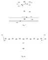
- FIG. 3is a circuit diagram showing a biasing scheme for programming selected cell S while avoiding inadvertent programming of half-selected cells H and F and unselected cell U in a cross-point array.
- FIG. 4is a circuit diagram showing voltages across the selected cell S, half-selected cells H and F, and unselected cell U at reduced programming voltage in a cross-point array.
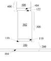
- FIG. 5is a cross-sectional view of a memory cell formed according to a preferred embodiment of the present invention.
- FIG. 6is a cross-sectional view of a memory cell formed according to an alternative embodiment of the present invention.
- FIG. 7is a cross-sectional view of a memory cell formed according to another alternative embodiment of the present invention.
- FIGS. 8 a - 8 care cross-sectional views showing stages in formation of a first memory level of a monolithic three dimensional memory array formed according to a preferred embodiment of the present invention.
- FIG. 1shows an embodiment of a memory cell described in Herner et al., U.S. Pat. No. 6,952,030, “High-density three-dimensional memory cell,” hereinafter the '030 patent.
- pillar 300comprising a diode 302 and a dielectric rupture antifuse 118 , are arranged electrically in series between top conductor 400 and bottom conductor 200 .
- pillar 300comprising a diode 302 and a dielectric rupture antifuse 118
- FIG. 1shows an embodiment of a memory cell described in Herner et al., U.S. Pat. No. 6,952,030, “High-density three-dimensional memory cell,” hereinafter the '030 patent.
- pillar 300comprising a diode 302 and a dielectric rupture antifuse 118 , are arranged electrically in series between top conductor 400 and bottom conductor 200 .
- Application of a relatively large programming currentpermanently alters the memory cell of FIG. 1 so
- diode 302is formed of semiconductor material which, in the initial, unprogrammed device, is in a relatively high-resistivity state. Application of a programming voltage across diode 302 changes the semiconductor material from a high-resistivity state to a lower-resistivity state.
- the programming voltagemust perform two tasks. It must convert the semiconductor material of diode 302 from a high-resistivity to a low-resistivity state, and must also cause the dielectric material of dielectric rupture antifuse 118 to undergo dielectric breakdown, during which at least one conductive path is permanently formed through dielectric rupture antifuse 118 .
- FIG. 2shows a portion of a first memory level of cells like those of FIG. 1 arranged in a cross-point array comprising a plurality of memory cells.
- Each memory cellcomprises a pillar 300 (which comprises the diode 302 and antifuse 118 shown in FIG. 1 ), disposed between one of top conductors 400 and one of bottom conductors 200 .
- Top conductors 400are above bottom conductors 200 and extend in a different direction, preferably perpendicular to them. Two, three, or more such memory levels can be vertically stacked atop one another, forming a monolithic three dimensional memory array.
- FIG. 3illustrates a biasing scheme that may be used to program a memory cell in a cross-point memory array like that shown in FIG. 2 .
- selected cell Sis to be subjected to a programming voltage of 10 volts (the voltages supplied here are examples only).
- Selected bitline B 0is set at 10 volts and selected wordline W 0 at 0 volts, placing 10 volts across selected cell S.
- unselected wordline W 1is set to 9 volts; thus cell F is subjected to only 1 volt, which is below the turn-on voltage for the diode.
- unselected bitline B 1is set to 1 volt; thus cell H, which shares wordline W 0 with selected cell S, is subjected to only 1 volt.
- Unselected cell Uwhich shares neither wordline nor bitline with selected cell S, is subjected to ⁇ 8 volts. Note that in this simplified figure, only one unselected bitline B 1 and only one unselected wordline W 1 are shown. In reality there will be many unselected wordlines and bitlines.
- An array with N bitlines and M wordlineswill include N ⁇ 1 F cells, M ⁇ 1 H cells, and a very large number (N ⁇ 1)*(M ⁇ 1) of U cells.
- the diode in each of the U cellsis under reverse bias at a voltage below the diode's breakdown voltage, minimizing the current that flows through this cell. (A diode conducts current asymmetrically, conducting current more readily in one direction than in the other.) There will inevitably be some reverse leakage current, however, and due to the large number of U cells, the reverse leakage current during programming of the selected cell may waste significant power. During programming of the selected cell S, the forward current on H cells and F cells that have been programmed, though small, similarly wastes power. High programming voltage itself is often difficult to generate. For all of these reasons, it is desirable to minimize the magnitude of the electrical pulse required to program the selected memory cell in such a cross-point memory array.
- Feature sizeis the smallest feature that can be formed by a photolithographic process. Note that for horizontally oriented devices such as transistors, as feature size decreases, in general voltages required to operate the device also decrease. In the memory cell of FIG. 1 , however, because of the vertical orientation of the memory cell, in general the magnitude of electrical pulse required to transform the semiconductor material of the diode and to rupture the antifuse does not decrease with features size.
- a dielectric rupture antifuseis paired with a semiconductor diode formed of semiconductor material, for example silicon, where the semiconductor material of the diode is in a low-resistivity state as formed, and need not be converted.
- the diode of the '030 patent and the '549 applicationis formed by depositing a semiconductor material such as silicon in an amorphous state, then performing a thermal anneal to crystallize the silicon, forming a polycrystalline silicon or polysilicon diode.
- a semiconductor materialsuch as silicon in an amorphous state
- a thermal annealto crystallize the silicon
- the polysiliconforms with a high number of crystalline defects, causing it to be high-resistivity.
- Application of a programming pulse through this high-defect polysiliconapparently alters the polysilicon, causing it to be lower-resistivity.
- a memory cellBy pairing a dielectric rupture antifuse with such a low-defect, low-resistivity diode, a memory cell can be formed in which the programming pulse need only be sufficient to rupture the dielectric rupture antifuse; the diode is formed of semiconductor material which in its initial state is already low-resistivity and does not need to undergo a high-resistivity-to-low-resistivity conversion.
- the low-defect diodeis paired with a dielectric rupture antifuse formed of a conventional dielectric material, silicon dioxide.
- the dielectric rupture antifuse in such a devicemust be thick enough to be reliably insulating, requiring a relatively large programming voltage. This programming voltage can be reduced by reducing the thickness of the silicon dioxide antifuse. As the silicon dioxide antifuse gets thinner, however, it becomes more vulnerable to defects, which will allow for unwanted leakage current.
- the silicon dioxide layer which serves as an antifuseis generally thermally grown.
- the quality of the antifusecan be improved, and defects decreased, by growing the antifuse at a higher temperature, for example 1000 degrees C.
- High temperaturehas other disadvantages, however, causing unwanted diffusion of dopants in diodes and in CMOS control circuits formed beneath the memory levels, damaging and potentially ruining those devices.
- a materialhas a characteristic dielectric constant k.
- the dielectric constant of a materialdescribes its behavior as an insulator.
- a good insulatorsuch as conventionally formed silicon dioxide has a low dielectric constant of 3.9.
- a vacuumby definition, has the lowest possible dielectric constant of 1.
- a range of materials, including, for example, HfO 2 and Al 2 O 3are considered dielectrics, yet have dielectric constants higher than that of silicon dioxide.
- a layer of a higher-k material, such as HfO 2 or Al 2 O 3 , serving as a dielectric rupture antifusecan be thicker than a layer of a lower-k material such as silicon dioxide of comparable quality while having the same electrical behavior.
- McPherson et al.in “Proposed universal relationship between dielectric breakdown and dielectric constant,” Proceedings of 2002 IEDM, pp. 633-636, demonstrate that materials having higher dielectric constant k undergo dielectric breakdown at lower electric fields than lower dielectric constant materials. For reasons described earlier, it is desirable to reduce programming voltage in a memory array.
- a diode formed of low-defect deposited semiconductor material crystallized adjacent to a silicideis paired with a dielectric rupture antifuse formed of a high-k material, having a dielectric constant k greater than about 8.
- deposited semiconductor materialrefers to semiconductor materials such as silicon, germanium, or silicon-germanium alloys that have been deposited, and excludes the monocrystalline wafer substrate above which the device may be built.
- the voltage required to program the cellis only that required to rupture the antifuse by subjecting it to dielectric breakdown. Forming the antifuse of a high-k material serves to reduce programming voltage while maintaining a highly reliable antifuse before programming with low leakage current after programming.
- gate oxides of transistorshave been investigated for use in gate oxides of transistors because they can be made thicker than gate oxides of, say, silicon dioxide while having the same or better capacitance. These gate oxides serve a different role in the transistor, however, than the antifuse described here. These gate oxides are not intended, at any point in the life of the device, to suffer dielectric breakdown.
- atomic layer depositionis used to form the dielectric rupture antifuse of a high-k material.
- ALDatomic layer deposition
- Recent advances in ALD techniqueshave allowed an extremely high-quality layer of high-k material to be formed which is very thin, for example 50, 30, 20, or 10 angstroms, or less. This very thin layer is of such high quality that leakage current is acceptably low, and such a thin layer requires lower voltage to break down.
- McPherson et al.describe that higher-k dielectrics have the additional advantage that they tend to exhibit more uniform breakdown behavior than lower-k dielectrics such as silicon dioxide.
- the programming voltagemust be high enough to rupture antifuses at the high end of the distribution, even though a lower voltage will suffice for most memory cells in the array. A tighter distribution allows further decrease in programming voltage.
- high-k dielectricscan be formed at relatively low temperature by various deposition processes, including ALD.
- ALDatomic layer deposition
- a diodeconducts current asymmetrically, conducting more readily under forward bias than under reverse bias.
- Reverse leakage currentthe current that flows under reverse bias, is undesirable.
- Reverse leakage currentreduces superlinearly with reduced negative voltage across the diode.
- the reverse leakage currentwhen the diode was under ⁇ 7 volts, the reverse leakage current was ⁇ 7.5 ⁇ 10 ⁇ 11 amps.
- voltagewas ⁇ 5.5 volts, the reverse leakage current was substantially reduced to ⁇ 3.0 ⁇ 10 ⁇ 11 amps. Under voltage of ⁇ 4.5 volts, reverse leakage current was reduced to 1.6 ⁇ 10 ⁇ 11 amps.
- siliconhas generally been preferred to form the diode.
- Germaniumhas a smaller band gap than silicon, and it has been found that a diode formed of an alloy of silicon and germanium has higher reverse leakage current than a pure silicon diode.
- the leakage currentincreases with the fraction of germanium.
- unselected cells Uat only ⁇ 3.4 volts, the leakage current will be substantially less, mitigating this disadvantage.
- FIG. 5shows a memory cell formed according to a preferred embodiment of the present invention.
- Bottom conductor 200includes adhesion layer 104 , preferably of titanium nitride, and conductive layer 106 , preferably of tungsten.
- a dielectric rupture antifuse 118 formed of a high-k dielectric materialis formed above bottom conductor 200 .
- a barrier layer 110for example of titanium nitride, intervenes between dielectric rupture antifuse 118 and vertically oriented contiguous p-i-n diode 302 . Layer 110 may be omitted in some embodiments.
- Pillar 300includes barrier layer 110 and diode 302 .
- Silicide layer 122which is preferably cobalt silicide or titanium silicide, is part of top conductor 400 , which further includes conductive layers such as, for example, titanium nitride layer 404 and tungsten layer 406 .
- conductive layerssuch as, for example, titanium nitride layer 404 and tungsten layer 406 .
- silicideis only formed where a silicide-forming metal is in contact with the silicon of diode 302 ; the cross-hatched portion of layer 122 is unreacted metal, not silicide.
- Top conductor 400which is shown slightly misaligned with underlying pillar 300 , is preferably rail-shaped, shown in cross-section extending out of the page.
- Preferred materials for use in antifuse 118include HfO 2 , Al 2 O 3 , ZrO 2 , TiO 2 , La 2 O 3 , Ta 2 O 5 , RuO 2 , ZrSiO x , AlSiO x , HfSiO x , HfAlO x , HfSiON, ZrSiAlO x , HfSiAlO x , HfSiAlON, and ZrSiAlON.
- the silicon of diode 302is preferably deposited amorphous, then crystallized. In some embodiments, it may be preferred to crystallize diode 302 , then strip silicide 122 so it is not present in the finished device. Additional layers which are not shown may be present, such as barrier layers and adhesion layers; alternatively, some barrier layers which are included may be omitted in some embodiments.
- FIG. 6shows an alternative embodiment.
- Bottom conductor 200is formed as in the embodiment of FIG. 5 .
- Pillar 300includes barrier layer 110 (preferably titanium nitride), contiguous p-i-n diode 302 , silicide layer 122 , conductive barrier layer 123 , dielectric rupture antifuse 118 formed of a high-k dielectric material, and conductive barrier layer 125 .
- Top conductor 400includes conductive adhesion layer 404 , preferably of titanium nitride, and conductive layer 406 , for example of tungsten.
- FIG. 7shows another alternative embodiment.
- Bottom conductor 200is formed as in the embodiments of FIGS. 5 and 6 .
- Pillar 300includes barrier layer 110 (preferably titanium nitride) and contiguous p-i-n diode 302 .
- Short pillar 304etched in a different etch step from pillar 300 , includes silicide layer 122 and conductive barrier layer 123 .
- Top conductor 400includes conductive adhesion layer 402 , preferably of titanium nitride, and conductive layer 406 , for example of tungsten.
- Dielectric rupture antifuse 118formed of a high-k dielectric material intervenes between top conductor 400 and conductive barrier layer 123 . It can be a continuous blanket, or can be patterned with top conductor 400 , as shown. Many other alternative embodiments can be imagined which similarly include a contiguous p-i-n diode and a high-k dielectric rupture antifuse.
- Each of these embodimentsis a semiconductor device comprising: a contiguous p-i-n diode formed of deposited semiconductor material, wherein the semiconductor material was crystallized adjacent to a silicide, germanide, or silicide-germanide layer; and a dielectric rupture antifuse arranged electrically in series with the diode, the dielectric rupture antifuse comprising a dielectric material having a dielectric constant greater than 8.
- the vertically oriented diodeis disposed between a bottom conductor and a top conductor
- the dielectric rupture antifuseis disposed between the diode and the top conductor or between the diode and the bottom conductor.
- neither the top nor the bottom conductorcomprises a silicon layer.
- contiguous p-i-n diodedescribes a diode formed of semiconductor material which has heavily doped p-type semiconductor material at one end and heavily doped n-type semiconductor material at the other, with intrinsic or lightly doped semiconductor material between, with no dielectric rupture antifuse sufficient to prevent most current flow before it is ruptured intervening between the p-type region and the n-type region.
- a p-i-n diodeis preferred for use in a large memory array because such a diode minimizes leakage current under reverse bias.
- the antifuse 118is intact and impedes current flow.
- a portion of the dielectric rupture antifusesuffers dielectric breakdown, forming a conductive path through the dielectric rupture antifuse 118 between the contiguous p-i-n diode 302 and the top conductor 400 or between the contiguous p-i-n diode 302 and the bottom conductor 200 .
- the dielectric rupture antifuse formed of a high-k dielectric materialmay be disposed between two metal or metallic layers such as titanium nitride or a conductive metal silicide. These conductive layers help build capacitance across the antifuse, allowing it to rupture more readily than if the antifuse is disposed between semiconductor layers or between a semiconductor layer and a metal or metallic layer.
- This substrate 100can be any semiconducting substrate known in the art, such as monocrystalline silicon, IV-IV compounds like silicon-germanium or silicon-germanium-carbon, III-V compounds, II-VII compounds, epitaxial layers over such substrates, or any other semiconducting material.
- the substratemay include integrated circuits fabricated therein.
- the insulating layer 102is formed over substrate 100 .
- the insulating layer 102can be silicon oxide, silicon nitride, Si—C—O—H film, or any other suitable insulating material.
- the first conductors 200are formed over the substrate 100 and insulator 102 .
- An adhesion layer 104may be included between the insulating layer 102 and the conducting layer 106 to help conducting layer 106 adhere to insulating layer 102 . If the overlying conducting layer 106 is tungsten, titanium nitride is preferred as adhesion layer 104 .
- Conducting layer 106can comprise any conducting material known in the art, such as tungsten, or other materials, including tantalum, titanium, copper, cobalt, or alloys thereof.
- the layerswill be patterned and etched using any suitable masking and etching process to form substantially parallel, substantially coplanar conductors 200 , shown in FIG. 8 a in cross-section.
- Conductors 200extend out of the page.
- photoresistis deposited, patterned by photolithography and the layers etched, and then the photoresist removed using standard process techniques.
- Dielectric material 108is deposited over and between conductor rails 200 .
- Dielectric material 108can be any known electrically insulating material, such as silicon oxide, silicon nitride, or silicon oxynitride.
- silicon dioxide deposited by a high-density plasma methodis used as dielectric material 108 .
- dielectric material 108 on top of conductor rails 200is removed, exposing the tops of conductor rails 200 separated by dielectric material 108 , and leaving a substantially planar surface.
- the resulting structureis shown in FIG. 8 a.
- This removal of dielectric overfill to form the planar surfacecan be performed by any process known in the art, such as chemical mechanical planarization (CMP) or etchback.
- CMPchemical mechanical planarization
- conductors 200could be formed by a Damascene method instead.
- a thin layer 118 of a high-k dielectric materialhaving a dielectric constant k greater than about 8, is formed.
- the value of dielectric constant k for this materialis preferably between 8 and 50, most preferably between about 8 and about 25.
- This layeris preferably between about 10 and about 200 angstroms, for example between about 20 and about 100 angstroms.
- Preferred materials for layer 118include HfO 2 , Al 2 O 3 , ZrO 2 , TiO 2 , La 2 O 3 , Ta 2 O 5 , RuO 2 , ZrSiO x , AlSiO x , HfSiO x , HfAlO x , HfSiON, ZrSiAlO x , HfSiAlO x , HfSiAlON, and ZrSiAlON. In some embodiments two or more of these materials may be blended. Most preferred materials include HfO 2 , which has a dielectric constant of about 25, or Al 2 O 3 , which has a dielectric constant of about 9.
- layer 118is formed by ALD, forming a very high-quality film.
- a high-quality filmis preferably dense, as close to its theoretical density as possible; has complete coverage with few or no pinholes; and has a low density of electrical defects.
- materials of comparable film quality having a higher dielectric constantto be thicker than those with a lower dielectric constant.
- a film of Al 2 O 3 formed by ALDpreferably has a thickness between about 5 and about 80 angstroms, preferably about 30 angstroms, while a film of HfO 2 formed by ALD preferably has a thickness between about 5 and about 100 angstroms, preferably about 40 angstroms.
- Layer 118will serve as a dielectric rupture antifuse.
- a conductive barrier layer(not shown) before depositing layer 118 .
- This barrier layerfor example of about 100 angstroms of titanium nitride, will provide a uniform surface on which to deposit high-k dielectric rupture antifuse layer 118 , which may improve the uniformity of that layer.
- Barrier layer 111is deposited on layer 118 . It can be any appropriate conductive barrier material, for example titanium nitride, with any appropriate thickness, for example 50 to 200 angstroms, preferably 100 angstroms. In some embodiments barrier layer 111 may be omitted.
- the semiconductor materialcan be silicon, germanium, a silicon-germanium alloy, or other suitable semiconductors, or semiconductor alloy.
- silicongermanium
- a silicon-germanium alloyor other suitable semiconductors, or semiconductor alloy.
- this descriptionwill refer to the semiconductor material as silicon, but it will be understood that the skilled practitioner may select any of these other suitable materials instead.
- Bottom heavily doped region 112can be formed by any deposition and doping method known in the art.
- the siliconcan be deposited and then doped, but is preferably doped in situ by flowing a donor gas providing n-type dopant atoms, for example phosphorus, during deposition of the silicon.
- Heavily doped region 112is preferably between about 100 and about 800 angstroms thick.
- Intrinsic region 114can be formed by any method known in the art. Region 114 can be silicon, germanium, or any alloy of silicon or germanium and has a thickness between about 1100 and about 3300 angstroms, preferably about 2000 angstroms. The silicon of heavily doped region 112 and intrinsic region 114 is preferably amorphous as deposited.
- Pillars 300should have about the same pitch and about the same width as conductors 200 below, such that each pillar 300 is formed on top of a conductor 200 . Some misalignment can be tolerated.
- Pillars 300can be formed using any suitable masking and etching process.
- photoresistcan be deposited, patterned using standard photolithography techniques, and etched, then the photoresist removed.
- a hard mask of some other materialfor example silicon dioxide, can be formed on top of the semiconductor layer stack, with bottom antireflective coating (BARC) on top, then patterned and etched.
- BARCbottom antireflective coating
- DARCdielectric antireflective coating
- Dielectric material 108is deposited over and between the semiconductor pillars 300 , filling the gaps between them.
- Dielectric material 108can be any known electrically insulating material, such as silicon oxide, silicon nitride, or silicon oxynitride. In a preferred embodiment, silicon dioxide is used as the insulating material.
- dielectric material on top of pillars 300is removed, exposing the tops of pillars 300 separated by dielectric material 108 , and leaving a substantially planar surface.
- This removal of dielectric overfillcan be performed by any process known in the art, such as CMP or etchback.
- CMP or etchbackion implantation is performed, forming heavily doped p-type top regions 116 .
- the p-type dopantis preferably a shallow implant of boron, with an implant energy of, for example, 2 keV, and dose of about 3 ⁇ 10 15 /cm 2 .
- This implant stepcompletes formation of diodes 302 .
- the resulting structureis shown in FIG. 8 b. In the diodes just formed, bottom heavily doped regions 112 are n-type while top heavily doped regions 116 are p-type; clearly the polarity of the diodes could be reversed.
- the pillars 300are formed by depositing a semiconductor layerstack above the first conductors 200 ; patterning and etching the semiconductor layerstack in the form of pillars 300 in a single patterning step. After completion of the device, the contiguous p-i-n diode is disposed within the pillar.
- a layer 120 of a silicide-forming metalfor example titanium, cobalt, chromium, tantalum, platinum, nickel, niobium, or palladium
- Layer 120is preferably titanium or cobalt; if layer 120 is titanium, its thickness is preferably between about 10 and about 100 angstroms, most preferably about 20 angstroms.
- Layer 120is followed by titanium nitride layer 404 . Both layers 120 and 404 are preferably between about 20 and about 100 angstroms, most preferably about 50 angstroms.
- a layer 406 of a conductive materialfor example tungsten, is deposited. Layers 406 , 404 , and 120 are patterned and etched into rail-shaped top conductors 400 , which preferably extend in a direction perpendicular to bottom conductors 200 .
- the dielectric materialcan be any known electrically insulating material, such as silicon oxide, silicon nitride, or silicon oxynitride. In a preferred embodiment, silicon oxide is used as this dielectric material.
- Formation of a first memory levelhas been described. Additional memory levels can be formed above this first memory level to form a monolithic three dimensional memory array.
- the array just describedis just one example; and may vary in other ways, for example including either of the memory cells shown in FIGS. 6 and 7 .
- layer 120 of a silicide-forming metalis in contact with the silicon of top heavily doped region 116 .
- the metal of layer 120will react with some portion of the silicon of heavily doped region 116 to form a silicide layer (not shown).
- This silicide layerforms at a temperature lower than the temperature required to crystallize silicon, and thus will form while regions 112 , 114 , and 116 are still largely amorphous.
- a silicide-germanide layermay form, for example of cobalt silicide-germanide or titanium silicide-germanide.
- a single crystallizing annealis performed to crystallize diodes 302 , for example at 750 degrees C. for about 60 seconds, though each memory level can be annealed as it is formed.
- the resulting diodeswill generally be polycrystalline. Since the semiconductor material of these diodes is crystallized in contact with a silicide or silicide-germanide layer with which it has a good lattice match, the semiconductor material of diodes 302 will be low-defect and low-resistivity.
- HfO 2was used for dielectric rupture antifuse 118 , care should be taken to keep processing temperatures below the crystallization temperature of HfO2, which may be about 700 to about 800 degrees C.
- An intact antifuse layer of crystalline HfO 2has much higher leakage than a layer of amorphous HfO 2 .
- conductorscan be shared between memory levels; i.e. top conductor 400 would serve as the bottom conductor of the next memory level above.
- an interlevel dielectric(not shown) is formed above the first memory level of FIG. 8 c, its surface planarized, and construction of a second memory level begins on this planarized interlevel dielectric, with no shared conductors.
- a programming voltage sufficient to program more nearly all (more than 99 percent, for example) of the cells in an arrayincludes a pulse across the cell to be programmed of at least 8 volts.
- programming voltagecan be reduced.
- nearly all of the cells in an arraycan be programmed with a programming pulse less than about 8 volts, and in some embodiments less than 6 volts, or less than 4.0 volts.
- the programming pulsemay be applied with the diode in reverse bias. This may have advantages in reducing or eliminating leakage across the unselected cells in the array, as described in Kumar et al., U.S. patent application Ser. No. 11/496,986, “Method For Using A Memory Cell Comprising Switchable Semiconductor Memory Element With Trimmable Resistance,” filed Jul. 28, 2006, owned by the assignee of the present invention and hereby incorporated by reference.
- a monolithic three dimensional memory arrayis one in which multiple memory levels are formed above a single substrate, such as a wafer, with no intervening substrates.
- the layers forming one memory levelare deposited or grown directly over the layers of an existing level or levels.
- stacked memorieshave been constructed by forming memory levels on separate substrates and adhering the memory levels atop each other, as in Leedy, U.S. Pat. No. 5,915,167, “Three dimensional structure memory.”
- the substratesmay be thinned or removed from the memory levels before bonding, but as the memory levels are initially formed over separate substrates, such memories are not true monolithic three dimensional memory arrays.
- a monolithic three dimensional memory array formed above a substratecomprises at least a first memory level formed at a first height above the substrate and a second memory level formed at a second height different from the first height. Three, four, eight, or indeed any number of memory levels can be formed above the substrate in such a multilevel array.
Landscapes
- Physics & Mathematics (AREA)
- Condensed Matter Physics & Semiconductors (AREA)
- General Physics & Mathematics (AREA)
- Engineering & Computer Science (AREA)
- Computer Hardware Design (AREA)
- Microelectronics & Electronic Packaging (AREA)
- Power Engineering (AREA)
- Semiconductor Memories (AREA)
Abstract
Description
- This application is a continuation-in-part of Herner, U.S. patent application Ser. No. 10/954,510, “Memory Cell Comprising a Semiconductor Junction Diode Crystallized Adjacent to a Silicide,” filed Sep. 29, 2004, hereinafter the '510 application, which is a continuation-in-part of Petti et al., U.S. Pat. No. 6,946,719, “Semiconductor Device Including Junction Diode Contacting Contact-Antifuse Unit Comprising Silicide,” both owned by the assignee of the present invention and both hereby incorporated by reference. This application is related to Herner, U.S. patent application Ser. No. ______ “Method for Making a P-I-N Diode Crystallized Adjacent to a Silicide in Series with a Dielectric Antifuse,” filed on even date herewith and hereby incorporated by reference in its entirety.
- The invention relates to a nonvolatile memory cell including a diode and a dielectric rupture antifuse formed electrically in series between conductors. In general, it is advantageous to minimize the voltage required to program such a memory cell.
- The present invention is defined by the following claims, and nothing in this section should be taken as a limitation on those claims. In general, the invention is directed to a nonvolatile memory cell including a dielectric rupture antifuse formed of high-dielectric constant-antifuse material and a semiconductor diode formed of low-resistivity semiconductor material.
- A first aspect of the invention provides for a method for forming and programming a nonvolatile memory cell, the method comprising: forming a contiguous p-i-n diode, the contiguous p-i-n diode comprising deposited semiconductor material; forming a layer of a silicide, silicide-germanide, or germanide in contact with the deposited semiconductor material; crystallizing the deposited semiconductor material in contact with the layer of silicide, silicide-germanide, or germanide; forming a layer of a dielectric material having a dielectric constant greater than 8; and subjecting a portion of the layer of dielectric material to dielectric breakdown, wherein the memory cell comprises the contiguous p-i-n diode and the layer of dielectric material.
- Another aspect of the invention provides for a first memory level comprising: a plurality of first substantially parallel, substantially coplanar conductors formed above a substrate; a plurality of second substantially parallel, substantially coplanar conductors formed above the first conductors; a plurality of vertically oriented contiguous p-i-n diodes comprising semiconductor material, the semiconductor material crystallized adjacent to a silicide, silicide-germanide, or germanide layer; a plurality of dielectric rupture antifuses formed of a dielectric material having a dielectric constant greater than about 8, wherein each of the contiguous p-i-n diodes is disposed between one of the first conductors and one of the second conductors, and wherein each of the dielectric rupture antifuses is disposed between one of the first conductors and one of the contiguous p-i-n diodes or between one of the second conductors and one of the contiguous p-i-n diodes; and a plurality of memory cells, each memory cell comprising one of the contiguous p-i-n diodes and one of the dielectric rupture antifuses.
- A preferred embodiment of the invention provides for a monolithic three dimensional memory array formed above a substrate comprising: a) a first memory level monolithically formed above the substrate, the first memory level comprising: i) a plurality of first substantially parallel, substantially coplanar conductors extending in a first direction; ii) a plurality of second substantially parallel, substantially coplanar conductor extending in a second direction different from the first direction, the second conductors above the first conductors; iii) a plurality of vertically oriented contiguous p-i-n diodes formed of deposited semiconductor material, the semiconductor material crystallized adjacent to a silicide, silicide-germanide, or germanide layer, each diode vertically disposed between one of the first conductors and one of the second conductors; iv) a plurality of dielectric rupture antifuses formed of a dielectric material having a dielectric constant greater than 8; and v) a plurality of memory cells, each memory cell comprising one of the diodes and one of the dielectric rupture antifuses arranged in series; and b) a second memory level monolithically formed above the first memory level.
- Another aspect of the invention provides for a device comprising: a contiguous p-i-n diode comprising semiconductor material; a silicide or silicide-germanide layer in contact with the semiconductor material of the contiguous p-i-n diode; and a dielectric rupture antifuse comprising a dielectric material, the dielectric material having a dielectric constant of8 or greater, wherein the contiguous p-i-n diode and the dielectric rupture antifuse are arranged electrically in series between a first conductor and a second conductor.
- Still another aspect of the invention provides for a method for forming and programming a nonvolatile memory cell, the method comprising: forming a contiguous p-i-n diode, the contiguous p-i-n diode comprising deposited semiconductor material; forming a layer of a silicide, silicide-germanide, or germanide in contact with the deposited semiconductor material; crystallizing the deposited semiconductor material in contact with the layer of silicide, silicide-germanide, or germanide; forming a layer of a dielectric material having a dielectric constant greater than 8; and subjecting a portion of the layer of dielectric material to dielectric breakdown, wherein the memory cell comprises the contiguous p-i-n diode and the layer of dielectric material.
- An additional aspect of the invention provides for a method for monolithically forming a first memory level above a substrate, the method comprising: forming a plurality of first substantially parallel, substantially coplanar conductors above the substrate, the first conductors extending in a first direction; forming a plurality of vertically oriented contiguous p-i-n diodes above the first conductors, the contiguous p-i-n diode comprising semiconductor material crystallized in contact with a silicide, silicide-germanide, or germanide layer; forming a plurality of second substantially parallel, substantially coplanar conductors, the second conductors above the contiguous p-i-n diodes, the second conductors extending in a second direction different from the first direction, each contiguous p-i-n diode vertically disposed between one of the first conductors and one of the second conductors; and forming a plurality of dielectric rupture antifuses, each dielectric rupture antifuse disposed between one of the contiguous p-i-n diodes and one of the first conductors or between one of the contiguous p-i-n diodes and one of the second conductors, wherein the dielectric rupture antifuses comprise dielectric material, the dielectric material having a dielectric constant greater than about 8.
- A preferred embodiment of the invention provides for a method for forming a monolithic three dimensional memory array above a substrate, the method comprising: a) monolithically forming a first memory level above the substrate, the first memory level formed by a method comprising: i) forming a plurality of first substantially parallel, substantially coplanar conductors extending in a first direction; ii) forming a plurality of second substantially parallel, substantially coplanar conductor extending in a second direction different from the first direction, the second conductors above the first conductors; iii) forming a plurality of vertically oriented contiguous p-i-n diodes formed of deposited semiconductor material, the deposited semiconductor material crystallized in contact with a silicide, silicide-germanide, or germanide layer, each diode vertically disposed between one of the first conductors and one of the second conductors; iv) forming a plurality of dielectric rupture antifuses formed of a dielectric material having a dielectric constant greater than 8; and v) forming a plurality of memory cells, each memory cell comprising one of the diodes and one of the dielectric rupture antifuses arranged in series; and b) monolithically forming a second memory level above the first memory level.
- Each of the aspects and embodiments of the invention described herein can be used alone or in combination with one another.
- The preferred aspects and embodiments will now be described with reference to the attached drawings.
FIG. 1 is a perspective view of the memory cell of U.S. Pat. No. 6,952,030.FIG. 2 is a perspective view of a memory level comprising memory cells.FIG. 3 is a circuit diagram showing a biasing scheme for programming selected cell S while avoiding inadvertent programming of half-selected cells H and F and unselected cell U in a cross-point array.FIG. 4 is a circuit diagram showing voltages across the selected cell S, half-selected cells H and F, and unselected cell U at reduced programming voltage in a cross-point array.FIG. 5 is a cross-sectional view of a memory cell formed according to a preferred embodiment of the present invention.FIG. 6 is a cross-sectional view of a memory cell formed according to an alternative embodiment of the present invention.FIG. 7 is a cross-sectional view of a memory cell formed according to another alternative embodiment of the present invention.FIGS. 8 a-8care cross-sectional views showing stages in formation of a first memory level of a monolithic three dimensional memory array formed according to a preferred embodiment of the present invention.FIG. 1 shows an embodiment of a memory cell described in Herner et al., U.S. Pat. No. 6,952,030, “High-density three-dimensional memory cell,” hereinafter the '030 patent. In this nonvolatile memory cell,pillar 300, comprising adiode 302 and adielectric rupture antifuse 118, are arranged electrically in series betweentop conductor 400 andbottom conductor 200. In the initial state of this memory cell, when a read voltage is applied betweentop conductor 400 andbottom conductor 200 very little current flows between them. Application of a relatively large programming current permanently alters the memory cell ofFIG. 1 so that, after programming, much more current flows at the same read voltage. This difference in current under the same applied read voltage allows a programmed cell to be distinguished from an unprogrammed cell; for example for a data “0” to be distinguished from a data “1”.- As described in detail in Herner et al., U.S. patent application Ser. No. 10/955,549, “Nonvolatile Memory Cell Without a Dielectric Antifuse Having High- and Low-Impedance States,” filed Sep. 29, 2004 and hereinafter the '549 application; and in Herner et al., U.S. patent application Ser. No. 11/148,530, “Nonvolatile Memory Cell Operating by Increasing Order in Polycrystalline Semiconductor Material,” filed Jun. 8, 2005, and hereinafter the '530 application, both owned by the assignee of the present invention and hereby incorporated by reference,
diode 302 is formed of semiconductor material which, in the initial, unprogrammed device, is in a relatively high-resistivity state. Application of a programming voltage acrossdiode 302 changes the semiconductor material from a high-resistivity state to a lower-resistivity state. - In a cell like that shown in
FIG. 1 , the programming voltage must perform two tasks. It must convert the semiconductor material ofdiode 302 from a high-resistivity to a low-resistivity state, and must also cause the dielectric material ofdielectric rupture antifuse 118 to undergo dielectric breakdown, during which at least one conductive path is permanently formed throughdielectric rupture antifuse 118. FIG. 2 shows a portion of a first memory level of cells like those ofFIG. 1 arranged in a cross-point array comprising a plurality of memory cells. Each memory cell comprises a pillar300 (which comprises thediode 302 andantifuse 118 shown inFIG. 1 ), disposed between one oftop conductors 400 and one ofbottom conductors 200.Top conductors 400 are abovebottom conductors 200 and extend in a different direction, preferably perpendicular to them. Two, three, or more such memory levels can be vertically stacked atop one another, forming a monolithic three dimensional memory array.FIG. 3 illustrates a biasing scheme that may be used to program a memory cell in a cross-point memory array like that shown inFIG. 2 . Suppose selected cell S is to be subjected to a programming voltage of10 volts (the voltages supplied here are examples only). Selected bitline B0 is set at 10 volts and selected wordline W0 at 0 volts, placing 10 volts across selected cell S. To avoid inadvertent programming of cell F, which shares bitline B0 with selected cell S, unselected wordline W1 is set to 9 volts; thus cell F is subjected to only 1 volt, which is below the turn-on voltage for the diode. Similarly, unselected bitline B1 is set to 1 volt; thus cell H, which shares wordline W0 with selected cell S, is subjected to only 1 volt. Unselected cell U, which shares neither wordline nor bitline with selected cell S, is subjected to −8 volts. Note that in this simplified figure, only one unselected bitline B1 and only one unselected wordline W1 are shown. In reality there will be many unselected wordlines and bitlines. An array with N bitlines and M wordlines will include N−1 F cells, M−1 H cells, and a very large number (N−1)*(M−1) of U cells.- The diode in each of the U cells is under reverse bias at a voltage below the diode's breakdown voltage, minimizing the current that flows through this cell. (A diode conducts current asymmetrically, conducting current more readily in one direction than in the other.) There will inevitably be some reverse leakage current, however, and due to the large number of U cells, the reverse leakage current during programming of the selected cell may waste significant power. During programming of the selected cell S, the forward current on H cells and F cells that have been programmed, though small, similarly wastes power. High programming voltage itself is often difficult to generate. For all of these reasons, it is desirable to minimize the magnitude of the electrical pulse required to program the selected memory cell in such a cross-point memory array.
- Feature size is the smallest feature that can be formed by a photolithographic process. Note that for horizontally oriented devices such as transistors, as feature size decreases, in general voltages required to operate the device also decrease. In the memory cell of
FIG. 1 , however, because of the vertical orientation of the memory cell, in general the magnitude of electrical pulse required to transform the semiconductor material of the diode and to rupture the antifuse does not decrease with features size. - In the '510 application, a dielectric rupture antifuse is paired with a semiconductor diode formed of semiconductor material, for example silicon, where the semiconductor material of the diode is in a low-resistivity state as formed, and need not be converted.
- The diode of the '030 patent and the '549 application is formed by depositing a semiconductor material such as silicon in an amorphous state, then performing a thermal anneal to crystallize the silicon, forming a polycrystalline silicon or polysilicon diode. As described in the '530 application, when deposited amorphous silicon is crystallized in contact solely with materials with which it has a high lattice mismatch, such as silicon dioxide and titanium nitride, the polysilicon forms with a high number of crystalline defects, causing it to be high-resistivity. Application of a programming pulse through this high-defect polysilicon apparently alters the polysilicon, causing it to be lower-resistivity.
- It has been found, however, that when deposited amorphous silicon is crystallized in contact with a layer of an appropriate silicide, for example titanium silicide or cobalt silicide, the resulting crystallized silicon is much higher quality, with fewer defects, and has much lower resistivity. The lattice spacing of titanium silicide or cobalt silicide is very close to that of silicon, and it is believed that when amorphous silicon is crystallized in contact with a layer of an appropriate silicide at a favorable orientation, the silicide provides a template for crystal growth of silicon, minimizing formation of defects. Unlike the high-defect silicon crystallized adjacent only to materials with which it has a high lattice mismatch, application of a large electrical pulse does not appreciably change the resistivity of this low-defect, low-resistivity silicon crystallized in contact with the silicide layer.
- By pairing a dielectric rupture antifuse with such a low-defect, low-resistivity diode, a memory cell can be formed in which the programming pulse need only be sufficient to rupture the dielectric rupture antifuse; the diode is formed of semiconductor material which in its initial state is already low-resistivity and does not need to undergo a high-resistivity-to-low-resistivity conversion.
- In embodiments of the '510 application, the low-defect diode is paired with a dielectric rupture antifuse formed of a conventional dielectric material, silicon dioxide. The dielectric rupture antifuse in such a device must be thick enough to be reliably insulating, requiring a relatively large programming voltage. This programming voltage can be reduced by reducing the thickness of the silicon dioxide antifuse. As the silicon dioxide antifuse gets thinner, however, it becomes more vulnerable to defects, which will allow for unwanted leakage current.
- The silicon dioxide layer which serves as an antifuse is generally thermally grown. The quality of the antifuse can be improved, and defects decreased, by growing the antifuse at a higher temperature, for example 1000 degrees C. High temperature has other disadvantages, however, causing unwanted diffusion of dopants in diodes and in CMOS control circuits formed beneath the memory levels, damaging and potentially ruining those devices.
- A material has a characteristic dielectric constant k. The dielectric constant of a material describes its behavior as an insulator. A good insulator such as conventionally formed silicon dioxide has a low dielectric constant of 3.9. A vacuum, by definition, has the lowest possible dielectric constant of 1. A range of materials, including, for example, HfO2and Al2O3, are considered dielectrics, yet have dielectric constants higher than that of silicon dioxide.
- A layer of a higher-k material, such as HfO2or Al2O3, serving as a dielectric rupture antifuse can be thicker than a layer of a lower-k material such as silicon dioxide of comparable quality while having the same electrical behavior.
- McPherson et al., in “Proposed universal relationship between dielectric breakdown and dielectric constant,” Proceedings of 2002 IEDM, pp. 633-636, demonstrate that materials having higher dielectric constant k undergo dielectric breakdown at lower electric fields than lower dielectric constant materials. For reasons described earlier, it is desirable to reduce programming voltage in a memory array. In the present invention, a diode formed of low-defect deposited semiconductor material crystallized adjacent to a silicide is paired with a dielectric rupture antifuse formed of a high-k material, having a dielectric constant k greater than about 8. The term “deposited semiconductor material” refers to semiconductor materials such as silicon, germanium, or silicon-germanium alloys that have been deposited, and excludes the monocrystalline wafer substrate above which the device may be built. The voltage required to program the cell is only that required to rupture the antifuse by subjecting it to dielectric breakdown. Forming the antifuse of a high-k material serves to reduce programming voltage while maintaining a highly reliable antifuse before programming with low leakage current after programming.
- Note that high-k dielectric materials have been investigated for use in gate oxides of transistors because they can be made thicker than gate oxides of, say, silicon dioxide while having the same or better capacitance. These gate oxides serve a different role in the transistor, however, than the antifuse described here. These gate oxides are not intended, at any point in the life of the device, to suffer dielectric breakdown.
- In preferred embodiments, atomic layer deposition (ALD) is used to form the dielectric rupture antifuse of a high-k material. Recent advances in ALD techniques have allowed an extremely high-quality layer of high-k material to be formed which is very thin, for example 50, 30, 20, or 10 angstroms, or less. This very thin layer is of such high quality that leakage current is acceptably low, and such a thin layer requires lower voltage to break down.
- McPherson et al. describe that higher-k dielectrics have the additional advantage that they tend to exhibit more uniform breakdown behavior than lower-k dielectrics such as silicon dioxide. When the dielectric rupture antifuses of a memory array rupture across a wide range of programming voltages, the programming voltage must be high enough to rupture antifuses at the high end of the distribution, even though a lower voltage will suffice for most memory cells in the array. A tighter distribution allows further decrease in programming voltage.
- Many high-k dielectrics can be formed at relatively low temperature by various deposition processes, including ALD. As a general rule, reducing processing temperature is always advantageous in fabrication of a complex semiconductor device, minimizing dopant diffusion, peeling, etc.
- A diode conducts current asymmetrically, conducting more readily under forward bias than under reverse bias. Reverse leakage current, the current that flows under reverse bias, is undesirable. Reverse leakage current reduces superlinearly with reduced negative voltage across the diode. For example, in a diode having a feature size of 0.15 microns formed of low-resistivity semiconductor material as in the present invention, when the diode was under −7 volts, the reverse leakage current was −7.5×10⁻¹¹amps. When voltage was −5.5 volts, the reverse leakage current was substantially reduced to −3.0×10⁻¹¹amps. Under voltage of −4.5 volts, reverse leakage current was reduced to 1.6×10⁻¹¹amps. In the cross-point array pictured in
FIG. 2 , recall that lower voltage required to program the selected cell S results in lower negative voltage across unselected cells U. For example, turning toFIG. 4 , suppose the programming voltage on selected cell S need be only 5.4 volts. The voltage on selected bitline B0 is 5 volts, selected wordline W0 is at 0 volts, for 5.4 volts across selected cell S. If unselected bitline B1 is set to 1 volt and unselected wordline W1 is set to 4.4 volts, cells H and F are both subjected to 1 volt. Unselected cell U is subjected −3.4 volts, significantly lower than −8 volts as in the example ofFIG. 3 . - In the monolithic memory arrays so far described, silicon has generally been preferred to form the diode. Germanium has a smaller band gap than silicon, and it has been found that a diode formed of an alloy of silicon and germanium has higher reverse leakage current than a pure silicon diode. The leakage current increases with the fraction of germanium. In a cross-point memory array, with unselected cells U at only −3.4 volts, the leakage current will be substantially less, mitigating this disadvantage. As described in Herner et al., U.S. patent application Ser. No. 11/125,606, “High-Density Nonvolatile Memory Array Fabricated at Low Temperature Comprising Semiconductor Diodes,” filed May 9, 2005, owned by the assignee of the present invention and hereby incorporated by reference and hereinafter the '606 application, the temperature required to deposit and crystallize silicon by conventional methods are generally incompatible with aluminum and copper metallization, which cannot tolerate high temperature. As described in this application, use of silicon-germanium diodes with sufficiently high germanium content lowers overall fabrication temperature, allowing use of these low-resistivity metals, improving device performance.
FIG. 5 shows a memory cell formed according to a preferred embodiment of the present invention.Bottom conductor 200 includesadhesion layer 104, preferably of titanium nitride, andconductive layer 106, preferably of tungsten. A dielectric rupture antifuse118 formed of a high-k dielectric material is formed abovebottom conductor 200. Abarrier layer 110, for example of titanium nitride, intervenes between dielectric rupture antifuse118 and vertically oriented contiguousp-i-n diode 302.Layer 110 may be omitted in some embodiments.Pillar 300 includesbarrier layer 110 anddiode 302.Silicide layer 122, which is preferably cobalt silicide or titanium silicide, is part oftop conductor 400, which further includes conductive layers such as, for example,titanium nitride layer 404 andtungsten layer 406. (As will be seen, silicide is only formed where a silicide-forming metal is in contact with the silicon ofdiode 302; the cross-hatched portion oflayer 122 is unreacted metal, not silicide.)Top conductor 400, which is shown slightly misaligned withunderlying pillar 300, is preferably rail-shaped, shown in cross-section extending out of the page. Preferred materials for use inantifuse 118 include HfO2, Al2O3, ZrO2, TiO2, La2O3, Ta2O5, RuO2, ZrSiOx, AlSiOx, HfSiOx, HfAlOx, HfSiON, ZrSiAlOx, HfSiAlOx, HfSiAlON, and ZrSiAlON. The silicon ofdiode 302 is preferably deposited amorphous, then crystallized. In some embodiments, it may be preferred to crystallizediode 302, then stripsilicide 122 so it is not present in the finished device. Additional layers which are not shown may be present, such as barrier layers and adhesion layers; alternatively, some barrier layers which are included may be omitted in some embodiments.FIG. 6 shows an alternative embodiment.Bottom conductor 200 is formed as in the embodiment ofFIG. 5 .Pillar 300 includes barrier layer110 (preferably titanium nitride), contiguousp-i-n diode 302,silicide layer 122,conductive barrier layer 123, dielectric rupture antifuse118 formed of a high-k dielectric material, andconductive barrier layer 125.Top conductor 400 includesconductive adhesion layer 404, preferably of titanium nitride, andconductive layer 406, for example of tungsten.FIG. 7 shows another alternative embodiment.Bottom conductor 200 is formed as in the embodiments ofFIGS. 5 and 6 .Pillar 300 includes barrier layer110 (preferably titanium nitride) and contiguousp-i-n diode 302. Short pillar304, etched in a different etch step frompillar 300, includessilicide layer 122 andconductive barrier layer 123.Top conductor 400 includes conductive adhesion layer402, preferably of titanium nitride, andconductive layer 406, for example of tungsten. Dielectric rupture antifuse118 formed of a high-k dielectric material intervenes betweentop conductor 400 andconductive barrier layer 123. It can be a continuous blanket, or can be patterned withtop conductor 400, as shown. Many other alternative embodiments can be imagined which similarly include a contiguous p-i-n diode and a high-k dielectric rupture antifuse.- Each of these embodiments is a semiconductor device comprising: a contiguous p-i-n diode formed of deposited semiconductor material, wherein the semiconductor material was crystallized adjacent to a silicide, germanide, or silicide-germanide layer; and a dielectric rupture antifuse arranged electrically in series with the diode, the dielectric rupture antifuse comprising a dielectric material having a dielectric constant greater than 8. In each embodiment, the vertically oriented diode is disposed between a bottom conductor and a top conductor, the dielectric rupture antifuse is disposed between the diode and the top conductor or between the diode and the bottom conductor. In these examples, neither the top nor the bottom conductor comprises a silicon layer.
- The term “contiguous p-i-n diode” describes a diode formed of semiconductor material which has heavily doped p-type semiconductor material at one end and heavily doped n-type semiconductor material at the other, with intrinsic or lightly doped semiconductor material between, with no dielectric rupture antifuse sufficient to prevent most current flow before it is ruptured intervening between the p-type region and the n-type region. A p-i-n diode is preferred for use in a large memory array because such a diode minimizes leakage current under reverse bias.
- In any of these cells, before programming, the
antifuse 118 is intact and impedes current flow. During programming, when a programming voltage is supplied betweentop conductor 400 andbottom conductor 200, a portion of the dielectric rupture antifuse suffers dielectric breakdown, forming a conductive path through the dielectric rupture antifuse118 between the contiguousp-i-n diode 302 and thetop conductor 400 or between the contiguousp-i-n diode 302 and thebottom conductor 200. - In embodiments of the present invention it may be preferred for the dielectric rupture antifuse formed of a high-k dielectric material to be disposed between two metal or metallic layers such as titanium nitride or a conductive metal silicide. These conductive layers help build capacitance across the antifuse, allowing it to rupture more readily than if the antifuse is disposed between semiconductor layers or between a semiconductor layer and a metal or metallic layer.
- A detailed example will be provided of formation of a monolithic three dimensional memory array formed according to a preferred embodiment of the present invention. For completeness, specific process conditions, dimensions, methods, and materials will be provided. It will be understood, however, that such details are not intended to be limiting, and that many of these details can be modified, omitted or augmented while the results still fall within the scope of the invention. For example, some details from the '030 patent, the '549, '530, and '510 applications may be useful. To avoid obscuring the invention, all details from this patent and these applications have not been included, but it will be understood that no relevant teaching is intended to be excluded.
- Turning to
FIG. 8 a,formation of the memory begins with asubstrate 100. Thissubstrate 100 can be any semiconducting substrate known in the art, such as monocrystalline silicon, IV-IV compounds like silicon-germanium or silicon-germanium-carbon, III-V compounds, II-VII compounds, epitaxial layers over such substrates, or any other semiconducting material. The substrate may include integrated circuits fabricated therein. - An insulating
layer 102 is formed oversubstrate 100. The insulatinglayer 102 can be silicon oxide, silicon nitride, Si—C—O—H film, or any other suitable insulating material. - The
first conductors 200 are formed over thesubstrate 100 andinsulator 102. Anadhesion layer 104 may be included between the insulatinglayer 102 and theconducting layer 106 to help conductinglayer 106 adhere to insulatinglayer 102. If theoverlying conducting layer 106 is tungsten, titanium nitride is preferred asadhesion layer 104. Conductinglayer 106 can comprise any conducting material known in the art, such as tungsten, or other materials, including tantalum, titanium, copper, cobalt, or alloys thereof. - Once all the layers that will form the conductor rails have been deposited, the layers will be patterned and etched using any suitable masking and etching process to form substantially parallel, substantially
coplanar conductors 200, shown inFIG. 8 ain cross-section.Conductors 200 extend out of the page. In one embodiment, photoresist is deposited, patterned by photolithography and the layers etched, and then the photoresist removed using standard process techniques. - Next a
dielectric material 108 is deposited over and between conductor rails200.Dielectric material 108 can be any known electrically insulating material, such as silicon oxide, silicon nitride, or silicon oxynitride. In a preferred embodiment, silicon dioxide deposited by a high-density plasma method is used asdielectric material 108. - Finally, excess
dielectric material 108 on top ofconductor rails 200 is removed, exposing the tops ofconductor rails 200 separated bydielectric material 108, and leaving a substantially planar surface. The resulting structure is shown inFIG. 8 a.This removal of dielectric overfill to form the planar surface can be performed by any process known in the art, such as chemical mechanical planarization (CMP) or etchback. In an alternative embodiment,conductors 200 could be formed by a Damascene method instead. - Turning to
FIG. 8 b,next athin layer 118 of a high-k dielectric material, having a dielectric constant k greater than about 8, is formed. (Forsimplicity substrate 100 is omitted fromFIG. 8 band succeeding figures; its presence will be assumed.) The value of dielectric constant k for this material is preferably between 8 and 50, most preferably between about 8 and about 25. This layer is preferably between about 10 and about 200 angstroms, for example between about 20 and about 100 angstroms. Preferred materials forlayer 118 include HfO2, Al2O3, ZrO2, TiO2, La2O3, Ta2O5, RuO2, ZrSiOx, AlSiOx, HfSiOx, HfAlOx, HfSiON, ZrSiAlOx, HfSiAlOx, HfSiAlON, and ZrSiAlON. In some embodiments two or more of these materials may be blended. Most preferred materials include HfO2, which has a dielectric constant of about 25, or Al2O3, which has a dielectric constant of about 9. In preferred embodiments,layer 118 is formed by ALD, forming a very high-quality film. A high-quality film is preferably dense, as close to its theoretical density as possible; has complete coverage with few or no pinholes; and has a low density of electrical defects. In general it will be preferred for materials of comparable film quality having a higher dielectric constant to be thicker than those with a lower dielectric constant. For example, a film of Al2O3formed by ALD preferably has a thickness between about 5 and about 80 angstroms, preferably about 30 angstroms, while a film of HfO2formed by ALD preferably has a thickness between about 5 and about 100 angstroms, preferably about 40 angstroms.Layer 118 will serve as a dielectric rupture antifuse. In some embodiments, it may be preferred to deposit a conductive barrier layer (not shown) before depositinglayer 118. This barrier layer, for example of about 100 angstroms of titanium nitride, will provide a uniform surface on which to deposit high-k dielectric rupture antifuselayer 118, which may improve the uniformity of that layer. Barrier layer 111 is deposited onlayer 118. It can be any appropriate conductive barrier material, for example titanium nitride, with any appropriate thickness, for example 50 to 200 angstroms, preferably 100 angstroms. In someembodiments barrier layer 111 may be omitted.- Next semiconductor material that will be patterned into pillars is deposited. The semiconductor material can be silicon, germanium, a silicon-germanium alloy, or other suitable semiconductors, or semiconductor alloy. For simplicity, this description will refer to the semiconductor material as silicon, but it will be understood that the skilled practitioner may select any of these other suitable materials instead.
- Bottom heavily doped
region 112 can be formed by any deposition and doping method known in the art. The silicon can be deposited and then doped, but is preferably doped in situ by flowing a donor gas providing n-type dopant atoms, for example phosphorus, during deposition of the silicon. Heavily dopedregion 112 is preferably between about 100 and about 800 angstroms thick. Intrinsic region 114 can be formed by any method known in the art.Region 114 can be silicon, germanium, or any alloy of silicon or germanium and has a thickness between about 1100 and about 3300 angstroms, preferably about 2000 angstroms. The silicon of heavily dopedregion 112 andintrinsic region 114 is preferably amorphous as deposited.Semiconductor regions underlying barrier layer 111, high-k dielectric layer 118, andbarrier layer 110, will be patterned and etched to formpillars 300.Pillars 300 should have about the same pitch and about the same width asconductors 200 below, such that eachpillar 300 is formed on top of aconductor 200. Some misalignment can be tolerated.Pillars 300 can be formed using any suitable masking and etching process. For example, photoresist can be deposited, patterned using standard photolithography techniques, and etched, then the photoresist removed. Alternatively, a hard mask of some other material, for example silicon dioxide, can be formed on top of the semiconductor layer stack, with bottom antireflective coating (BARC) on top, then patterned and etched. Similarly, dielectric antireflective coating (DARC) can be used as a hard mask.- The photolithography techniques described in Chen, U.S. application Ser. No. 10/728436, “Photomask Features with Interior Nonprinting Window Using Alternating Phase Shifting,” filed Dec. 5, 2003; or Chen, U.S. application Ser. No. 10/815312, Photomask Features with Chromeless Nonprinting Phase Shifting Window,” filed Apr. 1, 2004, both owned by the assignee of the present invention and hereby incorporated by reference, can advantageously be used to perform any photolithography step used in formation of a memory array according to the present invention.
Dielectric material 108 is deposited over and between thesemiconductor pillars 300, filling the gaps between them.Dielectric material 108 can be any known electrically insulating material, such as silicon oxide, silicon nitride, or silicon oxynitride. In a preferred embodiment, silicon dioxide is used as the insulating material.- Next the dielectric material on top of
pillars 300 is removed, exposing the tops ofpillars 300 separated bydielectric material 108, and leaving a substantially planar surface. This removal of dielectric overfill can be performed by any process known in the art, such as CMP or etchback. After CMP or etchback, ion implantation is performed, forming heavily doped p-type top regions 116. The p-type dopant is preferably a shallow implant of boron, with an implant energy of, for example, 2 keV, and dose of about 3×10¹⁵/cm2. This implant step completes formation ofdiodes 302. The resulting structure is shown inFIG. 8 b.In the diodes just formed, bottom heavily dopedregions 112 are n-type while top heavily dopedregions 116 are p-type; clearly the polarity of the diodes could be reversed. - Summarizing, the
pillars 300 are formed by depositing a semiconductor layerstack above thefirst conductors 200; patterning and etching the semiconductor layerstack in the form ofpillars 300 in a single patterning step. After completion of the device, the contiguous p-i-n diode is disposed within the pillar. - Turning to
FIG. 8 c,after cleaning any native oxide that has formed on tops ofpillars 300, alayer 120 of a silicide-forming metal, for example titanium, cobalt, chromium, tantalum, platinum, nickel, niobium, or palladium, is deposited.Layer 120 is preferably titanium or cobalt; iflayer 120 is titanium, its thickness is preferably between about 10 and about 100 angstroms, most preferably about 20 angstroms.Layer 120 is followed bytitanium nitride layer 404. Bothlayers layer 406 of a conductive material, for example tungsten, is deposited.Layers top conductors 400, which preferably extend in a direction perpendicular tobottom conductors 200. - Next a dielectric material (not shown) is deposited over and between
conductors 400. The dielectric material can be any known electrically insulating material, such as silicon oxide, silicon nitride, or silicon oxynitride. In a preferred embodiment, silicon oxide is used as this dielectric material. - Formation of a first memory level has been described. Additional memory levels can be formed above this first memory level to form a monolithic three dimensional memory array. The array just described is just one example; and may vary in other ways, for example including either of the memory cells shown in
FIGS. 6 and 7 . - Referring to
FIG. 10 c,note thatlayer 120 of a silicide-forming metal is in contact with the silicon of top heavily dopedregion 116. During subsequent elevated temperature steps, the metal oflayer 120 will react with some portion of the silicon of heavily dopedregion 116 to form a silicide layer (not shown). This silicide layer forms at a temperature lower than the temperature required to crystallize silicon, and thus will form whileregions region 116, a silicide-germanide layer may form, for example of cobalt silicide-germanide or titanium silicide-germanide. - Preferably after all of the memory levels have been formed, a single crystallizing anneal is performed to crystallize
diodes 302, for example at 750 degrees C. for about 60 seconds, though each memory level can be annealed as it is formed. The resulting diodes will generally be polycrystalline. Since the semiconductor material of these diodes is crystallized in contact with a silicide or silicide-germanide layer with which it has a good lattice match, the semiconductor material ofdiodes 302 will be low-defect and low-resistivity. - If HfO2was used for dielectric rupture antifuse118, care should be taken to keep processing temperatures below the crystallization temperature of HfO2, which may be about 700 to about 800 degrees C. An intact antifuse layer of crystalline HfO2has much higher leakage than a layer of amorphous HfO2.
- In some embodiments, conductors can be shared between memory levels; i.e.
top conductor 400 would serve as the bottom conductor of the next memory level above. In other embodiments, an interlevel dielectric (not shown) is formed above the first memory level ofFIG. 8 c,its surface planarized, and construction of a second memory level begins on this planarized interlevel dielectric, with no shared conductors. - The present invention allows for a reduction in programming voltage. In embodiments of the '030 patent, a programming voltage sufficient to program more nearly all (more than 99 percent, for example) of the cells in an array includes a pulse across the cell to be programmed of at least 8 volts. In embodiments of the present invention, like the array just described, programming voltage can be reduced. For example, nearly all of the cells in an array can be programmed with a programming pulse less than about 8 volts, and in some embodiments less than 6 volts, or less than 4.0 volts.
- In some embodiments, it may be preferred for the programming pulse to be applied with the diode in reverse bias. This may have advantages in reducing or eliminating leakage across the unselected cells in the array, as described in Kumar et al., U.S. patent application Ser. No. 11/496,986, “Method For Using A Memory Cell Comprising Switchable Semiconductor Memory Element With Trimmable Resistance,” filed Jul. 28, 2006, owned by the assignee of the present invention and hereby incorporated by reference.
- A monolithic three dimensional memory array is one in which multiple memory levels are formed above a single substrate, such as a wafer, with no intervening substrates. The layers forming one memory level are deposited or grown directly over the layers of an existing level or levels. In contrast, stacked memories have been constructed by forming memory levels on separate substrates and adhering the memory levels atop each other, as in Leedy, U.S. Pat. No. 5,915,167, “Three dimensional structure memory.” The substrates may be thinned or removed from the memory levels before bonding, but as the memory levels are initially formed over separate substrates, such memories are not true monolithic three dimensional memory arrays.
- A monolithic three dimensional memory array formed above a substrate comprises at least a first memory level formed at a first height above the substrate and a second memory level formed at a second height different from the first height. Three, four, eight, or indeed any number of memory levels can be formed above the substrate in such a multilevel array.
- An alternative method for forming a similar array in which conductors are formed using Damascene construction is described in Radigan et al., U.S. patent application Ser. No. 11/444,936, “Conductive Hard Mask to Protect Patterned Features During Trench Etch,” filed May 31, 2006, assigned to the assignee of the present invention and hereby incorporated by reference. The methods of Radigan et al. may be used instead to form an array according to the present invention.
- Detailed methods of fabrication have been described herein, but any other methods that form the same structures can be used while the results fall within the scope of the invention.
- The foregoing detailed description has described only a few of the many forms that this invention can take. For this reason, this detailed description is intended by way of illustration, and not by way of limitation. It is only the following claims, including all equivalents, which are intended to define the scope of this invention.
Claims (36)
Priority Applications (9)
| Application Number | Priority Date | Filing Date | Title |
|---|---|---|---|
| US11/560,289US8018024B2 (en) | 2003-12-03 | 2006-11-15 | P-i-n diode crystallized adjacent to a silicide in series with a dielectric antifuse |
| CN200780042606XACN101553925B (en) | 2006-11-15 | 2007-11-13 | P-I-N Diode Crystallized Adjacent to Silicide in Series with Dielectric Antifuse and Method of Formation |
| KR1020097009978AKR20090089320A (en) | 2006-11-15 | 2007-11-13 | P-i-n diode crystallized adjacent to a silicide in series with a dielectric antifuse and methods of forming the same |
| EP07840040AEP2092562A2 (en) | 2006-11-15 | 2007-11-13 | P-i-n diode crystallized adjacent to a silicide in series with a dielectric antifuse and methods of forming the same |
| PCT/US2007/023855WO2008060543A2 (en) | 2006-11-15 | 2007-11-13 | P-i-n diode crystallized adjacent to a silicide in series with a dielectric antifuse and methods of forming the same |
| JP2009537188AJP2010510656A (en) | 2006-11-15 | 2007-11-13 | P-IN diode crystallized adjacent to silicide in series with dielectric antifuse and method of forming the same |
| TW96143253ATWI424535B (en) | 2006-11-15 | 2007-11-15 | P-i-n diode crystallized adjacent to a silicide in series with a dielectric antifuse and methods of forming the same |
| US13/229,747US8330250B2 (en) | 2003-12-03 | 2011-09-11 | P-I-N diode crystallized adjacent to a silicide in series with a dielectric material |
| US13/705,227US8633567B2 (en) | 2003-12-03 | 2012-12-05 | Devices including a P-I-N diode disposed adjacent a silicide in series with a dielectric material |
Applications Claiming Priority (3)
| Application Number | Priority Date | Filing Date | Title |
|---|---|---|---|
| US10/728,230US6946719B2 (en) | 2003-12-03 | 2003-12-03 | Semiconductor device including junction diode contacting contact-antifuse unit comprising silicide |
| US10/954,510US7176064B2 (en) | 2003-12-03 | 2004-09-29 | Memory cell comprising a semiconductor junction diode crystallized adjacent to a silicide |
| US11/560,289US8018024B2 (en) | 2003-12-03 | 2006-11-15 | P-i-n diode crystallized adjacent to a silicide in series with a dielectric antifuse |
Related Parent Applications (2)
| Application Number | Title | Priority Date | Filing Date |
|---|---|---|---|
| US10/728,230Continuation-In-PartUS6946719B2 (en) | 2002-12-19 | 2003-12-03 | Semiconductor device including junction diode contacting contact-antifuse unit comprising silicide |
| US10/954,510Continuation-In-PartUS7176064B2 (en) | 2002-12-19 | 2004-09-29 | Memory cell comprising a semiconductor junction diode crystallized adjacent to a silicide |
Related Child Applications (1)
| Application Number | Title | Priority Date | Filing Date |
|---|---|---|---|
| US13/229,747ContinuationUS8330250B2 (en) | 2003-12-03 | 2011-09-11 | P-I-N diode crystallized adjacent to a silicide in series with a dielectric material |
Publications (2)
| Publication Number | Publication Date |
|---|---|
| US20070069217A1true US20070069217A1 (en) | 2007-03-29 |
| US8018024B2 US8018024B2 (en) | 2011-09-13 |
Family
ID=46326610
Family Applications (3)
| Application Number | Title | Priority Date | Filing Date |
|---|---|---|---|
| US11/560,289Expired - Fee RelatedUS8018024B2 (en) | 2003-12-03 | 2006-11-15 | P-i-n diode crystallized adjacent to a silicide in series with a dielectric antifuse |
| US13/229,747Expired - Fee RelatedUS8330250B2 (en) | 2003-12-03 | 2011-09-11 | P-I-N diode crystallized adjacent to a silicide in series with a dielectric material |
| US13/705,227Expired - LifetimeUS8633567B2 (en) | 2003-12-03 | 2012-12-05 | Devices including a P-I-N diode disposed adjacent a silicide in series with a dielectric material |
Family Applications After (2)
| Application Number | Title | Priority Date | Filing Date |
|---|---|---|---|
| US13/229,747Expired - Fee RelatedUS8330250B2 (en) | 2003-12-03 | 2011-09-11 | P-I-N diode crystallized adjacent to a silicide in series with a dielectric material |
| US13/705,227Expired - LifetimeUS8633567B2 (en) | 2003-12-03 | 2012-12-05 | Devices including a P-I-N diode disposed adjacent a silicide in series with a dielectric material |
Country Status (1)
| Country | Link |
|---|---|
| US (3) | US8018024B2 (en) |
Cited By (19)
| Publication number | Priority date | Publication date | Assignee | Title |
|---|---|---|---|---|
| US20070087508A1 (en)* | 2003-12-03 | 2007-04-19 | Herner S B | Method for making a p-i-n diode crystallized adjacent to a silicide in series with a dielectric antifuse |
| US20070105284A1 (en)* | 2003-12-03 | 2007-05-10 | Herner S B | Method for forming a memory cell comprising a semiconductor junction diode crystallized adjacent to a silicide |
| WO2008060543A3 (en)* | 2006-11-15 | 2008-07-24 | Sandisk 3D Llc | P-i-n diode crystallized adjacent to a silicide in series with a dielectric antifuse and methods of forming the same |
| US20080316796A1 (en)* | 2007-06-25 | 2008-12-25 | Sandisk 3D Llc | Method of making high forward current diodes for reverse write 3D cell |
| US20080316809A1 (en)* | 2007-06-25 | 2008-12-25 | Sandisk 3D Llc | High forward current diodes for reverse write 3D cell |
| WO2009002477A1 (en) | 2007-06-25 | 2008-12-31 | Sandisk 3D Llc | High forward current diodes for reverse write 3d cell and method of making thereof |
| US20090003036A1 (en)* | 2007-06-29 | 2009-01-01 | Sandisk 3D Llc | Method of making 3D R/W cell with reduced reverse leakage |
| US20090001347A1 (en)* | 2007-06-29 | 2009-01-01 | Sandisk 3D Llc | 3D R/W cell with reduced reverse leakage |
| WO2009005614A2 (en) | 2007-06-29 | 2009-01-08 | Sandisk 3D Llc | 3d r/w cell with diode and resistive semiconductor element and method of making thereof |
| US20090072341A1 (en)* | 2007-09-19 | 2009-03-19 | Micron Technology, Inc. | Buried low-resistance metal word lines for cross-point variable-resistance material memories |
| US20090085154A1 (en)* | 2007-09-28 | 2009-04-02 | Herner S Brad | Vertical diode based memory cells having a lowered programming voltage and methods of forming the same |
| US20090257270A1 (en)* | 2008-04-11 | 2009-10-15 | Sandisk 3D Llc | Damascene integration methods for graphitic films in three-dimensional memories and memories formed therefrom |
| US20100012914A1 (en)* | 2008-07-18 | 2010-01-21 | Sandisk 3D Llc | Carbon-based resistivity-switching materials and methods of forming the same |
| US20100072445A1 (en)* | 2008-04-11 | 2010-03-25 | Sandisk 3D Llc | Memory cell that includes a carbon nano-tube reversible resistance-switching element and methods of forming the same |
| WO2010083067A1 (en)* | 2009-01-14 | 2010-07-22 | Sandisk 3D Llc | Nonvolatile memory cell including carbon storage element formed on a silicide layer |
| US20110062557A1 (en)* | 2009-09-17 | 2011-03-17 | Abhijit Bandyopadhyay | 3d polysilicon diode with low contact resistance and method for forming same |
| US20110149634A1 (en)* | 2009-12-18 | 2011-06-23 | Unity Semiconductor Corporation | Non-volatile memory device ion barrier |
| US8330250B2 (en) | 2003-12-03 | 2012-12-11 | Sandisk 3D Llc | P-I-N diode crystallized adjacent to a silicide in series with a dielectric material |
| US8603888B2 (en) | 2007-09-19 | 2013-12-10 | Micron Technology, Inc. | Variable-resistance material memories, processes of forming same, and methods of using same |
Families Citing this family (5)
| Publication number | Priority date | Publication date | Assignee | Title |
|---|---|---|---|---|
| FR2911431B1 (en)* | 2007-01-16 | 2009-05-15 | Soitec Silicon On Insulator | METHOD OF MANUFACTURING STRUCTURES WITH INSULATING LAYER OF CONTROLLED THICKNESS |
| JP2011165854A (en) | 2010-02-09 | 2011-08-25 | Toshiba Corp | Memory device and method of manufacturing the same |
| US8699259B2 (en) | 2011-03-02 | 2014-04-15 | Sandisk 3D Llc | Non-volatile storage system using opposite polarity programming signals for MIM memory cell |
| US9425185B2 (en) | 2014-05-29 | 2016-08-23 | Globalfoundries Inc. | Self-healing electrostatic discharge power clamp |
| US9318622B1 (en) | 2015-06-23 | 2016-04-19 | International Business Machines Corporation | Fin-type PIN diode array |
Citations (45)
| Publication number | Priority date | Publication date | Assignee | Title |
|---|---|---|---|---|
| US5521423A (en)* | 1993-04-19 | 1996-05-28 | Kawasaki Steel Corporation | Dielectric structure for anti-fuse programming element |
| US5693556A (en)* | 1995-12-29 | 1997-12-02 | Cypress Semiconductor Corp. | Method of making an antifuse metal post structure |
| US5915167A (en)* | 1997-04-04 | 1999-06-22 | Elm Technology Corporation | Three dimensional structure memory |
| US5962911A (en)* | 1996-04-29 | 1999-10-05 | Vlsi Technology, Inc. | Semiconductor devices having amorphous silicon antifuse structures |
| US6034882A (en)* | 1998-11-16 | 2000-03-07 | Matrix Semiconductor, Inc. | Vertically stacked field programmable nonvolatile memory and method of fabrication |
| US6100120A (en)* | 1999-05-11 | 2000-08-08 | Advanced Micro Devices, Inc. | Method of locally forming a high-k dielectric gate insulator |
| US6420215B1 (en)* | 2000-04-28 | 2002-07-16 | Matrix Semiconductor, Inc. | Three-dimensional memory array and method of fabrication |
| US6486065B2 (en)* | 2000-12-22 | 2002-11-26 | Matrix Semiconductor, Inc. | Method of forming nonvolatile memory device utilizing a hard mask |
| US20030003632A1 (en)* | 2000-12-22 | 2003-01-02 | Cleeves James M. | Formation of antifuse structure in a three dimensional memory |
| US6515888B2 (en)* | 2000-08-14 | 2003-02-04 | Matrix Semiconductor, Inc. | Low cost three-dimensional memory array |
| US6525953B1 (en)* | 2001-08-13 | 2003-02-25 | Matrix Semiconductor, Inc. | Vertically-stacked, field-programmable, nonvolatile memory and method of fabrication |
| US6534403B2 (en)* | 2000-12-22 | 2003-03-18 | Matrix Semiconductor | Method of making a contact and via structure |
| US20030062594A1 (en)* | 2001-10-01 | 2003-04-03 | Chin-Yang Chen | Anti-fuse structure with low on-state resistance and low off-state leakage |
| US6661691B2 (en)* | 2002-04-02 | 2003-12-09 | Hewlett-Packard Development Company, L.P. | Interconnection structure and methods |
| US20040016991A1 (en)* | 2000-04-28 | 2004-01-29 | Matrix Semiconductor, Inc. | Silicon nitride antifuse for use in diode-antifuse memory arrays |
| US6686646B2 (en)* | 2002-02-15 | 2004-02-03 | Matrix Semiconductor, Inc. | Diverse band gap energy level semiconductor device |
| US6777773B2 (en)* | 2000-08-14 | 2004-08-17 | Matrix Semiconductor, Inc. | Memory cell with antifuse layer formed at diode junction |
| US20040232509A1 (en)* | 2003-05-19 | 2004-11-25 | Matrix Semiconductor, Inc. | Rail schottky device and method of making |
| US6853049B2 (en)* | 2002-03-13 | 2005-02-08 | Matrix Semiconductor, Inc. | Silicide-silicon oxide-semiconductor antifuse device and method of making |
| US20050052915A1 (en)* | 2002-12-19 | 2005-03-10 | Matrix Semiconductor, Inc. | Nonvolatile memory cell without a dielectric antifuse having high- and low-impedance states |
| US20050121742A1 (en)* | 2003-12-03 | 2005-06-09 | Matrix Semiconductor, Inc | Semiconductor device including junction diode contacting contact-antifuse unit comprising silicide |
| US20050158950A1 (en)* | 2002-12-19 | 2005-07-21 | Matrix Semiconductor, Inc. | Non-volatile memory cell comprising a dielectric layer and a phase change material in series |
| US6952030B2 (en)* | 2002-12-19 | 2005-10-04 | Matrix Semiconductor, Inc. | High-density three-dimensional memory cell |
| US6952043B2 (en)* | 2002-06-27 | 2005-10-04 | Matrix Semiconductor, Inc. | Electrically isolated pillars in active devices |
| US20050221200A1 (en)* | 2004-04-01 | 2005-10-06 | Matrix Semiconductor, Inc. | Photomask features with chromeless nonprinting phase shifting window |
| US20050226067A1 (en)* | 2002-12-19 | 2005-10-13 | Matrix Semiconductor, Inc. | Nonvolatile memory cell operating by increasing order in polycrystalline semiconductor material |
| US6956278B2 (en)* | 2003-06-30 | 2005-10-18 | Matrix Semiconductor, Inc. | Low-density, high-resistivity titanium nitride layer for use as a contact for low-leakage dielectric layers |
| US20060067117A1 (en)* | 2004-09-29 | 2006-03-30 | Matrix Semiconductor, Inc. | Fuse memory cell comprising a diode, the diode serving as the fuse element |
| US20060250837A1 (en)* | 2005-05-09 | 2006-11-09 | Sandisk 3D, Llc | Nonvolatile memory cell comprising a diode and a resistance-switching material |
| US20060250836A1 (en)* | 2005-05-09 | 2006-11-09 | Matrix Semiconductor, Inc. | Rewriteable memory cell comprising a diode and a resistance-switching material |
| US20060249753A1 (en)* | 2005-05-09 | 2006-11-09 | Matrix Semiconductor, Inc. | High-density nonvolatile memory array fabricated at low temperature comprising semiconductor diodes |
| US20070002603A1 (en)* | 2005-07-01 | 2007-01-04 | Matrix Semiconductor, Inc. | Memory cell with high-K antifuse for reverse bias programming |
| US7172840B2 (en)* | 2003-12-05 | 2007-02-06 | Sandisk Corporation | Photomask features with interior nonprinting window using alternating phase shifting |
| US7176064B2 (en)* | 2003-12-03 | 2007-02-13 | Sandisk 3D Llc | Memory cell comprising a semiconductor junction diode crystallized adjacent to a silicide |
| US7180123B2 (en)* | 2003-07-21 | 2007-02-20 | Macronix International Co., Ltd. | Method for programming programmable eraseless memory |
| US20070072360A1 (en)* | 2005-09-28 | 2007-03-29 | Tanmay Kumar | Method for using a memory cell comprising switchable semiconductor memory element with trimmable resistance |
| US20070087508A1 (en)* | 2003-12-03 | 2007-04-19 | Herner S B | Method for making a p-i-n diode crystallized adjacent to a silicide in series with a dielectric antifuse |
| US7224013B2 (en)* | 2004-09-29 | 2007-05-29 | Sandisk 3D Llc | Junction diode comprising varying semiconductor compositions |
| US7265000B2 (en)* | 1998-11-16 | 2007-09-04 | Sandisk 3D Llc | Vertically stacked field programmable nonvolatile memory and method of fabrication |
| US7307013B2 (en)* | 2004-06-30 | 2007-12-11 | Sandisk 3D Llc | Nonselective unpatterned etchback to expose buried patterned features |
| US7314815B2 (en)* | 2004-10-21 | 2008-01-01 | Macronix International Co., Ltd. | Manufacturing method of one-time programmable read only memory |
| US20080025118A1 (en)* | 2006-07-31 | 2008-01-31 | Scheuerlein Roy E | Method for using a mixed-use memory array |
| US7405465B2 (en)* | 2004-09-29 | 2008-07-29 | Sandisk 3D Llc | Deposited semiconductor structure to minimize n-type dopant diffusion and method of making |
| US7423304B2 (en)* | 2003-12-05 | 2008-09-09 | Sandisck 3D Llc | Optimization of critical dimensions and pitch of patterned features in and above a substrate |
| US7575984B2 (en)* | 2006-05-31 | 2009-08-18 | Sandisk 3D Llc | Conductive hard mask to protect patterned features during trench etch |
Family Cites Families (5)
| Publication number | Priority date | Publication date | Assignee | Title |
|---|---|---|---|---|
| JPH08139197A (en) | 1994-11-11 | 1996-05-31 | Tadahiro Omi | Semiconductor device utilizing silicide reaction |
| US6534841B1 (en) | 2001-12-14 | 2003-03-18 | Hewlett-Packard Company | Continuous antifuse material in memory structure |
| JP4360826B2 (en) | 2003-04-24 | 2009-11-11 | シャープ株式会社 | Semiconductor film and manufacturing method thereof |
| US8018024B2 (en) | 2003-12-03 | 2011-09-13 | Sandisk 3D Llc | P-i-n diode crystallized adjacent to a silicide in series with a dielectric antifuse |
| JP2005347468A (en) | 2004-06-02 | 2005-12-15 | Matsushita Electric Ind Co Ltd | Nonvolatile memory |
- 2006
- 2006-11-15USUS11/560,289patent/US8018024B2/ennot_activeExpired - Fee Related
- 2011
- 2011-09-11USUS13/229,747patent/US8330250B2/ennot_activeExpired - Fee Related
- 2012
- 2012-12-05USUS13/705,227patent/US8633567B2/ennot_activeExpired - Lifetime
Patent Citations (49)
| Publication number | Priority date | Publication date | Assignee | Title |
|---|---|---|---|---|
| US5521423A (en)* | 1993-04-19 | 1996-05-28 | Kawasaki Steel Corporation | Dielectric structure for anti-fuse programming element |
| US5693556A (en)* | 1995-12-29 | 1997-12-02 | Cypress Semiconductor Corp. | Method of making an antifuse metal post structure |
| US5962911A (en)* | 1996-04-29 | 1999-10-05 | Vlsi Technology, Inc. | Semiconductor devices having amorphous silicon antifuse structures |
| US5915167A (en)* | 1997-04-04 | 1999-06-22 | Elm Technology Corporation | Three dimensional structure memory |
| US6034882A (en)* | 1998-11-16 | 2000-03-07 | Matrix Semiconductor, Inc. | Vertically stacked field programmable nonvolatile memory and method of fabrication |
| US7265000B2 (en)* | 1998-11-16 | 2007-09-04 | Sandisk 3D Llc | Vertically stacked field programmable nonvolatile memory and method of fabrication |
| US7319053B2 (en)* | 1998-11-16 | 2008-01-15 | Sandisk 3D Llc | Vertically stacked field programmable nonvolatile memory and method of fabrication |
| US6100120A (en)* | 1999-05-11 | 2000-08-08 | Advanced Micro Devices, Inc. | Method of locally forming a high-k dielectric gate insulator |
| US20040016991A1 (en)* | 2000-04-28 | 2004-01-29 | Matrix Semiconductor, Inc. | Silicon nitride antifuse for use in diode-antifuse memory arrays |
| US6420215B1 (en)* | 2000-04-28 | 2002-07-16 | Matrix Semiconductor, Inc. | Three-dimensional memory array and method of fabrication |
| US6515888B2 (en)* | 2000-08-14 | 2003-02-04 | Matrix Semiconductor, Inc. | Low cost three-dimensional memory array |
| US6777773B2 (en)* | 2000-08-14 | 2004-08-17 | Matrix Semiconductor, Inc. | Memory cell with antifuse layer formed at diode junction |
| US20030003632A1 (en)* | 2000-12-22 | 2003-01-02 | Cleeves James M. | Formation of antifuse structure in a three dimensional memory |
| US6541312B2 (en)* | 2000-12-22 | 2003-04-01 | Matrix Semiconductor, Inc. | Formation of antifuse structure in a three dimensional memory |
| US6534403B2 (en)* | 2000-12-22 | 2003-03-18 | Matrix Semiconductor | Method of making a contact and via structure |
| US6486065B2 (en)* | 2000-12-22 | 2002-11-26 | Matrix Semiconductor, Inc. | Method of forming nonvolatile memory device utilizing a hard mask |
| US6525953B1 (en)* | 2001-08-13 | 2003-02-25 | Matrix Semiconductor, Inc. | Vertically-stacked, field-programmable, nonvolatile memory and method of fabrication |
| US20030062594A1 (en)* | 2001-10-01 | 2003-04-03 | Chin-Yang Chen | Anti-fuse structure with low on-state resistance and low off-state leakage |
| US6686646B2 (en)* | 2002-02-15 | 2004-02-03 | Matrix Semiconductor, Inc. | Diverse band gap energy level semiconductor device |
| US6853049B2 (en)* | 2002-03-13 | 2005-02-08 | Matrix Semiconductor, Inc. | Silicide-silicon oxide-semiconductor antifuse device and method of making |
| US6661691B2 (en)* | 2002-04-02 | 2003-12-09 | Hewlett-Packard Development Company, L.P. | Interconnection structure and methods |
| US6952043B2 (en)* | 2002-06-27 | 2005-10-04 | Matrix Semiconductor, Inc. | Electrically isolated pillars in active devices |
| US6952030B2 (en)* | 2002-12-19 | 2005-10-04 | Matrix Semiconductor, Inc. | High-density three-dimensional memory cell |
| US20050158950A1 (en)* | 2002-12-19 | 2005-07-21 | Matrix Semiconductor, Inc. | Non-volatile memory cell comprising a dielectric layer and a phase change material in series |
| US20050052915A1 (en)* | 2002-12-19 | 2005-03-10 | Matrix Semiconductor, Inc. | Nonvolatile memory cell without a dielectric antifuse having high- and low-impedance states |
| US20050226067A1 (en)* | 2002-12-19 | 2005-10-13 | Matrix Semiconductor, Inc. | Nonvolatile memory cell operating by increasing order in polycrystalline semiconductor material |
| US20040232509A1 (en)* | 2003-05-19 | 2004-11-25 | Matrix Semiconductor, Inc. | Rail schottky device and method of making |
| US6956278B2 (en)* | 2003-06-30 | 2005-10-18 | Matrix Semiconductor, Inc. | Low-density, high-resistivity titanium nitride layer for use as a contact for low-leakage dielectric layers |
| US7180123B2 (en)* | 2003-07-21 | 2007-02-20 | Macronix International Co., Ltd. | Method for programming programmable eraseless memory |
| US7176064B2 (en)* | 2003-12-03 | 2007-02-13 | Sandisk 3D Llc | Memory cell comprising a semiconductor junction diode crystallized adjacent to a silicide |
| US6946719B2 (en)* | 2003-12-03 | 2005-09-20 | Matrix Semiconductor, Inc | Semiconductor device including junction diode contacting contact-antifuse unit comprising silicide |
| US20050121742A1 (en)* | 2003-12-03 | 2005-06-09 | Matrix Semiconductor, Inc | Semiconductor device including junction diode contacting contact-antifuse unit comprising silicide |
| US20070105284A1 (en)* | 2003-12-03 | 2007-05-10 | Herner S B | Method for forming a memory cell comprising a semiconductor junction diode crystallized adjacent to a silicide |
| US20070087508A1 (en)* | 2003-12-03 | 2007-04-19 | Herner S B | Method for making a p-i-n diode crystallized adjacent to a silicide in series with a dielectric antifuse |
| US7172840B2 (en)* | 2003-12-05 | 2007-02-06 | Sandisk Corporation | Photomask features with interior nonprinting window using alternating phase shifting |
| US7423304B2 (en)* | 2003-12-05 | 2008-09-09 | Sandisck 3D Llc | Optimization of critical dimensions and pitch of patterned features in and above a substrate |
| US20050221200A1 (en)* | 2004-04-01 | 2005-10-06 | Matrix Semiconductor, Inc. | Photomask features with chromeless nonprinting phase shifting window |
| US7307013B2 (en)* | 2004-06-30 | 2007-12-11 | Sandisk 3D Llc | Nonselective unpatterned etchback to expose buried patterned features |
| US20060067117A1 (en)* | 2004-09-29 | 2006-03-30 | Matrix Semiconductor, Inc. | Fuse memory cell comprising a diode, the diode serving as the fuse element |
| US7405465B2 (en)* | 2004-09-29 | 2008-07-29 | Sandisk 3D Llc | Deposited semiconductor structure to minimize n-type dopant diffusion and method of making |
| US7224013B2 (en)* | 2004-09-29 | 2007-05-29 | Sandisk 3D Llc | Junction diode comprising varying semiconductor compositions |
| US7314815B2 (en)* | 2004-10-21 | 2008-01-01 | Macronix International Co., Ltd. | Manufacturing method of one-time programmable read only memory |
| US20060250836A1 (en)* | 2005-05-09 | 2006-11-09 | Matrix Semiconductor, Inc. | Rewriteable memory cell comprising a diode and a resistance-switching material |
| US20060249753A1 (en)* | 2005-05-09 | 2006-11-09 | Matrix Semiconductor, Inc. | High-density nonvolatile memory array fabricated at low temperature comprising semiconductor diodes |
| US20060250837A1 (en)* | 2005-05-09 | 2006-11-09 | Sandisk 3D, Llc | Nonvolatile memory cell comprising a diode and a resistance-switching material |
| US20070002603A1 (en)* | 2005-07-01 | 2007-01-04 | Matrix Semiconductor, Inc. | Memory cell with high-K antifuse for reverse bias programming |
| US20070072360A1 (en)* | 2005-09-28 | 2007-03-29 | Tanmay Kumar | Method for using a memory cell comprising switchable semiconductor memory element with trimmable resistance |
| US7575984B2 (en)* | 2006-05-31 | 2009-08-18 | Sandisk 3D Llc | Conductive hard mask to protect patterned features during trench etch |
| US20080025118A1 (en)* | 2006-07-31 | 2008-01-31 | Scheuerlein Roy E | Method for using a mixed-use memory array |
Cited By (48)
| Publication number | Priority date | Publication date | Assignee | Title |
|---|---|---|---|---|
| US7682920B2 (en) | 2003-12-03 | 2010-03-23 | Sandisk 3D Llc | Method for making a p-i-n diode crystallized adjacent to a silicide in series with a dielectric antifuse |
| US20070105284A1 (en)* | 2003-12-03 | 2007-05-10 | Herner S B | Method for forming a memory cell comprising a semiconductor junction diode crystallized adjacent to a silicide |
| US8633567B2 (en) | 2003-12-03 | 2014-01-21 | Sandisk 3D Llc | Devices including a P-I-N diode disposed adjacent a silicide in series with a dielectric material |
| US8330250B2 (en) | 2003-12-03 | 2012-12-11 | Sandisk 3D Llc | P-I-N diode crystallized adjacent to a silicide in series with a dielectric material |
| US8003477B2 (en) | 2003-12-03 | 2011-08-23 | Sandisk 3D Llc | Method for making a P-I-N diode crystallized adjacent to a silicide in series with a dielectric antifuse |
| US7833843B2 (en) | 2003-12-03 | 2010-11-16 | Sandisk 3D Llc | Method for forming a memory cell comprising a semiconductor junction diode crystallized adjacent to a silicide |
| US20070087508A1 (en)* | 2003-12-03 | 2007-04-19 | Herner S B | Method for making a p-i-n diode crystallized adjacent to a silicide in series with a dielectric antifuse |
| US20100136751A1 (en)* | 2003-12-03 | 2010-06-03 | Herner S Brad | Method for making a p-i-n diode crystallized adjacent to a silicide in series with a dielectric antifuse |
| WO2008060543A3 (en)* | 2006-11-15 | 2008-07-24 | Sandisk 3D Llc | P-i-n diode crystallized adjacent to a silicide in series with a dielectric antifuse and methods of forming the same |
| US7830697B2 (en) | 2007-06-25 | 2010-11-09 | Sandisk 3D Llc | High forward current diodes for reverse write 3D cell |
| US7684226B2 (en) | 2007-06-25 | 2010-03-23 | Sandisk 3D Llc | Method of making high forward current diodes for reverse write 3D cell |
| US20080316809A1 (en)* | 2007-06-25 | 2008-12-25 | Sandisk 3D Llc | High forward current diodes for reverse write 3D cell |
| WO2009002477A1 (en) | 2007-06-25 | 2008-12-31 | Sandisk 3D Llc | High forward current diodes for reverse write 3d cell and method of making thereof |
| US20080316796A1 (en)* | 2007-06-25 | 2008-12-25 | Sandisk 3D Llc | Method of making high forward current diodes for reverse write 3D cell |
| CN101720485A (en)* | 2007-06-25 | 2010-06-02 | 桑迪士克3D公司 | High forward current diodes for reverse write 3d cell and method of making thereof |
| US20090003036A1 (en)* | 2007-06-29 | 2009-01-01 | Sandisk 3D Llc | Method of making 3D R/W cell with reduced reverse leakage |
| US7800939B2 (en) | 2007-06-29 | 2010-09-21 | Sandisk 3D Llc | Method of making 3D R/W cell with reduced reverse leakage |
| WO2009005614A3 (en)* | 2007-06-29 | 2009-03-26 | Sandisk 3D Llc | 3d r/w cell with diode and resistive semiconductor element and method of making thereof |
| US20090001347A1 (en)* | 2007-06-29 | 2009-01-01 | Sandisk 3D Llc | 3D R/W cell with reduced reverse leakage |
| WO2009005614A2 (en) | 2007-06-29 | 2009-01-08 | Sandisk 3D Llc | 3d r/w cell with diode and resistive semiconductor element and method of making thereof |
| US7759666B2 (en) | 2007-06-29 | 2010-07-20 | Sandisk 3D Llc | 3D R/W cell with reduced reverse leakage |
| JP2010532564A (en)* | 2007-06-29 | 2010-10-07 | サンディスク スリーディー,エルエルシー | 3D read / write cell with reduced reverse leakage and method of making it |
| US20090072341A1 (en)* | 2007-09-19 | 2009-03-19 | Micron Technology, Inc. | Buried low-resistance metal word lines for cross-point variable-resistance material memories |
| US10090464B2 (en) | 2007-09-19 | 2018-10-02 | Micron Technology, Inc. | Buried low-resistance metal word lines for cross-point variable-resistance material memories |
| US9666800B2 (en) | 2007-09-19 | 2017-05-30 | Micron Technology, Inc. | Buried low-resistance metal word lines for cross-point variable-resistance material memories |
| US10573812B2 (en) | 2007-09-19 | 2020-02-25 | Micron Technology, Inc. | Buried low-resistance metal word lines for cross-point variable-resistance material memories |
| US8603888B2 (en) | 2007-09-19 | 2013-12-10 | Micron Technology, Inc. | Variable-resistance material memories, processes of forming same, and methods of using same |
| US9129845B2 (en) | 2007-09-19 | 2015-09-08 | Micron Technology, Inc. | Buried low-resistance metal word lines for cross-point variable-resistance material memories |
| US10847722B2 (en) | 2007-09-19 | 2020-11-24 | Micron Technology, Inc. | Buried low-resistance metal word lines for cross-point variable-resistance material memories |
| EP2191509A4 (en)* | 2007-09-19 | 2011-12-07 | Micron Technology Inc | LOW RESISTANCE METAL WORDS LINES FOR MEMORIES IN VARIABLE RESISTANCE MATERIAL WITH INTERCONNECTING POINTS |
| US8349663B2 (en) | 2007-09-28 | 2013-01-08 | Sandisk 3D Llc | Vertical diode based memory cells having a lowered programming voltage and methods of forming the same |
| EP2193545A4 (en)* | 2007-09-28 | 2012-03-21 | Sandisk 3D Llc | VERTICAL DIODE MEMORY CELLS HAVING ABED PROGRAMMING VOLTAGE AND METHODS OF FORMING THE SAME |
| US20090085154A1 (en)* | 2007-09-28 | 2009-04-02 | Herner S Brad | Vertical diode based memory cells having a lowered programming voltage and methods of forming the same |
| WO2009045920A3 (en)* | 2007-09-28 | 2009-06-11 | Sandisk 3D Llc | Vertical diode based memory cells having a lowered programming voltage and methods of forming the same |
| US20100072445A1 (en)* | 2008-04-11 | 2010-03-25 | Sandisk 3D Llc | Memory cell that includes a carbon nano-tube reversible resistance-switching element and methods of forming the same |
| US7977667B2 (en) | 2008-04-11 | 2011-07-12 | Sandisk 3D Llc | Memory cell that includes a carbon nano-tube reversible resistance-switching element and methods of forming the same |
| US20090257270A1 (en)* | 2008-04-11 | 2009-10-15 | Sandisk 3D Llc | Damascene integration methods for graphitic films in three-dimensional memories and memories formed therefrom |
| US8467224B2 (en) | 2008-04-11 | 2013-06-18 | Sandisk 3D Llc | Damascene integration methods for graphitic films in three-dimensional memories and memories formed therefrom |
| US20100012914A1 (en)* | 2008-07-18 | 2010-01-21 | Sandisk 3D Llc | Carbon-based resistivity-switching materials and methods of forming the same |
| WO2010083067A1 (en)* | 2009-01-14 | 2010-07-22 | Sandisk 3D Llc | Nonvolatile memory cell including carbon storage element formed on a silicide layer |
| US8410582B2 (en) | 2009-09-17 | 2013-04-02 | Sandisk 3D Llc | 3D polysilicon diode with low contact resistance and method for forming same |
| US20110062557A1 (en)* | 2009-09-17 | 2011-03-17 | Abhijit Bandyopadhyay | 3d polysilicon diode with low contact resistance and method for forming same |
| US8207064B2 (en) | 2009-09-17 | 2012-06-26 | Sandisk 3D Llc | 3D polysilicon diode with low contact resistance and method for forming same |
| US8493771B2 (en) | 2009-12-18 | 2013-07-23 | Unity Semiconductor Corporation | Non-volatile memory device ion barrier |
| US8031510B2 (en)* | 2009-12-18 | 2011-10-04 | Unity Semiconductor Corporation | Ion barrier cap |
| US20110149634A1 (en)* | 2009-12-18 | 2011-06-23 | Unity Semiconductor Corporation | Non-volatile memory device ion barrier |
| US20110149636A1 (en)* | 2009-12-18 | 2011-06-23 | Unity Semiconductor Corporation | Ion barrier cap |
| US8045364B2 (en) | 2009-12-18 | 2011-10-25 | Unity Semiconductor Corporation | Non-volatile memory device ion barrier |
Also Published As
| Publication number | Publication date |
|---|---|
| US20130119510A1 (en) | 2013-05-16 |
| US8633567B2 (en) | 2014-01-21 |
| US20120001296A1 (en) | 2012-01-05 |
| US8018024B2 (en) | 2011-09-13 |
| US8330250B2 (en) | 2012-12-11 |
Similar Documents
| Publication | Publication Date | Title |
|---|---|---|
| US7682920B2 (en) | Method for making a p-i-n diode crystallized adjacent to a silicide in series with a dielectric antifuse | |
| US8018024B2 (en) | P-i-n diode crystallized adjacent to a silicide in series with a dielectric antifuse | |
| US7767499B2 (en) | Method to form upward pointing p-i-n diodes having large and uniform current | |
| US8349663B2 (en) | Vertical diode based memory cells having a lowered programming voltage and methods of forming the same | |
| US8737110B2 (en) | Large array of upward pointing P-I-N diodes having large and uniform current | |
| US7176064B2 (en) | Memory cell comprising a semiconductor junction diode crystallized adjacent to a silicide | |
| US8030740B2 (en) | Deposited semiconductor structure to minimize N-type dopant diffusion and method of making | |
| US7808810B2 (en) | Multilevel nonvolatile memory cell comprising a resistivity-switching oxide or nitride and an antifuse | |
| WO2008060543A2 (en) | P-i-n diode crystallized adjacent to a silicide in series with a dielectric antifuse and methods of forming the same | |
| JP2010510656A (en) | P-IN diode crystallized adjacent to silicide in series with dielectric antifuse and method of forming the same |
Legal Events
| Date | Code | Title | Description |
|---|---|---|---|
| AS | Assignment | Owner name:SANDISK CORPORATION, CALIFORNIA Free format text:ASSIGNMENT OF ASSIGNORS INTEREST;ASSIGNOR:HERNER, S. BRAD;REEL/FRAME:018534/0230 Effective date:20061114 | |
| ZAAA | Notice of allowance and fees due | Free format text:ORIGINAL CODE: NOA | |
| ZAAB | Notice of allowance mailed | Free format text:ORIGINAL CODE: MN/=. | |
| STCF | Information on status: patent grant | Free format text:PATENTED CASE | |
| FPAY | Fee payment | Year of fee payment:4 | |
| AS | Assignment | Owner name:SANDISK TECHNOLOGIES INC., TEXAS Free format text:ASSIGNMENT OF ASSIGNORS INTEREST;ASSIGNOR:SANDISK CORPORATION;REEL/FRAME:038438/0904 Effective date:20160324 | |
| AS | Assignment | Owner name:SANDISK TECHNOLOGIES LLC, TEXAS Free format text:CHANGE OF NAME;ASSIGNOR:SANDISK TECHNOLOGIES INC;REEL/FRAME:038809/0472 Effective date:20160516 | |
| MAFP | Maintenance fee payment | Free format text:PAYMENT OF MAINTENANCE FEE, 8TH YEAR, LARGE ENTITY (ORIGINAL EVENT CODE: M1552); ENTITY STATUS OF PATENT OWNER: LARGE ENTITY Year of fee payment:8 | |
| FEPP | Fee payment procedure | Free format text:MAINTENANCE FEE REMINDER MAILED (ORIGINAL EVENT CODE: REM.); ENTITY STATUS OF PATENT OWNER: LARGE ENTITY | |
| LAPS | Lapse for failure to pay maintenance fees | Free format text:PATENT EXPIRED FOR FAILURE TO PAY MAINTENANCE FEES (ORIGINAL EVENT CODE: EXP.); ENTITY STATUS OF PATENT OWNER: LARGE ENTITY | |
| STCH | Information on status: patent discontinuation | Free format text:PATENT EXPIRED DUE TO NONPAYMENT OF MAINTENANCE FEES UNDER 37 CFR 1.362 | |
| FP | Lapsed due to failure to pay maintenance fee | Effective date:20230913 |