US20070066038A1 - Fast gas switching plasma processing apparatus - Google Patents
Fast gas switching plasma processing apparatusDownload PDFInfo
- Publication number
- US20070066038A1 US20070066038A1US11/601,293US60129306AUS2007066038A1US 20070066038 A1US20070066038 A1US 20070066038A1US 60129306 AUS60129306 AUS 60129306AUS 2007066038 A1US2007066038 A1US 2007066038A1
- Authority
- US
- United States
- Prior art keywords
- gas
- flow
- plasma
- frequency
- zone
- Prior art date
- Legal status (The legal status is an assumption and is not a legal conclusion. Google has not performed a legal analysis and makes no representation as to the accuracy of the status listed.)
- Abandoned
Links
Images


Classifications
- H—ELECTRICITY
- H01—ELECTRIC ELEMENTS
- H01J—ELECTRIC DISCHARGE TUBES OR DISCHARGE LAMPS
- H01J37/00—Discharge tubes with provision for introducing objects or material to be exposed to the discharge, e.g. for the purpose of examination or processing thereof
- H01J37/32—Gas-filled discharge tubes
- H01J37/32009—Arrangements for generation of plasma specially adapted for examination or treatment of objects, e.g. plasma sources
- H01J37/32082—Radio frequency generated discharge
- H01J37/32091—Radio frequency generated discharge the radio frequency energy being capacitively coupled to the plasma
- H—ELECTRICITY
- H01—ELECTRIC ELEMENTS
- H01J—ELECTRIC DISCHARGE TUBES OR DISCHARGE LAMPS
- H01J37/00—Discharge tubes with provision for introducing objects or material to be exposed to the discharge, e.g. for the purpose of examination or processing thereof
- H01J37/32—Gas-filled discharge tubes
- H01J37/32009—Arrangements for generation of plasma specially adapted for examination or treatment of objects, e.g. plasma sources
- H01J37/32082—Radio frequency generated discharge
- H01J37/32137—Radio frequency generated discharge controlling of the discharge by modulation of energy
- H01J37/32155—Frequency modulation
- H—ELECTRICITY
- H01—ELECTRIC ELEMENTS
- H01J—ELECTRIC DISCHARGE TUBES OR DISCHARGE LAMPS
- H01J37/00—Discharge tubes with provision for introducing objects or material to be exposed to the discharge, e.g. for the purpose of examination or processing thereof
- H01J37/32—Gas-filled discharge tubes
- H01J37/32431—Constructional details of the reactor
- H01J37/3244—Gas supply means
- H01J37/32449—Gas control, e.g. control of the gas flow
Definitions
- Semiconductor structuresare processed in plasma processing apparatuses including a plasma processing chamber, a gas source that supplies process gas into the chamber, and an energy source that produces plasma from the process gas.
- Semiconductor structuresare processed in such apparatuses by techniques including dry etching processes, deposition processes, such as chemical vapor deposition (CVD), physical vapor deposition, or plasma-enhanced chemical vapor deposition (PECVD) of metal, dielectric and semiconductor materials and resist stripping processes.
- CVDchemical vapor deposition
- PECVDplasma-enhanced chemical vapor deposition
- a plasma wafer processing toolis provided.
- a plasma chamber with a plasma confinement zone with a volume and at least one electrodeis provided.
- a gas distribution system for providing a first gas and a second gasis connected to the plasma chamber, wherein the gas distribution system can substantially replace one of the first gas and the second gas in the plasma zone with the other of the first gas and the second gas within a period of less than 1 s, wherein a first plasma formed in the plasma zone from the first gas provides a first impedance load and wherein a second plasma formed in the plasma zone from the second gas provides a second impedance load different than the first impedance load.
- a first frequency tuned RF power source for providing power to the at least one electrode in a first frequency rangeis electrically connected to the at least one electrode wherein the first frequency tuned RF power source is able to receive reflected RF power and tune an output RF frequency to minimize the reflected RF power.
- a plasma processing apparatusincluding a showerhead electrode assembly having the inner and outer zones and an interior volume of about 1 ⁇ 2 liter to 4 liters is provided.
- a gas distribution systemis in fluid communication with the inner and outer zones of the showerhead electrode assembly, wherein the gas distribution system is operable to substantially replace a first process gas or a second process gas in the plasma confinement zone with the other of the first process gas or the second process gas within a period of less than about 1 s.
- the gas distributioncomprises a gas supply system, which provides the first process gas and the second process gas, a flow control system in fluid communication with the gas supply system, which splits a flow of the first process gas into an inner zone flow of the first process gas and an outer zone flow of the first process gas and which splits a flow of the second process gas into an inner zone flow of the second process gas and an outer zone flow of the second process gas, and a switching section, which is in fluid connection between the flow control system and the inner zone and outer zone of the gas distribution member, wherein the switching section switches flow to the inner zone of the gas distribution member between the inner zone flow of the first process gas and the inner zone of the second process gas and wherein the switching section switches flow to the outer zone of the gas distribution member between the outer zone flow of the first process gas and the outer zone flow of the second process gas.
- a first frequency tuned RF power sourcefor provides power to the plasma processing apparatus in a first frequency range wherein the first frequency tuned RF power source is able to receive reflected RF power and tune an output RF frequency to minimize the reflected RF power.
- a second frequency tuned RF power sourcefor provides power to the plasma processing apparatus in a second frequency range outside of the first frequency range wherein the second frequency tuned RF power source is able to receive reflected RF power and tune an output RF frequency to minimize the reflected RF power.
- a method of processing a semiconductor structure in a plasma processing chamberis provided. a) A first process gas is supplied into the plasma processing chamber while diverting a second process gas to a bypass-line, the plasma processing chamber containing a semiconductor substrate including at least one layer and a patterned resist mask overlying the layer. b) The first process gas is energized to produce a first plasma with a first impedance load and (i) etching at least one feature in the layer or (ii) forming a polymer deposit on the mask. c) A first RF power source is frequency tuned to a first frequency to match the first impedance load.
- a second RF power sourceis frequency tuned to a second frequency different than the first frequency to match the first impedance load.
- the flows of the first and second process gasesare switched so that the second process gas is supplied into the plasma processing chamber while diverting the first process gas to the by-pass line, the first process gas being substantially replaced in a plasma confinement zone of the plasma processing chamber by the second process gas within a period of less than about 1 s.
- the second process gasis energized to produce a second plasma with a second impedance load different from the first impedance load and (iii) etching the at least one feature in the layer or (iv) forming a polymer deposit on the layer and the mask.
- the first RF power sourceis frequency tuned to a third frequency different than the first and second frequencies to match the second impedance load.
- the second RF power sourceis frequency tuned to a fourth frequency different than the first, second, and third frequencies to match the second impedance load.
- the flows of the first and second process gasesare switched so that the first process gas is supplied into the plasma processing chamber while diverting the second process gas to the by-pass line, the second process gas being substantially replaced in the plasma confinement zone of the plasma processing chamber by the first process gas within a period of less than about 1 s.
- Steps b)-i)are repeated a plurality of times with the substrate.
- FIG. 1is a sectional view of an exemplary embodiment of a plasma processing apparatus that preferred embodiments of the gas distribution system can be used with.
- FIG. 2illustrates a preferred embodiment of the gas distribution system.
- FIG. 3depicts a preferred embodiment of a gas supply section of the gas distribution system.
- FIG. 4depicts a preferred embodiment of a flow control section of the gas distribution system.
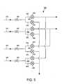
- FIG. 5depicts a first preferred embodiment of a gas switching section of the gas distribution system.
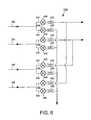
- FIG. 6depicts a second preferred embodiment of the gas switching section of the gas distribution system.
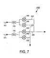
- FIG. 7depicts a third preferred embodiment of the gas switching section of the gas distribution system.
- Plasma processing apparatuses for processing semiconductor materialsinclude a plasma processing chamber and a gas distribution system that supplies process gas into the plasma processing chamber.
- the gas distribution systemcan distribute gas to a single zone or multiple zones across the surface of a substrate during plasma processing.
- the gas distribution systemcan include flow controllers to control the flow ratio of the same or different process gas, or gas mixture, to the zones, thereby allowing in-process adjustment of across-substrate uniformity of gas flow and gas composition.
- multiple-zone gas distribution systemscan provide improved flow control as compared to a single-zone system, it may be desirable to provide such systems with an arrangement that allows substrate processing operations in which the gas composition and/or the gas flow can be changed within a short period of time.
- a gas distribution systemis provided for supplying different gas compositions and/or flow ratios to a chamber.
- the gas distribution systemis adapted to be in fluid communication with an interior of a vacuum chamber, such as a plasma processing chamber of a plasma processing apparatus, and provide the capability of supplying different gas chemistries and/or gas flow rates to the vacuum chamber during processing operations.
- the plasma processing apparatuscan be a low-density, medium-density or high-density plasma reactor including an energy source that uses RF energy, microwave energy, magnetic fields, or the like to produce plasma.
- the high-density plasmacan be produced in a transformer coupled plasma (TCPTM) reactor, also known as an inductively coupled plasma reactor, an electron-cyclotron resonance (ECR) plasma reactor, a capacitive-type discharge, or the like.
- TCPTMtransformer coupled plasma
- ECRelectron-cyclotron resonance
- Exemplary plasma reactors that preferred embodiments of the gas distribution system can be used withinclude ExelanTM plasma reactors, such as the 2300 ExcelanTM plasma reactor, available from Lam Research Corporation, located in Fremont, Calif.
- multiple frequenciescan be applied to a substrate support incorporating an electrode and an electrostatic chuck.
- different frequenciescan be applied to the substrate support and an electrode, such as a showerhead electrode, spaced from the substrate.
- a preferred embodiment of the gas distribution systemcan supply a first gas into the interior of a vacuum chamber, such as a plasma processing chamber, via a single zone or multiple zones, preferably at least an inner zone and an outer zone of a gas distribution member adjacent to an exposed surface of a substrate to be processed.
- the inner and outer zonesare radially spaced, and preferably, flow insulated, from each other in the plasma processing chamber.
- the gas distribution systemcan simultaneously divert a second gas that is different from the first gas to a vacuum chamber by-pass line.
- the by-pass linecan be in fluid communication with a vacuum pump, or the like.
- the first gasis a first process gas and the second gas is a different process gas.
- the first gascan be a first etch gas chemistry or deposition gas chemistry
- the second gascan be a different etch gas chemistry or deposition gas chemistry.
- the gas distribution systemcan simultaneously provide different controlled flow rates of the first gas to the inner zone and the outer zone, respectively, while the second gas is diverted to the by-pass line, and vice versa. By diverting one of the gases to the by-pass line, change over of the gas supplied to the vacuum chamber can be achieved within a short period of time.
- the gas distribution systemincludes switching devices that allow gas switching, or gas change over, in a short period of time between first and second gases supplied to an interior of a vacuum chamber that includes a single zone or includes multiple zones.
- the gas distribution systemcan supply the first gas to the inner zone and outer zone while the second gas is diverted to the by-pass line, and then switch the gas distributions within a short period of time so that the second gas is supplied to the inner zone and outer zone while the first gas is diverted to the by-pass line.
- the gas distribution systemcan alternately supply the first and second gases into the interior of the vacuum chamber, each for a desired period of time to allow quick change over between different processing operations that use different gas chemistries, e.g., alternating steps of a method of processing a semiconductor device.
- the method stepscan be different etch steps, e.g., a faster etch step, such as a main etch, and a relatively slower etch step, such as an over etch step; an etch step and a material deposition step; or different material deposition steps that deposit different materials onto a substrate.
- a volume of a gas composition in a confined region within a vacuum chambercan be replaced (i.e., flushed out) by another gas composition introduced into the vacuum chamber within a short period of time.
- Such gas replacementpreferably can be achieved in less than about 1 s, more preferably within less than about 200 ms, by providing valves having a fast switching capability in the gas distribution system.
- the plasma confinement zonecan have a gas volume of about 1 ⁇ 2 liter to about 4 liters for a plasma processing chamber for processing 200 mm or 300 mm wafers.
- the plasma confinement zonecan be defined by a stack of confinement rings, such as disclosed in commonly-owned U.S. Pat. No. 5,534,751, which is hereby incorporated by reference in its entirety.
- FIG. 1depicts an exemplary semiconductor material plasma processing apparatus 10 that embodiments of the gas distribution system 100 can be used with.
- the apparatus 10comprises a vacuum chamber or plasma processing chamber 12 having an interior containing a substrate support 14 on which a substrate 16 is supported during plasma processing.
- the substrate support 14includes a clamping device, preferably an electrostatic chuck 18 , which is operable to clamp the substrate 16 on the substrate support 14 during processing.
- the substratecan be surrounded by focus rings and/or edge rings, ground extensions or other parts, such as parts disclosed in commonly-owned U.S. Patent Application Publication No. US 2003/0029567, which is incorporated herein by reference in its entirety.
- the plasma processing chamber 12includes a plasma confinement zone having a volume of about 12 liter to about 4 liters, preferably about 1 liter to about 3 liters.
- the plasma processing chamber 12can include a confinement ring arrangement, such as disclosed in commonly-owned U.S. Pat. No. 5,534,751, which is incorporated herein by reference in its entirety, to define the plasma confinement zone.
- the gas distribution systemcan replace such a volume of gas in the plasma confinement zone with another gas within a period of less than about 1 s, preferably in less than about 200 ms, without substantial back diffusion.
- a confinement mechanism, such as confinement rings 120can limit the fluid communication from the plasma volume to portions of the interior of the plasma processing chamber 12 that are outside of the plasma volume.
- the substrate 16may include a base material, such as a silicon wafer; an intermediate layer of a material that is to be processed, e.g., etched, over the base material; and a masking layer over the intermediate layer.
- the intermediate layermay be of a conductive, dielectric, or semiconductive material.
- the masking layercan be patterned photoresist material having an opening pattern for etching desired features, e.g., holes, vias and/or trenches, in the intermediate layer and/or one or more other layers.
- the substratecan include additional layers of conductive, dielectric or semiconductive materials between the base layer and the masking layer, depending on the type of semiconductor device formed on the base material.
- Exemplary dielectric materials that can be processedare, for example, doped silicon oxide, such as fluorinated silicon oxide; un-doped silicon oxide, such as silicon dioxide; spin-on glass; silicate glasses; doped or un-doped thermal silicon oxide; and doped or un-doped TEOS deposited silicon oxide.
- Such dielectric materialscan overlie a conductive or semiconductive layer, such as polycrystalline silicon; metals, such as aluminum, copper, titanium, tungsten, molybdenum and their alloys; nitrides, such as titanium nitride; and metal suicides, such as titanium silicide, tungsten silicide and molybdenum silicide.
- the exemplary plasma processing apparatus 10 shown in FIG. 1includes a showerhead electrode assembly having a support plate 20 forming a wall of the plasma chamber, and a showerhead 22 attached to the support plate.
- a baffle assemblyis located between the showerhead 22 and the support plate 20 to uniformly distribute process gas to a backside 28 of the showerhead.
- the baffle assemblycan include one or more baffle plates.
- the baffle assemblyincludes baffle plates 30 A, 30 B, and 30 C. Open plenums 48 A, 48 B and 48 C are defined between the baffle plates 30 A, 30 B and 30 C; and between the baffle plate 30 C and showerhead 22 .
- the baffle plates 30 A, 30 B and 30 C and showerhead 22include through passages for flowing process gas into the interior of plasma processing chamber 12 .
- a first frequency tuned RF power source 104is controllably connected to a controller 500 and provides power to the showerhead electrode 22 through a first mechanical match box 106 .
- the first frequency tuned RF power source 104provides a variable frequency, which in this embodiment ranges from 1.7 MHz to 2.2 MHz, so that 2 MHz lies within the variable frequency range
- the first frequency tuned RF power sourceis formed to receive and measure output power and reflected RF power and to vary the frequency in the frequency range of 1.7 MHz to 2.2 MHz to minimize reflected RF power from the first frequency tuned RF power source 104 .
- a second frequency tuned RF power source 108is controllably connected to a controller 500 and provides power to the showerhead electrode 22 through a second mechanical match box 110 .
- the second frequency tuned RF power source 108provides a variable frequency, which in this embodiment ranges from 26.7 MHz to 27.2 MHz, so that 27 MHz lies within the variable frequency range.
- the second frequency tuned RF power sourceis formed to receive and measure output power and reflected RF power and to vary the frequency in the frequency range of 26.7 MHz to 27.2 MHz to minimize reflected RF power from the second frequency tuned RF power source 108 .
- a third frequency tuned RF power source 112is controllably connected to a controller 500 and provides power to the showerhead electrode 22 through a third mechanical match box 114 .
- the third frequency tuned RF power source 112provides a variable frequency, which in this embodiment ranges from 59.7 MHz to 60.2 MHz, so that 60 MHz lies within the variable frequency range.
- the third frequency tuned RF power source 112is formed to receive and measure output power and reflected RF power and to vary the frequency in the frequency range of 59.7 MHz to 60.2 MHz to minimize reflected RF power from the third frequency tuned RF power source 112 .
- the first, second, and third frequency tuned RF power sourcesvary the frequency over a range of 0.5 MHz to provide RF tuning.
- the frequency tuned RF power sourcesvary the frequency over a range of less than 2 MHz. More preferably, the frequency tuned RF power sources vary the frequency over a range of less than 1 MHz.
- the tuning rangeshould be large enough to minimize reflected power and yet small enough to allow fast tuning.
- the plenum between the plate 20 and the baffle plate 30 A and the plenums 48 A, 48 B and 48 C between the baffle plates 30 A, 30 B and 30 Care divided into an inner zone 42 and an outer zone 46 by seals 38 a , 38 b , 38 c and 38 d , such as O-rings.
- the inner zone 42 and outer zone 46can be supplied process gas having different respective gas chemistries and/or flow rates by the gas distribution system 100 , preferably under control of the controller 500 .
- Gasis supplied from an inner zone gas supply 40 into the inner zone 42
- gasis supplied from an outer zone gas supply 44 into an annular channel 44 a and then into the outer zone 46 .
- the process gasflows through the passages in the baffle plates 30 A, 30 B and 30 C and the showerhead 22 and into the interior of the plasma processing chamber 12 .
- the plasma processing apparatus 10can include a gas injector system for injecting process gas into the plasma processing chamber.
- the gas injector systemcan have a configuration as disclosed in commonly-owned U.S. patent application Ser. No. 09/788,365, U.S. patent application Ser. No. 10/024,208, U.S. Pat. No. 6,013,155, or U.S. Pat. No. 6,270,862, each of which is incorporated herein by reference in its entirety.
- the process gasis energized into the plasma state in the plasma processing chamber 12 by a power source, such as an RF source driving electrode 22 , or a power source driving an electrode in the substrate support 14 .
- a power sourcesuch as an RF source driving electrode 22 , or a power source driving an electrode in the substrate support 14 .
- the RF power applied to the electrode 22can be varied when different gas compositions are supplied into the plasma processing chamber 12 , preferably within a time period of less than about 1 s, more preferably less than about 200 ms.
- the change in gas compositionscan change the load or impedance from the gas.
- the first, second, and third RF power sources 104 , 108 , 112may have mechanical impedance matching devices, but such devices may not be fast enough to match the changing impedance when different gas compositions are provided for time periods less than about 1 s.
- the first, second, and third RF power sourceshave variable frequencies and are able to measure output and reflected RF power and to vary the frequency to minimize reflected RF power.
- the minimizing the reflected RF powermatches the impedance of the load from the plasma in the processing chamber with the RF power sources through a matchbox.
- FIG. 2shows a preferred embodiment in which the gas distribution system 100 includes a gas supply section 200 , a flow control section 300 , and a gas switching section 400 in fluid communication with each other.
- the gas distribution system 100preferably also includes a controller 500 ( FIG. 1 ), which is connected in control communication to control operation of the gas supply section 200 , flow control section 300 and gas switching section 400 .
- the gas supply section 200can supply different gases, such as first and second process gases, to the flow control section 300 via respective first and second gas lines 235 , 245 .
- the first and second gasescan have different compositions and/or gas flow rates from each other.
- the flow control section 300is operable to control the flow rate, and optionally also to adjust the composition, of different gases that can be supplied to the switching section 400 .
- the flow control section 300can provide different flow rates and/or chemistries of the first and second gases to the switching section 400 via gas passages 324 , 326 and 364 , 366 , respectively.
- the flow rate and/or chemistry of the first gas and/or second gas that is supplied to the plasma processing chamber 12(while the other gas is diverted to by-pass line 50 , which can be in fluid communication with a vacuum pumping system, such as between a turbo pump and a roughing pump) can be different for the inner zone 42 and the outer zone 46 .
- the flow control section 300can provide desired gas flows and/or gas chemistries across the substrate 16 , thereby enhancing substrate processing uniformity.
- the switching section 400is operable to switch from the first gas to the second gas within a short period of time to allow the first gas to be replaced by the second gas in a single zone or multiple zones, e.g., the inner zone 42 and the outer zone 46 , while simultaneously diverting the first gas to the by-pass line, or vice versa.
- the gas switching section 400preferably can switch between the first and second gases without the occurrence of undesirable pressure surges and flow instabilities in the flow of either gas. If desired, the gas distribution system 100 can maintain a substantially constant sequential volumetric flow rate of the first and second gases through the plasma processing chamber 12 .
- FIG. 3shows a preferred embodiment of the gas supply section 200 of the gas distribution system 100 .
- the gas supply section 200is preferably connected to the controller 500 to control operation of flow control components, such as valves and flow controllers, to allow control of the composition of two or more gases that can be supplied by the gas supply section 200 .
- the gas supply section 200includes multiple gas sources 202 , 204 , 206 , 208 , 210 , 212 , 214 and 216 , each being in fluid communication with the first gas line 235 and the second gas line 245 . As such, the gas supply section 200 can supply many different desired gas mixtures to the plasma processing chamber 12 .
- the number of gas sources included in the gas distribution system 100is not limited to any particular number of gas sources, but preferably includes at least two different gas sources.
- the gas supply section 200can include more than or less than the eight gas sources included in the embodiment shown in FIG. 3 .
- the gas supply section 200can include two, three, four, five, ten, twelve, sixteen, or more gas sources.
- the different gases that can be provided by the respective gas sourcesinclude individual gases, such as O 2 , Ar, H 2 , Cl 2 , N 2 and the like, as well as gaseous fluorocarbon and/or fluorohydrocarbon compounds, such as CF 4 , CH 3 F and the like.
- the plasma processing chamberis an etch chamber and the gas sources 202 - 216 can supply Ar, O 2 , N 2 , Cl 2 , CH 3 , CF 4 , C 4 F 8 and CH 3 F or CHF 3 (in any suitable order thereof).
- the particular gases supplied by the respective gas sources 202 - 216can be selected based on the desired process that is to be performed in the plasma processing chamber 12 , e.g., particular dry etching and/or material deposition processes.
- the gas supply section 200can provide broad versatility regarding the choice of gases that can be supplied for performing etching processes and/or material deposition processes.
- the gas supply section 200preferably also includes at least one tuning gas source to adjust the gas composition.
- the tuning gascan be, e.g., O 2 , an inert gas, such as argon, or a reactive gas, such as a fluorocarbon or fluorohydrocarbon gas, e.g., C 4 F 8 .
- the gas supply section 200includes a first tuning gas source 218 and a second tuning gas source 219 . As described below, the first tuning gas source 218 and second tuning gas source 219 can supply tuning gas to adjust the composition of the first and/or second gas supplied to the gas switching section 400 .
- a flow control device 240preferably is disposed in each of the gas passages 222 , 224 , 226 , 228 , 230 , 232 , 234 and 236 in fluid communication with the gas sources 202 , 204 , 206 , 208 , 210 , 212 , 214 and 216 , respectively, and also in the gas passages 242 , 244 in fluid communication with the first tuning gas source 218 and the second tuning gas source 219 , respectively.
- the flow control devices 240are operable to control the flow of the gas supplied by the associated gas sources 202 - 216 and 218 , 219 .
- the flow control devices 240preferably are mass flow controllers (MFCs).
- valves 250 , 252are located along the gas passages downstream of each of the gas sources 202 - 216 .
- the valves 250 , 252can be selectively opened or closed, preferably under control of the controller 500 , to allow different gas mixtures to be flowed to the first gas line 235 and/or the second gas line 245 .
- a first gas mixturecan be supplied to the first gas line 235 .
- a second gas mixturecan be supplied to the second gas line 245 .
- various mixtures and mass flow rates of the first and second gasescan be provided to the first gas line 235 and the second gas line 245 by controlled operation of the gas supply section 200 .
- the gas supply section 200is operable to provide a continuous flow of the first and second gases via the first gas line 235 and the second gas line 245 , respectively.
- the first gas or the second gasis flowed to the plasma processing chamber 12 while the other gas is diverted to the by-pass line.
- the by-pass linecan be connected to a vacuum pump, or the like.
- FIG. 4shows a preferred embodiment of the flow control section 300 of the gas distribution system 100 .
- the flow control section 300includes a first flow control section 305 in fluid communication with the first gas line 235 from the gas supply section 200 , and a second flow control section 315 in fluid communication with the second gas line 245 from the gas supply section 200 .
- the flow control section 300is operable to control the ratio of the first gas supplied to the inner zone 42 and outer zone 46 , respectively, while the second gas is diverted to the by-pass line, and to control the ratio of the second gas supplied to the inner zone 42 and outer zone 46 , respectively, while the first gas is diverted to the by-pass line.
- the first flow control section 305divides the flow of the first gas introduced at the first gas line 235 into two separate outlet flows of the first gas
- the second flow control section 315divides the flow of the second gas introduced at the second gas line 245 into two separate outlet flows of the second gas.
- the first flow control section 305includes first and second gas passages 324 , 326 in fluid communication with the inner zone 42 and outer zone 46 , respectively, via the switching system 400
- the second flow control section 315includes first and second gas passages 364 , 366 in fluid communication with the inner zone 42 and outer zone 46 , respectively, via the switching system 400 .
- the first flow control section 305 and the second flow control section 315each include at least two flow restrictors.
- Each flow restrictorpreferably has a fixed restriction size for gas flow through it.
- the flow restrictorsare preferably orifices.
- the flow restrictorsrestrict gas flow and maintain an approximately constant gas pressure in a region of the gas passages upstream of and proximate the orifices.
- Each of the first flow control section 305 and the second flow control section 315preferably includes a network of orifices, e.g., two, three, four, five or more orifices, each preferably having a different cross-sectional restriction size, e.g., a different diameter or a different cross-sectional area.
- the restriction sizes of the orificesare smaller than the cross-sectional areas of the other portions of the gas flow path of the gas distribution system 100 .
- the orificesare preferably sonic orifices.
- the gas flowsare preferably operated at the critical flow regime in the flow control section 300 so that the flow conductance of a given orifice is determined solely by its restriction size and upstream pressure. As the flow conductance of an orifice increases, the pressure drop across the orifice to achieve a given flow rate through the orifice decreases.
- the first and second flow control sections 305 , 315each include five orifices 330 , 332 , 334 , 336 and 338 .
- the orifices 330 , 332 , 334 , 336 and 338can have relative restriction sizes, e.g., diameters, of one, two, four, eight, and sixteen, respectively. Accordingly, when gas flow occurs through all five orifices 330 - 338 , the four orifices 330 - 336 have approximately the same total conductance as that of the single orifice 338 .
- up to three of the four orifices 330 - 336can be opened to provide different ratios of the total conductance of the orifices 330 - 336 as compared to the conductance of the orifice 338 , in order to supply different ratios of the first gas flow and the second gas flow to the inner zone 42 and the outer zone 46 .
- Another embodimentcan include a different number of orifices, e.g., a total of two orifices; including the orifice 338 and a second orifice that replaces the multiple orifices 330 - 336 .
- the second orificepreferably has the same restriction size as the orifice 338 .
- the flow ratio of the first gas and/or second gas supplied to the inner zone 42 and the outer zone 46is approximately 1:1.
- Valves 320preferably are located upstream of each of the respective orifices 330 - 338 to control the flow of the first and second gases to the orifices.
- one or more of the valves 320can be opened to allow flow of the first gas and/or second gas to one or more of the associated orifice(s) 330 - 336 , while the other valve 320 is opened to allow flow of the first gas and/or the second gas to the orifice(s) 338 .
- the orifices 330 - 336are in fluid communication with the gas passage 322 .
- the gas passage 322is divided into the first and second gas passages 324 , 326 , which are in fluid communication with the gas switching section.
- a pair of valves 320is located in the first and second gas passages 324 , 326 to control flow of the first gas flowed through one or more of the orifices 330 - 336 of the first flow control section 305 to the inner zone 42 and/or the outer zone 46 .
- the pair of valves 320 located along the gas passages 324 , 326can be replaced by a single, four-way valve.
- the orifice 338is arranged along the gas passage 319 .
- the gas passage 319is divided into gas passages 331 , 333 , which are in fluid communication with the first and second gas passages 324 , 326 , respectively.
- a pair of valves 320is located in the gas passages 331 , 333 to control flow of the first gas flowed through the orifice 338 to the first and second gas passages 324 , 326 .
- the pair of valves 320 located along the gas passages 331 , 333can be replaced by a single, four-way valve.
- a pair of valves 320is located along the first and second gas passages 364 , 366 to control flow of the second gas flowed through one or more of the orifices 330 - 336 to the inner zone 42 and the outer zone 46 of the plasma processing chamber.
- the pair of valves 320 located along the gas passages 364 , 366can be replaced by a single, four-way valve.
- the orifice 338is arranged along the gas passage 359 .
- the gas passage 359is divided into gas passages 372 , 374 , which are in fluid communication with the first and second gas passages 364 , 366 , respectively.
- a pair of valves 320is located in the gas passages 372 , 374 to control flow of the second gas flowed through the orifice 338 to the first and/or second gas passages 364 , 366 .
- the pair of valves 320 located along the gas passages 372 , 374can be replaced by a single four-way valve.
- the orifices 330 - 338are included in the flow control section 300 to prevent pressure surges and flow instabilities in the gas flow when the gas distribution system 100 changes the gas flowed into the plasma processing chamber 12 from the first gas to the second gas, and vice versa.
- the gas passage 242 of the first tuning gas source 218( FIG. 3 ) is arranged to supply the first tuning gas to the first gas passage 324 and/or second gas passage 326 of the first flow control section 305 to adjust the first gas composition.
- the gas passage 244 of the second tuning gas source 219( FIG. 3 ) is arranged to supply the second tuning gas to the first gas passage 364 and/or second gas passage 366 of the second flow control section 315 to adjust the second gas composition.
- the first and second tuning gasescan be the same tuning gas or different tuning gases.
- a flow control device 340preferably an MFC, is arranged along the gas passage 242 .
- Valves 320are located along the gas passages 337 , 339 to control flow of the first tuning gas into the gas passage 326 , 324 , respectively.
- the pair of valves 320 located along the gas passages 337 , 339can be replaced by a single, four-way valve.
- a flow control device 340preferably an MFC, is arranged along the gas passage 244 .
- Valves 320are located along the gas passages 376 , 378 to control flow of the second tuning gas into the gas passages 366 , 364 , respectively.
- the pair of valves 320 located along the gas passages 376 , 378can be replaced by a single, four-way valve.
- the first flow control section 305 and the second flow control section 315include the same components arranged in the same configuration.
- the first and second flow control sections 305 , 315can have different components and/or different configurations from each other.
- the first and second flow control sections 305 , 315can include different numbers of orifices and/or orifices with different restriction sizes from each other.
- the gas switching system 400is in fluid communication with the flow control section 300 , and with the interior of the vacuum chamber and the by-pass line to which the first and second gases are flowed.
- a first preferred embodiment of the gas switching system 400is depicted in FIG. 5 .
- the gas switching system 400can alternately supply first and second gases to both the inner zone 42 and the outer zone 46 of the plasma processing chamber 12 .
- the gas switching system 400is in fluid communication with the first gas passage 324 and the second gas passage 326 of the first flow control section 305 , and with the first gas passage 364 and the second gas passage 366 of the second flow control section 315 .
- An orifice 430is arranged along each of the gas passages 324 , 326 , 364 and 366 to prevent undesirable pressure surges during change over of the first and second gases.
- the first gas passage 324 of the first flow control section 305is divided into gas passages 448 , 450 ; the second gas passage 326 of the first flow control section 305 is divided into gas passages 442 , 444 ; the first gas passage 364 of the second flow control section 315 is divided into gas passages 452 , 454 ; and the second gas passage 366 of the second flow control section 315 is divided into gas passages 456 , 458 .
- the gas passage 442is in fluid communication with the outer zone 46 of the plasma chamber 12
- the gas passage 448is in fluid communication with the inner zone 42 of the plasma processing chamber 12
- the gas passage 444provides a by-pass line.
- the gas passage 456is in fluid communication with the gas passage 442 to the outer zone 46 .
- the gas passage 452is in fluid communication with the gas passage 448 to the inner zone 42 .
- the gas passages 450 , 454 and 458are in fluid communication with the gas passage 444 to the by-pass line.
- a valve 440is arranged along each of the gas passages 442 , 444 , 448 , 450 , 452 , 454 , 456 , and 458 .
- each of the pairs of valves 440 located along the gas passages 442 , 444 ; 448 , 450 ; 452 , 454 ; and 456 , 458can be replaced by a single, four-way valve.
- the valves 440can be selectively opened and closed, preferably under control of the controller 500 , to supply the first or second gas to the chamber, while simultaneously diverting the other gas to the by-pass line.
- valves 440 along the gas passages 442 , 448 and 454 , 458are opened, while the valves 440 along the gas passages 444 , 450 and 452 , 456 are closed.
- the valves 440 along the gas passages 444 , 450 and 452 , 456are opened, while the valves 440 along the gas passages 442 , 448 and 454 , 458 are closed.
- a first group of valves 440is opened and a second group of valves 440 is closed to supply the first gas to the plasma processing chamber 12 , and then the same first group of valves is closed and the same second group of valves 440 is opened to change the gas flow to supply the second gas to the plasma processing chamber.
- the valves 440are fast-switching valves.
- the term “fast-switching valve”means a valve that can be opened or closed within a short period of time, preferably less than about 100 ms, more preferably less than about 50 ms, after receiving a signal from the controller 500 to open or close.
- the valves 440are preferably electronically controlled and actuated by receiving a signal from the controller 500 to open or close.
- a suitable “fast-switching valve” that can be used in the gas switching system 400is valve model number FSR-SD-71-6.35, available from Fujikin of America, located in Santa Clara, Calif.
- the gas switching system 400can supply the first gas, e.g., to the interior of the vacuum chamber while diverting the second gas to the by-pass line, and then, preferably under control of the controller 500 , quickly switch these gas flows and supply the second gas to the vacuum chamber while diverting the first gas to the by-pass line.
- the amount of time that the first gas or second gas is supplied to the vacuum chamber before the gases are switchedcan be controlled by the controller 500 .
- the volume of the gas passages 324 , 326 , 364 , and 366 between the associated orifices 430 and the valves 440preferably is less than about 10 cm 3 .
- the gas distribution systemcan be used with a plasma processing chamber including a plasma confinement zone to replace a gas volume of about 1 ⁇ 2 liter to about 4 liters within a period of less than about 1 s, more preferably less than about 200 ms, to thereby stabilize the system.
- a gas switching system 1400 according to a second preferred embodimentis depicted in FIG. 6 .
- a valve 440 and an orifice 430which is located downstream of the valve 440 are arranged along each of the gas passages 442 - 458 .
- the gas switching system 1400can have the same configuration as the gas switching system 400 .
- the orifices 430prevent undesirable pressure surges during switching of gases.
- each of the pairs of valves 440 located along the gas passages 442 , 444 ; 448 , 450 ; 452 , 454 ; and 456 , 458can be replaced by a single, four-way valve.
- a gas switching system 2400according to a third preferred embodiment is depicted in FIG. 7 .
- the gas switching system 2400is in fluid communication with a first gas passage 405 and a second gas passage 415 .
- the first and second gas passages 405 , 415can be, e.g., a first gas outlet and a second gas outlet, respectively, of a flow control section that, unlike the flow control section 300 shown in FIG. 4 , does not include both inner and outer zone gas outlets.
- An orifice 430is located along each of the first gas passage 405 and second gas passage 415 .
- the first gas passage 405is divided into gas passages 422 , 424
- the second gas passage 445is divided into gas passages 426 , 428 .
- the gas passages 422 and 426are in fluid communication with an interior of a vacuum chamber, and the gas passages 424 and 428 are in fluid communication with a by-pass line.
- a valve 440is located along each of the gas passages 422 , 424 and 426 , 428 .
- each of the pairs of valves 440 located along the gas passages 422 , 424 ; and 426 , 428can be replaced by a single, four-way valve.
- valves 440 along the fluid passages 422 and 428are opened and the valves 440 along the gas passages 424 and 426 are closed.
- the valves 440 along the fluid passages 424 and 426are opened and the valves 440 along the fluid passages 422 and 428 are closed.
- the embodiment shown in FIG. 7can be modified by removing the orifices 430 arranged in the first gas passage 405 and second gas passage 415 upstream of the valves 440 , and instead arranging a orifice in each of the gas passages 422 , 424 , 426 and 428 downstream of the associated valves 440 .
- the gas distribution system 100can be used to supply different gas chemistries and/or flow rates to the plasma processing chamber 12 to perform various etching and/or deposition processes.
- the gas distribution system 100can supply process gases to a plasma processing chamber to etch features in a silicon oxide, such as an SiO 2 layer protected by an overlying mask, such as a UV resist mask.
- the SiO 2 layercan be formed on a semiconductor wafer, such as a silicon wafer, having a diameter of 200 mm or 300 mm.
- the featurescan be, e.g., vias and/or trenches.
- a polymeron portions of the mask to repair striations, e.g., cracks or fissures, in the mask (i.e., to fill the striations) so that features etched in the SiO 2 have their desired shape, e.g., vias have a round cross-section. If striations are not repaired, they can eventually reach the layer underlying the mask and in effect be transferred to that layer during etching. Also, a polymer can be deposited on the sidewalls of the features.
- striationse.g., cracks or fissures
- the thickness of the polymer deposited on the sidewalls and the base of etched featuresaffects the etch rate.
- polymer deposited on the bottom of the featureis substantially removed during etching.
- the etch rate of SiO 2is decreased, and may be stopped completely. Polymer may also flake off of surfaces if it becomes too thick.
- the amount of time that the gas mixture for forming the polymer deposit on the mask and features is supplied into the plasma processing chamberis preferably controlled to thereby control the thickness of the polymer deposit formed on the SiO 2 layer, while also providing sufficient repair and protection of the mask.
- the polymeris periodically removed from the mask. Accordingly, the polymer is preferably deposited on the mask between periods of etching of the SiO 2 layer to ensure that sufficient repair and protection of the mask is achieved.
- the gas distribution system 100can be used to supply process gas into a plasma processing chamber to etch SiO 2 protected by an overlying mask, e.g., a UV resist mask, with control of the thickness of polymer deposited on the features, and with repair and protection of the mask.
- the gas switching system of the gas distribution system 100is operable to allow a first process gas used to etch the SiO 2 to be supplied into the plasma processing chamber for a first period of time while a second gas mixture used to form the polymer deposit is diverted to a bypass line, and then to quickly switch the gas flows so that the second gas mixture is supplied into the plasma processing chamber to form the polymer deposit while the first gas mixture is supplied to the by-pass line.
- the first gas mixture supplied to a plasma confinement zone of the plasma processing chamberis at least substantially replaced with the second gas mixture within a period of less than about 1 s, more preferably less than about 200 ms.
- the plasma confinement zonepreferably has a volume of about 1 ⁇ 2 liter to about 4 liters.
- the first gas mixture used to etch SiO 2can contain, e.g., a fluorocarbon species, such as C 4 F 8 , O 2 , and argon.
- the flow ratio of C 4 F 8 /O 2 /argoncan be, e.g., 20/10/500 sccm.
- Poweris provided with at a combination of frequencies of 60 MHz, 27 MHz, and 2 MHz, at powers that can range from 50 to 5000 W.
- the second gas mixture used to form a polymer depositcan contain, e.g., a fluorohydrocarbon species, such as CH 3 F, and argon.
- the flow ratio of CH 3 F/argoncan be, e.g., 15/500 sccm.
- the second gas mixturecan optionally also include O 2 .
- Poweris provided at a combination of frequencies of 60 MHz, 27 MHz, and 2 MHz at powers that can range from 50 to 5000 W.
- the chamber pressurecan be, e.g., 70-90 mTorr.
- the first gas mixtureis preferably flowed into the plasma processing chamber for about 5 seconds to about 20 seconds each time it is introduced into the chamber (while the second gas is diverted to the by-pass line), and the second gas mixture is preferably flowed into the plasma processing chamber for about 1 second to about 3 seconds each time it is introduced into the chamber (while the first gas is diverted to the by-pass line).
- the length of the etching period and/or the polymer deposition periodcan be increased or decreased within the preferred time periods.
- the polymer depositpreferably reaches a maximum thickness of less than about 100 angstroms during the etching process, which typically lasts up to about 3 minutes.
- polymercan be deposited on the mask to repair striations and provide mask protection. Accordingly, the shape of the openings in the mask preferably can be maintained during the etching process.
- the first, second, and third mechanical match boxes 106 , 110 , 114are used to provide gross impedance matching between the first, second, and third frequency tuned RF power sources 104 , 108 , 112 and the load in the plasma processing chamber 12 .
- the first, second, and third mechanical boxes 106 , 110 , 114are not able to precisely match the quickly changing impedance load caused by the quickly changing recipe.
- the inventionuses frequency tuning provided by the first, second, and third frequency tuned RF power sources 104 , 108 , 112 to quickly and precisely match the quickly varying impedance of the load and the first, second, and third mechanical match boxes 106 , 110 , 114 with the impedance of the first, second, and third frequency tuned RF power sources 104 , 108 , 112 .
- the gas volumemust be small to reduce gas transition time in the processing chamber. This is achieved by making the plasma volume as small as possible using confinement rings.
- the RF generatorshave to be able to rapidly tune in to the rapidly varying plasma conditions. This is achieved by using electronically frequency tuned generators rather than conventional mechanical match units. For best critical dimension control (CD) and uniformity control main gases are split and the ratio of center to edge gas flows are selectable. Finally, a tuning gas is needed which can be the same or different from the main gases and can be fed in a selectable flow to the edge or center of the wafer. So, combination of all the aforementioned hardware constitutes the overall performance desired for applied processes put forth in this document.
Landscapes
- Physics & Mathematics (AREA)
- Engineering & Computer Science (AREA)
- Plasma & Fusion (AREA)
- Chemical & Material Sciences (AREA)
- Analytical Chemistry (AREA)
- Drying Of Semiconductors (AREA)
- Plasma Technology (AREA)
- Chemical Vapour Deposition (AREA)
Abstract
Description
- This is a Continuation-In-Part of co-pending prior U.S. application Ser. No. 10/835,175 entitled “GAS DISTRIBUTIONS SYSTEM HAVING FAST GAS SWITCHING CAPABILITIES”, filed on Apr. 30, 2004, which is hereby incorporated by reference.
- Semiconductor structures are processed in plasma processing apparatuses including a plasma processing chamber, a gas source that supplies process gas into the chamber, and an energy source that produces plasma from the process gas. Semiconductor structures are processed in such apparatuses by techniques including dry etching processes, deposition processes, such as chemical vapor deposition (CVD), physical vapor deposition, or plasma-enhanced chemical vapor deposition (PECVD) of metal, dielectric and semiconductor materials and resist stripping processes. Different process gases are used for these processing techniques, as well as processing different materials of semiconductor structures.
- To achieve the foregoing and in accordance with the purpose of the present invention, a plasma wafer processing tool is provided. A plasma chamber with a plasma confinement zone with a volume and at least one electrode is provided. A gas distribution system for providing a first gas and a second gas is connected to the plasma chamber, wherein the gas distribution system can substantially replace one of the first gas and the second gas in the plasma zone with the other of the first gas and the second gas within a period of less than 1 s, wherein a first plasma formed in the plasma zone from the first gas provides a first impedance load and wherein a second plasma formed in the plasma zone from the second gas provides a second impedance load different than the first impedance load. A first frequency tuned RF power source for providing power to the at least one electrode in a first frequency range is electrically connected to the at least one electrode wherein the first frequency tuned RF power source is able to receive reflected RF power and tune an output RF frequency to minimize the reflected RF power. A second frequency tuned RF power source for providing power to the plasma chamber in a second frequency range outside of the first frequency range wherein the second frequency tuned RF power source is able to receive reflected RF power and tune an output RF frequency to minimize the reflected RF power.
- In another manifestation of the invention a plasma processing apparatus is provided. A plasma processing chamber including a showerhead electrode assembly having the inner and outer zones and an interior volume of about ½ liter to 4 liters is provided. A gas distribution system is in fluid communication with the inner and outer zones of the showerhead electrode assembly, wherein the gas distribution system is operable to substantially replace a first process gas or a second process gas in the plasma confinement zone with the other of the first process gas or the second process gas within a period of less than about 1 s. The gas distribution comprises a gas supply system, which provides the first process gas and the second process gas, a flow control system in fluid communication with the gas supply system, which splits a flow of the first process gas into an inner zone flow of the first process gas and an outer zone flow of the first process gas and which splits a flow of the second process gas into an inner zone flow of the second process gas and an outer zone flow of the second process gas, and a switching section, which is in fluid connection between the flow control system and the inner zone and outer zone of the gas distribution member, wherein the switching section switches flow to the inner zone of the gas distribution member between the inner zone flow of the first process gas and the inner zone of the second process gas and wherein the switching section switches flow to the outer zone of the gas distribution member between the outer zone flow of the first process gas and the outer zone flow of the second process gas. A first frequency tuned RF power source for provides power to the plasma processing apparatus in a first frequency range wherein the first frequency tuned RF power source is able to receive reflected RF power and tune an output RF frequency to minimize the reflected RF power. A second frequency tuned RF power source for provides power to the plasma processing apparatus in a second frequency range outside of the first frequency range wherein the second frequency tuned RF power source is able to receive reflected RF power and tune an output RF frequency to minimize the reflected RF power.
- In another manifestation of the invention, a method of processing a semiconductor structure in a plasma processing chamber is provided. a) A first process gas is supplied into the plasma processing chamber while diverting a second process gas to a bypass-line, the plasma processing chamber containing a semiconductor substrate including at least one layer and a patterned resist mask overlying the layer. b) The first process gas is energized to produce a first plasma with a first impedance load and (i) etching at least one feature in the layer or (ii) forming a polymer deposit on the mask. c) A first RF power source is frequency tuned to a first frequency to match the first impedance load. d) A second RF power source is frequency tuned to a second frequency different than the first frequency to match the first impedance load. e) The flows of the first and second process gases are switched so that the second process gas is supplied into the plasma processing chamber while diverting the first process gas to the by-pass line, the first process gas being substantially replaced in a plasma confinement zone of the plasma processing chamber by the second process gas within a period of less than about 1 s. f) The second process gas is energized to produce a second plasma with a second impedance load different from the first impedance load and (iii) etching the at least one feature in the layer or (iv) forming a polymer deposit on the layer and the mask. g) The first RF power source is frequency tuned to a third frequency different than the first and second frequencies to match the second impedance load. h) The second RF power source is frequency tuned to a fourth frequency different than the first, second, and third frequencies to match the second impedance load. i) The flows of the first and second process gases are switched so that the first process gas is supplied into the plasma processing chamber while diverting the second process gas to the by-pass line, the second process gas being substantially replaced in the plasma confinement zone of the plasma processing chamber by the first process gas within a period of less than about 1 s. j) Steps b)-i) are repeated a plurality of times with the substrate.
- These and other features of the present invention will be described in more details below in the detailed description of the invention and in conjunction with the following figures.
- The present invention is illustrated by way of example, and not by way of limitation, in the figures of the accompanying drawings and in which like reference numerals refer to similar elements and in which:
FIG. 1 is a sectional view of an exemplary embodiment of a plasma processing apparatus that preferred embodiments of the gas distribution system can be used with.FIG. 2 illustrates a preferred embodiment of the gas distribution system.FIG. 3 depicts a preferred embodiment of a gas supply section of the gas distribution system.FIG. 4 depicts a preferred embodiment of a flow control section of the gas distribution system.FIG. 5 depicts a first preferred embodiment of a gas switching section of the gas distribution system.FIG. 6 depicts a second preferred embodiment of the gas switching section of the gas distribution system.FIG. 7 depicts a third preferred embodiment of the gas switching section of the gas distribution system.- Plasma processing apparatuses for processing semiconductor materials, such as semiconductor devices formed on semiconductor substrates, e.g., silicon wafers, include a plasma processing chamber and a gas distribution system that supplies process gas into the plasma processing chamber. The gas distribution system can distribute gas to a single zone or multiple zones across the surface of a substrate during plasma processing. The gas distribution system can include flow controllers to control the flow ratio of the same or different process gas, or gas mixture, to the zones, thereby allowing in-process adjustment of across-substrate uniformity of gas flow and gas composition.
- Although multiple-zone gas distribution systems can provide improved flow control as compared to a single-zone system, it may be desirable to provide such systems with an arrangement that allows substrate processing operations in which the gas composition and/or the gas flow can be changed within a short period of time.
- A gas distribution system is provided for supplying different gas compositions and/or flow ratios to a chamber. In a preferred embodiment, the gas distribution system is adapted to be in fluid communication with an interior of a vacuum chamber, such as a plasma processing chamber of a plasma processing apparatus, and provide the capability of supplying different gas chemistries and/or gas flow rates to the vacuum chamber during processing operations. The plasma processing apparatus can be a low-density, medium-density or high-density plasma reactor including an energy source that uses RF energy, microwave energy, magnetic fields, or the like to produce plasma. For example, the high-density plasma can be produced in a transformer coupled plasma (TCP™) reactor, also known as an inductively coupled plasma reactor, an electron-cyclotron resonance (ECR) plasma reactor, a capacitive-type discharge, or the like. Exemplary plasma reactors that preferred embodiments of the gas distribution system can be used with include Exelan™ plasma reactors, such as the 2300 Excelan™ plasma reactor, available from Lam Research Corporation, located in Fremont, Calif. During plasma etching processes, multiple frequencies can be applied to a substrate support incorporating an electrode and an electrostatic chuck. Alternatively, in dual-frequency plasma reactors, different frequencies can be applied to the substrate support and an electrode, such as a showerhead electrode, spaced from the substrate.
- A preferred embodiment of the gas distribution system can supply a first gas into the interior of a vacuum chamber, such as a plasma processing chamber, via a single zone or multiple zones, preferably at least an inner zone and an outer zone of a gas distribution member adjacent to an exposed surface of a substrate to be processed. The inner and outer zones are radially spaced, and preferably, flow insulated, from each other in the plasma processing chamber. The gas distribution system can simultaneously divert a second gas that is different from the first gas to a vacuum chamber by-pass line. The by-pass line can be in fluid communication with a vacuum pump, or the like. In a preferred embodiment, the first gas is a first process gas and the second gas is a different process gas. For example, the first gas can be a first etch gas chemistry or deposition gas chemistry, and the second gas can be a different etch gas chemistry or deposition gas chemistry. The gas distribution system can simultaneously provide different controlled flow rates of the first gas to the inner zone and the outer zone, respectively, while the second gas is diverted to the by-pass line, and vice versa. By diverting one of the gases to the by-pass line, change over of the gas supplied to the vacuum chamber can be achieved within a short period of time.
- The gas distribution system includes switching devices that allow gas switching, or gas change over, in a short period of time between first and second gases supplied to an interior of a vacuum chamber that includes a single zone or includes multiple zones. For multiple-zone systems, the gas distribution system can supply the first gas to the inner zone and outer zone while the second gas is diverted to the by-pass line, and then switch the gas distributions within a short period of time so that the second gas is supplied to the inner zone and outer zone while the first gas is diverted to the by-pass line. The gas distribution system can alternately supply the first and second gases into the interior of the vacuum chamber, each for a desired period of time to allow quick change over between different processing operations that use different gas chemistries, e.g., alternating steps of a method of processing a semiconductor device. In a preferred embodiment, the method steps can be different etch steps, e.g., a faster etch step, such as a main etch, and a relatively slower etch step, such as an over etch step; an etch step and a material deposition step; or different material deposition steps that deposit different materials onto a substrate.
- In a preferred embodiment of the gas distribution system, a volume of a gas composition in a confined region within a vacuum chamber, preferably a plasma confinement zone, can be replaced (i.e., flushed out) by another gas composition introduced into the vacuum chamber within a short period of time. Such gas replacement preferably can be achieved in less than about 1 s, more preferably within less than about 200 ms, by providing valves having a fast switching capability in the gas distribution system. The plasma confinement zone can have a gas volume of about ½ liter to about 4 liters for a plasma processing chamber for processing 200 mm or 300 mm wafers. The plasma confinement zone can be defined by a stack of confinement rings, such as disclosed in commonly-owned U.S. Pat. No. 5,534,751, which is hereby incorporated by reference in its entirety.
FIG. 1 depicts an exemplary semiconductor materialplasma processing apparatus 10 that embodiments of thegas distribution system 100 can be used with. Theapparatus 10 comprises a vacuum chamber orplasma processing chamber 12 having an interior containing asubstrate support 14 on which asubstrate 16 is supported during plasma processing. Thesubstrate support 14 includes a clamping device, preferably anelectrostatic chuck 18, which is operable to clamp thesubstrate 16 on thesubstrate support 14 during processing. The substrate can be surrounded by focus rings and/or edge rings, ground extensions or other parts, such as parts disclosed in commonly-owned U.S. Patent Application Publication No. US 2003/0029567, which is incorporated herein by reference in its entirety.- In a preferred embodiment, the
plasma processing chamber 12 includes a plasma confinement zone having a volume of about 12 liter to about 4 liters, preferably about 1 liter to about 3 liters. For example, theplasma processing chamber 12 can include a confinement ring arrangement, such as disclosed in commonly-owned U.S. Pat. No. 5,534,751, which is incorporated herein by reference in its entirety, to define the plasma confinement zone. The gas distribution system can replace such a volume of gas in the plasma confinement zone with another gas within a period of less than about 1 s, preferably in less than about 200 ms, without substantial back diffusion. A confinement mechanism, such as confinement rings120, can limit the fluid communication from the plasma volume to portions of the interior of theplasma processing chamber 12 that are outside of the plasma volume. - The
substrate 16 may include a base material, such as a silicon wafer; an intermediate layer of a material that is to be processed, e.g., etched, over the base material; and a masking layer over the intermediate layer. The intermediate layer may be of a conductive, dielectric, or semiconductive material. The masking layer can be patterned photoresist material having an opening pattern for etching desired features, e.g., holes, vias and/or trenches, in the intermediate layer and/or one or more other layers. The substrate can include additional layers of conductive, dielectric or semiconductive materials between the base layer and the masking layer, depending on the type of semiconductor device formed on the base material. - Exemplary dielectric materials that can be processed are, for example, doped silicon oxide, such as fluorinated silicon oxide; un-doped silicon oxide, such as silicon dioxide; spin-on glass; silicate glasses; doped or un-doped thermal silicon oxide; and doped or un-doped TEOS deposited silicon oxide. Such dielectric materials can overlie a conductive or semiconductive layer, such as polycrystalline silicon; metals, such as aluminum, copper, titanium, tungsten, molybdenum and their alloys; nitrides, such as titanium nitride; and metal suicides, such as titanium silicide, tungsten silicide and molybdenum silicide.
- The exemplary
plasma processing apparatus 10 shown inFIG. 1 includes a showerhead electrode assembly having asupport plate 20 forming a wall of the plasma chamber, and ashowerhead 22 attached to the support plate. A baffle assembly is located between theshowerhead 22 and thesupport plate 20 to uniformly distribute process gas to abackside 28 of the showerhead. The baffle assembly can include one or more baffle plates. In the embodiment, the baffle assembly includesbaffle plates Open plenums baffle plates baffle plate 30C andshowerhead 22. Thebaffle plates showerhead 22 include through passages for flowing process gas into the interior ofplasma processing chamber 12. - A first frequency tuned
RF power source 104 is controllably connected to acontroller 500 and provides power to theshowerhead electrode 22 through a firstmechanical match box 106. The first frequency tunedRF power source 104 provides a variable frequency, which in this embodiment ranges from 1.7 MHz to 2.2 MHz, so that 2 MHz lies within the variable frequency range The first frequency tuned RF power source is formed to receive and measure output power and reflected RF power and to vary the frequency in the frequency range of 1.7 MHz to 2.2 MHz to minimize reflected RF power from the first frequency tunedRF power source 104. - A second frequency tuned
RF power source 108 is controllably connected to acontroller 500 and provides power to theshowerhead electrode 22 through a secondmechanical match box 110. The second frequency tunedRF power source 108 provides a variable frequency, which in this embodiment ranges from 26.7 MHz to 27.2 MHz, so that 27 MHz lies within the variable frequency range. The second frequency tuned RF power source is formed to receive and measure output power and reflected RF power and to vary the frequency in the frequency range of 26.7 MHz to 27.2 MHz to minimize reflected RF power from the second frequency tunedRF power source 108. - A third frequency tuned
RF power source 112 is controllably connected to acontroller 500 and provides power to theshowerhead electrode 22 through a thirdmechanical match box 114. The third frequency tunedRF power source 112 provides a variable frequency, which in this embodiment ranges from 59.7 MHz to 60.2 MHz, so that 60 MHz lies within the variable frequency range. The third frequency tunedRF power source 112 is formed to receive and measure output power and reflected RF power and to vary the frequency in the frequency range of 59.7 MHz to 60.2 MHz to minimize reflected RF power from the third frequency tunedRF power source 112. - In this example, the first, second, and third frequency tuned RF power sources vary the frequency over a range of 0.5 MHz to provide RF tuning. In other embodiments, the frequency tuned RF power sources vary the frequency over a range of less than 2 MHz. More preferably, the frequency tuned RF power sources vary the frequency over a range of less than 1 MHz. The tuning range should be large enough to minimize reflected power and yet small enough to allow fast tuning.
- In the embodiment, the plenum between the
plate 20 and thebaffle plate 30A and theplenums baffle plates inner zone 42 and anouter zone 46 by seals38a,38b,38cand38d, such as O-rings. Theinner zone 42 andouter zone 46 can be supplied process gas having different respective gas chemistries and/or flow rates by thegas distribution system 100, preferably under control of thecontroller 500. Gas is supplied from an innerzone gas supply 40 into theinner zone 42, and gas is supplied from an outerzone gas supply 44 into an annular channel44aand then into theouter zone 46. The process gas flows through the passages in thebaffle plates showerhead 22 and into the interior of theplasma processing chamber 12. - In other preferred embodiments, the
plasma processing apparatus 10 can include a gas injector system for injecting process gas into the plasma processing chamber. For example, the gas injector system can have a configuration as disclosed in commonly-owned U.S. patent application Ser. No. 09/788,365, U.S. patent application Ser. No. 10/024,208, U.S. Pat. No. 6,013,155, or U.S. Pat. No. 6,270,862, each of which is incorporated herein by reference in its entirety. - The process gas is energized into the plasma state in the
plasma processing chamber 12 by a power source, such as an RFsource driving electrode 22, or a power source driving an electrode in thesubstrate support 14. The RF power applied to theelectrode 22 can be varied when different gas compositions are supplied into theplasma processing chamber 12, preferably within a time period of less than about 1 s, more preferably less than about 200 ms. The change in gas compositions can change the load or impedance from the gas. The first, second, and thirdRF power sources FIG. 2 shows a preferred embodiment in which thegas distribution system 100 includes agas supply section 200, aflow control section 300, and agas switching section 400 in fluid communication with each other. Thegas distribution system 100 preferably also includes a controller500 (FIG. 1 ), which is connected in control communication to control operation of thegas supply section 200,flow control section 300 andgas switching section 400.- In the
gas distribution system 100, thegas supply section 200 can supply different gases, such as first and second process gases, to theflow control section 300 via respective first andsecond gas lines - The
flow control section 300 is operable to control the flow rate, and optionally also to adjust the composition, of different gases that can be supplied to theswitching section 400. Theflow control section 300 can provide different flow rates and/or chemistries of the first and second gases to theswitching section 400 viagas passages pass line 50, which can be in fluid communication with a vacuum pumping system, such as between a turbo pump and a roughing pump) can be different for theinner zone 42 and theouter zone 46. Accordingly, theflow control section 300 can provide desired gas flows and/or gas chemistries across thesubstrate 16, thereby enhancing substrate processing uniformity. - In the
gas distribution system 100, theswitching section 400 is operable to switch from the first gas to the second gas within a short period of time to allow the first gas to be replaced by the second gas in a single zone or multiple zones, e.g., theinner zone 42 and theouter zone 46, while simultaneously diverting the first gas to the by-pass line, or vice versa. Thegas switching section 400 preferably can switch between the first and second gases without the occurrence of undesirable pressure surges and flow instabilities in the flow of either gas. If desired, thegas distribution system 100 can maintain a substantially constant sequential volumetric flow rate of the first and second gases through theplasma processing chamber 12. FIG. 3 shows a preferred embodiment of thegas supply section 200 of thegas distribution system 100. Thegas supply section 200 is preferably connected to thecontroller 500 to control operation of flow control components, such as valves and flow controllers, to allow control of the composition of two or more gases that can be supplied by thegas supply section 200. In the embodiment, thegas supply section 200 includesmultiple gas sources first gas line 235 and thesecond gas line 245. As such, thegas supply section 200 can supply many different desired gas mixtures to theplasma processing chamber 12. The number of gas sources included in thegas distribution system 100 is not limited to any particular number of gas sources, but preferably includes at least two different gas sources. For example, thegas supply section 200 can include more than or less than the eight gas sources included in the embodiment shown inFIG. 3 . For example, thegas supply section 200 can include two, three, four, five, ten, twelve, sixteen, or more gas sources. The different gases that can be provided by the respective gas sources include individual gases, such as O2, Ar, H2, Cl2, N2and the like, as well as gaseous fluorocarbon and/or fluorohydrocarbon compounds, such as CF4, CH3F and the like. In one preferred embodiment, the plasma processing chamber is an etch chamber and the gas sources202-216 can supply Ar, O2, N2, Cl2, CH3, CF4, C4F8and CH3F or CHF3(in any suitable order thereof). The particular gases supplied by the respective gas sources202-216 can be selected based on the desired process that is to be performed in theplasma processing chamber 12, e.g., particular dry etching and/or material deposition processes. Thegas supply section 200 can provide broad versatility regarding the choice of gases that can be supplied for performing etching processes and/or material deposition processes.- The
gas supply section 200 preferably also includes at least one tuning gas source to adjust the gas composition. The tuning gas can be, e.g., O2, an inert gas, such as argon, or a reactive gas, such as a fluorocarbon or fluorohydrocarbon gas, e.g., C4F8. In the embodiment shown inFIG. 3 , thegas supply section 200 includes a firsttuning gas source 218 and a secondtuning gas source 219. As described below, the firsttuning gas source 218 and secondtuning gas source 219 can supply tuning gas to adjust the composition of the first and/or second gas supplied to thegas switching section 400. - In the embodiment of the
gas supply section 200 shown inFIG. 3 , aflow control device 240 preferably is disposed in each of thegas passages gas sources gas passages tuning gas source 218 and the secondtuning gas source 219, respectively. Theflow control devices 240 are operable to control the flow of the gas supplied by the associated gas sources202-216 and218,219. Theflow control devices 240 preferably are mass flow controllers (MFCs). - In the embodiment shown in
FIG. 3 ,valves valves controller 500, to allow different gas mixtures to be flowed to thefirst gas line 235 and/or thesecond gas line 245. For example, by opening thevalves 252 associated with one or more of the gas sources202-216 (while the remainingvalves 252 associated with the other ones of the gas sources202-216 are closed), a first gas mixture can be supplied to thefirst gas line 235. Likewise, by opening thevalves 250 associated with one or more of the other gas sources202-216 (while the remainingvalves 250 associated with the other ones of the gas sources202-216 are closed), a second gas mixture can be supplied to thesecond gas line 245. Accordingly, various mixtures and mass flow rates of the first and second gases can be provided to thefirst gas line 235 and thesecond gas line 245 by controlled operation of thegas supply section 200. - In a preferred embodiment, the
gas supply section 200 is operable to provide a continuous flow of the first and second gases via thefirst gas line 235 and thesecond gas line 245, respectively. The first gas or the second gas is flowed to theplasma processing chamber 12 while the other gas is diverted to the by-pass line. The by-pass line can be connected to a vacuum pump, or the like. By continuously flowing both of the first and second gases, thegas distribution system 100 can achieve rapid change over of the gas flow. FIG. 4 shows a preferred embodiment of theflow control section 300 of thegas distribution system 100. Theflow control section 300 includes a firstflow control section 305 in fluid communication with thefirst gas line 235 from thegas supply section 200, and a secondflow control section 315 in fluid communication with thesecond gas line 245 from thegas supply section 200. Theflow control section 300 is operable to control the ratio of the first gas supplied to theinner zone 42 andouter zone 46, respectively, while the second gas is diverted to the by-pass line, and to control the ratio of the second gas supplied to theinner zone 42 andouter zone 46, respectively, while the first gas is diverted to the by-pass line. The firstflow control section 305 divides the flow of the first gas introduced at thefirst gas line 235 into two separate outlet flows of the first gas, and the secondflow control section 315 divides the flow of the second gas introduced at thesecond gas line 245 into two separate outlet flows of the second gas. The firstflow control section 305 includes first andsecond gas passages inner zone 42 andouter zone 46, respectively, via theswitching system 400, and the secondflow control section 315 includes first andsecond gas passages inner zone 42 andouter zone 46, respectively, via theswitching system 400.- In a preferred arrangement, the first
flow control section 305 and the secondflow control section 315 each include at least two flow restrictors. Each flow restrictor preferably has a fixed restriction size for gas flow through it. The flow restrictors are preferably orifices. The flow restrictors restrict gas flow and maintain an approximately constant gas pressure in a region of the gas passages upstream of and proximate the orifices. Each of the firstflow control section 305 and the secondflow control section 315 preferably includes a network of orifices, e.g., two, three, four, five or more orifices, each preferably having a different cross-sectional restriction size, e.g., a different diameter or a different cross-sectional area. The restriction sizes of the orifices are smaller than the cross-sectional areas of the other portions of the gas flow path of thegas distribution system 100. The orifices are preferably sonic orifices. The gas flows are preferably operated at the critical flow regime in theflow control section 300 so that the flow conductance of a given orifice is determined solely by its restriction size and upstream pressure. As the flow conductance of an orifice increases, the pressure drop across the orifice to achieve a given flow rate through the orifice decreases. - In the embodiment shown in
FIG. 4 , the first and secondflow control sections orifices orifices single orifice 338. Alternatively, up to three of the four orifices330-336 can be opened to provide different ratios of the total conductance of the orifices330-336 as compared to the conductance of theorifice 338, in order to supply different ratios of the first gas flow and the second gas flow to theinner zone 42 and theouter zone 46. - Another embodiment can include a different number of orifices, e.g., a total of two orifices; including the
orifice 338 and a second orifice that replaces the multiple orifices330-336. The second orifice preferably has the same restriction size as theorifice 338. In such embodiment, the flow ratio of the first gas and/or second gas supplied to theinner zone 42 and theouter zone 46 is approximately 1:1. Valves 320 preferably are located upstream of each of the respective orifices330-338 to control the flow of the first and second gases to the orifices. For example, in the firstflow control section 305 and/or the secondflow control section 315, one or more of thevalves 320 can be opened to allow flow of the first gas and/or second gas to one or more of the associated orifice(s)330-336, while theother valve 320 is opened to allow flow of the first gas and/or the second gas to the orifice(s)338.- In the first
flow control section 305, the orifices330-336 are in fluid communication with thegas passage 322. Thegas passage 322 is divided into the first andsecond gas passages valves 320 is located in the first andsecond gas passages flow control section 305 to theinner zone 42 and/or theouter zone 46. In an alternative embodiment, the pair ofvalves 320 located along thegas passages - In the first
flow control section 305, theorifice 338 is arranged along thegas passage 319. Thegas passage 319 is divided intogas passages second gas passages valves 320 is located in thegas passages orifice 338 to the first andsecond gas passages valves 320 located along thegas passages - In the second
flow control section 315, a pair ofvalves 320 is located along the first andsecond gas passages inner zone 42 and theouter zone 46 of the plasma processing chamber. In an alternative embodiment, the pair ofvalves 320 located along thegas passages - In the second
flow control section 315, theorifice 338 is arranged along thegas passage 359. Thegas passage 359 is divided into gas passages372,374, which are in fluid communication with the first andsecond gas passages valves 320 is located in the gas passages372,374 to control flow of the second gas flowed through theorifice 338 to the first and/orsecond gas passages valves 320 located along the gas passages372,374 can be replaced by a single four-way valve. - The orifices330-338 are included in the
flow control section 300 to prevent pressure surges and flow instabilities in the gas flow when thegas distribution system 100 changes the gas flowed into theplasma processing chamber 12 from the first gas to the second gas, and vice versa. - In the embodiment shown in
FIG. 4 , thegas passage 242 of the first tuning gas source218 (FIG. 3 ) is arranged to supply the first tuning gas to thefirst gas passage 324 and/orsecond gas passage 326 of the firstflow control section 305 to adjust the first gas composition. Thegas passage 244 of the second tuning gas source219 (FIG. 3 ) is arranged to supply the second tuning gas to thefirst gas passage 364 and/orsecond gas passage 366 of the secondflow control section 315 to adjust the second gas composition. The first and second tuning gases can be the same tuning gas or different tuning gases. - A
flow control device 340, preferably an MFC, is arranged along thegas passage 242.Valves 320 are located along the gas passages337,339 to control flow of the first tuning gas into thegas passage valves 320 located along the gas passages337,339 can be replaced by a single, four-way valve. - A
flow control device 340, preferably an MFC, is arranged along thegas passage 244.Valves 320 are located along the gas passages376,378 to control flow of the second tuning gas into thegas passages valves 320 located along the gas passages376,378 can be replaced by a single, four-way valve. - In the embodiment of the
flow control section 300 shown inFIG. 4 , the firstflow control section 305 and the secondflow control section 315 include the same components arranged in the same configuration. However, in other preferred embodiments of thegas distribution system 100, the first and secondflow control sections flow control sections - In the
gas distribution system 100, thegas switching system 400 is in fluid communication with theflow control section 300, and with the interior of the vacuum chamber and the by-pass line to which the first and second gases are flowed. A first preferred embodiment of thegas switching system 400 is depicted inFIG. 5 . Thegas switching system 400 can alternately supply first and second gases to both theinner zone 42 and theouter zone 46 of theplasma processing chamber 12. Thegas switching system 400 is in fluid communication with thefirst gas passage 324 and thesecond gas passage 326 of the firstflow control section 305, and with thefirst gas passage 364 and thesecond gas passage 366 of the secondflow control section 315. Anorifice 430 is arranged along each of thegas passages - The
first gas passage 324 of the firstflow control section 305 is divided intogas passages second gas passage 326 of the firstflow control section 305 is divided intogas passages first gas passage 364 of the secondflow control section 315 is divided intogas passages second gas passage 366 of the secondflow control section 315 is divided intogas passages gas passage 442 is in fluid communication with theouter zone 46 of theplasma chamber 12, thegas passage 448 is in fluid communication with theinner zone 42 of theplasma processing chamber 12, and thegas passage 444 provides a by-pass line. Thegas passage 456 is in fluid communication with thegas passage 442 to theouter zone 46. Thegas passage 452 is in fluid communication with thegas passage 448 to theinner zone 42. Thegas passages gas passage 444 to the by-pass line. - A
valve 440 is arranged along each of thegas passages valves 440 located along thegas passages valves 440 can be selectively opened and closed, preferably under control of thecontroller 500, to supply the first or second gas to the chamber, while simultaneously diverting the other gas to the by-pass line. - For example, to supply the first gas to the
inner zone 42 and theouter zone 46 of theplasma processing chamber 12 and divert the second gas to the by-pass line, thevalves 440 along thegas passages valves 440 along thegas passages inner zone 42 and theouter zone 46 of theplasma processing chamber 12, while the first gas is diverted to the by-pass line, thevalves 440 along thegas passages valves 440 along thegas passages valves 440 is opened and a second group ofvalves 440 is closed to supply the first gas to theplasma processing chamber 12, and then the same first group of valves is closed and the same second group ofvalves 440 is opened to change the gas flow to supply the second gas to the plasma processing chamber. - In the
gas switching system 400, thevalves 440 are fast-switching valves. As used herein, the term “fast-switching valve” means a valve that can be opened or closed within a short period of time, preferably less than about 100 ms, more preferably less than about 50 ms, after receiving a signal from thecontroller 500 to open or close. Thevalves 440 are preferably electronically controlled and actuated by receiving a signal from thecontroller 500 to open or close. A suitable “fast-switching valve” that can be used in thegas switching system 400 is valve model number FSR-SD-71-6.35, available from Fujikin of America, located in Santa Clara, Calif. - Accordingly, the
gas switching system 400 can supply the first gas, e.g., to the interior of the vacuum chamber while diverting the second gas to the by-pass line, and then, preferably under control of thecontroller 500, quickly switch these gas flows and supply the second gas to the vacuum chamber while diverting the first gas to the by-pass line. The amount of time that the first gas or second gas is supplied to the vacuum chamber before the gases are switched can be controlled by thecontroller 500. The volume of thegas passages orifices 430 and thevalves 440 preferably is less than about 10 cm3. As explained above, the gas distribution system can be used with a plasma processing chamber including a plasma confinement zone to replace a gas volume of about ½ liter to about 4 liters within a period of less than about 1 s, more preferably less than about 200 ms, to thereby stabilize the system. - A
gas switching system 1400 according to a second preferred embodiment is depicted inFIG. 6 . In thegas switching system 1400, avalve 440 and anorifice 430, which is located downstream of thevalve 440 are arranged along each of the gas passages442-458. Otherwise, thegas switching system 1400 can have the same configuration as thegas switching system 400. Theorifices 430 prevent undesirable pressure surges during switching of gases. In an alternative embodiment, each of the pairs ofvalves 440 located along thegas passages - A
gas switching system 2400 according to a third preferred embodiment is depicted inFIG. 7 . In this embodiment, thegas switching system 2400 is in fluid communication with afirst gas passage 405 and a second gas passage415. The first andsecond gas passages 405,415 can be, e.g., a first gas outlet and a second gas outlet, respectively, of a flow control section that, unlike theflow control section 300 shown inFIG. 4 , does not include both inner and outer zone gas outlets. Anorifice 430 is located along each of thefirst gas passage 405 and second gas passage415. Thefirst gas passage 405 is divided intogas passages gas passages gas passages gas passages valve 440 is located along each of thegas passages valves 440 located along thegas passages - For example, to supply the first gas to the vacuum chamber and simultaneously route the second gas to the by-pass line, the
valves 440 along thefluid passages valves 440 along thegas passages valves 440 along thefluid passages valves 440 along thefluid passages - In another preferred embodiment of the gas switching system, the embodiment shown in
FIG. 7 can be modified by removing theorifices 430 arranged in thefirst gas passage 405 and second gas passage415 upstream of thevalves 440, and instead arranging a orifice in each of thegas passages valves 440. - Preferred embodiments of the
gas distribution system 100 can be used to supply different gas chemistries and/or flow rates to theplasma processing chamber 12 to perform various etching and/or deposition processes. For example, thegas distribution system 100 can supply process gases to a plasma processing chamber to etch features in a silicon oxide, such as an SiO2layer protected by an overlying mask, such as a UV resist mask. The SiO2layer can be formed on a semiconductor wafer, such as a silicon wafer, having a diameter of 200 mm or 300 mm. The features can be, e.g., vias and/or trenches. During such etching processes, it is desirable to deposit a polymer on portions of the mask to repair striations, e.g., cracks or fissures, in the mask (i.e., to fill the striations) so that features etched in the SiO2have their desired shape, e.g., vias have a round cross-section. If striations are not repaired, they can eventually reach the layer underlying the mask and in effect be transferred to that layer during etching. Also, a polymer can be deposited on the sidewalls of the features. - It has been determined, however, that the thickness of the polymer deposited on the sidewalls and the base of etched features affects the etch rate. In anisotropic etching processes, polymer deposited on the bottom of the feature is substantially removed during etching. However, if the polymer becomes too thick on the sidewalls and/or on the base, the etch rate of SiO2is decreased, and may be stopped completely. Polymer may also flake off of surfaces if it becomes too thick. Accordingly, the amount of time that the gas mixture for forming the polymer deposit on the mask and features is supplied into the plasma processing chamber is preferably controlled to thereby control the thickness of the polymer deposit formed on the SiO2layer, while also providing sufficient repair and protection of the mask. During etching of the SiO2layer, polymer is periodically removed from the mask. Accordingly, the polymer is preferably deposited on the mask between periods of etching of the SiO2layer to ensure that sufficient repair and protection of the mask is achieved.
- The
gas distribution system 100 can be used to supply process gas into a plasma processing chamber to etch SiO2protected by an overlying mask, e.g., a UV resist mask, with control of the thickness of polymer deposited on the features, and with repair and protection of the mask. The gas switching system of thegas distribution system 100 is operable to allow a first process gas used to etch the SiO2to be supplied into the plasma processing chamber for a first period of time while a second gas mixture used to form the polymer deposit is diverted to a bypass line, and then to quickly switch the gas flows so that the second gas mixture is supplied into the plasma processing chamber to form the polymer deposit while the first gas mixture is supplied to the by-pass line. Preferably, the first gas mixture supplied to a plasma confinement zone of the plasma processing chamber is at least substantially replaced with the second gas mixture within a period of less than about 1 s, more preferably less than about 200 ms. The plasma confinement zone preferably has a volume of about ½ liter to about 4 liters. - The first gas mixture used to etch SiO2can contain, e.g., a fluorocarbon species, such as C4F8, O2, and argon. The flow ratio of C4F8/O2/argon can be, e.g., 20/10/500 sccm. Power is provided with at a combination of frequencies of 60 MHz, 27 MHz, and 2 MHz, at powers that can range from 50 to 5000 W. The second gas mixture used to form a polymer deposit can contain, e.g., a fluorohydrocarbon species, such as CH3F, and argon. The flow ratio of CH3F/argon can be, e.g., 15/500 sccm. The second gas mixture can optionally also include O2. Power is provided at a combination of frequencies of 60 MHz, 27 MHz, and 2 MHz at powers that can range from 50 to 5000 W. For a capacitive-coupled plasma etch reactor for processing 200 mm or 300 mm wafers, the chamber pressure can be, e.g., 70-90 mTorr. The first gas mixture is preferably flowed into the plasma processing chamber for about 5 seconds to about 20 seconds each time it is introduced into the chamber (while the second gas is diverted to the by-pass line), and the second gas mixture is preferably flowed into the plasma processing chamber for about 1 second to about 3 seconds each time it is introduced into the chamber (while the first gas is diverted to the by-pass line). During etching of SiO2on a substrate, the length of the etching period and/or the polymer deposition period can be increased or decreased within the preferred time periods. The polymer deposit preferably reaches a maximum thickness of less than about 100 angstroms during the etching process, which typically lasts up to about 3 minutes. During etching, polymer can be deposited on the mask to repair striations and provide mask protection. Accordingly, the shape of the openings in the mask preferably can be maintained during the etching process.
- The first, second, and third
mechanical match boxes RF power sources plasma processing chamber 12. The first, second, and thirdmechanical boxes RF power sources mechanical match boxes RF power sources - Since the plasma conditions have to switch very rapidly between deposition and shaping (etch), there are several hardware features which have to work together. The gas volume must be small to reduce gas transition time in the processing chamber. This is achieved by making the plasma volume as small as possible using confinement rings. Also, the RF generators have to be able to rapidly tune in to the rapidly varying plasma conditions. This is achieved by using electronically frequency tuned generators rather than conventional mechanical match units. For best critical dimension control (CD) and uniformity control main gases are split and the ratio of center to edge gas flows are selectable. Finally, a tuning gas is needed which can be the same or different from the main gases and can be fed in a selectable flow to the edge or center of the wafer. So, combination of all the aforementioned hardware constitutes the overall performance desired for applied processes put forth in this document.
- While this invention has been described in terms of several preferred embodiments, there are alterations, permutations, and substitute equivalents, which fall within the scope of this invention. It should also be noted that there are many alternative ways of implementing the methods and apparatuses of the present invention. It is therefore intended that the following appended claims be interpreted as including all such alterations, permutations, and substitute equivalents as fall within the true spirit and scope of the present invention.
Claims (31)
1. A plasma wafer processing tool, comprising:
a plasma chamber with a plasma confinement zone with a volume and at least one electrode;
a gas distribution system for providing a first gas and a second gas, wherein the gas distribution system can substantially replace one of the first gas and the second gas in the plasma zone with the other of the first gas and the second gas within a period of less than 1 s, wherein a first plasma formed in the plasma zone from the first gas provides a first impedance load and wherein a second plasma formed in the plasma zone from the second gas provides a second impedance load different than the first impedance load;
a first frequency tuned RF power source for providing power to the at least one electrode in a first frequency range wherein the first frequency tuned RF power source is able to receive reflected RF power and tune an output RF frequency to minimize the reflected RF power; and
a second frequency tuned RF power source for providing power to the plasma chamber in a second frequency range outside of the first frequency range wherein the second frequency tuned RF power source is able to receive reflected RF power and tune an output RF frequency to minimize the reflected RF power.
2. The plasma wafer processing tool, as recited inclaim 1 , wherein the first frequency tuned RF power source is able to provide a first frequency to impedance match the first impedance load and a second frequency to impedance match the second impedance load, wherein the first frequency is different than the second frequency.
3. The plasma wafer processing tool, as recited inclaim 2 , wherein the second frequency tuned RF power source is able to provide a third frequency to impedance match the first impedance load and a fourth frequency to impedance match the second impedance load, wherein the fourth frequency is different than the first, second, and third frequency.
4. The plasma wafer processing tool, as recited inclaim 3 , wherein the gas distribution system can substantially replace the first gas or the second gas in the plasma zone with the other of the first gas or the second gas within a period of less than 200 ms.
5. The plasma wafer processing tool, as recited inclaim 4 , wherein the plasma chamber further comprises:
a substrate support for supporting a wafer within the plasma chamber; and
a chamber top spaced apart less than 3 cm. from the substrate support.
6. The plasma wafer processing tool, as recited inclaim 5 , further comprising confinement rings spaced apart between the chamber top and substrate support.
7. The plasma wafer processing tool, as recited inclaim 6 , wherein interiors of the confinement rings, the substrate support, and chamber top define the plasma zone.
8. The plasma wafer processing tool, as recited inclaim 7 , wherein the first frequency turned RF power source and the second frequency tuned RF power source tune the output RF frequency over a range of less than 1 MHz.
9. The plasma wafer processing tool, as recited inclaim 1 , wherein the gas distribution system comprises:
a first gas passage and a second gas passage adapted to be in fluid communication with a first gas line;
a third gas passage and a fourth gas passage adapted to be in fluid communication with a second gas line, the first and third gas passages being adapted to supply gas to the vacuum chamber, and the second and fourth gas passages being adapted to supply gas to a by-pass line;
a first fast switching valve arranged along the first gas passage;
a second fast switching valve arranged along the second gas passage;
a third fast switching valve arranged along the third gas passage;
a fourth fast switching valve arranged along the fourth gas passage;
the first and fourth fast switching valves being adapted to receive signals to open while the second and third fast switching valves are closed so that the first gas is supplied to the vacuum chamber via the first gas line and the first and third gas passages while the second gas is supplied to the by-pass line via the second gas line and the second and fourth gas passages; and
the second and third fast switching valves being adapted to receive signals to open while the first and fourth fast switching valves are closed so that the second gas is supplied to the vacuum chamber via the second gas line and the third gas passage while the first gas is supplied to the by-pass line via the first gas line and the second gas passage.
10. The plasma wafer processing tool, as recited inclaim 9 , wherein the gas distribution system further comprises:
a first flow restrictor adapted to be arranged along the first gas line upstream of the first and second fast switching valves; and
a second flow restrictor adapted to be arranged along the second gas line upstream of the third and fourth fast switching valves;
wherein the first and second flow restrictors are adapted to maintain an approximately constant gas pressure in a region of the first and second gas lines upstream of and proximate the first and second flow restrictors.
11. The plasma wafer processing tool, as recited inclaim 10 , wherein the first gas line has a volume between the first flow restrictor and the first and second fast switching valves of less than about 10 cm3, and the second gas line has a volume between the second flow restrictor and the third and fourth fast switching valves of less than about 10 cm3.
12. The plasma wafer processing tool, as recited inclaim 9 , further wherein the gas distribution system further comprises:
a third flow restrictor adapted to be arranged along the first gas passage downstream of the first fast switching valve;
a fourth flow restrictor adapted to be arranged along the second gas passage downstream of the second fast switching valve;
a fifth flow restrictor adapted to be arranged along the third gas passage downstream of the third fast switching valve; and
a sixth flow restrictor adapted to be arranged along the fourth gas passage downstream of the fourth fast switching valve;
wherein the third, fourth, fifth and sixth flow restrictors are adapted to maintain an approximately constant gas pressure in a region of the first, second, third and fourth gas passages upstream of and proximate the respective first, second, third, fourth, fifth and sixth flow restrictors.
13. The plasma wafer processing tool, as recited inclaim 9 , further comprising a controller which is operable to control the opening and closing of the first, second, third and fourth fast switching valves.
14. The plasma wafer processing tool, as recited inclaim 9 , wherein the first, second, third and fourth fast switching valves can be opened and/or closed within a period of less than about 100 ms after receiving a signal.
15. The plasma wafer processing tool, as recited inclaim 1 , further comprising a gas distribution member having an inner zone and outer zone, which are flow insulated from each other.
16. The plasma wafer processing tool, as recited inclaim 15 , wherein the gas distribution system comprises:
a gas supply system, which provides the first gas and the second gas;
a flow control system in fluid communication with the gas supply system, which splits a flow of the first gas into an inner zone flow of the first gas and an outer zone flow of the first gas and which splits a flow of the second gas into an inner zone flow of the second gas and an outer zone flow of the second gas; and
a switching section, which is in fluid connection between the flow control system and the inner zone and outer zone of the gas distribution member, and wherein the switching section switches flow to the inner zone of the gas distribution member between the inner zone flow of the first gas and the inner zone of the second gas and wherein the switching section switches flow to the outer zone of the gas distribution member between the outer zone flow of the first gas and the outer zone flow of the second gas.
17. The plasma wafer processing tool, as recited inclaim 16 , further comprising a by-pass line, wherein the switching section also switches the inner zone flow of the first gas, the inner zone of the second gas, the outer zone flow of the first gas, and the outer zone flow of the second gas to the by-pass line.
18. The plasma wafer processing tool, as recited inclaim 17 , wherein the flow control system further comprising a tuning gas source in fluid connection to at least one of the first gas inner zone flow or first gas outer zone flow after the flow of the first gas is split into the inner zone flow of the first gas and the outer zone flow of the first gas.
19. A plasma processing apparatus, comprising:
a plasma processing chamber including a showerhead electrode assembly having the inner and outer zones and an interior volume of about ½ liter to 4 liters;
the gas distribution system in fluid communication with the inner and outer zones of the showerhead electrode assembly, wherein the gas distribution system being operable to substantially replace a first process gas or a second process gas in the plasma confinement zone with the other of the first process gas or the second process gas within a period of less than about 1 s, comprising:
a gas supply system, which provides the first process gas and the second process gas;
a flow control system in fluid communication with the gas supply system, which splits a flow of the first process gas into an inner zone flow of the first process gas and an outer zone flow of the first process gas and which splits a flow of the second process gas into an inner zone flow of the second process gas and an outer zone flow of the second process gas; and
a switching section, which is in fluid connection between the flow control system and the inner zone and outer zone of the gas distribution member, and wherein the switching section switches flow to the inner zone of the gas distribution member between the inner zone flow of the first process gas and the inner zone of the second process gas and wherein the switching section switches flow to the outer zone of the gas distribution member between the outer zone flow of the first process gas and the outer zone flow of the second process gas;
a first frequency tuned RF power source for providing power to the plasma processing apparatus in a first frequency range wherein the first frequency tuned RF power source is able to receive reflected RF power and tune an output RF frequency to minimize the reflected RF power; and
a second frequency tuned RF power source for providing power to the plasma processing apparatus in a second frequency range outside of the first frequency range wherein the second frequency tuned RF power source is able to receive reflected RF power and tune an output RF frequency to minimize the reflected RF power.
20. The plasma processing apparatus, as recited inclaim 19 , further comprising a by-pass line, wherein the switching section also switches the inner zone flow of the first process gas, the inner zone of the second process gas, the outer zone flow of the first process gas, and the outer zone flow of the second process gas to the by-pass line.
21. The plasma processing apparatus, as recited inclaim 20 , wherein the flow control system further comprising a tuning gas source in fluid connection to at least one of the first process gas inner zone flow or first process gas outer zone flow after the flow of the first process gas is split into the inner zone flow of the first process gas and the outer zone flow of the first process gas.
22. The plasma processing apparatus, as recited inclaim 21 , wherein the first frequency tuned RF power source is able to provide a first frequency to impedance match a first impedance load of a plasma formed from the first process gas and a second frequency to impedance match a second impedance load of a plasma formed from the second plasma gas, wherein the first frequency is different than the second frequency and wherein the second frequency tuned RF power source is able to provide a third frequency to impedance match the first impedance load and a fourth frequency to impedance match the second impedance load, wherein the fourth frequency is different than the first, second, and third frequency.
23. A method of processing a semiconductor structure in a plasma processing chamber, comprising:
a) supplying a first process gas into the plasma processing chamber while diverting a second process gas to a bypass-line, the plasma processing chamber containing a semiconductor substrate including at least one layer and a patterned resist mask overlying the layer;
b) energizing the first process gas to produce a first plasma with a first impedance load and (i) etching at least one feature in the layer or (ii) forming a polymer deposit on the mask;
c) frequency tuning a first RF power source to a first frequency to match the first impedance load;
d) frequency tuning a second RF power source to a second frequency different than the first frequency to match the first impedance load;
e) switching the flows of the first and second process gases so that the second process gas is supplied into the plasma processing chamber while diverting the first process gas to the by-pass line, the first process gas being substantially replaced in a plasma confinement zone of the plasma processing chamber by the second process gas within a period of less than about 1 s;
f) energizing the second process gas to produce a second plasma with a second impedance load different from the first impedance load and (iii) etching the at least one feature in the layer or (iv) forming a polymer deposit on the layer and the mask;
g) frequency tuning the first RF power source to a third frequency different than the first and second frequencies to match the second impedance load;
h) frequency tuning the second RF power source to a fourth frequency different than the first, second, and third frequencies to match the second impedance load;
i) switching the flows of the first and second process gases so that the first process gas is supplied into the plasma processing chamber while diverting the second process gas to the by-pass line, the second process gas being substantially replaced in the plasma confinement zone of the plasma processing chamber by the first process gas within a period of less than about 1 s; and
j) repeating b)-i) a plurality of times with the substrate.
24. The method, as recited inclaim 23 , wherein the periods of less than about 1 s is less than 200 ms.
25. The method, as recited inclaim 23 , wherein the polymer deposit is formed to a maximum thickness of less than about 100 angstroms after repeating a)-i) a plurality of times with the substrate.
26. The method, as recited inclaim 23 , further comprising:
splitting a flow of the first process gas into an inner zone flow and an outer zone flow, wherein the supplying the first process gas into the plasma processing chamber provides the inner zone flow to an inner zone of the processing chamber and the outer zone flow to an outer zone of the processing chamber.
27. The method, as recited inclaim 26 , further comprising providing a tuning gas to at least one of the inner zone flow of the first process gas and the outer zone flow of the first process gas, wherein the tuning gas is provided after the splitting of the flow of the first process gas.
28. The method ofclaim 27 , wherein the first plasma etches the at least one feature in the layer, and the second plasma forms the deposit on the layer and the mask, the deposit repairing striations in the mask.
29. The method ofclaim 23 , wherein the plasma confinement zone has a volume of about ½ liter to about 4 liters.
30. The method, as recited inclaim 23 , wherein:
the first layer is of SiO2;
the mask is a UV-resist mask;
the first process gas comprises a mixture of C4F8, O2and argon and the first plasma etches the layer; and
the second process gas comprises a mixture of CH3F, argon, and optionally O2and the second plasma forms the polymer deposit on the feature and the mask.
31. The method, as recited inclaim 23 , wherein the frequency tuning the first RF power source to a first frequency to match the first impedance load, and the frequency tuning the first RF power source to a third frequency to match the second impedance load use a matchbox to partially match the first impedance load and third impedance load and use frequency tuning to provide a final match of the first impedance load and second impedance load.
Priority Applications (7)
| Application Number | Priority Date | Filing Date | Title |
|---|---|---|---|
| US11/601,293US20070066038A1 (en) | 2004-04-30 | 2006-11-17 | Fast gas switching plasma processing apparatus |
| CN2007800426835ACN101563757B (en) | 2006-11-17 | 2007-11-12 | Fast gas switching plasma processing apparatus |
| PCT/US2007/084465WO2008061069A1 (en) | 2006-11-17 | 2007-11-12 | Fast gas switching plasma processing apparatus |
| JP2009537300AJP5014435B2 (en) | 2006-11-17 | 2007-11-12 | High-speed gas switching plasma processing equipment |
| KR1020097012509AKR101432850B1 (en) | 2006-11-17 | 2007-11-12 | High-speed gas switching plasma processing device |
| TW096143232ATWI417945B (en) | 2006-11-17 | 2007-11-15 | Fast gas switching plasma processing apparatus |
| US13/189,416US8343876B2 (en) | 2004-04-30 | 2011-07-22 | Fast gas switching plasma processing apparatus |
Applications Claiming Priority (2)
| Application Number | Priority Date | Filing Date | Title |
|---|---|---|---|
| US10/835,175US7708859B2 (en) | 2004-04-30 | 2004-04-30 | Gas distribution system having fast gas switching capabilities |
| US11/601,293US20070066038A1 (en) | 2004-04-30 | 2006-11-17 | Fast gas switching plasma processing apparatus |
Related Parent Applications (1)
| Application Number | Title | Priority Date | Filing Date |
|---|---|---|---|
| US10/835,175Continuation-In-PartUS7708859B2 (en) | 2004-04-30 | 2004-04-30 | Gas distribution system having fast gas switching capabilities |
Related Child Applications (1)
| Application Number | Title | Priority Date | Filing Date |
|---|---|---|---|
| US13/189,416DivisionUS8343876B2 (en) | 2004-04-30 | 2011-07-22 | Fast gas switching plasma processing apparatus |
Publications (1)
| Publication Number | Publication Date |
|---|---|
| US20070066038A1true US20070066038A1 (en) | 2007-03-22 |
Family
ID=39402006
Family Applications (2)
| Application Number | Title | Priority Date | Filing Date |
|---|---|---|---|
| US11/601,293AbandonedUS20070066038A1 (en) | 2004-04-30 | 2006-11-17 | Fast gas switching plasma processing apparatus |
| US13/189,416Expired - Fee RelatedUS8343876B2 (en) | 2004-04-30 | 2011-07-22 | Fast gas switching plasma processing apparatus |
Family Applications After (1)
| Application Number | Title | Priority Date | Filing Date |
|---|---|---|---|
| US13/189,416Expired - Fee RelatedUS8343876B2 (en) | 2004-04-30 | 2011-07-22 | Fast gas switching plasma processing apparatus |
Country Status (6)
| Country | Link |
|---|---|
| US (2) | US20070066038A1 (en) |
| JP (1) | JP5014435B2 (en) |
| KR (1) | KR101432850B1 (en) |
| CN (1) | CN101563757B (en) |
| TW (1) | TWI417945B (en) |
| WO (1) | WO2008061069A1 (en) |
Cited By (358)
| Publication number | Priority date | Publication date | Assignee | Title |
|---|---|---|---|---|
| US20070259130A1 (en)* | 2004-06-08 | 2007-11-08 | Hans Von Kaenel | System for Low-Energy Plasma-Enhanced Chemical Vapor Deposition |
| US20080242085A1 (en)* | 2007-03-30 | 2008-10-02 | Lam Research Corporation | Showerhead electrodes and showerhead electrode assemblies having low-particle performance for semiconductor material processing apparatuses |
| US20090061640A1 (en)* | 2007-08-29 | 2009-03-05 | Lam Research Corporation | Alternate gas delivery and evacuation system for plasma processing apparatuses |
| US20090064932A1 (en)* | 2007-08-31 | 2009-03-12 | Samsung Electronics Co., Ltd. | Apparatus for HDP-CVD and method of forming insulating layer using the same |
| US20090236040A1 (en)* | 2008-03-18 | 2009-09-24 | Lam Research Corporation | Electrode assembly and plasma processing chamber utilizing thermally conductive gasket |
| US20090260763A1 (en)* | 2008-04-22 | 2009-10-22 | Micron Technology, Inc. | Plasma processing with preionized and predissociated tuning gases and associated systems and methods |
| US20090286397A1 (en)* | 2008-05-15 | 2009-11-19 | Lam Research Corporation | Selective inductive double patterning |
| CN102201331A (en)* | 2010-03-26 | 2011-09-28 | 东京毅力科创株式会社 | Substrate processing method |
| US8133349B1 (en) | 2010-11-03 | 2012-03-13 | Lam Research Corporation | Rapid and uniform gas switching for a plasma etch process |
| US8343876B2 (en) | 2004-04-30 | 2013-01-01 | Lam Research Corporation | Fast gas switching plasma processing apparatus |
| WO2013006759A1 (en)* | 2011-07-06 | 2013-01-10 | Lam Research Corporation | Synchronized and shortened master-slave rf pulsing in a plasma processing chamber |
| JP2013171840A (en)* | 2012-02-22 | 2013-09-02 | Lam Research Corporation | Frequency enhanced impedance dependent power control for multi-frequency rf pulsing |
| US8562785B2 (en) | 2011-05-31 | 2013-10-22 | Lam Research Corporation | Gas distribution showerhead for inductively coupled plasma etch reactor |
| US20140262025A1 (en)* | 2009-08-20 | 2014-09-18 | Tokyo Electron Limited | Plasma processing apparatus and plasma etching apparatus |
| US20150053346A1 (en)* | 2010-06-28 | 2015-02-26 | Tokyo Electron Limited | Plasma processing apparatus and plasma processing method |
| US9023177B2 (en) | 2008-10-15 | 2015-05-05 | Lam Research Corporation | Anchoring inserts, electrode assemblies, and plasma processing chambers |
| US9245717B2 (en) | 2011-05-31 | 2016-01-26 | Lam Research Corporation | Gas distribution system for ceramic showerhead of plasma etch reactor |
| US20160027618A1 (en)* | 2014-07-24 | 2016-01-28 | Hitachi High-Technologies Corporation | Plasma processing apparatus and plasma processing method |
| US20160163554A1 (en)* | 2014-12-04 | 2016-06-09 | Tokyo Electron Limited | Plasma etching method |
| US20170032982A1 (en)* | 2015-07-30 | 2017-02-02 | Lam Research Corporation | Gas delivery system |
| US9679751B2 (en) | 2012-03-15 | 2017-06-13 | Lam Research Corporation | Chamber filler kit for plasma etch chamber useful for fast gas switching |
| US10147588B2 (en) | 2016-02-12 | 2018-12-04 | Lam Research Corporation | System and method for increasing electron density levels in a plasma of a substrate processing system |
| US10192751B2 (en) | 2015-10-15 | 2019-01-29 | Lam Research Corporation | Systems and methods for ultrahigh selective nitride etch |
| US10364493B2 (en) | 2016-08-25 | 2019-07-30 | Asm Ip Holding B.V. | Exhaust apparatus and substrate processing apparatus having an exhaust line with a first ring having at least one hole on a lateral side thereof placed in the exhaust line |
| US10410832B2 (en) | 2016-08-19 | 2019-09-10 | Lam Research Corporation | Control of on-wafer CD uniformity with movable edge ring and gas injection adjustment |
| US10438833B2 (en) | 2016-02-16 | 2019-10-08 | Lam Research Corporation | Wafer lift ring system for wafer transfer |
| US20190323125A1 (en)* | 2018-04-18 | 2019-10-24 | Lam Research Corporation | Substrate processing systems including gas delivery system with reduced dead legs |
| US10541145B2 (en)* | 2017-03-29 | 2020-01-21 | Tokyo Electron Limited | Substrate processing apparatus and substrate processing method |
| US10559458B1 (en) | 2018-11-26 | 2020-02-11 | Asm Ip Holding B.V. | Method of forming oxynitride film |
| US10561975B2 (en) | 2014-10-07 | 2020-02-18 | Asm Ip Holdings B.V. | Variable conductance gas distribution apparatus and method |
| USD876504S1 (en) | 2017-04-03 | 2020-02-25 | Asm Ip Holding B.V. | Exhaust flow control ring for semiconductor deposition apparatus |
| US10590535B2 (en) | 2017-07-26 | 2020-03-17 | Asm Ip Holdings B.V. | Chemical treatment, deposition and/or infiltration apparatus and method for using the same |
| US10600673B2 (en) | 2015-07-07 | 2020-03-24 | Asm Ip Holding B.V. | Magnetic susceptor to baseplate seal |
| US10604847B2 (en) | 2014-03-18 | 2020-03-31 | Asm Ip Holding B.V. | Gas distribution system, reactor including the system, and methods of using the same |
| US10612136B2 (en) | 2018-06-29 | 2020-04-07 | ASM IP Holding, B.V. | Temperature-controlled flange and reactor system including same |
| US10622375B2 (en) | 2016-11-07 | 2020-04-14 | Asm Ip Holding B.V. | Method of processing a substrate and a device manufactured by using the method |
| US10643826B2 (en) | 2016-10-26 | 2020-05-05 | Asm Ip Holdings B.V. | Methods for thermally calibrating reaction chambers |
| US10643904B2 (en) | 2016-11-01 | 2020-05-05 | Asm Ip Holdings B.V. | Methods for forming a semiconductor device and related semiconductor device structures |
| US10651015B2 (en) | 2016-02-12 | 2020-05-12 | Lam Research Corporation | Variable depth edge ring for etch uniformity control |
| US10658205B2 (en) | 2017-09-28 | 2020-05-19 | Asm Ip Holdings B.V. | Chemical dispensing apparatus and methods for dispensing a chemical to a reaction chamber |
| US10658181B2 (en) | 2018-02-20 | 2020-05-19 | Asm Ip Holding B.V. | Method of spacer-defined direct patterning in semiconductor fabrication |
| US10655221B2 (en) | 2017-02-09 | 2020-05-19 | Asm Ip Holding B.V. | Method for depositing oxide film by thermal ALD and PEALD |
| US10665452B2 (en) | 2016-05-02 | 2020-05-26 | Asm Ip Holdings B.V. | Source/drain performance through conformal solid state doping |
| US10672636B2 (en) | 2017-08-09 | 2020-06-02 | Asm Ip Holding B.V. | Cassette holder assembly for a substrate cassette and holding member for use in such assembly |
| US10685834B2 (en) | 2017-07-05 | 2020-06-16 | Asm Ip Holdings B.V. | Methods for forming a silicon germanium tin layer and related semiconductor device structures |
| US10683571B2 (en) | 2014-02-25 | 2020-06-16 | Asm Ip Holding B.V. | Gas supply manifold and method of supplying gases to chamber using same |
| US10692741B2 (en) | 2017-08-08 | 2020-06-23 | Asm Ip Holdings B.V. | Radiation shield |
| US10699909B2 (en) | 2014-11-11 | 2020-06-30 | Hitach High-Tech Corporation | Plasma processing apparatus and plasma processing method |
| US10699878B2 (en) | 2016-02-12 | 2020-06-30 | Lam Research Corporation | Chamber member of a plasma source and pedestal with radially outward positioned lift pins for translation of a substrate c-ring |
| US10707106B2 (en) | 2011-06-06 | 2020-07-07 | Asm Ip Holding B.V. | High-throughput semiconductor-processing apparatus equipped with multiple dual-chamber modules |
| US10714335B2 (en) | 2017-04-25 | 2020-07-14 | Asm Ip Holding B.V. | Method of depositing thin film and method of manufacturing semiconductor device |
| US10714385B2 (en) | 2016-07-19 | 2020-07-14 | Asm Ip Holding B.V. | Selective deposition of tungsten |
| US10714315B2 (en) | 2012-10-12 | 2020-07-14 | Asm Ip Holdings B.V. | Semiconductor reaction chamber showerhead |
| US10714350B2 (en) | 2016-11-01 | 2020-07-14 | ASM IP Holdings, B.V. | Methods for forming a transition metal niobium nitride film on a substrate by atomic layer deposition and related semiconductor device structures |
| US10720322B2 (en) | 2016-02-19 | 2020-07-21 | Asm Ip Holding B.V. | Method for forming silicon nitride film selectively on top surface |
| US10720331B2 (en) | 2016-11-01 | 2020-07-21 | ASM IP Holdings, B.V. | Methods for forming a transition metal nitride film on a substrate by atomic layer deposition and related semiconductor device structures |
| US10734244B2 (en) | 2017-11-16 | 2020-08-04 | Asm Ip Holding B.V. | Method of processing a substrate and a device manufactured by the same |
| US10731249B2 (en) | 2018-02-15 | 2020-08-04 | Asm Ip Holding B.V. | Method of forming a transition metal containing film on a substrate by a cyclical deposition process, a method for supplying a transition metal halide compound to a reaction chamber, and related vapor deposition apparatus |
| US10734223B2 (en) | 2017-10-10 | 2020-08-04 | Asm Ip Holding B.V. | Method for depositing a metal chalcogenide on a substrate by cyclical deposition |
| US10734497B2 (en) | 2017-07-18 | 2020-08-04 | Asm Ip Holding B.V. | Methods for forming a semiconductor device structure and related semiconductor device structures |
| US10741385B2 (en) | 2016-07-28 | 2020-08-11 | Asm Ip Holding B.V. | Method and apparatus for filling a gap |
| US10755923B2 (en) | 2018-07-03 | 2020-08-25 | Asm Ip Holding B.V. | Method for depositing silicon-free carbon-containing film as gap-fill layer by pulse plasma-assisted deposition |
| US10755922B2 (en) | 2018-07-03 | 2020-08-25 | Asm Ip Holding B.V. | Method for depositing silicon-free carbon-containing film as gap-fill layer by pulse plasma-assisted deposition |
| US10770336B2 (en) | 2017-08-08 | 2020-09-08 | Asm Ip Holding B.V. | Substrate lift mechanism and reactor including same |
| US10770286B2 (en) | 2017-05-08 | 2020-09-08 | Asm Ip Holdings B.V. | Methods for selectively forming a silicon nitride film on a substrate and related semiconductor device structures |
| US10767789B2 (en) | 2018-07-16 | 2020-09-08 | Asm Ip Holding B.V. | Diaphragm valves, valve components, and methods for forming valve components |
| US10784102B2 (en) | 2016-12-22 | 2020-09-22 | Asm Ip Holding B.V. | Method of forming a structure on a substrate |
| US10787741B2 (en) | 2014-08-21 | 2020-09-29 | Asm Ip Holding B.V. | Method and system for in situ formation of gas-phase compounds |
| US10797133B2 (en) | 2018-06-21 | 2020-10-06 | Asm Ip Holding B.V. | Method for depositing a phosphorus doped silicon arsenide film and related semiconductor device structures |
| US10804098B2 (en) | 2009-08-14 | 2020-10-13 | Asm Ip Holding B.V. | Systems and methods for thin-film deposition of metal oxides using excited nitrogen-oxygen species |
| US10811256B2 (en) | 2018-10-16 | 2020-10-20 | Asm Ip Holding B.V. | Method for etching a carbon-containing feature |
| USD900036S1 (en) | 2017-08-24 | 2020-10-27 | Asm Ip Holding B.V. | Heater electrical connector and adapter |
| US10818758B2 (en) | 2018-11-16 | 2020-10-27 | Asm Ip Holding B.V. | Methods for forming a metal silicate film on a substrate in a reaction chamber and related semiconductor device structures |
| US10825659B2 (en) | 2016-01-07 | 2020-11-03 | Lam Research Corporation | Substrate processing chamber including multiple gas injection points and dual injector |
| US10832903B2 (en) | 2011-10-28 | 2020-11-10 | Asm Ip Holding B.V. | Process feed management for semiconductor substrate processing |
| US10829852B2 (en) | 2018-08-16 | 2020-11-10 | Asm Ip Holding B.V. | Gas distribution device for a wafer processing apparatus |
| US10847365B2 (en) | 2018-10-11 | 2020-11-24 | Asm Ip Holding B.V. | Method of forming conformal silicon carbide film by cyclic CVD |
| US10844484B2 (en) | 2017-09-22 | 2020-11-24 | Asm Ip Holding B.V. | Apparatus for dispensing a vapor phase reactant to a reaction chamber and related methods |
| US10847366B2 (en) | 2018-11-16 | 2020-11-24 | Asm Ip Holding B.V. | Methods for depositing a transition metal chalcogenide film on a substrate by a cyclical deposition process |
| US10844486B2 (en) | 2009-04-06 | 2020-11-24 | Asm Ip Holding B.V. | Semiconductor processing reactor and components thereof |
| US10847371B2 (en) | 2018-03-27 | 2020-11-24 | Asm Ip Holding B.V. | Method of forming an electrode on a substrate and a semiconductor device structure including an electrode |
| USD903477S1 (en) | 2018-01-24 | 2020-12-01 | Asm Ip Holdings B.V. | Metal clamp |
| US10851456B2 (en) | 2016-04-21 | 2020-12-01 | Asm Ip Holding B.V. | Deposition of metal borides |
| US10854498B2 (en) | 2011-07-15 | 2020-12-01 | Asm Ip Holding B.V. | Wafer-supporting device and method for producing same |
| US10858737B2 (en) | 2014-07-28 | 2020-12-08 | Asm Ip Holding B.V. | Showerhead assembly and components thereof |
| US10867786B2 (en) | 2018-03-30 | 2020-12-15 | Asm Ip Holding B.V. | Substrate processing method |
| US10867788B2 (en) | 2016-12-28 | 2020-12-15 | Asm Ip Holding B.V. | Method of forming a structure on a substrate |
| US10865475B2 (en) | 2016-04-21 | 2020-12-15 | Asm Ip Holding B.V. | Deposition of metal borides and silicides |
| US10872771B2 (en) | 2018-01-16 | 2020-12-22 | Asm Ip Holding B. V. | Method for depositing a material film on a substrate within a reaction chamber by a cyclical deposition process and related device structures |
| US10883175B2 (en) | 2018-08-09 | 2021-01-05 | Asm Ip Holding B.V. | Vertical furnace for processing substrates and a liner for use therein |
| US10892156B2 (en) | 2017-05-08 | 2021-01-12 | Asm Ip Holding B.V. | Methods for forming a silicon nitride film on a substrate and related semiconductor device structures |
| US10896820B2 (en) | 2018-02-14 | 2021-01-19 | Asm Ip Holding B.V. | Method for depositing a ruthenium-containing film on a substrate by a cyclical deposition process |
| US10910262B2 (en) | 2017-11-16 | 2021-02-02 | Asm Ip Holding B.V. | Method of selectively depositing a capping layer structure on a semiconductor device structure |
| US10914004B2 (en) | 2018-06-29 | 2021-02-09 | Asm Ip Holding B.V. | Thin-film deposition method and manufacturing method of semiconductor device |
| US10923344B2 (en) | 2017-10-30 | 2021-02-16 | Asm Ip Holding B.V. | Methods for forming a semiconductor structure and related semiconductor structures |
| US10928731B2 (en) | 2017-09-21 | 2021-02-23 | Asm Ip Holding B.V. | Method of sequential infiltration synthesis treatment of infiltrateable material and structures and devices formed using same |
| US10934619B2 (en) | 2016-11-15 | 2021-03-02 | Asm Ip Holding B.V. | Gas supply unit and substrate processing apparatus including the gas supply unit |
| US10941490B2 (en) | 2014-10-07 | 2021-03-09 | Asm Ip Holding B.V. | Multiple temperature range susceptor, assembly, reactor and system including the susceptor, and methods of using the same |
| USD913980S1 (en) | 2018-02-01 | 2021-03-23 | Asm Ip Holding B.V. | Gas supply plate for semiconductor manufacturing apparatus |
| US10975470B2 (en) | 2018-02-23 | 2021-04-13 | Asm Ip Holding B.V. | Apparatus for detecting or monitoring for a chemical precursor in a high temperature environment |
| US11004977B2 (en) | 2017-07-19 | 2021-05-11 | Asm Ip Holding B.V. | Method for depositing a group IV semiconductor and related semiconductor device structures |
| US11001925B2 (en) | 2016-12-19 | 2021-05-11 | Asm Ip Holding B.V. | Substrate processing apparatus |
| US11018047B2 (en) | 2018-01-25 | 2021-05-25 | Asm Ip Holding B.V. | Hybrid lift pin |
| US11015245B2 (en) | 2014-03-19 | 2021-05-25 | Asm Ip Holding B.V. | Gas-phase reactor and system having exhaust plenum and components thereof |
| US11018002B2 (en) | 2017-07-19 | 2021-05-25 | Asm Ip Holding B.V. | Method for selectively depositing a Group IV semiconductor and related semiconductor device structures |
| US11022879B2 (en) | 2017-11-24 | 2021-06-01 | Asm Ip Holding B.V. | Method of forming an enhanced unexposed photoresist layer |
| US11024523B2 (en) | 2018-09-11 | 2021-06-01 | Asm Ip Holding B.V. | Substrate processing apparatus and method |
| US11031242B2 (en) | 2018-11-07 | 2021-06-08 | Asm Ip Holding B.V. | Methods for depositing a boron doped silicon germanium film |
| USD922229S1 (en) | 2019-06-05 | 2021-06-15 | Asm Ip Holding B.V. | Device for controlling a temperature of a gas supply unit |
| US11049751B2 (en) | 2018-09-14 | 2021-06-29 | Asm Ip Holding B.V. | Cassette supply system to store and handle cassettes and processing apparatus equipped therewith |
| US11053591B2 (en) | 2018-08-06 | 2021-07-06 | Asm Ip Holding B.V. | Multi-port gas injection system and reactor system including same |
| US11056567B2 (en) | 2018-05-11 | 2021-07-06 | Asm Ip Holding B.V. | Method of forming a doped metal carbide film on a substrate and related semiconductor device structures |
| US11056344B2 (en) | 2017-08-30 | 2021-07-06 | Asm Ip Holding B.V. | Layer forming method |
| US11069510B2 (en) | 2017-08-30 | 2021-07-20 | Asm Ip Holding B.V. | Substrate processing apparatus |
| US11081345B2 (en) | 2018-02-06 | 2021-08-03 | Asm Ip Holding B.V. | Method of post-deposition treatment for silicon oxide film |
| US11088002B2 (en) | 2018-03-29 | 2021-08-10 | Asm Ip Holding B.V. | Substrate rack and a substrate processing system and method |
| US11087997B2 (en) | 2018-10-31 | 2021-08-10 | Asm Ip Holding B.V. | Substrate processing apparatus for processing substrates |
| US11094582B2 (en) | 2016-07-08 | 2021-08-17 | Asm Ip Holding B.V. | Selective deposition method to form air gaps |
| US11094546B2 (en) | 2017-10-05 | 2021-08-17 | Asm Ip Holding B.V. | Method for selectively depositing a metallic film on a substrate |
| US11101370B2 (en) | 2016-05-02 | 2021-08-24 | Asm Ip Holding B.V. | Method of forming a germanium oxynitride film |
| US11114283B2 (en) | 2018-03-16 | 2021-09-07 | Asm Ip Holding B.V. | Reactor, system including the reactor, and methods of manufacturing and using same |
| US11114294B2 (en) | 2019-03-08 | 2021-09-07 | Asm Ip Holding B.V. | Structure including SiOC layer and method of forming same |
| USD930782S1 (en) | 2019-08-22 | 2021-09-14 | Asm Ip Holding B.V. | Gas distributor |
| US11127617B2 (en) | 2017-11-27 | 2021-09-21 | Asm Ip Holding B.V. | Storage device for storing wafer cassettes for use with a batch furnace |
| US11127589B2 (en) | 2019-02-01 | 2021-09-21 | Asm Ip Holding B.V. | Method of topology-selective film formation of silicon oxide |
| USD931978S1 (en) | 2019-06-27 | 2021-09-28 | Asm Ip Holding B.V. | Showerhead vacuum transport |
| US11139308B2 (en) | 2015-12-29 | 2021-10-05 | Asm Ip Holding B.V. | Atomic layer deposition of III-V compounds to form V-NAND devices |
| US11139191B2 (en) | 2017-08-09 | 2021-10-05 | Asm Ip Holding B.V. | Storage apparatus for storing cassettes for substrates and processing apparatus equipped therewith |
| US11158513B2 (en) | 2018-12-13 | 2021-10-26 | Asm Ip Holding B.V. | Methods for forming a rhenium-containing film on a substrate by a cyclical deposition process and related semiconductor device structures |
| USD935572S1 (en) | 2019-05-24 | 2021-11-09 | Asm Ip Holding B.V. | Gas channel plate |
| US11171025B2 (en) | 2019-01-22 | 2021-11-09 | Asm Ip Holding B.V. | Substrate processing device |
| US11205585B2 (en) | 2016-07-28 | 2021-12-21 | Asm Ip Holding B.V. | Substrate processing apparatus and method of operating the same |
| US11217444B2 (en) | 2018-11-30 | 2022-01-04 | Asm Ip Holding B.V. | Method for forming an ultraviolet radiation responsive metal oxide-containing film |
| US11222772B2 (en) | 2016-12-14 | 2022-01-11 | Asm Ip Holding B.V. | Substrate processing apparatus |
| CN113924386A (en)* | 2019-05-15 | 2022-01-11 | 应用材料公司 | Dynamic multi-zone flow control for a processing system |
| USD940837S1 (en) | 2019-08-22 | 2022-01-11 | Asm Ip Holding B.V. | Electrode |
| US11227789B2 (en) | 2019-02-20 | 2022-01-18 | Asm Ip Holding B.V. | Method and apparatus for filling a recess formed within a substrate surface |
| US11227782B2 (en) | 2019-07-31 | 2022-01-18 | Asm Ip Holding B.V. | Vertical batch furnace assembly |
| US11232963B2 (en) | 2018-10-03 | 2022-01-25 | Asm Ip Holding B.V. | Substrate processing apparatus and method |
| US11233133B2 (en) | 2015-10-21 | 2022-01-25 | Asm Ip Holding B.V. | NbMC layers |
| US11230766B2 (en) | 2018-03-29 | 2022-01-25 | Asm Ip Holding B.V. | Substrate processing apparatus and method |
| US11242598B2 (en) | 2015-06-26 | 2022-02-08 | Asm Ip Holding B.V. | Structures including metal carbide material, devices including the structures, and methods of forming same |
| US11251068B2 (en) | 2018-10-19 | 2022-02-15 | Asm Ip Holding B.V. | Substrate processing apparatus and substrate processing method |
| US11251040B2 (en) | 2019-02-20 | 2022-02-15 | Asm Ip Holding B.V. | Cyclical deposition method including treatment step and apparatus for same |
| USD944946S1 (en) | 2019-06-14 | 2022-03-01 | Asm Ip Holding B.V. | Shower plate |
| US11270899B2 (en) | 2018-06-04 | 2022-03-08 | Asm Ip Holding B.V. | Wafer handling chamber with moisture reduction |
| US11274369B2 (en) | 2018-09-11 | 2022-03-15 | Asm Ip Holding B.V. | Thin film deposition method |
| US11282698B2 (en) | 2019-07-19 | 2022-03-22 | Asm Ip Holding B.V. | Method of forming topology-controlled amorphous carbon polymer film |
| US11286562B2 (en) | 2018-06-08 | 2022-03-29 | Asm Ip Holding B.V. | Gas-phase chemical reactor and method of using same |
| US11286558B2 (en) | 2019-08-23 | 2022-03-29 | Asm Ip Holding B.V. | Methods for depositing a molybdenum nitride film on a surface of a substrate by a cyclical deposition process and related semiconductor device structures including a molybdenum nitride film |
| US11289326B2 (en) | 2019-05-07 | 2022-03-29 | Asm Ip Holding B.V. | Method for reforming amorphous carbon polymer film |
| US11295980B2 (en) | 2017-08-30 | 2022-04-05 | Asm Ip Holding B.V. | Methods for depositing a molybdenum metal film over a dielectric surface of a substrate by a cyclical deposition process and related semiconductor device structures |
| USD947913S1 (en) | 2019-05-17 | 2022-04-05 | Asm Ip Holding B.V. | Susceptor shaft |
| USD948463S1 (en) | 2018-10-24 | 2022-04-12 | Asm Ip Holding B.V. | Susceptor for semiconductor substrate supporting apparatus |
| USD949319S1 (en) | 2019-08-22 | 2022-04-19 | Asm Ip Holding B.V. | Exhaust duct |
| US11306395B2 (en) | 2017-06-28 | 2022-04-19 | Asm Ip Holding B.V. | Methods for depositing a transition metal nitride film on a substrate by atomic layer deposition and related deposition apparatus |
| US11315794B2 (en) | 2019-10-21 | 2022-04-26 | Asm Ip Holding B.V. | Apparatus and methods for selectively etching films |
| US11339476B2 (en) | 2019-10-08 | 2022-05-24 | Asm Ip Holding B.V. | Substrate processing device having connection plates, substrate processing method |
| US11342216B2 (en) | 2019-02-20 | 2022-05-24 | Asm Ip Holding B.V. | Cyclical deposition method and apparatus for filling a recess formed within a substrate surface |
| US11345999B2 (en) | 2019-06-06 | 2022-05-31 | Asm Ip Holding B.V. | Method of using a gas-phase reactor system including analyzing exhausted gas |
| US11355338B2 (en) | 2019-05-10 | 2022-06-07 | Asm Ip Holding B.V. | Method of depositing material onto a surface and structure formed according to the method |
| US11361990B2 (en) | 2018-05-28 | 2022-06-14 | Asm Ip Holding B.V. | Substrate processing method and device manufactured by using the same |
| US11374112B2 (en) | 2017-07-19 | 2022-06-28 | Asm Ip Holding B.V. | Method for depositing a group IV semiconductor and related semiconductor device structures |
| US11378337B2 (en) | 2019-03-28 | 2022-07-05 | Asm Ip Holding B.V. | Door opener and substrate processing apparatus provided therewith |
| US11387110B2 (en) | 2019-06-20 | 2022-07-12 | Hitachi High-Tech Corporation | Plasma processing apparatus and plasma processing method |
| US11393690B2 (en) | 2018-01-19 | 2022-07-19 | Asm Ip Holding B.V. | Deposition method |
| US11390946B2 (en) | 2019-01-17 | 2022-07-19 | Asm Ip Holding B.V. | Methods of forming a transition metal containing film on a substrate by a cyclical deposition process |
| US11390945B2 (en) | 2019-07-03 | 2022-07-19 | Asm Ip Holding B.V. | Temperature control assembly for substrate processing apparatus and method of using same |
| US11390950B2 (en) | 2017-01-10 | 2022-07-19 | Asm Ip Holding B.V. | Reactor system and method to reduce residue buildup during a film deposition process |
| US11401605B2 (en) | 2019-11-26 | 2022-08-02 | Asm Ip Holding B.V. | Substrate processing apparatus |
| US11410851B2 (en) | 2017-02-15 | 2022-08-09 | Asm Ip Holding B.V. | Methods for forming a metallic film on a substrate by cyclical deposition and related semiconductor device structures |
| US11414760B2 (en) | 2018-10-08 | 2022-08-16 | Asm Ip Holding B.V. | Substrate support unit, thin film deposition apparatus including the same, and substrate processing apparatus including the same |
| US11424119B2 (en) | 2019-03-08 | 2022-08-23 | Asm Ip Holding B.V. | Method for selective deposition of silicon nitride layer and structure including selectively-deposited silicon nitride layer |
| US11430640B2 (en) | 2019-07-30 | 2022-08-30 | Asm Ip Holding B.V. | Substrate processing apparatus |
| US11430674B2 (en) | 2018-08-22 | 2022-08-30 | Asm Ip Holding B.V. | Sensor array, apparatus for dispensing a vapor phase reactant to a reaction chamber and related methods |
| US11437241B2 (en) | 2020-04-08 | 2022-09-06 | Asm Ip Holding B.V. | Apparatus and methods for selectively etching silicon oxide films |
| WO2022186879A1 (en)* | 2021-03-02 | 2022-09-09 | Applied Materials, Inc. | Methods and apparatus for processing a substrate |
| US11443926B2 (en) | 2019-07-30 | 2022-09-13 | Asm Ip Holding B.V. | Substrate processing apparatus |
| US11447861B2 (en) | 2016-12-15 | 2022-09-20 | Asm Ip Holding B.V. | Sequential infiltration synthesis apparatus and a method of forming a patterned structure |
| US11447864B2 (en) | 2019-04-19 | 2022-09-20 | Asm Ip Holding B.V. | Layer forming method and apparatus |
| USD965044S1 (en) | 2019-08-19 | 2022-09-27 | Asm Ip Holding B.V. | Susceptor shaft |
| US11453943B2 (en) | 2016-05-25 | 2022-09-27 | Asm Ip Holding B.V. | Method for forming carbon-containing silicon/metal oxide or nitride film by ALD using silicon precursor and hydrocarbon precursor |
| USD965524S1 (en) | 2019-08-19 | 2022-10-04 | Asm Ip Holding B.V. | Susceptor support |
| US11469098B2 (en) | 2018-05-08 | 2022-10-11 | Asm Ip Holding B.V. | Methods for depositing an oxide film on a substrate by a cyclical deposition process and related device structures |
| US11476109B2 (en) | 2019-06-11 | 2022-10-18 | Asm Ip Holding B.V. | Method of forming an electronic structure using reforming gas, system for performing the method, and structure formed using the method |
| US11473195B2 (en) | 2018-03-01 | 2022-10-18 | Asm Ip Holding B.V. | Semiconductor processing apparatus and a method for processing a substrate |
| US11482533B2 (en) | 2019-02-20 | 2022-10-25 | Asm Ip Holding B.V. | Apparatus and methods for plug fill deposition in 3-D NAND applications |
| US11482412B2 (en) | 2018-01-19 | 2022-10-25 | Asm Ip Holding B.V. | Method for depositing a gap-fill layer by plasma-assisted deposition |
| US11482418B2 (en) | 2018-02-20 | 2022-10-25 | Asm Ip Holding B.V. | Substrate processing method and apparatus |
| US11488854B2 (en) | 2020-03-11 | 2022-11-01 | Asm Ip Holding B.V. | Substrate handling device with adjustable joints |
| US11488819B2 (en) | 2018-12-04 | 2022-11-01 | Asm Ip Holding B.V. | Method of cleaning substrate processing apparatus |
| US11495459B2 (en) | 2019-09-04 | 2022-11-08 | Asm Ip Holding B.V. | Methods for selective deposition using a sacrificial capping layer |
| US11492703B2 (en) | 2018-06-27 | 2022-11-08 | Asm Ip Holding B.V. | Cyclic deposition methods for forming metal-containing material and films and structures including the metal-containing material |
| US11499222B2 (en) | 2018-06-27 | 2022-11-15 | Asm Ip Holding B.V. | Cyclic deposition methods for forming metal-containing material and films and structures including the metal-containing material |
| US11501968B2 (en) | 2019-11-15 | 2022-11-15 | Asm Ip Holding B.V. | Method for providing a semiconductor device with silicon filled gaps |
| US11499226B2 (en) | 2018-11-02 | 2022-11-15 | Asm Ip Holding B.V. | Substrate supporting unit and a substrate processing device including the same |
| US11515187B2 (en) | 2020-05-01 | 2022-11-29 | Asm Ip Holding B.V. | Fast FOUP swapping with a FOUP handler |
| US11515188B2 (en) | 2019-05-16 | 2022-11-29 | Asm Ip Holding B.V. | Wafer boat handling device, vertical batch furnace and method |
| US11521851B2 (en) | 2020-02-03 | 2022-12-06 | Asm Ip Holding B.V. | Method of forming structures including a vanadium or indium layer |
| US11527400B2 (en) | 2019-08-23 | 2022-12-13 | Asm Ip Holding B.V. | Method for depositing silicon oxide film having improved quality by peald using bis(diethylamino)silane |
| US11527403B2 (en) | 2019-12-19 | 2022-12-13 | Asm Ip Holding B.V. | Methods for filling a gap feature on a substrate surface and related semiconductor structures |
| US11530483B2 (en) | 2018-06-21 | 2022-12-20 | Asm Ip Holding B.V. | Substrate processing system |
| US11530876B2 (en) | 2020-04-24 | 2022-12-20 | Asm Ip Holding B.V. | Vertical batch furnace assembly comprising a cooling gas supply |
| US11532757B2 (en) | 2016-10-27 | 2022-12-20 | Asm Ip Holding B.V. | Deposition of charge trapping layers |
| US11551925B2 (en) | 2019-04-01 | 2023-01-10 | Asm Ip Holding B.V. | Method for manufacturing a semiconductor device |
| US11551912B2 (en) | 2020-01-20 | 2023-01-10 | Asm Ip Holding B.V. | Method of forming thin film and method of modifying surface of thin film |
| USD975665S1 (en) | 2019-05-17 | 2023-01-17 | Asm Ip Holding B.V. | Susceptor shaft |
| US11557474B2 (en) | 2019-07-29 | 2023-01-17 | Asm Ip Holding B.V. | Methods for selective deposition utilizing n-type dopants and/or alternative dopants to achieve high dopant incorporation |
| US11562901B2 (en) | 2019-09-25 | 2023-01-24 | Asm Ip Holding B.V. | Substrate processing method |
| US11572620B2 (en) | 2018-11-06 | 2023-02-07 | Asm Ip Holding B.V. | Methods for selectively depositing an amorphous silicon film on a substrate |
| US11581186B2 (en) | 2016-12-15 | 2023-02-14 | Asm Ip Holding B.V. | Sequential infiltration synthesis apparatus |
| US11587814B2 (en) | 2019-07-31 | 2023-02-21 | Asm Ip Holding B.V. | Vertical batch furnace assembly |
| US11587815B2 (en) | 2019-07-31 | 2023-02-21 | Asm Ip Holding B.V. | Vertical batch furnace assembly |
| USD979506S1 (en) | 2019-08-22 | 2023-02-28 | Asm Ip Holding B.V. | Insulator |
| US11594450B2 (en) | 2019-08-22 | 2023-02-28 | Asm Ip Holding B.V. | Method for forming a structure with a hole |
| US11594600B2 (en) | 2019-11-05 | 2023-02-28 | Asm Ip Holding B.V. | Structures with doped semiconductor layers and methods and systems for forming same |
| USD980814S1 (en) | 2021-05-11 | 2023-03-14 | Asm Ip Holding B.V. | Gas distributor for substrate processing apparatus |
| USD980813S1 (en) | 2021-05-11 | 2023-03-14 | Asm Ip Holding B.V. | Gas flow control plate for substrate processing apparatus |
| US11605528B2 (en) | 2019-07-09 | 2023-03-14 | Asm Ip Holding B.V. | Plasma device using coaxial waveguide, and substrate treatment method |
| US11610774B2 (en) | 2019-10-02 | 2023-03-21 | Asm Ip Holding B.V. | Methods for forming a topographically selective silicon oxide film by a cyclical plasma-enhanced deposition process |
| US11610775B2 (en) | 2016-07-28 | 2023-03-21 | Asm Ip Holding B.V. | Method and apparatus for filling a gap |
| USD981973S1 (en) | 2021-05-11 | 2023-03-28 | Asm Ip Holding B.V. | Reactor wall for substrate processing apparatus |
| US11615970B2 (en) | 2019-07-17 | 2023-03-28 | Asm Ip Holding B.V. | Radical assist ignition plasma system and method |
| US11626316B2 (en) | 2019-11-20 | 2023-04-11 | Asm Ip Holding B.V. | Method of depositing carbon-containing material on a surface of a substrate, structure formed using the method, and system for forming the structure |
| US11626308B2 (en) | 2020-05-13 | 2023-04-11 | Asm Ip Holding B.V. | Laser alignment fixture for a reactor system |
| US11629406B2 (en) | 2018-03-09 | 2023-04-18 | Asm Ip Holding B.V. | Semiconductor processing apparatus comprising one or more pyrometers for measuring a temperature of a substrate during transfer of the substrate |
| US11629407B2 (en) | 2019-02-22 | 2023-04-18 | Asm Ip Holding B.V. | Substrate processing apparatus and method for processing substrates |
| US11637014B2 (en) | 2019-10-17 | 2023-04-25 | Asm Ip Holding B.V. | Methods for selective deposition of doped semiconductor material |
| US11637011B2 (en) | 2019-10-16 | 2023-04-25 | Asm Ip Holding B.V. | Method of topology-selective film formation of silicon oxide |
| US11639548B2 (en) | 2019-08-21 | 2023-05-02 | Asm Ip Holding B.V. | Film-forming material mixed-gas forming device and film forming device |
| US11639811B2 (en) | 2017-11-27 | 2023-05-02 | Asm Ip Holding B.V. | Apparatus including a clean mini environment |
| US11644758B2 (en) | 2020-07-17 | 2023-05-09 | Asm Ip Holding B.V. | Structures and methods for use in photolithography |
| US11643724B2 (en) | 2019-07-18 | 2023-05-09 | Asm Ip Holding B.V. | Method of forming structures using a neutral beam |
| US11646184B2 (en) | 2019-11-29 | 2023-05-09 | Asm Ip Holding B.V. | Substrate processing apparatus |
| US11646204B2 (en) | 2020-06-24 | 2023-05-09 | Asm Ip Holding B.V. | Method for forming a layer provided with silicon |
| US11646205B2 (en) | 2019-10-29 | 2023-05-09 | Asm Ip Holding B.V. | Methods of selectively forming n-type doped material on a surface, systems for selectively forming n-type doped material, and structures formed using same |
| US11649546B2 (en) | 2016-07-08 | 2023-05-16 | Asm Ip Holding B.V. | Organic reactants for atomic layer deposition |
| US11658030B2 (en) | 2017-03-29 | 2023-05-23 | Asm Ip Holding B.V. | Method for forming doped metal oxide films on a substrate by cyclical deposition and related semiconductor device structures |
| US11658035B2 (en) | 2020-06-30 | 2023-05-23 | Asm Ip Holding B.V. | Substrate processing method |
| US11658029B2 (en) | 2018-12-14 | 2023-05-23 | Asm Ip Holding B.V. | Method of forming a device structure using selective deposition of gallium nitride and system for same |
| US11664245B2 (en) | 2019-07-16 | 2023-05-30 | Asm Ip Holding B.V. | Substrate processing device |
| US11664267B2 (en) | 2019-07-10 | 2023-05-30 | Asm Ip Holding B.V. | Substrate support assembly and substrate processing device including the same |
| US11664199B2 (en) | 2018-10-19 | 2023-05-30 | Asm Ip Holding B.V. | Substrate processing apparatus and substrate processing method |
| US11674220B2 (en) | 2020-07-20 | 2023-06-13 | Asm Ip Holding B.V. | Method for depositing molybdenum layers using an underlayer |
| US11680839B2 (en) | 2019-08-05 | 2023-06-20 | Asm Ip Holding B.V. | Liquid level sensor for a chemical source vessel |
| USD990441S1 (en) | 2021-09-07 | 2023-06-27 | Asm Ip Holding B.V. | Gas flow control plate |
| US11685991B2 (en) | 2018-02-14 | 2023-06-27 | Asm Ip Holding B.V. | Method for depositing a ruthenium-containing film on a substrate by a cyclical deposition process |
| USD990534S1 (en) | 2020-09-11 | 2023-06-27 | Asm Ip Holding B.V. | Weighted lift pin |
| US11688603B2 (en) | 2019-07-17 | 2023-06-27 | Asm Ip Holding B.V. | Methods of forming silicon germanium structures |
| US11705333B2 (en) | 2020-05-21 | 2023-07-18 | Asm Ip Holding B.V. | Structures including multiple carbon layers and methods of forming and using same |
| US11718913B2 (en) | 2018-06-04 | 2023-08-08 | Asm Ip Holding B.V. | Gas distribution system and reactor system including same |
| US11725277B2 (en) | 2011-07-20 | 2023-08-15 | Asm Ip Holding B.V. | Pressure transmitter for a semiconductor processing environment |
| US11725280B2 (en) | 2020-08-26 | 2023-08-15 | Asm Ip Holding B.V. | Method for forming metal silicon oxide and metal silicon oxynitride layers |
| US11735422B2 (en) | 2019-10-10 | 2023-08-22 | Asm Ip Holding B.V. | Method of forming a photoresist underlayer and structure including same |
| US11742198B2 (en) | 2019-03-08 | 2023-08-29 | Asm Ip Holding B.V. | Structure including SiOCN layer and method of forming same |
| US11742189B2 (en) | 2015-03-12 | 2023-08-29 | Asm Ip Holding B.V. | Multi-zone reactor, system including the reactor, and method of using the same |
| US11769682B2 (en) | 2017-08-09 | 2023-09-26 | Asm Ip Holding B.V. | Storage apparatus for storing cassettes for substrates and processing apparatus equipped therewith |
| US11767589B2 (en) | 2020-05-29 | 2023-09-26 | Asm Ip Holding B.V. | Substrate processing device |
| US11776846B2 (en) | 2020-02-07 | 2023-10-03 | Asm Ip Holding B.V. | Methods for depositing gap filling fluids and related systems and devices |
| US11781243B2 (en) | 2020-02-17 | 2023-10-10 | Asm Ip Holding B.V. | Method for depositing low temperature phosphorous-doped silicon |
| US11781221B2 (en) | 2019-05-07 | 2023-10-10 | Asm Ip Holding B.V. | Chemical source vessel with dip tube |
| US11804364B2 (en) | 2020-05-19 | 2023-10-31 | Asm Ip Holding B.V. | Substrate processing apparatus |
| US11814747B2 (en) | 2019-04-24 | 2023-11-14 | Asm Ip Holding B.V. | Gas-phase reactor system-with a reaction chamber, a solid precursor source vessel, a gas distribution system, and a flange assembly |
| US11823876B2 (en) | 2019-09-05 | 2023-11-21 | Asm Ip Holding B.V. | Substrate processing apparatus |
| US11821078B2 (en) | 2020-04-15 | 2023-11-21 | Asm Ip Holding B.V. | Method for forming precoat film and method for forming silicon-containing film |
| US11823866B2 (en) | 2020-04-02 | 2023-11-21 | Asm Ip Holding B.V. | Thin film forming method |
| US11828707B2 (en) | 2020-02-04 | 2023-11-28 | Asm Ip Holding B.V. | Method and apparatus for transmittance measurements of large articles |
| US11830730B2 (en) | 2017-08-29 | 2023-11-28 | Asm Ip Holding B.V. | Layer forming method and apparatus |
| US11827981B2 (en) | 2020-10-14 | 2023-11-28 | Asm Ip Holding B.V. | Method of depositing material on stepped structure |
| US11830738B2 (en) | 2020-04-03 | 2023-11-28 | Asm Ip Holding B.V. | Method for forming barrier layer and method for manufacturing semiconductor device |
| US11840761B2 (en) | 2019-12-04 | 2023-12-12 | Asm Ip Holding B.V. | Substrate processing apparatus |
| US11876356B2 (en) | 2020-03-11 | 2024-01-16 | Asm Ip Holding B.V. | Lockout tagout assembly and system and method of using same |
| US11873557B2 (en) | 2020-10-22 | 2024-01-16 | Asm Ip Holding B.V. | Method of depositing vanadium metal |
| US11885023B2 (en) | 2018-10-01 | 2024-01-30 | Asm Ip Holding B.V. | Substrate retaining apparatus, system including the apparatus, and method of using same |
| US11887857B2 (en) | 2020-04-24 | 2024-01-30 | Asm Ip Holding B.V. | Methods and systems for depositing a layer comprising vanadium, nitrogen, and a further element |
| US11885013B2 (en) | 2019-12-17 | 2024-01-30 | Asm Ip Holding B.V. | Method of forming vanadium nitride layer and structure including the vanadium nitride layer |
| US11885020B2 (en) | 2020-12-22 | 2024-01-30 | Asm Ip Holding B.V. | Transition metal deposition method |
| USD1012873S1 (en) | 2020-09-24 | 2024-01-30 | Asm Ip Holding B.V. | Electrode for semiconductor processing apparatus |
| US11891696B2 (en) | 2020-11-30 | 2024-02-06 | Asm Ip Holding B.V. | Injector configured for arrangement within a reaction chamber of a substrate processing apparatus |
| US11898243B2 (en) | 2020-04-24 | 2024-02-13 | Asm Ip Holding B.V. | Method of forming vanadium nitride-containing layer |
| US11901179B2 (en) | 2020-10-28 | 2024-02-13 | Asm Ip Holding B.V. | Method and device for depositing silicon onto substrates |
| US11915929B2 (en) | 2019-11-26 | 2024-02-27 | Asm Ip Holding B.V. | Methods for selectively forming a target film on a substrate comprising a first dielectric surface and a second metallic surface |
| US11923181B2 (en) | 2019-11-29 | 2024-03-05 | Asm Ip Holding B.V. | Substrate processing apparatus for minimizing the effect of a filling gas during substrate processing |
| US11929251B2 (en) | 2019-12-02 | 2024-03-12 | Asm Ip Holding B.V. | Substrate processing apparatus having electrostatic chuck and substrate processing method |
| US11946137B2 (en) | 2020-12-16 | 2024-04-02 | Asm Ip Holding B.V. | Runout and wobble measurement fixtures |
| US11959168B2 (en) | 2020-04-29 | 2024-04-16 | Asm Ip Holding B.V. | Solid source precursor vessel |
| US11961741B2 (en) | 2020-03-12 | 2024-04-16 | Asm Ip Holding B.V. | Method for fabricating layer structure having target topological profile |
| USD1023959S1 (en) | 2021-05-11 | 2024-04-23 | Asm Ip Holding B.V. | Electrode for substrate processing apparatus |
| US11967488B2 (en) | 2013-02-01 | 2024-04-23 | Asm Ip Holding B.V. | Method for treatment of deposition reactor |
| US11976359B2 (en) | 2020-01-06 | 2024-05-07 | Asm Ip Holding B.V. | Gas supply assembly, components thereof, and reactor system including same |
| US11987881B2 (en) | 2020-05-22 | 2024-05-21 | Asm Ip Holding B.V. | Apparatus for depositing thin films using hydrogen peroxide |
| US11986868B2 (en) | 2020-02-28 | 2024-05-21 | Asm Ip Holding B.V. | System dedicated for parts cleaning |
| US11993843B2 (en) | 2017-08-31 | 2024-05-28 | Asm Ip Holding B.V. | Substrate processing apparatus |
| US11996289B2 (en) | 2020-04-16 | 2024-05-28 | Asm Ip Holding B.V. | Methods of forming structures including silicon germanium and silicon layers, devices formed using the methods, and systems for performing the methods |
| US11996309B2 (en) | 2019-05-16 | 2024-05-28 | Asm Ip Holding B.V. | Wafer boat handling device, vertical batch furnace and method |
| US11996292B2 (en) | 2019-10-25 | 2024-05-28 | Asm Ip Holding B.V. | Methods for filling a gap feature on a substrate surface and related semiconductor structures |
| US11993847B2 (en) | 2020-01-08 | 2024-05-28 | Asm Ip Holding B.V. | Injector |
| US12006572B2 (en) | 2019-10-08 | 2024-06-11 | Asm Ip Holding B.V. | Reactor system including a gas distribution assembly for use with activated species and method of using same |
| US12009224B2 (en) | 2020-09-29 | 2024-06-11 | Asm Ip Holding B.V. | Apparatus and method for etching metal nitrides |
| US12009241B2 (en) | 2019-10-14 | 2024-06-11 | Asm Ip Holding B.V. | Vertical batch furnace assembly with detector to detect cassette |
| US12020934B2 (en) | 2020-07-08 | 2024-06-25 | Asm Ip Holding B.V. | Substrate processing method |
| US12027410B2 (en) | 2015-01-16 | 2024-07-02 | Lam Research Corporation | Edge ring arrangement with moveable edge rings |
| US12025484B2 (en) | 2018-05-08 | 2024-07-02 | Asm Ip Holding B.V. | Thin film forming method |
| US12027365B2 (en) | 2020-11-24 | 2024-07-02 | Asm Ip Holding B.V. | Methods for filling a gap and related systems and devices |
| US12033885B2 (en) | 2020-01-06 | 2024-07-09 | Asm Ip Holding B.V. | Channeled lift pin |
| US12040200B2 (en) | 2017-06-20 | 2024-07-16 | Asm Ip Holding B.V. | Semiconductor processing apparatus and methods for calibrating a semiconductor processing apparatus |
| US12040199B2 (en) | 2018-11-28 | 2024-07-16 | Asm Ip Holding B.V. | Substrate processing apparatus for processing substrates |
| US12040177B2 (en) | 2020-08-18 | 2024-07-16 | Asm Ip Holding B.V. | Methods for forming a laminate film by cyclical plasma-enhanced deposition processes |
| US12051567B2 (en) | 2020-10-07 | 2024-07-30 | Asm Ip Holding B.V. | Gas supply unit and substrate processing apparatus including gas supply unit |
| US12051602B2 (en) | 2020-05-04 | 2024-07-30 | Asm Ip Holding B.V. | Substrate processing system for processing substrates with an electronics module located behind a door in a front wall of the substrate processing system |
| US12057314B2 (en) | 2020-05-15 | 2024-08-06 | Asm Ip Holding B.V. | Methods for silicon germanium uniformity control using multiple precursors |
| US12074022B2 (en) | 2020-08-27 | 2024-08-27 | Asm Ip Holding B.V. | Method and system for forming patterned structures using multiple patterning process |
| US12087586B2 (en) | 2020-04-15 | 2024-09-10 | Asm Ip Holding B.V. | Method of forming chromium nitride layer and structure including the chromium nitride layer |
| US12107005B2 (en) | 2020-10-06 | 2024-10-01 | Asm Ip Holding B.V. | Deposition method and an apparatus for depositing a silicon-containing material |
| US12106944B2 (en) | 2020-06-02 | 2024-10-01 | Asm Ip Holding B.V. | Rotating substrate support |
| US12112940B2 (en) | 2019-07-19 | 2024-10-08 | Asm Ip Holding B.V. | Method of forming topology-controlled amorphous carbon polymer film |
| US12125700B2 (en) | 2020-01-16 | 2024-10-22 | Asm Ip Holding B.V. | Method of forming high aspect ratio features |
| US12129545B2 (en) | 2020-12-22 | 2024-10-29 | Asm Ip Holding B.V. | Precursor capsule, a vessel and a method |
| US12131885B2 (en) | 2020-12-22 | 2024-10-29 | Asm Ip Holding B.V. | Plasma treatment device having matching box |
| US12148609B2 (en) | 2020-09-16 | 2024-11-19 | Asm Ip Holding B.V. | Silicon oxide deposition method |
| US12154824B2 (en) | 2020-08-14 | 2024-11-26 | Asm Ip Holding B.V. | Substrate processing method |
| US12159788B2 (en) | 2020-12-14 | 2024-12-03 | Asm Ip Holding B.V. | Method of forming structures for threshold voltage control |
| US12169361B2 (en) | 2019-07-30 | 2024-12-17 | Asm Ip Holding B.V. | Substrate processing apparatus and method |
| US12173404B2 (en) | 2020-03-17 | 2024-12-24 | Asm Ip Holding B.V. | Method of depositing epitaxial material, structure formed using the method, and system for performing the method |
| US12183554B2 (en) | 2017-11-21 | 2024-12-31 | Lam Research Corporation | Bottom and middle edge rings |
| US12195852B2 (en) | 2020-11-23 | 2025-01-14 | Asm Ip Holding B.V. | Substrate processing apparatus with an injector |
| US12211742B2 (en) | 2020-09-10 | 2025-01-28 | Asm Ip Holding B.V. | Methods for depositing gap filling fluid |
| US12209308B2 (en) | 2020-11-12 | 2025-01-28 | Asm Ip Holding B.V. | Reactor and related methods |
| US12218000B2 (en) | 2020-09-25 | 2025-02-04 | Asm Ip Holding B.V. | Semiconductor processing method |
| US12217954B2 (en) | 2020-08-25 | 2025-02-04 | Asm Ip Holding B.V. | Method of cleaning a surface |
| US12218269B2 (en) | 2020-02-13 | 2025-02-04 | Asm Ip Holding B.V. | Substrate processing apparatus including light receiving device and calibration method of light receiving device |
| US12217946B2 (en) | 2020-10-15 | 2025-02-04 | Asm Ip Holding B.V. | Method of manufacturing semiconductor device, and substrate treatment apparatus using ether-CAT |
| USD1060598S1 (en) | 2021-12-03 | 2025-02-04 | Asm Ip Holding B.V. | Split showerhead cover |
| US12221357B2 (en) | 2020-04-24 | 2025-02-11 | Asm Ip Holding B.V. | Methods and apparatus for stabilizing vanadium compounds |
| US12230531B2 (en) | 2018-04-09 | 2025-02-18 | Asm Ip Holding B.V. | Substrate supporting apparatus, substrate processing apparatus including the same, and substrate processing method |
| US12243757B2 (en) | 2020-05-21 | 2025-03-04 | Asm Ip Holding B.V. | Flange and apparatus for processing substrates |
| US12241158B2 (en) | 2020-07-20 | 2025-03-04 | Asm Ip Holding B.V. | Method for forming structures including transition metal layers |
| US12243747B2 (en) | 2020-04-24 | 2025-03-04 | Asm Ip Holding B.V. | Methods of forming structures including vanadium boride and vanadium phosphide layers |
| US12243742B2 (en) | 2020-04-21 | 2025-03-04 | Asm Ip Holding B.V. | Method for processing a substrate |
| US12240760B2 (en) | 2016-03-18 | 2025-03-04 | Asm Ip Holding B.V. | Aligned carbon nanotubes |
| US12247286B2 (en) | 2019-08-09 | 2025-03-11 | Asm Ip Holding B.V. | Heater assembly including cooling apparatus and method of using same |
| US12252785B2 (en) | 2019-06-10 | 2025-03-18 | Asm Ip Holding B.V. | Method for cleaning quartz epitaxial chambers |
| US12255053B2 (en) | 2020-12-10 | 2025-03-18 | Asm Ip Holding B.V. | Methods and systems for depositing a layer |
| US12266524B2 (en) | 2020-06-16 | 2025-04-01 | Asm Ip Holding B.V. | Method for depositing boron containing silicon germanium layers |
| US12272527B2 (en) | 2018-05-09 | 2025-04-08 | Asm Ip Holding B.V. | Apparatus for use with hydrogen radicals and method of using same |
| US12278129B2 (en) | 2020-03-04 | 2025-04-15 | Asm Ip Holding B.V. | Alignment fixture for a reactor system |
| US12276023B2 (en) | 2017-08-04 | 2025-04-15 | Asm Ip Holding B.V. | Showerhead assembly for distributing a gas within a reaction chamber |
| US12288710B2 (en) | 2020-12-18 | 2025-04-29 | Asm Ip Holding B.V. | Wafer processing apparatus with a rotatable table |
| US12322591B2 (en) | 2020-07-27 | 2025-06-03 | Asm Ip Holding B.V. | Thin film deposition process |
| US12341002B2 (en) | 2019-01-31 | 2025-06-24 | Lam Research Corporation | Low stress films for advanced semiconductor applications |
| US12378665B2 (en) | 2018-10-26 | 2025-08-05 | Asm Ip Holding B.V. | High temperature coatings for a preclean and etch apparatus and related methods |
| US12406846B2 (en) | 2020-05-26 | 2025-09-02 | Asm Ip Holding B.V. | Method for depositing boron and gallium containing silicon germanium layers |
| US12412742B2 (en) | 2020-07-28 | 2025-09-09 | Lam Research Corporation | Impurity reduction in silicon-containing films |
| US12410515B2 (en) | 2020-01-29 | 2025-09-09 | Asm Ip Holding B.V. | Contaminant trap system for a reactor system |
| US12431334B2 (en) | 2020-02-13 | 2025-09-30 | Asm Ip Holding B.V. | Gas distribution assembly |
| US12431354B2 (en) | 2020-07-01 | 2025-09-30 | Asm Ip Holding B.V. | Silicon nitride and silicon oxide deposition methods using fluorine inhibitor |
| US12428726B2 (en) | 2019-10-08 | 2025-09-30 | Asm Ip Holding B.V. | Gas injection system and reactor system including same |
| US12444599B2 (en) | 2021-12-08 | 2025-10-14 | Asm Ip Holding B.V. | Method for forming an ultraviolet radiation responsive metal oxide-containing film |
Families Citing this family (25)
| Publication number | Priority date | Publication date | Assignee | Title |
|---|---|---|---|---|
| US8317450B2 (en)* | 2008-10-30 | 2012-11-27 | Lam Research Corporation | Tactile wafer lifter and methods for operating the same |
| US8040068B2 (en)* | 2009-02-05 | 2011-10-18 | Mks Instruments, Inc. | Radio frequency power control system |
| US8312839B2 (en)* | 2009-03-24 | 2012-11-20 | Applied Materials, Inc. | Mixing frequency at multiple feeding points |
| US8969838B2 (en)* | 2009-04-09 | 2015-03-03 | Asml Netherlands B.V. | Systems and methods for protecting an EUV light source chamber from high pressure source material leaks |
| KR101693673B1 (en)* | 2010-06-23 | 2017-01-09 | 주성엔지니어링(주) | Gas distributing means and Apparatus for treating substrate including the same |
| US9171699B2 (en)* | 2012-02-22 | 2015-10-27 | Lam Research Corporation | Impedance-based adjustment of power and frequency |
| JP5937385B2 (en) | 2012-03-16 | 2016-06-22 | 東京エレクトロン株式会社 | Gas supply method, gas supply system and semiconductor manufacturing apparatus for semiconductor manufacturing apparatus |
| CN102693893B (en)* | 2012-04-28 | 2015-01-14 | 北京工业大学 | Method for improving uniformity of high-frequency discharge plasma through frequency modulation |
| CN102832096B (en)* | 2012-09-20 | 2015-11-25 | 中微半导体设备(上海)有限公司 | A kind of gas supply device for vacuum treatment installation and gas supply thereof and changing method |
| US9165771B2 (en) | 2013-04-04 | 2015-10-20 | Tokyo Electron Limited | Pulsed gas plasma doping method and apparatus |
| CN104150431A (en)* | 2013-05-14 | 2014-11-19 | 北京北方微电子基地设备工艺研究中心有限责任公司 | Gas intake system and substrate processing device |
| CN104743503B (en)* | 2013-12-31 | 2016-06-08 | 北京北方微电子基地设备工艺研究中心有限责任公司 | Dark silicon etching process matching process, system and equipment |
| KR101560623B1 (en)* | 2014-01-03 | 2015-10-15 | 주식회사 유진테크 | Substrate processing apparatus and substrate processing method |
| US10249511B2 (en) | 2014-06-27 | 2019-04-02 | Lam Research Corporation | Ceramic showerhead including central gas injector for tunable convective-diffusive gas flow in semiconductor substrate processing apparatus |
| KR20160012302A (en) | 2014-07-23 | 2016-02-03 | 삼성전자주식회사 | method for manufacturing substrate and manufacturing apparatus used the same |
| JP6541406B2 (en)* | 2015-04-21 | 2019-07-10 | 株式会社日立ハイテクノロジーズ | Plasma processing system |
| JP6378234B2 (en)* | 2016-03-22 | 2018-08-22 | 東京エレクトロン株式会社 | Plasma processing method and plasma processing apparatus |
| JP6392266B2 (en) | 2016-03-22 | 2018-09-19 | 東京エレクトロン株式会社 | Plasma processing method and plasma processing apparatus |
| JP6541596B2 (en)* | 2016-03-22 | 2019-07-10 | 東京エレクトロン株式会社 | Plasma treatment method |
| JP6685179B2 (en) | 2016-06-01 | 2020-04-22 | 東京エレクトロン株式会社 | Substrate processing method |
| US9773643B1 (en)* | 2016-06-30 | 2017-09-26 | Lam Research Corporation | Apparatus and method for deposition and etch in gap fill |
| KR101924689B1 (en)* | 2016-07-15 | 2019-02-28 | 연세대학교 산학협력단 | Apparatus and method of processing two-dimensional nano materials |
| KR102641752B1 (en)* | 2018-11-21 | 2024-03-04 | 삼성전자주식회사 | Gas injection module, substrate processing apparatus and method for manufacturing semiconductor device using the same |
| CN112095088B (en)* | 2020-07-29 | 2023-05-16 | 苏州迈正科技有限公司 | Method and equipment for rapidly switching coating process gas |
| JP7577093B2 (en)* | 2022-06-29 | 2024-11-01 | 東京エレクトロン株式会社 | Plasma processing system and plasma processing method |
Citations (51)
| Publication number | Priority date | Publication date | Assignee | Title |
|---|---|---|---|---|
| US4980204A (en)* | 1987-11-27 | 1990-12-25 | Fujitsu Limited | Metal organic chemical vapor deposition method with controlled gas flow rate |
| US5252178A (en)* | 1992-06-24 | 1993-10-12 | Texas Instruments Incorporated | Multi-zone plasma processing method and apparatus |
| US5534751A (en)* | 1995-07-10 | 1996-07-09 | Lam Research Corporation | Plasma etching apparatus utilizing plasma confinement |
| US5769950A (en)* | 1985-07-23 | 1998-06-23 | Canon Kabushiki Kaisha | Device for forming deposited film |
| US5846883A (en)* | 1996-07-10 | 1998-12-08 | Cvc, Inc. | Method for multi-zone high-density inductively-coupled plasma generation |
| US5879459A (en)* | 1997-08-29 | 1999-03-09 | Genus, Inc. | Vertically-stacked process reactor and cluster tool system for atomic layer deposition |
| US5958140A (en)* | 1995-07-27 | 1999-09-28 | Tokyo Electron Limited | One-by-one type heat-processing apparatus |
| US5972430A (en)* | 1997-11-26 | 1999-10-26 | Advanced Technology Materials, Inc. | Digital chemical vapor deposition (CVD) method for forming a multi-component oxide layer |
| US6008130A (en)* | 1997-08-14 | 1999-12-28 | Vlsi Technology, Inc. | Polymer adhesive plasma confinement ring |
| US6013155A (en)* | 1996-06-28 | 2000-01-11 | Lam Research Corporation | Gas injection system for plasma processing |
| US6174377B1 (en)* | 1997-03-03 | 2001-01-16 | Genus, Inc. | Processing chamber for atomic layer deposition processes |
| US6211092B1 (en)* | 1998-07-09 | 2001-04-03 | Applied Materials, Inc. | Counterbore dielectric plasma etch process particularly useful for dual damascene |
| US6245192B1 (en)* | 1999-06-30 | 2001-06-12 | Lam Research Corporation | Gas distribution apparatus for semiconductor processing |
| US20010010257A1 (en)* | 1998-12-30 | 2001-08-02 | Tuqiang Ni | Gas injection system for plasma processing |
| US6270862B1 (en)* | 1996-06-28 | 2001-08-07 | Lam Research Corporation | Method for high density plasma chemical vapor deposition of dielectric films |
| US6287980B1 (en)* | 1999-04-22 | 2001-09-11 | Mitsubishi Denki Kabushiki Kaisha | Plasma processing method and plasma processing apparatus |
| US20010047756A1 (en)* | 1999-05-17 | 2001-12-06 | Bartholomew Lawrence Duane | Gas distribution system |
| US20020007794A1 (en)* | 2000-06-01 | 2002-01-24 | Hong-Sik Byun | Plasma processing apparatus |
| US20020011213A1 (en)* | 1996-03-29 | 2002-01-31 | Chandrasekaram Ramiah | Method and apparatus for forming a borophosphosilicate film |
| US6409876B1 (en)* | 1997-05-13 | 2002-06-25 | Surface Technology Systems, Plc | Apparatus for etching a workpiece |
| US6418954B1 (en)* | 2001-04-17 | 2002-07-16 | Mks Instruments, Inc. | System and method for dividing flow |
| US20020094689A1 (en)* | 2000-06-24 | 2002-07-18 | Park Young-Hoon | Apparatus and method for depositing thin film on wafer using atomic layer deposition |
| US20020125223A1 (en)* | 1999-07-13 | 2002-09-12 | Johnson Wayne L. | Radio frequency power source for generating an inductively coupled plasma |
| US20020144655A1 (en)* | 2001-04-05 | 2002-10-10 | Chiang Tony P. | Gas valve system for a reactor |
| US20020192369A1 (en)* | 2000-10-24 | 2002-12-19 | Masahiro Morimoto | Vapor deposition method and apparatus |
| US20030029567A1 (en)* | 2001-08-08 | 2003-02-13 | Rajinder Dhindsa | Dual frequency plasma processor |
| US20030070620A1 (en)* | 2001-10-15 | 2003-04-17 | Cooperberg David J. | Tunable multi-zone gas injection system |
| US6572732B2 (en)* | 1992-12-01 | 2003-06-03 | Applied Materials Inc. | Parallel-plate electrode plasma reactor having an inductive antenna coupling power through a parallel plate electrode |
| US20030143328A1 (en)* | 2002-01-26 | 2003-07-31 | Applied Materials, Inc. | Apparatus and method for plasma assisted deposition |
| US6602433B1 (en)* | 1999-03-04 | 2003-08-05 | Surface Technology Systems Plc | Gas delivery system |
| US20030151372A1 (en)* | 2002-02-08 | 2003-08-14 | Nobuaki Tsuchiya | RF plasma processing method and RF plasma processing system |
| US6617253B1 (en)* | 1999-07-20 | 2003-09-09 | Samsung Electronics Co., Ltd. | Plasma etching method using polymer deposition and method of forming contact hole using the plasma etching method |
| US6620733B2 (en)* | 2001-02-12 | 2003-09-16 | Lam Research Corporation | Use of hydrocarbon addition for the elimination of micromasking during etching of organic low-k dielectrics |
| US6649469B1 (en)* | 2002-10-11 | 2003-11-18 | Micron Technology, Inc. | Methods of forming capacitors |
| US20040007178A1 (en)* | 1997-11-17 | 2004-01-15 | Forrest Stephen R. | Low pressure vapor phase deposition of organic thin films |
| US20040027209A1 (en)* | 2002-08-09 | 2004-02-12 | Applied Materials, Inc. | Fixed matching network with increased match range capabilities |
| US20040050326A1 (en)* | 2002-09-12 | 2004-03-18 | Thilderkvist Karin Anna Lena | Apparatus and method for automatically controlling gas flow in a substrate processing system |
| US20040103844A1 (en)* | 2002-10-18 | 2004-06-03 | Chung-Yen Chou | [gas distributing system for delivering plasma gas to a wafer reaction chamber] |
| US20040112538A1 (en)* | 2002-12-13 | 2004-06-17 | Lam Research Corporation | Gas distribution system with tuning gas |
| US20040112540A1 (en)* | 2002-12-13 | 2004-06-17 | Lam Research Corporation | Uniform etch system |
| US20040118342A1 (en)* | 2002-12-18 | 2004-06-24 | Taiwan Semiconductor Manufacturing Co., Ltd. | Bypass gas feed system and method to improve reactant gas flow and film deposition |
| US6800139B1 (en)* | 1999-08-31 | 2004-10-05 | Tokyo Electron Limited | Film deposition apparatus and method |
| US20040194709A1 (en)* | 2003-04-04 | 2004-10-07 | Asm Japan K.K. | Plasma treatment apparatus |
| US20050039682A1 (en)* | 2003-08-22 | 2005-02-24 | Raj Dhindsa | Multiple frequency plasma etch reactor |
| US20050051273A1 (en)* | 2003-09-04 | 2005-03-10 | Kenji Maeda | Plasma processing apparatus |
| US20050098105A1 (en)* | 2003-11-06 | 2005-05-12 | Fuss Jeff N. | Chemical vapor deposition apparatus and methods |
| US20050115677A1 (en)* | 1998-11-27 | 2005-06-02 | Tokyo Electron Limited | Plasma etching apparatus |
| US6924235B2 (en)* | 2002-08-16 | 2005-08-02 | Unaxis Usa Inc. | Sidewall smoothing in high aspect ratio/deep etching using a discrete gas switching method |
| US20050224178A1 (en)* | 2002-07-11 | 2005-10-13 | Michel Puech | Heating jacket for plasma etching reactor, and etching method using same |
| US20050241763A1 (en)* | 2004-04-30 | 2005-11-03 | Zhisong Huang | Gas distribution system having fast gas switching capabilities |
| US7144521B2 (en)* | 2003-08-22 | 2006-12-05 | Lam Research Corporation | High aspect ratio etch using modulation of RF powers of various frequencies |
Family Cites Families (9)
| Publication number | Priority date | Publication date | Assignee | Title |
|---|---|---|---|---|
| TW416100B (en)* | 1997-07-02 | 2000-12-21 | Applied Materials Inc | Control of oxygen to silane ratio in a seasoning process to improve particle performance in an HDP-CVD system |
| JP4120051B2 (en)* | 1998-07-31 | 2008-07-16 | 株式会社日立国際電気 | High frequency resonance device |
| JP2000195846A (en)* | 1998-12-25 | 2000-07-14 | Fujitsu Ltd | Dry etching method and dry etching apparatus |
| JP2001257198A (en)* | 2000-03-13 | 2001-09-21 | Matsushita Electric Ind Co Ltd | Plasma processing method |
| JP3736322B2 (en) | 2000-04-26 | 2006-01-18 | 昭和電工株式会社 | Vapor growth equipment |
| JP2002081305A (en) | 2000-07-04 | 2002-03-22 | Honda Motor Co Ltd | Lubrication method for two-stroke internal combustion engine |
| JP2005252057A (en)* | 2004-03-05 | 2005-09-15 | Sumitomo Precision Prod Co Ltd | Etching system |
| US20070066038A1 (en) | 2004-04-30 | 2007-03-22 | Lam Research Corporation | Fast gas switching plasma processing apparatus |
| JP4515950B2 (en)* | 2005-03-31 | 2010-08-04 | 東京エレクトロン株式会社 | Plasma processing apparatus, plasma processing method, and computer storage medium |
- 2006
- 2006-11-17USUS11/601,293patent/US20070066038A1/ennot_activeAbandoned
- 2007
- 2007-11-12CNCN2007800426835Apatent/CN101563757B/enactiveActive
- 2007-11-12WOPCT/US2007/084465patent/WO2008061069A1/enactiveApplication Filing
- 2007-11-12JPJP2009537300Apatent/JP5014435B2/enactiveActive
- 2007-11-12KRKR1020097012509Apatent/KR101432850B1/enactiveActive
- 2007-11-15TWTW096143232Apatent/TWI417945B/enactive
- 2011
- 2011-07-22USUS13/189,416patent/US8343876B2/ennot_activeExpired - Fee Related
Patent Citations (57)
| Publication number | Priority date | Publication date | Assignee | Title |
|---|---|---|---|---|
| US5769950A (en)* | 1985-07-23 | 1998-06-23 | Canon Kabushiki Kaisha | Device for forming deposited film |
| US4980204A (en)* | 1987-11-27 | 1990-12-25 | Fujitsu Limited | Metal organic chemical vapor deposition method with controlled gas flow rate |
| US5252178A (en)* | 1992-06-24 | 1993-10-12 | Texas Instruments Incorporated | Multi-zone plasma processing method and apparatus |
| US6572732B2 (en)* | 1992-12-01 | 2003-06-03 | Applied Materials Inc. | Parallel-plate electrode plasma reactor having an inductive antenna coupling power through a parallel plate electrode |
| US5534751A (en)* | 1995-07-10 | 1996-07-09 | Lam Research Corporation | Plasma etching apparatus utilizing plasma confinement |
| US5958140A (en)* | 1995-07-27 | 1999-09-28 | Tokyo Electron Limited | One-by-one type heat-processing apparatus |
| US20020011213A1 (en)* | 1996-03-29 | 2002-01-31 | Chandrasekaram Ramiah | Method and apparatus for forming a borophosphosilicate film |
| US6270862B1 (en)* | 1996-06-28 | 2001-08-07 | Lam Research Corporation | Method for high density plasma chemical vapor deposition of dielectric films |
| US6013155A (en)* | 1996-06-28 | 2000-01-11 | Lam Research Corporation | Gas injection system for plasma processing |
| US5846883A (en)* | 1996-07-10 | 1998-12-08 | Cvc, Inc. | Method for multi-zone high-density inductively-coupled plasma generation |
| US20010011526A1 (en)* | 1997-03-03 | 2001-08-09 | Kenneth Doering | Processing chamber for atomic layer deposition processes |
| US6174377B1 (en)* | 1997-03-03 | 2001-01-16 | Genus, Inc. | Processing chamber for atomic layer deposition processes |
| US6387185B2 (en)* | 1997-03-03 | 2002-05-14 | Genus, Inc. | Processing chamber for atomic layer deposition processes |
| US6409876B1 (en)* | 1997-05-13 | 2002-06-25 | Surface Technology Systems, Plc | Apparatus for etching a workpiece |
| US6008130A (en)* | 1997-08-14 | 1999-12-28 | Vlsi Technology, Inc. | Polymer adhesive plasma confinement ring |
| US5879459A (en)* | 1997-08-29 | 1999-03-09 | Genus, Inc. | Vertically-stacked process reactor and cluster tool system for atomic layer deposition |
| US20040007178A1 (en)* | 1997-11-17 | 2004-01-15 | Forrest Stephen R. | Low pressure vapor phase deposition of organic thin films |
| US5972430A (en)* | 1997-11-26 | 1999-10-26 | Advanced Technology Materials, Inc. | Digital chemical vapor deposition (CVD) method for forming a multi-component oxide layer |
| US6211092B1 (en)* | 1998-07-09 | 2001-04-03 | Applied Materials, Inc. | Counterbore dielectric plasma etch process particularly useful for dual damascene |
| US20050115677A1 (en)* | 1998-11-27 | 2005-06-02 | Tokyo Electron Limited | Plasma etching apparatus |
| US20010010257A1 (en)* | 1998-12-30 | 2001-08-02 | Tuqiang Ni | Gas injection system for plasma processing |
| US6602433B1 (en)* | 1999-03-04 | 2003-08-05 | Surface Technology Systems Plc | Gas delivery system |
| US6287980B1 (en)* | 1999-04-22 | 2001-09-11 | Mitsubishi Denki Kabushiki Kaisha | Plasma processing method and plasma processing apparatus |
| US20010047756A1 (en)* | 1999-05-17 | 2001-12-06 | Bartholomew Lawrence Duane | Gas distribution system |
| US6432831B2 (en)* | 1999-06-30 | 2002-08-13 | Lam Research Corporation | Gas distribution apparatus for semiconductor processing |
| US6245192B1 (en)* | 1999-06-30 | 2001-06-12 | Lam Research Corporation | Gas distribution apparatus for semiconductor processing |
| US20020125223A1 (en)* | 1999-07-13 | 2002-09-12 | Johnson Wayne L. | Radio frequency power source for generating an inductively coupled plasma |
| US6617253B1 (en)* | 1999-07-20 | 2003-09-09 | Samsung Electronics Co., Ltd. | Plasma etching method using polymer deposition and method of forming contact hole using the plasma etching method |
| US6800139B1 (en)* | 1999-08-31 | 2004-10-05 | Tokyo Electron Limited | Film deposition apparatus and method |
| US20020007794A1 (en)* | 2000-06-01 | 2002-01-24 | Hong-Sik Byun | Plasma processing apparatus |
| US20020094689A1 (en)* | 2000-06-24 | 2002-07-18 | Park Young-Hoon | Apparatus and method for depositing thin film on wafer using atomic layer deposition |
| US20020192369A1 (en)* | 2000-10-24 | 2002-12-19 | Masahiro Morimoto | Vapor deposition method and apparatus |
| US6620733B2 (en)* | 2001-02-12 | 2003-09-16 | Lam Research Corporation | Use of hydrocarbon addition for the elimination of micromasking during etching of organic low-k dielectrics |
| US20020144655A1 (en)* | 2001-04-05 | 2002-10-10 | Chiang Tony P. | Gas valve system for a reactor |
| US6418954B1 (en)* | 2001-04-17 | 2002-07-16 | Mks Instruments, Inc. | System and method for dividing flow |
| US20030029567A1 (en)* | 2001-08-08 | 2003-02-13 | Rajinder Dhindsa | Dual frequency plasma processor |
| US20030070620A1 (en)* | 2001-10-15 | 2003-04-17 | Cooperberg David J. | Tunable multi-zone gas injection system |
| US20030143328A1 (en)* | 2002-01-26 | 2003-07-31 | Applied Materials, Inc. | Apparatus and method for plasma assisted deposition |
| US20030151372A1 (en)* | 2002-02-08 | 2003-08-14 | Nobuaki Tsuchiya | RF plasma processing method and RF plasma processing system |
| US6774570B2 (en)* | 2002-02-08 | 2004-08-10 | Anelva Corporation | RF plasma processing method and RF plasma processing system |
| US20050224178A1 (en)* | 2002-07-11 | 2005-10-13 | Michel Puech | Heating jacket for plasma etching reactor, and etching method using same |
| US20040027209A1 (en)* | 2002-08-09 | 2004-02-12 | Applied Materials, Inc. | Fixed matching network with increased match range capabilities |
| US6924235B2 (en)* | 2002-08-16 | 2005-08-02 | Unaxis Usa Inc. | Sidewall smoothing in high aspect ratio/deep etching using a discrete gas switching method |
| US20040050326A1 (en)* | 2002-09-12 | 2004-03-18 | Thilderkvist Karin Anna Lena | Apparatus and method for automatically controlling gas flow in a substrate processing system |
| US6649469B1 (en)* | 2002-10-11 | 2003-11-18 | Micron Technology, Inc. | Methods of forming capacitors |
| US20040103844A1 (en)* | 2002-10-18 | 2004-06-03 | Chung-Yen Chou | [gas distributing system for delivering plasma gas to a wafer reaction chamber] |
| US20040112538A1 (en)* | 2002-12-13 | 2004-06-17 | Lam Research Corporation | Gas distribution system with tuning gas |
| US20040112540A1 (en)* | 2002-12-13 | 2004-06-17 | Lam Research Corporation | Uniform etch system |
| US20040118342A1 (en)* | 2002-12-18 | 2004-06-24 | Taiwan Semiconductor Manufacturing Co., Ltd. | Bypass gas feed system and method to improve reactant gas flow and film deposition |
| US20040194709A1 (en)* | 2003-04-04 | 2004-10-07 | Asm Japan K.K. | Plasma treatment apparatus |
| US7520244B2 (en)* | 2003-04-04 | 2009-04-21 | Asm Japan K.K. | Plasma treatment apparatus |
| US20050039682A1 (en)* | 2003-08-22 | 2005-02-24 | Raj Dhindsa | Multiple frequency plasma etch reactor |
| US7144521B2 (en)* | 2003-08-22 | 2006-12-05 | Lam Research Corporation | High aspect ratio etch using modulation of RF powers of various frequencies |
| US7749353B2 (en)* | 2003-08-22 | 2010-07-06 | Lam Research Corporation | High aspect ratio etch using modulation of RF powers of various frequencies |
| US20050051273A1 (en)* | 2003-09-04 | 2005-03-10 | Kenji Maeda | Plasma processing apparatus |
| US20050098105A1 (en)* | 2003-11-06 | 2005-05-12 | Fuss Jeff N. | Chemical vapor deposition apparatus and methods |
| US20050241763A1 (en)* | 2004-04-30 | 2005-11-03 | Zhisong Huang | Gas distribution system having fast gas switching capabilities |
Cited By (467)
| Publication number | Priority date | Publication date | Assignee | Title |
|---|---|---|---|---|
| US8343876B2 (en) | 2004-04-30 | 2013-01-01 | Lam Research Corporation | Fast gas switching plasma processing apparatus |
| US20070259130A1 (en)* | 2004-06-08 | 2007-11-08 | Hans Von Kaenel | System for Low-Energy Plasma-Enhanced Chemical Vapor Deposition |
| US20080242085A1 (en)* | 2007-03-30 | 2008-10-02 | Lam Research Corporation | Showerhead electrodes and showerhead electrode assemblies having low-particle performance for semiconductor material processing apparatuses |
| US8443756B2 (en) | 2007-03-30 | 2013-05-21 | Lam Research Corporation | Showerhead electrodes and showerhead electrode assemblies having low-particle performance for semiconductor material processing apparatuses |
| US8069817B2 (en) | 2007-03-30 | 2011-12-06 | Lam Research Corporation | Showerhead electrodes and showerhead electrode assemblies having low-particle performance for semiconductor material processing apparatuses |
| US8202393B2 (en) | 2007-08-29 | 2012-06-19 | Lam Research Corporation | Alternate gas delivery and evacuation system for plasma processing apparatuses |
| US20090061640A1 (en)* | 2007-08-29 | 2009-03-05 | Lam Research Corporation | Alternate gas delivery and evacuation system for plasma processing apparatuses |
| US20090064932A1 (en)* | 2007-08-31 | 2009-03-12 | Samsung Electronics Co., Ltd. | Apparatus for HDP-CVD and method of forming insulating layer using the same |
| US20090236040A1 (en)* | 2008-03-18 | 2009-09-24 | Lam Research Corporation | Electrode assembly and plasma processing chamber utilizing thermally conductive gasket |
| US8187413B2 (en) | 2008-03-18 | 2012-05-29 | Lam Research Corporation | Electrode assembly and plasma processing chamber utilizing thermally conductive gasket |
| US20090260763A1 (en)* | 2008-04-22 | 2009-10-22 | Micron Technology, Inc. | Plasma processing with preionized and predissociated tuning gases and associated systems and methods |
| US8721836B2 (en) | 2008-04-22 | 2014-05-13 | Micron Technology, Inc. | Plasma processing with preionized and predissociated tuning gases and associated systems and methods |
| US9090460B2 (en) | 2008-04-22 | 2015-07-28 | Micron Technology, Inc. | Plasma processing with preionized and predissociated tuning gases and associated systems and methods |
| US20090286397A1 (en)* | 2008-05-15 | 2009-11-19 | Lam Research Corporation | Selective inductive double patterning |
| WO2009140172A3 (en)* | 2008-05-15 | 2010-04-01 | Lam Research Corporation | Selective inductive double patterning |
| KR101631047B1 (en) | 2008-05-15 | 2016-06-16 | 램 리써치 코포레이션 | Selective inductive double patterning |
| KR20150115946A (en)* | 2008-05-15 | 2015-10-14 | 램 리써치 코포레이션 | Selective inductive double patterning |
| TWI476828B (en)* | 2008-05-15 | 2015-03-11 | Lam Res Corp | A system and a method for forming semiconductor features |
| US9023177B2 (en) | 2008-10-15 | 2015-05-05 | Lam Research Corporation | Anchoring inserts, electrode assemblies, and plasma processing chambers |
| US10844486B2 (en) | 2009-04-06 | 2020-11-24 | Asm Ip Holding B.V. | Semiconductor processing reactor and components thereof |
| US10804098B2 (en) | 2009-08-14 | 2020-10-13 | Asm Ip Holding B.V. | Systems and methods for thin-film deposition of metal oxides using excited nitrogen-oxygen species |
| US10224220B2 (en)* | 2009-08-20 | 2019-03-05 | Tokyo Electron Limited | Plasma processing apparatus and plasma etching apparatus |
| US20140262025A1 (en)* | 2009-08-20 | 2014-09-18 | Tokyo Electron Limited | Plasma processing apparatus and plasma etching apparatus |
| CN102201331B (en)* | 2010-03-26 | 2014-12-03 | 东京毅力科创株式会社 | Substrate processing method |
| CN102201331A (en)* | 2010-03-26 | 2011-09-28 | 东京毅力科创株式会社 | Substrate processing method |
| US20150053346A1 (en)* | 2010-06-28 | 2015-02-26 | Tokyo Electron Limited | Plasma processing apparatus and plasma processing method |
| US9011631B2 (en) | 2010-11-03 | 2015-04-21 | Lam Research Corporation | Rapid and uniform gas switching for a plasma etch process |
| US8133349B1 (en) | 2010-11-03 | 2012-03-13 | Lam Research Corporation | Rapid and uniform gas switching for a plasma etch process |
| US9245717B2 (en) | 2011-05-31 | 2016-01-26 | Lam Research Corporation | Gas distribution system for ceramic showerhead of plasma etch reactor |
| US9099398B2 (en) | 2011-05-31 | 2015-08-04 | Lam Research Corporation | Gas distribution showerhead for inductively coupled plasma etch reactor |
| US10366865B2 (en) | 2011-05-31 | 2019-07-30 | Lam Research Corporation | Gas distribution system for ceramic showerhead of plasma etch reactor |
| US9934979B2 (en) | 2011-05-31 | 2018-04-03 | Lam Research Corporation | Gas distribution showerhead for inductively coupled plasma etch reactor |
| US8562785B2 (en) | 2011-05-31 | 2013-10-22 | Lam Research Corporation | Gas distribution showerhead for inductively coupled plasma etch reactor |
| US10707106B2 (en) | 2011-06-06 | 2020-07-07 | Asm Ip Holding B.V. | High-throughput semiconductor-processing apparatus equipped with multiple dual-chamber modules |
| WO2013006759A1 (en)* | 2011-07-06 | 2013-01-10 | Lam Research Corporation | Synchronized and shortened master-slave rf pulsing in a plasma processing chamber |
| US8692467B2 (en) | 2011-07-06 | 2014-04-08 | Lam Research Corporation | Synchronized and shortened master-slave RF pulsing in a plasma processing chamber |
| US10854498B2 (en) | 2011-07-15 | 2020-12-01 | Asm Ip Holding B.V. | Wafer-supporting device and method for producing same |
| US11725277B2 (en) | 2011-07-20 | 2023-08-15 | Asm Ip Holding B.V. | Pressure transmitter for a semiconductor processing environment |
| US10832903B2 (en) | 2011-10-28 | 2020-11-10 | Asm Ip Holding B.V. | Process feed management for semiconductor substrate processing |
| JP2013171840A (en)* | 2012-02-22 | 2013-09-02 | Lam Research Corporation | Frequency enhanced impedance dependent power control for multi-frequency rf pulsing |
| US9679751B2 (en) | 2012-03-15 | 2017-06-13 | Lam Research Corporation | Chamber filler kit for plasma etch chamber useful for fast gas switching |
| US10714315B2 (en) | 2012-10-12 | 2020-07-14 | Asm Ip Holdings B.V. | Semiconductor reaction chamber showerhead |
| US11501956B2 (en) | 2012-10-12 | 2022-11-15 | Asm Ip Holding B.V. | Semiconductor reaction chamber showerhead |
| US11967488B2 (en) | 2013-02-01 | 2024-04-23 | Asm Ip Holding B.V. | Method for treatment of deposition reactor |
| US10683571B2 (en) | 2014-02-25 | 2020-06-16 | Asm Ip Holding B.V. | Gas supply manifold and method of supplying gases to chamber using same |
| US10604847B2 (en) | 2014-03-18 | 2020-03-31 | Asm Ip Holding B.V. | Gas distribution system, reactor including the system, and methods of using the same |
| US11015245B2 (en) | 2014-03-19 | 2021-05-25 | Asm Ip Holding B.V. | Gas-phase reactor and system having exhaust plenum and components thereof |
| US20160027618A1 (en)* | 2014-07-24 | 2016-01-28 | Hitachi High-Technologies Corporation | Plasma processing apparatus and plasma processing method |
| US10858737B2 (en) | 2014-07-28 | 2020-12-08 | Asm Ip Holding B.V. | Showerhead assembly and components thereof |
| US10787741B2 (en) | 2014-08-21 | 2020-09-29 | Asm Ip Holding B.V. | Method and system for in situ formation of gas-phase compounds |
| US11795545B2 (en) | 2014-10-07 | 2023-10-24 | Asm Ip Holding B.V. | Multiple temperature range susceptor, assembly, reactor and system including the susceptor, and methods of using the same |
| US10941490B2 (en) | 2014-10-07 | 2021-03-09 | Asm Ip Holding B.V. | Multiple temperature range susceptor, assembly, reactor and system including the susceptor, and methods of using the same |
| US10561975B2 (en) | 2014-10-07 | 2020-02-18 | Asm Ip Holdings B.V. | Variable conductance gas distribution apparatus and method |
| US10699909B2 (en) | 2014-11-11 | 2020-06-30 | Hitach High-Tech Corporation | Plasma processing apparatus and plasma processing method |
| US20160163554A1 (en)* | 2014-12-04 | 2016-06-09 | Tokyo Electron Limited | Plasma etching method |
| US9779962B2 (en)* | 2014-12-04 | 2017-10-03 | Tokyo Electron Limited | Plasma etching method |
| US12027410B2 (en) | 2015-01-16 | 2024-07-02 | Lam Research Corporation | Edge ring arrangement with moveable edge rings |
| US11742189B2 (en) | 2015-03-12 | 2023-08-29 | Asm Ip Holding B.V. | Multi-zone reactor, system including the reactor, and method of using the same |
| US11242598B2 (en) | 2015-06-26 | 2022-02-08 | Asm Ip Holding B.V. | Structures including metal carbide material, devices including the structures, and methods of forming same |
| US10600673B2 (en) | 2015-07-07 | 2020-03-24 | Asm Ip Holding B.V. | Magnetic susceptor to baseplate seal |
| US10957561B2 (en)* | 2015-07-30 | 2021-03-23 | Lam Research Corporation | Gas delivery system |
| US20170032982A1 (en)* | 2015-07-30 | 2017-02-02 | Lam Research Corporation | Gas delivery system |
| US10192751B2 (en) | 2015-10-15 | 2019-01-29 | Lam Research Corporation | Systems and methods for ultrahigh selective nitride etch |
| US11233133B2 (en) | 2015-10-21 | 2022-01-25 | Asm Ip Holding B.V. | NbMC layers |
| US11139308B2 (en) | 2015-12-29 | 2021-10-05 | Asm Ip Holding B.V. | Atomic layer deposition of III-V compounds to form V-NAND devices |
| US11956977B2 (en) | 2015-12-29 | 2024-04-09 | Asm Ip Holding B.V. | Atomic layer deposition of III-V compounds to form V-NAND devices |
| US10825659B2 (en) | 2016-01-07 | 2020-11-03 | Lam Research Corporation | Substrate processing chamber including multiple gas injection points and dual injector |
| US11342163B2 (en) | 2016-02-12 | 2022-05-24 | Lam Research Corporation | Variable depth edge ring for etch uniformity control |
| US10699878B2 (en) | 2016-02-12 | 2020-06-30 | Lam Research Corporation | Chamber member of a plasma source and pedestal with radially outward positioned lift pins for translation of a substrate c-ring |
| US10651015B2 (en) | 2016-02-12 | 2020-05-12 | Lam Research Corporation | Variable depth edge ring for etch uniformity control |
| US10147588B2 (en) | 2016-02-12 | 2018-12-04 | Lam Research Corporation | System and method for increasing electron density levels in a plasma of a substrate processing system |
| US10438833B2 (en) | 2016-02-16 | 2019-10-08 | Lam Research Corporation | Wafer lift ring system for wafer transfer |
| US11676812B2 (en) | 2016-02-19 | 2023-06-13 | Asm Ip Holding B.V. | Method for forming silicon nitride film selectively on top/bottom portions |
| US10720322B2 (en) | 2016-02-19 | 2020-07-21 | Asm Ip Holding B.V. | Method for forming silicon nitride film selectively on top surface |
| US12240760B2 (en) | 2016-03-18 | 2025-03-04 | Asm Ip Holding B.V. | Aligned carbon nanotubes |
| US10851456B2 (en) | 2016-04-21 | 2020-12-01 | Asm Ip Holding B.V. | Deposition of metal borides |
| US10865475B2 (en) | 2016-04-21 | 2020-12-15 | Asm Ip Holding B.V. | Deposition of metal borides and silicides |
| US11101370B2 (en) | 2016-05-02 | 2021-08-24 | Asm Ip Holding B.V. | Method of forming a germanium oxynitride film |
| US10665452B2 (en) | 2016-05-02 | 2020-05-26 | Asm Ip Holdings B.V. | Source/drain performance through conformal solid state doping |
| US11453943B2 (en) | 2016-05-25 | 2022-09-27 | Asm Ip Holding B.V. | Method for forming carbon-containing silicon/metal oxide or nitride film by ALD using silicon precursor and hydrocarbon precursor |
| US11749562B2 (en) | 2016-07-08 | 2023-09-05 | Asm Ip Holding B.V. | Selective deposition method to form air gaps |
| US11649546B2 (en) | 2016-07-08 | 2023-05-16 | Asm Ip Holding B.V. | Organic reactants for atomic layer deposition |
| US11094582B2 (en) | 2016-07-08 | 2021-08-17 | Asm Ip Holding B.V. | Selective deposition method to form air gaps |
| US10714385B2 (en) | 2016-07-19 | 2020-07-14 | Asm Ip Holding B.V. | Selective deposition of tungsten |
| US11694892B2 (en) | 2016-07-28 | 2023-07-04 | Asm Ip Holding B.V. | Method and apparatus for filling a gap |
| US11610775B2 (en) | 2016-07-28 | 2023-03-21 | Asm Ip Holding B.V. | Method and apparatus for filling a gap |
| US11205585B2 (en) | 2016-07-28 | 2021-12-21 | Asm Ip Holding B.V. | Substrate processing apparatus and method of operating the same |
| US10741385B2 (en) | 2016-07-28 | 2020-08-11 | Asm Ip Holding B.V. | Method and apparatus for filling a gap |
| US11107676B2 (en) | 2016-07-28 | 2021-08-31 | Asm Ip Holding B.V. | Method and apparatus for filling a gap |
| US11424103B2 (en) | 2016-08-19 | 2022-08-23 | Lam Research Corporation | Control of on-wafer cd uniformity with movable edge ring and gas injection adjustment |
| US10410832B2 (en) | 2016-08-19 | 2019-09-10 | Lam Research Corporation | Control of on-wafer CD uniformity with movable edge ring and gas injection adjustment |
| US10364493B2 (en) | 2016-08-25 | 2019-07-30 | Asm Ip Holding B.V. | Exhaust apparatus and substrate processing apparatus having an exhaust line with a first ring having at least one hole on a lateral side thereof placed in the exhaust line |
| US10643826B2 (en) | 2016-10-26 | 2020-05-05 | Asm Ip Holdings B.V. | Methods for thermally calibrating reaction chambers |
| US10943771B2 (en) | 2016-10-26 | 2021-03-09 | Asm Ip Holding B.V. | Methods for thermally calibrating reaction chambers |
| US11532757B2 (en) | 2016-10-27 | 2022-12-20 | Asm Ip Holding B.V. | Deposition of charge trapping layers |
| US11810788B2 (en) | 2016-11-01 | 2023-11-07 | Asm Ip Holding B.V. | Methods for forming a transition metal niobium nitride film on a substrate by atomic layer deposition and related semiconductor device structures |
| US10643904B2 (en) | 2016-11-01 | 2020-05-05 | Asm Ip Holdings B.V. | Methods for forming a semiconductor device and related semiconductor device structures |
| US10714350B2 (en) | 2016-11-01 | 2020-07-14 | ASM IP Holdings, B.V. | Methods for forming a transition metal niobium nitride film on a substrate by atomic layer deposition and related semiconductor device structures |
| US10720331B2 (en) | 2016-11-01 | 2020-07-21 | ASM IP Holdings, B.V. | Methods for forming a transition metal nitride film on a substrate by atomic layer deposition and related semiconductor device structures |
| US10644025B2 (en) | 2016-11-07 | 2020-05-05 | Asm Ip Holding B.V. | Method of processing a substrate and a device manufactured by using the method |
| US10622375B2 (en) | 2016-11-07 | 2020-04-14 | Asm Ip Holding B.V. | Method of processing a substrate and a device manufactured by using the method |
| US11396702B2 (en) | 2016-11-15 | 2022-07-26 | Asm Ip Holding B.V. | Gas supply unit and substrate processing apparatus including the gas supply unit |
| US10934619B2 (en) | 2016-11-15 | 2021-03-02 | Asm Ip Holding B.V. | Gas supply unit and substrate processing apparatus including the gas supply unit |
| US11222772B2 (en) | 2016-12-14 | 2022-01-11 | Asm Ip Holding B.V. | Substrate processing apparatus |
| US11851755B2 (en) | 2016-12-15 | 2023-12-26 | Asm Ip Holding B.V. | Sequential infiltration synthesis apparatus and a method of forming a patterned structure |
| US11447861B2 (en) | 2016-12-15 | 2022-09-20 | Asm Ip Holding B.V. | Sequential infiltration synthesis apparatus and a method of forming a patterned structure |
| US11581186B2 (en) | 2016-12-15 | 2023-02-14 | Asm Ip Holding B.V. | Sequential infiltration synthesis apparatus |
| US11970766B2 (en) | 2016-12-15 | 2024-04-30 | Asm Ip Holding B.V. | Sequential infiltration synthesis apparatus |
| US12000042B2 (en) | 2016-12-15 | 2024-06-04 | Asm Ip Holding B.V. | Sequential infiltration synthesis apparatus and a method of forming a patterned structure |
| US11001925B2 (en) | 2016-12-19 | 2021-05-11 | Asm Ip Holding B.V. | Substrate processing apparatus |
| US10784102B2 (en) | 2016-12-22 | 2020-09-22 | Asm Ip Holding B.V. | Method of forming a structure on a substrate |
| US11251035B2 (en) | 2016-12-22 | 2022-02-15 | Asm Ip Holding B.V. | Method of forming a structure on a substrate |
| US10867788B2 (en) | 2016-12-28 | 2020-12-15 | Asm Ip Holding B.V. | Method of forming a structure on a substrate |
| US11390950B2 (en) | 2017-01-10 | 2022-07-19 | Asm Ip Holding B.V. | Reactor system and method to reduce residue buildup during a film deposition process |
| US12043899B2 (en) | 2017-01-10 | 2024-07-23 | Asm Ip Holding B.V. | Reactor system and method to reduce residue buildup during a film deposition process |
| US10655221B2 (en) | 2017-02-09 | 2020-05-19 | Asm Ip Holding B.V. | Method for depositing oxide film by thermal ALD and PEALD |
| US12106965B2 (en) | 2017-02-15 | 2024-10-01 | Asm Ip Holding B.V. | Methods for forming a metallic film on a substrate by cyclical deposition and related semiconductor device structures |
| US11410851B2 (en) | 2017-02-15 | 2022-08-09 | Asm Ip Holding B.V. | Methods for forming a metallic film on a substrate by cyclical deposition and related semiconductor device structures |
| US11658030B2 (en) | 2017-03-29 | 2023-05-23 | Asm Ip Holding B.V. | Method for forming doped metal oxide films on a substrate by cyclical deposition and related semiconductor device structures |
| US10985029B2 (en)* | 2017-03-29 | 2021-04-20 | Tokyo Electron Limited | Substrate processing apparatus and substrate processing method |
| US10541145B2 (en)* | 2017-03-29 | 2020-01-21 | Tokyo Electron Limited | Substrate processing apparatus and substrate processing method |
| USD876504S1 (en) | 2017-04-03 | 2020-02-25 | Asm Ip Holding B.V. | Exhaust flow control ring for semiconductor deposition apparatus |
| US10950432B2 (en) | 2017-04-25 | 2021-03-16 | Asm Ip Holding B.V. | Method of depositing thin film and method of manufacturing semiconductor device |
| US10714335B2 (en) | 2017-04-25 | 2020-07-14 | Asm Ip Holding B.V. | Method of depositing thin film and method of manufacturing semiconductor device |
| US10770286B2 (en) | 2017-05-08 | 2020-09-08 | Asm Ip Holdings B.V. | Methods for selectively forming a silicon nitride film on a substrate and related semiconductor device structures |
| US10892156B2 (en) | 2017-05-08 | 2021-01-12 | Asm Ip Holding B.V. | Methods for forming a silicon nitride film on a substrate and related semiconductor device structures |
| US11848200B2 (en) | 2017-05-08 | 2023-12-19 | Asm Ip Holding B.V. | Methods for selectively forming a silicon nitride film on a substrate and related semiconductor device structures |
| US12040200B2 (en) | 2017-06-20 | 2024-07-16 | Asm Ip Holding B.V. | Semiconductor processing apparatus and methods for calibrating a semiconductor processing apparatus |
| US11306395B2 (en) | 2017-06-28 | 2022-04-19 | Asm Ip Holding B.V. | Methods for depositing a transition metal nitride film on a substrate by atomic layer deposition and related deposition apparatus |
| US11976361B2 (en) | 2017-06-28 | 2024-05-07 | Asm Ip Holding B.V. | Methods for depositing a transition metal nitride film on a substrate by atomic layer deposition and related deposition apparatus |
| US10685834B2 (en) | 2017-07-05 | 2020-06-16 | Asm Ip Holdings B.V. | Methods for forming a silicon germanium tin layer and related semiconductor device structures |
| US10734497B2 (en) | 2017-07-18 | 2020-08-04 | Asm Ip Holding B.V. | Methods for forming a semiconductor device structure and related semiconductor device structures |
| US11695054B2 (en) | 2017-07-18 | 2023-07-04 | Asm Ip Holding B.V. | Methods for forming a semiconductor device structure and related semiconductor device structures |
| US11164955B2 (en) | 2017-07-18 | 2021-11-02 | Asm Ip Holding B.V. | Methods for forming a semiconductor device structure and related semiconductor device structures |
| US11004977B2 (en) | 2017-07-19 | 2021-05-11 | Asm Ip Holding B.V. | Method for depositing a group IV semiconductor and related semiconductor device structures |
| US11374112B2 (en) | 2017-07-19 | 2022-06-28 | Asm Ip Holding B.V. | Method for depositing a group IV semiconductor and related semiconductor device structures |
| US12363960B2 (en) | 2017-07-19 | 2025-07-15 | Asm Ip Holding B.V. | Method for depositing a Group IV semiconductor and related semiconductor device structures |
| US11018002B2 (en) | 2017-07-19 | 2021-05-25 | Asm Ip Holding B.V. | Method for selectively depositing a Group IV semiconductor and related semiconductor device structures |
| US11802338B2 (en) | 2017-07-26 | 2023-10-31 | Asm Ip Holding B.V. | Chemical treatment, deposition and/or infiltration apparatus and method for using the same |
| US10590535B2 (en) | 2017-07-26 | 2020-03-17 | Asm Ip Holdings B.V. | Chemical treatment, deposition and/or infiltration apparatus and method for using the same |
| US12276023B2 (en) | 2017-08-04 | 2025-04-15 | Asm Ip Holding B.V. | Showerhead assembly for distributing a gas within a reaction chamber |
| US11587821B2 (en) | 2017-08-08 | 2023-02-21 | Asm Ip Holding B.V. | Substrate lift mechanism and reactor including same |
| US10692741B2 (en) | 2017-08-08 | 2020-06-23 | Asm Ip Holdings B.V. | Radiation shield |
| US10770336B2 (en) | 2017-08-08 | 2020-09-08 | Asm Ip Holding B.V. | Substrate lift mechanism and reactor including same |
| US11417545B2 (en) | 2017-08-08 | 2022-08-16 | Asm Ip Holding B.V. | Radiation shield |
| US10672636B2 (en) | 2017-08-09 | 2020-06-02 | Asm Ip Holding B.V. | Cassette holder assembly for a substrate cassette and holding member for use in such assembly |
| US11139191B2 (en) | 2017-08-09 | 2021-10-05 | Asm Ip Holding B.V. | Storage apparatus for storing cassettes for substrates and processing apparatus equipped therewith |
| US11769682B2 (en) | 2017-08-09 | 2023-09-26 | Asm Ip Holding B.V. | Storage apparatus for storing cassettes for substrates and processing apparatus equipped therewith |
| USD900036S1 (en) | 2017-08-24 | 2020-10-27 | Asm Ip Holding B.V. | Heater electrical connector and adapter |
| US11830730B2 (en) | 2017-08-29 | 2023-11-28 | Asm Ip Holding B.V. | Layer forming method and apparatus |
| US11056344B2 (en) | 2017-08-30 | 2021-07-06 | Asm Ip Holding B.V. | Layer forming method |
| US11295980B2 (en) | 2017-08-30 | 2022-04-05 | Asm Ip Holding B.V. | Methods for depositing a molybdenum metal film over a dielectric surface of a substrate by a cyclical deposition process and related semiconductor device structures |
| US11069510B2 (en) | 2017-08-30 | 2021-07-20 | Asm Ip Holding B.V. | Substrate processing apparatus |
| US11581220B2 (en) | 2017-08-30 | 2023-02-14 | Asm Ip Holding B.V. | Methods for depositing a molybdenum metal film over a dielectric surface of a substrate by a cyclical deposition process and related semiconductor device structures |
| US11993843B2 (en) | 2017-08-31 | 2024-05-28 | Asm Ip Holding B.V. | Substrate processing apparatus |
| US10928731B2 (en) | 2017-09-21 | 2021-02-23 | Asm Ip Holding B.V. | Method of sequential infiltration synthesis treatment of infiltrateable material and structures and devices formed using same |
| US10844484B2 (en) | 2017-09-22 | 2020-11-24 | Asm Ip Holding B.V. | Apparatus for dispensing a vapor phase reactant to a reaction chamber and related methods |
| US11387120B2 (en) | 2017-09-28 | 2022-07-12 | Asm Ip Holding B.V. | Chemical dispensing apparatus and methods for dispensing a chemical to a reaction chamber |
| US10658205B2 (en) | 2017-09-28 | 2020-05-19 | Asm Ip Holdings B.V. | Chemical dispensing apparatus and methods for dispensing a chemical to a reaction chamber |
| US11094546B2 (en) | 2017-10-05 | 2021-08-17 | Asm Ip Holding B.V. | Method for selectively depositing a metallic film on a substrate |
| US12033861B2 (en) | 2017-10-05 | 2024-07-09 | Asm Ip Holding B.V. | Method for selectively depositing a metallic film on a substrate |
| US10734223B2 (en) | 2017-10-10 | 2020-08-04 | Asm Ip Holding B.V. | Method for depositing a metal chalcogenide on a substrate by cyclical deposition |
| US10923344B2 (en) | 2017-10-30 | 2021-02-16 | Asm Ip Holding B.V. | Methods for forming a semiconductor structure and related semiconductor structures |
| US12040184B2 (en) | 2017-10-30 | 2024-07-16 | Asm Ip Holding B.V. | Methods for forming a semiconductor structure and related semiconductor structures |
| US10910262B2 (en) | 2017-11-16 | 2021-02-02 | Asm Ip Holding B.V. | Method of selectively depositing a capping layer structure on a semiconductor device structure |
| US10734244B2 (en) | 2017-11-16 | 2020-08-04 | Asm Ip Holding B.V. | Method of processing a substrate and a device manufactured by the same |
| US12183554B2 (en) | 2017-11-21 | 2024-12-31 | Lam Research Corporation | Bottom and middle edge rings |
| US11022879B2 (en) | 2017-11-24 | 2021-06-01 | Asm Ip Holding B.V. | Method of forming an enhanced unexposed photoresist layer |
| US11682572B2 (en) | 2017-11-27 | 2023-06-20 | Asm Ip Holdings B.V. | Storage device for storing wafer cassettes for use with a batch furnace |
| US11639811B2 (en) | 2017-11-27 | 2023-05-02 | Asm Ip Holding B.V. | Apparatus including a clean mini environment |
| US11127617B2 (en) | 2017-11-27 | 2021-09-21 | Asm Ip Holding B.V. | Storage device for storing wafer cassettes for use with a batch furnace |
| US10872771B2 (en) | 2018-01-16 | 2020-12-22 | Asm Ip Holding B. V. | Method for depositing a material film on a substrate within a reaction chamber by a cyclical deposition process and related device structures |
| US11501973B2 (en) | 2018-01-16 | 2022-11-15 | Asm Ip Holding B.V. | Method for depositing a material film on a substrate within a reaction chamber by a cyclical deposition process and related device structures |
| US11972944B2 (en) | 2018-01-19 | 2024-04-30 | Asm Ip Holding B.V. | Method for depositing a gap-fill layer by plasma-assisted deposition |
| US12119228B2 (en) | 2018-01-19 | 2024-10-15 | Asm Ip Holding B.V. | Deposition method |
| US11393690B2 (en) | 2018-01-19 | 2022-07-19 | Asm Ip Holding B.V. | Deposition method |
| US11482412B2 (en) | 2018-01-19 | 2022-10-25 | Asm Ip Holding B.V. | Method for depositing a gap-fill layer by plasma-assisted deposition |
| USD903477S1 (en) | 2018-01-24 | 2020-12-01 | Asm Ip Holdings B.V. | Metal clamp |
| US11018047B2 (en) | 2018-01-25 | 2021-05-25 | Asm Ip Holding B.V. | Hybrid lift pin |
| USD913980S1 (en) | 2018-02-01 | 2021-03-23 | Asm Ip Holding B.V. | Gas supply plate for semiconductor manufacturing apparatus |
| US11735414B2 (en) | 2018-02-06 | 2023-08-22 | Asm Ip Holding B.V. | Method of post-deposition treatment for silicon oxide film |
| US11081345B2 (en) | 2018-02-06 | 2021-08-03 | Asm Ip Holding B.V. | Method of post-deposition treatment for silicon oxide film |
| US11387106B2 (en) | 2018-02-14 | 2022-07-12 | Asm Ip Holding B.V. | Method for depositing a ruthenium-containing film on a substrate by a cyclical deposition process |
| US10896820B2 (en) | 2018-02-14 | 2021-01-19 | Asm Ip Holding B.V. | Method for depositing a ruthenium-containing film on a substrate by a cyclical deposition process |
| US11685991B2 (en) | 2018-02-14 | 2023-06-27 | Asm Ip Holding B.V. | Method for depositing a ruthenium-containing film on a substrate by a cyclical deposition process |
| US10731249B2 (en) | 2018-02-15 | 2020-08-04 | Asm Ip Holding B.V. | Method of forming a transition metal containing film on a substrate by a cyclical deposition process, a method for supplying a transition metal halide compound to a reaction chamber, and related vapor deposition apparatus |
| US12173402B2 (en) | 2018-02-15 | 2024-12-24 | Asm Ip Holding B.V. | Method of forming a transition metal containing film on a substrate by a cyclical deposition process, a method for supplying a transition metal halide compound to a reaction chamber, and related vapor deposition apparatus |
| US10658181B2 (en) | 2018-02-20 | 2020-05-19 | Asm Ip Holding B.V. | Method of spacer-defined direct patterning in semiconductor fabrication |
| US11482418B2 (en) | 2018-02-20 | 2022-10-25 | Asm Ip Holding B.V. | Substrate processing method and apparatus |
| US10975470B2 (en) | 2018-02-23 | 2021-04-13 | Asm Ip Holding B.V. | Apparatus for detecting or monitoring for a chemical precursor in a high temperature environment |
| US11939673B2 (en) | 2018-02-23 | 2024-03-26 | Asm Ip Holding B.V. | Apparatus for detecting or monitoring for a chemical precursor in a high temperature environment |
| US11473195B2 (en) | 2018-03-01 | 2022-10-18 | Asm Ip Holding B.V. | Semiconductor processing apparatus and a method for processing a substrate |
| US11629406B2 (en) | 2018-03-09 | 2023-04-18 | Asm Ip Holding B.V. | Semiconductor processing apparatus comprising one or more pyrometers for measuring a temperature of a substrate during transfer of the substrate |
| US11114283B2 (en) | 2018-03-16 | 2021-09-07 | Asm Ip Holding B.V. | Reactor, system including the reactor, and methods of manufacturing and using same |
| US12020938B2 (en) | 2018-03-27 | 2024-06-25 | Asm Ip Holding B.V. | Method of forming an electrode on a substrate and a semiconductor device structure including an electrode |
| US11398382B2 (en) | 2018-03-27 | 2022-07-26 | Asm Ip Holding B.V. | Method of forming an electrode on a substrate and a semiconductor device structure including an electrode |
| US10847371B2 (en) | 2018-03-27 | 2020-11-24 | Asm Ip Holding B.V. | Method of forming an electrode on a substrate and a semiconductor device structure including an electrode |
| US11088002B2 (en) | 2018-03-29 | 2021-08-10 | Asm Ip Holding B.V. | Substrate rack and a substrate processing system and method |
| US11230766B2 (en) | 2018-03-29 | 2022-01-25 | Asm Ip Holding B.V. | Substrate processing apparatus and method |
| US10867786B2 (en) | 2018-03-30 | 2020-12-15 | Asm Ip Holding B.V. | Substrate processing method |
| US12230531B2 (en) | 2018-04-09 | 2025-02-18 | Asm Ip Holding B.V. | Substrate supporting apparatus, substrate processing apparatus including the same, and substrate processing method |
| US11661654B2 (en)* | 2018-04-18 | 2023-05-30 | Lam Research Corporation | Substrate processing systems including gas delivery system with reduced dead legs |
| US20190323125A1 (en)* | 2018-04-18 | 2019-10-24 | Lam Research Corporation | Substrate processing systems including gas delivery system with reduced dead legs |
| US11959172B2 (en)* | 2018-04-18 | 2024-04-16 | Lam Research Corporation | Substrate processing systems including gas delivery system with reduced dead legs |
| US11469098B2 (en) | 2018-05-08 | 2022-10-11 | Asm Ip Holding B.V. | Methods for depositing an oxide film on a substrate by a cyclical deposition process and related device structures |
| US12025484B2 (en) | 2018-05-08 | 2024-07-02 | Asm Ip Holding B.V. | Thin film forming method |
| US12272527B2 (en) | 2018-05-09 | 2025-04-08 | Asm Ip Holding B.V. | Apparatus for use with hydrogen radicals and method of using same |
| US11056567B2 (en) | 2018-05-11 | 2021-07-06 | Asm Ip Holding B.V. | Method of forming a doped metal carbide film on a substrate and related semiconductor device structures |
| US11361990B2 (en) | 2018-05-28 | 2022-06-14 | Asm Ip Holding B.V. | Substrate processing method and device manufactured by using the same |
| US11908733B2 (en) | 2018-05-28 | 2024-02-20 | Asm Ip Holding B.V. | Substrate processing method and device manufactured by using the same |
| US11718913B2 (en) | 2018-06-04 | 2023-08-08 | Asm Ip Holding B.V. | Gas distribution system and reactor system including same |
| US11837483B2 (en) | 2018-06-04 | 2023-12-05 | Asm Ip Holding B.V. | Wafer handling chamber with moisture reduction |
| US11270899B2 (en) | 2018-06-04 | 2022-03-08 | Asm Ip Holding B.V. | Wafer handling chamber with moisture reduction |
| US11286562B2 (en) | 2018-06-08 | 2022-03-29 | Asm Ip Holding B.V. | Gas-phase chemical reactor and method of using same |
| US11530483B2 (en) | 2018-06-21 | 2022-12-20 | Asm Ip Holding B.V. | Substrate processing system |
| US11296189B2 (en) | 2018-06-21 | 2022-04-05 | Asm Ip Holding B.V. | Method for depositing a phosphorus doped silicon arsenide film and related semiconductor device structures |
| US10797133B2 (en) | 2018-06-21 | 2020-10-06 | Asm Ip Holding B.V. | Method for depositing a phosphorus doped silicon arsenide film and related semiconductor device structures |
| US11499222B2 (en) | 2018-06-27 | 2022-11-15 | Asm Ip Holding B.V. | Cyclic deposition methods for forming metal-containing material and films and structures including the metal-containing material |
| US11814715B2 (en) | 2018-06-27 | 2023-11-14 | Asm Ip Holding B.V. | Cyclic deposition methods for forming metal-containing material and films and structures including the metal-containing material |
| US11952658B2 (en) | 2018-06-27 | 2024-04-09 | Asm Ip Holding B.V. | Cyclic deposition methods for forming metal-containing material and films and structures including the metal-containing material |
| US11492703B2 (en) | 2018-06-27 | 2022-11-08 | Asm Ip Holding B.V. | Cyclic deposition methods for forming metal-containing material and films and structures including the metal-containing material |
| US10612136B2 (en) | 2018-06-29 | 2020-04-07 | ASM IP Holding, B.V. | Temperature-controlled flange and reactor system including same |
| US11168395B2 (en) | 2018-06-29 | 2021-11-09 | Asm Ip Holding B.V. | Temperature-controlled flange and reactor system including same |
| US10914004B2 (en) | 2018-06-29 | 2021-02-09 | Asm Ip Holding B.V. | Thin-film deposition method and manufacturing method of semiconductor device |
| US10755922B2 (en) | 2018-07-03 | 2020-08-25 | Asm Ip Holding B.V. | Method for depositing silicon-free carbon-containing film as gap-fill layer by pulse plasma-assisted deposition |
| US11646197B2 (en) | 2018-07-03 | 2023-05-09 | Asm Ip Holding B.V. | Method for depositing silicon-free carbon-containing film as gap-fill layer by pulse plasma-assisted deposition |
| US11923190B2 (en) | 2018-07-03 | 2024-03-05 | Asm Ip Holding B.V. | Method for depositing silicon-free carbon-containing film as gap-fill layer by pulse plasma-assisted deposition |
| US10755923B2 (en) | 2018-07-03 | 2020-08-25 | Asm Ip Holding B.V. | Method for depositing silicon-free carbon-containing film as gap-fill layer by pulse plasma-assisted deposition |
| US10767789B2 (en) | 2018-07-16 | 2020-09-08 | Asm Ip Holding B.V. | Diaphragm valves, valve components, and methods for forming valve components |
| US11053591B2 (en) | 2018-08-06 | 2021-07-06 | Asm Ip Holding B.V. | Multi-port gas injection system and reactor system including same |
| US10883175B2 (en) | 2018-08-09 | 2021-01-05 | Asm Ip Holding B.V. | Vertical furnace for processing substrates and a liner for use therein |
| US10829852B2 (en) | 2018-08-16 | 2020-11-10 | Asm Ip Holding B.V. | Gas distribution device for a wafer processing apparatus |
| US11430674B2 (en) | 2018-08-22 | 2022-08-30 | Asm Ip Holding B.V. | Sensor array, apparatus for dispensing a vapor phase reactant to a reaction chamber and related methods |
| US11804388B2 (en) | 2018-09-11 | 2023-10-31 | Asm Ip Holding B.V. | Substrate processing apparatus and method |
| US11274369B2 (en) | 2018-09-11 | 2022-03-15 | Asm Ip Holding B.V. | Thin film deposition method |
| US11024523B2 (en) | 2018-09-11 | 2021-06-01 | Asm Ip Holding B.V. | Substrate processing apparatus and method |
| US11049751B2 (en) | 2018-09-14 | 2021-06-29 | Asm Ip Holding B.V. | Cassette supply system to store and handle cassettes and processing apparatus equipped therewith |
| US11885023B2 (en) | 2018-10-01 | 2024-01-30 | Asm Ip Holding B.V. | Substrate retaining apparatus, system including the apparatus, and method of using same |
| US11232963B2 (en) | 2018-10-03 | 2022-01-25 | Asm Ip Holding B.V. | Substrate processing apparatus and method |
| US11414760B2 (en) | 2018-10-08 | 2022-08-16 | Asm Ip Holding B.V. | Substrate support unit, thin film deposition apparatus including the same, and substrate processing apparatus including the same |
| US10847365B2 (en) | 2018-10-11 | 2020-11-24 | Asm Ip Holding B.V. | Method of forming conformal silicon carbide film by cyclic CVD |
| US10811256B2 (en) | 2018-10-16 | 2020-10-20 | Asm Ip Holding B.V. | Method for etching a carbon-containing feature |
| US11664199B2 (en) | 2018-10-19 | 2023-05-30 | Asm Ip Holding B.V. | Substrate processing apparatus and substrate processing method |
| US11251068B2 (en) | 2018-10-19 | 2022-02-15 | Asm Ip Holding B.V. | Substrate processing apparatus and substrate processing method |
| USD948463S1 (en) | 2018-10-24 | 2022-04-12 | Asm Ip Holding B.V. | Susceptor for semiconductor substrate supporting apparatus |
| US12378665B2 (en) | 2018-10-26 | 2025-08-05 | Asm Ip Holding B.V. | High temperature coatings for a preclean and etch apparatus and related methods |
| US11087997B2 (en) | 2018-10-31 | 2021-08-10 | Asm Ip Holding B.V. | Substrate processing apparatus for processing substrates |
| US11735445B2 (en) | 2018-10-31 | 2023-08-22 | Asm Ip Holding B.V. | Substrate processing apparatus for processing substrates |
| US11499226B2 (en) | 2018-11-02 | 2022-11-15 | Asm Ip Holding B.V. | Substrate supporting unit and a substrate processing device including the same |
| US11866823B2 (en) | 2018-11-02 | 2024-01-09 | Asm Ip Holding B.V. | Substrate supporting unit and a substrate processing device including the same |
| US11572620B2 (en) | 2018-11-06 | 2023-02-07 | Asm Ip Holding B.V. | Methods for selectively depositing an amorphous silicon film on a substrate |
| US11031242B2 (en) | 2018-11-07 | 2021-06-08 | Asm Ip Holding B.V. | Methods for depositing a boron doped silicon germanium film |
| US10847366B2 (en) | 2018-11-16 | 2020-11-24 | Asm Ip Holding B.V. | Methods for depositing a transition metal chalcogenide film on a substrate by a cyclical deposition process |
| US11411088B2 (en) | 2018-11-16 | 2022-08-09 | Asm Ip Holding B.V. | Methods for forming a metal silicate film on a substrate in a reaction chamber and related semiconductor device structures |
| US11244825B2 (en) | 2018-11-16 | 2022-02-08 | Asm Ip Holding B.V. | Methods for depositing a transition metal chalcogenide film on a substrate by a cyclical deposition process |
| US10818758B2 (en) | 2018-11-16 | 2020-10-27 | Asm Ip Holding B.V. | Methods for forming a metal silicate film on a substrate in a reaction chamber and related semiconductor device structures |
| US11798999B2 (en) | 2018-11-16 | 2023-10-24 | Asm Ip Holding B.V. | Methods for forming a metal silicate film on a substrate in a reaction chamber and related semiconductor device structures |
| US10559458B1 (en) | 2018-11-26 | 2020-02-11 | Asm Ip Holding B.V. | Method of forming oxynitride film |
| US12040199B2 (en) | 2018-11-28 | 2024-07-16 | Asm Ip Holding B.V. | Substrate processing apparatus for processing substrates |
| US11217444B2 (en) | 2018-11-30 | 2022-01-04 | Asm Ip Holding B.V. | Method for forming an ultraviolet radiation responsive metal oxide-containing film |
| US11488819B2 (en) | 2018-12-04 | 2022-11-01 | Asm Ip Holding B.V. | Method of cleaning substrate processing apparatus |
| US11769670B2 (en) | 2018-12-13 | 2023-09-26 | Asm Ip Holding B.V. | Methods for forming a rhenium-containing film on a substrate by a cyclical deposition process and related semiconductor device structures |
| US11158513B2 (en) | 2018-12-13 | 2021-10-26 | Asm Ip Holding B.V. | Methods for forming a rhenium-containing film on a substrate by a cyclical deposition process and related semiconductor device structures |
| US11658029B2 (en) | 2018-12-14 | 2023-05-23 | Asm Ip Holding B.V. | Method of forming a device structure using selective deposition of gallium nitride and system for same |
| US11959171B2 (en) | 2019-01-17 | 2024-04-16 | Asm Ip Holding B.V. | Methods of forming a transition metal containing film on a substrate by a cyclical deposition process |
| US11390946B2 (en) | 2019-01-17 | 2022-07-19 | Asm Ip Holding B.V. | Methods of forming a transition metal containing film on a substrate by a cyclical deposition process |
| US11171025B2 (en) | 2019-01-22 | 2021-11-09 | Asm Ip Holding B.V. | Substrate processing device |
| US12341002B2 (en) | 2019-01-31 | 2025-06-24 | Lam Research Corporation | Low stress films for advanced semiconductor applications |
| US11127589B2 (en) | 2019-02-01 | 2021-09-21 | Asm Ip Holding B.V. | Method of topology-selective film formation of silicon oxide |
| US11615980B2 (en) | 2019-02-20 | 2023-03-28 | Asm Ip Holding B.V. | Method and apparatus for filling a recess formed within a substrate surface |
| US11798834B2 (en) | 2019-02-20 | 2023-10-24 | Asm Ip Holding B.V. | Cyclical deposition method and apparatus for filling a recess formed within a substrate surface |
| US12176243B2 (en) | 2019-02-20 | 2024-12-24 | Asm Ip Holding B.V. | Method and apparatus for filling a recess formed within a substrate surface |
| US11482533B2 (en) | 2019-02-20 | 2022-10-25 | Asm Ip Holding B.V. | Apparatus and methods for plug fill deposition in 3-D NAND applications |
| US11342216B2 (en) | 2019-02-20 | 2022-05-24 | Asm Ip Holding B.V. | Cyclical deposition method and apparatus for filling a recess formed within a substrate surface |
| US11251040B2 (en) | 2019-02-20 | 2022-02-15 | Asm Ip Holding B.V. | Cyclical deposition method including treatment step and apparatus for same |
| US11227789B2 (en) | 2019-02-20 | 2022-01-18 | Asm Ip Holding B.V. | Method and apparatus for filling a recess formed within a substrate surface |
| US11629407B2 (en) | 2019-02-22 | 2023-04-18 | Asm Ip Holding B.V. | Substrate processing apparatus and method for processing substrates |
| US12410522B2 (en) | 2019-02-22 | 2025-09-09 | Asm Ip Holding B.V. | Substrate processing apparatus and method for processing substrates |
| US11742198B2 (en) | 2019-03-08 | 2023-08-29 | Asm Ip Holding B.V. | Structure including SiOCN layer and method of forming same |
| US11901175B2 (en) | 2019-03-08 | 2024-02-13 | Asm Ip Holding B.V. | Method for selective deposition of silicon nitride layer and structure including selectively-deposited silicon nitride layer |
| US11424119B2 (en) | 2019-03-08 | 2022-08-23 | Asm Ip Holding B.V. | Method for selective deposition of silicon nitride layer and structure including selectively-deposited silicon nitride layer |
| US11114294B2 (en) | 2019-03-08 | 2021-09-07 | Asm Ip Holding B.V. | Structure including SiOC layer and method of forming same |
| US11378337B2 (en) | 2019-03-28 | 2022-07-05 | Asm Ip Holding B.V. | Door opener and substrate processing apparatus provided therewith |
| US11551925B2 (en) | 2019-04-01 | 2023-01-10 | Asm Ip Holding B.V. | Method for manufacturing a semiconductor device |
| US11447864B2 (en) | 2019-04-19 | 2022-09-20 | Asm Ip Holding B.V. | Layer forming method and apparatus |
| US11814747B2 (en) | 2019-04-24 | 2023-11-14 | Asm Ip Holding B.V. | Gas-phase reactor system-with a reaction chamber, a solid precursor source vessel, a gas distribution system, and a flange assembly |
| US11781221B2 (en) | 2019-05-07 | 2023-10-10 | Asm Ip Holding B.V. | Chemical source vessel with dip tube |
| US11289326B2 (en) | 2019-05-07 | 2022-03-29 | Asm Ip Holding B.V. | Method for reforming amorphous carbon polymer film |
| US11355338B2 (en) | 2019-05-10 | 2022-06-07 | Asm Ip Holding B.V. | Method of depositing material onto a surface and structure formed according to the method |
| US11798803B2 (en)* | 2019-05-15 | 2023-10-24 | Applied Materials, Inc. | Dynamic multi zone flow control for a processing system |
| US12159785B2 (en) | 2019-05-15 | 2024-12-03 | Applied Materials, Inc. | Dynamic multi zone flow control for a processing system |
| CN113924386A (en)* | 2019-05-15 | 2022-01-11 | 应用材料公司 | Dynamic multi-zone flow control for a processing system |
| US11996309B2 (en) | 2019-05-16 | 2024-05-28 | Asm Ip Holding B.V. | Wafer boat handling device, vertical batch furnace and method |
| US11515188B2 (en) | 2019-05-16 | 2022-11-29 | Asm Ip Holding B.V. | Wafer boat handling device, vertical batch furnace and method |
| USD947913S1 (en) | 2019-05-17 | 2022-04-05 | Asm Ip Holding B.V. | Susceptor shaft |
| USD975665S1 (en) | 2019-05-17 | 2023-01-17 | Asm Ip Holding B.V. | Susceptor shaft |
| USD935572S1 (en) | 2019-05-24 | 2021-11-09 | Asm Ip Holding B.V. | Gas channel plate |
| USD922229S1 (en) | 2019-06-05 | 2021-06-15 | Asm Ip Holding B.V. | Device for controlling a temperature of a gas supply unit |
| US11345999B2 (en) | 2019-06-06 | 2022-05-31 | Asm Ip Holding B.V. | Method of using a gas-phase reactor system including analyzing exhausted gas |
| US12195855B2 (en) | 2019-06-06 | 2025-01-14 | Asm Ip Holding B.V. | Gas-phase reactor system including a gas detector |
| US11453946B2 (en) | 2019-06-06 | 2022-09-27 | Asm Ip Holding B.V. | Gas-phase reactor system including a gas detector |
| US12252785B2 (en) | 2019-06-10 | 2025-03-18 | Asm Ip Holding B.V. | Method for cleaning quartz epitaxial chambers |
| US11908684B2 (en) | 2019-06-11 | 2024-02-20 | Asm Ip Holding B.V. | Method of forming an electronic structure using reforming gas, system for performing the method, and structure formed using the method |
| US11476109B2 (en) | 2019-06-11 | 2022-10-18 | Asm Ip Holding B.V. | Method of forming an electronic structure using reforming gas, system for performing the method, and structure formed using the method |
| USD944946S1 (en) | 2019-06-14 | 2022-03-01 | Asm Ip Holding B.V. | Shower plate |
| US11387110B2 (en) | 2019-06-20 | 2022-07-12 | Hitachi High-Tech Corporation | Plasma processing apparatus and plasma processing method |
| USD931978S1 (en) | 2019-06-27 | 2021-09-28 | Asm Ip Holding B.V. | Showerhead vacuum transport |
| US11746414B2 (en) | 2019-07-03 | 2023-09-05 | Asm Ip Holding B.V. | Temperature control assembly for substrate processing apparatus and method of using same |
| US11390945B2 (en) | 2019-07-03 | 2022-07-19 | Asm Ip Holding B.V. | Temperature control assembly for substrate processing apparatus and method of using same |
| US11605528B2 (en) | 2019-07-09 | 2023-03-14 | Asm Ip Holding B.V. | Plasma device using coaxial waveguide, and substrate treatment method |
| US11664267B2 (en) | 2019-07-10 | 2023-05-30 | Asm Ip Holding B.V. | Substrate support assembly and substrate processing device including the same |
| US12107000B2 (en) | 2019-07-10 | 2024-10-01 | Asm Ip Holding B.V. | Substrate support assembly and substrate processing device including the same |
| US11996304B2 (en) | 2019-07-16 | 2024-05-28 | Asm Ip Holding B.V. | Substrate processing device |
| US11664245B2 (en) | 2019-07-16 | 2023-05-30 | Asm Ip Holding B.V. | Substrate processing device |
| US11615970B2 (en) | 2019-07-17 | 2023-03-28 | Asm Ip Holding B.V. | Radical assist ignition plasma system and method |
| US11688603B2 (en) | 2019-07-17 | 2023-06-27 | Asm Ip Holding B.V. | Methods of forming silicon germanium structures |
| US11643724B2 (en) | 2019-07-18 | 2023-05-09 | Asm Ip Holding B.V. | Method of forming structures using a neutral beam |
| US12129548B2 (en) | 2019-07-18 | 2024-10-29 | Asm Ip Holding B.V. | Method of forming structures using a neutral beam |
| US12112940B2 (en) | 2019-07-19 | 2024-10-08 | Asm Ip Holding B.V. | Method of forming topology-controlled amorphous carbon polymer film |
| US11282698B2 (en) | 2019-07-19 | 2022-03-22 | Asm Ip Holding B.V. | Method of forming topology-controlled amorphous carbon polymer film |
| US11557474B2 (en) | 2019-07-29 | 2023-01-17 | Asm Ip Holding B.V. | Methods for selective deposition utilizing n-type dopants and/or alternative dopants to achieve high dopant incorporation |
| US11443926B2 (en) | 2019-07-30 | 2022-09-13 | Asm Ip Holding B.V. | Substrate processing apparatus |
| US11430640B2 (en) | 2019-07-30 | 2022-08-30 | Asm Ip Holding B.V. | Substrate processing apparatus |
| US12169361B2 (en) | 2019-07-30 | 2024-12-17 | Asm Ip Holding B.V. | Substrate processing apparatus and method |
| US11876008B2 (en) | 2019-07-31 | 2024-01-16 | Asm Ip Holding B.V. | Vertical batch furnace assembly |
| US11587815B2 (en) | 2019-07-31 | 2023-02-21 | Asm Ip Holding B.V. | Vertical batch furnace assembly |
| US11587814B2 (en) | 2019-07-31 | 2023-02-21 | Asm Ip Holding B.V. | Vertical batch furnace assembly |
| US11227782B2 (en) | 2019-07-31 | 2022-01-18 | Asm Ip Holding B.V. | Vertical batch furnace assembly |
| US11680839B2 (en) | 2019-08-05 | 2023-06-20 | Asm Ip Holding B.V. | Liquid level sensor for a chemical source vessel |
| US12247286B2 (en) | 2019-08-09 | 2025-03-11 | Asm Ip Holding B.V. | Heater assembly including cooling apparatus and method of using same |
| USD965044S1 (en) | 2019-08-19 | 2022-09-27 | Asm Ip Holding B.V. | Susceptor shaft |
| USD965524S1 (en) | 2019-08-19 | 2022-10-04 | Asm Ip Holding B.V. | Susceptor support |
| US11639548B2 (en) | 2019-08-21 | 2023-05-02 | Asm Ip Holding B.V. | Film-forming material mixed-gas forming device and film forming device |
| US11594450B2 (en) | 2019-08-22 | 2023-02-28 | Asm Ip Holding B.V. | Method for forming a structure with a hole |
| USD940837S1 (en) | 2019-08-22 | 2022-01-11 | Asm Ip Holding B.V. | Electrode |
| US12040229B2 (en) | 2019-08-22 | 2024-07-16 | Asm Ip Holding B.V. | Method for forming a structure with a hole |
| USD979506S1 (en) | 2019-08-22 | 2023-02-28 | Asm Ip Holding B.V. | Insulator |
| USD949319S1 (en) | 2019-08-22 | 2022-04-19 | Asm Ip Holding B.V. | Exhaust duct |
| USD930782S1 (en) | 2019-08-22 | 2021-09-14 | Asm Ip Holding B.V. | Gas distributor |
| US11827978B2 (en) | 2019-08-23 | 2023-11-28 | Asm Ip Holding B.V. | Methods for depositing a molybdenum nitride film on a surface of a substrate by a cyclical deposition process and related semiconductor device structures including a molybdenum nitride film |
| US11286558B2 (en) | 2019-08-23 | 2022-03-29 | Asm Ip Holding B.V. | Methods for depositing a molybdenum nitride film on a surface of a substrate by a cyclical deposition process and related semiconductor device structures including a molybdenum nitride film |
| US12033849B2 (en) | 2019-08-23 | 2024-07-09 | Asm Ip Holding B.V. | Method for depositing silicon oxide film having improved quality by PEALD using bis(diethylamino)silane |
| US11527400B2 (en) | 2019-08-23 | 2022-12-13 | Asm Ip Holding B.V. | Method for depositing silicon oxide film having improved quality by peald using bis(diethylamino)silane |
| US11898242B2 (en) | 2019-08-23 | 2024-02-13 | Asm Ip Holding B.V. | Methods for forming a polycrystalline molybdenum film over a surface of a substrate and related structures including a polycrystalline molybdenum film |
| US11495459B2 (en) | 2019-09-04 | 2022-11-08 | Asm Ip Holding B.V. | Methods for selective deposition using a sacrificial capping layer |
| US11823876B2 (en) | 2019-09-05 | 2023-11-21 | Asm Ip Holding B.V. | Substrate processing apparatus |
| US11562901B2 (en) | 2019-09-25 | 2023-01-24 | Asm Ip Holding B.V. | Substrate processing method |
| US11610774B2 (en) | 2019-10-02 | 2023-03-21 | Asm Ip Holding B.V. | Methods for forming a topographically selective silicon oxide film by a cyclical plasma-enhanced deposition process |
| US12230497B2 (en) | 2019-10-02 | 2025-02-18 | Asm Ip Holding B.V. | Methods for forming a topographically selective silicon oxide film by a cyclical plasma-enhanced deposition process |
| US11339476B2 (en) | 2019-10-08 | 2022-05-24 | Asm Ip Holding B.V. | Substrate processing device having connection plates, substrate processing method |
| US12428726B2 (en) | 2019-10-08 | 2025-09-30 | Asm Ip Holding B.V. | Gas injection system and reactor system including same |
| US12006572B2 (en) | 2019-10-08 | 2024-06-11 | Asm Ip Holding B.V. | Reactor system including a gas distribution assembly for use with activated species and method of using same |
| US11735422B2 (en) | 2019-10-10 | 2023-08-22 | Asm Ip Holding B.V. | Method of forming a photoresist underlayer and structure including same |
| US12009241B2 (en) | 2019-10-14 | 2024-06-11 | Asm Ip Holding B.V. | Vertical batch furnace assembly with detector to detect cassette |
| US11637011B2 (en) | 2019-10-16 | 2023-04-25 | Asm Ip Holding B.V. | Method of topology-selective film formation of silicon oxide |
| US11637014B2 (en) | 2019-10-17 | 2023-04-25 | Asm Ip Holding B.V. | Methods for selective deposition of doped semiconductor material |
| US11315794B2 (en) | 2019-10-21 | 2022-04-26 | Asm Ip Holding B.V. | Apparatus and methods for selectively etching films |
| US11996292B2 (en) | 2019-10-25 | 2024-05-28 | Asm Ip Holding B.V. | Methods for filling a gap feature on a substrate surface and related semiconductor structures |
| US11646205B2 (en) | 2019-10-29 | 2023-05-09 | Asm Ip Holding B.V. | Methods of selectively forming n-type doped material on a surface, systems for selectively forming n-type doped material, and structures formed using same |
| US11594600B2 (en) | 2019-11-05 | 2023-02-28 | Asm Ip Holding B.V. | Structures with doped semiconductor layers and methods and systems for forming same |
| US12266695B2 (en) | 2019-11-05 | 2025-04-01 | Asm Ip Holding B.V. | Structures with doped semiconductor layers and methods and systems for forming same |
| US11501968B2 (en) | 2019-11-15 | 2022-11-15 | Asm Ip Holding B.V. | Method for providing a semiconductor device with silicon filled gaps |
| US11626316B2 (en) | 2019-11-20 | 2023-04-11 | Asm Ip Holding B.V. | Method of depositing carbon-containing material on a surface of a substrate, structure formed using the method, and system for forming the structure |
| US11401605B2 (en) | 2019-11-26 | 2022-08-02 | Asm Ip Holding B.V. | Substrate processing apparatus |
| US11915929B2 (en) | 2019-11-26 | 2024-02-27 | Asm Ip Holding B.V. | Methods for selectively forming a target film on a substrate comprising a first dielectric surface and a second metallic surface |
| US11923181B2 (en) | 2019-11-29 | 2024-03-05 | Asm Ip Holding B.V. | Substrate processing apparatus for minimizing the effect of a filling gas during substrate processing |
| US11646184B2 (en) | 2019-11-29 | 2023-05-09 | Asm Ip Holding B.V. | Substrate processing apparatus |
| US11929251B2 (en) | 2019-12-02 | 2024-03-12 | Asm Ip Holding B.V. | Substrate processing apparatus having electrostatic chuck and substrate processing method |
| US11840761B2 (en) | 2019-12-04 | 2023-12-12 | Asm Ip Holding B.V. | Substrate processing apparatus |
| US11885013B2 (en) | 2019-12-17 | 2024-01-30 | Asm Ip Holding B.V. | Method of forming vanadium nitride layer and structure including the vanadium nitride layer |
| US12119220B2 (en) | 2019-12-19 | 2024-10-15 | Asm Ip Holding B.V. | Methods for filling a gap feature on a substrate surface and related semiconductor structures |
| US11527403B2 (en) | 2019-12-19 | 2022-12-13 | Asm Ip Holding B.V. | Methods for filling a gap feature on a substrate surface and related semiconductor structures |
| US12033885B2 (en) | 2020-01-06 | 2024-07-09 | Asm Ip Holding B.V. | Channeled lift pin |
| US11976359B2 (en) | 2020-01-06 | 2024-05-07 | Asm Ip Holding B.V. | Gas supply assembly, components thereof, and reactor system including same |
| US11993847B2 (en) | 2020-01-08 | 2024-05-28 | Asm Ip Holding B.V. | Injector |
| US12125700B2 (en) | 2020-01-16 | 2024-10-22 | Asm Ip Holding B.V. | Method of forming high aspect ratio features |
| US11551912B2 (en) | 2020-01-20 | 2023-01-10 | Asm Ip Holding B.V. | Method of forming thin film and method of modifying surface of thin film |
| US12410515B2 (en) | 2020-01-29 | 2025-09-09 | Asm Ip Holding B.V. | Contaminant trap system for a reactor system |
| US11521851B2 (en) | 2020-02-03 | 2022-12-06 | Asm Ip Holding B.V. | Method of forming structures including a vanadium or indium layer |
| US11828707B2 (en) | 2020-02-04 | 2023-11-28 | Asm Ip Holding B.V. | Method and apparatus for transmittance measurements of large articles |
| US11776846B2 (en) | 2020-02-07 | 2023-10-03 | Asm Ip Holding B.V. | Methods for depositing gap filling fluids and related systems and devices |
| US12218269B2 (en) | 2020-02-13 | 2025-02-04 | Asm Ip Holding B.V. | Substrate processing apparatus including light receiving device and calibration method of light receiving device |
| US12431334B2 (en) | 2020-02-13 | 2025-09-30 | Asm Ip Holding B.V. | Gas distribution assembly |
| US11781243B2 (en) | 2020-02-17 | 2023-10-10 | Asm Ip Holding B.V. | Method for depositing low temperature phosphorous-doped silicon |
| US11986868B2 (en) | 2020-02-28 | 2024-05-21 | Asm Ip Holding B.V. | System dedicated for parts cleaning |
| US12278129B2 (en) | 2020-03-04 | 2025-04-15 | Asm Ip Holding B.V. | Alignment fixture for a reactor system |
| US11837494B2 (en) | 2020-03-11 | 2023-12-05 | Asm Ip Holding B.V. | Substrate handling device with adjustable joints |
| US11488854B2 (en) | 2020-03-11 | 2022-11-01 | Asm Ip Holding B.V. | Substrate handling device with adjustable joints |
| US11876356B2 (en) | 2020-03-11 | 2024-01-16 | Asm Ip Holding B.V. | Lockout tagout assembly and system and method of using same |
| US11961741B2 (en) | 2020-03-12 | 2024-04-16 | Asm Ip Holding B.V. | Method for fabricating layer structure having target topological profile |
| US12173404B2 (en) | 2020-03-17 | 2024-12-24 | Asm Ip Holding B.V. | Method of depositing epitaxial material, structure formed using the method, and system for performing the method |
| US12444579B2 (en) | 2020-03-23 | 2025-10-14 | Lam Research Corporation | Mid-ring erosion compensation in substrate processing systems |
| US11823866B2 (en) | 2020-04-02 | 2023-11-21 | Asm Ip Holding B.V. | Thin film forming method |
| US11830738B2 (en) | 2020-04-03 | 2023-11-28 | Asm Ip Holding B.V. | Method for forming barrier layer and method for manufacturing semiconductor device |
| US11437241B2 (en) | 2020-04-08 | 2022-09-06 | Asm Ip Holding B.V. | Apparatus and methods for selectively etching silicon oxide films |
| US11821078B2 (en) | 2020-04-15 | 2023-11-21 | Asm Ip Holding B.V. | Method for forming precoat film and method for forming silicon-containing film |
| US12087586B2 (en) | 2020-04-15 | 2024-09-10 | Asm Ip Holding B.V. | Method of forming chromium nitride layer and structure including the chromium nitride layer |
| US11996289B2 (en) | 2020-04-16 | 2024-05-28 | Asm Ip Holding B.V. | Methods of forming structures including silicon germanium and silicon layers, devices formed using the methods, and systems for performing the methods |
| US12243742B2 (en) | 2020-04-21 | 2025-03-04 | Asm Ip Holding B.V. | Method for processing a substrate |
| US12221357B2 (en) | 2020-04-24 | 2025-02-11 | Asm Ip Holding B.V. | Methods and apparatus for stabilizing vanadium compounds |
| US12243747B2 (en) | 2020-04-24 | 2025-03-04 | Asm Ip Holding B.V. | Methods of forming structures including vanadium boride and vanadium phosphide layers |
| US12130084B2 (en) | 2020-04-24 | 2024-10-29 | Asm Ip Holding B.V. | Vertical batch furnace assembly comprising a cooling gas supply |
| US11530876B2 (en) | 2020-04-24 | 2022-12-20 | Asm Ip Holding B.V. | Vertical batch furnace assembly comprising a cooling gas supply |
| US11898243B2 (en) | 2020-04-24 | 2024-02-13 | Asm Ip Holding B.V. | Method of forming vanadium nitride-containing layer |
| US11887857B2 (en) | 2020-04-24 | 2024-01-30 | Asm Ip Holding B.V. | Methods and systems for depositing a layer comprising vanadium, nitrogen, and a further element |
| US11959168B2 (en) | 2020-04-29 | 2024-04-16 | Asm Ip Holding B.V. | Solid source precursor vessel |
| US11798830B2 (en) | 2020-05-01 | 2023-10-24 | Asm Ip Holding B.V. | Fast FOUP swapping with a FOUP handler |
| US11515187B2 (en) | 2020-05-01 | 2022-11-29 | Asm Ip Holding B.V. | Fast FOUP swapping with a FOUP handler |
| US12051602B2 (en) | 2020-05-04 | 2024-07-30 | Asm Ip Holding B.V. | Substrate processing system for processing substrates with an electronics module located behind a door in a front wall of the substrate processing system |
| US11626308B2 (en) | 2020-05-13 | 2023-04-11 | Asm Ip Holding B.V. | Laser alignment fixture for a reactor system |
| US12057314B2 (en) | 2020-05-15 | 2024-08-06 | Asm Ip Holding B.V. | Methods for silicon germanium uniformity control using multiple precursors |
| US11804364B2 (en) | 2020-05-19 | 2023-10-31 | Asm Ip Holding B.V. | Substrate processing apparatus |
| US12243757B2 (en) | 2020-05-21 | 2025-03-04 | Asm Ip Holding B.V. | Flange and apparatus for processing substrates |
| US11705333B2 (en) | 2020-05-21 | 2023-07-18 | Asm Ip Holding B.V. | Structures including multiple carbon layers and methods of forming and using same |
| US11987881B2 (en) | 2020-05-22 | 2024-05-21 | Asm Ip Holding B.V. | Apparatus for depositing thin films using hydrogen peroxide |
| US12406846B2 (en) | 2020-05-26 | 2025-09-02 | Asm Ip Holding B.V. | Method for depositing boron and gallium containing silicon germanium layers |
| US11767589B2 (en) | 2020-05-29 | 2023-09-26 | Asm Ip Holding B.V. | Substrate processing device |
| US12106944B2 (en) | 2020-06-02 | 2024-10-01 | Asm Ip Holding B.V. | Rotating substrate support |
| US12266524B2 (en) | 2020-06-16 | 2025-04-01 | Asm Ip Holding B.V. | Method for depositing boron containing silicon germanium layers |
| US11646204B2 (en) | 2020-06-24 | 2023-05-09 | Asm Ip Holding B.V. | Method for forming a layer provided with silicon |
| US11658035B2 (en) | 2020-06-30 | 2023-05-23 | Asm Ip Holding B.V. | Substrate processing method |
| US12431354B2 (en) | 2020-07-01 | 2025-09-30 | Asm Ip Holding B.V. | Silicon nitride and silicon oxide deposition methods using fluorine inhibitor |
| US12020934B2 (en) | 2020-07-08 | 2024-06-25 | Asm Ip Holding B.V. | Substrate processing method |
| US11644758B2 (en) | 2020-07-17 | 2023-05-09 | Asm Ip Holding B.V. | Structures and methods for use in photolithography |
| US12055863B2 (en) | 2020-07-17 | 2024-08-06 | Asm Ip Holding B.V. | Structures and methods for use in photolithography |
| US11674220B2 (en) | 2020-07-20 | 2023-06-13 | Asm Ip Holding B.V. | Method for depositing molybdenum layers using an underlayer |
| US12241158B2 (en) | 2020-07-20 | 2025-03-04 | Asm Ip Holding B.V. | Method for forming structures including transition metal layers |
| US12322591B2 (en) | 2020-07-27 | 2025-06-03 | Asm Ip Holding B.V. | Thin film deposition process |
| US12412742B2 (en) | 2020-07-28 | 2025-09-09 | Lam Research Corporation | Impurity reduction in silicon-containing films |
| US12154824B2 (en) | 2020-08-14 | 2024-11-26 | Asm Ip Holding B.V. | Substrate processing method |
| US12040177B2 (en) | 2020-08-18 | 2024-07-16 | Asm Ip Holding B.V. | Methods for forming a laminate film by cyclical plasma-enhanced deposition processes |
| US12217954B2 (en) | 2020-08-25 | 2025-02-04 | Asm Ip Holding B.V. | Method of cleaning a surface |
| US11725280B2 (en) | 2020-08-26 | 2023-08-15 | Asm Ip Holding B.V. | Method for forming metal silicon oxide and metal silicon oxynitride layers |
| US12074022B2 (en) | 2020-08-27 | 2024-08-27 | Asm Ip Holding B.V. | Method and system for forming patterned structures using multiple patterning process |
| US12211742B2 (en) | 2020-09-10 | 2025-01-28 | Asm Ip Holding B.V. | Methods for depositing gap filling fluid |
| USD990534S1 (en) | 2020-09-11 | 2023-06-27 | Asm Ip Holding B.V. | Weighted lift pin |
| US12148609B2 (en) | 2020-09-16 | 2024-11-19 | Asm Ip Holding B.V. | Silicon oxide deposition method |
| USD1012873S1 (en) | 2020-09-24 | 2024-01-30 | Asm Ip Holding B.V. | Electrode for semiconductor processing apparatus |
| US12218000B2 (en) | 2020-09-25 | 2025-02-04 | Asm Ip Holding B.V. | Semiconductor processing method |
| US12009224B2 (en) | 2020-09-29 | 2024-06-11 | Asm Ip Holding B.V. | Apparatus and method for etching metal nitrides |
| US12107005B2 (en) | 2020-10-06 | 2024-10-01 | Asm Ip Holding B.V. | Deposition method and an apparatus for depositing a silicon-containing material |
| US12051567B2 (en) | 2020-10-07 | 2024-07-30 | Asm Ip Holding B.V. | Gas supply unit and substrate processing apparatus including gas supply unit |
| US11827981B2 (en) | 2020-10-14 | 2023-11-28 | Asm Ip Holding B.V. | Method of depositing material on stepped structure |
| US12217946B2 (en) | 2020-10-15 | 2025-02-04 | Asm Ip Holding B.V. | Method of manufacturing semiconductor device, and substrate treatment apparatus using ether-CAT |
| US11873557B2 (en) | 2020-10-22 | 2024-01-16 | Asm Ip Holding B.V. | Method of depositing vanadium metal |
| US11901179B2 (en) | 2020-10-28 | 2024-02-13 | Asm Ip Holding B.V. | Method and device for depositing silicon onto substrates |
| US12209308B2 (en) | 2020-11-12 | 2025-01-28 | Asm Ip Holding B.V. | Reactor and related methods |
| US12195852B2 (en) | 2020-11-23 | 2025-01-14 | Asm Ip Holding B.V. | Substrate processing apparatus with an injector |
| US12027365B2 (en) | 2020-11-24 | 2024-07-02 | Asm Ip Holding B.V. | Methods for filling a gap and related systems and devices |
| US11891696B2 (en) | 2020-11-30 | 2024-02-06 | Asm Ip Holding B.V. | Injector configured for arrangement within a reaction chamber of a substrate processing apparatus |
| US12255053B2 (en) | 2020-12-10 | 2025-03-18 | Asm Ip Holding B.V. | Methods and systems for depositing a layer |
| US12159788B2 (en) | 2020-12-14 | 2024-12-03 | Asm Ip Holding B.V. | Method of forming structures for threshold voltage control |
| US11946137B2 (en) | 2020-12-16 | 2024-04-02 | Asm Ip Holding B.V. | Runout and wobble measurement fixtures |
| US12288710B2 (en) | 2020-12-18 | 2025-04-29 | Asm Ip Holding B.V. | Wafer processing apparatus with a rotatable table |
| US12131885B2 (en) | 2020-12-22 | 2024-10-29 | Asm Ip Holding B.V. | Plasma treatment device having matching box |
| US12129545B2 (en) | 2020-12-22 | 2024-10-29 | Asm Ip Holding B.V. | Precursor capsule, a vessel and a method |
| US11885020B2 (en) | 2020-12-22 | 2024-01-30 | Asm Ip Holding B.V. | Transition metal deposition method |
| WO2022186879A1 (en)* | 2021-03-02 | 2022-09-09 | Applied Materials, Inc. | Methods and apparatus for processing a substrate |
| US12400833B2 (en) | 2021-03-02 | 2025-08-26 | Applied Materials, Inc. | Methods and apparatus for processing a substrate |
| US12442082B2 (en) | 2021-05-04 | 2025-10-14 | Asm Ip Holding B.V. | Reactor system comprising a tuning circuit |
| USD1023959S1 (en) | 2021-05-11 | 2024-04-23 | Asm Ip Holding B.V. | Electrode for substrate processing apparatus |
| USD980814S1 (en) | 2021-05-11 | 2023-03-14 | Asm Ip Holding B.V. | Gas distributor for substrate processing apparatus |
| USD981973S1 (en) | 2021-05-11 | 2023-03-28 | Asm Ip Holding B.V. | Reactor wall for substrate processing apparatus |
| USD980813S1 (en) | 2021-05-11 | 2023-03-14 | Asm Ip Holding B.V. | Gas flow control plate for substrate processing apparatus |
| USD990441S1 (en) | 2021-09-07 | 2023-06-27 | Asm Ip Holding B.V. | Gas flow control plate |
| USD1060598S1 (en) | 2021-12-03 | 2025-02-04 | Asm Ip Holding B.V. | Split showerhead cover |
| US12444599B2 (en) | 2021-12-08 | 2025-10-14 | Asm Ip Holding B.V. | Method for forming an ultraviolet radiation responsive metal oxide-containing film |
Also Published As
| Publication number | Publication date |
|---|---|
| CN101563757B (en) | 2011-07-13 |
| JP2010510669A (en) | 2010-04-02 |
| TWI417945B (en) | 2013-12-01 |
| US20110281435A1 (en) | 2011-11-17 |
| US8343876B2 (en) | 2013-01-01 |
| TW200837809A (en) | 2008-09-16 |
| JP5014435B2 (en) | 2012-08-29 |
| WO2008061069A1 (en) | 2008-05-22 |
| KR20090082493A (en) | 2009-07-30 |
| CN101563757A (en) | 2009-10-21 |
| KR101432850B1 (en) | 2014-09-23 |
Similar Documents
| Publication | Publication Date | Title |
|---|---|---|
| US8343876B2 (en) | Fast gas switching plasma processing apparatus | |
| US8673785B2 (en) | Gas distribution system having fast gas switching capabilities | |
| US8772171B2 (en) | Gas switching section including valves having different flow coefficients for gas distribution system | |
| US10431431B2 (en) | Gas supply delivery arrangement including a gas splitter for tunable gas flow control | |
| US20040112540A1 (en) | Uniform etch system |
Legal Events
| Date | Code | Title | Description |
|---|---|---|---|
| AS | Assignment | Owner name:LAM RESEARCH CORPORATION, CALIFORNIA Free format text:ASSIGNMENT OF ASSIGNORS INTEREST;ASSIGNORS:SADJADI, S.M. REZA;HUANG, ZHISONG;SAM, JOSE TONG;AND OTHERS;REEL/FRAME:018629/0861 Effective date:20061113 | |
| STCB | Information on status: application discontinuation | Free format text:ABANDONED -- FAILURE TO RESPOND TO AN OFFICE ACTION |