US20070057148A1 - Digital camera module package fabrication method - Google Patents
Digital camera module package fabrication methodDownload PDFInfo
- Publication number
- US20070057148A1 US20070057148A1US11/453,454US45345406AUS2007057148A1US 20070057148 A1US20070057148 A1US 20070057148A1US 45345406 AUS45345406 AUS 45345406AUS 2007057148 A1US2007057148 A1US 2007057148A1
- Authority
- US
- United States
- Prior art keywords
- image sensor
- carrier
- sensor chip
- conductive pieces
- base
- Prior art date
- Legal status (The legal status is an assumption and is not a legal conclusion. Google has not performed a legal analysis and makes no representation as to the accuracy of the status listed.)
- Granted
Links
- 238000000034methodMethods0.000titleclaimsabstractdescription28
- 238000004519manufacturing processMethods0.000titleclaimsdescription7
- 239000000853adhesiveSubstances0.000claimsabstractdescription28
- 230000001070adhesive effectEffects0.000claimsabstractdescription28
- 239000004020conductorSubstances0.000claimsdescription14
- 239000004033plasticSubstances0.000claimsdescription12
- 229920003023plasticPolymers0.000claimsdescription12
- 238000007789sealingMethods0.000claimsdescription11
- 239000000969carrierSubstances0.000claimsdescription6
- 239000011521glassSubstances0.000claimsdescription4
- 238000000465mouldingMethods0.000claimsdescription3
- 238000005530etchingMethods0.000claimsdescription2
- 239000000463materialSubstances0.000claimsdescription2
- 229910052751metalInorganic materials0.000claimsdescription2
- 239000002184metalSubstances0.000claimsdescription2
- 238000004080punchingMethods0.000claims1
- 239000003292glueSubstances0.000description19
- 239000002245particleSubstances0.000description4
- 239000000428dustSubstances0.000description2
- 238000005516engineering processMethods0.000description2
- 230000003287optical effectEffects0.000description2
- 229910000838Al alloyInorganic materials0.000description1
- 229910001020Au alloyInorganic materials0.000description1
- 239000004593EpoxySubstances0.000description1
- 239000004952PolyamideSubstances0.000description1
- NIXOWILDQLNWCW-UHFFFAOYSA-Nacrylic acid groupChemical groupC(C=C)(=O)ONIXOWILDQLNWCW-UHFFFAOYSA-N0.000description1
- 238000004891communicationMethods0.000description1
- 238000011109contaminationMethods0.000description1
- -1for exampleSubstances0.000description1
- PCHJSUWPFVWCPO-UHFFFAOYSA-NgoldChemical compound[Au]PCHJSUWPFVWCPO-UHFFFAOYSA-N0.000description1
- 239000010931goldSubstances0.000description1
- 238000002347injectionMethods0.000description1
- 239000007924injectionSubstances0.000description1
- 229920002647polyamidePolymers0.000description1
- 229920001296polysiloxanePolymers0.000description1
- XLYOFNOQVPJJNP-UHFFFAOYSA-NwaterChemical compoundOXLYOFNOQVPJJNP-UHFFFAOYSA-N0.000description1
- 238000003466weldingMethods0.000description1
Images


Classifications
- H—ELECTRICITY
- H10—SEMICONDUCTOR DEVICES; ELECTRIC SOLID-STATE DEVICES NOT OTHERWISE PROVIDED FOR
- H10F—INORGANIC SEMICONDUCTOR DEVICES SENSITIVE TO INFRARED RADIATION, LIGHT, ELECTROMAGNETIC RADIATION OF SHORTER WAVELENGTH OR CORPUSCULAR RADIATION
- H10F39/00—Integrated devices, or assemblies of multiple devices, comprising at least one element covered by group H10F30/00, e.g. radiation detectors comprising photodiode arrays
- H10F39/80—Constructional details of image sensors
- H10F39/806—Optical elements or arrangements associated with the image sensors
- H—ELECTRICITY
- H10—SEMICONDUCTOR DEVICES; ELECTRIC SOLID-STATE DEVICES NOT OTHERWISE PROVIDED FOR
- H10F—INORGANIC SEMICONDUCTOR DEVICES SENSITIVE TO INFRARED RADIATION, LIGHT, ELECTROMAGNETIC RADIATION OF SHORTER WAVELENGTH OR CORPUSCULAR RADIATION
- H10F39/00—Integrated devices, or assemblies of multiple devices, comprising at least one element covered by group H10F30/00, e.g. radiation detectors comprising photodiode arrays
- H10F39/011—Manufacture or treatment of image sensors covered by group H10F39/12
- H10F39/024—Manufacture or treatment of image sensors covered by group H10F39/12 of coatings or optical elements
- H—ELECTRICITY
- H10—SEMICONDUCTOR DEVICES; ELECTRIC SOLID-STATE DEVICES NOT OTHERWISE PROVIDED FOR
- H10F—INORGANIC SEMICONDUCTOR DEVICES SENSITIVE TO INFRARED RADIATION, LIGHT, ELECTROMAGNETIC RADIATION OF SHORTER WAVELENGTH OR CORPUSCULAR RADIATION
- H10F39/00—Integrated devices, or assemblies of multiple devices, comprising at least one element covered by group H10F30/00, e.g. radiation detectors comprising photodiode arrays
- H10F39/80—Constructional details of image sensors
- H10F39/804—Containers or encapsulations
- H—ELECTRICITY
- H01—ELECTRIC ELEMENTS
- H01L—SEMICONDUCTOR DEVICES NOT COVERED BY CLASS H10
- H01L2224/00—Indexing scheme for arrangements for connecting or disconnecting semiconductor or solid-state bodies and methods related thereto as covered by H01L24/00
- H01L2224/01—Means for bonding being attached to, or being formed on, the surface to be connected, e.g. chip-to-package, die-attach, "first-level" interconnects; Manufacturing methods related thereto
- H01L2224/42—Wire connectors; Manufacturing methods related thereto
- H01L2224/47—Structure, shape, material or disposition of the wire connectors after the connecting process
- H01L2224/48—Structure, shape, material or disposition of the wire connectors after the connecting process of an individual wire connector
- H01L2224/4805—Shape
- H01L2224/4809—Loop shape
- H01L2224/48091—Arched
- H—ELECTRICITY
- H01—ELECTRIC ELEMENTS
- H01L—SEMICONDUCTOR DEVICES NOT COVERED BY CLASS H10
- H01L2224/00—Indexing scheme for arrangements for connecting or disconnecting semiconductor or solid-state bodies and methods related thereto as covered by H01L24/00
- H01L2224/73—Means for bonding being of different types provided for in two or more of groups H01L2224/10, H01L2224/18, H01L2224/26, H01L2224/34, H01L2224/42, H01L2224/50, H01L2224/63, H01L2224/71
- H01L2224/732—Location after the connecting process
- H01L2224/73251—Location after the connecting process on different surfaces
- H01L2224/73265—Layer and wire connectors
- H—ELECTRICITY
- H01—ELECTRIC ELEMENTS
- H01L—SEMICONDUCTOR DEVICES NOT COVERED BY CLASS H10
- H01L2224/00—Indexing scheme for arrangements for connecting or disconnecting semiconductor or solid-state bodies and methods related thereto as covered by H01L24/00
- H01L2224/80—Methods for connecting semiconductor or other solid state bodies using means for bonding being attached to, or being formed on, the surface to be connected
- H01L2224/85—Methods for connecting semiconductor or other solid state bodies using means for bonding being attached to, or being formed on, the surface to be connected using a wire connector
- H01L2224/85909—Post-treatment of the connector or wire bonding area
- H01L2224/8592—Applying permanent coating, e.g. protective coating
- H—ELECTRICITY
- H01—ELECTRIC ELEMENTS
- H01L—SEMICONDUCTOR DEVICES NOT COVERED BY CLASS H10
- H01L2224/00—Indexing scheme for arrangements for connecting or disconnecting semiconductor or solid-state bodies and methods related thereto as covered by H01L24/00
- H01L2224/91—Methods for connecting semiconductor or solid state bodies including different methods provided for in two or more of groups H01L2224/80 - H01L2224/90
- H01L2224/92—Specific sequence of method steps
- H01L2224/922—Connecting different surfaces of the semiconductor or solid-state body with connectors of different types
- H01L2224/9222—Sequential connecting processes
- H01L2224/92242—Sequential connecting processes the first connecting process involving a layer connector
- H01L2224/92247—Sequential connecting processes the first connecting process involving a layer connector the second connecting process involving a wire connector
- H—ELECTRICITY
- H01—ELECTRIC ELEMENTS
- H01L—SEMICONDUCTOR DEVICES NOT COVERED BY CLASS H10
- H01L2924/00—Indexing scheme for arrangements or methods for connecting or disconnecting semiconductor or solid-state bodies as covered by H01L24/00
- H01L2924/15—Details of package parts other than the semiconductor or other solid state devices to be connected
- H01L2924/161—Cap
- H01L2924/1615—Shape
- H01L2924/16195—Flat cap [not enclosing an internal cavity]
Definitions
- the present inventiongenerally relates to an integrated circuit (IC) chip package fabrication method and, more particularly, to a digital camera module fabrication method with an image sensor chip package.
- ICintegrated circuit
- Image sensorsare a core element of digital cameras. Therefore, image sensors are widely used in digital camera modules in order to convert the optical image data of an object into electrical signals. In order to protect the image sensor from contamination or pollution (i.e. from dust or water vapor), the image sensor is generally sealed in a structural package.
- a typical image sensor chip package method(not labeled) is disclosed in Chinese Publication Number CN1518079 on Aug. 4, 2004, and is illustrated in FIG. 10 .
- the image sensor chip package methodincludes the following steps: firstly, a plurality of [-shaped conductors 130 are provided. Secondly, plastics are injected to partially enclose the conductors 130 , thereby forming a base 146 . Some of the conductors 130 are exposed outside of the base 146 . Thirdly, a ring-like middle portion 148 is further formed on the base 146 by means of injection. The base 146 and the middle portion 148 cooperatively form a space 150 . Fourthly, an image sensor 152 having a plurality of pads 154 is disposed in the space 150 .
- a number of bonding wires 156are provided to connect the pads 154 and the conductors 130 .
- a cover 158is secured to the top of the middle portion 148 via an adhesive glue, thereby hermetically sealing the space 150 and allowing light beams to pass therethrough.
- each wire 156needs to be connected with the conductor 130 . Furthermore, a larger space is needed in order to conveniently operate. It is obvious that this method of connecting wires 156 is complex and as a result it is also expensive. In addition, the relative large volume of the image sensor chip package results in more dust-particles adhering to the cover 158 , the bottom board and the sidewalls of the base 146 . Thus, more dust-particles will drop onto the chip 152 . The dust-particles obscure the optical path and produce errors in the image sensing process. Accordingly, the quality and/or reliability of the image sensor chip package 100 can be affected. Moreover, the bonding wires 156 , exposed in the space 150 , lack protection and may thus easily be damaged by dust-particles entering the space 150 .
- a carrierincluding a base and a leadframe, the base having a cavity therein, the leadframe comprising a plurality of conductive pieces, the conductive pieces of the leadframe being embedded in the base and spaced from each other;
- the adhesive meansadhering to the cover and configured in a manner so as to define a sealing space for a photosensitive area of the image sensor chip therein, and the base and the cover allowing one end of the conductive pieces to be exposed out therefrom;
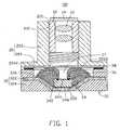
- FIG. 1is a schematic, cross-sectional view of a digital camera module with an image sensor chip package according to a preferred embodiment
- FIG. 2is a schematic, top-down plan view of the leadframe of FIG. 1 ;
- FIG. 3is a cross-sectional view of the leadframe in FIG. 2 along a line III-III;
- FIG. 4is a schematic, top view of the carrier formed by insert-molding shown in FIG. 4 ;
- FIG. 5is a cross-sectional view after the image sensor is put into the carrier
- FIG. 6is a cross-sectional view showing the adhesive glue surrounding all of the bonding wires
- FIG. 7is a cross-sectional view showing the adhesive glue fixing the cover and defining a small sealing space to seal the photosensitive area;
- FIG. 8is a cross-sectional view showing therim of the image sensor package
- FIG. 9is a cross-sectional view showing the barrel and the seat mounted on the image sensor package.
- FIG. 10is a schematic, cross-sectional view of a typical image sensor chip package.
- a digital camera moduleincludes a barrel 10 , a seat 20 and an image sensor chip package 30 in accordance with a preferred embodiment.
- the image sensor chip package 30includes a carrier 32 , a chip 34 , a number of bonding wires 36 and a cover 38 .
- the barrel 10is substantially a hollow cylinder with two open ends so that light can be transmitted therethrough.
- Several lens elements 12are disposed in the barrel 10 , and receive incoming light that enters from the outside.
- the barrel 10has an outer thread 102 defined in an outer periphery wall thereof.
- a glass board 14is disposed in front of the lens elements 12 and covers one end of the barrel 10 . As such, the glass board 14 protects the lens elements 12 from being scraped or otherwise abraded and keeps dust from entering the system.
- the seat 20includes a seat body 202 and a flange 204 formed together.
- the seat body 202is a hollow cylinder.
- the flange 204is formed at a bottom end of the seat body 202 .
- the flange 204has a rectangular cavity 2042 defined in a middle thereof opposite to the seat body 202 .
- the rectangular cavity 2042communicates with the seat body 202 so that light can be transmitted therethrough.
- An outer diameter of the seat body 202is smaller than an edge of the flange 204 so that a step is formed at a connection between them.
- An inner periphery wall of the seat body 202defines an inner thread 201 for engaging with the outer thread 102 of the barrel 10 .
- the carrier 32 of the image sensor chip package 30includes a number of conductive pieces 322 and a plastic base 324 .
- the conductive pieces 322are spaced from each other and aligned in parallel, and cooperatively form the carrier 32 when combined with the plastic base 324 .
- the image sensor chip 34is received in the carrier 32 , and is adhered to the bottom of the carrier 32 with an adhesive glue 346 .
- a top surface of the image sensor chip 34is arranged with a photosensitive area 344 and a number of chip pads 342 around the photosensitive area 344 .
- the bonding wires 36can be made of a conductive material such as, for example, gold or aluminum alloy. One end of each wire 36 is connected/joined with a respective chip pad 342 of the image sensor chip 34 , and the other end of the wire 36 is connected/joined with a respective upper pad 326 forming by the conductive pieces 322 .
- the cover 38is transparent and is laid over the image sensor chip 34 which receives light transmitted through the cover 38 .
- the cover 38is adhered to the base 324 by glue (not labeled) and therefore seals the image sensor chip 34 in the cavity of the base 324 .
- An adhesive glue 3262such as a silicone, epoxy, acrylic, or polyamide adhesive, is applied around the photosensitive area 344 of the image sensor chip 34 .
- the adhesive glue 3262surrounds all of the bonding wires 36 and covers the first portions 3220 , and the inner surface of the carrier 32 .
- the adhesive glue 3262also fixes the cover 38 and defines a small sealing space 37 configured to seal the photosensitive area 344 therein.
- the bonding wires 36 and the adhesive glue 3262are received in the carrier 32 . It can be seen that the photosensitive area 344 of the image sensor chip 34 is sufficiently protected from outside pollution due to the small volume of the sealing space 37 .
- the bonding wires 36are protected by the adhesive glue 3262 , and the conductive pieces 322 are protected by the base 324 .
- a method of fabricating the digital camera module 100is disclosed by way of example.
- a plurality of image sensor packages 30are fabricated simultaneously to minimize the cost associated with each individual image sensor package 30 .
- a conductor element 302is provided.
- the conductor element 320is formed on a metal plate by etching.
- the conductor element 321includes a support beam 321 , many groups of conductive pieces 322 and a number of separate beams 323 .
- the conductive pieces 322are punched so that each of the conductive pieces 322 forms a first terminal portion 3220 , a second connecting portion 3222 and a third terminal portion 3224 , where the second connecting portion 3222 interconnects the first and third terminal portions 3220 , 3224 .
- the first and third portions 3220 , 3224are spaced apart and aligned in parallel to each other.
- the second portion 3222is slanted relative to the first and third portions 3220 , 3224 .
- the conductive pieces 322are divided into two groups. The two groups are symmetrically arranged and the conductive pieces in the same group are parallel to and spaced from each other, thereby forming a plurality of leadframes 320 connected to each other.
- the molten plasticis injected into the conductor element 302 by insert-molding.
- the plasticis solidified to form the plastic base 324 .
- the plastic base 324partially encloses the upper and lower surfaces of each of the leadframes 320 .
- One end of each of the first portions 3220is exposed, thus forming a plurality of upper pads 326 .
- a distal end of each of the third portions 3224is exposed, thus forming a number of lower pads 328 .
- the plastic base 324 and each leadframe 130cooperatively form carriers connected to each other.
- Each carrier 32is formed with a trapezoidal cavity.
- each image sensor chip 34is received in a corresponding trapezoidal cavity, and is adhered to the bottom of the carrier 32 via an adhesive glue 346 .
- the adhesive glue 346can be replaced by any other appropriate adhesive means such as, for example, by metallurgical means.
- each wire 36is connected/joined with a respective chip pad 342 of the image sensor chip 34 , and the other end of the wire 36 is connected/joined with a respective upper pad 326 forming by the first portions 3220 of the leadframe 320 .
- each cover 38is laid over the image sensor chip 34 which receives light transmitted through the cover 38 .
- the cover 38is adhered on the base 324 by glue (not labeled) and therefore seals the image sensor chip 34 in the cavity of the base 324 .
- the adhesive glue 3262surrounds all of the bonding wires 36 and covers the first portions 3220 , and the inner surface of the carrier 32 .
- the adhesive glue 3262also fixes the cover 38 and defines a small sealing space 37 configured to seal the photosensitive area 344 therein.
- the bonding wires 36 and the adhesive glue 3262are received in the carrier 32 . It can be seen that the photosensitive area 344 of the image sensor chip 34 is protected from outside pollution due to the small volume of the sealing space 37 .
- the bonding wires 36are protected by the adhesive glue 3262 , and the leadframe 320 is protected by the base 324 .
- the conductor element 302 with the plastic baseare cut along the rim of each carrier 30 so as to separate a plurality of carriers 30 .
- distal ends of each of the conductive pieces 322are exposed outside.
- the conductive pieces 322are shortened owing to a different shrinkage after the carriers are cut.
- a kind of fuse technologysuch as ultrasonic fuse, laser fuse or heat fuse may be used to irradiate the rim of the carrier. Accordingly, the plastic base 324 are melted so as to enclose the conductive pieces 322 .
- FIG. 9several lens elements 12 are received in the barrel 10 .
- the outer thread 102 of the barrel 10engages with the inner thread 201 of the seat 20 , whereby the barrel 10 and the seat 20 are connected with each other.
- the seat 20is then mounted on the image sensor chip package 30 by welding/glue, with the image sensor 34 aligning with the lens elements 12 .
- the cover 38is received in the rectangular cavity 2042 . The assembly process of the digital camera module 100 is thus completed.
- the arrangement of the conductive pieces of the leadframe 320can be changed so long as the conductive pieces 322 are spaced from each other.
- the second portion 3222can be perpendicular to the first and third portions 3220 , 3224 rather than being slanted.
- the base 324can be of another shape such as cylinder-shaped, or column-shaped with a pentagonal or hexagonal cross-section. Understandably, the image sensor package may also be produced in single units.
- the adhesive glue 3262may only be disposed around the photosensitive area 344 so as to define a sealing space for protecting the photosensitive area 344 .
- One main advantage of the digital cameral module with this image sensor chip packageis its reliability and high image quality.
Landscapes
- Transforming Light Signals Into Electric Signals (AREA)
- Solid State Image Pick-Up Elements (AREA)
Abstract
Description
- This application is related to a co-pending U.S. Patent Application (Attorney Docket No.US7596), entitled “IMAGE SENSOR CHIP PACKAGE FABRICATION METHOD”, by Steven Webster et al. Such application has the same assignee as the present application and has been concurrently filed herewith. The disclosure of the above identified application is incorporated herein by reference.
- The present invention generally relates to an integrated circuit (IC) chip package fabrication method and, more particularly, to a digital camera module fabrication method with an image sensor chip package.
- With the development of wireless communication technologies, increasing numbers of mobile phones and personal digital assistants (PDAs) now include digital cameras as a special feature. Image sensors are a core element of digital cameras. Therefore, image sensors are widely used in digital camera modules in order to convert the optical image data of an object into electrical signals. In order to protect the image sensor from contamination or pollution (i.e. from dust or water vapor), the image sensor is generally sealed in a structural package.
- A typical image sensor chip package method (not labeled) is disclosed in Chinese Publication Number CN1518079 on Aug. 4, 2004, and is illustrated in
FIG. 10 . The image sensor chip package method includes the following steps: firstly, a plurality of [-shaped conductors 130 are provided. Secondly, plastics are injected to partially enclose theconductors 130, thereby forming abase 146. Some of theconductors 130 are exposed outside of thebase 146. Thirdly, a ring-like middle portion 148 is further formed on thebase 146 by means of injection. Thebase 146 and themiddle portion 148 cooperatively form aspace 150. Fourthly, animage sensor 152 having a plurality ofpads 154 is disposed in thespace 150. Fifthly, a number ofbonding wires 156 are provided to connect thepads 154 and theconductors 130. Finally, acover 158 is secured to the top of themiddle portion 148 via an adhesive glue, thereby hermetically sealing thespace 150 and allowing light beams to pass therethrough. - In the process of connecting the
wires 156, eachwire 156 needs to be connected with theconductor 130. Furthermore, a larger space is needed in order to conveniently operate. It is obvious that this method of connectingwires 156 is complex and as a result it is also expensive. In addition, the relative large volume of the image sensor chip package results in more dust-particles adhering to thecover 158, the bottom board and the sidewalls of thebase 146. Thus, more dust-particles will drop onto thechip 152. The dust-particles obscure the optical path and produce errors in the image sensing process. Accordingly, the quality and/or reliability of the imagesensor chip package 100 can be affected. Moreover, thebonding wires 156, exposed in thespace 150, lack protection and may thus easily be damaged by dust-particles entering thespace 150. - Therefore, a new digital camera module fabrication method is desired in order to overcome the above-described shortcomings.
- One embodiment of a digital camera module package method includes the steps of:
- providing a carrier including a base and a leadframe, the base having a cavity therein, the leadframe comprising a plurality of conductive pieces, the conductive pieces of the leadframe being embedded in the base and spaced from each other;
- mounting an image sensor chip in the cavity, the image sensor having a photosensitive area;
- providing a plurality of wires, each electrically connecting the image sensor chip and a corresponding one of the conductive pieces of the carrier;
- applying an adhesive means around the image sensor chip and at least partially covering all the wires;
- mounting a transparent cover to the carrier, the adhesive means adhering to the cover and configured in a manner so as to define a sealing space for a photosensitive area of the image sensor chip therein, and the base and the cover allowing one end of the conductive pieces to be exposed out therefrom; and
- mounting a lens module on the cover.
- Other advantages and novel features will become more apparent from the following detailed description when taken in conjunction with the accompanying drawings.
- Many aspects of the present digital camera module package can be better understood with reference to the following drawings. The components in the drawings are not necessarily drawn to scale, the emphasis instead being placed upon clearly illustrating the principles of the image sensor chip package. Moreover, in the drawings, like reference numerals designate corresponding parts throughout the several views.
FIG. 1 is a schematic, cross-sectional view of a digital camera module with an image sensor chip package according to a preferred embodiment;FIG. 2 is a schematic, top-down plan view of the leadframe ofFIG. 1 ;FIG. 3 is a cross-sectional view of the leadframe inFIG. 2 along a line III-III;FIG. 4 is a schematic, top view of the carrier formed by insert-molding shown inFIG. 4 ;FIG. 5 is a cross-sectional view after the image sensor is put into the carrier;FIG. 6 is a cross-sectional view showing the adhesive glue surrounding all of the bonding wires;FIG. 7 is a cross-sectional view showing the adhesive glue fixing the cover and defining a small sealing space to seal the photosensitive area;FIG. 8 is a cross-sectional view showing therim of the image sensor package;FIG. 9 is a cross-sectional view showing the barrel and the seat mounted on the image sensor package;FIG. 10 is a schematic, cross-sectional view of a typical image sensor chip package.- Referring to
FIG. 1 , a digital camera module includes abarrel 10, aseat 20 and an imagesensor chip package 30 in accordance with a preferred embodiment. The imagesensor chip package 30 includes acarrier 32, achip 34, a number ofbonding wires 36 and acover 38. - The
barrel 10 is substantially a hollow cylinder with two open ends so that light can be transmitted therethrough.Several lens elements 12 are disposed in thebarrel 10, and receive incoming light that enters from the outside. Thebarrel 10 has anouter thread 102 defined in an outer periphery wall thereof. Aglass board 14 is disposed in front of thelens elements 12 and covers one end of thebarrel 10. As such, theglass board 14 protects thelens elements 12 from being scraped or otherwise abraded and keeps dust from entering the system. - The
seat 20 includes aseat body 202 and aflange 204 formed together. Theseat body 202 is a hollow cylinder. Theflange 204 is formed at a bottom end of theseat body 202. Theflange 204 has arectangular cavity 2042 defined in a middle thereof opposite to theseat body 202. Therectangular cavity 2042 communicates with theseat body 202 so that light can be transmitted therethrough. An outer diameter of theseat body 202 is smaller than an edge of theflange 204 so that a step is formed at a connection between them. An inner periphery wall of theseat body 202 defines aninner thread 201 for engaging with theouter thread 102 of thebarrel 10. - The
carrier 32 of the imagesensor chip package 30 includes a number ofconductive pieces 322 and aplastic base 324. Theconductive pieces 322 are spaced from each other and aligned in parallel, and cooperatively form thecarrier 32 when combined with theplastic base 324. - The
image sensor chip 34 is received in thecarrier 32, and is adhered to the bottom of thecarrier 32 with an adhesive glue346. A top surface of theimage sensor chip 34 is arranged with aphotosensitive area 344 and a number ofchip pads 342 around thephotosensitive area 344. - The
bonding wires 36 can be made of a conductive material such as, for example, gold or aluminum alloy. One end of eachwire 36 is connected/joined with arespective chip pad 342 of theimage sensor chip 34, and the other end of thewire 36 is connected/joined with a respectiveupper pad 326 forming by theconductive pieces 322. - The
cover 38 is transparent and is laid over theimage sensor chip 34 which receives light transmitted through thecover 38. Thecover 38 is adhered to thebase 324 by glue (not labeled) and therefore seals theimage sensor chip 34 in the cavity of thebase 324. - An
adhesive glue 3262, such as a silicone, epoxy, acrylic, or polyamide adhesive, is applied around thephotosensitive area 344 of theimage sensor chip 34. Theadhesive glue 3262 surrounds all of thebonding wires 36 and covers thefirst portions 3220, and the inner surface of thecarrier 32. Theadhesive glue 3262 also fixes thecover 38 and defines asmall sealing space 37 configured to seal thephotosensitive area 344 therein. Thebonding wires 36 and theadhesive glue 3262 are received in thecarrier 32. It can be seen that thephotosensitive area 344 of theimage sensor chip 34 is sufficiently protected from outside pollution due to the small volume of the sealingspace 37. Thebonding wires 36 are protected by theadhesive glue 3262, and theconductive pieces 322 are protected by thebase 324. - A method of fabricating the
digital camera module 100 is disclosed by way of example. In one embodiment, a plurality of image sensor packages30 are fabricated simultaneously to minimize the cost associated with each individualimage sensor package 30. Referring toFIGS. 2 and 3 , firstly, aconductor element 302 is provided. The conductor element320 is formed on a metal plate by etching. Theconductor element 321 includes asupport beam 321, many groups ofconductive pieces 322 and a number ofseparate beams 323. Theconductive pieces 322 are punched so that each of theconductive pieces 322 forms afirst terminal portion 3220, a second connectingportion 3222 and athird terminal portion 3224, where the second connectingportion 3222 interconnects the first and thirdterminal portions third portions second portion 3222 is slanted relative to the first andthird portions conductive pieces 322 are divided into two groups. The two groups are symmetrically arranged and the conductive pieces in the same group are parallel to and spaced from each other, thereby forming a plurality of leadframes320 connected to each other. - Secondly, the molten plastic is injected into the
conductor element 302 by insert-molding. The plastic is solidified to form theplastic base 324. Theplastic base 324 partially encloses the upper and lower surfaces of each of the leadframes320. One end of each of thefirst portions 3220 is exposed, thus forming a plurality ofupper pads 326. A distal end of each of thethird portions 3224 is exposed, thus forming a number of lower pads328. Theplastic base 324 and eachleadframe 130 cooperatively form carriers connected to each other. Eachcarrier 32 is formed with a trapezoidal cavity. - Thirdly, referring to
FIG. 5 , eachimage sensor chip 34 is received in a corresponding trapezoidal cavity, and is adhered to the bottom of thecarrier 32 via an adhesive glue346. Alternatively, the adhesive glue346 can be replaced by any other appropriate adhesive means such as, for example, by metallurgical means. - Fourthly, referring to
FIG. 6 , one end of eachwire 36 is connected/joined with arespective chip pad 342 of theimage sensor chip 34, and the other end of thewire 36 is connected/joined with a respectiveupper pad 326 forming by thefirst portions 3220 of the leadframe320. - Fifthly, referring to
FIGS. 7 and 8 , each cover38 is laid over theimage sensor chip 34 which receives light transmitted through thecover 38. Thecover 38 is adhered on thebase 324 by glue (not labeled) and therefore seals theimage sensor chip 34 in the cavity of thebase 324. Theadhesive glue 3262 surrounds all of thebonding wires 36 and covers thefirst portions 3220, and the inner surface of thecarrier 32. Theadhesive glue 3262 also fixes thecover 38 and defines asmall sealing space 37 configured to seal thephotosensitive area 344 therein. Thebonding wires 36 and theadhesive glue 3262 are received in thecarrier 32. It can be seen that thephotosensitive area 344 of theimage sensor chip 34 is protected from outside pollution due to the small volume of the sealingspace 37. Thebonding wires 36 are protected by theadhesive glue 3262, and the leadframe320 is protected by thebase 324. - After that, the
conductor element 302 with the plastic base are cut along the rim of eachcarrier 30 so as to separate a plurality ofcarriers 30. At that time, distal ends of each of theconductive pieces 322 are exposed outside. Usually, theconductive pieces 322 are shortened owing to a different shrinkage after the carriers are cut. A kind of fuse technology such as ultrasonic fuse, laser fuse or heat fuse may be used to irradiate the rim of the carrier. Accordingly, theplastic base 324 are melted so as to enclose theconductive pieces 322. By forming a plurality of image sensor packages30 simultaneously, several advantages are realized. One advantage is that it is less labor intensive to handle and process a plurality of image sensor packages simultaneously rather than to handle and process each image sensor package on an individual base. By reducing labor, the cost associated with each package is minimized. - Finally, referring to
FIG. 9 ,several lens elements 12 are received in thebarrel 10. Theouter thread 102 of thebarrel 10 engages with theinner thread 201 of theseat 20, whereby thebarrel 10 and theseat 20 are connected with each other. Theseat 20 is then mounted on the imagesensor chip package 30 by welding/glue, with theimage sensor 34 aligning with thelens elements 12. At the same time, thecover 38 is received in therectangular cavity 2042. The assembly process of thedigital camera module 100 is thus completed. - In an alternative embodiment, the arrangement of the conductive pieces of the leadframe320 can be changed so long as the
conductive pieces 322 are spaced from each other. Thesecond portion 3222 can be perpendicular to the first andthird portions - In the above embodiments, the
adhesive glue 3262 may only be disposed around thephotosensitive area 344 so as to define a sealing space for protecting thephotosensitive area 344. One main advantage of the digital cameral module with this image sensor chip package is its reliability and high image quality. - It is believed that the present embodiments and their advantages will be understood from the foregoing description, and it will be apparent that various changes may be made thereto without departing from the spirit and scope of the invention or sacrificing all of its material advantages, the examples hereinbefore described merely being preferred or exemplary embodiments of the invention.
Claims (14)
Applications Claiming Priority (2)
| Application Number | Priority Date | Filing Date | Title |
|---|---|---|---|
| CNB200510037226XACN100483655C (en) | 2005-09-09 | 2005-09-09 | Producing process for digital camera module |
| CN200510037226.X | 2005-09-09 |
Publications (2)
| Publication Number | Publication Date |
|---|---|
| US20070057148A1true US20070057148A1 (en) | 2007-03-15 |
| US7342215B2 US7342215B2 (en) | 2008-03-11 |
Family
ID=37854125
Family Applications (1)
| Application Number | Title | Priority Date | Filing Date |
|---|---|---|---|
| US11/453,454ActiveUS7342215B2 (en) | 2005-09-09 | 2006-06-14 | Digital camera module package fabrication method |
Country Status (2)
| Country | Link |
|---|---|
| US (1) | US7342215B2 (en) |
| CN (1) | CN100483655C (en) |
Cited By (3)
| Publication number | Priority date | Publication date | Assignee | Title |
|---|---|---|---|---|
| US20080252771A1 (en)* | 2007-04-13 | 2008-10-16 | Hon Hai Precision Industry Co., Ltd. | Camera module with compact packaging of image sensor chip and method of manufacturing the same |
| US20210392251A1 (en)* | 2016-02-18 | 2021-12-16 | Ningbo Sunny Opotech Co., Ltd. | Integral Parking Process-Based Camera Module, Integral Base Component of Same, and Manufacturing Method Thereof |
| US20240171841A1 (en)* | 2021-08-03 | 2024-05-23 | Shenzhen Jsl Electronics Corporation Limited | Camera module, image acquisition module, and processing method for base of image acquisition module |
Families Citing this family (5)
| Publication number | Priority date | Publication date | Assignee | Title |
|---|---|---|---|---|
| CN100546026C (en)* | 2007-04-29 | 2009-09-30 | 鸿富锦精密工业(深圳)有限公司 | image capture device |
| CN105612666B (en)* | 2014-06-20 | 2018-04-24 | 深圳市大富科技股份有限公司 | Cavity Filter and Connector Components |
| CN105721754B (en)* | 2016-04-01 | 2020-04-28 | 宁波舜宇光电信息有限公司 | Camera module based on integrated packaging process |
| EP3707750B1 (en)* | 2017-11-07 | 2024-12-04 | AMS Sensors Singapore Pte. Ltd. | Optoelectronic modules having locking assemblies and methods for manufacturing the same |
| CN110794640A (en)* | 2018-08-01 | 2020-02-14 | 三赢科技(深圳)有限公司 | 3D projector |
Citations (11)
| Publication number | Priority date | Publication date | Assignee | Title |
|---|---|---|---|---|
| US5159432A (en)* | 1988-12-26 | 1992-10-27 | Sumitomo Electric Industries, Ltd. | Semiconductor device package having improved sealing at the aluminum nitride substrate/low melting point glass interface |
| US5877546A (en)* | 1996-01-02 | 1999-03-02 | Lg Semicon Co., Ltd. | Semiconductor package with transparent window and fabrication method thereof |
| US5950074A (en)* | 1997-04-18 | 1999-09-07 | Amkor Technology, Inc. | Method of making an integrated circuit package |
| US6384472B1 (en)* | 2000-03-24 | 2002-05-07 | Siliconware Precision Industries Co., Ltd | Leadless image sensor package structure and method for making the same |
| US6420204B2 (en)* | 1999-06-03 | 2002-07-16 | Amkor Technology, Inc. | Method of making a plastic package for an optical integrated circuit device |
| US6630727B1 (en)* | 1998-03-03 | 2003-10-07 | Infineon Technologies Ag | Modularly expandable multi-layered semiconductor component |
| US6686588B1 (en)* | 2001-01-16 | 2004-02-03 | Amkor Technology, Inc. | Optical module with lens integral holder |
| US20040041088A1 (en)* | 2002-08-27 | 2004-03-04 | Chen Shu Fen | Digital CMOS sensor |
| US6759266B1 (en)* | 2001-09-04 | 2004-07-06 | Amkor Technology, Inc. | Quick sealing glass-lidded package fabrication method |
| US20040165356A1 (en)* | 2003-02-24 | 2004-08-26 | Mun Lee Sai | Leadless leadframe electronic package and sensor module incorporating same |
| US20050258518A1 (en)* | 2004-05-24 | 2005-11-24 | Advanced Semiconductor Engineering Inc. | Image sensor package module with a leadless leadframe between chips |
Family Cites Families (3)
| Publication number | Priority date | Publication date | Assignee | Title |
|---|---|---|---|---|
| CN1508879A (en)* | 2002-12-20 | 2004-06-30 | 胜开科技股份有限公司 | Injection-molded image sensor and manufacturing method thereof |
| CN1450651A (en)* | 2003-05-15 | 2003-10-22 | 王鸿仁 | Image sensor packaging structure and image capture module using the image sensor |
| CN100350621C (en)* | 2003-06-03 | 2007-11-21 | 胜开科技股份有限公司 | Image sensor module and manufacturing method thereof |
- 2005
- 2005-09-09CNCNB200510037226XApatent/CN100483655C/ennot_activeExpired - Fee Related
- 2006
- 2006-06-14USUS11/453,454patent/US7342215B2/enactiveActive
Patent Citations (13)
| Publication number | Priority date | Publication date | Assignee | Title |
|---|---|---|---|---|
| US5159432A (en)* | 1988-12-26 | 1992-10-27 | Sumitomo Electric Industries, Ltd. | Semiconductor device package having improved sealing at the aluminum nitride substrate/low melting point glass interface |
| US5877546A (en)* | 1996-01-02 | 1999-03-02 | Lg Semicon Co., Ltd. | Semiconductor package with transparent window and fabrication method thereof |
| US5950074A (en)* | 1997-04-18 | 1999-09-07 | Amkor Technology, Inc. | Method of making an integrated circuit package |
| US6034429A (en)* | 1997-04-18 | 2000-03-07 | Amkor Technology, Inc. | Integrated circuit package |
| US6630727B1 (en)* | 1998-03-03 | 2003-10-07 | Infineon Technologies Ag | Modularly expandable multi-layered semiconductor component |
| US6420204B2 (en)* | 1999-06-03 | 2002-07-16 | Amkor Technology, Inc. | Method of making a plastic package for an optical integrated circuit device |
| US6384472B1 (en)* | 2000-03-24 | 2002-05-07 | Siliconware Precision Industries Co., Ltd | Leadless image sensor package structure and method for making the same |
| US6686588B1 (en)* | 2001-01-16 | 2004-02-03 | Amkor Technology, Inc. | Optical module with lens integral holder |
| US6759266B1 (en)* | 2001-09-04 | 2004-07-06 | Amkor Technology, Inc. | Quick sealing glass-lidded package fabrication method |
| US20040041088A1 (en)* | 2002-08-27 | 2004-03-04 | Chen Shu Fen | Digital CMOS sensor |
| US20040165356A1 (en)* | 2003-02-24 | 2004-08-26 | Mun Lee Sai | Leadless leadframe electronic package and sensor module incorporating same |
| US7095621B2 (en)* | 2003-02-24 | 2006-08-22 | Avago Technologies Sensor Ip (Singapore) Pte. Ltd. | Leadless leadframe electronic package and sensor module incorporating same |
| US20050258518A1 (en)* | 2004-05-24 | 2005-11-24 | Advanced Semiconductor Engineering Inc. | Image sensor package module with a leadless leadframe between chips |
Cited By (4)
| Publication number | Priority date | Publication date | Assignee | Title |
|---|---|---|---|---|
| US20080252771A1 (en)* | 2007-04-13 | 2008-10-16 | Hon Hai Precision Industry Co., Ltd. | Camera module with compact packaging of image sensor chip and method of manufacturing the same |
| US20210392251A1 (en)* | 2016-02-18 | 2021-12-16 | Ningbo Sunny Opotech Co., Ltd. | Integral Parking Process-Based Camera Module, Integral Base Component of Same, and Manufacturing Method Thereof |
| US11877044B2 (en)* | 2016-02-18 | 2024-01-16 | Ningbo Sunny Opotech Co., Ltd. | Integral packaging process-based camera module, integral base component of same, and manufacturing method thereof |
| US20240171841A1 (en)* | 2021-08-03 | 2024-05-23 | Shenzhen Jsl Electronics Corporation Limited | Camera module, image acquisition module, and processing method for base of image acquisition module |
Also Published As
| Publication number | Publication date |
|---|---|
| US7342215B2 (en) | 2008-03-11 |
| CN100483655C (en) | 2009-04-29 |
| CN1929103A (en) | 2007-03-14 |
Similar Documents
| Publication | Publication Date | Title |
|---|---|---|
| US7646429B2 (en) | Digital camera module packaging method | |
| US7342215B2 (en) | Digital camera module package fabrication method | |
| US7554184B2 (en) | Image sensor chip package | |
| US7595839B2 (en) | Image sensor chip packaging method | |
| KR100604190B1 (en) | Solid state imaging device, semiconductor wafer, optical device module, method of solid state imaging device fabrication, and method of optical device module fabrication | |
| US8164676B2 (en) | Camera module providing reliable long term adherence | |
| US7643081B2 (en) | Digital camera module with small sized image sensor chip package | |
| US7521770B2 (en) | Image capturing device | |
| US7408205B2 (en) | Digital camera module | |
| US20080246845A1 (en) | Camera module with compact packaging of image sensor chip | |
| US20080303939A1 (en) | Camera module with compact packaging of image sensor chip | |
| US20070034772A1 (en) | Image sensor chip package | |
| US20080252771A1 (en) | Camera module with compact packaging of image sensor chip and method of manufacturing the same | |
| US20050073036A1 (en) | Overmolded optical package | |
| US20070108561A1 (en) | Image sensor chip package | |
| US7638864B2 (en) | Chip package, method of making same and digital camera module using the package | |
| KR20180132684A (en) | Camera module, its photosensitive part and method of manufacturing the same | |
| CN101310381A (en) | Semiconductor package and manufacturing method thereof, semiconductor module and electronic device | |
| KR101579623B1 (en) | Semiconductor package for image sensor and manufacturing method thereof | |
| US6876544B2 (en) | Image sensor module and method for manufacturing the same | |
| EP3748948B1 (en) | Camera module, camera module assembly method and mobile terminal | |
| US20080203512A1 (en) | Image sensor chip package | |
| US7592197B2 (en) | Image sensor chip package fabrication method | |
| US20060273249A1 (en) | Image sensor chip package and method of manufacturing the same | |
| CN101299432A (en) | Optical device and method of manufacturing the same |
Legal Events
| Date | Code | Title | Description |
|---|---|---|---|
| AS | Assignment | Owner name:ALTUS TECHNOLOGY INC., TAIWAN Free format text:ASSIGNMENT OF ASSIGNORS INTEREST;ASSIGNORS:WEBSTER, STEVEN;WU, YING-CHENG;LIU, KUN-HSIEH;REEL/FRAME:017981/0613 Effective date:20060608 | |
| STCF | Information on status: patent grant | Free format text:PATENTED CASE | |
| FPAY | Fee payment | Year of fee payment:4 | |
| AS | Assignment | Owner name:HON HAI PRECISION INDUSTRY CO., LTD., TAIWAN Free format text:ASSIGNMENT OF ASSIGNORS INTEREST;ASSIGNOR:ALTUS TECHNOLOGY INC.;REEL/FRAME:029127/0387 Effective date:20120928 | |
| FPAY | Fee payment | Year of fee payment:8 | |
| AS | Assignment | Owner name:POLIGHT TECHNOLOGIES LTD., TAIWAN Free format text:ASSIGNMENT OF ASSIGNORS INTEREST;ASSIGNOR:HON HAI PRECISION INDUSTRY CO., LTD.;REEL/FRAME:050248/0298 Effective date:20190514 | |
| MAFP | Maintenance fee payment | Free format text:PAYMENT OF MAINTENANCE FEE, 12TH YEAR, LARGE ENTITY (ORIGINAL EVENT CODE: M1553); ENTITY STATUS OF PATENT OWNER: LARGE ENTITY Year of fee payment:12 |