US20070051997A1 - Semiconductor memory device - Google Patents
Semiconductor memory deviceDownload PDFInfo
- Publication number
- US20070051997A1 US20070051997A1US11/218,184US21818405AUS2007051997A1US 20070051997 A1US20070051997 A1US 20070051997A1US 21818405 AUS21818405 AUS 21818405AUS 2007051997 A1US2007051997 A1US 2007051997A1
- Authority
- US
- United States
- Prior art keywords
- source
- semiconductor substrate
- memory device
- gate
- recessed
- Prior art date
- Legal status (The legal status is an assumption and is not a legal conclusion. Google has not performed a legal analysis and makes no representation as to the accuracy of the status listed.)
- Granted
Links
Images


Classifications
- H—ELECTRICITY
- H10—SEMICONDUCTOR DEVICES; ELECTRIC SOLID-STATE DEVICES NOT OTHERWISE PROVIDED FOR
- H10B—ELECTRONIC MEMORY DEVICES
- H10B12/00—Dynamic random access memory [DRAM] devices
- H10B12/01—Manufacture or treatment
- H10B12/02—Manufacture or treatment for one transistor one-capacitor [1T-1C] memory cells
- H10B12/05—Making the transistor
- H10B12/053—Making the transistor the transistor being at least partially in a trench in the substrate
- H—ELECTRICITY
- H10—SEMICONDUCTOR DEVICES; ELECTRIC SOLID-STATE DEVICES NOT OTHERWISE PROVIDED FOR
- H10D—INORGANIC ELECTRIC SEMICONDUCTOR DEVICES
- H10D84/00—Integrated devices formed in or on semiconductor substrates that comprise only semiconducting layers, e.g. on Si wafers or on GaAs-on-Si wafers
- H10D84/01—Manufacture or treatment
- H10D84/0123—Integrating together multiple components covered by H10D12/00 or H10D30/00, e.g. integrating multiple IGBTs
- H10D84/0126—Integrating together multiple components covered by H10D12/00 or H10D30/00, e.g. integrating multiple IGBTs the components including insulated gates, e.g. IGFETs
- H10D84/016—Integrating together multiple components covered by H10D12/00 or H10D30/00, e.g. integrating multiple IGBTs the components including insulated gates, e.g. IGFETs the components including vertical IGFETs
- H—ELECTRICITY
- H10—SEMICONDUCTOR DEVICES; ELECTRIC SOLID-STATE DEVICES NOT OTHERWISE PROVIDED FOR
- H10D—INORGANIC ELECTRIC SEMICONDUCTOR DEVICES
- H10D84/00—Integrated devices formed in or on semiconductor substrates that comprise only semiconducting layers, e.g. on Si wafers or on GaAs-on-Si wafers
- H10D84/01—Manufacture or treatment
- H10D84/02—Manufacture or treatment characterised by using material-based technologies
- H10D84/03—Manufacture or treatment characterised by using material-based technologies using Group IV technology, e.g. silicon technology or silicon-carbide [SiC] technology
- H10D84/038—Manufacture or treatment characterised by using material-based technologies using Group IV technology, e.g. silicon technology or silicon-carbide [SiC] technology using silicon technology, e.g. SiGe
- H—ELECTRICITY
- H10—SEMICONDUCTOR DEVICES; ELECTRIC SOLID-STATE DEVICES NOT OTHERWISE PROVIDED FOR
- H10B—ELECTRONIC MEMORY DEVICES
- H10B12/00—Dynamic random access memory [DRAM] devices
- H10B12/30—DRAM devices comprising one-transistor - one-capacitor [1T-1C] memory cells
- H10B12/31—DRAM devices comprising one-transistor - one-capacitor [1T-1C] memory cells having a storage electrode stacked over the transistor
- H10B12/318—DRAM devices comprising one-transistor - one-capacitor [1T-1C] memory cells having a storage electrode stacked over the transistor the storage electrode having multiple segments
- H—ELECTRICITY
- H10—SEMICONDUCTOR DEVICES; ELECTRIC SOLID-STATE DEVICES NOT OTHERWISE PROVIDED FOR
- H10B—ELECTRONIC MEMORY DEVICES
- H10B12/00—Dynamic random access memory [DRAM] devices
- H10B12/30—DRAM devices comprising one-transistor - one-capacitor [1T-1C] memory cells
- H10B12/34—DRAM devices comprising one-transistor - one-capacitor [1T-1C] memory cells the transistor being at least partially in a trench in the substrate
- H—ELECTRICITY
- H10—SEMICONDUCTOR DEVICES; ELECTRIC SOLID-STATE DEVICES NOT OTHERWISE PROVIDED FOR
- H10B—ELECTRONIC MEMORY DEVICES
- H10B12/00—Dynamic random access memory [DRAM] devices
- H10B12/30—DRAM devices comprising one-transistor - one-capacitor [1T-1C] memory cells
- H10B12/48—Data lines or contacts therefor
- H10B12/485—Bit line contacts
Definitions
- This inventionrelates to microelectronic devices and related fabrication methods. More particularly, this invention relates to a memory device having a digit line that is directly coupled to a transistor source.
- DRAMDynamic Random Access Memory
- RAMsemiconductor Random Access Memory
- a DRAM celltypically comprises a charge storage capacitor (or cell capacitor) coupled to an access device, such as a Metal-Oxide-Semiconductor Field Effect Transistor (MOSFET, or simply FET).
- MOSFETMetal-Oxide-Semiconductor Field Effect Transistor
- These access devicesfunctions to apply or remove charge on the capacitor, thus affecting a logical state defined by the stored charge.
- the amount of charge stored on the capacitoris determined by the electrode (or storage node) area and the interelectrode spacing.
- the conditions of DRAM operationsuch as operating voltage, leakage rate and refresh rate, will generally mandate that a certain minimum charge be stored by the capacitor.
- FETsare widely used in integrated circuit devices including logic, memory and/or microprocessor devices that are used in consumer and/or industrial applications. As the integration density of integrated circuit FETs continues to increase, it may be desirable to continue to shrink the dimensions of the FETs.
- features of integrated circuit FETsmay be formed on a microelectronic substrate, such as silicon semiconductor substrate, using photolithography and etching. As the minimum feature size is reduced, conventional fabrication techniques must also evolve in order to accurately fabricate the reduced size features.
- fabrication of memory devicesmay be improved by reducing the number of processing steps involved in the fabrication process.
- improved transistor and charge storage devicesmay also decrease the manufacturing complexity, while maintaining or increasing the accuracy of the manufacturing process.
- a memory devicecomprising a vertical transistor includes a digit line that is directly coupled to the source regions of each memory cell.
- an electrical plugis deposited on an upper surface of the source regions and the digit line is electrically coupled to the electrical plug.
- a memory devicecomprising a vertical transistor includes gate regions that are recessed from an upper portion of a silicon substrate. With the gate regions recessed from the silicon substrate, the gate regions are spaced further from the source/drain regions and then in prior art vertical transistors and, accordingly, cross capacitance between the gate regions and the source/drain regions is reduced. By reducing cross capacitance between the gate region and the source/drain regions, the improved memory device design may increase accuracy of the memory device. Exemplary methods for fabricating a memory device having a recessed gate region are described below with respect to the figures.
- a memory devicecomprises a semiconductor substrate having a first surface, a recessed gate formed in the substrate and defining a first and second lateral sides, a first source/drain region formed on the first surface of the semiconductor substrate adjacent the first lateral side of the recessed gate, a second source/drain region formed on the first surface of the semiconductor substrate adjacent the second lateral side of the recessed gate, wherein application of a voltage to the recessed gate results in formation of a conductive channel between the first and second source/drain regions along a path that is recessed into the semiconductor substrate, a charge storage device formed above the semiconductor substrate, wherein the charge storage device is electrically coupled to the first source/drain region, and a conductive data line interposed between the charge storage device and the first surface of the semiconductor substrate wherein the conductive data line comprises a first portion that extends at a first height above the first surface of the semiconductor substrate and a second portion that extends downward from the first portion to electrically contact the second source/drain region, and wherein the first and second portions
- a method of fabricating a memory devicecomprises forming a semiconductor substrate having a first surface, forming a recessed gate in the substrate, wherein the recessed gate defines a first and second lateral sides, forming a first source/drain region on the first surface of the semiconductor substrate adjacent a first lateral side of the recessed gate, forming a second source/drain region on the first surface of the semiconductor substrate adjacent a second lateral side of the recessed gate, wherein application of a voltage to the gate results in the formation of a conductive channel between the first and second source/drain regions along a path that is recessed into the semiconductor substrate, forming a conductive data line between the charge storage device and the first surface of the semiconductor substrate, wherein the conductive data line comprises a first portion that extends a first height above the first surface of the semiconductor substrate and a second portion that extends downward from the first portion to electrically contact the second source/drain region, and wherein the first and second portions are formed of the same material, and forming a charge storage
- a memory devicecomprises a semiconductor substrate, a vertically extending gate region recessed in the substrate, a source region positioned on a first side of the gate, the source region being formed at least partially in the semiconductor substrate, a drain region positioned on a second side of the gate, wherein the second side is opposite the first side, and a digit line contact directly electrically connected to the source region and directly electrically connected to a digit line contact of the memory device.
- a memory devicecomprises a source region, a drain region, a gate region separating the source and drain regions, and means for directly electrically coupling a digit line electrode of the memory device to the source region.
- a memory arraycomprises a plurality of memory cells.
- the arraycomprises a semiconductor substrate having a first surface, a plurality of recessed gates formed in the substrate, each defining respective first and second lateral sides, a plurality of first source/drain regions formed on the first surface of the semiconductor substrate adjacent respective first lateral sides of each recessed gate, a plurality of second source/drain regions formed on the first surface of the semiconductor substrate adjacent respective second lateral sides of each recessed gate, wherein application of a voltage to each gate results in the formation of a conductive channel between the respective first and second source/drain regions on either side of the gate along a path that is recessed into the semiconductor substrate, a plurality of charge storage devices formed above the semiconductor substrate, wherein the charge storage devices are electrically coupled to respective first source/drain regions, and a plurality of conductive data lines interposed between each the charge storage devices and the first surface of the semiconductor substrate.
- the conductive data lineseach comprise a first portion that extends at a first height
- a memory devicecomprises a semiconductor substrate having a first surface, a recessed gate that is formed in the substrate so as to be spaced a first distance from the first surface, wherein the recessed gate defines a first and second lateral sides, a first source/drain region formed on the first surface of the semiconductor substrate adjacent a first lateral side of the recessed gate, a second source/drain region formed on the first surface of the semiconductor substrate adjacent a second lateral side of the recessed gate wherein the application of voltage to the gate results in the formation of a conductive channel between the first and second source/drain regions along a path that is recessed into the semiconductor substrate and wherein the first distance is selected such that the gate structure is substantially located below the first and second source/drain regions so as to reduce the cross-capacitance between the gate and the first and second source/drain regions, a charge storage device formed above the semiconductor substrate wherein the charge storage device is electrically coupled to the first source/drain region, and a conductive data line interposed between the charge storage device
- a memory devicecomprises a semiconductor substrate having a top surface, an active area positioned on a first side of the gate, the active area being formed in the semiconductor substrate, and a vertically extending gate positioned proximate the active area, wherein a top surface of the gate is elevationally below the top surface of the semiconductor substrate.
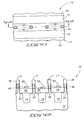
- FIG. 1is a top view of a portion of a memory device at an initial processing stage.
- FIG. 2is a cross-sectional view taken a long line 2 - 2 of FIG. 1 .
- FIG. 3is a top view of the memory device illustrated in FIG. 1 at a subsequent processing stage.
- FIG. 4is a cross-sectional view of the memory device illustrated in FIG. 1 at a subsequent processing stage.
- FIG. 5is a top view of the memory device 10 at a processing stage subsequent to that of FIG. 3 .
- FIG. 6is a cross-sectional view of the memory device 10 at a processing stage subsequent to that of FIGS. 4 .
- FIG. 7is a top view of the memory device 10 rotated 90° from the embodiment illustrated in FIG. 5 .
- FIG. 8is a cross-sectional view of the memory device 10 rotated 90° from the embodiment illustrated in FIGS. 6 .
- FIG. 9is a top view of the memory device 10 at a processing stage subsequent to that of FIG. 5 .
- FIG. 10is a cross-sectional view of the memory device 10 at a processing stage subsequent to that of FIGS. 6 .
- FIG. 11is a top view of the memory device 10 rotated 90° from the embodiment illustrated in FIG. 9 .
- FIG. 12is a cross-sectional view of the memory device 10 rotated 90° from the embodiment illustrated in FIG. 10 .
- FIG. 13is a top view of the memory device 10 at a processing stage subsequent to that of FIG. 9 .
- FIG. 14is a cross-sectional view of the memory device 10 at a processing stage subsequent to that of FIG. 10 .
- FIG. 15is a top view of the memory device 10 rotated 90° from the embodiment illustrated in FIG. 13 .
- FIG. 16is a cross-sectional view of the memory device 10 rotated 90° from the embodiment illustrated in FIG. 14 .
- FIG. 17is a top view of the memory device 10 at a processing stage subsequent to that of FIG. 13 .
- FIG. 18is a cross-sectional view of the memory device 10 at a processing stage subsequent to that of FIG. 14 .
- FIG. 19is a top view of the memory device 10 rotated 90° from the embodiment illustrated in FIG. 17 .
- FIG. 20is a cross-sectional view of the memory device 10 rotated 90° from the embodiment illustrated in FIG. 18 .
- FIG. 21is a top view of the memory device 10 at a processing stage subsequent to that of FIG. 17 .
- FIG. 22is a cross-sectional view of the memory device 10 at a processing stage subsequent to that of FIG. 18 .
- FIG. 23is a top view of the memory device 10 rotated 90° from the embodiment illustrated in FIG. 21 .
- FIG. 24is a cross-sectional view of the memory device 10 rotated 90° from the embodiment illustrated in FIG. 22 .
- FIG. 25is a top view of the memory device 10 at a processing stage subsequent to that of FIG. 21 .
- FIG. 26is a cross-sectional view of the memory device 10 at a processing stage subsequent to that of FIG. 22 .
- FIG. 27is a top view of the memory device 10 rotated 90° from the embodiment illustrated in FIG. 25 .
- FIG. 28is a cross-sectional view of the memory device 10 rotated 90° from the embodiment illustrated in FIG. 26 .
- FIG. 29is a top view of the memory device 10 at a processing stage subsequent to that of FIG. 25 .
- FIG. 30is a cross-sectional view of the memory device 10 at a processing stage subsequent to that of FIG. 26 .
- FIG. 31is a top view of the memory device 10 rotated 90° from the embodiment illustrated in FIG. 29 .
- FIG. 32is a cross-sectional view of the memory device 10 rotated 90° from the embodiment illustrated in FIG. 30 .
- FIG. 33is a top view of the memory device 10 at a processing stage subsequent to that of FIG. 29 .
- FIG. 34is a cross-sectional view of the memory device 10 at a processing stage subsequent to that of FIG. 30 .
- FIG. 35is a top view of the memory device 10 rotated 90° from the embodiment illustrated in FIG. 33 .
- FIG. 36is a cross-sectional view of the memory device 10 rotated 90° from the embodiment illustrated in FIG. 34 .
- FIG. 37is a top view of the memory device 10 at a processing stage subsequent to that of FIG. 33 .
- FIG. 38is a cross-sectional view of the memory device 10 at a processing stage subsequent to that of FIG. 34 .
- FIG. 39is a top view of the memory device 10 rotated 90° from the embodiment illustrated in FIG. 37 .
- FIG. 40is a cross-sectional view of the memory device 10 rotated 90° from the embodiment illustrated in FIG. 38 .
- FIG. 41is a top view of the memory device 10 at a processing stage subsequent to that of FIG. 37 .
- FIG. 42is a cross-sectional view of the memory device 10 at a processing stage subsequent to that of FIG. 38 .
- FIG. 43is a top view of the memory device 10 rotated 90° from the embodiment illustrated in FIG. 41 .
- FIG. 44is a cross-sectional view of the memory device 10 rotated 90° from the embodiment illustrated in FIG. 42 .
- FIG. 45is a top view of the memory device 10 at a processing stage subsequent to that of FIGS. 41 .
- FIG. 46is a cross-sectional view of the memory device 10 at a processing stage subsequent to that of FIG. 42 .
- FIG. 47is a top view of the memory device 10 rotated 90° from the embodiment illustrated in FIG. 45 .
- FIG. 48is a cross-sectional view of the memory device 10 rotated 90° from the embodiment illustrated in FIG. 46 .
- FIG. 49is a cross-sectional view of the memory device 10 (at the same orientation as FIG. 46 ) at a subsequent processing stage.
- FIG. 50is a cross-sectional view of the memory device 10 (at the same orientation as FIG. 48 ) at a subsequent processing stage.
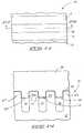
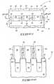
- FIGS. 1 and 2illustrate a semiconductor substrate 12 having shallow trench isolation (STI) regions 14 .
- FIG. 1is a top view of a portion of a memory device 10 at an initial processing stage, wherein the memory device 10 includes the substrate 12 patterned with STI regions 14 and pillars 16 .
- the STI regions 14 and pillars 16alternate in the substrate 12 .
- FIG. 2is a cross-sectional view taken a long line 2 - 2 of FIG. 1 .
- the STI regions 14form pillars 16 in the substrate 12 .
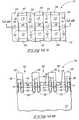
- FIGS. 3 and 4are top and cross-sectional views, respectively, of the memory device 10 at processing stage subsequent to the embodiment illustrated in FIGS. 1 and 2 .
- a nitride layer 18has been deposited on the upper services of the pillars 16 and STI regions 14 .
- the dashed lines in FIG. 3indicate surfaces that are not visible from the top view.
- the pillars 16 and STI regions 14are not visible from the top view illustrated in FIG. 3 , due to the deposition of nitride layer 18 on top of these surfaces.
- the nitride layer 18has a thickness in the range of about 2000 to 3000 Angstroms. In other embodiments, however, the thickness of the nitride layer 18 may be adjusted according to various design parameters.
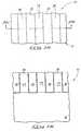
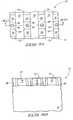
- FIGS. 5-8are views of the memory device 10 at a processing stage subsequent to that of FIGS. 3 and 4 . More particularly, FIGS. 5 and 6 are top and cross-sectional views, respectively, and FIGS. 7 and 8 are top and cross-sectional views, respectively, rotated 90° from the embodiments illustrated in FIGS. 5 and 6 .
- the nitride layer 18has been patterned and etched to form trenches 20 in the nitride layer 18 .
- the trenches 20extend to an upper surface 22 of the substrate 12 .
- the trenches 20also expose isolation region portions 24 of the STI regions 14 . As illustrated in FIG.
- the nitride layer 18is now patterned so that nitride runners 19 extend vertically from the substrate 12 and are generally separated by the trenches 20 and are parallel to one another.
- the upper surface portions 22 of the substrate 12are generally surrounded by the isolation region portions 24 and the nitride layer 18 .
- the upper surface portions 22are generally shaped as squares.
- FIGS. 9-12are views of the memory device 10 at a processing step subsequent to that of FIGS. 5-8 . More particularly, FIGS. 9 and 10 are top and cross-sectional views, respectively, of the memory device 10 and FIGS. 11 and 12 are top and cross-sectional views, respectively, of the memory device 10 rotated 90° from the embodiments illustrated in FIGS. 9 and 10 .
- isolation region portions 24FIG. 6
- the isolation region portions 24are etched using a reactive ion etch (RIE) process to selectively etch the nitride runners 19 .
- RIEreactive ion etch
- the etch processexposes sidewalls 27 of the substrate 12 which were originally covered by an insulative material deposited in the STI regions 14 .
- the recessed surfaces 26are in the range of about 500 to 1500 Angstroms below the upper surface portions 22 of the substrate 12 . In another embodiment, the recessed surfaces 26 are in the range of about 800 to 1200 Angstroms below the upper surface portions 22 of the substrate 12 . In other embodiments, the recessed surfaces 26 may extend other distances below the upper surface portions 22 .
- etching processfor example, residual oxide on the sidewalls 27 and upper surface portions 22 is removed.
- a wet hydrofluoric (HF) etchis used to remove these residual oxides.
- HFwet hydrofluoric
- other clean etchesmay be used in order to achieve similar results.
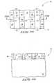
- FIGS. 13-16are views of the memory device 10 at a processing step subsequent to that of FIGS. 9-12 . More particularly, FIGS. 13 and 14 are top and cross-sectional views, respectively, of the memory device 10 and FIGS. 15 and 16 are top and cross-sectional views, respectively, of the memory device 10 rotated 90° from the embodiments illustrated in FIGS. 13 and 14 . As illustrated in FIGS. 14 and 16 , for example, a nitride liner 28 has been deposited on the upper surface 22 of the substrate 12 , the recessed surfaces 26 , and the sidewalls 27 . In one embodiment, the nitride liner 28 has a thickness in the range of about 30 to 100 Angstroms.
- a sacrificial layer 30such as a spin-on-glass (SOG), for example, is deposited in the trenches 20 ( FIG. 12 ) between the nitride runners 19 .
- the sacrificial layermay comprise other materials, such as borophosphorous silica glass (BPSG) and/or TEOS.
- the sacrificial layer 30is etched so that the sacrificial layer 30 is planar with the nitride runners 19 .
- the sacrificial layer 30is removed using a chemical mechanical polishing (CMP) process; however other etching processes may be used in order to adjust a height of the sacrificial layer 30 .
- CMPchemical mechanical polishing
- FIGS. 17-20are views of the memory device 10 at a processing step subsequent to that of FIGS. 13-16 . More particularly, FIGS. 17 and 18 are top and cross-sectional views, respectively, of the memory device 10 and FIGS. 19 and 20 are top and cross-sectional views, respectively, of the memory device 10 rotated 90° from the embodiments illustrated in FIGS. 17 and 18 . As illustrated in FIG. 18 , for example, a portion of the sacrificial layer 30 is selectively etched in order to expose the nitride liner 28 over upper surface portions 22 of substrate 12 . The sacrificial layer 30 is selectively etched so that columns remain extending upward above the STI regions 14 . As shown in FIG.
- the exposed portions of the nitride liner 28 on the upper surface portions 22are removed to expose the upper surface portions 22 of the silicon substrate 12 between the pillars of the sacrificial layer 30 .
- a selective nitride etchis used to etch the nitride liner 28 from the upper surface portions 22 of the substrate 12 .
- openings 31extend to expose the upper surface portions 22 .
- the exposed upper surface portions 22function as active areas for the memory device 10 .
- FIGS. 21-24are views of the memory device 10 at a processing step subsequent to that of FIGS. 17-20 . More particularly, FIGS. 21 and 22 are top and cross-sectional views, respectively, of the memory device 10 and FIGS. 23 and 24 are top and cross-sectional views, respectively, of the memory device 10 rotated 90° from the embodiments illustrated in FIGS. 21 and 22 . As illustrated in FIGS. 21-24 , insulative spacers 34 have been formed on either side of the sacrificial layer 30 (e.g., FIG. 22 ) and the nitride runners 19 (e.g., FIG. 24 ). In one embodiment, the insulative spacers 34 comprise Tetraethyl Orthosilicate (TEOS).
- TEOSTetraethyl Orthosilicate
- a layer of insulative materialis deposited over the silicon substrate 12 in order to fill the openings 31 ( FIG. 18 ).
- the insulative materialis then anisotropically etched to form the sacrificial insulative spacers 34 .
- a reactive ion etchis used to remove portions of the insulative material, leaving only about 200 to 500 Angstroms of material surrounding the nitride runners 19 and the sacrificial layer 30 .
- the etching of the insulative materialleaves a generally cylindrical openings 32 that expose a smaller surface area of the upper surface portion 22 .
- the insulative spacers 34improve the critical dimensions possible for subsequently formed structures that are formed over or upon upper surface portions 22 of the silicon substrate 12 .
- FIGS. 25-28are views of the memory device 10 at a processing step subsequent to that of FIGS. 21-24 . More particularly, FIGS. 25 and 26 are top and cross-sectional views, respectively, of the memory device 10 and FIGS. 27 and 28 are top and cross-sectional views, respectively, of the memory device 10 rotated 90° from the embodiments illustrated in FIGS. 25 and 26 . As illustrated in FIG. 26 , for example, an additional nitride material is deposited inside the spacers 34 forming nitride plugs 33 that fill the openings 32 ( FIG. 22 ).
- the nitride plugs 33may be formed by depositing a nitride material in the cylindrical openings 32 and then selectively etching the nitride material to form the nitride plugs 33 inside the sacrificial insulative spacers 34 .
- the nitride plugs 33have a thickness in the range of about 500 to 1200 Angstroms between the spacers 34 .
- FIGS. 29-32are views of the memory device 10 at a processing step subsequent to that of FIGS. 25-28 . More particularly, FIGS. 29 and 30 are top and cross-sectional views, respectively, of the memory device 10 and FIGS. 31 and 32 are top and cross-sectional views, respectively, of the memory device 10 rotated 90° from the embodiments illustrated in FIGS. 29 and 30 .
- nitride plugs 38extend upward from the exposed upper surface portions 22 of the silicon substrate 12 in the cylindrical openings 32 .
- upper surfaces of the nitride plugs 33 ( FIG. 28 ), nitride layer 18 , and insulative spacers 34are removed using a blanket nitride etch or CMP in order to form the nitride plugs 38 .
- the nitride plugs 38are elevationally level with, or below, upper surfaces 47 of the nitride runners 19 .
- FIGS. 33-36are views of the memory device 10 at a processing step subsequent to that of FIGS. 29-32 . More particularly, FIGS. 33 and 34 are top and cross-sectional views, respectively, of the memory device 10 and FIGS. 35 and 36 are top and cross-sectional views, respectively, of the memory device 10 rotated 90° from the embodiments illustrated in FIGS. 33 and 34 . As illustrated in FIGS. 34 and 36 , for example, the sacrificial layers 30 and the insulative spacers 34 (shown in FIG. 30 , for example) have been removed.
- the sacrificial layer 30 and insulative spacers 34are entirely removed using an etching process, such as a diluted hydrofluoric acid etch and/or a buffered oxide etch. In other embodiments, other materials may be used to selectively etch the sacrificial layer 30 and the insulative spacers 34 .
- the selective etchstops etching at nitride and silicon materials, such as the nitride liner 28 , nitride runners 19 , and upper surface portions 22 of silicon substrate 12 . As shown in FIG. 34 , the selective etching forms openings 42 that are defined by nitride liner 28 and nitride runners 19 .
- FIGS. 37-40are views of the memory device 10 at a processing step subsequent to that of FIGS. 33-36 . More particularly, FIGS. 37 and 38 are top and cross-sectional views, respectively, of the memory device 10 and FIGS. 39 and 40 are top and cross-sectional views, respectively, of the memory device 10 rotated 90° from the embodiments illustrated in FIGS. 37 and 38 .
- FIGS. 37-40At the processing stage illustrated in FIGS. 37-40 , at least a portion of the nitride liner 28 , the upper surface portions 22 of substrate 12 , and the STI region 14 are removed using-one or more etching processes.
- portions of the nitride plugs 38is also etched when the nitride liner 28 , and substrate 12 , and STI region 14 are etched as described above. Accordingly, in this embodiment, the height of the nitride plugs 38 is decreased due to this etching. After this etching is complete, an insulative film 52 is deposited on the exposed surfaces of the silicon substrate 12 . After completion of these processing steps, which are discussed in further detail below, a channel 21 is created in the silicon substrate 12 , wherein a length of the channel is determined by the depth of the etching.
- a dry/wet nitride punch etchusing, for example, H 3 PO 4 solution, is used to remove the nitride liner 28 ( FIG. 30 ) from over the STI region 14 , the silicon substrate 12 and the upper surface portions 22 .
- a selective dry etchis used to remove portions of the upper surface portions 12 adjacent the nitride plugs 38 .
- the selective dry etchmay also removed portions of the STI region 14 , while leaving portions of the silicon substrate 12 directly below the nitride plugs 38 .
- the portions of the silicon substrate 12 that remain below the nitride plugs 38are hereinafter referred to as silicon support structures 46 .
- the support structures 46are generally annular or cylindrical shaped, similar to the nitride plugs 38 which extend above the silicon support structures 46 , As illustrated in FIG. 38 , for example, the selective etching enlarges openings 42 ( FIG. 34 ) to form enlarged openings 44 .
- the enlarged openings 44are defined by the silicon support structures 46 , an upper surface 48 of the silicon substrate 12 , and an upper surface 50 of the STI regions 14 .
- the etching processwill remove slightly more of the silicon substrate 12 than the STI region 14 .
- the upper surface 48 of the silicon substrate 12is slightly below the upper surface 50 of the STI regions 14 .
- an insulative film 52is grown over the exposed portions of the silicon substrate 12 and the silicon support structures 46 .
- the insulative film 52comprises an oxide, such as silicon dioxide. Referring to FIG. 38 , for example, the insulative film 52 can be seen covering the side walls of the nitride plugs 38 and the silicon support structures 46 , as well as the upper surface 48 of the silicon substrate 12 .
- the insulative filmserves as a gate oxide dielectric for transistors.
- An exemplary method of forming the dielectricmay include CVD deposition of a low K material on the exposed silicon surfaces of the upper surface 48 of the silicon substrate 12 , the silicon support structures 46 , and the side walls of the nitride plugs 38 .
- the silicon support structures 46serve as a portion of a channel for transistors of the memory device 10 . Accordingly, the length of the silicon support structures 46 defines a vertical length of the transistor channel 21 . In the embodiments illustrated in FIGS. 37-40 , because the transistor channel 21 extends perpendicularly to the orientation of substrate 12 , the transistor channel 21 defines a channel of a vertical transistor.
- FIGS. 41-44are views of the memory device 10 at a processing step subsequent to that of FIGS. 37-40 . More particularly, FIGS. 41 and 42 are top and cross-sectional views, respectively, of the memory device 10 and FIGS. 43 and 44 are top and cross-sectional views, respectively, of the memory device 10 rotated 90° from the embodiments illustrated in FIGS. 41 and 42 .
- diffusion regions 41have been formed below the nitride plugs 38 and transistor gates 54 have been formed over the insulative film 52 .
- the transistor gates 54comprise word lines of the memory device 10 , such as a DRAM.
- an implant methodmay be used to transfer a conductivity dopant through the nitride plugs 38 to the silicon substrate 12 directly beneath the nitride plugs 38 .
- an angle implant methodmay be used to form the diffusion regions 41 .
- Arsenic or Phosphorousmay be implanted in the substrate 12 , below the nitride plugs 38 , angled from within the openings 44 ( FIG. 38 ).
- Any suitable doping methodmay be used to create the diffusion regions 41 .
- the diffusion regions 41are configured to serve as source/drain regions of a transistor device. More generally, the diffusion regions 41 may be used as electrical contacts between charge storage devices, such as capacitors, and other components of a transistor and/or a memory device.
- a conductive materialsuch as polysilicon, is deposited on the insulative film 52 and the STI region 14 .
- portions of the deposited conductive materialmay be removed by a polishing process, such as CMP, to an elevation below the silicon pillars 38 .
- CMPpolishing process
- FIG. 42illustrates the upper surfaces 55 of the transistor gate 54 about 1000 Angstroms below the upper surfaces 39 of the silicon pillars 38 .
- the transistor gates 54are recessed from the silicon substrate so that the gate regions are spaced further from the source/drain regions of the transistor devices in the memory 10 .
- the transistor gates 54are recessed below an upper surface of the substrate 12 .
- the transistor gates 54are recessed about 500 Angstroms, or in the range of about 250 to 1,000 Angstroms, below an upper surface of the substrate 12 . Accordingly, cross capacitance between the gate regions and the source/drain regions may be reduced, thus improving the accuracy of the memory device.
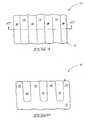
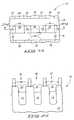
- FIGS. 45-48are views of the memory device 10 at a processing step subsequent to that of FIGS. 40-44 . More particularly, FIGS. 45 and 46 are top and cross-sectional views, respectively, of the memory device 10 and FIGS. 47 and 48 are top and cross-sectional views, respectively, of the memory device 10 rotated 90° from the embodiments illustrated in FIGS. 45 and 46 .
- an insulative material 56has been deposited atop the transistor gates 54 ( FIGS. 45 and 46 , for example).
- a conductivity dopantis implanted into the exposed surfaces of the silicon substrate 12 in order to form diffusion regions 59 , which may be transistor sources or drains ( FIGS. 47 and 48 , for example).
- the insulative material 56comprises spin-on-glass (SOG) and TEOS layers. Outermost portions of the insulative layer 56 may be removed by CMP or other planar etching methods to expose nitride runners 19 . Next, the nitride runners 19 are patterned and selectively etched to form opening 62 that extend through portions of the nitride runners 19 down to upper surface portions 58 of substrate 12 .
- a conductivity implantis performed to provide a conductivity dopant into upper surface portions 58 of runners 12 in order to form active areas 59 .
- the active areas 59comprise source/drain regions of devices such as, for example, transistors.
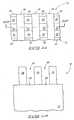
- FIGS. 49 and 50are views of the memory device 10 at a processing step subsequent to that of FIGS. 45-48 . More particularly, FIGS. 49 and 50 cross-sectional views, respectively, of the memory device 10 , where FIG. 49 is at the same orientation as FIG. 46 and FIG. 50 is at the same orientation as FIG. 48 .
- FIGS. 49 and 50illustrate transistors electrically coupled to charge storage devices. For example, exemplary transistor 69 is electrically coupled to exemplary capacitor 80 ( FIG. 50 ). The transistor 69 and capacitor 80 combine to form an exemplary memory cell 103 .
- a FET transistortypically comprises a gate, a gate dielectric, a source and drain, and a channel.
- the transistor 69comprises gate 54 , gate dielectric 52 , source/drain regions 41 and 59 , and channel 71 .
- FIG. 50illustrates arrows in the channel 71 which indicate current flow between the source/drain region 59 and the source/drain region 41 .
- activation of the transistor 69establishes a conductivity channel 71 from source/drain region 59 to source/drain region 41 .
- the source/drain region 59comprises a transistor source and the source/drain region 41 comprises a transistor drain.
- the source/drain region 59comprises a transistor drain and the source/drain region 41 comprises a transistor source.
- FIGS. 45-48Several process steps may be performed in order to transform the partially complete memory device 10 illustrated in FIGS. 45-48 to the memory device 100 illustrated in FIGS. 49 and 50 .
- Conductive materialsuch as polysilicon, for example, may then be deposited, forming an electrical contact 102 that couples with the capacitor 80 , for example.
- the transistor 69includes intermediate structures that insulate portions of the transistor 69 from the capacitor 80 .
- the transistor 69comprises a nitride cap 106 and insulative spacers 110 that are formed over the digit line 104 .
- a silicon dioxide layer 108may also be deposited on the nitride caps 106 .
- the capacitor 80comprises a capacitor dielectric 73 over a storage node 72 and a top cell plate 74 over the capacitor dielectric 73 .
- a dielectric plug 63is deposited above the transistor gates 54 and the active areas 59 .
- the dielectric plug 63comprises an oxide material, such as silicon dioxide, for example.
- the dielectric plug 63may then be patterned and etched to form contact holes that expose middle portions of the active areas 59 .
- Metal stackscomprising polysilicon and/or silicide layers, for example, may then be deposited in the contact holes in order to form digit lines 104 .
- the dielectric plug 63moves the digit line 104 conductor away from the silicon pillars 38 .
- the digit lines 104directly contact the active areas 59 so that a conductive plug is not necessary to electrically couple the digit lines 104 with the active areas 59 .
- Such conductive plugsare commonly formed in prior art transistors using epitaxial processes. By removing the need for an additional epitaxial process, the manufacturing defect rate may be decreased.
Landscapes
- Engineering & Computer Science (AREA)
- Manufacturing & Machinery (AREA)
- Semiconductor Memories (AREA)
Abstract
Description
- 1. Field of the Invention
- This invention relates to microelectronic devices and related fabrication methods. More particularly, this invention relates to a memory device having a digit line that is directly coupled to a transistor source.
- 2. Description of the Related Art
- Since the introduction of the digital computer, electronic storage devices have been a vital resource for the retention of data. Conventional semiconductor electronic storage devices, such as Dynamic Random Access Memory (DRAM), typically incorporate capacitor and transistor structures in which the capacitors temporarily store data based on the charged state of the capacitor structure. In general, this type of semiconductor Random Access Memory (RAM) often requires densely packed capacitor structures that are easily accessible for electrical interconnection.
- A DRAM cell typically comprises a charge storage capacitor (or cell capacitor) coupled to an access device, such as a Metal-Oxide-Semiconductor Field Effect Transistor (MOSFET, or simply FET). These access devices functions to apply or remove charge on the capacitor, thus affecting a logical state defined by the stored charge. The amount of charge stored on the capacitor is determined by the electrode (or storage node) area and the interelectrode spacing. The conditions of DRAM operation such as operating voltage, leakage rate and refresh rate, will generally mandate that a certain minimum charge be stored by the capacitor.
- FETs are widely used in integrated circuit devices including logic, memory and/or microprocessor devices that are used in consumer and/or industrial applications. As the integration density of integrated circuit FETs continues to increase, it may be desirable to continue to shrink the dimensions of the FETs. Conventionally, features of integrated circuit FETs may be formed on a microelectronic substrate, such as silicon semiconductor substrate, using photolithography and etching. As the minimum feature size is reduced, conventional fabrication techniques must also evolve in order to accurately fabricate the reduced size features. In some embodiments, fabrication of memory devices may be improved by reducing the number of processing steps involved in the fabrication process. In addition, improved transistor and charge storage devices may also decrease the manufacturing complexity, while maintaining or increasing the accuracy of the manufacturing process.
- In one embodiment, a memory device comprising a vertical transistor includes a digit line that is directly coupled to the source regions of each memory cell. In typical prior art memory devices, an electrical plug is deposited on an upper surface of the source regions and the digit line is electrically coupled to the electrical plug. By removing the electrical plug from the transistor design, processing steps are removed and the possibility for manufacturing defects is also reduced. Exemplary methods for fabricating a memory device having a source region configured to be directly coupled to a digit line are described below with respect to the figures.
- In another embodiment, a memory device comprising a vertical transistor includes gate regions that are recessed from an upper portion of a silicon substrate. With the gate regions recessed from the silicon substrate, the gate regions are spaced further from the source/drain regions and then in prior art vertical transistors and, accordingly, cross capacitance between the gate regions and the source/drain regions is reduced. By reducing cross capacitance between the gate region and the source/drain regions, the improved memory device design may increase accuracy of the memory device. Exemplary methods for fabricating a memory device having a recessed gate region are described below with respect to the figures.
- In one embodiment, a memory device comprises a semiconductor substrate having a first surface, a recessed gate formed in the substrate and defining a first and second lateral sides, a first source/drain region formed on the first surface of the semiconductor substrate adjacent the first lateral side of the recessed gate, a second source/drain region formed on the first surface of the semiconductor substrate adjacent the second lateral side of the recessed gate, wherein application of a voltage to the recessed gate results in formation of a conductive channel between the first and second source/drain regions along a path that is recessed into the semiconductor substrate, a charge storage device formed above the semiconductor substrate, wherein the charge storage device is electrically coupled to the first source/drain region, and a conductive data line interposed between the charge storage device and the first surface of the semiconductor substrate wherein the conductive data line comprises a first portion that extends at a first height above the first surface of the semiconductor substrate and a second portion that extends downward from the first portion to electrically contact the second source/drain region, and wherein the first and second portions are formed of the same material.
- In another embodiment, a method of fabricating a memory device comprises forming a semiconductor substrate having a first surface, forming a recessed gate in the substrate, wherein the recessed gate defines a first and second lateral sides, forming a first source/drain region on the first surface of the semiconductor substrate adjacent a first lateral side of the recessed gate, forming a second source/drain region on the first surface of the semiconductor substrate adjacent a second lateral side of the recessed gate, wherein application of a voltage to the gate results in the formation of a conductive channel between the first and second source/drain regions along a path that is recessed into the semiconductor substrate, forming a conductive data line between the charge storage device and the first surface of the semiconductor substrate, wherein the conductive data line comprises a first portion that extends a first height above the first surface of the semiconductor substrate and a second portion that extends downward from the first portion to electrically contact the second source/drain region, and wherein the first and second portions are formed of the same material, and forming a charge storage device above the semiconductor substrate, wherein the charge storage device is electrically coupled to the first source/drain region.
- In another embodiment, a memory device comprises a semiconductor substrate, a vertically extending gate region recessed in the substrate, a source region positioned on a first side of the gate, the source region being formed at least partially in the semiconductor substrate, a drain region positioned on a second side of the gate, wherein the second side is opposite the first side, and a digit line contact directly electrically connected to the source region and directly electrically connected to a digit line contact of the memory device.
- In another embodiment, a memory device comprises a source region, a drain region, a gate region separating the source and drain regions, and means for directly electrically coupling a digit line electrode of the memory device to the source region.
- In another embodiment, a memory array comprises a plurality of memory cells. In one embodiment, the array comprises a semiconductor substrate having a first surface, a plurality of recessed gates formed in the substrate, each defining respective first and second lateral sides, a plurality of first source/drain regions formed on the first surface of the semiconductor substrate adjacent respective first lateral sides of each recessed gate, a plurality of second source/drain regions formed on the first surface of the semiconductor substrate adjacent respective second lateral sides of each recessed gate, wherein application of a voltage to each gate results in the formation of a conductive channel between the respective first and second source/drain regions on either side of the gate along a path that is recessed into the semiconductor substrate, a plurality of charge storage devices formed above the semiconductor substrate, wherein the charge storage devices are electrically coupled to respective first source/drain regions, and a plurality of conductive data lines interposed between each the charge storage devices and the first surface of the semiconductor substrate. In one embodiment, the conductive data lines each comprise a first portion that extends at a first height above the first surface of the semiconductor substrate, and a second portion that extends downward from the first portion to electrically contact the second source/drain region.
- In another embodiment, a memory device comprises a semiconductor substrate having a first surface, a recessed gate that is formed in the substrate so as to be spaced a first distance from the first surface, wherein the recessed gate defines a first and second lateral sides, a first source/drain region formed on the first surface of the semiconductor substrate adjacent a first lateral side of the recessed gate, a second source/drain region formed on the first surface of the semiconductor substrate adjacent a second lateral side of the recessed gate wherein the application of voltage to the gate results in the formation of a conductive channel between the first and second source/drain regions along a path that is recessed into the semiconductor substrate and wherein the first distance is selected such that the gate structure is substantially located below the first and second source/drain regions so as to reduce the cross-capacitance between the gate and the first and second source/drain regions, a charge storage device formed above the semiconductor substrate wherein the charge storage device is electrically coupled to the first source/drain region, and a conductive data line interposed between the charge storage device and the first surface of the semiconductor substrate wherein the conductive data line electrically couples to the charge storage device when the gate is activated so as to transmit a signal indicative of the charge state of the charge storage device.
- In another embodiment, a memory device comprises a semiconductor substrate having a top surface, an active area positioned on a first side of the gate, the active area being formed in the semiconductor substrate, and a vertically extending gate positioned proximate the active area, wherein a top surface of the gate is elevationally below the top surface of the semiconductor substrate.
FIG. 1 is a top view of a portion of a memory device at an initial processing stage.FIG. 2 is a cross-sectional view taken a long line2-2 ofFIG. 1 .FIG. 3 is a top view of the memory device illustrated inFIG. 1 at a subsequent processing stage.FIG. 4 is a cross-sectional view of the memory device illustrated inFIG. 1 at a subsequent processing stage.FIG. 5 is a top view of thememory device 10 at a processing stage subsequent to that ofFIG. 3 .FIG. 6 is a cross-sectional view of thememory device 10 at a processing stage subsequent to that ofFIGS. 4 .FIG. 7 is a top view of thememory device 10 rotated 90° from the embodiment illustrated inFIG. 5 .FIG. 8 is a cross-sectional view of thememory device 10 rotated 90° from the embodiment illustrated inFIGS. 6 .FIG. 9 is a top view of thememory device 10 at a processing stage subsequent to that ofFIG. 5 .FIG. 10 is a cross-sectional view of thememory device 10 at a processing stage subsequent to that ofFIGS. 6 .FIG. 11 is a top view of thememory device 10 rotated 90° from the embodiment illustrated inFIG. 9 .FIG. 12 is a cross-sectional view of thememory device 10 rotated 90° from the embodiment illustrated inFIG. 10 .FIG. 13 is a top view of thememory device 10 at a processing stage subsequent to that ofFIG. 9 .FIG. 14 is a cross-sectional view of thememory device 10 at a processing stage subsequent to that ofFIG. 10 .FIG. 15 is a top view of thememory device 10 rotated 90° from the embodiment illustrated inFIG. 13 .FIG. 16 is a cross-sectional view of thememory device 10 rotated 90° from the embodiment illustrated inFIG. 14 .FIG. 17 is a top view of thememory device 10 at a processing stage subsequent to that ofFIG. 13 .FIG. 18 is a cross-sectional view of thememory device 10 at a processing stage subsequent to that ofFIG. 14 .FIG. 19 is a top view of thememory device 10 rotated 90° from the embodiment illustrated inFIG. 17 .FIG. 20 is a cross-sectional view of thememory device 10 rotated 90° from the embodiment illustrated inFIG. 18 .FIG. 21 is a top view of thememory device 10 at a processing stage subsequent to that ofFIG. 17 .FIG. 22 is a cross-sectional view of thememory device 10 at a processing stage subsequent to that ofFIG. 18 .FIG. 23 is a top view of thememory device 10 rotated 90° from the embodiment illustrated inFIG. 21 .FIG. 24 is a cross-sectional view of thememory device 10 rotated 90° from the embodiment illustrated inFIG. 22 .FIG. 25 is a top view of thememory device 10 at a processing stage subsequent to that ofFIG. 21 .FIG. 26 is a cross-sectional view of thememory device 10 at a processing stage subsequent to that ofFIG. 22 .FIG. 27 is a top view of thememory device 10 rotated 90° from the embodiment illustrated inFIG. 25 .FIG. 28 is a cross-sectional view of thememory device 10 rotated 90° from the embodiment illustrated inFIG. 26 .FIG. 29 is a top view of thememory device 10 at a processing stage subsequent to that ofFIG. 25 .FIG. 30 is a cross-sectional view of thememory device 10 at a processing stage subsequent to that ofFIG. 26 .FIG. 31 is a top view of thememory device 10 rotated 90° from the embodiment illustrated inFIG. 29 .FIG. 32 is a cross-sectional view of thememory device 10 rotated 90° from the embodiment illustrated inFIG. 30 .FIG. 33 is a top view of thememory device 10 at a processing stage subsequent to that ofFIG. 29 .FIG. 34 is a cross-sectional view of thememory device 10 at a processing stage subsequent to that ofFIG. 30 .FIG. 35 is a top view of thememory device 10 rotated 90° from the embodiment illustrated inFIG. 33 .FIG. 36 is a cross-sectional view of thememory device 10 rotated 90° from the embodiment illustrated inFIG. 34 .FIG. 37 is a top view of thememory device 10 at a processing stage subsequent to that ofFIG. 33 .FIG. 38 is a cross-sectional view of thememory device 10 at a processing stage subsequent to that ofFIG. 34 .FIG. 39 is a top view of thememory device 10 rotated 90° from the embodiment illustrated inFIG. 37 .FIG. 40 is a cross-sectional view of thememory device 10 rotated 90° from the embodiment illustrated inFIG. 38 .FIG. 41 is a top view of thememory device 10 at a processing stage subsequent to that ofFIG. 37 .FIG. 42 is a cross-sectional view of thememory device 10 at a processing stage subsequent to that ofFIG. 38 .FIG. 43 is a top view of thememory device 10 rotated 90° from the embodiment illustrated inFIG. 41 .FIG. 44 is a cross-sectional view of thememory device 10 rotated 90° from the embodiment illustrated inFIG. 42 .FIG. 45 is a top view of thememory device 10 at a processing stage subsequent to that ofFIGS. 41 .FIG. 46 is a cross-sectional view of thememory device 10 at a processing stage subsequent to that ofFIG. 42 .FIG. 47 is a top view of thememory device 10 rotated 90° from the embodiment illustrated inFIG. 45 .FIG. 48 is a cross-sectional view of thememory device 10 rotated 90° from the embodiment illustrated inFIG. 46 .FIG. 49 is a cross-sectional view of the memory device10 (at the same orientation asFIG. 46 ) at a subsequent processing stage.FIG. 50 is a cross-sectional view of the memory device10 (at the same orientation asFIG. 48 ) at a subsequent processing stage.- Embodiments of the invention will now be described with reference to the accompanying figures, wherein like numerals refer to like elements throughout. The terminology used in the description presented herein is not intended to be interpreted in any limited or restrictive manner, simply because it is being utilized in conjunction with a detailed description of certain specific embodiments of the invention. Furthermore, embodiments of the invention may include several novel features, no single one of which is solely responsible for its desirable attributes or which is essential to practicing the inventions herein described.
FIGS. 1 and 2 illustrate asemiconductor substrate 12 having shallow trench isolation (STI)regions 14. More particularly,FIG. 1 is a top view of a portion of amemory device 10 at an initial processing stage, wherein thememory device 10 includes thesubstrate 12 patterned withSTI regions 14 andpillars 16. As illustrated inFIG. 1 , theSTI regions 14 andpillars 16 alternate in thesubstrate 12.FIG. 2 is a cross-sectional view taken a long line2-2 ofFIG. 1 . As illustrated inFIG. 2 , theSTI regions 14form pillars 16 in thesubstrate 12.FIGS. 3 and 4 are top and cross-sectional views, respectively, of thememory device 10 at processing stage subsequent to the embodiment illustrated inFIGS. 1 and 2 . As illustrated inFIGS. 3 and 4 , anitride layer 18 has been deposited on the upper services of thepillars 16 andSTI regions 14. The dashed lines inFIG. 3 indicate surfaces that are not visible from the top view. Thus, thepillars 16 andSTI regions 14 are not visible from the top view illustrated inFIG. 3 , due to the deposition ofnitride layer 18 on top of these surfaces. In one embodiment, thenitride layer 18 has a thickness in the range of about 2000 to 3000 Angstroms. In other embodiments, however, the thickness of thenitride layer 18 may be adjusted according to various design parameters.FIGS. 5-8 are views of thememory device 10 at a processing stage subsequent to that ofFIGS. 3 and 4 . More particularly,FIGS. 5 and 6 are top and cross-sectional views, respectively, andFIGS. 7 and 8 are top and cross-sectional views, respectively, rotated 90° from the embodiments illustrated inFIGS. 5 and 6 . As illustrated inFIG. 8 , for example, thenitride layer 18 has been patterned and etched to formtrenches 20 in thenitride layer 18. In the embodiment ofFIG. 8 , thetrenches 20 extend to anupper surface 22 of thesubstrate 12. Thetrenches 20 also exposeisolation region portions 24 of theSTI regions 14. As illustrated inFIG. 5-8 , thenitride layer 18 is now patterned so thatnitride runners 19 extend vertically from thesubstrate 12 and are generally separated by thetrenches 20 and are parallel to one another. As illustrated inFIG. 7 , for example, theupper surface portions 22 of thesubstrate 12 are generally surrounded by theisolation region portions 24 and thenitride layer 18. In one embodiment, theupper surface portions 22 are generally shaped as squares.FIGS. 9-12 are views of thememory device 10 at a processing step subsequent to that ofFIGS. 5-8 . More particularly,FIGS. 9 and 10 are top and cross-sectional views, respectively, of thememory device 10 andFIGS. 11 and 12 are top and cross-sectional views, respectively, of thememory device 10 rotated 90° from the embodiments illustrated inFIGS. 9 and 10 . As illustrated inFIG. 10 , for example, isolation region portions24 (FIG. 6 ) are etched below theupper surface portions 22 ofsubstrate 12 in order to expose recessedsurfaces 26 of theSTI regions 14. In one embodiment, theisolation region portions 24 are etched using a reactive ion etch (RIE) process to selectively etch thenitride runners 19. As shown inFIG. 10 , the etch process exposes sidewalls27 of thesubstrate 12 which were originally covered by an insulative material deposited in theSTI regions 14. In one embodiment, the recessed surfaces26 are in the range of about 500 to 1500 Angstroms below theupper surface portions 22 of thesubstrate 12. In another embodiment, the recessed surfaces26 are in the range of about 800 to 1200 Angstroms below theupper surface portions 22 of thesubstrate 12. In other embodiments, the recessed surfaces26 may extend other distances below theupper surface portions 22.- In one embodiment, after the recessed surfaces26 are exposed using an etching process, for example, residual oxide on the
sidewalls 27 andupper surface portions 22 is removed. In one embodiment, a wet hydrofluoric (HF) etch is used to remove these residual oxides. In other embodiments, other clean etches may be used in order to achieve similar results. FIGS. 13-16 are views of thememory device 10 at a processing step subsequent to that ofFIGS. 9-12 . More particularly,FIGS. 13 and 14 are top and cross-sectional views, respectively, of thememory device 10 andFIGS. 15 and 16 are top and cross-sectional views, respectively, of thememory device 10 rotated 90° from the embodiments illustrated inFIGS. 13 and 14 . As illustrated inFIGS. 14 and 16 , for example, anitride liner 28 has been deposited on theupper surface 22 of thesubstrate 12, the recessed surfaces26, and thesidewalls 27. In one embodiment, thenitride liner 28 has a thickness in the range of about 30 to 100 Angstroms.- After depositing the
nitride liner 28, asacrificial layer 30, such as a spin-on-glass (SOG), for example, is deposited in the trenches20 (FIG. 12 ) between thenitride runners 19. In other embodiments, the sacrificial layer may comprise other materials, such as borophosphorous silica glass (BPSG) and/or TEOS. In one embodiment, thesacrificial layer 30 is etched so that thesacrificial layer 30 is planar with thenitride runners 19. In one embodiment, thesacrificial layer 30 is removed using a chemical mechanical polishing (CMP) process; however other etching processes may be used in order to adjust a height of thesacrificial layer 30. FIGS. 17-20 are views of thememory device 10 at a processing step subsequent to that ofFIGS. 13-16 . More particularly,FIGS. 17 and 18 are top and cross-sectional views, respectively, of thememory device 10 andFIGS. 19 and 20 are top and cross-sectional views, respectively, of thememory device 10 rotated 90° from the embodiments illustrated inFIGS. 17 and 18 . As illustrated inFIG. 18 , for example, a portion of thesacrificial layer 30 is selectively etched in order to expose thenitride liner 28 overupper surface portions 22 ofsubstrate 12. Thesacrificial layer 30 is selectively etched so that columns remain extending upward above theSTI regions 14. As shown inFIG. 18 , the exposed portions of thenitride liner 28 on theupper surface portions 22 are removed to expose theupper surface portions 22 of thesilicon substrate 12 between the pillars of thesacrificial layer 30. In one embodiment, a selective nitride etch is used to etch thenitride liner 28 from theupper surface portions 22 of thesubstrate 12. After removing portions of thesacrificial layer 30 and thenitride liner 28 as described above,openings 31 extend to expose theupper surface portions 22. In one embodiment, the exposedupper surface portions 22 function as active areas for thememory device 10.FIGS. 21-24 are views of thememory device 10 at a processing step subsequent to that ofFIGS. 17-20 . More particularly,FIGS. 21 and 22 are top and cross-sectional views, respectively, of thememory device 10 andFIGS. 23 and 24 are top and cross-sectional views, respectively, of thememory device 10 rotated 90° from the embodiments illustrated inFIGS. 21 and 22 . As illustrated inFIGS. 21-24 ,insulative spacers 34 have been formed on either side of the sacrificial layer30 (e.g.,FIG. 22 ) and the nitride runners19 (e.g.,FIG. 24 ). In one embodiment, theinsulative spacers 34 comprise Tetraethyl Orthosilicate (TEOS).- In one embodiment, a layer of insulative material is deposited over the
silicon substrate 12 in order to fill the openings31 (FIG. 18 ). The insulative material is then anisotropically etched to form thesacrificial insulative spacers 34. For example, in one embodiment, a reactive ion etch is used to remove portions of the insulative material, leaving only about 200 to 500 Angstroms of material surrounding thenitride runners 19 and thesacrificial layer 30. As illustrated inFIGS. 21 and 23 , for example, the etching of the insulative material leaves a generallycylindrical openings 32 that expose a smaller surface area of theupper surface portion 22. In one embodiment, theinsulative spacers 34 improve the critical dimensions possible for subsequently formed structures that are formed over or uponupper surface portions 22 of thesilicon substrate 12. FIGS. 25-28 are views of thememory device 10 at a processing step subsequent to that ofFIGS. 21-24 . More particularly,FIGS. 25 and 26 are top and cross-sectional views, respectively, of thememory device 10 andFIGS. 27 and 28 are top and cross-sectional views, respectively, of thememory device 10 rotated 90° from the embodiments illustrated inFIGS. 25 and 26 . As illustrated inFIG. 26 , for example, an additional nitride material is deposited inside thespacers 34 forming nitride plugs33 that fill the openings32 (FIG. 22 ). The nitride plugs33 may be formed by depositing a nitride material in thecylindrical openings 32 and then selectively etching the nitride material to form the nitride plugs33 inside thesacrificial insulative spacers 34. In one embodiment, the nitride plugs33 have a thickness in the range of about500 to1200 Angstroms between thespacers 34.FIGS. 29-32 are views of thememory device 10 at a processing step subsequent to that ofFIGS. 25-28 . More particularly,FIGS. 29 and 30 are top and cross-sectional views, respectively, of thememory device 10 andFIGS. 31 and 32 are top and cross-sectional views, respectively, of thememory device 10 rotated 90° from the embodiments illustrated inFIGS. 29 and 30 .- In the embodiment of
FIGS. 29-32 , nitride plugs38 extend upward from the exposedupper surface portions 22 of thesilicon substrate 12 in thecylindrical openings 32. In one embodiment, upper surfaces of the nitride plugs33 (FIG. 28 ),nitride layer 18, andinsulative spacers 34 are removed using a blanket nitride etch or CMP in order to form the nitride plugs38. In one embodiment, the nitride plugs38 are elevationally level with, or below,upper surfaces 47 of thenitride runners 19. FIGS. 33-36 are views of thememory device 10 at a processing step subsequent to that ofFIGS. 29-32 . More particularly,FIGS. 33 and 34 are top and cross-sectional views, respectively, of thememory device 10 andFIGS. 35 and 36 are top and cross-sectional views, respectively, of thememory device 10 rotated 90° from the embodiments illustrated inFIGS. 33 and 34 . As illustrated inFIGS. 34 and 36 , for example, thesacrificial layers 30 and the insulative spacers34 (shown inFIG. 30 , for example) have been removed. In one embodiment, thesacrificial layer 30 andinsulative spacers 34 are entirely removed using an etching process, such as a diluted hydrofluoric acid etch and/or a buffered oxide etch. In other embodiments, other materials may be used to selectively etch thesacrificial layer 30 and theinsulative spacers 34. In an advantageous embodiment, the selective etch stops etching at nitride and silicon materials, such as thenitride liner 28,nitride runners 19, andupper surface portions 22 ofsilicon substrate 12. As shown inFIG. 34 , the selectiveetching forms openings 42 that are defined bynitride liner 28 andnitride runners 19.FIGS. 37-40 are views of thememory device 10 at a processing step subsequent to that ofFIGS. 33-36 . More particularly,FIGS. 37 and 38 are top and cross-sectional views, respectively, of thememory device 10 andFIGS. 39 and 40 are top and cross-sectional views, respectively, of thememory device 10 rotated 90° from the embodiments illustrated inFIGS. 37 and 38 . At the processing stage illustrated inFIGS. 37-40 , at least a portion of thenitride liner 28, theupper surface portions 22 ofsubstrate 12, and theSTI region 14 are removed using-one or more etching processes. In one embodiment, portions of the nitride plugs38 is also etched when thenitride liner 28, andsubstrate 12, andSTI region 14 are etched as described above. Accordingly, in this embodiment, the height of the nitride plugs38 is decreased due to this etching. After this etching is complete, aninsulative film 52 is deposited on the exposed surfaces of thesilicon substrate 12. After completion of these processing steps, which are discussed in further detail below, achannel 21 is created in thesilicon substrate 12, wherein a length of the channel is determined by the depth of the etching.- In one embodiment, a dry/wet nitride punch etch, using, for example, H3PO4solution, is used to remove the nitride liner28 (
FIG. 30 ) from over theSTI region 14, thesilicon substrate 12 and theupper surface portions 22. - In one embodiment, a selective dry etch is used to remove portions of the
upper surface portions 12 adjacent the nitride plugs38. The selective dry etch may also removed portions of theSTI region 14, while leaving portions of thesilicon substrate 12 directly below the nitride plugs38. The portions of thesilicon substrate 12 that remain below the nitride plugs38 are hereinafter referred to assilicon support structures 46. In one embodiment, thesupport structures 46 are generally annular or cylindrical shaped, similar to the nitride plugs38 which extend above thesilicon support structures 46, As illustrated inFIG. 38 , for example, the selective etching enlarges openings42 (FIG. 34 ) to formenlarged openings 44. Theenlarged openings 44 are defined by thesilicon support structures 46, anupper surface 48 of thesilicon substrate 12, and anupper surface 50 of theSTI regions 14. In one embodiment, the etching process will remove slightly more of thesilicon substrate 12 than theSTI region 14. In this embodiment, theupper surface 48 of thesilicon substrate 12 is slightly below theupper surface 50 of theSTI regions 14. - After forming the
enlarged openings 44, aninsulative film 52 is grown over the exposed portions of thesilicon substrate 12 and thesilicon support structures 46. In one embodiment, theinsulative film 52 comprises an oxide, such as silicon dioxide. Referring toFIG. 38 , for example, theinsulative film 52 can be seen covering the side walls of the nitride plugs38 and thesilicon support structures 46, as well as theupper surface 48 of thesilicon substrate 12. In some embodiments, the insulative film serves as a gate oxide dielectric for transistors. An exemplary method of forming the dielectric may include CVD deposition of a low K material on the exposed silicon surfaces of theupper surface 48 of thesilicon substrate 12, thesilicon support structures 46, and the side walls of the nitride plugs38. - In one embodiment, the
silicon support structures 46 serve as a portion of a channel for transistors of thememory device 10. Accordingly, the length of thesilicon support structures 46 defines a vertical length of thetransistor channel 21. In the embodiments illustrated inFIGS. 37-40 , because thetransistor channel 21 extends perpendicularly to the orientation ofsubstrate 12, thetransistor channel 21 defines a channel of a vertical transistor. FIGS. 41-44 are views of thememory device 10 at a processing step subsequent to that ofFIGS. 37-40 . More particularly,FIGS. 41 and 42 are top and cross-sectional views, respectively, of thememory device 10 andFIGS. 43 and 44 are top and cross-sectional views, respectively, of thememory device 10 rotated 90° from the embodiments illustrated inFIGS. 41 and 42 . At the stage of processing illustrated inFIGS. 41-44 ,diffusion regions 41 have been formed below the nitride plugs38 andtransistor gates 54 have been formed over theinsulative film 52. In one embodiment, thetransistor gates 54 comprise word lines of thememory device 10, such as a DRAM.- In one embodiment, an implant method may be used to transfer a conductivity dopant through the nitride plugs38 to the
silicon substrate 12 directly beneath the nitride plugs38. In another embodiment, an angle implant method may be used to form thediffusion regions 41. For example, Arsenic or Phosphorous may be implanted in thesubstrate 12, below the nitride plugs38, angled from within the openings44 (FIG. 38 ). Those of skill in the art will recognize that various alternative methods and doping materials may be used in forming thediffusions regions 41. Any suitable doping method may be used to create thediffusion regions 41. In one embodiment, thediffusion regions 41 are configured to serve as source/drain regions of a transistor device. More generally, thediffusion regions 41 may be used as electrical contacts between charge storage devices, such as capacitors, and other components of a transistor and/or a memory device. - In one embodiment, a conductive material, such as polysilicon, is deposited on the
insulative film 52 and theSTI region 14. In some embodiments, portions of the deposited conductive material may be removed by a polishing process, such as CMP, to an elevation below thesilicon pillars 38. For example,FIG. 42 illustrates theupper surfaces 55 of thetransistor gate 54 about 1000 Angstroms below theupper surfaces 39 of thesilicon pillars 38. - In an advantageous embodiment, the
transistor gates 54 are recessed from the silicon substrate so that the gate regions are spaced further from the source/drain regions of the transistor devices in thememory 10. In the embodiment ofFIG. 42 , for example, thetransistor gates 54 are recessed below an upper surface of thesubstrate 12. In other embodiments, thetransistor gates 54 are recessed about 500 Angstroms, or in the range of about 250 to 1,000 Angstroms, below an upper surface of thesubstrate 12. Accordingly, cross capacitance between the gate regions and the source/drain regions may be reduced, thus improving the accuracy of the memory device. FIGS. 45-48 are views of thememory device 10 at a processing step subsequent to that ofFIGS. 40-44 . More particularly,FIGS. 45 and 46 are top and cross-sectional views, respectively, of thememory device 10 andFIGS. 47 and 48 are top and cross-sectional views, respectively, of thememory device 10 rotated 90° from the embodiments illustrated inFIGS. 45 and 46 . At the processing stage illustrated inFIGS. 45-48 , aninsulative material 56 has been deposited atop the transistor gates54 (FIGS. 45 and 46 , for example). In addition, a conductivity dopant is implanted into the exposed surfaces of thesilicon substrate 12 in order to formdiffusion regions 59, which may be transistor sources or drains (FIGS. 47 and 48 , for example).- In one embodiment, the
insulative material 56 comprises spin-on-glass (SOG) and TEOS layers. Outermost portions of theinsulative layer 56 may be removed by CMP or other planar etching methods to exposenitride runners 19. Next, thenitride runners 19 are patterned and selectively etched to form opening62 that extend through portions of thenitride runners 19 down toupper surface portions 58 ofsubstrate 12. - As illustrated in
FIG. 48 , for example, a conductivity implant is performed to provide a conductivity dopant intoupper surface portions 58 ofrunners 12 in order to formactive areas 59. In one embodiment, theactive areas 59 comprise source/drain regions of devices such as, for example, transistors. FIGS. 49 and 50 are views of thememory device 10 at a processing step subsequent to that ofFIGS. 45-48 . More particularly,FIGS. 49 and 50 cross-sectional views, respectively, of thememory device 10, whereFIG. 49 is at the same orientation asFIG. 46 andFIG. 50 is at the same orientation asFIG. 48 .FIGS. 49 and 50 illustrate transistors electrically coupled to charge storage devices. For example,exemplary transistor 69 is electrically coupled to exemplary capacitor80 (FIG. 50 ). Thetransistor 69 andcapacitor 80 combine to form anexemplary memory cell 103.- Those of skill in the art will recognize that a FET transistor typically comprises a gate, a gate dielectric, a source and drain, and a channel. In the embodiment of
FIGS. 49 and 50 , thetransistor 69 comprisesgate 54,gate dielectric 52, source/drain regions FIG. 50 illustrates arrows in the channel71 which indicate current flow between the source/drain region 59 and the source/drain region 41. Thus, in one embodiment, activation of thetransistor 69 establishes a conductivity channel71 from source/drain region 59 to source/drain region 41. In one embodiment, the source/drain region 59 comprises a transistor source and the source/drain region 41 comprises a transistor drain. In one embodiment, the source/drain region 59 comprises a transistor drain and the source/drain region 41 comprises a transistor source. - Several process steps may be performed in order to transform the partially
complete memory device 10 illustrated inFIGS. 45-48 to thememory device 100 illustrated inFIGS. 49 and 50 . Initially, at least portions of theinsulative material 56, thesilicon support structures 46, and the nitride plugs38 are removed in order to expose the source/drain regions 41. Conductive material, such as polysilicon, for example, may then be deposited, forming anelectrical contact 102 that couples with thecapacitor 80, for example. In the embodiment ofFIGS. 49 and 50 , thetransistor 69 includes intermediate structures that insulate portions of thetransistor 69 from thecapacitor 80. For example, thetransistor 69 comprises anitride cap 106 andinsulative spacers 110 that are formed over thedigit line 104. In one embodiment, asilicon dioxide layer 108 may also be deposited on the nitride caps106. In one embodiment, thecapacitor 80 comprises acapacitor dielectric 73 over astorage node 72 and atop cell plate 74 over thecapacitor dielectric 73. - In the embodiment of
FIGS. 49 and 50 , adielectric plug 63 is deposited above thetransistor gates 54 and theactive areas 59. In one embodiment, thedielectric plug 63 comprises an oxide material, such as silicon dioxide, for example. Thedielectric plug 63 may then be patterned and etched to form contact holes that expose middle portions of theactive areas 59. Metal stacks comprising polysilicon and/or silicide layers, for example, may then be deposited in the contact holes in order to form digit lines104. Thus, thedielectric plug 63 moves thedigit line 104 conductor away from thesilicon pillars 38. Advantageously, thedigit lines 104 directly contact theactive areas 59 so that a conductive plug is not necessary to electrically couple thedigit lines 104 with theactive areas 59. Such conductive plugs are commonly formed in prior art transistors using epitaxial processes. By removing the need for an additional epitaxial process, the manufacturing defect rate may be decreased. - The foregoing description details certain embodiments of the invention. It will be appreciated, however, that no matter how detailed the foregoing appears in text, the invention can be practiced in many ways. As is also stated above, it should be noted that the use of particular terminology when describing certain features or aspects of the invention should not be taken to imply that the terminology is being re-defined herein to be restricted to including any specific characteristics of the features or aspects of the invention with which that terminology is associated. The scope of the invention should therefore be construed in accordance with the appended claims and any equivalents thereof.
Claims (23)
Priority Applications (4)
| Application Number | Priority Date | Filing Date | Title |
|---|---|---|---|
| US11/218,184US7696567B2 (en) | 2005-08-31 | 2005-08-31 | Semiconductor memory device |
| US12/703,502US8222105B2 (en) | 2005-08-31 | 2010-02-10 | Methods of fabricating a memory device |
| US13/469,513US8481385B2 (en) | 2005-08-31 | 2012-05-11 | Methods of fabricating a memory device |
| US13/781,862US8546215B2 (en) | 2005-08-31 | 2013-03-01 | Methods of fabricating a memory device |
Applications Claiming Priority (1)
| Application Number | Priority Date | Filing Date | Title |
|---|---|---|---|
| US11/218,184US7696567B2 (en) | 2005-08-31 | 2005-08-31 | Semiconductor memory device |
Related Child Applications (1)
| Application Number | Title | Priority Date | Filing Date |
|---|---|---|---|
| US12/703,502ContinuationUS8222105B2 (en) | 2005-08-31 | 2010-02-10 | Methods of fabricating a memory device |
Publications (2)
| Publication Number | Publication Date |
|---|---|
| US20070051997A1true US20070051997A1 (en) | 2007-03-08 |
| US7696567B2 US7696567B2 (en) | 2010-04-13 |
Family
ID=37829252
Family Applications (4)
| Application Number | Title | Priority Date | Filing Date |
|---|---|---|---|
| US11/218,184Active2027-01-26US7696567B2 (en) | 2005-08-31 | 2005-08-31 | Semiconductor memory device |
| US12/703,502Expired - LifetimeUS8222105B2 (en) | 2005-08-31 | 2010-02-10 | Methods of fabricating a memory device |
| US13/469,513Expired - LifetimeUS8481385B2 (en) | 2005-08-31 | 2012-05-11 | Methods of fabricating a memory device |
| US13/781,862Expired - LifetimeUS8546215B2 (en) | 2005-08-31 | 2013-03-01 | Methods of fabricating a memory device |
Family Applications After (3)
| Application Number | Title | Priority Date | Filing Date |
|---|---|---|---|
| US12/703,502Expired - LifetimeUS8222105B2 (en) | 2005-08-31 | 2010-02-10 | Methods of fabricating a memory device |
| US13/469,513Expired - LifetimeUS8481385B2 (en) | 2005-08-31 | 2012-05-11 | Methods of fabricating a memory device |
| US13/781,862Expired - LifetimeUS8546215B2 (en) | 2005-08-31 | 2013-03-01 | Methods of fabricating a memory device |
Country Status (1)
| Country | Link |
|---|---|
| US (4) | US7696567B2 (en) |
Cited By (14)
| Publication number | Priority date | Publication date | Assignee | Title |
|---|---|---|---|---|
| US20080012070A1 (en)* | 2005-07-08 | 2008-01-17 | Werner Juengling | Apparatus for a self-aligned recessed access device (rad) transistor gate |
| US20080142882A1 (en)* | 2004-09-01 | 2008-06-19 | Tang Sanh D | Transistors |
| US20090311845A1 (en)* | 2006-09-07 | 2009-12-17 | Micron Technology, Inc. | One Transistor Memory Cell with Bias Gate |
| US7700441B2 (en) | 2006-02-02 | 2010-04-20 | Micron Technology, Inc. | Methods of forming field effect transistors, methods of forming field effect transistor gates, methods of forming integrated circuitry comprising a transistor gate array and circuitry peripheral to the gate array, and methods of forming integrated circuitry comprising a transistor gate array including first gates and second grounded isolation gates |
| US20100273303A1 (en)* | 2006-08-21 | 2010-10-28 | Micron Technology, Inc. | Memory Arrays and Methods of Fabricating Memory Arrays |
| US7867851B2 (en) | 2005-08-30 | 2011-01-11 | Micron Technology, Inc. | Methods of forming field effect transistors on substrates |
| US7897460B2 (en) | 2005-03-25 | 2011-03-01 | Micron Technology, Inc. | Methods of forming recessed access devices associated with semiconductor constructions |
| US20120001255A1 (en)* | 2010-07-01 | 2012-01-05 | Hynix Semiconductor Inc. | Semiconductor device and method for forming the same |
| US8551823B2 (en) | 2006-07-17 | 2013-10-08 | Micron Technology, Inc. | Methods of forming lines of capacitorless one transistor DRAM cells, methods of patterning substrates, and methods of forming two conductive lines |
| US20150236023A1 (en)* | 2011-08-23 | 2015-08-20 | Micron Technology, Inc. | Vertical Transistor Devices, Memory Arrays, And Methods Of Forming Vertical Transistor Devices |
| US10515801B2 (en) | 2007-06-04 | 2019-12-24 | Micron Technology, Inc. | Pitch multiplication using self-assembling materials |
| WO2022115229A1 (en)* | 2020-11-30 | 2022-06-02 | Micron Technology, Inc. | An array of capacitors, an array of memory cells, method used in forming an array of memory cells, methods used in forming an array of capacitors, and methods used in forming a plurality of horizontally- spaced conductive lines |
| US11557593B2 (en) | 2020-11-30 | 2023-01-17 | Micron Technology, Inc. | Array of memory cells, methods used in forming an array of memory cells, methods used in forming an array of vertical transistors, and methods used in forming an array of capacitors |
| US11744061B2 (en) | 2019-08-26 | 2023-08-29 | Micron Technology, Inc. | Array of capacitors, an array of memory cells, a method of forming an array of capacitors, and a method of forming an array of memory cells |
Families Citing this family (13)
| Publication number | Priority date | Publication date | Assignee | Title |
|---|---|---|---|---|
| US7858471B2 (en) | 2006-09-13 | 2010-12-28 | Micron Technology, Inc. | Methods of fabricating an access transistor for an integrated circuit device, methods of fabricating periphery transistors and access transistors, and methods of fabricating an access device comprising access transistors in an access circuitry region and peripheral transistors in a peripheral circuitry region spaced from the access circuitry region |
| KR101432619B1 (en)* | 2008-07-07 | 2014-08-21 | 삼성전자주식회사 | Semiconductor device and manufacturing method thereof |
| US8692310B2 (en) | 2009-02-09 | 2014-04-08 | Spansion Llc | Gate fringing effect based channel formation for semiconductor device |
| JP2010219326A (en)* | 2009-03-17 | 2010-09-30 | Elpida Memory Inc | Semiconductor memory device and method of manufacturing the same |
| US8750040B2 (en) | 2011-01-21 | 2014-06-10 | Micron Technology, Inc. | Memory devices having source lines directly coupled to body regions and methods |
| US8907396B2 (en) | 2012-01-04 | 2014-12-09 | Micron Technology, Inc | Source/drain zones with a delectric plug over an isolation region between active regions and methods |
| US9064745B2 (en) | 2012-08-29 | 2015-06-23 | International Business Machines Corporation | Sublithographic width finFET employing solid phase epitaxy |
| KR102001417B1 (en) | 2012-10-23 | 2019-07-19 | 삼성전자주식회사 | Semiconductor device |
| US9570447B2 (en)* | 2013-01-23 | 2017-02-14 | Longitude Semiconductor S.A.R.L. | Semiconductor device and production method therefor |
| KR102707534B1 (en) | 2016-12-02 | 2024-09-20 | 삼성전자주식회사 | Semiconductor memory device |
| US10446606B2 (en) | 2017-07-19 | 2019-10-15 | International Business Machines Corporation | Back-side memory element with local memory select transistor |
| US10818800B2 (en) | 2017-12-22 | 2020-10-27 | Nanya Technology Corporation | Semiconductor structure and method for preparing the same |
| US11049864B2 (en)* | 2019-05-17 | 2021-06-29 | Micron Technology, Inc. | Apparatuses including capacitor structures, and related memory devices, electronic systems, and methods |
Citations (97)
| Publication number | Priority date | Publication date | Assignee | Title |
|---|---|---|---|---|
| US3941629A (en)* | 1974-04-11 | 1976-03-02 | General Motors Corporation | Diaphragm formation on silicon substrate |
| US4139442A (en)* | 1977-09-13 | 1979-02-13 | International Business Machines Corporation | Reactive ion etching method for producing deep dielectric isolation in silicon |
| US4432132A (en)* | 1981-12-07 | 1984-02-21 | Bell Telephone Laboratories, Incorporated | Formation of sidewall oxide layers by reactive oxygen ion etching to define submicron features |
| US4502914A (en)* | 1982-11-13 | 1985-03-05 | International Business Machines Corporation | Method of making structures with dimensions in the sub-micrometer range |
| US4570325A (en)* | 1983-12-16 | 1986-02-18 | Kabushiki Kaisha Toshiba | Manufacturing a field oxide region for a semiconductor device |
| US4648937A (en)* | 1985-10-30 | 1987-03-10 | International Business Machines Corporation | Method of preventing asymmetric etching of lines in sub-micrometer range sidewall images transfer |
| US4903344A (en)* | 1987-07-07 | 1990-02-20 | Oki Electric Industry Co., Ltd. | Semiconductor memory device with staggered sense amplifiers |
| US4983544A (en)* | 1986-10-20 | 1991-01-08 | International Business Machines Corporation | Silicide bridge contact process |
| US5087586A (en)* | 1991-07-03 | 1992-02-11 | Micron Technology, Inc. | Process for creating fully-recessed field isolation regions by oxidizing a selectively-grown epitaxial silicon layer |
| US5195092A (en)* | 1987-08-04 | 1993-03-16 | Telaction Corporation | Interactive multimedia presentation & communication system |
| US5497017A (en)* | 1995-01-26 | 1996-03-05 | Micron Technology, Inc. | Dynamic random access memory array having a cross-point layout, tungsten digit lines buried in the substrate, and vertical access transistors |
| US5502320A (en)* | 1993-03-15 | 1996-03-26 | Kabushiki Kaisha Toshiba | Dynamic random access memory (DRAM) semiconductor device |
| US5596759A (en)* | 1989-11-03 | 1997-01-21 | Compaq Computer Corporation | Method for initializing a multiple processor computer system using a common ROM |
| US5604159A (en)* | 1994-01-31 | 1997-02-18 | Motorola, Inc. | Method of making a contact structure |
| US5607874A (en)* | 1996-02-02 | 1997-03-04 | Taiwan Semiconductor Manufacturing Company, Ltd. | Method for fabricating a DRAM cell with a T shaped storage capacitor |
| US5705321A (en)* | 1993-09-30 | 1998-01-06 | The University Of New Mexico | Method for manufacture of quantum sized periodic structures in Si materials |
| US5861328A (en)* | 1996-10-07 | 1999-01-19 | Motorola, Inc. | Method of fabricating GMR devices |
| US5864496A (en)* | 1997-09-29 | 1999-01-26 | Siemens Aktiengesellschaft | High density semiconductor memory having diagonal bit lines and dual word lines |
| US6010946A (en)* | 1996-08-21 | 2000-01-04 | Nec Corporation | Semiconductor device with isolation insulating film tapered and method of manufacturing the same |
| US6014633A (en)* | 1997-09-24 | 2000-01-11 | Deroyal Business Systems, L.L.C. | Method for the analysis and standardization of bills of resources |
| US6042998A (en)* | 1993-09-30 | 2000-03-28 | The University Of New Mexico | Method and apparatus for extending spatial frequencies in photolithography images |
| US6172391B1 (en)* | 1997-08-27 | 2001-01-09 | Siemens Aktiengesellschaft | DRAM cell arrangement and method for the manufacture thereof |
| US6174780B1 (en)* | 1996-04-08 | 2001-01-16 | Micron Technology, Inc. | Method of preparing integrated circuit devices containing isolated dielectric material |
| US6175146B1 (en)* | 1997-03-13 | 2001-01-16 | Micron Technology, Inc. | Semiconductor processing methods of forming integrated circuitry memory devices, methods of forming capacitor containers, methods of making electrical connection to circuit nodes and related integrated circuitry |
| US6191470B1 (en)* | 1997-07-08 | 2001-02-20 | Micron Technology, Inc. | Semiconductor-on-insulator memory cell with buried word and body lines |
| US20020000608A1 (en)* | 2000-06-02 | 2002-01-03 | Hirofumi Harada | Vertical MOS transistor and a method of manufacturing the same |
| US20020005590A1 (en)* | 1996-01-26 | 2002-01-17 | Brent Keeth | Digit line architecture for dynamic memory |
| US6348380B1 (en)* | 2000-08-25 | 2002-02-19 | Micron Technology, Inc. | Use of dilute steam ambient for improvement of flash devices |
| US6350635B1 (en)* | 1997-07-08 | 2002-02-26 | Micron Technology, Inc. | Memory cell having a vertical transistor with buried source/drain and dual gates |
| US20020024081A1 (en)* | 2000-08-27 | 2002-02-28 | Achim Gratz | Vertical non-volatile semiconductor memory cell and method for manufaturing the memory cell |
| US20020028541A1 (en)* | 2000-08-14 | 2002-03-07 | Lee Thomas H. | Dense arrays and charge storage devices, and methods for making same |
| US6355961B1 (en)* | 1998-09-01 | 2002-03-12 | Micron Technology, Inc. | Structure and method for improved signal processing |
| US20020030214A1 (en)* | 2000-09-11 | 2002-03-14 | Fumio Horiguchi | Semiconductor device and method for manufacturing the same |
| US6362057B1 (en)* | 1999-10-26 | 2002-03-26 | Motorola, Inc. | Method for forming a semiconductor device |
| US20030001290A1 (en)* | 2001-06-29 | 2003-01-02 | Kabushiki Kaisha Toshiba | Semiconductor memory device and method for manufacturing the same |
| US20030006410A1 (en)* | 2000-03-01 | 2003-01-09 | Brian Doyle | Quantum wire gate device and method of making same |
| US20030008461A1 (en)* | 2001-02-09 | 2003-01-09 | Micron Technology, Inc. | Flash memory with ultra thin vertical body transistors |
| US20030015757A1 (en)* | 2001-07-19 | 2003-01-23 | Takashi Ohsawa | Semiconductor memory device |
| US6514884B2 (en)* | 1998-02-06 | 2003-02-04 | Semiconductor Process Laboratory Co., Ltd. | Method for reforming base surface, method for manufacturing semiconductor device and equipment for manufacturing the same |
| US6522584B1 (en)* | 2001-08-02 | 2003-02-18 | Micron Technology, Inc. | Programming methods for multi-level flash EEPROMs |
| US20030040186A1 (en)* | 1999-03-23 | 2003-02-27 | Micron Technology, Inc. | Methods of forming materials over uneven surface topologies, and methods of forming insulative materials over and between conductive lines |
| US20030044722A1 (en)* | 2001-08-28 | 2003-03-06 | Yi-Yu Hsu | Process for improving critical dimension uniformity |
| US20030042542A1 (en)* | 1996-04-26 | 2003-03-06 | Shigeto Maegawa | Semiconductor device having a thin film transistor and manufacturing method thereof |
| US6531727B2 (en)* | 2001-02-09 | 2003-03-11 | Micron Technology, Inc. | Open bit line DRAM with ultra thin body transistors |
| US6534243B1 (en)* | 2000-10-23 | 2003-03-18 | Advanced Micro Devices, Inc. | Chemical feature doubling process |
| US6537870B1 (en)* | 2000-09-29 | 2003-03-25 | Infineon Technologies Ag | Method of forming an integrated circuit comprising a self aligned trench |
| US6538916B2 (en)* | 2001-02-15 | 2003-03-25 | Kabushiki Kaisha Toshiba | Semiconductor memory device |
| US20040000534A1 (en)* | 2002-06-28 | 2004-01-01 | Infineon Technologies North America Corp. | Hardmask of amorphous carbon-hydrogen (a-C:H) layers with tunable etch resistivity |
| US20040002203A1 (en)* | 2002-07-01 | 2004-01-01 | International Business Machines Corporation | Method of making sub-lithographic features |
| US6673684B1 (en)* | 2002-07-31 | 2004-01-06 | Advanced Micro Devices, Inc. | Use of diamond as a hard mask material |
| US6677230B2 (en)* | 2001-03-05 | 2004-01-13 | Renesas Technology Corporation | Method of manufacturing semiconductor device |
| US20040018738A1 (en)* | 2002-07-22 | 2004-01-29 | Wei Liu | Method for fabricating a notch gate structure of a field effect transistor |
| US6686245B1 (en)* | 2002-12-20 | 2004-02-03 | Motorola, Inc. | Vertical MOSFET with asymmetric gate structure |
| US6686274B1 (en)* | 1998-09-22 | 2004-02-03 | Renesas Technology Corporation | Semiconductor device having cobalt silicide film in which diffusion of cobalt atoms is inhibited and its production process |
| US20040023475A1 (en)* | 2002-07-31 | 2004-02-05 | Advanced Micro Devices, Inc. | Method for reducing pattern deformation and photoresist poisoning in semiconductor device fabrication |
| US20040023502A1 (en)* | 2002-08-02 | 2004-02-05 | Applied Materials Inc. | Undoped and fluorinated amorphous carbon film as pattern mask for metal etch |
| US6689695B1 (en)* | 2002-06-28 | 2004-02-10 | Taiwan Semiconductor Manufacturing Company | Multi-purpose composite mask for dual damascene patterning |
| US6693026B2 (en)* | 2000-08-01 | 2004-02-17 | Hynix Semiconductor Inc. | Semiconductor device and method for fabricating the same |
| US6696746B1 (en)* | 1998-04-29 | 2004-02-24 | Micron Technology, Inc. | Buried conductors |
| US20040036095A1 (en)* | 2002-08-26 | 2004-02-26 | International Business Machines Corporation | DRAM cell with enhanced SER immunity |
| US20040043623A1 (en)* | 2002-06-20 | 2004-03-04 | Wei Liu | Method for fabricating a gate structure of a field effect transistor |
| US20040041189A1 (en)* | 2002-08-29 | 2004-03-04 | Voshell Thomas W. | Random access memory device utilizing a vertically oriented select transistor |
| US6706571B1 (en)* | 2002-10-22 | 2004-03-16 | Advanced Micro Devices, Inc. | Method for forming multiple structures in a semiconductor device |
| US6707092B2 (en)* | 2001-07-16 | 2004-03-16 | Masayoshi Sasaki | Semiconductor memory having longitudinal cell structure |
| US20040053475A1 (en)* | 2002-09-18 | 2004-03-18 | Gian Sharma | Method for forming a sublithographic opening in a semiconductor process |
| US6709807B2 (en)* | 1999-12-02 | 2004-03-23 | Axcelis Technologies, Inc. | Process for reducing edge roughness in patterned photoresist |
| US20050001232A1 (en)* | 2003-07-02 | 2005-01-06 | Micron Technology, Inc. | High-performance one-transistor memory cell |
| US6844591B1 (en)* | 2003-09-17 | 2005-01-18 | Micron Technology, Inc. | Method of forming DRAM access transistors |
| US20050017156A1 (en)* | 2001-03-29 | 2005-01-27 | Gsi Lumonics Corporation | High-speed, precision, laser-based method and system for processing material of one or more targets within a field |
| US20050037584A1 (en)* | 2003-08-15 | 2005-02-17 | Abbott Todd R. | Methods of forming a transistor with an integrated metal silicide gate electrode |
| US20050048714A1 (en)* | 1998-12-03 | 2005-03-03 | Noble Wendell P. | Trench DRAM cell with vertical device and buried word lines |
| US20050046048A1 (en)* | 2003-09-01 | 2005-03-03 | Yun Cheol-Ju | Self-aligned buried contact pair and method of forming the same |
| US20050045965A1 (en)* | 2003-08-29 | 2005-03-03 | Taiwan Semiconductor Manufacturing Co., Ltd. | Device having multiple silicide types and a method for its fabrication |
| US6867116B1 (en)* | 2003-11-10 | 2005-03-15 | Macronix International Co., Ltd. | Fabrication method of sub-resolution pitch for integrated circuits |
| US20050059242A1 (en)* | 2003-09-15 | 2005-03-17 | International Business Machines Corporation | Reduction of silicide formation temperature on SiGe containing substrates |
| US20060011996A1 (en)* | 2004-07-16 | 2006-01-19 | Chii-Ming Wu | Semiconductor structure including silicide regions and method of making same |
| US20060017088A1 (en)* | 2004-07-20 | 2006-01-26 | Abbott Todd R | DRAM layout with vertical FETS and method of formation |
| US20060019488A1 (en)* | 2004-07-23 | 2006-01-26 | Jhon-Jhy Liaw | Method of forming a static random access memory with a buried local interconnect |
| US20060028859A1 (en)* | 2002-11-12 | 2006-02-09 | Micron Technology, Inc. | 6F2 3-Transistor DRAM gain cell |
| US20060033678A1 (en)* | 2004-01-26 | 2006-02-16 | Applied Materials, Inc. | Integrated electroless deposition system |
| US20060046407A1 (en)* | 2004-09-01 | 2006-03-02 | Werner Juengling | DRAM cells with vertical transistors |
| US20060046484A1 (en)* | 2004-09-02 | 2006-03-02 | Abatchev Mirzafer K | Method for integrated circuit fabrication using pitch multiplication |
| US20060046422A1 (en)* | 2004-08-31 | 2006-03-02 | Micron Technology, Inc. | Methods for increasing photo alignment margins |
| US20060043473A1 (en)* | 2004-09-01 | 2006-03-02 | Eppich Anton P | Memory cell, array, device and system with overlapping buried digit line and active area and method for forming same |
| US20060046200A1 (en)* | 2004-09-01 | 2006-03-02 | Abatchev Mirzafer K | Mask material conversion |
| US20060043449A1 (en)* | 2004-09-01 | 2006-03-02 | Tang Sanh D | Semiconductor constructions and transistors, and methods of forming semiconductor constructions and transistors |
| US20060046201A1 (en)* | 2004-09-02 | 2006-03-02 | Sandhu Gurtej S | Method to align mask patterns |
| US20060043450A1 (en)* | 2004-09-02 | 2006-03-02 | Tang Sanh D | Vertical transistors |
| US7015124B1 (en)* | 2003-04-28 | 2006-03-21 | Advanced Micro Devices, Inc. | Use of amorphous carbon for gate patterning |
| US20070026672A1 (en)* | 2005-07-29 | 2007-02-01 | Micron Technology, Inc. | Pitch doubled circuit layout |
| US7176109B2 (en)* | 2001-03-23 | 2007-02-13 | Micron Technology, Inc. | Method for forming raised structures by controlled selective epitaxial growth of facet using spacer |
| US7183164B2 (en)* | 2004-12-13 | 2007-02-27 | Micron Technology, Inc. | Methods of reducing floating body effect |
| US20070049032A1 (en)* | 2005-09-01 | 2007-03-01 | Mirzafer Abatchev | Protective coating for planarization |
| US20070048674A1 (en)* | 2005-09-01 | 2007-03-01 | Wells David H | Methods for forming arrays of small, closely spaced features |
| US20070049030A1 (en)* | 2005-09-01 | 2007-03-01 | Sandhu Gurtej S | Pitch multiplication spacers and methods of forming the same |
| US20070049011A1 (en)* | 2005-09-01 | 2007-03-01 | Micron Technology, Inc., A Corporation | Method of forming isolated features using pitch multiplication |
| US20070045712A1 (en)* | 2005-09-01 | 2007-03-01 | Haller Gordon A | Memory cell layout and process flow |
Family Cites Families (277)
| Publication number | Priority date | Publication date | Assignee | Title |
|---|---|---|---|---|
| BE755502A (en) | 1969-09-09 | 1971-03-01 | Basf Ag | FORMYL-3-BUTANEDIOL-1,2 BISMONOCARBOXYLATES AND PROCESS FOR THEIR PREPARATION |
| US3731287A (en) | 1971-07-02 | 1973-05-01 | Gen Instrument Corp | Single device memory system having shift register output characteristics |
| US4234362A (en) | 1978-11-03 | 1980-11-18 | International Business Machines Corporation | Method for forming an insulator between layers of conductive material |
| US4470062A (en) | 1979-08-31 | 1984-09-04 | Hitachi, Ltd. | Semiconductor device having isolation regions |
| US4333964A (en) | 1980-09-15 | 1982-06-08 | General Electric Company | Method of making integrated circuits |
| US4419809A (en) | 1981-12-30 | 1983-12-13 | International Business Machines Corporation | Fabrication process of sub-micrometer channel length MOSFETs |
| US4508757A (en) | 1982-12-20 | 1985-04-02 | International Business Machines Corporation | Method of manufacturing a minimum bird's beak recessed oxide isolation structure |
| US4472459A (en) | 1983-10-24 | 1984-09-18 | Rca Corporation | Local oxidation of silicon substrate using LPCVD silicon nitride |
| US4716131A (en) | 1983-11-28 | 1987-12-29 | Nec Corporation | Method of manufacturing semiconductor device having polycrystalline silicon layer with metal silicide film |
| US4551910A (en) | 1984-11-27 | 1985-11-12 | Intel Corporation | MOS Isolation processing |
| US4615762A (en) | 1985-04-30 | 1986-10-07 | Rca Corporation | Method for thinning silicon |
| US4630356A (en) | 1985-09-19 | 1986-12-23 | International Business Machines Corporation | Method of forming recessed oxide isolation with reduced steepness of the birds' neck |
| GB8528967D0 (en) | 1985-11-25 | 1986-01-02 | Plessey Co Plc | Semiconductor device manufacture |
| US4789560A (en) | 1986-01-08 | 1988-12-06 | Advanced Micro Devices, Inc. | Diffusion stop method for forming silicon oxide during the fabrication of IC devices |
| US4746630A (en) | 1986-09-17 | 1988-05-24 | Hewlett-Packard Company | Method for producing recessed field oxide with improved sidewall characteristics |
| US5514885A (en) | 1986-10-09 | 1996-05-07 | Myrick; James J. | SOI methods and apparatus |
| US5149669A (en) | 1987-03-06 | 1992-09-22 | Seiko Instruments Inc. | Method of forming an isolation region in a semiconductor device |
| JPS6467945A (en) | 1987-09-08 | 1989-03-14 | Mitsubishi Electric Corp | Wiring layer formed on buried dielectric and manufacture thereof |
| US4776922A (en) | 1987-10-30 | 1988-10-11 | International Business Machines Corporation | Formation of variable-width sidewall structures |
| US4838991A (en) | 1987-10-30 | 1989-06-13 | International Business Machines Corporation | Process for defining organic sidewall structures |
| US5252504A (en) | 1988-05-02 | 1993-10-12 | Micron Technology, Inc. | Reverse polysilicon CMOS fabrication |
| US5103276A (en) | 1988-06-01 | 1992-04-07 | Texas Instruments Incorporated | High performance composed pillar dram cell |
| US4959325A (en) | 1989-02-24 | 1990-09-25 | Micron Technology, Inc. | Reduction of electric field effect in the bird's beak region of a DRAM cell following expansion of active region through local encroachment reduction |
| US4965221A (en) | 1989-03-15 | 1990-10-23 | Micron Technology, Inc. | Spacer isolation method for minimizing parasitic sidewall capacitance and creating fully recessed field oxide regions |
| DD280851A1 (en) | 1989-03-27 | 1990-07-18 | Dresden Forschzentr Mikroelek | METHOD OF MAKING TRENCH MEMORY CELLS |
| JP2512216B2 (en) | 1989-08-01 | 1996-07-03 | 松下電器産業株式会社 | Method for manufacturing semiconductor device |
| IT1236601B (en) | 1989-12-22 | 1993-03-18 | Sgs Thomson Microelectronics | INTEGRATED SEMICONDUCTOR DEVICE OF EPROM TYPE WITH METAL CONNECTIONS OF SOURCE AND PROCEDURE FOR ITS MANUFACTURE. |
| US5387555A (en) | 1992-09-03 | 1995-02-07 | Harris Corporation | Bonded wafer processing with metal silicidation |
| US5057449A (en) | 1990-03-26 | 1991-10-15 | Micron Technology, Inc. | Process for creating two thicknesses of gate oxide within a dynamic random access memory |
| US5328810A (en) | 1990-05-07 | 1994-07-12 | Micron Technology, Inc. | Method for reducing, by a factor or 2-N, the minimum masking pitch of a photolithographic process |
| JP2792211B2 (en) | 1990-07-06 | 1998-09-03 | 日本電気株式会社 | Semiconductor storage device |
| US5013680A (en) | 1990-07-18 | 1991-05-07 | Micron Technology, Inc. | Process for fabricating a DRAM array having feature widths that transcend the resolution limit of available photolithography |
| US5053105A (en) | 1990-07-19 | 1991-10-01 | Micron Technology, Inc. | Process for creating an etch mask suitable for deep plasma etches employing self-aligned silicidation of a metal layer masked with a silicon dioxide template |
| US5177027A (en) | 1990-08-17 | 1993-01-05 | Micron Technology, Inc. | Process for fabricating, on the edge of a silicon mesa, a MOSFET which has a spacer-shaped gate and a right-angled channel path |
| US5047117A (en) | 1990-09-26 | 1991-09-10 | Micron Technology, Inc. | Method of forming a narrow self-aligned, annular opening in a masking layer |
| FR2667440A1 (en) | 1990-09-28 | 1992-04-03 | Philips Nv | PROCESS FOR PRODUCING PATTERNS FOR ALIGNING MASKS. |
| DE4034612A1 (en) | 1990-10-31 | 1992-05-07 | Huels Chemische Werke Ag | METHOD FOR PRODUCING ORGANOSILANES CONTAINING METHACRYLOXY OR ACRYLOXY GROUPS |
| IT1243919B (en) | 1990-11-20 | 1994-06-28 | Cons Ric Microelettronica | PROCEDURE FOR OBTAINING PLANARIZED SUBMICHROMETRIC GROOVES IN INTEGRATED CIRCUITS REALIZED WITH ULSI TECHNOLOGY |
| US5250450A (en) | 1991-04-08 | 1993-10-05 | Micron Technology, Inc. | Insulated-gate vertical field-effect transistor with high current drive and minimum overlap capacitance |
| US5122848A (en) | 1991-04-08 | 1992-06-16 | Micron Technology, Inc. | Insulated-gate vertical field-effect transistor with high current drive and minimum overlap capacitance |
| US5260229A (en) | 1991-08-30 | 1993-11-09 | Sgs-Thomson Microelectronics, Inc. | Method of forming isolated regions of oxide |
| JP2851962B2 (en) | 1992-01-21 | 1999-01-27 | シャープ株式会社 | Semiconductor read-only memory |
| US5358894A (en) | 1992-02-06 | 1994-10-25 | Micron Technology, Inc. | Oxidation enhancement in narrow masked field regions of a semiconductor wafer |
| US5330879A (en) | 1992-07-16 | 1994-07-19 | Micron Technology, Inc. | Method for fabrication of close-tolerance lines and sharp emission tips on a semiconductor wafer |
| US5420819A (en) | 1992-09-24 | 1995-05-30 | Nonvolatile Electronics, Incorporated | Method for sensing data in a magnetoresistive memory using large fractions of memory cell films for data storage |
| US5319753A (en) | 1992-09-29 | 1994-06-07 | Zilog, Inc. | Queued interrupt mechanism with supplementary command/status/message information |
| DE4236609A1 (en) | 1992-10-29 | 1994-05-05 | Siemens Ag | Method for forming a structure in the surface of a substrate - with an auxiliary structure laterally bounding an initial masking structure, followed by selective removal of masking structure using the auxiliary structure as an etching mask |
| US5409563A (en) | 1993-02-26 | 1995-04-25 | Micron Technology, Inc. | Method for etching high aspect ratio features |
| JPH06268173A (en) | 1993-03-15 | 1994-09-22 | Toshiba Corp | Semiconductor memory device |
| JP3403231B2 (en) | 1993-05-12 | 2003-05-06 | 三菱電機株式会社 | Semiconductor device and manufacturing method thereof |
| JP3390208B2 (en) | 1993-05-26 | 2003-03-24 | ローム株式会社 | Semiconductor device manufacturing method |
| US5458999A (en) | 1993-06-24 | 1995-10-17 | Szabo; Gabor | Interferometric phase shifting method for high resolution microlithography |
| KR970003731B1 (en) | 1993-10-14 | 1997-03-21 | 엘지반도체 주식회사 | Device isolation film manufacturing method of semiconductor device |
| JP3720064B2 (en) | 1994-01-20 | 2005-11-24 | 株式会社ルネサステクノロジ | Semiconductor integrated circuit |
| US5438016A (en) | 1994-03-02 | 1995-08-01 | Micron Semiconductor, Inc. | Method of semiconductor device isolation employing polysilicon layer for field oxide formation |
| US5414287A (en) | 1994-04-25 | 1995-05-09 | United Microelectronics Corporation | Process for high density split-gate memory cell for flash or EPROM |
| US5841611A (en) | 1994-05-02 | 1998-11-24 | Matsushita Electric Industrial Co., Ltd. | Magnetoresistance effect device and magnetoresistance effect type head, memory device, and amplifying device using the same |
| US5466632A (en) | 1994-05-26 | 1995-11-14 | United Microelectronics Corp. | Field oxide with curvilinear boundaries and method of producing the same |
| JP3745392B2 (en) | 1994-05-26 | 2006-02-15 | 株式会社ルネサステクノロジ | Semiconductor device |
| US5563012A (en) | 1994-06-30 | 1996-10-08 | International Business Machines Corporation | Multi mask method for selective mask feature enhancement |
| US7118988B2 (en) | 1994-08-15 | 2006-10-10 | Buerger Jr Walter Richard | Vertically wired integrated circuit and method of fabrication |
| US5600153A (en) | 1994-10-07 | 1997-02-04 | Micron Technology, Inc. | Conductive polysilicon lines and thin film transistors |
| US5583065A (en) | 1994-11-23 | 1996-12-10 | Sony Corporation | Method of making a MOS semiconductor device |
| EP0718881B1 (en) | 1994-12-20 | 2003-07-16 | STMicroelectronics, Inc. | Isolation by active transistors with grounded gates |
| US5539229A (en) | 1994-12-28 | 1996-07-23 | International Business Machines Corporation | MOSFET with raised STI isolation self-aligned to the gate stack |
| DE19519160C1 (en)* | 1995-05-24 | 1996-09-12 | Siemens Ag | DRAM cell arrangement having packing density required for specified memory |
| US5795830A (en) | 1995-06-06 | 1998-08-18 | International Business Machines Corporation | Reducing pitch with continuously adjustable line and space dimensions |
| US5675164A (en) | 1995-06-07 | 1997-10-07 | International Business Machines Corporation | High performance multi-mesa field effect transistor |
| US5700733A (en) | 1995-06-27 | 1997-12-23 | Micron Technology, Inc. | Semiconductor processing methods of forming field oxide regions on a semiconductor substrate |
| KR100190757B1 (en) | 1995-06-30 | 1999-06-01 | 김영환 | Method of forming mosfet |
| US5604370A (en) | 1995-07-11 | 1997-02-18 | Advanced Micro Devices, Inc. | Field implant for semiconductor device |
| US5756395A (en) | 1995-08-18 | 1998-05-26 | Lsi Logic Corporation | Process for forming metal interconnect structures for use with integrated circuit devices to form integrated circuit structures |
| US5638318A (en) | 1995-09-11 | 1997-06-10 | Micron Technology, Inc. | Ferroelectric memory using ferroelectric reference cells |
| US5677865A (en) | 1995-09-11 | 1997-10-14 | Micron Technology, Inc. | Ferroelectric memory using reference charge circuit |
| US5680344A (en) | 1995-09-11 | 1997-10-21 | Micron Technology, Inc. | Circuit and method of operating a ferrolectric memory in a DRAM mode |
| US5771150A (en) | 1996-01-03 | 1998-06-23 | Micron Technology, Inc. | Capacitor constructions |
| US5789306A (en) | 1996-04-18 | 1998-08-04 | Micron Technology, Inc. | Dual-masked field isolation |
| US5789320A (en) | 1996-04-23 | 1998-08-04 | International Business Machines Corporation | Plating of noble metal electrodes for DRAM and FRAM |
| US5899727A (en) | 1996-05-02 | 1999-05-04 | Advanced Micro Devices, Inc. | Method of making a semiconductor isolation region bounded by a trench and covered with an oxide to improve planarization |
| US5747377A (en) | 1996-09-06 | 1998-05-05 | Powerchip Semiconductor Corp. | Process for forming shallow trench isolation |
| US5817560A (en) | 1996-09-12 | 1998-10-06 | Advanced Micro Devices, Inc. | Ultra short trench transistors and process for making same |
| US6395613B1 (en) | 2000-08-30 | 2002-05-28 | Micron Technology, Inc. | Semiconductor processing methods of forming a plurality of capacitors on a substrate, bit line contacts and method of forming bit line contacts |
| US5998256A (en) | 1996-11-01 | 1999-12-07 | Micron Technology, Inc. | Semiconductor processing methods of forming devices on a substrate, forming device arrays on a substrate, forming conductive lines on a substrate, and forming capacitor arrays on a substrate, and integrated circuitry |
| US6150211A (en) | 1996-12-11 | 2000-11-21 | Micron Technology, Inc. | Methods of forming storage capacitors in integrated circuitry memory cells and integrated circuitry |
| JP2956626B2 (en) | 1996-12-12 | 1999-10-04 | 日本電気株式会社 | Method for manufacturing MOS type semiconductor device |
| US5748519A (en) | 1996-12-13 | 1998-05-05 | Motorola, Inc. | Method of selecting a memory cell in a magnetic random access memory device |
| US5679591A (en) | 1996-12-16 | 1997-10-21 | Taiwan Semiconductor Manufacturing Company, Ltd | Method of making raised-bitline contactless trenched flash memory cell |
| US5804458A (en) | 1996-12-16 | 1998-09-08 | Motorola, Inc. | Method of fabricating spaced apart submicron magnetic memory cells |
| US5990509A (en) | 1997-01-22 | 1999-11-23 | International Business Machines Corporation | 2F-square memory cell for gigabit memory applications |
| US5929477A (en) | 1997-01-22 | 1999-07-27 | International Business Machines Corporation | Self-aligned diffused source vertical transistors with stack capacitors in a 4F-square memory cell array |
| US5780349A (en) | 1997-02-20 | 1998-07-14 | National Semiconductor Corporation | Self-aligned MOSFET gate/source/drain salicide formation |
| US5902690A (en) | 1997-02-25 | 1999-05-11 | Motorola, Inc. | Stray magnetic shielding for a non-volatile MRAM |
| US6288431B1 (en) | 1997-04-04 | 2001-09-11 | Nippon Steel Corporation | Semiconductor device and a method of manufacturing the same |
| US6004835A (en) | 1997-04-25 | 1999-12-21 | Micron Technology, Inc. | Method of forming integrated circuitry, conductive lines, a conductive grid, a conductive network, an electrical interconnection to anode location and an electrical interconnection with a transistor source/drain region |
| DE69803332T2 (en) | 1997-05-21 | 2002-08-29 | Kabushiki Kaisha Toyota Chuo Kenkyusho, Nagakute | Hard molybdenum alloy, wear-resistant alloy and process for its production |
| US5917749A (en) | 1997-05-23 | 1999-06-29 | Motorola, Inc. | MRAM cell requiring low switching field |
| US5895273A (en) | 1997-06-27 | 1999-04-20 | International Business Machines Corporation | Silicon sidewall etching |
| US6072209A (en) | 1997-07-08 | 2000-06-06 | Micro Technology, Inc. | Four F2 folded bit line DRAM cell structure having buried bit and word lines |
| US5973356A (en) | 1997-07-08 | 1999-10-26 | Micron Technology, Inc. | Ultra high density flash memory |
| US5909618A (en) | 1997-07-08 | 1999-06-01 | Micron Technology, Inc. | Method of making memory cell with vertical transistor and buried word and body lines |
| TW327700B (en) | 1997-07-15 | 1998-03-01 | Mos Electronics Taiwan Inc | The method for using rough oxide mask to form isolating field oxide |
| US6306727B1 (en) | 1997-08-18 | 2001-10-23 | Micron Technology, Inc. | Advanced isolation process for large memory arrays |
| US5834359A (en) | 1997-08-29 | 1998-11-10 | Vanguard International Semiconductor Corporation | Method of forming an isolation region in a semiconductor substrate |
| JP3983858B2 (en) | 1997-09-18 | 2007-09-26 | 富士通株式会社 | Semiconductor memory device |
| US6063688A (en) | 1997-09-29 | 2000-05-16 | Intel Corporation | Fabrication of deep submicron structures and quantum wire transistors using hard-mask transistor width definition |
| US5907170A (en) | 1997-10-06 | 1999-05-25 | Micron Technology, Inc. | Circuit and method for an open bit line memory cell with a vertical transistor and trench plate trench capacitor |
| US6066869A (en) | 1997-10-06 | 2000-05-23 | Micron Technology, Inc. | Circuit and method for a folded bit line memory cell with vertical transistor and trench capacitor |
| US6528837B2 (en) | 1997-10-06 | 2003-03-04 | Micron Technology, Inc. | Circuit and method for an open bit line memory cell with a vertical transistor and trench plate trench capacitor |
| US5989966A (en) | 1997-12-15 | 1999-11-23 | Taiwan Semiconductor Manufacturing Company, Ltd. | Method and a deep sub-micron field effect transistor structure for suppressing short channel effects |
| DE59814170D1 (en) | 1997-12-17 | 2008-04-03 | Qimonda Ag | Memory cell arrangement and method for its production |
| US5956267A (en) | 1997-12-18 | 1999-09-21 | Honeywell Inc | Self-aligned wordline keeper and method of manufacture therefor |
| US6165833A (en) | 1997-12-19 | 2000-12-26 | Micron Technology, Inc. | Semiconductor processing method of forming a capacitor |
| US6291334B1 (en) | 1997-12-19 | 2001-09-18 | Applied Materials, Inc. | Etch stop layer for dual damascene process |
| US6004862A (en) | 1998-01-20 | 1999-12-21 | Advanced Micro Devices, Inc. | Core array and periphery isolation technique |
| US5963803A (en) | 1998-02-02 | 1999-10-05 | Advanced Micro Devices, Inc. | Method of making N-channel and P-channel IGFETs with different gate thicknesses and spacer widths |
| US6104633A (en) | 1998-02-10 | 2000-08-15 | International Business Machines Corporation | Intentional asymmetry imposed during fabrication and/or access of magnetic tunnel junction devices |
| US5914523A (en) | 1998-02-17 | 1999-06-22 | National Semiconductor Corp. | Semiconductor device trench isolation structure with polysilicon bias voltage contact |
| US6147405A (en) | 1998-02-19 | 2000-11-14 | Micron Technology, Inc. | Asymmetric, double-sided self-aligned silicide and method of forming the same |
| US6246083B1 (en) | 1998-02-24 | 2001-06-12 | Micron Technology, Inc. | Vertical gain cell and array for a dynamic random access memory |
| US5963469A (en) | 1998-02-24 | 1999-10-05 | Micron Technology, Inc. | Vertical bipolar read access for low voltage memory cell |
| US6093614A (en) | 1998-03-04 | 2000-07-25 | Siemens Aktiengesellschaft | Memory cell structure and fabrication |
| US6097065A (en) | 1998-03-30 | 2000-08-01 | Micron Technology, Inc. | Circuits and methods for dual-gated transistors |
| US5933725A (en) | 1998-05-27 | 1999-08-03 | Vanguard International Semiconductor Corporation | Word line resistance reduction method and design for high density memory with relaxed metal pitch |
| US6459119B1 (en) | 1998-06-09 | 2002-10-01 | Macronix International Co., Ltd. | Contact array structure for buried type transistor |
| US6137128A (en) | 1998-06-09 | 2000-10-24 | International Business Machines Corporation | Self-isolated and self-aligned 4F-square vertical fet-trench dram cells |
| US6632718B1 (en) | 1998-07-15 | 2003-10-14 | Texas Instruments Incorporated | Disposable spacer technology for reduced cost CMOS processing |
| US6245662B1 (en) | 1998-07-23 | 2001-06-12 | Applied Materials, Inc. | Method of producing an interconnect structure for an integrated circuit |
| US6781212B1 (en) | 1998-08-31 | 2004-08-24 | Micron Technology, Inc | Selectively doped trench device isolation |
| US6320222B1 (en) | 1998-09-01 | 2001-11-20 | Micron Technology, Inc. | Structure and method for reducing threshold voltage variations due to dopant fluctuations |
| US6191444B1 (en) | 1998-09-03 | 2001-02-20 | Micron Technology, Inc. | Mini flash process and circuit |
| US6333866B1 (en) | 1998-09-28 | 2001-12-25 | Texas Instruments Incorporated | Semiconductor device array having dense memory cell array and heirarchical bit line scheme |
| JP3359309B2 (en) | 1998-10-29 | 2002-12-24 | キヤノン株式会社 | Method for manufacturing binary diffractive optical element |
| US6071789A (en) | 1998-11-10 | 2000-06-06 | Vanguard International Semiconductor Corporation | Method for simultaneously fabricating a DRAM capacitor and metal interconnections |
| US6005800A (en) | 1998-11-23 | 1999-12-21 | International Business Machines Corporation | Magnetic memory array with paired asymmetric memory cells for improved write margin |
| US6049106A (en) | 1999-01-14 | 2000-04-11 | Micron Technology, Inc. | Large grain single crystal vertical thin film polysilicon MOSFETs |
| US6316806B1 (en) | 1999-03-31 | 2001-11-13 | Fairfield Semiconductor Corporation | Trench transistor with a self-aligned source |
| US6211044B1 (en) | 1999-04-12 | 2001-04-03 | Advanced Micro Devices | Process for fabricating a semiconductor device component using a selective silicidation reaction |
| US6159801A (en) | 1999-04-26 | 2000-12-12 | Taiwan Semiconductor Manufacturing Company | Method to increase coupling ratio of source to floating gate in split-gate flash |
| US6136662A (en) | 1999-05-13 | 2000-10-24 | Lsi Logic Corporation | Semiconductor wafer having a layer-to-layer alignment mark and method for fabricating the same |
| US6908800B1 (en) | 1999-06-04 | 2005-06-21 | Texas Instruments Incorporated | Tunable sidewall spacer process for CMOS integrated circuits |
| US6436526B1 (en) | 1999-06-17 | 2002-08-20 | Matsushita Electric Industrial Co., Ltd. | Magneto-resistance effect element, magneto-resistance effect memory cell, MRAM and method for performing information write to or read from the magneto-resistance effect memory cell |
| DE19928781C1 (en) | 1999-06-23 | 2000-07-06 | Siemens Ag | DRAM cell array has deep word line trenches for increasing transistor channel length and has no fixed potential word lines separating adjacent memory cells |
| US6274905B1 (en) | 1999-06-30 | 2001-08-14 | Fairchild Semiconductor Corporation | Trench structure substantially filled with high-conductivity material |
| US6134139A (en) | 1999-07-28 | 2000-10-17 | Hewlett-Packard | Magnetic memory structure with improved half-select margin |
| JP2001077196A (en) | 1999-09-08 | 2001-03-23 | Sony Corp | Manufacture of semiconductor device |
| US6282113B1 (en) | 1999-09-29 | 2001-08-28 | International Business Machines Corporation | Four F-squared gapless dual layer bitline DRAM array architecture |
| EP1230341A4 (en) | 1999-10-18 | 2004-03-31 | Univ Washington | LARGE UNIT OF GERANYL DIPHOSPHATE SYNTHASE AND METHOD OF USE |
| KR100311050B1 (en) | 1999-12-14 | 2001-11-05 | 윤종용 | Method for manufacturing electrode of capacitor |
| US6271080B1 (en) | 1999-12-16 | 2001-08-07 | International Business Machines Corporation | Structure and method for planar MOSFET DRAM cell free of wordline gate conductor to storage trench overlay sensitivity |
| US6573030B1 (en) | 2000-02-17 | 2003-06-03 | Applied Materials, Inc. | Method for depositing an amorphous carbon layer |
| US6811954B1 (en) | 2000-02-25 | 2004-11-02 | Renesas Technology Corp. | Semiconductor integrated circuit device and method of manufacturing the same, and method of manufacturing masks |
| US6297554B1 (en) | 2000-03-10 | 2001-10-02 | United Microelectronics Corp. | Dual damascene interconnect structure with reduced parasitic capacitance |
| US6423474B1 (en) | 2000-03-21 | 2002-07-23 | Micron Technology, Inc. | Use of DARC and BARC in flash memory processing |
| US20050164443A1 (en) | 2000-05-18 | 2005-07-28 | Youngmin Kim | Tunable sidewall spacer process for CMOS integrated circuits |
| JP3805603B2 (en) | 2000-05-29 | 2006-08-02 | 富士通株式会社 | Semiconductor device and manufacturing method thereof |
| US6391782B1 (en) | 2000-06-20 | 2002-05-21 | Advanced Micro Devices, Inc. | Process for forming multiple active lines and gate-all-around MOSFET |
| US6396096B1 (en) | 2000-06-21 | 2002-05-28 | International Business Machines Corporation | Design layout for a dense memory cell structure |
| US6424561B1 (en) | 2000-07-18 | 2002-07-23 | Micron Technology, Inc. | MRAM architecture using offset bits for increased write selectivity |
| US6632741B1 (en) | 2000-07-19 | 2003-10-14 | International Business Machines Corporation | Self-trimming method on looped patterns |
| US6236590B1 (en) | 2000-07-21 | 2001-05-22 | Hewlett-Packard Company | Optimal write conductors layout for improved performance in MRAM |
| US6455372B1 (en) | 2000-08-14 | 2002-09-24 | Micron Technology, Inc. | Nucleation for improved flash erase characteristics |
| US7118960B2 (en) | 2000-08-31 | 2006-10-10 | Micron Technology, Inc. | Selective polysilicon stud growth |
| US6830977B1 (en) | 2000-08-31 | 2004-12-14 | Micron Technology, Inc. | Methods of forming an isolation trench in a semiconductor, methods of forming an isolation trench in a surface of a silicon wafer, methods of forming an isolation trench-isolated transistor, trench-isolated transistor, trench isolation structures formed in a semiconductor, memory cells and drams |
| SE517275C2 (en) | 2000-09-20 | 2002-05-21 | Obducat Ab | Wet etching of substrate involves arranging on the substrate a passivating substance comprising active substance reacting with component contained in etchant to form etch protecting compound |
| US20020061639A1 (en) | 2000-10-02 | 2002-05-23 | Kazuichiroh Itonaga | Semiconductor device and method for manufacturing the same |
| US6667237B1 (en) | 2000-10-12 | 2003-12-23 | Vram Technologies, Llc | Method and apparatus for patterning fine dimensions |
| JP2002124585A (en) | 2000-10-17 | 2002-04-26 | Hitachi Ltd | Nonvolatile semiconductor memory device and method of manufacturing the same |
| US6664143B2 (en) | 2000-11-22 | 2003-12-16 | North Carolina State University | Methods of fabricating vertical field effect transistors by conformal channel layer deposition on sidewalls |
| US6926843B2 (en) | 2000-11-30 | 2005-08-09 | International Business Machines Corporation | Etching of hard masks |
| US6475874B2 (en) | 2000-12-07 | 2002-11-05 | Advanced Micro Devices, Inc. | Damascene NiSi metal gate high-k transistor |
| US6368950B1 (en) | 2000-12-12 | 2002-04-09 | Advanced Micro Devices, Inc. | Silicide gate transistors |
| US6377070B1 (en) | 2001-02-09 | 2002-04-23 | Micron Technology, Inc. | In-service programmable logic arrays with ultra thin vertical body transistors |
| US6559491B2 (en) | 2001-02-09 | 2003-05-06 | Micron Technology, Inc. | Folded bit line DRAM with ultra thin body transistors |
| US6448601B1 (en) | 2001-02-09 | 2002-09-10 | Micron Technology, Inc. | Memory address and decode circuits with ultra thin body transistors |
| US6496034B2 (en) | 2001-02-09 | 2002-12-17 | Micron Technology, Inc. | Programmable logic arrays with ultra thin body transistors |
| US6566682B2 (en) | 2001-02-09 | 2003-05-20 | Micron Technology, Inc. | Programmable memory address and decode circuits with ultra thin vertical body transistors |
| US6649476B2 (en) | 2001-02-15 | 2003-11-18 | Micron Technology, Inc. | Monotonic dynamic-static pseudo-NMOS logic circuit and method of forming a logic gate array |
| US6475869B1 (en) | 2001-02-26 | 2002-11-05 | Advanced Micro Devices, Inc. | Method of forming a double gate transistor having an epitaxial silicon/germanium channel region |
| US6597203B2 (en) | 2001-03-14 | 2003-07-22 | Micron Technology, Inc. | CMOS gate array with vertical transistors |
| US6545904B2 (en) | 2001-03-16 | 2003-04-08 | Micron Technology, Inc. | 6f2 dram array, a dram array formed on a semiconductive substrate, a method of forming memory cells in a 6f2 dram array and a method of isolating a single row of memory cells in a 6f2 dram array |
| US6475867B1 (en) | 2001-04-02 | 2002-11-05 | Advanced Micro Devices, Inc. | Method of forming integrated circuit features by oxidation of titanium hard mask |
| US6458662B1 (en) | 2001-04-04 | 2002-10-01 | Advanced Micro Devices, Inc. | Method of fabricating a semiconductor device having an asymmetrical dual-gate silicon-germanium (SiGe) channel MOSFET and a device thereby formed |
| US6548347B2 (en) | 2001-04-12 | 2003-04-15 | Micron Technology, Inc. | Method of forming minimally spaced word lines |
| US6498062B2 (en) | 2001-04-27 | 2002-12-24 | Micron Technology, Inc. | DRAM access transistor |
| US6740594B2 (en) | 2001-05-31 | 2004-05-25 | Infineon Technologies Ag | Method for removing carbon-containing polysilane from a semiconductor without stripping |
| KR100418581B1 (en) | 2001-06-12 | 2004-02-11 | 주식회사 하이닉스반도체 | Method of forming memory device |
| KR20030002863A (en) | 2001-06-30 | 2003-01-09 | 주식회사 하이닉스반도체 | Ferroelectric memory device over cored pulg and method for fabricating the same |
| US6645806B2 (en) | 2001-08-07 | 2003-11-11 | Micron Technology, Inc. | Methods of forming DRAMS, methods of forming access transistors for DRAM devices, and methods of forming transistor source/drain regions |
| US6744094B2 (en) | 2001-08-24 | 2004-06-01 | Micron Technology Inc. | Floating gate transistor with horizontal gate layers stacked next to vertical body |
| DE10142590A1 (en) | 2001-08-31 | 2003-04-03 | Infineon Technologies Ag | Production of resist structures used in semiconductor industry comprises applying a resist film on a substrate, forming a resist structure with bars from the film, and removing reinforced sections |
| US7045859B2 (en) | 2001-09-05 | 2006-05-16 | International Rectifier Corporation | Trench fet with self aligned source and contact |
| DE60217146T2 (en) | 2001-09-19 | 2007-10-04 | Adiga, Kayyani C. | METHOD AND DEVICE FOR PRODUCING, EXTRACTION AND DELIVERING MIST WITH ULTRA-FINE PUB |
| JP2003100862A (en) | 2001-09-21 | 2003-04-04 | Mitsubishi Electric Corp | Semiconductor device and method of manufacturing the same |
| US6727168B2 (en) | 2001-10-24 | 2004-04-27 | Micron Technology, Inc. | Method of forming local interconnects |
| US7226853B2 (en) | 2001-12-26 | 2007-06-05 | Applied Materials, Inc. | Method of forming a dual damascene structure utilizing a three layer hard mask structure |
| US6638441B2 (en) | 2002-01-07 | 2003-10-28 | Macronix International Co., Ltd. | Method for pitch reduction |
| US7078296B2 (en) | 2002-01-16 | 2006-07-18 | Fairchild Semiconductor Corporation | Self-aligned trench MOSFETs and methods for making the same |
| US6475894B1 (en) | 2002-01-18 | 2002-11-05 | Nanya Technology Corporation | Process for fabricating a floating gate of a flash memory in a self-aligned manner |
| US6670642B2 (en) | 2002-01-22 | 2003-12-30 | Renesas Technology Corporation. | Semiconductor memory device using vertical-channel transistors |
| DE10207131B4 (en) | 2002-02-20 | 2007-12-20 | Infineon Technologies Ag | Process for forming a hardmask in a layer on a flat disk |
| US6686624B2 (en) | 2002-03-11 | 2004-02-03 | Monolithic System Technology, Inc. | Vertical one-transistor floating-body DRAM cell in bulk CMOS process with electrically isolated charge storage region |
| US6759180B2 (en) | 2002-04-23 | 2004-07-06 | Hewlett-Packard Development Company, L.P. | Method of fabricating sub-lithographic sized line and space patterns for nano-imprinting lithography |
| US20030207584A1 (en) | 2002-05-01 | 2003-11-06 | Swaminathan Sivakumar | Patterning tighter and looser pitch geometries |
| US6951709B2 (en) | 2002-05-03 | 2005-10-04 | Micron Technology, Inc. | Method of fabricating a semiconductor multilevel interconnect structure |
| US6602779B1 (en) | 2002-05-13 | 2003-08-05 | Taiwan Semiconductor Manufacturing Co., Ltd | Method for forming low dielectric constant damascene structure while employing carbon doped silicon oxide planarizing stop layer |
| US6900521B2 (en) | 2002-06-10 | 2005-05-31 | Micron Technology, Inc. | Vertical transistors and output prediction logic circuits containing same |
| US6734107B2 (en) | 2002-06-12 | 2004-05-11 | Macronix International Co., Ltd. | Pitch reduction in semiconductor fabrication |
| TW543195B (en) | 2002-06-12 | 2003-07-21 | Powerchip Semiconductor Corp | Split-gate flash memory structure and method of manufacture |
| US6559017B1 (en) | 2002-06-13 | 2003-05-06 | Advanced Micro Devices, Inc. | Method of using amorphous carbon as spacer material in a disposable spacer process |
| KR100476924B1 (en) | 2002-06-14 | 2005-03-17 | 삼성전자주식회사 | Method Of Forming Fine Pattern Of Semiconductor Device |
| US6777725B2 (en) | 2002-06-14 | 2004-08-17 | Ingentix Gmbh & Co. Kg | NROM memory circuit with recessed bitline |
| US6756625B2 (en) | 2002-06-21 | 2004-06-29 | Micron Technology, Inc. | Memory cell and method for forming the same |
| US7182823B2 (en) | 2002-07-05 | 2007-02-27 | Olin Corporation | Copper alloy containing cobalt, nickel and silicon |
| US6734063B2 (en) | 2002-07-22 | 2004-05-11 | Infineon Technologies Ag | Non-volatile memory cell and fabrication method |
| US6800930B2 (en) | 2002-07-31 | 2004-10-05 | Micron Technology, Inc. | Semiconductor dice having back side redistribution layer accessed using through-silicon vias, and assemblies |
| US7071043B2 (en) | 2002-08-15 | 2006-07-04 | Micron Technology, Inc. | Methods of forming a field effect transistor having source/drain material over insulative material |
| US6566280B1 (en) | 2002-08-26 | 2003-05-20 | Intel Corporation | Forming polymer features on a substrate |
| US6734484B2 (en) | 2002-08-26 | 2004-05-11 | Intellignet Sources Development Corp. | Vertical transistor DRAM structure and its manufacturing methods |
| US6794699B2 (en) | 2002-08-29 | 2004-09-21 | Micron Technology Inc | Annular gate and technique for fabricating an annular gate |
| US6800910B2 (en) | 2002-09-30 | 2004-10-05 | Advanced Micro Devices, Inc. | FinFET device incorporating strained silicon in the channel region |
| US6787864B2 (en) | 2002-09-30 | 2004-09-07 | Advanced Micro Devices, Inc. | Mosfets incorporating nickel germanosilicided gate and methods for their formation |
| US6888755B2 (en) | 2002-10-28 | 2005-05-03 | Sandisk Corporation | Flash memory cell arrays having dual control gates per memory cell charge storage element |
| US6734482B1 (en) | 2002-11-15 | 2004-05-11 | Micron Technology, Inc. | Trench buried bit line memory devices |
| US7119020B2 (en) | 2002-12-04 | 2006-10-10 | Matsushita Electric Industrial Co., Ltd. | Method for fabricating semiconductor device |
| US6825529B2 (en) | 2002-12-12 | 2004-11-30 | International Business Machines Corporation | Stress inducing spacers |
| DE10362018B4 (en) | 2003-02-14 | 2007-03-08 | Infineon Technologies Ag | Arrangement and method for the production of vertical transistor cells and transistor-controlled memory cells |
| US7105089B2 (en) | 2003-03-13 | 2006-09-12 | 3M Innovative Properties Company | Liquid—liquid extraction system and method |
| JP4162528B2 (en) | 2003-03-31 | 2008-10-08 | 富士フイルム株式会社 | Master for lithographic printing plate |
| TWI222180B (en) | 2003-04-29 | 2004-10-11 | Nanya Technology Corp | Method for forming vertical transistor and trench capacitor |
| US7041575B2 (en) | 2003-04-29 | 2006-05-09 | Micron Technology, Inc. | Localized strained semiconductor on insulator |
| US6773998B1 (en) | 2003-05-20 | 2004-08-10 | Advanced Micro Devices, Inc. | Modified film stack and patterning strategy for stress compensation and prevention of pattern distortion in amorphous carbon gate patterning |
| JP4578785B2 (en) | 2003-05-21 | 2010-11-10 | ルネサスエレクトロニクス株式会社 | Manufacturing method of semiconductor device |
| US6964916B2 (en) | 2003-06-06 | 2005-11-15 | Taiwan Semiconductor Manufacturing Co., Ltd. | Image sensor fabrication method and structure |
| DE10332725A1 (en) | 2003-07-18 | 2005-02-24 | Forschungszentrum Jülich GmbH | Method for self-adjusting reduction of structures |
| US7049702B2 (en) | 2003-08-14 | 2006-05-23 | Taiwan Semiconductor Manufacturing Co., Ltd. | Damascene structure at semiconductor substrate level |
| DE10345455A1 (en) | 2003-09-30 | 2005-05-04 | Infineon Technologies Ag | Method for producing a hard mask and hard mask arrangement |
| US20050156208A1 (en) | 2003-09-30 | 2005-07-21 | Taiwan Semiconductor Manufacturing Company, Ltd. | Device having multiple silicide types and a method for its fabrication |
| KR100536801B1 (en) | 2003-10-01 | 2005-12-14 | 동부아남반도체 주식회사 | Semiconductor device and fabrication method thereof |
| US7091566B2 (en) | 2003-11-20 | 2006-08-15 | International Business Machines Corp. | Dual gate FinFet |
| US6946709B2 (en) | 2003-12-02 | 2005-09-20 | International Business Machines Corporation | Complementary transistors having different source and drain extension spacing controlled by different spacer sizes |
| US7153734B2 (en) | 2003-12-29 | 2006-12-26 | Intel Corporation | CMOS device with metal and silicide gate electrodes and a method for making it |
| JP3927179B2 (en) | 2004-01-06 | 2007-06-06 | 株式会社東芝 | Semiconductor memory device and manufacturing method thereof |
| US6875703B1 (en) | 2004-01-20 | 2005-04-05 | International Business Machines Corporation | Method for forming quadruple density sidewall image transfer (SIT) structures |
| US7372091B2 (en) | 2004-01-27 | 2008-05-13 | Micron Technology, Inc. | Selective epitaxy vertical integrated circuit components |
| KR100574317B1 (en) | 2004-02-19 | 2006-04-26 | 삼성전자주식회사 | Gate structure, semiconductor device having same and method for forming same |
| US7112815B2 (en) | 2004-02-25 | 2006-09-26 | Micron Technology, Inc. | Multi-layer memory arrays |
| US7262089B2 (en) | 2004-03-11 | 2007-08-28 | Micron Technology, Inc. | Methods of forming semiconductor structures |
| US8486287B2 (en) | 2004-03-19 | 2013-07-16 | The Regents Of The University Of California | Methods for fabrication of positional and compositionally controlled nanostructures on substrate |
| US7098105B2 (en) | 2004-05-26 | 2006-08-29 | Micron Technology, Inc. | Methods for forming semiconductor structures |
| US6955961B1 (en) | 2004-05-27 | 2005-10-18 | Macronix International Co., Ltd. | Method for defining a minimum pitch in an integrated circuit beyond photolithographic resolution |
| US7183205B2 (en) | 2004-06-08 | 2007-02-27 | Macronix International Co., Ltd. | Method of pitch dimension shrinkage |
| JP4543767B2 (en) | 2004-06-10 | 2010-09-15 | 株式会社ニコン | Exposure apparatus and device manufacturing method |
| US7122425B2 (en) | 2004-08-24 | 2006-10-17 | Micron Technology, Inc. | Methods of forming semiconductor constructions |
| US20060073613A1 (en) | 2004-09-29 | 2006-04-06 | Sanjeev Aggarwal | Ferroelectric memory cells and methods for fabricating ferroelectric memory cells and ferroelectric capacitors thereof |
| KR100614651B1 (en) | 2004-10-11 | 2006-08-22 | 삼성전자주식회사 | Apparatus and method for exposing a circuit pattern, photomask used and design method thereof, lighting system and implementation method thereof |
| US7098536B2 (en) | 2004-10-21 | 2006-08-29 | International Business Machines Corporation | Structure for strained channel field effect transistor pair having a member and a contact via |
| US20060094180A1 (en) | 2004-11-02 | 2006-05-04 | Intel Corporation | Method for making a semiconductor device with a high-k gate dielectric layer and a silicide gate electrode |
| US7214629B1 (en) | 2004-11-16 | 2007-05-08 | Xilinx, Inc. | Strain-silicon CMOS with dual-stressed film |
| US7208379B2 (en) | 2004-11-29 | 2007-04-24 | Texas Instruments Incorporated | Pitch multiplication process |
| US7432553B2 (en) | 2005-01-19 | 2008-10-07 | International Business Machines Corporation | Structure and method to optimize strain in CMOSFETs |
| US7238580B2 (en) | 2005-01-26 | 2007-07-03 | Freescale Semiconductor, Inc. | Semiconductor fabrication process employing stress inducing source drain structures with graded impurity concentration |
| US7271107B2 (en) | 2005-02-03 | 2007-09-18 | Lam Research Corporation | Reduction of feature critical dimensions using multiple masks |
| US7390746B2 (en) | 2005-03-15 | 2008-06-24 | Micron Technology, Inc. | Multiple deposition for integration of spacers in pitch multiplication process |
| US7253118B2 (en) | 2005-03-15 | 2007-08-07 | Micron Technology, Inc. | Pitch reduced patterns relative to photolithography features |
| US20060246217A1 (en) | 2005-03-18 | 2006-11-02 | Weidman Timothy W | Electroless deposition process on a silicide contact |
| US7611944B2 (en) | 2005-03-28 | 2009-11-03 | Micron Technology, Inc. | Integrated circuit fabrication |
| KR100640639B1 (en) | 2005-04-19 | 2006-10-31 | 삼성전자주식회사 | Semiconductor device including fine contact and manufacturing method thereof |
| JP2006313784A (en) | 2005-05-06 | 2006-11-16 | Nec Electronics Corp | Semiconductor device and manufacturing method thereof |
| US7371627B1 (en) | 2005-05-13 | 2008-05-13 | Micron Technology, Inc. | Memory array with ultra-thin etched pillar surround gate access transistors and buried data/bit lines |
| US7429536B2 (en) | 2005-05-23 | 2008-09-30 | Micron Technology, Inc. | Methods for forming arrays of small, closely spaced features |
| US7547599B2 (en) | 2005-05-26 | 2009-06-16 | Micron Technology, Inc. | Multi-state memory cell |
| US7560390B2 (en) | 2005-06-02 | 2009-07-14 | Micron Technology, Inc. | Multiple spacer steps for pitch multiplication |
| US7396781B2 (en) | 2005-06-09 | 2008-07-08 | Micron Technology, Inc. | Method and apparatus for adjusting feature size and position |
| US7541632B2 (en) | 2005-06-14 | 2009-06-02 | Micron Technology, Inc. | Relaxed-pitch method of aligning active area to digit line |
| US7816262B2 (en) | 2005-08-30 | 2010-10-19 | Micron Technology, Inc. | Method and algorithm for random half pitched interconnect layout with constant spacing |
| US7829262B2 (en) | 2005-08-31 | 2010-11-09 | Micron Technology, Inc. | Method of forming pitch multipled contacts |
| US8716772B2 (en) | 2005-12-28 | 2014-05-06 | Micron Technology, Inc. | DRAM cell design with folded digitline sense amplifier |
- 2005
- 2005-08-31USUS11/218,184patent/US7696567B2/enactiveActive
- 2010
- 2010-02-10USUS12/703,502patent/US8222105B2/ennot_activeExpired - Lifetime
- 2012
- 2012-05-11USUS13/469,513patent/US8481385B2/ennot_activeExpired - Lifetime
- 2013
- 2013-03-01USUS13/781,862patent/US8546215B2/ennot_activeExpired - Lifetime
Patent Citations (99)
| Publication number | Priority date | Publication date | Assignee | Title |
|---|---|---|---|---|
| US3941629A (en)* | 1974-04-11 | 1976-03-02 | General Motors Corporation | Diaphragm formation on silicon substrate |
| US4139442A (en)* | 1977-09-13 | 1979-02-13 | International Business Machines Corporation | Reactive ion etching method for producing deep dielectric isolation in silicon |
| US4432132A (en)* | 1981-12-07 | 1984-02-21 | Bell Telephone Laboratories, Incorporated | Formation of sidewall oxide layers by reactive oxygen ion etching to define submicron features |
| US4502914A (en)* | 1982-11-13 | 1985-03-05 | International Business Machines Corporation | Method of making structures with dimensions in the sub-micrometer range |
| US4570325A (en)* | 1983-12-16 | 1986-02-18 | Kabushiki Kaisha Toshiba | Manufacturing a field oxide region for a semiconductor device |
| US4648937A (en)* | 1985-10-30 | 1987-03-10 | International Business Machines Corporation | Method of preventing asymmetric etching of lines in sub-micrometer range sidewall images transfer |
| US4983544A (en)* | 1986-10-20 | 1991-01-08 | International Business Machines Corporation | Silicide bridge contact process |
| US4903344A (en)* | 1987-07-07 | 1990-02-20 | Oki Electric Industry Co., Ltd. | Semiconductor memory device with staggered sense amplifiers |
| US5195092A (en)* | 1987-08-04 | 1993-03-16 | Telaction Corporation | Interactive multimedia presentation & communication system |
| US5596759A (en)* | 1989-11-03 | 1997-01-21 | Compaq Computer Corporation | Method for initializing a multiple processor computer system using a common ROM |
| US5087586A (en)* | 1991-07-03 | 1992-02-11 | Micron Technology, Inc. | Process for creating fully-recessed field isolation regions by oxidizing a selectively-grown epitaxial silicon layer |
| US5502320A (en)* | 1993-03-15 | 1996-03-26 | Kabushiki Kaisha Toshiba | Dynamic random access memory (DRAM) semiconductor device |
| US5705321A (en)* | 1993-09-30 | 1998-01-06 | The University Of New Mexico | Method for manufacture of quantum sized periodic structures in Si materials |
| US6042998A (en)* | 1993-09-30 | 2000-03-28 | The University Of New Mexico | Method and apparatus for extending spatial frequencies in photolithography images |
| US5604159A (en)* | 1994-01-31 | 1997-02-18 | Motorola, Inc. | Method of making a contact structure |
| US5497017A (en)* | 1995-01-26 | 1996-03-05 | Micron Technology, Inc. | Dynamic random access memory array having a cross-point layout, tungsten digit lines buried in the substrate, and vertical access transistors |
| US20020005590A1 (en)* | 1996-01-26 | 2002-01-17 | Brent Keeth | Digit line architecture for dynamic memory |
| US5607874A (en)* | 1996-02-02 | 1997-03-04 | Taiwan Semiconductor Manufacturing Company, Ltd. | Method for fabricating a DRAM cell with a T shaped storage capacitor |
| US6174780B1 (en)* | 1996-04-08 | 2001-01-16 | Micron Technology, Inc. | Method of preparing integrated circuit devices containing isolated dielectric material |
| US20030042542A1 (en)* | 1996-04-26 | 2003-03-06 | Shigeto Maegawa | Semiconductor device having a thin film transistor and manufacturing method thereof |
| US6010946A (en)* | 1996-08-21 | 2000-01-04 | Nec Corporation | Semiconductor device with isolation insulating film tapered and method of manufacturing the same |
| US5861328A (en)* | 1996-10-07 | 1999-01-19 | Motorola, Inc. | Method of fabricating GMR devices |
| US6175146B1 (en)* | 1997-03-13 | 2001-01-16 | Micron Technology, Inc. | Semiconductor processing methods of forming integrated circuitry memory devices, methods of forming capacitor containers, methods of making electrical connection to circuit nodes and related integrated circuitry |
| US6191470B1 (en)* | 1997-07-08 | 2001-02-20 | Micron Technology, Inc. | Semiconductor-on-insulator memory cell with buried word and body lines |
| US6350635B1 (en)* | 1997-07-08 | 2002-02-26 | Micron Technology, Inc. | Memory cell having a vertical transistor with buried source/drain and dual gates |
| US6504201B1 (en)* | 1997-07-08 | 2003-01-07 | Micron Technology, Inc. | Memory cell having a vertical transistor with buried source/drain and dual gates |
| US6172391B1 (en)* | 1997-08-27 | 2001-01-09 | Siemens Aktiengesellschaft | DRAM cell arrangement and method for the manufacture thereof |
| US6014633A (en)* | 1997-09-24 | 2000-01-11 | Deroyal Business Systems, L.L.C. | Method for the analysis and standardization of bills of resources |
| US5864496A (en)* | 1997-09-29 | 1999-01-26 | Siemens Aktiengesellschaft | High density semiconductor memory having diagonal bit lines and dual word lines |
| US6514884B2 (en)* | 1998-02-06 | 2003-02-04 | Semiconductor Process Laboratory Co., Ltd. | Method for reforming base surface, method for manufacturing semiconductor device and equipment for manufacturing the same |
| US6696746B1 (en)* | 1998-04-29 | 2004-02-24 | Micron Technology, Inc. | Buried conductors |
| US6355961B1 (en)* | 1998-09-01 | 2002-03-12 | Micron Technology, Inc. | Structure and method for improved signal processing |
| US6686274B1 (en)* | 1998-09-22 | 2004-02-03 | Renesas Technology Corporation | Semiconductor device having cobalt silicide film in which diffusion of cobalt atoms is inhibited and its production process |
| US20050048714A1 (en)* | 1998-12-03 | 2005-03-03 | Noble Wendell P. | Trench DRAM cell with vertical device and buried word lines |
| US20030040186A1 (en)* | 1999-03-23 | 2003-02-27 | Micron Technology, Inc. | Methods of forming materials over uneven surface topologies, and methods of forming insulative materials over and between conductive lines |
| US6362057B1 (en)* | 1999-10-26 | 2002-03-26 | Motorola, Inc. | Method for forming a semiconductor device |
| US6709807B2 (en)* | 1999-12-02 | 2004-03-23 | Axcelis Technologies, Inc. | Process for reducing edge roughness in patterned photoresist |
| US20030006410A1 (en)* | 2000-03-01 | 2003-01-09 | Brian Doyle | Quantum wire gate device and method of making same |
| US7183597B2 (en)* | 2000-03-01 | 2007-02-27 | Intel Corporation | Quantum wire gate device and method of making same |
| US20020000608A1 (en)* | 2000-06-02 | 2002-01-03 | Hirofumi Harada | Vertical MOS transistor and a method of manufacturing the same |
| US6693026B2 (en)* | 2000-08-01 | 2004-02-17 | Hynix Semiconductor Inc. | Semiconductor device and method for fabricating the same |
| US20020028541A1 (en)* | 2000-08-14 | 2002-03-07 | Lee Thomas H. | Dense arrays and charge storage devices, and methods for making same |
| US6348380B1 (en)* | 2000-08-25 | 2002-02-19 | Micron Technology, Inc. | Use of dilute steam ambient for improvement of flash devices |
| US20020024081A1 (en)* | 2000-08-27 | 2002-02-28 | Achim Gratz | Vertical non-volatile semiconductor memory cell and method for manufaturing the memory cell |
| US20020030214A1 (en)* | 2000-09-11 | 2002-03-14 | Fumio Horiguchi | Semiconductor device and method for manufacturing the same |
| US6537870B1 (en)* | 2000-09-29 | 2003-03-25 | Infineon Technologies Ag | Method of forming an integrated circuit comprising a self aligned trench |
| US6534243B1 (en)* | 2000-10-23 | 2003-03-18 | Advanced Micro Devices, Inc. | Chemical feature doubling process |
| US6531727B2 (en)* | 2001-02-09 | 2003-03-11 | Micron Technology, Inc. | Open bit line DRAM with ultra thin body transistors |
| US20030008461A1 (en)* | 2001-02-09 | 2003-01-09 | Micron Technology, Inc. | Flash memory with ultra thin vertical body transistors |
| US6538916B2 (en)* | 2001-02-15 | 2003-03-25 | Kabushiki Kaisha Toshiba | Semiconductor memory device |
| US6677230B2 (en)* | 2001-03-05 | 2004-01-13 | Renesas Technology Corporation | Method of manufacturing semiconductor device |
| US7176109B2 (en)* | 2001-03-23 | 2007-02-13 | Micron Technology, Inc. | Method for forming raised structures by controlled selective epitaxial growth of facet using spacer |
| US20050017156A1 (en)* | 2001-03-29 | 2005-01-27 | Gsi Lumonics Corporation | High-speed, precision, laser-based method and system for processing material of one or more targets within a field |
| US20030001290A1 (en)* | 2001-06-29 | 2003-01-02 | Kabushiki Kaisha Toshiba | Semiconductor memory device and method for manufacturing the same |
| US6707092B2 (en)* | 2001-07-16 | 2004-03-16 | Masayoshi Sasaki | Semiconductor memory having longitudinal cell structure |
| US20030015757A1 (en)* | 2001-07-19 | 2003-01-23 | Takashi Ohsawa | Semiconductor memory device |
| US6522584B1 (en)* | 2001-08-02 | 2003-02-18 | Micron Technology, Inc. | Programming methods for multi-level flash EEPROMs |
| US20030044722A1 (en)* | 2001-08-28 | 2003-03-06 | Yi-Yu Hsu | Process for improving critical dimension uniformity |
| US20040043623A1 (en)* | 2002-06-20 | 2004-03-04 | Wei Liu | Method for fabricating a gate structure of a field effect transistor |
| US20040000534A1 (en)* | 2002-06-28 | 2004-01-01 | Infineon Technologies North America Corp. | Hardmask of amorphous carbon-hydrogen (a-C:H) layers with tunable etch resistivity |
| US6689695B1 (en)* | 2002-06-28 | 2004-02-10 | Taiwan Semiconductor Manufacturing Company | Multi-purpose composite mask for dual damascene patterning |
| US20040002203A1 (en)* | 2002-07-01 | 2004-01-01 | International Business Machines Corporation | Method of making sub-lithographic features |
| US20040018738A1 (en)* | 2002-07-22 | 2004-01-29 | Wei Liu | Method for fabricating a notch gate structure of a field effect transistor |
| US20040023475A1 (en)* | 2002-07-31 | 2004-02-05 | Advanced Micro Devices, Inc. | Method for reducing pattern deformation and photoresist poisoning in semiconductor device fabrication |
| US6673684B1 (en)* | 2002-07-31 | 2004-01-06 | Advanced Micro Devices, Inc. | Use of diamond as a hard mask material |
| US20040023502A1 (en)* | 2002-08-02 | 2004-02-05 | Applied Materials Inc. | Undoped and fluorinated amorphous carbon film as pattern mask for metal etch |
| US20040036095A1 (en)* | 2002-08-26 | 2004-02-26 | International Business Machines Corporation | DRAM cell with enhanced SER immunity |
| US20040041189A1 (en)* | 2002-08-29 | 2004-03-04 | Voshell Thomas W. | Random access memory device utilizing a vertically oriented select transistor |
| US20040053475A1 (en)* | 2002-09-18 | 2004-03-18 | Gian Sharma | Method for forming a sublithographic opening in a semiconductor process |
| US6706571B1 (en)* | 2002-10-22 | 2004-03-16 | Advanced Micro Devices, Inc. | Method for forming multiple structures in a semiconductor device |
| US20060028859A1 (en)* | 2002-11-12 | 2006-02-09 | Micron Technology, Inc. | 6F2 3-Transistor DRAM gain cell |
| US6686245B1 (en)* | 2002-12-20 | 2004-02-03 | Motorola, Inc. | Vertical MOSFET with asymmetric gate structure |
| US7015124B1 (en)* | 2003-04-28 | 2006-03-21 | Advanced Micro Devices, Inc. | Use of amorphous carbon for gate patterning |
| US20050001232A1 (en)* | 2003-07-02 | 2005-01-06 | Micron Technology, Inc. | High-performance one-transistor memory cell |
| US20050037584A1 (en)* | 2003-08-15 | 2005-02-17 | Abbott Todd R. | Methods of forming a transistor with an integrated metal silicide gate electrode |
| US20050045965A1 (en)* | 2003-08-29 | 2005-03-03 | Taiwan Semiconductor Manufacturing Co., Ltd. | Device having multiple silicide types and a method for its fabrication |
| US20050046048A1 (en)* | 2003-09-01 | 2005-03-03 | Yun Cheol-Ju | Self-aligned buried contact pair and method of forming the same |
| US20050059242A1 (en)* | 2003-09-15 | 2005-03-17 | International Business Machines Corporation | Reduction of silicide formation temperature on SiGe containing substrates |
| US6844591B1 (en)* | 2003-09-17 | 2005-01-18 | Micron Technology, Inc. | Method of forming DRAM access transistors |
| US6867116B1 (en)* | 2003-11-10 | 2005-03-15 | Macronix International Co., Ltd. | Fabrication method of sub-resolution pitch for integrated circuits |
| US20060033678A1 (en)* | 2004-01-26 | 2006-02-16 | Applied Materials, Inc. | Integrated electroless deposition system |
| US20060011996A1 (en)* | 2004-07-16 | 2006-01-19 | Chii-Ming Wu | Semiconductor structure including silicide regions and method of making same |
| US20060017088A1 (en)* | 2004-07-20 | 2006-01-26 | Abbott Todd R | DRAM layout with vertical FETS and method of formation |
| US20060019488A1 (en)* | 2004-07-23 | 2006-01-26 | Jhon-Jhy Liaw | Method of forming a static random access memory with a buried local interconnect |
| US20060046422A1 (en)* | 2004-08-31 | 2006-03-02 | Micron Technology, Inc. | Methods for increasing photo alignment margins |
| US20060046200A1 (en)* | 2004-09-01 | 2006-03-02 | Abatchev Mirzafer K | Mask material conversion |
| US20060043449A1 (en)* | 2004-09-01 | 2006-03-02 | Tang Sanh D | Semiconductor constructions and transistors, and methods of forming semiconductor constructions and transistors |
| US20060043473A1 (en)* | 2004-09-01 | 2006-03-02 | Eppich Anton P | Memory cell, array, device and system with overlapping buried digit line and active area and method for forming same |
| US20060046407A1 (en)* | 2004-09-01 | 2006-03-02 | Werner Juengling | DRAM cells with vertical transistors |
| US20060046201A1 (en)* | 2004-09-02 | 2006-03-02 | Sandhu Gurtej S | Method to align mask patterns |
| US20060046484A1 (en)* | 2004-09-02 | 2006-03-02 | Abatchev Mirzafer K | Method for integrated circuit fabrication using pitch multiplication |
| US20060043450A1 (en)* | 2004-09-02 | 2006-03-02 | Tang Sanh D | Vertical transistors |
| US7183164B2 (en)* | 2004-12-13 | 2007-02-27 | Micron Technology, Inc. | Methods of reducing floating body effect |
| US20070026672A1 (en)* | 2005-07-29 | 2007-02-01 | Micron Technology, Inc. | Pitch doubled circuit layout |
| US20070049032A1 (en)* | 2005-09-01 | 2007-03-01 | Mirzafer Abatchev | Protective coating for planarization |
| US20070048674A1 (en)* | 2005-09-01 | 2007-03-01 | Wells David H | Methods for forming arrays of small, closely spaced features |
| US20070049030A1 (en)* | 2005-09-01 | 2007-03-01 | Sandhu Gurtej S | Pitch multiplication spacers and methods of forming the same |
| US20070049011A1 (en)* | 2005-09-01 | 2007-03-01 | Micron Technology, Inc., A Corporation | Method of forming isolated features using pitch multiplication |
| US20070045712A1 (en)* | 2005-09-01 | 2007-03-01 | Haller Gordon A | Memory cell layout and process flow |
Cited By (39)
| Publication number | Priority date | Publication date | Assignee | Title |
|---|---|---|---|---|
| US7825462B2 (en) | 2004-09-01 | 2010-11-02 | Micron Technology, Inc. | Transistors |
| US20080142882A1 (en)* | 2004-09-01 | 2008-06-19 | Tang Sanh D | Transistors |
| US20110012182A1 (en)* | 2004-09-01 | 2011-01-20 | Micron Technology Inc. | Semiconductor Constructions and Transistors, and Methods of Forming Semiconductor Constructions and Transistors |
| US7897460B2 (en) | 2005-03-25 | 2011-03-01 | Micron Technology, Inc. | Methods of forming recessed access devices associated with semiconductor constructions |
| US8067286B2 (en) | 2005-03-25 | 2011-11-29 | Micron Technology, Inc. | Methods of forming recessed access devices associated with semiconductor constructions |
| US20110117725A1 (en)* | 2005-03-25 | 2011-05-19 | Micron Technology, Inc. | Methods of Forming Recessed Access Devices Associated with Semiconductor Constructions |
| US8916912B2 (en) | 2005-07-08 | 2014-12-23 | Micron Technology, Inc. | Semiconductor device comprising a transistor gate having multiple vertically oriented sidewalls |
| US9536971B2 (en) | 2005-07-08 | 2017-01-03 | Micron Technology, Inc. | Semiconductor device comprising a transistor gate having multiple vertically oriented sidewalls |
| US8399920B2 (en) | 2005-07-08 | 2013-03-19 | Werner Juengling | Semiconductor device comprising a transistor gate having multiple vertically oriented sidewalls |
| US20080012070A1 (en)* | 2005-07-08 | 2008-01-17 | Werner Juengling | Apparatus for a self-aligned recessed access device (rad) transistor gate |
| US8877589B2 (en) | 2005-08-30 | 2014-11-04 | Micron Technology, Inc. | Methods of forming field effect transistors on substrates |
| US8426273B2 (en) | 2005-08-30 | 2013-04-23 | Micron Technology, Inc. | Methods of forming field effect transistors on substrates |
| US7867851B2 (en) | 2005-08-30 | 2011-01-11 | Micron Technology, Inc. | Methods of forming field effect transistors on substrates |
| US20110086476A1 (en)* | 2005-08-30 | 2011-04-14 | Micron Technology, Inc. | Methods of Forming Field Effect Transistors on Substrates |
| US8389363B2 (en) | 2006-02-02 | 2013-03-05 | Micron Technology, Inc. | Methods of forming field effect transistors, methods of forming field effect transistor gates, methods of forming integrated circuitry comprising a transistor gate array and circuitry peripheral to the gate array, and methods of forming integrated circuitry comprising a transistor gate array including first gates and second grounded isolation gates |
| US20110124168A1 (en)* | 2006-02-02 | 2011-05-26 | Micron Technology, Inc. | Methods of Forming Field Effect Transistors, Methods of Forming Field Effect Transistor Gates, Methods of Forming Integrated Circuitry Comprising a Transistor Gate Array and Circuitry Peripheral to the Gate Array, and Methods of Forming Integrated Circuitry Comprising a Transistor Gate Array Including First Gates and Second Grounded Isolation Gates |
| US7700441B2 (en) | 2006-02-02 | 2010-04-20 | Micron Technology, Inc. | Methods of forming field effect transistors, methods of forming field effect transistor gates, methods of forming integrated circuitry comprising a transistor gate array and circuitry peripheral to the gate array, and methods of forming integrated circuitry comprising a transistor gate array including first gates and second grounded isolation gates |
| US7902028B2 (en) | 2006-02-02 | 2011-03-08 | Micron Technology, Inc. | Methods of forming field effect transistors, methods of forming field effect transistor gates, methods of forming integrated circuitry comprising a transistor gate array and circuitry peripheral to the gate array, and methods of forming integrated circuitry comprising a transistor gate array including first gates and second grounded isolation gates |
| US20100173456A1 (en)* | 2006-02-02 | 2010-07-08 | Micron Technology, Inc. | Methods of Forming Field Effect Transistors, Methods of Forming Field Effect Transistor Gates, Methods of Forming Integrated Circuitry Comprising a Transistor Gate Array and Circuitry Peripheral to the Gate Array, and Methods of Forming Integrated Circuitry Comprising a Transistor Gate Array Including First Gates and Second Grounded Isolation Gates |
| US8551823B2 (en) | 2006-07-17 | 2013-10-08 | Micron Technology, Inc. | Methods of forming lines of capacitorless one transistor DRAM cells, methods of patterning substrates, and methods of forming two conductive lines |
| US9129847B2 (en) | 2006-07-17 | 2015-09-08 | Micron Technology, Inc. | Transistor structures and integrated circuitry comprising an array of transistor structures |
| US8394699B2 (en) | 2006-08-21 | 2013-03-12 | Micron Technology, Inc. | Memory arrays and methods of fabricating memory arrays |
| US20100273303A1 (en)* | 2006-08-21 | 2010-10-28 | Micron Technology, Inc. | Memory Arrays and Methods of Fabricating Memory Arrays |
| US7944743B2 (en) | 2006-09-07 | 2011-05-17 | Micron Technology, Inc. | Methods of making a semiconductor memory device |
| US8446762B2 (en) | 2006-09-07 | 2013-05-21 | Micron Technology, Inc. | Methods of making a semiconductor memory device |
| US20090311845A1 (en)* | 2006-09-07 | 2009-12-17 | Micron Technology, Inc. | One Transistor Memory Cell with Bias Gate |
| US20110171802A1 (en)* | 2006-09-07 | 2011-07-14 | Micron Technology, Inc. | Methods of Making a Semiconductor Memory Device |
| US10515801B2 (en) | 2007-06-04 | 2019-12-24 | Micron Technology, Inc. | Pitch multiplication using self-assembling materials |
| US8643088B2 (en)* | 2010-07-01 | 2014-02-04 | Hynix Semiconductor Inc. | Semiconductor device and method for forming the same |
| US20120001255A1 (en)* | 2010-07-01 | 2012-01-05 | Hynix Semiconductor Inc. | Semiconductor device and method for forming the same |
| US20150236023A1 (en)* | 2011-08-23 | 2015-08-20 | Micron Technology, Inc. | Vertical Transistor Devices, Memory Arrays, And Methods Of Forming Vertical Transistor Devices |
| US9401363B2 (en) | 2011-08-23 | 2016-07-26 | Micron Technology, Inc. | Vertical transistor devices, memory arrays, and methods of forming vertical transistor devices |
| US9287271B2 (en)* | 2011-08-23 | 2016-03-15 | Micron Technology, Inc. | Vertical transistor devices, memory arrays, and methods of forming vertical transistor devices |
| US11744061B2 (en) | 2019-08-26 | 2023-08-29 | Micron Technology, Inc. | Array of capacitors, an array of memory cells, a method of forming an array of capacitors, and a method of forming an array of memory cells |
| WO2022115229A1 (en)* | 2020-11-30 | 2022-06-02 | Micron Technology, Inc. | An array of capacitors, an array of memory cells, method used in forming an array of memory cells, methods used in forming an array of capacitors, and methods used in forming a plurality of horizontally- spaced conductive lines |
| US11355531B1 (en) | 2020-11-30 | 2022-06-07 | Micron Technology, Inc. | Array of capacitors, an array of memory cells, method used in forming an array of memory cells, methods used in forming an array of capacitors, and methods used in forming a plurality of horizontally-spaced conductive lines |
| US11557593B2 (en) | 2020-11-30 | 2023-01-17 | Micron Technology, Inc. | Array of memory cells, methods used in forming an array of memory cells, methods used in forming an array of vertical transistors, and methods used in forming an array of capacitors |
| US11764234B2 (en) | 2020-11-30 | 2023-09-19 | Micron Technology, Inc. | Array of capacitors, an array of memory cells, method used in forming an array of memory cells, methods used in forming an array of capacitors, and methods used in forming a plurality of horizontally-spaced conductive lines |
| US12342533B2 (en) | 2020-11-30 | 2025-06-24 | Micron Technology, Inc. | Array of memory cells, methods used in forming an array of memory cells, methods used in forming an array of vertical transistors, and methods used in forming an array of capacitors |
Also Published As
| Publication number | Publication date |
|---|---|
| US8546215B2 (en) | 2013-10-01 |
| US7696567B2 (en) | 2010-04-13 |
| US20100144107A1 (en) | 2010-06-10 |
| US20120231592A1 (en) | 2012-09-13 |
| US8222105B2 (en) | 2012-07-17 |
| US8481385B2 (en) | 2013-07-09 |
| US20130178025A1 (en) | 2013-07-11 |
Similar Documents
| Publication | Publication Date | Title |
|---|---|---|
| US8222105B2 (en) | Methods of fabricating a memory device | |
| US8120101B2 (en) | Semiconductor constructions and transistors, and methods of forming semiconductor constructions and transistors | |
| US7795620B2 (en) | Transistor structure and dynamic random access memory structure including the same | |
| US10475794B1 (en) | Semiconductor device and method for fabricating the same | |
| KR101140079B1 (en) | Semiconductor device comprising vertical transistor and method for forming the same | |
| US7435643B2 (en) | Fabrication method of a dynamic random access memory | |
| US20110084325A1 (en) | Dram structure with a low parasitic capacitance and method of making the same | |
| US6589837B1 (en) | Buried contact structure in semiconductor device and method of making the same | |
| US20110263089A1 (en) | Method for fabricating semiconductor device | |
| KR20010019183A (en) | Semiconductor memory device and method for fabricating the same | |
| US7026209B2 (en) | Dynamic random access memory cell and fabrication thereof | |
| CN100373623C (en) | Dynamic random access memory cell and array thereof, and manufacturing method of the array | |
| US11322500B2 (en) | Stacked capacitor with horizontal and vertical fin structures and method for making the same | |
| KR20120010027A (en) | Semiconductor device and manufacturing method thereof | |
| US20040014287A1 (en) | Integrated semiconductor memory and fabrication method | |
| JP3685997B2 (en) | Substrate having recess suitable for integrated circuit device and method for manufacturing the same | |
| US20240130116A1 (en) | Semiconductor device | |
| US20040079981A1 (en) | Semiconductor device having capacitor | |
| KR20050002175A (en) | Capacitor for semiconductor device and manufacturing method at the same | |
| US20080044970A1 (en) | Memory structure and method for preparing the same | |
| JP2007103653A (en) | Semiconductor device and manufacturing method thereof |
Legal Events
| Date | Code | Title | Description |
|---|---|---|---|
| AS | Assignment | Owner name:MICRON TECHNOLOGY, INC.,IDAHO Free format text:ASSIGNMENT OF ASSIGNORS INTEREST;ASSIGNORS:HALLER, GORDON;TANG, SANH DANG;CUMMINGS, STEVE;SIGNING DATES FROM 20050829 TO 20050830;REEL/FRAME:016959/0898 Owner name:MICRON TECHNOLOGY, INC., IDAHO Free format text:ASSIGNMENT OF ASSIGNORS INTEREST;ASSIGNORS:HALLER, GORDON;TANG, SANH DANG;CUMMINGS, STEVE;REEL/FRAME:016959/0898;SIGNING DATES FROM 20050829 TO 20050830 | |
| FEPP | Fee payment procedure | Free format text:PAYOR NUMBER ASSIGNED (ORIGINAL EVENT CODE: ASPN); ENTITY STATUS OF PATENT OWNER: LARGE ENTITY Free format text:PAYER NUMBER DE-ASSIGNED (ORIGINAL EVENT CODE: RMPN); ENTITY STATUS OF PATENT OWNER: LARGE ENTITY | |
| STCF | Information on status: patent grant | Free format text:PATENTED CASE | |
| FPAY | Fee payment | Year of fee payment:4 | |
| AS | Assignment | Owner name:U.S. BANK NATIONAL ASSOCIATION, AS COLLATERAL AGENT, CALIFORNIA Free format text:SECURITY INTEREST;ASSIGNOR:MICRON TECHNOLOGY, INC.;REEL/FRAME:038669/0001 Effective date:20160426 Owner name:U.S. BANK NATIONAL ASSOCIATION, AS COLLATERAL AGEN Free format text:SECURITY INTEREST;ASSIGNOR:MICRON TECHNOLOGY, INC.;REEL/FRAME:038669/0001 Effective date:20160426 | |
| AS | Assignment | Owner name:MORGAN STANLEY SENIOR FUNDING, INC., AS COLLATERAL AGENT, MARYLAND Free format text:PATENT SECURITY AGREEMENT;ASSIGNOR:MICRON TECHNOLOGY, INC.;REEL/FRAME:038954/0001 Effective date:20160426 Owner name:MORGAN STANLEY SENIOR FUNDING, INC., AS COLLATERAL Free format text:PATENT SECURITY AGREEMENT;ASSIGNOR:MICRON TECHNOLOGY, INC.;REEL/FRAME:038954/0001 Effective date:20160426 | |
| AS | Assignment | Owner name:U.S. BANK NATIONAL ASSOCIATION, AS COLLATERAL AGENT, CALIFORNIA Free format text:CORRECTIVE ASSIGNMENT TO CORRECT THE REPLACE ERRONEOUSLY FILED PATENT #7358718 WITH THE CORRECT PATENT #7358178 PREVIOUSLY RECORDED ON REEL 038669 FRAME 0001. ASSIGNOR(S) HEREBY CONFIRMS THE SECURITY INTEREST;ASSIGNOR:MICRON TECHNOLOGY, INC.;REEL/FRAME:043079/0001 Effective date:20160426 Owner name:U.S. BANK NATIONAL ASSOCIATION, AS COLLATERAL AGEN Free format text:CORRECTIVE ASSIGNMENT TO CORRECT THE REPLACE ERRONEOUSLY FILED PATENT #7358718 WITH THE CORRECT PATENT #7358178 PREVIOUSLY RECORDED ON REEL 038669 FRAME 0001. ASSIGNOR(S) HEREBY CONFIRMS THE SECURITY INTEREST;ASSIGNOR:MICRON TECHNOLOGY, INC.;REEL/FRAME:043079/0001 Effective date:20160426 | |
| MAFP | Maintenance fee payment | Free format text:PAYMENT OF MAINTENANCE FEE, 8TH YEAR, LARGE ENTITY (ORIGINAL EVENT CODE: M1552) Year of fee payment:8 | |
| AS | Assignment | Owner name:JPMORGAN CHASE BANK, N.A., AS COLLATERAL AGENT, ILLINOIS Free format text:SECURITY INTEREST;ASSIGNORS:MICRON TECHNOLOGY, INC.;MICRON SEMICONDUCTOR PRODUCTS, INC.;REEL/FRAME:047540/0001 Effective date:20180703 Owner name:JPMORGAN CHASE BANK, N.A., AS COLLATERAL AGENT, IL Free format text:SECURITY INTEREST;ASSIGNORS:MICRON TECHNOLOGY, INC.;MICRON SEMICONDUCTOR PRODUCTS, INC.;REEL/FRAME:047540/0001 Effective date:20180703 | |
| AS | Assignment | Owner name:MICRON TECHNOLOGY, INC., IDAHO Free format text:RELEASE BY SECURED PARTY;ASSIGNOR:U.S. BANK NATIONAL ASSOCIATION, AS COLLATERAL AGENT;REEL/FRAME:047243/0001 Effective date:20180629 | |
| AS | Assignment | Owner name:MICRON TECHNOLOGY, INC., IDAHO Free format text:RELEASE BY SECURED PARTY;ASSIGNOR:MORGAN STANLEY SENIOR FUNDING, INC., AS COLLATERAL AGENT;REEL/FRAME:050937/0001 Effective date:20190731 | |
| AS | Assignment | Owner name:MICRON TECHNOLOGY, INC., IDAHO Free format text:RELEASE BY SECURED PARTY;ASSIGNOR:JPMORGAN CHASE BANK, N.A., AS COLLATERAL AGENT;REEL/FRAME:051028/0001 Effective date:20190731 Owner name:MICRON SEMICONDUCTOR PRODUCTS, INC., IDAHO Free format text:RELEASE BY SECURED PARTY;ASSIGNOR:JPMORGAN CHASE BANK, N.A., AS COLLATERAL AGENT;REEL/FRAME:051028/0001 Effective date:20190731 | |
| MAFP | Maintenance fee payment | Free format text:PAYMENT OF MAINTENANCE FEE, 12TH YEAR, LARGE ENTITY (ORIGINAL EVENT CODE: M1553); ENTITY STATUS OF PATENT OWNER: LARGE ENTITY Year of fee payment:12 |