US20070045797A1 - Microelectronic devices and microelectronic support devices, and associated assemblies and methods - Google Patents
Microelectronic devices and microelectronic support devices, and associated assemblies and methodsDownload PDFInfo
- Publication number
- US20070045797A1 US20070045797A1US11/218,256US21825605AUS2007045797A1US 20070045797 A1US20070045797 A1US 20070045797A1US 21825605 AUS21825605 AUS 21825605AUS 2007045797 A1US2007045797 A1US 2007045797A1
- Authority
- US
- United States
- Prior art keywords
- contact
- workpiece
- support
- aperture
- microfeature
- Prior art date
- Legal status (The legal status is an assumption and is not a legal conclusion. Google has not performed a legal analysis and makes no representation as to the accuracy of the status listed.)
- Granted
Links
- 238000004377microelectronicMethods0.000titleclaimsabstractdescription109
- 238000000034methodMethods0.000titleabstractdescription48
- 230000000712assemblyEffects0.000titleabstractdescription7
- 238000000429assemblyMethods0.000titleabstractdescription7
- 239000000463materialSubstances0.000claimsdescription25
- 230000001681protective effectEffects0.000claimsdescription19
- 230000008569processEffects0.000description21
- 238000005530etchingMethods0.000description10
- 230000008901benefitEffects0.000description7
- 239000004065semiconductorSubstances0.000description7
- 239000000853adhesiveSubstances0.000description6
- 230000001070adhesive effectEffects0.000description6
- 238000004519manufacturing processMethods0.000description6
- 230000015572biosynthetic processEffects0.000description5
- XUIMIQQOPSSXEZ-UHFFFAOYSA-NSiliconChemical compound[Si]XUIMIQQOPSSXEZ-UHFFFAOYSA-N0.000description4
- 229910052710siliconInorganic materials0.000description4
- 239000010703siliconSubstances0.000description4
- 239000000758substrateSubstances0.000description4
- 239000000654additiveSubstances0.000description3
- 239000000919ceramicSubstances0.000description3
- 238000005516engineering processMethods0.000description3
- RYGMFSIKBFXOCR-UHFFFAOYSA-NCopperChemical compound[Cu]RYGMFSIKBFXOCR-UHFFFAOYSA-N0.000description2
- PXHVJJICTQNCMI-UHFFFAOYSA-NNickelChemical compound[Ni]PXHVJJICTQNCMI-UHFFFAOYSA-N0.000description2
- 238000003491arrayMethods0.000description2
- 229910052802copperInorganic materials0.000description2
- 239000010949copperSubstances0.000description2
- 230000003247decreasing effectEffects0.000description2
- 238000005553drillingMethods0.000description2
- 230000007613environmental effectEffects0.000description2
- 239000011521glassSubstances0.000description2
- PCHJSUWPFVWCPO-UHFFFAOYSA-NgoldChemical compound[Au]PCHJSUWPFVWCPO-UHFFFAOYSA-N0.000description2
- 229910052737goldInorganic materials0.000description2
- 239000010931goldSubstances0.000description2
- 239000011368organic materialSubstances0.000description2
- 238000004080punchingMethods0.000description2
- 238000000926separation methodMethods0.000description2
- 235000012431wafersNutrition0.000description2
- JBRZTFJDHDCESZ-UHFFFAOYSA-NAsGaChemical compound[As]#[Ga]JBRZTFJDHDCESZ-UHFFFAOYSA-N0.000description1
- 239000004593EpoxySubstances0.000description1
- GYHNNYVSQQEPJS-UHFFFAOYSA-NGalliumChemical compound[Ga]GYHNNYVSQQEPJS-UHFFFAOYSA-N0.000description1
- 229910001218Gallium arsenideInorganic materials0.000description1
- 150000001875compoundsChemical class0.000description1
- 238000013500data storageMethods0.000description1
- 239000003989dielectric materialSubstances0.000description1
- 239000000428dustSubstances0.000description1
- 230000005670electromagnetic radiationEffects0.000description1
- 239000008393encapsulating agentSubstances0.000description1
- 229910052733galliumInorganic materials0.000description1
- 229910052732germaniumInorganic materials0.000description1
- GNPVGFCGXDBREM-UHFFFAOYSA-Ngermanium atomChemical compound[Ge]GNPVGFCGXDBREM-UHFFFAOYSA-N0.000description1
- MSNOMDLPLDYDME-UHFFFAOYSA-Ngold nickelChemical compound[Ni].[Au]MSNOMDLPLDYDME-UHFFFAOYSA-N0.000description1
- 239000000203mixtureSubstances0.000description1
- 238000012986modificationMethods0.000description1
- 230000004048modificationEffects0.000description1
- 229910052759nickelInorganic materials0.000description1
- 230000003647oxidationEffects0.000description1
- 238000007254oxidation reactionMethods0.000description1
- 230000002093peripheral effectEffects0.000description1
- 238000007747platingMethods0.000description1
- 230000009467reductionEffects0.000description1
- 239000011347resinSubstances0.000description1
- 229920005989resinPolymers0.000description1
- 238000007789sealingMethods0.000description1
- 230000019491signal transductionEffects0.000description1
- 229910000679solderInorganic materials0.000description1
- 239000010409thin filmSubstances0.000description1
Images


Classifications
- H—ELECTRICITY
- H01—ELECTRIC ELEMENTS
- H01L—SEMICONDUCTOR DEVICES NOT COVERED BY CLASS H10
- H01L23/00—Details of semiconductor or other solid state devices
- H01L23/12—Mountings, e.g. non-detachable insulating substrates
- H—ELECTRICITY
- H01—ELECTRIC ELEMENTS
- H01L—SEMICONDUCTOR DEVICES NOT COVERED BY CLASS H10
- H01L23/00—Details of semiconductor or other solid state devices
- H01L23/48—Arrangements for conducting electric current to or from the solid state body in operation, e.g. leads, terminal arrangements ; Selection of materials therefor
- H—ELECTRICITY
- H01—ELECTRIC ELEMENTS
- H01L—SEMICONDUCTOR DEVICES NOT COVERED BY CLASS H10
- H01L21/00—Processes or apparatus adapted for the manufacture or treatment of semiconductor or solid state devices or of parts thereof
- H01L21/70—Manufacture or treatment of devices consisting of a plurality of solid state components formed in or on a common substrate or of parts thereof; Manufacture of integrated circuit devices or of parts thereof
- H01L21/71—Manufacture of specific parts of devices defined in group H01L21/70
- H01L21/768—Applying interconnections to be used for carrying current between separate components within a device comprising conductors and dielectrics
- H01L21/76898—Applying interconnections to be used for carrying current between separate components within a device comprising conductors and dielectrics formed through a semiconductor substrate
- H—ELECTRICITY
- H01—ELECTRIC ELEMENTS
- H01L—SEMICONDUCTOR DEVICES NOT COVERED BY CLASS H10
- H01L23/00—Details of semiconductor or other solid state devices
- H01L23/12—Mountings, e.g. non-detachable insulating substrates
- H01L23/13—Mountings, e.g. non-detachable insulating substrates characterised by the shape
- H—ELECTRICITY
- H01—ELECTRIC ELEMENTS
- H01L—SEMICONDUCTOR DEVICES NOT COVERED BY CLASS H10
- H01L23/00—Details of semiconductor or other solid state devices
- H01L23/28—Encapsulations, e.g. encapsulating layers, coatings, e.g. for protection
- H01L23/31—Encapsulations, e.g. encapsulating layers, coatings, e.g. for protection characterised by the arrangement or shape
- H01L23/3107—Encapsulations, e.g. encapsulating layers, coatings, e.g. for protection characterised by the arrangement or shape the device being completely enclosed
- H01L23/3121—Encapsulations, e.g. encapsulating layers, coatings, e.g. for protection characterised by the arrangement or shape the device being completely enclosed a substrate forming part of the encapsulation
- H—ELECTRICITY
- H01—ELECTRIC ELEMENTS
- H01L—SEMICONDUCTOR DEVICES NOT COVERED BY CLASS H10
- H01L23/00—Details of semiconductor or other solid state devices
- H01L23/28—Encapsulations, e.g. encapsulating layers, coatings, e.g. for protection
- H01L23/31—Encapsulations, e.g. encapsulating layers, coatings, e.g. for protection characterised by the arrangement or shape
- H01L23/3107—Encapsulations, e.g. encapsulating layers, coatings, e.g. for protection characterised by the arrangement or shape the device being completely enclosed
- H01L23/3135—Double encapsulation or coating and encapsulation
- H—ELECTRICITY
- H01—ELECTRIC ELEMENTS
- H01L—SEMICONDUCTOR DEVICES NOT COVERED BY CLASS H10
- H01L23/00—Details of semiconductor or other solid state devices
- H01L23/48—Arrangements for conducting electric current to or from the solid state body in operation, e.g. leads, terminal arrangements ; Selection of materials therefor
- H01L23/481—Internal lead connections, e.g. via connections, feedthrough structures
- H—ELECTRICITY
- H01—ELECTRIC ELEMENTS
- H01L—SEMICONDUCTOR DEVICES NOT COVERED BY CLASS H10
- H01L24/00—Arrangements for connecting or disconnecting semiconductor or solid-state bodies; Methods or apparatus related thereto
- H01L24/01—Means for bonding being attached to, or being formed on, the surface to be connected, e.g. chip-to-package, die-attach, "first-level" interconnects; Manufacturing methods related thereto
- H01L24/02—Bonding areas ; Manufacturing methods related thereto
- H01L24/04—Structure, shape, material or disposition of the bonding areas prior to the connecting process
- H01L24/05—Structure, shape, material or disposition of the bonding areas prior to the connecting process of an individual bonding area
- H—ELECTRICITY
- H01—ELECTRIC ELEMENTS
- H01L—SEMICONDUCTOR DEVICES NOT COVERED BY CLASS H10
- H01L24/00—Arrangements for connecting or disconnecting semiconductor or solid-state bodies; Methods or apparatus related thereto
- H01L24/01—Means for bonding being attached to, or being formed on, the surface to be connected, e.g. chip-to-package, die-attach, "first-level" interconnects; Manufacturing methods related thereto
- H01L24/02—Bonding areas ; Manufacturing methods related thereto
- H01L24/04—Structure, shape, material or disposition of the bonding areas prior to the connecting process
- H01L24/06—Structure, shape, material or disposition of the bonding areas prior to the connecting process of a plurality of bonding areas
- H—ELECTRICITY
- H01—ELECTRIC ELEMENTS
- H01L—SEMICONDUCTOR DEVICES NOT COVERED BY CLASS H10
- H01L24/00—Arrangements for connecting or disconnecting semiconductor or solid-state bodies; Methods or apparatus related thereto
- H01L24/01—Means for bonding being attached to, or being formed on, the surface to be connected, e.g. chip-to-package, die-attach, "first-level" interconnects; Manufacturing methods related thereto
- H01L24/26—Layer connectors, e.g. plate connectors, solder or adhesive layers; Manufacturing methods related thereto
- H01L24/31—Structure, shape, material or disposition of the layer connectors after the connecting process
- H01L24/32—Structure, shape, material or disposition of the layer connectors after the connecting process of an individual layer connector
- H—ELECTRICITY
- H01—ELECTRIC ELEMENTS
- H01L—SEMICONDUCTOR DEVICES NOT COVERED BY CLASS H10
- H01L24/00—Arrangements for connecting or disconnecting semiconductor or solid-state bodies; Methods or apparatus related thereto
- H01L24/01—Means for bonding being attached to, or being formed on, the surface to be connected, e.g. chip-to-package, die-attach, "first-level" interconnects; Manufacturing methods related thereto
- H01L24/42—Wire connectors; Manufacturing methods related thereto
- H01L24/47—Structure, shape, material or disposition of the wire connectors after the connecting process
- H01L24/48—Structure, shape, material or disposition of the wire connectors after the connecting process of an individual wire connector
- H—ELECTRICITY
- H01—ELECTRIC ELEMENTS
- H01L—SEMICONDUCTOR DEVICES NOT COVERED BY CLASS H10
- H01L24/00—Arrangements for connecting or disconnecting semiconductor or solid-state bodies; Methods or apparatus related thereto
- H01L24/01—Means for bonding being attached to, or being formed on, the surface to be connected, e.g. chip-to-package, die-attach, "first-level" interconnects; Manufacturing methods related thereto
- H01L24/42—Wire connectors; Manufacturing methods related thereto
- H01L24/47—Structure, shape, material or disposition of the wire connectors after the connecting process
- H01L24/49—Structure, shape, material or disposition of the wire connectors after the connecting process of a plurality of wire connectors
- H—ELECTRICITY
- H01—ELECTRIC ELEMENTS
- H01L—SEMICONDUCTOR DEVICES NOT COVERED BY CLASS H10
- H01L24/00—Arrangements for connecting or disconnecting semiconductor or solid-state bodies; Methods or apparatus related thereto
- H01L24/73—Means for bonding being of different types provided for in two or more of groups H01L24/10, H01L24/18, H01L24/26, H01L24/34, H01L24/42, H01L24/50, H01L24/63, H01L24/71
- H—ELECTRICITY
- H01—ELECTRIC ELEMENTS
- H01L—SEMICONDUCTOR DEVICES NOT COVERED BY CLASS H10
- H01L2224/00—Indexing scheme for arrangements for connecting or disconnecting semiconductor or solid-state bodies and methods related thereto as covered by H01L24/00
- H01L2224/01—Means for bonding being attached to, or being formed on, the surface to be connected, e.g. chip-to-package, die-attach, "first-level" interconnects; Manufacturing methods related thereto
- H01L2224/02—Bonding areas; Manufacturing methods related thereto
- H01L2224/04—Structure, shape, material or disposition of the bonding areas prior to the connecting process
- H01L2224/04042—Bonding areas specifically adapted for wire connectors, e.g. wirebond pads
- H—ELECTRICITY
- H01—ELECTRIC ELEMENTS
- H01L—SEMICONDUCTOR DEVICES NOT COVERED BY CLASS H10
- H01L2224/00—Indexing scheme for arrangements for connecting or disconnecting semiconductor or solid-state bodies and methods related thereto as covered by H01L24/00
- H01L2224/01—Means for bonding being attached to, or being formed on, the surface to be connected, e.g. chip-to-package, die-attach, "first-level" interconnects; Manufacturing methods related thereto
- H01L2224/02—Bonding areas; Manufacturing methods related thereto
- H01L2224/04—Structure, shape, material or disposition of the bonding areas prior to the connecting process
- H01L2224/05—Structure, shape, material or disposition of the bonding areas prior to the connecting process of an individual bonding area
- H01L2224/0554—External layer
- H01L2224/0556—Disposition
- H01L2224/05571—Disposition the external layer being disposed in a recess of the surface
- H—ELECTRICITY
- H01—ELECTRIC ELEMENTS
- H01L—SEMICONDUCTOR DEVICES NOT COVERED BY CLASS H10
- H01L2224/00—Indexing scheme for arrangements for connecting or disconnecting semiconductor or solid-state bodies and methods related thereto as covered by H01L24/00
- H01L2224/01—Means for bonding being attached to, or being formed on, the surface to be connected, e.g. chip-to-package, die-attach, "first-level" interconnects; Manufacturing methods related thereto
- H01L2224/02—Bonding areas; Manufacturing methods related thereto
- H01L2224/04—Structure, shape, material or disposition of the bonding areas prior to the connecting process
- H01L2224/05—Structure, shape, material or disposition of the bonding areas prior to the connecting process of an individual bonding area
- H01L2224/0554—External layer
- H01L2224/05599—Material
- H—ELECTRICITY
- H01—ELECTRIC ELEMENTS
- H01L—SEMICONDUCTOR DEVICES NOT COVERED BY CLASS H10
- H01L2224/00—Indexing scheme for arrangements for connecting or disconnecting semiconductor or solid-state bodies and methods related thereto as covered by H01L24/00
- H01L2224/01—Means for bonding being attached to, or being formed on, the surface to be connected, e.g. chip-to-package, die-attach, "first-level" interconnects; Manufacturing methods related thereto
- H01L2224/02—Bonding areas; Manufacturing methods related thereto
- H01L2224/04—Structure, shape, material or disposition of the bonding areas prior to the connecting process
- H01L2224/06—Structure, shape, material or disposition of the bonding areas prior to the connecting process of a plurality of bonding areas
- H01L2224/061—Disposition
- H01L2224/0612—Layout
- H01L2224/0613—Square or rectangular array
- H01L2224/06134—Square or rectangular array covering only portions of the surface to be connected
- H01L2224/06136—Covering only the central area of the surface to be connected, i.e. central arrangements
- H—ELECTRICITY
- H01—ELECTRIC ELEMENTS
- H01L—SEMICONDUCTOR DEVICES NOT COVERED BY CLASS H10
- H01L2224/00—Indexing scheme for arrangements for connecting or disconnecting semiconductor or solid-state bodies and methods related thereto as covered by H01L24/00
- H01L2224/01—Means for bonding being attached to, or being formed on, the surface to be connected, e.g. chip-to-package, die-attach, "first-level" interconnects; Manufacturing methods related thereto
- H01L2224/18—High density interconnect [HDI] connectors; Manufacturing methods related thereto
- H01L2224/23—Structure, shape, material or disposition of the high density interconnect connectors after the connecting process
- H01L2224/25—Structure, shape, material or disposition of the high density interconnect connectors after the connecting process of a plurality of high density interconnect connectors
- H01L2224/251—Disposition
- H01L2224/2518—Disposition being disposed on at least two different sides of the body, e.g. dual array
- H—ELECTRICITY
- H01—ELECTRIC ELEMENTS
- H01L—SEMICONDUCTOR DEVICES NOT COVERED BY CLASS H10
- H01L2224/00—Indexing scheme for arrangements for connecting or disconnecting semiconductor or solid-state bodies and methods related thereto as covered by H01L24/00
- H01L2224/01—Means for bonding being attached to, or being formed on, the surface to be connected, e.g. chip-to-package, die-attach, "first-level" interconnects; Manufacturing methods related thereto
- H01L2224/26—Layer connectors, e.g. plate connectors, solder or adhesive layers; Manufacturing methods related thereto
- H01L2224/31—Structure, shape, material or disposition of the layer connectors after the connecting process
- H01L2224/32—Structure, shape, material or disposition of the layer connectors after the connecting process of an individual layer connector
- H01L2224/321—Disposition
- H01L2224/32151—Disposition the layer connector connecting between a semiconductor or solid-state body and an item not being a semiconductor or solid-state body, e.g. chip-to-substrate, chip-to-passive
- H01L2224/32221—Disposition the layer connector connecting between a semiconductor or solid-state body and an item not being a semiconductor or solid-state body, e.g. chip-to-substrate, chip-to-passive the body and the item being stacked
- H01L2224/32225—Disposition the layer connector connecting between a semiconductor or solid-state body and an item not being a semiconductor or solid-state body, e.g. chip-to-substrate, chip-to-passive the body and the item being stacked the item being non-metallic, e.g. insulating substrate with or without metallisation
- H—ELECTRICITY
- H01—ELECTRIC ELEMENTS
- H01L—SEMICONDUCTOR DEVICES NOT COVERED BY CLASS H10
- H01L2224/00—Indexing scheme for arrangements for connecting or disconnecting semiconductor or solid-state bodies and methods related thereto as covered by H01L24/00
- H01L2224/01—Means for bonding being attached to, or being formed on, the surface to be connected, e.g. chip-to-package, die-attach, "first-level" interconnects; Manufacturing methods related thereto
- H01L2224/42—Wire connectors; Manufacturing methods related thereto
- H01L2224/44—Structure, shape, material or disposition of the wire connectors prior to the connecting process
- H01L2224/45—Structure, shape, material or disposition of the wire connectors prior to the connecting process of an individual wire connector
- H01L2224/45001—Core members of the connector
- H01L2224/45099—Material
- H01L2224/451—Material with a principal constituent of the material being a metal or a metalloid, e.g. boron (B), silicon (Si), germanium (Ge), arsenic (As), antimony (Sb), tellurium (Te) and polonium (Po), and alloys thereof
- H01L2224/45138—Material with a principal constituent of the material being a metal or a metalloid, e.g. boron (B), silicon (Si), germanium (Ge), arsenic (As), antimony (Sb), tellurium (Te) and polonium (Po), and alloys thereof the principal constituent melting at a temperature of greater than or equal to 950°C and less than 1550°C
- H01L2224/45144—Gold (Au) as principal constituent
- H—ELECTRICITY
- H01—ELECTRIC ELEMENTS
- H01L—SEMICONDUCTOR DEVICES NOT COVERED BY CLASS H10
- H01L2224/00—Indexing scheme for arrangements for connecting or disconnecting semiconductor or solid-state bodies and methods related thereto as covered by H01L24/00
- H01L2224/01—Means for bonding being attached to, or being formed on, the surface to be connected, e.g. chip-to-package, die-attach, "first-level" interconnects; Manufacturing methods related thereto
- H01L2224/42—Wire connectors; Manufacturing methods related thereto
- H01L2224/47—Structure, shape, material or disposition of the wire connectors after the connecting process
- H01L2224/48—Structure, shape, material or disposition of the wire connectors after the connecting process of an individual wire connector
- H01L2224/4805—Shape
- H01L2224/4809—Loop shape
- H01L2224/48091—Arched
- H—ELECTRICITY
- H01—ELECTRIC ELEMENTS
- H01L—SEMICONDUCTOR DEVICES NOT COVERED BY CLASS H10
- H01L2224/00—Indexing scheme for arrangements for connecting or disconnecting semiconductor or solid-state bodies and methods related thereto as covered by H01L24/00
- H01L2224/01—Means for bonding being attached to, or being formed on, the surface to be connected, e.g. chip-to-package, die-attach, "first-level" interconnects; Manufacturing methods related thereto
- H01L2224/42—Wire connectors; Manufacturing methods related thereto
- H01L2224/47—Structure, shape, material or disposition of the wire connectors after the connecting process
- H01L2224/48—Structure, shape, material or disposition of the wire connectors after the connecting process of an individual wire connector
- H01L2224/4805—Shape
- H01L2224/4809—Loop shape
- H01L2224/48095—Kinked
- H—ELECTRICITY
- H01—ELECTRIC ELEMENTS
- H01L—SEMICONDUCTOR DEVICES NOT COVERED BY CLASS H10
- H01L2224/00—Indexing scheme for arrangements for connecting or disconnecting semiconductor or solid-state bodies and methods related thereto as covered by H01L24/00
- H01L2224/01—Means for bonding being attached to, or being formed on, the surface to be connected, e.g. chip-to-package, die-attach, "first-level" interconnects; Manufacturing methods related thereto
- H01L2224/42—Wire connectors; Manufacturing methods related thereto
- H01L2224/47—Structure, shape, material or disposition of the wire connectors after the connecting process
- H01L2224/48—Structure, shape, material or disposition of the wire connectors after the connecting process of an individual wire connector
- H01L2224/481—Disposition
- H01L2224/48151—Connecting between a semiconductor or solid-state body and an item not being a semiconductor or solid-state body, e.g. chip-to-substrate, chip-to-passive
- H01L2224/48221—Connecting between a semiconductor or solid-state body and an item not being a semiconductor or solid-state body, e.g. chip-to-substrate, chip-to-passive the body and the item being stacked
- H01L2224/48225—Connecting between a semiconductor or solid-state body and an item not being a semiconductor or solid-state body, e.g. chip-to-substrate, chip-to-passive the body and the item being stacked the item being non-metallic, e.g. insulating substrate with or without metallisation
- H01L2224/48227—Connecting between a semiconductor or solid-state body and an item not being a semiconductor or solid-state body, e.g. chip-to-substrate, chip-to-passive the body and the item being stacked the item being non-metallic, e.g. insulating substrate with or without metallisation connecting the wire to a bond pad of the item
- H—ELECTRICITY
- H01—ELECTRIC ELEMENTS
- H01L—SEMICONDUCTOR DEVICES NOT COVERED BY CLASS H10
- H01L2224/00—Indexing scheme for arrangements for connecting or disconnecting semiconductor or solid-state bodies and methods related thereto as covered by H01L24/00
- H01L2224/01—Means for bonding being attached to, or being formed on, the surface to be connected, e.g. chip-to-package, die-attach, "first-level" interconnects; Manufacturing methods related thereto
- H01L2224/42—Wire connectors; Manufacturing methods related thereto
- H01L2224/47—Structure, shape, material or disposition of the wire connectors after the connecting process
- H01L2224/48—Structure, shape, material or disposition of the wire connectors after the connecting process of an individual wire connector
- H01L2224/481—Disposition
- H01L2224/48151—Connecting between a semiconductor or solid-state body and an item not being a semiconductor or solid-state body, e.g. chip-to-substrate, chip-to-passive
- H01L2224/48221—Connecting between a semiconductor or solid-state body and an item not being a semiconductor or solid-state body, e.g. chip-to-substrate, chip-to-passive the body and the item being stacked
- H01L2224/48225—Connecting between a semiconductor or solid-state body and an item not being a semiconductor or solid-state body, e.g. chip-to-substrate, chip-to-passive the body and the item being stacked the item being non-metallic, e.g. insulating substrate with or without metallisation
- H01L2224/48235—Connecting between a semiconductor or solid-state body and an item not being a semiconductor or solid-state body, e.g. chip-to-substrate, chip-to-passive the body and the item being stacked the item being non-metallic, e.g. insulating substrate with or without metallisation connecting the wire to a via metallisation of the item
- H—ELECTRICITY
- H01—ELECTRIC ELEMENTS
- H01L—SEMICONDUCTOR DEVICES NOT COVERED BY CLASS H10
- H01L2224/00—Indexing scheme for arrangements for connecting or disconnecting semiconductor or solid-state bodies and methods related thereto as covered by H01L24/00
- H01L2224/01—Means for bonding being attached to, or being formed on, the surface to be connected, e.g. chip-to-package, die-attach, "first-level" interconnects; Manufacturing methods related thereto
- H01L2224/42—Wire connectors; Manufacturing methods related thereto
- H01L2224/47—Structure, shape, material or disposition of the wire connectors after the connecting process
- H01L2224/48—Structure, shape, material or disposition of the wire connectors after the connecting process of an individual wire connector
- H01L2224/481—Disposition
- H01L2224/48151—Connecting between a semiconductor or solid-state body and an item not being a semiconductor or solid-state body, e.g. chip-to-substrate, chip-to-passive
- H01L2224/48221—Connecting between a semiconductor or solid-state body and an item not being a semiconductor or solid-state body, e.g. chip-to-substrate, chip-to-passive the body and the item being stacked
- H01L2224/48225—Connecting between a semiconductor or solid-state body and an item not being a semiconductor or solid-state body, e.g. chip-to-substrate, chip-to-passive the body and the item being stacked the item being non-metallic, e.g. insulating substrate with or without metallisation
- H01L2224/4824—Connecting between the body and an opposite side of the item with respect to the body
- H—ELECTRICITY
- H01—ELECTRIC ELEMENTS
- H01L—SEMICONDUCTOR DEVICES NOT COVERED BY CLASS H10
- H01L2224/00—Indexing scheme for arrangements for connecting or disconnecting semiconductor or solid-state bodies and methods related thereto as covered by H01L24/00
- H01L2224/01—Means for bonding being attached to, or being formed on, the surface to be connected, e.g. chip-to-package, die-attach, "first-level" interconnects; Manufacturing methods related thereto
- H01L2224/42—Wire connectors; Manufacturing methods related thereto
- H01L2224/47—Structure, shape, material or disposition of the wire connectors after the connecting process
- H01L2224/48—Structure, shape, material or disposition of the wire connectors after the connecting process of an individual wire connector
- H01L2224/484—Connecting portions
- H01L2224/4845—Details of ball bonds
- H—ELECTRICITY
- H01—ELECTRIC ELEMENTS
- H01L—SEMICONDUCTOR DEVICES NOT COVERED BY CLASS H10
- H01L2224/00—Indexing scheme for arrangements for connecting or disconnecting semiconductor or solid-state bodies and methods related thereto as covered by H01L24/00
- H01L2224/01—Means for bonding being attached to, or being formed on, the surface to be connected, e.g. chip-to-package, die-attach, "first-level" interconnects; Manufacturing methods related thereto
- H01L2224/42—Wire connectors; Manufacturing methods related thereto
- H01L2224/47—Structure, shape, material or disposition of the wire connectors after the connecting process
- H01L2224/48—Structure, shape, material or disposition of the wire connectors after the connecting process of an individual wire connector
- H01L2224/484—Connecting portions
- H01L2224/48463—Connecting portions the connecting portion on the bonding area of the semiconductor or solid-state body being a ball bond
- H01L2224/48464—Connecting portions the connecting portion on the bonding area of the semiconductor or solid-state body being a ball bond the other connecting portion not on the bonding area also being a ball bond, i.e. ball-to-ball
- H—ELECTRICITY
- H01—ELECTRIC ELEMENTS
- H01L—SEMICONDUCTOR DEVICES NOT COVERED BY CLASS H10
- H01L2224/00—Indexing scheme for arrangements for connecting or disconnecting semiconductor or solid-state bodies and methods related thereto as covered by H01L24/00
- H01L2224/01—Means for bonding being attached to, or being formed on, the surface to be connected, e.g. chip-to-package, die-attach, "first-level" interconnects; Manufacturing methods related thereto
- H01L2224/42—Wire connectors; Manufacturing methods related thereto
- H01L2224/47—Structure, shape, material or disposition of the wire connectors after the connecting process
- H01L2224/48—Structure, shape, material or disposition of the wire connectors after the connecting process of an individual wire connector
- H01L2224/484—Connecting portions
- H01L2224/4847—Connecting portions the connecting portion on the bonding area of the semiconductor or solid-state body being a wedge bond
- H01L2224/48472—Connecting portions the connecting portion on the bonding area of the semiconductor or solid-state body being a wedge bond the other connecting portion not on the bonding area also being a wedge bond, i.e. wedge-to-wedge
- H—ELECTRICITY
- H01—ELECTRIC ELEMENTS
- H01L—SEMICONDUCTOR DEVICES NOT COVERED BY CLASS H10
- H01L2224/00—Indexing scheme for arrangements for connecting or disconnecting semiconductor or solid-state bodies and methods related thereto as covered by H01L24/00
- H01L2224/01—Means for bonding being attached to, or being formed on, the surface to be connected, e.g. chip-to-package, die-attach, "first-level" interconnects; Manufacturing methods related thereto
- H01L2224/42—Wire connectors; Manufacturing methods related thereto
- H01L2224/47—Structure, shape, material or disposition of the wire connectors after the connecting process
- H01L2224/48—Structure, shape, material or disposition of the wire connectors after the connecting process of an individual wire connector
- H01L2224/485—Material
- H01L2224/48505—Material at the bonding interface
- H01L2224/48599—Principal constituent of the connecting portion of the wire connector being Gold (Au)
- H—ELECTRICITY
- H01—ELECTRIC ELEMENTS
- H01L—SEMICONDUCTOR DEVICES NOT COVERED BY CLASS H10
- H01L2224/00—Indexing scheme for arrangements for connecting or disconnecting semiconductor or solid-state bodies and methods related thereto as covered by H01L24/00
- H01L2224/01—Means for bonding being attached to, or being formed on, the surface to be connected, e.g. chip-to-package, die-attach, "first-level" interconnects; Manufacturing methods related thereto
- H01L2224/42—Wire connectors; Manufacturing methods related thereto
- H01L2224/47—Structure, shape, material or disposition of the wire connectors after the connecting process
- H01L2224/49—Structure, shape, material or disposition of the wire connectors after the connecting process of a plurality of wire connectors
- H—ELECTRICITY
- H01—ELECTRIC ELEMENTS
- H01L—SEMICONDUCTOR DEVICES NOT COVERED BY CLASS H10
- H01L2224/00—Indexing scheme for arrangements for connecting or disconnecting semiconductor or solid-state bodies and methods related thereto as covered by H01L24/00
- H01L2224/73—Means for bonding being of different types provided for in two or more of groups H01L2224/10, H01L2224/18, H01L2224/26, H01L2224/34, H01L2224/42, H01L2224/50, H01L2224/63, H01L2224/71
- H01L2224/732—Location after the connecting process
- H01L2224/73201—Location after the connecting process on the same surface
- H01L2224/73215—Layer and wire connectors
- H—ELECTRICITY
- H01—ELECTRIC ELEMENTS
- H01L—SEMICONDUCTOR DEVICES NOT COVERED BY CLASS H10
- H01L2224/00—Indexing scheme for arrangements for connecting or disconnecting semiconductor or solid-state bodies and methods related thereto as covered by H01L24/00
- H01L2224/73—Means for bonding being of different types provided for in two or more of groups H01L2224/10, H01L2224/18, H01L2224/26, H01L2224/34, H01L2224/42, H01L2224/50, H01L2224/63, H01L2224/71
- H01L2224/732—Location after the connecting process
- H01L2224/73251—Location after the connecting process on different surfaces
- H01L2224/73265—Layer and wire connectors
- H—ELECTRICITY
- H01—ELECTRIC ELEMENTS
- H01L—SEMICONDUCTOR DEVICES NOT COVERED BY CLASS H10
- H01L2224/00—Indexing scheme for arrangements for connecting or disconnecting semiconductor or solid-state bodies and methods related thereto as covered by H01L24/00
- H01L2224/80—Methods for connecting semiconductor or other solid state bodies using means for bonding being attached to, or being formed on, the surface to be connected
- H01L2224/85—Methods for connecting semiconductor or other solid state bodies using means for bonding being attached to, or being formed on, the surface to be connected using a wire connector
- H01L2224/852—Applying energy for connecting
- H01L2224/85201—Compression bonding
- H01L2224/85203—Thermocompression bonding
- H—ELECTRICITY
- H01—ELECTRIC ELEMENTS
- H01L—SEMICONDUCTOR DEVICES NOT COVERED BY CLASS H10
- H01L2224/00—Indexing scheme for arrangements for connecting or disconnecting semiconductor or solid-state bodies and methods related thereto as covered by H01L24/00
- H01L2224/80—Methods for connecting semiconductor or other solid state bodies using means for bonding being attached to, or being formed on, the surface to be connected
- H01L2224/85—Methods for connecting semiconductor or other solid state bodies using means for bonding being attached to, or being formed on, the surface to be connected using a wire connector
- H01L2224/852—Applying energy for connecting
- H01L2224/85201—Compression bonding
- H01L2224/85205—Ultrasonic bonding
- H—ELECTRICITY
- H01—ELECTRIC ELEMENTS
- H01L—SEMICONDUCTOR DEVICES NOT COVERED BY CLASS H10
- H01L2224/00—Indexing scheme for arrangements for connecting or disconnecting semiconductor or solid-state bodies and methods related thereto as covered by H01L24/00
- H01L2224/80—Methods for connecting semiconductor or other solid state bodies using means for bonding being attached to, or being formed on, the surface to be connected
- H01L2224/85—Methods for connecting semiconductor or other solid state bodies using means for bonding being attached to, or being formed on, the surface to be connected using a wire connector
- H01L2224/8538—Bonding interfaces outside the semiconductor or solid-state body
- H01L2224/85399—Material
- H—ELECTRICITY
- H01—ELECTRIC ELEMENTS
- H01L—SEMICONDUCTOR DEVICES NOT COVERED BY CLASS H10
- H01L24/00—Arrangements for connecting or disconnecting semiconductor or solid-state bodies; Methods or apparatus related thereto
- H01L24/01—Means for bonding being attached to, or being formed on, the surface to be connected, e.g. chip-to-package, die-attach, "first-level" interconnects; Manufacturing methods related thereto
- H01L24/42—Wire connectors; Manufacturing methods related thereto
- H01L24/44—Structure, shape, material or disposition of the wire connectors prior to the connecting process
- H01L24/45—Structure, shape, material or disposition of the wire connectors prior to the connecting process of an individual wire connector
- H—ELECTRICITY
- H01—ELECTRIC ELEMENTS
- H01L—SEMICONDUCTOR DEVICES NOT COVERED BY CLASS H10
- H01L24/00—Arrangements for connecting or disconnecting semiconductor or solid-state bodies; Methods or apparatus related thereto
- H01L24/80—Methods for connecting semiconductor or other solid state bodies using means for bonding being attached to, or being formed on, the surface to be connected
- H01L24/85—Methods for connecting semiconductor or other solid state bodies using means for bonding being attached to, or being formed on, the surface to be connected using a wire connector
- H—ELECTRICITY
- H01—ELECTRIC ELEMENTS
- H01L—SEMICONDUCTOR DEVICES NOT COVERED BY CLASS H10
- H01L2924/00—Indexing scheme for arrangements or methods for connecting or disconnecting semiconductor or solid-state bodies as covered by H01L24/00
- H01L2924/0001—Technical content checked by a classifier
- H01L2924/00014—Technical content checked by a classifier the subject-matter covered by the group, the symbol of which is combined with the symbol of this group, being disclosed without further technical details
- H—ELECTRICITY
- H01—ELECTRIC ELEMENTS
- H01L—SEMICONDUCTOR DEVICES NOT COVERED BY CLASS H10
- H01L2924/00—Indexing scheme for arrangements or methods for connecting or disconnecting semiconductor or solid-state bodies as covered by H01L24/00
- H01L2924/0001—Technical content checked by a classifier
- H01L2924/0002—Not covered by any one of groups H01L24/00, H01L24/00 and H01L2224/00
- H—ELECTRICITY
- H01—ELECTRIC ELEMENTS
- H01L—SEMICONDUCTOR DEVICES NOT COVERED BY CLASS H10
- H01L2924/00—Indexing scheme for arrangements or methods for connecting or disconnecting semiconductor or solid-state bodies as covered by H01L24/00
- H01L2924/01—Chemical elements
- H01L2924/01005—Boron [B]
- H—ELECTRICITY
- H01—ELECTRIC ELEMENTS
- H01L—SEMICONDUCTOR DEVICES NOT COVERED BY CLASS H10
- H01L2924/00—Indexing scheme for arrangements or methods for connecting or disconnecting semiconductor or solid-state bodies as covered by H01L24/00
- H01L2924/01—Chemical elements
- H01L2924/01006—Carbon [C]
- H—ELECTRICITY
- H01—ELECTRIC ELEMENTS
- H01L—SEMICONDUCTOR DEVICES NOT COVERED BY CLASS H10
- H01L2924/00—Indexing scheme for arrangements or methods for connecting or disconnecting semiconductor or solid-state bodies as covered by H01L24/00
- H01L2924/01—Chemical elements
- H01L2924/01014—Silicon [Si]
- H—ELECTRICITY
- H01—ELECTRIC ELEMENTS
- H01L—SEMICONDUCTOR DEVICES NOT COVERED BY CLASS H10
- H01L2924/00—Indexing scheme for arrangements or methods for connecting or disconnecting semiconductor or solid-state bodies as covered by H01L24/00
- H01L2924/01—Chemical elements
- H01L2924/01028—Nickel [Ni]
- H—ELECTRICITY
- H01—ELECTRIC ELEMENTS
- H01L—SEMICONDUCTOR DEVICES NOT COVERED BY CLASS H10
- H01L2924/00—Indexing scheme for arrangements or methods for connecting or disconnecting semiconductor or solid-state bodies as covered by H01L24/00
- H01L2924/01—Chemical elements
- H01L2924/01029—Copper [Cu]
- H—ELECTRICITY
- H01—ELECTRIC ELEMENTS
- H01L—SEMICONDUCTOR DEVICES NOT COVERED BY CLASS H10
- H01L2924/00—Indexing scheme for arrangements or methods for connecting or disconnecting semiconductor or solid-state bodies as covered by H01L24/00
- H01L2924/01—Chemical elements
- H01L2924/01031—Gallium [Ga]
- H—ELECTRICITY
- H01—ELECTRIC ELEMENTS
- H01L—SEMICONDUCTOR DEVICES NOT COVERED BY CLASS H10
- H01L2924/00—Indexing scheme for arrangements or methods for connecting or disconnecting semiconductor or solid-state bodies as covered by H01L24/00
- H01L2924/01—Chemical elements
- H01L2924/01032—Germanium [Ge]
- H—ELECTRICITY
- H01—ELECTRIC ELEMENTS
- H01L—SEMICONDUCTOR DEVICES NOT COVERED BY CLASS H10
- H01L2924/00—Indexing scheme for arrangements or methods for connecting or disconnecting semiconductor or solid-state bodies as covered by H01L24/00
- H01L2924/01—Chemical elements
- H01L2924/01033—Arsenic [As]
- H—ELECTRICITY
- H01—ELECTRIC ELEMENTS
- H01L—SEMICONDUCTOR DEVICES NOT COVERED BY CLASS H10
- H01L2924/00—Indexing scheme for arrangements or methods for connecting or disconnecting semiconductor or solid-state bodies as covered by H01L24/00
- H01L2924/01—Chemical elements
- H01L2924/01047—Silver [Ag]
- H—ELECTRICITY
- H01—ELECTRIC ELEMENTS
- H01L—SEMICONDUCTOR DEVICES NOT COVERED BY CLASS H10
- H01L2924/00—Indexing scheme for arrangements or methods for connecting or disconnecting semiconductor or solid-state bodies as covered by H01L24/00
- H01L2924/01—Chemical elements
- H01L2924/01078—Platinum [Pt]
- H—ELECTRICITY
- H01—ELECTRIC ELEMENTS
- H01L—SEMICONDUCTOR DEVICES NOT COVERED BY CLASS H10
- H01L2924/00—Indexing scheme for arrangements or methods for connecting or disconnecting semiconductor or solid-state bodies as covered by H01L24/00
- H01L2924/01—Chemical elements
- H01L2924/01079—Gold [Au]
- H—ELECTRICITY
- H01—ELECTRIC ELEMENTS
- H01L—SEMICONDUCTOR DEVICES NOT COVERED BY CLASS H10
- H01L2924/00—Indexing scheme for arrangements or methods for connecting or disconnecting semiconductor or solid-state bodies as covered by H01L24/00
- H01L2924/01—Chemical elements
- H01L2924/01082—Lead [Pb]
- H—ELECTRICITY
- H01—ELECTRIC ELEMENTS
- H01L—SEMICONDUCTOR DEVICES NOT COVERED BY CLASS H10
- H01L2924/00—Indexing scheme for arrangements or methods for connecting or disconnecting semiconductor or solid-state bodies as covered by H01L24/00
- H01L2924/013—Alloys
- H01L2924/014—Solder alloys
- H—ELECTRICITY
- H01—ELECTRIC ELEMENTS
- H01L—SEMICONDUCTOR DEVICES NOT COVERED BY CLASS H10
- H01L2924/00—Indexing scheme for arrangements or methods for connecting or disconnecting semiconductor or solid-state bodies as covered by H01L24/00
- H01L2924/095—Indexing scheme for arrangements or methods for connecting or disconnecting semiconductor or solid-state bodies as covered by H01L24/00 with a principal constituent of the material being a combination of two or more materials provided in the groups H01L2924/013 - H01L2924/0715
- H01L2924/097—Glass-ceramics, e.g. devitrified glass
- H01L2924/09701—Low temperature co-fired ceramic [LTCC]
- H—ELECTRICITY
- H01—ELECTRIC ELEMENTS
- H01L—SEMICONDUCTOR DEVICES NOT COVERED BY CLASS H10
- H01L2924/00—Indexing scheme for arrangements or methods for connecting or disconnecting semiconductor or solid-state bodies as covered by H01L24/00
- H01L2924/10—Details of semiconductor or other solid state devices to be connected
- H01L2924/102—Material of the semiconductor or solid state bodies
- H01L2924/1025—Semiconducting materials
- H01L2924/10251—Elemental semiconductors, i.e. Group IV
- H01L2924/10253—Silicon [Si]
- H—ELECTRICITY
- H01—ELECTRIC ELEMENTS
- H01L—SEMICONDUCTOR DEVICES NOT COVERED BY CLASS H10
- H01L2924/00—Indexing scheme for arrangements or methods for connecting or disconnecting semiconductor or solid-state bodies as covered by H01L24/00
- H01L2924/10—Details of semiconductor or other solid state devices to be connected
- H01L2924/11—Device type
- H01L2924/12—Passive devices, e.g. 2 terminal devices
- H01L2924/1204—Optical Diode
- H01L2924/12042—LASER
- H—ELECTRICITY
- H01—ELECTRIC ELEMENTS
- H01L—SEMICONDUCTOR DEVICES NOT COVERED BY CLASS H10
- H01L2924/00—Indexing scheme for arrangements or methods for connecting or disconnecting semiconductor or solid-state bodies as covered by H01L24/00
- H01L2924/10—Details of semiconductor or other solid state devices to be connected
- H01L2924/11—Device type
- H01L2924/14—Integrated circuits
- H—ELECTRICITY
- H01—ELECTRIC ELEMENTS
- H01L—SEMICONDUCTOR DEVICES NOT COVERED BY CLASS H10
- H01L2924/00—Indexing scheme for arrangements or methods for connecting or disconnecting semiconductor or solid-state bodies as covered by H01L24/00
- H01L2924/15—Details of package parts other than the semiconductor or other solid state devices to be connected
- H01L2924/151—Die mounting substrate
- H01L2924/1517—Multilayer substrate
- H01L2924/15192—Resurf arrangement of the internal vias
- H—ELECTRICITY
- H01—ELECTRIC ELEMENTS
- H01L—SEMICONDUCTOR DEVICES NOT COVERED BY CLASS H10
- H01L2924/00—Indexing scheme for arrangements or methods for connecting or disconnecting semiconductor or solid-state bodies as covered by H01L24/00
- H01L2924/15—Details of package parts other than the semiconductor or other solid state devices to be connected
- H01L2924/151—Die mounting substrate
- H01L2924/156—Material
- H01L2924/15786—Material with a principal constituent of the material being a non metallic, non metalloid inorganic material
- H01L2924/15787—Ceramics, e.g. crystalline carbides, nitrides or oxides
- Y—GENERAL TAGGING OF NEW TECHNOLOGICAL DEVELOPMENTS; GENERAL TAGGING OF CROSS-SECTIONAL TECHNOLOGIES SPANNING OVER SEVERAL SECTIONS OF THE IPC; TECHNICAL SUBJECTS COVERED BY FORMER USPC CROSS-REFERENCE ART COLLECTIONS [XRACs] AND DIGESTS
- Y10—TECHNICAL SUBJECTS COVERED BY FORMER USPC
- Y10T—TECHNICAL SUBJECTS COVERED BY FORMER US CLASSIFICATION
- Y10T29/00—Metal working
- Y10T29/49—Method of mechanical manufacture
- Y10T29/49826—Assembling or joining
Definitions
- Embodiments of the present inventionrelate to microelectronic devices, associated assemblies, and associated methods, including microelectronic devices having a microfeature workpiece and/or a support member with one or more recessed contact(s).
- Semiconductor chips or diesare typically manufactured from a semiconductor material such as silicon, germanium, or gallium/arsenide.
- the diesalso typically include terminals to facilitate electrical connection of the die with another electrical component.
- One common package designincludes a semiconductor die attached to a small circuit board, e.g., via an adhesive. Some or all of the terminals of the semiconductor die may then be electrically connected to a first set of contacts of the board, e.g., by wire bonding and/o r flip chip technology. At least a portion of the connected board and die may then be encapsulated in a sealing compound to add structural integrity and/or protect portions of the die and board from environmental factors. Often a second set of contacts carried on an outer surface of the board remain exposed. These exposed contacts are electrically connected to the first contacts, allowing the features of the semiconductor die to be electrically accessed.
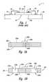
- FIG. 1schematically illustrates a conventional die and circuit board assembly 1 .
- This assembly 1includes a semiconductor die 10 having a top surface 22 a and a bottom surface 22 b .
- the bottom surface 22 bis attached via an adhesive 46 to a circuit board 40 .
- the first surface 22 a of the die 10includes multiple terminals 30 , which are used to electrically connect the die 10 to contact pads 42 on the circuit board 40 using wires 44 .
- dies 10are manufactured using an etching process (e.g., isotropic etching) and the terminals 30 are distributed across the first surface 22 a of the die 10 providing a two-dimensional array of terminals 30 .
- etching processe.g., isotropic etching
- the terminals 30As semiconductor dies 10 are made smaller, it can be necessary to make the terminals 30 smaller and/or decrease the pitch of the terminals 30 (e.g., reduce the distance between the centers of the terminals 30 ). Because of limitations on the etching process (e.g., the accuracy or precision of the process), the effective bonding area of the terminals 30 can be greatly reduced when decreasing the size and/or decreasing the pitch of the terminals 30 . The same size/pitch limitations occur on circuit boards 40 , as the size of the circuit boards 40 is reduced.
- the spacing required between the contact pads 42 on the circuit board 40 to provide structural support and to ensure proper physical and electrical separation between the contact pads 42 in a two-dimensional arraycan reduce the effective bonding area to 58 microns for a contact pad pitch of 140 microns. In many cases this effective bonding area is too small to bond the wires 44 to the contact pads 42 and a larger effective bonding area is desirable.
- a solution to these kinds of reduction in effective bonding areais to replace the etching process with a semi-additive process for producing circuit boards 40 and/or an RDL process for producing dies 10 . These processes, however, are more complex and more expensive than the etching processes currently used.
- FIG. 1is a partially schematic illustration of a conventional die and circuit board assembly in accordance with the prior art.
- FIG. 2Ais a partially schematic cross-sectional view of a microfeature workpiece during the formation process of a microelectronic device in accordance with embodiments of the invention.
- FIG. 2Bis a partially schematic cross-sectional view of the microfeature workpiece, shown in FIG. 2A , with two passageways extending between a first surface of the microfeature workpiece and a second surface of the microfeature workpiece.
- FIG. 2Cis a partially schematic cross-sectional view of the microfeature workpiece, shown in FIG. 2B , with two workpiece contacts positioned proximate to the second surface of the microfeature workpiece.
- FIG. 2Dis a partially schematic cross-sectional view of the completed microelectronic device that includes the microfeature workpiece shown in FIGS. 2A-2C .
- FIG. 3is a partially schematic cross-sectional illustration of a microelectronic device assembly in accordance with other embodiments of the invention.
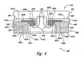
- FIG. 4is a partially schematic cross-sectional illustration of a microelectronic device assembly in accordance with still other embodiments of the invention.
- the present inventionis directed toward microelectronic devices, and associated assemblies and methods.
- certain aspects of the inventionare directed toward a microelectronic device that includes a microfeature workpiece having a side and an aperture in the side.
- the devicecan further include a workpiece contact having a surface, with at least a portion of the surface of the workpiece contact accessible through the aperture and through a passageway extending between the aperture and the surface.
- a microelectronic devicethat includes a microfeature workpiece having a first side, a second side, and a passageway.
- the passagewaycan extend through the microfeature workpiece between a first aperture in the first side and a second aperture in the second side.
- the devicecan further include a workpiece contact having a first surface and a second surface.
- the workpiece contactcan be carried by the second side and can be positioned to cover at least a portion of the second aperture.
- the workpiece contactcan also be electrically coupled to an element of the microelectronic device. At least a portion of the first surface of the workpiece contact can be positioned to be accessible through the first aperture and the passageway.
- Still other aspects of the inventionare directed toward a microelectronic device assembly that includes a support member having a first support contact and a second support contact.
- the assemblycan further include a first connector, a second connector, and a microfeature workpiece having a first side and a second side opposite the first side.
- the assemblycan still further include a first workpiece contact carried by the first side of the microfeature workpiece.
- the first workpiece contactcan be connected to the first support contact via the first connector.
- the assemblycan yet further include a second workpiece contact carried by the microfeature workpiece.
- the second workpiece contactcan be recessed from the first side and can be connected to the second support contact via the second connector.
- a microelectronic device assemblythat includes a support member having a support contact, a connector, and a microfeature workpiece having a side and an aperture in the side.
- the assemblycan further include a workpiece contact having a surface.
- the surface of the workpiece contactcan be connected to the support contact via the connector.
- the connectorcan extend through the aperture and through a passageway that extends between the aperture and the surface.
- Still other aspects of the inventionare directed toward a method for making a microelectronic device that includes positioning a workpiece contact to be recessed from a side of a microfeature workpiece.
- the methodcan further include creating a passageway extending between an aperture in the side of the microfeature workpiece and a surface of the workpiece contact. The surface of the workpiece contact can be accessible through the aperture in the side of the microfeature workpiece and the passageway.
- Yet other aspects of the inventionare directed toward a method of making a microelectronic device assembly that includes positioning a workpiece contact to be recessed from a side of a microfeature workpiece.
- the methodcan further include creating a passageway extending between an aperture in the side of the microfeature workpiece and a surface of the workpiece contact.
- the methodcan still further include connecting the surface of the workpiece contact to a support contact of a support member with a connector.
- the connectorcan extend through the aperture and through the passageway.
- Still other aspects of the inventionare directed toward a microelectronic support device that includes a support member having a first side, a second side, and a passageway extending through the support member between a first aperture in the first side and a second aperture in the second side.
- the devicecan further include a support contact having a first surface and a second surface.
- the support contactcan be carried by the second side and can be positioned to cover at least a portion of the second aperture. At least a portion of the first surface of the support contact can be positioned to be accessible through the first aperture and the passageway.
- a microelectronic support devicethat includes a support member having a side and a support contact carried by the side of the support member.
- the support contactcan be connectable to a workpiece contact of a microfeature workpiece via a connector.
- the devicecan further include recessed support contact means carried by the support member.
- the recessed support contact meanscan be connectable to a second workpiece contact of the microfeature workpiece via a bond wire.
- Still other aspects of the inventionare directed toward a microelectronic device assembly that includes a microfeature workpiece having a first workpiece contact and a second workpiece contact.
- the assemblycan further include a connector, a bond wire, a support having a side, and a first support contact carried by the side of the support.
- the first support contactcan be connected to the first workpiece contact via the first connector.
- the assemblycan further include a second support contact carried by the support and recessed from the first side. The second support contact can be connected to the second workpiece contact via the bond wire.
- microelectronic device assemblythat includes a microfeature workpiece having a first workpiece contact and a second workpiece contact.
- the assemblycan further include a connector, a bond wire, a support member having a side, and a support contact carried by the side of the support member.
- the support contactcan be connected to the first workpiece contact by the connector.
- the assemblycan further include recessed support contact means carried by the support member. The recessed support contact means can be connected to the second workpiece contact via the bond wire.
- Still other aspects of the inventionare directed toward a method for making a microelectronic support device that includes positioning a support contact to be recessed from a side of a support member.
- the methodcan further include creating a passageway extending between an aperture in the side of the support member and a surface of the support contact. The surface of the support contact can be accessible through the aperture and the passageway.
- Yet other aspects of the inventionare directed toward a method of making a microelectronic device assembly that includes positioning a support contact to be recessed from a side of a support member.
- the methodcan further include creating a passageway extending between an aperture in the side of the support member and a surface of the support contact.
- the methodcan still further include connecting the surface of the support contact to a workpiece contact of a microfeature workpiece with a bond wire extending through the aperture and through the passageway.
- microfeature workpieceand “workpiece” refer to substrates that are used to form microelectronic devices.
- Typical microdevicesinclude microelectronic circuits or components, thin-film recording heads, data storage elements, microfluidic devices; and other products.
- Micromachines and micromechanical devicesare included within this definition because they are manufactured using much of the same technology that is used in the fabrication of integrated circuits.
- the substratescan be semiconductive pieces (e.g., doped silicon wafers or gallium arsenide wafers), non-conductive pieces (e.g., various ceramic substrates), or conductive pieces.
- the workpiecesare generally round, and in other cases the workpieces have other shapes, including rectilinear shapes.
- the workpiecescan include flexible tape and/or rigid substrates.
- FIGS. 2A-2Dillustrate the formation of a microelectronic device or a microelectronic support device that has a three-dimensional array of contacts.
- the three-dimensional array of contactscan overcome the pitch limitations associated with the two-dimensional arrays of conventional dies and/or circuit boards produced using an etching process (e.g., as discussed with reference to FIG. 1 ).
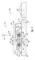
- FIG. 3is an illustration of a microelectronic device assembly having a microelectronic device with a three-dimensional array of workpiece contacts in accordance with other embodiments of the invention.
- FIG. 4is an illustration of a support member having a three-dimensional array of support contacts in accordance with still other embodiments of the invention.
- One skilled in the artwill understand that the present invention may have additional embodiments, and that other embodiments of the invention may be practiced without several of the specific features described below.
- FIG. 2Ais a partially schematic cross-sectional view of a microfeature workpiece during the formation process of a microelectronic device in accordance with embodiments of the invention.
- the microfeature workpiece 220includes a first side to 222 a and a second side 222 b .
- first and second sides 222 a , 222 bare positioned opposite one another and a first workpiece contact 230 a is carried by the first side 222 a .
- the first workpiece contact 230 aincludes a first surface 234 a and a second surface 234 b .
- the second surface 234 b of the first workpiece contact 230 ais mounted or coupled to the first side 222 a of the microfeature workpiece 220 and the first surface 234 a is accessible.
- FIG. 2Btwo passageways 224 have been formed in the microfeature workpiece 220 , shown as a first passageway 224 a and a second passageway 224 b .
- the first passagewayextends between a first aperture 226 a in the first side 222 a and a second aperture 226 b in the second side 222 b .
- the second passageway 224 bextends between a third aperture 226 c in the first side 222 a and a fourth aperture 226 d in the second side 222 b .
- the passageways 224can be formed by laser drilling (e.g., laser punching) the microfeature workpiece 220 or by using other methods well known in the art (e.g., etching, semi-additive, build-up, and/or mechanical punching techniques).
- a second workpiece contact 230 b and a third workpiece contact 230 chave been added to the microfeature workpiece.
- the second workpiece contact 230 bcan include a first surface 234 a and a second surface 234 b , and can be recessed from the first side 222 a of the microfeature workpiece 220 .
- the second workpiece contact 230 bis positioned proximate to the second aperture 226 b so that at least a portion of the first surface 234 a of the second workpiece contact 230 b is accessible through the first aperture 226 a and the first passageway 224 a .
- the second workpiece contact 230 bcan be carried by or on the second side 222 b so that the second workpiece contact 230 b partially or fully covers the second aperture 226 b .
- a portion of the first surface 234 a of the second workpiece contact 230 bis mounted to (e.g., formed in, formed on, attached to, coupled to, supported by, and/or connected to) the second side 222 b of the microfeature workpiece 220 so that the second aperture 226 b is fully covered.
- the third workpiece contact 230 ccan have a first surface 234 a and a second surface 234 b , and can be carried by the microfeature workpiece 220 .
- the third workpiece contact 230 ccan be carried proximate to the fourth aperture 226 d in a manner generally similar to the placement of the second workpiece contact 230 b relative to the second aperture 226 b . Accordingly, at least a portion of the first surface 234 a of the third workpiece contact 230 c can be accessible through a third aperture 226 c and a second passageway 224 b.
- FIG. 2Dis a partially schematic cross-sectional view of a completed microelectronic device 210 (e.g., a digital signal processor, logic chip, DRAM, flash memory, or processor) that includes the microfeature workpiece 220 discussed above with reference to FIGS. 2A-2C .
- the first, second, and third workpiece contacts 230 a , 230 b , 230 ccan be coupled or connected to at least one other element 212 (e.g., electronic elements) carried by the microfeature workpiece 220 .
- the workpiece contacts 230are coupled to the other element 212 via signal pathways 249 (e.g., wires or integrated circuitry).
- one or more of the workpiece contacts 230can be directly connected to the other element 212 without an intervening signal path 249 .
- the workpiece contacts 230can be used to connect or couple the microelectronic device 210 to external components (e.g., a support member external to the microelectronic device 210 ).
- external componentse.g., a support member external to the microelectronic device 210 .
- a portion of a connector 244e.g., a bond wire
- the connector 244extends through at least a portion of the first passageway 224 a and out of the first aperture 226 a where it can be connected to another component external to the microelectronic device 210 .
- a protective material 214(e.g., a dielectric material, encapsulant, epoxy, and/or resin) can be used to cover or encase portions of the microelectronic device 210 , including portions of the microfeature workpiece 220 , portions of the workpiece contacts 230 , and portions of the elements 212 .
- the protective material 214can provide structural integrity and/or protect portions of the microelectronic device 210 from environmental conditions (e.g., moisture, dust, and/or electromagnetic radiation).
- the second surface 234 b of the second workpiece contact 230 b , and the second surface 234 b of the third workpiece contact 230 care encased in the protective material 214 along with other portions of the microfeature workpiece 220 .
- the workpiece contacts 230can be made from various materials and include one or more portion(s).
- the second workpiece contact 230 bincludes two portions, shown as a first portion 232 a and a second portion 232 b .
- the first portion 232 acan include different materials than the second portion 232 b .
- the first portion 232 acan be made from copper and the second portion 232 b can have a nickel-gold composition (e.g., the second portion 232 b can include a layer of soft gold over nickel that prevents oxidation and facilitates connectivity to the connector 244 ).
- the first and third workpiece contacts 230 a , 230 cinclude single portions (e.g., single portions made from a copper material).
- the workpiece contacts 230can include other materials based on the desired workpiece contact characteristics (e.g., the desired conductive, protective, and/or connective properties).
- the workpiece contacts 230are distributed in three dimensions (e.g., along the X, Y, and Z axes), however, in the illustrated embodiment all of workpiece contacts 230 are accessible from the first microfeature workpiece side 222 a . This can allow the workpiece contacts 230 to be spaced closer together with respect to the X and Y axes than when the workpiece contacts 230 are carried in a two-dimensional array (e.g., as shown in FIG. 1 ).
- the surface area of the microfeature workpiece 220 required to structurally support the workpiece contacts 230can also be distributed between the first and second sides 222 a , 222 b .
- Thiscan allow peripheral, non-bonding portions of the workpiece contacts 230 (e.g., portions of the workpiece contacts 230 which are only used to structurally support the workpiece contacts 230 ) carried on different surfaces to be placed closer together relative to the X and Y axes or even overlap one another.
- placing the workpiece contacts 230 in a three-dimensional arrayalso allows vertical spacing to be used to provide physical and electrical separation between the workpiece contacts 230 .
- laser drilling techniquescan be used to precisely place the first and second passageways 224 a , 224 b , allowing the workpiece contacts 230 to be closely placed with respect to the X and Y axes. Accordingly, more workpiece contacts 230 , having a desired effective bonding area, can be placed in a given area using the three-dimensional array than can be done using the two-dimensional arrays of conventional dies produced using an etching process (e.g., as shown in FIG. 1 ). In certain embodiments, the three-dimensional array shown in FIG.
- the three-dimensional arraycan allow a workpiece contact pitch of less than 140 microns while maintaining suitable workpiece contact bonding areas.
- a feature of some of the embodiments described aboveis that a larger number of workpiece contacts, with suitable bonding areas, can be accessible from a specified area on a single side of a microelectronic device as compared to a conventional die having a two-dimensional array produced using an etching process (as shown in FIG. 1 ). Additionally, this larger number of workpiece contacts can be achieved without resorting to more complex and/or more costly processes (e.g., semi-additive or RDL processes). Accordingly, an advantage of this feature is that microelectronic devices can be made smaller without resorting to these more complex or costly production techniques and without reducing the number of available workpiece contacts.
- the microfeature workpiece 220can include more, fewer, or different arrangements of surfaces, passageways 224 , other elements 212 , and/or apertures 226 .
- the passageway(s). 224can be tapered.
- the second aperture 226 bcan be smaller than the first aperture 226 a and the first passageway 224 a can include a monotonic taper between the first and second apertures 226 a , 226 b .
- the microelectronic device 210can include more or fewer workpiece contacts 230 .
- the workpiece contactscan have more or fewer workpiece contact portions 232 , more surfaces 234 , and/or other arrangements.
- the second and third workpiece contacts 230 b , 230 ccover and extend through the corresponding apertures into the corresponding passageways 224
- the second and/or third workpiece contacts 230 b , 230 cdo not extend through the corresponding aperture(s) 226 .
- the first surface 234 a of the second workpiece contact 230 b and the first surface 234 a of the third workpiece contact 230 care positioned to be flush with, and to cover, the second and fourth apertures 226 b , 226 d , respectively.
- some of the workpiece contact(s) 230can be recessed from the first side 222 a of the microfeature workpiece 220 and accessible from the first side through passageway(s) 224 , but the recessed workpiece contacts are positioned away from the second side 222 b of the microfeature workpiece 220 (e.g., the recessed workpiece contacts 230 can be positioned internally in the microfeature workpiece 220 ).
- the microelectronic device 210includes other arrangements of protective material(s) or does not include any protective material.
- support members having recessed contactscan be replaced with support contacts and can be coupled to a support member instead of the microfeature workpiece 220 to form a microelectronic support device having recessed support contacts.
- support members and/or microelectronic supports having one or more recessed contactscan have advantages similar to those discussed above with reference to FIGS. 2A-2D .
- FIG. 3is a partially schematic cross-sectional illustration of a microelectronic device assembly 300 with a microelectronic device 310 operatively or electrically coupled to a support member 340 in accordance with embodiments of the invention.
- a microelectronic device 310 similar to the microelectronic device discussed with reference to FIGS. 2A-2Dis structurally coupled to the support member (e.g., by an adhesive 346 ).
- the microelectronic device 310includes a microfeature workpiece 320 add three workpiece contacts positioned in a three-dimensional array, shown as a first workpiece contact 330 a , a second workpiece contact 330 b , and a third workpiece contact 330 c (e.g., referred to collectively as workpiece contacts 330 ).
- Each workpiece contact 330includes a first surface 334 a and a second surface 334 b.
- the microfeature workpiece 320includes a first side 322 a and a second side 322 b , and the first workpiece contact 330 a is carried by the first side 322 a .
- the second and third workpiece contacts 330 b , 330 care positioned proximate to the second side 322 b .
- the second and third workpiece contacts 330 b , 330 care positioned so that at least a portion of the first surface 334 a of the second workpiece contact 330 b is accessible through a first passageway 324 a and at least a portion of the first surface 334 a of the third workpiece contact 330 c is accessible through a second passageway 324 b.
- first and second passageways 324 a , 324 bare tapered and the second and third workpiece contacts 330 b , 330 c have been configured to extend through at least a portion of their respective passageway 324 a , 324 b (e.g., the second and third workpiece contacts 330 b , 330 c can be “plated up” using electrostatic plating).
- a first protective material 314 acan cover at least a portion of the microfeature workpiece 320 , the second surface 334 b of the second workpiece contact 330 b , and/or the second surface 334 b of the third workpiece contact 330 c to provide structural integrity and/or protection from the environment.
- connectors 344can electrically couple the workpiece contacts 330 of the microelectronic device 310 to support contacts 342 of the support member 340 .
- a capillary 350e.g., a slimline bottle capillary, which is well known in the art
- a connector 344e.g., a wire comprised of gold
- a capillary 350 with a tip having tapered sidescan be inserted partially into the second passageway 324 b and a connector 344 can be fed though the capillary 350 to impact an end of the connector 344 against the first surface 334 a of the third workpiece contact 330 c .
- a desired mashed ball height and mashed ball diametercan be obtained.
- thermal and/or ultrasonic energycan be used to complete the bonding process.
- a molten ballcan be formed on the end of the connector 344 before the end of the connector 344 is forced against the third workpiece contact 330 c by the capillary 350 .
- an opposite end of the connector 344can then be coupled or bonded to a support contact 342 of the support member 340 in a similar manner or using other techniques.
- the first and second workpiece contacts 330 a , 330 bcan also be coupled to support contacts 342 of the support member 340 in a manner similar to that used with the third workpiece contact 330 c or by using other processes.
- the support member 340can be flexible or rigid and can have any desired configuration.
- the support member 340e.g., a printed circuit board
- the support member 340can be made with ceramic, silicon, glass, and/or organic material(s).
- the support member 340can include signal paths 349 and additional support contacts 342 that can be used to electrically connect the microelectronic device 310 to other components carried by the support member 340 or external to the support member 340 .
- a second protective material 314 bcan be placed over at least a portion of the microelectronic device 310 and/or at least a portion of the support structure 340 to provide structural integrity and/or protection from the environment.
- the microelectronic device 310 of the microelectronic device assembly 300can have a larger number of workpiece contacts (with suitable bonding areas) that are accessible from a specified area on a single side of the microfeature workpiece of the device as compared to a conventional die having a two-dimensional array produced using an etching process (as shown in FIG. 1 ). Additionally, this larger number of workpiece contacts can be provided without resorting to more complex and/or expensive manufacturing processes. Thus, as described above with respect to FIGS. 2A-2D , an advantage of this feature is that microelectronic devices can be made smaller without resorting to these more complex or costly production techniques and without reducing the number of available workpiece contacts.
- microelectronic device assembliescan be made smaller and/or more microelectronic devices to be mounted to a support member.
- Smaller microelectronic device assembliescan allow electronic devices to be made smaller and/or more powerful (e.g., a computer can be made smaller with more processing capability).
- microelectronic device assembly 310and associated methods discussed above with reference to FIG. 3 can be modified in additional embodiments of the invention.
- an adhesive 346is used to structurally couple the microelectronic device 310 to the support member 340
- the microelectronic device 310can be coupled to the support member 340 via other methods (e.g., via screw(s) and/or clip(s)).
- the microelectronic device assembly 300includes different arrangements of first and second protective materials 314 a , 314 b , more protective materials, or does not include a first and/or second protective material 314 a , 314 b .
- first and second passageways 324 a , 324 bcan be untapered or have a different tapered arrangement (e.g., tapered in two directions).
- the microelectronic device assembly 310can have various arrangements, for example, the microelectronic device assembly 310 can have a board on chip or a chip on board configuration.
- the workpiece contacts 330 of the microelectronic device 310can be coupled to the support contacts 342 of the support member 340 using other techniques.
- the capillary 350is used to bond the connectors 344 to the second and third workpiece contacts 330 b , 330 c , but the capillary 350 is not inserted into the first or second passageway 324 a , 324 b .
- a molten ballis formed on the end of the connector 344 and the connector 344 is bonded to one of the workpiece contacts 330 without using a capillary 350 .
- bonding techniqueswell known in the art are used to electrically couple or connect the workpiece contacts 330 of the microelectronic device 310 to the support contacts 342 of the support structure 340 (e.g., thermal, ultrasonic, and/or flip chip technologies).
- FIG. 4is a partially schematic cross-sectional illustration of a microelectronic device assembly 400 with a microelectronic device 410 having a microfeature workpiece 420 operatively or electrically coupled to a microelectronic support device 405 having a support member 440 in accordance with embodiments of the invention.
- the support member 440includes four support contacts positioned in a three-dimensional array, shown as a first support contact 442 a , a second support contact 442 b , a third support contact 442 c , and a fourth support contact 442 d (e.g., referred to collectively as support contacts 442 ).
- Each support contact 442includes a first surface 443 a and a second surface 443 b.
- the support member 440includes a first side 441 a and a second side 441 b , and the first and second support contacts 442 a , 442 b are carried by the first side 441 a .
- the third and fourth support contacts 442 c , 442 dare positioned proximate to the second side 441 b , with a first passageway 445 a and a second passageway 445 b , respectively.
- the third and fourth support contacts 442 c , 442 dare positioned to be recessed from the first surface or side 441 a .
- the first passageway 445 aextends between a first aperture 447 a in the first side 441 a of the support member 440 to a second aperture 447 b in the second side 441 b of the support member 440 and the second passageway 445 b extends between the first aperture 447 a and a third aperture 447 c in the second side 441 b of the support member 440 .
- FIG. 1In FIG. 1
- the third support contact 442 cis located proximate to the second aperture 447 b (e.g., covering at least a portion of the second aperture 447 b ) and extends at least partway through the second aperture 447 b and the first passageway 445 a so that at least a portion of the first surface 443 a of the third support contact 442 c is accessible through the first aperture 447 a .
- the fourth support contact 442 dis located proximate to third aperture 447 c and extends at least partway through the third aperture 447 c and the second passageway 445 b so that at least a portion of the first surface 443 a of the fourth support contact 442 d is accessible through the first aperture 447 a.
- the passageways 445 and/or support contacts 442can be tapered, as discussed above with reference to FIG. 3 .
- a first protective material 414 acan cover at least a portion of the support member 440 , the second surface 443 b of the third support contact 442 c , and/or the second surface 443 b of the fourth support contact 442 d to provide structural integrity and/or protection from the environment.
- bond wires 444can electrically couple the workpiece contacts 430 of the microelectronic device 410 to the third and fourth support contacts 442 c , 442 d .
- a capillary(discussed above with reference to FIG. 3 ) can be partially inserted through the first aperture 447 a to bond or connect the bond wire to the support contacts 442 and/or the workpiece contacts 430 .
- other bonding processescan be used.
- the microelectronic support device 405can be flexible or rigid and can have any desired configuration.
- the microelectronic support device 405e.g., a printed circuit board
- the microelectronic support device 405can be made with ceramic, silicon, glass, and/or organic material(s).
- the microelectronic support device 405can include other elements.
- the microelectronic support device 405includes signal paths 449 that connect the first and second support contacts 443 a , 443 b to the third and fourth support contacts 443 c , 443 d respectively.
- the first and second support contactscan be used to electrically connect the microelectronic support device 405 to other components carried by the microelectronic support device 405 or external to the microelectronic support device 405 .
- a second protective material 414 bcan be placed over at least a portion of the microelectronic support device 405 , the bonding wires 444 , and/or a portion of the microelectronic device 410 to provide structural integrity and/or protection from the environment.
- the microelectronic device 410can be structurally coupled to the microelectronic support device 405 (e.g., by an adhesive 446 ).
- microelectronic support device 405 and associated methods discussed above with reference to FIG. 4can be modified in additional embodiments of the invention.
- an adhesive 446is used to structurally couple the microelectronic device 410 to the microelectronic support device 405
- the microelectronic device 410can be coupled to the microelectronic support device 405 via other methods (e.g., via screw(s) and/or clip(s)).
- the microelectronic device assembly 400includes various arrangements, for example, the microelectronic device assembly 400 can have a board on chip or chip on board configuration.
- the microelectronic device assembly 400can include different combinations of first and second protective materials 414 a , 414 b , more protective materials, or does not include a first and/or second protective material 414 a , 414 b.
- a microelectronic devicecan include multiple microfeature workpieces (e.g., multiple workpieces coupled together), with at least one microfeature workpiece being configured to have one or more of the features described above.
Landscapes
- Engineering & Computer Science (AREA)
- Microelectronics & Electronic Packaging (AREA)
- Computer Hardware Design (AREA)
- Power Engineering (AREA)
- General Physics & Mathematics (AREA)
- Physics & Mathematics (AREA)
- Condensed Matter Physics & Semiconductors (AREA)
- Manufacturing & Machinery (AREA)
- Micromachines (AREA)
- Wire Bonding (AREA)
- Internal Circuitry In Semiconductor Integrated Circuit Devices (AREA)
- Jigs For Machine Tools (AREA)
- Container, Conveyance, Adherence, Positioning, Of Wafer (AREA)
Abstract
Description
- Embodiments of the present invention relate to microelectronic devices, associated assemblies, and associated methods, including microelectronic devices having a microfeature workpiece and/or a support member with one or more recessed contact(s).
- Semiconductor chips or dies are typically manufactured from a semiconductor material such as silicon, germanium, or gallium/arsenide. The dies also typically include terminals to facilitate electrical connection of the die with another electrical component. One common package design includes a semiconductor die attached to a small circuit board, e.g., via an adhesive. Some or all of the terminals of the semiconductor die may then be electrically connected to a first set of contacts of the board, e.g., by wire bonding and/o r flip chip technology. At least a portion of the connected board and die may then be encapsulated in a sealing compound to add structural integrity and/or protect portions of the die and board from environmental factors. Often a second set of contacts carried on an outer surface of the board remain exposed. These exposed contacts are electrically connected to the first contacts, allowing the features of the semiconductor die to be electrically accessed.
FIG. 1 schematically illustrates a conventional die and circuit board assembly1. This assembly1 includes asemiconductor die 10 having a top surface22aand abottom surface 22b. Thebottom surface 22bis attached via an adhesive46 to acircuit board 40. The first surface22aof the die10 includesmultiple terminals 30, which are used to electrically connect the die10 to contactpads 42 on thecircuit board 40 usingwires 44. Typically,dies 10 are manufactured using an etching process (e.g., isotropic etching) and theterminals 30 are distributed across the first surface22aof the die10 providing a two-dimensional array ofterminals 30.- As semiconductor dies10 are made smaller, it can be necessary to make the
terminals 30 smaller and/or decrease the pitch of the terminals30 (e.g., reduce the distance between the centers of the terminals30). Because of limitations on the etching process (e.g., the accuracy or precision of the process), the effective bonding area of theterminals 30 can be greatly reduced when decreasing the size and/or decreasing the pitch of theterminals 30. The same size/pitch limitations occur oncircuit boards 40, as the size of thecircuit boards 40 is reduced. For example, the spacing required between thecontact pads 42 on thecircuit board 40 to provide structural support and to ensure proper physical and electrical separation between thecontact pads 42 in a two-dimensional array can reduce the effective bonding area to58 microns for a contact pad pitch of140 microns. In many cases this effective bonding area is too small to bond thewires 44 to thecontact pads 42 and a larger effective bonding area is desirable. A solution to these kinds of reduction in effective bonding area is to replace the etching process with a semi-additive process for producingcircuit boards 40 and/or an RDL process for producingdies 10. These processes, however, are more complex and more expensive than the etching processes currently used. FIG. 1 is a partially schematic illustration of a conventional die and circuit board assembly in accordance with the prior art.FIG. 2A is a partially schematic cross-sectional view of a microfeature workpiece during the formation process of a microelectronic device in accordance with embodiments of the invention.FIG. 2B is a partially schematic cross-sectional view of the microfeature workpiece, shown inFIG. 2A , with two passageways extending between a first surface of the microfeature workpiece and a second surface of the microfeature workpiece.FIG. 2C is a partially schematic cross-sectional view of the microfeature workpiece, shown inFIG. 2B , with two workpiece contacts positioned proximate to the second surface of the microfeature workpiece.FIG. 2D is a partially schematic cross-sectional view of the completed microelectronic device that includes the microfeature workpiece shown inFIGS. 2A-2C .FIG. 3 is a partially schematic cross-sectional illustration of a microelectronic device assembly in accordance with other embodiments of the invention.FIG. 4 is a partially schematic cross-sectional illustration of a microelectronic device assembly in accordance with still other embodiments of the invention.- A. Introduction
- The present invention is directed toward microelectronic devices, and associated assemblies and methods. For example, certain aspects of the invention are directed toward a microelectronic device that includes a microfeature workpiece having a side and an aperture in the side. The device can further include a workpiece contact having a surface, with at least a portion of the surface of the workpiece contact accessible through the aperture and through a passageway extending between the aperture and the surface.
- Other aspects of the invention are directed toward a microelectronic device that includes a microfeature workpiece having a first side, a second side, and a passageway. The passageway can extend through the microfeature workpiece between a first aperture in the first side and a second aperture in the second side. The device can further include a workpiece contact having a first surface and a second surface. The workpiece contact can be carried by the second side and can be positioned to cover at least a portion of the second aperture. The workpiece contact can also be electrically coupled to an element of the microelectronic device. At least a portion of the first surface of the workpiece contact can be positioned to be accessible through the first aperture and the passageway.
- Still other aspects of the invention are directed toward a microelectronic device assembly that includes a support member having a first support contact and a second support contact. The assembly can further include a first connector, a second connector, and a microfeature workpiece having a first side and a second side opposite the first side. The assembly can still further include a first workpiece contact carried by the first side of the microfeature workpiece. The first workpiece contact can be connected to the first support contact via the first connector. The assembly can yet further include a second workpiece contact carried by the microfeature workpiece. The second workpiece contact can be recessed from the first side and can be connected to the second support contact via the second connector.
- Yet other aspects of the invention are directed toward a microelectronic device assembly that includes a support member having a support contact, a connector, and a microfeature workpiece having a side and an aperture in the side. The assembly can further include a workpiece contact having a surface. The surface of the workpiece contact can be connected to the support contact via the connector. The connector can extend through the aperture and through a passageway that extends between the aperture and the surface.
- Still other aspects of the invention are directed toward a method for making a microelectronic device that includes positioning a workpiece contact to be recessed from a side of a microfeature workpiece. The method can further include creating a passageway extending between an aperture in the side of the microfeature workpiece and a surface of the workpiece contact. The surface of the workpiece contact can be accessible through the aperture in the side of the microfeature workpiece and the passageway.
- Yet other aspects of the invention are directed toward a method of making a microelectronic device assembly that includes positioning a workpiece contact to be recessed from a side of a microfeature workpiece. The method can further include creating a passageway extending between an aperture in the side of the microfeature workpiece and a surface of the workpiece contact. The method can still further include connecting the surface of the workpiece contact to a support contact of a support member with a connector. The connector can extend through the aperture and through the passageway.
- Still other aspects of the invention are directed toward a microelectronic support device that includes a support member having a first side, a second side, and a passageway extending through the support member between a first aperture in the first side and a second aperture in the second side. The device can further include a support contact having a first surface and a second surface. The support contact can be carried by the second side and can be positioned to cover at least a portion of the second aperture. At least a portion of the first surface of the support contact can be positioned to be accessible through the first aperture and the passageway.
- Yet other aspects of the invention are directed toward a microelectronic support device that includes a support member having a side and a support contact carried by the side of the support member. The support contact can be connectable to a workpiece contact of a microfeature workpiece via a connector. The device can further include recessed support contact means carried by the support member. The recessed support contact means can be connectable to a second workpiece contact of the microfeature workpiece via a bond wire.
- Still other aspects of the invention are directed toward a microelectronic device assembly that includes a microfeature workpiece having a first workpiece contact and a second workpiece contact. The assembly can further include a connector, a bond wire, a support having a side, and a first support contact carried by the side of the support. The first support contact can be connected to the first workpiece contact via the first connector. The assembly can further include a second support contact carried by the support and recessed from the first side. The second support contact can be connected to the second workpiece contact via the bond wire.
- Yet other aspects of the invention can include a microelectronic device assembly that includes a microfeature workpiece having a first workpiece contact and a second workpiece contact. The assembly can further include a connector, a bond wire, a support member having a side, and a support contact carried by the side of the support member. The support contact can be connected to the first workpiece contact by the connector. The assembly can further include recessed support contact means carried by the support member. The recessed support contact means can be connected to the second workpiece contact via the bond wire.
- Still other aspects of the invention are directed toward a method for making a microelectronic support device that includes positioning a support contact to be recessed from a side of a support member. The method can further include creating a passageway extending between an aperture in the side of the support member and a surface of the support contact. The surface of the support contact can be accessible through the aperture and the passageway.
- Yet other aspects of the invention are directed toward a method of making a microelectronic device assembly that includes positioning a support contact to be recessed from a side of a support member. The method can further include creating a passageway extending between an aperture in the side of the support member and a surface of the support contact. The method can still further include connecting the surface of the support contact to a workpiece contact of a microfeature workpiece with a bond wire extending through the aperture and through the passageway.
- As used herein, the terms “microfeature workpiece” and “workpiece” refer to substrates that are used to form microelectronic devices. Typical microdevices include microelectronic circuits or components, thin-film recording heads, data storage elements, microfluidic devices; and other products. Micromachines and micromechanical devices are included within this definition because they are manufactured using much of the same technology that is used in the fabrication of integrated circuits. The substrates can be semiconductive pieces (e.g., doped silicon wafers or gallium arsenide wafers), non-conductive pieces (e.g., various ceramic substrates), or conductive pieces. In some cases, the workpieces are generally round, and in other cases the workpieces have other shapes, including rectilinear shapes. The workpieces can include flexible tape and/or rigid substrates.
- Several specific details of the invention are set forth in the following description and in
FIGS. 2A-4 to provide a thorough understanding of certain embodiments of the invention. For example,FIGS. 2A-2D illustrate the formation of a microelectronic device or a microelectronic support device that has a three-dimensional array of contacts. In certain embodiments, the three-dimensional array of contacts can overcome the pitch limitations associated with the two-dimensional arrays of conventional dies and/or circuit boards produced using an etching process (e.g., as discussed with reference toFIG. 1 ).FIG. 3 is an illustration of a microelectronic device assembly having a microelectronic device with a three-dimensional array of workpiece contacts in accordance with other embodiments of the invention.FIG. 4 is an illustration of a support member having a three-dimensional array of support contacts in accordance with still other embodiments of the invention. One skilled in the art, however, will understand that the present invention may have additional embodiments, and that other embodiments of the invention may be practiced without several of the specific features described below. - B. Microelectronic Devices and Associated Methods
FIG. 2A is a partially schematic cross-sectional view of a microfeature workpiece during the formation process of a microelectronic device in accordance with embodiments of the invention. For the purpose of illustration, the formation of the microelectronic device will be discussed in terms of a microfeature workpiece, however, one skilled in the art will understand that this process can apply equally to a the formation of one or more contacts on a microelectronic support device and/or a support member, as discussed in greater detail with reference toFIG. 4 . Themicrofeature workpiece 220 includes a first side to222aand asecond side 222b. In the illustrated embodiment, the first andsecond sides first workpiece contact 230ais carried by thefirst side 222a. Thefirst workpiece contact 230aincludes afirst surface 234aand asecond surface 234b. InFIG. 2A , thesecond surface 234bof thefirst workpiece contact 230ais mounted or coupled to thefirst side 222aof themicrofeature workpiece 220 and thefirst surface 234ais accessible.- In
FIG. 2B twopassageways 224 have been formed in themicrofeature workpiece 220, shown as afirst passageway 224aand asecond passageway 224b. The first passageway extends between afirst aperture 226ain thefirst side 222aand asecond aperture 226bin thesecond side 222b. Thesecond passageway 224bextends between athird aperture 226cin thefirst side 222aand afourth aperture 226d in thesecond side 222b. Thepassageways 224 can be formed by laser drilling (e.g., laser punching) themicrofeature workpiece 220 or by using other methods well known in the art (e.g., etching, semi-additive, build-up, and/or mechanical punching techniques). - In
FIG. 2C , asecond workpiece contact 230band athird workpiece contact 230chave been added to the microfeature workpiece. Thesecond workpiece contact 230bcan include afirst surface 234aand asecond surface 234b, and can be recessed from thefirst side 222aof themicrofeature workpiece 220. In the illustrated embodiment, thesecond workpiece contact 230bis positioned proximate to thesecond aperture 226bso that at least a portion of thefirst surface 234aof thesecond workpiece contact 230bis accessible through thefirst aperture 226aand thefirst passageway 224a. For example, thesecond workpiece contact 230bcan be carried by or on thesecond side 222bso that thesecond workpiece contact 230bpartially or fully covers thesecond aperture 226b. In the illustrated embodiment, a portion of thefirst surface 234aof thesecond workpiece contact 230bis mounted to (e.g., formed in, formed on, attached to, coupled to, supported by, and/or connected to) thesecond side 222bof themicrofeature workpiece 220 so that thesecond aperture 226bis fully covered. - The
third workpiece contact 230ccan have afirst surface 234aand asecond surface 234b, and can be carried by themicrofeature workpiece 220. In the illustrated embodiment, thethird workpiece contact 230ccan be carried proximate to thefourth aperture 226d in a manner generally similar to the placement of thesecond workpiece contact 230brelative to thesecond aperture 226b. Accordingly, at least a portion of thefirst surface 234aof thethird workpiece contact 230ccan be accessible through athird aperture 226cand asecond passageway 224b. FIG. 2D is a partially schematic cross-sectional view of a completed microelectronic device210 (e.g., a digital signal processor, logic chip, DRAM, flash memory, or processor) that includes themicrofeature workpiece 220 discussed above with reference toFIGS. 2A-2C . In the illustrated embodiment, the first, second, andthird workpiece contacts microfeature workpiece 220. In the illustrated embodiment, the workpiece contacts230 are coupled to theother element 212 via signal pathways249 (e.g., wires or integrated circuitry). In other embodiments, one or more of the workpiece contacts230 can be directly connected to theother element 212 without an interveningsignal path 249.- The workpiece contacts230 can be used to connect or couple the
microelectronic device 210 to external components (e.g., a support member external to the microelectronic device210). In the illustrated embodiment, a portion of a connector244 (e.g., a bond wire) is shown coupled, attached, or connected to thefirst surface 234aof thesecond workpiece contact 230b. Theconnector 244 extends through at least a portion of thefirst passageway 224aand out of thefirst aperture 226awhere it can be connected to another component external to themicroelectronic device 210. - A protective material214 (e.g., a dielectric material, encapsulant, epoxy, and/or resin) can be used to cover or encase portions of the
microelectronic device 210, including portions of themicrofeature workpiece 220, portions of the workpiece contacts230, and portions of theelements 212. In various embodiments, theprotective material 214 can provide structural integrity and/or protect portions of themicroelectronic device 210 from environmental conditions (e.g., moisture, dust, and/or electromagnetic radiation). For example, in the illustrated embodiment thesecond surface 234bof thesecond workpiece contact 230b, and thesecond surface 234bof thethird workpiece contact 230care encased in theprotective material 214 along with other portions of themicrofeature workpiece 220. - Additionally, the workpiece contacts230 can be made from various materials and include one or more portion(s). For example, in the illustrated embodiment the
second workpiece contact 230bincludes two portions, shown as afirst portion 232aand asecond portion 232b. In certain embodiments, thefirst portion 232acan include different materials than thesecond portion 232b. For example, in one embodiment thefirst portion 232acan be made from copper and thesecond portion 232bcan have a nickel-gold composition (e.g., thesecond portion 232bcan include a layer of soft gold over nickel that prevents oxidation and facilitates connectivity to the connector244). In the illustrated embodiment, the first andthird workpiece contacts - By distributing the workpiece contacts230 between the first and
second sides microfeature workpiece side 222a. This can allow the workpiece contacts230 to be spaced closer together with respect to the X and Y axes than when the workpiece contacts230 are carried in a two-dimensional array (e.g., as shown inFIG. 1 ). For example, because the workpiece contacts230 can be staggered between the first andsecond sides microfeature workpiece 220 required to structurally support the workpiece contacts230 can also be distributed between the first andsecond sides - Additionally, placing the workpiece contacts230 in a three-dimensional array also allows vertical spacing to be used to provide physical and electrical separation between the workpiece contacts230. Furthermore, laser drilling techniques can be used to precisely place the first and
second passageways FIG. 1 ). In certain embodiments, the three-dimensional array shown inFIG. 2D can allow three workpiece contacts230, with usable effective bonding areas, to be accessible via the same surface area that is required to carry two workpiece contacts230 in the two-dimensional array used on conventional dies. For example, in certain embodiments the three-dimensional array can allow a workpiece contact pitch of less than 140 microns while maintaining suitable workpiece contact bonding areas. - Accordingly, a feature of some of the embodiments described above is that a larger number of workpiece contacts, with suitable bonding areas, can be accessible from a specified area on a single side of a microelectronic device as compared to a conventional die having a two-dimensional array produced using an etching process (as shown in
FIG. 1 ). Additionally, this larger number of workpiece contacts can be achieved without resorting to more complex and/or more costly processes (e.g., semi-additive or RDL processes). Accordingly, an advantage of this feature is that microelectronic devices can be made smaller without resorting to these more complex or costly production techniques and without reducing the number of available workpiece contacts. - The embodiments of the
microelectronic device 210 and associated methods discussed above with reference toFIGS. 2A-2D can be modified in additional embodiments of the invention. For example, in other embodiments themicrofeature workpiece 220 can include more, fewer, or different arrangements of surfaces,passageways 224,other elements 212, and/orapertures 226. For instance, in certain embodiments the passageway(s).224 can be tapered. For example, in one embodiment thesecond aperture 226bcan be smaller than thefirst aperture 226aand thefirst passageway 224acan include a monotonic taper between the first andsecond apertures microelectronic device 210 can include more or fewer workpiece contacts230. - In yet other embodiments, the workpiece contacts can have more or fewer
workpiece contact portions 232,more surfaces 234, and/or other arrangements. For example, although in the illustrated embodiment the second andthird workpiece contacts passageways 224, in other embodiments the second and/orthird workpiece contacts first surface 234aof thesecond workpiece contact 230band thefirst surface 234aof thethird workpiece contact 230care positioned to be flush with, and to cover, the second andfourth apertures first side 222aof themicrofeature workpiece 220 and accessible from the first side through passageway(s)224, but the recessed workpiece contacts are positioned away from thesecond side 222bof the microfeature workpiece220 (e.g., the recessed workpiece contacts230 can be positioned internally in the microfeature workpiece220). In yet other embodiments, themicroelectronic device 210 includes other arrangements of protective material(s) or does not include any protective material. - As discussed above, the concepts, processes, and apparatuses discussed above with reference to
FIGS. 2A-2D apply equally to support members having recessed contacts. For example, in other embodiments the workpiece contacts230 can be replaced with support contacts and can be coupled to a support member instead of themicrofeature workpiece 220 to form a microelectronic support device having recessed support contacts. Additionally, support members and/or microelectronic supports having one or more recessed contacts, can have advantages similar to those discussed above with reference toFIGS. 2A-2D . - C. Microelectronic Device Assemblies and Associated Methods
FIG. 3 is a partially schematic cross-sectional illustration of amicroelectronic device assembly 300 with amicroelectronic device 310 operatively or electrically coupled to asupport member 340 in accordance with embodiments of the invention. In the illustrated embodiment, amicroelectronic device 310 similar to the microelectronic device discussed with reference toFIGS. 2A-2D is structurally coupled to the support member (e.g., by an adhesive346). Themicroelectronic device 310 includes amicrofeature workpiece 320 add three workpiece contacts positioned in a three-dimensional array, shown as afirst workpiece contact 330a, asecond workpiece contact 330b, and athird workpiece contact 330c(e.g., referred to collectively as workpiece contacts330). Eachworkpiece contact 330 includes afirst surface 334aand asecond surface 334b.- In the illustrated embodiment, the
microfeature workpiece 320 includes afirst side 322aand asecond side 322b, and thefirst workpiece contact 330ais carried by thefirst side 322a. InFIG. 3 , the second andthird workpiece contacts second side 322b. Additionally, the second andthird workpiece contacts first surface 334aof thesecond workpiece contact 330bis accessible through afirst passageway 324aand at least a portion of thefirst surface 334aof thethird workpiece contact 330cis accessible through asecond passageway 324b. - In the illustrated embodiment, the first and
second passageways third workpiece contacts respective passageway third workpiece contacts third workpiece contacts tapered passageways connector 344 must extend into the first andsecond passageways protective material 314acan cover at least a portion of themicrofeature workpiece 320, thesecond surface 334bof thesecond workpiece contact 330b, and/or thesecond surface 334bof thethird workpiece contact 330cto provide structural integrity and/or protection from the environment. - In the illustrated embodiment, connectors344 (e.g., bonding wires or solder balls) can electrically couple the
workpiece contacts 330 of themicroelectronic device 310 to supportcontacts 342 of thesupport member 340. For example, a capillary350 (e.g., a slimline bottle capillary, which is well known in the art) can be partially inserted into thesecond passageway 324band a connector344 (e.g., a wire comprised of gold) can be fed through the capillary and bonded to thethird workpiece contact 330c. For example, a capillary350 with a tip having tapered sides (e.g., sides with a ten degree taper) can be inserted partially into thesecond passageway 324band aconnector 344 can be fed though the capillary350 to impact an end of theconnector 344 against thefirst surface 334aof thethird workpiece contact 330c. By managing the amount the capillary is inserted into thesecond passageway 324band the impact force of the end of theconnector 344 against thethird workpiece contact 330c, a desired mashed ball height and mashed ball diameter can be obtained. Additionally, thermal and/or ultrasonic energy can be used to complete the bonding process. In certain embodiments, a molten ball can be formed on the end of theconnector 344 before the end of theconnector 344 is forced against thethird workpiece contact 330cby thecapillary 350. In any case, an opposite end of theconnector 344 can then be coupled or bonded to asupport contact 342 of thesupport member 340 in a similar manner or using other techniques. The first andsecond workpiece contacts contacts 342 of thesupport member 340 in a manner similar to that used with thethird workpiece contact 330cor by using other processes. - The
support member 340 can be flexible or rigid and can have any desired configuration. For example, the support member340 (e.g., a printed circuit board) can be made with ceramic, silicon, glass, and/or organic material(s). Additionally, thesupport member 340 can include signalpaths 349 andadditional support contacts 342 that can be used to electrically connect themicroelectronic device 310 to other components carried by thesupport member 340 or external to thesupport member 340. In certain embodiments, once theworkpiece contacts 330 of themicroelectronic device 310 are coupled to therespective support contacts 342 of thesupport member 340, a secondprotective material 314bcan be placed over at least a portion of themicroelectronic device 310 and/or at least a portion of thesupport structure 340 to provide structural integrity and/or protection from the environment. - As discussed above with reference to
FIGS. 2A-2D , themicroelectronic device 310 of themicroelectronic device assembly 300 can have a larger number of workpiece contacts (with suitable bonding areas) that are accessible from a specified area on a single side of the microfeature workpiece of the device as compared to a conventional die having a two-dimensional array produced using an etching process (as shown inFIG. 1 ). Additionally, this larger number of workpiece contacts can be provided without resorting to more complex and/or expensive manufacturing processes. Thus, as described above with respect toFIGS. 2A-2D , an advantage of this feature is that microelectronic devices can be made smaller without resorting to these more complex or costly production techniques and without reducing the number of available workpiece contacts. This in turn, can allow microelectronic device assemblies to be made smaller and/or more microelectronic devices to be mounted to a support member. Smaller microelectronic device assemblies can allow electronic devices to be made smaller and/or more powerful (e.g., a computer can be made smaller with more processing capability). - The embodiments of the
microelectronic device assembly 310 and associated methods discussed above with reference toFIG. 3 can be modified in additional embodiments of the invention. For example, although in the illustrated embodiment an adhesive346 is used to structurally couple themicroelectronic device 310 to thesupport member 340, in other embodiments themicroelectronic device 310 can be coupled to thesupport member 340 via other methods (e.g., via screw(s) and/or clip(s)). In still other embodiments, themicroelectronic device assembly 300 includes different arrangements of first and secondprotective materials protective material second passageways microelectronic device assembly 310 can have various arrangements, for example, themicroelectronic device assembly 310 can have a board on chip or a chip on board configuration. - In still other embodiments, the
workpiece contacts 330 of themicroelectronic device 310 can be coupled to thesupport contacts 342 of thesupport member 340 using other techniques. For example, in other embodiments the capillary350 is used to bond theconnectors 344 to the second andthird workpiece contacts second passageway connector 344 and theconnector 344 is bonded to one of theworkpiece contacts 330 without using acapillary 350. In yet other embodiments, other bonding techniques well known in the art are used to electrically couple or connect theworkpiece contacts 330 of themicroelectronic device 310 to thesupport contacts 342 of the support structure340 (e.g., thermal, ultrasonic, and/or flip chip technologies). - As discussed above, in other embodiments a support member can include one or more recessed contacts. Accordingly,
FIG. 4 is a partially schematic cross-sectional illustration of amicroelectronic device assembly 400 with amicroelectronic device 410 having amicrofeature workpiece 420 operatively or electrically coupled to amicroelectronic support device 405 having asupport member 440 in accordance with embodiments of the invention. Thesupport member 440 includes four support contacts positioned in a three-dimensional array, shown as afirst support contact 442a, asecond support contact 442b, athird support contact 442c, and afourth support contact 442d(e.g., referred to collectively as support contacts442). Each support contact442 includes afirst surface 443aand asecond surface 443b. - In the illustrated embodiment, the
support member 440 includes afirst side 441aand asecond side 441b, and the first andsecond support contacts first side 441a. InFIG. 4 , the third andfourth support contacts second side 441b, with afirst passageway 445aand asecond passageway 445b, respectively. Additionally, the third andfourth support contacts side 441a. For example, in the illustrated embodiment thefirst passageway 445aextends between afirst aperture 447ain thefirst side 441 a of thesupport member 440 to asecond aperture 447bin thesecond side 441bof thesupport member 440 and thesecond passageway 445bextends between thefirst aperture 447aand athird aperture 447cin thesecond side 441bof thesupport member 440. InFIG. 4 , thethird support contact 442cis located proximate to thesecond aperture 447b(e.g., covering at least a portion of thesecond aperture 447b) and extends at least partway through thesecond aperture 447band thefirst passageway 445aso that at least a portion of thefirst surface 443aof thethird support contact 442cis accessible through thefirst aperture 447a. Similarly, in the illustrated embodiment, thefourth support contact 442dis located proximate tothird aperture 447cand extends at least partway through thethird aperture 447cand thesecond passageway 445bso that at least a portion of thefirst surface 443aof thefourth support contact 442dis accessible through thefirst aperture 447a. - In other embodiments, the passageways445 and/or support contacts442 can be tapered, as discussed above with reference to
FIG. 3 . In other embodiments, a firstprotective material 414acan cover at least a portion of thesupport member 440, thesecond surface 443bof thethird support contact 442c, and/or thesecond surface 443bof thefourth support contact 442dto provide structural integrity and/or protection from the environment. - In the illustrated embodiment,
bond wires 444 can electrically couple theworkpiece contacts 430 of themicroelectronic device 410 to the third andfourth support contacts FIG. 3 ) can be partially inserted through thefirst aperture 447ato bond or connect the bond wire to the support contacts442 and/or theworkpiece contacts 430. In other embodiments, other bonding processes can be used. - The
microelectronic support device 405 can be flexible or rigid and can have any desired configuration. For example, the microelectronic support device405 (e.g., a printed circuit board) can be made with ceramic, silicon, glass, and/or organic material(s). Additionally, themicroelectronic support device 405 can include other elements. For example, in the illustrated embodiment themicroelectronic support device 405 includessignal paths 449 that connect the first andsecond support contacts microelectronic support device 405 to other components carried by themicroelectronic support device 405 or external to themicroelectronic support device 405. - In certain embodiments, once the
workpiece contacts 430 of themicroelectronic device 410 are coupled to the third andfourth support contacts protective material 414bcan be placed over at least a portion of themicroelectronic support device 405, thebonding wires 444, and/or a portion of themicroelectronic device 410 to provide structural integrity and/or protection from the environment. Additionally, in certain embodiments themicroelectronic device 410 can be structurally coupled to the microelectronic support device405 (e.g., by an adhesive446). Some embodiments of themicroelectronic support device 405, discussed with reference toFIG. 4 can have features and advantages similar to those discussed with reference toFIGS. 2A-3 . - The embodiments of the
microelectronic support device 405 and associated methods discussed above with reference toFIG. 4 can be modified in additional embodiments of the invention. For example, although in the illustrated embodiment an adhesive446 is used to structurally couple themicroelectronic device 410 to themicroelectronic support device 405, in other embodiments themicroelectronic device 410 can be coupled to themicroelectronic support device 405 via other methods (e.g., via screw(s) and/or clip(s)). In still~other embodiments, themicroelectronic device assembly 400 includes various arrangements, for example, themicroelectronic device assembly 400 can have a board on chip or chip on board configuration. In yet other embodiments, themicroelectronic device assembly 400 can include different combinations of first and secondprotective materials protective material - From the foregoing, it will be appreciated -that specific embodiments of the invention have been described herein for purposes of illustration, but that various modifications may be made without deviating from the invention. Additionally, aspects of the invention described in the context of particular embodiments may be combined or eliminated in other embodiments. For example, in other embodiments a microelectronic device can include multiple microfeature workpieces (e.g., multiple workpieces coupled together), with at least one microfeature workpiece being configured to have one or more of the features described above. Although advantages associated with certain embodiments of the invention have been described in the context of those embodiments, other embodiments may also exhibit such advantages. Additionally, not all embodiments need necessarily exhibit such advantages to fall within the scope of the invention. Accordingly, the invention is not limited except as by the appended claims.
Claims (46)
Priority Applications (3)
| Application Number | Priority Date | Filing Date | Title |
|---|---|---|---|
| US11/617,567US7968369B2 (en) | 2005-08-24 | 2006-12-28 | Microelectronic devices and microelectronic support devices, and associated assemblies and methods |
| US13/171,137US8778732B2 (en) | 2005-08-24 | 2011-06-28 | Microelectronic devices and microelectronic support devices, and associated assemblies and methods |
| US14/331,722US9129862B2 (en) | 2005-08-24 | 2014-07-15 | Microelectronic devices and microelectronic support devices, and associated assemblies and methods |
Applications Claiming Priority (2)
| Application Number | Priority Date | Filing Date | Title |
|---|---|---|---|
| SG200505410-1ASG130061A1 (en) | 2005-08-24 | 2005-08-24 | Microelectronic devices and microelectronic support devices, and associated assemblies and methods |
| SG200505410-1 | 2005-08-24 |
Related Child Applications (1)
| Application Number | Title | Priority Date | Filing Date |
|---|---|---|---|
| US11/617,567DivisionUS7968369B2 (en) | 2005-08-24 | 2006-12-28 | Microelectronic devices and microelectronic support devices, and associated assemblies and methods |
Publications (2)
| Publication Number | Publication Date |
|---|---|
| US20070045797A1true US20070045797A1 (en) | 2007-03-01 |
| US8174101B2 US8174101B2 (en) | 2012-05-08 |
Family
ID=37681670
Family Applications (4)
| Application Number | Title | Priority Date | Filing Date |
|---|---|---|---|
| US11/218,256Active2028-01-06US8174101B2 (en) | 2005-08-24 | 2005-09-01 | Microelectronic devices and microelectronic support devices, and associated assemblies and methods |
| US11/617,567Active2027-10-05US7968369B2 (en) | 2005-08-24 | 2006-12-28 | Microelectronic devices and microelectronic support devices, and associated assemblies and methods |
| US13/171,137Active2027-01-13US8778732B2 (en) | 2005-08-24 | 2011-06-28 | Microelectronic devices and microelectronic support devices, and associated assemblies and methods |
| US14/331,722Expired - LifetimeUS9129862B2 (en) | 2005-08-24 | 2014-07-15 | Microelectronic devices and microelectronic support devices, and associated assemblies and methods |
Family Applications After (3)
| Application Number | Title | Priority Date | Filing Date |
|---|---|---|---|
| US11/617,567Active2027-10-05US7968369B2 (en) | 2005-08-24 | 2006-12-28 | Microelectronic devices and microelectronic support devices, and associated assemblies and methods |
| US13/171,137Active2027-01-13US8778732B2 (en) | 2005-08-24 | 2011-06-28 | Microelectronic devices and microelectronic support devices, and associated assemblies and methods |
| US14/331,722Expired - LifetimeUS9129862B2 (en) | 2005-08-24 | 2014-07-15 | Microelectronic devices and microelectronic support devices, and associated assemblies and methods |
Country Status (7)
| Country | Link |
|---|---|
| US (4) | US8174101B2 (en) |
| EP (1) | EP1929520B1 (en) |
| JP (1) | JP2009506539A (en) |
| KR (1) | KR101000646B1 (en) |
| SG (1) | SG130061A1 (en) |
| TW (1) | TWI314773B (en) |
| WO (1) | WO2007024526A2 (en) |
Cited By (2)
| Publication number | Priority date | Publication date | Assignee | Title |
|---|---|---|---|---|
| US8778732B2 (en) | 2005-08-24 | 2014-07-15 | Micron Technology, Inc. | Microelectronic devices and microelectronic support devices, and associated assemblies and methods |
| US20240079306A1 (en)* | 2022-09-07 | 2024-03-07 | Micron Technology, Inc. | Microelectronic device packages and related methods and systems |
Families Citing this family (12)
| Publication number | Priority date | Publication date | Assignee | Title |
|---|---|---|---|---|
| US7645789B2 (en)* | 2006-04-07 | 2010-01-12 | Vertex Pharmaceuticals Incorporated | Indole derivatives as CFTR modulators |
| KR100935854B1 (en) | 2009-09-22 | 2010-01-08 | 테세라 리써치 엘엘씨 | Microelectronic assembly with impedance controlled wirebond and reference wirebond |
| KR100950511B1 (en) | 2009-09-22 | 2010-03-30 | 테세라 리써치 엘엘씨 | Microelectronic assembly with impedance controlled wirebond and conductive reference element |
| US8853708B2 (en) | 2010-09-16 | 2014-10-07 | Tessera, Inc. | Stacked multi-die packages with impedance control |
| US8222725B2 (en) | 2010-09-16 | 2012-07-17 | Tessera, Inc. | Metal can impedance control structure |
| US9136197B2 (en) | 2010-09-16 | 2015-09-15 | Tessera, Inc. | Impedence controlled packages with metal sheet or 2-layer RDL |
| US8581377B2 (en) | 2010-09-16 | 2013-11-12 | Tessera, Inc. | TSOP with impedance control |
| US8786083B2 (en) | 2010-09-16 | 2014-07-22 | Tessera, Inc. | Impedance controlled packages with metal sheet or 2-layer RDL |
| US9123713B2 (en) | 2010-11-24 | 2015-09-01 | Tessera, Inc. | Lead structures with vertical offsets |
| KR101061531B1 (en)* | 2010-12-17 | 2011-09-01 | 테세라 리써치 엘엘씨 | Enhanced stacked microelectronic assemblies with central contacts and improved ground or power distribution |
| US10325876B2 (en)* | 2014-06-25 | 2019-06-18 | Nxp Usa, Inc. | Surface finish for wirebonding |
| US9761562B2 (en) | 2015-05-06 | 2017-09-12 | Micron Technology, Inc. | Semiconductor device packages including a controller element |
Citations (86)
| Publication number | Priority date | Publication date | Assignee | Title |
|---|---|---|---|---|
| US4807021A (en)* | 1986-03-10 | 1989-02-21 | Kabushiki Kaisha Toshiba | Semiconductor device having stacking structure |
| US5062565A (en)* | 1990-07-13 | 1991-11-05 | Micron Technology, Inc. | Method for combining die attach and wirebond in the assembly of a semiconductor package |
| US5128831A (en)* | 1991-10-31 | 1992-07-07 | Micron Technology, Inc. | High-density electronic package comprising stacked sub-modules which are electrically interconnected by solder-filled vias |
| US5252857A (en)* | 1991-08-05 | 1993-10-12 | International Business Machines Corporation | Stacked DCA memory chips |
| US5518957A (en)* | 1991-10-10 | 1996-05-21 | Samsung Electronics Co., Ltd. | Method for making a thin profile semiconductor package |
| USRE35385E (en)* | 1988-12-12 | 1996-12-03 | Sgs-Thomson Microelectronics, Sa. | Method for fixing an electronic component and its contacts to a support |
| US5593927A (en)* | 1993-10-14 | 1997-01-14 | Micron Technology, Inc. | Method for packaging semiconductor dice |
| US5739050A (en)* | 1996-01-26 | 1998-04-14 | Micron Technology, Inc. | Method and apparatus for assembling a semiconductor package for testing |
| US5815000A (en)* | 1991-06-04 | 1998-09-29 | Micron Technology, Inc. | Method for testing semiconductor dice with conventionally sized temporary packages |
| US5883426A (en)* | 1996-04-18 | 1999-03-16 | Nec Corporation | Stack module |
| US5891797A (en)* | 1997-10-20 | 1999-04-06 | Micron Technology, Inc. | Method of forming a support structure for air bridge wiring of an integrated circuit |
| US5894218A (en)* | 1994-04-18 | 1999-04-13 | Micron Technology, Inc. | Method and apparatus for automatically positioning electronic dice within component packages |
| US5946553A (en)* | 1991-06-04 | 1999-08-31 | Micron Technology, Inc. | Process for manufacturing a semiconductor package with bi-substrate die |
| US5986209A (en)* | 1997-07-09 | 1999-11-16 | Micron Technology, Inc. | Package stack via bottom leaded plastic (BLP) packaging |
| US5990566A (en)* | 1998-05-20 | 1999-11-23 | Micron Technology, Inc. | High density semiconductor package |
| US6011694A (en)* | 1996-08-01 | 2000-01-04 | Fuji Machinery Mfg. & Electronics Co., Ltd. | Ball grid array semiconductor package with solder ball openings in an insulative base |
| US6018249A (en)* | 1997-12-11 | 2000-01-25 | Micron Technolgoy, Inc. | Test system with mechanical alignment for semiconductor chip scale packages and dice |
| US6020629A (en)* | 1998-06-05 | 2000-02-01 | Micron Technology, Inc. | Stacked semiconductor package and method of fabrication |
| US6025728A (en)* | 1997-04-25 | 2000-02-15 | Micron Technology, Inc. | Semiconductor package with wire bond protective member |
| US6028365A (en)* | 1998-03-30 | 2000-02-22 | Micron Technology, Inc. | Integrated circuit package and method of fabrication |
| US6048744A (en)* | 1997-09-15 | 2000-04-11 | Micron Technology, Inc. | Integrated circuit package alignment feature |
| US6051878A (en)* | 1997-03-10 | 2000-04-18 | Micron Technology, Inc. | Method of constructing stacked packages |
| US6072233A (en)* | 1998-05-04 | 2000-06-06 | Micron Technology, Inc. | Stackable ball grid array package |
| US6072236A (en)* | 1996-03-07 | 2000-06-06 | Micron Technology, Inc. | Micromachined chip scale package |
| US6072323A (en)* | 1997-03-03 | 2000-06-06 | Micron Technology, Inc. | Temporary package, and method system for testing semiconductor dice having backside electrodes |
| US6081429A (en)* | 1999-01-20 | 2000-06-27 | Micron Technology, Inc. | Test interposer for use with ball grid array packages assemblies and ball grid array packages including same and methods |
| US6089920A (en)* | 1998-05-04 | 2000-07-18 | Micron Technology, Inc. | Modular die sockets with flexible interconnects for packaging bare semiconductor die |
| US6094058A (en)* | 1991-06-04 | 2000-07-25 | Micron Technology, Inc. | Temporary semiconductor package having dense array external contacts |
| US6097087A (en)* | 1997-10-31 | 2000-08-01 | Micron Technology, Inc. | Semiconductor package including flex circuit, interconnects and dense array external contacts |
| US6107122A (en)* | 1997-08-04 | 2000-08-22 | Micron Technology, Inc. | Direct die contact (DDC) semiconductor package |
| US6130474A (en)* | 1996-12-30 | 2000-10-10 | Micron Technology, Inc. | Leads under chip IC package |
| US6148509A (en)* | 1997-04-07 | 2000-11-21 | Micron Technology, Inc. | Method for supporting an integrated circuit die |
| US6165887A (en)* | 1997-04-22 | 2000-12-26 | Micron Technology , Inc. | Method of improving interconnect of semiconductor devices by using a flattened ball bond |
| US6163956A (en)* | 1998-02-23 | 2000-12-26 | Micron Technology, Inc. | Method of making chip scale package with heat spreade |
| US6175149B1 (en)* | 1998-02-13 | 2001-01-16 | Micron Technology, Inc. | Mounting multiple semiconductor dies in a package |
| US6188232B1 (en)* | 1996-12-31 | 2001-02-13 | Micron Technology, Inc. | Temporary package, system, and method for testing semiconductor dice and chip scale packages |
| US6198172B1 (en)* | 1997-02-20 | 2001-03-06 | Micron Technology, Inc. | Semiconductor chip package |
| US6201304B1 (en)* | 1995-12-19 | 2001-03-13 | Micron Technology, Inc. | Flip chip adaptor package for bare die |
| US6208156B1 (en)* | 1998-09-03 | 2001-03-27 | Micron Technology, Inc. | Test carrier for packaging semiconductor components having contact balls and calibration carrier for calibrating semiconductor test systems |
| US6214716B1 (en)* | 1998-09-30 | 2001-04-10 | Micron Technology, Inc. | Semiconductor substrate-based BGA interconnection and methods of farication same |
| US6212767B1 (en)* | 1999-08-31 | 2001-04-10 | Micron Technology, Inc. | Assembling a stacked die package |
| US6225689B1 (en)* | 1998-08-21 | 2001-05-01 | Micron Technology, Inc. | Low profile multi-IC chip package connector |
| US6232666B1 (en)* | 1998-12-04 | 2001-05-15 | Mciron Technology, Inc. | Interconnect for packaging semiconductor dice and fabricating BGA packages |
| US6235554B1 (en)* | 1995-11-27 | 2001-05-22 | Micron Technology, Inc. | Method for fabricating stackable chip scale semiconductor package |
| US6239489B1 (en)* | 1999-07-30 | 2001-05-29 | Micron Technology, Inc. | Reinforcement of lead bonding in microelectronics packages |
| US6247629B1 (en)* | 1997-09-08 | 2001-06-19 | Micron Technology, Inc. | Wire bond monitoring system for layered packages |
| US6255833B1 (en)* | 1997-03-04 | 2001-07-03 | Micron Technology, Inc. | Method for testing semiconductor dice and chip scale packages |
| US6258624B1 (en)* | 2000-01-10 | 2001-07-10 | Micron Technology, Inc. | Semiconductor package having downset leadframe for reducing package bow |
| US6259153B1 (en)* | 1998-08-20 | 2001-07-10 | Micron Technology, Inc. | Transverse hybrid LOC package |
| US6261865B1 (en)* | 1998-10-06 | 2001-07-17 | Micron Technology, Inc. | Multi chip semiconductor package and method of construction |
| US6281042B1 (en)* | 1998-08-31 | 2001-08-28 | Micron Technology, Inc. | Structure and method for a high performance electronic packaging assembly |
| US6281577B1 (en)* | 1996-06-28 | 2001-08-28 | Pac Tech-Packaging Technologies Gmbh | Chips arranged in plurality of planes and electrically connected to one another |
| US6285204B1 (en)* | 1996-03-19 | 2001-09-04 | Micron Technology, Inc. | Method for testing semiconductor packages using oxide penetrating test contacts |
| US6294839B1 (en)* | 1999-08-30 | 2001-09-25 | Micron Technology, Inc. | Apparatus and methods of packaging and testing die |
| US6297547B1 (en)* | 1998-02-13 | 2001-10-02 | Micron Technology Inc. | Mounting multiple semiconductor dies in a package |
| US6303981B1 (en)* | 1999-09-01 | 2001-10-16 | Micron Technology, Inc. | Semiconductor package having stacked dice and leadframes and method of fabrication |
| US6326698B1 (en)* | 2000-06-08 | 2001-12-04 | Micron Technology, Inc. | Semiconductor devices having protective layers thereon through which contact pads are exposed and stereolithographic methods of fabricating such semiconductor devices |
| US6331221B1 (en)* | 1998-04-15 | 2001-12-18 | Micron Technology, Inc. | Process for providing electrical connection between a semiconductor die and a semiconductor die receiving member |
| US20020041027A1 (en)* | 2000-10-10 | 2002-04-11 | Kabushiki Kaisha Toshiba | Semiconductor device |
| US6429528B1 (en)* | 1998-02-27 | 2002-08-06 | Micron Technology, Inc. | Multichip semiconductor package |
| US6437586B1 (en)* | 1997-11-03 | 2002-08-20 | Micron Technology, Inc. | Load board socket adapter and interface method |
| US20020155728A1 (en)* | 1990-09-24 | 2002-10-24 | Tessera, Inc. | Semiconductor chip assemblies, methods of making same and components for same |
| US6483044B1 (en)* | 2000-08-23 | 2002-11-19 | Micron Technology, Inc. | Interconnecting substrates for electrical coupling of microelectronic components |
| US20030049882A1 (en)* | 2001-08-29 | 2003-03-13 | Yin Leng Nam | Wire bonded microelectronic device assemblies and methods of manufacturing same |
| US20030062631A1 (en)* | 2001-09-28 | 2003-04-03 | Mitsubishi Denki Kabushiki Kaisha | Semiconductor device and method of fabricating the same |
| US6548376B2 (en)* | 2001-08-30 | 2003-04-15 | Micron Technology, Inc. | Methods of thinning microelectronic workpieces |
| US6552910B1 (en)* | 2000-06-28 | 2003-04-22 | Micron Technology, Inc. | Stacked-die assemblies with a plurality of microelectronic devices and methods of manufacture |
| US20030080428A1 (en)* | 2001-11-01 | 2003-05-01 | Mitsubishi Denki Kabushiki | Semiconductor device |
| US6560117B2 (en)* | 2000-06-28 | 2003-05-06 | Micron Technology, Inc. | Packaged microelectronic die assemblies and methods of manufacture |
| US20030151139A1 (en)* | 2002-02-13 | 2003-08-14 | Nec Electronics Corporation | Semiconductor device |
| US6607937B1 (en)* | 2000-08-23 | 2003-08-19 | Micron Technology, Inc. | Stacked microelectronic dies and methods for stacking microelectronic dies |
| US6614092B2 (en)* | 2000-08-16 | 2003-09-02 | Micron Technology, Inc. | Microelectronic device package with conductive elements and associated method of manufacture |
| US20040125579A1 (en)* | 2002-12-27 | 2004-07-01 | Satoru Konishi | Semiconductor module |
| US20050098605A1 (en)* | 2003-11-06 | 2005-05-12 | International Business Machines Corporation | Apparatus and method for low pressure wirebond |
| US20050104228A1 (en)* | 2003-11-13 | 2005-05-19 | Rigg Sidney B. | Microelectronic devices, methods for forming vias in microelectronic devices, and methods for packaging microelectronic devices |
| US20050104171A1 (en)* | 2003-11-13 | 2005-05-19 | Benson Peter A. | Microelectronic devices having conductive complementary structures and methods of manufacturing microelectronic devices having conductive complementary structures |
| US20050127478A1 (en)* | 2003-12-10 | 2005-06-16 | Hiatt William M. | Microelectronic devices and methods for filling vias in microelectronic devices |
| US20050187850A1 (en)* | 2004-02-25 | 2005-08-25 | Stuart Horowitz | Method for efficient investment and distribution of assets |
| US20050253245A1 (en)* | 2004-05-12 | 2005-11-17 | Mark Lynch | Package design and method for electrically connecting die to package |
| US6975035B2 (en)* | 2002-03-04 | 2005-12-13 | Micron Technology, Inc. | Method and apparatus for dielectric filling of flip chip on interposer assembly |
| US20050287783A1 (en)* | 2004-06-29 | 2005-12-29 | Kirby Kyle K | Microelectronic devices and methods for forming interconnects in microelectronic devices |
| US20060108666A1 (en)* | 2004-11-25 | 2006-05-25 | Shinko Electric Industries Co., Ltd. | Semiconductor device and method of fabricating the same |
| US20060261340A1 (en)* | 2004-06-14 | 2006-11-23 | Farnworth Warren M | Microelectronic imagers and methods of packaging microelectronic imagers |
| US7180149B2 (en)* | 2003-08-28 | 2007-02-20 | Fujikura Ltd. | Semiconductor package with through-hole |
| US20070105272A1 (en)* | 2005-08-24 | 2007-05-10 | Micron Technology, Inc. | Microelectronic devices and microelectronic support devices, and associated assemblies and methods |
| US7517790B2 (en)* | 2002-10-31 | 2009-04-14 | International Business Machines Corporation | Method and structure to enhance temperature/humidity/bias performance of semiconductor devices by surface modification |
Family Cites Families (12)
| Publication number | Priority date | Publication date | Assignee | Title |
|---|---|---|---|---|
| DE19536278A1 (en)* | 1995-09-28 | 1997-04-03 | Ods Gmbh & Co Kg | Carrier element for integrated circuit element of e.g. chip card |
| US6861290B1 (en)* | 1995-12-19 | 2005-03-01 | Micron Technology, Inc. | Flip-chip adaptor package for bare die |
| JP2001044357A (en) | 1999-07-26 | 2001-02-16 | Seiko Epson Corp | Semiconductor device and method of manufacturing the same |
| JP2001308122A (en) | 2000-04-18 | 2001-11-02 | Shinko Electric Ind Co Ltd | Method of manufacturing semiconductor device |
| US6531335B1 (en)* | 2000-04-28 | 2003-03-11 | Micron Technology, Inc. | Interposers including upwardly protruding dams, semiconductor device assemblies including the interposers, and methods |
| JP2002107382A (en)* | 2000-09-27 | 2002-04-10 | Asahi Kasei Corp | Semiconductor device, method of manufacturing the same, and current sensor |
| JP2002261194A (en)* | 2001-02-28 | 2002-09-13 | Mitsumi Electric Co Ltd | Semiconductor device |
| JP2003017495A (en) | 2001-07-04 | 2003-01-17 | Matsushita Electric Ind Co Ltd | Semiconductor device and method of manufacturing the same |
| JP2004281982A (en) | 2003-03-19 | 2004-10-07 | Seiko Epson Corp | Semiconductor device and manufacturing method thereof |
| JP2005101067A (en) | 2003-09-22 | 2005-04-14 | Sharp Corp | Substrate wiring structure and wiring forming method |
| US7393770B2 (en)* | 2005-05-19 | 2008-07-01 | Micron Technology, Inc. | Backside method for fabricating semiconductor components with conductive interconnects |
| US7994622B2 (en)* | 2007-04-16 | 2011-08-09 | Tessera, Inc. | Microelectronic packages having cavities for receiving microelectric elements |
- 2005
- 2005-08-24SGSG200505410-1Apatent/SG130061A1/enunknown
- 2005-09-01USUS11/218,256patent/US8174101B2/enactiveActive
- 2006
- 2006-08-11WOPCT/US2006/031600patent/WO2007024526A2/enactiveApplication Filing
- 2006-08-11EPEP06801402.6Apatent/EP1929520B1/enactiveActive
- 2006-08-11JPJP2008527969Apatent/JP2009506539A/enactivePending
- 2006-08-11KRKR20087006163Apatent/KR101000646B1/enactiveActive
- 2006-08-23TWTW95130920Apatent/TWI314773B/enactive
- 2006-12-28USUS11/617,567patent/US7968369B2/enactiveActive
- 2011
- 2011-06-28USUS13/171,137patent/US8778732B2/enactiveActive
- 2014
- 2014-07-15USUS14/331,722patent/US9129862B2/ennot_activeExpired - Lifetime
Patent Citations (93)
| Publication number | Priority date | Publication date | Assignee | Title |
|---|---|---|---|---|
| US4807021A (en)* | 1986-03-10 | 1989-02-21 | Kabushiki Kaisha Toshiba | Semiconductor device having stacking structure |
| USRE35385E (en)* | 1988-12-12 | 1996-12-03 | Sgs-Thomson Microelectronics, Sa. | Method for fixing an electronic component and its contacts to a support |
| US5062565A (en)* | 1990-07-13 | 1991-11-05 | Micron Technology, Inc. | Method for combining die attach and wirebond in the assembly of a semiconductor package |
| US20020155728A1 (en)* | 1990-09-24 | 2002-10-24 | Tessera, Inc. | Semiconductor chip assemblies, methods of making same and components for same |
| US5946553A (en)* | 1991-06-04 | 1999-08-31 | Micron Technology, Inc. | Process for manufacturing a semiconductor package with bi-substrate die |
| US5815000A (en)* | 1991-06-04 | 1998-09-29 | Micron Technology, Inc. | Method for testing semiconductor dice with conventionally sized temporary packages |
| US6094058A (en)* | 1991-06-04 | 2000-07-25 | Micron Technology, Inc. | Temporary semiconductor package having dense array external contacts |
| US6020624A (en)* | 1991-06-04 | 2000-02-01 | Micron Technology, Inc. | Semiconductor package with bi-substrate die |
| US5252857A (en)* | 1991-08-05 | 1993-10-12 | International Business Machines Corporation | Stacked DCA memory chips |
| US5518957A (en)* | 1991-10-10 | 1996-05-21 | Samsung Electronics Co., Ltd. | Method for making a thin profile semiconductor package |
| US5128831A (en)* | 1991-10-31 | 1992-07-07 | Micron Technology, Inc. | High-density electronic package comprising stacked sub-modules which are electrically interconnected by solder-filled vias |
| US5593927A (en)* | 1993-10-14 | 1997-01-14 | Micron Technology, Inc. | Method for packaging semiconductor dice |
| US5894218A (en)* | 1994-04-18 | 1999-04-13 | Micron Technology, Inc. | Method and apparatus for automatically positioning electronic dice within component packages |
| US6235554B1 (en)* | 1995-11-27 | 2001-05-22 | Micron Technology, Inc. | Method for fabricating stackable chip scale semiconductor package |
| US6265766B1 (en)* | 1995-12-19 | 2001-07-24 | Micron Technology, Inc. | Flip chip adaptor package for bare die |
| US6201304B1 (en)* | 1995-12-19 | 2001-03-13 | Micron Technology, Inc. | Flip chip adaptor package for bare die |
| US5739050A (en)* | 1996-01-26 | 1998-04-14 | Micron Technology, Inc. | Method and apparatus for assembling a semiconductor package for testing |
| US6072236A (en)* | 1996-03-07 | 2000-06-06 | Micron Technology, Inc. | Micromachined chip scale package |
| US6285204B1 (en)* | 1996-03-19 | 2001-09-04 | Micron Technology, Inc. | Method for testing semiconductor packages using oxide penetrating test contacts |
| US5883426A (en)* | 1996-04-18 | 1999-03-16 | Nec Corporation | Stack module |
| US6281577B1 (en)* | 1996-06-28 | 2001-08-28 | Pac Tech-Packaging Technologies Gmbh | Chips arranged in plurality of planes and electrically connected to one another |
| US6011694A (en)* | 1996-08-01 | 2000-01-04 | Fuji Machinery Mfg. & Electronics Co., Ltd. | Ball grid array semiconductor package with solder ball openings in an insulative base |
| US6130474A (en)* | 1996-12-30 | 2000-10-10 | Micron Technology, Inc. | Leads under chip IC package |
| US6188232B1 (en)* | 1996-12-31 | 2001-02-13 | Micron Technology, Inc. | Temporary package, system, and method for testing semiconductor dice and chip scale packages |
| US6198172B1 (en)* | 1997-02-20 | 2001-03-06 | Micron Technology, Inc. | Semiconductor chip package |
| US6072323A (en)* | 1997-03-03 | 2000-06-06 | Micron Technology, Inc. | Temporary package, and method system for testing semiconductor dice having backside electrodes |
| US6255833B1 (en)* | 1997-03-04 | 2001-07-03 | Micron Technology, Inc. | Method for testing semiconductor dice and chip scale packages |
| US6051878A (en)* | 1997-03-10 | 2000-04-18 | Micron Technology, Inc. | Method of constructing stacked packages |
| US6148509A (en)* | 1997-04-07 | 2000-11-21 | Micron Technology, Inc. | Method for supporting an integrated circuit die |
| US6165887A (en)* | 1997-04-22 | 2000-12-26 | Micron Technology , Inc. | Method of improving interconnect of semiconductor devices by using a flattened ball bond |
| US6025728A (en)* | 1997-04-25 | 2000-02-15 | Micron Technology, Inc. | Semiconductor package with wire bond protective member |
| US5986209A (en)* | 1997-07-09 | 1999-11-16 | Micron Technology, Inc. | Package stack via bottom leaded plastic (BLP) packaging |
| US6150717A (en)* | 1997-08-04 | 2000-11-21 | Micron Technology, Inc. | Direct die contact (DDC) semiconductor package |
| US6107122A (en)* | 1997-08-04 | 2000-08-22 | Micron Technology, Inc. | Direct die contact (DDC) semiconductor package |
| US6247629B1 (en)* | 1997-09-08 | 2001-06-19 | Micron Technology, Inc. | Wire bond monitoring system for layered packages |
| US6048744A (en)* | 1997-09-15 | 2000-04-11 | Micron Technology, Inc. | Integrated circuit package alignment feature |
| US5891797A (en)* | 1997-10-20 | 1999-04-06 | Micron Technology, Inc. | Method of forming a support structure for air bridge wiring of an integrated circuit |
| US6097087A (en)* | 1997-10-31 | 2000-08-01 | Micron Technology, Inc. | Semiconductor package including flex circuit, interconnects and dense array external contacts |
| US6437586B1 (en)* | 1997-11-03 | 2002-08-20 | Micron Technology, Inc. | Load board socket adapter and interface method |
| US6018249A (en)* | 1997-12-11 | 2000-01-25 | Micron Technolgoy, Inc. | Test system with mechanical alignment for semiconductor chip scale packages and dice |
| US6175149B1 (en)* | 1998-02-13 | 2001-01-16 | Micron Technology, Inc. | Mounting multiple semiconductor dies in a package |
| US6297547B1 (en)* | 1998-02-13 | 2001-10-02 | Micron Technology Inc. | Mounting multiple semiconductor dies in a package |
| US6163956A (en)* | 1998-02-23 | 2000-12-26 | Micron Technology, Inc. | Method of making chip scale package with heat spreade |
| US6429528B1 (en)* | 1998-02-27 | 2002-08-06 | Micron Technology, Inc. | Multichip semiconductor package |
| US6028365A (en)* | 1998-03-30 | 2000-02-22 | Micron Technology, Inc. | Integrated circuit package and method of fabrication |
| US6331221B1 (en)* | 1998-04-15 | 2001-12-18 | Micron Technology, Inc. | Process for providing electrical connection between a semiconductor die and a semiconductor die receiving member |
| US6089920A (en)* | 1998-05-04 | 2000-07-18 | Micron Technology, Inc. | Modular die sockets with flexible interconnects for packaging bare semiconductor die |
| US6072233A (en)* | 1998-05-04 | 2000-06-06 | Micron Technology, Inc. | Stackable ball grid array package |
| US5990566A (en)* | 1998-05-20 | 1999-11-23 | Micron Technology, Inc. | High density semiconductor package |
| US6020629A (en)* | 1998-06-05 | 2000-02-01 | Micron Technology, Inc. | Stacked semiconductor package and method of fabrication |
| US6259153B1 (en)* | 1998-08-20 | 2001-07-10 | Micron Technology, Inc. | Transverse hybrid LOC package |
| US6225689B1 (en)* | 1998-08-21 | 2001-05-01 | Micron Technology, Inc. | Low profile multi-IC chip package connector |
| US6258623B1 (en)* | 1998-08-21 | 2001-07-10 | Micron Technology, Inc. | Low profile multi-IC chip package connector |
| US6281042B1 (en)* | 1998-08-31 | 2001-08-28 | Micron Technology, Inc. | Structure and method for a high performance electronic packaging assembly |
| US6208156B1 (en)* | 1998-09-03 | 2001-03-27 | Micron Technology, Inc. | Test carrier for packaging semiconductor components having contact balls and calibration carrier for calibrating semiconductor test systems |
| US6214716B1 (en)* | 1998-09-30 | 2001-04-10 | Micron Technology, Inc. | Semiconductor substrate-based BGA interconnection and methods of farication same |
| US6261865B1 (en)* | 1998-10-06 | 2001-07-17 | Micron Technology, Inc. | Multi chip semiconductor package and method of construction |
| US6329222B1 (en)* | 1998-12-04 | 2001-12-11 | Micron Technology, Inc. | Interconnect for packaging semiconductor dice and fabricating BGA packages |
| US6232666B1 (en)* | 1998-12-04 | 2001-05-15 | Mciron Technology, Inc. | Interconnect for packaging semiconductor dice and fabricating BGA packages |
| US6081429A (en)* | 1999-01-20 | 2000-06-27 | Micron Technology, Inc. | Test interposer for use with ball grid array packages assemblies and ball grid array packages including same and methods |
| US6239489B1 (en)* | 1999-07-30 | 2001-05-29 | Micron Technology, Inc. | Reinforcement of lead bonding in microelectronics packages |
| US6294839B1 (en)* | 1999-08-30 | 2001-09-25 | Micron Technology, Inc. | Apparatus and methods of packaging and testing die |
| US6212767B1 (en)* | 1999-08-31 | 2001-04-10 | Micron Technology, Inc. | Assembling a stacked die package |
| US6303981B1 (en)* | 1999-09-01 | 2001-10-16 | Micron Technology, Inc. | Semiconductor package having stacked dice and leadframes and method of fabrication |
| US6258624B1 (en)* | 2000-01-10 | 2001-07-10 | Micron Technology, Inc. | Semiconductor package having downset leadframe for reducing package bow |
| US6326698B1 (en)* | 2000-06-08 | 2001-12-04 | Micron Technology, Inc. | Semiconductor devices having protective layers thereon through which contact pads are exposed and stereolithographic methods of fabricating such semiconductor devices |
| US6552910B1 (en)* | 2000-06-28 | 2003-04-22 | Micron Technology, Inc. | Stacked-die assemblies with a plurality of microelectronic devices and methods of manufacture |
| US6560117B2 (en)* | 2000-06-28 | 2003-05-06 | Micron Technology, Inc. | Packaged microelectronic die assemblies and methods of manufacture |
| US6614092B2 (en)* | 2000-08-16 | 2003-09-02 | Micron Technology, Inc. | Microelectronic device package with conductive elements and associated method of manufacture |
| US6483044B1 (en)* | 2000-08-23 | 2002-11-19 | Micron Technology, Inc. | Interconnecting substrates for electrical coupling of microelectronic components |
| US6607937B1 (en)* | 2000-08-23 | 2003-08-19 | Micron Technology, Inc. | Stacked microelectronic dies and methods for stacking microelectronic dies |
| US20020041027A1 (en)* | 2000-10-10 | 2002-04-11 | Kabushiki Kaisha Toshiba | Semiconductor device |
| US20030049882A1 (en)* | 2001-08-29 | 2003-03-13 | Yin Leng Nam | Wire bonded microelectronic device assemblies and methods of manufacturing same |
| US6650013B2 (en)* | 2001-08-29 | 2003-11-18 | Micron Technology, Inc. | Method of manufacturing wire bonded microelectronic device assemblies |
| US6548376B2 (en)* | 2001-08-30 | 2003-04-15 | Micron Technology, Inc. | Methods of thinning microelectronic workpieces |
| US20030062631A1 (en)* | 2001-09-28 | 2003-04-03 | Mitsubishi Denki Kabushiki Kaisha | Semiconductor device and method of fabricating the same |
| US20030080428A1 (en)* | 2001-11-01 | 2003-05-01 | Mitsubishi Denki Kabushiki | Semiconductor device |
| US20030151139A1 (en)* | 2002-02-13 | 2003-08-14 | Nec Electronics Corporation | Semiconductor device |
| US6975035B2 (en)* | 2002-03-04 | 2005-12-13 | Micron Technology, Inc. | Method and apparatus for dielectric filling of flip chip on interposer assembly |
| US7517790B2 (en)* | 2002-10-31 | 2009-04-14 | International Business Machines Corporation | Method and structure to enhance temperature/humidity/bias performance of semiconductor devices by surface modification |
| US20040125579A1 (en)* | 2002-12-27 | 2004-07-01 | Satoru Konishi | Semiconductor module |
| US7180149B2 (en)* | 2003-08-28 | 2007-02-20 | Fujikura Ltd. | Semiconductor package with through-hole |
| US20050098605A1 (en)* | 2003-11-06 | 2005-05-12 | International Business Machines Corporation | Apparatus and method for low pressure wirebond |
| US20050104228A1 (en)* | 2003-11-13 | 2005-05-19 | Rigg Sidney B. | Microelectronic devices, methods for forming vias in microelectronic devices, and methods for packaging microelectronic devices |
| US20050104171A1 (en)* | 2003-11-13 | 2005-05-19 | Benson Peter A. | Microelectronic devices having conductive complementary structures and methods of manufacturing microelectronic devices having conductive complementary structures |
| US20050127478A1 (en)* | 2003-12-10 | 2005-06-16 | Hiatt William M. | Microelectronic devices and methods for filling vias in microelectronic devices |
| US20050187850A1 (en)* | 2004-02-25 | 2005-08-25 | Stuart Horowitz | Method for efficient investment and distribution of assets |
| US20050253245A1 (en)* | 2004-05-12 | 2005-11-17 | Mark Lynch | Package design and method for electrically connecting die to package |
| US20060261340A1 (en)* | 2004-06-14 | 2006-11-23 | Farnworth Warren M | Microelectronic imagers and methods of packaging microelectronic imagers |
| US20050287783A1 (en)* | 2004-06-29 | 2005-12-29 | Kirby Kyle K | Microelectronic devices and methods for forming interconnects in microelectronic devices |
| US20060108666A1 (en)* | 2004-11-25 | 2006-05-25 | Shinko Electric Industries Co., Ltd. | Semiconductor device and method of fabricating the same |
| US20070105272A1 (en)* | 2005-08-24 | 2007-05-10 | Micron Technology, Inc. | Microelectronic devices and microelectronic support devices, and associated assemblies and methods |
| US20110252623A1 (en)* | 2005-08-24 | 2011-10-20 | Micron Technology, Inc. | Microelectronic devices and microelectronic support devices, and associated assemblies and methods |
Cited By (4)
| Publication number | Priority date | Publication date | Assignee | Title |
|---|---|---|---|---|
| US8778732B2 (en) | 2005-08-24 | 2014-07-15 | Micron Technology, Inc. | Microelectronic devices and microelectronic support devices, and associated assemblies and methods |
| US9129862B2 (en) | 2005-08-24 | 2015-09-08 | Micron Technology, Inc. | Microelectronic devices and microelectronic support devices, and associated assemblies and methods |
| US20240079306A1 (en)* | 2022-09-07 | 2024-03-07 | Micron Technology, Inc. | Microelectronic device packages and related methods and systems |
| US12374612B2 (en)* | 2022-09-07 | 2025-07-29 | Micron Technology, Inc. | Microelectronic device packages and related methods and systems |
Also Published As
| Publication number | Publication date |
|---|---|
| US20140326488A1 (en) | 2014-11-06 |
| SG130061A1 (en) | 2007-03-20 |
| US9129862B2 (en) | 2015-09-08 |
| US20070105272A1 (en) | 2007-05-10 |
| TWI314773B (en) | 2009-09-11 |
| US20110252623A1 (en) | 2011-10-20 |
| JP2009506539A (en) | 2009-02-12 |
| KR20080038219A (en) | 2008-05-02 |
| US8778732B2 (en) | 2014-07-15 |
| US7968369B2 (en) | 2011-06-28 |
| EP1929520A2 (en) | 2008-06-11 |
| EP1929520B1 (en) | 2016-03-23 |
| US8174101B2 (en) | 2012-05-08 |
| WO2007024526A2 (en) | 2007-03-01 |
| WO2007024526A3 (en) | 2007-04-19 |
| KR101000646B1 (en) | 2010-12-10 |
Similar Documents
| Publication | Publication Date | Title |
|---|---|---|
| US9129862B2 (en) | Microelectronic devices and microelectronic support devices, and associated assemblies and methods | |
| US11721614B2 (en) | Method of manufacturing semiconductor devices and corresponding semiconductor device having vias and pads formed by laser | |
| US6664615B1 (en) | Method and apparatus for lead-frame based grid array IC packaging | |
| TWI692030B (en) | Semiconductor package and method of manufacturing the same | |
| US9806061B2 (en) | Bumpless wafer level fan-out package | |
| US6835599B2 (en) | Method for fabricating semiconductor component with multi layered leadframe | |
| CN202534641U (en) | Packaged electronic device | |
| US7564137B2 (en) | Stackable integrated circuit structures and systems devices and methods related thereto | |
| EP2005470B1 (en) | Lead frame based, over-molded semiconductor package with integrated through hole technology (tht) heat spreader pin(s) and associated method of manufacturing | |
| US20180342434A1 (en) | Method of manufacturing semiconductor devices and corresponding semiconductor device | |
| US20170194249A1 (en) | Package substrate and method of fabricating the same | |
| CN101826501A (en) | High density contact pin-less integrated circuit element | |
| KR20090122283A (en) | A device for packaging a semiconductor device, a packaged semiconductor component, a method for manufacturing a device for packaging a semiconductor device, and a method for manufacturing a semiconductor component | |
| EP2005469B1 (en) | Method of making a carrierless chip package for integrated circuit devices | |
| US5989935A (en) | Column grid array for semiconductor packaging and method | |
| JP2006173493A (en) | Semiconductor device and manufacturing method therefor | |
| US20110062586A1 (en) | Chip for Reliable Stacking on another Chip | |
| US9842807B2 (en) | Integrated circuit assembly | |
| JP4881369B2 (en) | Manufacturing method of semiconductor device | |
| JP4819398B2 (en) | Electronic module | |
| KR20050054010A (en) | Interposer attaching method used in manufacturing process for stack type semiconductor chip package |
Legal Events
| Date | Code | Title | Description |
|---|---|---|---|
| AS | Assignment | Owner name:MICRON TECHNOLOGY, INC., IDAHO Free format text:ASSIGNMENT OF ASSIGNORS INTEREST;ASSIGNORS:LEE, TECK KHENG;CHAI, DAVID YIH MING;NG, HONG WAN;SIGNING DATES FROM 20051116 TO 20051122;REEL/FRAME:017415/0722 Owner name:MICRON TECHNOLOGY, INC., IDAHO Free format text:ASSIGNMENT OF ASSIGNORS INTEREST;ASSIGNORS:LEE, TECK KHENG;CHAI, DAVID YIH MING;NG, HONG WAN;REEL/FRAME:017415/0722;SIGNING DATES FROM 20051116 TO 20051122 | |
| FEPP | Fee payment procedure | Free format text:PAYOR NUMBER ASSIGNED (ORIGINAL EVENT CODE: ASPN); ENTITY STATUS OF PATENT OWNER: LARGE ENTITY | |
| STCF | Information on status: patent grant | Free format text:PATENTED CASE | |
| CC | Certificate of correction | ||
| FPAY | Fee payment | Year of fee payment:4 | |
| AS | Assignment | Owner name:U.S. BANK NATIONAL ASSOCIATION, AS COLLATERAL AGENT, CALIFORNIA Free format text:SECURITY INTEREST;ASSIGNOR:MICRON TECHNOLOGY, INC.;REEL/FRAME:038669/0001 Effective date:20160426 Owner name:U.S. BANK NATIONAL ASSOCIATION, AS COLLATERAL AGEN Free format text:SECURITY INTEREST;ASSIGNOR:MICRON TECHNOLOGY, INC.;REEL/FRAME:038669/0001 Effective date:20160426 | |
| AS | Assignment | Owner name:MORGAN STANLEY SENIOR FUNDING, INC., AS COLLATERAL AGENT, MARYLAND Free format text:PATENT SECURITY AGREEMENT;ASSIGNOR:MICRON TECHNOLOGY, INC.;REEL/FRAME:038954/0001 Effective date:20160426 Owner name:MORGAN STANLEY SENIOR FUNDING, INC., AS COLLATERAL Free format text:PATENT SECURITY AGREEMENT;ASSIGNOR:MICRON TECHNOLOGY, INC.;REEL/FRAME:038954/0001 Effective date:20160426 | |
| AS | Assignment | Owner name:U.S. BANK NATIONAL ASSOCIATION, AS COLLATERAL AGENT, CALIFORNIA Free format text:CORRECTIVE ASSIGNMENT TO CORRECT THE REPLACE ERRONEOUSLY FILED PATENT #7358718 WITH THE CORRECT PATENT #7358178 PREVIOUSLY RECORDED ON REEL 038669 FRAME 0001. ASSIGNOR(S) HEREBY CONFIRMS THE SECURITY INTEREST;ASSIGNOR:MICRON TECHNOLOGY, INC.;REEL/FRAME:043079/0001 Effective date:20160426 Owner name:U.S. BANK NATIONAL ASSOCIATION, AS COLLATERAL AGEN Free format text:CORRECTIVE ASSIGNMENT TO CORRECT THE REPLACE ERRONEOUSLY FILED PATENT #7358718 WITH THE CORRECT PATENT #7358178 PREVIOUSLY RECORDED ON REEL 038669 FRAME 0001. ASSIGNOR(S) HEREBY CONFIRMS THE SECURITY INTEREST;ASSIGNOR:MICRON TECHNOLOGY, INC.;REEL/FRAME:043079/0001 Effective date:20160426 | |
| AS | Assignment | Owner name:JPMORGAN CHASE BANK, N.A., AS COLLATERAL AGENT, ILLINOIS Free format text:SECURITY INTEREST;ASSIGNORS:MICRON TECHNOLOGY, INC.;MICRON SEMICONDUCTOR PRODUCTS, INC.;REEL/FRAME:047540/0001 Effective date:20180703 Owner name:JPMORGAN CHASE BANK, N.A., AS COLLATERAL AGENT, IL Free format text:SECURITY INTEREST;ASSIGNORS:MICRON TECHNOLOGY, INC.;MICRON SEMICONDUCTOR PRODUCTS, INC.;REEL/FRAME:047540/0001 Effective date:20180703 | |
| AS | Assignment | Owner name:MICRON TECHNOLOGY, INC., IDAHO Free format text:RELEASE BY SECURED PARTY;ASSIGNOR:U.S. BANK NATIONAL ASSOCIATION, AS COLLATERAL AGENT;REEL/FRAME:047243/0001 Effective date:20180629 | |
| AS | Assignment | Owner name:MICRON TECHNOLOGY, INC., IDAHO Free format text:RELEASE BY SECURED PARTY;ASSIGNOR:MORGAN STANLEY SENIOR FUNDING, INC., AS COLLATERAL AGENT;REEL/FRAME:050937/0001 Effective date:20190731 | |
| MAFP | Maintenance fee payment | Free format text:PAYMENT OF MAINTENANCE FEE, 8TH YEAR, LARGE ENTITY (ORIGINAL EVENT CODE: M1552); ENTITY STATUS OF PATENT OWNER: LARGE ENTITY Year of fee payment:8 | |
| AS | Assignment | Owner name:MICRON SEMICONDUCTOR PRODUCTS, INC., IDAHO Free format text:RELEASE BY SECURED PARTY;ASSIGNOR:JPMORGAN CHASE BANK, N.A., AS COLLATERAL AGENT;REEL/FRAME:051028/0001 Effective date:20190731 Owner name:MICRON TECHNOLOGY, INC., IDAHO Free format text:RELEASE BY SECURED PARTY;ASSIGNOR:JPMORGAN CHASE BANK, N.A., AS COLLATERAL AGENT;REEL/FRAME:051028/0001 Effective date:20190731 | |
| MAFP | Maintenance fee payment | Free format text:PAYMENT OF MAINTENANCE FEE, 12TH YEAR, LARGE ENTITY (ORIGINAL EVENT CODE: M1553); ENTITY STATUS OF PATENT OWNER: LARGE ENTITY Year of fee payment:12 |