US20070045779A1 - Methods for forming through-wafer interconnects, intermediate structures so formed, and devices and systems having at least one solder dam structure - Google Patents
Methods for forming through-wafer interconnects, intermediate structures so formed, and devices and systems having at least one solder dam structureDownload PDFInfo
- Publication number
- US20070045779A1 US20070045779A1US11/218,705US21870505AUS2007045779A1US 20070045779 A1US20070045779 A1US 20070045779A1US 21870505 AUS21870505 AUS 21870505AUS 2007045779 A1US2007045779 A1US 2007045779A1
- Authority
- US
- United States
- Prior art keywords
- solder
- forming
- substrate
- blind
- blind hole
- Prior art date
- Legal status (The legal status is an assumption and is not a legal conclusion. Google has not performed a legal analysis and makes no representation as to the accuracy of the status listed.)
- Granted
Links
- 229910000679solderInorganic materials0.000titleclaimsabstractdescription175
- 238000000034methodMethods0.000titleclaimsabstractdescription133
- 239000000758substrateSubstances0.000claimsabstractdescription121
- 239000004065semiconductorSubstances0.000claimsabstractdescription90
- PXHVJJICTQNCMI-UHFFFAOYSA-NNickelChemical compound[Ni]PXHVJJICTQNCMI-UHFFFAOYSA-N0.000claimsabstractdescription59
- 239000000463materialSubstances0.000claimsabstractdescription56
- 238000009736wettingMethods0.000claimsabstractdescription31
- 229910052759nickelInorganic materials0.000claimsabstractdescription30
- 230000009477glass transitionEffects0.000claimsabstractdescription24
- 229910052751metalInorganic materials0.000claimsabstractdescription22
- 239000002184metalSubstances0.000claimsabstractdescription22
- 238000000151depositionMethods0.000claimsdescription32
- 238000002161passivationMethods0.000claimsdescription30
- VYPSYNLAJGMNEJ-UHFFFAOYSA-NSilicium dioxideChemical compoundO=[Si]=OVYPSYNLAJGMNEJ-UHFFFAOYSA-N0.000claimsdescription19
- 239000004020conductorSubstances0.000claimsdescription19
- 239000010949copperSubstances0.000claimsdescription18
- RYGMFSIKBFXOCR-UHFFFAOYSA-NCopperChemical compound[Cu]RYGMFSIKBFXOCR-UHFFFAOYSA-N0.000claimsdescription17
- 229910052802copperInorganic materials0.000claimsdescription17
- 238000011049fillingMethods0.000claimsdescription14
- 238000005553drillingMethods0.000claimsdescription13
- XUIMIQQOPSSXEZ-UHFFFAOYSA-NSiliconChemical compound[Si]XUIMIQQOPSSXEZ-UHFFFAOYSA-N0.000claimsdescription11
- 229910052710siliconInorganic materials0.000claimsdescription11
- 239000010703siliconSubstances0.000claimsdescription11
- 238000007772electroless platingMethods0.000claimsdescription10
- 238000007747platingMethods0.000claimsdescription10
- 238000005229chemical vapour depositionMethods0.000claimsdescription9
- 238000000608laser ablationMethods0.000claimsdescription9
- 238000005240physical vapour depositionMethods0.000claimsdescription8
- 239000000377silicon dioxideSubstances0.000claimsdescription8
- 235000012239silicon dioxideNutrition0.000claimsdescription7
- 238000005476solderingMethods0.000claimsdescription7
- 239000005380borophosphosilicate glassSubstances0.000claimsdescription6
- UMIVXZPTRXBADB-UHFFFAOYSA-NbenzocyclobuteneChemical compoundC1=CC=C2CCC2=C1UMIVXZPTRXBADB-UHFFFAOYSA-N0.000claimsdescription5
- 238000001312dry etchingMethods0.000claimsdescription5
- 238000009713electroplatingMethods0.000claimsdescription5
- 229910052715tantalumInorganic materials0.000claimsdescription5
- GUVRBAGPIYLISA-UHFFFAOYSA-Ntantalum atomChemical compound[Ta]GUVRBAGPIYLISA-UHFFFAOYSA-N0.000claimsdescription5
- 238000001039wet etchingMethods0.000claimsdescription5
- 229910052581Si3N4Inorganic materials0.000claimsdescription4
- 238000000926separation methodMethods0.000claimsdescription4
- HQVNEWCFYHHQES-UHFFFAOYSA-Nsilicon nitrideChemical compoundN12[Si]34N5[Si]62N3[Si]51N64HQVNEWCFYHHQES-UHFFFAOYSA-N0.000claimsdescription4
- 239000004642PolyimideSubstances0.000claimsdescription3
- 238000010438heat treatmentMethods0.000claimsdescription3
- 229920001721polyimidePolymers0.000claimsdescription3
- 238000004513sizingMethods0.000claims3
- 230000001590oxidative effectEffects0.000claims2
- 235000012431wafersNutrition0.000description38
- 238000004519manufacturing processMethods0.000description14
- 230000008569processEffects0.000description11
- 230000015572biosynthetic processEffects0.000description10
- 238000005530etchingMethods0.000description9
- 230000009471actionEffects0.000description8
- 229920002120photoresistant polymerPolymers0.000description8
- 230000003647oxidationEffects0.000description6
- 238000007254oxidation reactionMethods0.000description6
- 239000010931goldSubstances0.000description5
- 229910052782aluminiumInorganic materials0.000description4
- XAGFODPZIPBFFR-UHFFFAOYSA-NaluminiumChemical compound[Al]XAGFODPZIPBFFR-UHFFFAOYSA-N0.000description4
- 230000008901benefitEffects0.000description4
- 230000008021depositionEffects0.000description4
- 239000011521glassSubstances0.000description4
- 238000000227grindingMethods0.000description4
- 238000004806packaging method and processMethods0.000description4
- WGTYBPLFGIVFAS-UHFFFAOYSA-Mtetramethylammonium hydroxideChemical compound[OH-].C[N+](C)(C)CWGTYBPLFGIVFAS-UHFFFAOYSA-M0.000description4
- VEQPNABPJHWNSG-UHFFFAOYSA-NNickel(2+)Chemical compound[Ni+2]VEQPNABPJHWNSG-UHFFFAOYSA-N0.000description3
- DNIAPMSPPWPWGF-UHFFFAOYSA-NPropylene glycolChemical compoundCC(O)CODNIAPMSPPWPWGF-UHFFFAOYSA-N0.000description3
- 238000003491arrayMethods0.000description3
- 239000002585baseSubstances0.000description3
- 238000004140cleaningMethods0.000description3
- 230000004907fluxEffects0.000description3
- 239000007789gasSubstances0.000description3
- PCHJSUWPFVWCPO-UHFFFAOYSA-NgoldChemical compound[Au]PCHJSUWPFVWCPO-UHFFFAOYSA-N0.000description3
- 229910052737goldInorganic materials0.000description3
- 239000000203mixtureSubstances0.000description3
- 229910001453nickel ionInorganic materials0.000description3
- 239000005360phosphosilicate glassSubstances0.000description3
- 239000000126substanceSubstances0.000description3
- 238000002679ablationMethods0.000description2
- 238000000231atomic layer depositionMethods0.000description2
- 230000004888barrier functionEffects0.000description2
- 239000005388borosilicate glassSubstances0.000description2
- 239000003638chemical reducing agentSubstances0.000description2
- 239000011248coating agentSubstances0.000description2
- 238000000576coating methodMethods0.000description2
- 238000004891communicationMethods0.000description2
- 238000012864cross contaminationMethods0.000description2
- 238000010586diagramMethods0.000description2
- 239000003989dielectric materialSubstances0.000description2
- 229910000765intermetallicInorganic materials0.000description2
- 150000002500ionsChemical class0.000description2
- 238000004518low pressure chemical vapour depositionMethods0.000description2
- 238000001465metallisationMethods0.000description2
- 150000002739metalsChemical class0.000description2
- 229910052702rheniumInorganic materials0.000description2
- WUAPFZMCVAUBPE-UHFFFAOYSA-Nrhenium atomChemical compound[Re]WUAPFZMCVAUBPE-UHFFFAOYSA-N0.000description2
- 229910052594sapphireInorganic materials0.000description2
- 239000010980sapphireSubstances0.000description2
- 229910052814silicon oxideInorganic materials0.000description2
- JBRZTFJDHDCESZ-UHFFFAOYSA-NAsGaChemical compound[As]#[Ga]JBRZTFJDHDCESZ-UHFFFAOYSA-N0.000description1
- 229910000881Cu alloyInorganic materials0.000description1
- 229910001218Gallium arsenideInorganic materials0.000description1
- GPXJNWSHGFTCBW-UHFFFAOYSA-NIndium phosphideChemical compound[In]#PGPXJNWSHGFTCBW-UHFFFAOYSA-N0.000description1
- 229910021586Nickel(II) chlorideInorganic materials0.000description1
- 229910000577Silicon-germaniumInorganic materials0.000description1
- LEVVHYCKPQWKOP-UHFFFAOYSA-N[Si].[Ge]Chemical compound[Si].[Ge]LEVVHYCKPQWKOP-UHFFFAOYSA-N0.000description1
- HIVGXUNKSAJJDN-UHFFFAOYSA-N[Si].[P]Chemical compound[Si].[P]HIVGXUNKSAJJDN-UHFFFAOYSA-N0.000description1
- 238000005299abrasionMethods0.000description1
- 238000007792additionMethods0.000description1
- 239000003513alkaliSubstances0.000description1
- WPPDFTBPZNZZRP-UHFFFAOYSA-Naluminum copperChemical compound[Al].[Cu]WPPDFTBPZNZZRP-UHFFFAOYSA-N0.000description1
- QDWJUBJKEHXSMT-UHFFFAOYSA-NboranylidynenickelChemical compound[Ni]#BQDWJUBJKEHXSMT-UHFFFAOYSA-N0.000description1
- 239000008139complexing agentSubstances0.000description1
- 230000007547defectEffects0.000description1
- 230000000779depleting effectEffects0.000description1
- 229910003460diamondInorganic materials0.000description1
- 239000010432diamondSubstances0.000description1
- 230000000694effectsEffects0.000description1
- 239000012776electronic materialSubstances0.000description1
- 230000005496eutecticsEffects0.000description1
- 230000008020evaporationEffects0.000description1
- 238000001704evaporationMethods0.000description1
- 238000007429general methodMethods0.000description1
- 229910052732germaniumInorganic materials0.000description1
- GNPVGFCGXDBREM-UHFFFAOYSA-Ngermanium atomChemical compound[Ge]GNPVGFCGXDBREM-UHFFFAOYSA-N0.000description1
- 230000005484gravityEffects0.000description1
- 238000007654immersionMethods0.000description1
- 239000012212insulatorSubstances0.000description1
- 230000002452interceptive effectEffects0.000description1
- 238000002955isolationMethods0.000description1
- LQBJWKCYZGMFEV-UHFFFAOYSA-Nlead tinChemical compound[Sn].[Pb]LQBJWKCYZGMFEV-UHFFFAOYSA-N0.000description1
- 230000000873masking effectEffects0.000description1
- 238000010297mechanical methods and processMethods0.000description1
- 230000005226mechanical processes and functionsEffects0.000description1
- 239000000155meltSubstances0.000description1
- 230000008018meltingEffects0.000description1
- 238000002844meltingMethods0.000description1
- 229910021421monocrystalline siliconInorganic materials0.000description1
- 150000002815nickelChemical class0.000description1
- QMMRZOWCJAIUJA-UHFFFAOYSA-Lnickel dichlorideChemical compoundCl[Ni]ClQMMRZOWCJAIUJA-UHFFFAOYSA-L0.000description1
- -1nickel fluoroborateChemical compound0.000description1
- 229910000480nickel oxideInorganic materials0.000description1
- LGQLOGILCSXPEA-UHFFFAOYSA-Lnickel sulfateChemical compound[Ni+2].[O-]S([O-])(=O)=OLGQLOGILCSXPEA-UHFFFAOYSA-L0.000description1
- UQPSGBZICXWIAG-UHFFFAOYSA-Lnickel(2+);dibromide;trihydrateChemical compoundO.O.O.Br[Ni]BrUQPSGBZICXWIAG-UHFFFAOYSA-L0.000description1
- KERTUBUCQCSNJU-UHFFFAOYSA-Lnickel(2+);disulfamateChemical compound[Ni+2].NS([O-])(=O)=O.NS([O-])(=O)=OKERTUBUCQCSNJU-UHFFFAOYSA-L0.000description1
- 229910000363nickel(II) sulfateInorganic materials0.000description1
- GNRSAWUEBMWBQH-UHFFFAOYSA-NoxonickelChemical compound[Ni]=OGNRSAWUEBMWBQH-UHFFFAOYSA-N0.000description1
- 239000002245particleSubstances0.000description1
- 230000037361pathwayEffects0.000description1
- 238000000059patterningMethods0.000description1
- OFNHPGDEEMZPFG-UHFFFAOYSA-NphosphanylidynenickelChemical compound[P].[Ni]OFNHPGDEEMZPFG-UHFFFAOYSA-N0.000description1
- 238000001259photo etchingMethods0.000description1
- 238000000206photolithographyMethods0.000description1
- 238000001020plasma etchingMethods0.000description1
- 229910021420polycrystalline siliconInorganic materials0.000description1
- 229920000642polymerPolymers0.000description1
- 239000002243precursorSubstances0.000description1
- 238000012545processingMethods0.000description1
- 239000010453quartzSubstances0.000description1
- 230000003252repetitive effectEffects0.000description1
- 239000010979rubySubstances0.000description1
- 229910001750rubyInorganic materials0.000description1
- 150000003839saltsChemical class0.000description1
- 229910010271silicon carbideInorganic materials0.000description1
- HBMJWWWQQXIZIP-UHFFFAOYSA-Nsilicon carbideChemical compound[Si+]#[C-]HBMJWWWQQXIZIP-UHFFFAOYSA-N0.000description1
- 239000002893slagSubstances0.000description1
- BDHFUVZGWQCTTF-UHFFFAOYSA-MsulfonateChemical compound[O-]S(=O)=OBDHFUVZGWQCTTF-UHFFFAOYSA-M0.000description1
- 238000012360testing methodMethods0.000description1
- 238000011282treatmentMethods0.000description1
- WFKWXMTUELFFGS-UHFFFAOYSA-NtungstenChemical compound[W]WFKWXMTUELFFGS-UHFFFAOYSA-N0.000description1
- 229910052721tungstenInorganic materials0.000description1
- 239000010937tungstenSubstances0.000description1
Images


Classifications
- H—ELECTRICITY
- H01—ELECTRIC ELEMENTS
- H01L—SEMICONDUCTOR DEVICES NOT COVERED BY CLASS H10
- H01L21/00—Processes or apparatus adapted for the manufacture or treatment of semiconductor or solid state devices or of parts thereof
- H01L21/70—Manufacture or treatment of devices consisting of a plurality of solid state components formed in or on a common substrate or of parts thereof; Manufacture of integrated circuit devices or of parts thereof
- H01L21/71—Manufacture of specific parts of devices defined in group H01L21/70
- H01L21/768—Applying interconnections to be used for carrying current between separate components within a device comprising conductors and dielectrics
- H01L21/76898—Applying interconnections to be used for carrying current between separate components within a device comprising conductors and dielectrics formed through a semiconductor substrate
- H—ELECTRICITY
- H01—ELECTRIC ELEMENTS
- H01L—SEMICONDUCTOR DEVICES NOT COVERED BY CLASS H10
- H01L23/00—Details of semiconductor or other solid state devices
- H01L23/48—Arrangements for conducting electric current to or from the solid state body in operation, e.g. leads, terminal arrangements ; Selection of materials therefor
- H01L23/481—Internal lead connections, e.g. via connections, feedthrough structures
- H—ELECTRICITY
- H01—ELECTRIC ELEMENTS
- H01L—SEMICONDUCTOR DEVICES NOT COVERED BY CLASS H10
- H01L24/00—Arrangements for connecting or disconnecting semiconductor or solid-state bodies; Methods or apparatus related thereto
- H01L24/01—Means for bonding being attached to, or being formed on, the surface to be connected, e.g. chip-to-package, die-attach, "first-level" interconnects; Manufacturing methods related thereto
- H01L24/02—Bonding areas ; Manufacturing methods related thereto
- H01L24/04—Structure, shape, material or disposition of the bonding areas prior to the connecting process
- H01L24/05—Structure, shape, material or disposition of the bonding areas prior to the connecting process of an individual bonding area
- H—ELECTRICITY
- H01—ELECTRIC ELEMENTS
- H01L—SEMICONDUCTOR DEVICES NOT COVERED BY CLASS H10
- H01L2224/00—Indexing scheme for arrangements for connecting or disconnecting semiconductor or solid-state bodies and methods related thereto as covered by H01L24/00
- H01L2224/01—Means for bonding being attached to, or being formed on, the surface to be connected, e.g. chip-to-package, die-attach, "first-level" interconnects; Manufacturing methods related thereto
- H01L2224/02—Bonding areas; Manufacturing methods related thereto
- H01L2224/04—Structure, shape, material or disposition of the bonding areas prior to the connecting process
- H01L2224/0401—Bonding areas specifically adapted for bump connectors, e.g. under bump metallisation [UBM]
- H—ELECTRICITY
- H01—ELECTRIC ELEMENTS
- H01L—SEMICONDUCTOR DEVICES NOT COVERED BY CLASS H10
- H01L2224/00—Indexing scheme for arrangements for connecting or disconnecting semiconductor or solid-state bodies and methods related thereto as covered by H01L24/00
- H01L2224/01—Means for bonding being attached to, or being formed on, the surface to be connected, e.g. chip-to-package, die-attach, "first-level" interconnects; Manufacturing methods related thereto
- H01L2224/02—Bonding areas; Manufacturing methods related thereto
- H01L2224/04—Structure, shape, material or disposition of the bonding areas prior to the connecting process
- H01L2224/05—Structure, shape, material or disposition of the bonding areas prior to the connecting process of an individual bonding area
- H01L2224/0554—External layer
- H01L2224/0556—Disposition
- H01L2224/0557—Disposition the external layer being disposed on a via connection of the semiconductor or solid-state body
- H—ELECTRICITY
- H01—ELECTRIC ELEMENTS
- H01L—SEMICONDUCTOR DEVICES NOT COVERED BY CLASS H10
- H01L2224/00—Indexing scheme for arrangements for connecting or disconnecting semiconductor or solid-state bodies and methods related thereto as covered by H01L24/00
- H01L2224/01—Means for bonding being attached to, or being formed on, the surface to be connected, e.g. chip-to-package, die-attach, "first-level" interconnects; Manufacturing methods related thereto
- H01L2224/02—Bonding areas; Manufacturing methods related thereto
- H01L2224/04—Structure, shape, material or disposition of the bonding areas prior to the connecting process
- H01L2224/05—Structure, shape, material or disposition of the bonding areas prior to the connecting process of an individual bonding area
- H01L2224/0554—External layer
- H01L2224/05599—Material
- H01L2224/056—Material with a principal constituent of the material being a metal or a metalloid, e.g. boron [B], silicon [Si], germanium [Ge], arsenic [As], antimony [Sb], tellurium [Te] and polonium [Po], and alloys thereof
- H01L2224/05638—Material with a principal constituent of the material being a metal or a metalloid, e.g. boron [B], silicon [Si], germanium [Ge], arsenic [As], antimony [Sb], tellurium [Te] and polonium [Po], and alloys thereof the principal constituent melting at a temperature of greater than or equal to 950°C and less than 1550°C
- H01L2224/05644—Gold [Au] as principal constituent
- H—ELECTRICITY
- H01—ELECTRIC ELEMENTS
- H01L—SEMICONDUCTOR DEVICES NOT COVERED BY CLASS H10
- H01L2224/00—Indexing scheme for arrangements for connecting or disconnecting semiconductor or solid-state bodies and methods related thereto as covered by H01L24/00
- H01L2224/01—Means for bonding being attached to, or being formed on, the surface to be connected, e.g. chip-to-package, die-attach, "first-level" interconnects; Manufacturing methods related thereto
- H01L2224/02—Bonding areas; Manufacturing methods related thereto
- H01L2224/04—Structure, shape, material or disposition of the bonding areas prior to the connecting process
- H01L2224/05—Structure, shape, material or disposition of the bonding areas prior to the connecting process of an individual bonding area
- H01L2224/0554—External layer
- H01L2224/05599—Material
- H01L2224/056—Material with a principal constituent of the material being a metal or a metalloid, e.g. boron [B], silicon [Si], germanium [Ge], arsenic [As], antimony [Sb], tellurium [Te] and polonium [Po], and alloys thereof
- H01L2224/05638—Material with a principal constituent of the material being a metal or a metalloid, e.g. boron [B], silicon [Si], germanium [Ge], arsenic [As], antimony [Sb], tellurium [Te] and polonium [Po], and alloys thereof the principal constituent melting at a temperature of greater than or equal to 950°C and less than 1550°C
- H01L2224/05647—Copper [Cu] as principal constituent
- H—ELECTRICITY
- H01—ELECTRIC ELEMENTS
- H01L—SEMICONDUCTOR DEVICES NOT COVERED BY CLASS H10
- H01L2224/00—Indexing scheme for arrangements for connecting or disconnecting semiconductor or solid-state bodies and methods related thereto as covered by H01L24/00
- H01L2224/01—Means for bonding being attached to, or being formed on, the surface to be connected, e.g. chip-to-package, die-attach, "first-level" interconnects; Manufacturing methods related thereto
- H01L2224/02—Bonding areas; Manufacturing methods related thereto
- H01L2224/04—Structure, shape, material or disposition of the bonding areas prior to the connecting process
- H01L2224/05—Structure, shape, material or disposition of the bonding areas prior to the connecting process of an individual bonding area
- H01L2224/0554—External layer
- H01L2224/05599—Material
- H01L2224/056—Material with a principal constituent of the material being a metal or a metalloid, e.g. boron [B], silicon [Si], germanium [Ge], arsenic [As], antimony [Sb], tellurium [Te] and polonium [Po], and alloys thereof
- H01L2224/05638—Material with a principal constituent of the material being a metal or a metalloid, e.g. boron [B], silicon [Si], germanium [Ge], arsenic [As], antimony [Sb], tellurium [Te] and polonium [Po], and alloys thereof the principal constituent melting at a temperature of greater than or equal to 950°C and less than 1550°C
- H01L2224/05655—Nickel [Ni] as principal constituent
- H—ELECTRICITY
- H01—ELECTRIC ELEMENTS
- H01L—SEMICONDUCTOR DEVICES NOT COVERED BY CLASS H10
- H01L2224/00—Indexing scheme for arrangements for connecting or disconnecting semiconductor or solid-state bodies and methods related thereto as covered by H01L24/00
- H01L2224/01—Means for bonding being attached to, or being formed on, the surface to be connected, e.g. chip-to-package, die-attach, "first-level" interconnects; Manufacturing methods related thereto
- H01L2224/02—Bonding areas; Manufacturing methods related thereto
- H01L2224/04—Structure, shape, material or disposition of the bonding areas prior to the connecting process
- H01L2224/05—Structure, shape, material or disposition of the bonding areas prior to the connecting process of an individual bonding area
- H01L2224/0554—External layer
- H01L2224/05599—Material
- H01L2224/056—Material with a principal constituent of the material being a metal or a metalloid, e.g. boron [B], silicon [Si], germanium [Ge], arsenic [As], antimony [Sb], tellurium [Te] and polonium [Po], and alloys thereof
- H01L2224/05663—Material with a principal constituent of the material being a metal or a metalloid, e.g. boron [B], silicon [Si], germanium [Ge], arsenic [As], antimony [Sb], tellurium [Te] and polonium [Po], and alloys thereof the principal constituent melting at a temperature of greater than 1550°C
- H01L2224/05683—Rhenium [Re] as principal constituent
- H—ELECTRICITY
- H01—ELECTRIC ELEMENTS
- H01L—SEMICONDUCTOR DEVICES NOT COVERED BY CLASS H10
- H01L2224/00—Indexing scheme for arrangements for connecting or disconnecting semiconductor or solid-state bodies and methods related thereto as covered by H01L24/00
- H01L2224/01—Means for bonding being attached to, or being formed on, the surface to be connected, e.g. chip-to-package, die-attach, "first-level" interconnects; Manufacturing methods related thereto
- H01L2224/10—Bump connectors; Manufacturing methods related thereto
- H01L2224/12—Structure, shape, material or disposition of the bump connectors prior to the connecting process
- H01L2224/13—Structure, shape, material or disposition of the bump connectors prior to the connecting process of an individual bump connector
- H01L2224/13001—Core members of the bump connector
- H01L2224/13099—Material
- H01L2224/131—Material with a principal constituent of the material being a metal or a metalloid, e.g. boron [B], silicon [Si], germanium [Ge], arsenic [As], antimony [Sb], tellurium [Te] and polonium [Po], and alloys thereof
- H—ELECTRICITY
- H01—ELECTRIC ELEMENTS
- H01L—SEMICONDUCTOR DEVICES NOT COVERED BY CLASS H10
- H01L2224/00—Indexing scheme for arrangements for connecting or disconnecting semiconductor or solid-state bodies and methods related thereto as covered by H01L24/00
- H01L2224/01—Means for bonding being attached to, or being formed on, the surface to be connected, e.g. chip-to-package, die-attach, "first-level" interconnects; Manufacturing methods related thereto
- H01L2224/10—Bump connectors; Manufacturing methods related thereto
- H01L2224/12—Structure, shape, material or disposition of the bump connectors prior to the connecting process
- H01L2224/14—Structure, shape, material or disposition of the bump connectors prior to the connecting process of a plurality of bump connectors
- H01L2224/141—Disposition
- H01L2224/1418—Disposition being disposed on at least two different sides of the body, e.g. dual array
- H01L2224/14181—On opposite sides of the body
- H—ELECTRICITY
- H01—ELECTRIC ELEMENTS
- H01L—SEMICONDUCTOR DEVICES NOT COVERED BY CLASS H10
- H01L2224/00—Indexing scheme for arrangements for connecting or disconnecting semiconductor or solid-state bodies and methods related thereto as covered by H01L24/00
- H01L2224/01—Means for bonding being attached to, or being formed on, the surface to be connected, e.g. chip-to-package, die-attach, "first-level" interconnects; Manufacturing methods related thereto
- H01L2224/10—Bump connectors; Manufacturing methods related thereto
- H01L2224/15—Structure, shape, material or disposition of the bump connectors after the connecting process
- H01L2224/16—Structure, shape, material or disposition of the bump connectors after the connecting process of an individual bump connector
- H01L2224/161—Disposition
- H01L2224/16135—Disposition the bump connector connecting between different semiconductor or solid-state bodies, i.e. chip-to-chip
- H01L2224/16145—Disposition the bump connector connecting between different semiconductor or solid-state bodies, i.e. chip-to-chip the bodies being stacked
- H01L2224/16146—Disposition the bump connector connecting between different semiconductor or solid-state bodies, i.e. chip-to-chip the bodies being stacked the bump connector connecting to a via connection in the semiconductor or solid-state body
- H—ELECTRICITY
- H01—ELECTRIC ELEMENTS
- H01L—SEMICONDUCTOR DEVICES NOT COVERED BY CLASS H10
- H01L2224/00—Indexing scheme for arrangements for connecting or disconnecting semiconductor or solid-state bodies and methods related thereto as covered by H01L24/00
- H01L2224/01—Means for bonding being attached to, or being formed on, the surface to be connected, e.g. chip-to-package, die-attach, "first-level" interconnects; Manufacturing methods related thereto
- H01L2224/10—Bump connectors; Manufacturing methods related thereto
- H01L2224/15—Structure, shape, material or disposition of the bump connectors after the connecting process
- H01L2224/16—Structure, shape, material or disposition of the bump connectors after the connecting process of an individual bump connector
- H01L2224/161—Disposition
- H01L2224/16151—Disposition the bump connector connecting between a semiconductor or solid-state body and an item not being a semiconductor or solid-state body, e.g. chip-to-substrate, chip-to-passive
- H01L2224/16221—Disposition the bump connector connecting between a semiconductor or solid-state body and an item not being a semiconductor or solid-state body, e.g. chip-to-substrate, chip-to-passive the body and the item being stacked
- H01L2224/16225—Disposition the bump connector connecting between a semiconductor or solid-state body and an item not being a semiconductor or solid-state body, e.g. chip-to-substrate, chip-to-passive the body and the item being stacked the item being non-metallic, e.g. insulating substrate with or without metallisation
- H01L2224/16238—Disposition the bump connector connecting between a semiconductor or solid-state body and an item not being a semiconductor or solid-state body, e.g. chip-to-substrate, chip-to-passive the body and the item being stacked the item being non-metallic, e.g. insulating substrate with or without metallisation the bump connector connecting to a bonding area protruding from the surface of the item
- H—ELECTRICITY
- H01—ELECTRIC ELEMENTS
- H01L—SEMICONDUCTOR DEVICES NOT COVERED BY CLASS H10
- H01L2224/00—Indexing scheme for arrangements for connecting or disconnecting semiconductor or solid-state bodies and methods related thereto as covered by H01L24/00
- H01L2224/80—Methods for connecting semiconductor or other solid state bodies using means for bonding being attached to, or being formed on, the surface to be connected
- H01L2224/81—Methods for connecting semiconductor or other solid state bodies using means for bonding being attached to, or being formed on, the surface to be connected using a bump connector
- H01L2224/8119—Arrangement of the bump connectors prior to mounting
- H01L2224/81191—Arrangement of the bump connectors prior to mounting wherein the bump connectors are disposed only on the semiconductor or solid-state body
- H—ELECTRICITY
- H01—ELECTRIC ELEMENTS
- H01L—SEMICONDUCTOR DEVICES NOT COVERED BY CLASS H10
- H01L2224/00—Indexing scheme for arrangements for connecting or disconnecting semiconductor or solid-state bodies and methods related thereto as covered by H01L24/00
- H01L2224/80—Methods for connecting semiconductor or other solid state bodies using means for bonding being attached to, or being formed on, the surface to be connected
- H01L2224/81—Methods for connecting semiconductor or other solid state bodies using means for bonding being attached to, or being formed on, the surface to be connected using a bump connector
- H01L2224/818—Bonding techniques
- H01L2224/81801—Soldering or alloying
- H01L2224/81815—Reflow soldering
- H—ELECTRICITY
- H01—ELECTRIC ELEMENTS
- H01L—SEMICONDUCTOR DEVICES NOT COVERED BY CLASS H10
- H01L24/00—Arrangements for connecting or disconnecting semiconductor or solid-state bodies; Methods or apparatus related thereto
- H01L24/01—Means for bonding being attached to, or being formed on, the surface to be connected, e.g. chip-to-package, die-attach, "first-level" interconnects; Manufacturing methods related thereto
- H01L24/10—Bump connectors ; Manufacturing methods related thereto
- H01L24/12—Structure, shape, material or disposition of the bump connectors prior to the connecting process
- H01L24/13—Structure, shape, material or disposition of the bump connectors prior to the connecting process of an individual bump connector
- H—ELECTRICITY
- H01—ELECTRIC ELEMENTS
- H01L—SEMICONDUCTOR DEVICES NOT COVERED BY CLASS H10
- H01L24/00—Arrangements for connecting or disconnecting semiconductor or solid-state bodies; Methods or apparatus related thereto
- H01L24/01—Means for bonding being attached to, or being formed on, the surface to be connected, e.g. chip-to-package, die-attach, "first-level" interconnects; Manufacturing methods related thereto
- H01L24/10—Bump connectors ; Manufacturing methods related thereto
- H01L24/15—Structure, shape, material or disposition of the bump connectors after the connecting process
- H01L24/16—Structure, shape, material or disposition of the bump connectors after the connecting process of an individual bump connector
- H—ELECTRICITY
- H01—ELECTRIC ELEMENTS
- H01L—SEMICONDUCTOR DEVICES NOT COVERED BY CLASS H10
- H01L24/00—Arrangements for connecting or disconnecting semiconductor or solid-state bodies; Methods or apparatus related thereto
- H01L24/80—Methods for connecting semiconductor or other solid state bodies using means for bonding being attached to, or being formed on, the surface to be connected
- H01L24/81—Methods for connecting semiconductor or other solid state bodies using means for bonding being attached to, or being formed on, the surface to be connected using a bump connector
- H—ELECTRICITY
- H01—ELECTRIC ELEMENTS
- H01L—SEMICONDUCTOR DEVICES NOT COVERED BY CLASS H10
- H01L2924/00—Indexing scheme for arrangements or methods for connecting or disconnecting semiconductor or solid-state bodies as covered by H01L24/00
- H01L2924/0001—Technical content checked by a classifier
- H01L2924/0002—Not covered by any one of groups H01L24/00, H01L24/00 and H01L2224/00
- H—ELECTRICITY
- H01—ELECTRIC ELEMENTS
- H01L—SEMICONDUCTOR DEVICES NOT COVERED BY CLASS H10
- H01L2924/00—Indexing scheme for arrangements or methods for connecting or disconnecting semiconductor or solid-state bodies as covered by H01L24/00
- H01L2924/013—Alloys
- H01L2924/0132—Binary Alloys
- H01L2924/01322—Eutectic Alloys, i.e. obtained by a liquid transforming into two solid phases
- H—ELECTRICITY
- H01—ELECTRIC ELEMENTS
- H01L—SEMICONDUCTOR DEVICES NOT COVERED BY CLASS H10
- H01L2924/00—Indexing scheme for arrangements or methods for connecting or disconnecting semiconductor or solid-state bodies as covered by H01L24/00
- H01L2924/10—Details of semiconductor or other solid state devices to be connected
- H01L2924/11—Device type
- H01L2924/14—Integrated circuits
Definitions
- the present inventionrelates to semiconductor devices and fabrication methods therefor. More particularly, the invention pertains to methods for forming conductive vias in a substrate such as a semiconductor wafer or other substrate, and resulting structures.
- Semiconductor devices that have integrated circuitsare produced by fabricating a large plurality of identical circuit patterns on a semiconductor wafer or other bulk substrates of semiconductor material, wherein each circuit pattern defines a die.
- a plethora of conventional processesis typically used, including for example, doping, photolithography, layering, etching, laser ablation, metallization, oxidation, layer removal, wafer thinning/planarization, die separation and packaging.
- considerationssuch as device density (with concomitant increased circuit speed and reduced power requirements) and enhanced reliability have taken a high priority.
- One way to increase the density of semiconductor devices in a semiconductor assemblyis to stack semiconductor dice one upon another.
- the stacked semiconductor dicemay be interconnected by forming conductive vias in through holes in one or more of the semiconductor dice.
- An interior of each of the viasmay be coated with an electrical isolation material followed by an electrically conductive material to electrically connect the vias to integrated circuitry fabricated on an active surface of the semiconductor die and to form a plurality of hollow through-hole vias.
- the viasmay provide a conductive pathway from the active surface of a semiconductor die to its back surface, enabling interconnection of vias on the back surface, the active surface, or both surfaces of the semiconductor die to external electrical contacts of another semiconductor die or to a carrier substrate.
- Through holesare typically formed by etching, laser ablation, or a combination thereof.
- etchingphotolithographic patterning of a photoresist is used to define the via locations, followed by wet (chemical) or dry (reactive ion) etching.
- Laser drillinghas been used to form vias by ablating semiconductor material to form through holes extending through the entire thickness of a semiconductor die. The laser-drilled via may then be etched to clean slag from the via and smooth its walls.
- Various conductive structures on a die or wafermay be interconnected by a conductive via and further through at least one of bond pads, component leads, metal wires, metal layers, and annular rings.
- Bond pads on semiconductor diceare typically formed from tungsten, aluminum, copper, or aluminum-copper alloys ranging from 1.5 to 1.0% or less copper.
- the bond padsWhen formed of aluminum, the bond pads may be plated with nickel to deter oxidation and provide a solder-wettable surface.
- a layer of oxidemay also form upon nickel, though not as rapidly as aluminum. Such a layer of nickel oxide may present a problem with adhesion or wetting of a molten metal (e.g., solder) thereto.
- BGAball grid arrays
- CGAcolumn grid arrays
- CSPchip scale packaging
- U.S. Pat. No. 5,275,330 to Isaacs et al.describes a method for improving the connection of hollow through-hole vias in a printed circuit board (PCB) to an electronic module.
- PCBprinted circuit board
- each viais filled step-wise until completely filled with solder, prior to placement and attachment of solder balls of a module.
- multiple pass solder-plugging stepsare required and assembly yield may be lower than desired.
- This methodmay sometimes result in other problems, including molten/softened solder drainage from the via by gravity or other influences and replacement by solder drawn from the solder ball attachment, compromising the solder ball electrical connection.
- hollow plated through holes in a multi-layer circuit boardare capped with a multi-layer cap to prevent the flow of solder into the through holes.
- the capscomprise a conductive layer attached to one or more insulating layers.
- the capsare configured in a sheet which may be attached over the field of through holes.
- cap locations on the sheetmust be precisely positioned so as to be aligned with respective through holes.
- a solder pasteis used to interconnect the conductive planes on either of a printed circuit board through a via hole.
- the via holeis not plated and the solder paste is not reflowed.
- Conductive layers deposited on the substrate and over the viaentrap the solder paste within the via hole. Because the solder paste is not reflowed, electrical continuity is established through particle-to-particle contact, which is not always reliable.
- the present inventioncomprises methods for making through-wafer interconnects in substrates such as semiconductor wafers and other substrates.
- the methodsinclude the formation of a conductive through wafer interconnect, or TWI, having a dam structure at one or both ends.
- the one or more dam structuresmay be configured for preventing leakage or loss of solder from the via or TWI during high temperature excursions such as those which typically occur during fabrication, testing and packaging.
- the one or more dam structuresmay also provide a convenient base for the attachment of solder balls and the like.
- the inventionmay be useful for enabling column grid array (CGA), ball grid array (BGA) and other types of interconnection between stacked dice or stacked circuit boards, and/or in die-to-circuit board attachments.
- CGAcolumn grid array
- BGAball grid array
- the present inventionmay also be useful for simply connecting active area bond pads to back-side conductors. Interconnects so formed may be fabricated in the wafer stage of manufacture, utilizing conventional wafer thinning techniques. At least one semiconductor die including a TWI and having at least one dam structure is encompassed by the present invention, as well as systems incorporating same.
- One embodiment of a method of the present inventionis generally described, infra, by the formation of at least one TWI in a substrate such as a semiconductor wafer in an intermediate stage of manufacture.
- at least one TWImay be formed following the creation of multiple identical integrated circuits (IC), including bond pads, on the active surface of the wafer.
- the methodsmay be utilized to form at least one TWI at any stage prior to the creation of multiple identical integrated circuits (IC) and bond pads on the active surface of the wafer.
- the methods of the inventionmay also be used to form at least one TWI in substrates without passing through a bond pad.
- the inventionalso includes electronic apparatuses and systems having at least one semiconductor die including at least one through-wafer interconnect comprising at least one dam structure.
- a plurality of TWIsmay be formed in a substrate (e.g., a semiconductor wafer). Particularly, locations of a plurality of through-wafer interconnects may be selected for forming at least partially into the substrate. Further, a plurality of blind holes may be formed through any overlying structure (oxide, bond pads, etc.) into the substrate wherein a depth of each of the plurality of blind holes extends into the substrate at least to a final desired thickness thereof. Additionally, optionally, a passivation layer may be desirably applied upon the sidewalls and blind ends of the blind holes and a metal-wettable layer may be applied over the passivation layer within the blind holes.
- a plurality of vent holesmay be formed from the opposite surface into which the plurality of blind holes are formed and may at least partially intersect the blind holes and form through holes.
- molten soldermay be deposited within the metal-wettable layer (blind hole portion) of the through holes and solidified.
- an intermediate structure for fabricating a plurality of semiconductor devicesis encompassed by the present invention.
- such a semiconductor wafermay include a first surface and a second surface and a plurality of recesses formed into the substrate from the first surface.
- the semiconductor wafermay include a plurality of vent holes extending from the second surface, wherein each of the plurality of vent holes at least partially intersects with a respective recess of the plurality of recesses and wherein each of the plurality of recesses is substantially filled with solder and each of the plurality of vent holes is substantially devoid of solder.
- the substratemay be thinned to a desired final substrate thickness as by back grinding, removing at least the vent holes and a portion of the substrate material underlying the recesses and forming solder-filled, through-wafer interconnects.
- At least one dam structuremay be formed over at least one end of a via or TWI by electroless plating of a metal such as nickel or copper over at least one solder-filled metal end of the through holes, forming at least one cap or dam structure which may prevent drainage of solder therefrom during elevated temperatures at which solder melts.
- the exposed surface of the at least one dam structuremay be photoresist etched to form a solder-retaining pattern to which a connector (e.g., solder ball) may be securely attached.
- the at least one dam structuremay also be used to keep dissimilar materials located on either side thereof separated, and eliminate cross-contamination concerns. Accordingly, at least one semiconductor die or semiconductor die precursor structure (e.g., a semiconductor wafer) may be formed.
- such a semiconductor diemay be incorporated within a semiconductor device or system.
- the methods of the inventionmay be particularly advantageous in the production of die-stacked devices, such as stacked DRAMs, SRAMs, PCRAMs, MRAMs, CAMs, flash memory devices, imagers, and the like.
- the methodis also useful for simply connecting conductors on opposing surfaces of a thinnable substrate.
- the methods of the inventionoffer substantial advantages over the prior art.
- the methodsmay solve the problems of solder leakage and may reduce an occurrence of unwanted voids in the solder.
- Reflow induced solder connection of a device (or wafer of devices) to another adjacent substrate or circuit board, etc.may be readily conducted without fear of solder loss at the elevated temperatures.
- the methodsmay be advantageous for enabling the production of high-density TWI arrays.
- all of the actions of the methods of the present inventionmay be conducted at a semiconductor wafer stage, whereby each action of the methods may simultaneously encompass all of the individual devices on the semiconductor wafer.
- FIG. 1is a flowchart showing one embodiment of a general method for producing a through-wafer interconnect (TWI) in a substrate in accordance with the invention
- FIG. 2is a cross-sectional side view of a portion of an exemplary substrate structure in which a TWI is to be formed in accordance with the invention
- FIG. 3is a cross-sectional side view of the exemplary substrate structure of FIG. 2 following application of a photoresist layer in accordance with one embodiment of the invention
- FIG. 4is a cross-sectional side view of the exemplary substrate structure of FIG. 3 following etching a hole pattern through the photoresist layer, in accordance with one embodiment of the invention
- FIG. 5is a cross-sectional side view of the exemplary substrate structure of FIG. 4 following formation of a blind hole through a bond pad and oxide layer, in accordance with an embodiment of the invention
- FIG. 6is a cross-sectional side view of the exemplary substrate structure of FIG. 5 following extension of the blind hole into the bulk substrate material, in accordance with one embodiment of the invention
- FIG. 7is a cross-sectional side view of the exemplary substrate structure of FIG. 6 following stripping of a photoresist layer from the structure, in accordance with one embodiment of the invention.
- FIG. 8is a cross-sectional side view of the exemplary substrate structure of FIG. 7 following application of a passivation layer in the blind hole, in accordance with the invention.
- FIG. 9is a cross-sectional side view of the exemplary substrate structure of FIG. 8 following application of a metallic seed layer over the passivation layer, in accordance with an embodiment of the invention.
- FIG. 10is a cross-sectional side view of the exemplary substrate structure of FIG. 9 following removal of extraneous passivation material external to the blind hole, in accordance with the invention.
- FIG. 11is a cross-sectional side view of the exemplary substrate structure of FIG. 10 following plating of a solder-wetting metal over the passivation material within the blind hole, in accordance with the invention
- FIG. 12Ais a cross-sectional side view of the exemplary substrate structure of FIG. 11 following formation of a vent hole from the back side of the substrate structure to intersect the blind hole and create a through hole, in accordance with the invention
- FIG. 12Bis a cross-sectional side view of another exemplary substrate structure of FIG. 11 following formation of a vent hole from the back side of the substrate structure to intersect the blind hole and create a through hole, in accordance with the invention
- FIG. 12Cis a cross-sectional side view of the vent hole configuration shown in FIG. 12B , including solder deposited within the blind hole;
- FIG. 12Dis a cross-sectional side view of a further exemplary substrate structure of FIG. 11 following formation of a vent hole from the back side of the substrate structure to intersect the blind hole and create a through hole, in accordance with the invention
- FIG. 13is a cross-sectional side view of the exemplary substrate structure of FIG. 12 following solder fill into the metal plated portion of the through hole, in accordance with the invention
- FIG. 14is a cross-sectional side view of the exemplary substrate structure of FIG. 13 following thinning of the back side to a desired thickness, in accordance with the invention.
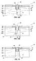
- FIG. 15is a cross-sectional side view of the exemplary substrate structure of FIG. 14 following formation of a plated dam over the solder and metal layer of a TWI to create a capped TWI, in accordance with the invention
- FIG. 16is an enlarged upper view of an exemplary bond pad and capped TWI of a substrate structure, in accordance with the invention.
- FIG. 17is a cross-sectional side view of the exemplary substrate structure of FIG. 15 during attachment of another substrate thereto by solder ball, in accordance with the invention.
- FIG. 18is a cross-sectional side view of an exemplary substrate with a capped TWI not passing through a bond pad, in accordance with another embodiment of the invention.
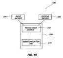
- FIG. 19is a schematic block diagram of an electronic system incorporating structures according to the present invention.
- the inventioncomprises methods for forming through vias (“TV”) or through-wafer interconnects (“TWIs”) through a substrate structures.
- viais a general term denoting a conductor passing through a substrate structure.
- through-wafer interconnectis often used more specifically where the substrate structure is a wafer of semiconductor material (e.g., a semiconductor wafer).
- substrateand “wafer” will be used interchangeably as encompassing any substrate material which may be subjected to a thinning process for reducing its thickness.
- the methods of the present inventionrelate to semiconductor devices whether in the wafer form or individualized die form that are thinnable to a final thickness.
- substraterefers not only to silicon wafers (e.g., monocrystalline silicon or polycrystalline silicon) but may also refer to silicon on insulator (“SOI”) substrates, silicon on sapphire (“SOS”) substrates, silicon on glass (“SOG”) substrates, epitaxial layers of silicon on a base semiconductor foundation, and other materials as known in the art, such as gallium arsenide, diamond, silicon-germanium, germanium, ruby, quartz, sapphire, silicon carbide and indium phosphide.
- SOIsilicon on insulator
- SOSsilicon on sapphire
- SOGsilicon on glass
- epitaxial layers of silicon on a base semiconductor foundationsuch as gallium arsenide, diamond, silicon-germanium, germanium, ruby, quartz, sapphire, silicon carbide and indium phosphide.
- the present inventionmay relate to semi-conductive or non-conductive substrates, without limitation.
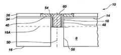
- the first surface 14(e.g., active surface) of the substrate structure 10 may be typically covered with a first oxide layer 34 , as known in the art.
- the first oxide layer 34may be a silicon oxide layer, such as a layer of silicon dioxide (SiO 2 ), phosphorus silicon glass (“PSG”), borosilicate glass (“BSG”), borophosphosilicate glass (“BPSG”), or spin-on dielectric (“SOD”).
- First oxide layer 34 on a first substrate surface 14is shown in FIG. 2 as being partially covered by a first passivation layer 36 .
- This first passivation layer 36may be typically formed from silicon dioxide, silicon nitride, silicon oxynitride, BPSG, PSG, BSG, polyimide, benzocyclobutene, mixtures thereof, or other dielectric materials as known in the art.
- the first passivation layer 36may include at least one layer of both SiO 2 and SiN (e.g., a so-called sandwich structure), as known in the art.
- the first passivation layer 36may typically have a thickness of about 0.1 ⁇ m to 10 ⁇ m.
- the first oxide layer 34 , electronic circuitry (not shown) terminating in bond pads 40 , and first passivation layer 36may be formed on the bulk substrate material 8 prior to formation of a TWI 20 according to the present invention.
- FIG. 1One method of the present invention is generally outlined in FIG. 1 and illustrated in FIGS. 2 through 16 , and relates to a substrate structure 10 which may be an exemplary multi-die semiconductor wafer residing on bulk substrate 8 .
- a substrate structure 10which may be an exemplary multi-die semiconductor wafer residing on bulk substrate 8 .
- the method outlined in FIG. 1does not explicitly show every action encompassed therein. For example, various cleaning actions are not shown, but are well-known to those of one of ordinary skill in the art.
- the present inventioncontemplates that a plurality of bond pads formed on a first surface of a substrate may be electrically joined by TWIs to a second surface thereof. Furthermore, the substrate structure or wafer may be thinned from an initial thickness to a selected final thickness. It should be understood that the particular processes, materials, or combinations thereof employed for accomplishing individual actions may vary, resulting in many embodiments. A discussion of specific preferred embodiments follows, including references to exemplary variations and additions, among others, which may be, optionally, applied to the basic methods of the present invention.
- a substrate structure 10may be provided from bulk substrate 8 having an initial thickness 12 defined between first surface 14 and second surface 16 .
- Initial thickness 12may be reduced to a selected final thickness 12 A, which may correspond to a depth to which TWIs are selected to extend.
- substrate structure 10may be thinned from first surface 14 , if desired, without limitation, if it is devoid of structures thereon which would be damaged thereby.
- the present inventioncontemplates a method for forming at least one TWI 20 (shown in FIGS. 14 and 15 ) passing from the first surface 14 to a thinned second surface 16 A of the substrate structure 10 , for electrical connection therebetween.
- the location(s) of the desired TWI(s) 20are selected or determined and preferably may be pre-programmed into process control software for automated formation of blind holes 18 in the first surface 14 .
- a TWI 20may be located so as to at least partially intersect with bond pad 40 on the first surface 14 (i.e., active surface). Accordingly, in one embodiment, it may be desirable to select a position for forming a TWI 20 which generally centers a cross-sectional area intersecting bond pad 40 with respect to a center of bond pad 40 . Put another way, a centroid of a cross-sectional area of a TWI 20 may be substantially aligned with a centroid of a cross-sectional area of a bond pad.
- a blind hole 18may be formed generally through at least a portion of bond pad 40 or may be positioned as otherwise desired.
- a plurality of blind holes 18may have openings 32 which may be typically located in an array (not shown) on the first surface 14 .
- Blind hole 18may be formed by any method which may accurately form a blind hole of a desired shape, depth 22 ( FIG. 6 ) and width 24 into bulk substrate 8 of substrate structure 10 and through any overlying structure 26 ( FIG. 2 ).
- a blind hole 18 with an opening 32may be formed by laser drilling or ablation, conventional dry etch chemistries such as a reactive ion etch, conventional wet etch chemistries, mechanical drilling, combinations thereof, or by any other process for forming recesses in a substrate structure 10 .
- a combination of processes or treatmentsmay be utilized, particularly where overlying structure 26 includes at least one of passivation materials, conductive bond pads, and a photoresist layer.
- the blind hole 18may be formed at least partially through a bond pad 40 , an underlying first oxide layer 34 , and into a portion of the bulk substrate 8 .
- blind hole 18may be formed by any of a variety of ways, the exemplary method shown in FIGS. 3 through 7 is a combination of several different methods.
- a photoresist layer 44is formed to cover the bond pads 40 and surrounding region.
- the photoresist layer 44is then patterned as shown in FIG. 4 to establish the blind hole location and size, as known in the art.
- an initial etchmay be conducted through bond pads 40 using a conventional anisotropic (dry) etch or an isotropic (wet) etch chemistry.
- an anisotropic etchmay be conducted to extend the blind hole 18 through first oxide layer 34 and into bulk substrate 8 with, for example, a Bosch type (SF 6 ,C 2 F 4 ) etch chemistry or other suitable etch chemistry.
- the blind hole 18may be further deepened by either additional etching or laser ablation to the depth 22 shown in FIG. 6 .
- the depth 22 of blind hole 18(from first surface 14 ) may be at least equal to, and preferably slightly greater than, a desired final substrate thickness 12 A and may, by way of example only, exhibit a width or diameter 24 of approximately 50 ⁇ m or less.
- a passivation layer 48may be formed upon the sidewalls 28 of the blind hole 18 which is deposited or formed (e.g., by oxidation of a portion of bulk substrate 8 ) by methods well known in the art. Such methods may include, by way of example and without limitation, physical vapor deposition (PVD), atomic layer deposition (ALD), chemical vapor deposition (CVD), low pressure chemical vapor deposition (LPCVD), rapid thermal nitridation (RTN), a spin-on-glass (SOG) process, flow coating or any other known process.
- PVDphysical vapor deposition
- ALDatomic layer deposition
- CVDchemical vapor deposition
- LPCVDlow pressure chemical vapor deposition
- RTNrapid thermal nitridation
- SOGspin-on-glass
- Passivation layer 48may be formed by oxidation of the semiconductor material surface (e.g., silicon) surface and may comprise any of a pulse deposition layer comprising aluminum-rich oxide, silicon dioxide, silicon nitride, or silicon oxynitride, a glass (i.e., borophosphosilicate glass, phosphosilicate glass, or borosilicate glass), a polymer such as ParyleneTM, benzocyclobutene (BCB) or any dielectric material having a sufficiently low dielectric constant known in the art. Accordingly, the passivation layer 48 may be, for example, silicon dioxide or other oxide, an organic coating or other electrically insulative material.
- a pulse deposition layercomprising aluminum-rich oxide, silicon dioxide, silicon nitride, or silicon oxynitride, a glass (i.e., borophosphosilicate glass, phosphosilicate glass, or borosilicate glass), a polymer such as ParyleneTM, benzocyclobutene (BC
- passivation layer 48may comprise a layer of low stress or low silicon oxide (LSO) deposited at a thickness ranging from about 0.1 ⁇ m to about 5 ⁇ m, and more generally approximately 1 to 2 ⁇ m.
- LSOlow stress or low silicon oxide
- Passivation layer 48is depicted in FIG. 8 , wherein a deposition method has also covered other surfaces of the substrate structure 10 , as well as the blind hole end 42 of blind hole 18 .
- the passivation layer 30adjoins the first oxide layer 34 to form a continuous covering within the blind hole 18 , electrically insulating the blind hole 18 from the semiconductive material of bulk substrate 8 .
- a conductive layer 54may be deposited within the blind hole 18 .
- conductive layer 54may be deposited within blind hole 18 by, for example, electroless plating, electroplating or any other suitable technique.
- a relatively thin seed layer 52may be deposited upon the passivation layer 48 , as depicted in FIG. 9 .
- This seed layer 52may be any material which enhances the adhesion of a deposited (e.g., electroless) metal thereto.
- a seed layer 52 of copper or tantalummay be subsequently plated with a metal, such as copper or nickel to form conductive layer 54 .
- the seed layer 52has a thickness of about 0.5 to 2 ⁇ m and may comprise one or both of tantalum (Ta) or copper (Cu) deposited as a pulse deposition layer (PDL) of about 1 ⁇ m thickness.
- the seed layer 52may be discontinuous.
- the seed layer 52 and underlying passivation layer 48may be removed (e.g., as by etching) from the exterior of substrate structure 10 and from bond pad surfaces 41 , as shown in FIG. 10 .
- the uppermost portion of the seed layer 52 and underlying passivation layer 48 proximate the bond pad 40may also be removed, as shown in FIG. 10 , so as to expose an inner side portion of the bond pad 40 surrounding blind hole 18 so that an electrically conductive, solder-wetting layer (e.g., conductive layer 54 as shown in FIG. 11 ) applied thereon will form electrical contact therewith.
- a conductive layer 54may be formed (e.g., electroplated or electroless plated) over the seed layer 52 within an interior of the blind hole 18 and may be solder-wetting.
- conductive layer 54may comprise copper or nickel and may exhibit a layer thickness of about 5 ⁇ m or less. Typically, a layer thickness of conductive layer 54 may be approximately 3 ⁇ m or less. Methods for metal deposition are well known in the electronics art.
- the substrate structure 10may be first cleaned and then immersed in a bath containing the electroless nickel plating solution to form a conductive layer 54 comprising nickel.
- the conductive layer 54may act as a wetting layer enabling molten solder to more effectively fill the blind hole portion of the TWI 20 .
- electroless nickel plating solutionsare known in the art, such as electroless nickel-phosphorus plating solutions or electroless nickel-boron plating solutions.
- electroless nickel plating solutionsare commercially available, such as NicPac 2.1, NicPac 2.2, and NicPac 2.3, which are available from PacTech GmbH (Berlin, Germany); and Ronamax® SMT, Duraposit® D, Niposit®, NiplateTM, which are available from Rohm & Haas Electronic Materials (Philadelphia, Pa.)
- Such electroless nickel plating solutionsmay include nickel salts such as nickel sulfate, nickel chloride, nickel bromide, nickel fluoroborate, nickel sulfonate, nickel sulfamate, and nickel aryl sulfonates, as a source of nickel ions.
- an electroless nickel solutionmay also include a reducing agent, an alkali for pH control, and complexing agents.
- nickel ionsare reduced to nickel by oxidation of the reducing agent.
- the nickel plating solutionmay be maintained at a temperature range from about 60° C. to about 100° C.
- a concentration of nickel ions in the electroless plating solution, the plating temperature, and the time of exposure (immersion time)may be selectively controlled to provide a desired thickness of conductive layer 54 on the sidewalls 28 and blind end 42 .
- a vent hole 56may be formed from the second surface 16 to the blind hole 18 .
- vent hole 56may at least partially intersect with blind hole 18 .
- vent hole 56may extend a distance 58 from the second surface 16 and into the blind end 42 and portions of layers 48 , 52 and 54 which overlie the blind end 42 .
- blind hole 18 and vent hole 56may, in combination, form an interconnected through hole extending between the first surface 14 and the second surface 16 .
- vent hole 56may intersect the blind end 42 of blind hole 18 coaxially along central axis 50 .
- vent hole 56 Amay be sized (e.g., in diameter) smaller than a cross-sectional size (e.g., a diameter) of blind hole 18 , if desired.
- the vent hole 56 Amay have any vent hole diameter 59 suitable for permitting the escape of gases without interfering with molten solder at least substantially or completely filling the blind hole 18 .
- the blind hole 18 and the vent hole 56 Amay be structured so that introducing solder into the blind hole 18 generally from the first surface 14 causes gas within the blind hole 18 to flow at least into the vent hole 56 A and toward the second surface 16 .
- a vent holemay be sized so that a surface tension of a molten solder impedes introduction thereof within vent hole while being suitably sized for permitting the escape of gases from blind hole 18 .
- FIG. 12Cshows a vent hole 56 A that is sized so that the surface tension forces of the solder 60 (note arcuate surface of solder protruding partially within vent hole 56 A) inhibits introduction of the solder 60 (when molten) into the vent hole from the blind hold 18 .
- Other factorssuch as manufacturing time for forming a plurality of vent holes 56 A, heat generated, if any, or ease in locating the vent hole 56 A in relation to the blind hole 18 may be considered in selecting a size, orientation, and structure for a vent hole.
- a vent hole 56 B(i.e., a central axis 57 thereof) may intersect the blind end 42 of blind hole 18 at an incident angle (with respect to central axis 50 ) of up to about 45 degrees (not shown).
- the vent hole diameter 59may be approximately equal to the blind hole width or diameter 24 . If the vent hole 56 is formed with a vent hole diameter 59 equal to or greater than the blind hole width or diameter 24 , the blind hole 18 will be exposed at the intersection 25 of the vent hole 56 and the blind hole 18 .
- the vent hole 56opens up the blind end 42 to ensure that solder 60 will fill blind hole 18 without forming voids. Such voids may occur when attempting to fill blind holes with solder, particularly blind holes having relatively high aspect ratios (i.e., long, slender or small diameter blind holes).
- vent hole 56Various methods may be used for forming the vent hole 56 , including laser drilling or ablation, dry etching (e.g., reactive ion etching), photochemical etching, masking and anisotropic etching, mechanical drilling, or other processes which will form openings in semiconductor (and other) substrate structure 10 . Each of these methods may be utilized to produce blind holes, through holes, or combinations thereof in substrates, as known in the art. Regardless of the method used to form the vent hole 56 , the vent hole 56 and blind hole 18 may generally require cleaning prior to at least partially filling blind hole 18 of the TWI 20 with solder 60 .
- a currently preferred method for forming a vent hole 56 of small diameter (e.g., less than about 50 ⁇ m), of high aspect ratio (e.g., greater than about 1), or combinations thereofis laser ablation.
- a 6% tetramethyl ammonium hydroxide (TMAH) in propylene glycol solutionmay be used to clean the vent hole 56 .
- solder-filling methods for the inventionmay include drag soldering, hot air solder leveling (HASL), chemical vapor deposition (CVD), physical vapor deposition (PVD), electroless deposition and electroplating, depending upon the blind hole dimensions 22 , 24 ( FIGS. 5 and 6 ).
- HSLhot air solder leveling
- CVDchemical vapor deposition
- PVDphysical vapor deposition
- electroless deposition and electroplatingdepending upon the blind hole dimensions 22 , 24 ( FIGS. 5 and 6 ).
- Suitable solder compositionsinclude, by way of example only, Sn/Pb solders, Sn/Pb/Ag solders, Sn/Pb/Sb solders, Sn/Ag solders, Sn/Sb solders, Au/Sn solders and Sn/Ag/Sb solders, Bi/Sn solders and In/Sn solders.
- Sn/Pb soldersFor blind holes 18 of small lateral dimension or width 24 , such as less than about 50 ⁇ m diameter, an improved wave soldering method may be used to solder-fill the holes with solder 60 .
- molten soldermay form a vertical (or near vertical) stream impinging on the openings 32 of the blind holes 18 to be filled.
- the substrate structure 10is held by a fixture (not shown) in a vertical, near-vertical ( ⁇ about 45°), or other orientation (e.g., inverted or substantially horizontal) to be impinged upon by molten solder 60 whereby blind holes 18 are filled.
- the methodis very effective for void-free filling of small blind holes and through holes with solder. This method is described in a co-pending Provisional Patent Application No. 60/606,798, filed Sep.
- the methodmay include actions of repositioning the substrate structure 10 in several configurations and reflowing the solder 60 to ensure complete filling of each blind hole 18 . Such a method may be very rapid and effective.
- solder-filling methodwhich may be used is to “shoot” solder balls into the blind hole 18 and then melted to flow. The actions may be repeated as necessary to completely fill the hole.
- One source of equipment for effecting such a methodis available from Pac Tech GmbH of Nauen, Germany.
- Solder pastehas also been used to fill blind holes in the prior art. However, with small diameter blind holes 18 , having a diameter ⁇ about 50 ⁇ m, the use of solder paste may not be generally effective, because its high concentration of flux may cause voids in the TWI 20 .
- Evaporation and electroplating of solder into blind hole 18are also contemplated as deposition methods suitable for filling blind holes 18 . Equipment for performing such methods is available from Silex Microsystems of Jarfalla, Sweden. All of the foregoing examples of solder deposition methods are to be taken as nonlimiting of the scope of the present invention, as other deposition methods and apparatus are also suitable.
- a portion of bulk substrate material 8may be removed (i.e., thinning) into the second surface 16 to a final second surface 16 A at which the desired substrate thickness 12 A (see FIG. 2 ) may be achieved.
- bulk substrate material 8may be removed by an abrasive technique such as back grinding or chemical mechanical planarization (CMP), or as otherwise known in the art.
- CMPchemical mechanical planarization
- passivation layer 48 , seed layer 52 , and conductive layer 54 and solder 60may be planarized to exhibit surfaces generally coplanar with the final second surface 16 A.
- a substrate structure 10 having an initial thickness of about 725 ⁇ mmay be thinned to a final typical thickness of about 250 ⁇ m to 150 ⁇ m or less.
- the planarization or thinning actionmay be one of back grinding or CMP, by other abrasive techniques, or by wet etching, such methods being well established in the art.
- the conductive layer 54e.g., copper or nickel
- the conductive layer 54may be configured to taper outwardly near the first surface 14 in order to abut the bond pad 40 for electrical contact therewith.
- each of the passivation layer 48 , seed layer 52 , and conductive layer 54may be generally parallel to central axis 50 , after thinning (e.g., exposure to CMP or abrasion) and may exhibit substantially coplanar end surfaces.
- a solder dam or cap 62may then be applied to one or both ends of the TWI 20 .
- Such a configurationmay effectively hold or maintain the solder 60 within the TWI 20 .
- the solder dam or cap 62may be formed by electroless plating of a layer of metal across the exposed surface of the solder 60 and conductive layer 54 .
- a solder dam 62may comprise at least one of nickel, copper, rhenium, and gold.
- solder dam 62must have a glass transition temperature ⁇ 2 greater than the glass transition temperature ⁇ 1 of the solder or must be otherwise formulated and configured so that molten solder will not escape from the TWI 20 during high temperature excursions.
- the glass transition temperature vi of one commonly employed Pd-free solderis about 217° C.
- solder dam 62may comprise nickel, which exhibits a relatively higher glass transition temperature of about 1455° C.
- nickelmay be advantageous because it is readily applied by electroless plating to cohere to the cylindrical plated conductive layer 54 .
- the solder dam 62may prevent removal (e.g., drainage, etc.) of solder from the TWI 20 due to melting of solder 60 .
- Nickelhas additional advantages over some other metals.
- coppermay form brittle intermetallics with solder, and both rhenium and gold may form intermetallics with solder which result in poor adhesion of the dam 62 to the TWI 20 .
- the dam 62may serve as a base for solder attachment of solder ball 70 .
- a solder ball 70(or array or combination of solder balls or solder material) may be initially attached to at least one of the attach pads 72 of the second substrate 68 and solder dam 62 ; then, the solder ball 70 may then be attached (by reflowing or other suitable heating process) to the other of the exposed surface 66 of a solder dam 62 and the attach pads of second substrate 68 with the solder ball 70 .
- a nickel dam or cap 62 having an oxidized surface 66may be readily cleanable by solder flux applied thereto, or other cleaning processes as known in the art, for providing a wettable surface for solder attachment.
- a layer of goldmay be formed on at least a portion of solder dam 62 for facilitating wetting thereof (as by molten solder) or for preventing oxidation thereof.
- dam 62may serve as a barrier to prevent undesirable cross-contamination between dissimilar materials placed on either side thereof.
- the material of solder ball 70may differ from that of solder 60 within an underlying TWI 20 .
- solder 60may comprise an Au/Sn solder
- solder ball 70placed on and bonded to dam 62 by reflow, may comprise a Pb/Sn solder.
- the glass transition temperature ⁇ 2 of the material of dam 62will, of course, be greater than the glass transition temperature ⁇ 1 of solder 60 as well as the glass transition temperature ⁇ 3 of solder ball 70 in order to maintain the integrity of the barrier.
- the respective physical, thermal and electrical characteristics of each different solder materialmay be readily maintained by dam 62 .
- a photolithographic damascene processmay be used to electrically connect a dam or cap 62 to a surrounding bond pad 40 .
- a recessmay be formed by etching or laser ablation between the dam 62 and bond pad 40 , and filled with a conductor by, for example CVD or other deposition method.
- a TWI 20 in a substrate structure 10 without bond pads 40has a surrounding passivation layer 48 which fully isolates the TWI 20 from the bulk substrate material 8 .
- Dams 62may comprise nickel, which has been electroless plated across the solder 60 and conductive layer 54 .
- the methods of the inventionenable avoidance of the use of wire bonding.
- the inventionenables assembly of stacked dice and multi-chip modules (MCM) at high speed and accuracy while reducing the occurrence of defects.
- MCMmulti-chip modules
- FIG. 19shows a schematic block diagram of system 230 incorporating at least one semiconductor die 210 including structures according to the present invention.
- Semiconductor die 210may be included in a computing device 220 , such as a hand-held computing device, a computer, or another electronic device.
- the computing device 220may include a processor device 232 , such as a central processing unit or other logic device operably coupled thereto.
- Semiconductor die 210may be fabricated from a semiconductor wafer including at least one TWI according to the present invention as described above.
- processor device 232may also be coupled with one or more appropriate input devices 234 (e.g., mouse, push-button, touch screen, communication interface, hard drive, etc.) and one or more output devices 236 (e.g., a display, printer, communication interface, hard drive, etc.) within system 230 .
- the semiconductor die 210may be utilized in various computing environments, systems, and devices, such as, for example, cell phones, personal data assistants (PDAs), and other similar electronic devices.
- PDAspersonal data assistants
Landscapes
- Engineering & Computer Science (AREA)
- Computer Hardware Design (AREA)
- Microelectronics & Electronic Packaging (AREA)
- Power Engineering (AREA)
- Physics & Mathematics (AREA)
- Condensed Matter Physics & Semiconductors (AREA)
- General Physics & Mathematics (AREA)
- Manufacturing & Machinery (AREA)
- Internal Circuitry In Semiconductor Integrated Circuit Devices (AREA)
Abstract
Description
- 1. Field of the Invention
- The present invention relates to semiconductor devices and fabrication methods therefor. More particularly, the invention pertains to methods for forming conductive vias in a substrate such as a semiconductor wafer or other substrate, and resulting structures.
- 2. Background of Related Art
- Semiconductor devices that have integrated circuits are produced by fabricating a large plurality of identical circuit patterns on a semiconductor wafer or other bulk substrates of semiconductor material, wherein each circuit pattern defines a die. A plethora of conventional processes is typically used, including for example, doping, photolithography, layering, etching, laser ablation, metallization, oxidation, layer removal, wafer thinning/planarization, die separation and packaging. Inasmuch as the major goals of semiconductor manufacturers generally typify increased performance and lower cost, considerations such as device density (with concomitant increased circuit speed and reduced power requirements) and enhanced reliability have taken a high priority. In addition, it may be increasingly important that repetitive operations be performed on an entire wafer prior to die separation (singulation), to speed production, reduce production costs, and increase semiconductor device uniformity and reliability and, ultimately, yield.
- One way to increase the density of semiconductor devices in a semiconductor assembly is to stack semiconductor dice one upon another. The stacked semiconductor dice may be interconnected by forming conductive vias in through holes in one or more of the semiconductor dice. An interior of each of the vias may be coated with an electrical isolation material followed by an electrically conductive material to electrically connect the vias to integrated circuitry fabricated on an active surface of the semiconductor die and to form a plurality of hollow through-hole vias. Thus, the vias may provide a conductive pathway from the active surface of a semiconductor die to its back surface, enabling interconnection of vias on the back surface, the active surface, or both surfaces of the semiconductor die to external electrical contacts of another semiconductor die or to a carrier substrate. Through holes are typically formed by etching, laser ablation, or a combination thereof. In an etching method, photolithographic patterning of a photoresist is used to define the via locations, followed by wet (chemical) or dry (reactive ion) etching. Laser drilling has been used to form vias by ablating semiconductor material to form through holes extending through the entire thickness of a semiconductor die. The laser-drilled via may then be etched to clean slag from the via and smooth its walls.
- Various conductive structures on a die or wafer may be interconnected by a conductive via and further through at least one of bond pads, component leads, metal wires, metal layers, and annular rings. Bond pads on semiconductor dice are typically formed from tungsten, aluminum, copper, or aluminum-copper alloys ranging from 1.5 to 1.0% or less copper. When formed of aluminum, the bond pads may be plated with nickel to deter oxidation and provide a solder-wettable surface. However, a layer of oxide may also form upon nickel, though not as rapidly as aluminum. Such a layer of nickel oxide may present a problem with adhesion or wetting of a molten metal (e.g., solder) thereto.
- One of the problems encountered in the use of high density ball grid arrays (BGA), column grid arrays (CGA), or chip scale packaging (CSP) may occur when a through-wafer interconnect (TWI) of a substrate is connected to another substrate such as an electronic module or circuit board. Particularly, when the solder deposited on a bond pad associated with a hollow conductive via and is heated to a reflow temperature, molten solder may be wicked into the hollow through hole, depleting the ball of sufficient solder to complete the conductive connection.
- U.S. Pat. No. 5,275,330 to Isaacs et al. describes a method for improving the connection of hollow through-hole vias in a printed circuit board (PCB) to an electronic module. As shown in this reference, each via is filled step-wise until completely filled with solder, prior to placement and attachment of solder balls of a module. However, multiple pass solder-plugging steps are required and assembly yield may be lower than desired. This method may sometimes result in other problems, including molten/softened solder drainage from the via by gravity or other influences and replacement by solder drawn from the solder ball attachment, compromising the solder ball electrical connection.
- As shown in U.S. Pat. No. 6,076,726 to Hoffmeyer et al., it is proposed to plate the cylindrical via with a metal, such as nickel, which may not be wetted effectively by the reflowing of a lead-tin eutectic solder while using fluxes that allow effective wetting to copper. The bond pad of the via is copper plated to effect good wetting to a solder ball. The goal of the reference is to form a hollow (cylindrical) via which is not wettable for solder adhesion, while allowing the bond pad to be wetted by solder.
- As described in U.S. Pat. No. 5,734,560 to Kamperman et al., hollow plated through holes in a multi-layer circuit board are capped with a multi-layer cap to prevent the flow of solder into the through holes. The caps comprise a conductive layer attached to one or more insulating layers. The caps are configured in a sheet which may be attached over the field of through holes. However, as an impediment to implementation of such a configuration, cap locations on the sheet must be precisely positioned so as to be aligned with respective through holes.
- In U.S. Pat. No. 4,383,363 to Hayakawa et al., a solder paste is used to interconnect the conductive planes on either of a printed circuit board through a via hole. The via hole is not plated and the solder paste is not reflowed. Conductive layers deposited on the substrate and over the via entrap the solder paste within the via hole. Because the solder paste is not reflowed, electrical continuity is established through particle-to-particle contact, which is not always reliable.
- There are fundamental differences in forming vias in a circuit board and forming vias in a semiconductor wafer which contains many discrete microchip circuits. While a circuit board is typically manufactured at a desired final thickness, semiconductive materials such as silicon and the like are fragile materials subject to easy fracture. Thus, in contrast to circuit board fabrication, fabrication of electronic devices on an entire semiconductor wafer is typically conducted before the wafer is thinned by a chemical mechanical process (CMP) or back grinding to a desired final thickness. None of the above referenced patents refer to the formation of a conductive via or TWI in a semiconductor wafer such as comprising a plurality of integrated circuits or the like.
- In light of efforts to overcome the disadvantages of the prior art, it may be appreciated that it would be advantageous to develop improved methods for forming TWIs through a semiconductor wafer.
- The present invention comprises methods for making through-wafer interconnects in substrates such as semiconductor wafers and other substrates. The methods include the formation of a conductive through wafer interconnect, or TWI, having a dam structure at one or both ends. The one or more dam structures may be configured for preventing leakage or loss of solder from the via or TWI during high temperature excursions such as those which typically occur during fabrication, testing and packaging. The one or more dam structures may also provide a convenient base for the attachment of solder balls and the like. Thus, the invention may be useful for enabling column grid array (CGA), ball grid array (BGA) and other types of interconnection between stacked dice or stacked circuit boards, and/or in die-to-circuit board attachments. The present invention may also be useful for simply connecting active area bond pads to back-side conductors. Interconnects so formed may be fabricated in the wafer stage of manufacture, utilizing conventional wafer thinning techniques. At least one semiconductor die including a TWI and having at least one dam structure is encompassed by the present invention, as well as systems incorporating same.
- One embodiment of a method of the present invention is generally described, infra, by the formation of at least one TWI in a substrate such as a semiconductor wafer in an intermediate stage of manufacture. Thus, at least one TWI may be formed following the creation of multiple identical integrated circuits (IC), including bond pads, on the active surface of the wafer. However, the methods may be utilized to form at least one TWI at any stage prior to the creation of multiple identical integrated circuits (IC) and bond pads on the active surface of the wafer. The methods of the invention may also be used to form at least one TWI in substrates without passing through a bond pad. The invention also includes electronic apparatuses and systems having at least one semiconductor die including at least one through-wafer interconnect comprising at least one dam structure.
- In accordance with the invention, a plurality of TWIs may be formed in a substrate (e.g., a semiconductor wafer). Particularly, locations of a plurality of through-wafer interconnects may be selected for forming at least partially into the substrate. Further, a plurality of blind holes may be formed through any overlying structure (oxide, bond pads, etc.) into the substrate wherein a depth of each of the plurality of blind holes extends into the substrate at least to a final desired thickness thereof. Additionally, optionally, a passivation layer may be desirably applied upon the sidewalls and blind ends of the blind holes and a metal-wettable layer may be applied over the passivation layer within the blind holes. A plurality of vent holes may be formed from the opposite surface into which the plurality of blind holes are formed and may at least partially intersect the blind holes and form through holes. Also, molten solder may be deposited within the metal-wettable layer (blind hole portion) of the through holes and solidified. Put another way, an intermediate structure for fabricating a plurality of semiconductor devices is encompassed by the present invention. Particularly, such a semiconductor wafer may include a first surface and a second surface and a plurality of recesses formed into the substrate from the first surface. Further, the semiconductor wafer may include a plurality of vent holes extending from the second surface, wherein each of the plurality of vent holes at least partially intersects with a respective recess of the plurality of recesses and wherein each of the plurality of recesses is substantially filled with solder and each of the plurality of vent holes is substantially devoid of solder. The substrate may be thinned to a desired final substrate thickness as by back grinding, removing at least the vent holes and a portion of the substrate material underlying the recesses and forming solder-filled, through-wafer interconnects.
- In a further aspect of the invention, at least one dam structure may be formed over at least one end of a via or TWI by electroless plating of a metal such as nickel or copper over at least one solder-filled metal end of the through holes, forming at least one cap or dam structure which may prevent drainage of solder therefrom during elevated temperatures at which solder melts. The exposed surface of the at least one dam structure may be photoresist etched to form a solder-retaining pattern to which a connector (e.g., solder ball) may be securely attached. The at least one dam structure may also be used to keep dissimilar materials located on either side thereof separated, and eliminate cross-contamination concerns. Accordingly, at least one semiconductor die or semiconductor die precursor structure (e.g., a semiconductor wafer) may be formed. Further, such a semiconductor die may be incorporated within a semiconductor device or system. For example, the methods of the invention may be particularly advantageous in the production of die-stacked devices, such as stacked DRAMs, SRAMs, PCRAMs, MRAMs, CAMs, flash memory devices, imagers, and the like. The method is also useful for simply connecting conductors on opposing surfaces of a thinnable substrate.
- The methods of the invention offer substantial advantages over the prior art. The methods may solve the problems of solder leakage and may reduce an occurrence of unwanted voids in the solder. Reflow induced solder connection of a device (or wafer of devices) to another adjacent substrate or circuit board, etc. may be readily conducted without fear of solder loss at the elevated temperatures. The methods may be advantageous for enabling the production of high-density TWI arrays. Furthermore, all of the actions of the methods of the present invention may be conducted at a semiconductor wafer stage, whereby each action of the methods may simultaneously encompass all of the individual devices on the semiconductor wafer.
- Other features and advantages of the present invention will become apparent to those of skill in the art through consideration of the ensuing detailed description, the accompanying drawings, and the appended claims. The drawings are idealized representations for better illustration of the methods of the invention, and various elements are not necessarily shown to scale.
- In the drawings, which depict exemplary embodiments of various features of the present invention:
FIG. 1 is a flowchart showing one embodiment of a general method for producing a through-wafer interconnect (TWI) in a substrate in accordance with the invention;FIG. 2 is a cross-sectional side view of a portion of an exemplary substrate structure in which a TWI is to be formed in accordance with the invention;FIG. 3 is a cross-sectional side view of the exemplary substrate structure ofFIG. 2 following application of a photoresist layer in accordance with one embodiment of the invention;FIG. 4 is a cross-sectional side view of the exemplary substrate structure ofFIG. 3 following etching a hole pattern through the photoresist layer, in accordance with one embodiment of the invention;FIG. 5 is a cross-sectional side view of the exemplary substrate structure ofFIG. 4 following formation of a blind hole through a bond pad and oxide layer, in accordance with an embodiment of the invention;FIG. 6 is a cross-sectional side view of the exemplary substrate structure ofFIG. 5 following extension of the blind hole into the bulk substrate material, in accordance with one embodiment of the invention;FIG. 7 is a cross-sectional side view of the exemplary substrate structure ofFIG. 6 following stripping of a photoresist layer from the structure, in accordance with one embodiment of the invention;FIG. 8 is a cross-sectional side view of the exemplary substrate structure ofFIG. 7 following application of a passivation layer in the blind hole, in accordance with the invention;FIG. 9 is a cross-sectional side view of the exemplary substrate structure ofFIG. 8 following application of a metallic seed layer over the passivation layer, in accordance with an embodiment of the invention;FIG. 10 is a cross-sectional side view of the exemplary substrate structure ofFIG. 9 following removal of extraneous passivation material external to the blind hole, in accordance with the invention;FIG. 11 is a cross-sectional side view of the exemplary substrate structure ofFIG. 10 following plating of a solder-wetting metal over the passivation material within the blind hole, in accordance with the invention;FIG. 12A is a cross-sectional side view of the exemplary substrate structure ofFIG. 11 following formation of a vent hole from the back side of the substrate structure to intersect the blind hole and create a through hole, in accordance with the invention;FIG. 12B is a cross-sectional side view of another exemplary substrate structure ofFIG. 11 following formation of a vent hole from the back side of the substrate structure to intersect the blind hole and create a through hole, in accordance with the invention;FIG. 12C is a cross-sectional side view of the vent hole configuration shown inFIG. 12B , including solder deposited within the blind hole;FIG. 12D is a cross-sectional side view of a further exemplary substrate structure ofFIG. 11 following formation of a vent hole from the back side of the substrate structure to intersect the blind hole and create a through hole, in accordance with the invention;FIG. 13 is a cross-sectional side view of the exemplary substrate structure ofFIG. 12 following solder fill into the metal plated portion of the through hole, in accordance with the invention;FIG. 14 is a cross-sectional side view of the exemplary substrate structure ofFIG. 13 following thinning of the back side to a desired thickness, in accordance with the invention;FIG. 15 is a cross-sectional side view of the exemplary substrate structure ofFIG. 14 following formation of a plated dam over the solder and metal layer of a TWI to create a capped TWI, in accordance with the invention;FIG. 16 is an enlarged upper view of an exemplary bond pad and capped TWI of a substrate structure, in accordance with the invention;FIG. 17 is a cross-sectional side view of the exemplary substrate structure ofFIG. 15 during attachment of another substrate thereto by solder ball, in accordance with the invention;FIG. 18 is a cross-sectional side view of an exemplary substrate with a capped TWI not passing through a bond pad, in accordance with another embodiment of the invention; andFIG. 19 is a schematic block diagram of an electronic system incorporating structures according to the present invention.- The invention comprises methods for forming through vias (“TV”) or through-wafer interconnects (“TWIs”) through a substrate structures. The term “via” is a general term denoting a conductor passing through a substrate structure. The term “through-wafer interconnect” is often used more specifically where the substrate structure is a wafer of semiconductor material (e.g., a semiconductor wafer). In this application, the terms “substrate” and “wafer” will be used interchangeably as encompassing any substrate material which may be subjected to a thinning process for reducing its thickness. Thus, the methods of the present invention relate to semiconductor devices whether in the wafer form or individualized die form that are thinnable to a final thickness. Accordingly, the term “substrate” refers not only to silicon wafers (e.g., monocrystalline silicon or polycrystalline silicon) but may also refer to silicon on insulator (“SOI”) substrates, silicon on sapphire (“SOS”) substrates, silicon on glass (“SOG”) substrates, epitaxial layers of silicon on a base semiconductor foundation, and other materials as known in the art, such as gallium arsenide, diamond, silicon-germanium, germanium, ruby, quartz, sapphire, silicon carbide and indium phosphide. Thus, the present invention may relate to semi-conductive or non-conductive substrates, without limitation.
- It will be understood that methods for wafer fabrication and packaging which precede and follow the methods described herein are generally known to those of ordinary skill in the art and, thus, are not described apart from the context of the invention. Also, while the drawings show a single TWI20 (see, for example,
FIGS. 15 through 17 ) for clarity and simplicity it is understood that the present invention contemplates any number (e.g., a plurality) of TWIs may be formed within a substrate. Thus, hundreds or even thousands of TWIs may be formed within a single wafer or substrate (e.g., a semiconductor wafer). - For example, as shown in
FIG. 2 , where thesubstrate structure 10 is an unseparated plurality of semiconductor devices in wafer form, the first surface14 (e.g., active surface) of thesubstrate structure 10 may be typically covered with afirst oxide layer 34, as known in the art. Thefirst oxide layer 34 may be a silicon oxide layer, such as a layer of silicon dioxide (SiO2), phosphorus silicon glass (“PSG”), borosilicate glass (“BSG”), borophosphosilicate glass (“BPSG”), or spin-on dielectric (“SOD”). First oxide layer 34 on afirst substrate surface 14 is shown inFIG. 2 as being partially covered by afirst passivation layer 36. Thisfirst passivation layer 36 may be typically formed from silicon dioxide, silicon nitride, silicon oxynitride, BPSG, PSG, BSG, polyimide, benzocyclobutene, mixtures thereof, or other dielectric materials as known in the art. For example, thefirst passivation layer 36 may include at least one layer of both SiO2and SiN (e.g., a so-called sandwich structure), as known in the art. Also, thefirst passivation layer 36 may typically have a thickness of about 0.1 μm to 10 μm. Further, thefirst oxide layer 34, electronic circuitry (not shown) terminating inbond pads 40, andfirst passivation layer 36 may be formed on thebulk substrate material 8 prior to formation of aTWI 20 according to the present invention.- One method of the present invention is generally outlined in
FIG. 1 and illustrated inFIGS. 2 through 16 , and relates to asubstrate structure 10 which may be an exemplary multi-die semiconductor wafer residing onbulk substrate 8. However, the method outlined inFIG. 1 does not explicitly show every action encompassed therein. For example, various cleaning actions are not shown, but are well-known to those of one of ordinary skill in the art. - Generally, the present invention contemplates that a plurality of bond pads formed on a first surface of a substrate may be electrically joined by TWIs to a second surface thereof. Furthermore, the substrate structure or wafer may be thinned from an initial thickness to a selected final thickness. It should be understood that the particular processes, materials, or combinations thereof employed for accomplishing individual actions may vary, resulting in many embodiments. A discussion of specific preferred embodiments follows, including references to exemplary variations and additions, among others, which may be, optionally, applied to the basic methods of the present invention.
- As indicated in
FIGS. 2 and 3 , asubstrate structure 10 may be provided frombulk substrate 8 having aninitial thickness 12 defined betweenfirst surface 14 andsecond surface 16.Initial thickness 12 may be reduced to a selectedfinal thickness 12A, which may correspond to a depth to which TWIs are selected to extend. Of course, optionally,substrate structure 10 may be thinned fromfirst surface 14, if desired, without limitation, if it is devoid of structures thereon which would be damaged thereby. The present invention contemplates a method for forming at least one TWI20 (shown inFIGS. 14 and 15 ) passing from thefirst surface 14 to a thinnedsecond surface 16A of thesubstrate structure 10, for electrical connection therebetween. The location(s) of the desired TWI(s)20 are selected or determined and preferably may be pre-programmed into process control software for automated formation ofblind holes 18 in thefirst surface 14. In the example depicted in the figures, aTWI 20 may be located so as to at least partially intersect withbond pad 40 on the first surface14 (i.e., active surface). Accordingly, in one embodiment, it may be desirable to select a position for forming aTWI 20 which generally centers a cross-sectional area intersectingbond pad 40 with respect to a center ofbond pad 40. Put another way, a centroid of a cross-sectional area of aTWI 20 may be substantially aligned with a centroid of a cross-sectional area of a bond pad. - Referring to
FIG. 5 and as mentioned hereinabove, ablind hole 18 may be formed generally through at least a portion ofbond pad 40 or may be positioned as otherwise desired. For example, a plurality ofblind holes 18 may haveopenings 32 which may be typically located in an array (not shown) on thefirst surface 14.Blind hole 18 may be formed by any method which may accurately form a blind hole of a desired shape, depth22 (FIG. 6 ) andwidth 24 intobulk substrate 8 ofsubstrate structure 10 and through any overlying structure26 (FIG. 2 ). Thus, ablind hole 18 with anopening 32 may be formed by laser drilling or ablation, conventional dry etch chemistries such as a reactive ion etch, conventional wet etch chemistries, mechanical drilling, combinations thereof, or by any other process for forming recesses in asubstrate structure 10. A combination of processes or treatments may be utilized, particularly whereoverlying structure 26 includes at least one of passivation materials, conductive bond pads, and a photoresist layer. In the illustrated example shown inFIGS. 3 through 5 , theblind hole 18 may be formed at least partially through abond pad 40, an underlyingfirst oxide layer 34, and into a portion of thebulk substrate 8. - Although
blind hole 18 may be formed by any of a variety of ways, the exemplary method shown inFIGS. 3 through 7 is a combination of several different methods. As shown inFIG. 3 , aphotoresist layer 44 is formed to cover thebond pads 40 and surrounding region. Thephotoresist layer 44 is then patterned as shown inFIG. 4 to establish the blind hole location and size, as known in the art. As depicted inFIG. 5 , an initial etch may be conducted throughbond pads 40 using a conventional anisotropic (dry) etch or an isotropic (wet) etch chemistry. Then, an anisotropic etch may be conducted to extend theblind hole 18 throughfirst oxide layer 34 and intobulk substrate 8 with, for example, a Bosch type (SF6,C2F4) etch chemistry or other suitable etch chemistry. Theblind hole 18 may be further deepened by either additional etching or laser ablation to thedepth 22 shown inFIG. 6 . Thedepth 22 of blind hole18 (from first surface14) may be at least equal to, and preferably slightly greater than, a desiredfinal substrate thickness 12A and may, by way of example only, exhibit a width ordiameter 24 of approximately 50 μm or less. - As shown in
FIG. 8 , in order to electrically isolate the TWI20 (FIGS. 15-17 ) from thebulk substrate 8, apassivation layer 48 may be formed upon thesidewalls 28 of theblind hole 18 which is deposited or formed (e.g., by oxidation of a portion of bulk substrate8) by methods well known in the art. Such methods may include, by way of example and without limitation, physical vapor deposition (PVD), atomic layer deposition (ALD), chemical vapor deposition (CVD), low pressure chemical vapor deposition (LPCVD), rapid thermal nitridation (RTN), a spin-on-glass (SOG) process, flow coating or any other known process.Passivation layer 48 may be formed by oxidation of the semiconductor material surface (e.g., silicon) surface and may comprise any of a pulse deposition layer comprising aluminum-rich oxide, silicon dioxide, silicon nitride, or silicon oxynitride, a glass (i.e., borophosphosilicate glass, phosphosilicate glass, or borosilicate glass), a polymer such as Parylene™, benzocyclobutene (BCB) or any dielectric material having a sufficiently low dielectric constant known in the art. Accordingly, thepassivation layer 48 may be, for example, silicon dioxide or other oxide, an organic coating or other electrically insulative material. For example,passivation layer 48 may comprise a layer of low stress or low silicon oxide (LSO) deposited at a thickness ranging from about 0.1 μm to about 5 μm, and more generally approximately 1 to 2 μm.Passivation layer 48 is depicted inFIG. 8 , wherein a deposition method has also covered other surfaces of thesubstrate structure 10, as well as theblind hole end 42 ofblind hole 18. As shown, the passivation layer30 adjoins thefirst oxide layer 34 to form a continuous covering within theblind hole 18, electrically insulating theblind hole 18 from the semiconductive material ofbulk substrate 8. - As shown in
FIG. 11 , aconductive layer 54 may be deposited within theblind hole 18. For example,conductive layer 54 may be deposited withinblind hole 18 by, for example, electroless plating, electroplating or any other suitable technique. In order to enhance coverage ofconductive layer 54, especially in verysmall TWIs 20, a relativelythin seed layer 52, as known in the art, may be deposited upon thepassivation layer 48, as depicted inFIG. 9 . Thisseed layer 52 may be any material which enhances the adhesion of a deposited (e.g., electroless) metal thereto. For example, aseed layer 52 of copper or tantalum may be subsequently plated with a metal, such as copper or nickel to formconductive layer 54. Other metals or metal salts may be utilized as seed materials as known in the art. Typically, theseed layer 52 has a thickness of about 0.5 to 2 μm and may comprise one or both of tantalum (Ta) or copper (Cu) deposited as a pulse deposition layer (PDL) of about 1 μm thickness. Theseed layer 52 may be discontinuous. - Following deposition of the
seed layer 52, theseed layer 52 andunderlying passivation layer 48 may be removed (e.g., as by etching) from the exterior ofsubstrate structure 10 and from bond pad surfaces41, as shown inFIG. 10 . Where it is desired to electrically connect theTWI 20 to thebond pad 40, the uppermost portion of theseed layer 52 andunderlying passivation layer 48 proximate thebond pad 40 may also be removed, as shown inFIG. 10 , so as to expose an inner side portion of thebond pad 40 surroundingblind hole 18 so that an electrically conductive, solder-wetting layer (e.g.,conductive layer 54 as shown inFIG. 11 ) applied thereon will form electrical contact therewith. - Thus, as depicted in
FIG. 11 , aconductive layer 54 may be formed (e.g., electroplated or electroless plated) over theseed layer 52 within an interior of theblind hole 18 and may be solder-wetting. For example,conductive layer 54 may comprise copper or nickel and may exhibit a layer thickness of about 5 μm or less. Typically, a layer thickness ofconductive layer 54 may be approximately 3 μm or less. Methods for metal deposition are well known in the electronics art. In an exemplary electroless plating of nickel over aseed layer 52 for formingconductive layer 54, thesubstrate structure 10 may be first cleaned and then immersed in a bath containing the electroless nickel plating solution to form aconductive layer 54 comprising nickel. Thus, theconductive layer 54 may act as a wetting layer enabling molten solder to more effectively fill the blind hole portion of theTWI 20. A wide variety of electroless nickel plating solutions are known in the art, such as electroless nickel-phosphorus plating solutions or electroless nickel-boron plating solutions. - For example, electroless nickel plating solutions are commercially available, such as NicPac 2.1, NicPac 2.2, and NicPac 2.3, which are available from PacTech GmbH (Berlin, Germany); and Ronamax® SMT, Duraposit® D, Niposit®, Niplate™, which are available from Rohm & Haas Electronic Materials (Philadelphia, Pa.) Such electroless nickel plating solutions may include nickel salts such as nickel sulfate, nickel chloride, nickel bromide, nickel fluoroborate, nickel sulfonate, nickel sulfamate, and nickel aryl sulfonates, as a source of nickel ions. Also, as known in the art, an electroless nickel solution may also include a reducing agent, an alkali for pH control, and complexing agents. During electroless plating, nickel ions are reduced to nickel by oxidation of the reducing agent. The nickel plating solution may be maintained at a temperature range from about 60° C. to about 100° C. A concentration of nickel ions in the electroless plating solution, the plating temperature, and the time of exposure (immersion time) may be selectively controlled to provide a desired thickness of
conductive layer 54 on thesidewalls 28 andblind end 42. - As shown in
FIG. 12A , avent hole 56 may be formed from thesecond surface 16 to theblind hole 18. Generally, venthole 56 may at least partially intersect withblind hole 18. As shown inFIG. 12A , venthole 56 may extend adistance 58 from thesecond surface 16 and into theblind end 42 and portions oflayers blind end 42. Thus,blind hole 18 and venthole 56 may, in combination, form an interconnected through hole extending between thefirst surface 14 and thesecond surface 16. - Optionally, the
vent hole 56 may intersect theblind end 42 ofblind hole 18 coaxially alongcentral axis 50. Also, optionally, as shown inFIG. 12B , venthole 56A may be sized (e.g., in diameter) smaller than a cross-sectional size (e.g., a diameter) ofblind hole 18, if desired. Generally, thevent hole 56A may have anyvent hole diameter 59 suitable for permitting the escape of gases without interfering with molten solder at least substantially or completely filling theblind hole 18. Put another way, theblind hole 18 and thevent hole 56A may be structured so that introducing solder into theblind hole 18 generally from thefirst surface 14 causes gas within theblind hole 18 to flow at least into thevent hole 56A and toward thesecond surface 16. - Further, a vent hole may be sized so that a surface tension of a molten solder impedes introduction thereof within vent hole while being suitably sized for permitting the escape of gases from
blind hole 18. Particularly,FIG. 12C shows avent hole 56A that is sized so that the surface tension forces of the solder60 (note arcuate surface of solder protruding partially withinvent hole 56A) inhibits introduction of the solder60 (when molten) into the vent hole from theblind hold 18. Other factors such as manufacturing time for forming a plurality ofvent holes 56A, heat generated, if any, or ease in locating thevent hole 56A in relation to theblind hole 18 may be considered in selecting a size, orientation, and structure for a vent hole. In a further alternative, as shown inFIG. 12D , avent hole 56B (i.e., acentral axis 57 thereof) may intersect theblind end 42 ofblind hole 18 at an incident angle (with respect to central axis50) of up to about 45 degrees (not shown). - Alternatively, as shown in
FIGS. 12A and 13 , thevent hole diameter 59 may be approximately equal to the blind hole width ordiameter 24. If thevent hole 56 is formed with avent hole diameter 59 equal to or greater than the blind hole width ordiameter 24, theblind hole 18 will be exposed at theintersection 25 of thevent hole 56 and theblind hole 18. Thevent hole 56 opens up theblind end 42 to ensure thatsolder 60 will fillblind hole 18 without forming voids. Such voids may occur when attempting to fill blind holes with solder, particularly blind holes having relatively high aspect ratios (i.e., long, slender or small diameter blind holes). - Various methods may be used for forming the
vent hole 56, including laser drilling or ablation, dry etching (e.g., reactive ion etching), photochemical etching, masking and anisotropic etching, mechanical drilling, or other processes which will form openings in semiconductor (and other)substrate structure 10. Each of these methods may be utilized to produce blind holes, through holes, or combinations thereof in substrates, as known in the art. Regardless of the method used to form thevent hole 56, thevent hole 56 andblind hole 18 may generally require cleaning prior to at least partially fillingblind hole 18 of theTWI 20 withsolder 60. A currently preferred method for forming avent hole 56 of small diameter (e.g., less than about 50 μm), of high aspect ratio (e.g., greater than about 1), or combinations thereof is laser ablation. In such an instance, a 6% tetramethyl ammonium hydroxide (TMAH) in propylene glycol solution may be used to clean thevent hole 56. - Turning now to
FIG. 13 , filling of the layeredblind hole 18 withsolder 60 is illustrated. Various solder compositions as well as methods of solder filling may be utilized, but some methods may be limited to holes of larger diameter or lower aspect ratio. Thus, useful solder-filling methods for the invention may include drag soldering, hot air solder leveling (HASL), chemical vapor deposition (CVD), physical vapor deposition (PVD), electroless deposition and electroplating, depending upon theblind hole dimensions 22,24 (FIGS. 5 and 6 ). Suitable solder compositions include, by way of example only, Sn/Pb solders, Sn/Pb/Ag solders, Sn/Pb/Sb solders, Sn/Ag solders, Sn/Sb solders, Au/Sn solders and Sn/Ag/Sb solders, Bi/Sn solders and In/Sn solders. Forblind holes 18 of small lateral dimension orwidth 24, such as less than about 50 μm diameter, an improved wave soldering method may be used to solder-fill the holes withsolder 60. - According to an improved wave soldering method, molten solder may form a vertical (or near vertical) stream impinging on the
openings 32 of theblind holes 18 to be filled. Thesubstrate structure 10 is held by a fixture (not shown) in a vertical, near-vertical (±about 45°), or other orientation (e.g., inverted or substantially horizontal) to be impinged upon bymolten solder 60 wherebyblind holes 18 are filled. The method is very effective for void-free filling of small blind holes and through holes with solder. This method is described in a co-pending Provisional Patent Application No. 60/606,798, filed Sep. 1, 2004, titled METHODS AND APPARATUS FOR PLACING SUBSTRATES IN CONTACT WITH MOLTEN SOLDER, of Kirby et al., assigned to the assignee of the present invention and in co-pending U.S. patent application Ser. No. 11/140,420, filed May 27, 2005 and claiming the benefit of the referenced provisional patent application, the disclosure of each of which applications is incorporated in its entirety by reference herein. The method may include actions of repositioning thesubstrate structure 10 in several configurations and reflowing thesolder 60 to ensure complete filling of eachblind hole 18. Such a method may be very rapid and effective. - Another solder-filling method which may be used is to “shoot” solder balls into the
blind hole 18 and then melted to flow. The actions may be repeated as necessary to completely fill the hole. One source of equipment for effecting such a method is available from Pac Tech GmbH of Nauen, Germany. Solder paste has also been used to fill blind holes in the prior art. However, with small diameterblind holes 18, having a diameter <about 50 μm, the use of solder paste may not be generally effective, because its high concentration of flux may cause voids in theTWI 20. Evaporation and electroplating of solder intoblind hole 18 are also contemplated as deposition methods suitable for fillingblind holes 18. Equipment for performing such methods is available from Silex Microsystems of Jarfalla, Sweden. All of the foregoing examples of solder deposition methods are to be taken as nonlimiting of the scope of the present invention, as other deposition methods and apparatus are also suitable. - Additionally, as shown in
FIG. 14 , a portion ofbulk substrate material 8 may be removed (i.e., thinning) into thesecond surface 16 to a finalsecond surface 16A at which the desiredsubstrate thickness 12A (seeFIG. 2 ) may be achieved. In one example,bulk substrate material 8 may be removed by an abrasive technique such as back grinding or chemical mechanical planarization (CMP), or as otherwise known in the art. Of course, likewise,passivation layer 48,seed layer 52, andconductive layer 54 andsolder 60 may be planarized to exhibit surfaces generally coplanar with the finalsecond surface 16A. For example, asubstrate structure 10 having an initial thickness of about 725 μm may be thinned to a final typical thickness of about 250 μm to 150 μm or less. As noted, the planarization or thinning action may be one of back grinding or CMP, by other abrasive techniques, or by wet etching, such methods being well established in the art. As depicted in the figures, the conductive layer54 (e.g., copper or nickel) may be configured to taper outwardly near thefirst surface 14 in order to abut thebond pad 40 for electrical contact therewith. In contrast, at the opposite end of the TWI20 (i.e., at finalsecond surface 16A), each of thepassivation layer 48,seed layer 52, andconductive layer 54 may be generally parallel tocentral axis 50, after thinning (e.g., exposure to CMP or abrasion) and may exhibit substantially coplanar end surfaces. - In a further aspect of the present invention, as pictured in
FIGS. 15 and 16 , a solder dam orcap 62 may then be applied to one or both ends of theTWI 20. Such a configuration may effectively hold or maintain thesolder 60 within theTWI 20. The solder dam orcap 62 may be formed by electroless plating of a layer of metal across the exposed surface of thesolder 60 andconductive layer 54. For example, asolder dam 62 may comprise at least one of nickel, copper, rhenium, and gold. The material comprisingsolder dam 62 must have a glass transition temperature χ2greater than the glass transition temperature χ1of the solder or must be otherwise formulated and configured so that molten solder will not escape from theTWI 20 during high temperature excursions. The glass transition temperature vi of one commonly employed Pd-free solder is about 217° C. Accordingly, in one embodiment,solder dam 62 may comprise nickel, which exhibits a relatively higher glass transition temperature of about 1455° C. In addition, nickel may be advantageous because it is readily applied by electroless plating to cohere to the cylindrical platedconductive layer 54. Thesolder dam 62 may prevent removal (e.g., drainage, etc.) of solder from theTWI 20 due to melting ofsolder 60. Methods for electroless plating of metal such as nickel have been earlier described, above. Nickel has additional advantages over some other metals. For example, copper may form brittle intermetallics with solder, and both rhenium and gold may form intermetallics with solder which result in poor adhesion of thedam 62 to theTWI 20. - Where
substrate structure 10 is to be joined to ball attachpads 72 of another i.e.,second substrate 68, as depicted inFIG. 17 , thedam 62 may serve as a base for solder attachment ofsolder ball 70. Typically, a solder ball70 (or array or combination of solder balls or solder material) may be initially attached to at least one of the attachpads 72 of thesecond substrate 68 andsolder dam 62; then, thesolder ball 70 may then be attached (by reflowing or other suitable heating process) to the other of the exposedsurface 66 of asolder dam 62 and the attach pads ofsecond substrate 68 with thesolder ball 70. A nickel dam or cap62 having an oxidizedsurface 66 may be readily cleanable by solder flux applied thereto, or other cleaning processes as known in the art, for providing a wettable surface for solder attachment. Alternatively, of course, a layer of gold may be formed on at least a portion ofsolder dam 62 for facilitating wetting thereof (as by molten solder) or for preventing oxidation thereof. - In such an application, it should also be noted that
dam 62 may serve as a barrier to prevent undesirable cross-contamination between dissimilar materials placed on either side thereof. For example, it may be desirable that the material ofsolder ball 70 may differ from that ofsolder 60 within anunderlying TWI 20. In one instance, and by way of example only,solder 60 may comprise an Au/Sn solder, whilesolder ball 70, placed on and bonded todam 62 by reflow, may comprise a Pb/Sn solder. The glass transition temperature χ2of the material ofdam 62 will, of course, be greater than the glass transition temperature χ1ofsolder 60 as well as the glass transition temperature χ3ofsolder ball 70 in order to maintain the integrity of the barrier. Thus, the respective physical, thermal and electrical characteristics of each different solder material may be readily maintained bydam 62. - In another aspect of the invention, not shown, a photolithographic damascene process may be used to electrically connect a dam or
cap 62 to asurrounding bond pad 40. In the damascene process, a recess may be formed by etching or laser ablation between thedam 62 andbond pad 40, and filled with a conductor by, for example CVD or other deposition method. - In a further aspect of the invention, depicted in
FIG. 18 , aTWI 20 in asubstrate structure 10 withoutbond pads 40 has a surroundingpassivation layer 48 which fully isolates theTWI 20 from thebulk substrate material 8.Dams 62, for example, may comprise nickel, which has been electroless plated across thesolder 60 andconductive layer 54. - In addition to providing a way of preventing solder loss during elevated temperature excursions during manufacturing operations, the methods of the invention enable avoidance of the use of wire bonding. In addition, the invention enables assembly of stacked dice and multi-chip modules (MCM) at high speed and accuracy while reducing the occurrence of defects. The method is contemplated for and especially suitable to be used at the wafer level, thus saving both manufacturing time and costs, including materials costs.
- Of course, it should be understood that where a TWI is formed in a substrate comprising a semiconductor wafer having a plurality of semiconductor dice formed thereon or therein, individual semiconductor dice may be separated from one another (i.e., singulated) to form a plurality of individual semiconductor dice. Accordingly, it should be appreciated that at least one semiconductor die (or a device including same) may be fabricated by way of the methods of the present invention. Thus, at least one semiconductor die may include at least one dam structure according to the present invention, as discussed hereinabove. It is further noted that a semiconductor die so formed may be utilized in a computer or other electronic component environment. For example,
FIG. 19 shows a schematic block diagram ofsystem 230 incorporating at least one semiconductor die210 including structures according to the present invention. Semiconductor die210 may be included in acomputing device 220, such as a hand-held computing device, a computer, or another electronic device. Thecomputing device 220 may include aprocessor device 232, such as a central processing unit or other logic device operably coupled thereto. Semiconductor die210 may be fabricated from a semiconductor wafer including at least one TWI according to the present invention as described above. Further,processor device 232 may also be coupled with one or more appropriate input devices234 (e.g., mouse, push-button, touch screen, communication interface, hard drive, etc.) and one or more output devices236 (e.g., a display, printer, communication interface, hard drive, etc.) withinsystem 230. It is also noted that the semiconductor die210 may be utilized in various computing environments, systems, and devices, such as, for example, cell phones, personal data assistants (PDAs), and other similar electronic devices. - The present invention has been described in specific embodiments intended in all respects to be illustrative rather than limiting. It is to be understood that the invention defined by the appended claims is not to be limited by specific details set forth in the above description and that alternative embodiments will become apparent to those of ordinary skill in the art to which the invention pertains without departing from the spirit and scope thereof.
Claims (90)
Priority Applications (2)
| Application Number | Priority Date | Filing Date | Title |
|---|---|---|---|
| US11/218,705US7772115B2 (en) | 2005-09-01 | 2005-09-01 | Methods for forming through-wafer interconnects, intermediate structures so formed, and devices and systems having at least one solder dam structure |
| US11/781,746US7833894B2 (en) | 2005-09-01 | 2007-07-23 | Devices and systems having at least one dam structure |
Applications Claiming Priority (1)
| Application Number | Priority Date | Filing Date | Title |
|---|---|---|---|
| US11/218,705US7772115B2 (en) | 2005-09-01 | 2005-09-01 | Methods for forming through-wafer interconnects, intermediate structures so formed, and devices and systems having at least one solder dam structure |
Related Child Applications (1)
| Application Number | Title | Priority Date | Filing Date |
|---|---|---|---|
| US11/781,746ContinuationUS7833894B2 (en) | 2005-09-01 | 2007-07-23 | Devices and systems having at least one dam structure |
Publications (2)
| Publication Number | Publication Date |
|---|---|
| US20070045779A1true US20070045779A1 (en) | 2007-03-01 |
| US7772115B2 US7772115B2 (en) | 2010-08-10 |
Family
ID=37802897
Family Applications (2)
| Application Number | Title | Priority Date | Filing Date |
|---|---|---|---|
| US11/218,705Active2028-08-07US7772115B2 (en) | 2005-09-01 | 2005-09-01 | Methods for forming through-wafer interconnects, intermediate structures so formed, and devices and systems having at least one solder dam structure |
| US11/781,746Active2026-09-13US7833894B2 (en) | 2005-09-01 | 2007-07-23 | Devices and systems having at least one dam structure |
Family Applications After (1)
| Application Number | Title | Priority Date | Filing Date |
|---|---|---|---|
| US11/781,746Active2026-09-13US7833894B2 (en) | 2005-09-01 | 2007-07-23 | Devices and systems having at least one dam structure |
Country Status (1)
| Country | Link |
|---|---|
| US (2) | US7772115B2 (en) |
Cited By (75)
| Publication number | Priority date | Publication date | Assignee | Title |
|---|---|---|---|---|
| US20060042952A1 (en)* | 2004-08-24 | 2006-03-02 | Oliver Steven D | Methods for forming interconnects in vias and microelectronic workpieces including such interconnects |
| US20060216862A1 (en)* | 2003-11-13 | 2006-09-28 | Micron Technology, Inc. | Microelectronic devices, methods for forming vias in microelectronic devices, and methods for packaging microelectronic devices |
| US20070105345A1 (en)* | 2005-11-09 | 2007-05-10 | Tetsuya Kurosawa | Semiconductor wafer dividing method |
| US20070164422A1 (en)* | 2006-01-13 | 2007-07-19 | Stats Chippac Ltd. | Semiconductor wafer scale package system |
| US20080003819A1 (en)* | 2006-06-09 | 2008-01-03 | Octavian Scientific, Inc. | Laser isolation of metal over alumina underlayer and structures formed thereby |
| US20080050911A1 (en)* | 2006-08-28 | 2008-02-28 | Micron Technology, Inc. | Microfeature workpieces having conductive interconnect structures formed by chemically reactive processes, and associated systems and methods |
| US20080116544A1 (en)* | 2006-11-22 | 2008-05-22 | Tessera, Inc. | Packaged semiconductor chips with array |
| US20080160752A1 (en)* | 2007-01-03 | 2008-07-03 | International Business Machines Corporation | Method for chip to package interconnect |
| US20080224316A1 (en)* | 2006-10-02 | 2008-09-18 | Infineon Technologies Ag | Electronic device and method for producing electronic devices |
| US7435913B2 (en) | 2004-08-27 | 2008-10-14 | Micron Technology, Inc. | Slanted vias for electrical circuits on circuit boards and other substrates |
| US20090014859A1 (en)* | 2007-07-12 | 2009-01-15 | Micron Technology, Inc. | Interconnects for packaged semiconductor devices and methods for manufacturing such devices |
| US20090047781A1 (en)* | 2007-08-16 | 2009-02-19 | Dave Pratt | Methods of Forming Through Substrate Interconnects |
| US7531453B2 (en) | 2004-06-29 | 2009-05-12 | Micron Technology, Inc. | Microelectronic devices and methods for forming interconnects in microelectronic devices |
| US7589008B2 (en) | 2004-12-30 | 2009-09-15 | Micron Technology, Inc. | Methods for forming interconnects in microelectronic workpieces and microelectronic workpieces formed using such methods |
| US7622377B2 (en) | 2005-09-01 | 2009-11-24 | Micron Technology, Inc. | Microfeature workpiece substrates having through-substrate vias, and associated methods of formation |
| US20090321947A1 (en)* | 2008-06-27 | 2009-12-31 | Micron Technology, Inc. | Surface depressions for die-to-die interconnects and associated systems and methods |
| US20100020515A1 (en)* | 2005-03-08 | 2010-01-28 | Smart Modular Technologies, Inc. | Method and system for manufacturing micro solid state drive devices |
| US20100035430A1 (en)* | 2008-08-08 | 2010-02-11 | Paul Stephen Andry | Method of making through wafer vias |
| US20100032764A1 (en)* | 2008-08-08 | 2010-02-11 | Paul Stephen Andry | Through silicon via and method of fabricating same |
| US20100032808A1 (en)* | 2008-08-08 | 2010-02-11 | Hanyi Ding | Through wafer via and method of making same |
| US20100032810A1 (en)* | 2008-08-08 | 2010-02-11 | Hanyi Ding | Through wafer vias and method of making same |
| US20100032811A1 (en)* | 2008-08-08 | 2010-02-11 | Hanyi Ding | Through wafer vias and method of making same |
| US7683458B2 (en) | 2004-09-02 | 2010-03-23 | Micron Technology, Inc. | Through-wafer interconnects for photoimager and memory wafers |
| US20100123225A1 (en)* | 2008-11-20 | 2010-05-20 | Gruenhagen Michael D | Semiconductor Die Structures for Wafer-Level Chipscale Packaging of Power Devices, Packages and Systems for Using the Same, and Methods of Making the Same |
| US20100148325A1 (en)* | 2008-12-12 | 2010-06-17 | Gruenhagen Michael D | Semiconductor Dice with Backside Trenches Filled With Elastic Material For Improved Attachment, Packages Using the Same, and Methods of Making the Same |
| US7749899B2 (en) | 2006-06-01 | 2010-07-06 | Micron Technology, Inc. | Microelectronic workpieces and methods and systems for forming interconnects in microelectronic workpieces |
| US7795134B2 (en) | 2005-06-28 | 2010-09-14 | Micron Technology, Inc. | Conductive interconnect structures and formation methods using supercritical fluids |
| US7830018B2 (en) | 2007-08-31 | 2010-11-09 | Micron Technology, Inc. | Partitioned through-layer via and associated systems and methods |
| US7863187B2 (en) | 2005-09-01 | 2011-01-04 | Micron Technology, Inc. | Microfeature workpieces and methods for forming interconnects in microfeature workpieces |
| US7884015B2 (en) | 2007-12-06 | 2011-02-08 | Micron Technology, Inc. | Methods for forming interconnects in microelectronic workpieces and microelectronic workpieces formed using such methods |
| US20110042803A1 (en)* | 2009-08-24 | 2011-02-24 | Chen-Fu Chu | Method For Fabricating A Through Interconnect On A Semiconductor Substrate |
| US7902643B2 (en) | 2006-08-31 | 2011-03-08 | Micron Technology, Inc. | Microfeature workpieces having interconnects and conductive backplanes, and associated systems and methods |
| US7915736B2 (en) | 2005-09-01 | 2011-03-29 | Micron Technology, Inc. | Microfeature workpieces and methods for forming interconnects in microfeature workpieces |
| US20110127649A1 (en)* | 2009-11-30 | 2011-06-02 | Electronics And Telecommunications Research Institute | 3d interconnection structure and method of manufacturing the same |
| US20110171827A1 (en)* | 2010-01-14 | 2011-07-14 | International Business Machines Corporation | Three Dimensional Integration and Methods of Through Silicon Via Creation |
| US20110171582A1 (en)* | 2010-01-14 | 2011-07-14 | International Business Machines Corporation | Three Dimensional Integration With Through Silicon Vias Having Multiple Diameters |
| US8084854B2 (en) | 2007-12-28 | 2011-12-27 | Micron Technology, Inc. | Pass-through 3D interconnect for microelectronic dies and associated systems and methods |
| US8084866B2 (en) | 2003-12-10 | 2011-12-27 | Micron Technology, Inc. | Microelectronic devices and methods for filling vias in microelectronic devices |
| DE102011010362A1 (en)* | 2011-02-04 | 2012-08-09 | Austriamicrosystems Ag | Semiconductor device has planar conductor that is formed on insulation layer in opposite side of substrate, where lateral edge of conductor is contacted and covered with metal film |
| US8253230B2 (en) | 2008-05-15 | 2012-08-28 | Micron Technology, Inc. | Disabling electrical connections using pass-through 3D interconnects and associated systems and methods |
| US20120241976A1 (en)* | 2007-07-31 | 2012-09-27 | DigitalOptics Corporation Europe Limited | Semiconductor packaging process using through silicon vias |
| US8536485B2 (en) | 2004-05-05 | 2013-09-17 | Micron Technology, Inc. | Systems and methods for forming apertures in microfeature workpieces |
| US8587126B2 (en) | 2010-12-02 | 2013-11-19 | Tessera, Inc. | Stacked microelectronic assembly with TSVs formed in stages with plural active chips |
| US8610259B2 (en) | 2010-09-17 | 2013-12-17 | Tessera, Inc. | Multi-function and shielded 3D interconnects |
| US20140008815A1 (en)* | 2012-07-05 | 2014-01-09 | Samsung Electronics Co., Ltd. | Semiconductor Devices |
| US8704347B2 (en) | 2006-11-22 | 2014-04-22 | Tessera, Inc. | Packaged semiconductor chips |
| EP2388814A3 (en)* | 2010-05-21 | 2014-04-23 | Napra Co., Ltd. | Electronic device and manufacturing method therefor |
| US20140123489A1 (en)* | 2009-09-30 | 2014-05-08 | International Business Machines Corporation | Through-hole-vias in multi-layer printed circuit boards |
| US8735205B2 (en) | 2007-03-05 | 2014-05-27 | Invensas Corporation | Chips having rear contacts connected by through vias to front contacts |
| US8736066B2 (en) | 2010-12-02 | 2014-05-27 | Tessera, Inc. | Stacked microelectronic assemby with TSVS formed in stages and carrier above chip |
| US8791575B2 (en) | 2010-07-23 | 2014-07-29 | Tessera, Inc. | Microelectronic elements having metallic pads overlying vias |
| US8796828B2 (en) | 2010-12-08 | 2014-08-05 | Tessera, Inc. | Compliant interconnects in wafers |
| US8796135B2 (en) | 2010-07-23 | 2014-08-05 | Tessera, Inc. | Microelectronic elements with rear contacts connected with via first or via middle structures |
| US8847380B2 (en) | 2010-09-17 | 2014-09-30 | Tessera, Inc. | Staged via formation from both sides of chip |
| US9640437B2 (en) | 2010-07-23 | 2017-05-02 | Tessera, Inc. | Methods of forming semiconductor elements using micro-abrasive particle stream |
| US9953912B2 (en) | 2015-04-28 | 2018-04-24 | Corning Incorporated | Work pieces and methods of laser drilling through holes in substrates using an exit sacrificial cover layer |
| TWI635546B (en)* | 2016-09-21 | 2018-09-11 | Nanya Technology Corporation | Semiconductor structure and method of manufacturing same |
| CN110137150A (en)* | 2018-02-09 | 2019-08-16 | 日月光半导体制造股份有限公司 | Semiconductor device package and method of manufacturing semiconductor device package |
| US20190355683A1 (en)* | 2013-10-09 | 2019-11-21 | Invensas Corporation | Interconnections for a substrate associated with a backside reveal |
| CN111356664A (en)* | 2017-10-27 | 2020-06-30 | 康宁公司 | Fabrication of Through Glass Vias Using Protective Materials |
| US10756003B2 (en) | 2016-06-29 | 2020-08-25 | Corning Incorporated | Inorganic wafer having through-holes attached to semiconductor wafer |
| CN111834438A (en)* | 2019-04-18 | 2020-10-27 | 西部数据技术公司 | A hole structure on the backside of a semiconductor component for mitigating delamination in a stacked package |
| US10903087B2 (en)* | 2018-10-23 | 2021-01-26 | Disco Corporation | Laser processing method |
| US10985060B2 (en) | 2018-10-23 | 2021-04-20 | Disco Corporation | Laser processing method using plasma light detection for forming a pore in a substrate |
| US11062986B2 (en) | 2017-05-25 | 2021-07-13 | Corning Incorporated | Articles having vias with geometry attributes and methods for fabricating the same |
| US11078112B2 (en) | 2017-05-25 | 2021-08-03 | Corning Incorporated | Silica-containing substrates with vias having an axially variable sidewall taper and methods for forming the same |
| US11114309B2 (en) | 2016-06-01 | 2021-09-07 | Corning Incorporated | Articles and methods of forming vias in substrates |
| US11428946B2 (en)* | 2016-11-09 | 2022-08-30 | Advanced Semiconductor Engineering, Inc. | Method for manufacturing a through substrate via |
| US11554984B2 (en) | 2018-02-22 | 2023-01-17 | Corning Incorporated | Alkali-free borosilicate glasses with low post-HF etch roughness |
| US20230083425A1 (en)* | 2021-09-14 | 2023-03-16 | Jeremy D. Ecton | Defect-free through glass via metallization implementing a sacrificial resist thinning material |
| CN116072607A (en)* | 2023-03-07 | 2023-05-05 | 湖北江城实验室 | Package structure, forming method thereof and electronic equipment |
| US11774233B2 (en) | 2016-06-29 | 2023-10-03 | Corning Incorporated | Method and system for measuring geometric parameters of through holes |
| WO2023184401A1 (en)* | 2022-03-31 | 2023-10-05 | 京东方科技集团股份有限公司 | Substrate, preparation method therefor, integrated passive device and electronic apparatus |
| DE102017201151B4 (en) | 2016-02-01 | 2024-05-08 | Disco Corporation | Method for processing a substrate |
| US12180108B2 (en) | 2017-12-19 | 2024-12-31 | Corning Incorporated | Methods for etching vias in glass-based articles employing positive charge organic molecules |
Families Citing this family (17)
| Publication number | Priority date | Publication date | Assignee | Title |
|---|---|---|---|---|
| US7932175B2 (en)* | 2007-05-29 | 2011-04-26 | Freescale Semiconductor, Inc. | Method to form a via |
| US20090079082A1 (en)* | 2007-09-24 | 2009-03-26 | Yong Liu | Bonding pad structure allowing wire bonding over an active area in a semiconductor die and method of manufacturing same |
| JP5656341B2 (en)* | 2007-10-29 | 2015-01-21 | ピーエスフォー ルクスコ エスエイアールエルPS4 Luxco S.a.r.l. | Semiconductor device and manufacturing method thereof |
| US7622365B2 (en)* | 2008-02-04 | 2009-11-24 | Micron Technology, Inc. | Wafer processing including dicing |
| JP2009224492A (en)* | 2008-03-14 | 2009-10-01 | Oki Semiconductor Co Ltd | Semiconductor device and method of manufacturing the same |
| KR101002680B1 (en) | 2008-10-21 | 2010-12-21 | 삼성전기주식회사 | Semiconductor package and manufacturing method thereof |
| US8643149B2 (en)* | 2009-03-03 | 2014-02-04 | Taiwan Semiconductor Manufacturing Company, Ltd. | Stress barrier structures for semiconductor chips |
| US8329578B2 (en)* | 2009-03-27 | 2012-12-11 | Taiwan Semiconductor Manufacturing Company, Ltd. | Via structure and via etching process of forming the same |
| KR101069287B1 (en)* | 2009-04-29 | 2011-10-04 | 주식회사 하이닉스반도체 | Semiconductor package and method of manufacturing the same |
| KR101163222B1 (en)* | 2010-09-13 | 2012-07-06 | 에스케이하이닉스 주식회사 | Semiconductor package and method for manufacturing the same |
| KR20120052734A (en)* | 2010-11-16 | 2012-05-24 | 삼성전자주식회사 | Semiconductor chips and methods of forming the same |
| US8680683B1 (en) | 2010-11-30 | 2014-03-25 | Triquint Semiconductor, Inc. | Wafer level package with embedded passive components and method of manufacturing |
| US8975751B2 (en)* | 2011-04-22 | 2015-03-10 | Tessera, Inc. | Vias in porous substrates |
| US8420531B2 (en) | 2011-06-21 | 2013-04-16 | International Business Machines Corporation | Enhanced diffusion barrier for interconnect structures |
| US10388566B2 (en) | 2016-03-11 | 2019-08-20 | International Business Machines Corporation | Solder fill into high aspect through holes |
| US10446454B2 (en) | 2016-11-14 | 2019-10-15 | Advanced Semiconductor Engineering, Inc. | Semiconductor device package structure |
| US11063003B2 (en)* | 2018-10-02 | 2021-07-13 | Nanya Technology Corporation | Semiconductor device with diced semiconductor chips and method for manufacturing the same |
Citations (41)
| Publication number | Priority date | Publication date | Assignee | Title |
|---|---|---|---|---|
| US4383363A (en)* | 1977-09-01 | 1983-05-17 | Sharp Kabushiki Kaisha | Method of making a through-hole connector |
| US5229647A (en)* | 1991-03-27 | 1993-07-20 | Micron Technology, Inc. | High density data storage using stacked wafers |
| US5275330A (en)* | 1993-04-12 | 1994-01-04 | International Business Machines Corp. | Solder ball connect pad-on-via assembly process |
| US5404044A (en)* | 1992-09-29 | 1995-04-04 | International Business Machines Corporation | Parallel process interposer (PPI) |
| US5734560A (en)* | 1994-12-01 | 1998-03-31 | International Business Machines Corporation | Cap providing flat surface for DCA and solder ball attach and for sealing plated through holes, multi-layer electronic sturctures including the cap |
| US6076726A (en)* | 1998-07-01 | 2000-06-20 | International Business Machines Corporation | Pad-on-via assembly technique |
| US6291779B1 (en)* | 1999-06-30 | 2001-09-18 | International Business Machines Corporation | Fine pitch circuitization with filled plated through holes |
| US6362438B1 (en)* | 1999-12-15 | 2002-03-26 | Intel Corporation | Enhanced plated-through hole and via contact design |
| US20020084513A1 (en)* | 1996-10-29 | 2002-07-04 | Oleg Siniaguine | Integrated circuits and methods for their fabrication |
| US20020105087A1 (en)* | 2001-02-08 | 2002-08-08 | Leonard Forbes | High performance silicon contact for flip chip |
| US6452117B2 (en)* | 1999-08-26 | 2002-09-17 | International Business Machines Corporation | Method for filling high aspect ratio via holes in electronic substrates and the resulting holes |
| US6467160B1 (en)* | 2000-03-28 | 2002-10-22 | International Business Machines Corporation | Fine pitch circuitization with unfilled plated through holes |
| US6598291B2 (en)* | 1998-03-20 | 2003-07-29 | Viasystems, Inc. | Via connector and method of making same |
| US6677237B2 (en)* | 1998-12-16 | 2004-01-13 | Seiko Epson Corporation | Semiconductor chip, semiconductor device, circuit board and electronic equipment and production methods for them |
| US6703310B2 (en)* | 2001-06-14 | 2004-03-09 | Shinko Electric Industries Co., Ltd. | Semiconductor device and method of production of same |
| US20040056345A1 (en)* | 2002-09-25 | 2004-03-25 | Gilleo Kenneth B. | Via interconnect forming process and electronic component product thereof |
| US6734375B2 (en)* | 2000-09-18 | 2004-05-11 | Matsushita Electric Industrial Co., Ltd. | Circuit board having an interstitial inner via hole structure |
| US20040161926A1 (en)* | 2003-01-24 | 2004-08-19 | Seiko Epson Corporation | Method for manufacturing semiconductor device, and method for manufacturing semiconductor module |
| US20040187975A1 (en)* | 2001-09-20 | 2004-09-30 | Fujikura Ltd. | Metal filling method and memeber with filled metal sections |
| US6809421B1 (en)* | 1996-12-02 | 2004-10-26 | Kabushiki Kaisha Toshiba | Multichip semiconductor device, chip therefor and method of formation thereof |
| US20040212086A1 (en)* | 2003-04-28 | 2004-10-28 | Sharp Kabushiki Kaisha | Semiconductor apparatus and production method thereof |
| US6831000B2 (en)* | 2003-01-15 | 2004-12-14 | Shinko Electric Industries Co., Ltd. | Semiconductor device manufacturing method |
| US20040256734A1 (en)* | 2003-03-31 | 2004-12-23 | Farnworth Warren M. | Multi-dice chip scale semiconductor components and wafer level methods of fabrication |
| US20050064707A1 (en)* | 2003-09-23 | 2005-03-24 | Nishant Sinha | Process and integration scheme for fabricating conductive components, through-vias and semiconductor components including conductive through-wafer vias |
| US20050090040A1 (en)* | 2000-12-29 | 2005-04-28 | Intel Corporation | Via-in-pad with off-center geometry and methods of manufacture |
| US20050101116A1 (en)* | 2003-11-10 | 2005-05-12 | Shih-Hsien Tseng | Integrated circuit device and the manufacturing method thereof |
| US6903443B2 (en)* | 1997-12-18 | 2005-06-07 | Micron Technology, Inc. | Semiconductor component and interconnect having conductive members and contacts on opposing sides |
| US20050186777A1 (en)* | 2004-02-20 | 2005-08-25 | Kirby Kyle K. | Methods of fabricating interconnects for semiconductor components |
| US20050275750A1 (en)* | 2004-06-09 | 2005-12-15 | Salman Akram | Wafer-level packaged microelectronic imagers and processes for wafer-level packaging |
| US20050277293A1 (en)* | 2004-06-15 | 2005-12-15 | Kim Soon-Bum | Fabrication method of wafer level chip scale packages |
| US20050287783A1 (en)* | 2004-06-29 | 2005-12-29 | Kirby Kyle K | Microelectronic devices and methods for forming interconnects in microelectronic devices |
| US20060097357A1 (en)* | 2004-11-09 | 2006-05-11 | Renesas Technology Corp. | Semiconductor device having through electrode and method of manufacturing the same |
| US20060148250A1 (en)* | 2004-12-30 | 2006-07-06 | Micron Technology, Inc. | Methods for forming interconnects in microelectronic workpieces and microelectronic workpieces formed using such methods |
| US20060177999A1 (en)* | 2005-02-10 | 2006-08-10 | Micron Technology, Inc. | Microelectronic workpieces and methods for forming interconnects in microelectronic workpieces |
| US7119001B2 (en)* | 2004-09-01 | 2006-10-10 | Dongbu Electronics Co., Ltd. | Semiconductor chip packages and methods for fabricating the same |
| US20060290001A1 (en)* | 2005-06-28 | 2006-12-28 | Micron Technology, Inc. | Interconnect vias and associated methods of formation |
| US20070001266A1 (en)* | 2005-06-30 | 2007-01-04 | Leonel Arana | Integrated circuit die containing particle-filled through-silicon metal vias with reduced thermal expansion |
| US7211899B2 (en)* | 2002-01-18 | 2007-05-01 | Fujitsu Limited | Circuit substrate and method for fabricating the same |
| US20080057691A1 (en)* | 2006-08-29 | 2008-03-06 | Dando Ross S | Methods and systems for selectively filling apertures in a substrate to form conductive vias with a liquid using a vacuum |
| US7358602B2 (en)* | 2003-01-15 | 2008-04-15 | Seiko Epson Corporation | Semiconductor chip, and semiconductor wafer including a variable thickness insulating layer |
| US7473582B2 (en)* | 2002-08-29 | 2009-01-06 | Micron Technology, Inc. | Method for fabricating semiconductor component with thinned substrate having pin contacts |
Family Cites Families (2)
| Publication number | Priority date | Publication date | Assignee | Title |
|---|---|---|---|---|
| US7091124B2 (en)* | 2003-11-13 | 2006-08-15 | Micron Technology, Inc. | Methods for forming vias in microelectronic devices, and methods for packaging microelectronic devices |
| US7918383B2 (en) | 2004-09-01 | 2011-04-05 | Micron Technology, Inc. | Methods for placing substrates in contact with molten solder |
- 2005
- 2005-09-01USUS11/218,705patent/US7772115B2/enactiveActive
- 2007
- 2007-07-23USUS11/781,746patent/US7833894B2/enactiveActive
Patent Citations (46)
| Publication number | Priority date | Publication date | Assignee | Title |
|---|---|---|---|---|
| US4383363A (en)* | 1977-09-01 | 1983-05-17 | Sharp Kabushiki Kaisha | Method of making a through-hole connector |
| US5229647A (en)* | 1991-03-27 | 1993-07-20 | Micron Technology, Inc. | High density data storage using stacked wafers |
| US5404044A (en)* | 1992-09-29 | 1995-04-04 | International Business Machines Corporation | Parallel process interposer (PPI) |
| US5275330A (en)* | 1993-04-12 | 1994-01-04 | International Business Machines Corp. | Solder ball connect pad-on-via assembly process |
| US5734560A (en)* | 1994-12-01 | 1998-03-31 | International Business Machines Corporation | Cap providing flat surface for DCA and solder ball attach and for sealing plated through holes, multi-layer electronic sturctures including the cap |
| US20020084513A1 (en)* | 1996-10-29 | 2002-07-04 | Oleg Siniaguine | Integrated circuits and methods for their fabrication |
| US6809421B1 (en)* | 1996-12-02 | 2004-10-26 | Kabushiki Kaisha Toshiba | Multichip semiconductor device, chip therefor and method of formation thereof |
| US6903443B2 (en)* | 1997-12-18 | 2005-06-07 | Micron Technology, Inc. | Semiconductor component and interconnect having conductive members and contacts on opposing sides |
| US6598291B2 (en)* | 1998-03-20 | 2003-07-29 | Viasystems, Inc. | Via connector and method of making same |
| US6300578B1 (en)* | 1998-07-01 | 2001-10-09 | International Business Machines Corporation | Pad-on-via assembly technique |
| US6076726A (en)* | 1998-07-01 | 2000-06-20 | International Business Machines Corporation | Pad-on-via assembly technique |
| US6677237B2 (en)* | 1998-12-16 | 2004-01-13 | Seiko Epson Corporation | Semiconductor chip, semiconductor device, circuit board and electronic equipment and production methods for them |
| US6291779B1 (en)* | 1999-06-30 | 2001-09-18 | International Business Machines Corporation | Fine pitch circuitization with filled plated through holes |
| US6618940B2 (en)* | 1999-06-30 | 2003-09-16 | International Business Machines Corporation | Fine pitch circuitization with filled plated through holes |
| US6452117B2 (en)* | 1999-08-26 | 2002-09-17 | International Business Machines Corporation | Method for filling high aspect ratio via holes in electronic substrates and the resulting holes |
| US6362438B1 (en)* | 1999-12-15 | 2002-03-26 | Intel Corporation | Enhanced plated-through hole and via contact design |
| US6467160B1 (en)* | 2000-03-28 | 2002-10-22 | International Business Machines Corporation | Fine pitch circuitization with unfilled plated through holes |
| US6734375B2 (en)* | 2000-09-18 | 2004-05-11 | Matsushita Electric Industrial Co., Ltd. | Circuit board having an interstitial inner via hole structure |
| US20050090040A1 (en)* | 2000-12-29 | 2005-04-28 | Intel Corporation | Via-in-pad with off-center geometry and methods of manufacture |
| US20020105087A1 (en)* | 2001-02-08 | 2002-08-08 | Leonard Forbes | High performance silicon contact for flip chip |
| US6703310B2 (en)* | 2001-06-14 | 2004-03-09 | Shinko Electric Industries Co., Ltd. | Semiconductor device and method of production of same |
| US20040187975A1 (en)* | 2001-09-20 | 2004-09-30 | Fujikura Ltd. | Metal filling method and memeber with filled metal sections |
| US7211899B2 (en)* | 2002-01-18 | 2007-05-01 | Fujitsu Limited | Circuit substrate and method for fabricating the same |
| US7473582B2 (en)* | 2002-08-29 | 2009-01-06 | Micron Technology, Inc. | Method for fabricating semiconductor component with thinned substrate having pin contacts |
| US20040056345A1 (en)* | 2002-09-25 | 2004-03-25 | Gilleo Kenneth B. | Via interconnect forming process and electronic component product thereof |
| US6831000B2 (en)* | 2003-01-15 | 2004-12-14 | Shinko Electric Industries Co., Ltd. | Semiconductor device manufacturing method |
| US7358602B2 (en)* | 2003-01-15 | 2008-04-15 | Seiko Epson Corporation | Semiconductor chip, and semiconductor wafer including a variable thickness insulating layer |
| US20040161926A1 (en)* | 2003-01-24 | 2004-08-19 | Seiko Epson Corporation | Method for manufacturing semiconductor device, and method for manufacturing semiconductor module |
| US20040256734A1 (en)* | 2003-03-31 | 2004-12-23 | Farnworth Warren M. | Multi-dice chip scale semiconductor components and wafer level methods of fabrication |
| US20040212086A1 (en)* | 2003-04-28 | 2004-10-28 | Sharp Kabushiki Kaisha | Semiconductor apparatus and production method thereof |
| US7345350B2 (en)* | 2003-09-23 | 2008-03-18 | Micron Technology, Inc. | Process and integration scheme for fabricating conductive components, through-vias and semiconductor components including conductive through-wafer vias |
| US20050064707A1 (en)* | 2003-09-23 | 2005-03-24 | Nishant Sinha | Process and integration scheme for fabricating conductive components, through-vias and semiconductor components including conductive through-wafer vias |
| US20050101116A1 (en)* | 2003-11-10 | 2005-05-12 | Shih-Hsien Tseng | Integrated circuit device and the manufacturing method thereof |
| US20050186770A1 (en)* | 2004-02-20 | 2005-08-25 | Kirby Kyle K. | Methods of fabricating interconnects for semiconductor components |
| US20050186777A1 (en)* | 2004-02-20 | 2005-08-25 | Kirby Kyle K. | Methods of fabricating interconnects for semiconductor components |
| US20050275750A1 (en)* | 2004-06-09 | 2005-12-15 | Salman Akram | Wafer-level packaged microelectronic imagers and processes for wafer-level packaging |
| US20050277293A1 (en)* | 2004-06-15 | 2005-12-15 | Kim Soon-Bum | Fabrication method of wafer level chip scale packages |
| US20050287783A1 (en)* | 2004-06-29 | 2005-12-29 | Kirby Kyle K | Microelectronic devices and methods for forming interconnects in microelectronic devices |
| US7232754B2 (en)* | 2004-06-29 | 2007-06-19 | Micron Technology, Inc. | Microelectronic devices and methods for forming interconnects in microelectronic devices |
| US7119001B2 (en)* | 2004-09-01 | 2006-10-10 | Dongbu Electronics Co., Ltd. | Semiconductor chip packages and methods for fabricating the same |
| US20060097357A1 (en)* | 2004-11-09 | 2006-05-11 | Renesas Technology Corp. | Semiconductor device having through electrode and method of manufacturing the same |
| US20060148250A1 (en)* | 2004-12-30 | 2006-07-06 | Micron Technology, Inc. | Methods for forming interconnects in microelectronic workpieces and microelectronic workpieces formed using such methods |
| US20060177999A1 (en)* | 2005-02-10 | 2006-08-10 | Micron Technology, Inc. | Microelectronic workpieces and methods for forming interconnects in microelectronic workpieces |
| US20060290001A1 (en)* | 2005-06-28 | 2006-12-28 | Micron Technology, Inc. | Interconnect vias and associated methods of formation |
| US20070001266A1 (en)* | 2005-06-30 | 2007-01-04 | Leonel Arana | Integrated circuit die containing particle-filled through-silicon metal vias with reduced thermal expansion |
| US20080057691A1 (en)* | 2006-08-29 | 2008-03-06 | Dando Ross S | Methods and systems for selectively filling apertures in a substrate to form conductive vias with a liquid using a vacuum |
Cited By (171)
| Publication number | Priority date | Publication date | Assignee | Title |
|---|---|---|---|---|
| US7759800B2 (en) | 2003-11-13 | 2010-07-20 | Micron Technology, Inc. | Microelectronics devices, having vias, and packaged microelectronic devices having vias |
| US20060264041A1 (en)* | 2003-11-13 | 2006-11-23 | Micron Technology, Inc. | Microelectronic devices, methods for forming vias in microelectronic devices, and methods for packaging microelectronic devices |
| US7413979B2 (en) | 2003-11-13 | 2008-08-19 | Micron Technology, Inc. | Methods for forming vias in microelectronic devices, and methods for packaging microelectronic devices |
| US20060216862A1 (en)* | 2003-11-13 | 2006-09-28 | Micron Technology, Inc. | Microelectronic devices, methods for forming vias in microelectronic devices, and methods for packaging microelectronic devices |
| US9653420B2 (en) | 2003-11-13 | 2017-05-16 | Micron Technology, Inc. | Microelectronic devices and methods for filling vias in microelectronic devices |
| US8748311B2 (en) | 2003-12-10 | 2014-06-10 | Micron Technology, Inc. | Microelectronic devices and methods for filing vias in microelectronic devices |
| US11177175B2 (en) | 2003-12-10 | 2021-11-16 | Micron Technology, Inc. | Microelectronic devices and methods for filling vias in microelectronic devices |
| US8084866B2 (en) | 2003-12-10 | 2011-12-27 | Micron Technology, Inc. | Microelectronic devices and methods for filling vias in microelectronic devices |
| US8686313B2 (en) | 2004-05-05 | 2014-04-01 | Micron Technology, Inc. | System and methods for forming apertures in microfeature workpieces |
| US9452492B2 (en) | 2004-05-05 | 2016-09-27 | Micron Technology, Inc. | Systems and methods for forming apertures in microfeature workpieces |
| US8536485B2 (en) | 2004-05-05 | 2013-09-17 | Micron Technology, Inc. | Systems and methods for forming apertures in microfeature workpieces |
| US8664562B2 (en) | 2004-05-05 | 2014-03-04 | Micron Technology, Inc. | Systems and methods for forming apertures in microfeature workpieces |
| US10010977B2 (en) | 2004-05-05 | 2018-07-03 | Micron Technology, Inc. | Systems and methods for forming apertures in microfeature workpieces |
| US7829976B2 (en) | 2004-06-29 | 2010-11-09 | Micron Technology, Inc. | Microelectronic devices and methods for forming interconnects in microelectronic devices |
| US7531453B2 (en) | 2004-06-29 | 2009-05-12 | Micron Technology, Inc. | Microelectronic devices and methods for forming interconnects in microelectronic devices |
| US7425499B2 (en) | 2004-08-24 | 2008-09-16 | Micron Technology, Inc. | Methods for forming interconnects in vias and microelectronic workpieces including such interconnects |
| US20060042952A1 (en)* | 2004-08-24 | 2006-03-02 | Oliver Steven D | Methods for forming interconnects in vias and microelectronic workpieces including such interconnects |
| US7435913B2 (en) | 2004-08-27 | 2008-10-14 | Micron Technology, Inc. | Slanted vias for electrical circuits on circuit boards and other substrates |
| US8322031B2 (en) | 2004-08-27 | 2012-12-04 | Micron Technology, Inc. | Method of manufacturing an interposer |
| US7683458B2 (en) | 2004-09-02 | 2010-03-23 | Micron Technology, Inc. | Through-wafer interconnects for photoimager and memory wafers |
| US8502353B2 (en) | 2004-09-02 | 2013-08-06 | Micron Technology, Inc. | Through-wafer interconnects for photoimager and memory wafers |
| US7956443B2 (en) | 2004-09-02 | 2011-06-07 | Micron Technology, Inc. | Through-wafer interconnects for photoimager and memory wafers |
| US8669179B2 (en) | 2004-09-02 | 2014-03-11 | Micron Technology, Inc. | Through-wafer interconnects for photoimager and memory wafers |
| US7589008B2 (en) | 2004-12-30 | 2009-09-15 | Micron Technology, Inc. | Methods for forming interconnects in microelectronic workpieces and microelectronic workpieces formed using such methods |
| US9214391B2 (en) | 2004-12-30 | 2015-12-15 | Micron Technology, Inc. | Methods for forming interconnects in microelectronic workpieces and microelectronic workpieces formed using such methods |
| US20100020515A1 (en)* | 2005-03-08 | 2010-01-28 | Smart Modular Technologies, Inc. | Method and system for manufacturing micro solid state drive devices |
| US8008192B2 (en) | 2005-06-28 | 2011-08-30 | Micron Technology, Inc. | Conductive interconnect structures and formation methods using supercritical fluids |
| US9293367B2 (en) | 2005-06-28 | 2016-03-22 | Micron Technology, Inc. | Conductive interconnect structures and formation methods using supercritical fluids |
| US7795134B2 (en) | 2005-06-28 | 2010-09-14 | Micron Technology, Inc. | Conductive interconnect structures and formation methods using supercritical fluids |
| US12014958B2 (en) | 2005-09-01 | 2024-06-18 | Micron Technology, Inc. | Microfeature workpieces and methods for forming interconnects in microfeature workpieces |
| US11476160B2 (en) | 2005-09-01 | 2022-10-18 | Micron Technology, Inc. | Microfeature workpieces and methods for forming interconnects in microfeature workpieces |
| US7622377B2 (en) | 2005-09-01 | 2009-11-24 | Micron Technology, Inc. | Microfeature workpiece substrates having through-substrate vias, and associated methods of formation |
| US7863187B2 (en) | 2005-09-01 | 2011-01-04 | Micron Technology, Inc. | Microfeature workpieces and methods for forming interconnects in microfeature workpieces |
| US7915736B2 (en) | 2005-09-01 | 2011-03-29 | Micron Technology, Inc. | Microfeature workpieces and methods for forming interconnects in microfeature workpieces |
| US20070105345A1 (en)* | 2005-11-09 | 2007-05-10 | Tetsuya Kurosawa | Semiconductor wafer dividing method |
| US7642113B2 (en)* | 2005-11-09 | 2010-01-05 | Kabushiki Kaisha Toshiba | Semiconductor wafer dividing method |
| US8114771B2 (en)* | 2006-01-13 | 2012-02-14 | Stats Chippac Ltd. | Semiconductor wafer scale package system |
| US20070164422A1 (en)* | 2006-01-13 | 2007-07-19 | Stats Chippac Ltd. | Semiconductor wafer scale package system |
| US7749899B2 (en) | 2006-06-01 | 2010-07-06 | Micron Technology, Inc. | Microelectronic workpieces and methods and systems for forming interconnects in microelectronic workpieces |
| US20080003819A1 (en)* | 2006-06-09 | 2008-01-03 | Octavian Scientific, Inc. | Laser isolation of metal over alumina underlayer and structures formed thereby |
| US7629249B2 (en) | 2006-08-28 | 2009-12-08 | Micron Technology, Inc. | Microfeature workpieces having conductive interconnect structures formed by chemically reactive processes, and associated systems and methods |
| US20080050911A1 (en)* | 2006-08-28 | 2008-02-28 | Micron Technology, Inc. | Microfeature workpieces having conductive interconnect structures formed by chemically reactive processes, and associated systems and methods |
| US7973411B2 (en) | 2006-08-28 | 2011-07-05 | Micron Technology, Inc. | Microfeature workpieces having conductive interconnect structures formed by chemically reactive processes, and associated systems and methods |
| US8610279B2 (en) | 2006-08-28 | 2013-12-17 | Micron Technologies, Inc. | Microfeature workpieces having conductive interconnect structures formed by chemically reactive processes, and associated systems and methods |
| US7902643B2 (en) | 2006-08-31 | 2011-03-08 | Micron Technology, Inc. | Microfeature workpieces having interconnects and conductive backplanes, and associated systems and methods |
| US9099539B2 (en) | 2006-08-31 | 2015-08-04 | Micron Technology, Inc. | Microfeature workpieces having interconnects and conductive backplanes, and associated systems and methods |
| US9570350B2 (en) | 2006-08-31 | 2017-02-14 | Micron Technology, Inc. | Microfeature workpieces having interconnects and conductive backplanes, and associated systems and methods |
| US20080224316A1 (en)* | 2006-10-02 | 2008-09-18 | Infineon Technologies Ag | Electronic device and method for producing electronic devices |
| US7582513B2 (en)* | 2006-10-02 | 2009-09-01 | Infineon Technologies Ag | Electronic device and method for producing electronic devices |
| US9548254B2 (en) | 2006-11-22 | 2017-01-17 | Tessera, Inc. | Packaged semiconductor chips with array |
| US20080116544A1 (en)* | 2006-11-22 | 2008-05-22 | Tessera, Inc. | Packaged semiconductor chips with array |
| US8704347B2 (en) | 2006-11-22 | 2014-04-22 | Tessera, Inc. | Packaged semiconductor chips |
| US8569876B2 (en) | 2006-11-22 | 2013-10-29 | Tessera, Inc. | Packaged semiconductor chips with array |
| US9070678B2 (en) | 2006-11-22 | 2015-06-30 | Tessera, Inc. | Packaged semiconductor chips with array |
| US8653644B2 (en) | 2006-11-22 | 2014-02-18 | Tessera, Inc. | Packaged semiconductor chips with array |
| US20080160752A1 (en)* | 2007-01-03 | 2008-07-03 | International Business Machines Corporation | Method for chip to package interconnect |
| US8735205B2 (en) | 2007-03-05 | 2014-05-27 | Invensas Corporation | Chips having rear contacts connected by through vias to front contacts |
| US20100330749A1 (en)* | 2007-07-12 | 2010-12-30 | Micron Technology, Inc. | Interconnects for packaged semiconductor devices and methods for manufacturing such devices |
| US8445330B2 (en) | 2007-07-12 | 2013-05-21 | Micron Technology, Inc. | Interconnects for packaged semiconductor devices and methods for manufacturing such devices |
| US7791203B2 (en) | 2007-07-12 | 2010-09-07 | Micron Technology, Inc. | Interconnects for packaged semiconductor devices and methods for manufacturing such devices |
| US20090014859A1 (en)* | 2007-07-12 | 2009-01-15 | Micron Technology, Inc. | Interconnects for packaged semiconductor devices and methods for manufacturing such devices |
| US8168476B2 (en) | 2007-07-12 | 2012-05-01 | Micron Technology, Inc. | Interconnects for packaged semiconductor devices and methods for manufacturing such devices |
| US8735287B2 (en)* | 2007-07-31 | 2014-05-27 | Invensas Corp. | Semiconductor packaging process using through silicon vias |
| US20120241976A1 (en)* | 2007-07-31 | 2012-09-27 | DigitalOptics Corporation Europe Limited | Semiconductor packaging process using through silicon vias |
| US8927410B2 (en) | 2007-08-16 | 2015-01-06 | Micron Technology, Inc. | Methods of forming through substrate interconnects |
| US8034702B2 (en) | 2007-08-16 | 2011-10-11 | Micron Technology, Inc. | Methods of forming through substrate interconnects |
| US8629060B2 (en) | 2007-08-16 | 2014-01-14 | Micron Technology, Inc. | Methods of forming through substrate interconnects |
| US10685882B2 (en) | 2007-08-16 | 2020-06-16 | Micron Technology, Inc. | Methods of forming through substrate interconnects |
| US9685375B2 (en) | 2007-08-16 | 2017-06-20 | Micron Technology, Inc. | Methods of forming through substrate interconnects |
| US20090047781A1 (en)* | 2007-08-16 | 2009-02-19 | Dave Pratt | Methods of Forming Through Substrate Interconnects |
| US8536046B2 (en) | 2007-08-31 | 2013-09-17 | Micron Technology | Partitioned through-layer via and associated systems and methods |
| US8367538B2 (en) | 2007-08-31 | 2013-02-05 | Micron Technology, Inc. | Partitioned through-layer via and associated systems and methods |
| US7830018B2 (en) | 2007-08-31 | 2010-11-09 | Micron Technology, Inc. | Partitioned through-layer via and associated systems and methods |
| US7884015B2 (en) | 2007-12-06 | 2011-02-08 | Micron Technology, Inc. | Methods for forming interconnects in microelectronic workpieces and microelectronic workpieces formed using such methods |
| US8247907B2 (en) | 2007-12-06 | 2012-08-21 | Micron Technology, Inc. | Methods for forming interconnects in microelectronic workpieces and microelectronic workpieces formed using such methods |
| US9281241B2 (en) | 2007-12-06 | 2016-03-08 | Micron Technology, Inc. | Methods for forming interconnects in microelectronic workpieces and microelectronic workpieces formed using such methods |
| US10020287B2 (en) | 2007-12-28 | 2018-07-10 | Micron Technology, Inc. | Pass-through interconnect structure for microelectronic dies and associated systems and methods |
| US8084854B2 (en) | 2007-12-28 | 2011-12-27 | Micron Technology, Inc. | Pass-through 3D interconnect for microelectronic dies and associated systems and methods |
| US9209158B2 (en) | 2007-12-28 | 2015-12-08 | Micron Technology, Inc. | Pass-through 3D interconnect for microelectronic dies and associated systems and methods |
| US8404521B2 (en) | 2008-05-15 | 2013-03-26 | Micron Technology, Inc. | Disabling electrical connections using pass-through 3D interconnects and associated systems and methods |
| US9343368B2 (en) | 2008-05-15 | 2016-05-17 | Micron Technology, Inc. | Disabling electrical connections using pass-through 3D interconnects and associated systems and methods |
| US8253230B2 (en) | 2008-05-15 | 2012-08-28 | Micron Technology, Inc. | Disabling electrical connections using pass-through 3D interconnects and associated systems and methods |
| US8772086B2 (en) | 2008-05-15 | 2014-07-08 | Micron Technology, Inc. | Disabling electrical connections using pass-through 3D interconnects and associated systems and methods |
| US9607930B2 (en) | 2008-05-15 | 2017-03-28 | Micron Technologies, Inc. | Disabling electrical connections using pass-through 3D interconnects and associated systems and methods |
| US7800238B2 (en) | 2008-06-27 | 2010-09-21 | Micron Technology, Inc. | Surface depressions for die-to-die interconnects and associated systems and methods |
| US20090321947A1 (en)* | 2008-06-27 | 2009-12-31 | Micron Technology, Inc. | Surface depressions for die-to-die interconnects and associated systems and methods |
| US8314497B2 (en) | 2008-06-27 | 2012-11-20 | Micron Technology, Inc. | Surface depressions for die-to-die interconnects and associated systems |
| US20100320600A1 (en)* | 2008-06-27 | 2010-12-23 | Micron Technology, Inc. | Surface depressions for die-to-die interconnects and associated systems and methods |
| US8766458B2 (en) | 2008-06-27 | 2014-07-01 | Micron Technology, Inc. | Surface depressions for die-to-die interconnects and associated systems and methods |
| US20100032811A1 (en)* | 2008-08-08 | 2010-02-11 | Hanyi Ding | Through wafer vias and method of making same |
| US8138036B2 (en) | 2008-08-08 | 2012-03-20 | International Business Machines Corporation | Through silicon via and method of fabricating same |
| US8637937B2 (en) | 2008-08-08 | 2014-01-28 | Ultratech, Inc. | Through silicon via for use in integrated circuit chips |
| US8518787B2 (en) | 2008-08-08 | 2013-08-27 | International Business Machines Corporation | Through wafer vias and method of making same |
| US8384224B2 (en) | 2008-08-08 | 2013-02-26 | International Business Machines Corporation | Through wafer vias and method of making same |
| US8299566B2 (en) | 2008-08-08 | 2012-10-30 | International Business Machines Corporation | Through wafer vias and method of making same |
| US20100035430A1 (en)* | 2008-08-08 | 2010-02-11 | Paul Stephen Andry | Method of making through wafer vias |
| US8748308B2 (en) | 2008-08-08 | 2014-06-10 | International Business Machines Corporation | Through wafer vias and method of making same |
| US20100032764A1 (en)* | 2008-08-08 | 2010-02-11 | Paul Stephen Andry | Through silicon via and method of fabricating same |
| US20100032808A1 (en)* | 2008-08-08 | 2010-02-11 | Hanyi Ding | Through wafer via and method of making same |
| US8035198B2 (en) | 2008-08-08 | 2011-10-11 | International Business Machines Corporation | Through wafer via and method of making same |
| US20100032810A1 (en)* | 2008-08-08 | 2010-02-11 | Hanyi Ding | Through wafer vias and method of making same |
| US8735251B2 (en) | 2008-08-08 | 2014-05-27 | Ultratech, Inc. | Through silicon via and method of fabricating same |
| US7678696B2 (en) | 2008-08-08 | 2010-03-16 | International Business Machines Corporation | Method of making through wafer vias |
| US20100123225A1 (en)* | 2008-11-20 | 2010-05-20 | Gruenhagen Michael D | Semiconductor Die Structures for Wafer-Level Chipscale Packaging of Power Devices, Packages and Systems for Using the Same, and Methods of Making the Same |
| US8058732B2 (en) | 2008-11-20 | 2011-11-15 | Fairchild Semiconductor Corporation | Semiconductor die structures for wafer-level chipscale packaging of power devices, packages and systems for using the same, and methods of making the same |
| US7960800B2 (en) | 2008-12-12 | 2011-06-14 | Fairchild Semiconductor Corporation | Semiconductor dice with backside trenches filled with elastic material for improved attachment, packages using the same, and methods of making the same |
| US20100148325A1 (en)* | 2008-12-12 | 2010-06-17 | Gruenhagen Michael D | Semiconductor Dice with Backside Trenches Filled With Elastic Material For Improved Attachment, Packages Using the Same, and Methods of Making the Same |
| US8598035B2 (en) | 2008-12-12 | 2013-12-03 | Fairchild Semiconductor Corporation | Semiconductor dice with backside trenches filled with elastic material for improved attachment, packages using the same, and methods of making the same |
| US20110230046A1 (en)* | 2008-12-12 | 2011-09-22 | Gruenhagen Michael D | Semiconductor dice with backside trenches filled with elastic material for improved attachment, packages using the same, and methods of making the same |
| US20110042803A1 (en)* | 2009-08-24 | 2011-02-24 | Chen-Fu Chu | Method For Fabricating A Through Interconnect On A Semiconductor Substrate |
| CN102165587A (en)* | 2009-08-24 | 2011-08-24 | 旭明光电股份有限公司 | Method for fabricating through interconnection on semiconductor substrate |
| US9277653B2 (en)* | 2009-09-30 | 2016-03-01 | Lenovo Enterprise Solutions (Singapore) Pte. Ltd. | Through-hole-vias in multi-layer printed circuit boards |
| US20140123489A1 (en)* | 2009-09-30 | 2014-05-08 | International Business Machines Corporation | Through-hole-vias in multi-layer printed circuit boards |
| US20110127649A1 (en)* | 2009-11-30 | 2011-06-02 | Electronics And Telecommunications Research Institute | 3d interconnection structure and method of manufacturing the same |
| US8252683B2 (en)* | 2009-11-30 | 2012-08-28 | Electronics And Telecommunications Research Institute | 3D interconnection structure and method of manufacturing the same |
| US8586431B2 (en) | 2010-01-14 | 2013-11-19 | International Business Machines Corporation | Three dimensional integration and methods of through silicon via creation |
| US8492252B2 (en) | 2010-01-14 | 2013-07-23 | International Business Machines Corporation | Three dimensional integration and methods of through silicon via creation |
| US20110171827A1 (en)* | 2010-01-14 | 2011-07-14 | International Business Machines Corporation | Three Dimensional Integration and Methods of Through Silicon Via Creation |
| US20110171582A1 (en)* | 2010-01-14 | 2011-07-14 | International Business Machines Corporation | Three Dimensional Integration With Through Silicon Vias Having Multiple Diameters |
| US8569154B2 (en) | 2010-01-14 | 2013-10-29 | International Business Machines Corporation | Three dimensional integration and methods of through silicon via creation |
| US8399180B2 (en) | 2010-01-14 | 2013-03-19 | International Business Machines Corporation | Three dimensional integration with through silicon vias having multiple diameters |
| US8415238B2 (en) | 2010-01-14 | 2013-04-09 | International Business Machines Corporation | Three dimensional integration and methods of through silicon via creation |
| US9685394B2 (en) | 2010-05-21 | 2017-06-20 | Napra Co., Ltd. | Electronic device and manufacturing method therefor |
| EP2388814A3 (en)* | 2010-05-21 | 2014-04-23 | Napra Co., Ltd. | Electronic device and manufacturing method therefor |
| US8791575B2 (en) | 2010-07-23 | 2014-07-29 | Tessera, Inc. | Microelectronic elements having metallic pads overlying vias |
| US9640437B2 (en) | 2010-07-23 | 2017-05-02 | Tessera, Inc. | Methods of forming semiconductor elements using micro-abrasive particle stream |
| US8796135B2 (en) | 2010-07-23 | 2014-08-05 | Tessera, Inc. | Microelectronic elements with rear contacts connected with via first or via middle structures |
| US9355948B2 (en) | 2010-09-17 | 2016-05-31 | Tessera, Inc. | Multi-function and shielded 3D interconnects |
| US9362203B2 (en) | 2010-09-17 | 2016-06-07 | Tessera, Inc. | Staged via formation from both sides of chip |
| US8847380B2 (en) | 2010-09-17 | 2014-09-30 | Tessera, Inc. | Staged via formation from both sides of chip |
| US9847277B2 (en) | 2010-09-17 | 2017-12-19 | Tessera, Inc. | Staged via formation from both sides of chip |
| US10354942B2 (en) | 2010-09-17 | 2019-07-16 | Tessera, Inc. | Staged via formation from both sides of chip |
| US8610259B2 (en) | 2010-09-17 | 2013-12-17 | Tessera, Inc. | Multi-function and shielded 3D interconnects |
| US8809190B2 (en) | 2010-09-17 | 2014-08-19 | Tessera, Inc. | Multi-function and shielded 3D interconnects |
| US9368476B2 (en) | 2010-12-02 | 2016-06-14 | Tessera, Inc. | Stacked microelectronic assembly with TSVs formed in stages with plural active chips |
| US9620437B2 (en) | 2010-12-02 | 2017-04-11 | Tessera, Inc. | Stacked microelectronic assembly with TSVS formed in stages and carrier above chip |
| US8736066B2 (en) | 2010-12-02 | 2014-05-27 | Tessera, Inc. | Stacked microelectronic assemby with TSVS formed in stages and carrier above chip |
| US8587126B2 (en) | 2010-12-02 | 2013-11-19 | Tessera, Inc. | Stacked microelectronic assembly with TSVs formed in stages with plural active chips |
| US9269692B2 (en) | 2010-12-02 | 2016-02-23 | Tessera, Inc. | Stacked microelectronic assembly with TSVS formed in stages and carrier above chip |
| US9099296B2 (en) | 2010-12-02 | 2015-08-04 | Tessera, Inc. | Stacked microelectronic assembly with TSVS formed in stages with plural active chips |
| US9224649B2 (en) | 2010-12-08 | 2015-12-29 | Tessera, Inc. | Compliant interconnects in wafers |
| US8796828B2 (en) | 2010-12-08 | 2014-08-05 | Tessera, Inc. | Compliant interconnects in wafers |
| DE102011010362A1 (en)* | 2011-02-04 | 2012-08-09 | Austriamicrosystems Ag | Semiconductor device has planar conductor that is formed on insulation layer in opposite side of substrate, where lateral edge of conductor is contacted and covered with metal film |
| DE102011010362B4 (en)* | 2011-02-04 | 2014-07-10 | Austriamicrosystems Ag | Semiconductor device with via and manufacturing process |
| US20140008815A1 (en)* | 2012-07-05 | 2014-01-09 | Samsung Electronics Co., Ltd. | Semiconductor Devices |
| US8836142B2 (en)* | 2012-07-05 | 2014-09-16 | Samsung Electronics Co., Ltd. | Semiconductor devices |
| US20190355683A1 (en)* | 2013-10-09 | 2019-11-21 | Invensas Corporation | Interconnections for a substrate associated with a backside reveal |
| US10957661B2 (en)* | 2013-10-09 | 2021-03-23 | Invensas Corporation | Interconnections for a substrate associated with a backside reveal |
| US9953912B2 (en) | 2015-04-28 | 2018-04-24 | Corning Incorporated | Work pieces and methods of laser drilling through holes in substrates using an exit sacrificial cover layer |
| DE102017201151B4 (en) | 2016-02-01 | 2024-05-08 | Disco Corporation | Method for processing a substrate |
| US11114309B2 (en) | 2016-06-01 | 2021-09-07 | Corning Incorporated | Articles and methods of forming vias in substrates |
| US10756003B2 (en) | 2016-06-29 | 2020-08-25 | Corning Incorporated | Inorganic wafer having through-holes attached to semiconductor wafer |
| US11774233B2 (en) | 2016-06-29 | 2023-10-03 | Corning Incorporated | Method and system for measuring geometric parameters of through holes |
| TWI635546B (en)* | 2016-09-21 | 2018-09-11 | Nanya Technology Corporation | Semiconductor structure and method of manufacturing same |
| US11428946B2 (en)* | 2016-11-09 | 2022-08-30 | Advanced Semiconductor Engineering, Inc. | Method for manufacturing a through substrate via |
| US11972993B2 (en) | 2017-05-25 | 2024-04-30 | Corning Incorporated | Silica-containing substrates with vias having an axially variable sidewall taper and methods for forming the same |
| US11062986B2 (en) | 2017-05-25 | 2021-07-13 | Corning Incorporated | Articles having vias with geometry attributes and methods for fabricating the same |
| US11078112B2 (en) | 2017-05-25 | 2021-08-03 | Corning Incorporated | Silica-containing substrates with vias having an axially variable sidewall taper and methods for forming the same |
| TWI798279B (en)* | 2017-10-27 | 2023-04-11 | 美商康寧公司 | Through glass via fabrication using a protective material |
| US11654657B2 (en) | 2017-10-27 | 2023-05-23 | Corning Incorporated | Through glass via fabrication using a protective material |
| CN111356664A (en)* | 2017-10-27 | 2020-06-30 | 康宁公司 | Fabrication of Through Glass Vias Using Protective Materials |
| US12180108B2 (en) | 2017-12-19 | 2024-12-31 | Corning Incorporated | Methods for etching vias in glass-based articles employing positive charge organic molecules |
| CN110137150A (en)* | 2018-02-09 | 2019-08-16 | 日月光半导体制造股份有限公司 | Semiconductor device package and method of manufacturing semiconductor device package |
| US11554984B2 (en) | 2018-02-22 | 2023-01-17 | Corning Incorporated | Alkali-free borosilicate glasses with low post-HF etch roughness |
| US10985060B2 (en) | 2018-10-23 | 2021-04-20 | Disco Corporation | Laser processing method using plasma light detection for forming a pore in a substrate |
| US10903087B2 (en)* | 2018-10-23 | 2021-01-26 | Disco Corporation | Laser processing method |
| CN111834438A (en)* | 2019-04-18 | 2020-10-27 | 西部数据技术公司 | A hole structure on the backside of a semiconductor component for mitigating delamination in a stacked package |
| US20230083425A1 (en)* | 2021-09-14 | 2023-03-16 | Jeremy D. Ecton | Defect-free through glass via metallization implementing a sacrificial resist thinning material |
| WO2023044184A1 (en)* | 2021-09-14 | 2023-03-23 | Intel Corporation | Defect-free through glass via metallization implementing a sacrificial resist thinning material |
| WO2023184401A1 (en)* | 2022-03-31 | 2023-10-05 | 京东方科技集团股份有限公司 | Substrate, preparation method therefor, integrated passive device and electronic apparatus |
| CN116072607A (en)* | 2023-03-07 | 2023-05-05 | 湖北江城实验室 | Package structure, forming method thereof and electronic equipment |
Also Published As
| Publication number | Publication date |
|---|---|
| US7833894B2 (en) | 2010-11-16 |
| US7772115B2 (en) | 2010-08-10 |
| US20070262424A1 (en) | 2007-11-15 |
Similar Documents
| Publication | Publication Date | Title |
|---|---|---|
| US7772115B2 (en) | Methods for forming through-wafer interconnects, intermediate structures so formed, and devices and systems having at least one solder dam structure | |
| US8637962B2 (en) | Semiconductor dice including at least one blind hole, wafers including such semiconductor dice, and intermediate products made while forming at least one blind hole in a substrate | |
| US20220384377A1 (en) | Semiconductor structure and method of manufacturing the same | |
| US7378342B2 (en) | Methods for forming vias varying lateral dimensions | |
| US5736456A (en) | Method of forming conductive bumps on die for flip chip applications | |
| US7241675B2 (en) | Attachment of integrated circuit structures and other substrates to substrates with vias | |
| US5903058A (en) | Conductive bumps on die for flip chip application | |
| US6841883B1 (en) | Multi-dice chip scale semiconductor components and wafer level methods of fabrication | |
| US7701039B2 (en) | Semiconductor devices and in-process semiconductor devices having conductor filled vias | |
| US9070676B2 (en) | Bowl-shaped solder structure | |
| WO2005059993A2 (en) | Packaging substrates for integrated circuits and soldering methods | |
| JP2004193557A (en) | Semiconductor device | |
| CN102683309A (en) | Adapter plate structure for filling through hole by wafer-level ball planting printing and manufacturing method thereof | |
| TWI890017B (en) | Integrated circuit device and semiconductor structure forming method | |
| TWM589366U (en) | Chip package assembly with enhanced interconnects | |
| US12362317B2 (en) | Semiconductor die dipping structure |
Legal Events
| Date | Code | Title | Description |
|---|---|---|---|
| AS | Assignment | Owner name:MICRON TECHNOLOGY, INC., IDAHO Free format text:ASSIGNMENT OF ASSIGNORS INTEREST;ASSIGNOR:HIATT, W. MARK;REEL/FRAME:016954/0159 Effective date:20050831 | |
| FEPP | Fee payment procedure | Free format text:PAYOR NUMBER ASSIGNED (ORIGINAL EVENT CODE: ASPN); ENTITY STATUS OF PATENT OWNER: LARGE ENTITY | |
| STCF | Information on status: patent grant | Free format text:PATENTED CASE | |
| FPAY | Fee payment | Year of fee payment:4 | |
| AS | Assignment | Owner name:U.S. BANK NATIONAL ASSOCIATION, AS COLLATERAL AGENT, CALIFORNIA Free format text:SECURITY INTEREST;ASSIGNOR:MICRON TECHNOLOGY, INC.;REEL/FRAME:038669/0001 Effective date:20160426 Owner name:U.S. BANK NATIONAL ASSOCIATION, AS COLLATERAL AGEN Free format text:SECURITY INTEREST;ASSIGNOR:MICRON TECHNOLOGY, INC.;REEL/FRAME:038669/0001 Effective date:20160426 | |
| AS | Assignment | Owner name:MORGAN STANLEY SENIOR FUNDING, INC., AS COLLATERAL AGENT, MARYLAND Free format text:PATENT SECURITY AGREEMENT;ASSIGNOR:MICRON TECHNOLOGY, INC.;REEL/FRAME:038954/0001 Effective date:20160426 Owner name:MORGAN STANLEY SENIOR FUNDING, INC., AS COLLATERAL Free format text:PATENT SECURITY AGREEMENT;ASSIGNOR:MICRON TECHNOLOGY, INC.;REEL/FRAME:038954/0001 Effective date:20160426 | |
| AS | Assignment | Owner name:U.S. BANK NATIONAL ASSOCIATION, AS COLLATERAL AGENT, CALIFORNIA Free format text:CORRECTIVE ASSIGNMENT TO CORRECT THE REPLACE ERRONEOUSLY FILED PATENT #7358718 WITH THE CORRECT PATENT #7358178 PREVIOUSLY RECORDED ON REEL 038669 FRAME 0001. ASSIGNOR(S) HEREBY CONFIRMS THE SECURITY INTEREST;ASSIGNOR:MICRON TECHNOLOGY, INC.;REEL/FRAME:043079/0001 Effective date:20160426 Owner name:U.S. BANK NATIONAL ASSOCIATION, AS COLLATERAL AGEN Free format text:CORRECTIVE ASSIGNMENT TO CORRECT THE REPLACE ERRONEOUSLY FILED PATENT #7358718 WITH THE CORRECT PATENT #7358178 PREVIOUSLY RECORDED ON REEL 038669 FRAME 0001. ASSIGNOR(S) HEREBY CONFIRMS THE SECURITY INTEREST;ASSIGNOR:MICRON TECHNOLOGY, INC.;REEL/FRAME:043079/0001 Effective date:20160426 | |
| MAFP | Maintenance fee payment | Free format text:PAYMENT OF MAINTENANCE FEE, 8TH YEAR, LARGE ENTITY (ORIGINAL EVENT CODE: M1552) Year of fee payment:8 | |
| AS | Assignment | Owner name:JPMORGAN CHASE BANK, N.A., AS COLLATERAL AGENT, ILLINOIS Free format text:SECURITY INTEREST;ASSIGNORS:MICRON TECHNOLOGY, INC.;MICRON SEMICONDUCTOR PRODUCTS, INC.;REEL/FRAME:047540/0001 Effective date:20180703 Owner name:JPMORGAN CHASE BANK, N.A., AS COLLATERAL AGENT, IL Free format text:SECURITY INTEREST;ASSIGNORS:MICRON TECHNOLOGY, INC.;MICRON SEMICONDUCTOR PRODUCTS, INC.;REEL/FRAME:047540/0001 Effective date:20180703 | |
| AS | Assignment | Owner name:MICRON TECHNOLOGY, INC., IDAHO Free format text:RELEASE BY SECURED PARTY;ASSIGNOR:U.S. BANK NATIONAL ASSOCIATION, AS COLLATERAL AGENT;REEL/FRAME:047243/0001 Effective date:20180629 | |
| AS | Assignment | Owner name:MICRON TECHNOLOGY, INC., IDAHO Free format text:RELEASE BY SECURED PARTY;ASSIGNOR:MORGAN STANLEY SENIOR FUNDING, INC., AS COLLATERAL AGENT;REEL/FRAME:050937/0001 Effective date:20190731 | |
| AS | Assignment | Owner name:MICRON TECHNOLOGY, INC., IDAHO Free format text:RELEASE BY SECURED PARTY;ASSIGNOR:JPMORGAN CHASE BANK, N.A., AS COLLATERAL AGENT;REEL/FRAME:051028/0001 Effective date:20190731 Owner name:MICRON SEMICONDUCTOR PRODUCTS, INC., IDAHO Free format text:RELEASE BY SECURED PARTY;ASSIGNOR:JPMORGAN CHASE BANK, N.A., AS COLLATERAL AGENT;REEL/FRAME:051028/0001 Effective date:20190731 | |
| MAFP | Maintenance fee payment | Free format text:PAYMENT OF MAINTENANCE FEE, 12TH YEAR, LARGE ENTITY (ORIGINAL EVENT CODE: M1553); ENTITY STATUS OF PATENT OWNER: LARGE ENTITY Year of fee payment:12 |