US20070037360A1 - Semiconductor device using EPI-layer and method of forming the same - Google Patents
Semiconductor device using EPI-layer and method of forming the sameDownload PDFInfo
- Publication number
- US20070037360A1 US20070037360A1US11/503,020US50302006AUS2007037360A1US 20070037360 A1US20070037360 A1US 20070037360A1US 50302006 AUS50302006 AUS 50302006AUS 2007037360 A1US2007037360 A1US 2007037360A1
- Authority
- US
- United States
- Prior art keywords
- forming
- epitaxial layer
- semiconductor substrate
- oxide film
- gap
- Prior art date
- Legal status (The legal status is an assumption and is not a legal conclusion. Google has not performed a legal analysis and makes no representation as to the accuracy of the status listed.)
- Granted
Links
- 239000004065semiconductorSubstances0.000titleclaimsabstractdescription53
- 238000000034methodMethods0.000titleclaimsdescription42
- 239000000758substrateSubstances0.000claimsabstractdescription45
- 238000005468ion implantationMethods0.000claimsabstractdescription29
- 239000002019doping agentSubstances0.000claimsabstractdescription20
- 150000004767nitridesChemical class0.000claimsabstractdescription19
- 238000005530etchingMethods0.000claimsabstractdescription7
- 238000000059patterningMethods0.000claimsdescription4
- 238000002955isolationMethods0.000abstractdescription10
- 238000004519manufacturing processMethods0.000abstractdescription7
- 230000000694effectsEffects0.000abstractdescription5
- 238000000137annealingMethods0.000abstractdescription4
- 239000010408filmSubstances0.000description60
- 230000015572biosynthetic processEffects0.000description7
- XYFCBTPGUUZFHI-UHFFFAOYSA-NPhosphineChemical compoundPXYFCBTPGUUZFHI-UHFFFAOYSA-N0.000description5
- 239000007789gasSubstances0.000description5
- 229920002120photoresistant polymerPolymers0.000description5
- 229910052581Si3N4Inorganic materials0.000description4
- VYPSYNLAJGMNEJ-UHFFFAOYSA-NSilicium dioxideChemical compoundO=[Si]=OVYPSYNLAJGMNEJ-UHFFFAOYSA-N0.000description4
- UORVGPXVDQYIDP-UHFFFAOYSA-NboraneChemical compoundBUORVGPXVDQYIDP-UHFFFAOYSA-N0.000description4
- 239000012535impuritySubstances0.000description4
- HQVNEWCFYHHQES-UHFFFAOYSA-Nsilicon nitrideChemical compoundN12[Si]34N5[Si]62N3[Si]51N64HQVNEWCFYHHQES-UHFFFAOYSA-N0.000description4
- 230000008901benefitEffects0.000description3
- 238000005229chemical vapour depositionMethods0.000description3
- 229910000073phosphorus hydrideInorganic materials0.000description3
- MYMOFIZGZYHOMD-UHFFFAOYSA-NDioxygenChemical compoundO=OMYMOFIZGZYHOMD-UHFFFAOYSA-N0.000description2
- 229910003946H3SiInorganic materials0.000description2
- UFHFLCQGNIYNRP-UHFFFAOYSA-NHydrogenChemical compound[H][H]UFHFLCQGNIYNRP-UHFFFAOYSA-N0.000description2
- 229910003822SiHCl3Inorganic materials0.000description2
- 229910000085boraneInorganic materials0.000description2
- 238000004140cleaningMethods0.000description2
- 238000009792diffusion processMethods0.000description2
- 229910001882dioxygenInorganic materials0.000description2
- 238000000407epitaxyMethods0.000description2
- 239000007943implantSubstances0.000description2
- 150000002500ionsChemical class0.000description2
- 238000005498polishingMethods0.000description2
- 229910052710siliconInorganic materials0.000description2
- 239000010703siliconSubstances0.000description2
- 229910052814silicon oxideInorganic materials0.000description2
- 125000003808silyl groupChemical group[H][Si]([H])([H])[*]0.000description2
- 239000000126substanceSubstances0.000description2
- -1B2H6Chemical compound0.000description1
- 241000293849CordylanthusSpecies0.000description1
- BLRPTPMANUNPDV-UHFFFAOYSA-NSilaneChemical compound[SiH4]BLRPTPMANUNPDV-UHFFFAOYSA-N0.000description1
- 125000004429atomChemical group0.000description1
- QVGXLLKOCUKJST-UHFFFAOYSA-Natomic oxygenChemical compound[O]QVGXLLKOCUKJST-UHFFFAOYSA-N0.000description1
- 239000003990capacitorSubstances0.000description1
- 230000003247decreasing effectEffects0.000description1
- 230000007547defectEffects0.000description1
- 238000000151depositionMethods0.000description1
- BUMGIEFFCMBQDG-UHFFFAOYSA-NdichlorosiliconChemical compoundCl[Si]ClBUMGIEFFCMBQDG-UHFFFAOYSA-N0.000description1
- 238000009826distributionMethods0.000description1
- 230000005684electric fieldEffects0.000description1
- 125000005843halogen groupChemical group0.000description1
- 239000001257hydrogenSubstances0.000description1
- 229910052739hydrogenInorganic materials0.000description1
- 239000000463materialSubstances0.000description1
- 229910044991metal oxideInorganic materials0.000description1
- 150000004706metal oxidesChemical class0.000description1
- 230000003647oxidationEffects0.000description1
- 238000007254oxidation reactionMethods0.000description1
- 230000001590oxidative effectEffects0.000description1
- 239000001301oxygenSubstances0.000description1
- 229910052760oxygenInorganic materials0.000description1
- 230000002093peripheral effectEffects0.000description1
- 238000000206photolithographyMethods0.000description1
- 230000002265preventionEffects0.000description1
- 229910000077silaneInorganic materials0.000description1
- 235000012239silicon dioxideNutrition0.000description1
- 239000000377silicon dioxideSubstances0.000description1
- 239000010409thin filmSubstances0.000description1
- 238000001039wet etchingMethods0.000description1
Images


Classifications
- H—ELECTRICITY
- H01—ELECTRIC ELEMENTS
- H01L—SEMICONDUCTOR DEVICES NOT COVERED BY CLASS H10
- H01L21/00—Processes or apparatus adapted for the manufacture or treatment of semiconductor or solid state devices or of parts thereof
- H01L21/70—Manufacture or treatment of devices consisting of a plurality of solid state components formed in or on a common substrate or of parts thereof; Manufacture of integrated circuit devices or of parts thereof
- H01L21/71—Manufacture of specific parts of devices defined in group H01L21/70
- H01L21/76—Making of isolation regions between components
- H—ELECTRICITY
- H01—ELECTRIC ELEMENTS
- H01L—SEMICONDUCTOR DEVICES NOT COVERED BY CLASS H10
- H01L21/00—Processes or apparatus adapted for the manufacture or treatment of semiconductor or solid state devices or of parts thereof
- H01L21/02—Manufacture or treatment of semiconductor devices or of parts thereof
- H01L21/04—Manufacture or treatment of semiconductor devices or of parts thereof the devices having potential barriers, e.g. a PN junction, depletion layer or carrier concentration layer
- H01L21/18—Manufacture or treatment of semiconductor devices or of parts thereof the devices having potential barriers, e.g. a PN junction, depletion layer or carrier concentration layer the devices having semiconductor bodies comprising elements of Group IV of the Periodic Table or AIIIBV compounds with or without impurities, e.g. doping materials
- H01L21/20—Deposition of semiconductor materials on a substrate, e.g. epitaxial growth solid phase epitaxy
- H—ELECTRICITY
- H10—SEMICONDUCTOR DEVICES; ELECTRIC SOLID-STATE DEVICES NOT OTHERWISE PROVIDED FOR
- H10D—INORGANIC ELECTRIC SEMICONDUCTOR DEVICES
- H10D84/00—Integrated devices formed in or on semiconductor substrates that comprise only semiconducting layers, e.g. on Si wafers or on GaAs-on-Si wafers
- H10D84/01—Manufacture or treatment
- H10D84/0123—Integrating together multiple components covered by H10D12/00 or H10D30/00, e.g. integrating multiple IGBTs
- H10D84/0126—Integrating together multiple components covered by H10D12/00 or H10D30/00, e.g. integrating multiple IGBTs the components including insulated gates, e.g. IGFETs
- H10D84/0165—Integrating together multiple components covered by H10D12/00 or H10D30/00, e.g. integrating multiple IGBTs the components including insulated gates, e.g. IGFETs the components including complementary IGFETs, e.g. CMOS devices
- H10D84/0167—Manufacturing their channels
- H—ELECTRICITY
- H10—SEMICONDUCTOR DEVICES; ELECTRIC SOLID-STATE DEVICES NOT OTHERWISE PROVIDED FOR
- H10D—INORGANIC ELECTRIC SEMICONDUCTOR DEVICES
- H10D84/00—Integrated devices formed in or on semiconductor substrates that comprise only semiconducting layers, e.g. on Si wafers or on GaAs-on-Si wafers
- H10D84/01—Manufacture or treatment
- H10D84/0123—Integrating together multiple components covered by H10D12/00 or H10D30/00, e.g. integrating multiple IGBTs
- H10D84/0126—Integrating together multiple components covered by H10D12/00 or H10D30/00, e.g. integrating multiple IGBTs the components including insulated gates, e.g. IGFETs
- H10D84/0165—Integrating together multiple components covered by H10D12/00 or H10D30/00, e.g. integrating multiple IGBTs the components including insulated gates, e.g. IGFETs the components including complementary IGFETs, e.g. CMOS devices
- H10D84/0188—Manufacturing their isolation regions
- H—ELECTRICITY
- H10—SEMICONDUCTOR DEVICES; ELECTRIC SOLID-STATE DEVICES NOT OTHERWISE PROVIDED FOR
- H10D—INORGANIC ELECTRIC SEMICONDUCTOR DEVICES
- H10D84/00—Integrated devices formed in or on semiconductor substrates that comprise only semiconducting layers, e.g. on Si wafers or on GaAs-on-Si wafers
- H10D84/01—Manufacture or treatment
- H10D84/02—Manufacture or treatment characterised by using material-based technologies
- H10D84/03—Manufacture or treatment characterised by using material-based technologies using Group IV technology, e.g. silicon technology or silicon-carbide [SiC] technology
- H10D84/038—Manufacture or treatment characterised by using material-based technologies using Group IV technology, e.g. silicon technology or silicon-carbide [SiC] technology using silicon technology, e.g. SiGe
- H—ELECTRICITY
- H10—SEMICONDUCTOR DEVICES; ELECTRIC SOLID-STATE DEVICES NOT OTHERWISE PROVIDED FOR
- H10D—INORGANIC ELECTRIC SEMICONDUCTOR DEVICES
- H10D30/00—Field-effect transistors [FET]
- H10D30/60—Insulated-gate field-effect transistors [IGFET]
Definitions
- the present inventionrelates to a semiconductor device and a formation method thereof, and more particularly, to a semiconductor device and a method of fabricating the same, in which has an epitaxial layer for controlling a threshold voltage.
- Ion implantationis a process wherein impurity atoms are ionized and accelerated in an electric field to be implanted into a wafer, for the sake of substituting an impurity doping process by a high-temperature diffusion in a semiconductor device.
- Ion implantationis both to control a dose of the impurity accurately and to control a distribution shape of the implanted ions. Additionally, Ion implantation has advantages that a lateral spread phenomenon is reduced in contrast to the high-temperature diffusion and a uniformity of impurity concentration in the wafer is excellent.
- Ion implantationis used for threshold voltage control, punch through prevention, well formation, or isolation of circuit elements, etc., in MOS (Metal Oxide Semiconductor) transistors, and also for resistor formation, base formation, and isolation of devices, etc., in bipolar transistors.
- MOSMetal Oxide Semiconductor
- the ions injected in the ion implantation apparatusare collided with a wafer, which can induce strains and defects.
- an annealing processis generally performed.
- the semiconductor devicegenerally comprises various electronic elements, such as transistors and capacitors formed on the semiconductor substrate, and wires that connect them with each other.
- various electronic elementssuch as transistors and capacitors formed on the semiconductor substrate, and wires that connect them with each other.
- itpreferentially needs to isolate electrically regions where various electronic elements are formed, which is so-called “a device isolation.”
- LOCOSLocal Oxidation of Silicon
- isolation techniqueinvolves forming an isolating oxide film on a field area to electrically isolate device active areas.
- a bird's beak phenomenon in the field areamay occur. Namely, peripheral portions of the isolating oxide film may spread to reduce the active areas where circuit elements will be formed, thus resulting in decreasing a channel length and a punch through.
- a STI (Shallow Trench Isolation) techniquehas been widely used to solve these problems.
- Advantages of the STI techniqueare both to minimize formation areas of dielectric films and to form a stable isolation structure.
- a silicon nitride filmis firstly deposited on a semiconductor substrate on which an oxide thin film is previously formed, and it is patterned.
- the semiconductor substrateis etched to form a trench.
- a liner oxide filmis formed inside of the trench, and then the trench is sufficiently filled with a silicon oxide material.
- CMPChemical Mechanical Polishing
- CMPChemical Mechanical Polishing
- the liner oxide filmmay be etched during a cleaning process prior to fabrication of a gate dielectric film.
- a moat phenomenonin which a STI gap-fill oxide film is etched, can also occur.
- an object of the present inventionto provide a semiconductor device and a fabrication method thereof, in which a surface damage of a semiconductor substrate can be prevented that might otherwise occur during an ion implantation for controlling a threshold voltage.
- the present inventiondoes not need to perform an annealing step after ion implantation.
- another object of the present inventionis to provide a semiconductor device and a fabrication method thereof, in which an isolation effect is enhanced by protecting an oxide film at a corner of a STI, thus preventing an occurrence or reducing the incidence and/or effect(s) of a moat phenomenon in the STI and damage to a gap-fill dielectric film.
- an embodiment of a formation method of fabricating the semiconductor devicecomprises the steps of: forming a pad oxide film and a nitride film on a semiconductor substrate; exposing the semiconductor substrate by selectively etching the pad oxide film and the nitride film; forming a trench in the exposed semiconductor substrate; forming a gap-fill dielectric film in the trench; exposing an active area of the semiconductor substrate by removing the pad oxide film and the nitride film; forming an epitaxial layer (for controlling a threshold voltage) including a dopant in the exposed active area; forming a gate conductive layer on a gate dielectric film on the epitaxial layer; forming a gate electrode by patterning the gate conductive layer; and forming a source region and a drain region at the active area beside the gate electrode.
- the epitaxial layerhorizontally surrounding the gap-fill dielectric film.
- the liner oxide filmcan be formed in the trench after forming the trench.
- the ion implantationcan be performed before exposing the active area of the semiconductor substrate.
- the present inventioncan reduce or prevent surface damage to a semiconductor substrate, which may occur when of performing an ion implantation for controlling a threshold voltage. Furthermore, one does not need to perform an anneal after ion implantation.
- the present inventioncan enhance an isolation effect by protecting an oxide film in a corner of the STI, to reduce or prevent the occurrence and/or effect(s) of a moat phenomenon in the STI, and to reduce or prevent damage to the gap-fill dielectric film.
- FIGS. 1 to 12are cross-sectional views illustrating a method for fabricating a semiconductor device according to an embodiment of the present invention.
- a pad oxide film 103is formed in a thickness of 50 ⁇ 150 ⁇ on a semiconductor substrate 101 , using an oxygen gas and a hydrogen gas.
- the pad oxide film 103mitigates stresses of the semiconductor substrate 101 and a nitride film to be formed hereafter, and protects the semiconductor substrate 101 in an ion implantation process, and further participates in a project region Rp of the ion implantation.
- a nitride film 105is formed in a thickness of 1,000 ⁇ 3,000 ⁇ on the pad oxide film 103 , using NH 3 gas and SiH 2 Cl 2 gas at a pressure of 0.2 ⁇ 0.25 torr.
- the nitride film 105is used as an etch or polish stop layer for a subsequently-deposited gap-fill oxide film in the following process, i.e. a STI process.
- the semiconductor substrateis exposed by general photolithography and etching processes. Specifically, the pad oxide film and the nitride film are selectively etched to expose a portion of the semiconductor substrate. Continuously, a trench 107 is formed having a depth of about 4,500 ⁇ ⁇ 6,000 ⁇ by etching the exposed semiconductor substrate.
- a liner oxide film 109is formed by thermally oxidizing a surface of the trench 107 using an oxygen gas or a mixed gas of oxygen and hydrogen at a temperature of from 700° C. to 950° C.
- the liner oxide film 109may have a predetermined thickness, for example, 100 ⁇ 250 ⁇ .
- the liner oxide film 109reduces etching damage that may have resulted from the trench formation process, and helps to form the gap-fill oxide film more easily.
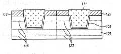
- a gap-fill dielectric filmis formed, fully filling the trench 107 , and then CMP (Chemical Mechanical Polishing) is performed until the nitride film 105 remains in a thickness of 1500 ⁇ 2500 ⁇ , thus forming the gap-fill dielectric film 111 in the trench.
- CMPChemical Mechanical Polishing
- the remaining nitride film 105is removed, for example by wet etching. As the nitride film 105 is removed, a pad oxide film 103 loses about 10% of its thickness.
- a photoresist pattern 113is formed to define a NMOS region, and plural ion-implantations, comprising a well ion implantation, a channel-stop ion implantation and a punch through ion implantation, are performed to form plural ion-implantation regions 115 in the NMOS region.
- the pad oxide filmis removed in the NMOS region, and photoresist pattern 113 is removed.
- an epitaxial layer 117 for controlling a threshold voltageis formed on the surface of an active region exposed in the NMOS region by SEG (Selective Epitaxial Growth) process.
- the epitaxial layer 117 for controlling a threshold voltagecan be formed, using a (halo)silane such as TCS (SiHCl 3 ) or dichlorosilane (SiH 2 Cl 2 ) under conditions comprising a temperature of 1000 ⁇ 1200° C., an atmospheric pressure of 760 torr (or such a pressure reduced by up to about 20 torr).
- the dopantis introduced in an amount effective to control the threshold voltage of a subsequently-formed transistor (e.g., to result in the epitaxial layer having a concentration of the dopant in a range conventional for threshold voltage implants; for example, providing a dopant dose of from 10 12 to 5 ⁇ 10 13 cm ⁇ 2 ).
- the epitaxial layer 117grows adjacent to gap-fill dielectric 111 , surrounding and/or interfacing with gap-fill dielectric 111 .
- the epitaxial layer 117may be formed before removing photoresist pattern 113 .
- an oxide film 119is formed having a thickness of 50 ⁇ 100 ⁇ over the substrate, by thermal growth or chemical vapor deposition (CVD).
- the oxide film 119functions to activate dopants in the epitaxial layer 117 .
- An additional oxide filmmay be formed on the pad oxide film 103 in a PMOS region, thus the pad oxide film 103 may be formed having a thickness of about 50 ⁇ 200 ⁇ .
- a photoresist pattern 121is formed to define a PMOS region, and plural ion implantation regions 123 are formed by performing ion implantations, comprising a well ion implantation, a channel-stop ion implantation and a punch through ion implantation. Thereafter, an active area of the PMOS region is exposed by removing the pad oxide film 103 in the PMOS region.
- an epitaxial layer 125 for controlling a threshold voltageis formed on the surface of an active region exposed in the PMOS region, using a SEG (Selective Epitaxial Growth) process as described with regard to FIG. 8 .
- the epitaxial layer 125 for controlling a threshold voltagecan be formed, using TCS (SiHCl 3 ) under conditions comprising a temperature of 1000 ⁇ 1200° C., an atmospheric pressure of 760 torr (or a pressure reduced by up to about 20 torr).
- the dopantis introduced in an amount effective to control the threshold voltage of a subsequently-formed transistor (e.g., to result in the epitaxial layer having a concentration of the dopant in a range conventional for threshold voltage implants; for example, providing a dopant dose of from 10 12 to 5 ⁇ 10 13 cm ⁇ 2 ).
- the epitaxial layer 125grows adjacent to gap-fill dielectric 111 , surrounding and/or interfacing with gap-fill dielectric 111 .
- the epitaxial layer 125may be formed before removing photoresist pattern 113 .
- the epitaxial layer 125can have a thickness of about 600 ⁇ 900 ⁇ on the active PMOS region because of the remaining oxide film 119 on the NMOS region. Therefore, corner portions of the liner oxide film 109 and the gap-fill dielectric film 111 may be protected by the epitaxial layers 117 and 125 in the subsequent cleaning process, and corner portions of the liner oxide film 109 and the gap-fill dielectric film 111 are generally not removed.
- the oxide film 119 on the NMOS regionis removed.
- the subsequent processesinvolve: forming a gate dielectric film on the epitaxial layers, either by (i) thermal growth or (ii) CVD and annealing; stacking (e.g., depositing) a gate conductive layer on the gate dielectric film; forming a gate electrode by patterning the gate conductive layer; and forming source/drain regions in the active area adjacent to the gate electrode, thus forming the MOS transistor.
Landscapes
- Engineering & Computer Science (AREA)
- Physics & Mathematics (AREA)
- Condensed Matter Physics & Semiconductors (AREA)
- General Physics & Mathematics (AREA)
- Manufacturing & Machinery (AREA)
- Computer Hardware Design (AREA)
- Microelectronics & Electronic Packaging (AREA)
- Power Engineering (AREA)
- Element Separation (AREA)
- Insulated Gate Type Field-Effect Transistor (AREA)
Abstract
Description
- This application claims the benefit of Korean Application No. 10-2005-0073735, filed on Aug. 11, 2005, which is incorporated by reference herein in its entirety.
- 1. Field of the Invention
- The present invention relates to a semiconductor device and a formation method thereof, and more particularly, to a semiconductor device and a method of fabricating the same, in which has an epitaxial layer for controlling a threshold voltage.
- 2. Description of the Related Art
- In general, various ion implantations are processed for embodying electric property of a MOS-transistor. Ion implantation is a process wherein impurity atoms are ionized and accelerated in an electric field to be implanted into a wafer, for the sake of substituting an impurity doping process by a high-temperature diffusion in a semiconductor device.
- Ion implantation is both to control a dose of the impurity accurately and to control a distribution shape of the implanted ions. Additionally, Ion implantation has advantages that a lateral spread phenomenon is reduced in contrast to the high-temperature diffusion and a uniformity of impurity concentration in the wafer is excellent.
- Ion implantation is used for threshold voltage control, punch through prevention, well formation, or isolation of circuit elements, etc., in MOS (Metal Oxide Semiconductor) transistors, and also for resistor formation, base formation, and isolation of devices, etc., in bipolar transistors.
- However, the ions injected in the ion implantation apparatus are collided with a wafer, which can induce strains and defects. In order to overcome such problems, an annealing process is generally performed.
- On the other hand, the semiconductor device generally comprises various electronic elements, such as transistors and capacitors formed on the semiconductor substrate, and wires that connect them with each other. To integrate such elements on the semiconductor substrate, it preferentially needs to isolate electrically regions where various electronic elements are formed, which is so-called “a device isolation.”
- LOCOS (Local Oxidation of Silicon) method, widely known as an isolation technique, involves forming an isolating oxide film on a field area to electrically isolate device active areas. However, a bird's beak phenomenon in the field area may occur. Namely, peripheral portions of the isolating oxide film may spread to reduce the active areas where circuit elements will be formed, thus resulting in decreasing a channel length and a punch through.
- Recently, a STI (Shallow Trench Isolation) technique has been widely used to solve these problems. Advantages of the STI technique are both to minimize formation areas of dielectric films and to form a stable isolation structure. To explain isolation method using the STI technique, a silicon nitride film is firstly deposited on a semiconductor substrate on which an oxide thin film is previously formed, and it is patterned. Next, using the silicon nitride film as an etch-mask, the semiconductor substrate is etched to form a trench. After that, a liner oxide film is formed inside of the trench, and then the trench is sufficiently filled with a silicon oxide material. CMP (Chemical Mechanical Polishing) process is performed to planarize the patterned silicon nitride film until a surface thereof is exposed. Therefore, active areas in the semiconductor substrate are isolated by the silicon oxide film. For following processes in the isolated state, the patterned silicon nitride film remaining in the active area is removed.
- However, there are such problems as the liner oxide film may be etched during a cleaning process prior to fabrication of a gate dielectric film. Moreover, a moat phenomenon, in which a STI gap-fill oxide film is etched, can also occur.
- It is, therefore, an object of the present invention to provide a semiconductor device and a fabrication method thereof, in which a surface damage of a semiconductor substrate can be prevented that might otherwise occur during an ion implantation for controlling a threshold voltage. Especially, the present invention does not need to perform an annealing step after ion implantation.
- In addition, another object of the present invention is to provide a semiconductor device and a fabrication method thereof, in which an isolation effect is enhanced by protecting an oxide film at a corner of a STI, thus preventing an occurrence or reducing the incidence and/or effect(s) of a moat phenomenon in the STI and damage to a gap-fill dielectric film.
- To achieve the above objects, an embodiment of a formation method of fabricating the semiconductor device comprises the steps of: forming a pad oxide film and a nitride film on a semiconductor substrate; exposing the semiconductor substrate by selectively etching the pad oxide film and the nitride film; forming a trench in the exposed semiconductor substrate; forming a gap-fill dielectric film in the trench; exposing an active area of the semiconductor substrate by removing the pad oxide film and the nitride film; forming an epitaxial layer (for controlling a threshold voltage) including a dopant in the exposed active area; forming a gate conductive layer on a gate dielectric film on the epitaxial layer; forming a gate electrode by patterning the gate conductive layer; and forming a source region and a drain region at the active area beside the gate electrode.
- According to the present invention, it is preferable to form the epitaxial layer horizontally surrounding the gap-fill dielectric film. Also, the liner oxide film can be formed in the trench after forming the trench. Additionally, the ion implantation can be performed before exposing the active area of the semiconductor substrate.
- As described above, the present invention can reduce or prevent surface damage to a semiconductor substrate, which may occur when of performing an ion implantation for controlling a threshold voltage. Furthermore, one does not need to perform an anneal after ion implantation.
- Moreover, the present invention can enhance an isolation effect by protecting an oxide film in a corner of the STI, to reduce or prevent the occurrence and/or effect(s) of a moat phenomenon in the STI, and to reduce or prevent damage to the gap-fill dielectric film.
- FIGS.1 to12 are cross-sectional views illustrating a method for fabricating a semiconductor device according to an embodiment of the present invention.
- Hereinafter, a preferred embodiment of the present invention will be described in detail with reference to the accompanying drawings. A shape and thickness of a layer and a member are exaggerated or schematic in the drawings. The same reference numerals are used throughout the drawings to indicate the same elements.
- Referring to
FIG. 1 , apad oxide film 103 is formed in a thickness of 50˜150 Å on asemiconductor substrate 101, using an oxygen gas and a hydrogen gas. Thepad oxide film 103 mitigates stresses of thesemiconductor substrate 101 and a nitride film to be formed hereafter, and protects thesemiconductor substrate 101 in an ion implantation process, and further participates in a project region Rp of the ion implantation. - Referring to
FIG. 2 , anitride film 105 is formed in a thickness of 1,000˜3,000 Å on thepad oxide film 103, using NH3gas and SiH2Cl2gas at a pressure of 0.2˜0.25 torr. Thenitride film 105 is used as an etch or polish stop layer for a subsequently-deposited gap-fill oxide film in the following process, i.e. a STI process. - As shown in
FIG. 3 , the semiconductor substrate is exposed by general photolithography and etching processes. Specifically, the pad oxide film and the nitride film are selectively etched to expose a portion of the semiconductor substrate. Continuously, atrench 107 is formed having a depth of about 4,500 Ř6,000 Šby etching the exposed semiconductor substrate. - Subsequently, a
liner oxide film 109 is formed by thermally oxidizing a surface of thetrench 107 using an oxygen gas or a mixed gas of oxygen and hydrogen at a temperature of from 700° C. to 950° C. Theliner oxide film 109 may have a predetermined thickness, for example, 100˜250 Å. Theliner oxide film 109 reduces etching damage that may have resulted from the trench formation process, and helps to form the gap-fill oxide film more easily. - As shown in
FIG. 4 , a gap-fill dielectric film is formed, fully filling thetrench 107, and then CMP (Chemical Mechanical Polishing) is performed until thenitride film 105 remains in a thickness of 1500˜2500 Å, thus forming the gap-filldielectric film 111 in the trench. - As shown in
FIG. 5 , theremaining nitride film 105 is removed, for example by wet etching. As thenitride film 105 is removed, apad oxide film 103 loses about 10% of its thickness. - As shown in
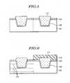
FIG. 6 , aphotoresist pattern 113 is formed to define a NMOS region, and plural ion-implantations, comprising a well ion implantation, a channel-stop ion implantation and a punch through ion implantation, are performed to form plural ion-implantation regions 115 in the NMOS region. - As shown in
FIG. 7 , the pad oxide film is removed in the NMOS region, andphotoresist pattern 113 is removed. - Referring to
FIG. 8 , anepitaxial layer 117 for controlling a threshold voltage is formed on the surface of an active region exposed in the NMOS region by SEG (Selective Epitaxial Growth) process. Theepitaxial layer 117 for controlling a threshold voltage can be formed, using a (halo)silane such as TCS (SiHCl3) or dichlorosilane (SiH2Cl2) under conditions comprising a temperature of 1000˜1200° C., an atmospheric pressure of 760 torr (or such a pressure reduced by up to about 20 torr). Additionally, theepitaxial layer 117 can be doped using a (sila)borane such as B2H6, B5H9, B6H10or (H3Si)xBHy(1≦x≦3, and x+y=3) as a dopant by introducing the (sila)borane gas into the epitaxy atmosphere and/or chamber. Generally, the dopant is introduced in an amount effective to control the threshold voltage of a subsequently-formed transistor (e.g., to result in the epitaxial layer having a concentration of the dopant in a range conventional for threshold voltage implants; for example, providing a dopant dose of from 1012to 5×1013cm−2). Since epitaxial silicon does not grow on silicon dioxide (e.g., gap-fill dielectric111), and thesubstrate 101 adjacent to gap-fill dielectric111 is exposed, theepitaxial layer 117 grows adjacent to gap-fill dielectric111, surrounding and/or interfacing with gap-fill dielectric111. In addition, theepitaxial layer 117 may be formed before removingphotoresist pattern 113. - Referring to
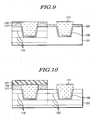
FIG. 9 , anoxide film 119 is formed having a thickness of 50˜100 Å over the substrate, by thermal growth or chemical vapor deposition (CVD). Theoxide film 119 functions to activate dopants in theepitaxial layer 117. An additional oxide film may be formed on thepad oxide film 103 in a PMOS region, thus thepad oxide film 103 may be formed having a thickness of about 50˜200 Å. - Referring to
FIG. 10 , aphotoresist pattern 121 is formed to define a PMOS region, and pluralion implantation regions 123 are formed by performing ion implantations, comprising a well ion implantation, a channel-stop ion implantation and a punch through ion implantation. Thereafter, an active area of the PMOS region is exposed by removing thepad oxide film 103 in the PMOS region. - Referring to
FIG. 11 , anepitaxial layer 125 for controlling a threshold voltage is formed on the surface of an active region exposed in the PMOS region, using a SEG (Selective Epitaxial Growth) process as described with regard toFIG. 8 . Theepitaxial layer 125 for controlling a threshold voltage can be formed, using TCS (SiHCl3) under conditions comprising a temperature of 1000˜1200° C., an atmospheric pressure of 760 torr (or a pressure reduced by up to about 20 torr). Additionally, theepitaxial layer 125 can be doped using a (sila)phosphine such as PH3or (H3Si)xPHy(1≦x≦3, and x+y=3) as a dopant by introducing the (sila)phosphine gas into the epitaxy atmosphere and/or chamber. Generally, the dopant is introduced in an amount effective to control the threshold voltage of a subsequently-formed transistor (e.g., to result in the epitaxial layer having a concentration of the dopant in a range conventional for threshold voltage implants; for example, providing a dopant dose of from 1012to 5×1013cm−2). As described with regard toFIG. 8 , theepitaxial layer 125 grows adjacent to gap-fill dielectric 111, surrounding and/or interfacing with gap-fill dielectric 111. In addition, theepitaxial layer 125 may be formed before removingphotoresist pattern 113. - The
epitaxial layer 125 can have a thickness of about 600˜900 Å on the active PMOS region because of the remainingoxide film 119 on the NMOS region. Therefore, corner portions of theliner oxide film 109 and the gap-fill dielectric film 111 may be protected by theepitaxial layers liner oxide film 109 and the gap-fill dielectric film 111 are generally not removed. - Referring to
FIG. 12 , theoxide film 119 on the NMOS region is removed. - Hereinafter, subsequent processes are performed according to typical manufacturing processes of a general MOS transistor. Namely, the subsequent processes involve: forming a gate dielectric film on the epitaxial layers, either by (i) thermal growth or (ii) CVD and annealing; stacking (e.g., depositing) a gate conductive layer on the gate dielectric film; forming a gate electrode by patterning the gate conductive layer; and forming source/drain regions in the active area adjacent to the gate electrode, thus forming the MOS transistor.
- While the invention has been particularly shown and described with reference to the preferred embodiments thereof, it will be understood by those skilled in the art that various changes in form and detail may be made therein without departing from the sprit and scope of the invention as defined by the appended claims.
Claims (17)
Applications Claiming Priority (2)
| Application Number | Priority Date | Filing Date | Title |
|---|---|---|---|
| KR10-2005-0073735 | 2005-08-11 | ||
| KR1020050073735AKR100683401B1 (en) | 2005-08-11 | 2005-08-11 | Semiconductor Device Using Epilayer and Manufacturing Method Thereof |
Publications (2)
| Publication Number | Publication Date |
|---|---|
| US20070037360A1true US20070037360A1 (en) | 2007-02-15 |
| US7514337B2 US7514337B2 (en) | 2009-04-07 |
Family
ID=37743057
Family Applications (1)
| Application Number | Title | Priority Date | Filing Date |
|---|---|---|---|
| US11/503,020Active2026-10-03US7514337B2 (en) | 2005-08-11 | 2006-08-11 | Semiconductor device using EPI-layer and method of forming the same |
Country Status (2)
| Country | Link |
|---|---|
| US (1) | US7514337B2 (en) |
| KR (1) | KR100683401B1 (en) |
Cited By (8)
| Publication number | Priority date | Publication date | Assignee | Title |
|---|---|---|---|---|
| US20090162990A1 (en)* | 2007-12-21 | 2009-06-25 | Sang Tae Ahn | Method for manufacturing a semiconductor device capable of preventing the decrease of the width of an active region |
| US20110260047A1 (en)* | 2010-04-21 | 2011-10-27 | Axcelis Technologies, Inc. | Silaborane implantation processes |
| WO2017161236A1 (en)* | 2016-03-17 | 2017-09-21 | Applied Materials, Inc. | Methods for gapfill in high aspect ratio structures |
| WO2018164746A3 (en)* | 2016-11-29 | 2018-12-06 | SemiNuclear, Inc. | Process and manufacture of low-dimensional materials supporting both self-thermalization and self-localization |
| US11133178B2 (en) | 2019-09-20 | 2021-09-28 | Applied Materials, Inc. | Seamless gapfill with dielectric ALD films |
| US11521853B2 (en) | 2015-05-28 | 2022-12-06 | SemiNuclear, Inc. | Composition and method for making picocrystalline artificial borane atoms |
| US11651957B2 (en) | 2015-05-28 | 2023-05-16 | SemiNuclear, Inc. | Process and manufacture of low-dimensional materials supporting both self-thermalization and self-localization |
| CN118884783A (en)* | 2024-08-26 | 2024-11-01 | 浙江创芯集成电路有限公司 | A method for checking whether photoresist can block ion implantation |
Families Citing this family (4)
| Publication number | Priority date | Publication date | Assignee | Title |
|---|---|---|---|---|
| JP2011044503A (en)* | 2009-08-19 | 2011-03-03 | Sharp Corp | Method of manufacturing semiconductor device, and semiconductor device |
| US20110084355A1 (en)* | 2009-10-09 | 2011-04-14 | Taiwan Semiconductor Manufacturing Company, Ltd. | Isolation Structure For Semiconductor Device |
| CN102122631A (en)* | 2010-01-08 | 2011-07-13 | 上海华虹Nec电子有限公司 | Method for obtaining air gap trench |
| US11848339B2 (en)* | 2021-03-19 | 2023-12-19 | Taiwan Semiconductor Manufacturing Company Ltd. | Semiconductor structure including isolation structure and method for forming isolation structure |
Citations (6)
| Publication number | Priority date | Publication date | Assignee | Title |
|---|---|---|---|---|
| US5763314A (en)* | 1994-11-30 | 1998-06-09 | Lucent Technologies Inc. | Process for forming isolation regions in an integrated circuit |
| US6005279A (en)* | 1997-12-18 | 1999-12-21 | Advanced Micro Devices, Inc. | Trench edge spacer formation |
| US6051469A (en)* | 1998-04-18 | 2000-04-18 | United Semiconductor Corp. | Method of fabricating bit line |
| US6432781B2 (en)* | 2000-06-19 | 2002-08-13 | Texas Instruments Incorporated | Inverted MOSFET process |
| US20060131689A1 (en)* | 2004-12-17 | 2006-06-22 | Fujitsu Limited | Semiconductor device and fabrication method thereof |
| US7170109B2 (en)* | 2003-06-13 | 2007-01-30 | Renesas Technology Corp. | Heterojunction semiconductor device with element isolation structure |
Family Cites Families (2)
| Publication number | Priority date | Publication date | Assignee | Title |
|---|---|---|---|---|
| KR100756774B1 (en)* | 2001-06-22 | 2007-09-07 | 주식회사 하이닉스반도체 | Manufacturing method of semiconductor device |
| KR100431302B1 (en)* | 2002-05-07 | 2004-05-12 | 주식회사 하이닉스반도체 | Method of manufacturing system on chip device |
- 2005
- 2005-08-11KRKR1020050073735Apatent/KR100683401B1/ennot_activeExpired - Fee Related
- 2006
- 2006-08-11USUS11/503,020patent/US7514337B2/enactiveActive
Patent Citations (6)
| Publication number | Priority date | Publication date | Assignee | Title |
|---|---|---|---|---|
| US5763314A (en)* | 1994-11-30 | 1998-06-09 | Lucent Technologies Inc. | Process for forming isolation regions in an integrated circuit |
| US6005279A (en)* | 1997-12-18 | 1999-12-21 | Advanced Micro Devices, Inc. | Trench edge spacer formation |
| US6051469A (en)* | 1998-04-18 | 2000-04-18 | United Semiconductor Corp. | Method of fabricating bit line |
| US6432781B2 (en)* | 2000-06-19 | 2002-08-13 | Texas Instruments Incorporated | Inverted MOSFET process |
| US7170109B2 (en)* | 2003-06-13 | 2007-01-30 | Renesas Technology Corp. | Heterojunction semiconductor device with element isolation structure |
| US20060131689A1 (en)* | 2004-12-17 | 2006-06-22 | Fujitsu Limited | Semiconductor device and fabrication method thereof |
Cited By (17)
| Publication number | Priority date | Publication date | Assignee | Title |
|---|---|---|---|---|
| US20090162990A1 (en)* | 2007-12-21 | 2009-06-25 | Sang Tae Ahn | Method for manufacturing a semiconductor device capable of preventing the decrease of the width of an active region |
| US8530330B2 (en)* | 2007-12-21 | 2013-09-10 | Hynix Semiconductor Inc. | Method for manufacturing a semiconductor device capable of preventing the decrease of the width of an active region |
| US20110260047A1 (en)* | 2010-04-21 | 2011-10-27 | Axcelis Technologies, Inc. | Silaborane implantation processes |
| CN102844842A (en)* | 2010-04-21 | 2012-12-26 | 艾克塞利斯科技公司 | Silicon borane implantation method |
| US8344337B2 (en)* | 2010-04-21 | 2013-01-01 | Axcelis Technologies, Inc. | Silaborane implantation processes |
| CN102844842B (en)* | 2010-04-21 | 2016-01-27 | 艾克塞利斯科技公司 | Silaborane Injection Method |
| US11651957B2 (en) | 2015-05-28 | 2023-05-16 | SemiNuclear, Inc. | Process and manufacture of low-dimensional materials supporting both self-thermalization and self-localization |
| US11521853B2 (en) | 2015-05-28 | 2022-12-06 | SemiNuclear, Inc. | Composition and method for making picocrystalline artificial borane atoms |
| KR102312824B1 (en) | 2016-03-17 | 2021-10-13 | 어플라이드 머티어리얼스, 인코포레이티드 | Methods for Gap Filling in High Aspect Ratio Structures |
| US10192775B2 (en) | 2016-03-17 | 2019-01-29 | Applied Materials, Inc. | Methods for gapfill in high aspect ratio structures |
| US10811303B2 (en) | 2016-03-17 | 2020-10-20 | Applied Materials, Inc. | Methods for gapfill in high aspect ratio structures |
| US11488856B2 (en) | 2016-03-17 | 2022-11-01 | Applied Materials, Inc. | Methods for gapfill in high aspect ratio structures |
| KR20180117714A (en)* | 2016-03-17 | 2018-10-29 | 어플라이드 머티어리얼스, 인코포레이티드 | Methods for gap filling in high aspect ratio structures |
| WO2017161236A1 (en)* | 2016-03-17 | 2017-09-21 | Applied Materials, Inc. | Methods for gapfill in high aspect ratio structures |
| WO2018164746A3 (en)* | 2016-11-29 | 2018-12-06 | SemiNuclear, Inc. | Process and manufacture of low-dimensional materials supporting both self-thermalization and self-localization |
| US11133178B2 (en) | 2019-09-20 | 2021-09-28 | Applied Materials, Inc. | Seamless gapfill with dielectric ALD films |
| CN118884783A (en)* | 2024-08-26 | 2024-11-01 | 浙江创芯集成电路有限公司 | A method for checking whether photoresist can block ion implantation |
Also Published As
| Publication number | Publication date |
|---|---|
| KR100683401B1 (en) | 2007-02-15 |
| US7514337B2 (en) | 2009-04-07 |
Similar Documents
| Publication | Publication Date | Title |
|---|---|---|
| US7514337B2 (en) | Semiconductor device using EPI-layer and method of forming the same | |
| US8030173B2 (en) | Silicon nitride hardstop encapsulation layer for STI region | |
| US6440807B1 (en) | Surface engineering to prevent EPI growth on gate poly during selective EPI processing | |
| US10032663B1 (en) | Anneal after trench sidewall implant to reduce defects | |
| US6773970B2 (en) | Method of producing a semiconductor device having improved gate structure | |
| US20080268602A1 (en) | Method of fabricating semiconductor device | |
| US7129127B2 (en) | Integration scheme to improve NMOS with poly cap while mitigating PMOS degradation | |
| US6075258A (en) | Elevated transistor fabrication technique | |
| US6326272B1 (en) | Method for forming self-aligned elevated transistor | |
| US10347626B2 (en) | High quality deep trench oxide | |
| US7190007B2 (en) | Isolated fully depleted silicon-on-insulator regions by selective etch | |
| US5208181A (en) | Locos isolation scheme for small geometry or high voltage circuit | |
| US6753232B2 (en) | Method for fabricating semiconductor device | |
| US6391733B1 (en) | Method of doping semiconductor devices through a layer of dielectric material | |
| WO2007035660A1 (en) | Method to form a device on a soi substrate | |
| US5913115A (en) | Method for producing a CMOS circuit | |
| US6162714A (en) | Method of forming thin polygates for sub quarter micron CMOS process | |
| US20100032813A1 (en) | Ic formed with densified chemical oxide layer | |
| US9412869B2 (en) | MOSFET with source side only stress | |
| US6284608B1 (en) | Method for making accumulation mode N-channel SOI | |
| US6800514B2 (en) | Method of fabricating a MOS transistor with a drain extension and corresponding transistor | |
| KR100613286B1 (en) | Method of manufacturing semiconductor device using epitaxial process | |
| KR19990074005A (en) | Trench Device Isolation Method to Prevent Impurity Diffusion from Well Area | |
| KR100382556B1 (en) | Method for manufacturing isolation of semiconductor device | |
| KR100691129B1 (en) | Manufacturing Method of Semiconductor Device |
Legal Events
| Date | Code | Title | Description |
|---|---|---|---|
| AS | Assignment | Owner name:DONGBU ELECTRONICS CO, LTD., KOREA, REPUBLIC OF Free format text:ASSIGNMENT OF ASSIGNORS INTEREST;ASSIGNOR:JEONG, DAE HO;REEL/FRAME:018202/0184 Effective date:20060811 | |
| FEPP | Fee payment procedure | Free format text:PAYOR NUMBER ASSIGNED (ORIGINAL EVENT CODE: ASPN); ENTITY STATUS OF PATENT OWNER: LARGE ENTITY | |
| STCF | Information on status: patent grant | Free format text:PATENTED CASE | |
| FPAY | Fee payment | Year of fee payment:4 | |
| FPAY | Fee payment | Year of fee payment:8 | |
| AS | Assignment | Owner name:DONGBU HITEK CO., LTD., KOREA, REPUBLIC OF Free format text:MERGER AND CHANGE OF NAME;ASSIGNORS:DONGBU ELECTRONICS CO., LTD.;DONGBU HITEK CO., LTD.;REEL/FRAME:044533/0523 Effective date:20070503 | |
| AS | Assignment | Owner name:DB HITEK CO., LTD, KOREA, REPUBLIC OF Free format text:CHANGE OF NAME;ASSIGNOR:DONGBU HITEK CO., LTD.;REEL/FRAME:044555/0913 Effective date:20171101 | |
| AS | Assignment | Owner name:COLUMBA TECHNOLOGIES INC., CANADA Free format text:ASSIGNMENT OF ASSIGNORS INTEREST;ASSIGNOR:DB HITEK CO., LTD.;REEL/FRAME:049709/0857 Effective date:20190125 | |
| AS | Assignment | Owner name:TAIWAN SEMICONDUCTOR MANUFACTURING CO., LTD., TAIWAN Free format text:ASSIGNMENT OF ASSIGNORS INTEREST;ASSIGNOR:COLUMBA TECHNOLOGIES, INC.;REEL/FRAME:052845/0474 Effective date:20200211 | |
| MAFP | Maintenance fee payment | Free format text:PAYMENT OF MAINTENANCE FEE, 12TH YEAR, LARGE ENTITY (ORIGINAL EVENT CODE: M1553); ENTITY STATUS OF PATENT OWNER: LARGE ENTITY Year of fee payment:12 |