US20070034898A1 - Heterojunction photodiode - Google Patents
Heterojunction photodiodeDownload PDFInfo
- Publication number
- US20070034898A1 US20070034898A1US11/031,803US3180305AUS2007034898A1US 20070034898 A1US20070034898 A1US 20070034898A1US 3180305 AUS3180305 AUS 3180305AUS 2007034898 A1US2007034898 A1US 2007034898A1
- Authority
- US
- United States
- Prior art keywords
- photodiode
- region
- material region
- junction
- bias voltage
- Prior art date
- Legal status (The legal status is an assumption and is not a legal conclusion. Google has not performed a legal analysis and makes no representation as to the accuracy of the status listed.)
- Granted
Links
- 239000000463materialSubstances0.000claimsabstractdescription63
- 238000003384imaging methodMethods0.000claimsabstractdescription6
- 230000004888barrier functionEffects0.000claimsdescription19
- 229910000661Mercury cadmium tellurideInorganic materials0.000claimsdescription9
- 238000002161passivationMethods0.000claimsdescription8
- 238000009792diffusion processMethods0.000claimsdescription7
- 230000007423decreaseEffects0.000claimsdescription5
- 239000002019doping agentSubstances0.000claimsdescription5
- 230000004044responseEffects0.000claimsdescription5
- MCMSPRNYOJJPIZ-UHFFFAOYSA-Ncadmium;mercury;telluriumChemical compound[Cd]=[Te]=[Hg]MCMSPRNYOJJPIZ-UHFFFAOYSA-N0.000claimsdescription3
- 238000013459approachMethods0.000claimsdescription2
- 238000002347injectionMethods0.000claims3
- 239000007924injectionSubstances0.000claims3
- 230000004913activationEffects0.000claims2
- 229910000645Hg alloyInorganic materials0.000claims1
- 230000007547defectEffects0.000abstractdescription21
- 238000000034methodMethods0.000abstractdescription9
- 230000008569processEffects0.000abstractdescription7
- 238000005215recombinationMethods0.000description9
- 239000000758substrateSubstances0.000description9
- 230000006798recombinationEffects0.000description8
- 239000000969carrierSubstances0.000description7
- 229910052751metalInorganic materials0.000description6
- 239000002184metalSubstances0.000description6
- 239000006096absorbing agentSubstances0.000description5
- 239000004065semiconductorSubstances0.000description5
- 230000008901benefitEffects0.000description4
- 230000006870functionEffects0.000description4
- 230000003287optical effectEffects0.000description4
- MARUHZGHZWCEQU-UHFFFAOYSA-N5-phenyl-2h-tetrazoleChemical compoundC1=CC=CC=C1C1=NNN=N1MARUHZGHZWCEQU-UHFFFAOYSA-N0.000description3
- 238000010586diagramMethods0.000description3
- 238000005468ion implantationMethods0.000description3
- 150000002739metalsChemical class0.000description3
- 229910004262HgTeInorganic materials0.000description2
- -1MnSeInorganic materials0.000description2
- 229910000577Silicon-germaniumInorganic materials0.000description2
- 238000010521absorption reactionMethods0.000description2
- 229910045601alloyInorganic materials0.000description2
- 239000000956alloySubstances0.000description2
- FTWRSWRBSVXQPI-UHFFFAOYSA-Nalumanylidynearsane;gallanylidynearsaneChemical compound[As]#[Al].[As]#[Ga]FTWRSWRBSVXQPI-UHFFFAOYSA-N0.000description2
- 230000015572biosynthetic processEffects0.000description2
- 239000002800charge carrierSubstances0.000description2
- 238000000151depositionMethods0.000description2
- 238000001514detection methodMethods0.000description2
- 230000000694effectsEffects0.000description2
- 238000002513implantationMethods0.000description2
- 239000012535impuritySubstances0.000description2
- 239000011572manganeseSubstances0.000description2
- 230000007246mechanismEffects0.000description2
- 239000011669seleniumSubstances0.000description2
- JBRZTFJDHDCESZ-UHFFFAOYSA-NAsGaChemical compound[As]#[Ga]JBRZTFJDHDCESZ-UHFFFAOYSA-N0.000description1
- PWHULOQIROXLJO-UHFFFAOYSA-NManganeseChemical compound[Mn]PWHULOQIROXLJO-UHFFFAOYSA-N0.000description1
- 229910017231MnTeInorganic materials0.000description1
- BUGBHKTXTAQXES-UHFFFAOYSA-NSeleniumChemical compound[Se]BUGBHKTXTAQXES-UHFFFAOYSA-N0.000description1
- XUIMIQQOPSSXEZ-UHFFFAOYSA-NSiliconChemical compound[Si]XUIMIQQOPSSXEZ-UHFFFAOYSA-N0.000description1
- 229910007709ZnTeInorganic materials0.000description1
- LEVVHYCKPQWKOP-UHFFFAOYSA-N[Si].[Ge]Chemical compound[Si].[Ge]LEVVHYCKPQWKOP-UHFFFAOYSA-N0.000description1
- 238000000137annealingMethods0.000description1
- 229910052793cadmiumInorganic materials0.000description1
- BDOSMKKIYDKNTQ-UHFFFAOYSA-Ncadmium atomChemical compound[Cd]BDOSMKKIYDKNTQ-UHFFFAOYSA-N0.000description1
- UHYPYGJEEGLRJD-UHFFFAOYSA-Ncadmium(2+);selenium(2-)Chemical compound[Se-2].[Cd+2]UHYPYGJEEGLRJD-UHFFFAOYSA-N0.000description1
- 238000004891communicationMethods0.000description1
- 230000006854communicationEffects0.000description1
- 150000001875compoundsChemical class0.000description1
- 238000001816coolingMethods0.000description1
- 230000007812deficiencyEffects0.000description1
- 230000008021depositionEffects0.000description1
- 230000005684electric fieldEffects0.000description1
- 238000005516engineering processMethods0.000description1
- 230000007613environmental effectEffects0.000description1
- 238000005530etchingMethods0.000description1
- 229910052737goldInorganic materials0.000description1
- 238000005286illuminationMethods0.000description1
- 150000002500ionsChemical class0.000description1
- 230000031700light absorptionEffects0.000description1
- 229910052748manganeseInorganic materials0.000description1
- 238000004519manufacturing processMethods0.000description1
- 238000005259measurementMethods0.000description1
- QSHDDOUJBYECFT-UHFFFAOYSA-NmercuryChemical compound[Hg]QSHDDOUJBYECFT-UHFFFAOYSA-N0.000description1
- 229910052753mercuryInorganic materials0.000description1
- 238000001465metallisationMethods0.000description1
- 239000000203mixtureSubstances0.000description1
- 238000012986modificationMethods0.000description1
- 230000004048modificationEffects0.000description1
- 238000012544monitoring processMethods0.000description1
- 230000004297night visionEffects0.000description1
- 230000005693optoelectronicsEffects0.000description1
- 229910052763palladiumInorganic materials0.000description1
- 229910052697platinumInorganic materials0.000description1
- 238000004886process controlMethods0.000description1
- 238000012545processingMethods0.000description1
- 230000005855radiationEffects0.000description1
- 230000008707rearrangementEffects0.000description1
- 230000009467reductionEffects0.000description1
- 150000003839saltsChemical class0.000description1
- 229910052711seleniumInorganic materials0.000description1
- SBIBMFFZSBJNJF-UHFFFAOYSA-Nselenium;zincChemical compound[Se]=[Zn]SBIBMFFZSBJNJF-UHFFFAOYSA-N0.000description1
- 230000035945sensitivityEffects0.000description1
- 229910052710siliconInorganic materials0.000description1
- 239000010703siliconSubstances0.000description1
- 238000010408sweepingMethods0.000description1
- JBQYATWDVHIOAR-UHFFFAOYSA-NtellanylidenegermaniumChemical compound[Te]=[Ge]JBQYATWDVHIOAR-UHFFFAOYSA-N0.000description1
- 239000010409thin filmSubstances0.000description1
- 230000007704transitionEffects0.000description1
- 230000005641tunnelingEffects0.000description1
Images


Classifications
- H—ELECTRICITY
- H10—SEMICONDUCTOR DEVICES; ELECTRIC SOLID-STATE DEVICES NOT OTHERWISE PROVIDED FOR
- H10F—INORGANIC SEMICONDUCTOR DEVICES SENSITIVE TO INFRARED RADIATION, LIGHT, ELECTROMAGNETIC RADIATION OF SHORTER WAVELENGTH OR CORPUSCULAR RADIATION
- H10F30/00—Individual radiation-sensitive semiconductor devices in which radiation controls the flow of current through the devices, e.g. photodetectors
- H10F30/20—Individual radiation-sensitive semiconductor devices in which radiation controls the flow of current through the devices, e.g. photodetectors the devices having potential barriers, e.g. phototransistors
- H10F30/21—Individual radiation-sensitive semiconductor devices in which radiation controls the flow of current through the devices, e.g. photodetectors the devices having potential barriers, e.g. phototransistors the devices being sensitive to infrared, visible or ultraviolet radiation
- H10F30/24—Individual radiation-sensitive semiconductor devices in which radiation controls the flow of current through the devices, e.g. photodetectors the devices having potential barriers, e.g. phototransistors the devices being sensitive to infrared, visible or ultraviolet radiation the devices having only two potential barriers, e.g. bipolar phototransistors
- H—ELECTRICITY
- H10—SEMICONDUCTOR DEVICES; ELECTRIC SOLID-STATE DEVICES NOT OTHERWISE PROVIDED FOR
- H10F—INORGANIC SEMICONDUCTOR DEVICES SENSITIVE TO INFRARED RADIATION, LIGHT, ELECTROMAGNETIC RADIATION OF SHORTER WAVELENGTH OR CORPUSCULAR RADIATION
- H10F30/00—Individual radiation-sensitive semiconductor devices in which radiation controls the flow of current through the devices, e.g. photodetectors
- H10F30/20—Individual radiation-sensitive semiconductor devices in which radiation controls the flow of current through the devices, e.g. photodetectors the devices having potential barriers, e.g. phototransistors
- H10F30/21—Individual radiation-sensitive semiconductor devices in which radiation controls the flow of current through the devices, e.g. photodetectors the devices having potential barriers, e.g. phototransistors the devices being sensitive to infrared, visible or ultraviolet radiation
- H10F30/22—Individual radiation-sensitive semiconductor devices in which radiation controls the flow of current through the devices, e.g. photodetectors the devices having potential barriers, e.g. phototransistors the devices being sensitive to infrared, visible or ultraviolet radiation the devices having only one potential barrier, e.g. photodiodes
- H10F30/221—Individual radiation-sensitive semiconductor devices in which radiation controls the flow of current through the devices, e.g. photodetectors the devices having potential barriers, e.g. phototransistors the devices being sensitive to infrared, visible or ultraviolet radiation the devices having only one potential barrier, e.g. photodiodes the potential barrier being a PN homojunction
- H10F30/2212—Individual radiation-sensitive semiconductor devices in which radiation controls the flow of current through the devices, e.g. photodetectors the devices having potential barriers, e.g. phototransistors the devices being sensitive to infrared, visible or ultraviolet radiation the devices having only one potential barrier, e.g. photodiodes the potential barrier being a PN homojunction the devices comprising active layers made of only Group II-VI materials, e.g. HgCdTe infrared photodiodes
- H—ELECTRICITY
- H10—SEMICONDUCTOR DEVICES; ELECTRIC SOLID-STATE DEVICES NOT OTHERWISE PROVIDED FOR
- H10F—INORGANIC SEMICONDUCTOR DEVICES SENSITIVE TO INFRARED RADIATION, LIGHT, ELECTROMAGNETIC RADIATION OF SHORTER WAVELENGTH OR CORPUSCULAR RADIATION
- H10F30/00—Individual radiation-sensitive semiconductor devices in which radiation controls the flow of current through the devices, e.g. photodetectors
- H10F30/20—Individual radiation-sensitive semiconductor devices in which radiation controls the flow of current through the devices, e.g. photodetectors the devices having potential barriers, e.g. phototransistors
- H10F30/21—Individual radiation-sensitive semiconductor devices in which radiation controls the flow of current through the devices, e.g. photodetectors the devices having potential barriers, e.g. phototransistors the devices being sensitive to infrared, visible or ultraviolet radiation
- H10F30/22—Individual radiation-sensitive semiconductor devices in which radiation controls the flow of current through the devices, e.g. photodetectors the devices having potential barriers, e.g. phototransistors the devices being sensitive to infrared, visible or ultraviolet radiation the devices having only one potential barrier, e.g. photodiodes
- H10F30/227—Individual radiation-sensitive semiconductor devices in which radiation controls the flow of current through the devices, e.g. photodetectors the devices having potential barriers, e.g. phototransistors the devices being sensitive to infrared, visible or ultraviolet radiation the devices having only one potential barrier, e.g. photodiodes the potential barrier being a Schottky barrier
- H—ELECTRICITY
- H10—SEMICONDUCTOR DEVICES; ELECTRIC SOLID-STATE DEVICES NOT OTHERWISE PROVIDED FOR
- H10F—INORGANIC SEMICONDUCTOR DEVICES SENSITIVE TO INFRARED RADIATION, LIGHT, ELECTROMAGNETIC RADIATION OF SHORTER WAVELENGTH OR CORPUSCULAR RADIATION
- H10F77/00—Constructional details of devices covered by this subclass
- H10F77/10—Semiconductor bodies
- H10F77/12—Active materials
- H10F77/123—Active materials comprising only Group II-VI materials, e.g. CdS, ZnS or HgCdTe
- H10F77/1237—Active materials comprising only Group II-VI materials, e.g. CdS, ZnS or HgCdTe having at least three elements, e.g. HgCdTe
Definitions
- This inventionrelates generally to optoelectronic devices and, more particularly, to infrared photodiode photodetectors.
- Photodetectorsare used in numerous applications to detect light and provide a corresponding electrical signal.
- Infrared (IR) photodetectorsare one class of detectors which are included in a variety of applications, such as night vision, communications, and environmental monitoring.
- IR detectorscan be based on several different material systems, including silicon (Si), gallium arsenide (GaAs), silicon germanium (SiGe), aluminum gallium arsenide (AlGaAs), lead salts (PbS, PbSeTe, PbSnTe), various Hg-bearing compounds, pseudobinary alloys of HgTe and HgSe with CdTe, CdSe, MnTe, MnSe, ZnTe, and ZnSe.
- Mercury cadmium telluride(HgCdTe or MCT) is attractive because it has a direct energy gap, can be grown as high-quality epitaxial thin films on transparent substrates, can be doped to obtain both high and low carrier concentrations, and spans the entire IR wavelength range from ⁇ 0.8 ⁇ m to >20 ⁇ m. It can also be compositionally graded to vary the bandgap energy with position. More information regarding MCT photodetectors can be found, for example, in U.S. Pat. No. 6,034,407.
- Photodiodesprovide the highest performance of all photodetectors.
- a photodiodeconsists of a semiconductor pn junction. The semiconductor absorbs light having photon energy higher than the semiconductor's bandgap, creating electron-hole pairs. If the light is absorbed in the n(p)-region, the holes (electrons) are the minority carriers and diffuse to the depletion region, where they are swept by the depletion region electric field into the p(n)-region to create a photocurrent that becomes the detector signal. Absorption of light in the depletion region produces this sweeping without need for diffusion.
- the fundamental quality of a detectoris its signal-to-noise ratio (SNR); i.e., the ratio of the photocurrent to the noise current present in the detector under measurement conditions.
- SNRsignal-to-noise ratio
- the highest quality a detector can have in any operating conditionis to have a SNR limited by the noise current that comes from the photon background itself. This condition is called “background-limited performance” or BLIP.
- BLIPbackground-limited performance
- the highest BLIP qualityis attained when every absorbed photon generates a minority carrier that contributes to the photocurrent.
- the efficiency of minority carrier collectionis called the quantum efficiency, and perfect detectors will have a quantum efficiency of 1.
- the pn-junctionis in a portion of the semiconductor structure with a wide bandgap (i.e., if the structure is a type of “heterostructure” having spatially varying energy gaps), under some conditions an energy barrier exists that frustrates diffusion of minority carriers to the depletion region and significantly reduces the photocurrent.
- the defects mentioned abovemay also cause the detectors to have too much noise.
- Dark currentwhich is a current that flows through the photodetector in the absence of incident light, adds noise to that inherent in the photocurrent, lowering the SNR below the BLIP level.
- the dark currentis caused by the thermal generation or tunneling of charge carriers due to fundamental mechanisms, to point defects, or to extended defects. It is generally desired to have the photodetector provide its maximum (BLIP) sensitivity at as high at temperature as possible, up to room temperature to avoid the need for elaborate cooling schemes.
- BLIPmaximum
- the thermally generated dark current-induced noisetypically increases exponentially with increasing operating temperature. Consequently, there is a need for a photodetector with fewer defects near the active region so that, at a given temperature, the quantum efficiency is improved and the defect-generated noise is reduced.
- the present inventionprovides a heterojunction photodiode which includes a pn junction formed in, or a Schottky-barrier junction formed on, a first wide bandgap material region.
- a heterojunction photodiodewhich includes a pn junction formed in, or a Schottky-barrier junction formed on, a first wide bandgap material region.
- the depletion region of the junctionexpands towards a second narrow bandgap material region, lowering the built-in barrier due to the heterostructure and allowing photocurrent to be generated efficiently.
- the dark currentis reduced compared to non-heterojunction devices because most process-induced defects and the highest fields of the depletion region are located in the wide bandgap region which has inherently low dark current, while the incident light is absorbed in the narrow field region where defects are few and applied fields are low. This lower dark current also reduces the noise in the total current flowing through the junction.
- the heterojunction photodiodecan be included in an imaging system
- FIG. 1is a simplified top view of an imaging system in accordance with the present invention
- FIG. 2is a simplified sectional view of a pn diode with a depletion region in accordance with the present invention
- FIG. 3is a simplified sectional view of a heterojunction photodiode with the pn diode illustrated in FIG. 2 ;
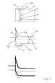
- FIG. 4is a graph showing the energy bands as a function of depth from the top surface of the device at various bias conditions for the heterojunction photodiode of FIG. 3 .
- FIG. 5is a graph which plots current versus voltage for a photodiode in accordance with the present invention.
- FIG. 6is a simplified sectional view of a Schottky-barrier heterojunction photodiode with a depletion region in accordance with the present invention.
- FIG. 7is a graph showing the energy bands as a function of depth from the top surface (along line 5 - 5 ′) of the device at zero and a nominal operational reverse bias condition for a Schottky-barrier version of the heterojunction photodiode of FIG. 6 .
- FIG. 1is a simplified top view of an imaging system 10 which includes an array 11 of pn or Schottky-barrier photodiodes 12 (interchangeably referred to herein as “photodetectors”).
- the photodetectors in array 11are formed on a substrate 13 , although they could be formed individually and mounted on a support structure.
- System 10can be included, for example, in a focal plane array (FPA), which is an optical sensor placed at the focal plane of an optical system such as a camera, spectrometer, or telescope.
- FPAfocal plane array
- the FPAis typically sensitive to ultraviolet, visible, or infrared radiation, although other wavelengths may also be detected.
- System 10would typically include circuitry 15 coupled to array 11 .
- Circuitry 15could include a read-out integrated circuit or a multiplexer which provides electronic access to the pixels in array 11 .
- array 11provides a signal SResponse to circuitry 15 for image processing.
- Circuitry 15can be external to system 10 , or it can be integrated with other components on substrate 13 , such as array 11 .
- junctions of photodiodes 12can be formed as pn junctions by numerous well-known methods, including ion implantation, diffusion doping, or by doping during growth. Alternatively, they can be formed as Schottky barrier junctions by depositing any of several metals or semi-metals on the heterostructure. Typically suitable metals would be ones with a large work function, such as Au, Pt, Pd, or other metals known to those in the field. Semimetals such as HgTe may also make appropriate Schottky barriers.
- passivationis used to protect the delicate junction from its environment, and metallization allows a contacting of the junction to external circuitry.
- the delineation process and layer bandgap profilesare chosen to allow surface passivation of the junction perimeter to be applied entirely in the region in which the junction is formed.
- these process stepsin addition to performing their intended functions, create a number of point and extended defects, which increase the amount of undesired recombination and dark currents in the detector structure.
- ion implantationincreases the number of point defects because it causes damage to the lattice which often results in vacancies, interstitial atoms, dislocation loops, and microscopic voids.
- Passivationcan induce surface deficiencies of cadmium and mercury, impurities, and amorphous or polycrystalline structures.
- the present photodiodeis formed so that the depletion region formed when the device is reverse-biased extends away from the regions of the device with the most defects, which are typically near its surface. Moreover, these higher defect regions are confined in wider bandgap material placed near the surface to suppress the effects of defects.
- the implanted ionsflow through the surface and into the near-surface wide bandgap material, such that the highest concentration of damage is near the surface in the widest bandgap material.
- the present photodiode's structure(discussed in detail below) comprises a pn or Schottky-barrier junction formed in a wide bandgap material region, with a second material region of relatively narrow bandgap positioned adjacent to the wide bandgap region.
- Processed and passivated surfaceswhich are notorious sources of excess currents, are located in the wide bandgap material in which the junction of the present photodiode is formed.
- Controlling the depletion region to extend from the wider bandgap region just into the narrow gap regionminimizes the excess dark current. For some devices, additional benefit may be gained by increasing the bias to extend the depletion region through the narrowest bandgap region, for example to minimize the dark currents associated with fundamental Auger recombination processes.
- One way in which the depletion region is controlledis by applying a reverse bias to detector 12 so that the depletion region extends just into the narrow gap region. Hence, the characteristics of the reverse bias can be used to control the size and positioning of the depletion region and, consequently, the photocurrent.
- FIG. 2is a simplified sectional view of a pn junction 20 in accordance with the present invention.
- Junction 20can be included in photodiode 12 and can have a region 21 onto which a cap region 23 with a surface 30 is positioned.
- region 23has a bandgap energy E g1
- region 21has a bandgap energy E g2 in which E g1 >E g2 .
- regions 21 and 23can include mercury cadmium telluride (HgCdTe) and cadmium telluride (CdTe), respectively, or alloys thereof.
- HgCdTemercury cadmium telluride
- CdTecadmium telluride
- Regions 21 and 23are doped n-type, but region 23 includes a p-type region 25 , with the interface between the n-type portion of region 23 and region 25 forming a pn junction 24 .
- P-type region 25can be formed by ion implantation or diffusion doping, or it can be doped during growth as discussed above (in which case the region is isolated by a mesa etch through the p-region making the surface 30 stepped rather than planar, but still entirely located in regions 23 and 25 ).
- regions 21 and 23are shown and discussed herein as n-type and region 25 is shown and discussed herein as p-type, the invention also contemplates opposite polarity structures, in which regions 21 and 23 are p-type and region 25 is n-type.
- depletion region 27in the n-type portion of region 23 under zero bias.
- depletion region 27 and potentially (depending on the magnitude of the built-in field which is determined by the doping level and the bandgap profile) an undepleted n-type portion 22 of region 23separate regions 21 and 25 under zero bias.
- E g1 >E g2any undepleted n-type portion 22 which is present forms a heterojunction barrier between regions 21 and 25 , so that if a forward bias is applied to pn junction 24 , depletion region 27 moves towards region 25 and barrier region 22 increases in size. This decreases the photocurrent flow through junction 24 that results from the optical absorption of photons by diode 20 .
- depletion region 27moves away from region 25 and barrier region 22 decreases in size. This increases the photocurrent flow through junction 24 , and extends the depletion region away from surface 30 and any defects that may be near the surface. If the reverse bias is large enough, depletion region 27 is extended into region 21 as indicated by depletion region 29 . When there is just enough reverse bias to eliminate barrier region 22 to minority carriers, the quantum efficiency attains its maximum value, while the dark current is small—determined essentially by the near-ideal properties of the narrow bandgap absorber layer.
- the absorber layer dark currentsare limited by fundamental Auger recombination, further dark current reduction can be obtained in principle by increasing the bias until the depletion region extends throughout the entire absorber layer.
- this architectureprovides reduced non-radiative recombination, increased carrier lifetime and quantum efficiency, reduced dark current and reduced noise. This highest quantum efficiency and lowest dark current is the condition required for optimum detection, limited only by fundamental absorber layer processes and not by process-induced defects associated with the surface or the junction formation.
- FIG. 3is a sectional view of an embodiment of photodiode 12 which includes pn diode 20 of FIG. 2 .
- diode region 21is positioned on substrate 13 , which is typically doped to have the same conductivity type as region 21 (here, n-type).
- Photodiode 12is back illuminated so that light with wavelength ⁇ is incident on the lower surface of region 21 through the optically transparent substrate 13 .
- Light absorbed in region 21creates minority carriers (here, holes), which diffuse (or drift if the depletion region extends far enough) to junction 24 through region 21 .
- the substrate 13may itself be an epitaxial layer of larger energy gap than that of layer 21 and grown on an even wider bandgap substrate of potentially a significantly different materials system.
- Contacts 26 and 27are positioned on region 25 and substrate 13 , respectively, so that diode 20 can be biased by applying a potential difference between them.
- the biascan be provided from circuitry 15 in FIG. 1 , or from other external electronic circuitry (not shown).
- contacts 26 and 27include metal which forms ohmic contacts to region 25 and substrate 13 , respectively.
- contacts 26 and 27can form Schottky contacts with their respective contact regions.
- Cap region 23can include an optional n + -doped region 34 adjacent to surface 30 to prevent surface 30 from inverting when a reverse bias is applied between contacts 26 and 27 or due to imperfect passivation.
- Region 23can be lightly-doped n-type so that barrier region 22 can be fully depleted at relatively low biases. Region 23 can also have a compositional grading so that its bandgap energy approaches that of region 21 near an interface 31 between regions 21 and 23 .
- Auger recombinationis reduced. Auger recombination in diode 20 can be further reduced if region 21 is lightly doped n-type so that depletion region 29 can extend far into (or through) it, minimizing Auger-recombination.
- Thickness t of region 21can be made thin for long wavelength infrared applications so that it can be fully depleted by junction 24 , which allows high performance operation at or near room temperature. Also, junction 24 can be formed at or near interface 31 so that region 22 is thin when detector 19 is not biased. This allows the detection of smaller photocurrents.
- n-buffer region 32can be positioned adjacent to interface 31 , and junction 24 can be positioned slightly into buffer region 32 if the p-doping of region 25 is sufficiently low.
- Buffer region 32is an optional feature which can be provided to improve the material quality of region 23 and to improve the lattice match between regions 21 and 23 .
- buffer region 32can include zinc (Zn), manganese (Mn), and/or selenium (Se), for example.
- Diode 20can be defined by etching an optional mesa 33 into region 23 .
- region 22can be reduced because the dopants will partially diffuse towards region 21 instead of laterally along interface 31 .
- junction 24will be very close to interface 31 .
- Positioning junction 24 in a mesa formed in region 23also allows the junction to be delineated from a sheet of p-doped material (grown or implanted) in the first region while facilitating passivation (via the wider bandgap in the first region).
- mesa delineation stepif done prior to anneal (and any anneal-associated dopant diffusion or compositional interdiffusion), has advantages in improved process control, and allows minimal delineation etch depth, thus preserving the majority of region 23 and associated performance advantages of the device as described, and in particular facilitating surface passivation.
- the option of delineation after annealis also considered as part of this invention.
- mesa 33is an optional feature which can be used for the above reason and/or to provide carrier confinement.
- FIG. 4is a simplified sectional view along a cut line 4 - 4 ′ of pn diode 20 (turned 90°) in FIG. 3 , and the diode's corresponding simplified energy band diagrams under zero and reverse bias conditions.
- the bandgap energyis the difference between the conduction band energy E c and the valence band energy E v .
- the intrinsic energy E iis the Fermi energy E F corresponding to a nominally undoped material, or a material with an equal number of electron and holes.
- the Fermi energy E Fis the energy level where the probability of occupation by a charge carrier (i.e. electron or hole) is equal to one-half.
- E FAs is well-known in the art, the positioning of E F relative to E c , E v , and E i is indicative of the conductivity of the material. If E F is between E c and E i , then the material is n-type and if E F is between E v and E v , then the material is p-type. Hence, in region 25 , E F is close to E v because this region is p-type, and in region 21 , E F is close to E c because this region is n-type.
- E Ftransitions from being close to E v in region 25 to close to E c in the n-type portion of region 23 .
- E c and Evbend downward at the pn junction interface to create a built-in potential E b1 .
- energy E b1will behave as a barrier to holes flowing from region 25 to the n-type portion of region 23 .
- E vwill bend upwards, since E g1 >E g2 and region 23 is n-type. This will create a built-in potential E b2 which will behave as a barrier to holes flowing from region 21 to region 25 .
- a barrier to holeswith a width W 1 , is formed between regions 21 and 25 under equilibrium conditions.
- FIG. 5is a graph showing the current versus voltage applied between contacts 26 and 27 at room temperature for a photodiode in accordance with the present invention, with no optical illumination.
- the reverse bias currentis due to the dark current, which saturates at about ⁇ 40 ⁇ A when the diode area is about 2.025 ⁇ 10 ⁇ 3 cm 2 .
- the current-voltage curve in FIG. 5indicates that for a given area, a photodiode in accordance with the present invention provides much less dark current in comparison with prior art devices.
- FIG. 6is a simplified sectional view of a Schottky-barrier junction 35 in accordance with the present invention. This junction is formed by deposition of a metal or semimetal 36 on the wide band gap region 23 . All layers and regions in FIG. 6 have the same meanings and assignments as those in the discussion of the pn junction implementation above.
- FIG. 7is a simplified sectional view along a line 5 - 5 ′ of Schottky-heterostructure diode 35 (turned 90°) in FIG. 6 , and the diode's simplified energy band diagrams under zero and reverse-bias conditions.
- the descriptions associated with the p-n junctions and FIGS. 2-4 abovemay be applied to this structure as well.
Landscapes
- Light Receiving Elements (AREA)
- Solid State Image Pick-Up Elements (AREA)
Abstract
Description
- 1. Field of the Invention
- This invention relates generally to optoelectronic devices and, more particularly, to infrared photodiode photodetectors.
- 2. Description of the Related Art
- Photodetectors are used in numerous applications to detect light and provide a corresponding electrical signal. Infrared (IR) photodetectors are one class of detectors which are included in a variety of applications, such as night vision, communications, and environmental monitoring. IR detectors can be based on several different material systems, including silicon (Si), gallium arsenide (GaAs), silicon germanium (SiGe), aluminum gallium arsenide (AlGaAs), lead salts (PbS, PbSeTe, PbSnTe), various Hg-bearing compounds, pseudobinary alloys of HgTe and HgSe with CdTe, CdSe, MnTe, MnSe, ZnTe, and ZnSe. Mercury cadmium telluride (HgCdTe or MCT) is attractive because it has a direct energy gap, can be grown as high-quality epitaxial thin films on transparent substrates, can be doped to obtain both high and low carrier concentrations, and spans the entire IR wavelength range from ˜0.8 μm to >20 μm. It can also be compositionally graded to vary the bandgap energy with position. More information regarding MCT photodetectors can be found, for example, in U.S. Pat. No. 6,034,407.
- Photodiodes provide the highest performance of all photodetectors. A photodiode consists of a semiconductor pn junction. The semiconductor absorbs light having photon energy higher than the semiconductor's bandgap, creating electron-hole pairs. If the light is absorbed in the n(p)-region, the holes (electrons) are the minority carriers and diffuse to the depletion region, where they are swept by the depletion region electric field into the p(n)-region to create a photocurrent that becomes the detector signal. Absorption of light in the depletion region produces this sweeping without need for diffusion.
- The fundamental quality of a detector is its signal-to-noise ratio (SNR); i.e., the ratio of the photocurrent to the noise current present in the detector under measurement conditions. The highest quality a detector can have in any operating condition is to have a SNR limited by the noise current that comes from the photon background itself. This condition is called “background-limited performance” or BLIP. The highest BLIP quality is attained when every absorbed photon generates a minority carrier that contributes to the photocurrent. The efficiency of minority carrier collection is called the quantum efficiency, and perfect detectors will have a quantum efficiency of 1. Note that if the light is absorbed in a material of relatively low bandgap, but the pn-junction is in a portion of the semiconductor structure with a wide bandgap (i.e., if the structure is a type of “heterostructure” having spatially varying energy gaps), under some conditions an energy barrier exists that frustrates diffusion of minority carriers to the depletion region and significantly reduces the photocurrent.
- Current MCT detector technology does not operate near its full potential. One reason is because of point and extended defects in the material, which can be caused by impurities or vacancies, imperfect surfaces, interfaces, or damage introduced during fabrication. These defects can cause recombination of any minority carrier in their vicinity, in particular those photogenerated carriers that produce the detector signal. This recombination decreases the detector quantum efficiency.
- The defects mentioned above may also cause the detectors to have too much noise. Dark current, which is a current that flows through the photodetector in the absence of incident light, adds noise to that inherent in the photocurrent, lowering the SNR below the BLIP level. The dark current is caused by the thermal generation or tunneling of charge carriers due to fundamental mechanisms, to point defects, or to extended defects. It is generally desired to have the photodetector provide its maximum (BLIP) sensitivity at as high at temperature as possible, up to room temperature to avoid the need for elaborate cooling schemes. However, the thermally generated dark current-induced noise typically increases exponentially with increasing operating temperature. Consequently, there is a need for a photodetector with fewer defects near the active region so that, at a given temperature, the quantum efficiency is improved and the defect-generated noise is reduced.
- Dark currents are lower in materials with higher (“wider”) energy gaps than those in materials with lower (“narrower”) gaps. This is because the defects can only generate dark currents in proportion to the equilibrium concentration of minority carriers in the semiconductor, and because this concentration for fundamental physical reasons is exponentially lower in higher energy gap materials. Therefore, one expects the dark currents from defects to be reduced greatly in wide bandgap materials compared to their currents in narrow gap materials. Roughly, for a given level of defect-moderated and fundamental mechanisms, the same dark current density will be realized for a given ratio of energy gap to temperature.
- The present invention provides a heterojunction photodiode which includes a pn junction formed in, or a Schottky-barrier junction formed on, a first wide bandgap material region. When reverse-biased, the depletion region of the junction expands towards a second narrow bandgap material region, lowering the built-in barrier due to the heterostructure and allowing photocurrent to be generated efficiently. The dark current is reduced compared to non-heterojunction devices because most process-induced defects and the highest fields of the depletion region are located in the wide bandgap region which has inherently low dark current, while the incident light is absorbed in the narrow field region where defects are few and applied fields are low. This lower dark current also reduces the noise in the total current flowing through the junction. The heterojunction photodiode can be included in an imaging system which includes an array of junctions to form an imager.
- These and other features, aspects, and advantages of the present invention will become better understood with reference to the following drawings, description, and claims.
FIG. 1 is a simplified top view of an imaging system in accordance with the present invention;FIG. 2 is a simplified sectional view of a pn diode with a depletion region in accordance with the present invention;FIG. 3 is a simplified sectional view of a heterojunction photodiode with the pn diode illustrated inFIG. 2 ; andFIG. 4 is a graph showing the energy bands as a function of depth from the top surface of the device at various bias conditions for the heterojunction photodiode ofFIG. 3 .FIG. 5 is a graph which plots current versus voltage for a photodiode in accordance with the present invention.FIG. 6 is a simplified sectional view of a Schottky-barrier heterojunction photodiode with a depletion region in accordance with the present invention.FIG. 7 is a graph showing the energy bands as a function of depth from the top surface (along line5-5′) of the device at zero and a nominal operational reverse bias condition for a Schottky-barrier version of the heterojunction photodiode ofFIG. 6 .FIG. 1 is a simplified top view of animaging system 10 which includes anarray 11 of pn or Schottky-barrier photodiodes12 (interchangeably referred to herein as “photodetectors”). The photodetectors inarray 11 are formed on asubstrate 13, although they could be formed individually and mounted on a support structure.System 10 can be included, for example, in a focal plane array (FPA), which is an optical sensor placed at the focal plane of an optical system such as a camera, spectrometer, or telescope. In these applications, the FPA is typically sensitive to ultraviolet, visible, or infrared radiation, although other wavelengths may also be detected.System 10 would typically includecircuitry 15 coupled toarray 11.Circuitry 15 could include a read-out integrated circuit or a multiplexer which provides electronic access to the pixels inarray 11. In response to the image detected,array 11 provides a signal SResponse tocircuitry 15 for image processing.Circuitry 15 can be external tosystem 10, or it can be integrated with other components onsubstrate 13, such asarray 11.- The junctions of
photodiodes 12 can be formed as pn junctions by numerous well-known methods, including ion implantation, diffusion doping, or by doping during growth. Alternatively, they can be formed as Schottky barrier junctions by depositing any of several metals or semi-metals on the heterostructure. Typically suitable metals would be ones with a large work function, such as Au, Pt, Pd, or other metals known to those in the field. Semimetals such as HgTe may also make appropriate Schottky barriers. - Following the junction formation process, which typically includes a delineation step, passivation is used to protect the delicate junction from its environment, and metallization allows a contacting of the junction to external circuitry. The delineation process and layer bandgap profiles are chosen to allow surface passivation of the junction perimeter to be applied entirely in the region in which the junction is formed. In general, these process steps, in addition to performing their intended functions, create a number of point and extended defects, which increase the amount of undesired recombination and dark currents in the detector structure. For example, ion implantation increases the number of point defects because it causes damage to the lattice which often results in vacancies, interstitial atoms, dislocation loops, and microscopic voids. Passivation can induce surface deficiencies of cadmium and mercury, impurities, and amorphous or polycrystalline structures.
- To reduce the effect of defects on quantum efficiency and dark current, the present photodiode is formed so that the depletion region formed when the device is reverse-biased extends away from the regions of the device with the most defects, which are typically near its surface. Moreover, these higher defect regions are confined in wider bandgap material placed near the surface to suppress the effects of defects. During implantation, for example, the implanted ions flow through the surface and into the near-surface wide bandgap material, such that the highest concentration of damage is near the surface in the widest bandgap material.
- The present photodiode's structure (discussed in detail below) comprises a pn or Schottky-barrier junction formed in a wide bandgap material region, with a second material region of relatively narrow bandgap positioned adjacent to the wide bandgap region. Processed and passivated surfaces, which are notorious sources of excess currents, are located in the wide bandgap material in which the junction of the present photodiode is formed. Hence, in operation it is desired to have the narrowest bandgap region where the the incident signal photons are absorbed to be in a region away from these defects. Without the heterostructure, this narrow bandgap region would be the most susceptible to defect and field-induced excess currents. Controlling the depletion region to extend from the wider bandgap region just into the narrow gap region minimizes the excess dark current. For some devices, additional benefit may be gained by increasing the bias to extend the depletion region through the narrowest bandgap region, for example to minimize the dark currents associated with fundamental Auger recombination processes. One way in which the depletion region is controlled is by applying a reverse bias to
detector 12 so that the depletion region extends just into the narrow gap region. Hence, the characteristics of the reverse bias can be used to control the size and positioning of the depletion region and, consequently, the photocurrent. FIG. 2 is a simplified sectional view of apn junction 20 in accordance with the present invention.Junction 20 can be included inphotodiode 12 and can have aregion 21 onto which acap region 23 with asurface 30 is positioned. In this embodiment,region 23 has a bandgap energy Eg1andregion 21 has a bandgap energy Eg2in which Eg1>Eg2. For example,regions Regions region 23 includes a p-type region 25, with the interface between the n-type portion ofregion 23 andregion 25 forming apn junction 24. P-type region 25 can be formed by ion implantation or diffusion doping, or it can be doped during growth as discussed above (in which case the region is isolated by a mesa etch through the p-region making thesurface 30 stepped rather than planar, but still entirely located inregions 23 and25). Note that, thoughregions region 25 is shown and discussed herein as p-type, the invention also contemplates opposite polarity structures, in whichregions region 25 is n-type.- The presence of
pn junction 24 creates adepletion region 27 in the n-type portion ofregion 23 under zero bias. Hence,depletion region 27 and potentially (depending on the magnitude of the built-in field which is determined by the doping level and the bandgap profile) an undepleted n-type portion 22 ofregion 23separate regions type portion 22 which is present forms a heterojunction barrier betweenregions pn junction 24,depletion region 27 moves towardsregion 25 andbarrier region 22 increases in size. This decreases the photocurrent flow throughjunction 24 that results from the optical absorption of photons bydiode 20. - However, when a reverse bias is applied to
pn junction 24,depletion region 27 moves away fromregion 25 andbarrier region 22 decreases in size. This increases the photocurrent flow throughjunction 24, and extends the depletion region away fromsurface 30 and any defects that may be near the surface. If the reverse bias is large enough,depletion region 27 is extended intoregion 21 as indicated bydepletion region 29. When there is just enough reverse bias to eliminatebarrier region 22 to minority carriers, the quantum efficiency attains its maximum value, while the dark current is small—determined essentially by the near-ideal properties of the narrow bandgap absorber layer. If the absorber layer dark currents are limited by fundamental Auger recombination, further dark current reduction can be obtained in principle by increasing the bias until the depletion region extends throughout the entire absorber layer. Compared to a homojunction, this architecture provides reduced non-radiative recombination, increased carrier lifetime and quantum efficiency, reduced dark current and reduced noise. This highest quantum efficiency and lowest dark current is the condition required for optimum detection, limited only by fundamental absorber layer processes and not by process-induced defects associated with the surface or the junction formation. FIG. 3 is a sectional view of an embodiment ofphotodiode 12 which includespn diode 20 ofFIG. 2 . In this example,diode region 21 is positioned onsubstrate 13, which is typically doped to have the same conductivity type as region21 (here, n-type).Photodiode 12 is back illuminated so that light with wavelength λ is incident on the lower surface ofregion 21 through the opticallytransparent substrate 13. Light absorbed inregion 21 creates minority carriers (here, holes), which diffuse (or drift if the depletion region extends far enough) tojunction 24 throughregion 21. Thus, most of the absorption will occur away fromsurface 30 as discussed above. Note that thesubstrate 13 may itself be an epitaxial layer of larger energy gap than that oflayer 21 and grown on an even wider bandgap substrate of potentially a significantly different materials system.Contacts region 25 andsubstrate 13, respectively, so thatdiode 20 can be biased by applying a potential difference between them. The bias can be provided fromcircuitry 15 inFIG. 1 , or from other external electronic circuitry (not shown). Preferably,contacts region 25 andsubstrate 13, respectively. Alternatively,contacts Cap region 23 can include an optional n+-dopedregion 34 adjacent to surface30 to preventsurface 30 from inverting when a reverse bias is applied betweencontacts - There can be several variations of the structure and material properties of the regions included in
photodiode 12 to improve its performance and reduce noise.Region 23 can be lightly-doped n-type so thatbarrier region 22 can be fully depleted at relatively low biases.Region 23 can also have a compositional grading so that its bandgap energy approaches that ofregion 21 near aninterface 31 betweenregions pn junction 24 in widerbandgap material region 23 and by lightly dopingregion 22, Auger recombination is reduced. Auger recombination indiode 20 can be further reduced ifregion 21 is lightly doped n-type so thatdepletion region 29 can extend far into (or through) it, minimizing Auger-recombination. Thickness t ofregion 21 can be made thin for long wavelength infrared applications so that it can be fully depleted byjunction 24, which allows high performance operation at or near room temperature. Also,junction 24 can be formed at or nearinterface 31 so thatregion 22 is thin when detector19 is not biased. This allows the detection of smaller photocurrents. - An optional graded n-
buffer region 32 can be positioned adjacent to interface31, andjunction 24 can be positioned slightly intobuffer region 32 if the p-doping ofregion 25 is sufficiently low.Buffer region 32 is an optional feature which can be provided to improve the material quality ofregion 23 and to improve the lattice match betweenregions buffer region 32, as well asregion 23, can include zinc (Zn), manganese (Mn), and/or selenium (Se), for example. Diode 20 can be defined by etching anoptional mesa 33 intoregion 23. By definingmesa 33 before diffusion doping or annealing any implantation damage,region 22 can be reduced because the dopants will partially diffuse towardsregion 21 instead of laterally alonginterface 31. In this way,junction 24 will be very close tointerface 31. Positioningjunction 24 in a mesa formed inregion 23 also allows the junction to be delineated from a sheet of p-doped material (grown or implanted) in the first region while facilitating passivation (via the wider bandgap in the first region). This mesa delineation step, if done prior to anneal (and any anneal-associated dopant diffusion or compositional interdiffusion), has advantages in improved process control, and allows minimal delineation etch depth, thus preserving the majority ofregion 23 and associated performance advantages of the device as described, and in particular facilitating surface passivation. The option of delineation after anneal is also considered as part of this invention. However,mesa 33 is an optional feature which can be used for the above reason and/or to provide carrier confinement.FIG. 4 is a simplified sectional view along a cut line4-4′ of pn diode20 (turned 90°) inFIG. 3 , and the diode's corresponding simplified energy band diagrams under zero and reverse bias conditions. In an energy band diagram, the bandgap energy is the difference between the conduction band energy Ecand the valence band energy Ev. The intrinsic energy Eiis the Fermi energy EFcorresponding to a nominally undoped material, or a material with an equal number of electron and holes. The Fermi energy EFis the energy level where the probability of occupation by a charge carrier (i.e. electron or hole) is equal to one-half.- As is well-known in the art, the positioning of EFrelative to Ec, Ev, and Eiis indicative of the conductivity of the material. If EFis between Ecand Ei, then the material is n-type and if EFis between Evand Ev, then the material is p-type. Hence, in
region 25, EFis close to Evbecause this region is p-type, and inregion 21, EFis close to Ecbecause this region is n-type. - Hence, under equilibrium conditions (i.e. zero bias), EFtransitions from being close to Evin
region 25 to close to Ecin the n-type portion ofregion 23. Ecand Ev bend downward at the pn junction interface to create a built-in potential Eb1. Under zero bias conditions, energy Eb1will behave as a barrier to holes flowing fromregion 25 to the n-type portion ofregion 23. At the interface between the n-type portion ofregion 23 andregion 21, Evwill bend upwards, since Eg1>Eg2andregion 23 is n-type. This will create a built-in potential Eb2which will behave as a barrier to holes flowing fromregion 21 toregion 25. Hence, a barrier to holes, with a width W1, is formed betweenregions - When pn
junction 24 is reverse biased, however,depletion region 28 moves towardsinterface 31. This decreases the height of the barrier Eb2to 0 eV and increases the probability that holes will flow fromregion 21 throughpn diode 20, which increases the photocurrent. This is because the minority carriers in the narrow bandgap absorber layer are no longer blocked from entering the depletion region. This allows background limited performance at mid-wave infrared wavelengths at the highest possible operating temperature. FIG. 5 is a graph showing the current versus voltage applied betweencontacts FIG. 5 indicates that for a given area, a photodiode in accordance with the present invention provides much less dark current in comparison with prior art devices.FIG. 6 is a simplified sectional view of a Schottky-barrier junction 35 in accordance with the present invention. This junction is formed by deposition of a metal orsemimetal 36 on the wideband gap region 23. All layers and regions inFIG. 6 have the same meanings and assignments as those in the discussion of the pn junction implementation above.FIG. 7 is a simplified sectional view along a line5-5′ of Schottky-heterostructure diode35 (turned 90°) inFIG. 6 , and the diode's simplified energy band diagrams under zero and reverse-bias conditions. The descriptions associated with the p-n junctions andFIGS. 2-4 above may be applied to this structure as well.- The embodiments of the invention described herein are exemplary and numerous modifications, variations and rearrangements can be readily envisioned to achieve substantially equivalent results, all of which are intended to be embraced within the spirit and scope of the invention as defined in the appended claims.
Claims (23)
Priority Applications (3)
| Application Number | Priority Date | Filing Date | Title |
|---|---|---|---|
| US11/031,803US7368762B2 (en) | 2005-01-06 | 2005-01-06 | Heterojunction photodiode |
| PCT/US2006/000159WO2007089222A2 (en) | 2005-01-06 | 2006-01-05 | Heterojunction photodiode |
| TW095100690ATW200727505A (en) | 2005-01-06 | 2006-01-06 | Heterojunction photodiode |
Applications Claiming Priority (1)
| Application Number | Priority Date | Filing Date | Title |
|---|---|---|---|
| US11/031,803US7368762B2 (en) | 2005-01-06 | 2005-01-06 | Heterojunction photodiode |
Publications (2)
| Publication Number | Publication Date |
|---|---|
| US20070034898A1true US20070034898A1 (en) | 2007-02-15 |
| US7368762B2 US7368762B2 (en) | 2008-05-06 |
Family
ID=37741803
Family Applications (1)
| Application Number | Title | Priority Date | Filing Date |
|---|---|---|---|
| US11/031,803Expired - LifetimeUS7368762B2 (en) | 2005-01-06 | 2005-01-06 | Heterojunction photodiode |
Country Status (3)
| Country | Link |
|---|---|
| US (1) | US7368762B2 (en) |
| TW (1) | TW200727505A (en) |
| WO (1) | WO2007089222A2 (en) |
Cited By (11)
| Publication number | Priority date | Publication date | Assignee | Title |
|---|---|---|---|---|
| US20070235758A1 (en)* | 2003-07-02 | 2007-10-11 | Philip Klipstein | Depletion-Less Photodiode with Supressed Dark Current and Method for Producing the Same |
| US20080079030A1 (en)* | 2006-09-29 | 2008-04-03 | Taiwan Semiconductor Manufacturing Company, Ltd. | Method for Making Multi-Step Photodiode Junction Structure for Backside Illuminated Sensor |
| US20090256231A1 (en)* | 2006-04-06 | 2009-10-15 | Semi-Conductor Devices-An Elbit Systems-Rafael Partnership | Unipolar semiconductor photodetector with suppressed dark current and method for producing the same |
| US20110062542A1 (en)* | 2009-09-17 | 2011-03-17 | International Business Machines Corporation | Structures, design structures and methods of fabricating global shutter pixel sensor cells |
| FR2983351A1 (en)* | 2011-11-28 | 2013-05-31 | Commissariat Energie Atomique | DIODE P / N HOSTRUCTURE CONTROLLED AUTOPOSITIONED ON HGCDTE FOR INFRARED IMAGERS |
| FR3027452A1 (en)* | 2014-10-21 | 2016-04-22 | Commissariat Energie Atomique | METHOD FOR MANUFACTURING A LOW NOISE PHOTODIODE |
| US20160233370A1 (en)* | 2013-10-15 | 2016-08-11 | The Penn State Research Foundation | Light Emitting Diodes and Photodetectors |
| EP3208854A1 (en)* | 2016-02-18 | 2017-08-23 | Commissariat À L'Énergie Atomique Et Aux Énergies Alternatives | Photodiode structure, component and manufacturing method of a photodiode structure |
| US10177193B2 (en) | 2014-05-27 | 2019-01-08 | Commissariat à l'énergie atomique et aux énergies alternatives | Array of mesa photodiodes with an improved MTF |
| WO2020079897A1 (en)* | 2018-10-16 | 2020-04-23 | 浜松ホトニクス株式会社 | Light detection element and light detection device |
| EP4390464A1 (en)* | 2022-12-23 | 2024-06-26 | ASML Netherlands B.V. | Detector for detecting radiation |
Families Citing this family (8)
| Publication number | Priority date | Publication date | Assignee | Title |
|---|---|---|---|---|
| JP5560519B2 (en)* | 2006-04-11 | 2014-07-30 | 日産自動車株式会社 | Semiconductor device and manufacturing method thereof |
| JP5506258B2 (en)* | 2008-08-06 | 2014-05-28 | キヤノン株式会社 | Rectifier element |
| DE102010043822B4 (en)* | 2010-11-12 | 2014-02-13 | Namlab Ggmbh | Photodiode and photodiode array and method for their operation |
| US9748427B1 (en)* | 2012-11-01 | 2017-08-29 | Hrl Laboratories, Llc | MWIR photodetector with compound barrier with P-N junction |
| US20140217540A1 (en)* | 2013-02-04 | 2014-08-07 | Teledyne Scientific & Imaging, Llc | Fully depleted diode passivation active passivation architecture |
| US9755091B2 (en) | 2015-04-06 | 2017-09-05 | The Boeing Company | Dual-band infrared detector and method of detecting multiple bands of infrared radiation |
| CN108028258B (en) | 2015-08-04 | 2022-06-21 | 光程研创股份有限公司 | Germanium-silicon photosensitive equipment |
| EP3783656B1 (en)* | 2015-08-27 | 2023-08-23 | Artilux Inc. | Wide spectrum optical sensor |
Citations (11)
| Publication number | Priority date | Publication date | Assignee | Title |
|---|---|---|---|---|
| US3958143A (en)* | 1973-01-15 | 1976-05-18 | Varian Associates | Long-wavelength photoemission cathode |
| US4195305A (en)* | 1978-09-25 | 1980-03-25 | Varian Associates, Inc. | Lattice constant grading in the Aly Ga1-y As1-x Sbx alloy system |
| US4390889A (en)* | 1980-10-09 | 1983-06-28 | Bell Telephone Laboratories, Incorporated | Photodiode having an InGaAs layer with an adjacent InGaAsP p-n junction |
| US4961098A (en)* | 1989-07-03 | 1990-10-02 | Santa Barbara Research Center | Heterojunction photodiode array |
| US5012083A (en)* | 1990-06-18 | 1991-04-30 | The United States Of America As Represented By The Secretary Of The Navy | Long wavelength infrared detector with heterojunction |
| US5016073A (en)* | 1984-07-06 | 1991-05-14 | The Secretary Of State For Defence In Her Britannic Majesty's Government Of The United Kingdom Of Great Britain And Northern Ireland | Photodetector semiconductor which does not require extensive cooling |
| US5241196A (en)* | 1991-10-15 | 1993-08-31 | Santa Barbara Research Center | Photoresponsive device including composition grading and recessed contacts for trapping minority carriers |
| US5300777A (en)* | 1992-03-26 | 1994-04-05 | Texas Instruments Incorporated | Two color infrared detector and method |
| US5880510A (en)* | 1988-05-11 | 1999-03-09 | Raytheon Company | Graded layer passivation of group II-VI infrared photodetectors |
| US6034409A (en)* | 1997-08-28 | 2000-03-07 | Mitsubishi Denki Kabushiki Kaisha | Isolation trench having plural profile angles |
| US6803557B1 (en)* | 2002-09-27 | 2004-10-12 | Raytheon Company | Photodiode having voltage tunable spectral response |
Family Cites Families (3)
| Publication number | Priority date | Publication date | Assignee | Title |
|---|---|---|---|---|
| JPS5994474A (en) | 1982-11-19 | 1984-05-31 | Nec Corp | Hetero junction photodetector |
| US6034407A (en) | 1998-07-31 | 2000-03-07 | Boeing North American, Inc. | Multi-spectral planar photodiode infrared radiation detector pixels |
| GB0030204D0 (en) | 2000-12-12 | 2001-01-24 | Secr Defence | Reduced noise semiconductor photodetector |
- 2005
- 2005-01-06USUS11/031,803patent/US7368762B2/ennot_activeExpired - Lifetime
- 2006
- 2006-01-05WOPCT/US2006/000159patent/WO2007089222A2/enactiveApplication Filing
- 2006-01-06TWTW095100690Apatent/TW200727505A/enunknown
Patent Citations (11)
| Publication number | Priority date | Publication date | Assignee | Title |
|---|---|---|---|---|
| US3958143A (en)* | 1973-01-15 | 1976-05-18 | Varian Associates | Long-wavelength photoemission cathode |
| US4195305A (en)* | 1978-09-25 | 1980-03-25 | Varian Associates, Inc. | Lattice constant grading in the Aly Ga1-y As1-x Sbx alloy system |
| US4390889A (en)* | 1980-10-09 | 1983-06-28 | Bell Telephone Laboratories, Incorporated | Photodiode having an InGaAs layer with an adjacent InGaAsP p-n junction |
| US5016073A (en)* | 1984-07-06 | 1991-05-14 | The Secretary Of State For Defence In Her Britannic Majesty's Government Of The United Kingdom Of Great Britain And Northern Ireland | Photodetector semiconductor which does not require extensive cooling |
| US5880510A (en)* | 1988-05-11 | 1999-03-09 | Raytheon Company | Graded layer passivation of group II-VI infrared photodetectors |
| US4961098A (en)* | 1989-07-03 | 1990-10-02 | Santa Barbara Research Center | Heterojunction photodiode array |
| US5012083A (en)* | 1990-06-18 | 1991-04-30 | The United States Of America As Represented By The Secretary Of The Navy | Long wavelength infrared detector with heterojunction |
| US5241196A (en)* | 1991-10-15 | 1993-08-31 | Santa Barbara Research Center | Photoresponsive device including composition grading and recessed contacts for trapping minority carriers |
| US5300777A (en)* | 1992-03-26 | 1994-04-05 | Texas Instruments Incorporated | Two color infrared detector and method |
| US6034409A (en)* | 1997-08-28 | 2000-03-07 | Mitsubishi Denki Kabushiki Kaisha | Isolation trench having plural profile angles |
| US6803557B1 (en)* | 2002-09-27 | 2004-10-12 | Raytheon Company | Photodiode having voltage tunable spectral response |
Cited By (32)
| Publication number | Priority date | Publication date | Assignee | Title |
|---|---|---|---|---|
| US7928473B2 (en) | 2003-07-02 | 2011-04-19 | An Elbit Systems-Rafael Partnership | Depletion-less photodiode with suppressed dark current and method for producing the same |
| US20070235758A1 (en)* | 2003-07-02 | 2007-10-11 | Philip Klipstein | Depletion-Less Photodiode with Supressed Dark Current and Method for Producing the Same |
| US7795640B2 (en) | 2003-07-02 | 2010-09-14 | Semi-Conductor Devices-An Elbit Systems-Rafael Partnership | Depletion-less photodiode with suppressed dark current and method for producing the same |
| US20100295095A1 (en)* | 2003-07-02 | 2010-11-25 | Philip Klipstein | Depletion-less photodiode with suppressed dark current and method for producing the same |
| US20090256231A1 (en)* | 2006-04-06 | 2009-10-15 | Semi-Conductor Devices-An Elbit Systems-Rafael Partnership | Unipolar semiconductor photodetector with suppressed dark current and method for producing the same |
| US8004012B2 (en) | 2006-04-06 | 2011-08-23 | Semi-Conductor Devices—An Elbit Systems-Rafael Partnership | Unipolar semiconductor photodetector with suppressed dark current and method for producing the same |
| US8053287B2 (en)* | 2006-09-29 | 2011-11-08 | Taiwan Semiconductor Manufacturing Company, Ltd. | Method for making multi-step photodiode junction structure for backside illuminated sensor |
| US20080079030A1 (en)* | 2006-09-29 | 2008-04-03 | Taiwan Semiconductor Manufacturing Company, Ltd. | Method for Making Multi-Step Photodiode Junction Structure for Backside Illuminated Sensor |
| US20110062542A1 (en)* | 2009-09-17 | 2011-03-17 | International Business Machines Corporation | Structures, design structures and methods of fabricating global shutter pixel sensor cells |
| US8138531B2 (en)* | 2009-09-17 | 2012-03-20 | International Business Machines Corporation | Structures, design structures and methods of fabricating global shutter pixel sensor cells |
| RU2618483C2 (en)* | 2011-11-28 | 2017-05-03 | Коммиссариат А Л'Энержи Атомик Э О Энержи Альтернатив | DIODE WITH P-N-JUNCTION HAVING CONTROLLED HETEROSTRUCTURE, SELF-POSITIONING ON HgCdTe, FOR IMAGER IN INFRARED SPECTRUM AREA |
| FR2983351A1 (en)* | 2011-11-28 | 2013-05-31 | Commissariat Energie Atomique | DIODE P / N HOSTRUCTURE CONTROLLED AUTOPOSITIONED ON HGCDTE FOR INFRARED IMAGERS |
| WO2013079446A1 (en)* | 2011-11-28 | 2013-06-06 | Commissariat à l'énergie atomique et aux énergies alternatives | P-n diode having a controlled heterostructure self-positioned on hgcdte, for infrared imagers |
| US9178101B2 (en) | 2011-11-28 | 2015-11-03 | Commissariat à l'énergie atomique et aux énergies alternatives | P-N diode having a controlled heterostructure self-positioned on HgCdTe, for infrared imagers |
| US9685577B2 (en)* | 2013-10-15 | 2017-06-20 | The Penn State Research Foundation | Light emitting diodes and photodetectors |
| US20160233370A1 (en)* | 2013-10-15 | 2016-08-11 | The Penn State Research Foundation | Light Emitting Diodes and Photodetectors |
| US10177193B2 (en) | 2014-05-27 | 2019-01-08 | Commissariat à l'énergie atomique et aux énergies alternatives | Array of mesa photodiodes with an improved MTF |
| US9640701B2 (en) | 2014-10-21 | 2017-05-02 | Commissariat à l'énergie atomique et aux énergies alternatives | Method of manufacturing a low noise photodiode |
| EP3012876A1 (en) | 2014-10-21 | 2016-04-27 | Commissariat à l'Énergie Atomique et aux Énergies Alternatives | Method for manufacturing a low-noise photodiode |
| FR3027452A1 (en)* | 2014-10-21 | 2016-04-22 | Commissariat Energie Atomique | METHOD FOR MANUFACTURING A LOW NOISE PHOTODIODE |
| EP3208854A1 (en)* | 2016-02-18 | 2017-08-23 | Commissariat À L'Énergie Atomique Et Aux Énergies Alternatives | Photodiode structure, component and manufacturing method of a photodiode structure |
| FR3048126A1 (en)* | 2016-02-18 | 2017-08-25 | Commissariat Energie Atomique | PHOTODIODE TYPE STRUCTURE, COMPONENT AND METHOD FOR MANUFACTURING STRUCTURE |
| US10141470B2 (en) | 2016-02-18 | 2018-11-27 | Commissariat A L'energie Atomique Et Aux Energies Alternatives | Photodiode type structure, component and method for manufacturing such a structure |
| JP2020064933A (en)* | 2018-10-16 | 2020-04-23 | 浜松ホトニクス株式会社 | Photodetection element and photodetection device |
| WO2020079897A1 (en)* | 2018-10-16 | 2020-04-23 | 浜松ホトニクス株式会社 | Light detection element and light detection device |
| CN112868108A (en)* | 2018-10-16 | 2021-05-28 | 浜松光子学株式会社 | Photodetector and photodetector |
| KR20210072003A (en)* | 2018-10-16 | 2021-06-16 | 하마마츠 포토닉스 가부시키가이샤 | Photodetecting element and photodetecting device |
| EP3869570A4 (en)* | 2018-10-16 | 2022-07-06 | Hamamatsu Photonics K.K. | LIGHT SENSING ELEMENT AND LIGHT SENSING DEVICE |
| US11450705B2 (en)* | 2018-10-16 | 2022-09-20 | Hamamatsu Photonics K.K. | Light detection element and light detection device |
| KR102739915B1 (en)* | 2018-10-16 | 2024-12-10 | 하마마츠 포토닉스 가부시키가이샤 | Photodetectors and photodetector devices |
| EP4390464A1 (en)* | 2022-12-23 | 2024-06-26 | ASML Netherlands B.V. | Detector for detecting radiation |
| WO2024132368A1 (en)* | 2022-12-23 | 2024-06-27 | Asml Netherlands B.V. | Detector for detecting radiation |
Also Published As
| Publication number | Publication date |
|---|---|
| US7368762B2 (en) | 2008-05-06 |
| TW200727505A (en) | 2007-07-16 |
| WO2007089222A2 (en) | 2007-08-09 |
| WO2007089222A3 (en) | 2008-01-24 |
Similar Documents
| Publication | Publication Date | Title |
|---|---|---|
| US7368762B2 (en) | Heterojunction photodiode | |
| US7755079B2 (en) | Strained-layer superlattice focal plane array having a planar structure | |
| US9847441B2 (en) | Doped multiplier avalanche photodiode | |
| Razeghi et al. | Semiconductor ultraviolet detectors | |
| US8530933B2 (en) | Photo transistor | |
| US9466746B1 (en) | Compound-barrier infrared photodetector | |
| US7504672B1 (en) | Separate absorption and detection diode | |
| JPH0576791B2 (en) | ||
| US7838330B1 (en) | Method of field-controlled diffusion and devices formed thereby | |
| Vigue et al. | Evaluation of the potential of ZnSe and Zn (Mg) BeSe compounds for ultraviolet photodetection | |
| US20140217540A1 (en) | Fully depleted diode passivation active passivation architecture | |
| Kopytko et al. | Status of HgCdTe barrier infrared detectors grown by MOCVD in Military University of Technology | |
| Alimi et al. | InSb avalanche photodiodes on GaAs substrates for mid-infrared detection | |
| Zhu et al. | Low dark current hgcdte long wavelength infrared photodiodes with bandgap gradient multi-layer heterojunction | |
| EP3586378A1 (en) | Capacitive infrared photodetector | |
| CN108538930B (en) | Photodetector | |
| Piotrowski et al. | A novel multi-heterojunction HgCdTe long-wavelength infrared photovoltaic detector for operation under reduced cooling conditions | |
| EP1470574B1 (en) | High speed pin photodiode with increased responsivity | |
| Hipwood et al. | Affordable high-performance LW IRFPAs made from HgCdTe grown by MOVPE | |
| Sednev et al. | Current–Voltage Characteristics of nBp Structures with Absorbing In0. 53Ga0. 47As Layer | |
| Aslam et al. | Development of ultra-high sensitivity wide-band gap UV-EUV detectors at NASA Goddard Space Flight Center | |
| RU2065228C1 (en) | Multi-cell infrared hot-carrier detector with 1/5-ev cut-off | |
| RU2521156C2 (en) | Semiconductor infrared photodiode | |
| RU2769232C1 (en) | Structure photosensitive to infrared radiation and method for its manufacture | |
| Bahir et al. | Characterization of a new planar process for implementation of p-on-n HgCdTe heterostructure infrared photodiodes |
Legal Events
| Date | Code | Title | Description |
|---|---|---|---|
| AS | Assignment | Owner name:ROCKWELL SCIENTIFIC LICENSING, LLC, CALIFORNIA Free format text:ASSIGNMENT OF ASSIGNORS INTEREST;ASSIGNORS:TENNANT, WILLIAM E.;PIQUETTE, ERIC C.;LEE, DONALD L.;AND OTHERS;REEL/FRAME:016178/0374 Effective date:20050104 | |
| AS | Assignment | Owner name:TELEDYNE LICENSING, LLC,CALIFORNIA Free format text:CHANGE OF NAME;ASSIGNOR:ROCKWELL SCIENTIFIC LICENSING, LLC;REEL/FRAME:018583/0159 Effective date:20060918 Owner name:TELEDYNE LICENSING, LLC, CALIFORNIA Free format text:CHANGE OF NAME;ASSIGNOR:ROCKWELL SCIENTIFIC LICENSING, LLC;REEL/FRAME:018583/0159 Effective date:20060918 | |
| STCF | Information on status: patent grant | Free format text:PATENTED CASE | |
| FPAY | Fee payment | Year of fee payment:4 | |
| AS | Assignment | Owner name:TELEDYNE SCIENTIFIC & IMAGING, LLC, CALIFORNIA Free format text:MERGER;ASSIGNOR:TELEDYNE LICENSING, LLC;REEL/FRAME:027830/0206 Effective date:20111221 | |
| FEPP | Fee payment procedure | Free format text:PAYOR NUMBER ASSIGNED (ORIGINAL EVENT CODE: ASPN); ENTITY STATUS OF PATENT OWNER: LARGE ENTITY | |
| FPAY | Fee payment | Year of fee payment:8 | |
| MAFP | Maintenance fee payment | Free format text:PAYMENT OF MAINTENANCE FEE, 12TH YEAR, LARGE ENTITY (ORIGINAL EVENT CODE: M1553); ENTITY STATUS OF PATENT OWNER: LARGE ENTITY Year of fee payment:12 |