US20070026645A1 - Doped elongated semiconductors, growing such semiconductors, devices including such semiconductors, and fabricating such devices - Google Patents
Doped elongated semiconductors, growing such semiconductors, devices including such semiconductors, and fabricating such devicesDownload PDFInfo
- Publication number
- US20070026645A1 US20070026645A1US11/543,326US54332606AUS2007026645A1US 20070026645 A1US20070026645 A1US 20070026645A1US 54332606 AUS54332606 AUS 54332606AUS 2007026645 A1US2007026645 A1US 2007026645A1
- Authority
- US
- United States
- Prior art keywords
- semiconductor
- doped
- nanometers
- less
- nanowires
- Prior art date
- Legal status (The legal status is an assumption and is not a legal conclusion. Google has not performed a legal analysis and makes no representation as to the accuracy of the status listed.)
- Granted
Links
Images


Classifications
- H—ELECTRICITY
- H10—SEMICONDUCTOR DEVICES; ELECTRIC SOLID-STATE DEVICES NOT OTHERWISE PROVIDED FOR
- H10D—INORGANIC ELECTRIC SEMICONDUCTOR DEVICES
- H10D62/00—Semiconductor bodies, or regions thereof, of devices having potential barriers
- H10D62/10—Shapes, relative sizes or dispositions of the regions of the semiconductor bodies; Shapes of the semiconductor bodies
- H10D62/117—Shapes of semiconductor bodies
- H10D62/118—Nanostructure semiconductor bodies
- H—ELECTRICITY
- H01—ELECTRIC ELEMENTS
- H01L—SEMICONDUCTOR DEVICES NOT COVERED BY CLASS H10
- H01L21/00—Processes or apparatus adapted for the manufacture or treatment of semiconductor or solid state devices or of parts thereof
- H01L21/02—Manufacture or treatment of semiconductor devices or of parts thereof
- H01L21/04—Manufacture or treatment of semiconductor devices or of parts thereof the devices having potential barriers, e.g. a PN junction, depletion layer or carrier concentration layer
- H01L21/18—Manufacture or treatment of semiconductor devices or of parts thereof the devices having potential barriers, e.g. a PN junction, depletion layer or carrier concentration layer the devices having semiconductor bodies comprising elements of Group IV of the Periodic Table or AIIIBV compounds with or without impurities, e.g. doping materials
- B—PERFORMING OPERATIONS; TRANSPORTING
- B01—PHYSICAL OR CHEMICAL PROCESSES OR APPARATUS IN GENERAL
- B01J—CHEMICAL OR PHYSICAL PROCESSES, e.g. CATALYSIS OR COLLOID CHEMISTRY; THEIR RELEVANT APPARATUS
- B01J23/00—Catalysts comprising metals or metal oxides or hydroxides, not provided for in group B01J21/00
- B01J23/38—Catalysts comprising metals or metal oxides or hydroxides, not provided for in group B01J21/00 of noble metals
- B01J23/48—Silver or gold
- B01J23/50—Silver
- B—PERFORMING OPERATIONS; TRANSPORTING
- B01—PHYSICAL OR CHEMICAL PROCESSES OR APPARATUS IN GENERAL
- B01J—CHEMICAL OR PHYSICAL PROCESSES, e.g. CATALYSIS OR COLLOID CHEMISTRY; THEIR RELEVANT APPARATUS
- B01J23/00—Catalysts comprising metals or metal oxides or hydroxides, not provided for in group B01J21/00
- B01J23/38—Catalysts comprising metals or metal oxides or hydroxides, not provided for in group B01J21/00 of noble metals
- B01J23/48—Silver or gold
- B01J23/52—Gold
- B—PERFORMING OPERATIONS; TRANSPORTING
- B01—PHYSICAL OR CHEMICAL PROCESSES OR APPARATUS IN GENERAL
- B01J—CHEMICAL OR PHYSICAL PROCESSES, e.g. CATALYSIS OR COLLOID CHEMISTRY; THEIR RELEVANT APPARATUS
- B01J23/00—Catalysts comprising metals or metal oxides or hydroxides, not provided for in group B01J21/00
- B01J23/70—Catalysts comprising metals or metal oxides or hydroxides, not provided for in group B01J21/00 of the iron group metals or copper
- B01J23/72—Copper
- B—PERFORMING OPERATIONS; TRANSPORTING
- B01—PHYSICAL OR CHEMICAL PROCESSES OR APPARATUS IN GENERAL
- B01J—CHEMICAL OR PHYSICAL PROCESSES, e.g. CATALYSIS OR COLLOID CHEMISTRY; THEIR RELEVANT APPARATUS
- B01J35/00—Catalysts, in general, characterised by their form or physical properties
- B01J35/40—Catalysts, in general, characterised by their form or physical properties characterised by dimensions, e.g. grain size
- B01J35/45—Nanoparticles
- B—PERFORMING OPERATIONS; TRANSPORTING
- B01—PHYSICAL OR CHEMICAL PROCESSES OR APPARATUS IN GENERAL
- B01J—CHEMICAL OR PHYSICAL PROCESSES, e.g. CATALYSIS OR COLLOID CHEMISTRY; THEIR RELEVANT APPARATUS
- B01J37/00—Processes, in general, for preparing catalysts; Processes, in general, for activation of catalysts
- B01J37/34—Irradiation by, or application of, electric, magnetic or wave energy, e.g. ultrasonic waves ; Ionic sputtering; Flame or plasma spraying; Particle radiation
- B01J37/349—Irradiation by, or application of, electric, magnetic or wave energy, e.g. ultrasonic waves ; Ionic sputtering; Flame or plasma spraying; Particle radiation making use of flames, plasmas or lasers
- B—PERFORMING OPERATIONS; TRANSPORTING
- B81—MICROSTRUCTURAL TECHNOLOGY
- B81C—PROCESSES OR APPARATUS SPECIALLY ADAPTED FOR THE MANUFACTURE OR TREATMENT OF MICROSTRUCTURAL DEVICES OR SYSTEMS
- B81C1/00—Manufacture or treatment of devices or systems in or on a substrate
- B81C1/00015—Manufacture or treatment of devices or systems in or on a substrate for manufacturing microsystems
- B81C1/00134—Manufacture or treatment of devices or systems in or on a substrate for manufacturing microsystems comprising flexible or deformable structures
- B81C1/0019—Flexible or deformable structures not provided for in groups B81C1/00142 - B81C1/00182
- B—PERFORMING OPERATIONS; TRANSPORTING
- B81—MICROSTRUCTURAL TECHNOLOGY
- B81C—PROCESSES OR APPARATUS SPECIALLY ADAPTED FOR THE MANUFACTURE OR TREATMENT OF MICROSTRUCTURAL DEVICES OR SYSTEMS
- B81C1/00—Manufacture or treatment of devices or systems in or on a substrate
- B81C1/00015—Manufacture or treatment of devices or systems in or on a substrate for manufacturing microsystems
- B81C1/00206—Processes for functionalising a surface, e.g. provide the surface with specific mechanical, chemical or biological properties
- B—PERFORMING OPERATIONS; TRANSPORTING
- B82—NANOTECHNOLOGY
- B82Y—SPECIFIC USES OR APPLICATIONS OF NANOSTRUCTURES; MEASUREMENT OR ANALYSIS OF NANOSTRUCTURES; MANUFACTURE OR TREATMENT OF NANOSTRUCTURES
- B82Y10/00—Nanotechnology for information processing, storage or transmission, e.g. quantum computing or single electron logic
- C—CHEMISTRY; METALLURGY
- C30—CRYSTAL GROWTH
- C30B—SINGLE-CRYSTAL GROWTH; UNIDIRECTIONAL SOLIDIFICATION OF EUTECTIC MATERIAL OR UNIDIRECTIONAL DEMIXING OF EUTECTOID MATERIAL; REFINING BY ZONE-MELTING OF MATERIAL; PRODUCTION OF A HOMOGENEOUS POLYCRYSTALLINE MATERIAL WITH DEFINED STRUCTURE; SINGLE CRYSTALS OR HOMOGENEOUS POLYCRYSTALLINE MATERIAL WITH DEFINED STRUCTURE; AFTER-TREATMENT OF SINGLE CRYSTALS OR A HOMOGENEOUS POLYCRYSTALLINE MATERIAL WITH DEFINED STRUCTURE; APPARATUS THEREFOR
- C30B11/00—Single-crystal growth by normal freezing or freezing under temperature gradient, e.g. Bridgman-Stockbarger method
- C—CHEMISTRY; METALLURGY
- C30—CRYSTAL GROWTH
- C30B—SINGLE-CRYSTAL GROWTH; UNIDIRECTIONAL SOLIDIFICATION OF EUTECTIC MATERIAL OR UNIDIRECTIONAL DEMIXING OF EUTECTOID MATERIAL; REFINING BY ZONE-MELTING OF MATERIAL; PRODUCTION OF A HOMOGENEOUS POLYCRYSTALLINE MATERIAL WITH DEFINED STRUCTURE; SINGLE CRYSTALS OR HOMOGENEOUS POLYCRYSTALLINE MATERIAL WITH DEFINED STRUCTURE; AFTER-TREATMENT OF SINGLE CRYSTALS OR A HOMOGENEOUS POLYCRYSTALLINE MATERIAL WITH DEFINED STRUCTURE; APPARATUS THEREFOR
- C30B25/00—Single-crystal growth by chemical reaction of reactive gases, e.g. chemical vapour-deposition growth
- C30B25/005—Growth of whiskers or needles
- C—CHEMISTRY; METALLURGY
- C30—CRYSTAL GROWTH
- C30B—SINGLE-CRYSTAL GROWTH; UNIDIRECTIONAL SOLIDIFICATION OF EUTECTIC MATERIAL OR UNIDIRECTIONAL DEMIXING OF EUTECTOID MATERIAL; REFINING BY ZONE-MELTING OF MATERIAL; PRODUCTION OF A HOMOGENEOUS POLYCRYSTALLINE MATERIAL WITH DEFINED STRUCTURE; SINGLE CRYSTALS OR HOMOGENEOUS POLYCRYSTALLINE MATERIAL WITH DEFINED STRUCTURE; AFTER-TREATMENT OF SINGLE CRYSTALS OR A HOMOGENEOUS POLYCRYSTALLINE MATERIAL WITH DEFINED STRUCTURE; APPARATUS THEREFOR
- C30B29/00—Single crystals or homogeneous polycrystalline material with defined structure characterised by the material or by their shape
- C30B29/60—Single crystals or homogeneous polycrystalline material with defined structure characterised by the material or by their shape characterised by shape
- C30B29/605—Products containing multiple oriented crystallites, e.g. columnar crystallites
- G—PHYSICS
- G01—MEASURING; TESTING
- G01N—INVESTIGATING OR ANALYSING MATERIALS BY DETERMINING THEIR CHEMICAL OR PHYSICAL PROPERTIES
- G01N27/00—Investigating or analysing materials by the use of electric, electrochemical, or magnetic means
- G01N27/26—Investigating or analysing materials by the use of electric, electrochemical, or magnetic means by investigating electrochemical variables; by using electrolysis or electrophoresis
- G01N27/403—Cells and electrode assemblies
- G01N27/414—Ion-sensitive or chemical field-effect transistors, i.e. ISFETS or CHEMFETS
- G01N27/4146—Ion-sensitive or chemical field-effect transistors, i.e. ISFETS or CHEMFETS involving nanosized elements, e.g. nanotubes, nanowires
- G—PHYSICS
- G01—MEASURING; TESTING
- G01N—INVESTIGATING OR ANALYSING MATERIALS BY DETERMINING THEIR CHEMICAL OR PHYSICAL PROPERTIES
- G01N33/00—Investigating or analysing materials by specific methods not covered by groups G01N1/00 - G01N31/00
- G01N33/48—Biological material, e.g. blood, urine; Haemocytometers
- G01N33/50—Chemical analysis of biological material, e.g. blood, urine; Testing involving biospecific ligand binding methods; Immunological testing
- G01N33/53—Immunoassay; Biospecific binding assay; Materials therefor
- G01N33/543—Immunoassay; Biospecific binding assay; Materials therefor with an insoluble carrier for immobilising immunochemicals
- G01N33/54366—Apparatus specially adapted for solid-phase testing
- G01N33/54373—Apparatus specially adapted for solid-phase testing involving physiochemical end-point determination, e.g. wave-guides, FETS, gratings
- G—PHYSICS
- G11—INFORMATION STORAGE
- G11C—STATIC STORES
- G11C13/00—Digital stores characterised by the use of storage elements not covered by groups G11C11/00, G11C23/00, or G11C25/00
- G11C13/0002—Digital stores characterised by the use of storage elements not covered by groups G11C11/00, G11C23/00, or G11C25/00 using resistive RAM [RRAM] elements
- G11C13/0009—RRAM elements whose operation depends upon chemical change
- G11C13/0014—RRAM elements whose operation depends upon chemical change comprising cells based on organic memory material
- G11C13/0019—RRAM elements whose operation depends upon chemical change comprising cells based on organic memory material comprising bio-molecules
- G—PHYSICS
- G11—INFORMATION STORAGE
- G11C—STATIC STORES
- G11C13/00—Digital stores characterised by the use of storage elements not covered by groups G11C11/00, G11C23/00, or G11C25/00
- G11C13/02—Digital stores characterised by the use of storage elements not covered by groups G11C11/00, G11C23/00, or G11C25/00 using elements whose operation depends upon chemical change
- G11C13/025—Digital stores characterised by the use of storage elements not covered by groups G11C11/00, G11C23/00, or G11C25/00 using elements whose operation depends upon chemical change using fullerenes, e.g. C60, or nanotubes, e.g. carbon or silicon nanotubes
- H—ELECTRICITY
- H01—ELECTRIC ELEMENTS
- H01L—SEMICONDUCTOR DEVICES NOT COVERED BY CLASS H10
- H01L21/00—Processes or apparatus adapted for the manufacture or treatment of semiconductor or solid state devices or of parts thereof
- H01L21/02—Manufacture or treatment of semiconductor devices or of parts thereof
- H01L21/02104—Forming layers
- H01L21/02365—Forming inorganic semiconducting materials on a substrate
- H01L21/02518—Deposited layers
- H01L21/02521—Materials
- H01L21/02524—Group 14 semiconducting materials
- H01L21/02532—Silicon, silicon germanium, germanium
- H—ELECTRICITY
- H01—ELECTRIC ELEMENTS
- H01L—SEMICONDUCTOR DEVICES NOT COVERED BY CLASS H10
- H01L21/00—Processes or apparatus adapted for the manufacture or treatment of semiconductor or solid state devices or of parts thereof
- H01L21/02—Manufacture or treatment of semiconductor devices or of parts thereof
- H01L21/02104—Forming layers
- H01L21/02365—Forming inorganic semiconducting materials on a substrate
- H01L21/02518—Deposited layers
- H01L21/02521—Materials
- H01L21/02538—Group 13/15 materials
- H01L21/0254—Nitrides
- H—ELECTRICITY
- H01—ELECTRIC ELEMENTS
- H01L—SEMICONDUCTOR DEVICES NOT COVERED BY CLASS H10
- H01L21/00—Processes or apparatus adapted for the manufacture or treatment of semiconductor or solid state devices or of parts thereof
- H01L21/02—Manufacture or treatment of semiconductor devices or of parts thereof
- H01L21/02104—Forming layers
- H01L21/02365—Forming inorganic semiconducting materials on a substrate
- H01L21/02518—Deposited layers
- H01L21/02521—Materials
- H01L21/02538—Group 13/15 materials
- H01L21/02543—Phosphides
- H—ELECTRICITY
- H01—ELECTRIC ELEMENTS
- H01L—SEMICONDUCTOR DEVICES NOT COVERED BY CLASS H10
- H01L21/00—Processes or apparatus adapted for the manufacture or treatment of semiconductor or solid state devices or of parts thereof
- H01L21/02—Manufacture or treatment of semiconductor devices or of parts thereof
- H01L21/02104—Forming layers
- H01L21/02365—Forming inorganic semiconducting materials on a substrate
- H01L21/02518—Deposited layers
- H01L21/02521—Materials
- H01L21/02551—Group 12/16 materials
- H01L21/02557—Sulfides
- H—ELECTRICITY
- H01—ELECTRIC ELEMENTS
- H01L—SEMICONDUCTOR DEVICES NOT COVERED BY CLASS H10
- H01L21/00—Processes or apparatus adapted for the manufacture or treatment of semiconductor or solid state devices or of parts thereof
- H01L21/02—Manufacture or treatment of semiconductor devices or of parts thereof
- H01L21/02104—Forming layers
- H01L21/02365—Forming inorganic semiconducting materials on a substrate
- H01L21/02518—Deposited layers
- H01L21/02521—Materials
- H01L21/02551—Group 12/16 materials
- H01L21/0256—Selenides
- H—ELECTRICITY
- H01—ELECTRIC ELEMENTS
- H01L—SEMICONDUCTOR DEVICES NOT COVERED BY CLASS H10
- H01L21/00—Processes or apparatus adapted for the manufacture or treatment of semiconductor or solid state devices or of parts thereof
- H01L21/02—Manufacture or treatment of semiconductor devices or of parts thereof
- H01L21/02104—Forming layers
- H01L21/02365—Forming inorganic semiconducting materials on a substrate
- H01L21/02518—Deposited layers
- H01L21/0257—Doping during depositing
- H01L21/02573—Conductivity type
- H01L21/02581—Transition metal or rare earth elements
- H—ELECTRICITY
- H01—ELECTRIC ELEMENTS
- H01L—SEMICONDUCTOR DEVICES NOT COVERED BY CLASS H10
- H01L21/00—Processes or apparatus adapted for the manufacture or treatment of semiconductor or solid state devices or of parts thereof
- H01L21/02—Manufacture or treatment of semiconductor devices or of parts thereof
- H01L21/02104—Forming layers
- H01L21/02365—Forming inorganic semiconducting materials on a substrate
- H01L21/02518—Deposited layers
- H01L21/02587—Structure
- H01L21/0259—Microstructure
- H01L21/02603—Nanowires
- H—ELECTRICITY
- H01—ELECTRIC ELEMENTS
- H01L—SEMICONDUCTOR DEVICES NOT COVERED BY CLASS H10
- H01L21/00—Processes or apparatus adapted for the manufacture or treatment of semiconductor or solid state devices or of parts thereof
- H01L21/02—Manufacture or treatment of semiconductor devices or of parts thereof
- H01L21/02104—Forming layers
- H01L21/02365—Forming inorganic semiconducting materials on a substrate
- H01L21/02612—Formation types
- H01L21/02617—Deposition types
- H01L21/02623—Liquid deposition
- H01L21/02628—Liquid deposition using solutions
- H—ELECTRICITY
- H01—ELECTRIC ELEMENTS
- H01L—SEMICONDUCTOR DEVICES NOT COVERED BY CLASS H10
- H01L21/00—Processes or apparatus adapted for the manufacture or treatment of semiconductor or solid state devices or of parts thereof
- H01L21/02—Manufacture or treatment of semiconductor devices or of parts thereof
- H01L21/02104—Forming layers
- H01L21/02365—Forming inorganic semiconducting materials on a substrate
- H01L21/02612—Formation types
- H01L21/02617—Deposition types
- H01L21/02636—Selective deposition, e.g. simultaneous growth of mono- and non-monocrystalline semiconductor materials
- H01L21/02639—Preparation of substrate for selective deposition
- H01L21/02645—Seed materials
- H—ELECTRICITY
- H01—ELECTRIC ELEMENTS
- H01L—SEMICONDUCTOR DEVICES NOT COVERED BY CLASS H10
- H01L21/00—Processes or apparatus adapted for the manufacture or treatment of semiconductor or solid state devices or of parts thereof
- H01L21/02—Manufacture or treatment of semiconductor devices or of parts thereof
- H01L21/02104—Forming layers
- H01L21/02365—Forming inorganic semiconducting materials on a substrate
- H01L21/02612—Formation types
- H01L21/02617—Deposition types
- H01L21/02636—Selective deposition, e.g. simultaneous growth of mono- and non-monocrystalline semiconductor materials
- H01L21/02653—Vapour-liquid-solid growth
- H—ELECTRICITY
- H01—ELECTRIC ELEMENTS
- H01L—SEMICONDUCTOR DEVICES NOT COVERED BY CLASS H10
- H01L23/00—Details of semiconductor or other solid state devices
- H01L23/52—Arrangements for conducting electric current within the device in operation from one component to another, i.e. interconnections, e.g. wires, lead frames
- H01L23/522—Arrangements for conducting electric current within the device in operation from one component to another, i.e. interconnections, e.g. wires, lead frames including external interconnections consisting of a multilayer structure of conductive and insulating layers inseparably formed on the semiconductor body
- H01L23/532—Arrangements for conducting electric current within the device in operation from one component to another, i.e. interconnections, e.g. wires, lead frames including external interconnections consisting of a multilayer structure of conductive and insulating layers inseparably formed on the semiconductor body characterised by the materials
- H01L23/53204—Conductive materials
- H01L23/53276—Conductive materials containing carbon, e.g. fullerenes
- H—ELECTRICITY
- H10—SEMICONDUCTOR DEVICES; ELECTRIC SOLID-STATE DEVICES NOT OTHERWISE PROVIDED FOR
- H10D—INORGANIC ELECTRIC SEMICONDUCTOR DEVICES
- H10D62/00—Semiconductor bodies, or regions thereof, of devices having potential barriers
- H10D62/10—Shapes, relative sizes or dispositions of the regions of the semiconductor bodies; Shapes of the semiconductor bodies
- H10D62/117—Shapes of semiconductor bodies
- H10D62/118—Nanostructure semiconductor bodies
- H10D62/119—Nanowire, nanosheet or nanotube semiconductor bodies
- H10D62/121—Nanowire, nanosheet or nanotube semiconductor bodies oriented parallel to substrates
- H—ELECTRICITY
- H10—SEMICONDUCTOR DEVICES; ELECTRIC SOLID-STATE DEVICES NOT OTHERWISE PROVIDED FOR
- H10D—INORGANIC ELECTRIC SEMICONDUCTOR DEVICES
- H10D62/00—Semiconductor bodies, or regions thereof, of devices having potential barriers
- H10D62/10—Shapes, relative sizes or dispositions of the regions of the semiconductor bodies; Shapes of the semiconductor bodies
- H10D62/117—Shapes of semiconductor bodies
- H10D62/118—Nanostructure semiconductor bodies
- H10D62/119—Nanowire, nanosheet or nanotube semiconductor bodies
- H10D62/123—Nanowire, nanosheet or nanotube semiconductor bodies comprising junctions
- H—ELECTRICITY
- H10—SEMICONDUCTOR DEVICES; ELECTRIC SOLID-STATE DEVICES NOT OTHERWISE PROVIDED FOR
- H10D—INORGANIC ELECTRIC SEMICONDUCTOR DEVICES
- H10D62/00—Semiconductor bodies, or regions thereof, of devices having potential barriers
- H10D62/40—Crystalline structures
- H10D62/405—Orientations of crystalline planes
- H—ELECTRICITY
- H10—SEMICONDUCTOR DEVICES; ELECTRIC SOLID-STATE DEVICES NOT OTHERWISE PROVIDED FOR
- H10D—INORGANIC ELECTRIC SEMICONDUCTOR DEVICES
- H10D62/00—Semiconductor bodies, or regions thereof, of devices having potential barriers
- H10D62/80—Semiconductor bodies, or regions thereof, of devices having potential barriers characterised by the materials
- H10D62/82—Heterojunctions
- H—ELECTRICITY
- H10—SEMICONDUCTOR DEVICES; ELECTRIC SOLID-STATE DEVICES NOT OTHERWISE PROVIDED FOR
- H10D—INORGANIC ELECTRIC SEMICONDUCTOR DEVICES
- H10D62/00—Semiconductor bodies, or regions thereof, of devices having potential barriers
- H10D62/80—Semiconductor bodies, or regions thereof, of devices having potential barriers characterised by the materials
- H10D62/83—Semiconductor bodies, or regions thereof, of devices having potential barriers characterised by the materials being Group IV materials, e.g. B-doped Si or undoped Ge
- H10D62/8303—Diamond
- H—ELECTRICITY
- H10—SEMICONDUCTOR DEVICES; ELECTRIC SOLID-STATE DEVICES NOT OTHERWISE PROVIDED FOR
- H10D—INORGANIC ELECTRIC SEMICONDUCTOR DEVICES
- H10D62/00—Semiconductor bodies, or regions thereof, of devices having potential barriers
- H10D62/80—Semiconductor bodies, or regions thereof, of devices having potential barriers characterised by the materials
- H10D62/84—Semiconductor bodies, or regions thereof, of devices having potential barriers characterised by the materials being selenium or tellurium only
- H—ELECTRICITY
- H10—SEMICONDUCTOR DEVICES; ELECTRIC SOLID-STATE DEVICES NOT OTHERWISE PROVIDED FOR
- H10D—INORGANIC ELECTRIC SEMICONDUCTOR DEVICES
- H10D62/00—Semiconductor bodies, or regions thereof, of devices having potential barriers
- H10D62/80—Semiconductor bodies, or regions thereof, of devices having potential barriers characterised by the materials
- H10D62/85—Semiconductor bodies, or regions thereof, of devices having potential barriers characterised by the materials being Group III-V materials, e.g. GaAs
- H10D62/854—Semiconductor bodies, or regions thereof, of devices having potential barriers characterised by the materials being Group III-V materials, e.g. GaAs further characterised by the dopants
- H—ELECTRICITY
- H10—SEMICONDUCTOR DEVICES; ELECTRIC SOLID-STATE DEVICES NOT OTHERWISE PROVIDED FOR
- H10D—INORGANIC ELECTRIC SEMICONDUCTOR DEVICES
- H10D62/00—Semiconductor bodies, or regions thereof, of devices having potential barriers
- H10D62/80—Semiconductor bodies, or regions thereof, of devices having potential barriers characterised by the materials
- H10D62/86—Semiconductor bodies, or regions thereof, of devices having potential barriers characterised by the materials being Group II-VI materials, e.g. ZnO
- H—ELECTRICITY
- H10—SEMICONDUCTOR DEVICES; ELECTRIC SOLID-STATE DEVICES NOT OTHERWISE PROVIDED FOR
- H10K—ORGANIC ELECTRIC SOLID-STATE DEVICES
- H10K85/00—Organic materials used in the body or electrodes of devices covered by this subclass
- H10K85/20—Carbon compounds, e.g. carbon nanotubes or fullerenes
- H10K85/221—Carbon nanotubes
- B—PERFORMING OPERATIONS; TRANSPORTING
- B01—PHYSICAL OR CHEMICAL PROCESSES OR APPARATUS IN GENERAL
- B01J—CHEMICAL OR PHYSICAL PROCESSES, e.g. CATALYSIS OR COLLOID CHEMISTRY; THEIR RELEVANT APPARATUS
- B01J35/00—Catalysts, in general, characterised by their form or physical properties
- B01J35/20—Catalysts, in general, characterised by their form or physical properties characterised by their non-solid state
- B01J35/23—Catalysts, in general, characterised by their form or physical properties characterised by their non-solid state in a colloidal state
- B—PERFORMING OPERATIONS; TRANSPORTING
- B82—NANOTECHNOLOGY
- B82Y—SPECIFIC USES OR APPLICATIONS OF NANOSTRUCTURES; MEASUREMENT OR ANALYSIS OF NANOSTRUCTURES; MANUFACTURE OR TREATMENT OF NANOSTRUCTURES
- B82Y15/00—Nanotechnology for interacting, sensing or actuating, e.g. quantum dots as markers in protein assays or molecular motors
- B—PERFORMING OPERATIONS; TRANSPORTING
- B82—NANOTECHNOLOGY
- B82Y—SPECIFIC USES OR APPLICATIONS OF NANOSTRUCTURES; MEASUREMENT OR ANALYSIS OF NANOSTRUCTURES; MANUFACTURE OR TREATMENT OF NANOSTRUCTURES
- B82Y30/00—Nanotechnology for materials or surface science, e.g. nanocomposites
- B—PERFORMING OPERATIONS; TRANSPORTING
- B82—NANOTECHNOLOGY
- B82Y—SPECIFIC USES OR APPLICATIONS OF NANOSTRUCTURES; MEASUREMENT OR ANALYSIS OF NANOSTRUCTURES; MANUFACTURE OR TREATMENT OF NANOSTRUCTURES
- B82Y40/00—Manufacture or treatment of nanostructures
- G—PHYSICS
- G11—INFORMATION STORAGE
- G11C—STATIC STORES
- G11C13/00—Digital stores characterised by the use of storage elements not covered by groups G11C11/00, G11C23/00, or G11C25/00
- G11C13/04—Digital stores characterised by the use of storage elements not covered by groups G11C11/00, G11C23/00, or G11C25/00 using optical elements ; using other beam accessed elements, e.g. electron or ion beam
- G—PHYSICS
- G11—INFORMATION STORAGE
- G11C—STATIC STORES
- G11C2213/00—Indexing scheme relating to G11C13/00 for features not covered by this group
- G11C2213/70—Resistive array aspects
- G11C2213/77—Array wherein the memory element being directly connected to the bit lines and word lines without any access device being used
- G—PHYSICS
- G11—INFORMATION STORAGE
- G11C—STATIC STORES
- G11C2213/00—Indexing scheme relating to G11C13/00 for features not covered by this group
- G11C2213/70—Resistive array aspects
- G11C2213/81—Array wherein the array conductors, e.g. word lines, bit lines, are made of nanowires
- H—ELECTRICITY
- H01—ELECTRIC ELEMENTS
- H01L—SEMICONDUCTOR DEVICES NOT COVERED BY CLASS H10
- H01L21/00—Processes or apparatus adapted for the manufacture or treatment of semiconductor or solid state devices or of parts thereof
- H01L21/02—Manufacture or treatment of semiconductor devices or of parts thereof
- H01L21/02104—Forming layers
- H01L21/02365—Forming inorganic semiconducting materials on a substrate
- H01L21/02518—Deposited layers
- H01L21/0257—Doping during depositing
- H01L21/02573—Conductivity type
- H—ELECTRICITY
- H01—ELECTRIC ELEMENTS
- H01L—SEMICONDUCTOR DEVICES NOT COVERED BY CLASS H10
- H01L21/00—Processes or apparatus adapted for the manufacture or treatment of semiconductor or solid state devices or of parts thereof
- H01L21/02—Manufacture or treatment of semiconductor devices or of parts thereof
- H01L21/02104—Forming layers
- H01L21/02365—Forming inorganic semiconducting materials on a substrate
- H01L21/02518—Deposited layers
- H01L21/02587—Structure
- H01L21/0259—Microstructure
- H01L21/02606—Nanotubes
- H—ELECTRICITY
- H01—ELECTRIC ELEMENTS
- H01L—SEMICONDUCTOR DEVICES NOT COVERED BY CLASS H10
- H01L21/00—Processes or apparatus adapted for the manufacture or treatment of semiconductor or solid state devices or of parts thereof
- H01L21/02—Manufacture or treatment of semiconductor devices or of parts thereof
- H01L21/02104—Forming layers
- H01L21/02365—Forming inorganic semiconducting materials on a substrate
- H01L21/02612—Formation types
- H01L21/02617—Deposition types
- H01L21/0262—Reduction or decomposition of gaseous compounds, e.g. CVD
- H—ELECTRICITY
- H01—ELECTRIC ELEMENTS
- H01L—SEMICONDUCTOR DEVICES NOT COVERED BY CLASS H10
- H01L21/00—Processes or apparatus adapted for the manufacture or treatment of semiconductor or solid state devices or of parts thereof
- H01L21/02—Manufacture or treatment of semiconductor devices or of parts thereof
- H01L21/02104—Forming layers
- H01L21/02365—Forming inorganic semiconducting materials on a substrate
- H01L21/02612—Formation types
- H01L21/02617—Deposition types
- H01L21/02631—Physical deposition at reduced pressure, e.g. MBE, sputtering, evaporation
- H—ELECTRICITY
- H01—ELECTRIC ELEMENTS
- H01L—SEMICONDUCTOR DEVICES NOT COVERED BY CLASS H10
- H01L2924/00—Indexing scheme for arrangements or methods for connecting or disconnecting semiconductor or solid-state bodies as covered by H01L24/00
- H01L2924/0001—Technical content checked by a classifier
- H01L2924/0002—Not covered by any one of groups H01L24/00, H01L24/00 and H01L2224/00
- H—ELECTRICITY
- H10—SEMICONDUCTOR DEVICES; ELECTRIC SOLID-STATE DEVICES NOT OTHERWISE PROVIDED FOR
- H10H—INORGANIC LIGHT-EMITTING SEMICONDUCTOR DEVICES HAVING POTENTIAL BARRIERS
- H10H20/00—Individual inorganic light-emitting semiconductor devices having potential barriers, e.g. light-emitting diodes [LED]
- H10H20/80—Constructional details
- H10H20/81—Bodies
- H10H20/811—Bodies having quantum effect structures or superlattices, e.g. tunnel junctions
- H10H20/812—Bodies having quantum effect structures or superlattices, e.g. tunnel junctions within the light-emitting regions, e.g. having quantum confinement structures
- H—ELECTRICITY
- H10—SEMICONDUCTOR DEVICES; ELECTRIC SOLID-STATE DEVICES NOT OTHERWISE PROVIDED FOR
- H10H—INORGANIC LIGHT-EMITTING SEMICONDUCTOR DEVICES HAVING POTENTIAL BARRIERS
- H10H20/00—Individual inorganic light-emitting semiconductor devices having potential barriers, e.g. light-emitting diodes [LED]
- H10H20/80—Constructional details
- H10H20/81—Bodies
- H10H20/817—Bodies characterised by the crystal structures or orientations, e.g. polycrystalline, amorphous or porous
- H10H20/818—Bodies characterised by the crystal structures or orientations, e.g. polycrystalline, amorphous or porous within the light-emitting regions
- H—ELECTRICITY
- H10—SEMICONDUCTOR DEVICES; ELECTRIC SOLID-STATE DEVICES NOT OTHERWISE PROVIDED FOR
- H10H—INORGANIC LIGHT-EMITTING SEMICONDUCTOR DEVICES HAVING POTENTIAL BARRIERS
- H10H20/00—Individual inorganic light-emitting semiconductor devices having potential barriers, e.g. light-emitting diodes [LED]
- H10H20/80—Constructional details
- H10H20/81—Bodies
- H10H20/819—Bodies characterised by their shape, e.g. curved or truncated substrates
- H—ELECTRICITY
- H10—SEMICONDUCTOR DEVICES; ELECTRIC SOLID-STATE DEVICES NOT OTHERWISE PROVIDED FOR
- H10K—ORGANIC ELECTRIC SOLID-STATE DEVICES
- H10K71/00—Manufacture or treatment specially adapted for the organic devices covered by this subclass
- H10K71/30—Doping active layers, e.g. electron transporting layers
- Y—GENERAL TAGGING OF NEW TECHNOLOGICAL DEVELOPMENTS; GENERAL TAGGING OF CROSS-SECTIONAL TECHNOLOGIES SPANNING OVER SEVERAL SECTIONS OF THE IPC; TECHNICAL SUBJECTS COVERED BY FORMER USPC CROSS-REFERENCE ART COLLECTIONS [XRACs] AND DIGESTS
- Y02—TECHNOLOGIES OR APPLICATIONS FOR MITIGATION OR ADAPTATION AGAINST CLIMATE CHANGE
- Y02E—REDUCTION OF GREENHOUSE GAS [GHG] EMISSIONS, RELATED TO ENERGY GENERATION, TRANSMISSION OR DISTRIBUTION
- Y02E10/00—Energy generation through renewable energy sources
- Y02E10/50—Photovoltaic [PV] energy
- Y02E10/549—Organic PV cells
- Y—GENERAL TAGGING OF NEW TECHNOLOGICAL DEVELOPMENTS; GENERAL TAGGING OF CROSS-SECTIONAL TECHNOLOGIES SPANNING OVER SEVERAL SECTIONS OF THE IPC; TECHNICAL SUBJECTS COVERED BY FORMER USPC CROSS-REFERENCE ART COLLECTIONS [XRACs] AND DIGESTS
- Y02—TECHNOLOGIES OR APPLICATIONS FOR MITIGATION OR ADAPTATION AGAINST CLIMATE CHANGE
- Y02P—CLIMATE CHANGE MITIGATION TECHNOLOGIES IN THE PRODUCTION OR PROCESSING OF GOODS
- Y02P70/00—Climate change mitigation technologies in the production process for final industrial or consumer products
- Y02P70/50—Manufacturing or production processes characterised by the final manufactured product
- Y—GENERAL TAGGING OF NEW TECHNOLOGICAL DEVELOPMENTS; GENERAL TAGGING OF CROSS-SECTIONAL TECHNOLOGIES SPANNING OVER SEVERAL SECTIONS OF THE IPC; TECHNICAL SUBJECTS COVERED BY FORMER USPC CROSS-REFERENCE ART COLLECTIONS [XRACs] AND DIGESTS
- Y10—TECHNICAL SUBJECTS COVERED BY FORMER USPC
- Y10S—TECHNICAL SUBJECTS COVERED BY FORMER USPC CROSS-REFERENCE ART COLLECTIONS [XRACs] AND DIGESTS
- Y10S438/00—Semiconductor device manufacturing: process
- Y10S438/962—Quantum dots and lines
- Y—GENERAL TAGGING OF NEW TECHNOLOGICAL DEVELOPMENTS; GENERAL TAGGING OF CROSS-SECTIONAL TECHNOLOGIES SPANNING OVER SEVERAL SECTIONS OF THE IPC; TECHNICAL SUBJECTS COVERED BY FORMER USPC CROSS-REFERENCE ART COLLECTIONS [XRACs] AND DIGESTS
- Y10—TECHNICAL SUBJECTS COVERED BY FORMER USPC
- Y10S—TECHNICAL SUBJECTS COVERED BY FORMER USPC CROSS-REFERENCE ART COLLECTIONS [XRACs] AND DIGESTS
- Y10S977/00—Nanotechnology
- Y10S977/70—Nanostructure
- Y10S977/762—Nanowire or quantum wire, i.e. axially elongated structure having two dimensions of 100 nm or less
- Y—GENERAL TAGGING OF NEW TECHNOLOGICAL DEVELOPMENTS; GENERAL TAGGING OF CROSS-SECTIONAL TECHNOLOGIES SPANNING OVER SEVERAL SECTIONS OF THE IPC; TECHNICAL SUBJECTS COVERED BY FORMER USPC CROSS-REFERENCE ART COLLECTIONS [XRACs] AND DIGESTS
- Y10—TECHNICAL SUBJECTS COVERED BY FORMER USPC
- Y10S—TECHNICAL SUBJECTS COVERED BY FORMER USPC CROSS-REFERENCE ART COLLECTIONS [XRACs] AND DIGESTS
- Y10S977/00—Nanotechnology
- Y10S977/84—Manufacture, treatment, or detection of nanostructure
- Y10S977/842—Manufacture, treatment, or detection of nanostructure for carbon nanotubes or fullerenes
- Y10S977/847—Surface modifications, e.g. functionalization, coating
- Y—GENERAL TAGGING OF NEW TECHNOLOGICAL DEVELOPMENTS; GENERAL TAGGING OF CROSS-SECTIONAL TECHNOLOGIES SPANNING OVER SEVERAL SECTIONS OF THE IPC; TECHNICAL SUBJECTS COVERED BY FORMER USPC CROSS-REFERENCE ART COLLECTIONS [XRACs] AND DIGESTS
- Y10—TECHNICAL SUBJECTS COVERED BY FORMER USPC
- Y10S—TECHNICAL SUBJECTS COVERED BY FORMER USPC CROSS-REFERENCE ART COLLECTIONS [XRACs] AND DIGESTS
- Y10S977/00—Nanotechnology
- Y10S977/84—Manufacture, treatment, or detection of nanostructure
- Y10S977/849—Manufacture, treatment, or detection of nanostructure with scanning probe
- Y10S977/855—Manufacture, treatment, or detection of nanostructure with scanning probe for manufacture of nanostructure
- Y10S977/858—Manufacture, treatment, or detection of nanostructure with scanning probe for manufacture of nanostructure including positioning/mounting nanostructure
- Y—GENERAL TAGGING OF NEW TECHNOLOGICAL DEVELOPMENTS; GENERAL TAGGING OF CROSS-SECTIONAL TECHNOLOGIES SPANNING OVER SEVERAL SECTIONS OF THE IPC; TECHNICAL SUBJECTS COVERED BY FORMER USPC CROSS-REFERENCE ART COLLECTIONS [XRACs] AND DIGESTS
- Y10—TECHNICAL SUBJECTS COVERED BY FORMER USPC
- Y10S—TECHNICAL SUBJECTS COVERED BY FORMER USPC CROSS-REFERENCE ART COLLECTIONS [XRACs] AND DIGESTS
- Y10S977/00—Nanotechnology
- Y10S977/84—Manufacture, treatment, or detection of nanostructure
- Y10S977/882—Assembling of separate components, e.g. by attaching
- Y10S977/883—Fluidic self-assembly, FSA
- Y—GENERAL TAGGING OF NEW TECHNOLOGICAL DEVELOPMENTS; GENERAL TAGGING OF CROSS-SECTIONAL TECHNOLOGIES SPANNING OVER SEVERAL SECTIONS OF THE IPC; TECHNICAL SUBJECTS COVERED BY FORMER USPC CROSS-REFERENCE ART COLLECTIONS [XRACs] AND DIGESTS
- Y10—TECHNICAL SUBJECTS COVERED BY FORMER USPC
- Y10S—TECHNICAL SUBJECTS COVERED BY FORMER USPC CROSS-REFERENCE ART COLLECTIONS [XRACs] AND DIGESTS
- Y10S977/00—Nanotechnology
- Y10S977/84—Manufacture, treatment, or detection of nanostructure
- Y10S977/89—Deposition of materials, e.g. coating, cvd, or ald
- Y10S977/892—Liquid phase deposition
- Y—GENERAL TAGGING OF NEW TECHNOLOGICAL DEVELOPMENTS; GENERAL TAGGING OF CROSS-SECTIONAL TECHNOLOGIES SPANNING OVER SEVERAL SECTIONS OF THE IPC; TECHNICAL SUBJECTS COVERED BY FORMER USPC CROSS-REFERENCE ART COLLECTIONS [XRACs] AND DIGESTS
- Y10—TECHNICAL SUBJECTS COVERED BY FORMER USPC
- Y10S—TECHNICAL SUBJECTS COVERED BY FORMER USPC CROSS-REFERENCE ART COLLECTIONS [XRACs] AND DIGESTS
- Y10S977/00—Nanotechnology
- Y10S977/902—Specified use of nanostructure
- Y10S977/932—Specified use of nanostructure for electronic or optoelectronic application
- Y10S977/936—Specified use of nanostructure for electronic or optoelectronic application in a transistor or 3-terminal device
- Y—GENERAL TAGGING OF NEW TECHNOLOGICAL DEVELOPMENTS; GENERAL TAGGING OF CROSS-SECTIONAL TECHNOLOGIES SPANNING OVER SEVERAL SECTIONS OF THE IPC; TECHNICAL SUBJECTS COVERED BY FORMER USPC CROSS-REFERENCE ART COLLECTIONS [XRACs] AND DIGESTS
- Y10—TECHNICAL SUBJECTS COVERED BY FORMER USPC
- Y10T—TECHNICAL SUBJECTS COVERED BY FORMER US CLASSIFICATION
- Y10T428/00—Stock material or miscellaneous articles
- Y10T428/24—Structurally defined web or sheet [e.g., overall dimension, etc.]
Definitions
- the present inventionrelates generally to sub-microelectronic semiconductor devices, and more particularly to nanometer-scale semiconductor articles, for example, nanowires, doped to provide n-type and p-type conductivity, the growth of such articles, and the arrangement of such articles to fabricate devices.
- Doping of semiconductor materials to form n-type and p-type semiconductor regions for making a variety of devicessuch as field effect transistors, bipolar transistors, complementary inverters, tunnel diodes, and the like are well known.
- Typical state-of-the-art semiconductor fabrication facilitiesinvolve relatively high cost, and require a clean room and the use of toxic chemicals such as hydrogen fluoride. While semiconductor and microfabrication technology is well-developed, there is a continuing need for improvements, preferably including smaller-scale, environmentally-friendly fabrication, at lower cost.
- a free-standing bulk-doped semiconductorcomprising at least one portion having a smallest width of less than 500 nanometers.
- the semiconductorcomprises: an interior core comprising a first semiconductor; and an exterior shell comprising a different material than the first semiconductor.
- the semiconductoris elongated.
- a ratio of the length of the section to a longest widthis greater than 4:1, or greater than 10:1, or greater than 100:1, or even greater than 1000:1.
- At least one portion of the semiconductorhas a smallest width of less than 200 nanometers, or less than 150 nanometers, or less than 100 nanometers, or less than 80 nanometers, or less than 70 nanometers, or less than 60 nanometers, or less than 40 nanometers, or less than 20 nanometers, or less than 10 nanometers, or even less than 5 nanometers.
- the semiconductorcomprises a semiconductor from a group consisting of: Si, Ge, Sn, Se, Te, B, Diamond, P, B—C, B—P (BP 6 ), B—Si, Si—C, Si—Ge, Si—Sn and Ge—Sn, SiC, BN/BP/BAs, AlN/AlP/AlAs/AlSb, GaN/GaP/GaAs/GaSb, InN/InP/InAs/InSb, BN/BP/BAs, AlN/AlP/AlAs/AlSb, GaN/GaP/GaAs/GaSb, InN/InP/InAs/InSb, ZnO/ZnS/ZnSe/ZnTe, CdS/CdSe/CdTe, HgS/HgSe/HgTe, BeS/BeSe/BeTe/MgS/MgSe,
- BP 6B
- the semiconductorcomprises a dopant from a group consisting of: a p-type dopant from Group III of the periodic table; an n-type dopant from Group V of the periodic table; a p-type dopant selected from a group consisting of: B, Al and In; an n-type dopant selected from a group consisting of: P, As and Sb; a p-type dopant from Group II of the periodic table; a p-type dopant selected from a group consisting of: Mg, Zn, Cd and Hg; a p-type dopant from Group IV of the periodic table; a p-type dopant selected from a group consisting of: C and Si; or an n-type selected from a group consisting of: Si, Ge, Sn, S, Se and Te.
- the semiconductoris part of a device. In another aspect of this embodiment, the semiconductor is n-doped. In various optional features of this aspect, the semiconductor is either lightly n-doped or heavily n-doped.
- the semiconductoris p-doped. In various optional features embodiments of this aspect, the semiconductor is either lightly p-doped or heavily p-doped.
- the semiconductoris a single crystal.
- the semiconductoris magnetic; the semiconductor comprises a dopant making the semiconductor magnetic the semiconductor is ferromagnetic; the semiconductor comprises a dopant that makes the semiconductor ferromagnetic; and/or the semiconductor comprises manganese.
- an elongated and bulk-doped semiconductorthat, at any point along its longitudinal axis, has a largest cross-sectional dimension less than 500 nanometers.
- the semiconductoris free-standing.
- the semiconductorcomprises: an interior core comprising a first semiconductor; and an exterior shell comprising a different material than the first semiconductor.
- a ratio of the length of the section to a longest widthis greater than 4:1, or greater than 10:1, or greater than 100:1 or even greater than 1000:1.
- At least one longitudinal section of the semiconductorhas a smallest width of less than 200 nanometers, or less than 150 nanometers, or less than 100 nanometers, or less than 80 nanometers, or less than 70 nanometers, or less than 60 nanometers, or less than 40 nanometers, or less than 20 nanometers, or less than 10 nanometers, or even less than 5 nanometers.
- At least one longitudinal section of the semiconductorhas a largest width of less than 200 nanometers, or less than 150 nanometers, or less than 100 nanometers, or less than 80 nanometers, or less than 70 nanometers, or less than 60 nanometers, or less than 40 nanometers, or less than 20 nanometers, or less than 10 nanometers, or even less than 5 nanometers.
- the semiconductorcomprises a semiconductor from a group consisting of: Si, Ge, Sn, Se, Te, B, Diamond, P, B—C, B—P (BP 6 ), B—Si, Si—C, Si—Ge, Si—Sn and Ge—Sn, SiC, BN/BP/BAs, AlN/AlP/AlAs/AlSb, GaN/GaP/GaAs/GaSb, InN/InP/InAs/InSb, BN/BP/BAs, AlN/AlP/AlAs/AlSb, GaN/GaP/GaAs/GaSb, InN/InP/InAs/InSb, ZnO/ZnS/ZnSe/ZnTe, CdS/CdSe/CdTe, HgS/HgSe/HgTe, BeS/BeSe/BeTe/MgS/MgSe,
- BP 6B
- the semiconductorcomprises a dopant from a group consisting of: a p-type dopant from Group III of the periodic table; an n-type dopant from Group V of the periodic table; a p-type dopant selected from a group consisting of: B, Al and In; an n-type dopant selected from a group consisting of: P, As and Sb; a p-type dopant from Group II of the periodic table; a p-type dopant selected from a group consisting of: Mg, Zn, Cd and Hg; a p-type dopant from Group IV of the periodic table; a p-type dopant selected from a group consisting of: C and Si; or an n-type dopant selected from a group consisting of: Si, Ge, Sn, S, Se and Te.
- the semiconductoris part of a device.
- the semiconductoris n-doped. In various optional features of this aspect, the semiconductor is either lightly n-doped or heavily n-doped.
- the semiconductoris p-doped. In various optional features embodiments of this aspect, the semiconductor is either lightly p-doped or heavily p-doped.
- the semiconductoris a single crystal.
- a doped semiconductorcomprising a single crystal.
- the semiconductoris bulk-doped.
- the semiconductoris elongated.
- a ratio of the length of the section to a longest widthis greater than 4:1, or greater than 10:1, or greater than 100:1, or even greater than 1000:1.
- At least one portion of the semiconductorhas a smallest width of less than 200 nanometers, or less than 150 nanometers, or less than 100 nanometers, or less than 80 nanometers, or less than 70 nanometers, or less than 60 nanometers, or less than 40 nanometers, or less than 20 nanometers, or less than 10 nanometers, or even less than 5 nanometers.
- the semiconductorcomprises a semiconductor from a group consisting of: Si, Ge, Sn, Se, Te, B, Diamond, P, B—C, B—P (BP 6 ), B—Si, Si—C, Si—Ge, Si—Sn and Ge—Sn, SiC, BN/BP/BAs, AlN/AlP/AlAs/AlSb, GaN/GaP/GaAs/GaSb, InN/InP/InAs/InSb, BN/BP/BAs, AlN/AlP/AlAs/AlSb, GaN/GaP/GaAs/GaSb, InN/InP/InAs/InSb, ZnO/ZnS/ZnSe/ZnTe, CdS/CdSe/CdTe, HgS/HgSe/HgTe, BeS/BeSe/BeTe/MgS/MgSe,
- BP 6B
- the semiconductorcomprises a dopant from a group consisting of: a p-type dopant from Group III of the periodic table; an n-type dopant from Group V of the periodic table; a p-type dopant selected from a group consisting of: B, Al and In; an n-type dopant selected from a group consisting of: P, As and Sb; a p-type dopant from Group II of the periodic table; a p-type dopant selected from a group consisting of: Mg, Zn, Cd and Hg; a p-type dopant from Group IV of the periodic table; a p-type dopant selected from a group consisting of: C and Si; or an n-type dopant selected from a group consisting of: Si, Ge, Sn, S, Se and Te.
- a doped semiconductorthat is at least one of the following: a single crystal, an elongated and bulk-doped semiconductor that, at any point along its longitudinal axis, has a largest cross-sectional dimension less than 500 nanometers, and a free-standing and bulk-doped semiconductor with at least one portion having a smallest width of less than 500 nanometers, where a phenomena produced by a section of the bulk-doped semiconductor exhibits a quantum confinement caused by a dimension of the section.
- the longitudinal sectionis capable of emitting light in response to excitation, wherein a wavelength of the emitted light is related to the width.
- the wavelength of the emitted lightis a function of the width; the longitudinal section is capable of transporting electrical carriers without scattering; the longitudinal section is capable of transporting electrical carriers such that the electrical carriers pass through the longitudinal section ballistically; the longitudinal section is capable of transporting electrical carriers such that the electrical carriers pass through the longitudinal section coherently; the longitudinal section is capable of transporting electrical carriers such that the electrical carriers are spin-polarized; and/or the longitudinal section is capable of transporting electrical carriers such that the spin-polarized electrical carriers pass through the longitudinal section without losing spin information.
- a solutioncomprising one or more doped semiconductors, wherein at least one of the semiconductors is at least one of the following: a single crystal, an elongated and bulk-doped semiconductor that, at any point along its longitudinal axis, has a largest cross-sectional dimension less than 500 nanometers, and a free-standing and bulk-doped semiconductor with at least one portion having a smallest width of less than 500 nanometers.
- the at least one semiconductoris elongated.
- a ratio of the length of the section to a longest widthis greater than 4:1, or greater than 10:1, or greater than 100:1 or even greater than 1000:1.
- At least one portion of the at least one semiconductorhas a smallest width of less than 200 nanometers, or less than 150 nanometers, or less than 100 nanometers, or less than 80 nanometers, or less than 70 nanometers, or less than 60 nanometers, or less than 40 nanometers, or less than 20 nanometers, or less than 10 nanometers, or even less than 5 nanometers.
- the at least one semiconductorcomprises a semiconductor from a group consisting of: Si, Ge, Sn, Se, Te, B, Diamond, P, B—C, B—P (BP 6 ), B—Si, Si—C, Si—Ge, Si—Sn and Ge—Sn, SiC, BN/BP/BAs, AlN/AlP/AlAs/AlSb, GaN/GaP/GaAs/GaSb, InN/InP/InAs/InSb, BN/BP/BAs, AlN/AlP/AlAs/AlSb, GaN/GaP/GaAs/GaSb, InN/InP/InAs/InSb, ZnO/ZnS/ZnSe/ZnTe, CdS/CdSe/CdTe, HgS/HgSe/HgTe, BeS/BeSe/BeTe/MgS/MgS/Mg
- the at least one semiconductorcomprises a dopant from a group consisting of: a p-type dopant from Group III of the periodic table; an n-type dopant from Group V of the periodic table; a p-type dopant selected from a group consisting of: B, Al and In; an n-type dopant selected from a group consisting of: P, As and Sb; a p-type dopant from Group II of the periodic table; a p-type dopant selected from a group consisting of: Mg, Zn, Cd and Hg; a p-type dopant from Group IV of the periodic table; a p-type dopant selected from a group consisting of: C and Si; or an n-type selected from a group consisting of: Si, Ge, Sn, S, Se and Te.
- a devicecomprising one or more doped semiconductors, wherein at least one of the semiconductors is at least one of the following: a single crystal, an elongated and bulk-doped semiconductor that, at any point along its longitudinal axis, has a largest cross-sectional dimension less than 500 nanometers, and a free-standing and bulk-doped semiconductor with at least one portion having a smallest width of less than 500 nanometers.
- the devicecomprises at least two doped semiconductors, wherein both of the at least two doped semiconductors is at least one of the following: a single crystal, an elongated and bulk-doped semiconductor that, at any point along its longitudinal axis, has a largest cross-sectional dimension less than 500 nanometers, and a free-standing and bulk-doped semiconductor with at least one portion having a smallest width of less than 500 nanometers, and wherein a first of the at least two doped semiconductors exhibits quantum confinement and a second of the at least two doped semiconductor manipulates the quantum confinement of the first.
- the devicecomprises at least two doped semiconductor, wherein both of the at least two doped semiconductors is at least one of the following: a single crystal, an elongated and bulk-doped semiconductor that, at any point along its longitudinal axis, has a largest cross-sectional dimension less than 500 nanometers, and a free-standing and bulk-doped semiconductor with at least one portion having a smallest width of less than 500 nanometers.
- the at least two bulk-doped semiconductorsare in physical contact with each other; a first of the at least two bulk-doped semiconductors is of a first conductivity type, and a second of the at least two bulk-doped semiconductors is of a second conductivity type; the first conductivity type is n-type, and the second type of conductivity type is p-type; and/or the at least two bulk-doped semiconductors form a p-n junction.
- the devicecomprises one or more of the following: a switch; a diode; a Light-Emitting Diode; a tunnel diode; a Schottky diode; a Bipolar Junction Transistor; a Field Effect Transistor; an inverter; a complimentary inverter; an optical sensor; a sensor for an analyte (e.g., DNA); a memory device; a dynamic memory device; a static memory device; a laser; a logic gate; an AND gate; a NAND gate; an EXCLUSIVE-AND gate; an OR gate; a NOR gate; an EXCLUSIVE-OR gate; a latch; a register; clock circuitry; a logic array; a state machine; a programmable circuit; an amplifier; a transformer; a signal processor; a digital circuit; an analog circuit; a light emission source; a photoluminescent device; an electroluminescent device; a rectifier; a photodiode
- one of the device componentsmay include the at least one semiconductor.
- a plurality of the components of the devicemay include at least one semiconductor, where, for each device component, the at least one semiconductor is at least one of the following: a single crystal, an elongated and bulk-doped semiconductor that, at any point along its longitudinal axis, has a largest cross-sectional dimension less than 500 nanometers, and a free-standing and bulk-doped semiconductor with at least one portion having a smallest width of less than 500 nanometers.
- the at least one semiconductoris elongated.
- a ratio of the length of the section to a longest widthis greater than 4:1, or greater than 10:1, or greater than 100:1 or even greater than 1000:1.
- At least one portion of the at least one semiconductorhas a smallest width of less than 200 nanometers, or less than 150 nanometers, or less than 100 nanometers, or less than 80 nanometers, or less than 70 nanometers, or less than 60 nanometers, or less than 40 nanometers, or less than 20 nanometers, or less than 10 nanometers, or even less than 5 nanometers.
- the at least one semiconductorcomprises a semiconductor from a group consisting of: Si, Ge, Sn, Se, Te, B, Diamond, P, B—C, B—P (BP 6 ), B—Si, Si—C, Si—Ge, Si—Sn and Ge—Sn, SiC, BN/BP/BAs, AlN/AlP/AlAs/AlSb, GaN/GaP/GaAs/GaSb, InN/InP/InAs/InSb, BN/BP/BAs, AlN/AlP/AlAs/AlSb, GaN/GaP/GaAs/GaSb, InN/InP/InAs/InSb, ZnO/ZnS/ZnSe/ZnTe, CdS/CdSe/CdTe, HgS/HgSe/HgTe, BeS/BeSe/BeTe/MgS/MgS/Mg
- the at least one semiconductorcomprises a dopant from a group consisting of: a p-type dopant from Group III of the periodic table; an n-type dopant from Group V of the periodic table; a p-type dopant selected from a group consisting of: B, Al and In; an n-type dopant selected from a group consisting of: P, As and Sb; a p-type dopant from Group II of the periodic table; a p-type dopant selected from a group consisting of: Mg, Zn, Cd and Hg; a p-type dopant from Group IV of the periodic table; a p-type dopant selected from a group consisting of: C and Si; or an n-type selected from a group consisting of: Si, Ge, Sn, S, Se and Te.
- the devicecomprises another semiconductor that is electrically coupled to the at least one bulk-doped semiconductor.
- the devicecomprises another semiconductor that is optically coupled to the at least one bulk-doped semiconductor. In yet another aspect of this embodiment, the device comprises another semiconductor that is magnetically coupled to the at least one bulk-doped semiconductor.
- the devicecomprises another semiconductor that physically contacts the at least one bulk-doped semiconductor.
- the at least one semiconductoris coupled to one or more of: an electrical contact; an optical contact; or a magnetic contact.
- a conductivity of the at least one semiconductoris controllable in response to a signal.
- the conductivity of the at least one semiconductoris controllable to have any value within a range of values; the at least one semiconductor is switchable between two or more states; the at least one semiconductor is switchable between a conducting state and an insulating state by the signal; two or more states of the at least one semiconductor are maintainable without an applied signal; the conductivity of the at least one semiconductor is controllable in response to an electrical signal; the conductivity of the at least one semiconductor is controllable in response to an optical signal; the conductivity of the at least one semiconductor is controllable in response to a magnetic signal; and/or the conductivity of the at least one semiconductor is controllable in response to a signal of a gate terminal.
- At least two of the semiconductorsare arranged in an array, and at least one of the semiconductors arranged in the array is a bulk-doped semiconductor comprising at least one portion having a smallest width of less than 500 nanometers.
- the arrayis an ordered array. In another optional feature of this embodiment, the array is not an ordered array.
- the devicecomprises two or more separate and interconnected circuits, at least one of the circuits not comprising a bulk-doped semiconductor that comprises at least one portion having a smallest width of less than 500 nanometers.
- the deviceis embodied on a chip having one or more pinouts.
- the chipcomprises separate and interconnected circuits, at least one of the circuits not comprising a bulk-doped semiconductor that comprises at least one portion having a smallest width of less than 500 nanometers.
- a collection of reagents for growing a bulk-doped semiconductorthat comprises at least one portion having a smallest width of less than 500 nanometers, the collection comprising a semiconductor reagent and a dopant reagent.
- the at least one semiconductoris elongated.
- a ratio of the length of the section to a longest widthis greater than 4:1, or greater than 10:1, or greater than 100:1 or even greater than 1000:1.
- At least one portion of the at least one semiconductorhas a smallest width of less than 200 nanometers, or less than 150 nanometers, or less than 100 nanometers, or less than 80 nanometers, or less than 70 nanometers, or less than 60 nanometers, or less than 40 nanometers, or less than 20 nanometers, or less than 10 nanometers, or even less than 5 nanometers.
- the at least one semiconductorcomprises a semiconductor from a group consisting of: Si, Ge, Sn, Se, Te, B, Diamond, P, B—C, B—P (BP 6 ), B—Si, Si—C, Si—Ge, Si—Sn and Ge—Sn, SiC, BN/BP/BAs, AlN/AlP/AlAs/AlSb, GaN/GaP/GaAs/GaSb, InN/InP/InAs/InSb, BN/BP/BAs, AlN/AlP/AlAs/AlSb, GaN/GaP/GaAs/GaSb, InN/InP/InAs/InSb, ZnO/ZnS/ZnSe/ZnTe, CdS/CdSe/CdTe, HgS/HgSe/HgTe, BeS/BeSe/BeTe/MgS/MgS/Mg
- the at least one semiconductorcomprises a dopant from a group consisting of: a p-type dopant from Group III of the periodic table; an n-type dopant from Group V of the periodic table; a p-type dopant selected from a group consisting of: B, Al and In; an n-type dopant selected from a group consisting of: P, As and Sb; a p-type dopant from Group II of the periodic table; a p-type dopant selected from a group consisting of: Mg, Zn, Cd and Hg; a p-type dopant from Group IV of the periodic table; a p-type dopant selected from a group consisting of: C and Si; or an n-type selected from a group consisting of: Si, Ge, Sn, S, Se and Te.
- a semiconductoris doped during growth of the semiconductor.
- the semiconductoris free-standing; the semiconductor has a smallest width of no more than 100 nanometers; an extent of the doping is controlled; the doped semiconductor is grown by applying energy to a collection of molecules, the collection of molecules comprising molecules of the semiconductor and molecules of a dopant; an extent of the doping is controlled; a ratio of an amount of the semiconductor molecules to an amount of the dopant molecules is controlled; the molecules are vaporized using a laser to form vaporized molecules; the semiconductor is grown from the vaporized molecules; the vaporized molecules are condensed into a liquid cluster; the semiconductor is grown from the liquid cluster; growing the semiconductor is performed using laser-assisted catalytic growth; the collection of molecules comprises a cluster of molecules of a catalyst material; a width of the semiconductor is controlled; and/or the width of the semiconductor is controlled by controlling a width of the catalyst cluster.
- the act of dopingincludes performing chemical vapor deposition on at least the molecules; the grown semiconductor has at least one portion having a smallest width of less than 20 nanometers; the grown semiconductor has at least one portion having a smallest width of less than 10 nanometers; and/or the grown semiconductor has at least one portion having a smallest width of less than 5 nanometers.
- the grown semiconductoris magnetic; the semiconductor is doped with a material that makes the grown semiconductor magnetic; the grown semiconductor is ferromagnetic; the semiconductor is doped with a material that makes the grown semiconductor ferromagnetic; the semiconductor is doped with manganese.
- the at least one semiconductoris elongated.
- a ratio of the length of the section to a longest widthis greater than 4:1, or greater than 10:1, or greater than 100:1 or even greater than 1000:1.
- At least one portion of the at least one semiconductorhas a smallest width of less than 200 nanometers, or less than 150 nanometers, or less than 100 nanometers, or less than 80 nanometers, or less than 70 nanometers, or less than 60 nanometers, or less than 40 nanometers, or less than 20 nanometers, or less than 10 nanometers, or even less than 5 nanometers.
- the at least one semiconductorcomprises a semiconductor from a group consisting of: Si, Ge, Sn, Se, Te, B, Diamond, P, B—C, B—P (BP 6 ), B—Si, Si—C, Si—Ge, Si—Sn and Ge—Sn, SiC, BN/BP/BAs, AlN/AlP/AlAs/AlSb, GaN/GaP/GaAs/GaSb, InN/InP/InAs/InSb, BN/BP/BAs, AlN/AIP/AlAs/AlSb, GaN/GaP/GaAs/GaSb, InN/InP/InAs/InSb, ZnO/ZnS/ZnSe/ZnTe, CdS/CdSe/CdTe, HgS/HgSe/HgTe, BeS/BeSe/BeTe/MgS/MgS/MgS/M
- the at least one semiconductorcomprises a dopant from a group consisting of: a p-type dopant from Group III of the periodic table; an n-type dopant from Group V of the periodic table; a p-type dopant selected from a group consisting of: B, Al and In; an n-type dopant selected from a group consisting of: P, As and Sb; a p-type dopant from Group II of the periodic table; a p-type dopant selected from a group consisting of: Mg, Zn, Cd and Hg; a p-type dopant from Group IV of the periodic table; a p-type dopant selected from a group consisting of: C and Si; or an n-type selected from a group consisting of: Si, Ge, Sn, S, Se and Te.
- a deviceis fabricated.
- One or more semiconductorsare contacted to a surface, where at least one of the semiconductors is at least one of the following: a single crystal, an elongated and bulk-doped semiconductor that, at any point along its longitudinal axis, has a largest cross-sectional dimension less than 500 nanometers, and a free-standing and bulk-doped semiconductor with at least one portion having a smallest width of less than 500 nanometers.
- the surfaceis a substrate; prior to contacting the surface, at least one of the semiconductors is grown by applying energy to molecules of a semiconductor and molecules of a dopant; a solution is contacted comprising the one or more semiconductors to the surface; one or more of the semiconductors are aligned on the surface using an electric field; an electric field is generated between at least two electrodes and one or more of the semiconductors are positioned between the electrodes; another solution comprising one or more other semiconductors is contacted to the surface, where at least one of the other semiconductor is a bulk-doped semiconductor comprising at least one portion having a smallest width of less than 500 nanometers; the surface is conditioned to attach the one or more contacted semiconductors to the surface; forming channels on the surface; patterns are formed on the surface; one or more of the semiconductors are aligned on the surface using an electric field; the at least one semiconductor is elongated.
- a ratio of the length of the section to a longest widthis greater than 4:1, or greater than 10:1, or greater than 100:1 or even greater than 1000:1.
- At least one portion of the at least one semiconductorhas a smallest width of less than 200 nanometers, or less than 150 nanometers, or less than 100 nanometers, or less than 80 nanometers, or less than 70 nanometers, or less than 60 nanometers, or less than 40 nanometers, or less than 20 nanometers, or less than 10 nanometers, or even less than 5 nanometers.
- the at least one semiconductorcomprises a semiconductor from a group consisting of: Si, Ge, Sn, Se, Te, B, Diamond, P, B—C, B—P (BP 6 ), B—Si, Si—C, Si—Ge, Si—Sn and Ge—Sn, SIC, BN/BP/BAs, AlN/AlP/AlAs/AlSb, GaN/GaP/GaAs/GaSb, InN/InP/InAs/InSb, BN/BP/BAs, AlN/AlP/AlAs/AlSb, GaN/GaP/GaAs/GaSb, InN/InP/InAs/InSb, ZnO/ZnS/ZnSe/ZnTe, CdS/CdSe/CdTe, HgS/HgSe/HgTe, BeS/BeSe/BeTe/MgS/MgS/Mg
- the at least one semiconductorcomprises a dopant from a group consisting of: a p-type dopant from Group III of the periodic table; an n-type dopant from Group V of the periodic table; a p-type dopant selected from a group consisting of: B, Al and In; an n-type dopant selected from a group consisting of: P, As and Sb; a p-type dopant from Group II of the periodic table; a p-type dopant selected from a group consisting of: Mg, Zn, Cd and Hg; a p-type dopant from Group IV of the periodic table; a p-type dopant selected from a group consisting of: C and Si; or an n-type selected from a group consisting of: Si, Ge, Sn, S, Se and Te.
- generating lightis generated by applying energy to one or more semiconductors causing the one or more semiconductors to emit light, wherein at least one of the semiconductors is at least one of the following: a single crystal, an elongated and bulk-doped semiconductor that, at any point along its longitudinal axis, has a largest cross-sectional dimension less than 500 nanometers, and a free-standing and bulk-doped semiconductor with at least one portion having a smallest width of less than 500 nanometers.
- the at least one semiconductoris elongated.
- a ratio of the length of the section to a longest widthis greater than 4:1, or greater than 10:1, or greater than 100:1 or even greater than 1000:1.
- At least one portion of the at least one semiconductorhas a smallest width of less than 200 nanometers, or less than 150 nanometers, or less than 100 nanometers, or less than 80 nanometers, or less than 70 nanometers, or less than 60 nanometers, or less than 40 nanometers, or less than 20 nanometers, or less than 10 nanometers, or even less than 5 nanometers.
- the at least one semiconductorcomprises a semiconductor from a group consisting of: Si, Ge, Sn, Se, Te, B, Diamond, P, B—C, B—P (BP 6 ), B—Si, Si—C, Si—Ge, Si—Sn and Ge—Sn, SiC, BN/BP/BAs, AlN/AlP/AlAs/AlSb, GaN/GaP/GaAs/GaSb, InN/InP/InAs/InSb, BN/BP/BAs, AlN/AlP/AlAs/AlSb, GaN/GaP/GaAs/GaSb, InN/InP/InAs/InSb, ZnO/ZnS/ZnSe/ZnTe, CdS/CdSe/CdTe, HgS/HgSe/HgTe, BeS/BeSe/BeTe/MgS/MgS/Mg
- the at least one semiconductorcomprises a dopant from a group consisting of: a p-type dopant from Group III of the periodic table; an n-type dopant from Group V of the periodic table; a p-type dopant selected from a group consisting of: B, Al and In; an n-type dopant selected from a group consisting of: P, As and Sb; a p-type dopant from Group II of the periodic table; a p-type dopant selected from a group consisting of: Mg, Zn, Cd and Hg; a p-type dopant from Group IV of the periodic table; a p-type dopant selected from a group consisting of: C and Si; or an n-type selected from a group consisting of: Si, Ge, Sn, S, Se and Te.
- the at least one semiconductoris a bulk-doped;
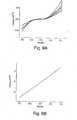
- the semiconductorcomprises a direct-band-gap semiconductor; a voltage is applied across a junction of two crossed semiconductors, each semiconductor having a smallest width of less than 500 nanometers; each semiconductor has a smallest width of less than 100 nanometers; a wavelength of the emitted light is controlled by controlling a dimension of the at least one semiconductor having a smallest width of less than 100 nanometers; the semiconductor is elongated, and a width of the elongated semiconductor is controlled; the semiconductor has a property that a mass of the semiconductor emits light at a first wavelength if the mass has a minimum shortest dimension, and the controlled dimension of the semiconductor is less than the minimum shortest dimension.
- a device having at least a doped semiconductor component and one or more other componentsis fabricated.
- a semiconductoris doped during its growth to produce the doped semiconductor component, and the doped semiconductor component is attached to at least one of the one or more other components.
- the doped semiconductoris at least one of the following: a single crystal, an elongated and bulk-doped semiconductor that, at any point along its longitudinal axis, has a largest cross-sectional dimension less than 500 nanometers, and a free-standing and bulk-doped semiconductor with at least one portion having a smallest width of less than 500 nanometers.
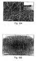
- the semiconductor componentis at least part of a nanowire; the semiconductor is doped during growth of the semiconductor.
- a process for controllably assembling a semiconductor device having elongated elements with a characteristic dimension in a transverse direction of the element on a nanometer scalecomprising: producing at least one first elements of a first doping type, orienting said first element in a first direction, and connecting said first element to at least one first contact to allow an electrical current to flow through the first element.
- the processfurther comprises producing at least one second elements of a second doping type, orienting said second element in a second direction different from the first direction, enabling an electrical contact between the first element and the second element, and connecting said second element to at least one second contact to allow an electrical current to flow between the first and second element;
- the processfurther comprises connecting said first element to spaced-apart contacts and arranging a gate electrode proximate to the first element between the spaced-apart contacts, thereby forming an FET;
- the first doping typeis one of n-type or p-type;
- the second doping typeis n-type if the first doping type is p-type, and p-type if the first doping type is n-type;
- the first elementis oriented by applying at least one of an electric field or a fluid flow;
- the first elementis suspended in the fluid flow;
- the first elementis oriented by applying a mechanical tool;
- the second elementis oriented by applying at least one of an electric field or
- a semiconductor devicecomprising: a silicon substrate having an array of metal contacts; a crossbar switch element formed in electrical communication with the array and having a first bar formed of a p-type semiconductor nanowire, and a second bar formed of an n-type semiconductor nanowire and being spaced away from the first bar and being disposed transversely thereto.
- the second baris spaces between 1-10 nm from the first bar.
- a method for manufacturing a nanowire semiconductor devicecomprising positioning a first nanowire between two contact points by applying a potential between the contact points; and positioning a second nanowire between two other contact points.
- a method for manufacturing a nanowire semiconductor devicecomprising forming a surface with one or more regions that selectively attract nanowires.
- a method for manufacturing a light-emitting diode from nanowiresthe diode having an emission wavelength determined by a dimension of a p-n junction between two doped nanowires.
- a method for manufacturing a semiconductor junctionby crossing a p-type nanowire and an n-type nanowire.
- a method of assembling one or more elongated structures on a surfacecomprising acts of: flowing a fluid that comprises the one or more elongated structures onto the surface; and aligning the one or more elongated structures on the surface to form an array of the elongated structures.
- flowingcomprises flowing the fluid in a first direction and aligning comprises aligning the one or more elongated structures as the fluid flows in the first direction to form a first layer of arrayed structures
- the methodfurther comprises changing a direction of the flow from the first direction to a second direction, and repeating the acts of flowing and aligning; at least a first elongated structure from the first layer contacts at least a second elongated structure from the second array; one of the first and second elongated structures is doped semiconductor of a first conductivity type and another of first and second elongated structures is doped semiconductor of a second conductivity type; the first conductivity type is p-type and the second conductivity type is n-type, and wherein the first and second elongated structures form a p-n junction; the surface is a surface of a substrate; the method further comprises transferring the array of elongated structures from the surface of the substrate to a surface of another substrate; transferring comprises stamping; the one or more e
- At least one of the elongated structuresare semiconductors; at least one of the elongated structures are doped semiconductors; at least one of the elongated structures are bulk-doped semiconductors; at least one of the structures is a doped single-crystal semiconductor; at least one of the structures is an elongated and bulk-doped semiconductor that, at any point along its longitudinal axis, has a largest cross-sectional dimension less than 500 nanometers; at least one of the structures is a free-standing and bulk-doped semiconductor with at least one portion having a smallest width of less than 500 nanometers; at least one of the structures is a doped semiconductor that is at least one of the following: a single crystal, an elongated and bulk-doped semiconductor that, at any point along its longitudinal axis, has a largest cross-sectional dimension less than 500 nanometers, and a free-standing and bulk-doped semiconductor with at least one portion having a smallest width of less than 500 nanometer
- a method of assembling one or more elongated structures on a surfacewherein one or more of the elongated structures are at least one of the following: a single crystal, an elongated and bulk-doped semiconductor that, at any point along its longitudinal axis, has a largest cross-sectional dimension less than 500 nanometers, and a free-standing and bulk-doped semiconductor with at least one portion having a smallest width of less than 500 nanometers, and wherein the method comprises acts of conditioning the surface with one or more functionalities that attract the one or more elongated structures to particular positions on the surface, and aligning the one or more elongated structures by attracting the one or more elongated structures to the particular positions using the one or more functionalities.
- the act of conditioningcomprises conditioning the surface with one or more molecules; the act of conditioning comprises conditioning the surface with one or more charges; the act of conditioning comprises conditioning the surface with one or more magnetos; the act of conditioning comprises conditioning the surface with one or more light intensities; conditioning the surface with one or more functionalities that attract the one or more elongated structures to particular positions on the surface using chemical force; the act of conditioning comprises conditioning the surface with one or more functionalities that attract the one or more elongated structures to particular positions on the surface using optical force; the act of conditioning comprises conditioning the surface with one or more functionalities that attract the one or more elongated structures to particular positions on the surface using electrostatic force; and/or the act of conditioning comprises conditioning the surface with one or more functionalities that attract the one or more elongated structures to particular positions on the surface using magnetic force.
- At least one of the elongated structuresare semiconductors; at least one of the elongated structures are doped semiconductors; at least one of the elongated structures are bulk-doped semiconductors; at least one of the structures is a doped single-crystal semiconductor; at least one of the structures is an elongated and bulk-doped semiconductor that, at any point along its longitudinal axis, has a largest cross-sectional dimension less than 500 nanometers; at least one of the structures is a free-standing and bulk-doped semiconductor with at least one portion having a smallest width of less than 500 nanometers; at least one of the structures is a doped semiconductor that is at least one of the following: a single crystal, an elongated and bulk-doped semiconductor that, at any point along its longitudinal axis, has a largest cross-sectional dimension less than 500 nanometers, and a free-standing and bulk-doped semiconductor with at least one portion having a smallest width of less than 500 nanometer
- a method of assembling a plurality of elongated structures on a surfacewherein one or more of the elongated structures are at least one of the following: a single crystal, an elongated and bulk-doped semiconductor that, at any point along its longitudinal axis, has a largest cross-sectional dimension less than 500 nanometers, and a free-standing and bulk-doped semiconductor with at least one portion having a smallest width of less than 500 nanometers, and wherein the method comprises acts of: depositing the plurality of elongated structures onto the surface; and electrically charging the surface to produce electrostatic forces between two or more of the plurality of the elongated structures.
- the electrostatic forcescause the two or more elongated structures to align themselves; the electrostatic forces cause the two or more elongated structures to align themselves into one or more patterns; and/or the one or more patterns comprise a parallel array.
- At least one of the elongated structuresare semiconductors; at least one of the elongated structures are doped semiconductors; at least one of the elongated structures are bulk-doped semiconductors; at least one of the structures is a doped single-crystal semiconductor; at least one of the structures is an elongated and bulk-doped semiconductor that, at any point along its longitudinal axis, has a largest cross-sectional dimension less than 500 nanometers; at least one of the structures is a free-standing and bulk-doped semiconductor with at least one portion having a smallest width of less than 500 nanometers; at least one of the structures is a doped semiconductor that is at least one of the following: a single crystal, an elongated and bulk-doped semiconductor that, at any point along its longitudinal axis, has a largest cross-sectional dimension less than 500 nanometers, and a free-standing and bulk-doped semiconductor with at least one portion having a smallest width of less than 500 nanometer
- a method of assembling a plurality of elongated structures on a surfacewherein one or more of the elongated structures are at least one of the following: a single crystal, an elongated and bulk-doped semiconductor that, at any point along its longitudinal axis, has a largest cross-sectional dimension less than 500 nanometers, and a free-standing and bulk-doped semiconductor with at least one portion having a smallest width of less than 500 nanometers, and wherein the method comprises acts of: dispersing the one or more elongated structures on a surface of a liquid phase to form a Langmuir-Blodgett film; compressing the Langmuir-Blodgett film; and transferring the compressed Langmuir-Blodgett film onto a surface.
- the surfaceis the surface of a substrate.
- At least one of the elongated structuresare semiconductors; at least one of the elongated structures are doped semiconductors; at least one of the elongated structures are bulk-doped semiconductors; at least one of the structures is a doped single-crystal semiconductor; at least one of the structures is an elongated and bulk-doped semiconductor that, at any point along its longitudinal axis, has a largest cross-sectional dimension less than 500 nanometers; at least one of the structures is a free-standing and bulk-doped semiconductor with at least one portion having a smallest width of less than 500 nanometers; at least one of the structures is a doped semiconductor that is at least one of the following: a single crystal, an elongated and bulk-doped semiconductor that, at any point along its longitudinal axis, has a largest cross-sectional dimension less than 500 nanometers, and a free-standing and bulk-doped semiconductor with at least one portion having a smallest width of less than 500 nanometer
- a method of assembling a plurality of one or more elongated structures on a surfacewherein at least one of the elongated structures are at least one of the following: a single crystal, an elongated and bulk-doped semiconductor that, at any point along its longitudinal axis, has a largest cross-sectional dimension less than 500 nanometers, and a free-standing and bulk-doped semiconductor with at least one portion having a smallest width of less than 500 nanometers, and wherein the method comprises acts of: dispersing the one or more elongated structures in a flexible matrix; stretching the flexible matrix in a direction to produce a shear force on the one or more elongated structures that causes the at least one elongated structure to align in the direction; removing the flexible matrix; and transferring the at least one aligned elongated structure to a surface.
- the directionis parallel to a plane of the surface
- the act of stretchingcomprises stretching the flexible matrix with an electrically-induced force
- the act of stretchingcomprises stretching the flexible matrix with an optically-induced force
- the act of stretchingcomprises stretching the flexible matrix with a mechanically-induced force
- the act of stretchingcomprises stretching the flexible matrix with a magnetically-induced force
- the surfaceis a surface of a substrate
- the flexible matrixis a polymer.
- At least one of the elongated structuresare semiconductors; at least one of the elongated structures are doped semiconductors; at least one of the elongated structures are bulk-doped semiconductors; at least one of the structures is a doped single-crystal semiconductor; at least one of the structures is an elongated and bulk-doped semiconductor that, at any point along its longitudinal axis, has a largest cross-sectional dimension less than 500 nanometers; at least one of the structures is a free-standing and bulk-doped semiconductor with at least one portion having a smallest width of less than 500 nanometers; at least one of the structures is a doped semiconductor that is at least one of the following: a single crystal, an elongated and bulk-doped semiconductor that, at any point along its longitudinal axis, has a largest cross-sectional dimension less than 500 nanometers, and a free-standing and bulk-doped semiconductor with at least one portion having a smallest width of less than 500 nanometer
- a system for growing a doped semiconductorcomprising: means for providing a molecules of the semiconductor and molecules of a dopant; and means for doping the molecules of the semiconductor with the molecules of the dopant during growth of the semiconductor to produce the doped semiconductor.
- At least one of the elongated structuresare semiconductors; at least one of the elongated structures are doped semiconductors; at least one of the elongated structures are bulk-doped semiconductors; at least one of the structures is a doped single-crystal semiconductor; at least one of the structures is an elongated and bulk-doped semiconductor that, at any point along its longitudinal axis, has a largest cross-sectional dimension less than 500 nanometers; at least one of the structures is a free-standing and bulk-doped semiconductor with at least one portion having a smallest width of less than 500 nanometers; at least one of the structures is a doped semiconductor that is at least one of the following: a single crystal, an elongated and bulk-doped semiconductor that, at any point along its longitudinal axis, has a largest cross-sectional dimension less than 500 nanometers, and a free-standing and bulk-doped semiconductor with at least one portion having a smallest width of less than 500 nanometer
- a system for assembling one or more elongated structures on a surfacecomprising: means for flowing a fluid that comprises the one or more elongated structures onto the surface; and means for aligning the one or more elongated structures on the surface to form an array of the elongated structures.
- At least one of the elongated structuresare semiconductors; at least one of the elongated structures are doped semiconductors; at least one of the elongated structures are bulk-doped semiconductors; at least one of the structures is a doped single-crystal semiconductor; at least one of the structures is an elongated and bulk-doped semiconductor that, at any point along its longitudinal axis, has a largest cross-sectional dimension less than 500 nanometers; at least one of the structures is a free-standing and bulk-doped semiconductor with at least one portion having a smallest width of less than 500 nanometers; at least one of the structures is a doped semiconductor that is at least one of the following: a single crystal, an elongated and bulk-doped semiconductor that, at any point along its longitudinal axis, has a largest cross-sectional dimension less than 500 nanometers, and a free-standing and bulk-doped semiconductor with at least one portion having a smallest width of less than 500 nanometer
- a system for assembling one or more elongated structures on a surfacewherein one or more of the elongated structures are at least one of the following: is at least one of the following: a single crystal, an elongated and bulk-doped semiconductor that, at any point along its longitudinal axis, has a largest cross-sectional dimension less than 500 nanometers, and a free-standing and bulk-doped semiconductor with at least one portion having a smallest width of less than 500 nanometers, and wherein the system comprises: means for conditioning the surface with one or more functionalities that attract the one or more elongated structures to particular positions on the surface, and means for aligning the one or more elongated structures by attracting the one or more elongated structures to the particular positions using the one or more functionalities.
- At least one of the elongated structuresare semiconductors; at least one of the elongated structures are doped semiconductors; at least one of the elongated structures are bulk-doped semiconductors; at least one of the structures is a doped single-crystal semiconductor; at least one of the structures is an elongated and bulk-doped semiconductor that, at any point along its longitudinal axis, has a largest cross-sectional dimension less than 500 nanometers; at least one of the structures is a free-standing and bulk-doped semiconductor with at least one portion having a smallest width of less than 500 nanometers; at least one of the structures is a doped semiconductor that is at least one of the following: a single crystal, an elongated and bulk-doped semiconductor that, at any point along its longitudinal axis, has a largest cross-sectional dimension less than 500 nanometers, and a free-standing and bulk-doped semiconductor with at least one portion having a smallest width of less than 500 nanometer
- a system for assembling a plurality of elongated structures on a surfacewherein one or more of the elongated structures are at least one of the following: is at least one of the following: a single crystal, an elongated and bulk-doped semiconductor that, at any point along its longitudinal axis, has a largest cross-sectional dimension less than 500 nanometers, and a free-standing and bulk-doped semiconductor with at least one portion having a smallest width of less than 500 nanometers, and wherein the system comprises means for depositing the plurality of elongated structures onto the surface; and means for electrically charging the surface to produce electrostatic forces between two or more of the plurality of the elongated structures.
- At least one of the elongated structuresare semiconductors; at least one of the elongated structures are doped semiconductors; at least one of the elongated structures are bulk-doped semiconductors; at least one of the structures is a doped single-crystal semiconductor; at least one of the structures is an elongated and bulk-doped semiconductor that, at any point along its longitudinal axis, has a largest cross-sectional dimension less than 500 nanometers; at least one of the structures is a free-standing and bulk-doped semiconductor with at least one portion having a smallest width of less than 500 nanometers; at least one of the structures is a doped semiconductor that is at least one of the following: a single crystal, an elongated and bulk-doped semiconductor that, at any point along its longitudinal axis, has a largest cross-sectional dimension less than 500 nanometers, and a free-standing and bulk-doped semiconductor with at least one portion having a smallest width of less than 500 nanometer
- a system for assembling a plurality of elongated structures on a surfacewherein one or more of the elongated structures are at least one of the following: is at least one of the following: a single crystal, an elongated and bulk-doped semiconductor that, at any point along its longitudinal axis, has a largest cross-sectional dimension less than 500 nanometers, and a free-standing and bulk-doped semiconductor with at least one portion having a smallest width of less than 500 nanometers, and wherein the system comprises: means for dispersing the one or more elongated structures on a surface of a liquid phase to form a Langmuir-Blodgett film; means for compressing the Langmuir-Blodgett film; and means for transferring the compressed Langmuir-Blodgett film onto a surface.
- At least one of the elongated structuresare semiconductors; at least one of the elongated structures are doped semiconductors; at least one of the elongated structures are bulk-doped semiconductors; at least one of the structures is a doped single-crystal semiconductor; at least one of the structures is an elongated and bulk-doped semiconductor that, at any point along its longitudinal axis, has a largest cross-sectional dimension less than 500 nanometers; at least one of the structures is a free-standing and bulk-doped semiconductor with at least one portion having a smallest width of less than 500 nanometers; at least one of the structures is a doped semiconductor that is at least one of the following: a single crystal, an elongated and bulk-doped semiconductor that, at any point along its longitudinal axis, has a largest cross-sectional dimension less than 500 nanometers, and a free-standing and bulk-doped semiconductor with at least one portion having a smallest width of less than 500 nanometer
- a system for assembling a plurality of one or more elongated structures on a surfacewherein at least one of the elongated structures are at least one of the following: a single crystal, an elongated and bulk-doped semiconductor that, at any point along its longitudinal axis, has a largest cross-sectional dimension less than 500 nanometers, and a free-standing and bulk-doped semiconductor with at least one portion having a smallest width of less than 500 nanometers, and wherein the system comprises: means for dispersing the one or more elongated structures in a flexible matrix; means for stretching the flexible matrix in a direction to produce a shear force on the one or more elongated structures that causes the at least one elongated structure to align in the direction; means for removing the flexible matrix; and means for transferring the at least one aligned elongated structure to a surface.
- At least one of the elongated structuresare semiconductors; at least one of the elongated structures are doped semiconductors; at least one of the elongated structures are bulk-doped semiconductors; at least one of the structures is a doped single-crystal semiconductor; at least one of the structures is an elongated and bulk-doped semiconductor that, at any point along its longitudinal axis, has a largest cross-sectional dimension less than 500 nanometers; at least one of the structures is a free-standing and bulk-doped semiconductor with at least one portion having a smallest width of less than 500 nanometers; at least one of the structures is a doped semiconductor that is at least one of the following: a single crystal, an elongated and bulk-doped semiconductor that, at any point along its longitudinal axis, has a largest cross-sectional dimension less than 500 nanometers, and a free-standing and bulk-doped semiconductor with at least one portion having a smallest width of less than 500 nanometer
- FIG. 1is a perspective view of an example of a semiconductor article, or nanowire, in accordance with an embodiment of the invention
- FIG. 2is a simplified schematic diagram of an example of a laser assisted catalytic growth process for fabrication of semiconductor nanowires
- FIG. 3is a schematic diagram that illustrates nanowire growth
- FIG. 4is a schematic diagram that illustrates an example of a method for controlling nanowire diameter
- FIG. 5is a schematic diagram that illustrates nanowire fabrication by deposition on the edge of surface steps
- FIG. 6is a schematic diagram that illustrates nanowire growth by vapor deposition in or on an elongated template
- FIGS. 7A-7Eillustrate orthogonal assembly of semiconductor nanowires to form devices
- FIGS. 8A-8Cshow silicon nanowire current as a function of bias voltage for different doping levels and gate voltages
- FIGS. 9A and 9Bshow silicon nanowire current as a function of bias voltage for different phosphorous doping levels and gate voltages
- FIGS. 10A and 10Bshow energy band diagrams for p-type and n-type silicon nanowire devices, respectively;
- FIGS. 11A and 11Bshow temperature dependent current-voltage curves recorded on a heavily boron doped silicon nanowire
- FIG. 12is a schematic diagram that depicts the use of monodispersed gold colloids as catalysts for the growth of well-defined GaP semiconductor nanowires;
- FIG. 13Ashows a FE-SEM image of nanowires synthesized from 28.2 nanometer colloids
- FIG. 13Bshows a TEM image of another wire in the sample
- FIGS. 14A-14Cshow histograms of measured diameters for wires grown from different diameter colloids
- FIG. 14Dshows a histogram of diameters for wires grown using the previous method without colloids, in which the laser is used to both generate the gold nanoclusters and the GaP reactants;
- FIG. 15shows a pseudobinary phase diagram for gold and gallium arsenide
- FIGS. 16A-16Cshow FE-SEM images of different nanowires prepared by laser assisted catalytic growth
- FIG. 17Ashows a diffraction contrast TEM image of an approximately 20 nanometer diameter gallium arsenide nanowire
- FIGS. 17B-17Dshow high resolution TEM images of different diameter nanowires
- FIG. 18Ashows a FE-SEM image of CdSe nanowires prepared by laser assisted catalytic growth
- FIG. 18Bshows a diffraction contrast TEM image of an 18 nanometer diameter CdSe nanowire
- FIG. 18Cshows a high resolution TEM image of an approximately 13 nanometer diameter CdSe nanowire
- FIG. 19is a schematic diagram showing GaN nanowire growth by laser assisted catalytic growth
- FIG. 20Ashows a FE-SEM image of bulk GaN nanowire synthesized by laser assisted catalytic growth
- FIG. 20Bshows a PXRD pattern recorded on bulk GaN nanowires
- FIG. 21Ashows a diffraction contrast TEM image of a GaN nanowire that terminates in a faceted nanoparticle of higher contrast
- FIG. 21Bshows an HRTEM image of another GaN nanowire with a diameter of approximately 10 nanometers
- FIGS. 22A-22Cillustrate doping and electrical transport of InP nanowires
- FIGS. 23A-23Dillustrate crossed nanowire junctions and electrical properties
- FIGS. 24A-24Dillustrate optoelectrical characterization of nanowire P—N junctions
- FIG. 25Ashows an EL image taken from a p-type Si and n-type GaN nanojunction
- FIG. 25Bshows current as a function of voltage for various gate voltages
- FIG. 25Cshows an EL spectrum for the nanojunction of FIGS. 25A ;
- FIGS. 26A-26Dillustrate parallel and orthogonal assembly of nanowires with electric fields
- FIGS. 27A-27Fillustrate crossed silicon nanowire junctions
- FIGS. 28A-28Dillustrate n + pn crossed silicon nanowire bipolar transistors
- FIGS. 29A-29Dillustrate complementary inverters and tunnel diodes
- FIGS. 30A and 30Bare schematics of fluidic channel structures for flow assembly
- FIGS. 31A-31Dillustrate parallel assembly of nanowire arrays
- FIGS. 32A-32Dillustrate assembly of periodic nanowire arrays
- FIGS. 33A-33Eillustrate layer-by-layer assembly and transport measurements of crossed nanowire arrays.
- the present inventionprovides, in one aspect, techniques for controlled doping of materials such as semiconductors at a very small spatial scale, and arrangement of doped materials in position relative to each other to create useful devices.
- One set of embodimentsinvolves doping of a semiconductor, with a dopant (e.g., boron, aluminum, phosphorous, arsenic, etc.) selected according to whether an n-type or p-type semiconductor is desired.
- a dopante.g., boron, aluminum, phosphorous, arsenic, etc.
- this inventioninvolves controlled doping of semiconductors selected from among indium phosphide, gallium arsenide, gallium nitride, cadmium selenide, and zinc selenide.
- Dopants including, but not limited to, zinc, cadmium, or magnesiumcan be used to form p-type semiconductors in this set of embodiments, and dopants including, but not limited to, tellurium, sulfur, selenium, or germanium can be used as dopants to form n-type semiconductors from these materials.
- These materialsdefine direct band gap semiconductor materials and these and doped silicon are well known to those of ordinary skill in the art.
- the present inventioncontemplates use of any doped silicon or direct band gap semiconductor materials for a variety of uses.
- a “width” of an articleis a distance of a straight line from a point on a perimeter of the article through the center of the article to another point on the perimeter of the article.
- a “width” or “cross-sectional dimension” at a point along the longitudinal axis of an elongated articleis a distance along a straight line that passes through the center of the cross-section at the point and that connects two points on the perimeter of the cross section.
- an “elongated” articlee.g., semiconductor or section thereof
- a ratio of the length of the article to the largest width at the pointis greater than 2:1.
- the “longitudinal axis” of an elongated articleis an axis along a largest dimension of the article.
- the “length” of an elongated articleis a distance along the longitudinal axis from end to end of the article.
- a “longitudinal section” of an elongated articleis a portion of the elongated article along the longitudinal axis of the elongated article than can have any length greater than zero and less than or equal to the length of the article.
- a “cross-section” at a point along the longitudinal axis of an elongated articleis a plane at the point across the elongated article that is orthogonal to the longitudinal axis of the article.
- a “cylindrical” articleis an article having an exterior shaped like a cylinder, but does not define or reflect any properties regarding the interior of the article.
- a cylindrical articlemay have a solid interior or may have a hollowed-out interior.
- a “nanowire” or “NW”is an elongated semiconductor, i.e., a nanoscale semiconductor, that at any point along its length has at least one cross-sectional dimension and, in some embodiments, two orthogonal cross-sectional dimensions less than 500 nanometers, preferably less than 200 nanometers, more preferably less than 150 nanometers, still more preferably less than 100 nanometers, even more preferably less than 70, still more preferably less than 50 nanometers, even more preferably less than 20 nanometers, still more preferably less than 10 nanometers, and even less than 5 nanometers.
- the cross-section of the elongated semiconductormay have any arbitrary shape, including, but not limited to, circular, square, rectangular, elliptical. Regular and irregular shapes are included.
- NTnanotube
- NTis a nanowire that has a hollowed-out core.
- a “bulk-doped” articleis an article for which a dopant is incorporated substantially throughout the crystalline lattice of the article, as opposed to an article in which a dopant is only incorporated in particular regions.
- some articlessuch as carbon NTs typically are doped after the base material is grown, and thus the dopant only extends a finite distance from the surface or exterior of the carbon NT into the interior of the crystal line lattice.
- carbon NTsare often combined as nested tubes forming alternating layers of base material and doped base material such that the dopant is not incorporated throughout the crystal line lattice of the base material.
- nanowireAs used herein to describe a “nanowire” or “NW”, “doped” means bulk-doped. Accordingly, as used herein, a “doped nanowire” or “doped NW” is a bulk-doped nanowire
- an “array” of articlescomprises a plurality of the articles.
- a “crossed array”is an array where at least one of the articles contacts either another of the articles or a signal node (e.g., an electrode).
- a first articlee.g., a nanowire or larger-sized structure “coupled” to a second article is disposed such that the first article either physically contacts the second article or is proximate enough to the second article to influence a property (e.g., electrical property, optical property, magnetic property) of the second article.
- a propertye.g., electrical property, optical property, magnetic property
- the present inventioncontemplates, in one aspect, an elongated semiconductor that has a smallest width of less than 500 nanometers that is doped in any way (n-type or p-type).
- the semiconductormay have a smallest width less than about 200 nanometers, less than about 150 nanometers, or less than about 100 nanometers.
- the semiconductorhas a smallest width of less than about 80 nanometers, more preferably less than about 70 nanometers, preferably less than about 50 nanometers. Smaller widths, such as those with at least one dimension of less than about 20 nanometers, less than about 10 nanometers, or less than about 5 nanometers also are included.
- two orthogonal cross-sectional dimensions of the elongated semiconductormay be less than the values given above.
- the aspect ratioi.e., the ratio of semiconductor length to largest width, is greater than 2:1. In other embodiments, the aspect ratio may be greater than 4:1, greater than 10:1, greater than 100:1 or even greater than 1000:1. Semiconductors such as these, at very small dimensions, find a variety of uses as described below.
- FIG. 1is a perspective diagram illustrating an example of a cylindrical semiconductor L 1 , for example, a wire-like semiconductor such as a nanowire.
- the cylindrical semiconductor L 1has a length L 2 and a longitudinal axis L 3 .
- the cylindrical semiconductor L 1has a plurality of widths L 4 across cross-section L 6 , where one of the widths L 4 is a smallest width at the point L 5 .
- Such semiconductorsmay be free-standing.
- a “free-standing” articleis an article that at some point in its life is not attached to another article or that is in solution.
- such a semiconductormay be a bulk-doped semiconductor.
- a “bulk-doped semiconductor” articlee.g. article or section of an article
- NTstypically are doped after the semiconductor is grown, and thus the dopant only extends a finite distance from the surface or exterior of the nanotube into the interior of the crystalline lattice.
- NTsare often combined as nested tubes (i.e.
- cylindersforming alternating layers of semiconductor and doped semiconductor such that the dopant is not incorporated throughout the crystalline lattice of the semiconductor.
- dopantis not incorporated throughout the crystalline lattice of the semiconductor.
- the semiconductormay be doped during growth of the semiconductor. Doping the semiconductor during growth may result in the property that the doped semiconductor is bulk-doped. Further, such doped semiconductors may be controllably doped, such that a concentration of a dopant within the doped semiconductor can be controlled and therefore reproduced consistently, making possible the commercial production of such semiconductors.
- a variety of devicesmay be fabricated using semiconductors such as those described above. Such devices include electrical devices, optical devices, mechanical devices or any combination thereof, including opto-electronic devices and electromechanical devices.
- a field effect transistoris produced using a doped semiconductor having a smallest width of less than 500 nanometers or other width described above.
- the doped semiconductorcan be either a p-type or n-type semiconductor, as is known by those of ordinary skill in the art in FET fabrication. While FETs are known using nanotubes, to the inventors' knowledge, prior arrangements select nanotubes at random, without control over whether the nanotube is metallic or semiconducting. In such a case a very low percentage of devices are functional, perhaps less than one in twenty, or one in fifty, or perhaps approximately one in one hundred.
- the present inventioncontemplates controlled doping of nanowires such that a fabrication process can involve fabricating functional FETs according to a technique in which much greater than one in fifty devices is functional.
- the techniquecan involve doping a nanowire, then fabricating an FET therefrom.
- the inventionalso provides lightly-doped complementary inverters (complementary metal oxide semiconductors) arranged simply by contact of an n-type semiconductor with a p-type semiconductor, for example by arrangement of crossed n-type and p-type semiconducting nanowires as shown below.
- lightly-doped complementary inverterscomplementary metal oxide semiconductors
- tunnel diodeswith heavily-doped semiconducting components.
- a tunnel diodecan be arranged similarly or exactly the same as a complementary inverter, with the semiconductors being heavily doped rather than lightly doped. “Heavily doped” and “lightly doped” are terms the meaning of which is clearly understood by those of ordinary skill in the art.
- One important aspect of the present inventionis the ability to fabricate essentially any electronic device that can benefit from adjacent n-type and p-type semiconducting components, where the components are pre-fabricated (doped, in individual and separate processes with components separate from each other when doped) and then brought into contact after doping.
- Thisis in contrast to typical prior art arrangements in which a single semiconductor is n-doped in one region and p-doped in an adjacent region, but the n-type semiconductor region and p-type semiconducting regions are initially adjacent prior to doping and do not move relative to each other prior to or after doping. That is, n-type and p-type semiconductors, initially in non-contacting arrangement, are brought into contact with each other to form a useful electronic device.
- any devicecan be made in accordance with this aspect of the invention that one of ordinary skill in the art would desirably make using n-type and p-type semiconductors in combination.
- Examples of such devicesinclude, but are not limited to, field effect transistors (FETs), bipolar junction transistors (BJTs), tunnel diodes, complementary inverters, light emitting devices, light sensing devices, gates, inverters, AND, NAND, OR, and NOR gates, latches, flip-flops, registers, switches, clock circuitry, static or dynamic memory devices and arrays, state machines, gate arrays, and any other dynamic or sequential logic or other digital devices including programmable circuits.
- analog devices and circuitryincluding but not limited to, amplifiers, switches and other analog circuitry using active transistor devices, as well as mixed signal devices and signal processing circuitry.
- Electronic devices incorporating semiconductor nanowirescan be controlled, for example, by electrical, optical or magnetic signals.
- the controlmay involve switching between two or more discrete states or may involve continuous control of nanowire current, i.e., analog control.
- the devicesmay be controlled as follows:
- crossed p/n junctionswhich can be junctions of crossed n-type and p-type nanowires.
- Crossed p/n junctionsare defined by at least one n-type semiconductor and at least one p-type semiconductor, at least one portion of each material contacting at least one portion of the other material, and each semiconductor including portions that do not contact the other component. They can be arranged by pre-doping the nanowires, then bringing them into proximity with each other using techniques described below.
- Light-emission sourcesare provided in accordance with the invention as well, in which electrons and holes combine, emitting light.
- One type of light-emission source of the inventionincludes at least one crossed p/n junction, in particular, crossed p-type and n-type nanowires. In this and other arrangements of the invention using crossed nanowires, the wires need not be perpendicular, but can be.
- forward biasedpositive charge applied to the p-type wire and a negative charge applied to the n-type wire
- electronsflow toward the junction in the n-type wire and holes flow toward the junction in the p-type wire.
- holes and electronscombine, emitting light.
- Other techniquesmay be used to cause one or more nanowires, or other semiconductors to emit light, as described below in more detail.
- the wavelength of light emissioncan be controlled by controlling the size of at least one, and preferably both components that are crossed to form the light-emitting junction. For example, where nanowires are used, a nanowire with larger smallest dimension (broader wire) will provide emission at a lower frequency. For example, in the case of indium phosphide, at size scales associated with typical fabrication processes, the material emits at 920 nanometers. At the size scales of the present invention the wavelength of emission can be controlled to be at wavelengths shorter than 920 nanometers, for example between 920 and 580 nanometers. Wavelengths can be selected within this range, such as 900, 850, 800, 750, 700 nanometers, etc., depending upon wire size.
- one aspect of the inventioninvolves a semiconductor light-emission source that emits at a higher frequency than the semiconductor causing emission emits in its bulk state such increase of the frequency of emission of light is often referred to herein as quantum confinement.
- “Bulk state”, in this context,means a state in which it is present as a component, or a portion of a component having a smallest dimension of greater than 500 nanometers. “Bulk state” also can be defined as that state causing a material's inherent wavelength or frequency of emission. The present invention provides for such control over emission frequency of essentially any semiconducting or doped semiconducting material.
- Assembly, or controlled placement of nanowires on surfacescan be carried out by aligning nanowires using an electrical field.
- An electrical fieldis generated between electrodes, nanowires are positioned between the electrodes (optionally flowed into a region between the electrodes in a suspending fluid), and will align in the electrical field and thereby can be made to span the distance between and contact each of the electrodes.
- individual contact pointsare arranged in opposing relation to each other, the individual contact points being tapered to form a point directed towards each other.
- An electric field generated between such pointswill attract a single nanowire spanning the distance between, and contacting each of, the electrodes.
- individual nanowirescan readily be assembled between individual pairs of electrical contacts.
- Crossed-wire arrangementsincluding multiple crossings (multiple parallel wires in a first direction crossed by multiple parallel wires in a perpendicular or approximately perpendicular second direction) can readily be formed by first positioning contact points (electrodes) at locations where opposite ends of the crossed wires desirably will lie. Electrodes, or contact points, can be fabricated via typical microfabrication techniques.
- a nanowire solutioncan be prepared as follows. After nanowires are synthesized, they are transferred into a solvent (e.g., ethanol), and then are sonicated for several seconds to several minutes to obtain a stable suspension.
- a solvente.g., ethanol
- Another arrangementinvolves forming surfaces including regions that selectively attract nanowires surrounded by regions that do not selectively attract them.
- —NH 2can be presented in a particular pattern at a surface, and that pattern will attract nanowires or nanotubes having surface functionality attractive to amines.
- Surfacescan be patterned using known techniques such as electron-beam patterning, “soft-lithography” such as that described in International Patent Publication No. WO 96/29629, published Jul. 26, 1996, or U.S. Pat. No. 5,512,131, issued Apr. 30, 1996, each of which is incorporated herein by reference. Additional techniques are described in U.S. patent application Ser. No. 60/142,216, filed Jul. 2, 1999, by Lieber, et al., incorporated herein by reference.
- Fluid flow channelscan be created at a size scale advantageous for placement of nanowires on surfaces using a variety of techniques such as those described in International Patent Publication No. WO 97/33737, published Sep. 18, 1997, and incorporated herein by reference. Other techniques include those described in U.S. patent application Ser. No. 09/578,589, filed May 25, 2000, and incorporated herein by reference.
- FIGS. 7A-7Eshow one such technique for creating a fluid flow channel using a polydimethyl siloxane (PDMS) mold.
- Channelscan be created and applied to a surface, and a mold can be removed and re-applied in a different orientation to provide a cross flow arrangement or different arrangement.
- PDMSpolydimethyl siloxane
- the flow channel arrangementcan include channels having a smallest width of less than 1 millimeter, preferably less than 0.5 millimeter, 200 microns or less. Such channels are easily made by fabricating a master by using photolithography and casting PDMS on the master, as described in the above-referenced patent applications and international publications. Larger-scale assembly is possible as well. The area that can be patterned with nanowire arrays is defined only by the feature of the channel which can be as large as desired.
- Semiconductor nanowireshave a crystalline core sheathed with 1-10 nm thick of amorphous oxide. This allows surface modification to terminate the surface with various functional groups.
- alkyloxysilane groupe.g. —Si(OCH 3 )
- reacting with nanowire surfacethe other end of which comprise (1) —CH 3 , —COOH, —NH 2 , —SH, —OH, hydrazide, and aldehyde groups; (2) light activatable moieties: aryl azide, fluorinated aryl azide, benzophenone etc.
- the substrate and electrodesare also modified with certain functional groups to allow nanowires to specifically bind or not bind onto the substrate/electrodes surface based on the their interaction.
- Surface-functionalized nanowirescan also be coupled to the substrate surface with functional cross-linkers, e.g. (1) Homobifunctional cross-linkers, comprising homobifunctional NHS esters, homobifunctional imidoesters, homobifunctional sulfhydryl-reactive linkers, difluorobenzene derivatives, homobifunctional photoactive linkers, homobifunctional aldehyde, bis-epoxides, homobifunctional hydrazide etc. (2) Heterobifunctional cross-linkers (3) Trifunctional cross-linkers.
- functional cross-linkerse.g.
- Homobifunctional cross-linkerscomprising homobifunctional NHS esters, homobifunctional imidoesters, homobifunctional sulfhydryl-reactive linkers, difluorobenzene derivatives, homobifunctional photoactive linkers, homobifunctional aldehyde, bis-epoxides, homobifunctional hydrazide etc.
- the assembly of nanowires onto substrate and electrodescan also be assisted using bimolecular recognition.
- Some good bio-recognitionsare: DNA hybridization, antibody-antigen binding, biotin-avidin (or streptavidin) binding.
- SiNWselongated nanoscale semiconductors
- LCGlaser assisted catalytic growth
- a composite targetthat is composed of a desired material (e.g. InP) and a catalytic material (e.g. Au) creates a hot, dense vapor which quickly condenses into liquid nanoclusters through collision with the buffer gas. Growth begins when the liquid nanoclusters become supersaturated with the desired phase and continues as long as the reactant is available. Growth terminates when the nanowires pass out of the hot reaction zone or when the temperature is turned down.
- Auis generally used as catalyst for growing a wide range of elongated nanoscale semiconductors.
- the catalystis not limited to Au only.
- a wide rage of materialssuch as (Ag, Cu, Zn, Cd, Fe, Ni, Co . . . ) can be used as the catalyst.
- any metal that can form an alloy with the desired semiconductor material, but doesn't form more stable compound than with the elements of the desired semiconductorcan be used as the catalyst.
- the buffer gascan be Ar, N 2 , and others inert gases. Sometimes, a mixture of H 2 and buffer gas is used to avoid un-desired oxidation by residue oxygen. Reactive gas can also be introduced when desired (e.g. ammonia for GaN). The key point of this process is laser ablation generates liquid nanoclusters that subsequently define the size and direct the growth direction of the crystalline nanowires.
- the diameters of the resulting nanowiresare determined by the size of the catalyst cluster, which in turn can be varied by controlling the growth conditions (e.g. background pressure, temperature, flow rate . . . ). For example, lower pressure generally produces nanowires with smaller diameters. Further diameter control can be done by using uniform diameter catalytic clusters.
- nanowires with uniform size (diameter) distributioncan be produced, where the diameter of the nanowires is determined by the size of the catalytic clusters, as illustrated in FIG. 4 .
- the growth timenanowires with different lengths can be grown.
- nanowirescan be flexibly doped by introducing one or more dopants into the composite target (e.g. (Ge for n-type doping of InP).
- the doping concentrationcan be controlled by controlling the relative amount of doping element, typically 0-20%, introduced in the composite target.
- Laser ablationmay be used as the way to generate the catalytic clusters and vapor phase reactant for growth of nanowires and other related elongated nanoscale structures. but fabrication is not limited to laser ablation. Many ways can be used to generate vapor phase and catalytic clusters for nariowire growth (e.g. thermal evaporation).
- C-CVDcatalytic chemical vapor deposition
- nanowirescan be doped by introducing the doping element into the vapor phase reactant (e.g. diborane and phosphane for p-type and n-type doped nanowire).
- the doping concentrationcan be controlled by controlling the relative amount of the doping element introduced in the composite target. It is not necessary to obtain elongated nanoscale semiconductors with the same doping ratio as that in the gas reactant. However, by controlling the growth conditions (e.g. temperature, pressure . . . ), nanowires with same doping concentration can be reproduced. And the doping concentration can be varied over a large range by simply varying the ratio of gas reactant (e.g. 1 ppm-10%).
- nanowires of any of a variety of materialscan be grown directly from vapor phase through a vapor-solid process.
- nanowirescan also be produced by deposition on the edge of surface steps, or other types of patterned surfaces, as shown in FIG. 5 .
- nanowirescan be grown by vapor deposition in/on any general elongated template, for example, as shown in FIG. 6 .
- the porous membranecan be porous silicon, anodic alumina or diblock copolymer and any other similar structure.
- the natural fibercan be DNA molecules, protein molecules carbon nanotubes, any other elongated structures.
- the source materialscan be came from a solution phase rather than a vapor phase. While in solution phase, the template can also be column micelles formed by surfactant molecules in addition to the templates described above.
- elongated nanoscale semiconductorsincluding semiconductor nanowires and doped semiconductor nanowires
- Such bulk-doped semiconductorsmay include various combinations of materials, including semiconductors and dopants. The following are non-comprehensive lists of such materials. Other materials may be used. Such materials include, but are not limited to:
- BN/BP/BAsAlN/AlP/AlAs/AlSb, GaN/GaP/GaAs/GaSb, InN/InP/InAs/InSb,
- any combination of two or more of the above compounde.g.: AlGaN, GaPAs, InPAs, GaInN, AlGaInN, GaInAsP . . . )
- ZnO/ZnS/ZnSe/ZnTeCdS/CdSe/CdTe, HgS/HgSe/HgTe, BeS/BeSe/BeTe/MgS/MgSe
- any combination of two or more of the above compounde.g.: (ZnCd)Se, Zn(SSe) . . . )
- II-IV-V 2BeSiN 2 , CaCN 2 , ZnGeP 2 , CdSnAs 2 , ZnSnSb 2 . . .
- I-IV 2 -V 3CuGeP 3 , CuSi 2 P 3 . . .
- I-III-VI 2(Cu, Ag)(Al, Ga, In, Tl, Fe)(S, Se, Te) 2
- IV 3 -V 4Si 3 N 4 , Ge 3 N 4 . . .
- III 2 -VI 3Al 2 O 3 , (Al, Ga, In) 2 (S, Se, Te) 3 . . .
- III 2 -IV-VIAl 2 CO . . .
- a p-type dopantmay be selected from Group III, and an n-type dopant may be selected from Group V.
- a p-type dopantmay be selected from the group consisting of B, Al and In, and an n-type dopant may be selected from the group consisting of P, As and Sb.
- a p-type dopantmay be selected from Group II, including Mg, Zn, Cd and Hg, or Group IV, including C and Si.
- An n-type dopantmay be selected from the group consisting of Si, Ge, Sn, S, Se and Te. It will be understood that the invention is not limited to these dopants.
- Single crystal n-type and p-type silicon nanowireshave been prepared and characterized by electrical transport measurements.
- a “single crystal” itemis an item that has covalent bonding, ionic bonding, or a combination thereof throughout the item. Such a single crystal item may include defects in the crystal, but is distinguished from an item that includes one or more crystals, not ionically or covalently bonded, but merely in close proximity to one another.
- Laser catalytic growthwas used to introduce controllably either boron or phosphorous dopants during the vapor phase growth of SiNWs.
- SiNWswere synthesized using the laser-assisted catalytic growth (LCG) we have described previously. Briefly, a Nd-YAG laser (532 nm; 8 ns pulse width, 300 mJ/pulse, 10 Hz) may be used to ablate a gold target, which produces gold nanocluster catalyst particles within a reactor.
- the SiNWsmay be grown in a flow of SiH 4 as the reactant.
- Such SiNWsmay be doped with boron by incorporating B 2 H 6 in the reactant flow, and may be doped with phosphorous using a Au-P target (99.5:0.5 wt %, Alfa Aesar) and additional red phosphorous (99%, Alfa Aesar) at the reactant gas inlet.
- Transmission electron microscopy (TEM) measurementsdemonstrate that doped SiNWs grown using this technique have a single crystal silicon core that is covered by a dense SiO x sheath as described previously.
- SiNWsElectrical contact to individual SiNWs were made using standard electron beam lithography methods using a JEOL 6400 writer.
- the nanowireswere supported on oxidized Si substrate (1-10 ⁇ -cm resistivity, 600 nm SiO 2 , Silicon Sense, Inc.) with the underlying conducting Si used as a back gate.
- the contacts to the SiNWswere made using thermally evaporated Al (50 nm) and Au (150 nm). Electrical transport measurements were made using a homebuilt system with less than or equal to 1 pA noise under computer control. The temperature-dependent measurements were made in a Quantum Design magnetic property measurement system.
- TEM studiesshow that the boron and phosphorous-doped SiNWs are single crystals, although these measurements do not have sufficient sensitivity to quantify the boron or phosphorous doping level in individual wires.
- a gate electrodeis used to vary the electrostatic potential of the SiNW while measuring current versus voltage of the nanowire.
- the change in conductance of SiNWs as function of gate voltagecan be used to distinguish whether a given nanowire is p-type or n-type since the conductance will vary oppositely for increasing positive (negative) gate voltages.
- FIGS. 8A-8CTypical gate-dependent current versus bias voltage (I-V) curves recorded on intrinsic and B-doped SiNWs are shown in FIGS. 8A-8C .
- the two B-doped wires shown in FIGS. 8B and 8Cwere synthesized using SiH 4 : B 2 H 6 ratios of 1000:1 and 2:1, respectively.
- the two terminal I-V curvesare linear and thus suggest that the metal electrodes make ohmic contacts to the SiNWs.
- the small nonlinearity observed in the intrinsic nanowireindicates that this contact is slightly nonohmic.
- This wirehas a very low resistivity of 6.9 ⁇ 10 ⁇ 3 ⁇ -cm and shows no dependence on V g ; that is, I-V data recorded with V g of 0 and 20 V are overlapping. These results are consistent with a high carrier concentration that is near the metallic limit.
- V g -dependent transport in lightly and heavily P-doped SiNWsWe have also measured V g -dependent transport in lightly and heavily P-doped SiNWs.
- the I-V recorded on the lightly doped nanowire( FIG. 9A ) is somewhat nonlinear, which indicates nonideal contact between the electrodes and nanowire, and the V g dependence is opposite of that observed for the B-doped SiNWs.
- this observed gate dependenceis consistent with n-type material as expected for P-doping.
- heavily P-doped SiNWshave also been made and studied.
- the I-V data recorded on a typical heavily P-doped wireare linear, have a resistivity of 2.3 ⁇ 10 2 ⁇ -cm, and shows no dependence on V g .
- the low resistivity (four orders of magnitude smaller than the lightly P-doped sample) and V g independencedemonstrate that high carrier concentrations can also be created via P-doping of the SiNWs.
- a p-type nanowire (a) and n-type nanowire (b)are contacted at both ends to metal electrodes.
- the SiNW bandsbend (up for p-type; down for n-type) to bring the nanowire Fermi level in line with that of the metal contacts.
- V g >0the bands are lowered, which depletes the holes in B-doped SiNWs and suppress conductivity, but leads to an accumulation of electrons in P-doped SiNWs and enhance the conductivity.
- V g ⁇ 0will raise the bands and increase the conductivity of B-doped (p-type) SiNWs and decrease the conductivity of the P-doped (n-type) nanowires.
- the slopes of dI/dV g for the intrinsic (2.13 ⁇ 10 ⁇ 11 ) and B-doped (9.54 ⁇ 10 ⁇ 9 ) SiNWyield mobilities of 5.9 ⁇ 10 ⁇ 3 cm 2 /V-s and 3.17 cm 2 /V-s, respectively.
- the mobility for the B-doped nanowireis comparable to that expected in bulk Si at a doping concentration of 10 20 cm ⁇ 3 .
- the mobilityis expected to increase with decreasing dopant concentration, although in our intrinsic (low dopant concentration) SiNW the mobility is extremely low. It is possible that the reduced mobility is due to enhanced scattering in the smaller diameter (intrinsic) SiNW. We believe that future studies of the mobility as a function of diameter (for constant dopant concentration) should illuminate this important point.
- Single crystal n-type and p-type silicon nanowireshave been prepared and characterized by electrical transport measurements.
- Laser catalytic growthwas used to introduce controllably either boron or phosphorous dopants during the vapor phase growth of SiNWs.
- Two-terminal, gate-dependent measurements made on individual boron-doped and phosphorous-doped SiNWsshow that these materials behave as p-type and n-type materials, respectively.
- Estimates of the carrier mobility made from gate-dependent transport measurementsare consistent with diffusive transport, and show an indication for reduced mobility in smaller diameter wires.
- these studiesshow it is possible to incorporate high dopant concentrations in the SiNWs and approach the metallic regime.
- Temperature-dependent measurements made on heavily doped SiNWsshow no evidence for single electron charging at temperatures down to 4.2 K, and thus suggest that the SiNWs possess a high degree of structural and doping uniformity.
- Crossed SiNW p-n junctionshave been formed by directed assembly of p-type (n-type) SiNWs over n-type (p-type) SiNWs.
- Transport measurementsexhibit rectification in reverse bias and a sharp current onset in forward bias.
- Simultaneous measurements made on the p-type and n-type SiNWs making up the junctiondemonstrate that the contacts to these nanowires are ohmic (nonrectifying), and thus that the rectifying behavior is due to the p-n junction between the two SiNWs.
- FIG. 8Ashows current (I) vs bias voltage (V) curves recorded on a 70 nm diameter intrinsic SiNW at different gate voltages (V g ).
- FIG. 10Ashows energy band diagrams for p-type SiNW devices.
- FIG. 10Bshows energy band diagrams for n-type SiNW devices. The diagrams show schematically the effect of V g on the electrostatic potential for both types of nanowires.
- FIGS. 11A and 11Bshow temperature dependent I-V curves recorded on a heavily B-doped SiNW.
- curves 1 , 2 , 3 , 4 , 5 , and 6correspond to temperatures of 295, 250, 200, 150, 100, and 50 K, respectively.
- FIG. 11Bshows I-V data recorded on the nanowire at 4.2 K.
- High-resolution TEMshows that the wires are a single crystal zinc blend with a [111] growth direction, and energy dispersive X-ray analysis confirms that the nanowire composition is stoichiometric GaP.
- monodisperse nanocluster catalysts combined with the LCG methodwill enable the growth of a wide range of semiconductor nanowires with well-defined and controlled diameters, and thus opens up opportunities from fundamental properties of one-dimensional (1D) systems to the assembly of functional nanodevices.
- T-wireshave been fabricated by growing semiconductor quantum wells via molecular beam epitaxy, followed by cleavage and overgrowth on the cleaved surface, while “V-groove” nanowires have been prepared by etching trenches on a surface and then depositing a small amount of material into the resulting grooves.
- V-groove nanowireshave been prepared by etching trenches on a surface and then depositing a small amount of material into the resulting grooves.
- One of the significant limitations of these approachesis that the nanowires are embedded in a substrate, which precludes the assembly of complex 2D and 3D nanostructures.
- Template approacheshave also been used for growing a wide-range of nanowires. These methods can provide good control over the length and diameter of nanowires, although they are limited in that polycrystalline structures are often produced.
- GaP nanowireswere grown by LCG using 8.4, 18.5, and 28.2 nm diameter gold colloids.
- the catalyst nanoclustersare supported on a SiO 2 substrate and laser ablation is used to generate the Ga and P reactants from a solid target of GaP.
- Field emission scanning electron microscopydemonstrates that nanowires with lengths exceeding 10 ⁇ m ( FIG. 1 3 A) were obtained using all three sizes of catalyst. Examination of the nanowire ends also shows the presence of the nanocluster catalyst ( FIG. 1 3 A, inset). Control experiments carried out without the Au colloids did not produce nanowires.
- the FESEM imagesshow that the nanowire diameter distributions are narrower than obtained in experiments without the colloid catalysts, although FESEM is not a good method for quantifying these distributions since small variations in the focal plane can produce significant changes in the observed diameter.
- Substrateswere made by placing a silicon wafer with 600 nm of thermal oxide (Silicon Sense) into a solution of 95:5 EtOH:H 2 O with 0.4% N-[3-(Trimethoxysilyl)propyl]-ethylenediamine for 5 minutes, followed by curing at 100-110° C. for 10 minutes. Solutions of Au colloids (Ted Pella) were diluted to concentrations of 10 9 -10 11 particles/mL to minimize aggregation and were deposited on the substrates. Substrates were placed in a quartz tube at the downstream end of the furnace with a solid target of GaP placed 3-4 cm outside of the furnace at the upstream end.
- the chamberwas evacuated to less than 100 mTorr, and then maintained at 250 Torr with an Airflow of 100 sccm.
- the substrateswere examined by FESEM (LEO 982).
- FESEMLEO 982
- TEMJEOL 200CX and 2010
- EDAX analysisnanowires were deposited onto copper grids after removal from the substrates by sonication in ethanol.
- FIG. 12is a schematic depicting the use of monodisperse gold colloids as catalysts for the growth of well-defined GaP semiconductor nanowires.
- FIG. 13Ashows a FESEM image of nanowires synthesized from 28.2 nm colloids (scale bar is 5 ⁇ m).
- the insetis a TEM image of the end of one of these wires (scale bar is 50 nm).
- the high contrast featurecorresponds to the colloid catalyst at the end of the wire.
- FIG. 13Bshows a TEM image of another wire in this sample (scale bar is 10 nm).
- the [111] lattice planesare resolved, showing that wire growth occurs along this axis, in agreement with earlier work. Measurement of the inter-plane spacing gives a lattice constant of 0.54 nm ( ⁇ 0.05 nm) for the wire, in agreement with the bulk value for GaP, 0.5451 nm.
- FIGS. 14A-14Cshow histograms of measured diameters for wires grown from 28.2 nm ( FIG. 14A ), 18.5 nm ( FIG. 14B ), and 8.4 nm ( FIG. 14C ) colloids.
- the solid lineshows the distribution of wire.
- FIG. 14Dshows a histogram of diameters for wires grown using the previous method without colloids, in which the laser is used to both generate the Au nanoclusters and the GaP reactants.
- the distributionis very broad (stan. dev. 23.9 nm) and the mean diameter (42.7 nm) greater than those synthesized using the predefined colloid catalyst.
- the reported nanowire diameterscorrespond to the crystalline cores.
- the amorphous oxide layers on the surface of all nanowiresare relatively uniform from wire to wire within the same experiment, but vary from 2-6 nm in thickness between syntheses.
- Nanowires of binary group III-V materialsGaAs, GaP, InAs and InP
- ternary III-V materialsGaAs/P, InAs/P
- binary II-VI compoundsZnS, ZnSe, CdS, and CdSe
- binary SiGe alloyshave been prepared in bulk quantities as high purity (>90%) single crystals.
- the nanowireshave diameters varying from three to tens of nanometers, and lengths extending to tens of micrometers. The synthesis of this wide range of technologically important semiconductor nanowires can be extended to many other materials and opens up significant opportunities in nanoscale science and technology.
- Nanowires and nanotubeshave been the focus of considerable attention, because they have the potential to answer fundamental questions about one-dimensional systems and are expected to play a central role in applications ranging from molecular electronics to novel scanning microscopy probes.
- To explore such diverse and exciting opportunitiesrequires nanowire materials for which the chemical composition and diameter can be varied.
- considerable efforthas been placed on the bulk synthesis of nanowires, and while advances have been made using template, laser ablation, solution, and other methods, in no case has it been demonstrated that one approach could be exploited in a predictive manner to synthesize a wide range of nanowire materials.
- LCGlaser-assisted catalytic growth
- semiconductor nanowires of the III-V materials GaAs, GaP, GaAsP, InAs, InP and InAsP, the II-VI materials ZnS, ZnSe, CdS and CdSe, and IV-IV alloys of SiGecan be synthesized in high yield and purity using this approach.
- Compound semiconductors, such as GaAs and CdSe,are especially interesting targets since their direct band gaps give rise to attractive optical and electrooptical properties.
- the nanowireshave been prepared as single crystals with diameters as small as 3 nm, which places them in a regime of strong radial quantum confinement, and lengths exceeding 10 ⁇ m.
- the prediction of growth conditions for binary and more complex nanowires using the LCG methodis, in principle, significantly more difficult than previous studies of elemental Si and Ge nanowires due to the complexity of ternary and higher order phase diagrams.
- this complexitycan be greatly reduced by considering pseudobinary phase diagrams for the catalyst and compound semiconductor of interest.
- the pseudobinary phase diagram of Au—GaAsshows that Au—Ga—As liquid and GaAs solid are the principle phases above 630° C. in the GaAs rich region ( FIG. 15 ). This implies that Au can serve as a catalyst to grow GaAs nanowires by the LCG method, if the target composition and growth temperature are set to this region of the phase diagram.
- FIG. 16AA typical field-emission scanning electron microscopy (FE-SEM) image of material prepared at 890° C. ( FIG. 16A ) shows that the product is wire-like with lengths extending to 10 ⁇ m or more. Analyses of these high-resolution SEM images shows that at least 90% of the product produced by the LCG method is nanowire with only a small amount of particle material.
- X-ray diffraction data from bulk samplescan be indexed to the zinc-blende (ZB) structure with a lattice constant consistent with bulk GaAs, and also show that the material is pure GaAs to the 1% level.
- ZBzinc-blende
- the structure and composition of the GaAs nanowireshave been characterized in detail using transmission electron microscopy (TEM), convergent beam electron diffraction (ED) and energy dispersive X-ray fluorescence (EDX).
- TEM studiesshow that the nanowires have diameters ranging from 3 nm to ca 30 nm.
- a typical diffraction contrast image of a single 20 nm diameter wire( FIG. 17A ) indicates that the wire is single crystal (uniform contrast) and uniform in diameter.
- the Ga:As composition of this wire determined by EDX, 51.4:48.6,is the same, within limits of instrument sensitivity, as the composition obtained from analysis of a GaAs crystal standard.
- the ED pattern recorded perpendicular to the long axis of this nanowirecan be indexed for the ⁇ 112> zone axis of the ZB GaAs structure, and thus shows that growth occurs along the [111] direction.
- Extensive measurements of individual GaAs nanowiresshow that growth occurs along the ⁇ 111> directions in all cases.
- This direction and the single crystal structureare further confirmed by lattice resolved TEM images (e.g., FIG. 17B ) that show clearly the (111) lattice planes (spacing 0.32+/ ⁇ 0.01 nm; bulk GaAs, 0.326 nm) perpendicular to the wire axis.
- the nanowires produced by MOCVD methodare distinct from the materials reported in this communication in several regards, including (1) the MOCVD nanowires are produced on surfaces and not in the bulk quantities required for assembly, (2) the MOCVD nanowires taper significantly from the base to their ends (that is, they do not have uniform diameters), and (3) the smallest nanowire diameters, 10-15 nm, are significantly larger than the 3-5 nm diameters achieved in our work. Lastly, as described below, it is important to recognize that our LCG method is readily extended to many different materials (e.g., Table-1) simply by producing solid targets of the material of interest and catalyst.
- ternary III-V alloysare of particular interest for band gap engineering that is critical for electronic and optical devices.
- LCG of GaAsP nanowires using a GaAS 0.6 P 0.4 target with a Au catalystyielded nearly pure nanowires ( FIG. 16C ).
- TEM images, ED and EDXshow that these nanowires are single crystals, grow along the ⁇ 111> directions, have a Ga:As:P ratio, 1.0:0.58:0.41, that is essentially the same as the starting target composition, and terminate in nanoclusters that are composed primarily of Au (inset, FIG. 16C ).
- nanowires of CdS and CdSecan be synthesized in high yield using the LCG approach with a Au catalyst ( FIG. 18A ).
- TEM and ED data obtained on individual CdSe nanowiresdemonstrate that these materials are single crystals with a W-type structure and ⁇ 110> growth direction that is clearly distinguished from the ⁇ 111> direction of ZB structures.
- Studies of CdS nanowiresshow somewhat more complex behavior; that is, W-type nanowires with growth along two distinct ⁇ 100> and ⁇ 002> directions.
- the ⁇ 002> direction assigned for a minority of CdS nanowirescould correspond to the ⁇ 111> direction of a ZB structure.
- X-ray diffraction measurements made on bulk nanowire samplesare consistent with the W assignment.
- previous studies of W-type CdS and CdSe nanoclustersshowed elongation along the ⁇ 002> direction.
- systematic studies of nanowire structure as a function of growth temperatureshould help to elucidate the origin of these results for CdS, and could also provide insight into how nanowire growth direction might be controlled.
- these nanowirescan be used to probe the confinement, dynamics and transport of excitons in 1D, and can serve as optically-active building blocks for nanostructured materials.
- our LCG approachcan be used to synthesize more complex nanowire structures, including single wire homo- and heterojunctions and superlattices, and thus may enable the synthesis of nanoscale light-emitting diodes and laser devices.
- Specific temperatures used for the growth of different nanowire materialsare given in Table-1.
- the nanowire productswere collected at the down-stream cold end of the furnace.
- the nanowire sampleswere characterized using X-ray diffraction (SCINTAG XDS 2000), FE-SEM (LEO 982), and TEM (Philips 420 and JEOL 2010). Electron diffraction and composition analysis (EDX) measurements were also made on the TEMs. Samples for TEM analysis were prepared as follows: samples were briefly sonicated in ethanol, which suspended the nanowire material, and then a drop of suspension was placed on a TEM grid and allowed to dry.
- Template mediated methods using membranes and nanotubeshave been used to prepare a number of materials.
- these nanowirestypically have diameters >10 nm, which are larger than those desired for strong quantum confinement effects, and often have polycrystalline structures that make it difficult to probe intrinsic physical properties.
- Table 1is a summary of single crystal nanowires synthesized. The growth temperatures correspond to ranges explored in these studies.
- the minimum (Min.) and average (Ave.) nanowire diameters (Diam.)were determined from TEM and FE-SEM images. Structures were determined using electron diffraction and lattice resolved TEM imaging: ZB, zinc blende; W, wurtzite; and D, diamond structure types. Compositions were determined from EDX measurements made on individual nanowires. All of the nanowires were synthesized using Au as the catalyst, except GaAs, for which Ag and Cu were also used. The GaAs nanowires obtained with Ag and Cu catalysts have the same size, structure and composition as those obtained with the Au catalyst. Growth Min. Diam. Ave.
- FIG. 15shows a pseudobinary phase diagram for Au and GaAs.
- the liquid Au—Ga—As componentis designated by L.
- FIGS. 16A-16Cshow FE-SEM images of GaAs ( FIG. 16A ), GaP ( FIG. 16B ) and GaAs 0.6 P 0.4 ( FIG. 16C ) nanowires prepared by LCG.
- the scale bars in FIGS. 16A-16Care 2 ⁇ m.
- the insets in FIGS. 16A-16Care TEM images of GaAs, GaP and GaAs 0.6 P 0.4 nanowires, respectively.
- the scale bars inare all 50 nm.
- the high contrast (dark) featurescorrespond to the solidified nanocluster catalysts.
- FIG. 17Ashows a diffraction contrast TEM image of a ca. 20 nm diameter GaAs nanowire.
- the insetshows a convergent beam electron diffraction pattern (ED) recorded along the ⁇ 112> zone axis.
- the [111] direction of the ED patternis parallel to the wire axis, and thus shows that growth occurs along the [111] direction.
- the scale barcorresponds to 20 nm.
- FIG. 17Bshows a high-resolution TEM image of a ca. 20 nm diameter GaAs nanowire.
- the lattice spacing perpendicular to the nanowire axis, 0.32 ⁇ 0.01 nm,is in good agreement with the 0.326 nm spacing of (111) planes in bulk GaAs.
- FIGS. 17C and 17Dshow high-resolution TEM images of 10 and 6 nm diameter, respectively, GaAs 0.6 P 0.4 nanowires.
- the (111) lattice planes (perpendicular to the wire axes)are clearly resolved in all three nanowires.
- the scale bars in FIGS. 17C and 17Dare 5 nm.
- FIG. 18Ashows a FE-SEM image of CdSe nanowires prepared by LCG.
- the scale barcorresponds to 2 ⁇ m.
- the inset in FIG. 18Ais a TEM image of an individual CdSe nanowire exhibiting nanocluster (dark feature) at the wire end. EDX shows that the nanocluster is composed primarily of Au.
- the scale baris 50 nm.
- FIG. 18Bshows a diffraction contrast TEM image of a 18 nm diameter CdSe nanowire. The uniform contrast indicates that the nanowire is single crystal.
- the inset in FIG. 18Bis an ED pattern, which has been indexed to the wurtzite structure, recorded along the ⁇ 001> zone axis.
- the [110] direction of the ED patternis parallel to the wire axis, and thus shows that growth occurs along the [110] direction.
- the scale baris 50 nm.
- FIG. 18Cshows a high-resolution TEM image of a ca. 13 nm diameter CdSe nanowire exhibiting well-resolved (100) lattice planes.
- the experimental lattice spacing, 0.36 ⁇ 0.01 nmis consistent with the 0.372 nm separation in bulk crystals.
- the 30° orientation (100) lattice planes with respect to the nanowire axisis consistent with the [110] growth direction determined by ED.
- the scale barcorresponds to 5 nm.
- Single crystalline GaN nanowireshave been synthesized in bulk quantities using laser-assisted catalytic growth (LCG).
- Laser ablation of a (GaN, Fe) composite targetgenerates liquid nanoclusters that serve as catalytic sites confining and directing the growth of crystalline nanowires.
- Field emission scanning electron microscopyshows that the product primarily consists of wire-like structures, with diameters on the order of 10 nm, and lengths greatly exceeding 1 ⁇ m.
- Powder X-ray diffraction analyses of bulk nanowire samplescan be indexed to the GaN wurtzite structure, and indicate >95% phase purity.
- Nanostructured GaN materialshave attracted extensive interest over the past decade due to their significant potential for optoelectronics. These studies have primarily focused on zero dimensional (0D) quantum dots and two dimensional (2D) quantum well structures, which can be readily synthesized using established methods. Investigations of one dimensional (1D) GaN nanowires, which could enable unique opportunities in fundamental and applied research, have been limited due to difficulties associated with their synthesis. Specifically, there has been only one report of GaN nanowire growth. In this work, carbon nanotubes were used as templates in the presence of Ga-oxide and NH 3 vapor to yield GaN nanowires. We have exploited predictable synthetic approach for GaN nanowire growth called laser-assisted catalytic growth (LCG).
- LCGlaser-assisted catalytic growth
- a pulsed laseris used to vaporize a solid target containing desired material and a catalyst, and the resulting liquid nanoclusters formed at elevated temperature direct the growth and define the diameter of crystalline nanowires through a vapor-liquid-solid growth mechanism.
- the catalyst used to define 1D growthcan be selected 5 from phase diagram data and/or knowledge of chemical reactivity.
- a related approach termed solution-liquid-solid phase growthhas been used by Buhro and coworkers to prepare nanowires of several III-V materials in solution, although not nitrides.
- FIG. 20AA typical FE-SEM image of the product produced by LCG ( FIG. 20A ) shows that the product consists primarily of 1D structures with diameters on the orders of 10 nm and lengths greatly exceeding 1 ⁇ m; that is, high aspect ratio nanowires.
- the FE-SEM dataalso show that the products consist of ca. 90% nanowires, with the remaining being nanoparticles.
- PXRDPXRD
- the LCG experimental apparatusis similar to that reported previously.
- the experimental systemwas evacuated to 30 mtorr, and then refilled with anhydrous ammonia gas. While the pressure and flow rate were maintained at ca. 250 torr and 80 sccm, respectively, the furnace temperature was increased to 900° C. at 30° C./min.
- a pulsed Nd-YAG laser (1064 nm, 8 ns pulse width, 10 Hz repetition, 2.5 W average power)was then used to ablate the target with a typical ablation duration of 5 min.
- FIG. 20Ashows a representative diffraction contrast image of one nanowire.
- the uniform contrast along the wire axisindicates that the nanowire is a single crystal.
- the nanoparticle (dark, high contrast feature) observed at the nanowire endis faceted as expected following crystallization of the liquid nanocluster ( FIG. 19 ).
- FIG. 21AA typical CBED pattern (inset, FIG. 21A ) of a nanowire exhibits a sharp diffraction pattern consistent with the single crystal structure inferred from the diffraction contrast images. Indexing this pattern further demonstrates that the [100] direction is aligned along the wire axis.
- FIG. 21Bshows a lattice resolved HRTEM image of a GaN nanowire with a ca. 10 nm diameter. The image, which was recorded along the ⁇ 001> zone axis, shows clearly the single crystal structure of the nanowire and the lattice planes along the [100], [010] and [ ⁇ 110] directions. This image demonstrates that the [100] direction runs parallel to the wire axis, and thus confirms the [100] growth direction in GaN nanowires.
- FIG. 19is a schematic diagram showing GaN nanowire growth by laser-assisted catalytic growth.
- FIG. 20Ashows a FE-SEM (LEO 982) image of bulk GaN nanowires synthesized by LCG. The scale bar corresponds to 1 ⁇ m.
- FIG. 20Bshows a PXRD (Scintag, XDS2000) pattern recorded on bulk GaN nanowires. The numbers above the peaks correspond to the (hkl) values of the wurtzite structure.
- FIG. 21 Ashows a diffraction contrast TEM (Philips, EM420) image of a GaN nanowire that terminates in a faceted nanoparticle of higher (darker) contrast.
- the inset in FIG. 21Ashows a CBED pattern recorded along ⁇ 001> zone axis over the region indicated by the white circle.
- the white scale barcorresponds to 50 nm.
- FIG. 21Bshows a HRTEM (JEOL 2010) image of another GaN nanowire with a diameter of ca. 10 nm. The image was taken along ⁇ 001> zone axis. The [100], [010] and [ ⁇ 110] directions are indicated with the [100] parallel to the wire axis.
- the white scale barcorresponds to 5 nm.
- Nanowiressuch as nanowires (NWs) and nanotubes (NTs)
- NTsnanotubes
- FETsfield effect transistors
- nanoscale structuresas building blocks for bottom-up assembly of active devices and device arrays, which can eliminate the need for costly fabrication lines, will require that the electronic properties of the different blocks be both defined and controllable.
- gate-dependent transport measurementsdemonstrate that indium phosphide (InP) NWs can be synthesized with controlled n-type and p-type doping, and can function as nanoscale FETs.
- InPindium phosphide
- the availability of well-defined n- and p-type materialshas enabled the creation of p-n junctions by forming crossed NW arrays. Transport measurements reveal that the nanoscale p-n junctions exhibit well-defined current rectification.
- Single crystal InP NWshave been prepared by a laser-assisted catalytic growth (LCG), which has been described previously.
- the n-type and p-type InP NWswere prepared using tellurium (Te) and zinc (Zn) as dopants, respectively, and found to be of similar high quality as NWs produced without the addition of dopants.
- Field emission scanning electron microscopy (FE-SEM) images of as-synthesized Zn-doped InP NWsFIG. 22A ) demonstrate that the wires extend up to tens of micrometers in length with diameters on the order of 10 nanometers.
- High-resolution transmission electron microscopy (TEM) images(inset, FIG.
- the doped NWsare single crystals with ⁇ 111> growth directions.
- a 1-2 nm amorphous over-layer on the NWsis visible in TEM images.
- This thin layeris attributed to oxides formed when the NWs are exposed to air after synthesis.
- the overall composition of individual NWs determined by energy dispersive X-ray (EDX) analysiswas found to be 1:1 In:P, thus confirming the stoichiometric composition of the NWs.
- EDX and other elemental analytic methodsare, however, insufficiently sensitive to determine the doping level in individual NWs.
- FIGS. 22B and 22C and 100 cshow the typical gate-dependent I-V curves obtained from individual Te- and Zn-doped NWs respectively.
- the transport data ( FIG. 22B ) recorded on Te-doped NWsshow an increase in conductance for V g >0, while the conductance decreases for V g ⁇ 0. These data clearly show that Te-doped InP NWs are n-type.
- Gate-dependent transport data recorded on Zn-doped NWsshow opposite changes in conductance with variation in V g compared to the n-type, Te-doped InP NWs. Specifically, for V g >0, conductance decreases and for V g ⁇ 0 conductance increases ( FIG. 22C ). These results demonstrate that the Zn-doped InP NWs are p-type.
- the gate voltagecan be used to completely deplete electrons and holes in n- and p-type NWs such that the conductance becomes immeasurably small.
- the conductance of the NW in FIG. 22Bcan be switched from a conducting (on) to an insulating (off) state when V g is less than or equal to ⁇ 20 V, and thus it functions as a FET.
- the conductance modulationcan be as large as 4-5 orders of magnitude for some of the NWs.
- the relatively large switching voltageis related to the thick (600 nm) oxide barrier used in our measurements.
- This gate-dependent behavioris similar to that of metal-oxide-semiconductor (MOS) FETs and recent studies of semiconducting NT FETs.
- MOSmetal-oxide-semiconductor
- An important distinction of our work with respect to NTsis that predictable semiconducting behavior can be achieved in every NW. Taken together, these results clearly illustrate that single crystal InP NWs can be synthesized with controlled carrier type. Because these NWs are produced in bulk quantities, they represent a readily available material for assembling devices and device arrays.
- FIG. 23Ashows a representative crossed NW device formed with a 29 nm and 40 nm diameter NW. The four arms are designated as A, B, C, D for the simplicity of discussion below.
- the types of junctions studiedare controllable for every experiment since we can select the types of NWs used to produce the crossed junction prior to assembly.
- FIGS. 23B and 23Cshow the current-voltage (I-V) data recorded on n-n and p-p junctions, respectively.
- the transport data recorded on the individual NWsAC, BD
- curves 80 , FIG. 23B and curve 82 , FIG. 23Cshow linear or nearly linear I-V behavior.
- FIG. 23Dshows typical I-V behavior of a crossed NW p-n junction.
- the linear I-V of the individual n- and p-type NWs componentsindicates ohmic contact between the NWs and metal electrodes.
- Transport behavior across the p-n junctionshows clear current rectification; i.e., little current flows in reverse bias, while there is a sharp current onset in forward bias.
- the behavioris similar to bulk semiconductor p-n junctions, which form the basis for many critical electronic and optoelectronic devices.
- rectificationarises from the potential barrier formed at the interface between p- and n-type materials.
- the barrieris reduced and a relatively large current can flow through the junction; on the other hand, only small current can flow in reverse bias since the barrier is further increased.
- the observed rectificationis due to the p-n junction formed at the crossing point between p- and n-type InP NWs.
- the linear or nearly linear I-V behavior of individual p- and n-type NWs used to make the junctionshows that ohmic contact have been made between the NWs and metal electrodes. This excludes the possibility that rectification arises from metal-semiconductor Schottky diodes.
- the I-V behavior of the junction determined through every pair (AB, AD, CD, CD) of adjacent electrodes(curves 88 in FIG. 23D ) exhibits a similar rectification effect and current level, which is also much smaller than the current level through the individual NWs.
- FIG. 24Ashows an EL image taken from a typical NW p-n junction at forward bias, and the inset shows the PL image of a crossed NW junction.
- the PL imageclearly shows two elongated wire-like structures, and the EL image shows that the light comes from a point-like source. Comparison of the EL and PL images shows that the position of the EL maximum corresponds to the crossing point in the PL image, thus demonstrating the light indeed comes out from the NW p-n junction.
- the I-V characteristic of the junctionshows clear rectification with a sharp current onset at ⁇ 1.5 volts.
- the EL intensity versus voltage curve of the junctionshows significant light can be detected with our system at a voltage as low as 1.7 volts.
- the EL intensityincreases rapidly with the bias voltage, and resembles the I-V behavior.
- the EL spectrum( FIG. 24C ) shows a maximum intensity around 820 nm, which is significantly blue shifted relative to the bulk band gap of InP (925 nm). The blue-shift is due in part to quantum confinement of the excitons, although other factors may also contribute.
- GaNis a direct wide bandgap semiconductor material, which emits light in the short wavelength (UV and blue) region at room temperature. Blue LEDs are important as emitters where strong, energy efficient and reliable light source are needed. Also it is important to enable production of full color LED displays and LED white lamp, since blue is one of the three primary colors (red, green and blue).
- FIG. 25Ashows an EL image taken from two P-type Si and N-type GaN crossed nanojunctions.
- the p-Siis doped with Boron.
- FIG. 25Bshows current vs. voltage for various gate voltages.
- the nanojunctionshows good rectification at different gate voltages.
- the El spectrum shown in FIG. 25Cshows light emission is about 380 nm and 470 nm.
- a n-InP and p-Si nanojunctionhas good rectification.
- E-field assembly of NWs between an array of electrodesdemonstrates that individual NWs can be positioned to bridge pairs of diametrically-opposed electrodes and form a parallel array.
- the alignmentcan be done in a layer-by-layer fashion to produce crossed NW junctions ( FIG. 26D ).
- InP NWswere synthesized using LCG.
- the LCG targettypically consisted of 94% (atomic ratio) InP, 5% Au as the catalyst, and 1% of Te or Zn as the doping element.
- the furnace temperature (middle)was set at 800° C. during growth, and the target was placed at the upstream end rather than middle of the furnace.
- a pulsed (8 ns, 10 Hz) Nd-YAG laser (1064 nm)was used to vaporize the target. Typically, growth was carried out for 10 minutes with NWs collected at the downstream, cool end of the furnace.
- NWsTransport measurement on individual NWs were carried out using published procedures. Briefly, NWs were first dispersed in ethanol, and then deposited onto oxidized silicon substrates (600 nm oxide, 1-10 ⁇ cm resistivity), with the conductive silicon used as a back gate. Electrical contact to the NWs was defined using electron beam lithography (JEOL 6400). Ni/In/Au contact electrodes were thermally evaporated. Electrical transport measurements were made using home built system with ⁇ 1 pA noise under computer control.
- n-n and p-p junctionswere obtained by random deposition.
- the p-n junctionswere obtained by layer-by-layer deposition.
- a dilute solution of one type (e.g., n-type) of NWwas deposited on the substrate, and the position of individual NWs was recorded.
- a dilute solution of the other type (e.g., p-type) of NWwas deposited, and the positions of crossed n- and p-type NWs were recorded.
- Metal electrodeswere then defined and transport behavior was measured.
- ELwas studied with a home-built micro-luminescence instrument. PL or scattered light (514 nm, Ar-ion laser) was used to locate the position of the junction. When the junction was located, the excitation laser was shut off, and then the junction was forward biased. EL images were taken with a liquid nitrogen cooled CCD camera, and EL spectra were obtained by dispersing EL with a 150 line/mm grating in a 300 mm spectrometer.
- FIGS. 22A-22Cillustrate doping and electrical transport of InP NWs.
- FIG. 22Ashows a typical FE-SEM image of Zn-doped InP NWs. Scale bar is 10 ⁇ m. inset, lattice resolved TEM image of one 26 nm diameter NW. The (111) lattice planes are visible perpendicular to the wire axis. Scale bar is 10 nm.
- FIGS. 22B and 22Cshow gate-dependent I-V behavior for Te- and Zn-doped NWs, respectively. The insets in FIGS. 22B and 22C show the NW measured with two terminal Ni/In/Au contact electrodes. The scale bars correspond to 1 ⁇ m. The diameter of the NW in FIG. 22B is 47 nm, while that in FIG. 22C is 45 nm. Specific gate-voltages used in the measurements are indicated on the right hand sides of the Figs. on the corresponding I-V curves. Data were recorded at room temperature.
- FIGS. 23A-23Dillustrate crossed NW junctions and electrical properties.
- FIG. 23Ashows a FE-S EM image of a typical crossed NW device with Ni/In/Au contact electrodes. The scale bar corresponds to 2 ⁇ m. The diameters of the NWs are 29 nm (A-C) and 40 nm (B-D); the diameters of the NWs used to make devices were in the range of 20-75 nm.
- FIGS. 23B-23Dshow I-V behavior of n-n, p-p and p-n junctions, respectively. The curves 80 and 82 correspond to the I-V behavior of individual n- and p-NWs in the junctions, respectively. The curves 88 represent the I-V behavior across the junctions.
- the current recorded for the p- and n- type NWs in FIG. 23Dis divided by 10 for better viewing.
- the solid linesrepresent transport behavior across one pair of adjacent arms, and the dashed lines represent that of the other three pairs of adjacent arms. Data were recorded at room temperature.
- FIGS. 24A-24Dillustrate optoelectrical characterization of NW p-n junctions.
- FIG. 24Ais an EL image of the light emitted from a forward biased NW p-n junction at 2.5 V.
- the inset in FIG. 24Ashows the PL image of the junction. Both scale bars correspond to 5 ⁇ m.
- FIG. 24Bshows the EL intensity versus voltage.
- the inset in FIG. 24Bshows the I-V characteristics and the inset in the inset shows the FE-SEM image of the junction itself.
- the scale barcorresponds to 5 ⁇ m.
- the n-type and p-type NWs forming this junctionhave diameters of 65 and 68 nm, respectively.
- FIG. 24Cshows an EL spectrum of the junction shown in FIG. 24A .
- FIG. 24Dshows an EL spectrum recorded from a second forward biased crossed NW p-n junction.
- the EL maximumoccurs at 680 nm.
- the inset in FIG. 24Dshows the EL image and demonstrates that the EL originates from the junction region.
- the scale baris 5 ⁇ m.
- the n-type and p-type NWs forming this junctionhave diameters of 39 and 49 nm, respectively.
- FIGS. 26A-26Dillustrate parallel and orthogonal assembly of NWs with E-fields.
- FIG. 26Ais a schematic view of E-field alignment. The electrodes (orange) are biased at 50-100 V after a drop of NW solution is deposited on the substrate (blue)
- FIG. 26Bshows a parallel array of NWs aligned between two parallel electrodes. The NWs were suspended in chlorobenzene and aligned using an applied bias of 100 V.
- FIG. 26Cshows a spatially positioned parallel array of NWs obtained following E-field assembly using a bias of 80 V. The top inset in FIG. 26C shows 15 pairs of parallel electrodes with individual NWs bridging each diametrically opposed electrode pair.
- FIG. 26Dshows a crossed NW junction obtained using layer-by-layer alignment with the E-field applied in orthogonal directions in the two assembly steps. The applied bias in both steps was 80 V.
- the scale bars in FIGS. 26B-26Dcorrespond to 10 ⁇ m.
- Complementary inverters made of crossed lightly doped pn junctionsshowed clear output voltage inverse to input voltage with a gain of 0.13.
- Tunnel diodes in form of heavily doped SiNW pn crossesshowed negative differential resistance (NDR) behavior in forward bias with a peak-to-valley ratio (PVR) of 5 to 1.
- Nanoscale structuresas building blocks for the bottom-up assembly of integrated devices, where both the fabrication and assembly of individual blocks are expected to be cheap, can thus eliminate greatly the cost of fabrication lines while still maintaining some concepts that have proven successful in microelectronics.
- One dimensional structuressuch as nanowires (NWs) and nanotubes (NTs) are ideal candidates as critical building blocks for nanoelectronics. How to construct the functional nanodevices and device arrays with these building blocks is essential to nano science and technology. NTs have been tested as field effect transistors, single electron transistors.
- NT-NW heterojunctionsNT intramolecular junctions and crossed junctions have also been demonstrated.
- the use of NTs in rational assemblyis limited by unpredictability of individual tube properties because the specific growth of metallic and semiconductor NTs is not controllable and controlled doping of semiconductor NTs is difficult.
- SiNWssingle crystal semiconductor SiNWs
- the type of dopantp-type and n-type
- the relative doping concentrationfrom lightly to degenerately
- SiNWswhose properties are predictable and controllable, therefore provide the critical building blocks for bottom-up assembly of active devices and device arrays.
- the highly dense SiNW device arrayscan be formed by the directed assembly of chemical assembly, for example, the specific peptide binding to semiconductor, DNA base matching interaction, and/or the ligand-receptor interaction.
- understanding the electrical properties of individual bottom-up assembled active devicesis the prerequisite.
- n + pn crossed SiNW junctionsto bipolar transistors which were demonstrated to have common base/emitter current gains as large as 0.94/16.
- the inverters made of lightly doped pn crossesshowed clearly the output voltage inverse to the input voltage with voltage gain of 0.13.
- the results of tunnel diodes made of heavily doped pn crossedshowed NDR behavior in forward bias with a PVR of 5 to 1.
- the p-type and n-type SiNWswere synthesized by using diborane and phosphorus, respectively as doping source during laser-assisted catalytic growth of SiNWs. Metal leads contact with SiNWs on doped silicon substrate with 600 nm thermal oxide were defined by electron beam lithography.
- the pn, pp and nn junctionswere formed by crossing one p-type and one n-type, two p-type and two n-type SiNWs, respectively.
- the types of junctionswere controlled by choosing the types of SiNWs used to create a given junction.
- a typical field emission scanning electron microscopy (FE-SEM) image of cross junctionsis shown in FIG. 27A , where the four contact leads are labeled as 1 , 2 , 3 and 4 for the convenience of discussion.
- FIG. 27Bshows current versus voltage (I-V) data on a pn crossed junction with diameters of p and n-type SiNWs as small as 20.3 nm and 22.5 nm, respectively.
- the p and n-type SiNWswere dispersed in to aceton separately.
- p-n junctionswere obtained by sequential deposition.
- the solution of one type of SiNWse.g., n-type
- the solution of the other type of SiNWse.g., p-type
- was deposited and the positions of crossed pn junctionswere recorded.
- pp or nn junctionswere obtained by depositing only one type of SiNWs: p-type or n-type. The junction positions were then recorded.
- FIG. 27C curves 130Two terminal measurements (between leads 1 - 2 , 1 - 4 , 2 - 3 , or 3 - 4 ) on pp ( FIG. 27C curves 130 ) and nn ( FIG. 27D curves 130 ) junctions show linear and almost linear I-V. Comparing two-terminal measurement resistance across junctions to single SiNW resistance, we find that the magnitude of junction resistance is similar to the wire resistance, suggesting that the oxide doesn't cause significant electron tunneling barrier. (b) The measurements on 20 independent pn junctions showed consistent correct rectifying behavior.
- pn junctionsprovide the characteristics needed for rectifiers, amplifiers, switching circuits and many other electronic circuit functions. Success in making pn junction from SiNW crosses provides us the possibility to make other important functional devices.
- p-n diodebut also the active device; we constructed bipolar transistor, which is capable of current gain.
- a bipolar transistoris a n + pn ( FIG. 28A left) or p + np junction device, which requires high doping level in emitter, low doping in base and collector.
- Well control in doping of SiNWsprovides us the capability to make this complex device.
- FIG. 28Bis a typical SEM image of bipolar transistors.
- the SiNWs and junctions in transistorswere first characterized individually. The I-V curves of three individual SiNWs are linear and the two individual junctions have correct rectifying behavior. Then the n + -type SiNW was used as emitter while the n-type as collector to do bipolar transistor measurements.
- the emitter-base (E-B)is always forward biased to inject electrons into base region.
- the transistorWhen the collector-base (C-B) voltage is greater than zero, the transistor is operated in the active mode, in which the C-B junction is reverse biased and only a very small leakage current will flow across the junction.
- the electrons injected from emittercan diffuse through the base to reach the C-B junction space charge region and will be collected by collector.
- the actual collector currentdepends only on the injected electrons from emitter and thus depends only on the E-B voltage. This is clearly seen in FIG. 28C regime II, where the collector current goes high with the forward E-B voltage while change slowly with C-B voltage which results from Early effect and the existence of slowly increasing leakage current with reverse bias. This demonstrates the transistor action: large current flow in a reverse biased collector junction can result from carriers injected from a nearby emitter junction.
- n + pn bipolar transistorswere fabricated by deposition and machanical manipulation.
- p-type SiNWswere deposited from solution onto the substrate.
- the n + and n-type SiNWswere attached to sharp STM tips and released onto the p-type SiNWs under optical microscope.
- the common base current gain of the bipolar transistor in active modeis as large as 0.94 ( FIG. 28D ) and the common emitter current gain is 16. Three important points are suggested from this large current gain.
- the space charge region between base and collectorhas high efficiency to collect electrons and sweep them into collector, suggesting that the oxide barrier at the interface doesn't contribute significantly, which further confirms our analysis on single pn junctions.
- Our bipolar transistorcan be improved, for example, by reducing the base width, to approach the performace of the commercial one in which the typical common base current gain is larger than 0.99.
- the output voltageis negative (zero) with the positive (negative) input voltage, which is the typical inverter behavior.
- This behaviorcan explained like this: the depletion of n-type (p-type) wires by negative (positive) input makes the output equal to ground (bias).
- the voltage gainis calculated as 0.13, the slope of voltage inversion. The gain is lower than that in commercial inverters which is larger than 1, but can be improved by using thinner gate oxide layer instead of the 600 nm oxide, which reduces the gate response of SiNWs, and using more lightly doped SiNWs, which needs more effort to make ohmic contact with and to be further investigated.
- results described heredemonstrate the bottom-up assembly of multiple types of nanoscale electronic devices from doped SiNWs with control over both dopant type and doping level.
- the individual devicesshow predictable behaviors similar to the conventionally fabricated devices.
- the mass production and high intergration of these functional nanodevicescan be realized by chemical assembly assisted with electric field and flowing solution alignment, which will lead to exciting practical applications in nanoelectronics while avoiding high cost fabrication lines.
- pn diode crossescan function as photodiodes and pn solar cells
- bipolar transistor crossescan form phototransistors.
- the alignment of NW by electric field and flowing solutionproduced one-type of parallel NW arrays. Switching the direction of electric field and flowing solution to lay down the the other type of NWs can form very dense NW crosses.
- FIGS. 27A-27Fillustrate crossed SiNW junctions.
- FIG. 27Ashows a typical FE-SEM image of crossed NW junctions with Al/Au as contact leads.
- the scale baris 2 ⁇ m.
- the diameters of NWsare in the range of 20 to 50 nm.
- FIGS. 27B-27Dshow I-V behavior of pn, pp and nn junctions, respectively.
- the curves 110 and 120correspond to the I-V behavior of individual p and n-type SiNWs in junctions, respectively.
- the curves 130represent the four-terminal I-V through pn junction in FIG. 27B and two terminal I-V through pp and nn junction in FIGS. 27C and 27D , respectively.
- FIG. 27Ashows a typical FE-SEM image of crossed NW junctions with Al/Au as contact leads.
- the scale baris 2 ⁇ m.
- the diameters of NWsare in the range of 20 to 50 nm
- the solid lineis I-V by following current between lead 1 and 2 and simultaneouly measuring the voltage between lead 3 and 4 while the dashed line correponds to that by following current between 1 and 4 and measuring voltage between 3 and 2 .
- the solid linesare I-V across one pair of adjacent leads ( 1 - 2 ) and the dashed lines are those across the other three pairs ( 1 - 4 , 2 - 3 , 3 - 4 ).
- FIGS. 27E and 27Fshow the energy band diagrams of a pn junction under forward bias and reverse bias, respectively.
- FIGS. 28A-28Dillustrate n + pn crossed SiNW bipolar transistors.
- FIG. 28Ashows the common base configuration schematics of an n + pn bipolar transistor in semiconductor physics (left) and in crossed SiNW structure (right).
- the n + , p and n-type SiNWsfunction as emitter, base and collector, respectively.
- the baseis grounded.
- the emitteris negatively biased at specific values.
- the collector voltageis scanned from postive to negative.
- FIG. 28Bshows a typical FE-SEM image of SiNW bipolar transistor. The scale bar is 5 ⁇ m.
- FIG. 28Cshows a collector current vs collector-base voltage behavior recorded on an n + pn transistor with emitter and base SiNWs 15um apart.
- Curve 1 to 4correspond to the behavior at emitter-base voltages of ⁇ 1, ⁇ 2, ⁇ 3, ⁇ 4V.
- Regime I and IIare separated by dashed line, correponding to saturation mode and active mode, respectively.
- FIG. 28Dshows common base current gain vs collector-base voltage.
- FIGS. 29A-29Dillustrate complementary inverters and tunnel diodes.
- FIG. 29Ashows schematics of a complementary inverter structure in semicondutor physics (top) and that formed by a lightly doped pn cross (bottom). In bottom schematics, one end of n-type NW is biased at ⁇ 5V and one end of p-type NW is grounded. Input voltage is back gate voltage and the other ends of p and n-type NWs are shorted as output terminal.
- FIG. 29Bshows output voltage vs input voltage data in a pn cross inverter. The inset in FIG. 29B is the I-V curves of p-type NW in the inverter.
- Curve 1 to 5correspond to I-V at back gate voltage ⁇ 50, ⁇ 30, ⁇ 10, 0 and 10V, respectively.
- the n-type NW in this inverterhas similar I-V behavior and can be completely depleted at a gate voltage of ⁇ 30V.
- FIG. 29Cshows two terminal mearsurement data of a tunnel diode made from a heavily doped pn cross. The I-V behavior of individual p and n-type SiNWs have been tested to be linear. The inset in FIG. 29C spreads out the part of I-V curve showing NDR.
- FIG. 29Dshows the energy band diagrams of a crossed SiNW tunnel diode. At reverse bias (e.g. at position 1 in FIG.
- Patterning processI. a layer of PMMA was spin-coated on the substrate surface, then use EBL (Electron Beam Lithography) to write pattern, i.e. to selectively exposed Si surface which was later chemically finctionalized. (as in 2).
- EBLElectro Beam Lithography
- One-dimensional nanostructuressuch as nanowires and nanotubes, represent the smallest dimension for efficient transport of electrons and excitons, and thus are ideal building blocks for hierarchical assembly of functional nanoscale electronic and photonic structures.
- nanowirescan be assembled into parallel arrays with control of the average separation, and by combining fluidic alignment with surface patterning techniques that it is also possible to control periodicity.
- complex crossed nanowire arrayscan be prepared using layer-by-layer assembly with different flow directions for sequential steps. Transport studies show that the crossed nanowire arrays form electrically conducting networks, with individually addressable device function at each cross point.
- Nanoscale materialsfor example, nanoclusters and nanowires (NWs), represent attractive building blocks for hierarchical assembly of functional nanoscale devices that could overcome fundamental and economic limitations of conventional lithography-based fabrication.
- Research focused on zero-dimensional nanoclustershas led to significant advances, including the assembly of arrays with order extending from nanometer to micrometer length scales.
- the assembly of one-dimensional (1D) nanostructuressuch as NWs and carbon nanotubes (NTs)
- NWs and carbon nanotubesNTs
- the gallium phosphide (GaP), indium phosphide (InP) and silicon (Si) NWs used in these studieswere synthesized by laser assisted catalytic growth, and subsequently suspended in ethanol solution.
- PDMSpoly(dimethylsiloxane)
- FIG. 31AA typical example of parallel assembly of NWs ( FIG. 31A ) shows that virtually all the NWs are aligned along one direction; i.e. the flow direction. There are also some small deviations with respect to the flow direction, which we will discuss below. Examination of the assembled NWs on larger length scales ( FIG. 31B ) shows that the alignment readily extends over hundreds of micrometers. Indeed, alignment of the NWs has been found to extend up to millimeter length scales, and seem to be limited by the size of the fluidic channels, based on experiments carried out using channels with widths ranging from 50 to 500 ⁇ m and lengths from 6-20 mm.
- the average NW surface coveragecan be controlled by the flow duration ( FIG. 31D ).
- a flow duration of 30 minproduced a density of ca. 250 NWs/100 ⁇ m or an average NW/NW separation of ⁇ 400 nm.
- Extended deposition timecan produce NW arrays with spacings on the order of 100 nm or less.
- the deposition rate and hence average separation versus timedepends strongly on the surface chemical functionality. Specifically, we have shown that the GaP, InP and Si NWs deposit more rapidly on amino-terminated monolayers, which possesses a partial positive charge, than on either methyl-terminated monolayers or bare SiO 2 surfaces.
- Electric fieldscan be used to align suspensions of semiconductor NWs into parallel NW arrays and single NW crosses, where patterned micro-electrode arrays are used to create a field pattern. Fringing fields and charging can, however, lead to significant complications in the assembly of multiple crosses at the submicron scale.
- each layeris independent of the others, and thus a variety of homo- and hetero-junction configurations can be obtained at each crossed point by simply changing the composition of the NW suspension used for each step.
- FIGS. 30A and 30Bare schematics of fluidic channel structures for flow assembly.
- FIG. 30Ashows a channel formed when the PDMS mold was brought in contact with a flat substrate. NW assembly was carried out by flowing a NW suspension inside the channel with a controlled flow rate for a set duration. Parallel arrays of NWs are observed in the flow direction on the substrate when the PDMS mold is removed.
- FIG. 30Billustrates that multiple crossed NW arrays can be obtained by changing the flow direction sequentially in a layer-by-layer assembly process.
- FIGS. 31A-31Dillustrate parallel assembly of NW arrays.
- FIGS. 31A and 31Bare SEM images of parallel arrays of InP NWs aligned in channel flow. The scale bars correspond to 2 ⁇ m and 50 ⁇ m in FIGS. 31A and 31B , respectively.
- the silicon (SiO 2 /Si) substrate used in flow assemblywas functionalized with an amino-terminated self assembled monolayer (SAM) by immersion in a 1mM chloroform solution of 3-aminopropyltriethoxysilane (APTES) for 30 min, followed by heating at 110° C. for 10 min. All of the substrates used in the following experiment were functionalized in a similar way unless otherwise specified.
- SAMamino-terminated self assembled monolayer
- APTES3-aminopropyltriethoxysilane
- FIG. 31Cshows NW angular spread with respect to the flow direction vs. flow rate. Each data point in the Fig. was obtained by statistical analysis of angular distribution of ⁇ 200 NWs (e.g., see inset). The inset shows histogram of NW angular distribution at a flow rate of 9.40 mm/s.
- FIG. 31Dshows the average density of NW arrays vs. flow time. The average density was calculated by dividing the average number of NWs at any cross section of the channel by the width of the channel. All of the experiments were carried out with a flow rate of 6.40 mm/s.
- FIGS. 32A-32Dillustrate assembly of periodic NW arrays.
- FIG. 32Ais a schematic view of the assembly of NWs onto a chemically patterned substrate.
- the light gray areascorrespond to amino-terminated surfaces, while the dark gray area corresponds to either methyl-terminated or bare surfaces. NWs are preferentially attracted to the amino-terminated regions of the surface.
- FIGS. 32B and 32Cshow parallel arrays of GaP NWs aligned on poly(methylmethacrylate) (PMMA) patterned surface with 5 ⁇ m and 2 ⁇ m separation.
- the dark regions in the imagecorrespond to residual PMMA, while the bright regions correspond to the amino-terminated SiO 2 /Si surface.
- the NWsare preferentially attracted to amino-terminated regions.
- FIG. 32Dshows parallel arrays of GaP NWs with 500 nm separation obtained using a patterned SAM surface.
- the SiO 2 /Si surfacewas first functionalized with methyl-terminated SAM by immersing in pure hexamethyldisilazane (HMDS) for 15 min at 50 ° C., followed by 10 min at 110° C.
- HMDShexamethyldisilazane
- FIGS. 33A-33Eillustrate layer-by-layer assembly and transport measurements of crossed NW arrays.
- FIGS. 33A and 33Bshow typical SEM images of crossed arrays of InP NWs obtained in a two-step assembly process with orthogonal flow directions for the sequential steps. Flow directions are highlighted by arrows in the images.
- FIG. 33Cshows an equilateral triangle of GaP NWs obtained in three-step assembly process, with 60° angles between flow directions, which are indicated by numbered arrows. The scale bars correspond to 500 nm in the three images.
- FIG. 33Dshows an SEM image of a typical 2 ⁇ 2 cross array made by sequential assembly of n-type InP NWs using orthogonal flows.
- Ni/In/Au contact electrodeswhich were deposited by thermal evaporation, were patterned by E-beam lithography.
- the NWswere briefly (3-5 s) etched in 6% HF solution to remove the amorphous oxide outer layer prior to electrode deposition.
- the scale barcorresponds to 2 ⁇ m.
- FIG. 33Eshows representative I-V curves from two-terminal measurements on a 2 ⁇ 2 crossed array.
- the curves 210represent the I-V of four individual NWs (ad, bg, cf, eh), and the curves 200 represent I-V across the four n-n crossed junctions (ab, cd, ef, gh).
- Nanowires(or any other elongated structures) can be aligned by inducing a flow of nanowire solution on surface, wherein the flow can be a channel flow or flow by any other ways.
- Nanowire arrays with controlled position and periodicitycan be produced by patterning the surface of the substrate and/or conditioning surface of the nanowires with different functionalities.
- the position and periodicity controlis achieved by designing specific complementary forces (chemical or biological or electrostatic or magnetic or optical) between the patterned surface and wires, such as A wire goes to A′ patterned area, B wire goes to B′ patterned area, C wire goes to C′ patterned area, etc.
- specific complementary forceschemical or biological or electrostatic or magnetic or optical
- the surface of the substrate and/or nanowirescan be conditioned with different molecules/materials, or different charges, different magnetos or different light intensities (e.g., by interference/diffraction patterns from light beams) or a combination of these.
- As-assembled nanowire arrayscould also be transferred to another substrate (e.g. by stamping).
- Nanowirescan be assembled by complementary interaction. Flow is used for assembly of nanowires in the above methods, although it is not limited to flow only. Complementary chemical, biological, electrostatic, magnetic or optical interactions alone can also be exploited for nanowire assembly (although with less control).
- Nanowirescan be assembled using physical patterns. Deposit nanowire solution onto substrate with physical patterns, such as surface steps, trenches, etc.
- Nanowirescan be aligned along the corner of the surface steps or along the trenches.
- Physical patternscan be formed by the natural crystal lattice steps or self-assembled diblock copolymer stripes, or imprinted patterns or any other patterns.
- Nanowiresmay be assembled by electrostatic or magnetic force between nanowires. By introducing charge onto nanowire surface, electrostatic forces between nanowires can align them into certain patterns, such as parallel arrays.
- Nanowirescan be assembled using a LB film. Nanowires were first surface conditioned and dispersed to the surface of a liquid phase to form a Langmuir-Blodgett (LB) film. Nanowires can then be aligned into different patterns (such as parallel arrays) by compressing the surface. Then the nanowire patterns can be transferred onto desired substrate.
- LBLangmuir-Blodgett
- Nanowirescan be assembled by shear stretching by dispersing nanowires in a flexible matrix (which could be polymers), followed by stretching the matrix in one direction, nanowires can be aligned in the stretching direction by the shear force induced. The matrix can then be removed and the aligned nanowire arrays can be transferred to desired substrate.
- a flexible matrixwhich could be polymers
- the stretching of the matrixcan be induced by mechanical, electrical optical, magnetic force. And the stretching direction could be either in the plane of the substrate or not.
- the meansare not intended to be limited to the means disclosed herein for performing the recited function, but are intended to cover in scope any equivalent means, known now or later developed, for performing the recited function.
Landscapes
- Engineering & Computer Science (AREA)
- Chemical & Material Sciences (AREA)
- Physics & Mathematics (AREA)
- Manufacturing & Machinery (AREA)
- Microelectronics & Electronic Packaging (AREA)
- General Physics & Mathematics (AREA)
- Condensed Matter Physics & Semiconductors (AREA)
- Computer Hardware Design (AREA)
- Power Engineering (AREA)
- Materials Engineering (AREA)
- Health & Medical Sciences (AREA)
- Organic Chemistry (AREA)
- Nanotechnology (AREA)
- Life Sciences & Earth Sciences (AREA)
- Chemical Kinetics & Catalysis (AREA)
- Crystallography & Structural Chemistry (AREA)
- Immunology (AREA)
- Molecular Biology (AREA)
- General Health & Medical Sciences (AREA)
- Metallurgy (AREA)
- Hematology (AREA)
- Pathology (AREA)
- Urology & Nephrology (AREA)
- Biochemistry (AREA)
- Biomedical Technology (AREA)
- Analytical Chemistry (AREA)
- Food Science & Technology (AREA)
- Spectroscopy & Molecular Physics (AREA)
- Microbiology (AREA)
- Electrochemistry (AREA)
- Cell Biology (AREA)
- Biotechnology (AREA)
- Optics & Photonics (AREA)
- Plasma & Fusion (AREA)
- Toxicology (AREA)
- Inorganic Chemistry (AREA)
- General Chemical & Material Sciences (AREA)
- Mathematical Physics (AREA)
- Theoretical Computer Science (AREA)
- Medicinal Chemistry (AREA)
Abstract
Description
- This application is a continuation of U.S. patent application Ser. No. 09/935,776, entitled “Doped Elongated Semiconductors, Growing Such Semiconductors, Devices Including Such Semiconductors And Fabricating Such Devices, filed Aug. 22, 2001; which claims priority under 35 U.S.C. §119(e) to commonly-owned, co-pending U.S. Provisional Patent Application Ser. No. 60/226,835, entitled, “Semiconductor Nanowires”, filed Aug. 22, 2000; Ser. No. 60/292,121, entitled, “Semiconductor Nanowires”, filed May 18, 2001; Ser. No. 60/254,745, entitled, “Nanowire and Nanotube Nanosensors,” filed Dec. 11, 2000; Ser. No. 60/292,035, entitled “Nanowire and Nanotube Nanosensors,” filed May 18, 2001; Ser. No. 60/292,045, entitled “Nanowire Electronic Devices Including Memory and Switching Devices,” filed May 18, 2001; and Ser. No. 60/291,896, entitled “Nanowire Devices Including Emissive Elements and Sensors,” filed May 18, 2001, each of which is hereby incorporated by reference in its entirety.
- The present invention relates generally to sub-microelectronic semiconductor devices, and more particularly to nanometer-scale semiconductor articles, for example, nanowires, doped to provide n-type and p-type conductivity, the growth of such articles, and the arrangement of such articles to fabricate devices.
- Small-scale electronic technology relies to a large extent on doping of various materials. Doping of semiconductor materials to form n-type and p-type semiconductor regions for making a variety of devices such as field effect transistors, bipolar transistors, complementary inverters, tunnel diodes, and the like are well known.
- Typical state-of-the-art semiconductor fabrication facilities involve relatively high cost, and require a clean room and the use of toxic chemicals such as hydrogen fluoride. While semiconductor and microfabrication technology is well-developed, there is a continuing need for improvements, preferably including smaller-scale, environmentally-friendly fabrication, at lower cost.
- In an embodiment, provided is a free-standing bulk-doped semiconductor comprising at least one portion having a smallest width of less than 500 nanometers.
- In another aspect of this embodiment, the semiconductor comprises: an interior core comprising a first semiconductor; and an exterior shell comprising a different material than the first semiconductor.
- In another aspect of this embodiment, the semiconductor is elongated. In various optional features of this aspect, at any point along a longitudinal section of the semiconductor, a ratio of the length of the section to a longest width is greater than 4:1, or greater than 10:1, or greater than 100:1, or even greater than 1000:1.
- In various aspects of this embodiment, at least one portion of the semiconductor has a smallest width of less than 200 nanometers, or less than 150 nanometers, or less than 100 nanometers, or less than 80 nanometers, or less than 70 nanometers, or less than 60 nanometers, or less than 40 nanometers, or less than 20 nanometers, or less than 10 nanometers, or even less than 5 nanometers.
- In various aspects of this embodiment, the semiconductor comprises a semiconductor from a group consisting of: Si, Ge, Sn, Se, Te, B, Diamond, P, B—C, B—P (BP6), B—Si, Si—C, Si—Ge, Si—Sn and Ge—Sn, SiC, BN/BP/BAs, AlN/AlP/AlAs/AlSb, GaN/GaP/GaAs/GaSb, InN/InP/InAs/InSb, BN/BP/BAs, AlN/AlP/AlAs/AlSb, GaN/GaP/GaAs/GaSb, InN/InP/InAs/InSb, ZnO/ZnS/ZnSe/ZnTe, CdS/CdSe/CdTe, HgS/HgSe/HgTe, BeS/BeSe/BeTe/MgS/MgSe, GeS, GeSe, GeTe, SnS, SnSe, SnTe, PbO, PbS, PbSe, PbTe, CuF, CuCl, CuBr, CuI, AgF, AgCl, AgBr, AgI, BeSiN2, CaCN2, ZnGeP2, CdSnAs2, ZnSnSb2, CuGeP3, CuSi2P3, (Cu, Ag)(Al, Ga, In, Tl, Fe)(S, Se, Te)2, Si3N4, Ge3N4, Al2O3, (Al, Ga, In)2(S, Se, Te)3, Al2CO, and an appropriate two or more such semiconductors.
- In various aspects of this embodiment, the semiconductor comprises a dopant from a group consisting of: a p-type dopant from Group III of the periodic table; an n-type dopant from Group V of the periodic table; a p-type dopant selected from a group consisting of: B, Al and In; an n-type dopant selected from a group consisting of: P, As and Sb; a p-type dopant from Group II of the periodic table; a p-type dopant selected from a group consisting of: Mg, Zn, Cd and Hg; a p-type dopant from Group IV of the periodic table; a p-type dopant selected from a group consisting of: C and Si; or an n-type selected from a group consisting of: Si, Ge, Sn, S, Se and Te.
- In another aspect of this embodiment, the semiconductor is part of a device. In another aspect of this embodiment, the semiconductor is n-doped. In various optional features of this aspect, the semiconductor is either lightly n-doped or heavily n-doped.
- In yet another aspect of this embodiment, the semiconductor is p-doped. In various optional features embodiments of this aspect, the semiconductor is either lightly p-doped or heavily p-doped.
- In another aspect of this embodiment, the semiconductor is a single crystal.
- In additional various aspects of this embodiment, the semiconductor is magnetic; the semiconductor comprises a dopant making the semiconductor magnetic the semiconductor is ferromagnetic; the semiconductor comprises a dopant that makes the semiconductor ferromagnetic; and/or the semiconductor comprises manganese.
- In another embodiment, provided is an elongated and bulk-doped semiconductor that, at any point along its longitudinal axis, has a largest cross-sectional dimension less than 500 nanometers.
- In an aspect of this embodiment, the semiconductor is free-standing.
- In another aspect of this embodiment, the semiconductor comprises: an interior core comprising a first semiconductor; and an exterior shell comprising a different material than the first semiconductor.
- In various aspects of this embodiment, at any point along the longitudinal axis of the semiconductor, a ratio of the length of the section to a longest width is greater than 4:1, or greater than 10:1, or greater than 100:1 or even greater than 1000:1.
- In various aspects of this embodiment, at least one longitudinal section of the semiconductor has a smallest width of less than 200 nanometers, or less than 150 nanometers, or less than 100 nanometers, or less than 80 nanometers, or less than 70 nanometers, or less than 60 nanometers, or less than 40 nanometers, or less than 20 nanometers, or less than 10 nanometers, or even less than 5 nanometers.
- In various aspects of this embodiment, at least one longitudinal section of the semiconductor has a largest width of less than 200 nanometers, or less than 150 nanometers, or less than 100 nanometers, or less than 80 nanometers, or less than 70 nanometers, or less than 60 nanometers, or less than 40 nanometers, or less than 20 nanometers, or less than 10 nanometers, or even less than 5 nanometers.
- In various aspects of this embodiment, the semiconductor comprises a semiconductor from a group consisting of: Si, Ge, Sn, Se, Te, B, Diamond, P, B—C, B—P (BP6), B—Si, Si—C, Si—Ge, Si—Sn and Ge—Sn, SiC, BN/BP/BAs, AlN/AlP/AlAs/AlSb, GaN/GaP/GaAs/GaSb, InN/InP/InAs/InSb, BN/BP/BAs, AlN/AlP/AlAs/AlSb, GaN/GaP/GaAs/GaSb, InN/InP/InAs/InSb, ZnO/ZnS/ZnSe/ZnTe, CdS/CdSe/CdTe, HgS/HgSe/HgTe, BeS/BeSe/BeTe/MgS/MgSe, GeS, GeSe, GeTe, SnS, SnSe, SnTe, PbO, PbS, PbSe, PbTe, CuF, CuCl, CuBr, CuI, AgF, AgCl, AgBr, AgI, BeSiN2, CaCN2, ZnGeP2, CdSnAs2, ZnSnSb2, CuGeP3, CuSi2P3, (Cu, Ag)(Al, Ga, In, Tl, Fe)(S, Se, Te)2, Si3N4, Ge3N4, Al2O3, (Al, Ga, In)2(S, Se, Te)3, Al2CO, and an appropriate combination of two or more such semiconductors.
- In various aspects of this embodiment, the semiconductor comprises a dopant from a group consisting of: a p-type dopant from Group III of the periodic table; an n-type dopant from Group V of the periodic table; a p-type dopant selected from a group consisting of: B, Al and In; an n-type dopant selected from a group consisting of: P, As and Sb; a p-type dopant from Group II of the periodic table; a p-type dopant selected from a group consisting of: Mg, Zn, Cd and Hg; a p-type dopant from Group IV of the periodic table; a p-type dopant selected from a group consisting of: C and Si; or an n-type dopant selected from a group consisting of: Si, Ge, Sn, S, Se and Te.
- In another aspect of this embodiment, the semiconductor is part of a device.
- In another aspect of this embodiment, the semiconductor is n-doped. In various optional features of this aspect, the semiconductor is either lightly n-doped or heavily n-doped.
- In yet another aspect of this embodiment, the semiconductor is p-doped. In various optional features embodiments of this aspect, the semiconductor is either lightly p-doped or heavily p-doped.
- In another aspect of this embodiment, the semiconductor is a single crystal.
- In another embodiment, provided is a doped semiconductor comprising a single crystal.
- In an aspect of this embodiment, the semiconductor is bulk-doped.
- In an aspect of this embodiment, the semiconductor is elongated. In various optional features of this aspect, at any point along a longitudinal section of the semiconductor, a ratio of the length of the section to a longest width is greater than 4:1, or greater than 10:1, or greater than 100:1, or even greater than 1000:1.
- In various aspects of this embodiment, at least one portion of the semiconductor has a smallest width of less than 200 nanometers, or less than 150 nanometers, or less than 100 nanometers, or less than 80 nanometers, or less than 70 nanometers, or less than 60 nanometers, or less than 40 nanometers, or less than 20 nanometers, or less than 10 nanometers, or even less than 5 nanometers.
- In various aspects of this embodiment, the semiconductor comprises a semiconductor from a group consisting of: Si, Ge, Sn, Se, Te, B, Diamond, P, B—C, B—P (BP6), B—Si, Si—C, Si—Ge, Si—Sn and Ge—Sn, SiC, BN/BP/BAs, AlN/AlP/AlAs/AlSb, GaN/GaP/GaAs/GaSb, InN/InP/InAs/InSb, BN/BP/BAs, AlN/AlP/AlAs/AlSb, GaN/GaP/GaAs/GaSb, InN/InP/InAs/InSb, ZnO/ZnS/ZnSe/ZnTe, CdS/CdSe/CdTe, HgS/HgSe/HgTe, BeS/BeSe/BeTe/MgS/MgSe, GeS, GeSe, GeTe, SnS, SnSe, SnTe, PbO, PbS, PbSe, PbTe, CuF, CuCl, CuBr, CuI, AgF, AgCl, AgBr, AgI, BeSiN2, CaCN2, ZnGeP2, CdSnAs2, ZnSnSb2, CuGeP3, CuSi2P3, (Cu, Ag)(Al, Ga, In, Tl, Fe)(S, Se, Te)2, Si3N4, Ge3N4, Al2O3, (Al, Ga, In)2(S, Se, Te)3, Al2CO, and an appropriate combination of two or more such semiconductors.
- In various aspects of this embodiment, the semiconductor comprises a dopant from a group consisting of: a p-type dopant from Group III of the periodic table; an n-type dopant from Group V of the periodic table; a p-type dopant selected from a group consisting of: B, Al and In; an n-type dopant selected from a group consisting of: P, As and Sb; a p-type dopant from Group II of the periodic table; a p-type dopant selected from a group consisting of: Mg, Zn, Cd and Hg; a p-type dopant from Group IV of the periodic table; a p-type dopant selected from a group consisting of: C and Si; or an n-type dopant selected from a group consisting of: Si, Ge, Sn, S, Se and Te.
- In yet another embodiment, provided is a doped semiconductor that is at least one of the following: a single crystal, an elongated and bulk-doped semiconductor that, at any point along its longitudinal axis, has a largest cross-sectional dimension less than 500 nanometers, and a free-standing and bulk-doped semiconductor with at least one portion having a smallest width of less than 500 nanometers, where a phenomena produced by a section of the bulk-doped semiconductor exhibits a quantum confinement caused by a dimension of the section.
- In another aspect of this embodiment, the longitudinal section is capable of emitting light in response to excitation, wherein a wavelength of the emitted light is related to the width. In optional features of this aspect: the wavelength of the emitted light is a function of the width; the longitudinal section is capable of transporting electrical carriers without scattering; the longitudinal section is capable of transporting electrical carriers such that the electrical carriers pass through the longitudinal section ballistically; the longitudinal section is capable of transporting electrical carriers such that the electrical carriers pass through the longitudinal section coherently; the longitudinal section is capable of transporting electrical carriers such that the electrical carriers are spin-polarized; and/or the longitudinal section is capable of transporting electrical carriers such that the spin-polarized electrical carriers pass through the longitudinal section without losing spin information.
- In another embodiment, provided is a solution comprising one or more doped semiconductors, wherein at least one of the semiconductors is at least one of the following: a single crystal, an elongated and bulk-doped semiconductor that, at any point along its longitudinal axis, has a largest cross-sectional dimension less than 500 nanometers, and a free-standing and bulk-doped semiconductor with at least one portion having a smallest width of less than 500 nanometers.
- In an aspect of this embodiment, the at least one semiconductor is elongated. In various optional features of this aspect, at any point along a longitudinal section of the semiconductor, a ratio of the length of the section to a longest width is greater than 4:1, or greater than 10:1, or greater than 100:1 or even greater than 1000:1.
- In various aspects of this embodiment, at least one portion of the at least one semiconductor has a smallest width of less than 200 nanometers, or less than 150 nanometers, or less than 100 nanometers, or less than 80 nanometers, or less than 70 nanometers, or less than 60 nanometers, or less than 40 nanometers, or less than 20 nanometers, or less than 10 nanometers, or even less than 5 nanometers.
- In various aspects of this embodiment, the at least one semiconductor comprises a semiconductor from a group consisting of: Si, Ge, Sn, Se, Te, B, Diamond, P, B—C, B—P (BP6), B—Si, Si—C, Si—Ge, Si—Sn and Ge—Sn, SiC, BN/BP/BAs, AlN/AlP/AlAs/AlSb, GaN/GaP/GaAs/GaSb, InN/InP/InAs/InSb, BN/BP/BAs, AlN/AlP/AlAs/AlSb, GaN/GaP/GaAs/GaSb, InN/InP/InAs/InSb, ZnO/ZnS/ZnSe/ZnTe, CdS/CdSe/CdTe, HgS/HgSe/HgTe, BeS/BeSe/BeTe/MgS/MgSe, GeS, GeSe, GeTe, SnS, SnSe, SnTe, PbO, PbS, PbSe, PbTe, CuF, CuCl, CuBr, CuI, AgF, AgCl, AgBr, AgI, BeSiN2, CaCN2, ZnGeP2, CdSnAs2, ZnSnSb2, CuGeP3, CuSi2P3, (Cu, Ag)(Al, Ga, In, Tl, Fe)(S, Se, Te)2, Si3N4, Ge3N4, Al2O3, (Al, Ga, In)2(S, Se, Te)3, Al2CO, and an appropriate combination of two or more such semiconductors.
- In various aspects of this embodiment, the at least one semiconductor comprises a dopant from a group consisting of: a p-type dopant from Group III of the periodic table; an n-type dopant from Group V of the periodic table; a p-type dopant selected from a group consisting of: B, Al and In; an n-type dopant selected from a group consisting of: P, As and Sb; a p-type dopant from Group II of the periodic table; a p-type dopant selected from a group consisting of: Mg, Zn, Cd and Hg; a p-type dopant from Group IV of the periodic table; a p-type dopant selected from a group consisting of: C and Si; or an n-type selected from a group consisting of: Si, Ge, Sn, S, Se and Te.
- In another embodiment, provided is a device comprising one or more doped semiconductors, wherein at least one of the semiconductors is at least one of the following: a single crystal, an elongated and bulk-doped semiconductor that, at any point along its longitudinal axis, has a largest cross-sectional dimension less than 500 nanometers, and a free-standing and bulk-doped semiconductor with at least one portion having a smallest width of less than 500 nanometers.
- In an aspect of this embodiment, the device comprises at least two doped semiconductors, wherein both of the at least two doped semiconductors is at least one of the following: a single crystal, an elongated and bulk-doped semiconductor that, at any point along its longitudinal axis, has a largest cross-sectional dimension less than 500 nanometers, and a free-standing and bulk-doped semiconductor with at least one portion having a smallest width of less than 500 nanometers, and wherein a first of the at least two doped semiconductors exhibits quantum confinement and a second of the at least two doped semiconductor manipulates the quantum confinement of the first.
- In another aspect of this embodiment, the device comprises at least two doped semiconductor, wherein both of the at least two doped semiconductors is at least one of the following: a single crystal, an elongated and bulk-doped semiconductor that, at any point along its longitudinal axis, has a largest cross-sectional dimension less than 500 nanometers, and a free-standing and bulk-doped semiconductor with at least one portion having a smallest width of less than 500 nanometers. In various optional features of this embodiment: the at least two bulk-doped semiconductors are in physical contact with each other; a first of the at least two bulk-doped semiconductors is of a first conductivity type, and a second of the at least two bulk-doped semiconductors is of a second conductivity type; the first conductivity type is n-type, and the second type of conductivity type is p-type; and/or the at least two bulk-doped semiconductors form a p-n junction.
- In various aspects of this embodiment, the device comprises one or more of the following: a switch; a diode; a Light-Emitting Diode; a tunnel diode; a Schottky diode; a Bipolar Junction Transistor; a Field Effect Transistor; an inverter; a complimentary inverter; an optical sensor; a sensor for an analyte (e.g., DNA); a memory device; a dynamic memory device; a static memory device; a laser; a logic gate; an AND gate; a NAND gate; an EXCLUSIVE-AND gate; an OR gate; a NOR gate; an EXCLUSIVE-OR gate; a latch; a register; clock circuitry; a logic array; a state machine; a programmable circuit; an amplifier; a transformer; a signal processor; a digital circuit; an analog circuit; a light emission source; a photoluminescent device; an electroluminescent device; a rectifier; a photodiode; a p-n solar cell.; a phototransistor; a single-electron transistor; a single-photon emitter; a single-photon detector; a spintronic device; an ultra-sharp tip for atomic force microscope; a scanning tunneling microscope; a field-emission device; a photoluminescence tag; a photovoltaic device; a photonic band gap materials; a scanning near field optical microscope tips; and a circuit that has digital and analog components.
- In various aspects of this embodiment, for a device that includes one or more of the device components listed in the previous paragraph, one of the device components may include the at least one semiconductor. In an optional feature of this aspect, a plurality of the components of the device may include at least one semiconductor, where, for each device component, the at least one semiconductor is at least one of the following: a single crystal, an elongated and bulk-doped semiconductor that, at any point along its longitudinal axis, has a largest cross-sectional dimension less than 500 nanometers, and a free-standing and bulk-doped semiconductor with at least one portion having a smallest width of less than 500 nanometers.
- In an aspect of this embodiment, the at least one semiconductor is elongated. In various optional features of this aspect, at any point along a longitudinal section of the semiconductor, a ratio of the length of the section to a longest width is greater than 4:1, or greater than 10:1, or greater than 100:1 or even greater than 1000:1.
- In various aspects of this embodiment, at least one portion of the at least one semiconductor has a smallest width of less than 200 nanometers, or less than 150 nanometers, or less than 100 nanometers, or less than 80 nanometers, or less than 70 nanometers, or less than 60 nanometers, or less than 40 nanometers, or less than 20 nanometers, or less than 10 nanometers, or even less than 5 nanometers.
- In various aspects of this embodiment, the at least one semiconductor comprises a semiconductor from a group consisting of: Si, Ge, Sn, Se, Te, B, Diamond, P, B—C, B—P (BP6), B—Si, Si—C, Si—Ge, Si—Sn and Ge—Sn, SiC, BN/BP/BAs, AlN/AlP/AlAs/AlSb, GaN/GaP/GaAs/GaSb, InN/InP/InAs/InSb, BN/BP/BAs, AlN/AlP/AlAs/AlSb, GaN/GaP/GaAs/GaSb, InN/InP/InAs/InSb, ZnO/ZnS/ZnSe/ZnTe, CdS/CdSe/CdTe, HgS/HgSe/HgTe, BeS/BeSe/BeTe/MgS/MgSe, GeS, GeSe, GeTe, SnS, SnSe, SnTe, PbO, PbS, PbSe, PbTe, CuF, CuCi, CuBr, CuI, AgF, AgCl, AgBr, AgI, BeSiN2, CaCN2, ZnGeP2, CdSnAs2, ZnSnSb2, CuGeP3, CuSi2P3, (Cu, Ag)(Al, Ga, In, Tl, Fe)(S, Se, Te)2, Si3N4, Ge3N4, Al2O3, (Al, Ga, In)2(S, Se, Te)3, Al2CO, and an appropriate combination of two or more such semiconductors.
- In various aspects of this embodiment, the at least one semiconductor comprises a dopant from a group consisting of: a p-type dopant from Group III of the periodic table; an n-type dopant from Group V of the periodic table; a p-type dopant selected from a group consisting of: B, Al and In; an n-type dopant selected from a group consisting of: P, As and Sb; a p-type dopant from Group II of the periodic table; a p-type dopant selected from a group consisting of: Mg, Zn, Cd and Hg; a p-type dopant from Group IV of the periodic table; a p-type dopant selected from a group consisting of: C and Si; or an n-type selected from a group consisting of: Si, Ge, Sn, S, Se and Te.
- In another aspect of this embodiment, the device comprises another semiconductor that is electrically coupled to the at least one bulk-doped semiconductor.
- In another aspect of this embodiment, the device comprises another semiconductor that is optically coupled to the at least one bulk-doped semiconductor. In yet another aspect of this embodiment, the device comprises another semiconductor that is magnetically coupled to the at least one bulk-doped semiconductor.
- In another aspect of this embodiment, the device comprises another semiconductor that physically contacts the at least one bulk-doped semiconductor.
- In various aspects of this embodiment, the at least one semiconductor is coupled to one or more of: an electrical contact; an optical contact; or a magnetic contact.
- In another aspect of this embodiment, a conductivity of the at least one semiconductor is controllable in response to a signal. In various optional features of this aspect: the conductivity of the at least one semiconductor is controllable to have any value within a range of values; the at least one semiconductor is switchable between two or more states; the at least one semiconductor is switchable between a conducting state and an insulating state by the signal; two or more states of the at least one semiconductor are maintainable without an applied signal; the conductivity of the at least one semiconductor is controllable in response to an electrical signal; the conductivity of the at least one semiconductor is controllable in response to an optical signal; the conductivity of the at least one semiconductor is controllable in response to a magnetic signal; and/or the conductivity of the at least one semiconductor is controllable in response to a signal of a gate terminal.
- In another aspect of this embodiment, at least two of the semiconductors are arranged in an array, and at least one of the semiconductors arranged in the array is a bulk-doped semiconductor comprising at least one portion having a smallest width of less than 500 nanometers. In an optional feature of this aspect, the array is an ordered array. In another optional feature of this embodiment, the array is not an ordered array.
- In yet another aspect of this embodiment, the device comprises two or more separate and interconnected circuits, at least one of the circuits not comprising a bulk-doped semiconductor that comprises at least one portion having a smallest width of less than 500 nanometers.
- In another aspect of this embodiment, the device is embodied on a chip having one or more pinouts. In an optional feature of this embodiment, the chip comprises separate and interconnected circuits, at least one of the circuits not comprising a bulk-doped semiconductor that comprises at least one portion having a smallest width of less than 500 nanometers.
- In another embodiment, provided is a collection of reagents for growing a bulk-doped semiconductor that comprises at least one portion having a smallest width of less than 500 nanometers, the collection comprising a semiconductor reagent and a dopant reagent.
- In an aspect of this embodiment, the at least one semiconductor is elongated. In various optional features of this aspect, at any point along a longitudinal section of the semiconductor, a ratio of the length of the section to a longest width is greater than 4:1, or greater than 10:1, or greater than 100:1 or even greater than 1000:1.
- In various aspects of this embodiment, at least one portion of the at least one semiconductor has a smallest width of less than 200 nanometers, or less than 150 nanometers, or less than 100 nanometers, or less than 80 nanometers, or less than 70 nanometers, or less than 60 nanometers, or less than 40 nanometers, or less than 20 nanometers, or less than 10 nanometers, or even less than 5 nanometers.
- In various aspects of this embodiment, the at least one semiconductor comprises a semiconductor from a group consisting of: Si, Ge, Sn, Se, Te, B, Diamond, P, B—C, B—P (BP6), B—Si, Si—C, Si—Ge, Si—Sn and Ge—Sn, SiC, BN/BP/BAs, AlN/AlP/AlAs/AlSb, GaN/GaP/GaAs/GaSb, InN/InP/InAs/InSb, BN/BP/BAs, AlN/AlP/AlAs/AlSb, GaN/GaP/GaAs/GaSb, InN/InP/InAs/InSb, ZnO/ZnS/ZnSe/ZnTe, CdS/CdSe/CdTe, HgS/HgSe/HgTe, BeS/BeSe/BeTe/MgS/MgSe, GeS, GeSe, GeTe, SnS, SnSe, SnTe, PbO, PbS, PbSe, PbTe, CuF, CuCi, CuBr, CuI, AgF, AgCl, AgBr, AgI, BeSiN2, CaCN2, ZnGeP2, CdSnAs2, ZnSnSb2, CuGeP3, CuSi2P3, (Cu, Ag)(Al, Ga, In, Tl, Fe)(S, Se, Te)2, Si3N4, Ge3N4, Al2O3, (Al, Ga, In)2(S, Se, Te)3, Al2CO, and an appropriate combination of two or more such semiconductors.
- In various aspects of this embodiment, the at least one semiconductor comprises a dopant from a group consisting of: a p-type dopant from Group III of the periodic table; an n-type dopant from Group V of the periodic table; a p-type dopant selected from a group consisting of: B, Al and In; an n-type dopant selected from a group consisting of: P, As and Sb; a p-type dopant from Group II of the periodic table; a p-type dopant selected from a group consisting of: Mg, Zn, Cd and Hg; a p-type dopant from Group IV of the periodic table; a p-type dopant selected from a group consisting of: C and Si; or an n-type selected from a group consisting of: Si, Ge, Sn, S, Se and Te.
- In another embodiment, a semiconductor is doped during growth of the semiconductor.
- In various aspects of this embodiment: the semiconductor is free-standing; the semiconductor has a smallest width of no more than 100 nanometers; an extent of the doping is controlled; the doped semiconductor is grown by applying energy to a collection of molecules, the collection of molecules comprising molecules of the semiconductor and molecules of a dopant; an extent of the doping is controlled; a ratio of an amount of the semiconductor molecules to an amount of the dopant molecules is controlled; the molecules are vaporized using a laser to form vaporized molecules; the semiconductor is grown from the vaporized molecules; the vaporized molecules are condensed into a liquid cluster; the semiconductor is grown from the liquid cluster; growing the semiconductor is performed using laser-assisted catalytic growth; the collection of molecules comprises a cluster of molecules of a catalyst material; a width of the semiconductor is controlled; and/or the width of the semiconductor is controlled by controlling a width of the catalyst cluster.
- In additional aspects of this embodiment: the act of doping includes performing chemical vapor deposition on at least the molecules; the grown semiconductor has at least one portion having a smallest width of less than 20 nanometers; the grown semiconductor has at least one portion having a smallest width of less than 10 nanometers; and/or the grown semiconductor has at least one portion having a smallest width of less than 5 nanometers.
- In yet other additional aspects of this embodiment: the grown semiconductor is magnetic; the semiconductor is doped with a material that makes the grown semiconductor magnetic; the grown semiconductor is ferromagnetic; the semiconductor is doped with a material that makes the grown semiconductor ferromagnetic; the semiconductor is doped with manganese.
- In another aspect of this embodiment, the at least one semiconductor is elongated. In various optional features of this aspect, at any point along a longitudinal section of the semiconductor, a ratio of the length of the section to a longest width is greater than 4:1, or greater than 10:1, or greater than 100:1 or even greater than 1000:1.
- In various aspects of this embodiment, at least one portion of the at least one semiconductor has a smallest width of less than 200 nanometers, or less than 150 nanometers, or less than 100 nanometers, or less than 80 nanometers, or less than 70 nanometers, or less than 60 nanometers, or less than 40 nanometers, or less than 20 nanometers, or less than 10 nanometers, or even less than 5 nanometers.
- In various aspects of this embodiment, the at least one semiconductor comprises a semiconductor from a group consisting of: Si, Ge, Sn, Se, Te, B, Diamond, P, B—C, B—P (BP6), B—Si, Si—C, Si—Ge, Si—Sn and Ge—Sn, SiC, BN/BP/BAs, AlN/AlP/AlAs/AlSb, GaN/GaP/GaAs/GaSb, InN/InP/InAs/InSb, BN/BP/BAs, AlN/AIP/AlAs/AlSb, GaN/GaP/GaAs/GaSb, InN/InP/InAs/InSb, ZnO/ZnS/ZnSe/ZnTe, CdS/CdSe/CdTe, HgS/HgSe/HgTe, BeS/BeSe/BeTe/MgS/MgSe, GeS, GeSe, GeTe, SnS, SnSe, SnTe, PbO, PbS, PbSe, PbTe, CuF, CuCl, CuBr, CuI, AgF, AgCl, AgBr, AgI, BeSiN2, CaCN2, ZnGeP2, CdSnAs2, ZnSnSb2, CuGeP3, CuSi2P3, (Cu, Ag)(Al, Ga, In, Tl, Fe)(S, Se, Te)2, Si3N4, Ge3N4, Al2O3, (Al, Ga, In)2(S, Se, Te)3, Al2CO, and an appropriate combination of two or more such semiconductors.
- In various aspects of this embodiment, the at least one semiconductor comprises a dopant from a group consisting of: a p-type dopant from Group III of the periodic table; an n-type dopant from Group V of the periodic table; a p-type dopant selected from a group consisting of: B, Al and In; an n-type dopant selected from a group consisting of: P, As and Sb; a p-type dopant from Group II of the periodic table; a p-type dopant selected from a group consisting of: Mg, Zn, Cd and Hg; a p-type dopant from Group IV of the periodic table; a p-type dopant selected from a group consisting of: C and Si; or an n-type selected from a group consisting of: Si, Ge, Sn, S, Se and Te.
- In another embodiment; a device is fabricated. One or more semiconductors are contacted to a surface, where at least one of the semiconductors is at least one of the following: a single crystal, an elongated and bulk-doped semiconductor that, at any point along its longitudinal axis, has a largest cross-sectional dimension less than 500 nanometers, and a free-standing and bulk-doped semiconductor with at least one portion having a smallest width of less than 500 nanometers. In various aspects of this embodiment: the surface is a substrate; prior to contacting the surface, at least one of the semiconductors is grown by applying energy to molecules of a semiconductor and molecules of a dopant; a solution is contacted comprising the one or more semiconductors to the surface; one or more of the semiconductors are aligned on the surface using an electric field; an electric field is generated between at least two electrodes and one or more of the semiconductors are positioned between the electrodes; another solution comprising one or more other semiconductors is contacted to the surface, where at least one of the other semiconductor is a bulk-doped semiconductor comprising at least one portion having a smallest width of less than 500 nanometers; the surface is conditioned to attach the one or more contacted semiconductors to the surface; forming channels on the surface; patterns are formed on the surface; one or more of the semiconductors are aligned on the surface using an electric field; the at least one semiconductor is elongated.
- In various optional features of this aspect, at any point along a longitudinal section of the semiconductor, a ratio of the length of the section to a longest width is greater than 4:1, or greater than 10:1, or greater than 100:1 or even greater than 1000:1.
- In various aspects of this embodiment, at least one portion of the at least one semiconductor has a smallest width of less than 200 nanometers, or less than 150 nanometers, or less than 100 nanometers, or less than 80 nanometers, or less than 70 nanometers, or less than 60 nanometers, or less than 40 nanometers, or less than 20 nanometers, or less than 10 nanometers, or even less than 5 nanometers.
- In various aspects of this embodiment, the at least one semiconductor comprises a semiconductor from a group consisting of: Si, Ge, Sn, Se, Te, B, Diamond, P, B—C, B—P (BP6), B—Si, Si—C, Si—Ge, Si—Sn and Ge—Sn, SIC, BN/BP/BAs, AlN/AlP/AlAs/AlSb, GaN/GaP/GaAs/GaSb, InN/InP/InAs/InSb, BN/BP/BAs, AlN/AlP/AlAs/AlSb, GaN/GaP/GaAs/GaSb, InN/InP/InAs/InSb, ZnO/ZnS/ZnSe/ZnTe, CdS/CdSe/CdTe, HgS/HgSe/HgTe, BeS/BeSe/BeTe/MgS/MgSe, GeS, GeSe, GeTe, SnS, SnSe, SnTe, PbO, PbS, PbSe, PbTe, CuF, CuCl, CuBr, CuI, AgF, AgCl, AgBr, AgI, BeSiN2, CaCN2, ZnGeP2, CdSnAs2, ZnSnSb2, CuGeP3, CuSi2P3, (Cu, Ag)(Al, Ga, In, Tl, Fe)(S, Se, Te)2, Si3N4, Ge3N4, Al2O3, (Al, Ga, In)2(S, Se, Te)3, Al2CO, and an appropriate combination of two or more such semiconductors.
- In various aspects of this embodiment, the at least one semiconductor comprises a dopant from a group consisting of: a p-type dopant from Group III of the periodic table; an n-type dopant from Group V of the periodic table; a p-type dopant selected from a group consisting of: B, Al and In; an n-type dopant selected from a group consisting of: P, As and Sb; a p-type dopant from Group II of the periodic table; a p-type dopant selected from a group consisting of: Mg, Zn, Cd and Hg; a p-type dopant from Group IV of the periodic table; a p-type dopant selected from a group consisting of: C and Si; or an n-type selected from a group consisting of: Si, Ge, Sn, S, Se and Te.
- In another embodiment, generating light is generated by applying energy to one or more semiconductors causing the one or more semiconductors to emit light, wherein at least one of the semiconductors is at least one of the following: a single crystal, an elongated and bulk-doped semiconductor that, at any point along its longitudinal axis, has a largest cross-sectional dimension less than 500 nanometers, and a free-standing and bulk-doped semiconductor with at least one portion having a smallest width of less than 500 nanometers.
- In an aspect of this embodiment, the at least one semiconductor is elongated. In various optional features of this aspect, at any point along a longitudinal section of the semiconductor, a ratio of the length of the section to a longest width is greater than 4:1, or greater than 10:1, or greater than 100:1 or even greater than 1000:1.
- In various aspects of this embodiment, at least one portion of the at least one semiconductor has a smallest width of less than 200 nanometers, or less than 150 nanometers, or less than 100 nanometers, or less than 80 nanometers, or less than 70 nanometers, or less than 60 nanometers, or less than 40 nanometers, or less than 20 nanometers, or less than 10 nanometers, or even less than 5 nanometers.
- In various aspects of this embodiment, the at least one semiconductor comprises a semiconductor from a group consisting of: Si, Ge, Sn, Se, Te, B, Diamond, P, B—C, B—P (BP6), B—Si, Si—C, Si—Ge, Si—Sn and Ge—Sn, SiC, BN/BP/BAs, AlN/AlP/AlAs/AlSb, GaN/GaP/GaAs/GaSb, InN/InP/InAs/InSb, BN/BP/BAs, AlN/AlP/AlAs/AlSb, GaN/GaP/GaAs/GaSb, InN/InP/InAs/InSb, ZnO/ZnS/ZnSe/ZnTe, CdS/CdSe/CdTe, HgS/HgSe/HgTe, BeS/BeSe/BeTe/MgS/MgSe, GeS, GeSe, GeTe, SnS, SnSe, SnTe, PbO, PbS, PbSe, PbTe, CuF, CuCl, CuBr, CuI, AgF, AgCl, AgBr, AgI, BeSiN2, CaCN2, ZnGeP2, CdSnAs2, ZnSnSb2, CuGeP3, CuSi2P3, (Cu, Ag)(Al, Ga, In, Tl, Fe)(S, Se, Te)2, Si3N4, Ge3N4, Al2O3, (Al, Ga, In)2(S, Se, Te)3, Al2CO, and an appropriate combination of two or more such semiconductors.
- In various aspects of this embodiment, the at least one semiconductor comprises a dopant from a group consisting of: a p-type dopant from Group III of the periodic table; an n-type dopant from Group V of the periodic table; a p-type dopant selected from a group consisting of: B, Al and In; an n-type dopant selected from a group consisting of: P, As and Sb; a p-type dopant from Group II of the periodic table; a p-type dopant selected from a group consisting of: Mg, Zn, Cd and Hg; a p-type dopant from Group IV of the periodic table; a p-type dopant selected from a group consisting of: C and Si; or an n-type selected from a group consisting of: Si, Ge, Sn, S, Se and Te.
- In various aspects of this embodiment: the at least one semiconductor is a bulk-doped; the semiconductor comprises a direct-band-gap semiconductor; a voltage is applied across a junction of two crossed semiconductors, each semiconductor having a smallest width of less than 500 nanometers; each semiconductor has a smallest width of less than 100 nanometers; a wavelength of the emitted light is controlled by controlling a dimension of the at least one semiconductor having a smallest width of less than 100 nanometers; the semiconductor is elongated, and a width of the elongated semiconductor is controlled; the semiconductor has a property that a mass of the semiconductor emits light at a first wavelength if the mass has a minimum shortest dimension, and the controlled dimension of the semiconductor is less than the minimum shortest dimension.
- In another embodiment, a device having at least a doped semiconductor component and one or more other components is fabricated. A semiconductor is doped during its growth to produce the doped semiconductor component, and the doped semiconductor component is attached to at least one of the one or more other components.
- In an aspect of this embodiment, the doped semiconductor is at least one of the following: a single crystal, an elongated and bulk-doped semiconductor that, at any point along its longitudinal axis, has a largest cross-sectional dimension less than 500 nanometers, and a free-standing and bulk-doped semiconductor with at least one portion having a smallest width of less than 500 nanometers.
- In various aspects of this embodiment: the semiconductor component is at least part of a nanowire; the semiconductor is doped during growth of the semiconductor.
- In another embodiment provided is a process for controllably assembling a semiconductor device having elongated elements with a characteristic dimension in a transverse direction of the element on a nanometer scale, the process comprising: producing at least one first elements of a first doping type, orienting said first element in a first direction, and connecting said first element to at least one first contact to allow an electrical current to flow through the first element.
- In various aspects of this embodiment: the process further comprises producing at least one second elements of a second doping type, orienting said second element in a second direction different from the first direction, enabling an electrical contact between the first element and the second element, and connecting said second element to at least one second contact to allow an electrical current to flow between the first and second element; the process further comprises connecting said first element to spaced-apart contacts and arranging a gate electrode proximate to the first element between the spaced-apart contacts, thereby forming an FET; the first doping type is one of n-type or p-type; the second doping type is n-type if the first doping type is p-type, and p-type if the first doping type is n-type; the first element is oriented by applying at least one of an electric field or a fluid flow; the first element is suspended in the fluid flow; the first element is oriented by applying a mechanical tool; the second element is oriented by applying at least one of an electric field or a fluid flow; the second element is suspended in the fluid flow; the second element is oriented by applying a mechanical tool.
- In yet another embodiment, provided is a semiconductor device, comprising: a silicon substrate having an array of metal contacts; a crossbar switch element formed in electrical communication with the array and having a first bar formed of a p-type semiconductor nanowire, and a second bar formed of an n-type semiconductor nanowire and being spaced away from the first bar and being disposed transversely thereto.
- In an aspect of this embodiment, the second bar is spaces between 1-10 nm from the first bar.
- In another embodiment, provided is a method for manufacturing a nanowire semiconductor device comprising positioning a first nanowire between two contact points by applying a potential between the contact points; and positioning a second nanowire between two other contact points.
- In another embodiment, provided is a method for manufacturing a nanowire semiconductor device comprising forming a surface with one or more regions that selectively attract nanowires.
- In another embodiment, provided is a method for manufacturing a light-emitting diode from nanowires, the diode having an emission wavelength determined by a dimension of a p-n junction between two doped nanowires.
- In yet another embodiment, provided is a method for manufacturing a semiconductor junction by crossing a p-type nanowire and an n-type nanowire.
- In another embodiment, provided is a method of assembling one or more elongated structures on a surface, where the method comprising acts of: flowing a fluid that comprises the one or more elongated structures onto the surface; and aligning the one or more elongated structures on the surface to form an array of the elongated structures.
- In various embodiments of this method: flowing comprises flowing the fluid in a first direction and aligning comprises aligning the one or more elongated structures as the fluid flows in the first direction to form a first layer of arrayed structures, and the method further comprises changing a direction of the flow from the first direction to a second direction, and repeating the acts of flowing and aligning; at least a first elongated structure from the first layer contacts at least a second elongated structure from the second array; one of the first and second elongated structures is doped semiconductor of a first conductivity type and another of first and second elongated structures is doped semiconductor of a second conductivity type; the first conductivity type is p-type and the second conductivity type is n-type, and wherein the first and second elongated structures form a p-n junction; the surface is a surface of a substrate; the method further comprises transferring the array of elongated structures from the surface of the substrate to a surface of another substrate; transferring comprises stamping; the one or more elongated structured are aligned onto the surface while still comprised in the fluid; conditioning the surface with one or more functionalities that attract the one or more elongated structures to particular positions on the surface, and the act of aligning comprises attracting the one or more elongated structures to the particular positions using the one or more functionalities; the act of conditioning comprises conditioning the surface with one or more molecules; the act of conditioning comprises conditioning the surface with one or more charges; the act of conditioning comprises conditioning the surface with one or more magnetos; the act of conditioning comprises conditioning the surface with one or more light intensities; conditioning the surface with one or more functionalities that attract the one or more elongated structures to particular positions on the surface using chemical force; the act of conditioning comprises conditioning the surface with one or more functionalities that attract the one or more elongated structures to particular positions on the surface using optical force; the act of conditioning comprises conditioning the surface with one or more functionalities that attract the one or more elongated structures to particular positions on the surface using electrostatic force; the act of conditioning comprises conditioning the surface with one or more functionalities that attract the one or more elongated structures to particular positions on the surface using magnetic force; the method further comprises patterning the surface to receive the one or more elongated structures at particular positions on the surface; the act of patterning comprise creating physical patterns on the surface; the physical patterns are trenches; the physical patterns are steps; the surface is a surface of a substrate, and creating physical patterns on the surface comprises using crystal lattice steps of the substrate; the surface is a surface of a substrate, and creating physical patterns on the surface comprises using self-assembled di-block polymer strips; creating physical patterns on the surface comprises using patterns; creating physical patterns on the surface comprises using imprinted patterns; and/or the act of flowing comprises controlling the flow of the fluid using a channel.
- In additional aspects of this embodiment: at least one of the elongated structures are semiconductors; at least one of the elongated structures are doped semiconductors; at least one of the elongated structures are bulk-doped semiconductors; at least one of the structures is a doped single-crystal semiconductor; at least one of the structures is an elongated and bulk-doped semiconductor that, at any point along its longitudinal axis, has a largest cross-sectional dimension less than 500 nanometers; at least one of the structures is a free-standing and bulk-doped semiconductor with at least one portion having a smallest width of less than 500 nanometers; at least one of the structures is a doped semiconductor that is at least one of the following: a single crystal, an elongated and bulk-doped semiconductor that, at any point along its longitudinal axis, has a largest cross-sectional dimension less than 500 nanometers, and a free-standing and bulk-doped semiconductor with at least one portion having a smallest width of less than 500 nanometers; the doped semiconductor comprises a semiconductor selected from a group consisting of: Si, Ge, Sn, Se, Te, B, Diamond, P, B—C, B—P(BP6), B—Si, Si—C, Si—Ge, Si—Sn and Ge—Sn, SiC, BN/BP/BAs, AlN/AlP/AlAs/AlSb, GaN/GaP/GaAs/GaSb, InN/InP/InAs/InSb, BN/BP/BAs, AlN/AlP/AlAs/AlSb, GaN/GaP/GaAs/GaSb, InN/InP/InAs/InSb, ZnO/ZnS/ZnSe/ZnTe, CdS/CdSe/CdTe, HgS/HgSe/HgTe, BeS/BeSe/BeTe/MgS/MgSe, GeS, GeSe, GeTe, SnS, SnSe, SnTe, PbO, PbS, PbSe, PbTe, CuF, CuCl, CuBr, CuI, AgF, AgCl, AgBr, AgI, BeSiN2, CaCN2, ZnGeP2, CdSnAs2, ZnSnSb2, CuGeP3, CuSi2P3, (Cu, Ag)(Al, Ga, In, Ti, Fe)(S, Se, Te)2, Si3N4, Ge3N4, Al2O3, (Al, Ga, In)2(S, Se, Te)3, Al2CO; the doped semiconductor comprises a dopant selected from a group consisting of: a p-type dopant from Group III of the periodic table; an n-type dopant from Group V of the periodic table; a p-type dopant selected from a group consisting of: B, Al and In; an n-type dopant selected from a group consisting of: P, As and Sb; a p-type dopant from Group II of the periodic table; a p-type dopant selected from a group consisting of: Mg, Zn, Cd and Hg; a p-type dopant from Group IV of the periodic table; a p-type dopant selected from a group consisting of: C and Si; and an n-type selected from a group consisting of: Si, Ge, Sn, S, Se and Te; the doped semiconductor is doped during growth of the semiconductor.
- In another embodiment, disclosed is a method of assembling one or more elongated structures on a surface, wherein one or more of the elongated structures are at least one of the following: a single crystal, an elongated and bulk-doped semiconductor that, at any point along its longitudinal axis, has a largest cross-sectional dimension less than 500 nanometers, and a free-standing and bulk-doped semiconductor with at least one portion having a smallest width of less than 500 nanometers, and wherein the method comprises acts of conditioning the surface with one or more functionalities that attract the one or more elongated structures to particular positions on the surface, and aligning the one or more elongated structures by attracting the one or more elongated structures to the particular positions using the one or more functionalities.
- In various aspects of this embodiment: the act of conditioning comprises conditioning the surface with one or more molecules; the act of conditioning comprises conditioning the surface with one or more charges; the act of conditioning comprises conditioning the surface with one or more magnetos; the act of conditioning comprises conditioning the surface with one or more light intensities; conditioning the surface with one or more functionalities that attract the one or more elongated structures to particular positions on the surface using chemical force; the act of conditioning comprises conditioning the surface with one or more functionalities that attract the one or more elongated structures to particular positions on the surface using optical force; the act of conditioning comprises conditioning the surface with one or more functionalities that attract the one or more elongated structures to particular positions on the surface using electrostatic force; and/or the act of conditioning comprises conditioning the surface with one or more functionalities that attract the one or more elongated structures to particular positions on the surface using magnetic force.
- In additional aspects of this embodiment: at least one of the elongated structures are semiconductors; at least one of the elongated structures are doped semiconductors; at least one of the elongated structures are bulk-doped semiconductors; at least one of the structures is a doped single-crystal semiconductor; at least one of the structures is an elongated and bulk-doped semiconductor that, at any point along its longitudinal axis, has a largest cross-sectional dimension less than 500 nanometers; at least one of the structures is a free-standing and bulk-doped semiconductor with at least one portion having a smallest width of less than 500 nanometers; at least one of the structures is a doped semiconductor that is at least one of the following: a single crystal, an elongated and bulk-doped semiconductor that, at any point along its longitudinal axis, has a largest cross-sectional dimension less than 500 nanometers, and a free-standing and bulk-doped semiconductor with at least one portion having a smallest width of less than 500 nanometers; the doped semiconductor comprises a semiconductor selected from a group consisting of: Si, Ge, Sn, Se, Te, B, Diamond, P, B—C, B—P(BP6), B—Si, Si—C, Si—Ge, Si—Sn and Ge—Sn, SiC, BN/BP/BAs, AlN/AlP/AlAs/AlSb, GaN/GaP/GaAs/GaSb, InN/InP/InAs/InSb, BN/BP/BAs, AlN/AlP/AlAs/AlSb, GaN/GaP/GaAs/GaSb, InN/InP/InAs/InSb, ZnO/ZnS/ZnSe/ZnTe, CdS/CdSe/CdTe, HgS/HgSe/HgTe, BeS/BeSe/BeTe/MgS/MgSe, GeS, GeSe, GeTe, SnS, SnSe, SnTe, PbO, PbS, PbSe, PbTe, CuF, CuCl, CuBr, CuI, AgF, AgCl, AgBr, AgI, BeSiN2, CaCN2, ZnGeP2, CdSnAs2, ZnSnSb2, CuGeP3, CuSi2P3, (Cu, Ag)(Al, Ga, In, Tl, Fe)(S, Se, Te)2, Si3N4, Ge3N4, Al2O3, (Al, Ga, In)2(S, Se, Te)3, Al2CO; the doped semiconductor comprises a dopant selected from a group consisting of: a p-type dopant from Group III of the periodic table; an n-type dopant from Group V of the periodic table; a p-type dopant selected from a group consisting of: B, Al and In; an n-type dopant selected from a group consisting of: P, As and Sb; a p-type dopant from Group II of the periodic table; a p-type dopant selected from a group consisting of: Mg, Zn, Cd and Hg; a p-type dopant from Group IV of the periodic table; a p-type dopant selected from a group consisting of: C and Si; and an n-type selected from a group consisting of: Si, Ge, Sn, S, Se and Te; the doped semiconductor is doped during growth of the semiconductor.
- In another embodiment, disclosed is a method of assembling a plurality of elongated structures on a surface, wherein one or more of the elongated structures are at least one of the following: a single crystal, an elongated and bulk-doped semiconductor that, at any point along its longitudinal axis, has a largest cross-sectional dimension less than 500 nanometers, and a free-standing and bulk-doped semiconductor with at least one portion having a smallest width of less than 500 nanometers, and wherein the method comprises acts of: depositing the plurality of elongated structures onto the surface; and electrically charging the surface to produce electrostatic forces between two or more of the plurality of the elongated structures.
- In various embodiments of this embodiment: the electrostatic forces cause the two or more elongated structures to align themselves; the electrostatic forces cause the two or more elongated structures to align themselves into one or more patterns; and/or the one or more patterns comprise a parallel array.
- In additional aspects of this embodiment: at least one of the elongated structures are semiconductors; at least one of the elongated structures are doped semiconductors; at least one of the elongated structures are bulk-doped semiconductors; at least one of the structures is a doped single-crystal semiconductor; at least one of the structures is an elongated and bulk-doped semiconductor that, at any point along its longitudinal axis, has a largest cross-sectional dimension less than 500 nanometers; at least one of the structures is a free-standing and bulk-doped semiconductor with at least one portion having a smallest width of less than 500 nanometers; at least one of the structures is a doped semiconductor that is at least one of the following: a single crystal, an elongated and bulk-doped semiconductor that, at any point along its longitudinal axis, has a largest cross-sectional dimension less than 500 nanometers, and a free-standing and bulk-doped semiconductor with at least one portion having a smallest width of less than 500 nanometers; the doped semiconductor comprises a semiconductor selected from a group consisting of: Si, Ge, Sn, Se, Te, B, Diamond, P, B—C, B—P(BP6), B—Si, Si—C, Si—Ge, Si—Sn and Ge—Sn, SiC, BN/BP/BAs, AlN/AlP/AlAs/AlSb, GaN/GaP/GaAs/GaSb, InN/InP/lnAs/InSb, BN/BP/BAs, AlN/AlP/AlAs/AlSb, GaN/GaP/GaAs/GaSb, InN/InP/InAs/InSb, ZnO/ZnS/ZnSe/ZnTe, CdS/CdSe/CdTe, HgS/HgSe/HgTe, BeS/BeSe/BeTe/MgS/MgSe, GeS, GeSe, GeTe, SnS, SnSe, SnTe, PbO, PbS, PbSe, PbTe, CuF, CuCl, CuBr, CuI, AgF, AgCl, AgBr, AgI, BeSiN2, CaCN2, ZnGeP2, CdSnAs2, ZnSnSb2, CuGeP3, CuSi2P3, (Cu, Ag)(Al, Ga, In, Ti, Fe)(S, Se, Te)2, Si3N4, Ge3N4, Al2O3, (Al, Ga, In)2(S, Se, Te)3, Al2CO; the doped semiconductor comprises a dopant selected from a group consisting of: a p-type dopant from Group III of the periodic table; an n-type dopant from Group V of the periodic table; a p-type dopant selected from a group consisting of: B, Al and In; an n-type dopant selected from a group consisting of: P, As and Sb; a p-type dopant from Group II of the periodic table; a p-type dopant selected from a group consisting of: Mg, Zn, Cd and Hg; a p-type dopant from Group IV of the periodic table; a p-type dopant selected from a group consisting of: C and Si; and an n-type selected from a group consisting of: Si, Ge, Sn, S, Se and Te; the doped semiconductor is doped during growth of the semiconductor.
- In yet another embodiment, provided is a method of assembling a plurality of elongated structures on a surface, wherein one or more of the elongated structures are at least one of the following: a single crystal, an elongated and bulk-doped semiconductor that, at any point along its longitudinal axis, has a largest cross-sectional dimension less than 500 nanometers, and a free-standing and bulk-doped semiconductor with at least one portion having a smallest width of less than 500 nanometers, and wherein the method comprises acts of: dispersing the one or more elongated structures on a surface of a liquid phase to form a Langmuir-Blodgett film; compressing the Langmuir-Blodgett film; and transferring the compressed Langmuir-Blodgett film onto a surface.
- In an aspect of this embodiment: the surface is the surface of a substrate.
- In additional aspects of this embodiment: at least one of the elongated structures are semiconductors; at least one of the elongated structures are doped semiconductors; at least one of the elongated structures are bulk-doped semiconductors; at least one of the structures is a doped single-crystal semiconductor; at least one of the structures is an elongated and bulk-doped semiconductor that, at any point along its longitudinal axis, has a largest cross-sectional dimension less than 500 nanometers; at least one of the structures is a free-standing and bulk-doped semiconductor with at least one portion having a smallest width of less than 500 nanometers; at least one of the structures is a doped semiconductor that is at least one of the following: a single crystal, an elongated and bulk-doped semiconductor that, at any point along its longitudinal axis, has a largest cross-sectional dimension less than 500 nanometers, and a free-standing and bulk-doped semiconductor with at least one portion having a smallest width of less than 500 nanometers; the doped semiconductor comprises a semiconductor selected from a group consisting of: Si, Ge, Sn, Se, Te, B, Diamond, P, B—C, B—P(BP6), B—Si, Si—C, Si—Ge, Si—Sn and Ge—Sn, SiC, BN/BP/BAs, AlN/AlP/AlAs/AlSb, GaN/GaP/GaAs/GaSb, InN/InP/InAs/InSb, BN/BP/BAs, AlN/AlP/AlAs/AlSb, GaN/GaP/GaAs/GaSb, InN/InP/InAs/InSb, ZnO/ZnS/ZnSe/ZnTe, CdS/CdSe/CdTe, HgS/HgSe/HgTe, BeS/BeSe/BeTe/MgS/MgSe, GeS, GeSe, GeTe, SnS, SnSe, SnTe, PbO, PbS, PbSe, PbTe, CuF, CuCl, CuBr, CuI, AgF, AgCl, AgBr, AgI, BeSiN2, CaCN2, ZnGeP2, CdSnAs2, ZnSnSb2, CuGeP3, CuSi2P3, (Cu, Ag)(Al, Ga, In, Tl, Fe)(S, Se, Te)2, Si3N4, Ge3N4, Al2O3, (Al, Ga, In)2(S, Se, Te)3, Al2CO; the doped semiconductor comprises a dopant selected from a group consisting of: a p-type dopant from Group III of the periodic table; an n-type dopant from Group V of the periodic table; a p-type dopant selected from a group consisting of: B, Al and In; an n-type dopant selected from a group consisting of: P, As and Sb; a p-type dopant from Group II of the periodic table; a p-type dopant selected from a group consisting of: Mg, Zn, Cd and Hg; a p-type dopant from Group IV of the periodic table; a p-type dopant selected from a group consisting of: C and Si; and an n-type selected from a group consisting of: Si, Ge, Sn, S, Se and Te; the doped semiconductor is doped during growth of the semiconductor.
- In another embodiment, provided is a method of assembling a plurality of one or more elongated structures on a surface, wherein at least one of the elongated structures are at least one of the following: a single crystal, an elongated and bulk-doped semiconductor that, at any point along its longitudinal axis, has a largest cross-sectional dimension less than 500 nanometers, and a free-standing and bulk-doped semiconductor with at least one portion having a smallest width of less than 500 nanometers, and wherein the method comprises acts of: dispersing the one or more elongated structures in a flexible matrix; stretching the flexible matrix in a direction to produce a shear force on the one or more elongated structures that causes the at least one elongated structure to align in the direction; removing the flexible matrix; and transferring the at least one aligned elongated structure to a surface.
- In various aspects of this embodiment: the direction is parallel to a plane of the surface the act of stretching comprises stretching the flexible matrix with an electrically-induced force; the act of stretching comprises stretching the flexible matrix with an optically-induced force; the act of stretching comprises stretching the flexible matrix with a mechanically-induced force; the act of stretching comprises stretching the flexible matrix with a magnetically-induced force; the surface is a surface of a substrate; the flexible matrix is a polymer.
- In additional aspects of this embodiment: at least one of the elongated structures are semiconductors; at least one of the elongated structures are doped semiconductors; at least one of the elongated structures are bulk-doped semiconductors; at least one of the structures is a doped single-crystal semiconductor; at least one of the structures is an elongated and bulk-doped semiconductor that, at any point along its longitudinal axis, has a largest cross-sectional dimension less than 500 nanometers; at least one of the structures is a free-standing and bulk-doped semiconductor with at least one portion having a smallest width of less than 500 nanometers; at least one of the structures is a doped semiconductor that is at least one of the following: a single crystal, an elongated and bulk-doped semiconductor that, at any point along its longitudinal axis, has a largest cross-sectional dimension less than 500 nanometers, and a free-standing and bulk-doped semiconductor with at least one portion having a smallest width of less than 500 nanometers; the doped semiconductor comprises a semiconductor selected from a group consisting of: Si, Ge, Sn, Se, Te, B, Diamond, P, B—C, B—P(BP6), B—Si, Si—C, Si—Ge, Si—Sn and Ge—Sn, SiC, BN/BP/BAs, AlN/AlP/AlAs/AlSb, GaN/GaP/GaAs/GaSb, InN/InP/InAs/InSb, BN/BP/BAs, AlN/AlP/AlAs/AlSb, GaN/GaP/GaAs/GaSb, InN/InP/InAs/InSb, ZnO/ZnS/ZnSe/ZnTe, CdS/CdSe/CdTe, HgS/HgSe/HgTe, BeS/BeSe/BeTe/MgS/MgSe, GeS, GeSe, GeTe, SnS, SnSe, SnTe, PbO, PbS, PbSe, PbTe, CuF, CuCl, CuBr, CuI, AgF, AgCl, AgBr, AgI, BeSiN2, CaCN2, ZnGeP2, CdSnAs2, ZnSnSb2, CuGeP3, CuSi2P3, (Cu, Ag)(Al, Ga, In, Tl, Fe)(S, Se, Te)2, Si3N4, Ge3N4, Al2O3, (Al, Ga, In)2(S, Se, Te)3, Al2CO; the doped semiconductor comprises a dopant selected from a group consisting of: a p-type dopant from Group III of the periodic table; an n-type dopant from Group V of the periodic table; a p-type dopant selected from a group consisting of: B, Al and In; an n-type dopant selected from a group consisting of: P, As and Sb; a p-type dopant from Group II of the periodic table; a p-type dopant selected from a group consisting of: Mg, Zn, Cd and Hg; a p-type dopant from Group IV of the periodic table; a p-type dopant selected from a group consisting of: C and Si; and an n-type selected from a group consisting of: Si, Ge, Sn, S, Se and Te; the doped semiconductor is doped during growth of the semiconductor.
- In another embodiment, provided is a system for growing a doped semiconductor, the system comprising: means for providing a molecules of the semiconductor and molecules of a dopant; and means for doping the molecules of the semiconductor with the molecules of the dopant during growth of the semiconductor to produce the doped semiconductor.
- In additional aspects of this embodiment: at least one of the elongated structures are semiconductors; at least one of the elongated structures are doped semiconductors; at least one of the elongated structures are bulk-doped semiconductors; at least one of the structures is a doped single-crystal semiconductor; at least one of the structures is an elongated and bulk-doped semiconductor that, at any point along its longitudinal axis, has a largest cross-sectional dimension less than 500 nanometers; at least one of the structures is a free-standing and bulk-doped semiconductor with at least one portion having a smallest width of less than 500 nanometers; at least one of the structures is a doped semiconductor that is at least one of the following: a single crystal, an elongated and bulk-doped semiconductor that, at any point along its longitudinal axis, has a largest cross-sectional dimension less than 500 nanometers, and a free-standing and bulk-doped semiconductor with at least one portion having a smallest width of less than 500 nanometers; the doped semiconductor comprises a semiconductor selected from a group consisting of: Si, Ge, Sn, Se, Te, B, Diamond, P, B—C, B—P(BP6), B—Si, Si—C, Si—Ge, Si—Sn and Ge—Sn, SiC, BN/BP/BAs, AlN/AlP/AlAs/AlSb, GaN/GaP/GaAs/GaSb, InN/InP/InAs/InSb, BN/BP/BAs, AlN/AlP/AlAs/AlSb, GaN/GaP/GaAs/GaSb, InN/InP/InAs/InSb, ZnO/ZnS/ZnSe/ZnTe, CdS/CdSe/CdTe, HgS/HgSe/HgTe, BeS/BeSe/BeTe/MgS/MgSe, GeS, GeSe, GeTe, SnS, SnSe, SnTe, PbO, PbS, PbSe, PbTe, CuF, CuCl, CuBr, CuI, AgF, AgCl, AgBr, AgI, BeSiN2, CaCN2, ZnGeP2, CdSnAs2, ZnSnSb2, CuGeP3, CuSi2P3, (Cu, Ag)(Al, Ga, In, Tl, Fe)(S, Se, Te)2, Si3N4, Ge3N4, Al2O3, (Al, Ga, In)2(S, Se, Te)3, Al2CO; the doped semiconductor comprises a dopant selected from a group consisting of: a p-type dopant from Group III of the periodic table; an n-type dopant from Group V of the periodic table; a p-type dopant selected from a group consisting of: B, Al and In; an n-type dopant selected from a group consisting of: P, As and Sb; a p-type dopant from Group II of the periodic table; a p-type dopant selected from a group consisting of: Mg, Zn, Cd and Hg; a p-type dopant from Group IV of the periodic table; a p-type dopant selected from a group consisting of: C and Si; and an n-type selected from a group consisting of: Si, Ge, Sn, S, Se and Te; the doped semiconductor is doped during growth of the semiconductor.
- In another embodiment, provided is a system for assembling one or more elongated structures on a surface, the system comprising: means for flowing a fluid that comprises the one or more elongated structures onto the surface; and means for aligning the one or more elongated structures on the surface to form an array of the elongated structures.
- In additional aspects of this embodiment: at least one of the elongated structures are semiconductors; at least one of the elongated structures are doped semiconductors; at least one of the elongated structures are bulk-doped semiconductors; at least one of the structures is a doped single-crystal semiconductor; at least one of the structures is an elongated and bulk-doped semiconductor that, at any point along its longitudinal axis, has a largest cross-sectional dimension less than 500 nanometers; at least one of the structures is a free-standing and bulk-doped semiconductor with at least one portion having a smallest width of less than 500 nanometers; at least one of the structures is a doped semiconductor that is at least one of the following: a single crystal, an elongated and bulk-doped semiconductor that, at any point along its longitudinal axis, has a largest cross-sectional dimension less than 500 nanometers, and a free-standing and bulk-doped semiconductor with at least one portion having a smallest width of less than 500 nanometers; the doped semiconductor comprises a semiconductor selected from a group consisting of: Si, Ge, Sn, Se, Te, B, Diamond, P, B—C, B—P(BP6), B—Si, Si—C, Si—Ge, Si—Sn and Ge—Sn, SiC, BN/BP/BAs, AlN/AlP/AlAs/AlSb, GaN/GaP/GaAs/GaSb, InN/InP/InAs/InSb, BN/BP/BAs, AlN/AlP/AlAs/AlSb, GaN/GaP/GaAs/GaSb, InN/InP/InAs/InSb, ZnO/ZnS/ZnSe/ZnTe, CdS/CdSe/CdTe, HgS/HgSe/HgTe, BeS/BeSe/BeTe/MgS/MgSe, GeS, GeSe, GeTe, SnS, SnSe, SnTe, PbO, PbS, PbSe, PbTe, CuF, CuCl, CuBr, CuI, AgF, AgCl, AgBr, AgI, BeSiN2, CaCN2, ZnGeP2, CdSnAs2, ZnSnSb2, CuGeP3, CuSi2P3, (Cu, Ag)(Al, Ga, In, Tl, Fe)(S, Se, Te)2, Si3N4, Ge3N4, Al2O3, (Al, Ga, In)2(S, Se, Te)3, Al2CO; the doped semiconductor comprises a dopant selected from a group consisting of: a p-type dopant from Group III of the periodic table; an n-type dopant from Group V of the periodic table; a p-type dopant selected from a group consisting of: B, Al and In; an n-type dopant selected from a group consisting of: P, As and Sb; a p-type dopant from Group II of the periodic table; a p-type dopant selected from a group consisting of: Mg, Zn, Cd and Hg; a p-type dopant from Group IV of the periodic table; a p-type dopant selected from a group consisting of: C and Si; and an n-type selected from a group consisting of: Si, Ge, Sn, S, Se and Te; the doped semiconductor is doped during growth of the semiconductor.
- In yet another embodiment, provided is a system for assembling one or more elongated structures on a surface, wherein one or more of the elongated structures are at least one of the following: is at least one of the following: a single crystal, an elongated and bulk-doped semiconductor that, at any point along its longitudinal axis, has a largest cross-sectional dimension less than 500 nanometers, and a free-standing and bulk-doped semiconductor with at least one portion having a smallest width of less than 500 nanometers, and wherein the system comprises: means for conditioning the surface with one or more functionalities that attract the one or more elongated structures to particular positions on the surface, and means for aligning the one or more elongated structures by attracting the one or more elongated structures to the particular positions using the one or more functionalities.
- In additional aspects of this embodiment: at least one of the elongated structures are semiconductors; at least one of the elongated structures are doped semiconductors; at least one of the elongated structures are bulk-doped semiconductors; at least one of the structures is a doped single-crystal semiconductor; at least one of the structures is an elongated and bulk-doped semiconductor that, at any point along its longitudinal axis, has a largest cross-sectional dimension less than 500 nanometers; at least one of the structures is a free-standing and bulk-doped semiconductor with at least one portion having a smallest width of less than 500 nanometers; at least one of the structures is a doped semiconductor that is at least one of the following: a single crystal, an elongated and bulk-doped semiconductor that, at any point along its longitudinal axis, has a largest cross-sectional dimension less than 500 nanometers, and a free-standing and bulk-doped semiconductor with at least one portion having a smallest width of less than 500 nanometers; the doped semiconductor comprises a semiconductor selected from a group consisting of: Si, Ge, Sn, Se, Te, B, Diamond, P, B—C, B—P(BP6), B—Si, Si—C, Si—Ge, Si—Sn and Ge—Sn, SiC, BN/BP/BAs, AlN/AlP/AlAs/AlSb, GaN/GaP/GaAs/GaSb, InN/InP/InAs/InSb, BN/BP/BAs, AlN/AlP/AlAs/AlSb, GaN/GaP/GaAs/GaSb, InN/InP/InAs/InSb, ZnO/ZnS/ZnSe/ZnTe, CdS/CdSe/CdTe, HgS/HgSe/HgTe, BeS/BeSe/BeTe/MgS/MgSe, GeS, GeSe, GeTe, SnS, SnSe, SnTe, PbO, PbS, PbSe, PbTe, CuF, CuCl, CuBr, CuI, AgF, AgCl, AgBr, AgI, BeSiN2, CaCN2, ZnGeP2, CdSnAs2, ZnSnSb2, CuGeP3, CuSi2P3, (Cu, Ag)(Al, Ga, In, Tl, Fe)(S, Se, Te)2, Si3N4, Ge3N4, Al2O3, (Al, Ga, In)2(S, Se, Te)3, Al2CO; the doped semiconductor comprises a dopant selected from a group consisting of: a p-type dopant from Group III of the periodic table; an n-type dopant from Group V of the periodic table; a p-type dopant selected from a group consisting of: B, Al and In; an n-type dopant selected from a group consisting of: P, As and Sb; a p-type dopant from Group II of the periodic table; a p-type dopant selected from a group consisting of: Mg, Zn, Cd and Hg; a p-type dopant from Group IV of the periodic table; a p-type dopant selected from a group consisting of: C and Si; and an n-type selected from a group consisting of: Si, Ge, Sn, S, Se and Te; the doped semiconductor is doped during growth of the semiconductor.
- In another embodiment, provided is a system for assembling a plurality of elongated structures on a surface, wherein one or more of the elongated structures are at least one of the following: is at least one of the following: a single crystal, an elongated and bulk-doped semiconductor that, at any point along its longitudinal axis, has a largest cross-sectional dimension less than 500 nanometers, and a free-standing and bulk-doped semiconductor with at least one portion having a smallest width of less than 500 nanometers, and wherein the system comprises means for depositing the plurality of elongated structures onto the surface; and means for electrically charging the surface to produce electrostatic forces between two or more of the plurality of the elongated structures.
- In additional aspects of this embodiment: at least one of the elongated structures are semiconductors; at least one of the elongated structures are doped semiconductors; at least one of the elongated structures are bulk-doped semiconductors; at least one of the structures is a doped single-crystal semiconductor; at least one of the structures is an elongated and bulk-doped semiconductor that, at any point along its longitudinal axis, has a largest cross-sectional dimension less than 500 nanometers; at least one of the structures is a free-standing and bulk-doped semiconductor with at least one portion having a smallest width of less than 500 nanometers; at least one of the structures is a doped semiconductor that is at least one of the following: a single crystal, an elongated and bulk-doped semiconductor that, at any point along its longitudinal axis, has a largest cross-sectional dimension less than 500 nanometers, and a free-standing and bulk-doped semiconductor with at least one portion having a smallest width of less than 500 nanometers; the doped semiconductor comprises a semiconductor selected from a group consisting of: Si, Ge, Sn, Se, Te, B, Diamond, P, B—C, B—P(BP6), B—Si, Si—C, Si—Ge, Si—Sn and Ge—Sn, SiC, BN/BP/BAs, AlN/AlP/AlAs/AlSb, GaN/GaP/GaAs/GaSb, InN/InP/InAs/InSb, BNIBP/BAs, AlN/AlP/AlAs/AlSb, GaN/GaP/GaAs/GaSb, InN/InP/InAs/InSb, ZnO/ZnS/ZnSe/ZnTe, CdS/CdSe/CdTe, HgS/HgSe/HgTe, BeS/BeSe/BeTe/MgS/MgSe, GeS, GeSe, GeTe, SnS, SnSe, SnTe, PbO, PbS, PbSe, PbTe, CuF, CuCl, CuBr, CuI, AgF, AgCl, AgBr, AgI, BeSiN2, CaCN2, ZnGeP2, CdSnAs2, ZnSnSb2, CuGeP3, CuSi2P3, (Cu, Ag)(Al, Ga, In, Tl, Fe)(S, Se, Te)2, Si3N4, Ge3N4, Al2O3, (Al, Ga, In)2(S, Se, Te)3, Al2CO; the doped semiconductor comprises a dopant selected from a group consisting of: a p-type dopant from Group III of the periodic table; an n-type dopant from Group V of the periodic table; a p-type dopant selected from a group consisting of: B, Al and In; an n-type dopant selected from a group consisting of: P, As and Sb; a p-type dopant from Group II of the periodic table; a p-type dopant selected from a group consisting of: Mg, Zn, Cd and Hg; a p-type dopant from Group IV of the periodic table; a p-type dopant selected from a group consisting of: C and Si; and an n-type selected from a group consisting of: Si, Ge, Sn, S, Se and Te; the doped semiconductor is doped during growth of the semiconductor.
- In another embodiment, provided is a system for assembling a plurality of elongated structures on a surface, wherein one or more of the elongated structures are at least one of the following: is at least one of the following: a single crystal, an elongated and bulk-doped semiconductor that, at any point along its longitudinal axis, has a largest cross-sectional dimension less than 500 nanometers, and a free-standing and bulk-doped semiconductor with at least one portion having a smallest width of less than 500 nanometers, and wherein the system comprises: means for dispersing the one or more elongated structures on a surface of a liquid phase to form a Langmuir-Blodgett film; means for compressing the Langmuir-Blodgett film; and means for transferring the compressed Langmuir-Blodgett film onto a surface.
- In additional aspects of this embodiment: at least one of the elongated structures are semiconductors; at least one of the elongated structures are doped semiconductors; at least one of the elongated structures are bulk-doped semiconductors; at least one of the structures is a doped single-crystal semiconductor; at least one of the structures is an elongated and bulk-doped semiconductor that, at any point along its longitudinal axis, has a largest cross-sectional dimension less than 500 nanometers; at least one of the structures is a free-standing and bulk-doped semiconductor with at least one portion having a smallest width of less than 500 nanometers; at least one of the structures is a doped semiconductor that is at least one of the following: a single crystal, an elongated and bulk-doped semiconductor that, at any point along its longitudinal axis, has a largest cross-sectional dimension less than 500 nanometers, and a free-standing and bulk-doped semiconductor with at least one portion having a smallest width of less than 500 nanometers; the doped semiconductor comprises a semiconductor selected from a group consisting of: Si, Ge, Sn, Se, Te, B, Diamond, P, B—C, B—P(BP6), B—Si, Si—C, Si—Ge, Si—Sn and Ge—Sn, SiC, BN/BP/BAs, AlN/AlP/AlAs/AlSb, GaN/GaP/GaAs/GaSb, InN/InP/InAs/InSb, BN/BP/BAs, AlN/AlP/AlAs/AlSb, GaN/GaP/GaAs/GaSb, InN/InP/InAs/InSb, ZnO/ZnS/ZnSe/ZnTe, CdS/CdSe/CdTe, HgS/HgSe/HgTe, BeS/BeSe/BeTe/MgS/MgSe, GeS, GeSe, GeTe, SnS, SnSe, SnTe, PbO, PbS, PbSe, PbTe, CuF, CuCl, CuBr, CuI, AgF, AgCl, AgBr, AgI, BeSiN2, CaCN2, ZnGeP2, CdSnAs2, ZnSnSb2, CuGeP3, CuSi2P3, (Cu, Ag)(Al, Ga, In, Tl, Fe)(S, Se, Te)2, Si3N4, Ge3N4, Al2O3, (Al, Ga, In)2(S, Se, Te)3, Al2CO; the doped semiconductor comprises a dopant selected from a group consisting of: a p-type dopant from Group III of the periodic table; an n-type dopant from Group V of the periodic table; a p-type dopant selected from a group consisting of: B, Al and In; an n-type dopant selected from a group consisting of: P, As and Sb; a p-type dopant from Group II of the periodic table; a p-type dopant selected from a group consisting of: Mg, Zn, Cd and Hg; a p-type dopant from Group IV of the periodic table; a p-type dopant selected from a group consisting of: C and Si; and an n-type selected from a group consisting of: Si, Ge, Sn, S, Se and Te; the doped semiconductor is doped during growth of the semiconductor.
- In another embodiment, provided is a system for assembling a plurality of one or more elongated structures on a surface, wherein at least one of the elongated structures are at least one of the following: a single crystal, an elongated and bulk-doped semiconductor that, at any point along its longitudinal axis, has a largest cross-sectional dimension less than 500 nanometers, and a free-standing and bulk-doped semiconductor with at least one portion having a smallest width of less than 500 nanometers, and wherein the system comprises: means for dispersing the one or more elongated structures in a flexible matrix; means for stretching the flexible matrix in a direction to produce a shear force on the one or more elongated structures that causes the at least one elongated structure to align in the direction; means for removing the flexible matrix; and means for transferring the at least one aligned elongated structure to a surface.
- In additional aspects of this embodiment: at least one of the elongated structures are semiconductors; at least one of the elongated structures are doped semiconductors; at least one of the elongated structures are bulk-doped semiconductors; at least one of the structures is a doped single-crystal semiconductor; at least one of the structures is an elongated and bulk-doped semiconductor that, at any point along its longitudinal axis, has a largest cross-sectional dimension less than 500 nanometers; at least one of the structures is a free-standing and bulk-doped semiconductor with at least one portion having a smallest width of less than 500 nanometers; at least one of the structures is a doped semiconductor that is at least one of the following: a single crystal, an elongated and bulk-doped semiconductor that, at any point along its longitudinal axis, has a largest cross-sectional dimension less than 500 nanometers, and a free-standing and bulk-doped semiconductor with at least one portion having a smallest width of less than 500 nanometers; the doped semiconductor comprises a semiconductor selected from a group consisting of: Si, Ge, Sn, Se, Te, B, Diamond, P, B—C, B—P(BP6), B—Si, Si—C, Si—Ge, Si—Sn and Ge—Sn, SiC, BN/BP/BAs, AlN/AlP/AlAs/AlSb, GaN/GaP/GaAs/GaSb, InN/InP/InAs/InSb, BN/BP/BAs, AlN/AlP/AlAs/AlSb, GaN/GaP/GaAs/GaSb, InN/InP/InAs/InSb, ZnO/ZnS/ZnSe/ZnTe, CdS/CdSe/CdTe, HgS/HgSe/HgTe, BeS/BeSe/BeTe/MgS/MgSe, GeS, GeSe, GeTe, SnS, SnSe, SnTe, PbO, PbS, PbSe, PbTe, CuF, CuCl, CuBr, CuI, AgF, AgCl, AgBr, AgI, BeSiN2, CaCN2, ZnGeP2, CdSnAs2, ZnSnSb2, CuGeP3, CuSi2P3, (Cu, Ag)(Al, Ga, In, Tl, Fe)(S, Se, Te)2, Si3N4, Ge3N4, Al2O3, (Al, Ga, In)2(S, Se, Te)3, Al2CO; the doped semiconductor comprises a dopant selected from a group consisting of: a p-type dopant from Group III of the periodic table; an n-type dopant from Group V of the periodic table; a p-type dopant selected from a group consisting of: B, Al and In; an n-type dopant selected from a group consisting of: P, As and Sb; a p-type dopant from Group II of the periodic table; a p-type dopant selected from a group consisting of: Mg, Zn, Cd and Hg; a p-type dopant from Group IV of the periodic table; a p-type dopant selected from a group consisting of: C and Si; and an n-type selected from a group consisting of: Si, Ge, Sn, S, Se and Te; the doped semiconductor is doped during growth of the semiconductor.
- The features and advantages of the embodiments described above and other features and advantages of these embodiments will be more readily understood and appreciated from the detailed description below, which should be read together with the accompanying drawing Figures.
- For a better understanding of the present invention, reference is made to the accompanying drawings, which are incorporated herein by reference and in which:
FIG. 1 is a perspective view of an example of a semiconductor article, or nanowire, in accordance with an embodiment of the invention;FIG. 2 is a simplified schematic diagram of an example of a laser assisted catalytic growth process for fabrication of semiconductor nanowires;FIG. 3 is a schematic diagram that illustrates nanowire growth;FIG. 4 is a schematic diagram that illustrates an example of a method for controlling nanowire diameter;FIG. 5 is a schematic diagram that illustrates nanowire fabrication by deposition on the edge of surface steps;FIG. 6 is a schematic diagram that illustrates nanowire growth by vapor deposition in or on an elongated template;FIGS. 7A-7E illustrate orthogonal assembly of semiconductor nanowires to form devices;FIGS. 8A-8C show silicon nanowire current as a function of bias voltage for different doping levels and gate voltages;FIGS. 9A and 9B show silicon nanowire current as a function of bias voltage for different phosphorous doping levels and gate voltages;FIGS. 10A and 10B show energy band diagrams for p-type and n-type silicon nanowire devices, respectively;FIGS. 11A and 11B show temperature dependent current-voltage curves recorded on a heavily boron doped silicon nanowire;FIG. 12 is a schematic diagram that depicts the use of monodispersed gold colloids as catalysts for the growth of well-defined GaP semiconductor nanowires;FIG. 13A shows a FE-SEM image of nanowires synthesized from 28.2 nanometer colloids;FIG. 13B shows a TEM image of another wire in the sample;FIGS. 14A-14C show histograms of measured diameters for wires grown from different diameter colloids;FIG. 14D shows a histogram of diameters for wires grown using the previous method without colloids, in which the laser is used to both generate the gold nanoclusters and the GaP reactants;FIG. 15 shows a pseudobinary phase diagram for gold and gallium arsenide;FIGS. 16A-16C show FE-SEM images of different nanowires prepared by laser assisted catalytic growth;FIG. 17A shows a diffraction contrast TEM image of an approximately 20 nanometer diameter gallium arsenide nanowire;FIGS. 17B-17D show high resolution TEM images of different diameter nanowires;FIG. 18A shows a FE-SEM image of CdSe nanowires prepared by laser assisted catalytic growth;FIG. 18B shows a diffraction contrast TEM image of an 18 nanometer diameter CdSe nanowire;FIG. 18C shows a high resolution TEM image of an approximately 13 nanometer diameter CdSe nanowire;FIG. 19 is a schematic diagram showing GaN nanowire growth by laser assisted catalytic growth;FIG. 20A shows a FE-SEM image of bulk GaN nanowire synthesized by laser assisted catalytic growth;FIG. 20B shows a PXRD pattern recorded on bulk GaN nanowires;FIG. 21A shows a diffraction contrast TEM image of a GaN nanowire that terminates in a faceted nanoparticle of higher contrast;FIG. 21B shows an HRTEM image of another GaN nanowire with a diameter of approximately 10 nanometers;FIGS. 22A-22C illustrate doping and electrical transport of InP nanowires;FIGS. 23A-23D illustrate crossed nanowire junctions and electrical properties;FIGS. 24A-24D illustrate optoelectrical characterization of nanowire P—N junctions;FIG. 25A shows an EL image taken from a p-type Si and n-type GaN nanojunction;FIG. 25B shows current as a function of voltage for various gate voltages;FIG. 25C shows an EL spectrum for the nanojunction ofFIGS. 25A ;FIGS. 26A-26D illustrate parallel and orthogonal assembly of nanowires with electric fields;FIGS. 27A-27F illustrate crossed silicon nanowire junctions;FIGS. 28A-28D illustrate n+pn crossed silicon nanowire bipolar transistors;FIGS. 29A-29D illustrate complementary inverters and tunnel diodes;FIGS. 30A and 30B are schematics of fluidic channel structures for flow assembly;FIGS. 31A-31D illustrate parallel assembly of nanowire arrays;FIGS. 32A-32D illustrate assembly of periodic nanowire arrays; andFIGS. 33A-33E illustrate layer-by-layer assembly and transport measurements of crossed nanowire arrays.- The present invention provides, in one aspect, techniques for controlled doping of materials such as semiconductors at a very small spatial scale, and arrangement of doped materials in position relative to each other to create useful devices. One set of embodiments involves doping of a semiconductor, with a dopant (e.g., boron, aluminum, phosphorous, arsenic, etc.) selected according to whether an n-type or p-type semiconductor is desired.
- In various embodiments, this invention involves controlled doping of semiconductors selected from among indium phosphide, gallium arsenide, gallium nitride, cadmium selenide, and zinc selenide. Dopants including, but not limited to, zinc, cadmium, or magnesium can be used to form p-type semiconductors in this set of embodiments, and dopants including, but not limited to, tellurium, sulfur, selenium, or germanium can be used as dopants to form n-type semiconductors from these materials. These materials define direct band gap semiconductor materials and these and doped silicon are well known to those of ordinary skill in the art. The present invention contemplates use of any doped silicon or direct band gap semiconductor materials for a variety of uses.
- As used herein, a “width” of an article is a distance of a straight line from a point on a perimeter of the article through the center of the article to another point on the perimeter of the article. As used herein, a “width” or “cross-sectional dimension” at a point along the longitudinal axis of an elongated article is a distance along a straight line that passes through the center of the cross-section at the point and that connects two points on the perimeter of the cross section.
- As used herein, an “elongated” article (e.g., semiconductor or section thereof) is an article for which, at any point along the longitudinal axis of the article, a ratio of the length of the article to the largest width at the point is greater than 2:1.
- As used herein, the “longitudinal axis” of an elongated article is an axis along a largest dimension of the article.
- As used herein, the “length” of an elongated article is a distance along the longitudinal axis from end to end of the article.
- As used herein, a “longitudinal section” of an elongated article is a portion of the elongated article along the longitudinal axis of the elongated article than can have any length greater than zero and less than or equal to the length of the article.
- As used herein, a “cross-section” at a point along the longitudinal axis of an elongated article is a plane at the point across the elongated article that is orthogonal to the longitudinal axis of the article.
- As used herein, a “cylindrical” article is an article having an exterior shaped like a cylinder, but does not define or reflect any properties regarding the interior of the article. In other words, a cylindrical article may have a solid interior or may have a hollowed-out interior.
- As used herein, a “nanowire” or “NW” is an elongated semiconductor, i.e., a nanoscale semiconductor, that at any point along its length has at least one cross-sectional dimension and, in some embodiments, two orthogonal cross-sectional dimensions less than 500 nanometers, preferably less than 200 nanometers, more preferably less than 150 nanometers, still more preferably less than 100 nanometers, even more preferably less than 70, still more preferably less than 50 nanometers, even more preferably less than 20 nanometers, still more preferably less than 10 nanometers, and even less than 5 nanometers. The cross-section of the elongated semiconductor may have any arbitrary shape, including, but not limited to, circular, square, rectangular, elliptical. Regular and irregular shapes are included.
- As used herein, a “nanotube” or “NT” is a nanowire that has a hollowed-out core.
- As used herein, a “bulk-doped” article (e.g. semiconductor or section thereof) is an article for which a dopant is incorporated substantially throughout the crystalline lattice of the article, as opposed to an article in which a dopant is only incorporated in particular regions. For example, some articles such as carbon NTs typically are doped after the base material is grown, and thus the dopant only extends a finite distance from the surface or exterior of the carbon NT into the interior of the crystal line lattice. Further, carbon NTs are often combined as nested tubes forming alternating layers of base material and doped base material such that the dopant is not incorporated throughout the crystal line lattice of the base material.
- As used herein to describe a “nanowire” or “NW”, “doped” means bulk-doped. Accordingly, as used herein, a “doped nanowire” or “doped NW” is a bulk-doped nanowire
- As used herein, an “array” of articles (e.g., nanowires) comprises a plurality of the articles. As used herein, a “crossed array” is an array where at least one of the articles contacts either another of the articles or a signal node (e.g., an electrode).
- As used herein, a first article (e.g., a nanowire or larger-sized structure) “coupled” to a second article is disposed such that the first article either physically contacts the second article or is proximate enough to the second article to influence a property (e.g., electrical property, optical property, magnetic property) of the second article.
- Thus, the present invention contemplates, in one aspect, an elongated semiconductor that has a smallest width of less than 500 nanometers that is doped in any way (n-type or p-type). In other embodiments, the semiconductor may have a smallest width less than about 200 nanometers, less than about 150 nanometers, or less than about 100 nanometers. Preferably, the semiconductor has a smallest width of less than about 80 nanometers, more preferably less than about 70 nanometers, preferably less than about 50 nanometers. Smaller widths, such as those with at least one dimension of less than about 20 nanometers, less than about 10 nanometers, or less than about 5 nanometers also are included. In some embodiments, two orthogonal cross-sectional dimensions of the elongated semiconductor may be less than the values given above. The aspect ratio, i.e., the ratio of semiconductor length to largest width, is greater than 2:1. In other embodiments, the aspect ratio may be greater than 4:1, greater than 10:1, greater than 100:1 or even greater than 1000:1. Semiconductors such as these, at very small dimensions, find a variety of uses as described below.
FIG. 1 is a perspective diagram illustrating an example of a cylindrical semiconductor L1, for example, a wire-like semiconductor such as a nanowire. The cylindrical semiconductor L1 has a length L2 and a longitudinal axis L3. At a point L5 along the longitudinal axis L3, the cylindrical semiconductor L1 has a plurality of widths L4 across cross-section L6, where one of the widths L4 is a smallest width at the point L5.- Such semiconductors may be free-standing. As used herein, a “free-standing” article is an article that at some point in its life is not attached to another article or that is in solution.
- Further, such a semiconductor may be a bulk-doped semiconductor. As used herein, a “bulk-doped semiconductor” article (e.g. article or section of an article) is a semiconductor for which a dopant is incorporated substantially throughout the crystalline lattice of the semiconductor, as opposed to a semiconductor in which a dopant is only incorporated in particular regions. For example, some semiconductors such as NTs typically are doped after the semiconductor is grown, and thus the dopant only extends a finite distance from the surface or exterior of the nanotube into the interior of the crystalline lattice. Further, NTs are often combined as nested tubes (i.e. cylinders) forming alternating layers of semiconductor and doped semiconductor such that the dopant is not incorporated throughout the crystalline lattice of the semiconductor. It should be understood that “bulk-doped” does not define or reflect a concentration or amount of doping in a semiconductor, nor does it indicate that the doping is necessarily uniform.
- For a doped semiconductor, the semiconductor may be doped during growth of the semiconductor. Doping the semiconductor during growth may result in the property that the doped semiconductor is bulk-doped. Further, such doped semiconductors may be controllably doped, such that a concentration of a dopant within the doped semiconductor can be controlled and therefore reproduced consistently, making possible the commercial production of such semiconductors.
- A variety of devices may be fabricated using semiconductors such as those described above. Such devices include electrical devices, optical devices, mechanical devices or any combination thereof, including opto-electronic devices and electromechanical devices.
- In an embodiment a field effect transistor (FET) is produced using a doped semiconductor having a smallest width of less than 500 nanometers or other width described above. The doped semiconductor can be either a p-type or n-type semiconductor, as is known by those of ordinary skill in the art in FET fabrication. While FETs are known using nanotubes, to the inventors' knowledge, prior arrangements select nanotubes at random, without control over whether the nanotube is metallic or semiconducting. In such a case a very low percentage of devices are functional, perhaps less than one in twenty, or one in fifty, or perhaps approximately one in one hundred. The present invention contemplates controlled doping of nanowires such that a fabrication process can involve fabricating functional FETs according to a technique in which much greater than one in fifty devices is functional. For example, the technique can involve doping a nanowire, then fabricating an FET therefrom.
- The invention also provides lightly-doped complementary inverters (complementary metal oxide semiconductors) arranged simply by contact of an n-type semiconductor with a p-type semiconductor, for example by arrangement of crossed n-type and p-type semiconducting nanowires as shown below.
- Also provided in accordance with the invention are tunnel diodes with heavily-doped semiconducting components. A tunnel diode can be arranged similarly or exactly the same as a complementary inverter, with the semiconductors being heavily doped rather than lightly doped. “Heavily doped” and “lightly doped” are terms the meaning of which is clearly understood by those of ordinary skill in the art.
- One important aspect of the present invention is the ability to fabricate essentially any electronic device that can benefit from adjacent n-type and p-type semiconducting components, where the components are pre-fabricated (doped, in individual and separate processes with components separate from each other when doped) and then brought into contact after doping. This is in contrast to typical prior art arrangements in which a single semiconductor is n-doped in one region and p-doped in an adjacent region, but the n-type semiconductor region and p-type semiconducting regions are initially adjacent prior to doping and do not move relative to each other prior to or after doping. That is, n-type and p-type semiconductors, initially in non-contacting arrangement, are brought into contact with each other to form a useful electronic device. Essentially any device can be made in accordance with this aspect of the invention that one of ordinary skill in the art would desirably make using n-type and p-type semiconductors in combination. Examples of such devices include, but are not limited to, field effect transistors (FETs), bipolar junction transistors (BJTs), tunnel diodes, complementary inverters, light emitting devices, light sensing devices, gates, inverters, AND, NAND, OR, and NOR gates, latches, flip-flops, registers, switches, clock circuitry, static or dynamic memory devices and arrays, state machines, gate arrays, and any other dynamic or sequential logic or other digital devices including programmable circuits. Also included are analog devices and circuitry, including but not limited to, amplifiers, switches and other analog circuitry using active transistor devices, as well as mixed signal devices and signal processing circuitry.
- Electronic devices incorporating semiconductor nanowires can be controlled, for example, by electrical, optical or magnetic signals. The control may involve switching between two or more discrete states or may involve continuous control of nanowire current, i.e., analog control. In addition to electrical signals, optical signals and magnetic signals, the devices may be controlled as follows:
- (1) The device is switchable in response to biological and chemical species, for example, DNA, protein, metal ions. In more general sense, these species are charged or have dipole.
- (2) The device is switchable in response to the mechanical stretching, vibration and bending.
- (3) The device is switchable in response to the temperature.
- (4) The device is switchable in response to the environmental pressure.
- (5) The device is switchable in response to the movement of environmental gas or liquid.
- Many devices of the invention make particular use of crossed p/n junctions which can be junctions of crossed n-type and p-type nanowires. Crossed p/n junctions are defined by at least one n-type semiconductor and at least one p-type semiconductor, at least one portion of each material contacting at least one portion of the other material, and each semiconductor including portions that do not contact the other component. They can be arranged by pre-doping the nanowires, then bringing them into proximity with each other using techniques described below.
- Light-emission sources are provided in accordance with the invention as well, in which electrons and holes combine, emitting light. One type of light-emission source of the invention includes at least one crossed p/n junction, in particular, crossed p-type and n-type nanowires. In this and other arrangements of the invention using crossed nanowires, the wires need not be perpendicular, but can be. When forward biased (positive charge applied to the p-type wire and a negative charge applied to the n-type wire) electrons flow toward the junction in the n-type wire and holes flow toward the junction in the p-type wire. At the junction, holes and electrons combine, emitting light. Other techniques may be used to cause one or more nanowires, or other semiconductors to emit light, as described below in more detail.
- At the size scale of the invention (nanoscale) the wavelength of light emission can be controlled by controlling the size of at least one, and preferably both components that are crossed to form the light-emitting junction. For example, where nanowires are used, a nanowire with larger smallest dimension (broader wire) will provide emission at a lower frequency. For example, in the case of indium phosphide, at size scales associated with typical fabrication processes, the material emits at 920 nanometers. At the size scales of the present invention the wavelength of emission can be controlled to be at wavelengths shorter than 920 nanometers, for example between 920 and 580 nanometers. Wavelengths can be selected within this range, such as 900, 850, 800, 750, 700 nanometers, etc., depending upon wire size.
- Thus, one aspect of the invention involves a semiconductor light-emission source that emits at a higher frequency than the semiconductor causing emission emits in its bulk state such increase of the frequency of emission of light is often referred to herein as quantum confinement. “Bulk state”, in this context, means a state in which it is present as a component, or a portion of a component having a smallest dimension of greater than 500 nanometers. “Bulk state” also can be defined as that state causing a material's inherent wavelength or frequency of emission. The present invention provides for such control over emission frequency of essentially any semiconducting or doped semiconducting material.
- Assembly, or controlled placement of nanowires on surfaces can be carried out by aligning nanowires using an electrical field. An electrical field is generated between electrodes, nanowires are positioned between the electrodes (optionally flowed into a region between the electrodes in a suspending fluid), and will align in the electrical field and thereby can be made to span the distance between and contact each of the electrodes.
- In another arrangement individual contact points are arranged in opposing relation to each other, the individual contact points being tapered to form a point directed towards each other. An electric field generated between such points will attract a single nanowire spanning the distance between, and contacting each of, the electrodes. In this way individual nanowires can readily be assembled between individual pairs of electrical contacts. Crossed-wire arrangements, including multiple crossings (multiple parallel wires in a first direction crossed by multiple parallel wires in a perpendicular or approximately perpendicular second direction) can readily be formed by first positioning contact points (electrodes) at locations where opposite ends of the crossed wires desirably will lie. Electrodes, or contact points, can be fabricated via typical microfabrication techniques.
- These assembly techniques can be substituted by, or complemented with, a positioning arrangement involving positioning a fluid flow directing apparatus to direct fluid containing suspended nanowires toward and in the direction of alignment with locations at which nanowires are desirably positioned. A nanowire solution can be prepared as follows. After nanowires are synthesized, they are transferred into a solvent (e.g., ethanol), and then are sonicated for several seconds to several minutes to obtain a stable suspension.
- Another arrangement involves forming surfaces including regions that selectively attract nanowires surrounded by regions that do not selectively attract them. For example, —NH2can be presented in a particular pattern at a surface, and that pattern will attract nanowires or nanotubes having surface functionality attractive to amines. Surfaces can be patterned using known techniques such as electron-beam patterning, “soft-lithography” such as that described in International Patent Publication No. WO 96/29629, published Jul. 26, 1996, or U.S. Pat. No. 5,512,131, issued Apr. 30, 1996, each of which is incorporated herein by reference. Additional techniques are described in U.S. patent application Ser. No. 60/142,216, filed Jul. 2, 1999, by Lieber, et al., incorporated herein by reference. Fluid flow channels can be created at a size scale advantageous for placement of nanowires on surfaces using a variety of techniques such as those described in International Patent Publication No. WO 97/33737, published Sep. 18, 1997, and incorporated herein by reference. Other techniques include those described in U.S. patent application Ser. No. 09/578,589, filed May 25, 2000, and incorporated herein by reference.
FIGS. 7A-7E show one such technique for creating a fluid flow channel using a polydimethyl siloxane (PDMS) mold. Channels can be created and applied to a surface, and a mold can be removed and re-applied in a different orientation to provide a cross flow arrangement or different arrangement.- The flow channel arrangement can include channels having a smallest width of less than 1 millimeter, preferably less than 0.5 millimeter, 200 microns or less. Such channels are easily made by fabricating a master by using photolithography and casting PDMS on the master, as described in the above-referenced patent applications and international publications. Larger-scale assembly is possible as well. The area that can be patterned with nanowire arrays is defined only by the feature of the channel which can be as large as desired.
- Semiconductor nanowires have a crystalline core sheathed with 1-10 nm thick of amorphous oxide. This allows surface modification to terminate the surface with various functional groups. For example, we can use molecules, one end of which is alkyloxysilane group (e.g. —Si(OCH3)) reacting with nanowire surface, the other end of which comprise (1) —CH3, —COOH, —NH2, —SH, —OH, hydrazide, and aldehyde groups; (2) light activatable moieties: aryl azide, fluorinated aryl azide, benzophenone etc. The substrate and electrodes are also modified with certain functional groups to allow nanowires to specifically bind or not bind onto the substrate/electrodes surface based on the their interaction.
- Surface-functionalized nanowires can also be coupled to the substrate surface with functional cross-linkers, e.g. (1) Homobifunctional cross-linkers, comprising homobifunctional NHS esters, homobifunctional imidoesters, homobifunctional sulfhydryl-reactive linkers, difluorobenzene derivatives, homobifunctional photoactive linkers, homobifunctional aldehyde, bis-epoxides, homobifunctional hydrazide etc. (2) Heterobifunctional cross-linkers (3) Trifunctional cross-linkers.
- The assembly of nanowires onto substrate and electrodes can also be assisted using bimolecular recognition. For example, we can immobilize one biological binding partner onto the nanowire surface and the other one onto substrate or electrodes using physical adsorption or covalently linking. Some good bio-recognitions are: DNA hybridization, antibody-antigen binding, biotin-avidin (or streptavidin) binding.
- There are many techniques that may be used to grow bulk-doped semiconductors, such as nanowires, and for doping such nanowires during growth.
- For example, SiNWs (elongated nanoscale semiconductors) may be synthesized using laser assisted catalytic growth (LCG). As shown in
FIGS. 2 and 3 , laser vaporization of a composite target that is composed of a desired material (e.g. InP) and a catalytic material (e.g. Au) creates a hot, dense vapor which quickly condenses into liquid nanoclusters through collision with the buffer gas. Growth begins when the liquid nanoclusters become supersaturated with the desired phase and continues as long as the reactant is available. Growth terminates when the nanowires pass out of the hot reaction zone or when the temperature is turned down. Au is generally used as catalyst for growing a wide range of elongated nanoscale semiconductors. However, The catalyst is not limited to Au only. A wide rage of materials such as (Ag, Cu, Zn, Cd, Fe, Ni, Co . . . ) can be used as the catalyst. Generally, any metal that can form an alloy with the desired semiconductor material, but doesn't form more stable compound than with the elements of the desired semiconductor can be used as the catalyst. The buffer gas can be Ar, N2, and others inert gases. Sometimes, a mixture of H2and buffer gas is used to avoid un-desired oxidation by residue oxygen. Reactive gas can also be introduced when desired (e.g. ammonia for GaN). The key point of this process is laser ablation generates liquid nanoclusters that subsequently define the size and direct the growth direction of the crystalline nanowires. The diameters of the resulting nanowires are determined by the size of the catalyst cluster, which in turn can be varied by controlling the growth conditions (e.g. background pressure, temperature, flow rate . . . ). For example, lower pressure generally produces nanowires with smaller diameters. Further diameter control can be done by using uniform diameter catalytic clusters. - With same basic principle as LCG, if uniform diameter nanoclusters (less than 10-20% variation depending on how uniform the nanoclusters are) are used as the catalytic cluster, nanowires with uniform size (diameter) distribution can be produced, where the diameter of the nanowires is determined by the size of the catalytic clusters, as illustrated in
FIG. 4 . By controlling the growth time, nanowires with different lengths can be grown. - With LCG, nanowires can be flexibly doped by introducing one or more dopants into the composite target (e.g. (Ge for n-type doping of InP). The doping concentration can be controlled by controlling the relative amount of doping element, typically 0-20%, introduced in the composite target.
- Laser ablation may be used as the way to generate the catalytic clusters and vapor phase reactant for growth of nanowires and other related elongated nanoscale structures. but fabrication is not limited to laser ablation. Many ways can be used to generate vapor phase and catalytic clusters for nariowire growth (e.g. thermal evaporation).
- Another technique that may be used to grow nanowires is catalytic chemical vapor deposition (C-CVD). C-CVD utilizes the same basic principles as LCG, except that in the C-CVD method, the reactant molecules (e.g., silane and the dopant) are from vapor phase molecules (as opposed to vapor source from laser vaporization.
- In C-CVD, nanowires can be doped by introducing the doping element into the vapor phase reactant (e.g. diborane and phosphane for p-type and n-type doped nanowire). The doping concentration can be controlled by controlling the relative amount of the doping element introduced in the composite target. It is not necessary to obtain elongated nanoscale semiconductors with the same doping ratio as that in the gas reactant. However, by controlling the growth conditions (e.g. temperature, pressure . . . ), nanowires with same doping concentration can be reproduced. And the doping concentration can be varied over a large range by simply varying the ratio of gas reactant (e.g. 1 ppm-10%).
- There are several other techniques that may be used to grow elongated nanoscale semiconductors such as nanowires. For example, nanowires of any of a variety of materials can be grown directly from vapor phase through a vapor-solid process. Also, nanowires can also be produced by deposition on the edge of surface steps, or other types of patterned surfaces, as shown in
FIG. 5 . Further, nanowires can be grown by vapor deposition in/on any general elongated template, for example, as shown inFIG. 6 . The porous membrane can be porous silicon, anodic alumina or diblock copolymer and any other similar structure. The natural fiber can be DNA molecules, protein molecules carbon nanotubes, any other elongated structures. For all the above described techniques, the source materials can be came from a solution phase rather than a vapor phase. While in solution phase, the template can also be column micelles formed by surfactant molecules in addition to the templates described above. - Using one or more of the above techniques, elongated nanoscale semiconductors, including semiconductor nanowires and doped semiconductor nanowires, can be grown. Such bulk-doped semiconductors may include various combinations of materials, including semiconductors and dopants. The following are non-comprehensive lists of such materials. Other materials may be used. Such materials include, but are not limited to:
- Elemental Semiconductors
- Si, Ge, Sn, Se, Te, B, Diamond, P
- Solid Solution of Elemental Semiconductors
- B—C, B—P(BP6), B—Si, Si—C, Si—Ge, Si—Sn, Ge—Sn
- IV-IV Group Semiconductors
- SiC
- III-V Semiconductors
- BN/BP/BAs, AlN/AlP/AlAs/AlSb, GaN/GaP/GaAs/GaSb, InN/InP/InAs/InSb,
- Alloys of III-V Group
- any combination of two or more of the above compound (e.g.: AlGaN, GaPAs, InPAs, GaInN, AlGaInN, GaInAsP . . . )
- II-VI Semiconductors
- ZnO/ZnS/ZnSe/ZnTe, CdS/CdSe/CdTe, HgS/HgSe/HgTe, BeS/BeSe/BeTe/MgS/MgSe
- Alloys of II-VI Group
- any combination of two or more of the above compound (e.g.: (ZnCd)Se, Zn(SSe) . . . )
- Alloy of II-VI and III-V Semiconductors
- combination of any one II-VI and one III-V compounds, eg.(GaAs)x(ZnS)1-x
- IV-VI Semiconductors
- GeS, GeSe, GeTe, SnS, SnSe, SnTe, PbO, PbS, PbSe, PbTe
- I-VII Semiconductors
- CuF, CuCl, CuBr, CuI, AgF, AgCl, AgBr, AgI
- Other Semiconductor Compounds
- II-IV-V2: BeSiN2, CaCN2, ZnGeP2, CdSnAs2, ZnSnSb2. . .
- I-IV2-V3: CuGeP3, CuSi2P3. . .
- I-III-VI2: (Cu, Ag)(Al, Ga, In, Tl, Fe)(S, Se, Te)2
- IV3-V4: Si3N4, Ge3N4. . .
- III2-VI3: Al2O3, (Al, Ga, In)2(S, Se, Te)3. . .
- III2-IV-VI: Al2CO . . .
- For Group IV semiconductor materials, a p-type dopant may be selected from Group III, and an n-type dopant may be selected from Group V. For silicon semiconductor materials, a p-type dopant may be selected from the group consisting of B, Al and In, and an n-type dopant may be selected from the group consisting of P, As and Sb. For Group III-V semiconductor materials, a p-type dopant may be selected from Group II, including Mg, Zn, Cd and Hg, or Group IV, including C and Si. An n-type dopant may be selected from the group consisting of Si, Ge, Sn, S, Se and Te. It will be understood that the invention is not limited to these dopants.
- Doping and Electrical Transport in Nanowires
- Single crystal n-type and p-type silicon nanowires (SiNWs) have been prepared and characterized by electrical transport measurements. As used herein, a “single crystal” item is an item that has covalent bonding, ionic bonding, or a combination thereof throughout the item. Such a single crystal item may include defects in the crystal, but is distinguished from an item that includes one or more crystals, not ionically or covalently bonded, but merely in close proximity to one another. Laser catalytic growth was used to introduce controllably either boron or phosphorous dopants during the vapor phase growth of SiNWs. Two terminal, gate-dependent measurements made on individual boron-doped and phosphorous-doped SiNWs show that these materials behave as p-type and n-type materials, respectively. Estimates of the carrier mobility made from gate-dependent transport measurements are consistent with diffusive transport. In addition, these studies show it is possible to heavily dope SiNWs and approach a metallic regime. Temperature-dependent measurements made on heavily doped SiNWs show no evidence for coulomb blockade at temperature down to 4.2 K, and thus testify to the structural and electronic uniformity of the SiNWs. Potential applications of the doped SiNWs are discussed.
- Currently, there is intense interest in one dimensional (1D) nanostructures, such as nanowires and nanotubes, due to their potential to test fundamental concepts about how dimensionality and size affect physical properties, and to serve as critical building blocks for emerging nanotechnologies. Of particular importance to 1D nanostructures is the electrical transport through these “wires”, since predictable and controllable conductance will be critical to many nanoscale electronics applications. To date, most efforts have focused on electrical transport in carbon nanotubes. These studies have shown interesting fundamental features, including the existence of coherent states extending over hundreds of nanometers, ballistic conduction at room temperature, and Luttinger liquid behavior, and have demonstrated the potential for devices such as field effect transistors. However, there are important limitations of nanotubes. First, the specific growth of metallic or semiconducting tubes, which depends sensitively on diameter and helicity, is not possible. Studies dependent on the specific conducting behavior must thus rely on chance I observation. Second, controlled doping of semiconducting nanotubes is not possible, although it is potentially critical for devices applications. Semiconductor nanowires, however, can overcome these limitations of carbon nanotubes. These nanowires will remain semiconducting independent of diameter, and moreover, it should be possible to take advantage of the vast knowledge from the semiconductor industry to dope the nanowires.
- To this end, we here report the first demonstration of controlled doping of SiNWs and the characterization of the electrical properties of these doped nanowires using transport measurements. Gate-dependent, two terminal measurements demonstrate that boron-doped (B-doped) and phosphorous-doped (P-doped) SiNWs behave as p-type and n-type materials, respectively, and estimates of the carrier mobilities suggest diffusive transport in these nanowires. In addition, temperature dependent measurements made on heavily doped SiNWs show no evidence for coulomb blockade at temperatures down to 4.2 K.
- SiNWs were synthesized using the laser-assisted catalytic growth (LCG) we have described previously. Briefly, a Nd-YAG laser (532 nm; 8 ns pulse width, 300 mJ/pulse, 10 Hz) may be used to ablate a gold target, which produces gold nanocluster catalyst particles within a reactor. The SiNWs may be grown in a flow of SiH4as the reactant. Such SiNWs may be doped with boron by incorporating B2H6in the reactant flow, and may be doped with phosphorous using a Au-P target (99.5:0.5 wt %, Alfa Aesar) and additional red phosphorous (99%, Alfa Aesar) at the reactant gas inlet. Transmission electron microscopy (TEM) measurements demonstrate that doped SiNWs grown using this technique have a single crystal silicon core that is covered by a dense SiOxsheath as described previously.
- Electrical contact to individual SiNWs were made using standard electron beam lithography methods using a JEOL 6400 writer. The nanowires were supported on oxidized Si substrate (1-10 Ω-cm resistivity, 600 nm SiO2, Silicon Sense, Inc.) with the underlying conducting Si used as a back gate. The contacts to the SiNWs were made using thermally evaporated Al (50 nm) and Au (150 nm). Electrical transport measurements were made using a homebuilt system with less than or equal to 1 pA noise under computer control. The temperature-dependent measurements were made in a Quantum Design magnetic property measurement system.
- TEM studies show that the boron and phosphorous-doped SiNWs are single crystals, although these measurements do not have sufficient sensitivity to quantify the boron or phosphorous doping level in individual wires. We can, however, demonstrate unambiguously the presence of p-type (boron) or n-type (phosphorous) dopants and the relative doping levels using electrical transport spectroscopy. In these measurements, a gate electrode is used to vary the electrostatic potential of the SiNW while measuring current versus voltage of the nanowire. The change in conductance of SiNWs as function of gate voltage can be used to distinguish whether a given nanowire is p-type or n-type since the conductance will vary oppositely for increasing positive (negative) gate voltages.
- Typical gate-dependent current versus bias voltage (I-V) curves recorded on intrinsic and B-doped SiNWs are shown in
FIGS. 8A-8C . The two B-doped wires shown inFIGS. 8B and 8C were synthesized using SiH4: B2H6ratios of 1000:1 and 2:1, respectively. In general, the two terminal I-V curves are linear and thus suggest that the metal electrodes make ohmic contacts to the SiNWs. The small nonlinearity observed in the intrinsic nanowire indicates that this contact is slightly nonohmic. Analysis of I-V data, recorded at zero gate voltage (Vg=0), which accounts for contributions from the contact resistance and oxide coating on the SiNW, yield a resistivity of 3.9×10²Ω-cm. Significantly, when Vgis made increasingly negative (positive), the conductance increases (decreases). This gate dependence shows that the SiNW is a p-doped semiconductor (discussion below). Similar I-V versus Vgcurves were recorded for the lightly B-doped SiNW, and show that it is also p-type. Moreover, the Vg=0 resistivity of this B-doped SiNW (1 Ω-cm) is more than two orders of magnitude smaller than the intrinsic SiNW, and demonstrates clearly our ability to control conductivity chemically. This latter point is further supported by I-V measurements on the heavily B-doped SiNWs show inFIG. 8C . This wire has a very low resistivity of 6.9×10⁻³Ω-cm and shows no dependence on Vg; that is, I-V data recorded with Vgof 0 and 20 V are overlapping. These results are consistent with a high carrier concentration that is near the metallic limit. - We have also measured Vg-dependent transport in lightly and heavily P-doped SiNWs. The I-V recorded on the lightly doped nanowire (
FIG. 9A ) is somewhat nonlinear, which indicates nonideal contact between the electrodes and nanowire, and the Vgdependence is opposite of that observed for the B-doped SiNWs. Significantly, this observed gate dependence is consistent with n-type material as expected for P-doping. The estimated resistivity of this wire at Vg=0 is 2.6×10²Ω-cm. This relatively high resistivity is suggestive of a low doping level and/or low mobility. In addition, heavily P-doped SiNWs have also been made and studied. The I-V data recorded on a typical heavily P-doped wire are linear, have a resistivity of 2.3×10²Ω-cm, and shows no dependence on Vg. The low resistivity (four orders of magnitude smaller than the lightly P-doped sample) and Vgindependence demonstrate that high carrier concentrations can also be created via P-doping of the SiNWs. - The above results demonstrate that boron and phosphorous can be used to change the conductivity of SiNWs over many orders of magnitude and that the conductivity of the doped SiNWs respond oppositely to positive (negative) Vgfor boron and phosphorous dopants. Indeed, the Vg-dependence provides strong proof for p-type (holes) doping with boron and n-type (electrons) doping with phosphorous in the SiNWs. The observed gate dependencies can be understood by referring to the schematics shown in
FIGS. 10A and 10B , which show the effect of the electrostatic potential on the SiNW bands. In these diagrams, a p-type nanowire (a) and n-type nanowire (b) are contacted at both ends to metal electrodes. As for a conventional metal-semiconductor interface, the SiNW bands bend (up for p-type; down for n-type) to bring the nanowire Fermi level in line with that of the metal contacts. When Vg>0, the bands are lowered, which depletes the holes in B-doped SiNWs and suppress conductivity, but leads to an accumulation of electrons in P-doped SiNWs and enhance the conductivity. Conversely, Vg<0 will raise the bands and increase the conductivity of B-doped (p-type) SiNWs and decrease the conductivity of the P-doped (n-type) nanowires. - In addition, it is possible to estimate the mobility of carriers from the transconductance, dI/dVg=μC/L2) V, where μ is the carrier mobility, C is the capacitance, and L is the length of the SiNW. The SiNW capacitance is given by C≈2πεεOL/ln(2 h/r), where ε is the dielectric constant, h is the thickness of the silicon oxide layer, and r is the SiNW radius. Plots of dI/dVgversus V were found to be linear for the intrinsic (
FIG. 8A ) and lightly B-doped (FIG. 8B ) SiNWs, as expected for this model. The slopes of dI/dVgfor the intrinsic (2.13×10⁻¹¹) and B-doped (9.54×10⁻⁹) SiNW yield mobilities of 5.9×10⁻³cm2/V-s and 3.17 cm2/V-s, respectively. The mobility for the B-doped nanowire is comparable to that expected in bulk Si at a doping concentration of 1020cm−3. We also note that the mobility is expected to increase with decreasing dopant concentration, although in our intrinsic (low dopant concentration) SiNW the mobility is extremely low. It is possible that the reduced mobility is due to enhanced scattering in the smaller diameter (intrinsic) SiNW. We believe that future studies of the mobility as a function of diameter (for constant dopant concentration) should illuminate this important point. - Lastly, we have carried out preliminary temperature-dependent studies of heavily B-doped SiNWs. Temperature dependent I-V curves show that the conductance decreases with decreasing temperature, as expected for a doped semiconductor (
FIGS. 11A and 11B ). More importantly, we see no evidence for a coulomb blockade down to our lowest accessible temperature (FIG. 11B ). The small nonlinearity near V=0 is attributed to a contact effect since high resolution I-V versus Vgmeasurements show no signature for coulomb blockade. Coulomb charging effect in this homogenous wire between the electrodes (a 150 nm thick 2.3 μm long wire) would require a temperature below about 26 mK estimated from kT=e2/2C. This indicates strongly that variations in SiNW diameter and defects are sufficiently small that they do not effectively “break up” the SiNW into small islands, which would exhibit coulomb blockade at these temperatures. These results contrast studies of lithographically pattered SiNWs, which show coulomb blockade, and testify to the high quality of our free standing nanowires. - Single crystal n-type and p-type silicon nanowires (SiNWs) have been prepared and characterized by electrical transport measurements. Laser catalytic growth was used to introduce controllably either boron or phosphorous dopants during the vapor phase growth of SiNWs. Two-terminal, gate-dependent measurements made on individual boron-doped and phosphorous-doped SiNWs show that these materials behave as p-type and n-type materials, respectively. Estimates of the carrier mobility made from gate-dependent transport measurements are consistent with diffusive transport, and show an indication for reduced mobility in smaller diameter wires. In addition, these studies show it is possible to incorporate high dopant concentrations in the SiNWs and approach the metallic regime. Temperature-dependent measurements made on heavily doped SiNWs show no evidence for single electron charging at temperatures down to 4.2 K, and thus suggest that the SiNWs possess a high degree of structural and doping uniformity.
- We believe that our successful doping of SiNWs to create n-type and p-type materials will open up exciting opportunities in nanoscale science and technology. Doped SiNWs will be candidates for investigating fundamental issues of transport in ID nanostructures. The structures studies in this paper are also field effect transistors (FETs), and it will be possible using self-assembly techniques to integrate many SiNW FETs into structures perhaps for nanoelectronics applications. It should also be possible to combine p-type and n-type SiNWs, for example in crossed arrays, to create p-n junctions that could also be considered for devices and sensors in the future.
- Crossed SiNW p-n junctions have been formed by directed assembly of p-type (n-type) SiNWs over n-type (p-type) SiNWs. Transport measurements exhibit rectification in reverse bias and a sharp current onset in forward bias. Simultaneous measurements made on the p-type and n-type SiNWs making up the junction demonstrate that the contacts to these nanowires are ohmic (nonrectifying), and thus that the rectifying behavior is due to the p-n junction between the two SiNWs.
FIG. 8A shows current (I) vs bias voltage (V) curves recorded on a 70 nm diameter intrinsic SiNW at different gate voltages (Vg).Curves FIG. 8B shows I-V data recorded on a 150 nm diameter B-doped SINW; curves 1-8 correspond to Vg=−20, −10, −5, 0, 5, 10, 15 and 20 V, respectively.FIG. 8C shows I-V curves recorded on a 150 nm diameter heavily B-doped SiNW; Vg=20 V (solid line) and 0 V (heavy dashed line).FIG. 9A shows I-V data recorded on a 60 nm diameter P-doped SiNW.Curves FIG. 9B shows I-V curves recorded on a 90 nm diameter heavily P-doped SiNW; Vg=0 V (solid line) and −20 V (heavy dash line).FIG. 10A shows energy band diagrams for p-type SiNW devices.FIG. 10B shows energy band diagrams for n-type SiNW devices. The diagrams show schematically the effect of Vgon the electrostatic potential for both types of nanowires.FIGS. 11A and 11B show temperature dependent I-V curves recorded on a heavily B-doped SiNW. InFIG. 11A , curves1,2,3,4,5, and6 correspond to temperatures of 295, 250, 200, 150, 100, and 50 K, respectively.FIG. 11B shows I-V data recorded on the nanowire at 4.2 K.- Diameter Selective Synthesis of Semiconductor Nanowires
- Nearly monodisperse samples of single crystalline GaP nanowires have been synthesized with diameters of 10, 20, and 30 nm and lengths greater than 10 μm by exploiting well-defined gold colloids as catalysts in our laser catalytic growth (LCG) process. In this method, the Ga and P reactants generated by laser ablation of solid GaP are subsequently directed into a nanowire structure by gold nanocluster catalysts. Transmission electron microscopy (TEM) studies of nanowires prepared in this way demonstrate that the distributions of nanowire diameters are defined by those of the nanocluster catalysts. High-resolution TEM shows that the wires are a single crystal zinc blend with a [111] growth direction, and energy dispersive X-ray analysis confirms that the nanowire composition is stoichiometric GaP. The use of monodisperse nanocluster catalysts combined with the LCG method will enable the growth of a wide range of semiconductor nanowires with well-defined and controlled diameters, and thus opens up opportunities from fundamental properties of one-dimensional (1D) systems to the assembly of functional nanodevices.
- Nearly monodisperse samples of single crystalline GaP nanowires have been synthesized with diameters of 10, 20, and 30 nm and lengths greater than 10 μm by exploiting well-defined gold colloids as catalysts in our laser catalytic growth (LCG) synthetic methodology. Transmission electron microscopy (TEM) studies of nanowires prepared in this way demonstrate that the distributions of nanowire diameters are defined by those of the nanocluster catalysts. High-resolution TEM shows that the wires are a single crystal zinc blende with a [111] growth direction, and energy dispersive X-ray analysis (EDAX) confirms that the nanowire composition is stoichiometric GaP.
- Recent interest in low-dimensional semiconductor materials has been motivated by the push for miniaturization of electronic and optoelectronic devices and a need to understand the fundamentals of nanoscale chemistry and physics. In particular, one-dimensional (1D) systems are exciting from both fundamental and applied viewpoints. Fascinating physical phenomena, such as Luttinger liquid behavior, and numerous applications from interconnects to scanning probe microscopies, require high-quality, well-defined 1D nanostructures. Experimental progress in the field of 1D nanostructures has often been limited by the ability to create new materials in this size regime with controlled size, structure, and composition.
- Early approaches to 1D nanostructure synthesis employed thin film growth and lithographic techniques. In particular, “T-wires” have been fabricated by growing semiconductor quantum wells via molecular beam epitaxy, followed by cleavage and overgrowth on the cleaved surface, while “V-groove” nanowires have been prepared by etching trenches on a surface and then depositing a small amount of material into the resulting grooves. One of the significant limitations of these approaches is that the nanowires are embedded in a substrate, which precludes the assembly of complex 2D and 3D nanostructures. Template approaches have also been used for growing a wide-range of nanowires. These methods can provide good control over the length and diameter of nanowires, although they are limited in that polycrystalline structures are often produced.
- Our laboratory has made significant progress toward the development of a general synthetic approach to free-standing single-crystal semiconductor nanowires via the LCG method. In LCG, laser ablation of a solid target is used to simultaneously generate nanoscale metal catalyst clusters and reactive semiconductor atoms that produce nanowires via a vapor-liquid-solid growth mechanism. This method has been used to produce a wide range of group IV, III-V, and II-VI nanowires. We have suggested that the size of the catalyst nanocluster determines the size of the wire during growth, and thus one can envision creating wires with a narrow size distribution by exploiting monodisperse catalyst nanoclusters (
FIG. 12 ). Here we utilize nanometer diameter gold colloids to explore this approach. - GaP nanowires were grown by LCG using 8.4, 18.5, and 28.2 nm diameter gold colloids. In these experiments the catalyst nanoclusters are supported on a SiO2substrate and laser ablation is used to generate the Ga and P reactants from a solid target of GaP. Field emission scanning electron microscopy (FESEM) demonstrates that nanowires with lengths exceeding 10 μm (
FIG. 1 3A) were obtained using all three sizes of catalyst. Examination of the nanowire ends also shows the presence of the nanocluster catalyst (FIG. 1 3A, inset). Control experiments carried out without the Au colloids did not produce nanowires. The FESEM images show that the nanowire diameter distributions are narrower than obtained in experiments without the colloid catalysts, although FESEM is not a good method for quantifying these distributions since small variations in the focal plane can produce significant changes in the observed diameter. - The growth apparatus used in these experiments is similar to that reported. Substrates were made by placing a silicon wafer with 600 nm of thermal oxide (Silicon Sense) into a solution of 95:5 EtOH:H2O with 0.4% N-[3-(Trimethoxysilyl)propyl]-ethylenediamine for 5 minutes, followed by curing at 100-110° C. for 10 minutes. Solutions of Au colloids (Ted Pella) were diluted to concentrations of 109-1011particles/mL to minimize aggregation and were deposited on the substrates. Substrates were placed in a quartz tube at the downstream end of the furnace with a solid target of GaP placed 3-4 cm outside of the furnace at the upstream end. The chamber was evacuated to less than 100 mTorr, and then maintained at 250 Torr with an Airflow of 100 sccm. The furnace was heated to 700° C. and the target was ablated for 10 minutes with an ArF excimer laser (λ=193 nm, 100 mJ/pulse, 10 Hz). After cooling, the substrates were examined by FESEM (LEO 982). For TEM (JEOL 200CX and 2010) and EDAX analysis, nanowires were deposited onto copper grids after removal from the substrates by sonication in ethanol.
- To obtain a quantitative measure of the nanowire diameter distributions produced using the gold colloids, and to better characterize their structure and composition, we used TEM. High resolution TEM shows that the wires are single crystal (
FIG. 13B ), growing in the [111] direction, and EDAX confirms the composition to be stoichiometric GaP (Ga:P 1.00:0.94), within the limits of this technique. Significantly, extensive TEM analysis of nanowire diameters demonstrates the extremely good correlation with the colloid catalyst diameters and dispersion (FIGS.14A and14B); that is, for wires grown from 28.2±2.6, 18.5±0.9, and 8.4±0.9 nm colloids we observe mean diameters of 30.2±2.3, 20.0±1.0, and 11.4±1.9 nm, respectively. The mean nanowire diameter is generally 1-2 nm larger than that of the colloids. We believe that this increase is due to alloying of the Ga and P reactants with the colloids before nucleation of the nanowire occurs. For the 30 nm and 20 nm wires (FIGS. 14A and 14B ) it is clear that the width of the nanowire distributions mirrors those of the colloid, suggesting that the monodispersity of the wires is limited only by the dispersity of the colloids. For the 10 nm diameter wires (FIG. 14C ), a small broadening (1 nm) of the wire distribution can be attributed to aggregation of the colloids. The mean diameter and distribution width increased as more concentrated solutions of the colloid were dispersed onto the substrate. The fact that the distribution has peaks separated by ˜2.5 nm suggests that some of the wires grow from aggregates of two colloids, although additional work is required to substantiate this point. In all cases, the distribution of wire diameters is more than an order of magnitude narrower than those grown without the use of colloid catalyst (FIG. 14D ): 43±24 nm. - We believe that this work demonstrates clearly for the first time an ability to exert systematic control over the diameter of semiconductor nanowires for a variety of colloids. Previous attempts to grow nanowires on surfaces with poorly defined catalysts resulted in nanowires with non-uniform diameters greater than 50 nm. Other attempts to control the diameter of nanowires by varying the background carrier gas merely shifted the mean diameter of the wires slightly and yielded much broader distributions of wires than we have achieved with colloid-mediated growth.
- In summary, we have demonstrated the controlled synthesis of semiconductor wires with monodisperse diameter distributions. These high-quality, single crystalline wires represent good candidates for both further studies of low-dimensional physics as well as for applications in various fields of nanoscale science and technology. In particular, we believe that the synthesis of controlled diameter samples will greatly facilitate the assembly of these nanoscale building blocks into complex and functional 2D and 3D nanosystems.
FIG. 12 is a schematic depicting the use of monodisperse gold colloids as catalysts for the growth of well-defined GaP semiconductor nanowires.FIG. 13A shows a FESEM image of nanowires synthesized from 28.2 nm colloids (scale bar is 5 μm). The inset is a TEM image of the end of one of these wires (scale bar is 50 nm). The high contrast feature corresponds to the colloid catalyst at the end of the wire.FIG. 13B shows a TEM image of another wire in this sample (scale bar is 10 nm). The [111] lattice planes are resolved, showing that wire growth occurs along this axis, in agreement with earlier work. Measurement of the inter-plane spacing gives a lattice constant of 0.54 nm (±0.05 nm) for the wire, in agreement with the bulk value for GaP, 0.5451 nm.FIGS. 14A-14C show histograms of measured diameters for wires grown from 28.2 nm (FIG. 14A ), 18.5 nm (FIG. 14B ), and 8.4 nm (FIG. 14C ) colloids. The solid line shows the distribution of wire.FIG. 14D shows a histogram of diameters for wires grown using the previous method without colloids, in which the laser is used to both generate the Au nanoclusters and the GaP reactants. The distribution is very broad (stan. dev. 23.9 nm) and the mean diameter (42.7 nm) greater than those synthesized using the predefined colloid catalyst. In all cases, the reported nanowire diameters correspond to the crystalline cores. The amorphous oxide layers on the surface of all nanowires are relatively uniform from wire to wire within the same experiment, but vary from 2-6 nm in thickness between syntheses.- General Synthesis of Compound Semiconductor Nanowires
- The predictable synthesis of a broad range of multicomponent semiconductor nanowires has been accomplished using laser-assisted catalytic growth. Nanowires of binary group III-V materials (GaAs, GaP, InAs and InP), ternary III-V materials (GaAs/P, InAs/P), binary II-VI compounds (ZnS, ZnSe, CdS, and CdSe) and binary SiGe alloys have been prepared in bulk quantities as high purity (>90%) single crystals. The nanowires have diameters varying from three to tens of nanometers, and lengths extending to tens of micrometers. The synthesis of this wide range of technologically important semiconductor nanowires can be extended to many other materials and opens up significant opportunities in nanoscale science and technology.
- The synthesis of nanoscale materials is critical to work directed towards understanding fundamental properties of small structures, creating nanostructured materials and developing nanotechnologies. Nanowires and nanotubes have been the focus of considerable attention, because they have the potential to answer fundamental questions about one-dimensional systems and are expected to play a central role in applications ranging from molecular electronics to novel scanning microscopy probes. To explore such diverse and exciting opportunities requires nanowire materials for which the chemical composition and diameter can be varied. Over the past several years considerable effort has been placed on the bulk synthesis of nanowires, and while advances have been made using template, laser ablation, solution, and other methods, in no case has it been demonstrated that one approach could be exploited in a predictive manner to synthesize a wide range of nanowire materials. Here we describe the predictable synthesis of a broad range of binary and ternary III-V, II-VI and IV-IV group semiconductor nanowires using a laser-assisted catalytic growth (LCG) method.
- Recently, we reported the growth of elemental Si and Ge nanowires using the LCG method, which exploits laser ablation to generate nanometer diameter catalytic clusters that define the size and direct the growth of the crystalline nanowires by a vapor-liquid-solid (VLS) mechanism. A key feature of the VLS growth process and our LCG method is that equilibrium phase diagrams can be used to predict catalysts and growth conditions, and thereby enable rational synthesis of new nanowire materials. Significantly, we show here that semiconductor nanowires of the III-V materials GaAs, GaP, GaAsP, InAs, InP and InAsP, the II-VI materials ZnS, ZnSe, CdS and CdSe, and IV-IV alloys of SiGe can be synthesized in high yield and purity using this approach. Compound semiconductors, such as GaAs and CdSe, are especially intriguing targets since their direct band gaps give rise to attractive optical and electrooptical properties. The nanowires have been prepared as single crystals with diameters as small as 3 nm, which places them in a regime of strong radial quantum confinement, and lengths exceeding 10 μm. These studies demonstrate that LCG represents a very general and predictive approach for nanowire synthesis, and moreover, we believe that the broad-range of III-V, II-VI and IV-IV nanowires prepared will open up many new opportunities in nanoscale research and technology.
- The prediction of growth conditions for binary and more complex nanowires using the LCG method is, in principle, significantly more difficult than previous studies of elemental Si and Ge nanowires due to the complexity of ternary and higher order phase diagrams. However, this complexity can be greatly reduced by considering pseudobinary phase diagrams for the catalyst and compound semiconductor of interest. For example, the pseudobinary phase diagram of Au—GaAs shows that Au—Ga—As liquid and GaAs solid are the principle phases above 630° C. in the GaAs rich region (
FIG. 15 ). This implies that Au can serve as a catalyst to grow GaAs nanowires by the LCG method, if the target composition and growth temperature are set to this region of the phase diagram. Indeed, we find that LCG using (GaAs)0.95Au0.05targets produces samples consisting primarily of nanowires. A typical field-emission scanning electron microscopy (FE-SEM) image of material prepared at 890° C. (FIG. 16A ) shows that the product is wire-like with lengths extending to 10 μm or more. Analyses of these high-resolution SEM images shows that at least 90% of the product produced by the LCG method is nanowire with only a small amount of particle material. X-ray diffraction data from bulk samples can be indexed to the zinc-blende (ZB) structure with a lattice constant consistent with bulk GaAs, and also show that the material is pure GaAs to the 1% level. Lastly, we note that high yields of GaAs nanowires were also obtained using Ag and Cu catalysts. These data are consistent with the fact that these metals (M=Ag, Cu) exhibit M—Ga—As liquid and GaAs solid phase in the GaAs rich regions of the psuedobinary phase diagrams, and furthermore, demonstrate the predictability of the LCG approach to nanowire growth. - The structure and composition of the GaAs nanowires have been characterized in detail using transmission electron microscopy (TEM), convergent beam electron diffraction (ED) and energy dispersive X-ray fluorescence (EDX). TEM studies show that the nanowires have diameters ranging from 3 nm to
ca 30 nm. A typical diffraction contrast image of a single 20 nm diameter wire (FIG. 17A ) indicates that the wire is single crystal (uniform contrast) and uniform in diameter. The Ga:As composition of this wire determined by EDX, 51.4:48.6, is the same, within limits of instrument sensitivity, as the composition obtained from analysis of a GaAs crystal standard. Moreover, the ED pattern recorded perpendicular to the long axis of this nanowire (inset,FIG. 17A ) can be indexed for the <112> zone axis of the ZB GaAs structure, and thus shows that growth occurs along the [111] direction. Extensive measurements of individual GaAs nanowires show that growth occurs along the <111> directions in all cases. This direction and the single crystal structure are further confirmed by lattice resolved TEM images (e.g.,FIG. 17B ) that show clearly the (111) lattice planes (spacing 0.32+/−0.01 nm; bulk GaAs, 0.326 nm) perpendicular to the wire axis. Lastly, the TEM studies reveal that most nanowires terminate at one end with a nanoparticle (inset,FIG. 16A ). EDX analysis indicates that the nanoparticles are composed mainly of Au. The presence of Au nanoparticles at the ends of the nanowires is consistent with the pseudobinary phase diagram, and represents strong evidence for a VLS growth mechanism proposed for LCG. - The successful synthesis of binary GaAs nanowires by LCG is not an isolated case but general to a broad range of binary and more complex nanowire materials (Table-1). To extend our synthetic approach to the broadest range of nanowires, we recognize that catalysts for LCG can be chosen in the absence of detailed phase diagrams by identifying metals in which the nanowire component elements are soluble in the liquid phase but that do not form solid compounds more stable than the desired nanowire phase; that is, the ideal metal catalyst should be physically active but chemically stable. From this perspective the noble metal Au should represent a good starting point for many materials. This noble metal also has been used in the past for the VLS growth of surface supported nanowires by metal-organic chemical vapor deposition (MOCVD). The nanowires produced by MOCVD method are distinct from the materials reported in this communication in several regards, including (1) the MOCVD nanowires are produced on surfaces and not in the bulk quantities required for assembly, (2) the MOCVD nanowires taper significantly from the base to their ends (that is, they do not have uniform diameters), and (3) the smallest nanowire diameters, 10-15 nm, are significantly larger than the 3-5 nm diameters achieved in our work. Lastly, as described below, it is important to recognize that our LCG method is readily extended to many different materials (e.g., Table-1) simply by producing solid targets of the material of interest and catalyst.
- First, we have extended significantly our work on GaAs to include GaP and ternary alloys GaAs1-xPx. FE-SEM images of the product obtained by LCG from (GaP)0.95Au0.05targets exhibit high purity nanowires with lengths exceeding 10 μm (
FIG. 16B ). Extensive TEM characterization shows that these nanowires (i) are single crystal GaP, (ii) grow along the <111> directions, and (iii) terminate in Au nanoparticles (inset,FIG. 16B ) as expected for the LCG mechanism. We have further tested the limits of our LCG approach through studies of ternary GaAsP alloy nanowires. The synthesis of ternary III-V alloys is of particular interest for band gap engineering that is critical for electronic and optical devices. LCG of GaAsP nanowires using a GaAS0.6P0.4target with a Au catalyst yielded nearly pure nanowires (FIG. 16C ). TEM images, ED and EDX show that these nanowires are single crystals, grow along the <111> directions, have a Ga:As:P ratio, 1.0:0.58:0.41, that is essentially the same as the starting target composition, and terminate in nanoclusters that are composed primarily of Au (inset,FIG. 16C ). High-resolution TEM images recorded on nanowires with diameters of ca. 10 and 6 nm (FIGS. 17C and 17D ) show well-ordered (111) lattice planes and no evidence for compositional modulation. We believe the observation that the ternary nanowire composition can be controlled by target composition is especially important, because it provides an opportunity to explore exciton energy changes due to both band-gap variations (composition) and quantum confinement (size). - Based on the above results, it is perhaps not surprising that we have also successfully used LCG to prepare III-V binary and ternary materials containing In—As—P (Table-1). We believe that a more significant point is that this synthetic approach can also be easily extended to the preparation of many other classes of nanowires, including the II-VI materials ZnS, ZnSe, CdS and CdSe (Table-1), IV-IV SiGe alloys. The cases of the II-VI nanowires CdS and CdSe are especially important, because a stable structural phase of these materials, wurtzite (W), is distinct from the ZB structure of the III-V materials described above and the ZB structure of ZnS and ZnSe. Significantly, we find that nanowires of CdS and CdSe can be synthesized in high yield using the LCG approach with a Au catalyst (
FIG. 18A ). TEM and ED data obtained on individual CdSe nanowires (for example,FIGS. 18B and 18C ) demonstrate that these materials are single crystals with a W-type structure and <110> growth direction that is clearly distinguished from the <111> direction of ZB structures. Studies of CdS nanowires (Table-1) show somewhat more complex behavior; that is, W-type nanowires with growth along two distinct <100> and <002> directions. It is possible that the <002> direction assigned for a minority of CdS nanowires could correspond to the <111> direction of a ZB structure. However, X-ray diffraction measurements made on bulk nanowire samples are consistent with the W assignment. In addition, previous studies of W-type CdS and CdSe nanoclusters showed elongation along the <002> direction. We believe that systematic studies of nanowire structure as a function of growth temperature should help to elucidate the origin of these results for CdS, and could also provide insight into how nanowire growth direction might be controlled. - Lastly, we have used LCG to prepare nanowires of IV-IV binary Si—Ge alloys (Table-1). Using a Au catalyst, it was possible to synthesize single crystal nanowires over the entire Si1-xGexcomposition range. Unlike the case of GaAsP discussed above, the Si—Ge alloys do not exhibit the same compositions as the starting targets. Rather, the composition varies continuously within the growth reactor with Si rich materials produced in the hotter central region and Ge rich materials produced at the cooler end. Specifically, LCG growth from a (Si0.70Ge0.30)0.95Au0.05target at 1150° C. produced nanowires with a Si:Ge ratio of 95:5, 81:19, 74:26, 34:66 and 13:87 from the furnace center to end, respectively. This composition variation arises from the fact that the optimal growth temperatures of the two individual nanowire materials are quite different. Such differences can increase the difficulty in synthesizing controlled composition alloys, although our results also show that this can be exploited to prepare a range of alloy compositions in a single growth experiment.
- In conclusion, we have synthesized a wide-range of single crystal binary and ternary compound semiconductor nanowires using our LCG technique. We believe that these results demonstrate clearly the generality of this approach for rational nanowire synthesis. The availability of these high-quality, single crystal semiconductor nanowires is expected to enable fascinating opportunities in nanometer scale science and technology.
- For example, these nanowires can be used to probe the confinement, dynamics and transport of excitons in 1D, and can serve as optically-active building blocks for nanostructured materials. Moreover, by further controlling growth, we believe that our LCG approach can be used to synthesize more complex nanowire structures, including single wire homo- and heterojunctions and superlattices, and thus may enable the synthesis of nanoscale light-emitting diodes and laser devices.
- The apparatus and general procedures for LCG growth of nanowires have been described previously. The targets used in syntheses consisted of (material)0.95Au0.05.
- Typical conditions used for synthesis were (i) 100-500 torr Ar:H2(95:5), (ii) 50-150 sscm gas flow, and (iii) ablation with a pulsed Nd:YAG laser (λ=1064 nm; 10 Hz pulse rate; 2.5 W average power). Specific temperatures used for the growth of different nanowire materials are given in Table-1. The nanowire products were collected at the down-stream cold end of the furnace.
- The nanowire samples were characterized using X-ray diffraction (SCINTAG XDS 2000), FE-SEM (LEO 982), and TEM (Philips 420 and JEOL 2010). Electron diffraction and composition analysis (EDX) measurements were also made on the TEMs. Samples for TEM analysis were prepared as follows: samples were briefly sonicated in ethanol, which suspended the nanowire material, and then a drop of suspension was placed on a TEM grid and allowed to dry.
- Template mediated methods using membranes and nanotubes have been used to prepare a number of materials. However, these nanowires typically have diameters >10 nm, which are larger than those desired for strong quantum confinement effects, and often have polycrystalline structures that make it difficult to probe intrinsic physical properties.
- Table 1 is a summary of single crystal nanowires synthesized. The growth temperatures correspond to ranges explored in these studies. The minimum (Min.) and average (Ave.) nanowire diameters (Diam.) were determined from TEM and FE-SEM images. Structures were determined using electron diffraction and lattice resolved TEM imaging: ZB, zinc blende; W, wurtzite; and D, diamond structure types. Compositions were determined from EDX measurements made on individual nanowires. All of the nanowires were synthesized using Au as the catalyst, except GaAs, for which Ag and Cu were also used. The GaAs nanowires obtained with Ag and Cu catalysts have the same size, structure and composition as those obtained with the Au catalyst.
Growth Min. Diam. Ave. Diam. Growth Ratio of Material Temp. (° C.) (nm) (nm) Structure Direction Components GaAs 800-1030 3 19 ZB <111> 1.00:0.97 GaP 870-900 3-5 26 ZB <111> 1.00:0.98 GaAs0.6P0.4 800-900 4 18 ZB <111> 1.00:0.58:0.41 InP 790-830 3-5 25 ZB <111> 1.00:0.98 InAs 700-800 3-5 11 ZB <111> 1.00:1.19 InAs0.5P0.5 780-900 3-5 20 ZB <111> 1.00:0.51:0.51 ZnS 990-1050 4-6 30 ZB <111> 1.00:1.08 ZnSe 900-950 3-5 19 ZB <111> 1.00:1.01 CdS 790-870 3-5 20 W <100>, 1.00:1.04 <002> CdSe 680-1000 3-5 16 W <110> 1.00:0.99 Si1−xGex 820-1150 3-5 18 D <111> Si1−xGex FIG. 15 shows a pseudobinary phase diagram for Au and GaAs. The liquid Au—Ga—As component is designated by L.FIGS. 16A-16C show FE-SEM images of GaAs (FIG. 16A ), GaP (FIG. 16B ) and GaAs0.6P0.4(FIG. 16C ) nanowires prepared by LCG. The scale bars inFIGS. 16A-16C are 2 μm. The insets inFIGS. 16A-16C are TEM images of GaAs, GaP and GaAs0.6P0.4nanowires, respectively. The scale bars in are all 50 nm. The high contrast (dark) features correspond to the solidified nanocluster catalysts.FIG. 17A shows a diffraction contrast TEM image of a ca. 20 nm diameter GaAs nanowire. The inset shows a convergent beam electron diffraction pattern (ED) recorded along the <112> zone axis. The [111] direction of the ED pattern is parallel to the wire axis, and thus shows that growth occurs along the [111] direction. The scale bar corresponds to 20 nm.FIG. 17B shows a high-resolution TEM image of a ca. 20 nm diameter GaAs nanowire. The lattice spacing perpendicular to the nanowire axis, 0.32±0.01 nm, is in good agreement with the 0.326 nm spacing of (111) planes in bulk GaAs. The scale bar corresponds to 10 nm.FIGS. 17C and 17D show high-resolution TEM images of 10 and 6 nm diameter, respectively, GaAs0.6P0.4nanowires. The (111) lattice planes (perpendicular to the wire axes) are clearly resolved in all three nanowires. The scale bars inFIGS. 17C and 17D are 5 nm.FIG. 18A shows a FE-SEM image of CdSe nanowires prepared by LCG. The scale bar corresponds to 2 μm. The inset inFIG. 18A is a TEM image of an individual CdSe nanowire exhibiting nanocluster (dark feature) at the wire end. EDX shows that the nanocluster is composed primarily of Au. The scale bar is 50 nm.FIG. 18B shows a diffraction contrast TEM image of a 18 nm diameter CdSe nanowire. The uniform contrast indicates that the nanowire is single crystal. The inset inFIG. 18B is an ED pattern, which has been indexed to the wurtzite structure, recorded along the <001> zone axis. The [110] direction of the ED pattern is parallel to the wire axis, and thus shows that growth occurs along the [110] direction. The scale bar is 50 nm.FIG. 18C shows a high-resolution TEM image of a ca. 13 nm diameter CdSe nanowire exhibiting well-resolved (100) lattice planes. The experimental lattice spacing, 0.36±0.01 nm is consistent with the 0.372 nm separation in bulk crystals. The 30° orientation (100) lattice planes with respect to the nanowire axis is consistent with the [110] growth direction determined by ED. The scale bar corresponds to 5 nm.- Laser-Assisted Catalytic Growth of Single Crystal GaN Nanowires
- Single crystalline GaN nanowires have been synthesized in bulk quantities using laser-assisted catalytic growth (LCG). Laser ablation of a (GaN, Fe) composite target generates liquid nanoclusters that serve as catalytic sites confining and directing the growth of crystalline nanowires. Field emission scanning electron microscopy shows that the product primarily consists of wire-like structures, with diameters on the order of 10 nm, and lengths greatly exceeding 1 μm. Powder X-ray diffraction analyses of bulk nanowire samples can be indexed to the GaN wurtzite structure, and indicate >95% phase purity. Transmission electron microscopy, convergent beam electron diffraction, and energy dispersive X-ray fluorescence analyses of individual nanowires show that they are GaN single crystals with a [100] growth direction. The synthesis of bulk quantities of single crystal nanowires of GaN and other technologically important semiconducting nitride materials should open up many opportunities for further fundamental studies and applications.
- Herein we report the bulk synthesis of single crystalline GaN nanowires. Laser ablation of a composite target of GaN and a catalytic metal generates liquid nanoclusters that serve as reactive sites confining and directing the growth of crystalline nanowires. Field emission scanning electron microscopy (FE-SEM) shows that the product primarily consists of wire-like structures. Powder X-ray diffraction (PXRD) analyses of bulk nanowire sample can be indexed to the GaN wurtzite structure, and indicate >95% phase purity. Transmission electron microscopy (TEM), convergent beam electron diffraction (CBED), and energy dispersive X-ray fluorescence (EDX) analyses of individual nanowires show that they are GaN single crystals with a [100] growth direction.
- Nanostructured GaN materials have attracted extensive interest over the past decade due to their significant potential for optoelectronics. These studies have primarily focused on zero dimensional (0D) quantum dots and two dimensional (2D) quantum well structures, which can be readily synthesized using established methods. Investigations of one dimensional (1D) GaN nanowires, which could enable unique opportunities in fundamental and applied research, have been limited due to difficulties associated with their synthesis. Specifically, there has been only one report of GaN nanowire growth. In this work, carbon nanotubes were used as templates in the presence of Ga-oxide and NH3vapor to yield GaN nanowires. We have exploited predictable synthetic approach for GaN nanowire growth called laser-assisted catalytic growth (LCG). In this method, a pulsed laser is used to vaporize a solid target containing desired material and a catalyst, and the resulting liquid nanoclusters formed at elevated temperature direct the growth and define the diameter of crystalline nanowires through a vapor-liquid-solid growth mechanism. A key feature of this method is that the catalyst used to define 1D growth can be selected 5 from phase diagram data and/or knowledge of chemical reactivity. A related approach termed solution-liquid-solid phase growth has been used by Buhro and coworkers to prepare nanowires of several III-V materials in solution, although not nitrides.
- In the case of GaN, detailed information on ternary phase diagrams relevant to LCG (i.e., catalyst-Ga—N) is unavailable. However, we can use knowledge of the growth process to choose rationally a catalyst. Specifically, the catalyst should form a miscible liquid phase with GaN but not form a more stable solid phase under the nanowire growth conditions. The guiding principle suggests that Fe, which dissolves both Ga and N, and does not form a more stable compound than GaN will be a good catalyst for GaN nanowire growth by LCG. The overall evolution of nanowire growth following the generation of the catalytic nanocluster by laser ablation is illustrated in
FIG. 19 . - Significantly, we find that LCG using a GaN/Fe target produces a high yield of nanometer diameter wire-like structures. A typical FE-SEM image of the product produced by LCG (
FIG. 20A ) shows that the product consists primarily of 1D structures with diameters on the orders of 10 nm and lengths greatly exceeding 1 μm; that is, high aspect ratio nanowires. The FE-SEM data also show that the products consist of ca. 90% nanowires, with the remaining being nanoparticles. We have also assessed the overall crystal structure and phase purity of the bulk nanowire samples using PXRD (FIG. 20B ). All the relatively sharp diffraction peaks in the PXRD pattern can be indexed to a wurtzite structure with lattice constants of a=3.187 and c=5.178 Å. These values are in good agreement with literature values for bulk GaN: a=3.189, c=5.182 Å. In addition, comparison of the background signal and observed peaks indicates that the GaN wurtzite phase represents >95% of the crystalline material produced in our syntheses. - The LCG experimental apparatus is similar to that reported previously. A GaN/Fe (atomic ratio (GaN):Fe=0.95:0.05) composite target was positioned with a quartz tube at the center of a furnace. The experimental system was evacuated to 30 mtorr, and then refilled with anhydrous ammonia gas. While the pressure and flow rate were maintained at ca. 250 torr and 80 sccm, respectively, the furnace temperature was increased to 900° C. at 30° C./min. A pulsed Nd-YAG laser (1064 nm, 8 ns pulse width, 10 Hz repetition, 2.5 W average power) was then used to ablate the target with a typical ablation duration of 5 min. After ablation, the furnace was turned off and allowed to cool to room temperature. The system was then vented and light yellowish powders were collected from the end of inner quartz tube wall. The product was used directly for FE-SEM and PXRD studies. The product was suspended in ethanol and then transferred onto TEM grids for TEM, CBED and EDX measurements.
- The morphology, structure and composition of the GaN nanowires have been characterized in further detail using TEM, CBED and EDX. TEM studies show that the nanowires are straight with uniform diameters, and typically terminate in a nanoparticle at one end.
FIG. 20A shows a representative diffraction contrast image of one nanowire. The uniform contrast along the wire axis indicates that the nanowire is a single crystal. The nanoparticle (dark, high contrast feature) observed at the nanowire end is faceted as expected following crystallization of the liquid nanocluster (FIG. 19 ). We have also used EDX to address the composition of the nanowires and terminal nanoparticles. Data recorded on the nanowire show only Ga and N in a ratio ca. the same as a GaN standard, while the nanoparticles contain Ga, N, and Fe. The presence of Fe (with Ga and N) only in the terminal nanoparticle confirms the catalytic nature of Fe in the synthesis. - To probe further the importance of the catalyst, we have also investigated GaN nanowire growth using a Au catalyst. Gold has been used recently as a catalyst for growth of a number of nanowires of III-V and II-VI material, and as such might be expected to also function effectively in the growth of GaN nanowires. However, Au exhibits poor solubility of N and thus may not transport N efficiently to the liquid/solid growth interface. Consistent with this analysis, we have been unable to obtain GaN nanowire using the Au catalyst. We believe that this highlights the important role of the catalyst and how it can be rationally chosen.
- Lastly, we have characterized the structure of GaN nanowires in greater detail using CBED and high resolution TEM (HRTEM). A typical CBED pattern (inset,
FIG. 21A ) of a nanowire exhibits a sharp diffraction pattern consistent with the single crystal structure inferred from the diffraction contrast images. Indexing this pattern further demonstrates that the [100] direction is aligned along the wire axis. In addition,FIG. 21B shows a lattice resolved HRTEM image of a GaN nanowire with a ca. 10 nm diameter. The image, which was recorded along the <001> zone axis, shows clearly the single crystal structure of the nanowire and the lattice planes along the [100], [010] and [−110] directions. This image demonstrates that the [100] direction runs parallel to the wire axis, and thus confirms the [100] growth direction in GaN nanowires. - In conclusion, we have exploited the LCG method for the rational synthesis of GaN nanowires. Highly pure GaN nanowires were obtained as single crystals with a unique [100] growth direction. We believe that this approach, which is based on the predictable-choice of catalyst and growth conditions, can be readily extended to the synthesis of InN, (GaIn)N alloys and related nitride nanowires. The synthesis of bulk quantities of single crystal nanowires of GaN and other technologically important semiconducting nitride materials is expected to open up many opportunities for further fundamental studies and applications.
FIG. 19 is a schematic diagram showing GaN nanowire growth by laser-assisted catalytic growth.FIG. 20A shows a FE-SEM (LEO 982) image of bulk GaN nanowires synthesized by LCG. The scale bar corresponds to 1 μm.FIG. 20B shows a PXRD (Scintag, XDS2000) pattern recorded on bulk GaN nanowires. The numbers above the peaks correspond to the (hkl) values of the wurtzite structure.FIG. 21 A shows a diffraction contrast TEM (Philips, EM420) image of a GaN nanowire that terminates in a faceted nanoparticle of higher (darker) contrast. The inset inFIG. 21A shows a CBED pattern recorded along <001> zone axis over the region indicated by the white circle. The white scale bar corresponds to 50 nm.FIG. 21B shows a HRTEM (JEOL 2010) image of another GaN nanowire with a diameter of ca. 10 nm. The image was taken along <001> zone axis. The [100], [010] and [−110] directions are indicated with the [100] parallel to the wire axis. The white scale bar corresponds to 5 nm.- Nanoscale Electronic and Optoelectronic Devices Assembled from Indium Phosphide Nanowire Building Blocks
- One dimensional nanostructures, such as nanowires (NWs) and nanotubes (NTs), are ideally suited for efficient transport of charge carriers and excitons, and thus are expected to be critical building blocks for nanoscale electronics and optoelectonics. Studies of electrical transport in carbon NTs have led to the creation of field effect transistors (FETs), single electron transistors, rectifying junctions and chemical sensors. These results indicate exciting applications possible from such materials, although the use of NT building blocks is quite limited in that selective growth and/or assembly of semiconducting or metallic NTs is not currently possible. The use of nanoscale structures as building blocks for bottom-up assembly of active devices and device arrays, which can eliminate the need for costly fabrication lines, will require that the electronic properties of the different blocks be both defined and controllable. To this end we report the rational assembly of functional nanoscale devices from compound semiconductor NW building blocks in which the electrical properties have been controlled by doping. Gate-dependent transport measurements demonstrate that indium phosphide (InP) NWs can be synthesized with controlled n-type and p-type doping, and can function as nanoscale FETs. In addition, the availability of well-defined n- and p-type materials has enabled the creation of p-n junctions by forming crossed NW arrays. Transport measurements reveal that the nanoscale p-n junctions exhibit well-defined current rectification. Significantly, forward biased InP p-n junctions exhibit strong, quantum confined light emission making these structures perhaps the smallest light emitting diodes created to date. Lastly, electric field directed assembly is shown to be one strategy capable of creating highly integrated and functional devices from these new nanoscale building blocks.
- Single crystal InP NWs have been prepared by a laser-assisted catalytic growth (LCG), which has been described previously. The n-type and p-type InP NWs were prepared using tellurium (Te) and zinc (Zn) as dopants, respectively, and found to be of similar high quality as NWs produced without the addition of dopants. Field emission scanning electron microscopy (FE-SEM) images of as-synthesized Zn-doped InP NWs (
FIG. 22A ) demonstrate that the wires extend up to tens of micrometers in length with diameters on the order of 10 nanometers. High-resolution transmission electron microscopy (TEM) images (inset,FIG. 22A ) further show that the doped NWs are single crystals with <111> growth directions. Generally, a 1-2 nm amorphous over-layer on the NWs is visible in TEM images. This thin layer is attributed to oxides formed when the NWs are exposed to air after synthesis. The overall composition of individual NWs determined by energy dispersive X-ray (EDX) analysis was found to be 1:1 In:P, thus confirming the stoichiometric composition of the NWs. EDX and other elemental analytic methods are, however, insufficiently sensitive to determine the doping level in individual NWs. - To confirm the presence and type of dopants in the NWs, we have performed gate-dependent, two terminal transport measurements on individual NWs. In these measurements, the NW conductance will respond in an opposite way to change in gate voltage (Vg) for n-and p-type NWs. Specifically, Vg>0 will lead to an accumulation of electrons and an increase in conductance for n-type NWs, while the same applied gate will deplete holes and reduce conductance for p-type NWs.
FIGS. 22B and 22C and100c show the typical gate-dependent I-V curves obtained from individual Te- and Zn-doped NWs respectively. The I-V curves are nearly linear for both types of NWs at Vg=0, indicating the metal electrodes make ohmic contact to the NWs. The transport data (FIG. 22B ) recorded on Te-doped NWs show an increase in conductance for Vg>0, while the conductance decreases for Vg<0. These data clearly show that Te-doped InP NWs are n-type. Gate-dependent transport data recorded on Zn-doped NWs show opposite changes in conductance with variation in Vgcompared to the n-type, Te-doped InP NWs. Specifically, for Vg>0, conductance decreases and for Vg<0 conductance increases (FIG. 22C ). These results demonstrate that the Zn-doped InP NWs are p-type. - Our results are quite reproducible. Measurements made on over twenty individual NWs, with diameters ranging from 20 nm to 100 nm, show gate effects in each case that are consistent with the dopant used during InP NW synthesis. In addition, the gate voltage can be used to completely deplete electrons and holes in n- and p-type NWs such that the conductance becomes immeasurably small. For example, the conductance of the NW in
FIG. 22B can be switched from a conducting (on) to an insulating (off) state when Vgis less than or equal to −20 V, and thus it functions as a FET. The conductance modulation can be as large as 4-5 orders of magnitude for some of the NWs. The relatively large switching voltage is related to the thick (600 nm) oxide barrier used in our measurements. This gate-dependent behavior is similar to that of metal-oxide-semiconductor (MOS) FETs and recent studies of semiconducting NT FETs. An important distinction of our work with respect to NTs is that predictable semiconducting behavior can be achieved in every NW. Taken together, these results clearly illustrate that single crystal InP NWs can be synthesized with controlled carrier type. Because these NWs are produced in bulk quantities, they represent a readily available material for assembling devices and device arrays. - The availability of well-defined n-and p-type NW building blocks opens up the possibility of creating complex functional devices by forming junctions between two or more wires. To explore this exciting opportunity, we have studied the transport behavior of n-n, p-p and p-n junctions formed by crossing two n-type, two p-type, and one n-type and one p-type NW, respectively.
FIG. 23A shows a representative crossed NW device formed with a 29 nm and 40 nm diameter NW. The four arms are designated as A, B, C, D for the simplicity of discussion below. Significantly, the types of junctions studied are controllable for every experiment since we can select the types of NWs used to produce the crossed junction prior to assembly. FIGS. 23B and 23C show the current-voltage (I-V) data recorded on n-n and p-p junctions, respectively. For both types ofjunctions, the transport data recorded on the individual NWs (AC, BD) show linear or nearly linear I-V behavior (curves 80,FIG. 23B andcurve 82,FIG. 23C ). These results show that the metal electrodes used in the experiments make ohmic or nearly ohmic contact to the NWs, and will not make nonlinear contributions to the I-V measurements across junctions. In general, transport measurements made across the n-n and p-p junctions show linear or nearly linear behavior, and allow us to infer two important points about junctions made in this way. First, interface oxide between individual NWs does not produce a significant tunneling barrier, since such a barrier will lead to highly non-linear I-V behavior. Second, the I-V curves recorded through each pair (AB, AD, CB, CD) of adjacent arms shows a similar current level, which is smaller than that of the individual NWs themselves. These results demonstrate that the junction dominates the transport behavior. Lastly, our data indicate that individual NWs make reasonably good electrical contact with each other, despite the small contact area (10−12-10−10cm2) and simple method of junction fabrication.- The good contact between individual NWs provides the basis for exploring these NW to make functional devices. As an example, we have made p-n junctions from crossed p- and n-type NWs. These junctions can be made reproducibly by sequential deposition of dilute solutions of n- and p-type NWs with intermediate drying.
FIG. 23D shows typical I-V behavior of a crossed NW p-n junction. The linear I-V of the individual n- and p-type NWs components (curves84 and86) indicates ohmic contact between the NWs and metal electrodes. Transport behavior across the p-n junction (curves88) shows clear current rectification; i.e., little current flows in reverse bias, while there is a sharp current onset in forward bias. Significantly, the behavior is similar to bulk semiconductor p-n junctions, which form the basis for many critical electronic and optoelectronic devices. In a standard p-n junction, rectification arises from the potential barrier formed at the interface between p- and n-type materials. When the junction is forward biased (p-side positively biased), the barrier is reduced and a relatively large current can flow through the junction; on the other hand, only small current can flow in reverse bias since the barrier is further increased. - There are several reasons we believe that the observed rectification is due to the p-n junction formed at the crossing point between p- and n-type InP NWs. First, the linear or nearly linear I-V behavior of individual p- and n-type NWs used to make the junction shows that ohmic contact have been made between the NWs and metal electrodes. This excludes the possibility that rectification arises from metal-semiconductor Schottky diodes. Second, the I-V behavior of the junction determined through every pair (AB, AD, CD, CD) of adjacent electrodes (curves88 in
FIG. 23D ) exhibits a similar rectification effect and current level, which is also much smaller than the current level through the individual NWs. These results demonstrate that the junction dominates the I-V behavior. Third, four terminal measurements in which current is passed through two adjacent electrodes (e.g., A-B) while the junction voltage drop is measured across two independent electrodes (e.g., C-D) exhibit similar I-V and rectification with only a slightly smaller voltage drop (0.1-0.2V) compared to two terminal measurements at the same current level. Lastly, measurements made on ten independent p-n junctions showed similar rectification in the I-V data; i.e., significant current can only flow through p-n junctions when the p-type NW is positively biased. - The above data show unambiguously that we can now rationally fabricate nanoscale p-n junctions. In direct band gap semiconductors like InP, the p-n junction forms the basis for the critical optoelectronics devices, including light emitting diodes (LED) and lasers. To assess whether our nanoscale devices might behavior similarly, we have studied the photoluminescence (PL) and electroluminescence (EL) from crossed NW p-n junctions. Significantly, EL can be readily observed from these nanoscale junctions in forward bias.
FIG. 24A shows an EL image taken from a typical NW p-n junction at forward bias, and the inset shows the PL image of a crossed NW junction. The PL image clearly shows two elongated wire-like structures, and the EL image shows that the light comes from a point-like source. Comparison of the EL and PL images shows that the position of the EL maximum corresponds to the crossing point in the PL image, thus demonstrating the light indeed comes out from the NW p-n junction. - The I-V characteristic of the junction (inset,
FIG. 24B ) shows clear rectification with a sharp current onset at ˜1.5 volts. The EL intensity versus voltage curve of the junction shows significant light can be detected with our system at a voltage as low as 1.7 volts. The EL intensity increases rapidly with the bias voltage, and resembles the I-V behavior. The EL spectrum (FIG. 24C ) shows a maximum intensity around 820 nm, which is significantly blue shifted relative to the bulk band gap of InP (925 nm). The blue-shift is due in part to quantum confinement of the excitons, although other factors may also contribute. The importance of quantum confinement can be seen clearly in EL results recorded from p-n junctions assembled from smaller (and larger) diameter NWs (FIG. 24D ), which show larger (smaller) blue-shifts. The ability to tune color with size in these nanoLEDs might be especially useful in the future. The quantum efficiency (electron to photon) of these initial devices is relatively low, ˜0.001%, which is not surprising since we have paid little attention to optimization. The efficiency is actually comparable to that (˜0.002%) of early bulk InP LEDs. We attribute the low quantum efficiency to non-radiative recombination via surface states, and believe that this deleterious process can be reduced by surface passivation. - GaN is a direct wide bandgap semiconductor material, which emits light in the short wavelength (UV and blue) region at room temperature. Blue LEDs are important as emitters where strong, energy efficient and reliable light source are needed. Also it is important to enable production of full color LED displays and LED white lamp, since blue is one of the three primary colors (red, green and blue).
- Here we report the first made BLUE/UV nanoLEDs (light emitting region on the order of 10 nm's), which is constructed with P-type Si and N-type (unintentionally doped) GaN nanowires. Together with the nanoLED we reported before which emits light in the near IR region, we show the great potential of making LEDs with different materials that would cover the full color spectrum.
FIG. 25A shows an EL image taken from two P-type Si and N-type GaN crossed nanojunctions. The p-Si is doped with Boron.FIG. 25B shows current vs. voltage for various gate voltages. The nanojunction shows good rectification at different gate voltages. The El spectrum shown inFIG. 25C shows light emission is about 380 nm and 470 nm. A n-InP and p-Si nanojunction has good rectification.- To make highly integrated NW-based devices will ultimately require techniques to align and assemble these building blocks into well-defined arrays. To demonstrate the viability of this next stage of development, we have used electric fields (E-field) to align and position individual NWs into parallel and crossed arrays-two basic geometries for integration. The E-field directed assembly was carried out by placing a solution of NWs between electrodes (
FIG. 26A ), and then applying a bias of 50-100 V. The potential of this approach is readily seen in the case of alignment of a chlorobenzene suspended NWs between parallel electrodes (FIG. 26B ). FE-SEM images show that nearly all of the NWs are aligned perpendicular to the parallel electrodes and along E-field direction. We have also used electrode arrays to position individual NWs at specific positions. For example, E-field assembly of NWs between an array of electrodes (FIG. 26C ) demonstrates that individual NWs can be positioned to bridge pairs of diametrically-opposed electrodes and form a parallel array. In addition, by changing the field direction, the alignment can be done in a layer-by-layer fashion to produce crossed NW junctions (FIG. 26D ). These data clearly show that E-field assembly represents a strategy to rationally deposit individual NWs with high degrees of directional and spatial control. We believe that highly integrated functional devices will be readily accessible using our NW building blocks in conjunction with this E-field and/or other assembly techniques. - Taken as a whole, the results presented in this letter provide a rational approach for the bottom-up assembly of nanoscale electronic and optoelectronic devices. Our demonstrated ability to assemble active devices in the absence of multi-billion dollar fabrication lines is of critical importance to the field and we believe augers well for the immediate and longer-term advances. We believe that the broad range of NW materials now available and the clearly defined ability to control their electronic properties will make possible nanoscale LEDs that cover the entire visible and near infrared range (e.g., GaN NWs for blue color). Such nanoscale light sources might be useful in creating new types of highly parallel optical sensors and for optical inter-connects in nanoelectronics. Moreover, the assembly of doped NW building blocks clearly has great potential for creating many other types of electronic devices and possibly even lasers.
- InP NWs were synthesized using LCG. The LCG target typically consisted of 94% (atomic ratio) InP, 5% Au as the catalyst, and 1% of Te or Zn as the doping element. The furnace temperature (middle) was set at 800° C. during growth, and the target was placed at the upstream end rather than middle of the furnace. A pulsed (8 ns, 10 Hz) Nd-YAG laser (1064 nm) was used to vaporize the target. Typically, growth was carried out for 10 minutes with NWs collected at the downstream, cool end of the furnace.
- Transport measurement on individual NWs were carried out using published procedures. Briefly, NWs were first dispersed in ethanol, and then deposited onto oxidized silicon substrates (600 nm oxide, 1-10 Ω·cm resistivity), with the conductive silicon used as a back gate. Electrical contact to the NWs was defined using electron beam lithography (JEOL 6400). Ni/In/Au contact electrodes were thermally evaporated. Electrical transport measurements were made using home built system with <1 pA noise under computer control.
- The n-n and p-p junctions were obtained by random deposition. We first deposited NWs onto oxidized silicon substrates using relatively high concentrations, determined the positions of crossed NWs, and then defined electrodes on all four arms of the cross by electron beam lithography. Ni/In/Au electrodes were used to make contact to the NWs.
- The p-n junctions were obtained by layer-by-layer deposition. First, a dilute solution of one type (e.g., n-type) of NW was deposited on the substrate, and the position of individual NWs was recorded. In a second step, a dilute solution of the other type (e.g., p-type) of NW was deposited, and the positions of crossed n- and p-type NWs were recorded. Metal electrodes were then defined and transport behavior was measured.
- EL was studied with a home-built micro-luminescence instrument. PL or scattered light (514 nm, Ar-ion laser) was used to locate the position of the junction. When the junction was located, the excitation laser was shut off, and then the junction was forward biased. EL images were taken with a liquid nitrogen cooled CCD camera, and EL spectra were obtained by dispersing EL with a 150 line/mm grating in a 300 mm spectrometer.
FIGS. 22A-22C illustrate doping and electrical transport of InP NWs.FIG. 22A shows a typical FE-SEM image of Zn-doped InP NWs. Scale bar is 10 μm. inset, lattice resolved TEM image of one 26 nm diameter NW. The (111) lattice planes are visible perpendicular to the wire axis. Scale bar is 10 nm.FIGS. 22B and 22C show gate-dependent I-V behavior for Te- and Zn-doped NWs, respectively. The insets inFIGS. 22B and 22C show the NW measured with two terminal Ni/In/Au contact electrodes. The scale bars correspond to 1 μm. The diameter of the NW inFIG. 22B is 47 nm, while that inFIG. 22C is 45 nm. Specific gate-voltages used in the measurements are indicated on the right hand sides of the Figs. on the corresponding I-V curves. Data were recorded at room temperature.FIGS. 23A-23D illustrate crossed NW junctions and electrical properties.FIG. 23A shows a FE-S EM image of a typical crossed NW device with Ni/In/Au contact electrodes. The scale bar corresponds to 2 μm. The diameters of the NWs are 29 nm (A-C) and 40 nm (B-D); the diameters of the NWs used to make devices were in the range of 20-75 nm.FIGS. 23B-23D show I-V behavior of n-n, p-p and p-n junctions, respectively. Thecurves curves 88 represent the I-V behavior across the junctions. The current recorded for the p- and n- type NWs inFIG. 23D is divided by 10 for better viewing. The solid lines represent transport behavior across one pair of adjacent arms, and the dashed lines represent that of the other three pairs of adjacent arms. Data were recorded at room temperature.FIGS. 24A-24D illustrate optoelectrical characterization of NW p-n junctions.FIG. 24A is an EL image of the light emitted from a forward biased NW p-n junction at 2.5 V. The inset inFIG. 24A shows the PL image of the junction. Both scale bars correspond to 5 μm.FIG. 24B shows the EL intensity versus voltage. The inset inFIG. 24B shows the I-V characteristics and the inset in the inset shows the FE-SEM image of the junction itself. The scale bar corresponds to 5 μm. The n-type and p-type NWs forming this junction have diameters of 65 and 68 nm, respectively.FIG. 24C shows an EL spectrum of the junction shown inFIG. 24A . The spectrum peaks at 820 nm.FIG. 24D shows an EL spectrum recorded from a second forward biased crossed NW p-n junction. The EL maximum occurs at 680 nm. The inset inFIG. 24D shows the EL image and demonstrates that the EL originates from the junction region. The scale bar is 5 μm. The n-type and p-type NWs forming this junction have diameters of 39 and 49 nm, respectively.FIGS. 26A-26D illustrate parallel and orthogonal assembly of NWs with E-fields.FIG. 26A is a schematic view of E-field alignment. The electrodes (orange) are biased at 50-100 V after a drop of NW solution is deposited on the substrate (blue)FIG. 26B shows a parallel array of NWs aligned between two parallel electrodes. The NWs were suspended in chlorobenzene and aligned using an applied bias of 100 V.FIG. 26C shows a spatially positioned parallel array of NWs obtained following E-field assembly using a bias of 80 V. The top inset inFIG. 26C shows 15 pairs of parallel electrodes with individual NWs bridging each diametrically opposed electrode pair.FIG. 26D shows a crossed NW junction obtained using layer-by-layer alignment with the E-field applied in orthogonal directions in the two assembly steps. The applied bias in both steps was 80 V. The scale bars inFIGS. 26B-26D correspond to 10 μm.- Bottom-Up Assembly of Nanoscale Electronic Devices from Silicon Nanowires
- Four types of important functional nanodevices have been created by rational bottom-up assembly from p and n-type silicon nanowires (SiNWs) with well controlled dopant type and level. In all these devices, electrical transport measurements on individual p and n-type SiNWs suggested ohmic or nearly ohmic contact between SiNWs and leads. Significantly, four-probe measurements across pn junctions consisting of crossed p-type and n-type SiNWs showed current rectification behavior as expected for pn diode behavior. n+pn crossed junctions were also assembled to create bipolar transistors, in which common base/emitter current gains as large as 0.94/16 were obtained. Complementary inverters made of crossed lightly doped pn junctions showed clear output voltage inverse to input voltage with a gain of 0.13. Tunnel diodes in form of heavily doped SiNW pn crosses showed negative differential resistance (NDR) behavior in forward bias with a peak-to-valley ratio (PVR) of 5 to 1.
- Miniaturization of conventional electronics has been intensely pursued recently. But the fundamental limits of lithographical methods will prevent the current techniques from reaching the deep nanoelectronics regime. The use of nanoscale structures as building blocks for the bottom-up assembly of integrated devices, where both the fabrication and assembly of individual blocks are expected to be cheap, can thus eliminate greatly the cost of fabrication lines while still maintaining some concepts that have proven successful in microelectronics. One dimensional structures such as nanowires (NWs) and nanotubes (NTs) are ideal candidates as critical building blocks for nanoelectronics. How to construct the functional nanodevices and device arrays with these building blocks is essential to nano science and technology. NTs have been tested as field effect transistors, single electron transistors. The NT-NW heterojunctions, NT intramolecular junctions and crossed junctions have also been demonstrated. However, the use of NTs in rational assembly is limited by unpredictability of individual tube properties because the specific growth of metallic and semiconductor NTs is not controllable and controlled doping of semiconductor NTs is difficult.
- Previously, we demonstrated the controlled doping of single crystal semiconductor SiNWs, where the type of dopant (p-type and n-type) and the relative doping concentration (from lightly to degenerately) were well controlled. These SiNWs, whose properties are predictable and controllable, therefore provide the critical building blocks for bottom-up assembly of active devices and device arrays. It is possible that the highly dense SiNW device arrays can be formed by the directed assembly of chemical assembly, for example, the specific peptide binding to semiconductor, DNA base matching interaction, and/or the ligand-receptor interaction. To realize workable integrated devices, understanding the electrical properties of individual bottom-up assembled active devices is the prerequisite. Here we report the rational assembly of ftmctional nanodevices from these SiNWs with diameters from 20 to 50 nm and the device electrical properties. And we demonstrate that control of dopant type and doping level provides us the capability to fabricate multiple types of electronic devices. Four types of important functional structures including pn diodes, bipolar transistors, complementary inverters and tunnel diodes were created by controllably combining SiNWs of varying p and n-type doping levels. Nanoscale pn junctions were created in form of crossed SiNW junctions. Electrical transport measurements on these pn junctions showed the current rectification predictable by semiconductor physics. We have exploited our ability to construct n+pn crossed SiNW junctions to bipolar transistors which were demonstrated to have common base/emitter current gains as large as 0.94/16. The inverters made of lightly doped pn crosses showed clearly the output voltage inverse to the input voltage with voltage gain of 0.13. And the results of tunnel diodes made of heavily doped pn crossed showed NDR behavior in forward bias with a PVR of 5 to 1. The p-type and n-type SiNWs were synthesized by using diborane and phosphorus, respectively as doping source during laser-assisted catalytic growth of SiNWs. Metal leads contact with SiNWs on doped silicon substrate with 600 nm thermal oxide were defined by electron beam lithography. The pn, pp and nn junctions were formed by crossing one p-type and one n-type, two p-type and two n-type SiNWs, respectively. The types of junctions were controlled by choosing the types of SiNWs used to create a given junction. A typical field emission scanning electron microscopy (FE-SEM) image of cross junctions is shown in
FIG. 27A , where the four contact leads are labeled as1,2,3 and4 for the convenience of discussion.FIG. 27B shows current versus voltage (I-V) data on a pn crossed junction with diameters of p and n-type SiNWs as small as 20.3 nm and 22.5 nm, respectively. Four-terminal measurements across junction were performed by flowing current between two adjacent leads (e.g., leads1-2 or leads1-4, the positive current direction is from p to n-type SiNW) and measuring the voltage drop between the other two leads (e.g., leads3-4 or leads3-2). The I-V curve across junction (FIG. 27B curve130) shows little current in reverse bias (negative bias in our setup) and very sharp current onset in forward bias (positive bias). In contrast, single p (between leads1-3) and n-type (between leads2-4) SiNWs show linear I-V behavior (FIG.27B curves110 and120, respectively), which suggests ohmic (not rectifying) contact between SiNWs and leads. And thus this rectifying behavior must be caused by junction itself. This behavior can be explained by the energy band diagrams of a pn junction diode. The built-in potential barrier forms at the junction interface when p and n-type SiNW contact with each other. Electrons can not tunnel through the wide space charge region forming at the junction interface but can be transported by thermal excitation. Forward bias decreases the built-in potential barrier and thus large amount of current can flow (FIG. 27E ), while reverse bias increases the barrier and thus current level is low (FIG. 27F ). - The p and n-type SiNWs were dispersed in to aceton separately. p-n junctions were obtained by sequential deposition. The solution of one type of SiNWs (e.g., n-type) was first deposited onto the substrate and the positions of SiNWs were recorded with respect to alignment marks. Secondly, the solution of the other type of SiNWs (e.g., p-type) was deposited and the positions of crossed pn junctions were recorded. pp or nn junctions were obtained by depositing only one type of SiNWs: p-type or n-type. The junction positions were then recorded.
- The reasons why we believe the rectifying behavior is pn diode behavior instead of some other asymmetric tunneling barrier at the junction interface are: (a). The intrinsic oxide layer of SiNWs is thin enough that electrons can easily tunnel through the oxide layer and the reasonable strong coupling between p and n-type wire at the junction still exists and thus the built-in potential barrier can form. This is confirmed by the transport measurements on pp and nn junctions. The single wires (between leads1-3,2-4) in pp (
FIG. 27C curves110) and nn junctions (FIG. 27D curves120) show linear or almost linear I-V behavior suggesting good contact. Two terminal measurements (between leads1-2,1-4,2-3, or3-4) on pp (FIG. 27C curves130) and nn (FIG. 27D curves130) junctions show linear and almost linear I-V. Comparing two-terminal measurement resistance across junctions to single SiNW resistance, we find that the magnitude of junction resistance is similar to the wire resistance, suggesting that the oxide doesn't cause significant electron tunneling barrier. (b) The measurements on 20 independent pn junctions showed consistent correct rectifying behavior. - As the basic unit of most semiconductor devices, pn junctions provide the characteristics needed for rectifiers, amplifiers, switching circuits and many other electronic circuit functions. Success in making pn junction from SiNW crosses provides us the possibility to make other important functional devices. To demonstrate, we can create not only a passive device: p-n diode, but also the active device; we constructed bipolar transistor, which is capable of current gain. A bipolar transistor is a n+pn (
FIG. 28A left) or p+np junction device, which requires high doping level in emitter, low doping in base and collector. Well control in doping of SiNWs provides us the capability to make this complex device. Our n+pn bipolar transistors were constructed by mechanically manipulating two n-type SiNWs (one heavily doped, the other lightly doped) onto one lightly doped p-type wire and were operated in common base configuration (FIG. 28A right).FIG. 28B is a typical SEM image of bipolar transistors. The SiNWs and junctions in transistors were first characterized individually. The I-V curves of three individual SiNWs are linear and the two individual junctions have correct rectifying behavior. Then the n+-type SiNW was used as emitter while the n-type as collector to do bipolar transistor measurements. The emitter-base (E-B) is always forward biased to inject electrons into base region. When the collector-base (C-B) voltage is greater than zero, the transistor is operated in the active mode, in which the C-B junction is reverse biased and only a very small leakage current will flow across the junction. However, the electrons injected from emitter can diffuse through the base to reach the C-B junction space charge region and will be collected by collector. The actual collector current depends only on the injected electrons from emitter and thus depends only on the E-B voltage. This is clearly seen inFIG. 28C regime II, where the collector current goes high with the forward E-B voltage while change slowly with C-B voltage which results from Early effect and the existence of slowly increasing leakage current with reverse bias. This demonstrates the transistor action: large current flow in a reverse biased collector junction can result from carriers injected from a nearby emitter junction. When the (C-B) voltage is bellow zero, the bipolar transistor works in saturation mode (FIG. 28C regime I), in which both E-B and C-B junctions are forward biased. The collector current from emitter injection will be compensated by the forward biased C-B current. So the collector current goes down with forward C-B voltage. The higher the forward bias on E-B, the higher the forward bias on C-B needed to compensate the current to zero (FIG. 28C curve 1 to4). - The n+pn bipolar transistors were fabricated by deposition and machanical manipulation. First, p-type SiNWs were deposited from solution onto the substrate. In the second step, the n+ and n-type SiNWs were attached to sharp STM tips and released onto the p-type SiNWs under optical microscope.
- The common base current gain of the bipolar transistor in active mode is as large as 0.94 (
FIG. 28D ) and the common emitter current gain is 16. Three important points are suggested from this large current gain. (a) The efficiency of electron injection from emitter to base is quite high, resulting from the higher doping concentration in emitter than in base. (b) Although the base region is wide (15 μm), the active interaction between emitter and collect still exists. Most of injected electrons from emitter can go through the base to reach the collector, which suggests that the mobility of electrons in base is quite high. (c) The space charge region between base and collector has high efficiency to collect electrons and sweep them into collector, suggesting that the oxide barrier at the interface doesn't contribute significantly, which further confirms our analysis on single pn junctions. Our bipolar transistor can be improved, for example, by reducing the base width, to approach the performace of the commercial one in which the typical common base current gain is larger than 0.99. - To exploit the applications of these bottom-up building blocks in logic circuit, and to further demonstrate the capability that contolled doping of SiNWs can provide us, we create a complementary inverter in form of a lightly p and a lightly n-doped SiNW cross. The schematics of an crossed SiNW inverter structure is shown in
FIG. 29A (bottom) while that of an inverter in semiconductor physics is shown inFIG. 29A (top). The lightly doped p and n-type SiNWs in the inverter show very large gate effect and can be completely depleted as is shown for p-type SiNW inFIG. 29B inset. As seen inFIG. 29B , the output voltage is negative (zero) with the positive (negative) input voltage, which is the typical inverter behavior. This behavior can explained like this: the depletion of n-type (p-type) wires by negative (positive) input makes the output equal to ground (bias). The voltage gain is calculated as 0.13, the slope of voltage inversion. The gain is lower than that in commercial inverters which is larger than 1, but can be improved by using thinner gate oxide layer instead of the 600 nm oxide, which reduces the gate response of SiNWs, and using more lightly doped SiNWs, which needs more effort to make ohmic contact with and to be further investigated. - While two crossed lightly doped p and n-type SiNWs make inverters, two crossed degenerately doped p+ and n+-type SiNWs can form tunnel diodes. In contrast to the pn junction, the tunnel diode do not show rectifying behavior, but rather show NDR behavior in forward bias, with a PVR of 5 to 1 shown in
FIG. 29C . The difference can be explained by Esaki diode mechanism. The built-in potential forms when p+ and n+-type contact each other, but the space charge region width is thin enough to allow electron tunneling. Electrons can tunnel through this thin space charge region under reverse bias (FIG. 29D left) and low forward bias (FIG. 29D middle) causing the current to flow. Beyond a certain point, a further increase in the forward bias results in the condunction band of the n-side moving into the band gap of the p-side (FIG. 29D right) which suppresses electron tunneling and thereby reduces current. Further increases of forward bias reduce the built-in potential barrier which allows thermal excitation mechanism to dominate conduction and the current goes high. - The results described here demonstrate the bottom-up assembly of multiple types of nanoscale electronic devices from doped SiNWs with control over both dopant type and doping level. The individual devices show predictable behaviors similar to the conventionally fabricated devices. The mass production and high intergration of these functional nanodevices can be realized by chemical assembly assisted with electric field and flowing solution alignment, which will lead to exciting practical applications in nanoelectronics while avoiding high cost fabrication lines. Moreover, we can expect that, in conjunction with optical signal, pn diode crosses can function as photodiodes and pn solar cells, and bipolar transistor crosses can form phototransistors.
- The alignment of NW by electric field and flowing solution produced one-type of parallel NW arrays. Switching the direction of electric field and flowing solution to lay down the the other type of NWs can form very dense NW crosses.
FIGS. 27A-27F illustrate crossed SiNW junctions.FIG. 27A shows a typical FE-SEM image of crossed NW junctions with Al/Au as contact leads. The scale bar is 2 μm.The diameters of NWs are in the range of 20 to 50 nm.FIGS. 27B-27D show I-V behavior of pn, pp and nn junctions, respectively. Thecurves curves 130 represent the four-terminal I-V through pn junction inFIG. 27B and two terminal I-V through pp and nn junction inFIGS. 27C and 27D , respectively. InFIG. 27B , the solid line is I-V by following current betweenlead lead FIGS. 27C and 27D , the solid lines are I-V across one pair of adjacent leads (1-2) and the dashed lines are those across the other three pairs (1-4,2-3,3-4).FIGS. 27E and 27F show the energy band diagrams of a pn junction under forward bias and reverse bias, respectively.FIGS. 28A-28D illustrate n+pn crossed SiNW bipolar transistors.FIG. 28A shows the common base configuration schematics of an n+pn bipolar transistor in semiconductor physics (left) and in crossed SiNW structure (right). The n+, p and n-type SiNWs function as emitter, base and collector, respectively. The base is grounded. The emitter is negatively biased at specific values. The collector voltage is scanned from postive to negative.FIG. 28B shows a typical FE-SEM image of SiNW bipolar transistor. The scale bar is 5 μm.FIG. 28C shows a collector current vs collector-base voltage behavior recorded on an n+pn transistor with emitter and base SiNWs 15um apart.Curve 1 to4 correspond to the behavior at emitter-base voltages of −1, −2, −3, −4V. Regime I and II are separated by dashed line, correponding to saturation mode and active mode, respectively.FIG. 28D shows common base current gain vs collector-base voltage.FIGS. 29A-29D illustrate complementary inverters and tunnel diodes.FIG. 29A shows schematics of a complementary inverter structure in semicondutor physics (top) and that formed by a lightly doped pn cross (bottom). In bottom schematics, one end of n-type NW is biased at −5V and one end of p-type NW is grounded. Input voltage is back gate voltage and the other ends of p and n-type NWs are shorted as output terminal.FIG. 29B shows output voltage vs input voltage data in a pn cross inverter. The inset inFIG. 29B is the I-V curves of p-type NW in the inverter.Curve 1 to5 correspond to I-V at back gate voltage −50, −30, −10, 0 and 10V, respectively. The n-type NW in this inverter has similar I-V behavior and can be completely depleted at a gate voltage of −30V.FIG. 29C shows two terminal mearsurement data of a tunnel diode made from a heavily doped pn cross. The I-V behavior of individual p and n-type SiNWs have been tested to be linear. The inset inFIG. 29C spreads out the part of I-V curve showing NDR.FIG. 29D shows the energy band diagrams of a crossed SiNW tunnel diode. At reverse bias (e.g. atposition 1 inFIG. 29C ), electrons can tunnel through the junction (left diagram). At small forward bias (e.g. atposition 2 inFIG. 29C ), electron tunneling is also permitted (middle diagram). At further increased forward bias (e.g. atposition 3 inFIG. 29C ), electron tunneling is forbidden (right diagram).- Controlled Placement of Nanowires on Surfaces
- 1. A stable suspension of Nanowires (NWs) in ethanol was prepared by sonicating NWs in ethanol in a bath sonicator for around 3 minutes.
- 2. The substrate (silicon wafer) was covered by a self-assembled monolayer (SAM) with —NH2termination.
- 3. The microfluidic molds are made of PDMS. A microchannel formed when the substrate came in contact with PDMS mold, with three walls of the conduit corresponding to the molded features in the mold and the fourth corresponded to the surface of the substrate, which was chemically modified as described in 2.
- 4. The NW suspension flowed through as-made microchannel with an application of +100 volt bias on the substrate. After a flowing time around 10 min, the channel was washed with ethanol, then let dry naturally. When the PDMS stamp was removed, we got NWs arrays aligned in the flow direction on the substrate surface.
- 5. By alteration the flow direction, and applying layer-by-layer scheme we can get multiple cross-bars out of the NW arrays, which is supposed to be the most important configuration for the devices we made from NWs.
- 6. By patterning the surface, we can get the NWs aligned (positioned) in a certain place, thus make it possible to create more regular arrays of devices.
- Patterning process: I. a layer of PMMA was spin-coated on the substrate surface, then use EBL (Electron Beam Lithography) to write pattern, i.e. to selectively exposed Si surface which was later chemically finctionalized. (as in 2). II. Now we have the PMMA trenches, the bottom of which is exposed Si surface covered with —NH2SAM. When we flow NW suspensions over these patterns, (as described in 4, 5, just the surface in this case is patterned), the NWs will be directed into PMMA trenches. At last we lift off the PMMA, together with the NWs stick on PMMA surface. So only those stay on the bottom of the PMMA trenches left on the substrate surface, thus we get clean arrays of devices.
- Directed Assembly of One Dimensional Nanostructures into Functional Networks
- One-dimensional nanostructures, such as nanowires and nanotubes, represent the smallest dimension for efficient transport of electrons and excitons, and thus are ideal building blocks for hierarchical assembly of functional nanoscale electronic and photonic structures. We report an approach for the hierarchical assembly of one-dimensional nanostructures into well-defined functional networks. We show that nanowires can be assembled into parallel arrays with control of the average separation, and by combining fluidic alignment with surface patterning techniques that it is also possible to control periodicity. In addition, complex crossed nanowire arrays can be prepared using layer-by-layer assembly with different flow directions for sequential steps. Transport studies show that the crossed nanowire arrays form electrically conducting networks, with individually addressable device function at each cross point.
- Nanoscale materials, for example, nanoclusters and nanowires (NWs), represent attractive building blocks for hierarchical assembly of functional nanoscale devices that could overcome fundamental and economic limitations of conventional lithography-based fabrication. Research focused on zero-dimensional nanoclusters has led to significant advances, including the assembly of arrays with order extending from nanometer to micrometer length scales. In contrast, the assembly of one-dimensional (1D) nanostructures, such as NWs and carbon nanotubes (NTs), has met with much less success, although these materials offer great potential as building blocks for applications in nanoelectronics and photonics.
- To achieve the substantial potential of NWs and NTs in these and other areas of nanotechnology, will require the controlled and predictable assembly of well-ordered structures. We report an approach for hierarchical assembly of 1D nanostructures whereby NWs are aligned in fluid flows with the separation and spatial location readily controlled. Crossed NW arrays were also prepared using layer-by-layer assembly with different flow directions for sequential steps. Transport studies show that the crossed NW arrays form electrically conducting networks, with individually addressable device function at each NW/NW cross point. This approach can be potentially used for organizing other 1D nanostructures into highly integrated device arrays, and thus offers a general pathway for bottom-up assembly of new electronic and photonic nanosystems.
- The gallium phosphide (GaP), indium phosphide (InP) and silicon (Si) NWs used in these studies were synthesized by laser assisted catalytic growth, and subsequently suspended in ethanol solution. In general, we have assembled arrays of NWs by passing suspensions of the NWs through fluidic channel structures formed between a poly(dimethylsiloxane) (PDMS) mold and a flat substrate (
FIG. 30A and 30B ). Parallel and crossed arrays of NWs can be readily achieved using single (FIG. 30A ) and sequential crossed (FIG. 30B ) flows, respectively, for the assembly process as described below. - A typical example of parallel assembly of NWs (
FIG. 31A ) shows that virtually all the NWs are aligned along one direction; i.e. the flow direction. There are also some small deviations with respect to the flow direction, which we will discuss below. Examination of the assembled NWs on larger length scales (FIG. 31B ) shows that the alignment readily extends over hundreds of micrometers. Indeed, alignment of the NWs has been found to extend up to millimeter length scales, and seem to be limited by the size of the fluidic channels, based on experiments carried out using channels with widths ranging from 50 to 500 μm and lengths from 6-20 mm. - We have carried out several types of experiments to understand factors controlling the alignment and average separation of the NWs. First, we find that the degree of alignment can be controlled by the flow rate. With increasing flow rates, the width of the NW angular distribution with respect to the flow direction (e.g., inset
FIG. 31C ) significantly narrows. Comparison of the distribution widths measured over a range of conditions shows that the width decreases quickly from our lowest flow rate, ˜4 mm/s, and approaches a nearly constant value at ˜10 mm/s (FIG. 31C ). At the highest flow rates examined in our studies, more than 80% of the NWs are aligned within ±5 degrees of the flow direction (inset,FIG. 31C ). Our observed results can be explained within the framework of shear flow. Specifically, the channel flow near the substrate surface resembles a shear flow and aligns the NWs in the flow direction before they are immobilized on the substrate. Higher flow rates produce larger shear forces, and hence lead to better alignment. - In addition, the average NW surface coverage can be controlled by the flow duration (
FIG. 31D ). Experiments carried out at constant flow rate show that the NW density increases systematically with flow duration. In these experiments, a flow duration of 30 min produced a density of ca. 250 NWs/100 μm or an average NW/NW separation of ˜400 nm. Extended deposition time can produce NW arrays with spacings on the order of 100 nm or less. We note that the deposition rate and hence average separation versus time depends strongly on the surface chemical functionality. Specifically, we have shown that the GaP, InP and Si NWs deposit more rapidly on amino-terminated monolayers, which possesses a partial positive charge, than on either methyl-terminated monolayers or bare SiO2surfaces. It is also important to recognize that the minimum separation of aligned NWs that can be achieved without NW-NW contacts will depend on the lengths of the NWs used in the assembly process. Recent progress demonstrating control of NW lengths from the 100 nanometer to tens of micrometer scale should increase the range of accessible spacings without contact. - Our results demonstrate ordering of NW structure over multiple length scales-organization of nanometer diameter wires with 100 nm to micrometer scale separations over millimeter scale areas. This hierarchical order can readily bridge the microscopic and macroscopic worlds, although to enable assembly with greatest control requires that the spatial position also be defined. We have achieved this important goal by utilizing complementary chemical interactions between chemically patterned substrates and NWs (
FIG. 32A ). SEM images of representative experiments (FIGS. 32B-32D ) show parallel NW arrays with lateral periods the same as those of the surface patterns. These data demonstrate that the NWs are preferentially assembled at positions defined by the chemical pattern, and moreover, show that the periodic patterns can organize the NWs into a regular superstructure. It is important to recognize that the patterned surface alone does not provide good control of the 1D nanostructure organization. Assembly of NTs and NWs on patterned substrates shows 1D nanostructures aligned with, bridging, and looping around patterned areas with little directional control. Our use of fluid flows avoids these significant problems and enables controlled assembly in one or more directions. By combining this approach with other surface patterning methods, such as nanoscale domain formation in diblock copolymers and spontaneous ordering of molecules, it should be possible to generate well-ordered NW arrays beyond the limitations of conventional lithography. - Our general approach can be used to organize NWs into more complex crossed structures, which are critical for building dense nanodevice arrays, using the layer-by-layer scheme illustrated in
FIG. 31B . The formation of crossed and more complex structures requires that the nanostructure-substrate interaction is sufficiently strong that sequential flow steps do not affect preceding ones: we find that this condition can be achieved. For example, alternating the flow in orthogonal directions in a two-step assembly process yields crossbar structures (FIG. 33A and 33B ). Both Figs. show that multiple crossbars can be obtained with only hundreds of nanometer separations between individual cross points in a very straightforward, low cost, fast and scalable process. Although the separations between individual NWs are not completely uniform, a periodic array can be easily envisioned using a patterned surface as described above. Significantly, these crossbar structures can yield finctional devices (see below). - We believe that our approach for directed assembly of multiple crossed NW arrays offers significant advantages over current efforts, which have used random deposition, direct manipulation of individual NWs and NTs and electric fields to make single crossed structures. With random deposition and manipulation it is difficult to obtain multiple crossbars required for integrated nanodevices. While electric fields enable more control over assembly, this method is also limited by (i) electrostatic interference between nearby electrodes as separations are scaled below the micrometer level and (ii) the requirement of extensive lithography to fabricate the electrodes for assembly of multiple NW device structures. Our fluidic approach is intrinsically very parallel and scalable, and moreover, it allows for the directed assembly of geometrically complex structures by simply controlling the angles between flow directions in sequential assembly steps. For example, an equilateral triangle (
FIG. 33C ) was assembled in a three-layer deposition sequence using 60° angles between the three flow directions. The method of flow alignment thus provides a flexible way to meet the requirements of many device configurations, including those requiring assembly of multiple ‘layers’ of NWs. - Electric fields can be used to align suspensions of semiconductor NWs into parallel NW arrays and single NW crosses, where patterned micro-electrode arrays are used to create a field pattern. Fringing fields and charging can, however, lead to significant complications in the assembly of multiple crosses at the submicron scale.
- An important feature of this layer-by-layer assembly scheme is that each layer is independent of the others, and thus a variety of homo- and hetero-junction configurations can be obtained at each crossed point by simply changing the composition of the NW suspension used for each step. For example, it should be possible to directly assemble and subsequently address individual nanoscale devices using our approach with n-type and p-type NWs and NTs, in which the NWs/NTs act as both the wiring and active device elements. A typical 2×2 crossbar array made of n-type InP NWs, in which all eight ends of the NWs are connected by metal electrodes, demonstrates this point (
FIG. 33D ). Transport measurements (FIG. 33E ) show that current can flow through any two of the eight ends, and enable the electrical characteristics of individual NWs and the NW-NW junctions to be assessed. The current-voltage (I-V) data recorded for each of the four cross points exhibit linear or nearly linear behavior (curves200), and are consistent with expectations for n-n type junctions. Because single NW/NW p-n junctions formed by random deposition exhibit behavior characteristic of light-emitting diodes (LEDs), we believe it is apparent that our approach could be used to assemble high-density and individually addressable nanoLEDs and electronically more complex nanodevices. - These studies provide a general and rational approach for hierarchical assembly of 1D nanomaterials into well-defined functional networks that can bridge the nanometer through millimeter size regimes. We have shown that NWs can be assembled into parallel arrays with control of the average separation, and by combining fluidic alignment with surface patterning techniques that it is also possible to control periodicity. In addition, we have demonstrated the possibility of layer-by-layer assembly of crossed and more complex structures by varying the flow direction in sequential steps, and have obtained preliminary results suggesting that this approach can be extended to 1D nanostructures, such as carbon NTs. We believe that flow assembly represents a general strategy for organization of NW and NT building blocks into structures needed for wiring, interconnects and functional devices, and thus could enable a bottom-up manufacturing paradigm for future nanotechnologies.
- Additional studies show that suspensions of single-walled carbon nanotubes and duplex DNA can be aligned in parallel arrays using the fluidic approach.
FIGS. 30A and 30B are schematics of fluidic channel structures for flow assembly.FIG. 30A shows a channel formed when the PDMS mold was brought in contact with a flat substrate. NW assembly was carried out by flowing a NW suspension inside the channel with a controlled flow rate for a set duration. Parallel arrays of NWs are observed in the flow direction on the substrate when the PDMS mold is removed.FIG. 30B illustrates that multiple crossed NW arrays can be obtained by changing the flow direction sequentially in a layer-by-layer assembly process.FIGS. 31A-31D illustrate parallel assembly of NW arrays.FIGS. 31A and 31B are SEM images of parallel arrays of InP NWs aligned in channel flow. The scale bars correspond to 2 μm and 50 μm inFIGS. 31A and 31B , respectively. The silicon (SiO2/Si) substrate used in flow assembly was functionalized with an amino-terminated self assembled monolayer (SAM) by immersion in a 1mM chloroform solution of 3-aminopropyltriethoxysilane (APTES) for 30 min, followed by heating at 110° C. for 10 min. All of the substrates used in the following experiment were functionalized in a similar way unless otherwise specified.FIG. 31C shows NW angular spread with respect to the flow direction vs. flow rate. Each data point in the Fig. was obtained by statistical analysis of angular distribution of ˜200 NWs (e.g., see inset). The inset shows histogram of NW angular distribution at a flow rate of 9.40 mm/s.FIG. 31D shows the average density of NW arrays vs. flow time. The average density was calculated by dividing the average number of NWs at any cross section of the channel by the width of the channel. All of the experiments were carried out with a flow rate of 6.40 mm/s.FIGS. 32A-32D illustrate assembly of periodic NW arrays.FIG. 32A is a schematic view of the assembly of NWs onto a chemically patterned substrate. The light gray areas correspond to amino-terminated surfaces, while the dark gray area corresponds to either methyl-terminated or bare surfaces. NWs are preferentially attracted to the amino-terminated regions of the surface.FIGS. 32B and 32C show parallel arrays of GaP NWs aligned on poly(methylmethacrylate) (PMMA) patterned surface with 5 μm and 2 μm separation. The dark regions in the image correspond to residual PMMA, while the bright regions correspond to the amino-terminated SiO2/Si surface. The NWs are preferentially attracted to amino-terminated regions. The PMMA was patterned with standard electron beam (E-beam) lithography, and the resulting SiO2surface was functionalized by immersing in a solution of 0.5% APTES in ethanol for 10 min, followed by 10 min at 100 ° C. The scale bars correspond to 5 μm and 2 μm inFIGS. 32B and 32C , respectively.FIG. 32D shows parallel arrays of GaP NWs with 500 nm separation obtained using a patterned SAM surface. The SiO2/Si surface was first functionalized with methyl-terminated SAM by immersing in pure hexamethyldisilazane (HMDS) for 15 min at 50 ° C., followed by 10 min at 110° C. This surface was patterned by E-beam lithography to form an array of parallel features with 500 nm period, followed by functionalization using APTES. The scale bar corresponds to 500 nm.FIGS. 33A-33E illustrate layer-by-layer assembly and transport measurements of crossed NW arrays.FIGS. 33A and 33B show typical SEM images of crossed arrays of InP NWs obtained in a two-step assembly process with orthogonal flow directions for the sequential steps. Flow directions are highlighted by arrows in the images.FIG. 33C shows an equilateral triangle of GaP NWs obtained in three-step assembly process, with 60° angles between flow directions, which are indicated by numbered arrows. The scale bars correspond to 500 nm in the three images.FIG. 33D shows an SEM image of a typical 2×2 cross array made by sequential assembly of n-type InP NWs using orthogonal flows. Ni/In/Au contact electrodes, which were deposited by thermal evaporation, were patterned by E-beam lithography. The NWs were briefly (3-5 s) etched in 6% HF solution to remove the amorphous oxide outer layer prior to electrode deposition. The scale bar corresponds to 2 μm.FIG. 33E shows representative I-V curves from two-terminal measurements on a 2×2 crossed array. The curves210 represent the I-V of four individual NWs (ad, bg, cf, eh), and thecurves 200 represent I-V across the four n-n crossed junctions (ab, cd, ef, gh).- We have demonstrated field effect transistors, pn junctions, light emission diodes, bipolar transistors, complementary inverters, tunnel diodes. We can make all the existing types of semiconductor devices using nanowires. The following are potential applications:
- (1) Chemical and biological sensors
- (2) Memory and computing
- (3) Photodetector and polarized light detector
- (4) Indicating tag using the photoluminescence properties
- (5) Single electron transistors
- (6) Lasers
- (7) Photovoltaic solar cells
- (8) Ultra-sharp tip for scanning probe microscopy and near-filed imaging
- (9) Ultra-small electrodes for electrochemical and biological applications
- (10) Interconnect wires for nanoelectronics and optoelectronics
- (11) Temperature sensors
- (12) Pressure sensors
- (13) Flow sensors
- (14) Mass sensors
- (15) Single photon emitters and detectors
- (16) Ballistic transport and coherent transport for quantum computing
- (17) Spintronics devices
- (18) Assembly of nanowires for 2D and 3D photonic bandgap materials
- The following is a description of alternate techniques for assembling nanowires to form devices. Fluidics can be used to assemble nanowires.
- Nanowires (or any other elongated structures) can be aligned by inducing a flow of nanowire solution on surface, wherein the flow can be a channel flow or flow by any other ways.
- Nanowire arrays with controlled position and periodicity can be produced by patterning the surface of the substrate and/or conditioning surface of the nanowires with different functionalities.
- Wherein the position and periodicity control is achieved by designing specific complementary forces (chemical or biological or electrostatic or magnetic or optical) between the patterned surface and wires, such as A wire goes to A′ patterned area, B wire goes to B′ patterned area, C wire goes to C′ patterned area, etc.
- Wherein the surface of the substrate and/or nanowires can be conditioned with different molecules/materials, or different charges, different magnetos or different light intensities (e.g., by interference/diffraction patterns from light beams) or a combination of these.
- As-assembled nanowire arrays could also be transferred to another substrate (e.g. by stamping).
- Nanowires can be assembled by complementary interaction. Flow is used for assembly of nanowires in the above methods, although it is not limited to flow only. Complementary chemical, biological, electrostatic, magnetic or optical interactions alone can also be exploited for nanowire assembly (although with less control).
- Nanowires can be assembled using physical patterns. Deposit nanowire solution onto substrate with physical patterns, such as surface steps, trenches, etc.
- Nanowires can be aligned along the corner of the surface steps or along the trenches.
- Physical patterns can be formed by the natural crystal lattice steps or self-assembled diblock copolymer stripes, or imprinted patterns or any other patterns.
- Nanowires may be assembled by electrostatic or magnetic force between nanowires. By introducing charge onto nanowire surface, electrostatic forces between nanowires can align them into certain patterns, such as parallel arrays.
- Nanowires can be assembled using a LB film. Nanowires were first surface conditioned and dispersed to the surface of a liquid phase to form a Langmuir-Blodgett (LB) film. Nanowires can then be aligned into different patterns (such as parallel arrays) by compressing the surface. Then the nanowire patterns can be transferred onto desired substrate.
- Nanowires can be assembled by shear stretching by dispersing nanowires in a flexible matrix (which could be polymers), followed by stretching the matrix in one direction, nanowires can be aligned in the stretching direction by the shear force induced. The matrix can then be removed and the aligned nanowire arrays can be transferred to desired substrate.
- Wherein the stretching of the matrix can be induced by mechanical, electrical optical, magnetic force. And the stretching direction could be either in the plane of the substrate or not.
- Having now described some illustrative embodiments of the invention claimed below, it should be apparent to those skilled in the art that the foregoing is merely illustrative and not limiting, having been presented by way of example only. Numerous modification and other illustrative embodiments are within the scope of one of ordinary skill in the art and are contemplated as falling within the scope of the claims set forth below. In particular, although many of the examples presented herein involve specific combinations of method acts or system elements, it should be understood that those acts and those elements may be combined in other ways to accomplish the same objectives. Acts, elements and features discussed only in connection with one embodiment of a system or method are not intended to be excluded from a similar role in other embodiments. Further, for the one or more means-plus-function limitations recited in the following claims, the means are not intended to be limited to the means disclosed herein for performing the recited function, but are intended to cover in scope any equivalent means, known now or later developed, for performing the recited function.
Claims (11)
Priority Applications (1)
| Application Number | Priority Date | Filing Date | Title |
|---|---|---|---|
| US11/543,326US7595260B2 (en) | 2000-08-22 | 2006-10-04 | Doped elongated semiconductors, growing such semiconductors, devices including such semiconductors, and fabricating such devices |
Applications Claiming Priority (8)
| Application Number | Priority Date | Filing Date | Title |
|---|---|---|---|
| US22683500P | 2000-08-22 | 2000-08-22 | |
| US25474500P | 2000-12-11 | 2000-12-11 | |
| US29204501P | 2001-05-18 | 2001-05-18 | |
| US29189601P | 2001-05-18 | 2001-05-18 | |
| US29212101P | 2001-05-18 | 2001-05-18 | |
| US29203501P | 2001-05-18 | 2001-05-18 | |
| US09/935,776US20020130311A1 (en) | 2000-08-22 | 2001-08-22 | Doped elongated semiconductors, growing such semiconductors, devices including such semiconductors and fabricating such devices |
| US11/543,326US7595260B2 (en) | 2000-08-22 | 2006-10-04 | Doped elongated semiconductors, growing such semiconductors, devices including such semiconductors, and fabricating such devices |
Related Parent Applications (1)
| Application Number | Title | Priority Date | Filing Date |
|---|---|---|---|
| US09/935,776ContinuationUS20020130311A1 (en) | 2000-08-22 | 2001-08-22 | Doped elongated semiconductors, growing such semiconductors, devices including such semiconductors and fabricating such devices |
Publications (2)
| Publication Number | Publication Date |
|---|---|
| US20070026645A1true US20070026645A1 (en) | 2007-02-01 |
| US7595260B2 US7595260B2 (en) | 2009-09-29 |
Family
ID=27559184
Family Applications (10)
| Application Number | Title | Priority Date | Filing Date |
|---|---|---|---|
| US09/935,776AbandonedUS20020130311A1 (en) | 2000-08-22 | 2001-08-22 | Doped elongated semiconductors, growing such semiconductors, devices including such semiconductors and fabricating such devices |
| US11/082,372Expired - LifetimeUS7211464B2 (en) | 2000-08-22 | 2005-03-17 | Doped elongated semiconductors, growing such semiconductors, devices including such semiconductors and fabricating such devices |
| US11/543,746AbandonedUS20070032052A1 (en) | 2000-08-22 | 2006-10-04 | Doped elongated semiconductors, growing such semiconductors, devices including such semiconductors, and fabricating such devices |
| US11/543,336Expired - LifetimeUS7476596B2 (en) | 2000-08-22 | 2006-10-04 | Doped elongated semiconductors, growing such semiconductors, devices including such semiconductors, and fabricating such devices |
| US11/543,353Expired - Fee RelatedUS7915151B2 (en) | 2000-08-22 | 2006-10-04 | Doped elongated semiconductors, growing such semiconductors, devices including such semiconductors and fabricating such devices |
| US11/543,352Expired - LifetimeUS7666708B2 (en) | 2000-08-22 | 2006-10-04 | Doped elongated semiconductors, growing such semiconductors, devices including such semiconductors, and fabricating such devices |
| US11/543,326Expired - LifetimeUS7595260B2 (en) | 2000-08-22 | 2006-10-04 | Doped elongated semiconductors, growing such semiconductors, devices including such semiconductors, and fabricating such devices |
| US11/543,337Expired - Fee RelatedUS8153470B2 (en) | 2000-08-22 | 2006-10-04 | Doped elongated semiconductors, growing such semiconductors, devices including such semiconductors, and fabricating such devices |
| US11/824,618AbandonedUS20070252136A1 (en) | 2000-08-22 | 2007-07-02 | Doped elongated semiconductors, growing such semiconductors, devices including such semiconductors and fabricating such devices |
| US13/490,325AbandonedUS20120329251A1 (en) | 2000-08-22 | 2012-06-06 | Doped elongated semiconductors, growing such semiconductors, devices including such semiconductors and fabricating such devices |
Family Applications Before (6)
| Application Number | Title | Priority Date | Filing Date |
|---|---|---|---|
| US09/935,776AbandonedUS20020130311A1 (en) | 2000-08-22 | 2001-08-22 | Doped elongated semiconductors, growing such semiconductors, devices including such semiconductors and fabricating such devices |
| US11/082,372Expired - LifetimeUS7211464B2 (en) | 2000-08-22 | 2005-03-17 | Doped elongated semiconductors, growing such semiconductors, devices including such semiconductors and fabricating such devices |
| US11/543,746AbandonedUS20070032052A1 (en) | 2000-08-22 | 2006-10-04 | Doped elongated semiconductors, growing such semiconductors, devices including such semiconductors, and fabricating such devices |
| US11/543,336Expired - LifetimeUS7476596B2 (en) | 2000-08-22 | 2006-10-04 | Doped elongated semiconductors, growing such semiconductors, devices including such semiconductors, and fabricating such devices |
| US11/543,353Expired - Fee RelatedUS7915151B2 (en) | 2000-08-22 | 2006-10-04 | Doped elongated semiconductors, growing such semiconductors, devices including such semiconductors and fabricating such devices |
| US11/543,352Expired - LifetimeUS7666708B2 (en) | 2000-08-22 | 2006-10-04 | Doped elongated semiconductors, growing such semiconductors, devices including such semiconductors, and fabricating such devices |
Family Applications After (3)
| Application Number | Title | Priority Date | Filing Date |
|---|---|---|---|
| US11/543,337Expired - Fee RelatedUS8153470B2 (en) | 2000-08-22 | 2006-10-04 | Doped elongated semiconductors, growing such semiconductors, devices including such semiconductors, and fabricating such devices |
| US11/824,618AbandonedUS20070252136A1 (en) | 2000-08-22 | 2007-07-02 | Doped elongated semiconductors, growing such semiconductors, devices including such semiconductors and fabricating such devices |
| US13/490,325AbandonedUS20120329251A1 (en) | 2000-08-22 | 2012-06-06 | Doped elongated semiconductors, growing such semiconductors, devices including such semiconductors and fabricating such devices |
Country Status (10)
| Country | Link |
|---|---|
| US (10) | US20020130311A1 (en) |
| EP (3) | EP2298968A3 (en) |
| JP (1) | JP5013650B2 (en) |
| KR (4) | KR100995457B1 (en) |
| CN (3) | CN101798057A (en) |
| AU (2) | AU8664901A (en) |
| CA (1) | CA2417992C (en) |
| MX (1) | MXPA03001605A (en) |
| TW (2) | TWI294636B (en) |
| WO (1) | WO2002017362A2 (en) |
Cited By (44)
| Publication number | Priority date | Publication date | Assignee | Title |
|---|---|---|---|---|
| US20060175601A1 (en)* | 2000-08-22 | 2006-08-10 | President And Fellows Of Harvard College | Nanoscale wires and related devices |
| US20070032023A1 (en)* | 2000-08-22 | 2007-02-08 | President And Fellows Of Harvard College | Doped elongated semiconductors, growing such semiconductors, devices including such semiconductors, and fabricating such devices |
| US20070158766A1 (en)* | 2000-12-11 | 2007-07-12 | President And Fellows Of Harvard College | Nanosensors |
| US20070264623A1 (en)* | 2004-06-15 | 2007-11-15 | President And Fellows Of Harvard College | Nanosensors |
| US20070281156A1 (en)* | 2000-08-22 | 2007-12-06 | President And Fellows Of Harvard College | Nanoscale wires and related devices |
| US20080071629A1 (en)* | 2006-06-07 | 2008-03-20 | T-Mobile Usa, Inc. | Service management system that enables subscriber-driven changes to service plans |
| US20080191196A1 (en)* | 2005-06-06 | 2008-08-14 | Wei Lu | Nanowire heterostructures |
| US20090004852A1 (en)* | 2004-02-13 | 2009-01-01 | President And Fellows Of Havard College | Nanostructures Containing Metal Semiconductor Compounds |
| US20090057653A1 (en)* | 2007-08-29 | 2009-03-05 | Samsung Electronics Co., Ltd. | Methods for site-selective growth of horizontal nanowires, nanowires grown by the methods and nanodevices comprising the nanowires |
| US20090095950A1 (en)* | 2004-12-06 | 2009-04-16 | President And Fellows Of Harvard College | Nanoscale Wire-Based Data Storage |
| US20090216356A1 (en)* | 2008-02-26 | 2009-08-27 | Epistar Corporation | Customized manufacturing method for an optoelectrical device |
| US20090223558A1 (en)* | 2008-03-07 | 2009-09-10 | Tsinghua University | Solar cell |
| US20090250107A1 (en)* | 2008-04-03 | 2009-10-08 | Tsinghua University | Photovoltaic device |
| US20090250114A1 (en)* | 2008-04-03 | 2009-10-08 | Tsinghua University | Photovoltaic device |
| US20090260679A1 (en)* | 2008-04-18 | 2009-10-22 | Tsinghua University | Photovoltaic device |
| US20090260688A1 (en)* | 2008-04-18 | 2009-10-22 | Tsinghua University | Photovoltaic device |
| US20100036968A1 (en)* | 2005-06-10 | 2010-02-11 | Michael Steffen Vance | Variable path management of user contacts |
| US20100042941A1 (en)* | 2005-06-10 | 2010-02-18 | Michael Steffen Vance | Managing subset of user contacts |
| US20100050123A1 (en)* | 2005-06-10 | 2010-02-25 | Andrew Sherrard | Preferred contact group centric interface |
| US20100133510A1 (en)* | 2008-11-29 | 2010-06-03 | Electronics And Telecommunications Research Institute | Bio-sensor chip |
| US20100227382A1 (en)* | 2005-05-25 | 2010-09-09 | President And Fellows Of Harvard College | Nanoscale sensors |
| US20100245262A1 (en)* | 2009-03-27 | 2010-09-30 | Michael Steffen Vance | Managing contact groups from subset of user contacts |
| US20100248701A1 (en)* | 2009-03-27 | 2010-09-30 | Michael Steffen Vance | Group based information displays |
| US20100261338A1 (en)* | 2006-12-04 | 2010-10-14 | General Electric Company | Nanostructures, methods of depositing nanostructures and devices incorporating the same |
| US20100287504A1 (en)* | 2009-03-27 | 2010-11-11 | Michael Steffen Vance | Managing contact groups from subset of user contacts |
| US20100295019A1 (en)* | 2007-02-27 | 2010-11-25 | The Regents Of The University Of California | Nanowire photodetector and image sensor with internal gain |
| USD631889S1 (en) | 2009-03-27 | 2011-02-01 | T-Mobile Usa, Inc. | Portion of a display screen with a user interface |
| USD631888S1 (en) | 2009-03-27 | 2011-02-01 | T-Mobile Usa, Inc. | Portion of a display screen with a user interface |
| USD631887S1 (en) | 2009-03-27 | 2011-02-01 | T-Mobile Usa, Inc. | Portion of a display screen with a user interface |
| USD631890S1 (en) | 2009-03-27 | 2011-02-01 | T-Mobile Usa, Inc. | Portion of a display screen with a user interface |
| USD631891S1 (en) | 2009-03-27 | 2011-02-01 | T-Mobile Usa, Inc. | Portion of a display screen with a user interface |
| US20110042648A1 (en)* | 2009-08-21 | 2011-02-24 | Hyun Cheol Koo | Reconfigurable logic device using spin accumulation and diffusion |
| US7968474B2 (en) | 2006-11-09 | 2011-06-28 | Nanosys, Inc. | Methods for nanowire alignment and deposition |
| US8058640B2 (en) | 2006-09-11 | 2011-11-15 | President And Fellows Of Harvard College | Branched nanoscale wires |
| US20120040489A1 (en)* | 2007-05-11 | 2012-02-16 | Jusung Engineering Co., Ltd. | Method, apparatus and system of manufacturing solar cell |
| US8329049B2 (en) | 2006-07-27 | 2012-12-11 | Commissariat A L'energie Atomique | Method of fabricating a nanostructure on a pre-etched substrate |
| US8575663B2 (en) | 2006-11-22 | 2013-11-05 | President And Fellows Of Harvard College | High-sensitivity nanoscale wire sensors |
| US9102521B2 (en) | 2006-06-12 | 2015-08-11 | President And Fellows Of Harvard College | Nanosensors and related technologies |
| US9160828B2 (en) | 2009-03-27 | 2015-10-13 | T-Mobile Usa, Inc. | Managing communications utilizing communication categories |
| US9297796B2 (en) | 2009-09-24 | 2016-03-29 | President And Fellows Of Harvard College | Bent nanowires and related probing of species |
| US9390951B2 (en) | 2009-05-26 | 2016-07-12 | Sharp Kabushiki Kaisha | Methods and systems for electric field deposition of nanowires and other devices |
| US10178519B2 (en) | 2005-06-10 | 2019-01-08 | T-Mobile Usa, Inc. | Variable path management of user contacts |
| WO2020154511A1 (en)* | 2019-01-23 | 2020-07-30 | University Of Washington | Indium phosphorus quantum dots, clusters, and related methods |
| US11222045B2 (en) | 2009-03-27 | 2022-01-11 | T-Mobile Usa, Inc. | Network-based processing of data requests for contact information |
Families Citing this family (481)
| Publication number | Priority date | Publication date | Assignee | Title |
|---|---|---|---|---|
| FR2773261B1 (en) | 1997-12-30 | 2000-01-28 | Commissariat Energie Atomique | METHOD FOR THE TRANSFER OF A THIN FILM COMPRISING A STEP OF CREATING INCLUSIONS |
| EP2224508B1 (en) | 1999-07-02 | 2016-01-06 | President and Fellows of Harvard College | Method of separating metallic and semiconducting nanoscopic wires |
| US7015546B2 (en)* | 2000-02-23 | 2006-03-21 | Semiconductor Research Corporation | Deterministically doped field-effect devices and methods of making same |
| US6919119B2 (en) | 2000-05-30 | 2005-07-19 | The Penn State Research Foundation | Electronic and opto-electronic devices fabricated from nanostructured high surface to volume ratio thin films |
| KR100360476B1 (en)* | 2000-06-27 | 2002-11-08 | 삼성전자 주식회사 | Vertical nano-size transistor using carbon nanotubes and manufacturing method thereof |
| WO2002019352A1 (en)* | 2000-08-30 | 2002-03-07 | Japan Science And Technology Corporation | Magnetic semiconductor material and method for preparation thereof |
| TW554388B (en)* | 2001-03-30 | 2003-09-21 | Univ California | Methods of fabricating nanostructures and nanowires and devices fabricated therefrom |
| AU2008200507B2 (en)* | 2001-03-30 | 2010-04-22 | The Regents Of The University Of California | Methods of fabricating nanostructures and nanowires and devices fabricated therefrom |
| JP2004535066A (en) | 2001-05-18 | 2004-11-18 | プレジデント・アンド・フェロウズ・オブ・ハーバード・カレッジ | Nanoscale wires and related devices |
| US6835591B2 (en)* | 2001-07-25 | 2004-12-28 | Nantero, Inc. | Methods of nanotube films and articles |
| US6924538B2 (en) | 2001-07-25 | 2005-08-02 | Nantero, Inc. | Devices having vertically-disposed nanofabric articles and methods of making the same |
| US6706402B2 (en) | 2001-07-25 | 2004-03-16 | Nantero, Inc. | Nanotube films and articles |
| US6574130B2 (en) | 2001-07-25 | 2003-06-03 | Nantero, Inc. | Hybrid circuit having nanotube electromechanical memory |
| US7259410B2 (en)* | 2001-07-25 | 2007-08-21 | Nantero, Inc. | Devices having horizontally-disposed nanofabric articles and methods of making the same |
| WO2003010143A1 (en)* | 2001-07-26 | 2003-02-06 | Samsung Electronics Co., Ltd. | Dialkylhydroxybenzoic acid derivatives containing metal chelating groups and their therapeutic uses |
| US7385262B2 (en)* | 2001-11-27 | 2008-06-10 | The Board Of Trustees Of The Leland Stanford Junior University | Band-structure modulation of nano-structures in an electric field |
| US6882767B2 (en)* | 2001-12-27 | 2005-04-19 | The Regents Of The University Of California | Nanowire optoelectric switching device and method |
| US7279718B2 (en)* | 2002-01-28 | 2007-10-09 | Philips Lumileds Lighting Company, Llc | LED including photonic crystal structure |
| EP1341183B1 (en)* | 2002-02-25 | 2008-12-03 | STMicroelectronics S.r.l. | Optically readable molecular memory obtained using carbon nanotubes, and method for storing information in said molecular memory |
| AU2003214246A1 (en)* | 2002-03-22 | 2003-10-13 | Penn State Research Foundation | Thermal production of nanowires |
| US20040026684A1 (en)* | 2002-04-02 | 2004-02-12 | Nanosys, Inc. | Nanowire heterostructures for encoding information |
| US6872645B2 (en) | 2002-04-02 | 2005-03-29 | Nanosys, Inc. | Methods of positioning and/or orienting nanostructures |
| US7335395B2 (en)* | 2002-04-23 | 2008-02-26 | Nantero, Inc. | Methods of using pre-formed nanotubes to make carbon nanotube films, layers, fabrics, ribbons, elements and articles |
| US20040067530A1 (en)* | 2002-05-08 | 2004-04-08 | The Regents Of The University Of California | Electronic sensing of biomolecular processes |
| US8377683B2 (en) | 2002-06-06 | 2013-02-19 | Rutgers, The State University Of New Jersey | Zinc oxide-based nanostructure modified QCM for dynamic monitoring of cell adhesion and proliferation |
| AU2003240561A1 (en) | 2002-06-06 | 2003-12-22 | Rutgers, The State University Of New Jersey | MULTIFUNCTIONAL BIOSENSOR BASED ON ZnO NANOSTRUCTURES |
| EP1376606B1 (en) | 2002-06-20 | 2008-12-03 | STMicroelectronics S.r.l. | A molecular memory obtained using DNA strand molecular switches and carbon nanotubes, and manufacturing method thereof |
| US7335908B2 (en) | 2002-07-08 | 2008-02-26 | Qunano Ab | Nanostructures and methods for manufacturing the same |
| AU2003261205A1 (en) | 2002-07-19 | 2004-02-09 | President And Fellows Of Harvard College | Nanoscale coherent optical components |
| AU2003298998A1 (en) | 2002-09-05 | 2004-04-08 | Nanosys, Inc. | Oriented nanostructures and methods of preparing |
| US20050126628A1 (en)* | 2002-09-05 | 2005-06-16 | Nanosys, Inc. | Nanostructure and nanocomposite based compositions and photovoltaic devices |
| US7572393B2 (en) | 2002-09-05 | 2009-08-11 | Nanosys Inc. | Organic species that facilitate charge transfer to or from nanostructures |
| WO2004022637A2 (en)* | 2002-09-05 | 2004-03-18 | Nanosys, Inc. | Nanocomposites |
| WO2004022714A2 (en) | 2002-09-05 | 2004-03-18 | Nanosys, Inc. | Organic species that facilitate charge transfer to or from nanostructures |
| TW200425530A (en) | 2002-09-05 | 2004-11-16 | Nanosys Inc | Nanostructure and nanocomposite based compositions and photovoltaic devices |
| AU2002334664A1 (en)* | 2002-09-17 | 2004-04-08 | Midwest Research Institute | Carbon nanotube heat-exchange systems |
| US7619562B2 (en)* | 2002-09-30 | 2009-11-17 | Nanosys, Inc. | Phased array systems |
| JP2006501690A (en)* | 2002-09-30 | 2006-01-12 | ナノシス・インコーポレイテッド | Applications of large-area macroelectronic substrates incorporating nano-enabled, nanowires and nanowire hybrids |
| US7067867B2 (en)* | 2002-09-30 | 2006-06-27 | Nanosys, Inc. | Large-area nonenabled macroelectronic substrates and uses therefor |
| WO2004032193A2 (en)* | 2002-09-30 | 2004-04-15 | Nanosys, Inc. | Large-area nanoenabled macroelectronic substrates and uses therefor |
| US7135728B2 (en) | 2002-09-30 | 2006-11-14 | Nanosys, Inc. | Large-area nanoenabled macroelectronic substrates and uses therefor |
| US7051945B2 (en) | 2002-09-30 | 2006-05-30 | Nanosys, Inc | Applications of nano-enabled large area macroelectronic substrates incorporating nanowires and nanowire composites |
| US7102605B2 (en) | 2002-09-30 | 2006-09-05 | Nanosys, Inc. | Integrated displays using nanowire transistors |
| US6841235B2 (en)* | 2002-10-11 | 2005-01-11 | General Motors Corporation | Metallic nanowire and method of making the same |
| DE10250829B4 (en)* | 2002-10-31 | 2006-11-02 | Infineon Technologies Ag | Nonvolatile memory cell, memory cell array, and method of making a nonvolatile memory cell |
| EP1563547B1 (en)* | 2002-11-05 | 2018-12-26 | Koninklijke Philips N.V. | Nanostructure, electronic device having such nanostructure and method of preparing nanostructure |
| KR100790859B1 (en)* | 2002-11-15 | 2008-01-03 | 삼성전자주식회사 | Nonvolatile Memory Devices Using Vertical Nanotubes |
| US7211143B2 (en)* | 2002-12-09 | 2007-05-01 | The Regents Of The University Of California | Sacrificial template method of fabricating a nanotube |
| US7898005B2 (en)* | 2002-12-09 | 2011-03-01 | The Regents Of The University Of California | Inorganic nanotubes and electro-fluidic devices fabricated therefrom |
| US7355216B2 (en)* | 2002-12-09 | 2008-04-08 | The Regents Of The University Of California | Fluidic nanotubes and devices |
| JP4434575B2 (en)* | 2002-12-13 | 2010-03-17 | キヤノン株式会社 | Thermoelectric conversion element and manufacturing method thereof |
| JP4428921B2 (en)* | 2002-12-13 | 2010-03-10 | キヤノン株式会社 | Nanostructure, electronic device, and manufacturing method thereof |
| US20040200734A1 (en)* | 2002-12-19 | 2004-10-14 | Co Man Sung | Nanotube-based sensors for biomolecules |
| KR20040059300A (en)* | 2002-12-28 | 2004-07-05 | 학교법인 포항공과대학교 | Nanostructure comprising magnetic material and nanomaterial and method for manufacturing thereof |
| US7560136B2 (en) | 2003-01-13 | 2009-07-14 | Nantero, Inc. | Methods of using thin metal layers to make carbon nanotube films, layers, fabrics, ribbons, elements and articles |
| US7535019B1 (en) | 2003-02-18 | 2009-05-19 | Nanosolar, Inc. | Optoelectronic fiber |
| US6944054B2 (en)* | 2003-03-28 | 2005-09-13 | Nantero, Inc. | NRAM bit selectable two-device nanotube array |
| US7113426B2 (en)* | 2003-03-28 | 2006-09-26 | Nantero, Inc. | Non-volatile RAM cell and array using nanotube switch position for information state |
| US7294877B2 (en)* | 2003-03-28 | 2007-11-13 | Nantero, Inc. | Nanotube-on-gate FET structures and applications |
| US7075141B2 (en)* | 2003-03-28 | 2006-07-11 | Nantero, Inc. | Four terminal non-volatile transistor device |
| JP4701161B2 (en)* | 2003-04-04 | 2011-06-15 | キューナノ エービー | Precisely positioned nanowhiskers and nanowhisker arrays and methods of making them |
| CN1826694B (en) | 2003-04-04 | 2012-04-25 | 库纳诺公司 | Nanowhiskers with PN junctions and methods of making the same |
| US20050038498A1 (en)* | 2003-04-17 | 2005-02-17 | Nanosys, Inc. | Medical device applications of nanostructured surfaces |
| US20060122596A1 (en)* | 2003-04-17 | 2006-06-08 | Nanosys, Inc. | Structures, systems and methods for joining articles and materials and uses therefor |
| US7056409B2 (en)* | 2003-04-17 | 2006-06-06 | Nanosys, Inc. | Structures, systems and methods for joining articles and materials and uses therefor |
| US20050221072A1 (en)* | 2003-04-17 | 2005-10-06 | Nanosys, Inc. | Medical device applications of nanostructured surfaces |
| US7579077B2 (en)* | 2003-05-05 | 2009-08-25 | Nanosys, Inc. | Nanofiber surfaces for use in enhanced surface area applications |
| US7074294B2 (en) | 2003-04-17 | 2006-07-11 | Nanosys, Inc. | Structures, systems and methods for joining articles and materials and uses therefor |
| US7972616B2 (en)* | 2003-04-17 | 2011-07-05 | Nanosys, Inc. | Medical device applications of nanostructured surfaces |
| US6995046B2 (en) | 2003-04-22 | 2006-02-07 | Nantero, Inc. | Process for making byte erasable devices having elements made with nanotubes |
| US7045421B2 (en)* | 2003-04-22 | 2006-05-16 | Nantero, Inc. | Process for making bit selectable devices having elements made with nanotubes |
| WO2005005679A2 (en)* | 2003-04-28 | 2005-01-20 | Nanosys, Inc. | Super-hydrophobic surfaces, methods of their construction and uses therefor |
| TWI427709B (en)* | 2003-05-05 | 2014-02-21 | Nanosys Inc | Nanofiber surfaces for use in enhanced surface area applications |
| US7803574B2 (en) | 2003-05-05 | 2010-09-28 | Nanosys, Inc. | Medical device applications of nanostructured surfaces |
| CA2526946A1 (en)* | 2003-05-14 | 2005-04-07 | Nantero, Inc. | Sensor platform using a non-horizontally oriented nanotube element |
| US7910064B2 (en) | 2003-06-03 | 2011-03-22 | Nanosys, Inc. | Nanowire-based sensor configurations |
| JP2007500606A (en)* | 2003-07-28 | 2007-01-18 | ザ リージェンツ オブ ザ ユニヴァーシティー オブ カリフォルニア | Langmuir-Blodgett nanostructure monolayer |
| WO2005017962A2 (en)* | 2003-08-04 | 2005-02-24 | Nanosys, Inc. | System and process for producing nanowire composites and electronic substrates therefrom |
| EP1665278A4 (en)* | 2003-08-13 | 2007-11-07 | Nantero Inc | NANOTUBE SWITCHING ELEMENTS COMPRISING MULTIPLE CONTROLS AND CIRCUITS PRODUCED FROM THESE ELEMENTS |
| WO2005017967A2 (en)* | 2003-08-13 | 2005-02-24 | Nantero, Inc. | Nanotube device structure and methods of fabrication |
| US7235421B2 (en)* | 2003-09-16 | 2007-06-26 | Nasreen Chopra | System and method for developing production nano-material |
| WO2005025734A2 (en)* | 2003-09-17 | 2005-03-24 | Molecular Nanosystems, Inc. | Methods for producing and using catalytic substrates for carbon nanotube growth |
| US20050214197A1 (en)* | 2003-09-17 | 2005-09-29 | Molecular Nanosystems, Inc. | Methods for producing and using catalytic substrates for carbon nanotube growth |
| WO2005029591A1 (en) | 2003-09-23 | 2005-03-31 | The Furukawa Electric Co., Ltd. | Linear semiconductor substrate, device using the linear semiconductor substrate, device array, and module |
| US7067328B2 (en) | 2003-09-25 | 2006-06-27 | Nanosys, Inc. | Methods, devices and compositions for depositing and orienting nanostructures |
| DE10345157B4 (en)* | 2003-09-29 | 2009-01-08 | Qimonda Ag | Thermally conductive packaging of electronic circuit units |
| US7012279B2 (en)* | 2003-10-21 | 2006-03-14 | Lumileds Lighting U.S., Llc | Photonic crystal light emitting device |
| FR2861497B1 (en)* | 2003-10-28 | 2006-02-10 | Soitec Silicon On Insulator | METHOD FOR CATASTROPHIC TRANSFER OF A FINE LAYER AFTER CO-IMPLANTATION |
| KR20050055456A (en)* | 2003-12-08 | 2005-06-13 | 학교법인 포항공과대학교 | Biosensor using zinc oxide nanorod and preparation thereof |
| US7258807B2 (en)* | 2003-12-12 | 2007-08-21 | Yale University | Controlled growth of gallium nitride nanostructures |
| US7421173B2 (en)* | 2003-12-16 | 2008-09-02 | President And Fellows Of Harvard College | Subwavelength-diameter silica wires for low-loss optical waveguiding |
| US7208094B2 (en)* | 2003-12-17 | 2007-04-24 | Hewlett-Packard Development Company, L.P. | Methods of bridging lateral nanowires and device using same |
| US7112525B1 (en)* | 2003-12-22 | 2006-09-26 | University Of South Florida | Method for the assembly of nanowire interconnects |
| CN101330099B (en)* | 2003-12-22 | 2010-12-08 | 皇家飞利浦电子股份有限公司 | Fabrication of semiconductor nanowire assemblies and electrical devices comprising nanowire assemblies |
| TW200527668A (en)* | 2003-12-23 | 2005-08-16 | Koninkl Philips Electronics Nv | Method of manufacturing and semiconductor device comprising a pn-heterojunction |
| US7018549B2 (en)* | 2003-12-29 | 2006-03-28 | Intel Corporation | Method of fabricating multiple nanowires of uniform length from a single catalytic nanoparticle |
| WO2005110057A2 (en)* | 2004-01-06 | 2005-11-24 | The Regents Of The University Of California | Crystallographic alignment of high-density nanowire arrays |
| JP2007526200A (en)* | 2004-01-14 | 2007-09-13 | ザ リージェンツ オブ ザ ユニヴァーシティ オブ カリフォルニア | Diluted magnetic semiconductor nanowires exhibiting magnetoresistance |
| WO2005067524A2 (en)* | 2004-01-15 | 2005-07-28 | Nanosys, Inc. | Nanocrystal doped matrixes |
| US7645397B2 (en) | 2004-01-15 | 2010-01-12 | Nanosys, Inc. | Nanocrystal doped matrixes |
| US20110039690A1 (en) | 2004-02-02 | 2011-02-17 | Nanosys, Inc. | Porous substrates, articles, systems and compositions comprising nanofibers and methods of their use and production |
| US7553371B2 (en)* | 2004-02-02 | 2009-06-30 | Nanosys, Inc. | Porous substrates, articles, systems and compositions comprising nanofibers and methods of their use and production |
| US8025960B2 (en) | 2004-02-02 | 2011-09-27 | Nanosys, Inc. | Porous substrates, articles, systems and compositions comprising nanofibers and methods of their use and production |
| US7354850B2 (en) | 2004-02-06 | 2008-04-08 | Qunano Ab | Directionally controlled growth of nanowhiskers |
| TW200537143A (en)* | 2004-02-11 | 2005-11-16 | Koninkl Philips Electronics Nv | Integrated optical wave guide for light generated by a bipolar transistor |
| US7381579B2 (en)* | 2004-02-26 | 2008-06-03 | Samsung Sdi Co., Ltd. | Donor sheet, method of manufacturing the same, method of manufacturing TFT using the donor sheet, and method of manufacturing flat panel display device using the donor sheet |
| KR100625999B1 (en)* | 2004-02-26 | 2006-09-20 | 삼성에스디아이 주식회사 | Donor sheet, manufacturing method of the donor sheet, manufacturing method of TFT using the donor sheet, and manufacturing method of flat panel display using the donor sheet |
| US7253431B2 (en)* | 2004-03-02 | 2007-08-07 | International Business Machines Corporation | Method and apparatus for solution processed doping of carbon nanotube |
| WO2005089165A2 (en) | 2004-03-10 | 2005-09-29 | Nanosys, Inc. | Nano-enabled memory devices and anisotropic charge carrying arrays |
| US7595528B2 (en) | 2004-03-10 | 2009-09-29 | Nanosys, Inc. | Nano-enabled memory devices and anisotropic charge carrying arrays |
| KR100534204B1 (en)* | 2004-03-17 | 2005-12-07 | 한국과학기술연구원 | Nanowire assisted laser desorption/ionization mass spectrometric analysis |
| WO2005094440A2 (en) | 2004-03-18 | 2005-10-13 | Nanosys Inc. | Nanofiber surface based capacitors |
| US20050205883A1 (en)* | 2004-03-19 | 2005-09-22 | Wierer Jonathan J Jr | Photonic crystal light emitting device |
| FR2868201B1 (en)* | 2004-03-23 | 2007-06-29 | Ecole Polytechnique Dgar | METHOD FOR MANUFACTURING ELECTRONIC COMPONENTS AND ELECTRONIC COMPONENTS OBTAINED THEREBY |
| US20050212531A1 (en)* | 2004-03-23 | 2005-09-29 | Hewlett-Packard Development Company, L.P. Intellectual Property Administration | Fluid sensor and methods |
| US7115971B2 (en) | 2004-03-23 | 2006-10-03 | Nanosys, Inc. | Nanowire varactor diode and methods of making same |
| US7305869B1 (en)* | 2004-04-12 | 2007-12-11 | U. S. Department Of Energy | Spin microscope based on optically detected magnetic resonance |
| US20050279274A1 (en) | 2004-04-30 | 2005-12-22 | Chunming Niu | Systems and methods for nanowire growth and manufacturing |
| AU2005251089A1 (en)* | 2004-04-30 | 2005-12-15 | Nanosys, Inc. | Systems and methods for nanowire growth and harvesting |
| US7785922B2 (en) | 2004-04-30 | 2010-08-31 | Nanosys, Inc. | Methods for oriented growth of nanowires on patterned substrates |
| US7700459B2 (en)* | 2004-06-01 | 2010-04-20 | Nikon Corporation | Method for producing electronic device and electronic device |
| CN103646848B (en) | 2004-06-04 | 2018-06-05 | 伊利诺伊大学评议会 | The method of assembling printable semiconductor elements and manufacture electronic device |
| EP1797584A4 (en) | 2004-06-08 | 2014-08-13 | Sandisk Corp | METHODS AND DEVICES FOR FORMING NANOSTRUCTURE MONOLAYERS AND DEVICES COMPRISING SUCH SINGLES |
| US7968273B2 (en) | 2004-06-08 | 2011-06-28 | Nanosys, Inc. | Methods and devices for forming nanostructure monolayers and devices including such monolayers |
| US8088483B1 (en) | 2004-06-08 | 2012-01-03 | Nanosys, Inc. | Process for group 10 metal nanostructure synthesis and compositions made using same |
| TWI406890B (en) | 2004-06-08 | 2013-09-01 | Sandisk Corp | Post-deposition encapsulation of nanostructures : compositions, devices and systems incorporating same |
| US7776758B2 (en) | 2004-06-08 | 2010-08-17 | Nanosys, Inc. | Methods and devices for forming nanostructure monolayers and devices including such monolayers |
| US8563133B2 (en) | 2004-06-08 | 2013-10-22 | Sandisk Corporation | Compositions and methods for modulation of nanostructure energy levels |
| US7161403B2 (en) | 2004-06-18 | 2007-01-09 | Nantero, Inc. | Storage elements using nanotube switching elements |
| US7164744B2 (en) | 2004-06-18 | 2007-01-16 | Nantero, Inc. | Nanotube-based logic driver circuits |
| US7288970B2 (en)* | 2004-06-18 | 2007-10-30 | Nantero, Inc. | Integrated nanotube and field effect switching device |
| WO2006001332A1 (en)* | 2004-06-25 | 2006-01-05 | Japan Science And Technology Agency | Method of spin recording and apparatus |
| WO2006000790A1 (en) | 2004-06-25 | 2006-01-05 | Btg International Limited | Formation of nanowhiskers on a substrate of dissimilar material |
| CA2572798A1 (en) | 2004-07-07 | 2006-07-27 | Nanosys, Inc. | Systems and methods for harvesting and integrating nanowires |
| JP2008507837A (en)* | 2004-07-20 | 2008-03-13 | コーニンクレッカ フィリップス エレクトロニクス エヌ ヴィ | Semiconductor device and manufacturing method of semiconductor device |
| US7442964B2 (en)* | 2004-08-04 | 2008-10-28 | Philips Lumileds Lighting Company, Llc | Photonic crystal light emitting device with multiple lattices |
| US8309843B2 (en)* | 2004-08-19 | 2012-11-13 | Banpil Photonics, Inc. | Photovoltaic cells based on nanoscale structures |
| US8558311B2 (en) | 2004-09-16 | 2013-10-15 | Nanosys, Inc. | Dielectrics using substantially longitudinally oriented insulated conductive wires |
| US7365395B2 (en) | 2004-09-16 | 2008-04-29 | Nanosys, Inc. | Artificial dielectrics using nanostructures |
| TWI399864B (en) | 2004-09-16 | 2013-06-21 | Nantero Inc | Light emitters using nanotubes and methods of making same |
| US20060084128A1 (en)* | 2004-09-22 | 2006-04-20 | Hongye Sun | Enzyme assay with nanowire sensor |
| WO2006038504A1 (en) | 2004-10-04 | 2006-04-13 | Matsushita Electric Industrial Co., Ltd. | Vertical field effect transistor and method for making the same |
| EP1805823A2 (en) | 2004-10-12 | 2007-07-11 | Nanosys, Inc. | Fully integrated organic layered processes for making plastic electronics based on conductive polymers and semiconductor nanowires |
| US7473943B2 (en)* | 2004-10-15 | 2009-01-06 | Nanosys, Inc. | Gate configuration for nanowire electronic devices |
| US7307271B2 (en)* | 2004-11-05 | 2007-12-11 | Hewlett-Packard Development Company, L.P. | Nanowire interconnection and nano-scale device applications |
| US7400665B2 (en)* | 2004-11-05 | 2008-07-15 | Hewlett-Packard Developement Company, L.P. | Nano-VCSEL device and fabrication thereof using nano-colonnades |
| WO2006052891A1 (en)* | 2004-11-09 | 2006-05-18 | The Regents Of The University Of California | Analyte identification using electronic devices |
| US20060112983A1 (en)* | 2004-11-17 | 2006-06-01 | Nanosys, Inc. | Photoactive devices and components with enhanced efficiency |
| US7582534B2 (en)* | 2004-11-18 | 2009-09-01 | International Business Machines Corporation | Chemical doping of nano-components |
| US7405129B2 (en)* | 2004-11-18 | 2008-07-29 | International Business Machines Corporation | Device comprising doped nano-component and method of forming the device |
| EP1820210A4 (en) | 2004-11-24 | 2014-03-05 | Nanosys Inc | CONTACT DOPING AND NANOFIL THIN FILM RECOVERY SYSTEMS AND PROCESSES |
| US7560366B1 (en) | 2004-12-02 | 2009-07-14 | Nanosys, Inc. | Nanowire horizontal growth and substrate removal |
| US7842432B2 (en) | 2004-12-09 | 2010-11-30 | Nanosys, Inc. | Nanowire structures comprising carbon |
| US7939218B2 (en)* | 2004-12-09 | 2011-05-10 | Nanosys, Inc. | Nanowire structures comprising carbon |
| US8278011B2 (en) | 2004-12-09 | 2012-10-02 | Nanosys, Inc. | Nanostructured catalyst supports |
| US7179561B2 (en) | 2004-12-09 | 2007-02-20 | Nanosys, Inc. | Nanowire-based membrane electrode assemblies for fuel cells |
| CN100376906C (en)* | 2004-12-11 | 2008-03-26 | 鸿富锦精密工业(深圳)有限公司 | Colour optical filter |
| JP5132934B2 (en)* | 2004-12-28 | 2013-01-30 | パナソニック株式会社 | Semiconductor nanowire and semiconductor device including the nanowire |
| US7772543B2 (en) | 2005-01-12 | 2010-08-10 | New York University | System and method for processing nanowires with holographic optical tweezers |
| KR101181097B1 (en) | 2005-02-10 | 2012-09-07 | 파나소닉 주식회사 | Structure for holding fine structure, semiconductor device, tft driving circuit, panel, display, sensor and their manufacturing methods |
| US7122461B2 (en)* | 2005-02-10 | 2006-10-17 | Intel Corporation | Method to assemble structures from nano-materials |
| KR100661696B1 (en) | 2005-02-22 | 2006-12-26 | 삼성전자주식회사 | Semiconductor Nanowire of Heterostructure and Method for Producing the same |
| KR100624461B1 (en)* | 2005-02-25 | 2006-09-19 | 삼성전자주식회사 | Nanowires and its manufacturing method |
| EP1696473A3 (en)* | 2005-02-25 | 2009-06-10 | Samsung Electronics Co.,Ltd. | Silicon nano wires, semiconductor device including the same, and method of manufacturing the silicon nano wires |
| US7504014B2 (en)* | 2005-03-15 | 2009-03-17 | Fujitsu Limited | High density interconnections with nanowiring |
| US20060207647A1 (en)* | 2005-03-16 | 2006-09-21 | General Electric Company | High efficiency inorganic nanorod-enhanced photovoltaic devices |
| KR101100887B1 (en) | 2005-03-17 | 2012-01-02 | 삼성전자주식회사 | Thin Film Transistor, Thin Film Transistor Display Panel and Manufacturing Method Thereof |
| EP1902143A1 (en) | 2005-03-29 | 2008-03-26 | Applera Corporation | Nanowire-based system for analysis of nucleic acids |
| WO2006113207A2 (en)* | 2005-04-13 | 2006-10-26 | Nanosys, Inc. | Nanowire dispersion compositions and uses thereof |
| US20060240218A1 (en)* | 2005-04-26 | 2006-10-26 | Nanosys, Inc. | Paintable nonofiber coatings |
| US7479654B2 (en) | 2005-05-09 | 2009-01-20 | Nantero, Inc. | Memory arrays using nanotube articles with reprogrammable resistance |
| KR100833017B1 (en)* | 2005-05-12 | 2008-05-27 | 주식회사 엘지화학 | Method for preparing a high resolution pattern with direct writing means |
| WO2006124625A2 (en)* | 2005-05-12 | 2006-11-23 | Nanosys, Inc. | Use of nanoparticles in film formation and as solder |
| US7510951B2 (en)* | 2005-05-12 | 2009-03-31 | Lg Chem, Ltd. | Method for forming high-resolution pattern with direct writing means |
| CA2609042A1 (en)* | 2005-06-02 | 2006-12-07 | Nanosys, Inc. | Light emitting nanowires for macroelectronics |
| WO2006129367A1 (en)* | 2005-06-02 | 2006-12-07 | Misuzu R & D Ltd. | Nonvolatile memory |
| US8163575B2 (en) | 2005-06-17 | 2012-04-24 | Philips Lumileds Lighting Company Llc | Grown photonic crystals in semiconductor light emitting devices |
| US20090050204A1 (en)* | 2007-08-03 | 2009-02-26 | Illuminex Corporation. | Photovoltaic device using nanostructured material |
| US7394016B2 (en)* | 2005-10-11 | 2008-07-01 | Solyndra, Inc. | Bifacial elongated solar cell devices with internal reflectors |
| US20100193768A1 (en)* | 2005-06-20 | 2010-08-05 | Illuminex Corporation | Semiconducting nanowire arrays for photovoltaic applications |
| US7196262B2 (en)* | 2005-06-20 | 2007-03-27 | Solyndra, Inc. | Bifacial elongated solar cell devices |
| US8344238B2 (en)* | 2005-07-19 | 2013-01-01 | Solyndra Llc | Self-cleaning protective coatings for use with photovoltaic cells |
| WO2008048233A2 (en) | 2005-08-22 | 2008-04-24 | Q1 Nanosystems, Inc. | Nanostructure and photovoltaic cell implementing same |
| WO2007024186A2 (en) | 2005-08-26 | 2007-03-01 | Smoltek Ab | Interconnects and heat dissipators based on nanostructures |
| WO2007038164A2 (en) | 2005-09-23 | 2007-04-05 | Nanosys, Inc. | Methods for nanostructure doping |
| KR20070040129A (en)* | 2005-10-11 | 2007-04-16 | 삼성에스디아이 주식회사 | Vertical alignment of carbon nanotube structure and carbon nanotube |
| US20070110639A1 (en)* | 2005-10-14 | 2007-05-17 | Pennsylvania State University | System and method for positioning and synthesizing of nanostructures |
| KR100845704B1 (en)* | 2005-10-19 | 2008-07-11 | 주식회사 엘지화학 | Method of manufacturing nanowires and substrates on which nanowires are grown |
| US8314327B2 (en)* | 2005-11-06 | 2012-11-20 | Banpil Photonics, Inc. | Photovoltaic cells based on nano or micro-scale structures |
| AU2006318658B2 (en) | 2005-11-21 | 2011-07-28 | Nanosys, Inc. | Nanowire structures comprising carbon |
| WO2007062268A2 (en)* | 2005-11-28 | 2007-05-31 | University Of Florida Research Foundation, Inc. | Method and structure for magnetically-directed, self-assembly of three-dimensional structures |
| US8816191B2 (en)* | 2005-11-29 | 2014-08-26 | Banpil Photonics, Inc. | High efficiency photovoltaic cells and manufacturing thereof |
| US7394094B2 (en)* | 2005-12-29 | 2008-07-01 | Massachusetts Institute Of Technology | Semiconductor nanocrystal heterostructures |
| EP1966847B1 (en)* | 2005-12-29 | 2015-03-04 | Oned Material LLC | Methods for oriented growth of nanowires on patterned substrates |
| US7741197B1 (en) | 2005-12-29 | 2010-06-22 | Nanosys, Inc. | Systems and methods for harvesting and reducing contamination in nanowires |
| TWI342866B (en)* | 2005-12-30 | 2011-06-01 | Ind Tech Res Inst | Nanowires and a method of the same |
| US7259322B2 (en)* | 2006-01-09 | 2007-08-21 | Solyndra, Inc. | Interconnects for solar cell devices |
| US8791359B2 (en)* | 2006-01-28 | 2014-07-29 | Banpil Photonics, Inc. | High efficiency photovoltaic cells |
| US7893513B2 (en) | 2006-02-02 | 2011-02-22 | William Marsh Rice University | Nanoparticle/nanotube-based nanoelectronic devices and chemically-directed assembly thereof |
| US20070186629A1 (en)* | 2006-02-10 | 2007-08-16 | Ying-Lan Chang | Functionalizable nanowire-based AFM probe |
| US7826336B2 (en)* | 2006-02-23 | 2010-11-02 | Qunano Ab | Data storage nanostructures |
| CA2643997A1 (en)* | 2006-03-15 | 2008-03-06 | President And Fellows Of Harvard College | Nanobioelectronics |
| US20070215197A1 (en)* | 2006-03-18 | 2007-09-20 | Benyamin Buller | Elongated photovoltaic cells in casings |
| US20090014055A1 (en)* | 2006-03-18 | 2009-01-15 | Solyndra, Inc. | Photovoltaic Modules Having a Filling Material |
| US8183458B2 (en) | 2007-03-13 | 2012-05-22 | Solyndra Llc | Photovoltaic apparatus having a filler layer and method for making the same |
| US20080302418A1 (en)* | 2006-03-18 | 2008-12-11 | Benyamin Buller | Elongated Photovoltaic Devices in Casings |
| US20070215195A1 (en)* | 2006-03-18 | 2007-09-20 | Benyamin Buller | Elongated photovoltaic cells in tubular casings |
| JP4970997B2 (en) | 2006-03-30 | 2012-07-11 | パナソニック株式会社 | Manufacturing method of nanowire transistor |
| US8017860B2 (en)* | 2006-05-15 | 2011-09-13 | Stion Corporation | Method and structure for thin film photovoltaic materials using bulk semiconductor materials |
| US9105776B2 (en)* | 2006-05-15 | 2015-08-11 | Stion Corporation | Method and structure for thin film photovoltaic materials using semiconductor materials |
| US7714386B2 (en)* | 2006-06-09 | 2010-05-11 | Northrop Grumman Systems Corporation | Carbon nanotube field effect transistor |
| US7998788B2 (en)* | 2006-07-27 | 2011-08-16 | International Business Machines Corporation | Techniques for use of nanotechnology in photovoltaics |
| US7888753B2 (en)* | 2006-07-31 | 2011-02-15 | International Business Machines Corporation | Ultra-sensitive detection techniques |
| US7879685B2 (en)* | 2006-08-04 | 2011-02-01 | Solyndra, Inc. | System and method for creating electric isolation between layers comprising solar cells |
| US20080029152A1 (en)* | 2006-08-04 | 2008-02-07 | Erel Milshtein | Laser scribing apparatus, systems, and methods |
| WO2008097275A2 (en)* | 2006-08-30 | 2008-08-14 | Molecular Nanosystems, Inc. | Methods for forming freestanding nanotube objects and objects so formed |
| US8323789B2 (en) | 2006-08-31 | 2012-12-04 | Cambridge Enterprise Limited | Nanomaterial polymer compositions and uses thereof |
| US7834424B2 (en)* | 2006-09-12 | 2010-11-16 | The Board Of Trustees Of The Leland Stanford Junior University | Extendable connector and network |
| EP2074641B1 (en)* | 2006-10-04 | 2012-02-01 | Nxp B.V. | Mim capacitor and method of manufacturing a mim capacitor |
| EP2082425A4 (en)* | 2006-10-05 | 2011-07-13 | Hitachi Chemical Co Ltd | HIGH DENSITY SILICON NANOWILS, HIGH SHAPE RATIO, CORRECTLY ALIGNED AND METHODS OF PRODUCTION THEREOF |
| US8591952B2 (en) | 2006-10-10 | 2013-11-26 | Massachusetts Institute Of Technology | Absorbant superhydrophobic materials, and methods of preparation and use thereof |
| US7388200B2 (en)* | 2006-10-19 | 2008-06-17 | Hewlett-Packard Development Company, L.P. | Sensing method and nanosensing device for performing the same |
| US8624108B1 (en)* | 2006-11-01 | 2014-01-07 | Banpil Photonics, Inc. | Photovoltaic cells based on nano or micro-scale structures |
| CN101573778B (en)* | 2006-11-07 | 2013-01-02 | 奈米系统股份有限公司 | Systems and methods for growing nanowires |
| US7847238B2 (en) | 2006-11-07 | 2010-12-07 | New York University | Holographic microfabrication and characterization system for soft matter and biological systems |
| US20080110486A1 (en)* | 2006-11-15 | 2008-05-15 | General Electric Company | Amorphous-crystalline tandem nanostructured solar cells |
| KR100829579B1 (en)* | 2006-11-27 | 2008-05-14 | 삼성전자주식회사 | Field effect transistor using nanotube and manufacturing method |
| US7786024B2 (en) | 2006-11-29 | 2010-08-31 | Nanosys, Inc. | Selective processing of semiconductor nanowires by polarized visible radiation |
| US8686490B2 (en) | 2006-12-20 | 2014-04-01 | Sandisk Corporation | Electron blocking layers for electronic devices |
| US20080150003A1 (en)* | 2006-12-20 | 2008-06-26 | Jian Chen | Electron blocking layers for electronic devices |
| US20080150009A1 (en)* | 2006-12-20 | 2008-06-26 | Nanosys, Inc. | Electron Blocking Layers for Electronic Devices |
| US20080150004A1 (en)* | 2006-12-20 | 2008-06-26 | Nanosys, Inc. | Electron Blocking Layers for Electronic Devices |
| US7847341B2 (en) | 2006-12-20 | 2010-12-07 | Nanosys, Inc. | Electron blocking layers for electronic devices |
| CN101669219B (en)* | 2006-12-22 | 2011-10-05 | 昆南诺股份有限公司 | LED with vertical nanowire structure and method of making the same |
| US8049203B2 (en) | 2006-12-22 | 2011-11-01 | Qunano Ab | Nanoelectronic structure and method of producing such |
| US8183587B2 (en)* | 2006-12-22 | 2012-05-22 | Qunano Ab | LED with upstanding nanowire structure and method of producing such |
| WO2008079078A1 (en) | 2006-12-22 | 2008-07-03 | Qunano Ab | Elevated led and method of producing such |
| US20080178927A1 (en)* | 2007-01-30 | 2008-07-31 | Thomas Brezoczky | Photovoltaic apparatus having an elongated photovoltaic device using an involute-based concentrator |
| US7851784B2 (en)* | 2007-02-13 | 2010-12-14 | Nano-Electronic And Photonic Devices And Circuits, Llc | Nanotube array electronic devices |
| US20080196759A1 (en)* | 2007-02-16 | 2008-08-21 | Thomas Brezoczky | Photovoltaic assembly with elongated photovoltaic devices and integrated involute-based reflectors |
| US7728333B2 (en)* | 2007-03-09 | 2010-06-01 | Nano-Electronic And Photonic Devices And Circuits, Llc | Nanotube array ballistic light emitting devices |
| KR101345440B1 (en)* | 2007-03-15 | 2013-12-27 | 삼성전자주식회사 | Method for Mass Producing Nanostructure Using Mesoporous Template and Nanostructure Made Thereof |
| US8212235B2 (en) | 2007-04-25 | 2012-07-03 | Hewlett-Packard Development Company, L.P. | Nanowire-based opto-electronic device |
| KR101365411B1 (en) | 2007-04-25 | 2014-02-20 | 엘지디스플레이 주식회사 | Fabricating Method of Thin Film Transistor, and Manufacturing Method of Liquid Crystal Display Device |
| US7880318B1 (en) | 2007-04-27 | 2011-02-01 | Hewlett-Packard Development Company, L.P. | Sensing system and method of making the same |
| US7892610B2 (en) | 2007-05-07 | 2011-02-22 | Nanosys, Inc. | Method and system for printing aligned nanowires and other electrical devices |
| WO2008135905A2 (en)* | 2007-05-07 | 2008-11-13 | Nxp B.V. | A photosensitive device and a method of manufacturing a photosensitive device |
| KR101356694B1 (en)* | 2007-05-10 | 2014-01-29 | 삼성전자주식회사 | Light emitting diode using Si-nanowire and method of fabricating the same |
| US7939346B2 (en)* | 2007-05-25 | 2011-05-10 | Wisconsin Alumni Research Foundation | Nanomembranes for remote sensing |
| FR2916902B1 (en)* | 2007-05-31 | 2009-07-17 | Commissariat Energie Atomique | FIELD EFFECT TRANSISTOR WITH CARBON NANOTUBES |
| US7663202B2 (en)* | 2007-06-26 | 2010-02-16 | Hewlett-Packard Development Company, L.P. | Nanowire photodiodes and methods of making nanowire photodiodes |
| US8071179B2 (en) | 2007-06-29 | 2011-12-06 | Stion Corporation | Methods for infusing one or more materials into nano-voids if nanoporous or nanostructured materials |
| DE102007031600B4 (en)* | 2007-07-06 | 2015-10-15 | Helmholtz-Zentrum Berlin Für Materialien Und Energie Gmbh | Array of vertical UV light-emitting diodes and method for its production |
| US20110143137A1 (en)* | 2007-07-10 | 2011-06-16 | The Regents Of The University Of California | Composite Nanorods |
| WO2009012459A2 (en)* | 2007-07-19 | 2009-01-22 | California Institute Of Technology | Structures of ordered arrays of semiconductors |
| US7833504B2 (en)* | 2007-08-27 | 2010-11-16 | The Research Foundation Of State University Of New York | Silylated carbon nanotubes and methods of making same |
| JP2010541194A (en)* | 2007-08-28 | 2010-12-24 | カリフォルニア インスティテュート オブ テクノロジー | Reuse method of wafer for vertical array wire array growth |
| JP5347377B2 (en)* | 2007-08-31 | 2013-11-20 | 大日本印刷株式会社 | Vertical organic transistor, manufacturing method thereof, and light emitting device |
| US20090078303A1 (en)* | 2007-09-24 | 2009-03-26 | Solyndra, Inc. | Encapsulated Photovoltaic Device Used With A Reflector And A Method of Use for the Same |
| US8287942B1 (en) | 2007-09-28 | 2012-10-16 | Stion Corporation | Method for manufacture of semiconductor bearing thin film material |
| US8759671B2 (en) | 2007-09-28 | 2014-06-24 | Stion Corporation | Thin film metal oxide bearing semiconductor material for single junction solar cell devices |
| US7745315B1 (en) | 2007-10-03 | 2010-06-29 | Sandia Corporation | Highly aligned vertical GaN nanowires using submonolayer metal catalysts |
| US7915146B2 (en) | 2007-10-23 | 2011-03-29 | International Business Machines Corporation | Controlled doping of semiconductor nanowires |
| US7998762B1 (en) | 2007-11-14 | 2011-08-16 | Stion Corporation | Method and system for large scale manufacture of thin film photovoltaic devices using multi-chamber configuration |
| US8142890B1 (en)* | 2007-12-05 | 2012-03-27 | University Of Central Florida Research Foundation, Inc. | Fabrication of high aspect ratio core-shell CdS-Mn/ZnS nanowires |
| US8319002B2 (en)* | 2007-12-06 | 2012-11-27 | Nanosys, Inc. | Nanostructure-enhanced platelet binding and hemostatic structures |
| EP2219572A4 (en)* | 2007-12-06 | 2014-05-28 | Nanosys Inc | Resorbable nanoenhanced hemostatic structures and bandage materials |
| SG153674A1 (en)* | 2007-12-11 | 2009-07-29 | Nanyang Polytechnic | A method of doping and apparatus for doping |
| FR2925221B1 (en)* | 2007-12-17 | 2010-02-19 | Commissariat Energie Atomique | METHOD FOR TRANSFERRING A THIN LAYER |
| US8610104B2 (en) | 2008-01-24 | 2013-12-17 | Nano-Electronic And Photonic Devices And Circuits, Llc | Nanotube array injection lasers |
| US8440994B2 (en)* | 2008-01-24 | 2013-05-14 | Nano-Electronic And Photonic Devices And Circuits, Llc | Nanotube array electronic and opto-electronic devices |
| US8610125B2 (en)* | 2008-01-24 | 2013-12-17 | Nano-Electronic And Photonic Devices And Circuits, Llc | Nanotube array light emitting diodes |
| US8624224B2 (en)* | 2008-01-24 | 2014-01-07 | Nano-Electronic And Photonic Devices And Circuits, Llc | Nanotube array bipolar transistors |
| US8492249B2 (en)* | 2008-01-24 | 2013-07-23 | Nano-Electronic And Photonic Devices And Circuits, Llc | Methods of forming catalytic nanopads |
| US8603246B2 (en)* | 2008-01-30 | 2013-12-10 | Palo Alto Research Center Incorporated | Growth reactor systems and methods for low-temperature synthesis of nanowires |
| EP2243169A2 (en)* | 2008-02-08 | 2010-10-27 | Clean Cell International Inc. | Composite nanorod-based structures for generating electricity |
| US8440903B1 (en) | 2008-02-21 | 2013-05-14 | Stion Corporation | Method and structure for forming module using a powder coating and thermal treatment process |
| US8075723B1 (en) | 2008-03-03 | 2011-12-13 | Stion Corporation | Laser separation method for manufacture of unit cells for thin film photovoltaic materials |
| US8772078B1 (en) | 2008-03-03 | 2014-07-08 | Stion Corporation | Method and system for laser separation for exclusion region of multi-junction photovoltaic materials |
| US8094023B1 (en)* | 2008-03-10 | 2012-01-10 | Sandia Corporation | Phononic crystal devices |
| US8174742B2 (en) | 2008-03-14 | 2012-05-08 | New York University | System for applying optical forces from phase gradients |
| WO2009134687A2 (en)* | 2008-04-27 | 2009-11-05 | The Board Of Trustees Of The University Of Illinois | Method of fabricating a planar semiconductor nanowire |
| US8364243B2 (en) | 2008-04-30 | 2013-01-29 | Nanosys, Inc. | Non-fouling surfaces for reflective spheres |
| CN101582450B (en)* | 2008-05-16 | 2012-03-28 | 清华大学 | thin film transistor |
| US7939454B1 (en) | 2008-05-31 | 2011-05-10 | Stion Corporation | Module and lamination process for multijunction cells |
| US8642138B2 (en) | 2008-06-11 | 2014-02-04 | Stion Corporation | Processing method for cleaning sulfur entities of contact regions |
| US8003432B2 (en) | 2008-06-25 | 2011-08-23 | Stion Corporation | Consumable adhesive layer for thin film photovoltaic material |
| US9087943B2 (en) | 2008-06-25 | 2015-07-21 | Stion Corporation | High efficiency photovoltaic cell and manufacturing method free of metal disulfide barrier material |
| US7960653B2 (en)* | 2008-07-25 | 2011-06-14 | Hewlett-Packard Development Company, L.P. | Conductive nanowires for electrical interconnect |
| US8207008B1 (en) | 2008-08-01 | 2012-06-26 | Stion Corporation | Affixing method and solar decal device using a thin film photovoltaic |
| US20100051932A1 (en)* | 2008-08-28 | 2010-03-04 | Seo-Yong Cho | Nanostructure and uses thereof |
| US9515218B2 (en) | 2008-09-04 | 2016-12-06 | Zena Technologies, Inc. | Vertical pillar structured photovoltaic devices with mirrors and optical claddings |
| US8519379B2 (en) | 2009-12-08 | 2013-08-27 | Zena Technologies, Inc. | Nanowire structured photodiode with a surrounding epitaxially grown P or N layer |
| US9406709B2 (en) | 2010-06-22 | 2016-08-02 | President And Fellows Of Harvard College | Methods for fabricating and using nanowires |
| US8889455B2 (en) | 2009-12-08 | 2014-11-18 | Zena Technologies, Inc. | Manufacturing nanowire photo-detector grown on a back-side illuminated image sensor |
| US8890271B2 (en) | 2010-06-30 | 2014-11-18 | Zena Technologies, Inc. | Silicon nitride light pipes for image sensors |
| US8274039B2 (en) | 2008-11-13 | 2012-09-25 | Zena Technologies, Inc. | Vertical waveguides with various functionality on integrated circuits |
| US8791470B2 (en) | 2009-10-05 | 2014-07-29 | Zena Technologies, Inc. | Nano structured LEDs |
| US9299866B2 (en) | 2010-12-30 | 2016-03-29 | Zena Technologies, Inc. | Nanowire array based solar energy harvesting device |
| US8299472B2 (en) | 2009-12-08 | 2012-10-30 | Young-June Yu | Active pixel sensor with nanowire structured photodetectors |
| US8835831B2 (en) | 2010-06-22 | 2014-09-16 | Zena Technologies, Inc. | Polarized light detecting device and fabrication methods of the same |
| US8229255B2 (en)* | 2008-09-04 | 2012-07-24 | Zena Technologies, Inc. | Optical waveguides in image sensors |
| US8866065B2 (en) | 2010-12-13 | 2014-10-21 | Zena Technologies, Inc. | Nanowire arrays comprising fluorescent nanowires |
| US8735797B2 (en) | 2009-12-08 | 2014-05-27 | Zena Technologies, Inc. | Nanowire photo-detector grown on a back-side illuminated image sensor |
| US8748799B2 (en) | 2010-12-14 | 2014-06-10 | Zena Technologies, Inc. | Full color single pixel including doublet or quadruplet si nanowires for image sensors |
| US9343490B2 (en) | 2013-08-09 | 2016-05-17 | Zena Technologies, Inc. | Nanowire structured color filter arrays and fabrication method of the same |
| US9082673B2 (en) | 2009-10-05 | 2015-07-14 | Zena Technologies, Inc. | Passivated upstanding nanostructures and methods of making the same |
| US9478685B2 (en) | 2014-06-23 | 2016-10-25 | Zena Technologies, Inc. | Vertical pillar structured infrared detector and fabrication method for the same |
| US9000353B2 (en) | 2010-06-22 | 2015-04-07 | President And Fellows Of Harvard College | Light absorption and filtering properties of vertically oriented semiconductor nano wires |
| US8546742B2 (en) | 2009-06-04 | 2013-10-01 | Zena Technologies, Inc. | Array of nanowires in a single cavity with anti-reflective coating on substrate |
| US8269985B2 (en) | 2009-05-26 | 2012-09-18 | Zena Technologies, Inc. | Determination of optimal diameters for nanowires |
| US7855089B2 (en) | 2008-09-10 | 2010-12-21 | Stion Corporation | Application specific solar cell and method for manufacture using thin film photovoltaic materials |
| US8153482B2 (en)* | 2008-09-22 | 2012-04-10 | Sharp Laboratories Of America, Inc. | Well-structure anti-punch-through microwire device |
| US8236597B1 (en) | 2008-09-29 | 2012-08-07 | Stion Corporation | Bulk metal species treatment of thin film photovoltaic cell and manufacturing method |
| US8394662B1 (en) | 2008-09-29 | 2013-03-12 | Stion Corporation | Chloride species surface treatment of thin film photovoltaic cell and manufacturing method |
| US8476104B1 (en) | 2008-09-29 | 2013-07-02 | Stion Corporation | Sodium species surface treatment of thin film photovoltaic cell and manufacturing method |
| US8008110B1 (en) | 2008-09-29 | 2011-08-30 | Stion Corporation | Bulk sodium species treatment of thin film photovoltaic cell and manufacturing method |
| US8501521B1 (en) | 2008-09-29 | 2013-08-06 | Stion Corporation | Copper species surface treatment of thin film photovoltaic cell and manufacturing method |
| US8026122B1 (en) | 2008-09-29 | 2011-09-27 | Stion Corporation | Metal species surface treatment of thin film photovoltaic cell and manufacturing method |
| US8008112B1 (en) | 2008-09-29 | 2011-08-30 | Stion Corporation | Bulk chloride species treatment of thin film photovoltaic cell and manufacturing method |
| US8383450B2 (en) | 2008-09-30 | 2013-02-26 | Stion Corporation | Large scale chemical bath system and method for cadmium sulfide processing of thin film photovoltaic materials |
| US7863074B2 (en) | 2008-09-30 | 2011-01-04 | Stion Corporation | Patterning electrode materials free from berm structures for thin film photovoltaic cells |
| US7947524B2 (en) | 2008-09-30 | 2011-05-24 | Stion Corporation | Humidity control and method for thin film photovoltaic materials |
| US7910399B1 (en) | 2008-09-30 | 2011-03-22 | Stion Corporation | Thermal management and method for large scale processing of CIS and/or CIGS based thin films overlying glass substrates |
| US8425739B1 (en) | 2008-09-30 | 2013-04-23 | Stion Corporation | In chamber sodium doping process and system for large scale cigs based thin film photovoltaic materials |
| US8741689B2 (en) | 2008-10-01 | 2014-06-03 | Stion Corporation | Thermal pre-treatment process for soda lime glass substrate for thin film photovoltaic materials |
| US20110018103A1 (en) | 2008-10-02 | 2011-01-27 | Stion Corporation | System and method for transferring substrates in large scale processing of cigs and/or cis devices |
| US8435826B1 (en) | 2008-10-06 | 2013-05-07 | Stion Corporation | Bulk sulfide species treatment of thin film photovoltaic cell and manufacturing method |
| US8003430B1 (en) | 2008-10-06 | 2011-08-23 | Stion Corporation | Sulfide species treatment of thin film photovoltaic cell and manufacturing method |
| US8168463B2 (en) | 2008-10-17 | 2012-05-01 | Stion Corporation | Zinc oxide film method and structure for CIGS cell |
| JP5497049B2 (en) | 2008-10-24 | 2014-05-21 | ナノシス・インク. | Electrochemical catalyst for fuel cell |
| WO2010054231A1 (en)* | 2008-11-06 | 2010-05-14 | Arizona Board of Regents, a body corporate acting for and on behalf of Arizona State University | Laterally varying ii-vi alloys and uses thereof |
| US8540889B1 (en) | 2008-11-19 | 2013-09-24 | Nanosys, Inc. | Methods of generating liquidphobic surfaces |
| US8344243B2 (en) | 2008-11-20 | 2013-01-01 | Stion Corporation | Method and structure for thin film photovoltaic cell using similar material junction |
| US8354291B2 (en) | 2008-11-24 | 2013-01-15 | University Of Southern California | Integrated circuits based on aligned nanotubes |
| US20100148213A1 (en)* | 2008-12-12 | 2010-06-17 | Yen-Wei Hsu | Tunnel device |
| KR101539669B1 (en)* | 2008-12-16 | 2015-07-27 | 삼성전자주식회사 | Method for forming a core-shell type structure and method for manufacturing a transistor using the same |
| US7884004B2 (en) | 2009-02-04 | 2011-02-08 | International Business Machines Corporation | Maskless process for suspending and thinning nanowires |
| FR2943450B1 (en) | 2009-03-17 | 2011-03-18 | Commissariat Energie Atomique | HIGH RESOLUTION READING HEAD FOR OPTICAL DISK |
| US7943530B2 (en)* | 2009-04-03 | 2011-05-17 | International Business Machines Corporation | Semiconductor nanowires having mobility-optimized orientations |
| US8237150B2 (en)* | 2009-04-03 | 2012-08-07 | International Business Machines Corporation | Nanowire devices for enhancing mobility through stress engineering |
| US7902541B2 (en)* | 2009-04-03 | 2011-03-08 | International Business Machines Corporation | Semiconductor nanowire with built-in stress |
| US8013324B2 (en)* | 2009-04-03 | 2011-09-06 | International Business Machines Corporation | Structurally stabilized semiconductor nanowire |
| WO2010118321A2 (en)* | 2009-04-10 | 2010-10-14 | Clean Cell International Inc. | Composite nanorod-based structures for generating electricity |
| EP2424941B1 (en) | 2009-05-01 | 2017-05-31 | Nanosys, Inc. | Functionalized matrixes for dispersion of nanostructures |
| JP5686988B2 (en) | 2009-05-04 | 2015-03-18 | シャープ株式会社 | Catalyst layer used for membrane electrode assembly for fuel cell, membrane electrode assembly for fuel cell using the same, fuel cell, and production method thereof |
| HUE054466T2 (en) | 2009-05-19 | 2021-09-28 | Oned Mat Inc | Nanostructured materials for battery applications |
| JP5299105B2 (en)* | 2009-06-16 | 2013-09-25 | ソニー株式会社 | Vanadium dioxide nanowire and method for producing the same, and nanowire device using vanadium dioxide nanowire |
| FR2947098A1 (en)* | 2009-06-18 | 2010-12-24 | Commissariat Energie Atomique | METHOD OF TRANSFERRING A THIN LAYER TO A TARGET SUBSTRATE HAVING A THERMAL EXPANSION COEFFICIENT DIFFERENT FROM THAT OF THE THIN LAYER |
| US8507786B1 (en) | 2009-06-27 | 2013-08-13 | Stion Corporation | Manufacturing method for patterning CIGS/CIS solar cells |
| US8623288B1 (en) | 2009-06-29 | 2014-01-07 | Nanosys, Inc. | Apparatus and methods for high density nanowire growth |
| US8368125B2 (en) | 2009-07-20 | 2013-02-05 | International Business Machines Corporation | Multiple orientation nanowires with gate stack stressors |
| US8389393B2 (en)* | 2009-07-29 | 2013-03-05 | Massachusetts Institute Of Technology | Nanoparticle synthesis |
| US8269257B2 (en)* | 2009-07-29 | 2012-09-18 | Massachusetts Institute Of Technology | Nanowire synthesis |
| US8398772B1 (en) | 2009-08-18 | 2013-03-19 | Stion Corporation | Method and structure for processing thin film PV cells with improved temperature uniformity |
| US8524527B2 (en)* | 2009-09-25 | 2013-09-03 | University Of Southern California | High-performance single-crystalline N-type dopant-doped metal oxide nanowires for transparent thin film transistors and active matrix organic light-emitting diode displays |
| WO2011044226A2 (en)* | 2009-10-07 | 2011-04-14 | University Of Florida Research Foundation Inc. | Strain tunable silicon and germanium nanowire optoelectronic devices |
| WO2011049804A2 (en)* | 2009-10-21 | 2011-04-28 | The Board Of Trustees Of The University Of Illinois | Method of forming an array of high aspect ratio semiconductor nanostructures |
| US8809096B1 (en) | 2009-10-22 | 2014-08-19 | Stion Corporation | Bell jar extraction tool method and apparatus for thin film photovoltaic materials |
| US8390705B2 (en)* | 2009-10-27 | 2013-03-05 | Hewlett-Packard Develoment Company, L.P. | Nanowire photodiodes |
| US20110101302A1 (en)* | 2009-11-05 | 2011-05-05 | University Of Southern California | Wafer-scale fabrication of separated carbon nanotube thin-film transistors |
| CN102050424B (en)* | 2009-11-06 | 2013-11-06 | 清华大学 | Method for preparing carbon nanotube thin film and method for preparing thin film transistor |
| US9530912B2 (en)* | 2009-11-30 | 2016-12-27 | The California Institute Of Technology | Three-dimensional patterning methods and related devices |
| US8563395B2 (en)* | 2009-11-30 | 2013-10-22 | The Royal Institute For The Advancement Of Learning/Mcgill University | Method of growing uniform semiconductor nanowires without foreign metal catalyst and devices thereof |
| US8008146B2 (en)* | 2009-12-04 | 2011-08-30 | International Business Machines Corporation | Different thickness oxide silicon nanowire field effect transistors |
| US20120256166A1 (en)* | 2009-12-17 | 2012-10-11 | Merck Patent Gesellschaft Mit Beschrankter Haftung | Deposition of nanoparticles |
| CN102770367B (en) | 2009-12-22 | 2015-08-19 | 昆南诺股份有限公司 | Method for preparing nanowire structures |
| KR101132273B1 (en) | 2009-12-28 | 2012-04-02 | 재단법인대구경북과학기술원 | Hybrid solar cell and method for fabricating the same |
| US8859880B2 (en) | 2010-01-22 | 2014-10-14 | Stion Corporation | Method and structure for tiling industrial thin-film solar devices |
| US8263494B2 (en) | 2010-01-25 | 2012-09-11 | Stion Corporation | Method for improved patterning accuracy for thin film photovoltaic panels |
| US9202954B2 (en)* | 2010-03-03 | 2015-12-01 | Q1 Nanosystems Corporation | Nanostructure and photovoltaic cell implementing same |
| CN101807606B (en)* | 2010-03-04 | 2011-05-25 | 吉林大学 | N-type zinc oxide/p-type diamond heterojunction tunnel diode and manufacturing method thereof |
| JP5127856B2 (en)* | 2010-03-15 | 2013-01-23 | 株式会社東芝 | Semiconductor memory device |
| US9263612B2 (en) | 2010-03-23 | 2016-02-16 | California Institute Of Technology | Heterojunction wire array solar cells |
| US9096930B2 (en) | 2010-03-29 | 2015-08-04 | Stion Corporation | Apparatus for manufacturing thin film photovoltaic devices |
| US20110267436A1 (en)* | 2010-04-30 | 2011-11-03 | Nauganeedles Llc | Nanowire Bonding Method and Apparatus |
| US9447520B2 (en)* | 2010-05-11 | 2016-09-20 | Qunano Ab | Gas-phase synthesis method for forming semiconductor nanowires |
| US8420455B2 (en) | 2010-05-12 | 2013-04-16 | International Business Machines Corporation | Generation of multiple diameter nanowire field effect transistors |
| US8445337B2 (en) | 2010-05-12 | 2013-05-21 | International Business Machines Corporation | Generation of multiple diameter nanowire field effect transistors |
| US8519479B2 (en) | 2010-05-12 | 2013-08-27 | International Business Machines Corporation | Generation of multiple diameter nanowire field effect transistors |
| US8461061B2 (en) | 2010-07-23 | 2013-06-11 | Stion Corporation | Quartz boat method and apparatus for thin film thermal treatment |
| US8628997B2 (en) | 2010-10-01 | 2014-01-14 | Stion Corporation | Method and device for cadmium-free solar cells |
| KR101223233B1 (en)* | 2010-10-13 | 2013-01-21 | 서울대학교산학협력단 | An integrated direct-band semiconductor nanowire on mechanical structures to facilitate measurement of structures displacement |
| US8462333B2 (en)* | 2010-10-15 | 2013-06-11 | Hewlett-Packard Development Company, L.P. | Apparatus for performing SERS |
| US8998606B2 (en) | 2011-01-14 | 2015-04-07 | Stion Corporation | Apparatus and method utilizing forced convection for uniform thermal treatment of thin film devices |
| US8728200B1 (en) | 2011-01-14 | 2014-05-20 | Stion Corporation | Method and system for recycling processing gas for selenization of thin film photovoltaic materials |
| US8593629B2 (en) | 2011-02-17 | 2013-11-26 | Hewlett-Packard Development Company, L.P. | Apparatus for performing SERS |
| US8692230B2 (en) | 2011-03-29 | 2014-04-08 | University Of Southern California | High performance field-effect transistors |
| FR2973936B1 (en)* | 2011-04-05 | 2014-01-31 | Commissariat Energie Atomique | METHOD OF SELECTIVE GROWTH ON SEMICONDUCTOR STRUCTURE |
| CN102259833B (en)* | 2011-05-24 | 2014-11-05 | 黄辉 | Preparation method of nano wire device based on nano wire cross connection |
| US8860137B2 (en) | 2011-06-08 | 2014-10-14 | University Of Southern California | Radio frequency devices based on carbon nanomaterials |
| US9595685B2 (en) | 2011-06-10 | 2017-03-14 | President And Fellows Of Harvard College | Nanoscale wires, nanoscale wire FET devices, and nanotube-electronic hybrid devices for sensing and other applications |
| KR20130010344A (en)* | 2011-07-18 | 2013-01-28 | 삼성전자주식회사 | Metal nanowire formed with gold nanocluster on the surface for binding a target material and method for binding the metal nanowire with the target material |
| US8848183B2 (en) | 2011-07-22 | 2014-09-30 | Hewlett-Packard Development Company, L.P. | Apparatus having nano-fingers of different physical characteristics |
| WO2013016339A2 (en) | 2011-07-26 | 2013-01-31 | Nanosys, Inc. | Nanostructured battery active materials and methods of producing same |
| US9377409B2 (en) | 2011-07-29 | 2016-06-28 | Hewlett-Packard Development Company, L.P. | Fabricating an apparatus for use in a sensing application |
| US8436445B2 (en) | 2011-08-15 | 2013-05-07 | Stion Corporation | Method of manufacture of sodium doped CIGS/CIGSS absorber layers for high efficiency photovoltaic devices |
| WO2013052541A2 (en)* | 2011-10-04 | 2013-04-11 | Arizona Board Of Regents, A Body Corporate Of The State Of Arizona Acting For And On Behalf Of Arizona State University | Quantum dots, rods, wires, sheets, and ribbons, and uses thereof |
| US8772910B2 (en) | 2011-11-29 | 2014-07-08 | International Business Machines Corporation | Doping carbon nanotubes and graphene for improving electronic mobility |
| US8895417B2 (en) | 2011-11-29 | 2014-11-25 | International Business Machines Corporation | Reducing contact resistance for field-effect transistor devices |
| TWI472069B (en) | 2011-12-19 | 2015-02-01 | Ind Tech Res Inst | Thermoelectric composite material |
| TWI559561B (en)* | 2011-12-28 | 2016-11-21 | 國立台北科技大學 | Array electrospinning for dye sensitized solar cells |
| US9536737B2 (en) | 2012-01-01 | 2017-01-03 | Tracense Systems Ltd. | Nanostructure and process of fabricating same |
| US10026560B2 (en) | 2012-01-13 | 2018-07-17 | The California Institute Of Technology | Solar fuels generator |
| WO2013106793A1 (en) | 2012-01-13 | 2013-07-18 | California Institute Of Technology | Solar fuel generators |
| WO2013114218A2 (en)* | 2012-02-03 | 2013-08-08 | Qunano Ab | High-throughput continuous gas-phase synthesis of nanowires with tunable properties |
| US10090425B2 (en) | 2012-02-21 | 2018-10-02 | California Institute Of Technology | Axially-integrated epitaxially-grown tandem wire arrays |
| WO2013152043A1 (en) | 2012-04-02 | 2013-10-10 | California Institute Of Technology | Solar fuels generator |
| US9947816B2 (en) | 2012-04-03 | 2018-04-17 | California Institute Of Technology | Semiconductor structures for fuel generation |
| EP2837035A2 (en)* | 2012-04-12 | 2015-02-18 | Sol Voltaics AB | Methods of nanowire functionalization, dispersion and attachment |
| JP2013239690A (en)* | 2012-04-16 | 2013-11-28 | Sharp Corp | Superlattice structure, semiconductor device and semiconductor light emitting device including the superlattice structure, and method of making the superlattice structure |
| EP2844333B1 (en)* | 2012-04-23 | 2018-01-10 | Siemens Healthcare Diagnostics Inc. | Sensor array |
| US9638717B2 (en) | 2012-05-03 | 2017-05-02 | President And Fellows Of Harvard College | Nanoscale sensors for intracellular and other applications |
| DE202012102039U1 (en)* | 2012-06-04 | 2013-02-08 | Ramot At Tel Aviv University Ltd. | nanostructure |
| US9139770B2 (en) | 2012-06-22 | 2015-09-22 | Nanosys, Inc. | Silicone ligands for stabilizing quantum dot films |
| TWI596188B (en) | 2012-07-02 | 2017-08-21 | 奈米系統股份有限公司 | High-luminous nano structure and manufacturing method thereof |
| FR2993509B1 (en)* | 2012-07-17 | 2015-03-20 | Airbus | ELECTRONIC DEVICE FOR PROTECTION AGAINST LIGHTENING OF A PILOT OR DRIVER. |
| US9457128B2 (en) | 2012-09-07 | 2016-10-04 | President And Fellows Of Harvard College | Scaffolds comprising nanoelectronic components for cells, tissues, and other applications |
| US9786850B2 (en) | 2012-09-07 | 2017-10-10 | President And Fellows Of Harvard College | Methods and systems for scaffolds comprising nanoelectronic components |
| EP2895850A1 (en) | 2012-09-12 | 2015-07-22 | President and Fellows of Harvard College | Nanoscale field-effect transistors for biomolecular sensors and other applications |
| FR3000292B1 (en)* | 2012-12-20 | 2015-02-27 | Commissariat Energie Atomique | PROCESS FOR OBTAINING AT LEAST ONE SILICON-BASED NANOELEMENT IN A SILICON OXIDE WAFER, METHOD FOR MANUFACTURING A DEVICE USING THE PROCESS FOR OBTAINING THE SAME |
| US9553223B2 (en) | 2013-01-24 | 2017-01-24 | California Institute Of Technology | Method for alignment of microwires |
| US9082911B2 (en) | 2013-01-28 | 2015-07-14 | Q1 Nanosystems Corporation | Three-dimensional metamaterial device with photovoltaic bristles |
| US10049871B2 (en) | 2013-02-06 | 2018-08-14 | President And Fellows Of Harvard College | Anisotropic deposition in nanoscale wires |
| CN105247010B (en) | 2013-03-14 | 2017-10-24 | 纳米系统公司 | Solvent-free quantum dot exchange method |
| US20140264998A1 (en) | 2013-03-14 | 2014-09-18 | Q1 Nanosystems Corporation | Methods for manufacturing three-dimensional metamaterial devices with photovoltaic bristles |
| US9954126B2 (en) | 2013-03-14 | 2018-04-24 | Q1 Nanosystems Corporation | Three-dimensional photovoltaic devices including cavity-containing cores and methods of manufacture |
| FR3004000B1 (en)* | 2013-03-28 | 2016-07-15 | Aledia | ELECTROLUMINESCENT DEVICE WITH INTEGRATED SENSOR AND METHOD FOR CONTROLLING THE TRANSMISSION OF THE DEVICE |
| CN103840080B (en)* | 2013-12-05 | 2016-08-17 | 南昌大学 | Control of Voltage memorizer based on one-dimensional cadmium doped zinc oxide nano-wire and preparation method |
| EP4223433A1 (en)* | 2014-01-06 | 2023-08-09 | Nanoco Technologies, Ltd. | Cadmium-free quantum dot nanoparticles |
| US10315191B2 (en) | 2014-03-24 | 2019-06-11 | Hong Kong Polytechnic University | Photocatalyst |
| CN103869103B (en)* | 2014-03-27 | 2016-04-06 | 上海华力微电子有限公司 | Probe unit of microscope with atomic force |
| US9287516B2 (en)* | 2014-04-07 | 2016-03-15 | International Business Machines Corporation | Forming pn junction contacts by different dielectrics |
| WO2015171699A1 (en) | 2014-05-07 | 2015-11-12 | President And Fellows Of Harvard College | Controlled growth of nanoscale wires |
| US10167193B2 (en) | 2014-09-23 | 2019-01-01 | Vanderbilt University | Ferroelectric agglomerates and methods and uses related thereto |
| WO2016069831A1 (en) | 2014-10-30 | 2016-05-06 | President And Fellows Of Harvard College | Nanoscale wires with tip-localized junctions |
| US9379327B1 (en) | 2014-12-16 | 2016-06-28 | Carbonics Inc. | Photolithography based fabrication of 3D structures |
| CN104538457A (en)* | 2015-01-15 | 2015-04-22 | 京东方科技集团股份有限公司 | Thin film transistor, manufacturing method of thin film transistor, array substrate and display device |
| WO2016134306A1 (en) | 2015-02-20 | 2016-08-25 | Mc10, Inc. | Automated detection and configuration of wearable devices based on on-body status, location, and/or orientation |
| WO2016161246A1 (en)* | 2015-04-03 | 2016-10-06 | President And Fellows Of Harvard College | Nanoscale wires with external layers for sensors and other applications |
| CN104779275B (en)* | 2015-04-30 | 2017-11-28 | 湖北工业大学 | Autoexcitation spin single electron Electromagnetic Environmental Effect transistor, preparation method and application |
| CN105088346B (en)* | 2015-08-19 | 2016-06-22 | 宁波工程学院 | A kind of P doping SiC nanowire with superelevation draw ratio and preparation method thereof |
| KR101742073B1 (en)* | 2015-12-01 | 2017-06-01 | 주식회사 페타룩스 | Electronic device based on copper halide semiconductor, and memory device and logic device having the same |
| KR101845139B1 (en)* | 2015-12-29 | 2018-05-18 | 전자부품연구원 | Avalanche photodiode using silicon nanowire and silicon nanowire photomultiplier using the same |
| US10277386B2 (en) | 2016-02-22 | 2019-04-30 | Mc10, Inc. | System, devices, and method for on-body data and power transmission |
| CN109310340A (en) | 2016-04-19 | 2019-02-05 | Mc10股份有限公司 | Method and system for measuring sweat |
| CN105862122B (en)* | 2016-05-09 | 2018-08-03 | 北京大学 | Indium antimonide nano wire based on multistep Glancing angledeposition is prepared and additive Mn method |
| US11728477B2 (en) | 2016-07-15 | 2023-08-15 | Oned Material, Inc. | Manufacturing apparatus and method for making silicon nanowires on carbon based powders for use in batteries |
| DE102016010764A1 (en)* | 2016-09-08 | 2018-03-08 | Forschungszentrum Jülich GmbH | Device for measuring small potentials of a sample, method for producing the device and use of the device |
| US9881835B1 (en)* | 2016-10-21 | 2018-01-30 | Uvic Industry Partnerships Inc. | Nanowire devices, systems, and methods of production |
| US10737938B2 (en) | 2016-10-21 | 2020-08-11 | UVic Industry Partnership Inc. | Nanowire chain devices, systems, and methods of production |
| US11111399B2 (en) | 2016-10-21 | 2021-09-07 | Quirklogic, Inc. | Materials and methods for conductive thin films |
| US10782014B2 (en) | 2016-11-11 | 2020-09-22 | Habib Technologies LLC | Plasmonic energy conversion device for vapor generation |
| CN106783809B (en)* | 2016-11-23 | 2019-03-01 | 华东师范大学 | A kind of coaxial capacitor and preparation method of spinning |
| RU178317U1 (en)* | 2017-02-17 | 2018-03-29 | Федеральное государственное бюджетное образовательное учреждение высшего образования "Московский государственный университет имени М.В. Ломоносова" (МГУ) | FIELD TRANSISTOR FOR DETERMINING BIOLOGICALLY ACTIVE COMPOUNDS |
| US10243156B2 (en) | 2017-03-16 | 2019-03-26 | International Business Machines Corporation | Placement of carbon nanotube guided by DSA patterning |
| US20210139332A1 (en)* | 2017-04-17 | 2021-05-13 | Carnegie Mellon University | Nanowire-Mesh Templated Growth of Out-of-Plane Three-Dimensional Fuzzy Graphene |
| CN107119323B (en)* | 2017-04-27 | 2019-08-06 | 云南北方驰宏光电有限公司 | A kind of doping modification method of CVDZnS crystalline material |
| KR101940067B1 (en)* | 2017-08-24 | 2019-01-18 | 건국대학교 산학협력단 | Preparation Method for Wire with hollow structure |
| KR101950114B1 (en)* | 2017-10-27 | 2019-02-19 | 고려대학교 산학협력단 | Semiconductor Nanowire Photoelectric Device |
| KR102015278B1 (en)* | 2017-10-30 | 2019-08-28 | 한국생산기술연구원 | A method for forming a nanowire pattern using a mold having a channel |
| TWI638452B (en)* | 2017-12-22 | 2018-10-11 | 林嘉洤 | Room temperature oscillator |
| CN108914086B (en)* | 2018-07-17 | 2020-05-22 | 武汉工程大学 | Iron-doped diamond diluted magnetic semiconductor and preparation method thereof |
| CN114026215A (en) | 2019-06-24 | 2022-02-08 | 哈佛学院院长及董事 | Organoids, embryos and other tissues containing electronic devices and methods thereof |
| CN112410933B (en)* | 2019-08-20 | 2023-01-06 | Tcl科技集团股份有限公司 | Nano material and preparation method thereof and quantum dot light-emitting diode |
| CN110320195B (en)* | 2019-08-21 | 2021-12-28 | 合肥工业大学 | Colorimetric fluorescent probe and preparation method and application thereof |
| FR3104173B1 (en)* | 2019-12-06 | 2023-07-21 | Centre Nat Rech Scient | : Method for producing silicon and/or germanium nanoclusters having a permanent electric and/or magnetic dipole moment |
| CN111101192B (en)* | 2020-01-09 | 2021-05-07 | 西北工业大学 | A method for preparing single crystal black phosphorus nanowires by template method |
| WO2021216386A1 (en)* | 2020-04-19 | 2021-10-28 | Daniels John J | Mask-based diagnostic system using exhaled breath condensate |
| US12031982B2 (en) | 2020-04-19 | 2024-07-09 | John J. Daniels | Using exhaled breath condensate for testing for a biomarker of COVID-19 |
| US12369816B2 (en) | 2020-04-19 | 2025-07-29 | John J. Daniels | Mask-based diagnostic system using exhaled breath condensate |
| CN111477560B (en)* | 2020-05-14 | 2023-03-03 | 包头美科硅能源有限公司 | Rapid detection method for distinguishing gallium-boron-doped single crystal silicon rods for solar cell |
| CN111663167A (en)* | 2020-06-16 | 2020-09-15 | 合肥工业大学 | Metal wire preparation method based on BPE technology |
| CN111952322B (en)* | 2020-08-14 | 2022-06-03 | 电子科技大学 | Flexible semiconductor film with periodically adjustable buckling structure and preparation method thereof |
| CN112216772B (en)* | 2020-09-07 | 2022-03-08 | 深圳远芯光路科技有限公司 | III-group nitride nanowire flexible light-emitting diode and preparation method thereof |
| CN112816528B (en)* | 2021-02-01 | 2024-04-09 | 合肥艾创微电子科技有限公司 | Perception and storage integrated bionic haptic fiber and preparation method thereof |
| CN113066869B (en)* | 2021-03-16 | 2021-12-10 | 扬州国宇电子有限公司 | A kind of fast recovery diode chip and preparation method thereof |
| CN113096749B (en)* | 2021-06-10 | 2021-11-05 | 武汉大学深圳研究院 | Multi-scale coupling simulation method for preparing n-type co-doped diamond semiconductor material |
| CN113488433B (en)* | 2021-06-17 | 2024-06-07 | 大连理工大学 | Funnel-shaped gallium nitride nanowire and preparation method thereof |
| KR102831455B1 (en)* | 2024-05-23 | 2025-08-07 | 대한민국(방위사업청장) | PREPARING METHOD OF Ag-DOPED MERCURY TELLURIDE NANOCRYSTAL SOLUTION AND INFRARED OPTICAL APPARATUS USING THE SAME |
| CN119431016A (en)* | 2024-09-23 | 2025-02-14 | 浙江大学 | An alternating ultra-thin doped diamond exciton insulator and a preparation method thereof |
Citations (83)
| Publication number | Priority date | Publication date | Assignee | Title |
|---|---|---|---|---|
| US3873359A (en)* | 1971-11-26 | 1975-03-25 | Western Electric Co | Method of depositing a metal on a surface of a substrate |
| US3873360A (en)* | 1971-11-26 | 1975-03-25 | Western Electric Co | Method of depositing a metal on a surface of a substrate |
| US4673474A (en)* | 1984-10-16 | 1987-06-16 | Matsushita Electric Industrial Co., Ltd. | Molecular controlled structure and method of producing the same |
| US5023139A (en)* | 1989-04-04 | 1991-06-11 | Research Corporation Technologies, Inc. | Nonlinear optical materials |
| US5089545A (en)* | 1989-02-12 | 1992-02-18 | Biotech International, Inc. | Switching and memory elements from polyamino acids and the method of their assembly |
| US5512131A (en)* | 1993-10-04 | 1996-04-30 | President And Fellows Of Harvard College | Formation of microstamped patterns on surfaces and derivative articles |
| US5524092A (en)* | 1995-02-17 | 1996-06-04 | Park; Jea K. | Multilayered ferroelectric-semiconductor memory-device |
| US5607876A (en)* | 1991-10-28 | 1997-03-04 | Xerox Corporation | Fabrication of quantum confinement semiconductor light-emitting devices |
| US5620850A (en)* | 1994-09-26 | 1997-04-15 | President And Fellows Of Harvard College | Molecular recognition at surfaces derivatized with self-assembled monolayers |
| US5640343A (en)* | 1996-03-18 | 1997-06-17 | International Business Machines Corporation | Magnetic memory array using magnetic tunnel junction devices in the memory cells |
| US5726524A (en)* | 1996-05-31 | 1998-03-10 | Minnesota Mining And Manufacturing Company | Field emission device having nanostructured emitters |
| US5739057A (en)* | 1995-11-06 | 1998-04-14 | Tiwari; Sandip | Method of making self-aligned dual gate MOSFET with an ultranarrow channel |
| US5747180A (en)* | 1995-05-19 | 1998-05-05 | University Of Notre Dame Du Lac | Electrochemical synthesis of quasi-periodic quantum dot and nanostructure arrays |
| US5751156A (en)* | 1995-06-07 | 1998-05-12 | Yale University | Mechanically controllable break transducer |
| US5858862A (en)* | 1996-09-25 | 1999-01-12 | Sony Corporation | Process for producing quantum fine wire |
| US5864823A (en)* | 1997-06-25 | 1999-01-26 | Virtel Corporation | Integrated virtual telecommunication system for E-commerce |
| US5866434A (en)* | 1994-12-08 | 1999-02-02 | Meso Scale Technology | Graphitic nanotubes in luminescence assays |
| US5897945A (en)* | 1996-02-26 | 1999-04-27 | President And Fellows Of Harvard College | Metal oxide nanorods |
| US5900160A (en)* | 1993-10-04 | 1999-05-04 | President And Fellows Of Harvard College | Methods of etching articles via microcontact printing |
| US5903010A (en)* | 1997-10-29 | 1999-05-11 | Hewlett-Packard Company | Quantum wire switch and switching method |
| US5908692A (en)* | 1997-01-23 | 1999-06-01 | Wisconsin Alumni Research Foundation | Ordered organic monolayers and methods of preparation thereof |
| US5916642A (en)* | 1995-11-22 | 1999-06-29 | Northwestern University | Method of encapsulating a material in a carbon nanotube |
| US6038060A (en)* | 1997-01-16 | 2000-03-14 | Crowley; Robert Joseph | Optical antenna array for harmonic generation, mixing and signal amplification |
| US6036774A (en)* | 1996-02-26 | 2000-03-14 | President And Fellows Of Harvard College | Method of producing metal oxide nanorods |
| US6060121A (en)* | 1996-03-15 | 2000-05-09 | President And Fellows Of Harvard College | Microcontact printing of catalytic colloids |
| US6069380A (en)* | 1997-07-25 | 2000-05-30 | Regents Of The University Of Minnesota | Single-electron floating-gate MOS memory |
| US6180239B1 (en)* | 1993-10-04 | 2001-01-30 | President And Fellows Of Harvard College | Microcontact printing on surfaces and derivative articles |
| US6187165B1 (en)* | 1997-10-02 | 2001-02-13 | The John Hopkins University | Arrays of semi-metallic bismuth nanowires and fabrication techniques therefor |
| US6190634B1 (en)* | 1995-06-07 | 2001-02-20 | President And Fellows Of Harvard College | Carbide nanomaterials |
| US6203864B1 (en)* | 1998-06-08 | 2001-03-20 | Nec Corporation | Method of forming a heterojunction of a carbon nanotube and a different material, method of working a filament of a nanotube |
| US6207392B1 (en)* | 1997-11-25 | 2001-03-27 | The Regents Of The University Of California | Semiconductor nanocrystal probes for biological applications and process for making and using such probes |
| US6211464B1 (en)* | 1998-05-20 | 2001-04-03 | Yazaki Corporation | Grommet having resilient flange for mounting on a panel |
| US6231744B1 (en)* | 1997-04-24 | 2001-05-15 | Massachusetts Institute Of Technology | Process for fabricating an array of nanowires |
| US6340822B1 (en)* | 1999-10-05 | 2002-01-22 | Agere Systems Guardian Corp. | Article comprising vertically nano-interconnected circuit devices and method for making the same |
| US20020013031A1 (en)* | 1999-02-09 | 2002-01-31 | Kuen-Jian Chen | Method of improving the reliability of gate oxide layer |
| US6346189B1 (en)* | 1998-08-14 | 2002-02-12 | The Board Of Trustees Of The Leland Stanford Junior University | Carbon nanotube structures made using catalyst islands |
| US6355198B1 (en)* | 1996-03-15 | 2002-03-12 | President And Fellows Of Harvard College | Method of forming articles including waveguides via capillary micromolding and microtransfer molding |
| US20020040805A1 (en)* | 2000-02-04 | 2002-04-11 | Swager Timothy M. | Insulated nanoscopic pathways, compositions and devices of the same |
| US20020055239A1 (en)* | 2000-03-22 | 2002-05-09 | Mark Tuominen | Nanocylinder arrays |
| US20030001091A1 (en)* | 2000-11-26 | 2003-01-02 | Yoshikazu Nakayama | Conductive probe for scanning microscope and machining method using the same |
| US20030003300A1 (en)* | 2001-07-02 | 2003-01-02 | Korgel Brian A. | Light-emitting nanoparticles and method of making same |
| US6503375B1 (en)* | 2000-02-11 | 2003-01-07 | Applied Materials, Inc | Electroplating apparatus using a perforated phosphorus doped consumable anode |
| US20030032892A1 (en)* | 2001-04-25 | 2003-02-13 | Erlach Julian Van | Nanodevices, microdevices and sensors on in-vivo structures and method for the same |
| US20030048619A1 (en)* | 2001-06-15 | 2003-03-13 | Kaler Eric W. | Dielectrophoretic assembling of electrically functional microwires |
| US6538367B1 (en)* | 1999-07-15 | 2003-03-25 | Agere Systems Inc. | Field emitting device comprising field-concentrating nanoconductor assembly and method for making the same |
| US20030073071A1 (en)* | 2001-10-12 | 2003-04-17 | Jurgen Fritz | Solid state sensing system and method for measuring the binding or hybridization of biomolecules |
| US6559468B1 (en)* | 1999-03-29 | 2003-05-06 | Hewlett-Packard Development Company Lp | Molecular wire transistor (MWT) |
| US20030089899A1 (en)* | 2000-08-22 | 2003-05-15 | Lieber Charles M. | Nanoscale wires and related devices |
| US20030098488A1 (en)* | 2001-11-27 | 2003-05-29 | O'keeffe James | Band-structure modulation of nano-structures in an electric field |
| US20030113940A1 (en)* | 2001-07-16 | 2003-06-19 | Erlanger Bernard F. | Antibodies specific for nanotubes and related methods and compositions |
| US20030113713A1 (en)* | 2001-09-10 | 2003-06-19 | Meso Scale Technologies, Llc | Methods and apparatus for conducting multiple measurements on a sample |
| US20040005723A1 (en)* | 2002-04-02 | 2004-01-08 | Nanosys, Inc. | Methods of making, positioning and orienting nanostructures, nanostructure arrays and nanostructure devices |
| US20040026684A1 (en)* | 2002-04-02 | 2004-02-12 | Nanosys, Inc. | Nanowire heterostructures for encoding information |
| US6716409B2 (en)* | 2000-09-18 | 2004-04-06 | President And Fellows Of The Harvard College | Fabrication of nanotube microscopy tips |
| US20040067530A1 (en)* | 2002-05-08 | 2004-04-08 | The Regents Of The University Of California | Electronic sensing of biomolecular processes |
| US20040075464A1 (en)* | 2002-07-08 | 2004-04-22 | Btg International Limited | Nanostructures and methods for manufacturing the same |
| US20040095658A1 (en)* | 2002-09-05 | 2004-05-20 | Nanosys, Inc. | Nanocomposites |
| US6741019B1 (en)* | 1999-10-18 | 2004-05-25 | Agere Systems, Inc. | Article comprising aligned nanowires |
| US6743408B2 (en)* | 2000-09-29 | 2004-06-01 | President And Fellows Of Harvard College | Direct growth of nanotubes, and their use in nanotweezers |
| US20040106203A1 (en)* | 2002-12-03 | 2004-06-03 | James Stasiak | Free-standing nanowire sensor and method for detecting an analyte in a fluid |
| US20040113139A1 (en)* | 2002-07-25 | 2004-06-17 | Dehon Andre | Sublithographic nanoscale memory architecture |
| US20040112964A1 (en)* | 2002-09-30 | 2004-06-17 | Nanosys, Inc. | Applications of nano-enabled large area macroelectronic substrates incorporating nanowires and nanowire composites |
| US20040118448A1 (en)* | 2002-09-05 | 2004-06-24 | Nanosys, Inc. | Nanostructure and nanocomposite based compositions and photovoltaic devices |
| US6756025B2 (en)* | 1996-08-08 | 2004-06-29 | William Marsh Rice University | Method for growing single-wall carbon nanotubes utilizing seed molecules |
| US20050037374A1 (en)* | 1999-11-08 | 2005-02-17 | Melker Richard J. | Combined nanotechnology and sensor technologies for simultaneous diagnosis and treatment |
| US20050064731A1 (en)* | 2001-07-20 | 2005-03-24 | Hongkun Park | Transition metal oxide nanowires |
| US20050064185A1 (en)* | 2003-08-04 | 2005-03-24 | Nanosys, Inc. | System and process for producing nanowire composites and electronic substrates therefrom |
| US20050066883A1 (en)* | 2003-09-25 | 2005-03-31 | Nanosys, Inc. | Methods, devices and compositions for depositing and orienting nanostructures |
| US20050072213A1 (en)* | 2001-11-26 | 2005-04-07 | Isabelle Besnard | Use of id semiconductor materials as chemical sensing materials, produced and operated close to room temperature |
| US20050079659A1 (en)* | 2002-09-30 | 2005-04-14 | Nanosys, Inc. | Large-area nanoenabled macroelectronic substrates and uses therefor |
| US20050079533A1 (en)* | 1997-08-21 | 2005-04-14 | Samuelson Lynne A. | Enzymatic template polymerization |
| US6882767B2 (en)* | 2001-12-27 | 2005-04-19 | The Regents Of The University Of California | Nanowire optoelectric switching device and method |
| US6882051B2 (en)* | 2001-03-30 | 2005-04-19 | The Regents Of The University Of California | Nanowires, nanostructures and devices fabricated therefrom |
| US20050100960A1 (en)* | 2001-03-29 | 2005-05-12 | Hongjie Dai | Noncovalent sidewall functionalization of carbon nanotubes |
| US20050101026A1 (en)* | 2001-09-15 | 2005-05-12 | Sailor Michael J. | Photoluminescent polymetalloles as chemical sensors |
| US20050109989A1 (en)* | 2002-09-05 | 2005-05-26 | Nanosys, Inc. | Organic species that facilitate charge transfer to or from nanostructures |
| US20060008942A1 (en)* | 2004-07-07 | 2006-01-12 | Nanosys, Inc. | Systems and methods for harvesting and integrating nanowires |
| US20060019472A1 (en)* | 2004-04-30 | 2006-01-26 | Nanosys, Inc. | Systems and methods for nanowire growth and harvesting |
| US20060054936A1 (en)* | 2000-12-11 | 2006-03-16 | President And Fellows Of Harvard College | Nanosensors |
| US20060057360A1 (en)* | 2003-11-26 | 2006-03-16 | Samuelson Lars I | Nanostructures formed of branched nanowhiskers and methods of producing the same |
| US7172953B2 (en)* | 1999-07-02 | 2007-02-06 | President And Fellows Of Harvard College | Methods of forming nanoscopic wire-based devices and arrays |
| US20070032052A1 (en)* | 2000-08-22 | 2007-02-08 | President And Fellows Of Harvard College | Doped elongated semiconductors, growing such semiconductors, devices including such semiconductors, and fabricating such devices |
| US20090004852A1 (en)* | 2004-02-13 | 2009-01-01 | President And Fellows Of Havard College | Nanostructures Containing Metal Semiconductor Compounds |
Family Cites Families (152)
| Publication number | Priority date | Publication date | Assignee | Title |
|---|---|---|---|---|
| US3444100A (en)* | 1963-10-30 | 1969-05-13 | Trancoa Chem Corp | Radiation resistant semiconductor grade silicon containing a metal oxide |
| US3900614A (en)* | 1971-11-26 | 1975-08-19 | Western Electric Co | Method of depositing a metal on a surface of a substrate |
| US4190631A (en)* | 1978-09-21 | 1980-02-26 | Western Electric Company, Incorporated | Double crucible crystal growing apparatus |
| US4939556A (en) | 1986-07-10 | 1990-07-03 | Canon Kabushiki Kaisha | Conductor device |
| CA1336110C (en)* | 1989-02-03 | 1995-06-27 | Robert Gregory Swisher | Polymeric-containing compositions with improved oxidative stability |
| CA2070389A1 (en) | 1989-10-18 | 1991-04-19 | Ramesh C. Patel | Coated particles and methods of coating particles |
| US5196212A (en)* | 1990-05-08 | 1993-03-23 | Knoblach Gerald M | Electric alignment of fibers for the manufacture of composite materials |
| US5225366A (en)* | 1990-06-22 | 1993-07-06 | The United States Of America As Represented By The Secretary Of The Navy | Apparatus for and a method of growing thin films of elemental semiconductors |
| US5332910A (en) | 1991-03-22 | 1994-07-26 | Hitachi, Ltd. | Semiconductor optical device with nanowhiskers |
| US5274602A (en) | 1991-10-22 | 1993-12-28 | Florida Atlantic University | Large capacity solid-state memory |
| EP0543391B1 (en)* | 1991-11-22 | 2000-08-30 | Canon Kabushiki Kaisha | Photoelectric conversion device and method of driving the same |
| JP2697474B2 (en)* | 1992-04-30 | 1998-01-14 | 松下電器産業株式会社 | Manufacturing method of microstructure |
| US5475341A (en) | 1992-06-01 | 1995-12-12 | Yale University | Sub-nanoscale electronic systems and devices |
| US5252835A (en) | 1992-07-17 | 1993-10-12 | President And Trustees Of Harvard College | Machining oxide thin-films with an atomic force microscope: pattern and object formation on the nanometer scale |
| US5453970A (en) | 1993-07-13 | 1995-09-26 | Rust; Thomas F. | Molecular memory medium and molecular memory disk drive for storing information using a tunnelling probe |
| WO1995002709A2 (en) | 1993-07-15 | 1995-01-26 | President And Fellows Of Harvard College | EXTENDED NITRIDE MATERIAL COMPRISING β-C3N¿4? |
| IT1271141B (en)* | 1993-07-29 | 1997-05-27 | Promox S R L | PROCEDURE FOR THE POTABILIZATION OF WATER INTENDED FOR HUMAN CONSUMPTION |
| US5962863A (en)* | 1993-09-09 | 1999-10-05 | The United States Of America As Represented By The Secretary Of The Navy | Laterally disposed nanostructures of silicon on an insulating substrate |
| US5776748A (en)* | 1993-10-04 | 1998-07-07 | President And Fellows Of Harvard College | Method of formation of microstamped patterns on plates for adhesion of cells and other biological materials, devices and uses therefor |
| US5936703A (en)* | 1993-10-13 | 1999-08-10 | Nof Corporation | Alkoxysilane compound, surface processing solution and contact lens |
| JP3254865B2 (en)* | 1993-12-17 | 2002-02-12 | ソニー株式会社 | Camera device |
| EP0659911A1 (en) | 1993-12-23 | 1995-06-28 | International Business Machines Corporation | Method to form a polycrystalline film on a substrate |
| CN1040043C (en) | 1994-04-29 | 1998-09-30 | 武汉大学 | Ultramicro nm electrode and ultramicro sensor |
| JP3332130B2 (en)* | 1994-05-16 | 2002-10-07 | シャープ株式会社 | Image display device |
| WO1996014206A1 (en)* | 1994-11-08 | 1996-05-17 | Spectra Science Corporation | Semiconductor nanocrystal display materials and display apparatus employing same |
| US5581091A (en)* | 1994-12-01 | 1996-12-03 | Moskovits; Martin | Nanoelectric devices |
| US5449627A (en) | 1994-12-14 | 1995-09-12 | United Microelectronics Corporation | Lateral bipolar transistor and FET compatible process for making it |
| US5539214A (en)* | 1995-02-06 | 1996-07-23 | Regents Of The University Of California | Quantum bridges fabricated by selective etching of superlattice structures |
| WO1996029629A2 (en) | 1995-03-01 | 1996-09-26 | President And Fellows Of Harvard College | Microcontact printing on surfaces and derivative articles |
| CA2704228C (en) | 1995-03-10 | 2013-10-22 | Meso Scale Technologies, Llc | Multi-array, multi-specific electrochemiluminescence testing |
| US5824470A (en) | 1995-05-30 | 1998-10-20 | California Institute Of Technology | Method of preparing probes for sensing and manipulating microscopic environments and structures |
| JP2953996B2 (en)* | 1995-05-31 | 1999-09-27 | 日本電気株式会社 | Metal-coated carbon nanotube and method for producing the same |
| JP3469392B2 (en)* | 1995-11-22 | 2003-11-25 | 富士ゼロックス株式会社 | Reproducible image recording medium |
| US6445006B1 (en)* | 1995-12-20 | 2002-09-03 | Advanced Technology Materials, Inc. | Microelectronic and microelectromechanical devices comprising carbon nanotube components, and methods of making same |
| JP2904090B2 (en) | 1996-01-10 | 1999-06-14 | 日本電気株式会社 | Single electronic device |
| US6538262B1 (en)* | 1996-02-02 | 2003-03-25 | The Regents Of The University Of California | Nanotube junctions |
| JP2002503204A (en) | 1996-03-06 | 2002-01-29 | ハイピリオン カタリシス インターナショナル インコーポレイテッド | Functionalized nanotubes |
| DE19610115C2 (en) | 1996-03-14 | 2000-11-23 | Fraunhofer Ges Forschung | Detection of molecules and molecular complexes |
| DE69707853T2 (en) | 1996-03-15 | 2002-06-27 | President And Fellows Of Harvard College, Cambridge | METHOD FOR SHAPING OBJECTS AND MICROSTRUCTURING SURFACES BY MOLDING WITH CAPILLARY EFFECT |
| RU2099808C1 (en) | 1996-04-01 | 1997-12-20 | Евгений Инвиевич Гиваргизов | Process of growing of oriented systems of whiskers and gear for its implementation ( versions ) |
| US5942443A (en) | 1996-06-28 | 1999-08-24 | Caliper Technologies Corporation | High throughput screening assay systems in microscale fluidic devices |
| US6187214B1 (en)* | 1996-05-13 | 2001-02-13 | Universidad De Seville | Method and device for production of components for microfabrication |
| IL119719A0 (en)* | 1996-11-29 | 1997-02-18 | Yeda Res & Dev | Inorganic fullerene-like structures of metal chalcogenides |
| EP1015384B1 (en) | 1997-03-07 | 2005-07-13 | William Marsh Rice University | Carbon fibers formed from single-wall carbon nanotubes |
| US6008777A (en) | 1997-03-07 | 1999-12-28 | Intel Corporation | Wireless connectivity between a personal computer and a television |
| US6683783B1 (en) | 1997-03-07 | 2004-01-27 | William Marsh Rice University | Carbon fibers formed from single-wall carbon nanotubes |
| US5997832A (en)* | 1997-03-07 | 1999-12-07 | President And Fellows Of Harvard College | Preparation of carbide nanorods |
| JP3183845B2 (en) | 1997-03-21 | 2001-07-09 | 財団法人ファインセラミックスセンター | Method for producing carbon nanotube and carbon nanotube film |
| US5847565A (en) | 1997-03-31 | 1998-12-08 | Council Of Scientific And Industrial Research | Logic device |
| JP3740295B2 (en)* | 1997-10-30 | 2006-02-01 | キヤノン株式会社 | Carbon nanotube device, manufacturing method thereof, and electron-emitting device |
| US6004444A (en) | 1997-11-05 | 1999-12-21 | The Trustees Of Princeton University | Biomimetic pathways for assembling inorganic thin films and oriented mesoscopic silicate patterns through guided growth |
| US6123819A (en) | 1997-11-12 | 2000-09-26 | Protiveris, Inc. | Nanoelectrode arrays |
| US6762056B1 (en)* | 1997-11-12 | 2004-07-13 | Protiveris, Inc. | Rapid method for determining potential binding sites of a protein |
| US20030135971A1 (en)* | 1997-11-12 | 2003-07-24 | Michael Liberman | Bundle draw based processing of nanofibers and method of making |
| CA2324405C (en)* | 1998-03-24 | 2009-09-15 | Kia Silverbrook | Method for construction of nanotube matrix material |
| JP3902883B2 (en)* | 1998-03-27 | 2007-04-11 | キヤノン株式会社 | Nanostructure and manufacturing method thereof |
| US6287765B1 (en)* | 1998-05-20 | 2001-09-11 | Molecular Machines, Inc. | Methods for detecting and identifying single molecules |
| EP0962773A1 (en) | 1998-06-03 | 1999-12-08 | Mark Howard Jones | Electrochemical based assay processes instrument and labels |
| US6159742A (en) | 1998-06-05 | 2000-12-12 | President And Fellows Of Harvard College | Nanometer-scale microscopy probes |
| US7416699B2 (en) | 1998-08-14 | 2008-08-26 | The Board Of Trustees Of The Leland Stanford Junior University | Carbon nanotube devices |
| DE69941294D1 (en) | 1998-09-18 | 2009-10-01 | Univ Rice William M | CHEMICAL DERIVATION OF UNIFORM CARBON NANOTUBES TO FACILITATE THEIR SOLVATATION AND USE OF DERIVATED NANORESE |
| CA2345376C (en) | 1998-09-24 | 2010-03-16 | Advanced Research And Technology Institute, Inc. | Water-soluble luminescent quantum dots and bioconjugates thereof |
| AU6267299A (en) | 1998-09-28 | 2000-04-17 | Xidex Corporation | Method for manufacturing carbon nanotubes as functional elements of mems devices |
| DE19849196A1 (en)* | 1998-10-26 | 2000-04-27 | Degussa | Process for neutralizing and reducing residual halogen content in alkoxysilanes or alkoxysilane-based compositions |
| US6705152B2 (en) | 2000-10-24 | 2004-03-16 | Nanoproducts Corporation | Nanostructured ceramic platform for micromachined devices and device arrays |
| US6468657B1 (en) | 1998-12-04 | 2002-10-22 | The Regents Of The University Of California | Controllable ion-exchange membranes |
| JP3754568B2 (en) | 1999-01-29 | 2006-03-15 | シャープ株式会社 | Quantum wire manufacturing method |
| US6624420B1 (en) | 1999-02-18 | 2003-09-23 | University Of Central Florida | Lutetium yttrium orthosilicate single crystal scintillator detector |
| US6143184A (en) | 1999-03-02 | 2000-11-07 | United States Filter Corporation | Air and water purification using continuous breakpoint halogenation |
| US6149819A (en) | 1999-03-02 | 2000-11-21 | United States Filter Corporation | Air and water purification using continuous breakpoint halogenation and peroxygenation |
| CN1091544C (en)* | 1999-03-24 | 2002-09-25 | 北京大学 | Assembly technology for nanometer carbon tube and relevant electronic device |
| US6459095B1 (en) | 1999-03-29 | 2002-10-01 | Hewlett-Packard Company | Chemically synthesized and assembled electronics devices |
| US6256767B1 (en) | 1999-03-29 | 2001-07-03 | Hewlett-Packard Company | Demultiplexer for a molecular wire crossbar network (MWCN DEMUX) |
| US6128214A (en) | 1999-03-29 | 2000-10-03 | Hewlett-Packard | Molecular wire crossbar memory |
| US6314019B1 (en) | 1999-03-29 | 2001-11-06 | Hewlett-Packard Company | Molecular-wire crossbar interconnect (MWCI) for signal routing and communications |
| US6270074B1 (en)* | 1999-04-14 | 2001-08-07 | Hewlett-Packard Company | Print media vacuum holddown |
| US7112315B2 (en) | 1999-04-14 | 2006-09-26 | The Regents Of The University Of California | Molecular nanowires from single walled carbon nanotubes |
| AUPP976499A0 (en) | 1999-04-16 | 1999-05-06 | Commonwealth Scientific And Industrial Research Organisation | Multilayer carbon nanotube films |
| US20030124509A1 (en)* | 1999-06-03 | 2003-07-03 | Kenis Paul J.A. | Laminar flow patterning and articles made thereby |
| US6313015B1 (en)* | 1999-06-08 | 2001-11-06 | City University Of Hong Kong | Growth method for silicon nanowires and nanoparticle chains from silicon monoxide |
| US6361861B2 (en) | 1999-06-14 | 2002-03-26 | Battelle Memorial Institute | Carbon nanotubes on a substrate |
| AU6203400A (en)* | 1999-06-30 | 2001-01-31 | Penn State Research Foundation, The | Electrofluidic assembly of devices and components for micro- and nano-scale integration |
| US6322713B1 (en) | 1999-07-15 | 2001-11-27 | Agere Systems Guardian Corp. | Nanoscale conductive connectors and method for making same |
| US6465132B1 (en) | 1999-07-22 | 2002-10-15 | Agere Systems Guardian Corp. | Article comprising small diameter nanowires and method for making the same |
| KR100743282B1 (en) | 1999-08-31 | 2007-07-26 | 코닌클리즈케 필립스 일렉트로닉스 엔.브이. | Communication device |
| US6286226B1 (en)* | 1999-09-24 | 2001-09-11 | Agere Systems Guardian Corp. | Tactile sensor comprising nanowires and method for making the same |
| US6437329B1 (en)* | 1999-10-27 | 2002-08-20 | Advanced Micro Devices, Inc. | Use of carbon nanotubes as chemical sensors by incorporation of fluorescent molecules within the tube |
| US6974706B1 (en) | 2003-01-16 | 2005-12-13 | University Of Florida Research Foundation, Inc. | Application of biosensors for diagnosis and treatment of disease |
| JP2003517604A (en) | 1999-12-15 | 2003-05-27 | ザ ボード オブ トラスティーズ オブ ザ レランド スタンフォード ジュニア ユニバーシティー | Carbon nanotube device |
| US6248674B1 (en)* | 2000-02-02 | 2001-06-19 | Hewlett-Packard Company | Method of aligning nanowires |
| US7335603B2 (en)* | 2000-02-07 | 2008-02-26 | Vladimir Mancevski | System and method for fabricating logic devices comprising carbon nanotube transistors |
| US6294450B1 (en) | 2000-03-01 | 2001-09-25 | Hewlett-Packard Company | Nanoscale patterning for the formation of extensive wires |
| US6720240B2 (en)* | 2000-03-29 | 2004-04-13 | Georgia Tech Research Corporation | Silicon based nanospheres and nanowires |
| JP4089122B2 (en) | 2000-03-31 | 2008-05-28 | 株式会社リコー | Contact charger manufacturing method, contact charger obtained by the method, charging method and image recording apparatus |
| US6479028B1 (en) | 2000-04-03 | 2002-11-12 | The Regents Of The University Of California | Rapid synthesis of carbon nanotubes and carbon encapsulated metal nanoparticles by a displacement reaction |
| US7323143B2 (en)* | 2000-05-25 | 2008-01-29 | President And Fellows Of Harvard College | Microfluidic systems including three-dimensionally arrayed channel networks |
| US6440637B1 (en)* | 2000-06-28 | 2002-08-27 | The Aerospace Corporation | Electron beam lithography method forming nanocrystal shadowmasks and nanometer etch masks |
| EP1170799A3 (en) | 2000-07-04 | 2009-04-01 | Infineon Technologies AG | Electronic device and method of manufacture of an electronic device |
| US6468677B1 (en) | 2000-08-01 | 2002-10-22 | Premark Rwp Holdings Inc. | Electroluminescent high pressure laminate |
| US20060175601A1 (en)* | 2000-08-22 | 2006-08-10 | President And Fellows Of Harvard College | Nanoscale wires and related devices |
| AU2002211807A1 (en) | 2000-09-11 | 2002-03-26 | Massachusetts Institute Of Technology | Direct haplotyping using carbon nanotube probes |
| WO2002031183A1 (en) | 2000-10-10 | 2002-04-18 | Bioforce Nanosciences, Inc. | Nanoscale sensor |
| AU2002241568A1 (en)* | 2000-12-12 | 2002-06-24 | Corning Incorporated | Optical fiber with very high negative dispersion slope |
| US20020084502A1 (en)* | 2000-12-29 | 2002-07-04 | Jin Jang | Carbon nanotip and fabricating method thereof |
| US6958216B2 (en) | 2001-01-10 | 2005-10-25 | The Trustees Of Boston College | DNA-bridged carbon nanotube arrays |
| US6586095B2 (en)* | 2001-01-12 | 2003-07-01 | Georgia Tech Research Corp. | Semiconducting oxide nanostructures |
| US6756795B2 (en)* | 2001-01-19 | 2004-06-29 | California Institute Of Technology | Carbon nanobimorph actuator and sensor |
| JP2004527905A (en) | 2001-03-14 | 2004-09-09 | ユニバーシティー オブ マサチューセッツ | Nano manufacturing |
| WO2002080360A1 (en) | 2001-03-30 | 2002-10-10 | California Institute Of Technology | Pattern-aligned carbon nanotube growth and tunable resonator apparatus |
| US7459312B2 (en) | 2001-04-18 | 2008-12-02 | The Board Of Trustees Of The Leland Stanford Junior University | Photodesorption in carbon nanotubes |
| US6902720B2 (en)* | 2001-05-10 | 2005-06-07 | Worcester Polytechnic Institute | Cyclic peptide structures for molecular scale electronic and photonic devices |
| WO2002093140A1 (en) | 2001-05-14 | 2002-11-21 | Johns Hopkins University | Multifunctional magnetic nanowires |
| JP2004535066A (en) | 2001-05-18 | 2004-11-18 | プレジデント・アンド・フェロウズ・オブ・ハーバード・カレッジ | Nanoscale wires and related devices |
| KR100455284B1 (en) | 2001-08-14 | 2004-11-12 | 삼성전자주식회사 | High-throughput sensor for detecting biomolecules using carbon nanotubes |
| US20030124717A1 (en)* | 2001-11-26 | 2003-07-03 | Yuji Awano | Method of manufacturing carbon cylindrical structures and biopolymer detection device |
| AU2002360593A1 (en) | 2001-12-12 | 2003-07-09 | Jorma Virtanen | Method and apparatus for nano-sensing |
| US20030134433A1 (en)* | 2002-01-16 | 2003-07-17 | Nanomix, Inc. | Electronic sensing of chemical and biological agents using functionalized nanostructures |
| WO2003063208A2 (en)* | 2002-01-18 | 2003-07-31 | California Institute Of Technology | Array-based architecture for molecular electronics |
| CN1444259A (en) | 2002-03-12 | 2003-09-24 | 株式会社东芝 | Method for mfg. semiconductor device |
| US20030189202A1 (en) | 2002-04-05 | 2003-10-09 | Jun Li | Nanowire devices and methods of fabrication |
| US20040136866A1 (en)* | 2002-06-27 | 2004-07-15 | Nanosys, Inc. | Planar nanowire based sensor elements, devices, systems and methods for using and making same |
| AU2003261205A1 (en) | 2002-07-19 | 2004-02-09 | President And Fellows Of Harvard College | Nanoscale coherent optical components |
| AU2003298998A1 (en)* | 2002-09-05 | 2004-04-08 | Nanosys, Inc. | Oriented nanostructures and methods of preparing |
| US7135728B2 (en)* | 2002-09-30 | 2006-11-14 | Nanosys, Inc. | Large-area nanoenabled macroelectronic substrates and uses therefor |
| US7102605B2 (en) | 2002-09-30 | 2006-09-05 | Nanosys, Inc. | Integrated displays using nanowire transistors |
| WO2004032193A2 (en) | 2002-09-30 | 2004-04-15 | Nanosys, Inc. | Large-area nanoenabled macroelectronic substrates and uses therefor |
| US7303875B1 (en) | 2002-10-10 | 2007-12-04 | Nanosys, Inc. | Nano-chem-FET based biosensors |
| US6815706B2 (en) | 2002-12-17 | 2004-11-09 | Hewlett-Packard Development Company, L.P. | Nano optical sensors via molecular self-assembly |
| US20040191517A1 (en) | 2003-03-26 | 2004-09-30 | Industrial Technology Research Institute | Self-assembling nanowires |
| US7274208B2 (en)* | 2003-06-02 | 2007-09-25 | California Institute Of Technology | Nanoscale wire-based sublithographic programmable logic arrays |
| US20050253137A1 (en) | 2003-11-20 | 2005-11-17 | President And Fellows Of Harvard College | Nanoscale arrays, robust nanostructures, and related devices |
| WO2005093831A1 (en) | 2004-02-13 | 2005-10-06 | President And Fellows Of Harvard College | Nanostructures containing metal-semiconductor compounds |
| US7595528B2 (en) | 2004-03-10 | 2009-09-29 | Nanosys, Inc. | Nano-enabled memory devices and anisotropic charge carrying arrays |
| WO2005089165A2 (en) | 2004-03-10 | 2005-09-29 | Nanosys, Inc. | Nano-enabled memory devices and anisotropic charge carrying arrays |
| US20050202615A1 (en) | 2004-03-10 | 2005-09-15 | Nanosys, Inc. | Nano-enabled memory devices and anisotropic charge carrying arrays |
| WO2005094440A2 (en) | 2004-03-18 | 2005-10-13 | Nanosys Inc. | Nanofiber surface based capacitors |
| US7115971B2 (en) | 2004-03-23 | 2006-10-03 | Nanosys, Inc. | Nanowire varactor diode and methods of making same |
| EP1747488A2 (en) | 2004-05-13 | 2007-01-31 | The Regents of the University of California | Nanowires and nanoribbons as subwavelength optical waveguides and their use as components in photonic circuits and devices |
| US7129154B2 (en) | 2004-05-28 | 2006-10-31 | Agilent Technologies, Inc | Method of growing semiconductor nanowires with uniform cross-sectional area using chemical vapor deposition |
| EP1797584A4 (en) | 2004-06-08 | 2014-08-13 | Sandisk Corp | METHODS AND DEVICES FOR FORMING NANOSTRUCTURE MONOLAYERS AND DEVICES COMPRISING SUCH SINGLES |
| US20070264623A1 (en) | 2004-06-15 | 2007-11-15 | President And Fellows Of Harvard College | Nanosensors |
| CN101124638A (en) | 2004-12-06 | 2008-02-13 | 哈佛大学 | Data storage based on nanoscale wires |
| US8072005B2 (en)* | 2005-02-04 | 2011-12-06 | Brown University Research Foundation | Apparatus, method and computer program product providing radial addressing of nanowires |
| US20070048482A1 (en)* | 2005-03-21 | 2007-03-01 | Kadlec Gary F | Disposable protective sheeting for decks and floors |
| US20060269927A1 (en) | 2005-05-25 | 2006-11-30 | Lieber Charles M | Nanoscale sensors |
| WO2006132659A2 (en) | 2005-06-06 | 2006-12-14 | President And Fellows Of Harvard College | Nanowire heterostructures |
| US7481930B2 (en)* | 2005-07-29 | 2009-01-27 | Rg Delaware, Inc. | Filter having a filter layer that forms a protective barrier to prevent clogging of a gravel-less underdrain and method of making the same |
| CA2643997A1 (en) | 2006-03-15 | 2008-03-06 | President And Fellows Of Harvard College | Nanobioelectronics |
| WO2007145701A2 (en) | 2006-04-07 | 2007-12-21 | President And Fellows Of Harvard College | Nanoscale wire methods and devices |
| WO2008033303A2 (en) | 2006-09-11 | 2008-03-20 | President And Fellows Of Harvard College | Branched nanoscale wires |
| WO2008123869A2 (en) | 2006-11-21 | 2008-10-16 | President And Fellows Of Harvard College | Millimeter-long nanowires |
| WO2008127314A1 (en) | 2006-11-22 | 2008-10-23 | President And Fellows Of Harvard College | High-sensitivity nanoscale wire sensors |
- 2001
- 2001-08-22CNCN200910205893Apatent/CN101798057A/enactivePending
- 2001-08-22MXMXPA03001605Apatent/MXPA03001605A/enactiveIP Right Grant
- 2001-08-22TWTW094143539Apatent/TWI294636B/ennot_activeIP Right Cessation
- 2001-08-22CNCNB018161685Apatent/CN100565783C/ennot_activeExpired - Lifetime
- 2001-08-22TWTW090120587Apatent/TWI292583B/ennot_activeIP Right Cessation
- 2001-08-22KRKR1020077030228Apatent/KR100995457B1/ennot_activeExpired - Lifetime
- 2001-08-22KRKR1020077019497Apatent/KR100862131B1/ennot_activeExpired - Lifetime
- 2001-08-22EPEP10195590Apatent/EP2298968A3/enactivePending
- 2001-08-22KRKR1020087015375Apatent/KR100984585B1/ennot_activeExpired - Lifetime
- 2001-08-22CACA2417992Apatent/CA2417992C/ennot_activeExpired - Lifetime
- 2001-08-22WOPCT/US2001/026298patent/WO2002017362A2/enactiveIP Right Grant
- 2001-08-22CNCN2010102067826Apatent/CN101887935B/ennot_activeExpired - Lifetime
- 2001-08-22EPEP10195600Apatent/EP2360298A3/enactivePending
- 2001-08-22JPJP2002521336Apatent/JP5013650B2/ennot_activeExpired - Lifetime
- 2001-08-22AUAU8664901Apatent/AU8664901A/enactivePending
- 2001-08-22USUS09/935,776patent/US20020130311A1/ennot_activeAbandoned
- 2001-08-22EPEP01966109Apatent/EP1314189B1/ennot_activeExpired - Lifetime
- 2001-08-22AUAU2001286649Apatent/AU2001286649B2/ennot_activeExpired
- 2001-08-22KRKR1020037002636Apatent/KR100791732B1/ennot_activeExpired - Lifetime
- 2005
- 2005-03-17USUS11/082,372patent/US7211464B2/ennot_activeExpired - Lifetime
- 2006
- 2006-10-04USUS11/543,746patent/US20070032052A1/ennot_activeAbandoned
- 2006-10-04USUS11/543,336patent/US7476596B2/ennot_activeExpired - Lifetime
- 2006-10-04USUS11/543,353patent/US7915151B2/ennot_activeExpired - Fee Related
- 2006-10-04USUS11/543,352patent/US7666708B2/ennot_activeExpired - Lifetime
- 2006-10-04USUS11/543,326patent/US7595260B2/ennot_activeExpired - Lifetime
- 2006-10-04USUS11/543,337patent/US8153470B2/ennot_activeExpired - Fee Related
- 2007
- 2007-07-02USUS11/824,618patent/US20070252136A1/ennot_activeAbandoned
- 2012
- 2012-06-06USUS13/490,325patent/US20120329251A1/ennot_activeAbandoned
Patent Citations (98)
| Publication number | Priority date | Publication date | Assignee | Title |
|---|---|---|---|---|
| US3873359A (en)* | 1971-11-26 | 1975-03-25 | Western Electric Co | Method of depositing a metal on a surface of a substrate |
| US3873360A (en)* | 1971-11-26 | 1975-03-25 | Western Electric Co | Method of depositing a metal on a surface of a substrate |
| US4673474A (en)* | 1984-10-16 | 1987-06-16 | Matsushita Electric Industrial Co., Ltd. | Molecular controlled structure and method of producing the same |
| US5089545A (en)* | 1989-02-12 | 1992-02-18 | Biotech International, Inc. | Switching and memory elements from polyamino acids and the method of their assembly |
| US5023139A (en)* | 1989-04-04 | 1991-06-11 | Research Corporation Technologies, Inc. | Nonlinear optical materials |
| US5607876A (en)* | 1991-10-28 | 1997-03-04 | Xerox Corporation | Fabrication of quantum confinement semiconductor light-emitting devices |
| US5512131A (en)* | 1993-10-04 | 1996-04-30 | President And Fellows Of Harvard College | Formation of microstamped patterns on surfaces and derivative articles |
| US6180239B1 (en)* | 1993-10-04 | 2001-01-30 | President And Fellows Of Harvard College | Microcontact printing on surfaces and derivative articles |
| US5900160A (en)* | 1993-10-04 | 1999-05-04 | President And Fellows Of Harvard College | Methods of etching articles via microcontact printing |
| US5620850A (en)* | 1994-09-26 | 1997-04-15 | President And Fellows Of Harvard College | Molecular recognition at surfaces derivatized with self-assembled monolayers |
| US5866434A (en)* | 1994-12-08 | 1999-02-02 | Meso Scale Technology | Graphitic nanotubes in luminescence assays |
| US5524092A (en)* | 1995-02-17 | 1996-06-04 | Park; Jea K. | Multilayered ferroelectric-semiconductor memory-device |
| US5747180A (en)* | 1995-05-19 | 1998-05-05 | University Of Notre Dame Du Lac | Electrochemical synthesis of quasi-periodic quantum dot and nanostructure arrays |
| US5751156A (en)* | 1995-06-07 | 1998-05-12 | Yale University | Mechanically controllable break transducer |
| US6190634B1 (en)* | 1995-06-07 | 2001-02-20 | President And Fellows Of Harvard College | Carbide nanomaterials |
| US5739057A (en)* | 1995-11-06 | 1998-04-14 | Tiwari; Sandip | Method of making self-aligned dual gate MOSFET with an ultranarrow channel |
| US5916642A (en)* | 1995-11-22 | 1999-06-29 | Northwestern University | Method of encapsulating a material in a carbon nanotube |
| US5897945A (en)* | 1996-02-26 | 1999-04-27 | President And Fellows Of Harvard College | Metal oxide nanorods |
| US6036774A (en)* | 1996-02-26 | 2000-03-14 | President And Fellows Of Harvard College | Method of producing metal oxide nanorods |
| US6355198B1 (en)* | 1996-03-15 | 2002-03-12 | President And Fellows Of Harvard College | Method of forming articles including waveguides via capillary micromolding and microtransfer molding |
| US6060121A (en)* | 1996-03-15 | 2000-05-09 | President And Fellows Of Harvard College | Microcontact printing of catalytic colloids |
| US5640343A (en)* | 1996-03-18 | 1997-06-17 | International Business Machines Corporation | Magnetic memory array using magnetic tunnel junction devices in the memory cells |
| US5726524A (en)* | 1996-05-31 | 1998-03-10 | Minnesota Mining And Manufacturing Company | Field emission device having nanostructured emitters |
| US6756025B2 (en)* | 1996-08-08 | 2004-06-29 | William Marsh Rice University | Method for growing single-wall carbon nanotubes utilizing seed molecules |
| US7048903B2 (en)* | 1996-08-08 | 2006-05-23 | William Marsh Rice University | Macroscopically manipulable nanoscale devices made from nanotube assemblies |
| US5858862A (en)* | 1996-09-25 | 1999-01-12 | Sony Corporation | Process for producing quantum fine wire |
| US6038060A (en)* | 1997-01-16 | 2000-03-14 | Crowley; Robert Joseph | Optical antenna array for harmonic generation, mixing and signal amplification |
| US5908692A (en)* | 1997-01-23 | 1999-06-01 | Wisconsin Alumni Research Foundation | Ordered organic monolayers and methods of preparation thereof |
| US6359288B1 (en)* | 1997-04-24 | 2002-03-19 | Massachusetts Institute Of Technology | Nanowire arrays |
| US6231744B1 (en)* | 1997-04-24 | 2001-05-15 | Massachusetts Institute Of Technology | Process for fabricating an array of nanowires |
| US5864823A (en)* | 1997-06-25 | 1999-01-26 | Virtel Corporation | Integrated virtual telecommunication system for E-commerce |
| US6069380A (en)* | 1997-07-25 | 2000-05-30 | Regents Of The University Of Minnesota | Single-electron floating-gate MOS memory |
| US20050079533A1 (en)* | 1997-08-21 | 2005-04-14 | Samuelson Lynne A. | Enzymatic template polymerization |
| US6187165B1 (en)* | 1997-10-02 | 2001-02-13 | The John Hopkins University | Arrays of semi-metallic bismuth nanowires and fabrication techniques therefor |
| US6060724A (en)* | 1997-10-29 | 2000-05-09 | Hewlett-Packard Company | Quantum wire logic gate |
| US5903010A (en)* | 1997-10-29 | 1999-05-11 | Hewlett-Packard Company | Quantum wire switch and switching method |
| US6207392B1 (en)* | 1997-11-25 | 2001-03-27 | The Regents Of The University Of California | Semiconductor nanocrystal probes for biological applications and process for making and using such probes |
| US6211464B1 (en)* | 1998-05-20 | 2001-04-03 | Yazaki Corporation | Grommet having resilient flange for mounting on a panel |
| US6203864B1 (en)* | 1998-06-08 | 2001-03-20 | Nec Corporation | Method of forming a heterojunction of a carbon nanotube and a different material, method of working a filament of a nanotube |
| US6528020B1 (en)* | 1998-08-14 | 2003-03-04 | The Board Of Trustees Of The Leland Stanford Junior University | Carbon nanotube devices |
| US6346189B1 (en)* | 1998-08-14 | 2002-02-12 | The Board Of Trustees Of The Leland Stanford Junior University | Carbon nanotube structures made using catalyst islands |
| US20020013031A1 (en)* | 1999-02-09 | 2002-01-31 | Kuen-Jian Chen | Method of improving the reliability of gate oxide layer |
| US6559468B1 (en)* | 1999-03-29 | 2003-05-06 | Hewlett-Packard Development Company Lp | Molecular wire transistor (MWT) |
| US7172953B2 (en)* | 1999-07-02 | 2007-02-06 | President And Fellows Of Harvard College | Methods of forming nanoscopic wire-based devices and arrays |
| US6538367B1 (en)* | 1999-07-15 | 2003-03-25 | Agere Systems Inc. | Field emitting device comprising field-concentrating nanoconductor assembly and method for making the same |
| US6340822B1 (en)* | 1999-10-05 | 2002-01-22 | Agere Systems Guardian Corp. | Article comprising vertically nano-interconnected circuit devices and method for making the same |
| US6741019B1 (en)* | 1999-10-18 | 2004-05-25 | Agere Systems, Inc. | Article comprising aligned nanowires |
| US20050037374A1 (en)* | 1999-11-08 | 2005-02-17 | Melker Richard J. | Combined nanotechnology and sensor technologies for simultaneous diagnosis and treatment |
| US20020040805A1 (en)* | 2000-02-04 | 2002-04-11 | Swager Timothy M. | Insulated nanoscopic pathways, compositions and devices of the same |
| US6503375B1 (en)* | 2000-02-11 | 2003-01-07 | Applied Materials, Inc | Electroplating apparatus using a perforated phosphorus doped consumable anode |
| US20020055239A1 (en)* | 2000-03-22 | 2002-05-09 | Mark Tuominen | Nanocylinder arrays |
| US7211464B2 (en)* | 2000-08-22 | 2007-05-01 | President & Fellows Of Harvard College | Doped elongated semiconductors, growing such semiconductors, devices including such semiconductors and fabricating such devices |
| US20030089899A1 (en)* | 2000-08-22 | 2003-05-15 | Lieber Charles M. | Nanoscale wires and related devices |
| US20070032052A1 (en)* | 2000-08-22 | 2007-02-08 | President And Fellows Of Harvard College | Doped elongated semiconductors, growing such semiconductors, devices including such semiconductors, and fabricating such devices |
| US20070032051A1 (en)* | 2000-08-22 | 2007-02-08 | President And Fellows Of Harvard College | Doped elongated semiconductors, growing such semiconductors, devices including such semiconductors, and fabricating such devices |
| US20070032023A1 (en)* | 2000-08-22 | 2007-02-08 | President And Fellows Of Harvard College | Doped elongated semiconductors, growing such semiconductors, devices including such semiconductors, and fabricating such devices |
| US20070048492A1 (en)* | 2000-08-22 | 2007-03-01 | President And Fellows Of Harvard College | Doped elongated semiconductors, growing such semiconductors, devices including such semiconductors, and fabricating such devices |
| US6716409B2 (en)* | 2000-09-18 | 2004-04-06 | President And Fellows Of The Harvard College | Fabrication of nanotube microscopy tips |
| US6743408B2 (en)* | 2000-09-29 | 2004-06-01 | President And Fellows Of Harvard College | Direct growth of nanotubes, and their use in nanotweezers |
| US20030001091A1 (en)* | 2000-11-26 | 2003-01-02 | Yoshikazu Nakayama | Conductive probe for scanning microscope and machining method using the same |
| US20060054936A1 (en)* | 2000-12-11 | 2006-03-16 | President And Fellows Of Harvard College | Nanosensors |
| US20050100960A1 (en)* | 2001-03-29 | 2005-05-12 | Hongjie Dai | Noncovalent sidewall functionalization of carbon nanotubes |
| US6882051B2 (en)* | 2001-03-30 | 2005-04-19 | The Regents Of The University Of California | Nanowires, nanostructures and devices fabricated therefrom |
| US6996147B2 (en)* | 2001-03-30 | 2006-02-07 | The Regents Of The University Of California | Methods of fabricating nanostructures and nanowires and devices fabricated therefrom |
| US20030032892A1 (en)* | 2001-04-25 | 2003-02-13 | Erlach Julian Van | Nanodevices, microdevices and sensors on in-vivo structures and method for the same |
| US20030048619A1 (en)* | 2001-06-15 | 2003-03-13 | Kaler Eric W. | Dielectrophoretic assembling of electrically functional microwires |
| US6846565B2 (en)* | 2001-07-02 | 2005-01-25 | Board Of Regents, The University Of Texas System | Light-emitting nanoparticles and method of making same |
| US20030003300A1 (en)* | 2001-07-02 | 2003-01-02 | Korgel Brian A. | Light-emitting nanoparticles and method of making same |
| US20030113940A1 (en)* | 2001-07-16 | 2003-06-19 | Erlanger Bernard F. | Antibodies specific for nanotubes and related methods and compositions |
| US20050064731A1 (en)* | 2001-07-20 | 2005-03-24 | Hongkun Park | Transition metal oxide nanowires |
| US20030113713A1 (en)* | 2001-09-10 | 2003-06-19 | Meso Scale Technologies, Llc | Methods and apparatus for conducting multiple measurements on a sample |
| US20050101026A1 (en)* | 2001-09-15 | 2005-05-12 | Sailor Michael J. | Photoluminescent polymetalloles as chemical sensors |
| US20030073071A1 (en)* | 2001-10-12 | 2003-04-17 | Jurgen Fritz | Solid state sensing system and method for measuring the binding or hybridization of biomolecules |
| US20050072213A1 (en)* | 2001-11-26 | 2005-04-07 | Isabelle Besnard | Use of id semiconductor materials as chemical sensing materials, produced and operated close to room temperature |
| US20030098488A1 (en)* | 2001-11-27 | 2003-05-29 | O'keeffe James | Band-structure modulation of nano-structures in an electric field |
| US6882767B2 (en)* | 2001-12-27 | 2005-04-19 | The Regents Of The University Of California | Nanowire optoelectric switching device and method |
| US6872645B2 (en)* | 2002-04-02 | 2005-03-29 | Nanosys, Inc. | Methods of positioning and/or orienting nanostructures |
| US20040005723A1 (en)* | 2002-04-02 | 2004-01-08 | Nanosys, Inc. | Methods of making, positioning and orienting nanostructures, nanostructure arrays and nanostructure devices |
| US20040026684A1 (en)* | 2002-04-02 | 2004-02-12 | Nanosys, Inc. | Nanowire heterostructures for encoding information |
| US20040067530A1 (en)* | 2002-05-08 | 2004-04-08 | The Regents Of The University Of California | Electronic sensing of biomolecular processes |
| US20040075464A1 (en)* | 2002-07-08 | 2004-04-22 | Btg International Limited | Nanostructures and methods for manufacturing the same |
| US7335908B2 (en)* | 2002-07-08 | 2008-02-26 | Qunano Ab | Nanostructures and methods for manufacturing the same |
| US20040113139A1 (en)* | 2002-07-25 | 2004-06-17 | Dehon Andre | Sublithographic nanoscale memory architecture |
| US20040113138A1 (en)* | 2002-07-25 | 2004-06-17 | Dehon Andre | Stochastic assembly of sublithographic nanoscale interfaces |
| US20040095658A1 (en)* | 2002-09-05 | 2004-05-20 | Nanosys, Inc. | Nanocomposites |
| US20050109989A1 (en)* | 2002-09-05 | 2005-05-26 | Nanosys, Inc. | Organic species that facilitate charge transfer to or from nanostructures |
| US20040118448A1 (en)* | 2002-09-05 | 2004-06-24 | Nanosys, Inc. | Nanostructure and nanocomposite based compositions and photovoltaic devices |
| US20040112964A1 (en)* | 2002-09-30 | 2004-06-17 | Nanosys, Inc. | Applications of nano-enabled large area macroelectronic substrates incorporating nanowires and nanowire composites |
| US20050110064A1 (en)* | 2002-09-30 | 2005-05-26 | Nanosys, Inc. | Large-area nanoenabled macroelectronic substrates and uses therefor |
| US20050079659A1 (en)* | 2002-09-30 | 2005-04-14 | Nanosys, Inc. | Large-area nanoenabled macroelectronic substrates and uses therefor |
| US20040106203A1 (en)* | 2002-12-03 | 2004-06-03 | James Stasiak | Free-standing nanowire sensor and method for detecting an analyte in a fluid |
| US20050064185A1 (en)* | 2003-08-04 | 2005-03-24 | Nanosys, Inc. | System and process for producing nanowire composites and electronic substrates therefrom |
| US20050066883A1 (en)* | 2003-09-25 | 2005-03-31 | Nanosys, Inc. | Methods, devices and compositions for depositing and orienting nanostructures |
| US20060057360A1 (en)* | 2003-11-26 | 2006-03-16 | Samuelson Lars I | Nanostructures formed of branched nanowhiskers and methods of producing the same |
| US20090004852A1 (en)* | 2004-02-13 | 2009-01-01 | President And Fellows Of Havard College | Nanostructures Containing Metal Semiconductor Compounds |
| US20060019472A1 (en)* | 2004-04-30 | 2006-01-26 | Nanosys, Inc. | Systems and methods for nanowire growth and harvesting |
| US20060009003A1 (en)* | 2004-07-07 | 2006-01-12 | Nanosys, Inc. | Methods for nanowire growth |
| US20060008942A1 (en)* | 2004-07-07 | 2006-01-12 | Nanosys, Inc. | Systems and methods for harvesting and integrating nanowires |
Cited By (99)
| Publication number | Priority date | Publication date | Assignee | Title |
|---|---|---|---|---|
| US7915151B2 (en) | 2000-08-22 | 2011-03-29 | President And Fellows Of Harvard College | Doped elongated semiconductors, growing such semiconductors, devices including such semiconductors and fabricating such devices |
| US20070032023A1 (en)* | 2000-08-22 | 2007-02-08 | President And Fellows Of Harvard College | Doped elongated semiconductors, growing such semiconductors, devices including such semiconductors, and fabricating such devices |
| US20070032052A1 (en)* | 2000-08-22 | 2007-02-08 | President And Fellows Of Harvard College | Doped elongated semiconductors, growing such semiconductors, devices including such semiconductors, and fabricating such devices |
| US7666708B2 (en) | 2000-08-22 | 2010-02-23 | President And Fellows Of Harvard College | Doped elongated semiconductors, growing such semiconductors, devices including such semiconductors, and fabricating such devices |
| US20100093158A1 (en)* | 2000-08-22 | 2010-04-15 | President And Fellows Of Harvard College | Doped elongated semiconductors, growing such semiconductors, devices including such semiconductors and fabricating such devices |
| US20070281156A1 (en)* | 2000-08-22 | 2007-12-06 | President And Fellows Of Harvard College | Nanoscale wires and related devices |
| US8153470B2 (en) | 2000-08-22 | 2012-04-10 | President And Fellows Of Harvard College | Doped elongated semiconductors, growing such semiconductors, devices including such semiconductors, and fabricating such devices |
| US20100155698A1 (en)* | 2000-08-22 | 2010-06-24 | President And Fellows Of Harvard College | Nanoscale wires and related devices |
| US20060175601A1 (en)* | 2000-08-22 | 2006-08-10 | President And Fellows Of Harvard College | Nanoscale wires and related devices |
| US7595260B2 (en) | 2000-08-22 | 2009-09-29 | President And Fellows Of Harvard College | Doped elongated semiconductors, growing such semiconductors, devices including such semiconductors, and fabricating such devices |
| US7476596B2 (en) | 2000-08-22 | 2009-01-13 | President And Fellows Of Harvard College | Doped elongated semiconductors, growing such semiconductors, devices including such semiconductors, and fabricating such devices |
| US20090057650A1 (en)* | 2000-08-22 | 2009-03-05 | President And Fellows Of Harvard College | Nanoscale wires and related devices |
| US7956427B2 (en) | 2000-12-11 | 2011-06-07 | President And Fellows Of Harvard College | Nanosensors |
| US7619290B2 (en) | 2000-12-11 | 2009-11-17 | President And Fellows Of Harvard College | Nanosensors |
| US20070158766A1 (en)* | 2000-12-11 | 2007-07-12 | President And Fellows Of Harvard College | Nanosensors |
| US7911009B2 (en) | 2000-12-11 | 2011-03-22 | President And Fellows Of Harvard College | Nanosensors |
| US7385267B2 (en) | 2000-12-11 | 2008-06-10 | President And Fellows Of Harvard College | Nanosensors |
| US20100022012A1 (en)* | 2000-12-11 | 2010-01-28 | President And Fellows Of Harvard College | Nanosensors |
| US8399339B2 (en) | 2000-12-11 | 2013-03-19 | President And Fellows Of Harvard College | Nanosensors |
| US20090227107A9 (en)* | 2004-02-13 | 2009-09-10 | President And Fellows Of Havard College | Nanostructures Containing Metal Semiconductor Compounds |
| US20090004852A1 (en)* | 2004-02-13 | 2009-01-01 | President And Fellows Of Havard College | Nanostructures Containing Metal Semiconductor Compounds |
| US20070264623A1 (en)* | 2004-06-15 | 2007-11-15 | President And Fellows Of Harvard College | Nanosensors |
| US20090095950A1 (en)* | 2004-12-06 | 2009-04-16 | President And Fellows Of Harvard College | Nanoscale Wire-Based Data Storage |
| US8154002B2 (en) | 2004-12-06 | 2012-04-10 | President And Fellows Of Harvard College | Nanoscale wire-based data storage |
| US20100227382A1 (en)* | 2005-05-25 | 2010-09-09 | President And Fellows Of Harvard College | Nanoscale sensors |
| US20080191196A1 (en)* | 2005-06-06 | 2008-08-14 | Wei Lu | Nanowire heterostructures |
| US7858965B2 (en) | 2005-06-06 | 2010-12-28 | President And Fellows Of Harvard College | Nanowire heterostructures |
| US20100050117A1 (en)* | 2005-06-10 | 2010-02-25 | Andrew Sherrard | Preferred contact group centric interface |
| US10191623B2 (en) | 2005-06-10 | 2019-01-29 | T-Mobile Usa, Inc. | Variable path management of user contacts |
| US20100050086A1 (en)* | 2005-06-10 | 2010-02-25 | Andrew Sherrard | Preferred contact group centric interface |
| US20100050087A1 (en)* | 2005-06-10 | 2010-02-25 | Andrew Sherrard | Preferred contact group centric interface |
| US20100058193A1 (en)* | 2005-06-10 | 2010-03-04 | Andrew Sherrard | Preferred contact group centric interface |
| US9304659B2 (en) | 2005-06-10 | 2016-04-05 | T-Mobile Usa, Inc. | Preferred contact group centric interface |
| US20100042941A1 (en)* | 2005-06-10 | 2010-02-18 | Michael Steffen Vance | Managing subset of user contacts |
| US10459601B2 (en) | 2005-06-10 | 2019-10-29 | T-Moblie Usa, Inc. | Preferred contact group centric interface |
| US20100050123A1 (en)* | 2005-06-10 | 2010-02-25 | Andrew Sherrard | Preferred contact group centric interface |
| US20100036968A1 (en)* | 2005-06-10 | 2010-02-11 | Michael Steffen Vance | Variable path management of user contacts |
| US8359548B2 (en) | 2005-06-10 | 2013-01-22 | T-Mobile Usa, Inc. | Managing subset of user contacts |
| US10969932B2 (en) | 2005-06-10 | 2021-04-06 | T-Moblle USA, Inc. | Preferred contact group centric interface |
| US8954891B2 (en) | 2005-06-10 | 2015-02-10 | T-Mobile Usa, Inc. | Preferred contact group centric interface |
| US10178519B2 (en) | 2005-06-10 | 2019-01-08 | T-Mobile Usa, Inc. | Variable path management of user contacts |
| US11564068B2 (en) | 2005-06-10 | 2023-01-24 | Amazon Technologies, Inc. | Variable path management of user contacts |
| US10177990B2 (en) | 2005-06-10 | 2019-01-08 | T-Mobile Usa, Inc. | Managing subset of user contacts |
| US20100241544A1 (en)* | 2006-06-07 | 2010-09-23 | T-Mobile Usa, Inc. | Service management system that enables subscriber-driven changes to service plans |
| US20080071629A1 (en)* | 2006-06-07 | 2008-03-20 | T-Mobile Usa, Inc. | Service management system that enables subscriber-driven changes to service plans |
| US9102521B2 (en) | 2006-06-12 | 2015-08-11 | President And Fellows Of Harvard College | Nanosensors and related technologies |
| US8329049B2 (en) | 2006-07-27 | 2012-12-11 | Commissariat A L'energie Atomique | Method of fabricating a nanostructure on a pre-etched substrate |
| US8058640B2 (en) | 2006-09-11 | 2011-11-15 | President And Fellows Of Harvard College | Branched nanoscale wires |
| US7968474B2 (en) | 2006-11-09 | 2011-06-28 | Nanosys, Inc. | Methods for nanowire alignment and deposition |
| US8252164B2 (en) | 2006-11-09 | 2012-08-28 | Nanosys, Inc. | Methods for nanowire alignment and deposition |
| US8575663B2 (en) | 2006-11-22 | 2013-11-05 | President And Fellows Of Harvard College | High-sensitivity nanoscale wire sensors |
| US9535063B2 (en) | 2006-11-22 | 2017-01-03 | President And Fellows Of Harvard College | High-sensitivity nanoscale wire sensors |
| US8258047B2 (en)* | 2006-12-04 | 2012-09-04 | General Electric Company | Nanostructures, methods of depositing nanostructures and devices incorporating the same |
| US20100261338A1 (en)* | 2006-12-04 | 2010-10-14 | General Electric Company | Nanostructures, methods of depositing nanostructures and devices incorporating the same |
| US8440997B2 (en) | 2007-02-27 | 2013-05-14 | The Regents Of The University Of California | Nanowire photodetector and image sensor with internal gain |
| US20100295019A1 (en)* | 2007-02-27 | 2010-11-25 | The Regents Of The University Of California | Nanowire photodetector and image sensor with internal gain |
| US9024295B2 (en) | 2007-02-27 | 2015-05-05 | The Regents Of The University Of California | Nanowire photodetector and image sensor with internal gain |
| US20120040489A1 (en)* | 2007-05-11 | 2012-02-16 | Jusung Engineering Co., Ltd. | Method, apparatus and system of manufacturing solar cell |
| KR101345456B1 (en) | 2007-08-29 | 2013-12-27 | 재단법인서울대학교산학협력재단 | Horizontal nanowire growth method at selective location, nanowire prepared therefrom and nano device comprising the same |
| US8263480B2 (en) | 2007-08-29 | 2012-09-11 | Samsung Electronics Co., Ltd. | Methods for site-selective growth of horizontal nanowires, nanowires grown by the methods and nanodevices comprising the nanowires |
| US20100144126A1 (en)* | 2007-08-29 | 2010-06-10 | Samsung Electronics Co., Ltd. | Methods for site-selective growth of horizontal nanowires, nanowires grown by the methods and nanodevices comprising the nanowires |
| US7696097B2 (en)* | 2007-08-29 | 2010-04-13 | Samsung Electronics Co., Ltd. | Methods for site-selective growth of horizontal nanowires, nanowires grown by the methods and nanodevices comprising the nanowires |
| US20090057653A1 (en)* | 2007-08-29 | 2009-03-05 | Samsung Electronics Co., Ltd. | Methods for site-selective growth of horizontal nanowires, nanowires grown by the methods and nanodevices comprising the nanowires |
| US20090216356A1 (en)* | 2008-02-26 | 2009-08-27 | Epistar Corporation | Customized manufacturing method for an optoelectrical device |
| US20120202303A1 (en)* | 2008-02-26 | 2012-08-09 | Epistar Corporation | Customized manufacturing method for an optoelectircal device |
| US9110463B2 (en)* | 2008-02-26 | 2015-08-18 | Epistar Corporation | Customized manufacturing method for an optoelectrical device |
| US8165708B2 (en)* | 2008-02-26 | 2012-04-24 | Epistar Corporation | Customized manufacturing method for an optoelectrical device |
| US20090223558A1 (en)* | 2008-03-07 | 2009-09-10 | Tsinghua University | Solar cell |
| US8796537B2 (en) | 2008-03-07 | 2014-08-05 | Tsinghua University | Carbon nanotube based solar cell |
| US20090250107A1 (en)* | 2008-04-03 | 2009-10-08 | Tsinghua University | Photovoltaic device |
| US20090250114A1 (en)* | 2008-04-03 | 2009-10-08 | Tsinghua University | Photovoltaic device |
| US8263860B2 (en) | 2008-04-03 | 2012-09-11 | Tsinghua University | Silicon photovoltaic device with carbon nanotube cable electrode |
| US20090260688A1 (en)* | 2008-04-18 | 2009-10-22 | Tsinghua University | Photovoltaic device |
| US20090260679A1 (en)* | 2008-04-18 | 2009-10-22 | Tsinghua University | Photovoltaic device |
| US8895841B2 (en) | 2008-04-18 | 2014-11-25 | Tsinghua University | Carbon nanotube based silicon photovoltaic device |
| US20100133510A1 (en)* | 2008-11-29 | 2010-06-03 | Electronics And Telecommunications Research Institute | Bio-sensor chip |
| US8169006B2 (en)* | 2008-11-29 | 2012-05-01 | Electronics And Telecommunications Research Institute | Bio-sensor chip for detecting target material |
| US9160828B2 (en) | 2009-03-27 | 2015-10-13 | T-Mobile Usa, Inc. | Managing communications utilizing communication categories |
| US10771605B2 (en) | 2009-03-27 | 2020-09-08 | T-Mobile Usa, Inc. | Managing contact groups from subset of user contacts |
| US20100248701A1 (en)* | 2009-03-27 | 2010-09-30 | Michael Steffen Vance | Group based information displays |
| US11222045B2 (en) | 2009-03-27 | 2022-01-11 | T-Mobile Usa, Inc. | Network-based processing of data requests for contact information |
| US20100287504A1 (en)* | 2009-03-27 | 2010-11-11 | Michael Steffen Vance | Managing contact groups from subset of user contacts |
| US9355382B2 (en) | 2009-03-27 | 2016-05-31 | T-Mobile Usa, Inc. | Group based information displays |
| US11010678B2 (en) | 2009-03-27 | 2021-05-18 | T-Mobile Usa, Inc. | Group based information displays |
| USD631889S1 (en) | 2009-03-27 | 2011-02-01 | T-Mobile Usa, Inc. | Portion of a display screen with a user interface |
| US9886487B2 (en) | 2009-03-27 | 2018-02-06 | T-Mobile Usa, Inc. | Managing contact groups from subset of user contacts |
| US10021231B2 (en) | 2009-03-27 | 2018-07-10 | T-Mobile Usa, Inc. | Managing contact groups from subset of user contacts |
| US10972597B2 (en) | 2009-03-27 | 2021-04-06 | T-Mobile Usa, Inc. | Managing executable component groups from subset of user executable components |
| USD631888S1 (en) | 2009-03-27 | 2011-02-01 | T-Mobile Usa, Inc. | Portion of a display screen with a user interface |
| USD631887S1 (en) | 2009-03-27 | 2011-02-01 | T-Mobile Usa, Inc. | Portion of a display screen with a user interface |
| USD631890S1 (en) | 2009-03-27 | 2011-02-01 | T-Mobile Usa, Inc. | Portion of a display screen with a user interface |
| US10510008B2 (en) | 2009-03-27 | 2019-12-17 | T-Mobile Usa, Inc. | Group based information displays |
| USD631891S1 (en) | 2009-03-27 | 2011-02-01 | T-Mobile Usa, Inc. | Portion of a display screen with a user interface |
| US20100245262A1 (en)* | 2009-03-27 | 2010-09-30 | Michael Steffen Vance | Managing contact groups from subset of user contacts |
| US9390951B2 (en) | 2009-05-26 | 2016-07-12 | Sharp Kabushiki Kaisha | Methods and systems for electric field deposition of nanowires and other devices |
| US8421060B2 (en)* | 2009-08-21 | 2013-04-16 | Korea Institute Of Science And Technology | Reconfigurable logic device using spin accumulation and diffusion |
| US20110042648A1 (en)* | 2009-08-21 | 2011-02-24 | Hyun Cheol Koo | Reconfigurable logic device using spin accumulation and diffusion |
| US9297796B2 (en) | 2009-09-24 | 2016-03-29 | President And Fellows Of Harvard College | Bent nanowires and related probing of species |
| WO2020154511A1 (en)* | 2019-01-23 | 2020-07-30 | University Of Washington | Indium phosphorus quantum dots, clusters, and related methods |
Also Published As
Similar Documents
| Publication | Publication Date | Title |
|---|---|---|
| US7595260B2 (en) | Doped elongated semiconductors, growing such semiconductors, devices including such semiconductors, and fabricating such devices | |
| US7301199B2 (en) | Nanoscale wires and related devices | |
| US20090057650A1 (en) | Nanoscale wires and related devices | |
| CA2447728A1 (en) | Nanoscale wires and related devices | |
| CN1996613A (en) | Doped elongated semiconductors, growing such semiconductors, devices including such semiconductors and fabricating such devices | |
| AU2007202897B2 (en) | Doped elongated semiconductors, growing such semiconductors, devices including such semiconductors and fabricating such devices | |
| AU2002324426B2 (en) | Nanoscale wires and related devices |
Legal Events
| Date | Code | Title | Description |
|---|---|---|---|
| AS | Assignment | Owner name:PRESIDENT AND FELLOWS OF HARVARD COLLEGE, MASSACHU Free format text:ASSIGNMENT OF ASSIGNORS INTEREST;ASSIGNORS:LIEBER, CHARLES M.;CUI, YI;DUAN, XIANGFENG;AND OTHERS;REEL/FRAME:020134/0118 Effective date:20011113 Owner name:PRESIDENT AND FELLOWS OF HARVARD COLLEGE,MASSACHUS Free format text:ASSIGNMENT OF ASSIGNORS INTEREST;ASSIGNORS:LIEBER, CHARLES M.;CUI, YI;DUAN, XIANGFENG;AND OTHERS;REEL/FRAME:020134/0118 Effective date:20011113 | |
| STCF | Information on status: patent grant | Free format text:PATENTED CASE | |
| FEPP | Fee payment procedure | Free format text:PAT HOLDER NO LONGER CLAIMS SMALL ENTITY STATUS, ENTITY STATUS SET TO UNDISCOUNTED (ORIGINAL EVENT CODE: STOL); ENTITY STATUS OF PATENT OWNER: LARGE ENTITY | |
| FPAY | Fee payment | Year of fee payment:4 | |
| AS | Assignment | Owner name:NANOSYS, INC., CALIFORNIA Free format text:SECURITY AGREEMENT;ASSIGNOR:PRVP HOLDINGS, LLC;REEL/FRAME:030285/0829 Effective date:20121221 | |
| AS | Assignment | Owner name:NANOSYS, INC., CALIFORNIA Free format text:RELEASE BY SECURED PARTY;ASSIGNOR:NANOSYS, INC.;REEL/FRAME:030599/0907 Effective date:20130611 | |
| FPAY | Fee payment | Year of fee payment:8 | |
| MAFP | Maintenance fee payment | Free format text:PAYMENT OF MAINTENANCE FEE, 12TH YEAR, LARGE ENTITY (ORIGINAL EVENT CODE: M1553); ENTITY STATUS OF PATENT OWNER: LARGE ENTITY Year of fee payment:12 |