US20070026638A1 - Method and structure for fabricating multiple tiled regions onto a plate using a controlled cleaving process - Google Patents
Method and structure for fabricating multiple tiled regions onto a plate using a controlled cleaving processDownload PDFInfo
- Publication number
- US20070026638A1 US20070026638A1US11/191,464US19146405AUS2007026638A1US 20070026638 A1US20070026638 A1US 20070026638A1US 19146405 AUS19146405 AUS 19146405AUS 2007026638 A1US2007026638 A1US 2007026638A1
- Authority
- US
- United States
- Prior art keywords
- substrate
- donor substrate
- donor
- regions
- region
- Prior art date
- Legal status (The legal status is an assumption and is not a legal conclusion. Google has not performed a legal analysis and makes no representation as to the accuracy of the status listed.)
- Granted
Links
- 238000000034methodMethods0.000titleclaimsdescription141
- 230000008569processEffects0.000titleclaimsdescription52
- 239000000758substrateSubstances0.000claimsabstractdescription337
- 238000012546transferMethods0.000claimsabstractdescription64
- 239000000463materialSubstances0.000claimsdescription47
- 239000002245particleSubstances0.000claimsdescription31
- 229910052710siliconInorganic materials0.000claimsdescription19
- XUIMIQQOPSSXEZ-UHFFFAOYSA-NSiliconChemical group[Si]XUIMIQQOPSSXEZ-UHFFFAOYSA-N0.000claimsdescription18
- 239000010703siliconSubstances0.000claimsdescription18
- 239000010410layerSubstances0.000claimsdescription14
- 239000011521glassSubstances0.000claimsdescription13
- 238000012545processingMethods0.000claimsdescription10
- 239000001257hydrogenSubstances0.000claimsdescription6
- 229910052739hydrogenInorganic materials0.000claimsdescription6
- 238000005304joiningMethods0.000claimsdescription6
- UFHFLCQGNIYNRP-UHFFFAOYSA-NHydrogenChemical compound[H][H]UFHFLCQGNIYNRP-UHFFFAOYSA-N0.000claimsdescription4
- 230000009471actionEffects0.000claimsdescription4
- 229910021421monocrystalline siliconInorganic materials0.000claimsdescription4
- 239000010453quartzSubstances0.000claimsdescription4
- VYPSYNLAJGMNEJ-UHFFFAOYSA-Nsilicon dioxideInorganic materialsO=[Si]=OVYPSYNLAJGMNEJ-UHFFFAOYSA-N0.000claimsdescription4
- 239000002356single layerSubstances0.000claimsdescription3
- 230000008859changeEffects0.000claimsdescription2
- 125000004435hydrogen atomChemical group[H]*0.000claims1
- 238000012986modificationMethods0.000description15
- 230000004048modificationEffects0.000description15
- 238000004519manufacturing processMethods0.000description14
- 238000002513implantationMethods0.000description10
- 239000004065semiconductorSubstances0.000description9
- 150000002500ionsChemical class0.000description8
- 238000010586diagramMethods0.000description7
- 239000007943implantSubstances0.000description7
- 235000012431wafersNutrition0.000description7
- 239000010409thin filmSubstances0.000description6
- 238000013459approachMethods0.000description5
- 230000008901benefitEffects0.000description5
- -1e.g.Substances0.000description5
- 238000005516engineering processMethods0.000description5
- JBRZTFJDHDCESZ-UHFFFAOYSA-NAsGaChemical compound[As]#[Ga]JBRZTFJDHDCESZ-UHFFFAOYSA-N0.000description4
- 229910001218Gallium arsenideInorganic materials0.000description4
- 229910021417amorphous siliconInorganic materials0.000description4
- 229910052732germaniumInorganic materials0.000description4
- GNPVGFCGXDBREM-UHFFFAOYSA-Ngermanium atomChemical compound[Ge]GNPVGFCGXDBREM-UHFFFAOYSA-N0.000description4
- 241000894007speciesSpecies0.000description4
- 229910002601GaNInorganic materials0.000description3
- JMASRVWKEDWRBT-UHFFFAOYSA-NGallium nitrideChemical compound[Ga]#NJMASRVWKEDWRBT-UHFFFAOYSA-N0.000description3
- 229910000577Silicon-germaniumInorganic materials0.000description3
- LEVVHYCKPQWKOP-UHFFFAOYSA-N[Si].[Ge]Chemical compound[Si].[Ge]LEVVHYCKPQWKOP-UHFFFAOYSA-N0.000description3
- 239000010408filmSubstances0.000description3
- 239000012212insulatorSubstances0.000description3
- 238000005468ion implantationMethods0.000description3
- 238000004806packaging method and processMethods0.000description3
- 238000000678plasma activationMethods0.000description3
- HBMJWWWQQXIZIP-UHFFFAOYSA-Nsilicon carbideChemical compound[Si+]#[C-]HBMJWWWQQXIZIP-UHFFFAOYSA-N0.000description3
- 229910010271silicon carbideInorganic materials0.000description3
- MHAJPDPJQMAIIY-UHFFFAOYSA-NHydrogen peroxideChemical compoundOOMHAJPDPJQMAIIY-UHFFFAOYSA-N0.000description2
- QAOWNCQODCNURD-UHFFFAOYSA-NSulfuric acidChemical compoundOS(O)(=O)=OQAOWNCQODCNURD-UHFFFAOYSA-N0.000description2
- 230000003213activating effectEffects0.000description2
- 239000000853adhesiveSubstances0.000description2
- 230000001070adhesive effectEffects0.000description2
- 238000000137annealingMethods0.000description2
- 238000004140cleaningMethods0.000description2
- 239000002131composite materialSubstances0.000description2
- 239000004020conductorSubstances0.000description2
- 239000010432diamondSubstances0.000description2
- 229910003460diamondInorganic materials0.000description2
- 230000009977dual effectEffects0.000description2
- 238000005530etchingMethods0.000description2
- 239000007789gasSubstances0.000description2
- VNWKTOKETHGBQD-UHFFFAOYSA-NmethaneChemical compoundCVNWKTOKETHGBQD-UHFFFAOYSA-N0.000description2
- 230000007935neutral effectEffects0.000description2
- IJGRMHOSHXDMSA-UHFFFAOYSA-NnitrogenSubstancesN#NIJGRMHOSHXDMSA-UHFFFAOYSA-N0.000description2
- 229910052757nitrogenInorganic materials0.000description2
- QJGQUHMNIGDVPM-UHFFFAOYSA-Nnitrogen groupChemical group[N]QJGQUHMNIGDVPM-UHFFFAOYSA-N0.000description2
- 230000003647oxidationEffects0.000description2
- 238000007254oxidation reactionMethods0.000description2
- 238000000926separation methodMethods0.000description2
- 239000004593EpoxySubstances0.000description1
- 241000282414Homo sapiensSpecies0.000description1
- 239000005456alcohol based solventSubstances0.000description1
- 229910045601alloyInorganic materials0.000description1
- 239000000956alloySubstances0.000description1
- 229910052782aluminiumInorganic materials0.000description1
- XAGFODPZIPBFFR-UHFFFAOYSA-NaluminiumChemical compound[Al]XAGFODPZIPBFFR-UHFFFAOYSA-N0.000description1
- 230000000712assemblyEffects0.000description1
- 238000000429assemblyMethods0.000description1
- QVGXLLKOCUKJST-UHFFFAOYSA-Natomic oxygenChemical group[O]QVGXLLKOCUKJST-UHFFFAOYSA-N0.000description1
- 239000000919ceramicSubstances0.000description1
- 238000001311chemical methods and processMethods0.000description1
- 150000001875compoundsChemical class0.000description1
- 238000004590computer programMethods0.000description1
- 238000010276constructionMethods0.000description1
- 238000007796conventional methodMethods0.000description1
- 239000002178crystalline materialSubstances0.000description1
- 238000005520cutting processMethods0.000description1
- 230000007547defectEffects0.000description1
- 230000008021depositionEffects0.000description1
- 238000000151depositionMethods0.000description1
- 238000011161developmentMethods0.000description1
- 238000009499grossingMethods0.000description1
- 238000010438heat treatmentMethods0.000description1
- 239000001307heliumSubstances0.000description1
- 229910052734heliumInorganic materials0.000description1
- SWQJXJOGLNCZEY-UHFFFAOYSA-Nhelium atomChemical compound[He]SWQJXJOGLNCZEY-UHFFFAOYSA-N0.000description1
- 150000002483hydrogen compoundsChemical class0.000description1
- 238000007654immersionMethods0.000description1
- 239000012535impuritySubstances0.000description1
- 230000000977initiatory effectEffects0.000description1
- 239000007788liquidSubstances0.000description1
- 230000000873masking effectEffects0.000description1
- 229910052751metalInorganic materials0.000description1
- 239000002184metalSubstances0.000description1
- 239000007769metal materialSubstances0.000description1
- 239000000203mixtureSubstances0.000description1
- 239000002365multiple layerSubstances0.000description1
- 229910052754neonInorganic materials0.000description1
- GKAOGPIIYCISHV-UHFFFAOYSA-Nneon atomChemical compound[Ne]GKAOGPIIYCISHV-UHFFFAOYSA-N0.000description1
- 230000005693optoelectronicsEffects0.000description1
- 239000001301oxygenSubstances0.000description1
- 229910052760oxygenInorganic materials0.000description1
- 230000001902propagating effectEffects0.000description1
- 238000004151rapid thermal annealingMethods0.000description1
- 238000011160researchMethods0.000description1
- 230000002441reversible effectEffects0.000description1
- 150000004760silicatesChemical class0.000description1
- 239000010935stainless steelSubstances0.000description1
- 229910001220stainless steelInorganic materials0.000description1
- 239000007858starting materialSubstances0.000description1
- 239000000126substanceSubstances0.000description1
- 238000007669thermal treatmentMethods0.000description1
- XLYOFNOQVPJJNP-UHFFFAOYSA-NwaterChemical compoundOXLYOFNOQVPJJNP-UHFFFAOYSA-N0.000description1
Images


Classifications
- H—ELECTRICITY
- H01—ELECTRIC ELEMENTS
- H01L—SEMICONDUCTOR DEVICES NOT COVERED BY CLASS H10
- H01L21/00—Processes or apparatus adapted for the manufacture or treatment of semiconductor or solid state devices or of parts thereof
- H01L21/02—Manufacture or treatment of semiconductor devices or of parts thereof
- H01L21/04—Manufacture or treatment of semiconductor devices or of parts thereof the devices having potential barriers, e.g. a PN junction, depletion layer or carrier concentration layer
- H01L21/18—Manufacture or treatment of semiconductor devices or of parts thereof the devices having potential barriers, e.g. a PN junction, depletion layer or carrier concentration layer the devices having semiconductor bodies comprising elements of Group IV of the Periodic Table or AIIIBV compounds with or without impurities, e.g. doping materials
- H01L21/26—Bombardment with radiation
- H01L21/263—Bombardment with radiation with high-energy radiation
- H01L21/265—Bombardment with radiation with high-energy radiation producing ion implantation
- H01L21/26506—Bombardment with radiation with high-energy radiation producing ion implantation in group IV semiconductors
- H—ELECTRICITY
- H01—ELECTRIC ELEMENTS
- H01L—SEMICONDUCTOR DEVICES NOT COVERED BY CLASS H10
- H01L21/00—Processes or apparatus adapted for the manufacture or treatment of semiconductor or solid state devices or of parts thereof
- H01L21/02—Manufacture or treatment of semiconductor devices or of parts thereof
- H01L21/04—Manufacture or treatment of semiconductor devices or of parts thereof the devices having potential barriers, e.g. a PN junction, depletion layer or carrier concentration layer
- H01L21/18—Manufacture or treatment of semiconductor devices or of parts thereof the devices having potential barriers, e.g. a PN junction, depletion layer or carrier concentration layer the devices having semiconductor bodies comprising elements of Group IV of the Periodic Table or AIIIBV compounds with or without impurities, e.g. doping materials
- H01L21/26—Bombardment with radiation
- H01L21/263—Bombardment with radiation with high-energy radiation
- H01L21/265—Bombardment with radiation with high-energy radiation producing ion implantation
- H01L21/2658—Bombardment with radiation with high-energy radiation producing ion implantation of a molecular ion, e.g. decaborane
- Y—GENERAL TAGGING OF NEW TECHNOLOGICAL DEVELOPMENTS; GENERAL TAGGING OF CROSS-SECTIONAL TECHNOLOGIES SPANNING OVER SEVERAL SECTIONS OF THE IPC; TECHNICAL SUBJECTS COVERED BY FORMER USPC CROSS-REFERENCE ART COLLECTIONS [XRACs] AND DIGESTS
- Y02—TECHNOLOGIES OR APPLICATIONS FOR MITIGATION OR ADAPTATION AGAINST CLIMATE CHANGE
- Y02E—REDUCTION OF GREENHOUSE GAS [GHG] EMISSIONS, RELATED TO ENERGY GENERATION, TRANSMISSION OR DISTRIBUTION
- Y02E10/00—Energy generation through renewable energy sources
- Y02E10/50—Photovoltaic [PV] energy
- Y02E10/547—Monocrystalline silicon PV cells
Definitions
- the present inventionrelates to the manufacture of substrates. More particularly, the invention provides a technique including a method and a structure for forming multi-layered substrate structures, using a tiled approach, for the fabrication of devices, for example, on flat panel displays. But it will be recognized that the invention has a wider range of applicability; it can also be applied to other substrates for multi-layered integrated circuit devices, three-dimensional packaging of integrated semiconductor devices, photonic devices, piezoelectronic devices, microelectromechanical systems (“MEMS”), nano-technology structures, sensors, actuators, solar cells, biological and biomedical devices, and the like.
- MEMSmicroelectromechanical systems
- This techniqueis often extremely “rough” and cannot generally be used for providing precision separations in the substrate for the manufacture of fine tools and assemblies. Additionally, the saw operation often has difficulty separating or cutting extremely hard and or brittle materials, such as diamond or glass. Additionally, the saw operation has difficulty in manufacturing larger substrates for flat panel displays and the like.
- Amorphous siliconis often used to form thin film transistor devices on these sheets of glass.
- Amorphous siliconsuffers from a variety of known limitations.
- amorphous siliconoften has higher resistance than conventional single crystal silicon. Additionally, amorphous silicon may be difficult to use for high speed device applications due to its low relative carrier mobility. Accordingly, certain techniques have been developed to cleave a thin film of crystalline material from a larger donor substrate portion. These techniques are commonly known as “layer transfer” processes. Such layer transfer processes have been useful in the manufacture of specialized substrate structures, such as silicon on insulator or display substrates. As merely an example, a pioneering technique was developed by Francois J. Henley and Nathan Chung to cleave films of materials. Such technique has been described in U.S. Pat. No. 6,013,563 titled Controlled Cleaving Process, assigned to Silicon Genesis Corporation of San Jose, Calif., and hereby incorporated by reference for all purposes. Although such technique has been successful, there is still a desire for improved ways of manufacturing multilayered structures.
- the present inventionprovides a method for forming a plurality of tile structures on a substrate member.
- the methodincludes providing a transfer substrate, e.g., glass, semiconductor substrate, quartz, a composite, or other suitable material.
- the transfer substratehas a surface region, which has a plurality of donor substrate regions, e.g., silicon, germanium, gallium arsenide, gallium nitride, silicon carbide, other Group III/V materials, Group II/VI materials, any combination of these, and others.
- Each of the donor substrate regionsis characterized by a donor substrate thickness and a donor substrate surface region.
- Each of the donor substrate regionsis spatially disposed overlying the surface region of the transfer substrate.
- the methodimplants a plurality of particles concurrently through each of the donor substrate surface regions to form a cleave region provided by the plurality of particles between a portion of the donor substrate thickness and the donor substrate surface region.
- the methodalso includes joining each of the donor substrate surface regions to a handle substrate surface region.
- the handle substrate surface regionis provided from a handle substrate.
- the methodincludes removing the transfer substrate from the handle substrate to form a plurality of donor substrate portions spatially disposed overlying the handle substrate surface region.
- the present inventionprovides a reusable transfer substrate member for forming a tiled substrate structure.
- the memberincluding a transfer substrate, which has a surface region.
- the surface regioncomprises a plurality of donor substrate regions.
- Each of the donor substrate regionsis characterized by a donor substrate thickness and a donor substrate surface region.
- Each of the donor substrate regionsis spatially disposed overlying the surface region of the transfer substrate.
- Each of the donor substrate regionshas the donor substrate thickness without a definable cleave region. That is, the donor substrate thickness exists but cannot be cleaved according to a specific embodiment.
- the present inventionprovides a method for forming a plurality of tile structures on a substrate member, e.g., glass, quartz.
- the methodincludes providing a transfer substrate, which has a surface region.
- the surface regioncomprises a plurality of donor substrate regions.
- Each of the donor substrate regionsis characterized by a donor substrate thickness and a donor substrate surface region.
- Each of the donor substrate regionsis spatially disposed overlying the surface region of the transfer substrate.
- the methodincludes processing the donor substrate regions provided on the transfer substrate concurrently to form a cleave region between a portion of the donor substrate thickness and the donor substrate surface region for each of the donor substrates.
- the processingcan be a thermal process, implanting process, etching process, chemical and/or electro-chemical process, any combination of these, and others, which cause a change to a predetermined portion of the donor substrate thickness to form the cleave region, which becomes cleavable from non-cleavable.
- the methodjoins each of the donor substrate surface regions to a handle substrate surface region, which is from a handle substrate.
- the methodalso includes removing the transfer substrate from the handle substrate to form a plurality of donor substrate portions spatially disposed overlying the handle substrate surface region.
- the present inventionuses controlled energy and selected conditions to preferentially cleave a plurality of thin films of material from a plurality of donor substrates, which includes multi-material sandwiched films. This cleaving process selectively removes the plurality of thin films of material from the substrates while preventing a possibility of damage to the film or a remaining portion of the substrate.
- the present method and structuresallows for more efficient processing using implantation of a plurality of donor substrates simultaneously according to a specific embodiment.
- the inventionprovides a method and structure to form large master donor substrates including a plurality of donor substrate regions using an economical approach and fewer implanting steps, as compared to conventional techniques. Depending upon the embodiment, one or more of these benefits may be achieved.
- FIG. 1is a simplified diagram illustrating a tiled substrate member according to an embodiment of the present invention
- FIG. 2is a simplified diagram illustrating an alternative tiled substrate member according to an alternative embodiment of the present invention.
- FIGS. 3 through 7illustrate a simplified method for manufacturing a tiled substrate according to embodiments of the present invention
- the inventionprovides a technique including a method and a structure for forming multi-layered substrate structures, using a tiled approach, for the fabrication of devices, for example, on flat panel displays.
- the inventionhas a wider range of applicability; it can also be applied to other substrates for multi-layered integrated circuit devices, three-dimensional packaging of integrated semiconductor devices, photonic devices, piezoelectronic devices, microelectromechanical systems (“MEMS”), nano-technology structures, sensors, actuators, solar cells, biological and biomedical devices, and the like.
- MEMSmicroelectromechanical systems
- FIG. 1is a simplified diagram illustrating a master tiled substrate member 100 according to an embodiment of the present invention.
- the master tiled substrate memberhas a plurality of substrates regions 103 disposed spatially on a larger substrate member 101 .
- the plurality of substrate regionscan be used as a starting material for a plurality of donor substrate regions.
- the plurality of donor substrate regionscan be made of a variety of materials such as silicon, germanium, gallium arsenide, gallium nitride, silicon carbide, other Group III/V materials, Group II/VI materials.
- the larger substrate membercan be any suitable piece to act as a transfer substrate, which will be described in further detail below.
- the larger substrateis made of a suitable material that is rigid and can hold each of the donor substrate regions in place.
- the substrate regionscan be made of a single material, multiple materials, or any combination of these, and the like.
- FIG. 2is a simplified diagram illustrating an alternative tiled substrate member including a handle substrate 200 according to an alternative embodiment of the present invention.
- This diagramis merely an illustration that should not unduly limit the scope of the claims herein.
- the tiled substrates 205are provided on handle substrate 201 .
- Each of the tiled substratesis derived from a layer transfer process from the master tiled substrate, which was described above, and throughout the present specification.
- the layer transfer processmay be a controlled cleaving process from Silicon Genesis Corporation of San Jose, Calif., a process called EltranTM from Canon, Inc., of Japan and other processes, such as thermal treatment processes called SmartCutTM from Soitec, SA of France.
- the layer transfer processmay be a controlled cleaving process from Silicon Genesis Corporation of San Jose, Calif., a process called EltranTM from Canon, Inc., of Japan and other processes, such as thermal treatment processes called SmartCutTM from Soitec, SA of France.
- each of the donor substrate regionsmay be characterized by a donor substrate thickness and a donor substrate surface region;
- the above sequence of stepsprovides a method according to an embodiment of the present invention. As shown, the method uses a combination of steps including a way of forming a large substrate material using a plurality of donor substrates that are manufactured concurrently during a portion of their processing. Other alternatives can also be provided where steps are added, one or more steps are removed, or one or more steps are provided in a different sequence without departing from the scope of the claims herein. Further details of the present method can be found throughout the present specification and more particularly below.
- FIGS. 3 through 7illustrate a simplified method for manufacturing a tiled substrate according to embodiments of the present invention. These diagrams are merely illustrations that should not unduly limit the scope of the claims herein. One of ordinary skill in the art would recognize other variations, modifications, and alternatives.
- the methodbegins by providing a transfer substrate 303 , which has a surface region 303 .
- the transfer substratecan be made of any suitable material such as a conductor, insulator, or semiconductor, which may be a composite, single layer, or multiple layers, or any combination of these, and the like.
- the conductorcan be a metal such as aluminum, stainless steel, or other metal materials.
- the insulatorcan be a glass, a plastic, a quartz, or a ceramic, or combination of these, and the like.
- the semiconductorcan be silicon, germanium, gallium arsenide, silicon-germanium alloy, any Group III/V materials, and others.
- the transfer substratecan be made of a single homogenous material, or a combination of various layers, depending upon the specific embodiment. Of course, there can be other variations, modifications, and alternatives.
- the transfer substratehas a plurality of donor substrate regions 305 on the surface region of the transfer substrate according to a specific embodiment.
- Each of the donor substrate regionsmay be characterized by a donor substrate thickness and a donor substrate surface region.
- the plurality of donor substrate regionscan be made of a variety of materials such as silicon, germanium, gallium arsenide, gallium nitride, silicon carbide, other Group III/V materials, Group II/VI materials.
- Each of the donor substrate regionsis smaller in size then the transfer substrate, which often has at least two times, three times, four times or greater a surface region of any individual donor substrate region.
- a Generation 3.5 glass size(which is an industrial standard for the flat panel display industry) suitable for flat panel manufacturing is 620 mm ⁇ 750 mm and is roughly 7.5 times larger in area than a 300 mm single crystal silicon substrate.
- the handle substratemay be much larger than Generation 3.5.
- the area ratiowould also be proportionally larger if the round 300 mm substrate would be cut to tile the transfer substrate according to a specific embodiment.
- each of the donor substrate regionsis temporarily (or permanently) transferred onto a spatial surface region of the transfer substrate.
- the transfer substratecan be handled and used as a larger effective donor substrate according to a specific embodiment.
- the donor substrate regionscan each be oxidized 307 and then bonded to the surface region of a handle substrate, as shown.
- the oxidation layeris often formed on a silicon substrate.
- the oxidation layercan be a natural oxide, thermal oxide, deposited oxide, or any other type of oxide layer, which enhanced bonding the donor substrate regions on the transfer substrate.
- the methodperforms a cleaning and/or activating process (e.g., plasma activated process) on surfaces of the donor substrate regions, which have been oxidized, and the transfer substrate according to a specific embodiment.
- a cleaning and/or activating processe.g., plasma activated process
- Such plasma activating processesclean and/or activate the surfaces of the substrates.
- the plasma activated processesare provided using a nitrogen bearing plasma at 20° C.-40° C. temperature.
- the plasma activated processesare preferably carried out in dual frequency plasma activation system manufactured by Silicon Genesis Corporation of San Jose, Calif. Of course, there can be other variations, modifications, and alternatives.
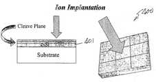
- the methodintroduces a plurality of particles 400 concurrently through each of the donor substrate surface regions to form a cleave region 401 provided by the plurality of particles between the donor substrate thickness and the donor substrate surface region.
- the particlesare implanted through surfaces of at least two or more donor substrate regions and most preferably through each of the donor substrate regions simultaneously for efficiency.
- the cleave regioncan be formed using a variety of techniques. That is, the cleave region can be formed using any suitable combination of implanted particles, deposited layers, diffused materials, patterned regions, and other techniques. Referring again to FIG. 4 , the method introduces certain energetic particles using an implant process through a top surface of each of the donor substrate regions simultaneously to a selected depth, which defines a thickness of the material region, termed the “thin film” of material.
- a variety of techniquescan be used to implant the energetic particles into the silicon wafer according to a specific embodiment. These techniques include ion implantation using, for example, beam line ion implantation equipment manufactured from companies such as Applied Materials, Inc. and others.
- implantationoccurs using a plasma immersion ion implantation (“PIII”) technique, ion shower, and other non-mass specific techniques.
- PIIIplasma immersion ion implantation
- Such techniquescan be particularly effective due to its ability to implant large areas from different substrates simultaneously according to a specific embodiment. Combination of such techniques may also be used.
- Ion implant dose for the non-mass specific techniquesshould be about 10 percent end to end uniformity across the multiple substrates or better.
- Ion implant depth uniformity for the non-mass specific techniquesshould be about 10 percent end to end uniformity across the multiple substrates or better.
- techniques useddepend upon the application.
- smaller mass particlesare generally selected to reduce a possibility of damage to the material region according to a preferred embodiment. That is, smaller mass particles easily travel through the substrate material to the selected depth without substantially damaging the material region that the particles traverse through.
- the smaller mass particlesor energetic particles
- the particlescan be almost any charged (e.g., positive or negative) and or neutral atoms or molecules, or electrons, or the like.
- the particlescan be neutral and or charged particles including ions such as ions of hydrogen and its isotopes, rare gas ions such as helium and its isotopes, and neon, or others depending upon the embodiment.
- the particlescan also be derived from compounds such as gases, e.g., hydrogen gas, water vapor, methane, and hydrogen compounds, and other light atomic mass particles.
- gasese.g., hydrogen gas, water vapor, methane, and hydrogen compounds
- the particlescan be any combination of the above particles, and or ions and or molecular species and or atomic species.
- the particlesgenerally have sufficient kinetic energy to penetrate through the surface to the selected depth underneath the surface.
- Implantation doseranges from about 10 15 to about 10 18 atoms/cm 2 , and preferably the dose is greater than about 1016 atoms/cm 2 .
- Implantation energyranges from about 1 KeV to about 1 MeV, and is generally about 50 KeV.
- Implantation temperatureranges from about 20 to about 600 Degrees Celsius, and is preferably less than about 400 Degrees Celsius to prevent a possibility of a substantial quantity of hydrogen ions from diffusing out of the implanted silicon wafer and annealing the implanted damage and stress.
- the hydrogen ionscan be selectively introduced into the silicon wafer to the selected depth at an accuracy of about +/ ⁇ 0.03 to +/ ⁇ 0.05 microns.
- the type of ion used and process conditionsdepend upon the application.
- the implanted particlesadd stress or reduce fracture energy along a plane parallel to the top surface of the substrate at the selected depth.
- the energiesdepend, in part, upon the implantation species and conditions. These particles reduce a fracture energy level of the substrate at the selected depth. This allows for a controlled cleave along the implanted plane at the selected depth. Implantation can occur under conditions such that the energy state of the substrate at all internal locations is insufficient to initiate a non-reversible fracture (i.e., separation or cleaving) in the substrate material.
- implantationdoes generally cause a certain amount of defects (e.g., micro-detects) in the substrate that can typically at least partially be repaired by subsequent heat treatment, e.g., thermal annealing or rapid thermal annealing.
- subsequent heat treatmente.g., thermal annealing or rapid thermal annealing.
- cleave regionis formed using other processes, such as those using a silicon germanium cleave plane developed by Silicon Genesis Corporation of San Jose, Calif. and processes such as the SmartCutTM process of Soitec SA of France, and the EltranTM process of Canon Inc. of Tokyo, Japan, any like processes, and others.
- processessuch as those using a silicon germanium cleave plane developed by Silicon Genesis Corporation of San Jose, Calif. and processes such as the SmartCutTM process of Soitec SA of France, and the EltranTM process of Canon Inc. of Tokyo, Japan, any like processes, and others.
- SmartCutTM process of Soitec SA of Francethe SmartCutTM process of Soitec SA of France
- EltranTM process of Canon Inc.of Tokyo, Japan, any like processes, and others.
- the methodincludes joining each of the donor substrate surface regions to a handle substrate surface region 501 as illustrated by FIG. 5 .
- the handle substrate surface regionis provided from a handle substrate 503 .
- the handle substrate and donor substrate surfacesare each subjected to a cleaning solution to treat surfaces of the substrates to clean the donor substrate surface regions according to a specific embodiment.
- a solution to clean the substrates and handle substratecan e a mixture of hydrogen peroxide and sulfuric acid and other like solutions according to a specific embodiment.
- a dryercan dry the donor substrates and handle substrate surfaces to remove any residual liquids, particles, and other impurities from the substrate surfaces.
- Self bondingoccurs by placing surfaces of the cleaned substrates (e.g., donor substrate regions and handle substrate) together after an optional plasma activation process depending upon a specific layer transfer process used. If desired, such plasma activated processes clean and/or activate the surfaces of the substrates.
- the plasma activated processesare provided, for example, using an oxygen and/or nitrogen bearing plasma at 20° C. to 40° C. temperature.
- the plasma activated processesare preferably carried out in dual frequency plasma activation system manufactured by Silicon Genesis Corporation of San Jose, Calif. Of course, there can be other variations, modifications, and alternatives, which have been described herein, as well as outside of the present specification.
- each of these substratesis bonded together according to a specific embodiment.
- the handle substratehas been bonded to the plurality of donor substrate surface regions.
- the substratesare preferably bonded using an EVG 850 bonding tool manufactured by Electronic Vision Group or other like processes for smaller substrate sizes such as 200 mm or 300 mm diameter wafers. Other types of tools such as those manufactured by Karl Suss may also be used. Of course, there can be other variations, modifications, and alternatives.
- bonding between the handle substrate and each of the donorsis substantially permanent and has good reliability. For larger glass sizes, custom bonding equipment would be desired but are mostly larger versions of those used to bond together semiconductor substrates according to a specific embodiment.
- the bonded substrate structuresare subjected to a bake treatment.
- the bake treatmentmaintains the bonded substrate at a predetermined temperature and predetermined time.
- the temperatureranges from about 200 or 250 Degrees Celsius to about 400 Degrees Celsius and is preferably about 350 Degrees Celsius for about 1 hour or so for silicon donor substrates and the handle substrate to attach themselves to each other permanently according to the preferred embodiment.
- the temperatureranges from about 200 or 250 Degrees Celsius to about 400 Degrees Celsius and is preferably about 350 Degrees Celsius for about 1 hour or so for silicon donor substrates and the handle substrate to attach themselves to each other permanently according to the preferred embodiment.
- the substratesare joined or fused together using a low temperature thermal step.
- the low temperature thermal processgenerally ensures that the implanted particles do not place excessive stress on the material region, which can produce an uncontrolled cleave action.
- the low temperature bonding processoccurs by a self-bonding process or other like process.
- an adhesivedisposed on either or both surfaces of the substrates, which bond one substrate to another substrate.
- the adhesiveincludes an epoxy, polyimide-type materials, and the like.
- Spin-on-glass layerscan be used to bond one substrate surface onto the face of another. These spin-on-glass (“SOG”) materials include, among others, siloxanes or silicates, which are often mixed with alcohol-based solvents or the like. SOG can be a desirable material because of the low temperatures (e.g., 150 to 250 degrees C.) often needed to cure the SOG after it is applied to surfaces of the wafers.
- a variety of other low temperature techniquescan be used to join the donor substrate surface regions to the handle substrate.
- an electro-static bonding techniquecan be used to join the two substrates together.
- one or both substrate surface(s)is charged to attract to the other substrate surface.
- the donor substrate surfacescan be fused to the handle wafer using a variety of other commonly known techniques. Of course, the technique used depends upon the application.
- the methodincludes a step of initiating a controlled cleaving action 600 within one or more of the donor substrates along a portion of the cleave region.
- the cleaving processcan be a controlled cleaving process using a propagating cleave front to selectively free a thickness of material from each of the donor substrate regions attached to a handle substrate.
- Alternative techniques for cleavingcan also be used. Such techniques, include, but are not limited to those using a silicon germanium cleave region from Silicon Genesis Corporation of San Jose, Calif., the SmartCutTM process of Soitec SA of France, and the EltranTM process of Canon Inc.
- the methodthen removes the transfer substrate, which provided each of the thickness of material from each of the donor substrate regions, from the handle substrate to form a plurality of donor substrate portions spatially disposed overlying the handle substrate surface region.
- the present methodperforms other processes on portions of the donor substrate regions, which have been attached to the handle substrate.
- the methodforms one or more devices on one or more portions of the donor substrate portions spatially disposed overlying the handle substrate surface regions.
- Such devicescan include integrated semiconductor devices, photonic and/or optoelectronic devices (e.g., light valves), piezoelectronic devices, microelectromechanical systems (“MEMS”), nano-technology structures, sensors, actuators, solar cells, flat panel display devices (e.g., LCD, AMLCD), biological and biomedical devices, and the like.
- Such devicescan be made using deposition, etching, implantation, photo masking processes, any combination of these, and the like.
- Additional processesmay include a “reuse” process according to a specific embodiment, as illustrated by FIG. 7 .
- the initial cleaving processremoved a thickness of material from each of the donor substrate regions provided on the transfer substrate.
- the remaining donor substrate regionsmay be subjected to a surface smoothing process, oxidized and implanted again to form another cleave region within each of the donor substrate regions.
- the donor substrate regionswhich now include the plurality of cleave regions, are subjected to a bonding process to another handle substrate and a cleaving process to form a tiled handle substrate including a plurality of donor substrate portions.
- a bonding processto another handle substrate and a cleaving process to form a tiled handle substrate including a plurality of donor substrate portions.
Landscapes
- Physics & Mathematics (AREA)
- Engineering & Computer Science (AREA)
- High Energy & Nuclear Physics (AREA)
- General Physics & Mathematics (AREA)
- Toxicology (AREA)
- Condensed Matter Physics & Semiconductors (AREA)
- Health & Medical Sciences (AREA)
- Manufacturing & Machinery (AREA)
- Computer Hardware Design (AREA)
- Microelectronics & Electronic Packaging (AREA)
- Power Engineering (AREA)
- Spectroscopy & Molecular Physics (AREA)
- Recrystallisation Techniques (AREA)
Abstract
Description
- NOT APPLICABLE
- NOT APPLICABLE
- NOT APPLICABLE
- The present invention relates to the manufacture of substrates. More particularly, the invention provides a technique including a method and a structure for forming multi-layered substrate structures, using a tiled approach, for the fabrication of devices, for example, on flat panel displays. But it will be recognized that the invention has a wider range of applicability; it can also be applied to other substrates for multi-layered integrated circuit devices, three-dimensional packaging of integrated semiconductor devices, photonic devices, piezoelectronic devices, microelectromechanical systems (“MEMS”), nano-technology structures, sensors, actuators, solar cells, biological and biomedical devices, and the like.
- From the very early days, human beings have been building useful articles, tools, or devices using less useful materials for numerous years. In some cases, articles are assembled by way of smaller elements or building blocks. Alternatively, less useful articles are separated into smaller pieces to improve their utility. A common example of these articles to be separated include substrate structures, such as a glass plate, a diamond, a semiconductor substrate, a flat panel display, and others. These substrate structures are often cleaved or separated using a variety of techniques. In some cases, the substrates can be separated using a saw operation. The saw operation generally relies upon a rotating blade or tool, which cuts through the substrate material to separate the substrate material into two pieces. This technique, however, is often extremely “rough” and cannot generally be used for providing precision separations in the substrate for the manufacture of fine tools and assemblies. Additionally, the saw operation often has difficulty separating or cutting extremely hard and or brittle materials, such as diamond or glass. Additionally, the saw operation has difficulty in manufacturing larger substrates for flat panel displays and the like.
- Accordingly, techniques have been developed to fabricate flat panel display substrates. These substrates are often fabricated on large sheets of glass or other like structures. The sheets of glass are subjected to thin film processing at lower temperatures. Amorphous silicon is often used to form thin film transistor devices on these sheets of glass. Amorphous silicon, however, suffers from a variety of known limitations.
- As an example, amorphous silicon often has higher resistance than conventional single crystal silicon. Additionally, amorphous silicon may be difficult to use for high speed device applications due to its low relative carrier mobility. Accordingly, certain techniques have been developed to cleave a thin film of crystalline material from a larger donor substrate portion. These techniques are commonly known as “layer transfer” processes. Such layer transfer processes have been useful in the manufacture of specialized substrate structures, such as silicon on insulator or display substrates. As merely an example, a pioneering technique was developed by Francois J. Henley and Nathan Chung to cleave films of materials. Such technique has been described in U.S. Pat. No. 6,013,563 titled Controlled Cleaving Process, assigned to Silicon Genesis Corporation of San Jose, Calif., and hereby incorporated by reference for all purposes. Although such technique has been successful, there is still a desire for improved ways of manufacturing multilayered structures.
- From the above, it is seen that a technique for manufacturing large substrates which is cost effective and efficient is desirable.
- According to the present invention, techniques related to the manufacture of substrates are provided. More particularly, the invention provides a technique including a method and a structure for forming multi-layered substrate structures, using a tiled approach, for the fabrication of devices, for example, on flat panel displays. But it will be recognized that the invention has a wider range of applicability; it can also be applied to other substrates for multi-layered integrated circuit devices, three-dimensional packaging of integrated semiconductor devices, photonic devices, piezoelectronic devices, microelectromechanical systems (“MEMS”), nano-technology structures, sensors, actuators, solar cells, biological and biomedical devices, and the like.
- In a specific embodiment, the present invention provides a method for forming a plurality of tile structures on a substrate member. The method includes providing a transfer substrate, e.g., glass, semiconductor substrate, quartz, a composite, or other suitable material. In a preferred embodiment, the transfer substrate has a surface region, which has a plurality of donor substrate regions, e.g., silicon, germanium, gallium arsenide, gallium nitride, silicon carbide, other Group III/V materials, Group II/VI materials, any combination of these, and others. Each of the donor substrate regions is characterized by a donor substrate thickness and a donor substrate surface region. Each of the donor substrate regions is spatially disposed overlying the surface region of the transfer substrate. Again in a preferred embodiment, the method implants a plurality of particles concurrently through each of the donor substrate surface regions to form a cleave region provided by the plurality of particles between a portion of the donor substrate thickness and the donor substrate surface region. The method also includes joining each of the donor substrate surface regions to a handle substrate surface region. The handle substrate surface region is provided from a handle substrate. The method includes removing the transfer substrate from the handle substrate to form a plurality of donor substrate portions spatially disposed overlying the handle substrate surface region.
- In an alternative specific embodiment, the present invention provides a reusable transfer substrate member for forming a tiled substrate structure. The member including a transfer substrate, which has a surface region. The surface region comprises a plurality of donor substrate regions. Each of the donor substrate regions is characterized by a donor substrate thickness and a donor substrate surface region. Each of the donor substrate regions is spatially disposed overlying the surface region of the transfer substrate. Each of the donor substrate regions has the donor substrate thickness without a definable cleave region. That is, the donor substrate thickness exists but cannot be cleaved according to a specific embodiment.
- In an alternative specific embodiment, the present invention provides a method for forming a plurality of tile structures on a substrate member, e.g., glass, quartz. The method includes providing a transfer substrate, which has a surface region. The surface region comprises a plurality of donor substrate regions. Each of the donor substrate regions is characterized by a donor substrate thickness and a donor substrate surface region. Each of the donor substrate regions is spatially disposed overlying the surface region of the transfer substrate. The method includes processing the donor substrate regions provided on the transfer substrate concurrently to form a cleave region between a portion of the donor substrate thickness and the donor substrate surface region for each of the donor substrates. Depending upon the embodiment, the processing can be a thermal process, implanting process, etching process, chemical and/or electro-chemical process, any combination of these, and others, which cause a change to a predetermined portion of the donor substrate thickness to form the cleave region, which becomes cleavable from non-cleavable. The method joins each of the donor substrate surface regions to a handle substrate surface region, which is from a handle substrate. The method also includes removing the transfer substrate from the handle substrate to form a plurality of donor substrate portions spatially disposed overlying the handle substrate surface region.
- Numerous benefits are achieved over pre-existing techniques using the present invention. In particular, the present invention uses controlled energy and selected conditions to preferentially cleave a plurality of thin films of material from a plurality of donor substrates, which includes multi-material sandwiched films. This cleaving process selectively removes the plurality of thin films of material from the substrates while preventing a possibility of damage to the film or a remaining portion of the substrate. Additionally, the present method and structures allows for more efficient processing using implantation of a plurality of donor substrates simultaneously according to a specific embodiment. Furthermore, the invention provides a method and structure to form large master donor substrates including a plurality of donor substrate regions using an economical approach and fewer implanting steps, as compared to conventional techniques. Depending upon the embodiment, one or more of these benefits may be achieved. These and other benefits may be described throughout the present specification and more particularly below.
- The present invention achieves these benefits and others in the context of known process technology. However, a further understanding of the nature and advantages of the present invention may be realized by reference to the latter portions of the specification and attached drawings.
FIG. 1 is a simplified diagram illustrating a tiled substrate member according to an embodiment of the present invention;FIG. 2 is a simplified diagram illustrating an alternative tiled substrate member according to an alternative embodiment of the present invention; andFIGS. 3 through 7 illustrate a simplified method for manufacturing a tiled substrate according to embodiments of the present invention- According to the present invention, techniques related to the manufacture of substrates are provided. More particularly, the invention provides a technique including a method and a structure for forming multi-layered substrate structures, using a tiled approach, for the fabrication of devices, for example, on flat panel displays. But it will be recognized that the invention has a wider range of applicability; it can also be applied to other substrates for multi-layered integrated circuit devices, three-dimensional packaging of integrated semiconductor devices, photonic devices, piezoelectronic devices, microelectromechanical systems (“MEMS”), nano-technology structures, sensors, actuators, solar cells, biological and biomedical devices, and the like.
FIG. 1 is a simplified diagram illustrating a master tiledsubstrate member 100 according to an embodiment of the present invention. This diagram is merely an illustration that should not unduly limit the scope of the claims herein. One of ordinary skill in the art would recognize other variations, modifications, and alternatives. As shown, the master tiled substrate member has a plurality ofsubstrates regions 103 disposed spatially on a larger substrate member101. The plurality of substrate regions can be used as a starting material for a plurality of donor substrate regions. The plurality of donor substrate regions can be made of a variety of materials such as silicon, germanium, gallium arsenide, gallium nitride, silicon carbide, other Group III/V materials, Group II/VI materials. The larger substrate member can be any suitable piece to act as a transfer substrate, which will be described in further detail below. The larger substrate is made of a suitable material that is rigid and can hold each of the donor substrate regions in place. Depending upon the embodiment, the substrate regions can be made of a single material, multiple materials, or any combination of these, and the like. Of course, there can be other variations, modifications, and alternatives.FIG. 2 is a simplified diagram illustrating an alternative tiled substrate member including a handle substrate200 according to an alternative embodiment of the present invention. This diagram is merely an illustration that should not unduly limit the scope of the claims herein. One of ordinary skill in the art would recognize other variations, modifications, and alternatives. As shown, thetiled substrates 205 are provided onhandle substrate 201. Each of the tiled substrates is derived from a layer transfer process from the master tiled substrate, which was described above, and throughout the present specification. The layer transfer process may be a controlled cleaving process from Silicon Genesis Corporation of San Jose, Calif., a process called Eltran™ from Canon, Inc., of Japan and other processes, such as thermal treatment processes called SmartCut™ from Soitec, SA of France. Of course, there can be other variations, modifications, and alternatives. Details of methods according to embodiments of the present invention are provided throughout the present specification and more particularly below.- A method for fabricating a large area substrate using a tiled approach according to an embodiment of the present invention may be outlined as follows:
- 1. Provide a transfer substrate, the transfer substrate having a surface region;
- 2. Spatially disposing a plurality of donor substrate regions on the surface region of the transfer substrate, each of the donor substrate regions may be characterized by a donor substrate thickness and a donor substrate surface region;
- 3. Implant a plurality of particles concurrently through each of the donor substrate surface regions to form a cleave region provided by the plurality of particles between the donor substrate thickness and the donor substrate surface region;
- 4. Join each of the donor substrate surface regions to a handle substrate surface region, the handle substrate surface region being provided from a handle substrate; and
- 5. Initiate a controlled cleaving action within one or more of the donor substrates;
- 6. Remove the transfer substrate from the handle substrate to form a plurality of donor substrate portions spatially disposed overlying the handle substrate surface region;
- 7. Form one or more devices on one or more portions of the donor substrate portions spatially disposed overlying the handle substrate surface region; and
- 8. Perform other steps, as desired.
- The above sequence of steps provides a method according to an embodiment of the present invention. As shown, the method uses a combination of steps including a way of forming a large substrate material using a plurality of donor substrates that are manufactured concurrently during a portion of their processing. Other alternatives can also be provided where steps are added, one or more steps are removed, or one or more steps are provided in a different sequence without departing from the scope of the claims herein. Further details of the present method can be found throughout the present specification and more particularly below.
- The above sequence of steps provides a method according to an embodiment of the present invention. As shown, the method uses a combination of steps including a way of forming a large substrate material using a plurality of donor substrates that are manufactured concurrently during a portion of their processing. Other alternatives can also be provided where steps are added, one or more steps are removed, or one or more steps are provided in a different sequence without departing from the scope of the claims herein. Further details of the present method can be found throughout the present specification and more particularly below.
FIGS. 3 through 7 illustrate a simplified method for manufacturing a tiled substrate according to embodiments of the present invention. These diagrams are merely illustrations that should not unduly limit the scope of the claims herein. One of ordinary skill in the art would recognize other variations, modifications, and alternatives. As shown, the method begins by providing atransfer substrate 303, which has asurface region 303. The transfer substrate can be made of any suitable material such as a conductor, insulator, or semiconductor, which may be a composite, single layer, or multiple layers, or any combination of these, and the like. The conductor can be a metal such as aluminum, stainless steel, or other metal materials. The insulator can be a glass, a plastic, a quartz, or a ceramic, or combination of these, and the like. The semiconductor can be silicon, germanium, gallium arsenide, silicon-germanium alloy, any Group III/V materials, and others. The transfer substrate can be made of a single homogenous material, or a combination of various layers, depending upon the specific embodiment. Of course, there can be other variations, modifications, and alternatives.- As shown, the transfer substrate has a plurality of
donor substrate regions 305 on the surface region of the transfer substrate according to a specific embodiment. Each of the donor substrate regions may be characterized by a donor substrate thickness and a donor substrate surface region. The plurality of donor substrate regions can be made of a variety of materials such as silicon, germanium, gallium arsenide, gallium nitride, silicon carbide, other Group III/V materials, Group II/VI materials. Each of the donor substrate regions is smaller in size then the transfer substrate, which often has at least two times, three times, four times or greater a surface region of any individual donor substrate region. For example, a Generation 3.5 glass size (which is an industrial standard for the flat panel display industry) suitable for flat panel manufacturing is 620 mm×750 mm and is roughly 7.5 times larger in area than a 300 mm single crystal silicon substrate. Alternatively, the handle substrate may be much larger than Generation 3.5. The area ratio would also be proportionally larger if the round 300 mm substrate would be cut to tile the transfer substrate according to a specific embodiment. - In a preferred embodiment, each of the donor substrate regions is temporarily (or permanently) transferred onto a spatial surface region of the transfer substrate. Once this bonding occurs, the transfer substrate can be handled and used as a larger effective donor substrate according to a specific embodiment. The donor substrate regions can each be oxidized307 and then bonded to the surface region of a handle substrate, as shown. As merely an example, the oxidation layer is often formed on a silicon substrate. The oxidation layer can be a natural oxide, thermal oxide, deposited oxide, or any other type of oxide layer, which enhanced bonding the donor substrate regions on the transfer substrate. In a specific embodiment, the method performs a cleaning and/or activating process (e.g., plasma activated process) on surfaces of the donor substrate regions, which have been oxidized, and the transfer substrate according to a specific embodiment. Such plasma activating processes clean and/or activate the surfaces of the substrates. The plasma activated processes are provided using a nitrogen bearing plasma at 20° C.-40° C. temperature. The plasma activated processes are preferably carried out in dual frequency plasma activation system manufactured by Silicon Genesis Corporation of San Jose, Calif. Of course, there can be other variations, modifications, and alternatives.
- Referring now to
FIG. 4 , the method introduces a plurality of particles400 concurrently through each of the donor substrate surface regions to form acleave region 401 provided by the plurality of particles between the donor substrate thickness and the donor substrate surface region. In a preferred embodiment, the particles are implanted through surfaces of at least two or more donor substrate regions and most preferably through each of the donor substrate regions simultaneously for efficiency. - Depending upon the embodiment, the cleave region can be formed using a variety of techniques. That is, the cleave region can be formed using any suitable combination of implanted particles, deposited layers, diffused materials, patterned regions, and other techniques. Referring again to
FIG. 4 , the method introduces certain energetic particles using an implant process through a top surface of each of the donor substrate regions simultaneously to a selected depth, which defines a thickness of the material region, termed the “thin film” of material. A variety of techniques can be used to implant the energetic particles into the silicon wafer according to a specific embodiment. These techniques include ion implantation using, for example, beam line ion implantation equipment manufactured from companies such as Applied Materials, Inc. and others. Alternatively, implantation occurs using a plasma immersion ion implantation (“PIII”) technique, ion shower, and other non-mass specific techniques. Such techniques can be particularly effective due to its ability to implant large areas from different substrates simultaneously according to a specific embodiment. Combination of such techniques may also be used. Ion implant dose for the non-mass specific techniques should be about 10 percent end to end uniformity across the multiple substrates or better. Ion implant depth uniformity for the non-mass specific techniques should be about 10 percent end to end uniformity across the multiple substrates or better. Of course, techniques used depend upon the application. - Depending upon the application, smaller mass particles are generally selected to reduce a possibility of damage to the material region according to a preferred embodiment. That is, smaller mass particles easily travel through the substrate material to the selected depth without substantially damaging the material region that the particles traverse through. For example, the smaller mass particles (or energetic particles) can be almost any charged (e.g., positive or negative) and or neutral atoms or molecules, or electrons, or the like. In a specific embodiment, the particles can be neutral and or charged particles including ions such as ions of hydrogen and its isotopes, rare gas ions such as helium and its isotopes, and neon, or others depending upon the embodiment. The particles can also be derived from compounds such as gases, e.g., hydrogen gas, water vapor, methane, and hydrogen compounds, and other light atomic mass particles. Alternatively, the particles can be any combination of the above particles, and or ions and or molecular species and or atomic species. The particles generally have sufficient kinetic energy to penetrate through the surface to the selected depth underneath the surface.
- Using hydrogen as the implanted species into the silicon wafer as an example, the implantation process is performed using a specific set of conditions. Implantation dose ranges from about 1015to about 1018atoms/cm2, and preferably the dose is greater than about 1016 atoms/cm2. Implantation energy ranges from about 1 KeV to about 1 MeV, and is generally about 50 KeV. Implantation temperature ranges from about 20 to about 600 Degrees Celsius, and is preferably less than about 400 Degrees Celsius to prevent a possibility of a substantial quantity of hydrogen ions from diffusing out of the implanted silicon wafer and annealing the implanted damage and stress. The hydrogen ions can be selectively introduced into the silicon wafer to the selected depth at an accuracy of about +/−0.03 to +/−0.05 microns. Of course, the type of ion used and process conditions depend upon the application.
- Effectively, the implanted particles add stress or reduce fracture energy along a plane parallel to the top surface of the substrate at the selected depth. The energies depend, in part, upon the implantation species and conditions. These particles reduce a fracture energy level of the substrate at the selected depth. This allows for a controlled cleave along the implanted plane at the selected depth. Implantation can occur under conditions such that the energy state of the substrate at all internal locations is insufficient to initiate a non-reversible fracture (i.e., separation or cleaving) in the substrate material. It should be noted, however, that implantation does generally cause a certain amount of defects (e.g., micro-detects) in the substrate that can typically at least partially be repaired by subsequent heat treatment, e.g., thermal annealing or rapid thermal annealing. Of course, there can be other variations, modifications, and alternatives.
- Depending upon the embodiment, there may be other techniques for forming a cleave region and/or cleave layer. As merely an example, such cleave region is formed using other processes, such as those using a silicon germanium cleave plane developed by Silicon Genesis Corporation of San Jose, Calif. and processes such as the SmartCut™ process of Soitec SA of France, and the Eltran™ process of Canon Inc. of Tokyo, Japan, any like processes, and others. Of course, there may be other variations, modifications, and alternatives.
- In a specific embodiment, the method includes joining each of the donor substrate surface regions to a handle
substrate surface region 501 as illustrated byFIG. 5 . As shown, the handle substrate surface region is provided from ahandle substrate 503. Before joining, the handle substrate and donor substrate surfaces are each subjected to a cleaning solution to treat surfaces of the substrates to clean the donor substrate surface regions according to a specific embodiment. An example of a solution to clean the substrates and handle substrate can e a mixture of hydrogen peroxide and sulfuric acid and other like solutions according to a specific embodiment. A dryer can dry the donor substrates and handle substrate surfaces to remove any residual liquids, particles, and other impurities from the substrate surfaces. Self bonding occurs by placing surfaces of the cleaned substrates (e.g., donor substrate regions and handle substrate) together after an optional plasma activation process depending upon a specific layer transfer process used. If desired, such plasma activated processes clean and/or activate the surfaces of the substrates. The plasma activated processes are provided, for example, using an oxygen and/or nitrogen bearing plasma at 20° C. to 40° C. temperature. The plasma activated processes are preferably carried out in dual frequency plasma activation system manufactured by Silicon Genesis Corporation of San Jose, Calif. Of course, there can be other variations, modifications, and alternatives, which have been described herein, as well as outside of the present specification. - Thereafter, each of these substrates is bonded together according to a specific embodiment. As shown, the handle substrate has been bonded to the plurality of donor substrate surface regions. The substrates are preferably bonded using an EVG 850 bonding tool manufactured by Electronic Vision Group or other like processes for smaller substrate sizes such as 200 mm or 300 mm diameter wafers. Other types of tools such as those manufactured by Karl Suss may also be used. Of course, there can be other variations, modifications, and alternatives. Preferably, bonding between the handle substrate and each of the donors is substantially permanent and has good reliability. For larger glass sizes, custom bonding equipment would be desired but are mostly larger versions of those used to bond together semiconductor substrates according to a specific embodiment.
- Accordingly after bonding, the bonded substrate structures are subjected to a bake treatment. The bake treatment maintains the bonded substrate at a predetermined temperature and predetermined time. Preferably, the temperature ranges from about 200 or 250 Degrees Celsius to about 400 Degrees Celsius and is preferably about 350 Degrees Celsius for about 1 hour or so for silicon donor substrates and the handle substrate to attach themselves to each other permanently according to the preferred embodiment. Depending upon the specific application, there can be other variations, modifications, and alternatives.
- In a specific embodiment, the substrates are joined or fused together using a low temperature thermal step. The low temperature thermal process generally ensures that the implanted particles do not place excessive stress on the material region, which can produce an uncontrolled cleave action. In a specific embodiment, the low temperature bonding process occurs by a self-bonding process or other like process. Alternatively, an adhesive disposed on either or both surfaces of the substrates, which bond one substrate to another substrate. In a specific embodiment, the adhesive includes an epoxy, polyimide-type materials, and the like. Spin-on-glass layers can be used to bond one substrate surface onto the face of another. These spin-on-glass (“SOG”) materials include, among others, siloxanes or silicates, which are often mixed with alcohol-based solvents or the like. SOG can be a desirable material because of the low temperatures (e.g., 150 to 250 degrees C.) often needed to cure the SOG after it is applied to surfaces of the wafers.
- Alternatively, a variety of other low temperature techniques can be used to join the donor substrate surface regions to the handle substrate. For instance, an electro-static bonding technique can be used to join the two substrates together. In particular, one or both substrate surface(s) is charged to attract to the other substrate surface. Additionally, the donor substrate surfaces can be fused to the handle wafer using a variety of other commonly known techniques. Of course, the technique used depends upon the application.
- Referring to
FIG. 6 , the method includes a step of initiating a controlled cleaving action600 within one or more of the donor substrates along a portion of the cleave region. Depending upon the specific embodiment, there can be certain variations. For example, the cleaving process can be a controlled cleaving process using a propagating cleave front to selectively free a thickness of material from each of the donor substrate regions attached to a handle substrate. Alternative techniques for cleaving can also be used. Such techniques, include, but are not limited to those using a silicon germanium cleave region from Silicon Genesis Corporation of San Jose, Calif., the SmartCut™ process of Soitec SA of France, and the Eltran™ process of Canon Inc. of Tokyo, Japan, any like processes, and others. The method then removes the transfer substrate, which provided each of the thickness of material from each of the donor substrate regions, from the handle substrate to form a plurality of donor substrate portions spatially disposed overlying the handle substrate surface region. - Next, the present method performs other processes on portions of the donor substrate regions, which have been attached to the handle substrate. The method forms one or more devices on one or more portions of the donor substrate portions spatially disposed overlying the handle substrate surface regions. Such devices can include integrated semiconductor devices, photonic and/or optoelectronic devices (e.g., light valves), piezoelectronic devices, microelectromechanical systems (“MEMS”), nano-technology structures, sensors, actuators, solar cells, flat panel display devices (e.g., LCD, AMLCD), biological and biomedical devices, and the like. Such devices can be made using deposition, etching, implantation, photo masking processes, any combination of these, and the like. Of course, there can be other variations, modifications, and alternatives. Additionally, other steps can also be formed, as desired.
- Additional processes may include a “reuse” process according to a specific embodiment, as illustrated by
FIG. 7 . As shown, the initial cleaving process removed a thickness of material from each of the donor substrate regions provided on the transfer substrate. The remaining donor substrate regions may be subjected to a surface smoothing process, oxidized and implanted again to form another cleave region within each of the donor substrate regions. The donor substrate regions, which now include the plurality of cleave regions, are subjected to a bonding process to another handle substrate and a cleaving process to form a tiled handle substrate including a plurality of donor substrate portions. Of course, there can be other variations, modifications, and alternatives. - While the above is a full description of the specific embodiments, various modifications, alternative constructions and equivalents may be used. Therefore, the above description and illustrations should not be taken as limiting the scope of the present invention which is defined by the appended claims.
Claims (28)
Priority Applications (8)
| Application Number | Priority Date | Filing Date | Title |
|---|---|---|---|
| US11/191,464US7674687B2 (en) | 2005-07-27 | 2005-07-27 | Method and structure for fabricating multiple tiled regions onto a plate using a controlled cleaving process |
| KR1020087004648AKR20080042095A (en) | 2005-07-27 | 2006-07-26 | Method and structure for fabricating multiple tile regions on a plate using controlled cleaving treatment |
| JP2008524186AJP2009507363A (en) | 2005-07-27 | 2006-07-26 | Method and structure for forming multiple tile portions on a plate using a controlled cleavage process |
| PCT/US2006/029378WO2007014320A2 (en) | 2005-07-27 | 2006-07-26 | Method and structure for fabricating multiple tile regions onto a plate using a controlled cleaving process |
| TW095127459ATW200746277A (en) | 2005-07-27 | 2006-07-27 | Method and structure for fabricating multiple tile regions onto a plate using a controlled cleaving process |
| US12/695,027US8012855B2 (en) | 2005-07-27 | 2010-01-27 | Method and structure for fabricating multiple tiled regions onto a plate using a controlled cleaving process |
| US12/695,036US8071463B2 (en) | 2005-07-27 | 2010-01-27 | Method and structure for fabricating multiple tiled regions onto a plate using a controlled cleaving process |
| US12/695,008US7911016B2 (en) | 2005-07-27 | 2010-01-27 | Method and structure for fabricating multiple tiled regions onto a plate using a controlled cleaving process |
Applications Claiming Priority (1)
| Application Number | Priority Date | Filing Date | Title |
|---|---|---|---|
| US11/191,464US7674687B2 (en) | 2005-07-27 | 2005-07-27 | Method and structure for fabricating multiple tiled regions onto a plate using a controlled cleaving process |
Related Child Applications (3)
| Application Number | Title | Priority Date | Filing Date |
|---|---|---|---|
| US12/695,036ContinuationUS8071463B2 (en) | 2005-07-27 | 2010-01-27 | Method and structure for fabricating multiple tiled regions onto a plate using a controlled cleaving process |
| US12/695,027ContinuationUS8012855B2 (en) | 2005-07-27 | 2010-01-27 | Method and structure for fabricating multiple tiled regions onto a plate using a controlled cleaving process |
| US12/695,008DivisionUS7911016B2 (en) | 2005-07-27 | 2010-01-27 | Method and structure for fabricating multiple tiled regions onto a plate using a controlled cleaving process |
Publications (2)
| Publication Number | Publication Date |
|---|---|
| US20070026638A1true US20070026638A1 (en) | 2007-02-01 |
| US7674687B2 US7674687B2 (en) | 2010-03-09 |
Family
ID=37694921
Family Applications (4)
| Application Number | Title | Priority Date | Filing Date |
|---|---|---|---|
| US11/191,464Expired - Fee RelatedUS7674687B2 (en) | 2005-07-27 | 2005-07-27 | Method and structure for fabricating multiple tiled regions onto a plate using a controlled cleaving process |
| US12/695,036Expired - Fee RelatedUS8071463B2 (en) | 2005-07-27 | 2010-01-27 | Method and structure for fabricating multiple tiled regions onto a plate using a controlled cleaving process |
| US12/695,027Expired - Fee RelatedUS8012855B2 (en) | 2005-07-27 | 2010-01-27 | Method and structure for fabricating multiple tiled regions onto a plate using a controlled cleaving process |
| US12/695,008Expired - Fee RelatedUS7911016B2 (en) | 2005-07-27 | 2010-01-27 | Method and structure for fabricating multiple tiled regions onto a plate using a controlled cleaving process |
Family Applications After (3)
| Application Number | Title | Priority Date | Filing Date |
|---|---|---|---|
| US12/695,036Expired - Fee RelatedUS8071463B2 (en) | 2005-07-27 | 2010-01-27 | Method and structure for fabricating multiple tiled regions onto a plate using a controlled cleaving process |
| US12/695,027Expired - Fee RelatedUS8012855B2 (en) | 2005-07-27 | 2010-01-27 | Method and structure for fabricating multiple tiled regions onto a plate using a controlled cleaving process |
| US12/695,008Expired - Fee RelatedUS7911016B2 (en) | 2005-07-27 | 2010-01-27 | Method and structure for fabricating multiple tiled regions onto a plate using a controlled cleaving process |
Country Status (1)
| Country | Link |
|---|---|
| US (4) | US7674687B2 (en) |
Cited By (15)
| Publication number | Priority date | Publication date | Assignee | Title |
|---|---|---|---|---|
| US20080160661A1 (en)* | 2006-04-05 | 2008-07-03 | Silicon Genesis Corporation | Method and structure for fabricating solar cells using a layer transfer process |
| US20080315350A1 (en)* | 2007-06-25 | 2008-12-25 | Semiconductor Energy Laboratory Co., Ltd. | Method for manufacturing semiconductor substrate, and semiconductor device |
| US20090004823A1 (en)* | 2007-06-28 | 2009-01-01 | Semiconductor Energy Laboratory Co., Ltd. | Manufacturing method of semiconductor |
| US20090017581A1 (en)* | 2007-07-13 | 2009-01-15 | Semiconductor Energy Laboratory Co., Ltd. | Method for manufacturing a semiconductor device |
| US20090075408A1 (en)* | 2007-09-14 | 2009-03-19 | Semiconductor Energy Laboratory Co., Ltd. | Method for manufacturing soi substrate and method for manufacturing semiconductor device |
| US20090325363A1 (en)* | 2008-06-25 | 2009-12-31 | Semiconductor Energy Laboratory Co., Ltd. | Method for manufacturing soi substrate |
| US20100047997A1 (en)* | 2008-07-22 | 2010-02-25 | Akihiro Ishizuka | Method for manufacturing soi substrate |
| US7927975B2 (en) | 2009-02-04 | 2011-04-19 | Micron Technology, Inc. | Semiconductor material manufacture |
| US20110214806A1 (en)* | 2008-12-01 | 2011-09-08 | Bruno Ghyselen | Ingot formed from basic ingots, wafer made from said ingot and associated method |
| US8431451B2 (en) | 2007-06-29 | 2013-04-30 | Semicondutor Energy Laboratory Co., Ltd. | Display device and method for manufacturing the same |
| TWI470682B (en)* | 2007-09-21 | 2015-01-21 | Semiconductor Energy Lab | Substrate provided with semiconductor film and method of manufacturing the same |
| US8946820B2 (en) | 2011-06-30 | 2015-02-03 | Sharp Kabushiki Kaisha | Method for manufacturing semiconductor substrate, substrate for forming semiconductor substrate, stacked substrate, semiconductor substrate, and electronic device |
| US8981519B2 (en) | 2010-11-05 | 2015-03-17 | Sharp Kabushiki Kaisha | Semiconductor substrate, method of manufacturing semiconductor substrate, thin film transistor, semiconductor circuit, liquid crystal display apparatus, electroluminescence apparatus, wireless communication apparatus, and light emitting apparatus |
| US9041147B2 (en) | 2012-01-10 | 2015-05-26 | Sharp Kabushiki Kaisha | Semiconductor substrate, thin film transistor, semiconductor circuit, liquid crystal display apparatus, electroluminescent apparatus, semiconductor substrate manufacturing method, and semiconductor substrate manufacturing apparatus |
| EP2269230A4 (en)* | 2008-03-08 | 2016-03-30 | Crystal Solar Inc | INTEGRATED METHOD AND SYSTEM FOR MANUFACTURING MONOLITHIC PANELS OF CRYSTALLINE SOLAR CELLS |
Families Citing this family (250)
| Publication number | Priority date | Publication date | Assignee | Title |
|---|---|---|---|---|
| US8153513B2 (en)* | 2006-07-25 | 2012-04-10 | Silicon Genesis Corporation | Method and system for continuous large-area scanning implantation process |
| CN101281912B (en) | 2007-04-03 | 2013-01-23 | 株式会社半导体能源研究所 | Soi substrate and manufacturing method thereof, and semiconductor device |
| EP1993127B1 (en)* | 2007-05-18 | 2013-04-24 | Semiconductor Energy Laboratory Co., Ltd. | Manufacturing method of SOI substrate |
| JP5507063B2 (en) | 2007-07-09 | 2014-05-28 | 株式会社半導体エネルギー研究所 | Method for manufacturing semiconductor device |
| TWI437696B (en) | 2007-09-21 | 2014-05-11 | Semiconductor Energy Lab | Semiconductor device and method of manufacturing same |
| JP5325404B2 (en)* | 2007-09-21 | 2013-10-23 | 株式会社半導体エネルギー研究所 | Method for manufacturing SOI substrate |
| JP2009135430A (en)* | 2007-10-10 | 2009-06-18 | Semiconductor Energy Lab Co Ltd | Method for manufacturing semiconductor device |
| US20090139558A1 (en)* | 2007-11-29 | 2009-06-04 | Shunpei Yamazaki | Photoelectric conversion device and manufacturing method thereof |
| JP5404064B2 (en) | 2008-01-16 | 2014-01-29 | 株式会社半導体エネルギー研究所 | Laser processing apparatus and semiconductor substrate manufacturing method |
| US7947570B2 (en)* | 2008-01-16 | 2011-05-24 | Semiconductor Energy Laboratory Co., Ltd. | Manufacturing method and manufacturing apparatus of semiconductor substrate |
| US8178419B2 (en) | 2008-02-05 | 2012-05-15 | Twin Creeks Technologies, Inc. | Method to texture a lamina surface within a photovoltaic cell |
| CN102150278A (en)* | 2008-06-11 | 2011-08-10 | 因特瓦克公司 | Formation of solar cell-selective emitter using implant and anneal method |
| JP2012521642A (en)* | 2009-03-20 | 2012-09-13 | インテバック・インコーポレイテッド | Solar cell and manufacturing method thereof |
| US8058137B1 (en) | 2009-04-14 | 2011-11-15 | Monolithic 3D Inc. | Method for fabrication of a semiconductor device and structure |
| US8362482B2 (en) | 2009-04-14 | 2013-01-29 | Monolithic 3D Inc. | Semiconductor device and structure |
| US8378715B2 (en) | 2009-04-14 | 2013-02-19 | Monolithic 3D Inc. | Method to construct systems |
| US8405420B2 (en) | 2009-04-14 | 2013-03-26 | Monolithic 3D Inc. | System comprising a semiconductor device and structure |
| US8384426B2 (en) | 2009-04-14 | 2013-02-26 | Monolithic 3D Inc. | Semiconductor device and structure |
| US8669778B1 (en) | 2009-04-14 | 2014-03-11 | Monolithic 3D Inc. | Method for design and manufacturing of a 3D semiconductor device |
| US9509313B2 (en) | 2009-04-14 | 2016-11-29 | Monolithic 3D Inc. | 3D semiconductor device |
| US7986042B2 (en) | 2009-04-14 | 2011-07-26 | Monolithic 3D Inc. | Method for fabrication of a semiconductor device and structure |
| US9711407B2 (en) | 2009-04-14 | 2017-07-18 | Monolithic 3D Inc. | Method of manufacturing a three dimensional integrated circuit by transfer of a mono-crystalline layer |
| US8395191B2 (en) | 2009-10-12 | 2013-03-12 | Monolithic 3D Inc. | Semiconductor device and structure |
| US8362800B2 (en) | 2010-10-13 | 2013-01-29 | Monolithic 3D Inc. | 3D semiconductor device including field repairable logics |
| US8427200B2 (en) | 2009-04-14 | 2013-04-23 | Monolithic 3D Inc. | 3D semiconductor device |
| US8754533B2 (en) | 2009-04-14 | 2014-06-17 | Monolithic 3D Inc. | Monolithic three-dimensional semiconductor device and structure |
| US9577642B2 (en) | 2009-04-14 | 2017-02-21 | Monolithic 3D Inc. | Method to form a 3D semiconductor device |
| US8373439B2 (en) | 2009-04-14 | 2013-02-12 | Monolithic 3D Inc. | 3D semiconductor device |
| US8258810B2 (en) | 2010-09-30 | 2012-09-04 | Monolithic 3D Inc. | 3D semiconductor device |
| US8749053B2 (en)* | 2009-06-23 | 2014-06-10 | Intevac, Inc. | Plasma grid implant system for use in solar cell fabrications |
| US10366970B2 (en) | 2009-10-12 | 2019-07-30 | Monolithic 3D Inc. | 3D semiconductor device and structure |
| US10354995B2 (en) | 2009-10-12 | 2019-07-16 | Monolithic 3D Inc. | Semiconductor memory device and structure |
| US11374118B2 (en) | 2009-10-12 | 2022-06-28 | Monolithic 3D Inc. | Method to form a 3D integrated circuit |
| US8581349B1 (en) | 2011-05-02 | 2013-11-12 | Monolithic 3D Inc. | 3D memory semiconductor device and structure |
| US12027518B1 (en) | 2009-10-12 | 2024-07-02 | Monolithic 3D Inc. | 3D semiconductor devices and structures with metal layers |
| US11018133B2 (en) | 2009-10-12 | 2021-05-25 | Monolithic 3D Inc. | 3D integrated circuit |
| US10043781B2 (en) | 2009-10-12 | 2018-08-07 | Monolithic 3D Inc. | 3D semiconductor device and structure |
| US8476145B2 (en) | 2010-10-13 | 2013-07-02 | Monolithic 3D Inc. | Method of fabricating a semiconductor device and structure |
| US10388863B2 (en) | 2009-10-12 | 2019-08-20 | Monolithic 3D Inc. | 3D memory device and structure |
| US11984445B2 (en) | 2009-10-12 | 2024-05-14 | Monolithic 3D Inc. | 3D semiconductor devices and structures with metal layers |
| US8536023B2 (en) | 2010-11-22 | 2013-09-17 | Monolithic 3D Inc. | Method of manufacturing a semiconductor device and structure |
| US10157909B2 (en) | 2009-10-12 | 2018-12-18 | Monolithic 3D Inc. | 3D semiconductor device and structure |
| US10910364B2 (en) | 2009-10-12 | 2021-02-02 | Monolitaic 3D Inc. | 3D semiconductor device |
| US9099424B1 (en) | 2012-08-10 | 2015-08-04 | Monolithic 3D Inc. | Semiconductor system, device and structure with heat removal |
| US8742476B1 (en) | 2012-11-27 | 2014-06-03 | Monolithic 3D Inc. | Semiconductor device and structure |
| US8450804B2 (en) | 2011-03-06 | 2013-05-28 | Monolithic 3D Inc. | Semiconductor device and structure for heat removal |
| US8148728B2 (en) | 2009-10-12 | 2012-04-03 | Monolithic 3D, Inc. | Method for fabrication of a semiconductor device and structure |
| US8288249B2 (en)* | 2010-01-26 | 2012-10-16 | Semiconductor Energy Laboratory Co., Ltd. | Method for manufacturing SOI substrate |
| SG183267A1 (en)* | 2010-02-09 | 2012-09-27 | Intevac Inc | An adjustable shadow mask assembly for use in solar cell fabrications |
| US8298875B1 (en) | 2011-03-06 | 2012-10-30 | Monolithic 3D Inc. | Method for fabrication of a semiconductor device and structure |
| US8541819B1 (en) | 2010-12-09 | 2013-09-24 | Monolithic 3D Inc. | Semiconductor device and structure |
| US9099526B2 (en) | 2010-02-16 | 2015-08-04 | Monolithic 3D Inc. | Integrated circuit device and structure |
| US8492886B2 (en) | 2010-02-16 | 2013-07-23 | Monolithic 3D Inc | 3D integrated circuit with logic |
| US8026521B1 (en) | 2010-10-11 | 2011-09-27 | Monolithic 3D Inc. | Semiconductor device and structure |
| US8461035B1 (en) | 2010-09-30 | 2013-06-11 | Monolithic 3D Inc. | Method for fabrication of a semiconductor device and structure |
| US8373230B1 (en) | 2010-10-13 | 2013-02-12 | Monolithic 3D Inc. | Method for fabrication of a semiconductor device and structure |
| US9219005B2 (en) | 2011-06-28 | 2015-12-22 | Monolithic 3D Inc. | Semiconductor system and device |
| US9953925B2 (en) | 2011-06-28 | 2018-04-24 | Monolithic 3D Inc. | Semiconductor system and device |
| US10217667B2 (en) | 2011-06-28 | 2019-02-26 | Monolithic 3D Inc. | 3D semiconductor device, fabrication method and system |
| US8642416B2 (en) | 2010-07-30 | 2014-02-04 | Monolithic 3D Inc. | Method of forming three dimensional integrated circuit devices using layer transfer technique |
| US8901613B2 (en) | 2011-03-06 | 2014-12-02 | Monolithic 3D Inc. | Semiconductor device and structure for heat removal |
| US12362219B2 (en) | 2010-11-18 | 2025-07-15 | Monolithic 3D Inc. | 3D semiconductor memory device and structure |
| US11482440B2 (en) | 2010-12-16 | 2022-10-25 | Monolithic 3D Inc. | 3D semiconductor device and structure with a built-in test circuit for repairing faulty circuits |
| US10497713B2 (en) | 2010-11-18 | 2019-12-03 | Monolithic 3D Inc. | 3D semiconductor memory device and structure |
| US8273610B2 (en) | 2010-11-18 | 2012-09-25 | Monolithic 3D Inc. | Method of constructing a semiconductor device and structure |
| US8163581B1 (en) | 2010-10-13 | 2012-04-24 | Monolith IC 3D | Semiconductor and optoelectronic devices |
| US10290682B2 (en) | 2010-10-11 | 2019-05-14 | Monolithic 3D Inc. | 3D IC semiconductor device and structure with stacked memory |
| US11227897B2 (en) | 2010-10-11 | 2022-01-18 | Monolithic 3D Inc. | Method for producing a 3D semiconductor memory device and structure |
| US11024673B1 (en) | 2010-10-11 | 2021-06-01 | Monolithic 3D Inc. | 3D semiconductor device and structure |
| US11158674B2 (en) | 2010-10-11 | 2021-10-26 | Monolithic 3D Inc. | Method to produce a 3D semiconductor device and structure |
| US8114757B1 (en) | 2010-10-11 | 2012-02-14 | Monolithic 3D Inc. | Semiconductor device and structure |
| US11469271B2 (en) | 2010-10-11 | 2022-10-11 | Monolithic 3D Inc. | Method to produce 3D semiconductor devices and structures with memory |
| US11600667B1 (en) | 2010-10-11 | 2023-03-07 | Monolithic 3D Inc. | Method to produce 3D semiconductor devices and structures with memory |
| US11018191B1 (en) | 2010-10-11 | 2021-05-25 | Monolithic 3D Inc. | 3D semiconductor device and structure |
| US11257867B1 (en) | 2010-10-11 | 2022-02-22 | Monolithic 3D Inc. | 3D semiconductor device and structure with oxide bonds |
| US11315980B1 (en) | 2010-10-11 | 2022-04-26 | Monolithic 3D Inc. | 3D semiconductor device and structure with transistors |
| US10896931B1 (en) | 2010-10-11 | 2021-01-19 | Monolithic 3D Inc. | 3D semiconductor device and structure |
| US8379458B1 (en) | 2010-10-13 | 2013-02-19 | Monolithic 3D Inc. | Semiconductor device and structure |
| US11063071B1 (en) | 2010-10-13 | 2021-07-13 | Monolithic 3D Inc. | Multilevel semiconductor device and structure with waveguides |
| US11163112B2 (en) | 2010-10-13 | 2021-11-02 | Monolithic 3D Inc. | Multilevel semiconductor device and structure with electromagnetic modulators |
| US11694922B2 (en) | 2010-10-13 | 2023-07-04 | Monolithic 3D Inc. | Multilevel semiconductor device and structure with oxide bonding |
| US11984438B2 (en) | 2010-10-13 | 2024-05-14 | Monolithic 3D Inc. | Multilevel semiconductor device and structure with oxide bonding |
| US11133344B2 (en) | 2010-10-13 | 2021-09-28 | Monolithic 3D Inc. | Multilevel semiconductor device and structure with image sensors |
| US11164898B2 (en) | 2010-10-13 | 2021-11-02 | Monolithic 3D Inc. | Multilevel semiconductor device and structure |
| US12094892B2 (en) | 2010-10-13 | 2024-09-17 | Monolithic 3D Inc. | 3D micro display device and structure |
| US11605663B2 (en) | 2010-10-13 | 2023-03-14 | Monolithic 3D Inc. | Multilevel semiconductor device and structure with image sensors and wafer bonding |
| US10943934B2 (en) | 2010-10-13 | 2021-03-09 | Monolithic 3D Inc. | Multilevel semiconductor device and structure |
| US12360310B2 (en) | 2010-10-13 | 2025-07-15 | Monolithic 3D Inc. | Multilevel semiconductor device and structure with oxide bonding |
| US11404466B2 (en) | 2010-10-13 | 2022-08-02 | Monolithic 3D Inc. | Multilevel semiconductor device and structure with image sensors |
| US11855114B2 (en) | 2010-10-13 | 2023-12-26 | Monolithic 3D Inc. | Multilevel semiconductor device and structure with image sensors and wafer bonding |
| US11437368B2 (en) | 2010-10-13 | 2022-09-06 | Monolithic 3D Inc. | Multilevel semiconductor device and structure with oxide bonding |
| US10978501B1 (en) | 2010-10-13 | 2021-04-13 | Monolithic 3D Inc. | Multilevel semiconductor device and structure with waveguides |
| US11855100B2 (en) | 2010-10-13 | 2023-12-26 | Monolithic 3D Inc. | Multilevel semiconductor device and structure with oxide bonding |
| US10998374B1 (en) | 2010-10-13 | 2021-05-04 | Monolithic 3D Inc. | Multilevel semiconductor device and structure |
| US11929372B2 (en) | 2010-10-13 | 2024-03-12 | Monolithic 3D Inc. | Multilevel semiconductor device and structure with image sensors and wafer bonding |
| US9197804B1 (en) | 2011-10-14 | 2015-11-24 | Monolithic 3D Inc. | Semiconductor and optoelectronic devices |
| US11869915B2 (en) | 2010-10-13 | 2024-01-09 | Monolithic 3D Inc. | Multilevel semiconductor device and structure with image sensors and wafer bonding |
| US11043523B1 (en) | 2010-10-13 | 2021-06-22 | Monolithic 3D Inc. | Multilevel semiconductor device and structure with image sensors |
| US11327227B2 (en) | 2010-10-13 | 2022-05-10 | Monolithic 3D Inc. | Multilevel semiconductor device and structure with electromagnetic modulators |
| US10679977B2 (en) | 2010-10-13 | 2020-06-09 | Monolithic 3D Inc. | 3D microdisplay device and structure |
| US8283215B2 (en) | 2010-10-13 | 2012-10-09 | Monolithic 3D Inc. | Semiconductor and optoelectronic devices |
| US12080743B2 (en) | 2010-10-13 | 2024-09-03 | Monolithic 3D Inc. | Multilevel semiconductor device and structure with image sensors and wafer bonding |
| US10833108B2 (en) | 2010-10-13 | 2020-11-10 | Monolithic 3D Inc. | 3D microdisplay device and structure |
| US12033884B2 (en) | 2010-11-18 | 2024-07-09 | Monolithic 3D Inc. | Methods for producing a 3D semiconductor device and structure with memory cells and multiple metal layers |
| US11355380B2 (en) | 2010-11-18 | 2022-06-07 | Monolithic 3D Inc. | Methods for producing 3D semiconductor memory device and structure utilizing alignment marks |
| US11804396B2 (en) | 2010-11-18 | 2023-10-31 | Monolithic 3D Inc. | Methods for producing a 3D semiconductor device and structure with memory cells and multiple metal layers |
| US12243765B2 (en) | 2010-11-18 | 2025-03-04 | Monolithic 3D Inc. | 3D semiconductor device and structure with metal layers and memory cells |
| US12154817B1 (en) | 2010-11-18 | 2024-11-26 | Monolithic 3D Inc. | Methods for producing a 3D semiconductor memory device and structure |
| US11004719B1 (en) | 2010-11-18 | 2021-05-11 | Monolithic 3D Inc. | Methods for producing a 3D semiconductor memory device and structure |
| US11784082B2 (en) | 2010-11-18 | 2023-10-10 | Monolithic 3D Inc. | 3D semiconductor device and structure with bonding |
| US12136562B2 (en) | 2010-11-18 | 2024-11-05 | Monolithic 3D Inc. | 3D semiconductor device and structure with single-crystal layers |
| US11031275B2 (en) | 2010-11-18 | 2021-06-08 | Monolithic 3D Inc. | 3D semiconductor device and structure with memory |
| US11482439B2 (en) | 2010-11-18 | 2022-10-25 | Monolithic 3D Inc. | Methods for producing a 3D semiconductor memory device comprising charge trap junction-less transistors |
| US11521888B2 (en) | 2010-11-18 | 2022-12-06 | Monolithic 3D Inc. | 3D semiconductor device and structure with high-k metal gate transistors |
| US11735462B2 (en) | 2010-11-18 | 2023-08-22 | Monolithic 3D Inc. | 3D semiconductor device and structure with single-crystal layers |
| US11094576B1 (en) | 2010-11-18 | 2021-08-17 | Monolithic 3D Inc. | Methods for producing a 3D semiconductor memory device and structure |
| US11901210B2 (en) | 2010-11-18 | 2024-02-13 | Monolithic 3D Inc. | 3D semiconductor device and structure with memory |
| US11923230B1 (en) | 2010-11-18 | 2024-03-05 | Monolithic 3D Inc. | 3D semiconductor device and structure with bonding |
| US12144190B2 (en) | 2010-11-18 | 2024-11-12 | Monolithic 3D Inc. | 3D semiconductor device and structure with bonding and memory cells preliminary class |
| US11121021B2 (en) | 2010-11-18 | 2021-09-14 | Monolithic 3D Inc. | 3D semiconductor device and structure |
| US11107721B2 (en) | 2010-11-18 | 2021-08-31 | Monolithic 3D Inc. | 3D semiconductor device and structure with NAND logic |
| US11482438B2 (en) | 2010-11-18 | 2022-10-25 | Monolithic 3D Inc. | Methods for producing a 3D semiconductor memory device and structure |
| US11615977B2 (en) | 2010-11-18 | 2023-03-28 | Monolithic 3D Inc. | 3D semiconductor memory device and structure |
| US11018042B1 (en) | 2010-11-18 | 2021-05-25 | Monolithic 3D Inc. | 3D semiconductor memory device and structure |
| US11862503B2 (en) | 2010-11-18 | 2024-01-02 | Monolithic 3D Inc. | Method for producing a 3D semiconductor device and structure with memory cells and multiple metal layers |
| US12272586B2 (en) | 2010-11-18 | 2025-04-08 | Monolithic 3D Inc. | 3D semiconductor memory device and structure with memory and metal layers |
| US11610802B2 (en) | 2010-11-18 | 2023-03-21 | Monolithic 3D Inc. | Method for producing a 3D semiconductor device and structure with single crystal transistors and metal gate electrodes |
| US11508605B2 (en) | 2010-11-18 | 2022-11-22 | Monolithic 3D Inc. | 3D semiconductor memory device and structure |
| US11355381B2 (en) | 2010-11-18 | 2022-06-07 | Monolithic 3D Inc. | 3D semiconductor memory device and structure |
| US11164770B1 (en) | 2010-11-18 | 2021-11-02 | Monolithic 3D Inc. | Method for producing a 3D semiconductor memory device and structure |
| US11854857B1 (en) | 2010-11-18 | 2023-12-26 | Monolithic 3D Inc. | Methods for producing a 3D semiconductor device and structure with memory cells and multiple metal layers |
| US12100611B2 (en) | 2010-11-18 | 2024-09-24 | Monolithic 3D Inc. | Methods for producing a 3D semiconductor device and structure with memory cells and multiple metal layers |
| US11211279B2 (en) | 2010-11-18 | 2021-12-28 | Monolithic 3D Inc. | Method for processing a 3D integrated circuit and structure |
| US11495484B2 (en) | 2010-11-18 | 2022-11-08 | Monolithic 3D Inc. | 3D semiconductor devices and structures with at least two single-crystal layers |
| US12068187B2 (en) | 2010-11-18 | 2024-08-20 | Monolithic 3D Inc. | 3D semiconductor device and structure with bonding and DRAM memory cells |
| US11443971B2 (en) | 2010-11-18 | 2022-09-13 | Monolithic 3D Inc. | 3D semiconductor device and structure with memory |
| US12125737B1 (en) | 2010-11-18 | 2024-10-22 | Monolithic 3D Inc. | 3D semiconductor device and structure with metal layers and memory cells |
| US11569117B2 (en) | 2010-11-18 | 2023-01-31 | Monolithic 3D Inc. | 3D semiconductor device and structure with single-crystal layers |
| US8975670B2 (en) | 2011-03-06 | 2015-03-10 | Monolithic 3D Inc. | Semiconductor device and structure for heat removal |
| US10388568B2 (en) | 2011-06-28 | 2019-08-20 | Monolithic 3D Inc. | 3D semiconductor device and system |
| JP5417399B2 (en)* | 2011-09-15 | 2014-02-12 | 信越化学工業株式会社 | Manufacturing method of composite wafer |
| US8687399B2 (en) | 2011-10-02 | 2014-04-01 | Monolithic 3D Inc. | Semiconductor device and structure |
| US9029173B2 (en) | 2011-10-18 | 2015-05-12 | Monolithic 3D Inc. | Method for fabrication of a semiconductor device and structure |
| SG11201402177XA (en) | 2011-11-08 | 2014-06-27 | Intevac Inc | Substrate processing system and method |
| US8841161B2 (en) | 2012-02-05 | 2014-09-23 | GTAT.Corporation | Method for forming flexible solar cells |
| US8916954B2 (en) | 2012-02-05 | 2014-12-23 | Gtat Corporation | Multi-layer metal support |
| US9000557B2 (en) | 2012-03-17 | 2015-04-07 | Zvi Or-Bach | Semiconductor device and structure |
| US10600888B2 (en) | 2012-04-09 | 2020-03-24 | Monolithic 3D Inc. | 3D semiconductor device |
| US8557632B1 (en) | 2012-04-09 | 2013-10-15 | Monolithic 3D Inc. | Method for fabrication of a semiconductor device and structure |
| US11616004B1 (en) | 2012-04-09 | 2023-03-28 | Monolithic 3D Inc. | 3D semiconductor device and structure with metal layers and a connective path |
| US11410912B2 (en) | 2012-04-09 | 2022-08-09 | Monolithic 3D Inc. | 3D semiconductor device with vias and isolation layers |
| US11735501B1 (en) | 2012-04-09 | 2023-08-22 | Monolithic 3D Inc. | 3D semiconductor device and structure with metal layers and a connective path |
| US11694944B1 (en) | 2012-04-09 | 2023-07-04 | Monolithic 3D Inc. | 3D semiconductor device and structure with metal layers and a connective path |
| US11088050B2 (en) | 2012-04-09 | 2021-08-10 | Monolithic 3D Inc. | 3D semiconductor device with isolation layers |
| US11594473B2 (en) | 2012-04-09 | 2023-02-28 | Monolithic 3D Inc. | 3D semiconductor device and structure with metal layers and a connective path |
| US11164811B2 (en) | 2012-04-09 | 2021-11-02 | Monolithic 3D Inc. | 3D semiconductor device with isolation layers and oxide-to-oxide bonding |
| US11881443B2 (en) | 2012-04-09 | 2024-01-23 | Monolithic 3D Inc. | 3D semiconductor device and structure with metal layers and a connective path |
| US11476181B1 (en) | 2012-04-09 | 2022-10-18 | Monolithic 3D Inc. | 3D semiconductor device and structure with metal layers |
| US8785294B2 (en)* | 2012-07-26 | 2014-07-22 | Gtat Corporation | Silicon carbide lamina |
| US8686428B1 (en) | 2012-11-16 | 2014-04-01 | Monolithic 3D Inc. | Semiconductor device and structure |
| US8574929B1 (en) | 2012-11-16 | 2013-11-05 | Monolithic 3D Inc. | Method to form a 3D semiconductor device and structure |
| MY178951A (en) | 2012-12-19 | 2020-10-23 | Intevac Inc | Grid for plasma ion implant |
| US11961827B1 (en) | 2012-12-22 | 2024-04-16 | Monolithic 3D Inc. | 3D semiconductor device and structure with metal layers |
| US11916045B2 (en) | 2012-12-22 | 2024-02-27 | Monolithic 3D Inc. | 3D semiconductor device and structure with metal layers |
| US11784169B2 (en) | 2012-12-22 | 2023-10-10 | Monolithic 3D Inc. | 3D semiconductor device and structure with metal layers |
| US11967583B2 (en) | 2012-12-22 | 2024-04-23 | Monolithic 3D Inc. | 3D semiconductor device and structure with metal layers |
| US8674470B1 (en) | 2012-12-22 | 2014-03-18 | Monolithic 3D Inc. | Semiconductor device and structure |
| US11063024B1 (en) | 2012-12-22 | 2021-07-13 | Monlithic 3D Inc. | Method to form a 3D semiconductor device and structure |
| US11217565B2 (en) | 2012-12-22 | 2022-01-04 | Monolithic 3D Inc. | Method to form a 3D semiconductor device and structure |
| US11018116B2 (en) | 2012-12-22 | 2021-05-25 | Monolithic 3D Inc. | Method to form a 3D semiconductor device and structure |
| US11309292B2 (en) | 2012-12-22 | 2022-04-19 | Monolithic 3D Inc. | 3D semiconductor device and structure with metal layers |
| US12051674B2 (en) | 2012-12-22 | 2024-07-30 | Monolithic 3D Inc. | 3D semiconductor device and structure with metal layers |
| US12249538B2 (en) | 2012-12-29 | 2025-03-11 | Monolithic 3D Inc. | 3D semiconductor device and structure including power distribution grids |
| US10115663B2 (en) | 2012-12-29 | 2018-10-30 | Monolithic 3D Inc. | 3D semiconductor device and structure |
| US10651054B2 (en) | 2012-12-29 | 2020-05-12 | Monolithic 3D Inc. | 3D semiconductor device and structure |
| US9871034B1 (en) | 2012-12-29 | 2018-01-16 | Monolithic 3D Inc. | Semiconductor device and structure |
| US11177140B2 (en) | 2012-12-29 | 2021-11-16 | Monolithic 3D Inc. | 3D semiconductor device and structure |
| US10892169B2 (en) | 2012-12-29 | 2021-01-12 | Monolithic 3D Inc. | 3D semiconductor device and structure |
| US9385058B1 (en) | 2012-12-29 | 2016-07-05 | Monolithic 3D Inc. | Semiconductor device and structure |
| US11004694B1 (en) | 2012-12-29 | 2021-05-11 | Monolithic 3D Inc. | 3D semiconductor device and structure |
| US10903089B1 (en) | 2012-12-29 | 2021-01-26 | Monolithic 3D Inc. | 3D semiconductor device and structure |
| US10600657B2 (en) | 2012-12-29 | 2020-03-24 | Monolithic 3D Inc | 3D semiconductor device and structure |
| US11430667B2 (en) | 2012-12-29 | 2022-08-30 | Monolithic 3D Inc. | 3D semiconductor device and structure with bonding |
| US11087995B1 (en) | 2012-12-29 | 2021-08-10 | Monolithic 3D Inc. | 3D semiconductor device and structure |
| US11430668B2 (en) | 2012-12-29 | 2022-08-30 | Monolithic 3D Inc. | 3D semiconductor device and structure with bonding |
| US11869965B2 (en) | 2013-03-11 | 2024-01-09 | Monolithic 3D Inc. | 3D semiconductor device and structure with metal layers and memory cells |
| US11935949B1 (en) | 2013-03-11 | 2024-03-19 | Monolithic 3D Inc. | 3D semiconductor device and structure with metal layers and memory cells |
| US12094965B2 (en) | 2013-03-11 | 2024-09-17 | Monolithic 3D Inc. | 3D semiconductor device and structure with metal layers and memory cells |
| US10325651B2 (en) | 2013-03-11 | 2019-06-18 | Monolithic 3D Inc. | 3D semiconductor device with stacked memory |
| US8902663B1 (en) | 2013-03-11 | 2014-12-02 | Monolithic 3D Inc. | Method of maintaining a memory state |
| US11088130B2 (en) | 2014-01-28 | 2021-08-10 | Monolithic 3D Inc. | 3D semiconductor device and structure |
| US8994404B1 (en) | 2013-03-12 | 2015-03-31 | Monolithic 3D Inc. | Semiconductor device and structure |
| US11398569B2 (en) | 2013-03-12 | 2022-07-26 | Monolithic 3D Inc. | 3D semiconductor device and structure |
| US11923374B2 (en) | 2013-03-12 | 2024-03-05 | Monolithic 3D Inc. | 3D semiconductor device and structure with metal layers |
| US12100646B2 (en) | 2013-03-12 | 2024-09-24 | Monolithic 3D Inc. | 3D semiconductor device and structure with metal layers |
| US10840239B2 (en) | 2014-08-26 | 2020-11-17 | Monolithic 3D Inc. | 3D semiconductor device and structure |
| US10224279B2 (en) | 2013-03-15 | 2019-03-05 | Monolithic 3D Inc. | Semiconductor device and structure |
| US9117749B1 (en) | 2013-03-15 | 2015-08-25 | Monolithic 3D Inc. | Semiconductor device and structure |
| US9021414B1 (en) | 2013-04-15 | 2015-04-28 | Monolithic 3D Inc. | Automation for monolithic 3D devices |
| US11030371B2 (en) | 2013-04-15 | 2021-06-08 | Monolithic 3D Inc. | Automation for monolithic 3D devices |
| US11574109B1 (en) | 2013-04-15 | 2023-02-07 | Monolithic 3D Inc | Automation methods for 3D integrated circuits and devices |
| US11720736B2 (en) | 2013-04-15 | 2023-08-08 | Monolithic 3D Inc. | Automation methods for 3D integrated circuits and devices |
| US11270055B1 (en) | 2013-04-15 | 2022-03-08 | Monolithic 3D Inc. | Automation for monolithic 3D devices |
| US11487928B2 (en) | 2013-04-15 | 2022-11-01 | Monolithic 3D Inc. | Automation for monolithic 3D devices |
| US11341309B1 (en) | 2013-04-15 | 2022-05-24 | Monolithic 3D Inc. | Automation for monolithic 3D devices |
| US11107808B1 (en) | 2014-01-28 | 2021-08-31 | Monolithic 3D Inc. | 3D semiconductor device and structure |
| US10297586B2 (en) | 2015-03-09 | 2019-05-21 | Monolithic 3D Inc. | Methods for processing a 3D semiconductor device |
| US11031394B1 (en) | 2014-01-28 | 2021-06-08 | Monolithic 3D Inc. | 3D semiconductor device and structure |
| US12094829B2 (en) | 2014-01-28 | 2024-09-17 | Monolithic 3D Inc. | 3D semiconductor device and structure |
| US20180175008A1 (en) | 2015-01-09 | 2018-06-21 | Silicon Genesis Corporation | Three dimensional integrated circuit |
| CN206516630U (en) | 2015-01-09 | 2017-09-22 | 硅源公司 | Three dimensional integrated circuits |
| US10573627B2 (en) | 2015-01-09 | 2020-02-25 | Silicon Genesis Corporation | Three dimensional integrated circuit |
| US10049915B2 (en) | 2015-01-09 | 2018-08-14 | Silicon Genesis Corporation | Three dimensional integrated circuit |
| US10381328B2 (en) | 2015-04-19 | 2019-08-13 | Monolithic 3D Inc. | Semiconductor device and structure |
| US11011507B1 (en) | 2015-04-19 | 2021-05-18 | Monolithic 3D Inc. | 3D semiconductor device and structure |
| US10825779B2 (en) | 2015-04-19 | 2020-11-03 | Monolithic 3D Inc. | 3D semiconductor device and structure |
| US11056468B1 (en) | 2015-04-19 | 2021-07-06 | Monolithic 3D Inc. | 3D semiconductor device and structure |
| CN107750400A (en) | 2015-06-19 | 2018-03-02 | Qmat股份有限公司 | Bonding and Release Layer Transfer Process |
| US11956952B2 (en) | 2015-08-23 | 2024-04-09 | Monolithic 3D Inc. | Semiconductor memory device and structure |
| US11937422B2 (en) | 2015-11-07 | 2024-03-19 | Monolithic 3D Inc. | Semiconductor memory device and structure |
| CN108401468A (en) | 2015-09-21 | 2018-08-14 | 莫诺利特斯3D有限公司 | 3D semiconductor devices and structures |
| US12250830B2 (en) | 2015-09-21 | 2025-03-11 | Monolithic 3D Inc. | 3D semiconductor memory devices and structures |
| US12100658B2 (en) | 2015-09-21 | 2024-09-24 | Monolithic 3D Inc. | Method to produce a 3D multilayer semiconductor device and structure |
| US11978731B2 (en) | 2015-09-21 | 2024-05-07 | Monolithic 3D Inc. | Method to produce a multi-level semiconductor memory device and structure |
| US12178055B2 (en) | 2015-09-21 | 2024-12-24 | Monolithic 3D Inc. | 3D semiconductor memory devices and structures |
| US11114427B2 (en) | 2015-11-07 | 2021-09-07 | Monolithic 3D Inc. | 3D semiconductor processor and memory device and structure |
| US10522225B1 (en) | 2015-10-02 | 2019-12-31 | Monolithic 3D Inc. | Semiconductor device with non-volatile memory |
| US10418369B2 (en) | 2015-10-24 | 2019-09-17 | Monolithic 3D Inc. | Multi-level semiconductor memory device and structure |
| US11991884B1 (en) | 2015-10-24 | 2024-05-21 | Monolithic 3D Inc. | 3D semiconductor device and structure with logic and memory |
| US12219769B2 (en) | 2015-10-24 | 2025-02-04 | Monolithic 3D Inc. | 3D semiconductor device and structure with logic and memory |
| US11114464B2 (en) | 2015-10-24 | 2021-09-07 | Monolithic 3D Inc. | 3D semiconductor device and structure |
| US12035531B2 (en) | 2015-10-24 | 2024-07-09 | Monolithic 3D Inc. | 3D semiconductor device and structure with logic and memory |
| US11296115B1 (en) | 2015-10-24 | 2022-04-05 | Monolithic 3D Inc. | 3D semiconductor device and structure |
| US12016181B2 (en) | 2015-10-24 | 2024-06-18 | Monolithic 3D Inc. | 3D semiconductor device and structure with logic and memory |
| US12120880B1 (en) | 2015-10-24 | 2024-10-15 | Monolithic 3D Inc. | 3D semiconductor device and structure with logic and memory |
| US10847540B2 (en) | 2015-10-24 | 2020-11-24 | Monolithic 3D Inc. | 3D semiconductor memory device and structure |
| US20180019169A1 (en)* | 2016-07-12 | 2018-01-18 | QMAT, Inc. | Backing substrate stabilizing donor substrate for implant or reclamation |
| US11329059B1 (en) | 2016-10-10 | 2022-05-10 | Monolithic 3D Inc. | 3D memory devices and structures with thinned single crystal substrates |
| US12225704B2 (en) | 2016-10-10 | 2025-02-11 | Monolithic 3D Inc. | 3D memory devices and structures with memory arrays and metal layers |
| US11869591B2 (en) | 2016-10-10 | 2024-01-09 | Monolithic 3D Inc. | 3D memory devices and structures with control circuits |
| US11711928B2 (en) | 2016-10-10 | 2023-07-25 | Monolithic 3D Inc. | 3D memory devices and structures with control circuits |
| US11251149B2 (en) | 2016-10-10 | 2022-02-15 | Monolithic 3D Inc. | 3D memory device and structure |
| US11812620B2 (en) | 2016-10-10 | 2023-11-07 | Monolithic 3D Inc. | 3D DRAM memory devices and structures with control circuits |
| US11930648B1 (en) | 2016-10-10 | 2024-03-12 | Monolithic 3D Inc. | 3D memory devices and structures with metal layers |
| US11296106B2 (en) | 2019-04-08 | 2022-04-05 | Monolithic 3D Inc. | 3D memory semiconductor devices and structures |
| US11158652B1 (en) | 2019-04-08 | 2021-10-26 | Monolithic 3D Inc. | 3D memory semiconductor devices and structures |
| US11763864B2 (en) | 2019-04-08 | 2023-09-19 | Monolithic 3D Inc. | 3D memory semiconductor devices and structures with bit-line pillars |
| US10892016B1 (en) | 2019-04-08 | 2021-01-12 | Monolithic 3D Inc. | 3D memory semiconductor devices and structures |
| US11018156B2 (en) | 2019-04-08 | 2021-05-25 | Monolithic 3D Inc. | 3D memory semiconductor devices and structures |
| US11410984B1 (en) | 2021-10-08 | 2022-08-09 | Silicon Genesis Corporation | Three dimensional integrated circuit with lateral connection layer |
Citations (60)
| Publication number | Priority date | Publication date | Assignee | Title |
|---|---|---|---|---|
| US2981877A (en)* | 1959-07-30 | 1961-04-25 | Fairchild Semiconductor | Semiconductor device-and-lead structure |
| US4363828A (en)* | 1979-12-12 | 1982-12-14 | International Business Machines Corp. | Method for depositing silicon films and related materials by a glow discharge in a disiland or higher order silane gas |
| US4585671A (en)* | 1982-11-15 | 1986-04-29 | Mitsui Toatsu Chemicals, Incorporated | Formation process of amorphous silicon film |
| US4696758A (en)* | 1985-04-01 | 1987-09-29 | Energy Conversion Devices, Inc. | Gas mixtures for the vapor deposition of semiconductor material |
| US5120394A (en)* | 1988-11-11 | 1992-06-09 | Fujitsu Limited | Epitaxial growth process and growing apparatus |
| US5789030A (en)* | 1996-03-18 | 1998-08-04 | Micron Technology, Inc. | Method for depositing doped amorphous or polycrystalline silicon on a substrate |
| US5863830A (en)* | 1994-09-22 | 1999-01-26 | Commissariat A L'energie Atomique | Process for the production of a structure having a thin semiconductor film on a substrate |
| US5877070A (en)* | 1997-05-31 | 1999-03-02 | Max-Planck Society | Method for the transfer of thin layers of monocrystalline material to a desirable substrate |
| US6013563A (en)* | 1997-05-12 | 2000-01-11 | Silicon Genesis Corporation | Controlled cleaning process |
| US6033974A (en)* | 1997-05-12 | 2000-03-07 | Silicon Genesis Corporation | Method for controlled cleaving process |
| US6100166A (en)* | 1996-12-18 | 2000-08-08 | Canon Kabushiki Kaisha | Process for producing semiconductor article |
| US6103599A (en)* | 1997-07-25 | 2000-08-15 | Silicon Genesis Corporation | Planarizing technique for multilayered substrates |
| US6171965B1 (en)* | 1999-04-21 | 2001-01-09 | Silicon Genesis Corporation | Treatment method of cleaved film for the manufacture of substrates |
| US6180496B1 (en)* | 1997-08-29 | 2001-01-30 | Silicon Genesis Corporation | In situ plasma wafer bonding method |
| US6287941B1 (en)* | 1999-04-21 | 2001-09-11 | Silicon Genesis Corporation | Surface finishing of SOI substrates using an EPI process |
| US6368930B1 (en)* | 1998-10-02 | 2002-04-09 | Ziptronix | Self aligned symmetric process and device |
| US6455399B2 (en)* | 1999-04-21 | 2002-09-24 | Silicon Genesis Corporation | Smoothing method for cleaved films made using thermal treatment |
| US20020168868A1 (en)* | 2001-02-12 | 2002-11-14 | Todd Michael A. | Deposition Over Mixed Substrates |
| US20020190269A1 (en)* | 2001-04-17 | 2002-12-19 | Atwater Harry A. | Method of using a germanium layer transfer to Si for photovoltaic applications and heterostructure made thereby |
| US6500694B1 (en)* | 2000-03-22 | 2002-12-31 | Ziptronix, Inc. | Three dimensional device integration method and integrated device |
| US6534381B2 (en)* | 1999-01-08 | 2003-03-18 | Silicon Genesis Corporation | Method for fabricating multi-layered substrates |
| US6563133B1 (en)* | 2000-08-09 | 2003-05-13 | Ziptronix, Inc. | Method of epitaxial-like wafer bonding at low temperature and bonded structure |
| US20030095340A1 (en)* | 2001-10-09 | 2003-05-22 | Atwater Harry A. | Nonimaging concentrator lens arrays and microfabrication of the same |
| US20030111013A1 (en)* | 2001-12-19 | 2003-06-19 | Oosterlaken Theodorus Gerardus Maria | Method for the deposition of silicon germanium layers |
| US6586785B2 (en)* | 2000-06-29 | 2003-07-01 | California Institute Of Technology | Aerosol silicon nanoparticles for use in semiconductor device fabrication |
| US20030129545A1 (en)* | 2001-06-29 | 2003-07-10 | Kik Pieter G | Method and apparatus for use of plasmon printing in near-field lithography |
| US6653212B1 (en)* | 1999-04-20 | 2003-11-25 | Sony Corporation | Method and apparatus for thin-film deposition, and method of manufacturing thin-film semiconductor device |
| US20030230778A1 (en)* | 2002-01-30 | 2003-12-18 | Sumitomo Mitsubishi Silicon Corporation | SOI structure having a SiGe Layer interposed between the silicon and the insulator |
| US20030230629A1 (en)* | 2002-06-18 | 2003-12-18 | Bourianoff George I. | Electro-optical nanocrystal memory device |
| US6699531B1 (en)* | 1997-10-30 | 2004-03-02 | Tokyo Electron Limited | Plasma treatment method |
| US20040056332A1 (en)* | 2002-09-12 | 2004-03-25 | Applied Materials, Inc. | Apparatus and method for forming a silicon film across the surface of a glass substrate |
| US6771410B1 (en)* | 2003-06-18 | 2004-08-03 | Intel Corporation | Nanocrystal based high-speed electro-optic modulator |
| US20040214434A1 (en)* | 2001-04-17 | 2004-10-28 | Atwater Harry A. | Wafer bonded virtual substrate and method for forming the same |
| US6822326B2 (en)* | 2002-09-25 | 2004-11-23 | Ziptronix | Wafer bonding hermetic encapsulation |
| US20050026432A1 (en)* | 2001-04-17 | 2005-02-03 | Atwater Harry A. | Wafer bonded epitaxial templates for silicon heterostructures |
| US20050026400A1 (en)* | 2003-06-13 | 2005-02-03 | Todd Michael A. | Methods for depositing amorphous materials and using them as templates for epitaxial films by solid phase epitaxy |
| US6858107B2 (en)* | 2002-07-17 | 2005-02-22 | S.O.I. Tec Silicon On Insulator Technologies S.A. | Method of fabricating substrates, in particular for optics, electronics or optoelectronics |
| US6858517B2 (en)* | 2003-06-11 | 2005-02-22 | S.O.I. Tec Silicon On Insulator Technologies S.A. | Methods of producing a heterogeneous semiconductor structure |
| US6867073B1 (en)* | 2003-10-21 | 2005-03-15 | Ziptronix, Inc. | Single mask via method and device |
| US6875671B2 (en)* | 2001-09-12 | 2005-04-05 | Reveo, Inc. | Method of fabricating vertical integrated circuits |
| US6884696B2 (en)* | 2001-07-17 | 2005-04-26 | Shin-Etsu Handotai Co., Ltd. | Method for producing bonding wafer |
| US20050092235A1 (en)* | 2003-03-13 | 2005-05-05 | Brabant Paul D. | Epitaxial semiconductor deposition methods and structures |
| US6902987B1 (en)* | 2000-02-16 | 2005-06-07 | Ziptronix, Inc. | Method for low temperature bonding and bonded structure |
| US6905557B2 (en)* | 1999-10-01 | 2005-06-14 | Ziptronix, Inc. | Three dimensional integrated device |
| US20050153524A1 (en)* | 2004-01-12 | 2005-07-14 | Sharp Laboratories Of America, Inc. | Strained silicon on insulator from film transfer and relaxation by hydrogen implantation |
| US20050245049A1 (en)* | 2004-03-05 | 2005-11-03 | Takeshi Akatsu | Atomic implantation and thermal treatment of a semiconductor layer |
| US6962858B2 (en)* | 2001-07-04 | 2005-11-08 | S.O.I.Tec Silicon On Insulator Technologies S.A. | Method for reducing free surface roughness of a semiconductor wafer |
| US20050247924A1 (en)* | 2004-04-07 | 2005-11-10 | Atwater Harry A | Sequentially charged nanocrystal light emitting device |
| US20050272222A1 (en)* | 2004-06-04 | 2005-12-08 | Interuniversitair Microelektronica Centrum (Imec) | Method for the manufacture of electronic devices on substrates and devices related thereto |
| US20060019464A1 (en)* | 2004-07-20 | 2006-01-26 | Sharp Laboratories Of America, Inc. | Method of fabricating silicon on glass via layer transfer |
| US20060021565A1 (en)* | 2004-07-30 | 2006-02-02 | Aonex Technologies, Inc. | GaInP / GaAs / Si triple junction solar cell enabled by wafer bonding and layer transfer |
| US20060024435A1 (en)* | 2003-10-20 | 2006-02-02 | Dean Holunga | Turbulent mixing aerosol nanoparticle reactor and method of operating the same |
| US20060030124A1 (en)* | 2004-08-05 | 2006-02-09 | Sharp Laboratories Of America, Inc. | Method of fabricating single-layer and multi-layer single crystalline silicon and silicon devices on plastic using sacrificial glass |
| US20060030131A1 (en)* | 2004-08-05 | 2006-02-09 | Richardson Christine E | Method for fabricating crystalline silicon |
| US20060060943A1 (en)* | 2004-09-21 | 2006-03-23 | Nadia Ben Mohamed | Thin layer transfer method utilizing co-implantation to reduce blister formation and to surface roughness |
| US20060071213A1 (en)* | 2004-10-04 | 2006-04-06 | Ce Ma | Low temperature selective epitaxial growth of silicon germanium layers |
| US20060088985A1 (en)* | 2002-07-19 | 2006-04-27 | Ruben Haverkort | Low temperature silicon compound deposition |
| US20060108688A1 (en)* | 2004-11-19 | 2006-05-25 | California Institute Of Technology | Large grained polycrystalline silicon and method of making same |
| US20060112986A1 (en)* | 2004-10-21 | 2006-06-01 | Aonex Technologies, Inc. | Multi-junction solar cells and methods of making same using layer transfer and bonding techniques |
| US20080038908A1 (en)* | 2006-07-25 | 2008-02-14 | Silicon Genesis Corporation | Method and system for continuous large-area scanning implantation process |
Family Cites Families (45)
| Publication number | Priority date | Publication date | Assignee | Title |
|---|---|---|---|---|
| US4367411A (en) | 1979-06-04 | 1983-01-04 | Varian Associates, Inc. | Unitary electromagnet for double deflection scanning of charged particle beam |
| US5196710A (en)* | 1984-08-20 | 1993-03-23 | Kalfaian Meguer V | Method and apparatus of implanting electrons in a solid for electrical generation |
| US4980562A (en) | 1986-04-09 | 1990-12-25 | Varian Associates, Inc. | Method and apparatus for high efficiency scanning in an ion implanter |
| US4799392A (en)* | 1987-08-06 | 1989-01-24 | Motorola Inc. | Method for determining silicon (mass 28) beam purity prior to implantation of gallium arsenide |
| JPH0652307B2 (en)* | 1988-11-19 | 1994-07-06 | 動力炉・核燃料開発事業団 | Dispersion strengthened ferritic steel cladding tube for nuclear reactor and method of manufacturing the same |
| US4981408A (en) | 1989-12-18 | 1991-01-01 | Varian Associates, Inc. | Dual track handling and processing system |
| US5311028A (en) | 1990-08-29 | 1994-05-10 | Nissin Electric Co., Ltd. | System and method for producing oscillating magnetic fields in working gaps useful for irradiating a surface with atomic and molecular ions |
| US5132544A (en) | 1990-08-29 | 1992-07-21 | Nissin Electric Company Ltd. | System for irradiating a surface with atomic and molecular ions using two dimensional magnetic scanning |
| FR2714524B1 (en)* | 1993-12-23 | 1996-01-26 | Commissariat Energie Atomique | PROCESS FOR MAKING A RELIEF STRUCTURE ON A SUPPORT IN SEMICONDUCTOR MATERIAL |
| US5481116A (en) | 1994-06-10 | 1996-01-02 | Ibis Technology Corporation | Magnetic system and method for uniformly scanning heavy ion beams |
| US5438203A (en)* | 1994-06-10 | 1995-08-01 | Nissin Electric Company | System and method for unipolar magnetic scanning of heavy ion beams |
| US5672879A (en)* | 1995-06-12 | 1997-09-30 | Glavish; Hilton F. | System and method for producing superimposed static and time-varying magnetic fields |
| FR2748851B1 (en)* | 1996-05-15 | 1998-08-07 | Commissariat Energie Atomique | PROCESS FOR PRODUCING A THIN FILM OF SEMICONDUCTOR MATERIAL |
| FR2755537B1 (en)* | 1996-11-05 | 1999-03-05 | Commissariat Energie Atomique | METHOD FOR MANUFACTURING A THIN FILM ON A SUPPORT AND STRUCTURE THUS OBTAINED |
| SG68035A1 (en) | 1997-03-27 | 1999-10-19 | Canon Kk | Method and apparatus for separating composite member using fluid |
| FR2767416B1 (en) | 1997-08-12 | 1999-10-01 | Commissariat Energie Atomique | PROCESS FOR PRODUCING A THIN FILM OF SOLID MATERIAL |
| US6130436A (en) | 1998-06-02 | 2000-10-10 | Varian Semiconductor Equipment Associates, Inc. | Acceleration and analysis architecture for ion implanter |
| US6207964B1 (en) | 1999-02-19 | 2001-03-27 | Axcelis Technologies, Inc. | Continuously variable aperture for high-energy ion implanter |
| JP2001196566A (en)* | 2000-01-07 | 2001-07-19 | Sony Corp | Semiconductor substrate and method of manufacturing the same |
| DE10008583A1 (en)* | 2000-02-24 | 2001-09-13 | Osram Opto Semiconductors Gmbh | Production of an optically transparent substrate comprises epitaxially growing a substrate layer on a substrate, connecting the substrate layer to the side with an optically transparent layer, and removing the substrate |
| JP2003532306A (en)* | 2000-05-04 | 2003-10-28 | ケーエルエー・テンコール・テクノロジーズ・コーポレーション | Method and system for lithographic process control |
| US6696688B2 (en)* | 2000-09-07 | 2004-02-24 | Diamond Semiconductor Group, Llc | Apparatus for magnetically scanning and/or switching a charged-particle beam |
| JP4252237B2 (en) | 2000-12-06 | 2009-04-08 | 株式会社アルバック | Ion implantation apparatus and ion implantation method |
| US6956268B2 (en)* | 2001-05-18 | 2005-10-18 | Reveo, Inc. | MEMS and method of manufacturing MEMS |
| FR2826378B1 (en)* | 2001-06-22 | 2004-10-15 | Commissariat Energie Atomique | UNIFORM CRYSTALLINE ORIENTATION COMPOSITE STRUCTURE AND METHOD FOR CONTROLLING THE CRYSTALLINE ORIENTATION OF SUCH A STRUCTURE |
| US20030045098A1 (en) | 2001-08-31 | 2003-03-06 | Applied Materials, Inc. | Method and apparatus for processing a wafer |
| FR2830983B1 (en)* | 2001-10-11 | 2004-05-14 | Commissariat Energie Atomique | METHOD FOR MANUFACTURING THIN FILMS CONTAINING MICROCOMPONENTS |
| WO2003093816A2 (en)* | 2002-05-02 | 2003-11-13 | Bayer Healtchare Ag | Diagnostics and therapeutics for diseases associated with oxytocin receptor (oxtr) |
| FR2839385B1 (en) | 2002-05-02 | 2004-07-23 | Soitec Silicon On Insulator | PROCESS FOR TAKING OFF MATERIAL LAYERS |
| JP4749713B2 (en)* | 2002-06-26 | 2011-08-17 | セムエキップ インコーポレイテッド | Ion implantation method and semiconductor manufacturing method by implantation of borohydride cluster ions |
| US6979630B2 (en)* | 2002-08-08 | 2005-12-27 | Isonics Corporation | Method and apparatus for transferring a thin layer of semiconductor material |
| GB2395354B (en)* | 2002-11-11 | 2005-09-28 | Applied Materials Inc | Ion implanter and a method of implanting ions |
| US6800518B2 (en)* | 2002-12-30 | 2004-10-05 | International Business Machines Corporation | Formation of patterned silicon-on-insulator (SOI)/silicon-on-nothing (SON) composite structure by porous Si engineering |
| US20060141470A1 (en)* | 2003-02-14 | 2006-06-29 | Kalayoglu Murat V | Chlamydia pneumoniae associated chronic intraocular disorders and treatment thereof |
| US7176528B2 (en) | 2003-02-18 | 2007-02-13 | Corning Incorporated | Glass-based SOI structures |
| SG115630A1 (en) | 2003-03-11 | 2005-10-28 | Asml Netherlands Bv | Temperature conditioned load lock, lithographic apparatus comprising such a load lock and method of manufacturing a substrate with such a load lock |
| GB2400631B (en)* | 2003-04-16 | 2006-07-05 | Adrian Alexander Hubbard | Compound centrifugal and screw compressor |
| US6881966B2 (en)* | 2003-05-15 | 2005-04-19 | Axcelis Technologies, Inc. | Hybrid magnetic/electrostatic deflector for ion implantation systems |
| JP2005015736A (en)* | 2003-06-30 | 2005-01-20 | Fuji Photo Film Co Ltd | Seal, method of manufacturing the seal and seal for sealing photographic roll film |
| US7126139B2 (en)* | 2003-10-09 | 2006-10-24 | The Regents Of The University Of California | Device and method of positionally accurate implantation of individual particles in a substrate surface |
| JP2005150686A (en) | 2003-10-22 | 2005-06-09 | Sharp Corp | Semiconductor device and manufacturing method thereof |
| US7019315B2 (en)* | 2003-12-08 | 2006-03-28 | Varian Semiconductor Equipment Associates, Inc. | System and method for serial ion implanting productivity enhancements |
| US6987272B2 (en)* | 2004-03-05 | 2006-01-17 | Axcelis Technologies, Inc. | Work piece transfer system for an ion beam implanter |
| US6956225B1 (en)* | 2004-04-01 | 2005-10-18 | Axcelis Technologies, Inc. | Method and apparatus for selective pre-dispersion of extracted ion beams in ion implantation systems |
| US7525103B2 (en) | 2006-01-20 | 2009-04-28 | Varian Semiconductor Equipment Associates, Inc. | Technique for improving uniformity of a ribbon beam |
- 2005
- 2005-07-27USUS11/191,464patent/US7674687B2/ennot_activeExpired - Fee Related
- 2010
- 2010-01-27USUS12/695,036patent/US8071463B2/ennot_activeExpired - Fee Related
- 2010-01-27USUS12/695,027patent/US8012855B2/ennot_activeExpired - Fee Related
- 2010-01-27USUS12/695,008patent/US7911016B2/ennot_activeExpired - Fee Related
Patent Citations (82)
| Publication number | Priority date | Publication date | Assignee | Title |
|---|---|---|---|---|
| US2981877A (en)* | 1959-07-30 | 1961-04-25 | Fairchild Semiconductor | Semiconductor device-and-lead structure |
| US4363828A (en)* | 1979-12-12 | 1982-12-14 | International Business Machines Corp. | Method for depositing silicon films and related materials by a glow discharge in a disiland or higher order silane gas |
| US4585671A (en)* | 1982-11-15 | 1986-04-29 | Mitsui Toatsu Chemicals, Incorporated | Formation process of amorphous silicon film |
| US4696758A (en)* | 1985-04-01 | 1987-09-29 | Energy Conversion Devices, Inc. | Gas mixtures for the vapor deposition of semiconductor material |
| US5120394A (en)* | 1988-11-11 | 1992-06-09 | Fujitsu Limited | Epitaxial growth process and growing apparatus |
| US5863830A (en)* | 1994-09-22 | 1999-01-26 | Commissariat A L'energie Atomique | Process for the production of a structure having a thin semiconductor film on a substrate |
| US5789030A (en)* | 1996-03-18 | 1998-08-04 | Micron Technology, Inc. | Method for depositing doped amorphous or polycrystalline silicon on a substrate |
| US6100166A (en)* | 1996-12-18 | 2000-08-08 | Canon Kabushiki Kaisha | Process for producing semiconductor article |
| US6013563A (en)* | 1997-05-12 | 2000-01-11 | Silicon Genesis Corporation | Controlled cleaning process |
| US6033974A (en)* | 1997-05-12 | 2000-03-07 | Silicon Genesis Corporation | Method for controlled cleaving process |
| US7160790B2 (en)* | 1997-05-12 | 2007-01-09 | Silicon Genesis Corporation | Controlled cleaving process |
| US5877070A (en)* | 1997-05-31 | 1999-03-02 | Max-Planck Society | Method for the transfer of thin layers of monocrystalline material to a desirable substrate |
| US6103599A (en)* | 1997-07-25 | 2000-08-15 | Silicon Genesis Corporation | Planarizing technique for multilayered substrates |
| US6180496B1 (en)* | 1997-08-29 | 2001-01-30 | Silicon Genesis Corporation | In situ plasma wafer bonding method |
| US6699531B1 (en)* | 1997-10-30 | 2004-03-02 | Tokyo Electron Limited | Plasma treatment method |
| US6756281B2 (en)* | 1998-10-02 | 2004-06-29 | Ziptronix | Self aligned symmetric intrinsic process and device |
| US6368930B1 (en)* | 1998-10-02 | 2002-04-09 | Ziptronix | Self aligned symmetric process and device |
| US6740909B2 (en)* | 1998-10-02 | 2004-05-25 | Ziptronix, Inc. | Self aligned symmetric intrinsic process and device |
| US6534381B2 (en)* | 1999-01-08 | 2003-03-18 | Silicon Genesis Corporation | Method for fabricating multi-layered substrates |
| US6653212B1 (en)* | 1999-04-20 | 2003-11-25 | Sony Corporation | Method and apparatus for thin-film deposition, and method of manufacturing thin-film semiconductor device |
| US6171965B1 (en)* | 1999-04-21 | 2001-01-09 | Silicon Genesis Corporation | Treatment method of cleaved film for the manufacture of substrates |
| US6287941B1 (en)* | 1999-04-21 | 2001-09-11 | Silicon Genesis Corporation | Surface finishing of SOI substrates using an EPI process |
| US6455399B2 (en)* | 1999-04-21 | 2002-09-24 | Silicon Genesis Corporation | Smoothing method for cleaved films made using thermal treatment |
| US6905557B2 (en)* | 1999-10-01 | 2005-06-14 | Ziptronix, Inc. | Three dimensional integrated device |
| US6902987B1 (en)* | 2000-02-16 | 2005-06-07 | Ziptronix, Inc. | Method for low temperature bonding and bonded structure |
| US6864585B2 (en)* | 2000-03-22 | 2005-03-08 | Ziptronix, Inc. | Three dimensional device integration method and integrated device |
| US6500694B1 (en)* | 2000-03-22 | 2002-12-31 | Ziptronix, Inc. | Three dimensional device integration method and integrated device |
| US6627531B2 (en)* | 2000-03-22 | 2003-09-30 | Ziptronix, Inc. | Three dimensional device integration method and integrated device |
| US6723606B2 (en)* | 2000-06-29 | 2004-04-20 | California Institute Of Technology | Aerosol process for fabricating discontinuous floating gate microelectronic devices |
| US6586785B2 (en)* | 2000-06-29 | 2003-07-01 | California Institute Of Technology | Aerosol silicon nanoparticles for use in semiconductor device fabrication |
| US6563133B1 (en)* | 2000-08-09 | 2003-05-13 | Ziptronix, Inc. | Method of epitaxial-like wafer bonding at low temperature and bonded structure |
| US20050208740A1 (en)* | 2001-02-12 | 2005-09-22 | Todd Michael A | Process for deposition of semiconductor films |
| US20030082300A1 (en)* | 2001-02-12 | 2003-05-01 | Todd Michael A. | Improved Process for Deposition of Semiconductor Films |
| US20020168868A1 (en)* | 2001-02-12 | 2002-11-14 | Todd Michael A. | Deposition Over Mixed Substrates |
| US20020197831A1 (en)* | 2001-02-12 | 2002-12-26 | Todd Michael A. | Thin Films and Methods of Making Them |
| US6716751B2 (en)* | 2001-02-12 | 2004-04-06 | Asm America, Inc. | Dopant precursors and processes |
| US6900115B2 (en)* | 2001-02-12 | 2005-05-31 | Asm America, Inc. | Deposition over mixed substrates |
| US20020173113A1 (en)* | 2001-02-12 | 2002-11-21 | Todd Michael A. | Dopant Precursors and Processes |
| US20050250302A1 (en)* | 2001-02-12 | 2005-11-10 | Todd Michael A | Thin films and methods of making them |
| US6962859B2 (en)* | 2001-02-12 | 2005-11-08 | Asm America, Inc. | Thin films and method of making them |
| US6821825B2 (en)* | 2001-02-12 | 2004-11-23 | Asm America, Inc. | Process for deposition of semiconductor films |
| US20040214434A1 (en)* | 2001-04-17 | 2004-10-28 | Atwater Harry A. | Wafer bonded virtual substrate and method for forming the same |
| US7019339B2 (en)* | 2001-04-17 | 2006-03-28 | California Institute Of Technology | Method of using a germanium layer transfer to Si for photovoltaic applications and heterostructure made thereby |
| US20050085049A1 (en)* | 2001-04-17 | 2005-04-21 | California Institute Of Technology | Wafer bonded virtual substrate and method for forming the same |
| US20050142879A1 (en)* | 2001-04-17 | 2005-06-30 | California Institute Of Technology | Wafer bonded epitaxial templates for silicon heterostructures |
| US20050026432A1 (en)* | 2001-04-17 | 2005-02-03 | Atwater Harry A. | Wafer bonded epitaxial templates for silicon heterostructures |
| US20020190269A1 (en)* | 2001-04-17 | 2002-12-19 | Atwater Harry A. | Method of using a germanium layer transfer to Si for photovoltaic applications and heterostructure made thereby |
| US20050275067A1 (en)* | 2001-04-17 | 2005-12-15 | California Institute Of Technology | Method of using a germanium layer transfer to Si for photovoltaic applications and heterostructure made thereby |
| US20030129545A1 (en)* | 2001-06-29 | 2003-07-10 | Kik Pieter G | Method and apparatus for use of plasmon printing in near-field lithography |
| US6962858B2 (en)* | 2001-07-04 | 2005-11-08 | S.O.I.Tec Silicon On Insulator Technologies S.A. | Method for reducing free surface roughness of a semiconductor wafer |
| US6884696B2 (en)* | 2001-07-17 | 2005-04-26 | Shin-Etsu Handotai Co., Ltd. | Method for producing bonding wafer |
| US6875671B2 (en)* | 2001-09-12 | 2005-04-05 | Reveo, Inc. | Method of fabricating vertical integrated circuits |
| US6804062B2 (en)* | 2001-10-09 | 2004-10-12 | California Institute Of Technology | Nonimaging concentrator lens arrays and microfabrication of the same |
| US20030095340A1 (en)* | 2001-10-09 | 2003-05-22 | Atwater Harry A. | Nonimaging concentrator lens arrays and microfabrication of the same |
| US20030111013A1 (en)* | 2001-12-19 | 2003-06-19 | Oosterlaken Theodorus Gerardus Maria | Method for the deposition of silicon germanium layers |
| US20030230778A1 (en)* | 2002-01-30 | 2003-12-18 | Sumitomo Mitsubishi Silicon Corporation | SOI structure having a SiGe Layer interposed between the silicon and the insulator |
| US20030230629A1 (en)* | 2002-06-18 | 2003-12-18 | Bourianoff George I. | Electro-optical nanocrystal memory device |
| US6858107B2 (en)* | 2002-07-17 | 2005-02-22 | S.O.I. Tec Silicon On Insulator Technologies S.A. | Method of fabricating substrates, in particular for optics, electronics or optoelectronics |
| US20060088985A1 (en)* | 2002-07-19 | 2006-04-27 | Ruben Haverkort | Low temperature silicon compound deposition |
| US6818529B2 (en)* | 2002-09-12 | 2004-11-16 | Applied Materials, Inc. | Apparatus and method for forming a silicon film across the surface of a glass substrate |
| US20040056332A1 (en)* | 2002-09-12 | 2004-03-25 | Applied Materials, Inc. | Apparatus and method for forming a silicon film across the surface of a glass substrate |
| US6822326B2 (en)* | 2002-09-25 | 2004-11-23 | Ziptronix | Wafer bonding hermetic encapsulation |
| US20050092235A1 (en)* | 2003-03-13 | 2005-05-05 | Brabant Paul D. | Epitaxial semiconductor deposition methods and structures |
| US6858517B2 (en)* | 2003-06-11 | 2005-02-22 | S.O.I. Tec Silicon On Insulator Technologies S.A. | Methods of producing a heterogeneous semiconductor structure |
| US20050026400A1 (en)* | 2003-06-13 | 2005-02-03 | Todd Michael A. | Methods for depositing amorphous materials and using them as templates for epitaxial films by solid phase epitaxy |
| US7029995B2 (en)* | 2003-06-13 | 2006-04-18 | Asm America, Inc. | Methods for depositing amorphous materials and using them as templates for epitaxial films by solid phase epitaxy |
| US6771410B1 (en)* | 2003-06-18 | 2004-08-03 | Intel Corporation | Nanocrystal based high-speed electro-optic modulator |
| US20060024435A1 (en)* | 2003-10-20 | 2006-02-02 | Dean Holunga | Turbulent mixing aerosol nanoparticle reactor and method of operating the same |
| US6867073B1 (en)* | 2003-10-21 | 2005-03-15 | Ziptronix, Inc. | Single mask via method and device |
| US20050153524A1 (en)* | 2004-01-12 | 2005-07-14 | Sharp Laboratories Of America, Inc. | Strained silicon on insulator from film transfer and relaxation by hydrogen implantation |
| US20050245049A1 (en)* | 2004-03-05 | 2005-11-03 | Takeshi Akatsu | Atomic implantation and thermal treatment of a semiconductor layer |
| US20050247924A1 (en)* | 2004-04-07 | 2005-11-10 | Atwater Harry A | Sequentially charged nanocrystal light emitting device |
| US20050272222A1 (en)* | 2004-06-04 | 2005-12-08 | Interuniversitair Microelektronica Centrum (Imec) | Method for the manufacture of electronic devices on substrates and devices related thereto |
| US20060019464A1 (en)* | 2004-07-20 | 2006-01-26 | Sharp Laboratories Of America, Inc. | Method of fabricating silicon on glass via layer transfer |
| US20060021565A1 (en)* | 2004-07-30 | 2006-02-02 | Aonex Technologies, Inc. | GaInP / GaAs / Si triple junction solar cell enabled by wafer bonding and layer transfer |
| US20060030124A1 (en)* | 2004-08-05 | 2006-02-09 | Sharp Laboratories Of America, Inc. | Method of fabricating single-layer and multi-layer single crystalline silicon and silicon devices on plastic using sacrificial glass |
| US20060030131A1 (en)* | 2004-08-05 | 2006-02-09 | Richardson Christine E | Method for fabricating crystalline silicon |
| US20060060943A1 (en)* | 2004-09-21 | 2006-03-23 | Nadia Ben Mohamed | Thin layer transfer method utilizing co-implantation to reduce blister formation and to surface roughness |
| US20060071213A1 (en)* | 2004-10-04 | 2006-04-06 | Ce Ma | Low temperature selective epitaxial growth of silicon germanium layers |
| US20060112986A1 (en)* | 2004-10-21 | 2006-06-01 | Aonex Technologies, Inc. | Multi-junction solar cells and methods of making same using layer transfer and bonding techniques |
| US20060108688A1 (en)* | 2004-11-19 | 2006-05-25 | California Institute Of Technology | Large grained polycrystalline silicon and method of making same |
| US20080038908A1 (en)* | 2006-07-25 | 2008-02-14 | Silicon Genesis Corporation | Method and system for continuous large-area scanning implantation process |
Cited By (26)
| Publication number | Priority date | Publication date | Assignee | Title |
|---|---|---|---|---|
| US20080160661A1 (en)* | 2006-04-05 | 2008-07-03 | Silicon Genesis Corporation | Method and structure for fabricating solar cells using a layer transfer process |
| US7759220B2 (en)* | 2006-04-05 | 2010-07-20 | Silicon Genesis Corporation | Method and structure for fabricating solar cells using a layer transfer process |
| US20100301415A1 (en)* | 2007-06-25 | 2010-12-02 | Semiconductor Energy Laboratory Co., Ltd. | Method for manufacturing semiconductor substrate, and semiconductor device |
| US20080315350A1 (en)* | 2007-06-25 | 2008-12-25 | Semiconductor Energy Laboratory Co., Ltd. | Method for manufacturing semiconductor substrate, and semiconductor device |
| US8330221B2 (en)* | 2007-06-25 | 2012-12-11 | Semiconductor Energy Laboratory Co., Ltd. | Method for manufacturing semiconductor substrate, and semiconductor device |
| US7776718B2 (en)* | 2007-06-25 | 2010-08-17 | Semiconductor Energy Laboratory Co., Ltd. | Method of manufacturing semiconductor substrate with reduced gap size between single-crystalline layers |
| US20090004823A1 (en)* | 2007-06-28 | 2009-01-01 | Semiconductor Energy Laboratory Co., Ltd. | Manufacturing method of semiconductor |
| US8283238B2 (en) | 2007-06-28 | 2012-10-09 | Semiconductor Energy Laboratory Co., Ltd. | Layer transfer process for semiconductor device |
| US8431451B2 (en) | 2007-06-29 | 2013-04-30 | Semicondutor Energy Laboratory Co., Ltd. | Display device and method for manufacturing the same |
| US20090017581A1 (en)* | 2007-07-13 | 2009-01-15 | Semiconductor Energy Laboratory Co., Ltd. | Method for manufacturing a semiconductor device |
| US7829431B2 (en) | 2007-07-13 | 2010-11-09 | Semiconductor Energy Laboratory Co., Ltd. | Method for manufacturing a SOI with plurality of single crystal substrates |
| US20090075408A1 (en)* | 2007-09-14 | 2009-03-19 | Semiconductor Energy Laboratory Co., Ltd. | Method for manufacturing soi substrate and method for manufacturing semiconductor device |
| US8314009B2 (en)* | 2007-09-14 | 2012-11-20 | Semiconductor Energy Laboratory Co., Ltd. | Method for manufacturing SOI substrate and method for manufacturing semiconductor device |
| TWI470682B (en)* | 2007-09-21 | 2015-01-21 | Semiconductor Energy Lab | Substrate provided with semiconductor film and method of manufacturing the same |
| EP2269230A4 (en)* | 2008-03-08 | 2016-03-30 | Crystal Solar Inc | INTEGRATED METHOD AND SYSTEM FOR MANUFACTURING MONOLITHIC PANELS OF CRYSTALLINE SOLAR CELLS |
| US7829432B2 (en) | 2008-06-25 | 2010-11-09 | Semiconductor Energy Laboratory Co., Ltd. | Method for manufacturing SOI substrate |
| US20090325363A1 (en)* | 2008-06-25 | 2009-12-31 | Semiconductor Energy Laboratory Co., Ltd. | Method for manufacturing soi substrate |
| US20100047997A1 (en)* | 2008-07-22 | 2010-02-25 | Akihiro Ishizuka | Method for manufacturing soi substrate |
| US8247308B2 (en)* | 2008-07-22 | 2012-08-21 | Semiconductor Energy Laboratory Co., Ltd. | Method for manufacturing SOI substrate |
| US20110214806A1 (en)* | 2008-12-01 | 2011-09-08 | Bruno Ghyselen | Ingot formed from basic ingots, wafer made from said ingot and associated method |
| US8389385B2 (en) | 2009-02-04 | 2013-03-05 | Micron Technology, Inc. | Semiconductor material manufacture |
| US20110193190A1 (en)* | 2009-02-04 | 2011-08-11 | Nishant Sinha | Semiconductor material manufacture |
| US7927975B2 (en) | 2009-02-04 | 2011-04-19 | Micron Technology, Inc. | Semiconductor material manufacture |
| US8981519B2 (en) | 2010-11-05 | 2015-03-17 | Sharp Kabushiki Kaisha | Semiconductor substrate, method of manufacturing semiconductor substrate, thin film transistor, semiconductor circuit, liquid crystal display apparatus, electroluminescence apparatus, wireless communication apparatus, and light emitting apparatus |
| US8946820B2 (en) | 2011-06-30 | 2015-02-03 | Sharp Kabushiki Kaisha | Method for manufacturing semiconductor substrate, substrate for forming semiconductor substrate, stacked substrate, semiconductor substrate, and electronic device |
| US9041147B2 (en) | 2012-01-10 | 2015-05-26 | Sharp Kabushiki Kaisha | Semiconductor substrate, thin film transistor, semiconductor circuit, liquid crystal display apparatus, electroluminescent apparatus, semiconductor substrate manufacturing method, and semiconductor substrate manufacturing apparatus |
Also Published As
| Publication number | Publication date |
|---|---|
| US7911016B2 (en) | 2011-03-22 |
| US8012855B2 (en) | 2011-09-06 |
| US8071463B2 (en) | 2011-12-06 |
| US7674687B2 (en) | 2010-03-09 |
| US20100129950A1 (en) | 2010-05-27 |
| US20100129951A1 (en) | 2010-05-27 |
| US20100126587A1 (en) | 2010-05-27 |
Similar Documents
| Publication | Publication Date | Title |
|---|---|---|
| US7674687B2 (en) | Method and structure for fabricating multiple tiled regions onto a plate using a controlled cleaving process | |
| US7351644B2 (en) | Thin handle substrate method and structure for fabricating devices using one or more films provided by a layer transfer process | |
| US7598153B2 (en) | Method and structure for fabricating bonded substrate structures using thermal processing to remove oxygen species | |
| TWI428956B (en) | Substrate stiffness method and resulting devices for layer transfer processes | |
| US6171965B1 (en) | Treatment method of cleaved film for the manufacture of substrates | |
| US5994207A (en) | Controlled cleavage process using pressurized fluid | |
| US6582999B2 (en) | Controlled cleavage process using pressurized fluid | |
| US6291313B1 (en) | Method and device for controlled cleaving process | |
| US6291326B1 (en) | Pre-semiconductor process implant and post-process film separation | |
| WO2007019544A2 (en) | Pre-made cleavable substrate and devices using films provided by a layer transfer process | |
| US6291314B1 (en) | Controlled cleavage process and device for patterned films using a release layer | |
| WO2007014320A2 (en) | Method and structure for fabricating multiple tile regions onto a plate using a controlled cleaving process | |
| US6248649B1 (en) | Controlled cleavage process and device for patterned films using patterned implants | |
| CA2290104A1 (en) | A controlled cleavage process | |
| US20070032044A1 (en) | Method and structure for fabricating devices using one or more films provided by a layer transfer process and etch back | |
| US7811901B1 (en) | Method and edge region structure using co-implanted particles for layer transfer processes | |
| WO2008088559A1 (en) | Method and structure for cleaning surfaces for bonding layer transfer substrates |
Legal Events
| Date | Code | Title | Description |
|---|---|---|---|
| AS | Assignment | Owner name:SILICON GENESIS CORPORATION, CALIFORNIA Free format text:ASSIGNMENT OF ASSIGNORS INTEREST;ASSIGNOR:HENLEY, FRANCOIS J.;REEL/FRAME:017416/0163 Effective date:20050727 Owner name:SILICON GENESIS CORPORATION,CALIFORNIA Free format text:ASSIGNMENT OF ASSIGNORS INTEREST;ASSIGNOR:HENLEY, FRANCOIS J.;REEL/FRAME:017416/0163 Effective date:20050727 | |
| STCF | Information on status: patent grant | Free format text:PATENTED CASE | |
| FPAY | Fee payment | Year of fee payment:4 | |
| FEPP | Fee payment procedure | Free format text:MAINTENANCE FEE REMINDER MAILED (ORIGINAL EVENT CODE: REM.) | |
| FEPP | Fee payment procedure | Free format text:7.5 YR SURCHARGE - LATE PMT W/IN 6 MO, LARGE ENTITY (ORIGINAL EVENT CODE: M1555) | |
| MAFP | Maintenance fee payment | Free format text:PAYMENT OF MAINTENANCE FEE, 8TH YEAR, LARGE ENTITY (ORIGINAL EVENT CODE: M1552) Year of fee payment:8 | |
| FEPP | Fee payment procedure | Free format text:MAINTENANCE FEE REMINDER MAILED (ORIGINAL EVENT CODE: REM.); ENTITY STATUS OF PATENT OWNER: LARGE ENTITY | |
| LAPS | Lapse for failure to pay maintenance fees | Free format text:PATENT EXPIRED FOR FAILURE TO PAY MAINTENANCE FEES (ORIGINAL EVENT CODE: EXP.); ENTITY STATUS OF PATENT OWNER: LARGE ENTITY | |
| STCH | Information on status: patent discontinuation | Free format text:PATENT EXPIRED DUE TO NONPAYMENT OF MAINTENANCE FEES UNDER 37 CFR 1.362 | |
| FP | Lapsed due to failure to pay maintenance fee | Effective date:20220309 |