US20070023809A1 - Memory cell comprising one MOS transistor with an isolated body having an improved read sensitivity - Google Patents
Memory cell comprising one MOS transistor with an isolated body having an improved read sensitivityDownload PDFInfo
- Publication number
- US20070023809A1 US20070023809A1US11/492,706US49270606AUS2007023809A1US 20070023809 A1US20070023809 A1US 20070023809A1US 49270606 AUS49270606 AUS 49270606AUS 2007023809 A1US2007023809 A1US 2007023809A1
- Authority
- US
- United States
- Prior art keywords
- region
- floating body
- memory cell
- drain
- mos transistor
- Prior art date
- Legal status (The legal status is an assumption and is not a legal conclusion. Google has not performed a legal analysis and makes no representation as to the accuracy of the status listed.)
- Granted
Links
Images


Classifications
- H—ELECTRICITY
- H10—SEMICONDUCTOR DEVICES; ELECTRIC SOLID-STATE DEVICES NOT OTHERWISE PROVIDED FOR
- H10D—INORGANIC ELECTRIC SEMICONDUCTOR DEVICES
- H10D30/00—Field-effect transistors [FET]
- H10D30/60—Insulated-gate field-effect transistors [IGFET]
- H10D30/711—Insulated-gate field-effect transistors [IGFET] having floating bodies
- H—ELECTRICITY
- H10—SEMICONDUCTOR DEVICES; ELECTRIC SOLID-STATE DEVICES NOT OTHERWISE PROVIDED FOR
- H10D—INORGANIC ELECTRIC SEMICONDUCTOR DEVICES
- H10D62/00—Semiconductor bodies, or regions thereof, of devices having potential barriers
- H10D62/10—Shapes, relative sizes or dispositions of the regions of the semiconductor bodies; Shapes of the semiconductor bodies
- H10D62/17—Semiconductor regions connected to electrodes not carrying current to be rectified, amplified or switched, e.g. channel regions
- H10D62/351—Substrate regions of field-effect devices
- H10D62/357—Substrate regions of field-effect devices of FETs
Definitions
- the present inventiongenerally relates to DRAM-type memory cells with one transistor formed in a floating body or well delimited depthwise by a junction.
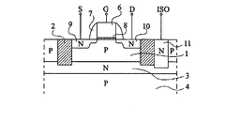
- FIG. 1is a simplified cross-section view of an example of such a memory cell.
- This cellcomprises an N-channel MOS transistor formed in a floating body region 1 laterally delimited by an isolating ring 2 and, depthwise, by an N-type layer 3 formed in a P-type substrate 4 .
- the MOS transistorcomprises, on either side of a gate region 6 surrounded with spacers 7 and resting on a gate insulator 8 , N-type source and drain regions 9 and 10 .
- Each of the source and drain regionscomprises a deeper, more heavily doped region outside of the region defined by spacers 7 and a shallower, less heavily doped region under spacers 7 .
- floating body 1In the absence of a specific action on the cell, floating body 1 is at a given voltage corresponding to the thermal equilibrium. It has been shown that positive or negative charges could be injected into this body, setting the cell to one or the other of two determined states which will be designated as 1 and 0 . According to this biasing of the substrate, the threshold voltage of the transistor modifies and states 1 and 0 can thus be distinguished.
- FIG. 1shows an N-type conductive well 11 joining buried layer 3 to enable biasing thereof.
- the biasing terminalis called ISO
- buried layer 3can be called an insulating layer.
- FIG. 2is a table illustrating the voltages to be applied to the cell in various operation modes thereof.
- Voltages VISO to be applied to buried layer 3VS to be applied to the source, VD to be applied to the drain, and VG to be applied to the gate, have more specifically been indicated.
- the conduction current of the transistor measured in these various statesdesignated as IS and expressed in microamperes while all the voltages are expressed in volts, has been indicated. More specifically, states of writing of a 1 (WR 1 ), of writing of a 0 (WR 0 ), of reading (READ), of holding or retaining (HOLD), and of erasing (ERASE) have been distinguished.
- the values given in this tableare given as an example only and correspond to a specific technology. The relative values of the various voltages and their biasings should essentially be considered.
- the given examplecorresponds to a technology in which the minimum possible dimension of a pattern is on the order of 0.12 ⁇ m, and in which a gate length on the order of 0.30 ⁇ m and a depth of STI insulation regions 2 on the order of 0.35 ⁇ m, as well as a gate oxide thickness on the order of 6 nm, have been selected.
- the main states of the cellare the following.
- the MOS transistoris set to a relatively high conduction state (currents on the order of 20 ⁇ A). This state can be established for a very short time only, for example, on the order of a few nanoseconds. At the end of this state, when all the applied voltages are brought back to zero, except the buried layer voltage which is preferably maintained at a slightly positive value, for example, 0.4 volt, the memory cell is in the state illustrated in FIG. 3A , that is, positive charges have been stored in the floating body. Once the memory cell is at the thermal equilibrium state, the charges tend, as illustrated, to narrow the space charge areas. The transistor then has a low threshold voltage, that is, in a read state in which the transistor is lightly biased to be conductive, a first current (16 ⁇ A in the illustrated example) will be observed for a given gate voltage.
- the MOS transistoris set to a slightly conductive state, the drain for example only being at a voltage on the order of 0.4 V to limit injections capable of deprogramming the transistor.
- the current flowing through transistor MOSis measured or, preferably, compared with a reference value ranging between the current values corresponding to states 1 and 0 .
- HoldingNo voltage is applied to the transistor.
- the voltage applied to buried layer 3is preferably maintained slightly positive to better block the junction between the isolated body and the buried layer in the case where the transistor is programmed at state 1 .
- the source/body (or drain/body) junctionis biased in the conductive state, which enables evacuating positive charges. Buried layer 3 remains slightly positively biased.
- the memory effect of a cell according to the present inventionis characterized by a difference between a current at state 1 and a current at state 0 for a given drain-source biasing and for a given gate voltage.
- Reference current I refis generally selected to be equal to average (I 1 +I 0 )/2 of I 1 and I 0 .
- An object of the present inventionis to improve the read sensitivity.
- the present inventionprovides a memory cell with a MOS transistor formed in a floating body region isolated on its lower surface by a junction, in which a region of the same conductivity type as the floating body region but more heavily doped than said region is arranged under the drain region of the MOS transistor.
- the drain regioncomprises a drain contact region and a more lightly doped drain extension region on the gate side, and the region of the same conductivity type as the floating body region extends under the drain contact region, adjacently thereto.
- the floating body regionhas a doping level on the order of 10 17 at./cm 3
- the region of the same conductivity type as the floating body regionis a buried region having an average doping on the order of from 5.10 17 to 10 19 at./cm 3 .
- the present inventionalso provides a method for manufacturing a cell such as mentioned hereabove in which said region of the same conductivity type as the floating body region results from an oblique implantation performed after forming of the MOS transistor gate, the orientation of the wafer with respect to the implantation direction being selected so that the gate substantially masks the implantation on the source side.
- the present inventionalso aims at an integrated circuit comprising at least a memory cell such as mentioned hereabove.
- FIG. 1shows a memory cell comprising a transistor with a floating body
- FIG. 2is a table illustrating examples of voltages applied to the cell of FIG. 1 in different states
- FIG. 3Ashows the structure of FIG. 1 in the hold state after writing of a state 1 ;
- FIG. 3Bshows the structure of FIG. 1 in the hold state after writing of a state 0 ;
- FIGS. 4A and 4Bshow two different sets of currents at state 1 and at state 0 ;
- FIG. 5is a simplified cross-section view of a memory cell according to an embodiment of the present invention.
- FIG. 6is an example of a manufacturing step of the memory cell according to the present invention.
- the inventorshave thus formed a memory cell comprising a transistor with a floating body region in which interval I 1 ⁇ I 0 is substantially unmodified with respect to a conventional cell such as that shown in FIG. 1 but in which the values of I 1 and I 0 are smaller.
- Source region 9a source contact region 9 - 1 and a source extension region 9 - 2 , more lightly doped, have been distinguished under spacer 7 .
- Region 41is preferably located under drain contact region 10 - 1 and is adjacent thereto, without rising back up in the channel region under gate 6 .
- region 41could be formed after forming of the gate and before (or after) forming of the spacers by masking half of the structure with a mask stopping on the gate and by performing an implantation of P-type dopant ions, for example, boron.
- P-type dopant ionsfor example, boron.
- region 41will be a buried region having an average doping on the order of from 5.10 17 to 10 19 at./cm 3 .
- FIG. 6Another method for forming region 41 is illustrated in FIG. 6 . It is started from a P-type substrate 4 in which an active region has been defined with shallow trenches 2 filled with an insulator. A step at which gate 6 has been formed on its gate insulator 8 and where regions 42 and 43 which will correspond to the source and drain extension regions have been formed is considered. An oblique implantation of boron atoms with an implantation power selected so that the implanted region is clearly located under regions 42 and 43 is then performed. On the drain side, a region 45 which widely extends around the drain, and which will remain around the drain even once the more heavily-doped drain regions will be implanted after forming of the spacers, is obtained.
- the oblique implantationis for the most part masked by gate 6 .
- a small area designated with reference numeral 46will optionally be implanted to the left on the drawing. However, this implantation is all the less disturbing as it will be partially erased by the heavy-dose N-type implantation performed afterwards to form the source contact region.
Landscapes
- Semiconductor Memories (AREA)
- Non-Volatile Memory (AREA)
- Dram (AREA)
Abstract
Description
- 1. Field of the Invention
- The present invention generally relates to DRAM-type memory cells with one transistor formed in a floating body or well delimited depthwise by a junction.
- 2. Discussion of the Related Art
FIG. 1 is a simplified cross-section view of an example of such a memory cell. This cell comprises an N-channel MOS transistor formed in afloating body region 1 laterally delimited by anisolating ring 2 and, depthwise, by an N-type layer 3 formed in a P-type substrate 4. The MOS transistor comprises, on either side of agate region 6 surrounded with spacers7 and resting on agate insulator 8, N-type source anddrain regions 9 and10. Each of the source and drain regions comprises a deeper, more heavily doped region outside of the region defined by spacers7 and a shallower, less heavily doped region under spacers7.- In the absence of a specific action on the cell, floating
body 1 is at a given voltage corresponding to the thermal equilibrium. It has been shown that positive or negative charges could be injected into this body, setting the cell to one or the other of two determined states which will be designated as1 and0. According to this biasing of the substrate, the threshold voltage of the transistor modifies andstates - Further,
FIG. 1 shows an N-type conductive well11 joining buriedlayer 3 to enable biasing thereof. In the drawing, the biasing terminal is called ISO, and buriedlayer 3 can be called an insulating layer. FIG. 2 is a table illustrating the voltages to be applied to the cell in various operation modes thereof. Voltages VISO to be applied to buriedlayer 3, VS to be applied to the source, VD to be applied to the drain, and VG to be applied to the gate, have more specifically been indicated. In the right-hand column, the conduction current of the transistor measured in these various states, designated as IS and expressed in microamperes while all the voltages are expressed in volts, has been indicated. More specifically, states of writing of a1 (WR1), of writing of a0 (WR0), of reading (READ), of holding or retaining (HOLD), and of erasing (ERASE) have been distinguished. The values given in this table are given as an example only and correspond to a specific technology. The relative values of the various voltages and their biasings should essentially be considered. The given example corresponds to a technology in which the minimum possible dimension of a pattern is on the order of 0.12 μm, and in which a gate length on the order of 0.30 μm and a depth ofSTI insulation regions 2 on the order of 0.35 μm, as well as a gate oxide thickness on the order of 6 nm, have been selected.- Thus, the main states of the cell are the following.
- Writing of a1 (WR1). The MOS transistor is set to a relatively high conduction state (currents on the order of 20 μA). This state can be established for a very short time only, for example, on the order of a few nanoseconds. At the end of this state, when all the applied voltages are brought back to zero, except the buried layer voltage which is preferably maintained at a slightly positive value, for example, 0.4 volt, the memory cell is in the state illustrated in
FIG. 3A , that is, positive charges have been stored in the floating body. Once the memory cell is at the thermal equilibrium state, the charges tend, as illustrated, to narrow the space charge areas. The transistor then has a low threshold voltage, that is, in a read state in which the transistor is lightly biased to be conductive, a first current (16 μA in the illustrated example) will be observed for a given gate voltage. - Writing of a0 (WR0). The transistor is off, its gate being set to a negative voltage, and its source (or its drain) is also set to a negative voltage, whereby the positive charges possibly present in the substrate are eliminated and negative charges are injected after the setting to the conductive state of the body-source or body-drain diode. At the end of this state, as illustrated in
FIG. 3B , the space charge areas tend to widen, which results in an increase in the transistor threshold voltage. Thus, in read conditions in which the transistor is lightly biased to the conductive state, a current lower than the current at state1 (3 μA instead of 16 μA in the illustrated example) is obtained for a same 1.2-V gate voltage as that considered in the previous case. - Reading (READ). The MOS transistor is set to a slightly conductive state, the drain for example only being at a voltage on the order of 0.4 V to limit injections capable of deprogramming the transistor. The current flowing through transistor MOS is measured or, preferably, compared with a reference value ranging between the current values corresponding to
states - Holding (HOLD). No voltage is applied to the transistor. The voltage applied to buried
layer 3 is preferably maintained slightly positive to better block the junction between the isolated body and the buried layer in the case where the transistor is programmed atstate 1. - Erasing (ERASE). The source/body (or drain/body) junction is biased in the conductive state, which enables evacuating positive charges. Buried
layer 3 remains slightly positively biased. - Thus, as discussed previously, the memory effect of a cell according to the present invention is characterized by a difference between a current at
state 1 and a current atstate 0 for a given drain-source biasing and for a given gate voltage. - Generally, during the read phase, the detected current corresponding to a state1 (I1) or to a state0 (I0) is compared with a reference current Iref. Reference current Irefis generally selected to be equal to average (I1+I0)/2 of I1 and I0. However, given that there is a dispersion from one cell to another on the values of I1 and I0 according to the technology and that, further, values I0 and I1 are likely to vary, especially according to the cell use duration, the reading risks being tainted with error.
- An object of the present invention is to improve the read sensitivity.
- To achieve this and other objects, the present invention provides a memory cell with a MOS transistor formed in a floating body region isolated on its lower surface by a junction, in which a region of the same conductivity type as the floating body region but more heavily doped than said region is arranged under the drain region of the MOS transistor.
- According to an embodiment of the present invention, the drain region comprises a drain contact region and a more lightly doped drain extension region on the gate side, and the region of the same conductivity type as the floating body region extends under the drain contact region, adjacently thereto.
- According to an embodiment of the present invention, the floating body region has a doping level on the order of 1017at./cm3, and the region of the same conductivity type as the floating body region is a buried region having an average doping on the order of from 5.1017to 1019at./cm3.
- The present invention also provides a method for manufacturing a cell such as mentioned hereabove in which said region of the same conductivity type as the floating body region results from an oblique implantation performed after forming of the MOS transistor gate, the orientation of the wafer with respect to the implantation direction being selected so that the gate substantially masks the implantation on the source side.
- The present invention also aims at an integrated circuit comprising at least a memory cell such as mentioned hereabove.
- The foregoing and other objects, features, and advantages, of the present invention will be discussed in detail in the following non-limiting description of specific embodiments in connection with the accompanying drawings.
FIG. 1 shows a memory cell comprising a transistor with a floating body;FIG. 2 is a table illustrating examples of voltages applied to the cell ofFIG. 1 in different states;FIG. 3A shows the structure ofFIG. 1 in the hold state after writing of astate 1;FIG. 3B shows the structure ofFIG. 1 in the hold state after writing of astate 0;FIGS. 4A and 4B show two different sets of currents atstate 1 and atstate 0;FIG. 5 is a simplified cross-section view of a memory cell according to an embodiment of the present invention; andFIG. 6 is an example of a manufacturing step of the memory cell according to the present invention.- As usual in the representation of integrated circuits, the various cross-section views are not drawn to scale.
- Statistic studies performed on cell models show that the read error risk (confusion of a1 and of a0 or non-detection of a1 or of a0) decreases, for a given difference I1−I0, along with the average value of I1+I0, that is, along with the value of Iref. Thus, the risk of a read error is smaller in the case of
FIG. 4B than in the case ofFIG. 4A . - The inventors have thus formed a memory cell comprising a transistor with a floating body region in which interval I1−I0 is substantially unmodified with respect to a conventional cell such as that shown in
FIG. 1 but in which the values of I1 and I0 are smaller. - The inventors have shown that this result is obtained when the doping of floating
body region 1 under the drain region is increased. Thus, the inventors provide, as shown inFIG. 5 , forming under drain region10 a P-type region 41 more heavily-doped than the rest of the floating region. Experience has shown that this would provide satisfactory results, the read currents atstate 0 and atstate 1 being both decreased by a few microamperes. An explanation of this result is that, due to the heavier doping of the P-type region under the drain, the space charge area (not shown) extends more into the N-type drain region. As a result, the effective channel width between source and drain increases and thus, for a given gate voltage, the read current decreases. - It should further be noted that the representation of more heavily-doped
region 41 is purely for illustration purposes, the extent of this area and its rise to the drain extension region depending on the implantation and anneal conditions. - Same reference numerals as in
FIG. 4 have been used inFIG. 5 . However, in source region9, a source contact region9-1 and a source extension region9-2, more lightly doped, have been distinguished under spacer7. Similarly, a drain contact region10-1 and a more lightly-doped drain extension region10-2 under spacer7 have been distinguished underdrain region 10.Region 41 is preferably located under drain contact region10-1 and is adjacent thereto, without rising back up in the channel region undergate 6. - It will be within the abilities of those skilled in the art to manufacture a structure of the type in
FIG. 5 . For example,region 41 could be formed after forming of the gate and before (or after) forming of the spacers by masking half of the structure with a mask stopping on the gate and by performing an implantation of P-type dopant ions, for example, boron. In the case where floatingbody region 1 has a doping level on the order of 1017at./cm3,region 41 will be a buried region having an average doping on the order of from 5.1017to 1019at./cm3. - Another method for forming
region 41 is illustrated inFIG. 6 . It is started from a P-type substrate 4 in which an active region has been defined withshallow trenches 2 filled with an insulator. A step at whichgate 6 has been formed on itsgate insulator 8 and whereregions 42 and43 which will correspond to the source and drain extension regions have been formed is considered. An oblique implantation of boron atoms with an implantation power selected so that the implanted region is clearly located underregions 42 and43 is then performed. On the drain side, aregion 45 which widely extends around the drain, and which will remain around the drain even once the more heavily-doped drain regions will be implanted after forming of the spacers, is obtained. On the source side, the oblique implantation is for the most part masked bygate 6. A small area designated withreference numeral 46 will optionally be implanted to the left on the drawing. However, this implantation is all the less disturbing as it will be partially erased by the heavy-dose N-type implantation performed afterwards to form the source contact region. - The present invention is likely to have various alterations, modifications, and improvements which will occur to those skilled in the art. In particular, the various materials used and the indicated dimensions may be modified according to the technology which is used, provided that the described functions are achieved.
- Such alterations, modifications, and improvements are intended to be part of this disclosure, and are intended to be within the spirit and the scope of the present invention. Accordingly, the foregoing description is by way of example only and is not intended to be limiting. The present invention is limited only as defined in the following claims and the equivalents thereto.
Claims (5)
Applications Claiming Priority (3)
| Application Number | Priority Date | Filing Date | Title |
|---|---|---|---|
| FR0552307AFR2889356A1 (en) | 2005-07-26 | 2005-07-26 | MEMORY CELL HAS AN INSULATED BODY TRANSISTOR WITH ENHANCED READING SENSITIVITY |
| FR05/52307 | 2005-07-26 | ||
| FR0552307 | 2005-07-26 |
Publications (2)
| Publication Number | Publication Date |
|---|---|
| US20070023809A1true US20070023809A1 (en) | 2007-02-01 |
| US7709875B2 US7709875B2 (en) | 2010-05-04 |
Family
ID=36123557
Family Applications (1)
| Application Number | Title | Priority Date | Filing Date |
|---|---|---|---|
| US11/492,706Active2027-03-25US7709875B2 (en) | 2005-07-26 | 2006-07-25 | Memory cell comprising one MOS transistor with an isolated body having an improved read sensitivity |
Country Status (4)
| Country | Link |
|---|---|
| US (1) | US7709875B2 (en) |
| EP (1) | EP1748493A1 (en) |
| JP (1) | JP2007036257A (en) |
| FR (1) | FR2889356A1 (en) |
Cited By (12)
| Publication number | Priority date | Publication date | Assignee | Title |
|---|---|---|---|---|
| US20090022003A1 (en)* | 2007-07-20 | 2009-01-22 | Song Ki-Whan | Memory cell structures, memory arrays, memory devices, memory controllers, and memory systems, and methods of manufacturing and operating the same |
| US20090097332A1 (en)* | 2007-10-10 | 2009-04-16 | Samsung Electronics Co., Ltd. | Semiconductor memory device |
| US20090278194A1 (en)* | 2008-05-06 | 2009-11-12 | Nam-Kyun Tak | Capacitorless one-transistor semiconductor memory device having improved data retention abilities and operation characteristics |
| US20100149886A1 (en)* | 2008-12-17 | 2010-06-17 | Samsung Electronics Co., Ltd. | Semiconductor memory device and method for operating the same |
| US20100159650A1 (en)* | 2008-12-18 | 2010-06-24 | Song Ho-Ju | Methods of fabricating semiconductor device having capacitorless one-transistor memory cell |
| US7924644B2 (en) | 2008-01-03 | 2011-04-12 | Samsung Electronics Co., Ltd. | Semiconductor memory device including floating body transistor memory cell array and method of operating the same |
| CN102437123A (en)* | 2011-08-17 | 2012-05-02 | 上海华力微电子有限公司 | Implantation method and structure capable of enhancing writing speed of floating body dynamic random access memory unit |
| US20180158912A1 (en)* | 2015-04-29 | 2018-06-07 | Jin-Woo Han | MOSFET and Memory Cell Having Improved Drain Current Through Back Bias Application |
| US10181471B2 (en) | 2012-02-16 | 2019-01-15 | Zeno Semiconductor, Inc. | Memory cell comprising first and second transistors and methods of operating |
| US11201215B2 (en) | 2015-04-29 | 2021-12-14 | Zeno Semiconductor, Inc. | MOSFET and memory cell having improved drain current through back bias application |
| US11908899B2 (en) | 2009-02-20 | 2024-02-20 | Zeno Semiconductor, Inc. | MOSFET and memory cell having improved drain current through back bias application |
| US11974425B2 (en) | 2012-02-16 | 2024-04-30 | Zeno Semiconductor, Inc. | Memory cell comprising first and second transistors and methods of operating |
Families Citing this family (2)
| Publication number | Priority date | Publication date | Assignee | Title |
|---|---|---|---|---|
| KR101357304B1 (en) | 2007-09-11 | 2014-01-28 | 삼성전자주식회사 | Capacitorless DRAM and methods of manufacturing and operating the same |
| TWI787498B (en)* | 2018-04-18 | 2022-12-21 | 美商季諾半導體股份有限公司 | A memory device comprising an electrically floating body transistor |
Citations (9)
| Publication number | Priority date | Publication date | Assignee | Title |
|---|---|---|---|---|
| US5698869A (en)* | 1994-09-13 | 1997-12-16 | Kabushiki Kaisha Toshiba | Insulated-gate transistor having narrow-bandgap-source |
| US6213869B1 (en)* | 1999-05-10 | 2001-04-10 | Advanced Micro Devices, Inc. | MOSFET-type device with higher driver current and lower steady state power dissipation |
| US6333217B1 (en)* | 1999-05-14 | 2001-12-25 | Matsushita Electric Industrial Co., Ltd. | Method of forming MOSFET with channel, extension and pocket implants |
| US20020050614A1 (en)* | 1999-09-02 | 2002-05-02 | Sreenath Unnikrishnan | Body-tied-to-source partially depleted SOI MOSFET |
| US20020074612A1 (en)* | 2000-03-31 | 2002-06-20 | National Semiconductor Corporation | Fabrication of field-effect transistor for alleviating short-channel effects and/or reducing junction capacitance |
| US20040089890A1 (en)* | 2002-11-08 | 2004-05-13 | Burnett James D. | One transistor DRAM cell structure and method for forming |
| US20040113193A1 (en)* | 2001-01-12 | 2004-06-17 | Olivier Menut | Integrated circuit and method for making the same |
| US20040166637A1 (en)* | 2000-05-30 | 2004-08-26 | Hiroyasu Ito | Manufacturing method of semiconductor device |
| US20060067126A1 (en)* | 2004-09-30 | 2006-03-30 | Tang Stephen H | Floating-body memory cell write |
- 2005
- 2005-07-26FRFR0552307Apatent/FR2889356A1/ennot_activeWithdrawn
- 2006
- 2006-07-21EPEP06117667Apatent/EP1748493A1/ennot_activeWithdrawn
- 2006-07-25USUS11/492,706patent/US7709875B2/enactiveActive
- 2006-07-26JPJP2006203309Apatent/JP2007036257A/enactivePending
Patent Citations (11)
| Publication number | Priority date | Publication date | Assignee | Title |
|---|---|---|---|---|
| US5698869A (en)* | 1994-09-13 | 1997-12-16 | Kabushiki Kaisha Toshiba | Insulated-gate transistor having narrow-bandgap-source |
| US6213869B1 (en)* | 1999-05-10 | 2001-04-10 | Advanced Micro Devices, Inc. | MOSFET-type device with higher driver current and lower steady state power dissipation |
| US6333217B1 (en)* | 1999-05-14 | 2001-12-25 | Matsushita Electric Industrial Co., Ltd. | Method of forming MOSFET with channel, extension and pocket implants |
| US20020034865A1 (en)* | 1999-05-14 | 2002-03-21 | Hiroyuki Umimoto | Semiconductor device and method of fabricating the same |
| US20020050614A1 (en)* | 1999-09-02 | 2002-05-02 | Sreenath Unnikrishnan | Body-tied-to-source partially depleted SOI MOSFET |
| US20020074612A1 (en)* | 2000-03-31 | 2002-06-20 | National Semiconductor Corporation | Fabrication of field-effect transistor for alleviating short-channel effects and/or reducing junction capacitance |
| US6548842B1 (en)* | 2000-03-31 | 2003-04-15 | National Semiconductor Corporation | Field-effect transistor for alleviating short-channel effects |
| US20040166637A1 (en)* | 2000-05-30 | 2004-08-26 | Hiroyasu Ito | Manufacturing method of semiconductor device |
| US20040113193A1 (en)* | 2001-01-12 | 2004-06-17 | Olivier Menut | Integrated circuit and method for making the same |
| US20040089890A1 (en)* | 2002-11-08 | 2004-05-13 | Burnett James D. | One transistor DRAM cell structure and method for forming |
| US20060067126A1 (en)* | 2004-09-30 | 2006-03-30 | Tang Stephen H | Floating-body memory cell write |
Cited By (20)
| Publication number | Priority date | Publication date | Assignee | Title |
|---|---|---|---|---|
| US20090022003A1 (en)* | 2007-07-20 | 2009-01-22 | Song Ki-Whan | Memory cell structures, memory arrays, memory devices, memory controllers, and memory systems, and methods of manufacturing and operating the same |
| US7969808B2 (en) | 2007-07-20 | 2011-06-28 | Samsung Electronics Co., Ltd. | Memory cell structures, memory arrays, memory devices, memory controllers, and memory systems, and methods of manufacturing and operating the same |
| US20090097332A1 (en)* | 2007-10-10 | 2009-04-16 | Samsung Electronics Co., Ltd. | Semiconductor memory device |
| US7944759B2 (en) | 2007-10-10 | 2011-05-17 | Samsung Electronics Co., Ltd. | Semiconductor memory device including floating body transistor |
| US7924644B2 (en) | 2008-01-03 | 2011-04-12 | Samsung Electronics Co., Ltd. | Semiconductor memory device including floating body transistor memory cell array and method of operating the same |
| US8134202B2 (en) | 2008-05-06 | 2012-03-13 | Samsung Electronics Co., Ltd. | Capacitorless one-transistor semiconductor memory device having improved data retention abilities and operation characteristics |
| US20090278194A1 (en)* | 2008-05-06 | 2009-11-12 | Nam-Kyun Tak | Capacitorless one-transistor semiconductor memory device having improved data retention abilities and operation characteristics |
| US20100149886A1 (en)* | 2008-12-17 | 2010-06-17 | Samsung Electronics Co., Ltd. | Semiconductor memory device and method for operating the same |
| US8054693B2 (en) | 2008-12-17 | 2011-11-08 | Samsung Electronics Co., Ltd. | Capacitorless dynamic memory device capable of performing data read/restoration and method for operating the same |
| US20100159650A1 (en)* | 2008-12-18 | 2010-06-24 | Song Ho-Ju | Methods of fabricating semiconductor device having capacitorless one-transistor memory cell |
| US8039325B2 (en) | 2008-12-18 | 2011-10-18 | Samsung Electronics Co., Ltd. | Methods of fabricating semiconductor device having capacitorless one-transistor memory cell |
| US11908899B2 (en) | 2009-02-20 | 2024-02-20 | Zeno Semiconductor, Inc. | MOSFET and memory cell having improved drain current through back bias application |
| CN102437123A (en)* | 2011-08-17 | 2012-05-02 | 上海华力微电子有限公司 | Implantation method and structure capable of enhancing writing speed of floating body dynamic random access memory unit |
| US10797055B2 (en) | 2012-02-16 | 2020-10-06 | Zeno Semiconductor, Inc. | Memory cell comprising first and second transistors and methods of operating |
| US10181471B2 (en) | 2012-02-16 | 2019-01-15 | Zeno Semiconductor, Inc. | Memory cell comprising first and second transistors and methods of operating |
| US11348922B2 (en) | 2012-02-16 | 2022-05-31 | Zeno Semiconductor, Inc. | Memory cell comprising first and second transistors and methods of operating |
| US11974425B2 (en) | 2012-02-16 | 2024-04-30 | Zeno Semiconductor, Inc. | Memory cell comprising first and second transistors and methods of operating |
| US10553683B2 (en)* | 2015-04-29 | 2020-02-04 | Zeno Semiconductor, Inc. | MOSFET and memory cell having improved drain current through back bias application |
| US11201215B2 (en) | 2015-04-29 | 2021-12-14 | Zeno Semiconductor, Inc. | MOSFET and memory cell having improved drain current through back bias application |
| US20180158912A1 (en)* | 2015-04-29 | 2018-06-07 | Jin-Woo Han | MOSFET and Memory Cell Having Improved Drain Current Through Back Bias Application |
Also Published As
| Publication number | Publication date |
|---|---|
| US7709875B2 (en) | 2010-05-04 |
| EP1748493A8 (en) | 2007-08-15 |
| JP2007036257A (en) | 2007-02-08 |
| EP1748493A1 (en) | 2007-01-31 |
| FR2889356A1 (en) | 2007-02-02 |
Similar Documents
| Publication | Publication Date | Title |
|---|---|---|
| US7709875B2 (en) | Memory cell comprising one MOS transistor with an isolated body having an improved read sensitivity | |
| US7541636B2 (en) | Memory cell comprising one MOS transistor with an isolated body having a reinforced memory effect | |
| US10079316B2 (en) | Split gate embedded memory technology and method of manufacturing thereof | |
| KR100459872B1 (en) | Buried channel transistor having trench gate and Method of manufacturing the same | |
| US20070001165A1 (en) | Memory cell comprising one MOS transistor with an isolated body having a prolonged memory effect | |
| US20100155858A1 (en) | Asymmetric extension device | |
| US20040232493A1 (en) | Integrated circuits having channel regions with different ion levels | |
| US8466505B2 (en) | Multi-level flash memory cell capable of fast programming | |
| CN100466264C (en) | Memory cell and method of forming a memory cell | |
| US20020136058A1 (en) | Channel write/erase flash memory cell and its manufacturing method | |
| US8044455B2 (en) | Semiconductor device and method of manufacturing the same | |
| US20150221660A1 (en) | Semiconductor memory device and method of manufacturing the same | |
| JPH11330280A (en) | Method of manufacturing flash memory-cell structure by channel erase / write and method of operating the same | |
| KR101552921B1 (en) | Method of manufacturing non volatile memory device | |
| KR100549578B1 (en) | MOOS transistor manufacturing method | |
| JP4854955B2 (en) | Semiconductor device and manufacturing method thereof | |
| US6614074B2 (en) | Grooved planar DRAM transfer device using buried pocket | |
| US20170229540A1 (en) | Non-volatile memory device having reduced drain and read disturbances | |
| CN110047833B (en) | Memory, working method and forming method thereof | |
| US20030230785A1 (en) | Semiconductor device having silicon oxide film | |
| US8138541B2 (en) | Memory cells | |
| US6703662B1 (en) | Semiconductor device and manufacturing method thereof | |
| JPH0621447A (en) | Short channel field effect transistor | |
| Lo et al. | Study of the walk-out effect of junction breakdown instability of the high-voltage depletion-mode N-channel MOSFET for NAND flash peripheral device and an efficient layout solution | |
| US10991707B2 (en) | Semiconductor device and method for fabricating semiconductor device |
Legal Events
| Date | Code | Title | Description |
|---|---|---|---|
| AS | Assignment | Owner name:STMICROELECTRONICS CROLLES 2 SAS,FRANCE Free format text:ASSIGNMENT OF ASSIGNORS INTEREST;ASSIGNORS:VILLARET, ALEXANDRE;MAZOYER, PASCALE;RANICA, ROSSELLA;REEL/FRAME:018214/0698 Effective date:20060810 Owner name:STMICROELECTRONICS CROLLES 2 SAS, FRANCE Free format text:ASSIGNMENT OF ASSIGNORS INTEREST;ASSIGNORS:VILLARET, ALEXANDRE;MAZOYER, PASCALE;RANICA, ROSSELLA;REEL/FRAME:018214/0698 Effective date:20060810 | |
| STCF | Information on status: patent grant | Free format text:PATENTED CASE | |
| AS | Assignment | Owner name:STMICROELECTRONICS (CROLLES 2) SAS, FRANCE Free format text:CORRECTIVE ASSIGNMENT TO CORRECT THE ASSIGNEE'S NAME PREVIOUSLY RECORDED ON REEL 018214 FRAME 0698. ASSIGNOR(S) HEREBY CONFIRMS THE ADDITION OF PARENTHESIS AROUND CROLLES 2 IN THE NAME STMICROELECTRONICS (CROLLES 2) SAS;ASSIGNORS:VILLARET, ALEXANDRE;MAZOYER, PASCALE;RANICA, ROSSELLA;REEL/FRAME:027269/0926 Effective date:20060810 | |
| CC | Certificate of correction | ||
| FPAY | Fee payment | Year of fee payment:4 | |
| MAFP | Maintenance fee payment | Free format text:PAYMENT OF MAINTENANCE FEE, 8TH YEAR, LARGE ENTITY (ORIGINAL EVENT CODE: M1552) Year of fee payment:8 | |
| MAFP | Maintenance fee payment | Free format text:PAYMENT OF MAINTENANCE FEE, 12TH YEAR, LARGE ENTITY (ORIGINAL EVENT CODE: M1553); ENTITY STATUS OF PATENT OWNER: LARGE ENTITY Year of fee payment:12 |