US20070020885A1 - Tube Formed of Bonded Silicon Staves - Google Patents
Tube Formed of Bonded Silicon StavesDownload PDFInfo
- Publication number
- US20070020885A1 US20070020885A1US11/532,661US53266106AUS2007020885A1US 20070020885 A1US20070020885 A1US 20070020885A1US 53266106 AUS53266106 AUS 53266106AUS 2007020885 A1US2007020885 A1US 2007020885A1
- Authority
- US
- United States
- Prior art keywords
- silicon
- staves
- tube
- tower
- nitride
- Prior art date
- Legal status (The legal status is an assumption and is not a legal conclusion. Google has not performed a legal analysis and makes no representation as to the accuracy of the status listed.)
- Granted
Links
- XUIMIQQOPSSXEZ-UHFFFAOYSA-NSiliconChemical compound[Si]XUIMIQQOPSSXEZ-UHFFFAOYSA-N0.000titleclaimsabstractdescription140
- 229910052710siliconInorganic materials0.000titleclaimsabstractdescription122
- 239000010703siliconSubstances0.000titleclaimsabstractdescription122
- VYPSYNLAJGMNEJ-UHFFFAOYSA-NSilicium dioxideChemical compoundO=[Si]=OVYPSYNLAJGMNEJ-UHFFFAOYSA-N0.000claimsabstractdescription48
- 238000000034methodMethods0.000claimsabstractdescription33
- 229910021420polycrystalline siliconInorganic materials0.000claimsabstractdescription26
- 229920005591polysiliconPolymers0.000claimsabstractdescription25
- 239000000377silicon dioxideSubstances0.000claimsabstractdescription9
- 239000011521glassSubstances0.000claimsdescription9
- 210000002105tongueAnatomy0.000claimsdescription4
- 239000007767bonding agentSubstances0.000claimsdescription3
- 238000005304joiningMethods0.000claimsdescription3
- 229910052581Si3N4Inorganic materials0.000abstractdescription33
- HQVNEWCFYHHQES-UHFFFAOYSA-Nsilicon nitrideChemical compoundN12[Si]34N5[Si]62N3[Si]51N64HQVNEWCFYHHQES-UHFFFAOYSA-N0.000abstractdescription31
- 238000005229chemical vapour depositionMethods0.000abstractdescription26
- 238000000151depositionMethods0.000abstractdescription26
- 150000004767nitridesChemical class0.000abstractdescription24
- 230000008021depositionEffects0.000abstractdescription23
- 238000002230thermal chemical vapour depositionMethods0.000abstractdescription21
- 239000000463materialSubstances0.000abstractdescription20
- 239000011324beadSubstances0.000abstractdescription9
- 239000005368silicate glassSubstances0.000abstractdescription8
- 239000000758substrateSubstances0.000abstractdescription5
- 238000001125extrusionMethods0.000abstractdescription4
- 230000002401inhibitory effectEffects0.000abstract1
- 235000012431wafersNutrition0.000description56
- 239000010410layerSubstances0.000description26
- 239000010453quartzSubstances0.000description25
- 235000012239silicon dioxideNutrition0.000description25
- 239000002245particleSubstances0.000description22
- 238000004519manufacturing processMethods0.000description14
- 238000004381surface treatmentMethods0.000description12
- 238000005422blastingMethods0.000description10
- HBMJWWWQQXIZIP-UHFFFAOYSA-Nsilicon carbideChemical compound[Si+]#[C-]HBMJWWWQQXIZIP-UHFFFAOYSA-N0.000description10
- 229910010271silicon carbideInorganic materials0.000description10
- 239000007789gasSubstances0.000description9
- 239000002243precursorSubstances0.000description9
- QGZKDVFQNNGYKY-UHFFFAOYSA-NAmmoniaChemical compoundNQGZKDVFQNNGYKY-UHFFFAOYSA-N0.000description7
- 239000002184metalSubstances0.000description6
- 229910052751metalInorganic materials0.000description6
- 239000005046ChlorosilaneSubstances0.000description5
- BLRPTPMANUNPDV-UHFFFAOYSA-NSilaneChemical compound[SiH4]BLRPTPMANUNPDV-UHFFFAOYSA-N0.000description5
- KOPOQZFJUQMUML-UHFFFAOYSA-NchlorosilaneChemical compoundCl[SiH3]KOPOQZFJUQMUML-UHFFFAOYSA-N0.000description5
- 238000005516engineering processMethods0.000description5
- 239000000203mixtureSubstances0.000description5
- 229910000077silaneInorganic materials0.000description5
- IJGRMHOSHXDMSA-UHFFFAOYSA-NAtomic nitrogenChemical compoundN#NIJGRMHOSHXDMSA-UHFFFAOYSA-N0.000description4
- KRHYYFGTRYWZRS-UHFFFAOYSA-NFluoraneChemical compoundFKRHYYFGTRYWZRS-UHFFFAOYSA-N0.000description4
- 238000000137annealingMethods0.000description4
- 238000004140cleaningMethods0.000description4
- 150000002739metalsChemical class0.000description4
- 239000004065semiconductorSubstances0.000description4
- 229910021529ammoniaInorganic materials0.000description3
- 239000000356contaminantSubstances0.000description3
- 238000003754machiningMethods0.000description3
- 230000003746surface roughnessEffects0.000description3
- CURLTUGMZLYLDI-UHFFFAOYSA-NCarbon dioxideChemical compoundO=C=OCURLTUGMZLYLDI-UHFFFAOYSA-N0.000description2
- 239000006117anti-reflective coatingSubstances0.000description2
- QVGXLLKOCUKJST-UHFFFAOYSA-Natomic oxygenChemical compound[O]QVGXLLKOCUKJST-UHFFFAOYSA-N0.000description2
- 238000006243chemical reactionMethods0.000description2
- 239000011248coating agentSubstances0.000description2
- 238000000576coating methodMethods0.000description2
- 238000011109contaminationMethods0.000description2
- 239000002019doping agentSubstances0.000description2
- 238000009472formulationMethods0.000description2
- 229910052732germaniumInorganic materials0.000description2
- GNPVGFCGXDBREM-UHFFFAOYSA-Ngermanium atomChemical compound[Ge]GNPVGFCGXDBREM-UHFFFAOYSA-N0.000description2
- 238000010438heat treatmentMethods0.000description2
- 230000007062hydrolysisEffects0.000description2
- 238000006460hydrolysis reactionMethods0.000description2
- 239000012535impuritySubstances0.000description2
- 238000004518low pressure chemical vapour depositionMethods0.000description2
- 229910052757nitrogenInorganic materials0.000description2
- NJPPVKZQTLUDBO-UHFFFAOYSA-NnovaluronChemical compoundC1=C(Cl)C(OC(F)(F)C(OC(F)(F)F)F)=CC=C1NC(=O)NC(=O)C1=C(F)C=CC=C1FNJPPVKZQTLUDBO-UHFFFAOYSA-N0.000description2
- 230000003647oxidationEffects0.000description2
- 238000007254oxidation reactionMethods0.000description2
- 239000001301oxygenSubstances0.000description2
- 229910052760oxygenInorganic materials0.000description2
- 238000005268plasma chemical vapour depositionMethods0.000description2
- 238000000623plasma-assisted chemical vapour depositionMethods0.000description2
- 238000002203pretreatmentMethods0.000description2
- 238000005245sinteringMethods0.000description2
- 238000003466weldingMethods0.000description2
- NLXLAEXVIDQMFP-UHFFFAOYSA-NAmmonia chlorideChemical compound[NH4+].[Cl-]NLXLAEXVIDQMFP-UHFFFAOYSA-N0.000description1
- OKTJSMMVPCPJKN-UHFFFAOYSA-NCarbonChemical compound[C]OKTJSMMVPCPJKN-UHFFFAOYSA-N0.000description1
- UFHFLCQGNIYNRP-UHFFFAOYSA-NHydrogenChemical compound[H][H]UFHFLCQGNIYNRP-UHFFFAOYSA-N0.000description1
- GRYLNZFGIOXLOG-UHFFFAOYSA-NNitric acidChemical compoundO[N+]([O-])=OGRYLNZFGIOXLOG-UHFFFAOYSA-N0.000description1
- 229910019142PO4Inorganic materials0.000description1
- 229910004205SiNXInorganic materials0.000description1
- 239000002253acidSubstances0.000description1
- 229910021486amorphous silicon dioxideInorganic materials0.000description1
- 238000001505atmospheric-pressure chemical vapour depositionMethods0.000description1
- 229910052799carbonInorganic materials0.000description1
- 229910002092carbon dioxideInorganic materials0.000description1
- 239000001569carbon dioxideSubstances0.000description1
- 239000000919ceramicSubstances0.000description1
- 239000007795chemical reaction productSubstances0.000description1
- 229910052681coesiteInorganic materials0.000description1
- 150000001875compoundsChemical class0.000description1
- 229910052906cristobaliteInorganic materials0.000description1
- 230000003247decreasing effectEffects0.000description1
- 230000003111delayed effectEffects0.000description1
- 230000002939deleterious effectEffects0.000description1
- 238000005137deposition processMethods0.000description1
- 239000003599detergentSubstances0.000description1
- 238000009792diffusion processMethods0.000description1
- 238000005530etchingMethods0.000description1
- 238000011049fillingMethods0.000description1
- 229910000078germaneInorganic materials0.000description1
- 238000000227grindingMethods0.000description1
- 239000001257hydrogenSubstances0.000description1
- 229910052739hydrogenInorganic materials0.000description1
- 230000001939inductive effectEffects0.000description1
- 238000012423maintenanceMethods0.000description1
- 230000008018meltingEffects0.000description1
- 238000002844meltingMethods0.000description1
- 229910017604nitric acidInorganic materials0.000description1
- 229910000069nitrogen hydrideInorganic materials0.000description1
- 230000000149penetrating effectEffects0.000description1
- NBIIXXVUZAFLBC-UHFFFAOYSA-KphosphateChemical compound[O-]P([O-])([O-])=ONBIIXXVUZAFLBC-UHFFFAOYSA-K0.000description1
- 239000010452phosphateSubstances0.000description1
- 238000001020plasma etchingMethods0.000description1
- 238000005498polishingMethods0.000description1
- 230000003449preventive effectEffects0.000description1
- 239000011253protective coatingSubstances0.000description1
- 239000000376reactantSubstances0.000description1
- 238000009877renderingMethods0.000description1
- 238000007788rougheningMethods0.000description1
- 238000005488sandblastingMethods0.000description1
- 229910052594sapphireInorganic materials0.000description1
- 239000010980sapphireSubstances0.000description1
- 239000002210silicon-based materialSubstances0.000description1
- 239000011856silicon-based particleSubstances0.000description1
- 229910052682stishoviteInorganic materials0.000description1
- 239000000126substanceSubstances0.000description1
- 239000002344surface layerSubstances0.000description1
- 238000010301surface-oxidation reactionMethods0.000description1
- 229910052905tridymiteInorganic materials0.000description1
- 238000005406washingMethods0.000description1
- XLYOFNOQVPJJNP-UHFFFAOYSA-NwaterChemical compoundOXLYOFNOQVPJJNP-UHFFFAOYSA-N0.000description1
Images


Classifications
- H—ELECTRICITY
- H01—ELECTRIC ELEMENTS
- H01L—SEMICONDUCTOR DEVICES NOT COVERED BY CLASS H10
- H01L21/00—Processes or apparatus adapted for the manufacture or treatment of semiconductor or solid state devices or of parts thereof
- H01L21/67—Apparatus specially adapted for handling semiconductor or electric solid state devices during manufacture or treatment thereof; Apparatus specially adapted for handling wafers during manufacture or treatment of semiconductor or electric solid state devices or components ; Apparatus not specifically provided for elsewhere
- H01L21/673—Apparatus specially adapted for handling semiconductor or electric solid state devices during manufacture or treatment thereof; Apparatus specially adapted for handling wafers during manufacture or treatment of semiconductor or electric solid state devices or components ; Apparatus not specifically provided for elsewhere using specially adapted carriers or holders; Fixing the workpieces on such carriers or holders
- H01L21/67303—Vertical boat type carrier whereby the substrates are horizontally supported, e.g. comprising rod-shaped elements
- H01L21/67306—Vertical boat type carrier whereby the substrates are horizontally supported, e.g. comprising rod-shaped elements characterized by a material, a roughness, a coating or the like
- C—CHEMISTRY; METALLURGY
- C23—COATING METALLIC MATERIAL; COATING MATERIAL WITH METALLIC MATERIAL; CHEMICAL SURFACE TREATMENT; DIFFUSION TREATMENT OF METALLIC MATERIAL; COATING BY VACUUM EVAPORATION, BY SPUTTERING, BY ION IMPLANTATION OR BY CHEMICAL VAPOUR DEPOSITION, IN GENERAL; INHIBITING CORROSION OF METALLIC MATERIAL OR INCRUSTATION IN GENERAL
- C23C—COATING METALLIC MATERIAL; COATING MATERIAL WITH METALLIC MATERIAL; SURFACE TREATMENT OF METALLIC MATERIAL BY DIFFUSION INTO THE SURFACE, BY CHEMICAL CONVERSION OR SUBSTITUTION; COATING BY VACUUM EVAPORATION, BY SPUTTERING, BY ION IMPLANTATION OR BY CHEMICAL VAPOUR DEPOSITION, IN GENERAL
- C23C16/00—Chemical coating by decomposition of gaseous compounds, without leaving reaction products of surface material in the coating, i.e. chemical vapour deposition [CVD] processes
- C23C16/44—Chemical coating by decomposition of gaseous compounds, without leaving reaction products of surface material in the coating, i.e. chemical vapour deposition [CVD] processes characterised by the method of coating
- C23C16/4401—Means for minimising impurities, e.g. dust, moisture or residual gas, in the reaction chamber
- C23C16/4404—Coatings or surface treatment on the inside of the reaction chamber or on parts thereof
- C—CHEMISTRY; METALLURGY
- C23—COATING METALLIC MATERIAL; COATING MATERIAL WITH METALLIC MATERIAL; CHEMICAL SURFACE TREATMENT; DIFFUSION TREATMENT OF METALLIC MATERIAL; COATING BY VACUUM EVAPORATION, BY SPUTTERING, BY ION IMPLANTATION OR BY CHEMICAL VAPOUR DEPOSITION, IN GENERAL; INHIBITING CORROSION OF METALLIC MATERIAL OR INCRUSTATION IN GENERAL
- C23C—COATING METALLIC MATERIAL; COATING MATERIAL WITH METALLIC MATERIAL; SURFACE TREATMENT OF METALLIC MATERIAL BY DIFFUSION INTO THE SURFACE, BY CHEMICAL CONVERSION OR SUBSTITUTION; COATING BY VACUUM EVAPORATION, BY SPUTTERING, BY ION IMPLANTATION OR BY CHEMICAL VAPOUR DEPOSITION, IN GENERAL
- C23C16/00—Chemical coating by decomposition of gaseous compounds, without leaving reaction products of surface material in the coating, i.e. chemical vapour deposition [CVD] processes
- C23C16/44—Chemical coating by decomposition of gaseous compounds, without leaving reaction products of surface material in the coating, i.e. chemical vapour deposition [CVD] processes characterised by the method of coating
- C23C16/458—Chemical coating by decomposition of gaseous compounds, without leaving reaction products of surface material in the coating, i.e. chemical vapour deposition [CVD] processes characterised by the method of coating characterised by the method used for supporting substrates in the reaction chamber
- C23C16/4581—Chemical coating by decomposition of gaseous compounds, without leaving reaction products of surface material in the coating, i.e. chemical vapour deposition [CVD] processes characterised by the method of coating characterised by the method used for supporting substrates in the reaction chamber characterised by material of construction or surface finish of the means for supporting the substrate
- C—CHEMISTRY; METALLURGY
- C23—COATING METALLIC MATERIAL; COATING MATERIAL WITH METALLIC MATERIAL; CHEMICAL SURFACE TREATMENT; DIFFUSION TREATMENT OF METALLIC MATERIAL; COATING BY VACUUM EVAPORATION, BY SPUTTERING, BY ION IMPLANTATION OR BY CHEMICAL VAPOUR DEPOSITION, IN GENERAL; INHIBITING CORROSION OF METALLIC MATERIAL OR INCRUSTATION IN GENERAL
- C23C—COATING METALLIC MATERIAL; COATING MATERIAL WITH METALLIC MATERIAL; SURFACE TREATMENT OF METALLIC MATERIAL BY DIFFUSION INTO THE SURFACE, BY CHEMICAL CONVERSION OR SUBSTITUTION; COATING BY VACUUM EVAPORATION, BY SPUTTERING, BY ION IMPLANTATION OR BY CHEMICAL VAPOUR DEPOSITION, IN GENERAL
- C23C16/00—Chemical coating by decomposition of gaseous compounds, without leaving reaction products of surface material in the coating, i.e. chemical vapour deposition [CVD] processes
- C23C16/44—Chemical coating by decomposition of gaseous compounds, without leaving reaction products of surface material in the coating, i.e. chemical vapour deposition [CVD] processes characterised by the method of coating
- C23C16/458—Chemical coating by decomposition of gaseous compounds, without leaving reaction products of surface material in the coating, i.e. chemical vapour deposition [CVD] processes characterised by the method of coating characterised by the method used for supporting substrates in the reaction chamber
- C23C16/4582—Rigid and flat substrates, e.g. plates or discs
- C23C16/4583—Rigid and flat substrates, e.g. plates or discs the substrate being supported substantially horizontally
- C—CHEMISTRY; METALLURGY
- C30—CRYSTAL GROWTH
- C30B—SINGLE-CRYSTAL GROWTH; UNIDIRECTIONAL SOLIDIFICATION OF EUTECTIC MATERIAL OR UNIDIRECTIONAL DEMIXING OF EUTECTOID MATERIAL; REFINING BY ZONE-MELTING OF MATERIAL; PRODUCTION OF A HOMOGENEOUS POLYCRYSTALLINE MATERIAL WITH DEFINED STRUCTURE; SINGLE CRYSTALS OR HOMOGENEOUS POLYCRYSTALLINE MATERIAL WITH DEFINED STRUCTURE; AFTER-TREATMENT OF SINGLE CRYSTALS OR A HOMOGENEOUS POLYCRYSTALLINE MATERIAL WITH DEFINED STRUCTURE; APPARATUS THEREFOR
- C30B25/00—Single-crystal growth by chemical reaction of reactive gases, e.g. chemical vapour-deposition growth
- C30B25/02—Epitaxial-layer growth
- C30B25/12—Substrate holders or susceptors
- C—CHEMISTRY; METALLURGY
- C30—CRYSTAL GROWTH
- C30B—SINGLE-CRYSTAL GROWTH; UNIDIRECTIONAL SOLIDIFICATION OF EUTECTIC MATERIAL OR UNIDIRECTIONAL DEMIXING OF EUTECTOID MATERIAL; REFINING BY ZONE-MELTING OF MATERIAL; PRODUCTION OF A HOMOGENEOUS POLYCRYSTALLINE MATERIAL WITH DEFINED STRUCTURE; SINGLE CRYSTALS OR HOMOGENEOUS POLYCRYSTALLINE MATERIAL WITH DEFINED STRUCTURE; AFTER-TREATMENT OF SINGLE CRYSTALS OR A HOMOGENEOUS POLYCRYSTALLINE MATERIAL WITH DEFINED STRUCTURE; APPARATUS THEREFOR
- C30B29/00—Single crystals or homogeneous polycrystalline material with defined structure characterised by the material or by their shape
- C30B29/02—Elements
- C30B29/06—Silicon
- C—CHEMISTRY; METALLURGY
- C30—CRYSTAL GROWTH
- C30B—SINGLE-CRYSTAL GROWTH; UNIDIRECTIONAL SOLIDIFICATION OF EUTECTIC MATERIAL OR UNIDIRECTIONAL DEMIXING OF EUTECTOID MATERIAL; REFINING BY ZONE-MELTING OF MATERIAL; PRODUCTION OF A HOMOGENEOUS POLYCRYSTALLINE MATERIAL WITH DEFINED STRUCTURE; SINGLE CRYSTALS OR HOMOGENEOUS POLYCRYSTALLINE MATERIAL WITH DEFINED STRUCTURE; AFTER-TREATMENT OF SINGLE CRYSTALS OR A HOMOGENEOUS POLYCRYSTALLINE MATERIAL WITH DEFINED STRUCTURE; APPARATUS THEREFOR
- C30B33/00—After-treatment of single crystals or homogeneous polycrystalline material with defined structure
- C30B33/02—Heat treatment
- C—CHEMISTRY; METALLURGY
- C30—CRYSTAL GROWTH
- C30B—SINGLE-CRYSTAL GROWTH; UNIDIRECTIONAL SOLIDIFICATION OF EUTECTIC MATERIAL OR UNIDIRECTIONAL DEMIXING OF EUTECTOID MATERIAL; REFINING BY ZONE-MELTING OF MATERIAL; PRODUCTION OF A HOMOGENEOUS POLYCRYSTALLINE MATERIAL WITH DEFINED STRUCTURE; SINGLE CRYSTALS OR HOMOGENEOUS POLYCRYSTALLINE MATERIAL WITH DEFINED STRUCTURE; AFTER-TREATMENT OF SINGLE CRYSTALS OR A HOMOGENEOUS POLYCRYSTALLINE MATERIAL WITH DEFINED STRUCTURE; APPARATUS THEREFOR
- C30B35/00—Apparatus not otherwise provided for, specially adapted for the growth, production or after-treatment of single crystals or of a homogeneous polycrystalline material with defined structure
- Y—GENERAL TAGGING OF NEW TECHNOLOGICAL DEVELOPMENTS; GENERAL TAGGING OF CROSS-SECTIONAL TECHNOLOGIES SPANNING OVER SEVERAL SECTIONS OF THE IPC; TECHNICAL SUBJECTS COVERED BY FORMER USPC CROSS-REFERENCE ART COLLECTIONS [XRACs] AND DIGESTS
- Y10—TECHNICAL SUBJECTS COVERED BY FORMER USPC
- Y10T—TECHNICAL SUBJECTS COVERED BY FORMER US CLASSIFICATION
- Y10T428/00—Stock material or miscellaneous articles
- Y10T428/13—Hollow or container type article [e.g., tube, vase, etc.]
Definitions
- the inventionrelates generally to silicon structures.
- the inventionrelates to silicon tubes useful in reactors used in batch-mode semiconductor processing such as chemical vapor deposition and high temperature annealing.
- the fabrication of silicon integrated circuitstypically involves one or more steps of chemical vapor deposition (CVD).
- CVDchemical vapor deposition
- Many advanced deposition processesuse plasma enhanced CVD to activate the chemical reaction resulting in the deposition of the film from a precursor gas.
- the plasma processallows low temperature deposition.
- thermal CVDis performed at elevated temperatures to thermally activate the chemical reaction resulting in the deposition of the film from a precursor gas.
- the temperatures associated with thermal CVDtend to be much higher than those for plasma enhanced CVD, but thermal CVD temperatures fall within a wide range depending upon the material being deposited and the precursor gas.
- Thermal CVDis typically utilized for the deposition of silicon nitride and polysilicon.
- the silicon nitrideis used, for example, for etch stop layers and anti-reflective coatings.
- Silicon nitridehas a nominal composition of Si 3 N 4 , but some compositional variation is expected, such as SiNx, where x ranges between 1.0 and 1.5.
- Polysiliconis polycrystalline silicon. It is used for anti-reflective coating and, when doped, for interconnects and electrodes.
- thermal CVDcan produce highly uniform films in batch processing.
- a large number of silicon wafersare loaded onto a support fixture that is placed into a thermal CVD reactor.
- the support fixtureis a tower in which the multiple wafers are supported horizontally and spaced vertically apart.
- Some applicationscontinue to use boats as support fixture in which the multiple wafers are supported substantially vertically and spaced horizontally apart.
- the precursor gasis typically composed of a silane or a chlorosilane and a nitrogen source such ammonia.
- a nitrogen sourcesuch ammonia.
- the precursorsreact near the surface of the wafer to deposit silicon nitride on the wafer surface.
- the reaction productsare Si 3 N 4 and NH 4 Cl.
- the formerdeposits on the wafer while the latter is volatile and is evacuated from the furnace.
- thermal CVDtends to coat all surfaces exposed in the furnace.
- the support toweris typically coated with as much silicon nitride as is the wafer.
- the walls of the reactortypically formed in a tubular shape, also tend to be coated.
- Quartzhas in the past been the most prevalently used material for support towers and tubes used in a thermal CVD process and other high-temperature processes. Quartz has a chemical composition of amorphous silicon dioxide, which is compatible with most silicon processing. At the relatively low temperatures usually experienced in CVD, whether thermal or plasma enhanced, quartz remains in a glassy state with a very smooth surface so that it is a very clean material. However, as the feature sizes on integrated circuits has decreased to 0.18 ⁇ m and even smaller, quartz support towers have nonetheless experienced substantial problems because of their tendency to produce particles. These particulates fall on the wafer and can significantly reduce the yield of operable integrated circuit dies obtained from the wafer.
- the nitridemay build up on the tower to a thickness of 6 ⁇ m.
- Silicon nitridehas a coefficient of thermal expansion that is significantly different than that of quartz, about 3 ⁇ 10 ⁇ 6 versus 0.5 ⁇ 10 ⁇ 6 /° C., and the nitride does not bond well with the glassy quartz surface. Differential thermal expansion between the two materials as the tower is cycled between room temperature and the relatively modest thermal CVD temperatures causes the thickly deposited nitride to peel from the quartz and to produce nitride particles, some of which settle on the wafers.
- Quartz tubesare also often replaced after a finite number of batches although the problem being addressed is often fracturing of the quartz tube.
- the inventionincludes a method of chemical vapor deposition (CVD), particularly thermal CVD, and more particularly deposition of silicon nitride, polysilicon, and related materials, onto multiple wafers supported on a silicon fixture, for example, a tower.
- a silicon fixturefor example, a tower.
- the silicon fixtureis composed of virgin polysilicon.
- surfaces of the silicon towerare subjected to surface treatment, such as bead blasting by hard particles, for example, of silicon carbide.
- the surface treatmentmay be characterized as introducing sub-surface damage in the silicon part.
- the inventionalso includes such a silicon fixture and its fabrication method.
- the surface of the fixturehas a roughness preferably in the range of 10-100 microinches Ra (0.25-2.5 ⁇ m), more preferably 20-75 microinches Ra (0.5-1.9 ⁇ m), and most preferably 35-50 microinches Ra (0.9-1.25 ⁇ m).
- the inventionfurther includes other surface treated silicon parts usable in a CVD reactor or other high-temperature substrate processing reactor.
- a silicon toweris pre-coated with a thin layer, for example, by chemical vapor deposition.
- the toweris preferably initially pre-coated with a thin layer of silicon nitride or polysilicon respectively. Cracks and pits produced the surface treatment firmly anchors the initial film and subsequently deposited films.
- the toweris preferably initially coated with a thin layer of silicon nitride.
- the inventionis further applicable to a high-temperature reflow step following deposition of silica layer, for example, by CVD or flame hydrolysis.
- the reflow stepis typically performs at above 1200° C., preferably at 1350 ⁇ 30° C. for a commonly used silica formulation, and most preferably at 1360 ⁇ 10° C.
- silicon tubular membersmay advantageously be used for liners in CVD reactors and for tubular reactor walls used in high-temperature processing.
- Such silicon tubular membersmay conveniently be formed by extrusion, whether or not the tube is surface treated, or by bonding together in a polygonal shape a large number of trapezoidally shaped staves and preferably thereafter machining the interior to form a cylindrical bore.
- Such silicon tubesare often advantageously surface treated and pre-coated.
- FIG. 1is a schematic chart showing the generation of particles during batch thermal chemical vapor deposition using a quartz tower of the prior art.
- FIG. 2is an orthographic view of a silicon tower fabricated according to the invention and usable in the processes of the invention.
- FIG. 3is a cross -sectional view of a surface of the silicon tower after bead blasting.
- FIG. 4is a cross-sectional view of the silicon tower surface of FIG. 3 after deposition of a pre-coat layer.
- FIG. 5is a cross-sectional view of the silicon tower surface of FIG. 4 after many runs of depositing silicon nitride.
- FIG. 6is a schematic cross-sectional view of a thermal CVD reactor in which a process of the invention may be practiced and in which the tower or shield of the invention may be used.
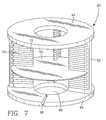
- FIG. 7is an orthographic view of another silicon tower usable with a high-temperature reflow process.
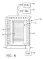
- FIG. 8is a schematic orthographic view of a tubular reactor having silicon sidewalls.
- FIG. 9is a cross-sectional view illustrating the fabrication of a silicon tube by fixing together a plurality of horizontally extending silicon staves.
- FIG. 10is a cross-sectional view of staves having a tongue-and-groove structure.
- FIG. 11is a cross-sectional view of a circularized silicon tube.
- Silicon fixturesparticularly horizontally extending boats, have been frequently suggested and occasionally used in the past. However, their assembly has presented sufficient problems to prevent the widespread use of silicon towers. Many of these problems with silicon support fixtures have been addressed in a set of patents, U.S. Pat. Nos. 6,196,211, 6,205,993, and 6,225,594 to various of Zehavi, Davis, and Delaney. Boyle et al. in U.S. patent application, Ser. No. 09/608,557, filed Jun. 30, 2000, now issued as U.S. Pat. No. 6,450,346, and incorporated herein by reference in its entirety, disclose in detail a method of fabricating one embodiment of such a silicon tower 10 , illustrated in FIG. 2 .
- the tower 10includes multiple silicon legs 12 joined at opposed ends to silicon bases 14 . Teeth 16 are cut into the legs 12 to support the wafers.
- At least the legs 12are composed of virginpolysilicon (virgin poly) formed from the chemical vapor deposition of silane or chlorosilane. Such a material is virtually free of contaminants, particularly the rapidly diffusing metals so deleterious to silicon integrated circuits.
- the basesmay be formed of Czochralski (CZ) silicon, preferably polysilicon although monocrystalline may be used, since virgin poly is not typically available in such large diameters. Other forms of silicon such as cast silicon may be used.
- CZCzochralski
- the processincludes joining the legs 12 to the bases 14 with a spin-on glass (SOG) or other glass-like compound followed by high-temperature ambient annealing at preferably between 1025 and 1400° C. to vitrify the SOG and bond it to the already oxidized silicon parts.
- SOGspin-on glass
- the piecesmay be laser welded together in a process described by Zehavi et al. in U.S. Pat. No. 6,284,997, scheduled to issue on Sep. 4, 2001 and incorporated herein by reference in its entirety.
- the advantage of either methodis forming a continuous planar bond extending along the plane of the interface between the two fixed pieces, unlike the mechanical wedges and surface layer of Niemirowski et al.
- the tower 10After assembly, the tower 10 , including both the legs 12 and bases 14 , is subjected to a surface treatment to introduce controlled sub-surface damage in the silicon.
- a surface treatmentvirtually eliminates the particle problem usually associated with thermal CVD of silicon nitride.
- the surface treatmentnot only removes the thick oxide layer formed in the SOG anneal, but also, as illustrated in the cross-sectional view of FIG. 2 produces pits 20 and cracks 22 penetrating into the treated surface 24 of the silicon part 26 of the tower 10 .
- the silicon part 26may be one of the legs 12 or one of the bases 14 .
- the tower enters serviceit is preferably first subjected to a pre-treatment similar to a typical nitride CVD deposition in which a silicon nitride pre-coat layer 28 not only covers the part surface 24 but also fills the pits 20 and cracks 22 to produce a smooth pre-coat surface 30 .
- Typical thicknesses of the pre-coat layer 28range between 0.1 and 10 ⁇ m.
- no wafersare inserted in the tower slots to be used in production.
- the silicon nitride in the pits 20 and cracks 22firmly anchors the pre-coat layer 28 to the silicon part.
- subsequently deposited silicon nitride layers 32are sequentially deposited over the silicon nitride pre-coat layer 28 , which is firmly anchored to the silicon part 26 .
- differential thermal expansioncontinues to exist between the nitride layers 32 and the underlying bulk silicon 26 , the force exerted at the interface is insufficient to peel the nitride layers 32 from the part 26 .
- An effective method of work treating the silicon surfaceis to roughen it by bead blasting, which is similar to industrial sand blasting.
- a preferred such methodis to blast the surface with particles of silicon carbide of 220 grey grit in a Model 48/PP dry blaster available from Trinity Tool Co. of Fraser, Mich. Particle velocity is controlled by an exit pressure of between about 20 and 80 psi.
- the blasting wandis manually swept over all exposed surfaces of the assembled tower. The blasting need not visibly roughen the silicon surface.
- the silicon surface following the preceding high-temperature SOG annealhas a bluish color, arising from the thick surface oxidation.
- the blastingis continued until the bluish color turns gray, indicative of silicon with perhaps a very thin native oxide.
- the silicon carbide particlesare relatively pure to above 99 %, particularly with respect to metals. Use of particles with significant metal contaminants will likely introduce the metal into the silicon part, rendering the treated part much less useful for processing silicon integrated circuits.
- the treated silicon surfaceis cleaned by vigorous washing with a biodegradable, non-phosphate detergent such as Escolex to remove silicon particles clinging to the surface.
- the final surface roughnesshas been measured to be typically about 32 microinches (0.8 ⁇ m) on the virgin poly legs and 50 microinches (1.3 ⁇ m) on the CZ bases.
- a preferred range of surface roughness, particularly for the legsis 10 to 100 microinches Ra (0.25 to 2.5 ⁇ m Ra).
- a more preferred rangeis 20-75 microinches Ra (0.5-1.9 ⁇ m Ra), and a most preferred range is 30-50 microinches Ra (0.75-1.25 ⁇ m Ra).
- Post-treatment polishingis also not preferred, except possibly in the wafer bearing surfaces which, in a preferred embodiment, are cut into teeth slanting upwards from the legs at 1 to 3° from the horizontal.
- Other hard particlesmay be used for the blasting, such as ceramics.
- the materialmust be substantially free of metals known to readily diffuse in silicon and affect its semiconductor qualities.
- Other types of surface treatmentare possible, such as lapping and grinding. However, these processes are dirty, and offer no apparent advantage.
- the silicon tower 10 fabricated according to the above processis used in a batch CVD reactor 40 , as illustrated in FIG. 6 , which is heated by a resistive coil 42 .
- the reactoris supplied with precursor gases including silane or a chlorosilane such as SiClH 3 and ammonia (NH 3 ) from source 44 , 46 , and a vacuum (exhaust) pump 48 evacuates reactants from the interior of the reactor 40 .
- the pump 48may maintain the interior of the reactor 40 at anywhere in the range from approximately atmospheric pressure for atmospheric pressure CVD (APCDV) down to about 10 Torr for low pressure CVD (LPCVD).
- APCDVatmospheric pressure CVD
- LPCVDlow pressure CVD
- the thermal CVD reactoris typically in the form of a horizontally extending tube, into which the boat bearing multiple wafers is horizontally inserted.
- the same production reactormay be used to pre-coat the silicon nitride layer onto the tower while no wafers are supported in production slots.
- Nitride pre-coatsare believed to provide increased surface integrity of the silicon parts in a hot or harsh environment because of the known toughness of silicon nitride.
- Such surface-treated silicon towerscan be used for hundreds to thousands of runs.
- the nitride build upseems to be limited only by the accumulating nitride filling the slots between the teeth and impeding mechanical clearance of the wafers.
- Such thicknesses of silicon nitridecan be removed by reslotting the teeth or by a long etch in hot hydrofluoric acid.
- Polysiliconis also frequently deposited by thermal CVD typically using a silane or chlorosilane precursor gas.
- a silicon tower for polysilicon CVD depositionis advantageous since the CVD polysilicon is well matched to the virgin poly and possibly other forms of silicon in the tower.
- a smooth silicon tower surfacemay suffice for polysilicon deposition.
- CVD polysilicon flakes from IC wafersAccordingly, if the same mechanism applies to silicon towers, the surface treatment of the invention is useful in providing additional bonding between the bulk silicon parts and the deposited polysilicon layers.
- the silicon tower subjected to the nitride pre-coating described abovecan be used in a very high temperature anneal step, such as a reflow of a silicate glass.
- Thick layers of silicate glassesmay be formed by flame hydrolysis deposition (FHD) in which silane is supplied to a hydrogen and oxygen torch and the flame is passed over the substrate, typically a silicon wafer, to deposit a silicate glass having a nominal composition of SiO 2 .
- Germane or other germanium precursorsmay be additionally included in the flame feed, as well as is water vapor, to affect the refractive index and dielectric constant of the deposited glass.
- the so deposited materialis typically not homogeneous and requires for a commercially popular formulation of the silicate glass a high-temperature reflow at 1350° C. ⁇ 30° C., preferably 1360° C. ⁇ 10 ° C. typically in an air ambient, to convert the material to a homogeneous glass.
- a silicon toweris sufficient for supporting substrates in such a high-temperature process since it remains relatively strong close to its melting point of 1416° C.
- the tower 60has three silicon legs 62 , preferably of virgin polysilicon, joined to two silicon bases 64 with a radial expansion slot 66 formed in the lower one between its outer periphery and an inner aperture 68 .
- Each leg 62includes multiple teeth 70 upwardly inclined at angles of between 86° and 89° with respect to the longitudinal axis of the leg 62 with a support surface 72 formed substantially perpendicularly to the longitudinal axis for supporting one of multiple wafers 50 .
- the support surfaces 72may be polished to a mirror smoothness.
- the legs 62be located at about 120° angular spacings with long teeth 70 having their support surfaces 72 located at about 0.707 of the wafer radius although a position at between 69% and 72% of the wafer radius would provide nearly equal results. Droop can be further reduced by the use of four legs with their support surfaces arranged in a square pattern at 0.707 of the wafer radius.
- the silicate glasstends to drip over the edge of the wafer and to contact the support tower around the edges of the wafer. If the contacted material is silicon, the very hot silicate glass is likely to chemically bond to the silicon. After completion of the reflow when the temperature is reduced, the wafer is believed to be bonded through the reflowed glass to the tower. Excessive force in breaking the bond may chip the silicon of the tower or fracture the wafer, either creating major contamination problems.
- the chipping and fracturingcan be greatly reduced if the assembled silicon tower before use is pre-coated with of a layer of silicon nitride to a thickness in the range of 0.1 to 10 ⁇ m, 0.3 ⁇ m being a typical minimum thickness.
- the deposition onto all areas of the tower used to support production wafermay be performed by chemical vapor deposition, as described above. Nitride tends not to wet other materials such as silica and silicate glasses and the nitride does not react with silica so that the reflowed glass contacting the nitride pre-coat is easily released and removed from the processing chamber with the wafer.
- Wafers annealed on such a nitride pre-coated towerhave been observed to less readily stick to the tower and to not be chipped.
- the silicon towerbe surface treated prior to the nitride pre-coating, in this application, nitride flaking is much less of a problem so that the surface roughening provided by surface treatment may not be needed.
- the surface roughness produced by the surface treatmentincreases the adhesion of the nitride pre-coat layer to the silicon tower and thus further prevents peeling of nitride when the reflowed glass is forcefully removed. Thereby, the integrity of the nitride pre-coat layer is preserved over a long commercial use.
- the same preventive mechanismis useful when the wafer is being flame hydrolyzed while supported on a silicon pedestal fixture pre-coated with a nitride layer.
- a tubular sleeve 76may be inserted in the CVD reactor 40 of FIG. 6 to control the flow of gases in the reactor. Whatever deposition occurs also coats the interior of the sleeve 76 , which may be removed and replaced.
- the sleeve 76has been composed of quartz. A quartz sleeve suffers many of the same problems as a quartz tower. Instead, according to the invention, the sleeve 76 is composed of silicon having a tubularly shaped wall of about 2 to 5 mm thickness.
- At least its interior wallsare surface treated by bead blasting or the like to provide a good anchor for the deposition of many layers of silicon nitride.
- the lifetime of the treated silicon sleeve 76is substantially longer than that of a quartz sleeve.
- a silicon chamber part shaped similarly to the silicon sleeve 76is a silicon reactor tube 80 illustrated in the schematic orthographic view of FIG. 8 . It has a circularly symmetric wall 82 of thickness t enclosing a bore 84 of diameter D.
- a resistive heater 86is wrapped around the tube 80 and is powered by a power supply 88 to heat the interior of the reactor to elevated temperatures. Other forms of heating are possible, such as radiant or RF inductive heating. If the silicon tube 80 has sufficiently high doping so as to be highly conductive, the RF energy may be coupled directly into the tube 80 , in which case the power supply 88 supplies RF power rather than AC or DC and the wire 86 may be offset from the tube wall 82 .
- the diameter Dis large enough to accommodate a wafer tower or wafer boat supporting a number of wafers. That is, the diameter D is somewhat larger than the wafer diameter of, for example, 200 or 300 mm.
- the tubeis arranged vertically, for a boat, the tube is arranged horizontally and preferably the boat is support on rails cantilevered parallel to the tube wall 82 . In either case, the support fixture loaded with wafers is placed in the reactor tube. In a vertically arranged reactor, either the tube is lowered over a stationary tower or the tower may be inserted vertically into a stationary tube. On the other hand, a wafer boat is moved horizontally into a stationary horizontally arranged reactor tube.
- the silicon tube 80is held between unillustrated end caps, preferably formed of surface-treated silicon, providing a support for the tower or boat and ports for the supply gases and exhaust or vacuum pump of FIG. 6 . If necessary, the end caps are vacuum sealed to the tube 80 for the relatively modest vacuums required.
- the thickness of the tube wall 82is preferably at least 3 mm and more preferably at least 5 mm. Such a reactor tube thereby allows a large portion of the exposed surfaces of the reactor to be composed of high-purity silicon.
- Such reactor tubesare used for thermal CVD of silicon nitride and polysilicon, as previously described, for wet or dry thermal oxidation of silicon, for diffusion doping from an ambient including the doping material, inert annealing including a dopant drive-in, and for other high temperature processes.
- the interior surface of the tube wall 84is surface treated to provide additional adhesion to the deposition material.
- pedestals, pedestal rings, and railstypically formed of quartz in the past, may instead be formed of silicon, preferably virgin poly if it is available in adequate sizes, and thereafter surface treated as described above.
- virgin polyis particularly advantageous for silicon parts which contact the wafer
- other chamber partssuch as the above described sleeve and wall do not require the very high purity levels associated with virgin poly.
- the surface treatment described abovemay be applied to other forms of silicon, for example, float zone (FZ) silicon, CZ silicon, cast silicon, edge film grown (EFG) silicon, the last two forms of which are prevalently used for solar cells, or other types such as extruded silicon. It is also possible to perform the described surface treatment on a silicon film deposited on another base material, for example, by CVD.
- virgin polysiliconis not available in diameters greater than 200 mm required for the sleeve and reactor tube described above. Silicon of lesser purity is acceptable in many processing applications in which a high-temperature silicon part does not touch the silicon wafer. Nonetheless, the silicon parts should be made of silicon that is substantially pure, for example, has a impurity atomic fraction of metals of less than one part per million and of other components including oxygen, nitrogen, and carbon of substantially less than 1% and preferably less than 50 parts per million. Alternatively, the silicon may be characterized as being semiconductive.
- One method of forming the tubular silicon sleeve and wall described aboveis extrusion of silicon in a circularly symmetric tubular shape in a process also called edge film growth (EFG).
- EFGedge film growth
- Some older technology for doctor-blade extrusion of siliconis disclosed by Grabmaier et al. in U.S. Pat. Nos. 4,330,358 and 4,357,201. This technology sinters the extruded form and uses germanium sintering aids, including semiconductor dopants if desired.
- More recent technology including extruding silicon tubesis disclosed by Stormont et al. in U.S. Pat. No. 4,440,728 and by Harvey et al. in U.S. Pat. No. 5,102,494. GT Equipment Technologies, Inc.
- Silicon chamber wallsmay alternatively be formed by bonding together a relatively small number of silicon plates in a closed pattern as one would assemble staves into a barrel.
- this techniqueis not always successful because the polygonal shape may introduce non-uniform flow patterns.
- the bonding agent used to fix the plates togethermay be a contaminant for semiconductor processing.
- a large number of staves 90are machined to have a cross-sectional shape of symmetric trapezoids with two parallel faces 92 , 94 and two faces 96 inclined with respect to each other at angles so that the faces 96 of neighboring staves 90 are parallel.
- the shapeuniformly extends along an axial direction.
- the staves 90are composed of silicon, preferably virgin polysilicon The machining of virgin polysilicon is described in the afore cited U.S. patent application Ser. No. 09/608,557.
- the staves 90number at least twelve and preferably twenty or more. Other shapes are possible, but the symmetric trapezoid is preferred to ease machining and assembly.
- the staves 90are assembled in a closed pattern with their longitudinal axes oriented parallel to a central axis 98 with the inclined sides 96 of neighboring staves 90 abutting each other to form a tightly fitting polygonal tube 100 formed in a generally circular pattern about the central axis 98 .
- the large number of stavesreduces the interior asymmetry of the assembled tube and simplifies any circularizing.
- the staves 90can be held together prior to being bonded together by sleeves or hoops of quartz or other material placed around their ends.
- the staves 90are then fixed together to form a wall.
- the silicon tubeneed not be vacuum tight. However, for a silicon vacuum wall, the joints must be made vacuum tight.
- the fixing processmay include applying a thinned spin-on silica glass (SOG) to the inclined faces 96 before assembling the staves 90 and thereafter curing the spin-on glass, as described in previously cited U.S. patent application Ser. No. 09/608,557. While this method is effective for tubes used at lower processing temperatures, the method suffers at very high processing temperatures because the silica glass softens at elevated temperatures. Instead, it is preferred to use a silicon welding technique described by Zehavi et al. in U.S. Pat. No. 6,284,997. For a non-vacuum wall, the staves 90 may be spot welded at their ends or at occasional spots along their length, and the clean silicon weld described in U.S. Pat. No. 6,284,997 is not required. For a vacuum wall, however, a full welding bead needs to extend along at least one side of the interface between the inclined faces 96 of the staves 90 , and the weld must be smooth and clean.
- SOG
- staves 90The joining of the staves 90 is simplified if staves 102 , illustrated in cross-sectional view of FIG. 10 are machined into generally trapezoidal form but with respective axially extending tongues 104 and grooves 106 are formed in the opposing inclined faces 96 .
- the staves 102are then assembled by fitting the tongue of one stave 102 into the groove 106 of the neighboring stave 102 with the neighboring inclined faces 106 in abutment. If multiple tongues and grooves are used, the resulting structure has a corrugated joint.
- the tubemay be desired to form the tube to have a circularized inner surface.
- the joined polygonal tube 100is machined on its inside, for example on a lathe or reamer, to form a cylindrical inner surface 108 symmetric about the central axis 98 .
- the resulting tube 110has a circular inner wall 100 and a polygonal outer wall.
- the interior circular shapegreatly simplifies gas flow dynamics during processing of wafers.
- the outer wallmay also be circularized, but this further step is not always necessary.
- the tube 100 or 102may then be stress annealed or have its inner surface bead blasted or otherwise processed to introduce sub-surface damage. Pre-coats of the sort previously described may also be applied.
- the silicon parts of the inventionare not limited to batch mode thermal CVD reactors. They can be used for plasma CVD and other low temperature processes performed with wafer temperatures below 400° C.
- a single-wafer plasma CVD reactorhas a side wall and a dome onto which the intended deposition material is likely to also be deposited.
- the wall and domehave been typically made of quartz, and a plasma cleaning process has been used to clean the wall and dome surfaces, either between every wafer run or on a less frequent schedule. If the quartz wall, dome, or other part is replaced with a corresponding silicon part surface treated as described above, the plasma cleaning may be eliminated or perhaps delayed until a planned maintenance shutdown.
- Plasma etching reactorsare also subject to deposition of polymeric material and other residues on the chamber walls and parts. The roughened silicon described above will more firmly anchor the residues and reduce the production of particulates.
- the inventionthus provides a generic approach for reducing particles in substrate processing reactors by the use of surface worked silicon parts. Nonetheless, the silicon material of the parts is readily available at reasonable costs and does not require complex processing.
Landscapes
- Chemical & Material Sciences (AREA)
- Engineering & Computer Science (AREA)
- Materials Engineering (AREA)
- Metallurgy (AREA)
- Organic Chemistry (AREA)
- Chemical Kinetics & Catalysis (AREA)
- General Chemical & Material Sciences (AREA)
- Crystallography & Structural Chemistry (AREA)
- Mechanical Engineering (AREA)
- Physics & Mathematics (AREA)
- Thermal Sciences (AREA)
- Condensed Matter Physics & Semiconductors (AREA)
- General Physics & Mathematics (AREA)
- Manufacturing & Machinery (AREA)
- Computer Hardware Design (AREA)
- Microelectronics & Electronic Packaging (AREA)
- Power Engineering (AREA)
- Chemical Vapour Deposition (AREA)
- Silicon Compounds (AREA)
Abstract
Description
- This application is a division of Ser. No. 10/642,013, filed Aug. 15, 2003, which is a division of Ser. No. 09/965,106, filed Sep. 26, 2001, which is a continuation in part of Ser. No. 09/860,392, filed May 18, 2001 and to be issued on Sep. 19, 2006 as U.S. Pat. No. 7,108,746.
- 1. Field of the Invention
- The invention relates generally to silicon structures. In particular the invention relates to silicon tubes useful in reactors used in batch-mode semiconductor processing such as chemical vapor deposition and high temperature annealing.
- 2. Background Art
- The fabrication of silicon integrated circuits typically involves one or more steps of chemical vapor deposition (CVD). Many advanced deposition processes use plasma enhanced CVD to activate the chemical reaction resulting in the deposition of the film from a precursor gas. The plasma process allows low temperature deposition. On the other hand, thermal CVD is performed at elevated temperatures to thermally activate the chemical reaction resulting in the deposition of the film from a precursor gas. The temperatures associated with thermal CVD tend to be much higher than those for plasma enhanced CVD, but thermal CVD temperatures fall within a wide range depending upon the material being deposited and the precursor gas.
- Thermal CVD is typically utilized for the deposition of silicon nitride and polysilicon. The silicon nitride is used, for example, for etch stop layers and anti-reflective coatings. Silicon nitride has a nominal composition of Si3N4, but some compositional variation is expected, such as SiNx, where x ranges between 1.0 and 1.5. Polysilicon is polycrystalline silicon. It is used for anti-reflective coating and, when doped, for interconnects and electrodes.
- Despite the trend to single-wafer processing chambers, batch processing for thermal CVD continues to be widely practiced because of its high throughput and the relatively low cost of equipment. Furthermore, thermal CVD can produce highly uniform films in batch processing. In batch CVD processing, a large number of silicon wafers are loaded onto a support fixture that is placed into a thermal CVD reactor. Typically, the support fixture is a tower in which the multiple wafers are supported horizontally and spaced vertically apart. Some applications continue to use boats as support fixture in which the multiple wafers are supported substantially vertically and spaced horizontally apart.
- In the case of the deposition of silicon nitride, the precursor gas is typically composed of a silane or a chlorosilane and a nitrogen source such ammonia. At elevated temperatures, typically in the range of 600 to 800° C. but sometimes extending down to 400° C. or even lower, the precursors react near the surface of the wafer to deposit silicon nitride on the wafer surface. In the case of chlorosilane and ammonia precursors, the reaction products are Si3N4and NH4Cl. The former deposits on the wafer while the latter is volatile and is evacuated from the furnace. However, thermal CVD tends to coat all surfaces exposed in the furnace. In particular, the support tower is typically coated with as much silicon nitride as is the wafer. Further, the walls of the reactor, typically formed in a tubular shape, also tend to be coated.
- Quartz has in the past been the most prevalently used material for support towers and tubes used in a thermal CVD process and other high-temperature processes. Quartz has a chemical composition of amorphous silicon dioxide, which is compatible with most silicon processing. At the relatively low temperatures usually experienced in CVD, whether thermal or plasma enhanced, quartz remains in a glassy state with a very smooth surface so that it is a very clean material. However, as the feature sizes on integrated circuits has decreased to 0.18 μm and even smaller, quartz support towers have nonetheless experienced substantial problems because of their tendency to produce particles. These particulates fall on the wafer and can significantly reduce the yield of operable integrated circuit dies obtained from the wafer.
- Often integrated circuit fabrication is monitored by measuring the number of particles added to a wafer by any step of the fabrication process. It has been found in thermal CVD of silicon nitride that the number of particles generally increases with the number of runs or batches that the quartz tower has processed. As illustrated in
FIG. 1 , a new tower produces relatively few particles. Thereafter, the number of particles increases with the number of runs, but up to about forty runs the number is acceptable, though still somewhat high. However, after some number of runs, the number of particles greatly increases to a totally unacceptable level. It is believed that the origin of the problem is that the silicon nitride is also depositing on the quartz tower. For 40 runs of depositing 0.15 μm of silicon nitride, a typical nitride layer thickness in an integrated circuit, the nitride may build up on the tower to a thickness of 6 μm. Silicon nitride has a coefficient of thermal expansion that is significantly different than that of quartz, about 3×10⁻⁶versus 0.5×10⁻⁶/° C., and the nitride does not bond well with the glassy quartz surface. Differential thermal expansion between the two materials as the tower is cycled between room temperature and the relatively modest thermal CVD temperatures causes the thickly deposited nitride to peel from the quartz and to produce nitride particles, some of which settle on the wafers. - For these reasons, it is typical practice in a production environment to use a tower only for a predetermined number of runs somewhat below the experimentally determined point at which the particle count rapidly increases, for example, thirty runs for the data displayed in
FIG. 1 . It is common practice to then clean the quartz tower in bath of hydrofluoric acid and nitric acid to remove the silicon nitride and to return the cleaned tower to service for another cycle of runs. However, the baseline particle count for a cleaned tower is somewhat higher than that for a new tower, and the number of runs before onset of unacceptable particle count is reduced by about 25%. As a result, quartz towers are typically discarded after only two or three cycles. Although quartz towers are relatively inexpensive, such short life greatly increases the cost of ownership (COO) when measured per wafer. Also, the necessity of changing out towers and cleaning towers complicates the work flow and reduces productivity. - Furthermore, the baseline particle counts for quartz towers are still high, and the onset of greatly increased counts is somewhat variable. Both factors reduce the yield of operable dice obtained from the wafers.
- Quartz tubes are also often replaced after a finite number of batches although the problem being addressed is often fracturing of the quartz tube.
- Some of these reasons have prompted the use of silicon carbide towers. Bulk silicon carbide is typically formed by a sintering process, which produces a material containing a high fraction of impurities. For this reason, the sintered material is usually covered with a layer of CVD silicon carbide. As long as the CVD layer is not punctured, contamination is not a problem. The peeling problem is not totally eliminated. However, after a nitride buildup of about 20 μm on the silicon carbide tower, it can cleaned in a mixed acid etch for up to a week with the result that the tower can be used almost indefinitely. However, the CVD silicon carbide film is fragile, and a single pin hole through the film ruins the protective coating resulting in the necessity that the tower be scrapped. Entire towers of CVD silicon carbide can be made, but they are very expensive.
- Accordingly, it is greatly desired to provide a support tower that is not subject to such particle problems and can be used for many more runs without cleaning or replacement.
- Suggestions have been made to form wafer support towers from silicon, particularly polysilicon. See, for example, U.S. Pat. No. 6,056,123 to Niemirowski et al. They fabricate their towers from silicon legs mechanically wedged into silicon end plates, and a layer of polysilicon is then deposited by chemical vapor deposition on the assembled structure to provide additional strength. Their tower fabrication is believed to still be weak. Further, when silicon towers are used to support wafer preformed with a silica glass that requires reflowing at high temperature, the wafers have been observed to stick to the tower after reflow. Forcefully removing the stuck wafer may result in the tower becoming chipped. Some believe that the silica glass reflows over the edge of the wafer and intimately bonds with the exposed silicon and a silica bridge is formed between the wafer and the tower.
- The invention includes a method of chemical vapor deposition (CVD), particularly thermal CVD, and more particularly deposition of silicon nitride, polysilicon, and related materials, onto multiple wafers supported on a silicon fixture, for example, a tower. Preferably, the silicon fixture is composed of virgin polysilicon. Also, preferably, surfaces of the silicon tower are subjected to surface treatment, such as bead blasting by hard particles, for example, of silicon carbide. The surface treatment may be characterized as introducing sub-surface damage in the silicon part.
- The invention also includes such a silicon fixture and its fabrication method. The surface of the fixture has a roughness preferably in the range of 10-100 microinches Ra (0.25-2.5 μm), more preferably 20-75 microinches Ra (0.5-1.9 μm), and most preferably 35-50 microinches Ra (0.9-1.25 μm).
- The invention further includes other surface treated silicon parts usable in a CVD reactor or other high-temperature substrate processing reactor.
- According to another aspect of the invention, a silicon tower is pre-coated with a thin layer, for example, by chemical vapor deposition. When the tower is supporting wafers in high-temperature deposition of silicon nitride or polysilicon, the tower is preferably initially pre-coated with a thin layer of silicon nitride or polysilicon respectively. Cracks and pits produced the surface treatment firmly anchors the initial film and subsequently deposited films. When the tower is supporting wafers in high-temperature deposition or oxidation producing silica, the tower is preferably initially coated with a thin layer of silicon nitride.
- The invention is further applicable to a high-temperature reflow step following deposition of silica layer, for example, by CVD or flame hydrolysis. The reflow step is typically performs at above 1200° C., preferably at 1350±30° C. for a commonly used silica formulation, and most preferably at 1360±10° C.
- In a further aspect of the invention, silicon tubular members may advantageously be used for liners in CVD reactors and for tubular reactor walls used in high-temperature processing. Such silicon tubular members may conveniently be formed by extrusion, whether or not the tube is surface treated, or by bonding together in a polygonal shape a large number of trapezoidally shaped staves and preferably thereafter machining the interior to form a cylindrical bore. Such silicon tubes are often advantageously surface treated and pre-coated.
FIG. 1 is a schematic chart showing the generation of particles during batch thermal chemical vapor deposition using a quartz tower of the prior art.FIG. 2 is an orthographic view of a silicon tower fabricated according to the invention and usable in the processes of the invention.FIG. 3 is a cross -sectional view of a surface of the silicon tower after bead blasting.FIG. 4 is a cross-sectional view of the silicon tower surface ofFIG. 3 after deposition of a pre-coat layer.FIG. 5 is a cross-sectional view of the silicon tower surface ofFIG. 4 after many runs of depositing silicon nitride.FIG. 6 is a schematic cross-sectional view of a thermal CVD reactor in which a process of the invention may be practiced and in which the tower or shield of the invention may be used.FIG. 7 is an orthographic view of another silicon tower usable with a high-temperature reflow process.FIG. 8 is a schematic orthographic view of a tubular reactor having silicon sidewalls.FIG. 9 is a cross-sectional view illustrating the fabrication of a silicon tube by fixing together a plurality of horizontally extending silicon staves.FIG. 10 is a cross-sectional view of staves having a tongue-and-groove structure.FIG. 11 is a cross-sectional view of a circularized silicon tube.- Silicon fixtures, particularly horizontally extending boats, have been frequently suggested and occasionally used in the past. However, their assembly has presented sufficient problems to prevent the widespread use of silicon towers. Many of these problems with silicon support fixtures have been addressed in a set of patents, U.S. Pat. Nos. 6,196,211, 6,205,993, and 6,225,594 to various of Zehavi, Davis, and Delaney. Boyle et al. in U.S. patent application, Ser. No. 09/608,557, filed Jun. 30, 2000, now issued as U.S. Pat. No. 6,450,346, and incorporated herein by reference in its entirety, disclose in detail a method of fabricating one embodiment of such a
silicon tower 10, illustrated inFIG. 2 . Thetower 10 includesmultiple silicon legs 12 joined at opposed ends to silicon bases14.Teeth 16 are cut into thelegs 12 to support the wafers. - It is preferred that at least the
legs 12 are composed of virginpolysilicon (virgin poly) formed from the chemical vapor deposition of silane or chlorosilane. Such a material is virtually free of contaminants, particularly the rapidly diffusing metals so deleterious to silicon integrated circuits. The bases may be formed of Czochralski (CZ) silicon, preferably polysilicon although monocrystalline may be used, since virgin poly is not typically available in such large diameters. Other forms of silicon such as cast silicon may be used. The process includes joining thelegs 12 to thebases 14 with a spin-on glass (SOG) or other glass-like compound followed by high-temperature ambient annealing at preferably between 1025 and 1400° C. to vitrify the SOG and bond it to the already oxidized silicon parts. Alternatively, the pieces may be laser welded together in a process described by Zehavi et al. in U.S. Pat. No. 6,284,997, scheduled to issue on Sep. 4, 2001 and incorporated herein by reference in its entirety. The advantage of either method is forming a continuous planar bond extending along the plane of the interface between the two fixed pieces, unlike the mechanical wedges and surface layer of Niemirowski et al. - After assembly, the
tower 10, including both thelegs 12 andbases 14, is subjected to a surface treatment to introduce controlled sub-surface damage in the silicon. Such a surface treatment virtually eliminates the particle problem usually associated with thermal CVD of silicon nitride. We believe that the surface treatment not only removes the thick oxide layer formed in the SOG anneal, but also, as illustrated in the cross-sectional view ofFIG. 2 producespits 20 andcracks 22 penetrating into the treatedsurface 24 of thesilicon part 26 of thetower 10. Thesilicon part 26 may be one of thelegs 12 or one of thebases 14. - When the tower enters service, it is preferably first subjected to a pre-treatment similar to a typical nitride CVD deposition in which a silicon
nitride pre-coat layer 28 not only covers thepart surface 24 but also fills thepits 20 andcracks 22 to produce a smoothpre-coat surface 30. Typical thicknesses of thepre-coat layer 28 range between 0.1 and 10 μm. Preferably, during the pre-treatment, no wafers are inserted in the tower slots to be used in production. The silicon nitride in thepits 20 andcracks 22 firmly anchors thepre-coat layer 28 to the silicon part. Thereafter, when the tower enters normal production, subsequently deposited silicon nitride layers32 are sequentially deposited over the siliconnitride pre-coat layer 28, which is firmly anchored to thesilicon part 26. Although differential thermal expansion continues to exist between the nitride layers32 and theunderlying bulk silicon 26, the force exerted at the interface is insufficient to peel the nitride layers32 from thepart 26. - An effective method of work treating the silicon surface is to roughen it by bead blasting, which is similar to industrial sand blasting. A preferred such method is to blast the surface with particles of silicon carbide of 220 grey grit in a
Model 48/PP dry blaster available from Trinity Tool Co. of Fraser, Mich. Particle velocity is controlled by an exit pressure of between about 20 and 80 psi. In the bead blasting, the blasting wand is manually swept over all exposed surfaces of the assembled tower. The blasting need not visibly roughen the silicon surface. The silicon surface following the preceding high-temperature SOG anneal has a bluish color, arising from the thick surface oxidation. The blasting is continued until the bluish color turns gray, indicative of silicon with perhaps a very thin native oxide. Preferably, the silicon carbide particles are relatively pure to above99%, particularly with respect to metals. Use of particles with significant metal contaminants will likely introduce the metal into the silicon part, rendering the treated part much less useful for processing silicon integrated circuits. - Following bead blasting, the treated silicon surface is cleaned by vigorous washing with a biodegradable, non-phosphate detergent such as Escolex to remove silicon particles clinging to the surface. A final clean with a high-pressure carbon dioxide gun, such as Sno Blo, removes any remaining particles. The final surface roughness has been measured to be typically about 32 microinches (0.8 μm) on the virgin poly legs and 50 microinches (1.3 μm) on the CZ bases. A preferred range of surface roughness, particularly for the legs, is 10 to 100 microinches Ra (0.25 to 2.5 μm Ra). A more preferred range is 20-75 microinches Ra (0.5-1.9 μm Ra), and a most preferred range is 30-50 microinches Ra (0.75-1.25 μm Ra).
- It is preferred that no post-treatment etching be performed as this would likely remove the pits and cracks. Post-treatment polishing is also not preferred, except possibly in the wafer bearing surfaces which, in a preferred embodiment, are cut into teeth slanting upwards from the legs at 1 to 3° from the horizontal.
- Other hard particles may be used for the blasting, such as ceramics. However, the material must be substantially free of metals known to readily diffuse in silicon and affect its semiconductor qualities. Other types of surface treatment are possible, such as lapping and grinding. However, these processes are dirty, and offer no apparent advantage.
- The
silicon tower 10 fabricated according to the above process is used in abatch CVD reactor 40, as illustrated inFIG. 6 , which is heated by aresistive coil 42. The reactor is supplied with precursor gases including silane or a chlorosilane such as SiClH3and ammonia (NH3) fromsource reactor 40. Thepump 48 may maintain the interior of thereactor 40 at anywhere in the range from approximately atmospheric pressure for atmospheric pressure CVD (APCDV) down to about 10 Torr for low pressure CVD (LPCVD).Multiple wafers 50 are loaded into thetower 10 and processed as described above to deposit the silicon nitride in one batch run. When a boat instead of a tower is used, the thermal CVD reactor is typically in the form of a horizontally extending tube, into which the boat bearing multiple wafers is horizontally inserted. The same production reactor may be used to pre-coat the silicon nitride layer onto the tower while no wafers are supported in production slots. - Nitride pre-coats are believed to provide increased surface integrity of the silicon parts in a hot or harsh environment because of the known toughness of silicon nitride.
- Such surface-treated silicon towers can be used for hundreds to thousands of runs. The nitride build up seems to be limited only by the accumulating nitride filling the slots between the teeth and impeding mechanical clearance of the wafers. Such thicknesses of silicon nitride can be removed by reslotting the teeth or by a long etch in hot hydrofluoric acid.
- Polysilicon is also frequently deposited by thermal CVD typically using a silane or chlorosilane precursor gas. A silicon tower for polysilicon CVD deposition is advantageous since the CVD polysilicon is well matched to the virgin poly and possibly other forms of silicon in the tower. A smooth silicon tower surface may suffice for polysilicon deposition. However, it has been observed that CVD polysilicon flakes from IC wafers. Accordingly, if the same mechanism applies to silicon towers, the surface treatment of the invention is useful in providing additional bonding between the bulk silicon parts and the deposited polysilicon layers.
- The silicon tower subjected to the nitride pre-coating described above can be used in a very high temperature anneal step, such as a reflow of a silicate glass. Thick layers of silicate glasses may be formed by flame hydrolysis deposition (FHD) in which silane is supplied to a hydrogen and oxygen torch and the flame is passed over the substrate, typically a silicon wafer, to deposit a silicate glass having a nominal composition of SiO2. Germane or other germanium precursors may be additionally included in the flame feed, as well as is water vapor, to affect the refractive index and dielectric constant of the deposited glass. However, the so deposited material is typically not homogeneous and requires for a commercially popular formulation of the silicate glass a high-temperature reflow at 1350° C.±30° C., preferably1360° C.±10° C. typically in an air ambient, to convert the material to a homogeneous glass. Some other types of glasses reflow at as low as 600° C., but the problems described below tend to become problems only at reflow annealing temperatures of greater than 1200° C. A silicon tower is sufficient for supporting substrates in such a high-temperature process since it remains relatively strong close to its melting point of 1416° C.
- One
such silicon tower 60, illustrated in the orthographic view ofFIG. 7 , was designed for such a high-temperature process. Thetower 60 has threesilicon legs 62, preferably of virgin polysilicon, joined to twosilicon bases 64 with aradial expansion slot 66 formed in the lower one between its outer periphery and aninner aperture 68. Eachleg 62 includesmultiple teeth 70 upwardly inclined at angles of between 86° and 89° with respect to the longitudinal axis of theleg 62 with asupport surface 72 formed substantially perpendicularly to the longitudinal axis for supporting one ofmultiple wafers 50. The support surfaces72 may be polished to a mirror smoothness. In order to minimize wafer droop at the very high processing temperatures, it is preferred that thelegs 62 be located at about 120° angular spacings withlong teeth 70 having their support surfaces72 located at about 0.707 of the wafer radius although a position at between 69% and 72% of the wafer radius would provide nearly equal results. Droop can be further reduced by the use of four legs with their support surfaces arranged in a square pattern at 0.707 of the wafer radius. - However, at the temperatures required for reflow, the silicate glass tends to drip over the edge of the wafer and to contact the support tower around the edges of the wafer. If the contacted material is silicon, the very hot silicate glass is likely to chemically bond to the silicon. After completion of the reflow when the temperature is reduced, the wafer is believed to be bonded through the reflowed glass to the tower. Excessive force in breaking the bond may chip the silicon of the tower or fracture the wafer, either creating major contamination problems.
- The chipping and fracturing can be greatly reduced if the assembled silicon tower before use is pre-coated with of a layer of silicon nitride to a thickness in the range of 0.1 to 10 μm, 0.3 μm being a typical minimum thickness. The deposition onto all areas of the tower used to support production wafer may be performed by chemical vapor deposition, as described above. Nitride tends not to wet other materials such as silica and silicate glasses and the nitride does not react with silica so that the reflowed glass contacting the nitride pre-coat is easily released and removed from the processing chamber with the wafer. Wafers annealed on such a nitride pre-coated tower have been observed to less readily stick to the tower and to not be chipped. Although it is recommended that the silicon tower be surface treated prior to the nitride pre-coating, in this application, nitride flaking is much less of a problem so that the surface roughening provided by surface treatment may not be needed. However, the surface roughness produced by the surface treatment increases the adhesion of the nitride pre-coat layer to the silicon tower and thus further prevents peeling of nitride when the reflowed glass is forcefully removed. Thereby, the integrity of the nitride pre-coat layer is preserved over a long commercial use.
- The same preventive mechanism is useful when the wafer is being flame hydrolyzed while supported on a silicon pedestal fixture pre-coated with a nitride layer.
- Although the invention is particularly useful for support towers and boats supporting multiple wafers, it may also be applied to other parts that are exposed to deposition. For example, a
tubular sleeve 76 may be inserted in theCVD reactor 40 ofFIG. 6 to control the flow of gases in the reactor. Whatever deposition occurs also coats the interior of thesleeve 76, which may be removed and replaced. In the past, thesleeve 76 has been composed of quartz. A quartz sleeve suffers many of the same problems as a quartz tower. Instead, according to the invention, thesleeve 76 is composed of silicon having a tubularly shaped wall of about 2 to 5 mm thickness. At least its interior walls are surface treated by bead blasting or the like to provide a good anchor for the deposition of many layers of silicon nitride. The lifetime of the treatedsilicon sleeve 76 is substantially longer than that of a quartz sleeve. - A silicon chamber part shaped similarly to the
silicon sleeve 76 is asilicon reactor tube 80 illustrated in the schematic orthographic view ofFIG. 8 . It has a circularlysymmetric wall 82 of thickness t enclosing abore 84 of diameter D. Aresistive heater 86 is wrapped around thetube 80 and is powered by apower supply 88 to heat the interior of the reactor to elevated temperatures. Other forms of heating are possible, such as radiant or RF inductive heating. If thesilicon tube 80 has sufficiently high doping so as to be highly conductive, the RF energy may be coupled directly into thetube 80, in which case thepower supply 88 supplies RF power rather than AC or DC and thewire 86 may be offset from thetube wall 82. - The diameter D is large enough to accommodate a wafer tower or wafer boat supporting a number of wafers. That is, the diameter D is somewhat larger than the wafer diameter of, for example, 200 or 300 mm. For a tower, the tube is arranged vertically, for a boat, the tube is arranged horizontally and preferably the boat is support on rails cantilevered parallel to the
tube wall 82. In either case, the support fixture loaded with wafers is placed in the reactor tube. In a vertically arranged reactor, either the tube is lowered over a stationary tower or the tower may be inserted vertically into a stationary tube. On the other hand, a wafer boat is moved horizontally into a stationary horizontally arranged reactor tube. - The
silicon tube 80 is held between unillustrated end caps, preferably formed of surface-treated silicon, providing a support for the tower or boat and ports for the supply gases and exhaust or vacuum pump ofFIG. 6 . If necessary, the end caps are vacuum sealed to thetube 80 for the relatively modest vacuums required. The thickness of thetube wall 82 is preferably at least 3 mm and more preferably at least 5 mm. Such a reactor tube thereby allows a large portion of the exposed surfaces of the reactor to be composed of high-purity silicon. Such reactor tubes, previously made of quartz or sometimes silicon carbide, are used for thermal CVD of silicon nitride and polysilicon, as previously described, for wet or dry thermal oxidation of silicon, for diffusion doping from an ambient including the doping material, inert annealing including a dopant drive-in, and for other high temperature processes. Advantageously, especially for thermal CVD, the interior surface of thetube wall 84 is surface treated to provide additional adhesion to the deposition material. - Other parts in this or other deposition chambers, such as pedestals, pedestal rings, and rails, typically formed of quartz in the past, may instead be formed of silicon, preferably virgin poly if it is available in adequate sizes, and thereafter surface treated as described above.
- Although virgin poly is particularly advantageous for silicon parts which contact the wafer, other chamber parts such as the above described sleeve and wall do not require the very high purity levels associated with virgin poly. The surface treatment described above may be applied to other forms of silicon, for example, float zone (FZ) silicon, CZ silicon, cast silicon, edge film grown (EFG) silicon, the last two forms of which are prevalently used for solar cells, or other types such as extruded silicon. It is also possible to perform the described surface treatment on a silicon film deposited on another base material, for example, by CVD.
- At the present time, virgin polysilicon is not available in diameters greater than 200 mm required for the sleeve and reactor tube described above. Silicon of lesser purity is acceptable in many processing applications in which a high-temperature silicon part does not touch the silicon wafer. Nonetheless, the silicon parts should be made of silicon that is substantially pure, for example, has a impurity atomic fraction of metals of less than one part per million and of other components including oxygen, nitrogen, and carbon of substantially less than 1% and preferably less than 50 parts per million. Alternatively, the silicon may be characterized as being semiconductive.
- One method of forming the tubular silicon sleeve and wall described above is extrusion of silicon in a circularly symmetric tubular shape in a process also called edge film growth (EFG). Some older technology for doctor-blade extrusion of silicon is disclosed by Grabmaier et al. in U.S. Pat. Nos. 4,330,358 and 4,357,201. This technology sinters the extruded form and uses germanium sintering aids, including semiconductor dopants if desired. More recent technology including extruding silicon tubes is disclosed by Stormont et al. in U.S. Pat. No. 4,440,728 and by Harvey et al. in U.S. Pat. No. 5,102,494. GT Equipment Technologies, Inc. of Nashua, New Hampshire has commercialized and markets technology for extruding large hollow silicon members in polygonal shapes, and sells an extruder under the trade name GIi EFG Puller. It has long been known to form small-diameter sapphire circular and polygonal tubes by EFG.
- Silicon chamber walls may alternatively be formed by bonding together a relatively small number of silicon plates in a closed pattern as one would assemble staves into a barrel. However, this technique is not always successful because the polygonal shape may introduce non-uniform flow patterns. Further, the bonding agent used to fix the plates together may be a contaminant for semiconductor processing.
- An improvement of the stave approach is illustrated in the cross-sectional view of
FIG. 9 . A large number ofstaves 90 are machined to have a cross-sectional shape of symmetric trapezoids with twoparallel faces faces 96 inclined with respect to each other at angles so that thefaces 96 of neighboringstaves 90 are parallel. The shape uniformly extends along an axial direction. Thestaves 90 are composed of silicon, preferably virgin polysilicon The machining of virgin polysilicon is described in the afore cited U.S. patent application Ser. No. 09/608,557. Thestaves 90 number at least twelve and preferably twenty or more. Other shapes are possible, but the symmetric trapezoid is preferred to ease machining and assembly. - The
staves 90 are assembled in a closed pattern with their longitudinal axes oriented parallel to acentral axis 98 with theinclined sides 96 of neighboringstaves 90 abutting each other to form a tightly fittingpolygonal tube 100 formed in a generally circular pattern about thecentral axis 98. The large number of staves reduces the interior asymmetry of the assembled tube and simplifies any circularizing. Thestaves 90 can be held together prior to being bonded together by sleeves or hoops of quartz or other material placed around their ends. Thestaves 90 are then fixed together to form a wall. For a tubular silicon liner used within another tube, the silicon tube need not be vacuum tight. However, for a silicon vacuum wall, the joints must be made vacuum tight. - The fixing process may include applying a thinned spin-on silica glass (SOG) to the inclined faces96 before assembling the
staves 90 and thereafter curing the spin-on glass, as described in previously cited U.S. patent application Ser. No. 09/608,557. While this method is effective for tubes used at lower processing temperatures, the method suffers at very high processing temperatures because the silica glass softens at elevated temperatures. Instead, it is preferred to use a silicon welding technique described by Zehavi et al. in U.S. Pat. No. 6,284,997. For a non-vacuum wall, thestaves 90 may be spot welded at their ends or at occasional spots along their length, and the clean silicon weld described in U.S. Pat. No. 6,284,997 is not required. For a vacuum wall, however, a full welding bead needs to extend along at least one side of the interface between the inclined faces96 of thestaves 90, and the weld must be smooth and clean. - The joining of the
staves 90 is simplified ifstaves 102, illustrated in cross-sectional view ofFIG. 10 are machined into generally trapezoidal form but with respectiveaxially extending tongues 104 andgrooves 106 are formed in the opposing inclined faces96. Thestaves 102 are then assembled by fitting the tongue of one stave102 into thegroove 106 of the neighboring stave102 with the neighboringinclined faces 106 in abutment. If multiple tongues and grooves are used, the resulting structure has a corrugated joint. - In some applications, it may be desired to form the tube to have a circularized inner surface. In this embodiment, as illustrated in the cross-sectional view of
FIG. 11 , the joinedpolygonal tube 100 is machined on its inside, for example on a lathe or reamer, to form a cylindricalinner surface 108 symmetric about thecentral axis 98. The resultingtube 110 has a circularinner wall 100 and a polygonal outer wall. The interior circular shape greatly simplifies gas flow dynamics during processing of wafers. The outer wall may also be circularized, but this further step is not always necessary. - The
tube - The silicon parts of the invention are not limited to batch mode thermal CVD reactors. They can be used for plasma CVD and other low temperature processes performed with wafer temperatures below 400° C. For example, a single-wafer plasma CVD reactor has a side wall and a dome onto which the intended deposition material is likely to also be deposited. In the past, the wall and dome have been typically made of quartz, and a plasma cleaning process has been used to clean the wall and dome surfaces, either between every wafer run or on a less frequent schedule. If the quartz wall, dome, or other part is replaced with a corresponding silicon part surface treated as described above, the plasma cleaning may be eliminated or perhaps delayed until a planned maintenance shutdown. Plasma etching reactors are also subject to deposition of polymeric material and other residues on the chamber walls and parts. The roughened silicon described above will more firmly anchor the residues and reduce the production of particulates.
- The invention thus provides a generic approach for reducing particles in substrate processing reactors by the use of surface worked silicon parts. Nonetheless, the silicon material of the parts is readily available at reasonable costs and does not require complex processing.
Claims (18)
Priority Applications (1)
| Application Number | Priority Date | Filing Date | Title |
|---|---|---|---|
| US11/532,661US7854974B2 (en) | 2001-05-18 | 2006-09-18 | Tube formed of bonded silicon staves |
Applications Claiming Priority (4)
| Application Number | Priority Date | Filing Date | Title |
|---|---|---|---|
| US09/860,392US7108746B2 (en) | 2001-05-18 | 2001-05-18 | Silicon fixture with roughened surface supporting wafers in chemical vapor deposition |
| US09/965,106US20020170487A1 (en) | 2001-05-18 | 2001-09-26 | Pre-coated silicon fixtures used in a high temperature process |
| US10/642,013US7137546B2 (en) | 2001-05-18 | 2003-08-15 | Silicon tube formed of bonded staves |
| US11/532,661US7854974B2 (en) | 2001-05-18 | 2006-09-18 | Tube formed of bonded silicon staves |
Related Parent Applications (1)
| Application Number | Title | Priority Date | Filing Date |
|---|---|---|---|
| US10/642,013DivisionUS7137546B2 (en) | 2001-05-18 | 2003-08-15 | Silicon tube formed of bonded staves |
Publications (2)
| Publication Number | Publication Date |
|---|---|
| US20070020885A1true US20070020885A1 (en) | 2007-01-25 |
| US7854974B2 US7854974B2 (en) | 2010-12-21 |
Family
ID=27127567
Family Applications (3)
| Application Number | Title | Priority Date | Filing Date |
|---|---|---|---|
| US09/965,106AbandonedUS20020170487A1 (en) | 2001-05-18 | 2001-09-26 | Pre-coated silicon fixtures used in a high temperature process |
| US10/642,013Expired - LifetimeUS7137546B2 (en) | 2001-05-18 | 2003-08-15 | Silicon tube formed of bonded staves |
| US11/532,661Expired - LifetimeUS7854974B2 (en) | 2001-05-18 | 2006-09-18 | Tube formed of bonded silicon staves |
Family Applications Before (2)
| Application Number | Title | Priority Date | Filing Date |
|---|---|---|---|
| US09/965,106AbandonedUS20020170487A1 (en) | 2001-05-18 | 2001-09-26 | Pre-coated silicon fixtures used in a high temperature process |
| US10/642,013Expired - LifetimeUS7137546B2 (en) | 2001-05-18 | 2003-08-15 | Silicon tube formed of bonded staves |
Country Status (3)
| Country | Link |
|---|---|
| US (3) | US20020170487A1 (en) |
| AU (1) | AU2002311863A1 (en) |
| WO (1) | WO2002095807A2 (en) |
Cited By (5)
| Publication number | Priority date | Publication date | Assignee | Title |
|---|---|---|---|---|
| US20060019475A1 (en)* | 1998-02-13 | 2006-01-26 | Michael Nuttall | Method of depositing polysilicon |
| WO2013083196A1 (en)* | 2011-12-08 | 2013-06-13 | Applied Materials, Inc. | Substrate holder for full area processing, carrier and method of processing substrates |
| DE102013107188A1 (en)* | 2013-03-18 | 2014-09-18 | Schott Ag | Blank of silicon, process for its preparation and use thereof |
| DE102013107189A1 (en)* | 2013-03-22 | 2014-09-25 | Schott Ag | Blank of silicon, process for its preparation and use thereof |
| DE102013107193A1 (en)* | 2013-04-08 | 2014-10-09 | Schott Ag | Blank of silicon, process for its preparation and use thereof |
Families Citing this family (41)
| Publication number | Priority date | Publication date | Assignee | Title |
|---|---|---|---|---|
| US6838114B2 (en) | 2002-05-24 | 2005-01-04 | Micron Technology, Inc. | Methods for controlling gas pulsing in processes for depositing materials onto micro-device workpieces |
| US20030233977A1 (en)* | 2002-06-20 | 2003-12-25 | Yeshwanth Narendar | Method for forming semiconductor processing components |
| US6955725B2 (en) | 2002-08-15 | 2005-10-18 | Micron Technology, Inc. | Reactors with isolated gas connectors and methods for depositing materials onto micro-device workpieces |
| US6825123B2 (en)* | 2003-04-15 | 2004-11-30 | Saint-Goban Ceramics & Plastics, Inc. | Method for treating semiconductor processing components and components formed thereby |
| US7335396B2 (en) | 2003-04-24 | 2008-02-26 | Micron Technology, Inc. | Methods for controlling mass flow rates and pressures in passageways coupled to reaction chambers and systems for depositing material onto microfeature workpieces in reaction chambers |
| US7371427B2 (en)* | 2003-05-20 | 2008-05-13 | Applied Materials, Inc. | Reduction of hillocks prior to dielectric barrier deposition in Cu damascene |
| US7723228B2 (en)* | 2003-05-20 | 2010-05-25 | Applied Materials, Inc. | Reduction of hillocks prior to dielectric barrier deposition in Cu damascene |
| US7344755B2 (en) | 2003-08-21 | 2008-03-18 | Micron Technology, Inc. | Methods and apparatus for processing microfeature workpieces; methods for conditioning ALD reaction chambers |
| US7235138B2 (en) | 2003-08-21 | 2007-06-26 | Micron Technology, Inc. | Microfeature workpiece processing apparatus and methods for batch deposition of materials on microfeature workpieces |
| US7422635B2 (en) | 2003-08-28 | 2008-09-09 | Micron Technology, Inc. | Methods and apparatus for processing microfeature workpieces, e.g., for depositing materials on microfeature workpieces |
| US7056806B2 (en) | 2003-09-17 | 2006-06-06 | Micron Technology, Inc. | Microfeature workpiece processing apparatus and methods for controlling deposition of materials on microfeature workpieces |
| US7282239B2 (en) | 2003-09-18 | 2007-10-16 | Micron Technology, Inc. | Systems and methods for depositing material onto microfeature workpieces in reaction chambers |
| US7323231B2 (en) | 2003-10-09 | 2008-01-29 | Micron Technology, Inc. | Apparatus and methods for plasma vapor deposition processes |
| US7581511B2 (en) | 2003-10-10 | 2009-09-01 | Micron Technology, Inc. | Apparatus and methods for manufacturing microfeatures on workpieces using plasma vapor processes |
| US7258892B2 (en) | 2003-12-10 | 2007-08-21 | Micron Technology, Inc. | Methods and systems for controlling temperature during microfeature workpiece processing, e.g., CVD deposition |
| US7501370B2 (en)* | 2004-01-06 | 2009-03-10 | Saint-Gobain Ceramics & Plastics, Inc. | High purity silicon carbide wafer boats |
| US7906393B2 (en) | 2004-01-28 | 2011-03-15 | Micron Technology, Inc. | Methods for forming small-scale capacitor structures |
| US7288284B2 (en)* | 2004-03-26 | 2007-10-30 | Taiwan Semiconductor Manufacturing Co., Ltd. | Post-cleaning chamber seasoning method |
| US7584942B2 (en) | 2004-03-31 | 2009-09-08 | Micron Technology, Inc. | Ampoules for producing a reaction gas and systems for depositing materials onto microfeature workpieces in reaction chambers |
| US20050229857A1 (en)* | 2004-04-16 | 2005-10-20 | Seh America, Inc. | Support fixture for semiconductor wafers and associated fabrication method |
| US8133554B2 (en) | 2004-05-06 | 2012-03-13 | Micron Technology, Inc. | Methods for depositing material onto microfeature workpieces in reaction chambers and systems for depositing materials onto microfeature workpieces |
| US7135346B2 (en)* | 2004-07-29 | 2006-11-14 | International Business Machines Corporation | Structure for monitoring semiconductor polysilicon gate profile |
| US20060185589A1 (en)* | 2005-02-23 | 2006-08-24 | Raanan Zehavi | Silicon gas injector and method of making |
| US20070169701A1 (en)* | 2006-01-21 | 2007-07-26 | Integrated Materials, Inc. | Tubular or Other Member Formed of Staves Bonded at Keyway Interlocks |
| US7736437B2 (en)* | 2006-02-03 | 2010-06-15 | Integrated Materials, Incorporated | Baffled liner cover |
| US7942965B2 (en)* | 2007-03-19 | 2011-05-17 | Applied Materials, Inc. | Method of fabricating plasma reactor parts |
| JP5480153B2 (en)* | 2007-12-20 | 2014-04-23 | クアーズテック,インコーポレイティド | Semiconductor processing component processing method and component formed thereby |
| FR2933233B1 (en)* | 2008-06-30 | 2010-11-26 | Soitec Silicon On Insulator | GOOD RESISTANCE HIGH RESISTIVITY SUBSTRATE AND METHOD FOR MANUFACTURING THE SAME |
| FR2933235B1 (en)* | 2008-06-30 | 2010-11-26 | Soitec Silicon On Insulator | GOOD-WAY SUBSTRATE AND METHOD FOR MANUFACTURING THE SAME |
| FR2933234B1 (en)* | 2008-06-30 | 2016-09-23 | S O I Tec Silicon On Insulator Tech | GOODLY DUAL STRUCTURE SUBSTRATE AND METHOD FOR MANUFACTURING THE SAME |
| NL2002439C2 (en)* | 2009-01-22 | 2010-07-26 | Trint Internat B V | DISHWASHING OBJECT WITH DISHWASHER TO BE PLACED IN DISHWASHER. |
| US20110062053A1 (en)* | 2009-07-13 | 2011-03-17 | Greene Tweed Of Delaware, Inc. | Chimerized Wafer Boat for Use in Semiconductor Chip Processing and Related Methods |
| WO2011038242A2 (en)* | 2009-09-25 | 2011-03-31 | Ferrotec (Usa) Corporation | Hybrid gas injector |
| KR20130074712A (en)* | 2011-12-26 | 2013-07-04 | 엘지이노텍 주식회사 | Apparatus for fabricating ingot |
| JP5584241B2 (en)* | 2012-02-27 | 2014-09-03 | 株式会社東芝 | Semiconductor manufacturing apparatus and semiconductor device manufacturing method |
| US9018108B2 (en) | 2013-01-25 | 2015-04-28 | Applied Materials, Inc. | Low shrinkage dielectric films |
| JP2015025623A (en) | 2013-07-26 | 2015-02-05 | 光洋サーモシステム株式会社 | Chamber for thermal treatment equipment, and thermal treatment equipment |
| US9123661B2 (en) | 2013-08-07 | 2015-09-01 | Lam Research Corporation | Silicon containing confinement ring for plasma processing apparatus and method of forming thereof |
| JP6469046B2 (en)* | 2016-07-15 | 2019-02-13 | クアーズテック株式会社 | Vertical wafer boat |
| JP6387167B2 (en)* | 2017-08-28 | 2018-09-05 | 光洋サーモシステム株式会社 | Chamber for heat treatment apparatus and heat treatment apparatus |
| US11450542B2 (en)* | 2020-01-17 | 2022-09-20 | Taiwan Semiconductor Manufacturing Co., Ltd. | Rounded vertical wafer vessel rods |
Citations (39)
| Publication number | Priority date | Publication date | Assignee | Title |
|---|---|---|---|---|
| US2336995A (en)* | 1941-10-01 | 1943-12-14 | Gen Timber Service Inc | Wood conduit |
| US3806223A (en)* | 1972-03-30 | 1974-04-23 | Corning Glass Works | Planar optical waveguide |
| US3867497A (en)* | 1972-03-28 | 1975-02-18 | Wacker Chemitronic | Process of making hollow bodies or tubes of semi-conducting materials |
| US4020791A (en)* | 1969-06-30 | 1977-05-03 | Siemens Aktiengesellschaft | Apparatus for indiffusing dopants into semiconductor material |
| US4066120A (en)* | 1975-03-03 | 1978-01-03 | Owens-Illinois, Inc. | Recuperator structures and method of making same |
| US4123989A (en)* | 1977-09-12 | 1978-11-07 | Mobil Tyco Solar Energy Corp. | Manufacture of silicon on the inside of a tube |
| US4330558A (en)* | 1980-01-23 | 1982-05-18 | Sumitomo Chemical Company, Limited | Pharmaceutical composition and method for treating peripheral orthostatic hypotension |
| US4357201A (en)* | 1980-05-22 | 1982-11-02 | Siemens Aktiengesellschaft | Method for producing plate-, tape- or film-shaped Si crystal bodies for solar cells |
| US4428975A (en)* | 1983-01-28 | 1984-01-31 | Motorola, Inc. | Process for improving nitride deposition on a semiconductor wafer |
| US4440728A (en)* | 1981-08-03 | 1984-04-03 | Mobil Solar Energy Corporation | Apparatus for growing tubular crystalline bodies |
| US4587700A (en)* | 1984-06-08 | 1986-05-13 | The Garrett Corporation | Method for manufacturing a dual alloy cooled turbine wheel |
| US4612601A (en)* | 1983-11-30 | 1986-09-16 | Nec Corporation | Heat dissipative integrated circuit chip package |
| US4666775A (en)* | 1985-04-01 | 1987-05-19 | Kennecott Corporation | Process for sintering extruded powder shapes |
| US4684383A (en)* | 1986-01-30 | 1987-08-04 | Corning Glass Works | Methods for reducing the water content of optical waveguide fibers |
| US5098675A (en)* | 1986-12-26 | 1992-03-24 | Toshiba Ceramics Co., Ltd. | Silicon single crystal pull-up apparatus |
| US5102494A (en)* | 1990-07-13 | 1992-04-07 | Mobil Solar Energy Corporation | Wet-tip die for EFG cyrstal growth apparatus |
| US5210054A (en)* | 1990-11-16 | 1993-05-11 | Sharp Kabushiki Kaisha | Method for forming a contact plug |
| US5364010A (en)* | 1990-07-05 | 1994-11-15 | The Morgan Crucible Company, Plc | Joining of metal to ceramic bodies by brazing |
| US5492229A (en)* | 1992-11-27 | 1996-02-20 | Toshiba Ceramics Co., Ltd. | Vertical boat and a method for making the same |
| US5529651A (en)* | 1993-11-17 | 1996-06-25 | Ngk Insulators, Ltd. | Process for production of joined ceramic body |
| US5573964A (en)* | 1995-11-17 | 1996-11-12 | International Business Machines Corporation | Method of making thin film transistor with a self-aligned bottom gate using diffusion from a dopant source layer |
| US5578964A (en)* | 1994-04-26 | 1996-11-26 | Korea Telecommunication Authority | CMOS differential operational amplifier |
| USD404371S (en)* | 1997-08-20 | 1999-01-19 | Tokyo Electron Limited | Wafer boat for use in a semiconductor wafer heat processing apparatus |
| USD411176S (en)* | 1997-08-20 | 1999-06-22 | Tokyo Electron Limited | Wafer boat for use in a semiconductor wafer heat processing apparatus |
| US6056123A (en)* | 1997-12-10 | 2000-05-02 | Novus Corporation | Semiconductor wafer carrier having the same composition as the wafers |
| US6196211B1 (en)* | 1999-04-15 | 2001-03-06 | Integrated Materials, Inc. | Support members for wafer processing fixtures |
| US6203752B1 (en)* | 1998-12-03 | 2001-03-20 | General Electric Company | Rhenium-coated tungsten-based alloy and composite articles and method therefor |
| US6205993B1 (en)* | 1999-04-15 | 2001-03-27 | Integrated Materials, Inc. | Method and apparatus for fabricating elongate crystalline members |
| US6225594B1 (en)* | 1999-04-15 | 2001-05-01 | Integrated Materials, Inc. | Method and apparatus for securing components of wafer processing fixtures |
| US6225154B1 (en)* | 1993-07-27 | 2001-05-01 | Hyundai Electronics America | Bonding of silicon wafers |
| US6247221B1 (en)* | 1992-09-17 | 2001-06-19 | Coors Tek, Inc. | Method for sealing and/or joining an end of a ceramic filter |
| US6284997B1 (en)* | 2000-11-08 | 2001-09-04 | Integrated Materials, Inc. | Crack free welding of silicon |
| US6355577B1 (en)* | 2000-05-30 | 2002-03-12 | Lsi Logice Corporation | System to reduce particulate contamination |
| US6425168B1 (en)* | 1994-09-30 | 2002-07-30 | Shin-Etsu Handotai Co., Ltd. | Quartz glass jig for heat-treating semiconductor wafers and method for producing same |
| US6455395B1 (en)* | 2000-06-30 | 2002-09-24 | Integrated Materials, Inc. | Method of fabricating silicon structures including fixtures for supporting wafers |
| US6502239B2 (en)* | 1998-11-12 | 2002-12-31 | Computer Associates Think, Inc | Method and apparatus for round-trip software engineering |
| US6528391B1 (en)* | 1997-05-12 | 2003-03-04 | Silicon Genesis, Corporation | Controlled cleavage process and device for patterned films |
| US6532642B1 (en)* | 1998-10-02 | 2003-03-18 | Union Oil Company Of California | Method of making a silicon carbide rail for use in a semiconductor wafer carrier |
| US6809015B2 (en)* | 1998-12-28 | 2004-10-26 | Shin-Etsu Handotai Co., Ltd. | Method for heat treatment of silicon wafers and silicon wafer |
Family Cites Families (11)
| Publication number | Priority date | Publication date | Assignee | Title |
|---|---|---|---|---|
| JPH02229692A (en)* | 1989-03-03 | 1990-09-12 | Nec Corp | Method for welding quartz tube |
| JPH05175319A (en) | 1991-12-24 | 1993-07-13 | Toshiba Ceramics Co Ltd | Wafer supporting silicon boat |
| FR2702088B1 (en)* | 1993-02-24 | 1995-05-24 | Sgs Thomson Microelectronics | Nacelle for silicon wafers. |
| US5538230A (en)* | 1994-08-08 | 1996-07-23 | Sibley; Thomas | Silicon carbide carrier for wafer processing |
| JP3285723B2 (en)* | 1994-11-17 | 2002-05-27 | 信越半導体株式会社 | Semiconductor heat treatment jig and surface treatment method thereof |
| JPH09113744A (en) | 1995-10-16 | 1997-05-02 | Hitachi Cable Ltd | Waveguide and manufacturing method thereof |
| JPH10321543A (en)* | 1997-05-20 | 1998-12-04 | Sumitomo Metal Ind Ltd | Wafer support and vertical boat |
| JP2000031153A (en) | 1998-07-13 | 2000-01-28 | Shin Etsu Handotai Co Ltd | Si WAFER AND PRODUCTION THEREOF |
| EP1032154A2 (en) | 1999-02-23 | 2000-08-30 | TRW Inc. | Configurable multi-rate channelizer for use in multiple data rate applications |
| KR20010014842A (en)* | 1999-04-30 | 2001-02-26 | 조셉 제이. 스위니 | Apparatus and method for fabricating semiconductor devices |
| US6450346B1 (en)* | 2000-06-30 | 2002-09-17 | Integrated Materials, Inc. | Silicon fixtures for supporting wafers during thermal processing |
- 2001
- 2001-09-26USUS09/965,106patent/US20020170487A1/ennot_activeAbandoned
- 2002
- 2002-04-30WOPCT/US2002/013479patent/WO2002095807A2/enactiveSearch and Examination
- 2002-04-30AUAU2002311863Apatent/AU2002311863A1/ennot_activeAbandoned
- 2003
- 2003-08-15USUS10/642,013patent/US7137546B2/ennot_activeExpired - Lifetime
- 2006
- 2006-09-18USUS11/532,661patent/US7854974B2/ennot_activeExpired - Lifetime
Patent Citations (39)
| Publication number | Priority date | Publication date | Assignee | Title |
|---|---|---|---|---|
| US2336995A (en)* | 1941-10-01 | 1943-12-14 | Gen Timber Service Inc | Wood conduit |
| US4020791A (en)* | 1969-06-30 | 1977-05-03 | Siemens Aktiengesellschaft | Apparatus for indiffusing dopants into semiconductor material |
| US3867497A (en)* | 1972-03-28 | 1975-02-18 | Wacker Chemitronic | Process of making hollow bodies or tubes of semi-conducting materials |
| US3806223A (en)* | 1972-03-30 | 1974-04-23 | Corning Glass Works | Planar optical waveguide |
| US4066120A (en)* | 1975-03-03 | 1978-01-03 | Owens-Illinois, Inc. | Recuperator structures and method of making same |
| US4123989A (en)* | 1977-09-12 | 1978-11-07 | Mobil Tyco Solar Energy Corp. | Manufacture of silicon on the inside of a tube |
| US4330558A (en)* | 1980-01-23 | 1982-05-18 | Sumitomo Chemical Company, Limited | Pharmaceutical composition and method for treating peripheral orthostatic hypotension |
| US4357201A (en)* | 1980-05-22 | 1982-11-02 | Siemens Aktiengesellschaft | Method for producing plate-, tape- or film-shaped Si crystal bodies for solar cells |
| US4440728A (en)* | 1981-08-03 | 1984-04-03 | Mobil Solar Energy Corporation | Apparatus for growing tubular crystalline bodies |
| US4428975A (en)* | 1983-01-28 | 1984-01-31 | Motorola, Inc. | Process for improving nitride deposition on a semiconductor wafer |
| US4612601A (en)* | 1983-11-30 | 1986-09-16 | Nec Corporation | Heat dissipative integrated circuit chip package |
| US4587700A (en)* | 1984-06-08 | 1986-05-13 | The Garrett Corporation | Method for manufacturing a dual alloy cooled turbine wheel |
| US4666775A (en)* | 1985-04-01 | 1987-05-19 | Kennecott Corporation | Process for sintering extruded powder shapes |
| US4684383A (en)* | 1986-01-30 | 1987-08-04 | Corning Glass Works | Methods for reducing the water content of optical waveguide fibers |
| US5098675A (en)* | 1986-12-26 | 1992-03-24 | Toshiba Ceramics Co., Ltd. | Silicon single crystal pull-up apparatus |
| US5364010A (en)* | 1990-07-05 | 1994-11-15 | The Morgan Crucible Company, Plc | Joining of metal to ceramic bodies by brazing |
| US5102494A (en)* | 1990-07-13 | 1992-04-07 | Mobil Solar Energy Corporation | Wet-tip die for EFG cyrstal growth apparatus |
| US5210054A (en)* | 1990-11-16 | 1993-05-11 | Sharp Kabushiki Kaisha | Method for forming a contact plug |
| US6247221B1 (en)* | 1992-09-17 | 2001-06-19 | Coors Tek, Inc. | Method for sealing and/or joining an end of a ceramic filter |
| US5492229A (en)* | 1992-11-27 | 1996-02-20 | Toshiba Ceramics Co., Ltd. | Vertical boat and a method for making the same |
| US6225154B1 (en)* | 1993-07-27 | 2001-05-01 | Hyundai Electronics America | Bonding of silicon wafers |
| US5529651A (en)* | 1993-11-17 | 1996-06-25 | Ngk Insulators, Ltd. | Process for production of joined ceramic body |
| US5578964A (en)* | 1994-04-26 | 1996-11-26 | Korea Telecommunication Authority | CMOS differential operational amplifier |
| US6425168B1 (en)* | 1994-09-30 | 2002-07-30 | Shin-Etsu Handotai Co., Ltd. | Quartz glass jig for heat-treating semiconductor wafers and method for producing same |
| US5573964A (en)* | 1995-11-17 | 1996-11-12 | International Business Machines Corporation | Method of making thin film transistor with a self-aligned bottom gate using diffusion from a dopant source layer |
| US6528391B1 (en)* | 1997-05-12 | 2003-03-04 | Silicon Genesis, Corporation | Controlled cleavage process and device for patterned films |
| USD411176S (en)* | 1997-08-20 | 1999-06-22 | Tokyo Electron Limited | Wafer boat for use in a semiconductor wafer heat processing apparatus |
| USD404371S (en)* | 1997-08-20 | 1999-01-19 | Tokyo Electron Limited | Wafer boat for use in a semiconductor wafer heat processing apparatus |
| US6056123A (en)* | 1997-12-10 | 2000-05-02 | Novus Corporation | Semiconductor wafer carrier having the same composition as the wafers |
| US6532642B1 (en)* | 1998-10-02 | 2003-03-18 | Union Oil Company Of California | Method of making a silicon carbide rail for use in a semiconductor wafer carrier |
| US6502239B2 (en)* | 1998-11-12 | 2002-12-31 | Computer Associates Think, Inc | Method and apparatus for round-trip software engineering |
| US6203752B1 (en)* | 1998-12-03 | 2001-03-20 | General Electric Company | Rhenium-coated tungsten-based alloy and composite articles and method therefor |
| US6809015B2 (en)* | 1998-12-28 | 2004-10-26 | Shin-Etsu Handotai Co., Ltd. | Method for heat treatment of silicon wafers and silicon wafer |
| US6225594B1 (en)* | 1999-04-15 | 2001-05-01 | Integrated Materials, Inc. | Method and apparatus for securing components of wafer processing fixtures |
| US6205993B1 (en)* | 1999-04-15 | 2001-03-27 | Integrated Materials, Inc. | Method and apparatus for fabricating elongate crystalline members |
| US6196211B1 (en)* | 1999-04-15 | 2001-03-06 | Integrated Materials, Inc. | Support members for wafer processing fixtures |
| US6355577B1 (en)* | 2000-05-30 | 2002-03-12 | Lsi Logice Corporation | System to reduce particulate contamination |
| US6455395B1 (en)* | 2000-06-30 | 2002-09-24 | Integrated Materials, Inc. | Method of fabricating silicon structures including fixtures for supporting wafers |
| US6284997B1 (en)* | 2000-11-08 | 2001-09-04 | Integrated Materials, Inc. | Crack free welding of silicon |
Cited By (5)
| Publication number | Priority date | Publication date | Assignee | Title |
|---|---|---|---|---|
| US20060019475A1 (en)* | 1998-02-13 | 2006-01-26 | Michael Nuttall | Method of depositing polysilicon |
| WO2013083196A1 (en)* | 2011-12-08 | 2013-06-13 | Applied Materials, Inc. | Substrate holder for full area processing, carrier and method of processing substrates |
| DE102013107188A1 (en)* | 2013-03-18 | 2014-09-18 | Schott Ag | Blank of silicon, process for its preparation and use thereof |
| DE102013107189A1 (en)* | 2013-03-22 | 2014-09-25 | Schott Ag | Blank of silicon, process for its preparation and use thereof |
| DE102013107193A1 (en)* | 2013-04-08 | 2014-10-09 | Schott Ag | Blank of silicon, process for its preparation and use thereof |
Also Published As
| Publication number | Publication date |
|---|---|
| US7137546B2 (en) | 2006-11-21 |
| WO2002095807A3 (en) | 2003-10-16 |
| US20040129203A1 (en) | 2004-07-08 |
| WO2002095807A2 (en) | 2002-11-28 |
| US7854974B2 (en) | 2010-12-21 |
| AU2002311863A1 (en) | 2002-12-03 |
| US20020170487A1 (en) | 2002-11-21 |
Similar Documents
| Publication | Publication Date | Title |
|---|---|---|
| US7854974B2 (en) | Tube formed of bonded silicon staves | |
| US20070006799A1 (en) | Silicon wafer support fixture with roughended surface | |
| US11279661B2 (en) | Heat treated ceramic substrate having ceramic coating | |
| US10336656B2 (en) | Ceramic article with reduced surface defect density | |
| KR101148510B1 (en) | Plasma spraying for joining silicon parts | |
| US7713355B2 (en) | Silicon shelf towers | |
| JP3572247B2 (en) | Gas inlet pipe for semiconductor heat treatment furnace | |
| TWI391540B (en) | Baffle wafers and randomly oriented polycrystalline silicon used therefor | |
| US8287649B2 (en) | Vertical boat for heat treatment and method for heat treatment of silicon wafer using the same | |
| JP2006066432A (en) | Quartz jig and semiconductor manufacturing equipment | |
| WO2013155220A1 (en) | Ceramic coated ring and process for applying ceramic coating | |
| JP2009500850A (en) | Detachable edge ring for heat treatment support tower | |
| EP1462421B1 (en) | Silica glass crucible | |
| KR20070052767A (en) | Semiconductor processing component and semiconductor manufacturing method using same | |
| US5882418A (en) | Jig for use in CVD and method of manufacturing jig for use in CVD | |
| EP2481082B1 (en) | Hybrid gas injector | |
| KR102017138B1 (en) | Method for Recycling of SiC Product and Recycled SiC Product | |
| EP1148151A2 (en) | Ceramic heater device and film forming device using the same | |
| US6355577B1 (en) | System to reduce particulate contamination | |
| JPH09330857A (en) | Dummy wafer made of vitreous carbon for heat treating semiconductor |
Legal Events
| Date | Code | Title | Description |
|---|---|---|---|
| FEPP | Fee payment procedure | Free format text:PAYOR NUMBER ASSIGNED (ORIGINAL EVENT CODE: ASPN); ENTITY STATUS OF PATENT OWNER: LARGE ENTITY | |
| AS | Assignment | Owner name:SILICON VALLEY BANK,CALIFORNIA Free format text:SECURITY AGREEMENT;ASSIGNOR:INTEGRATED MATERIALS, INC.;REEL/FRAME:024483/0061 Effective date:20100601 Owner name:SILICON VALLEY BANK, CALIFORNIA Free format text:SECURITY AGREEMENT;ASSIGNOR:INTEGRATED MATERIALS, INC.;REEL/FRAME:024483/0061 Effective date:20100601 | |
| AS | Assignment | Owner name:FERROTEC (USA) CORPORATION,NEW HAMPSHIRE Free format text:SECURITY AGREEMENT;ASSIGNOR:INTEGRATED MATERIALS, INC.;REEL/FRAME:024523/0637 Effective date:20100601 Owner name:FERROTEC (USA) CORPORATION, NEW HAMPSHIRE Free format text:SECURITY AGREEMENT;ASSIGNOR:INTEGRATED MATERIALS, INC.;REEL/FRAME:024523/0637 Effective date:20100601 | |
| AS | Assignment | Owner name:INTEGRATED MATERIALS INC, CALIFORNIA Free format text:RELEASE BY SECURED PARTY;ASSIGNOR:SILICON VALLEY BANK;REEL/FRAME:024697/0371 Effective date:20100713 | |
| STCF | Information on status: patent grant | Free format text:PATENTED CASE | |
| FPAY | Fee payment | Year of fee payment:4 | |
| MAFP | Maintenance fee payment | Free format text:PAYMENT OF MAINTENANCE FEE, 8TH YEAR, LARGE ENTITY (ORIGINAL EVENT CODE: M1552) Year of fee payment:8 | |
| AS | Assignment | Owner name:HANGZHOU DUNYUANJUXIN SEMICONDUCTOR TECHNOLOGY CO., LTD., CHINA Free format text:ASSIGNMENT OF ASSIGNORS INTEREST;ASSIGNOR:FERROTEC (USA) CORPORATION;REEL/FRAME:058344/0034 Effective date:20211112 | |
| MAFP | Maintenance fee payment | Free format text:PAYMENT OF MAINTENANCE FEE, 12TH YEAR, LARGE ENTITY (ORIGINAL EVENT CODE: M1553); ENTITY STATUS OF PATENT OWNER: LARGE ENTITY Year of fee payment:12 |