US20070020854A1 - Be-directional read/program non-volatile floating gate memory cell with independent controllable control gates, and array thereof, and method of formation - Google Patents
Be-directional read/program non-volatile floating gate memory cell with independent controllable control gates, and array thereof, and method of formationDownload PDFInfo
- Publication number
- US20070020854A1 US20070020854A1US11/521,162US52116206AUS2007020854A1US 20070020854 A1US20070020854 A1US 20070020854A1US 52116206 AUS52116206 AUS 52116206AUS 2007020854 A1US2007020854 A1US 2007020854A1
- Authority
- US
- United States
- Prior art keywords
- region
- forming
- floating gate
- gate electrode
- channel region
- Prior art date
- Legal status (The legal status is an assumption and is not a legal conclusion. Google has not performed a legal analysis and makes no representation as to the accuracy of the status listed.)
- Granted
Links
- 238000007667floatingMethods0.000titleclaimsabstractdescription92
- 238000000034methodMethods0.000titleclaimsdescription39
- 230000015572biosynthetic processEffects0.000titleclaimsdescription9
- 238000003860storageMethods0.000claimsabstractdescription14
- 230000005689Fowler Nordheim tunnelingEffects0.000claimsabstractdescription4
- 239000000758substrateSubstances0.000claimsdescription35
- 238000002955isolationMethods0.000claimsdescription20
- 239000000463materialSubstances0.000claimsdescription19
- 239000012774insulation materialSubstances0.000claimsdescription5
- 238000004519manufacturing processMethods0.000claimsdescription5
- 238000002347injectionMethods0.000abstractdescription3
- 239000007924injectionSubstances0.000abstractdescription3
- 150000004767nitridesChemical class0.000description23
- 230000008569processEffects0.000description22
- 238000009792diffusion processMethods0.000description18
- 238000000151depositionMethods0.000description13
- 229920002120photoresistant polymerPolymers0.000description13
- 230000008021depositionEffects0.000description10
- 125000006850spacer groupChemical group0.000description8
- VYPSYNLAJGMNEJ-UHFFFAOYSA-NSilicium dioxideChemical compoundO=[Si]=OVYPSYNLAJGMNEJ-UHFFFAOYSA-N0.000description6
- 230000000873masking effectEffects0.000description6
- 230000007246mechanismEffects0.000description6
- 239000004065semiconductorSubstances0.000description6
- 230000003647oxidationEffects0.000description5
- 238000007254oxidation reactionMethods0.000description5
- XUIMIQQOPSSXEZ-UHFFFAOYSA-NSiliconChemical compound[Si]XUIMIQQOPSSXEZ-UHFFFAOYSA-N0.000description4
- 239000007943implantSubstances0.000description4
- 238000009413insulationMethods0.000description4
- 229910052710siliconInorganic materials0.000description4
- 239000010703siliconSubstances0.000description4
- 238000005516engineering processMethods0.000description3
- 150000002500ionsChemical class0.000description3
- 235000012239silicon dioxideNutrition0.000description3
- 239000000377silicon dioxideSubstances0.000description3
- 229910052581Si3N4Inorganic materials0.000description2
- 230000009471actionEffects0.000description2
- 230000008878couplingEffects0.000description2
- 238000010168coupling processMethods0.000description2
- 238000005859coupling reactionMethods0.000description2
- 239000003989dielectric materialSubstances0.000description2
- 229910021420polycrystalline siliconInorganic materials0.000description2
- 229920005591polysiliconPolymers0.000description2
- HQVNEWCFYHHQES-UHFFFAOYSA-Nsilicon nitrideChemical compoundN12[Si]34N5[Si]62N3[Si]51N64HQVNEWCFYHHQES-UHFFFAOYSA-N0.000description2
- 230000005641tunnelingEffects0.000description2
- 238000005229chemical vapour depositionMethods0.000description1
- 239000004020conductorSubstances0.000description1
- 229910021419crystalline siliconInorganic materials0.000description1
- 238000010586diagramMethods0.000description1
- 230000000694effectsEffects0.000description1
- 238000005530etchingMethods0.000description1
- 230000006870functionEffects0.000description1
- 238000002513implantationMethods0.000description1
- 238000011065in-situ storageMethods0.000description1
- 238000005468ion implantationMethods0.000description1
- 238000005498polishingMethods0.000description1
- 230000008719thickeningEffects0.000description1
Images


Classifications
- H—ELECTRICITY
- H10—SEMICONDUCTOR DEVICES; ELECTRIC SOLID-STATE DEVICES NOT OTHERWISE PROVIDED FOR
- H10B—ELECTRONIC MEMORY DEVICES
- H10B41/00—Electrically erasable-and-programmable ROM [EEPROM] devices comprising floating gates
- H10B41/30—Electrically erasable-and-programmable ROM [EEPROM] devices comprising floating gates characterised by the memory core region
- G—PHYSICS
- G11—INFORMATION STORAGE
- G11C—STATIC STORES
- G11C16/00—Erasable programmable read-only memories
- G11C16/02—Erasable programmable read-only memories electrically programmable
- G11C16/04—Erasable programmable read-only memories electrically programmable using variable threshold transistors, e.g. FAMOS
- G11C16/0408—Erasable programmable read-only memories electrically programmable using variable threshold transistors, e.g. FAMOS comprising cells containing floating gate transistors
- G11C16/0441—Erasable programmable read-only memories electrically programmable using variable threshold transistors, e.g. FAMOS comprising cells containing floating gate transistors comprising cells containing multiple floating gate devices, e.g. separate read-and-write FAMOS transistors with connected floating gates
- G11C16/0458—Erasable programmable read-only memories electrically programmable using variable threshold transistors, e.g. FAMOS comprising cells containing floating gate transistors comprising cells containing multiple floating gate devices, e.g. separate read-and-write FAMOS transistors with connected floating gates comprising two or more independent floating gates which store independent data
- G—PHYSICS
- G11—INFORMATION STORAGE
- G11C—STATIC STORES
- G11C16/00—Erasable programmable read-only memories
- G11C16/02—Erasable programmable read-only memories electrically programmable
- G11C16/04—Erasable programmable read-only memories electrically programmable using variable threshold transistors, e.g. FAMOS
- G11C16/0483—Erasable programmable read-only memories electrically programmable using variable threshold transistors, e.g. FAMOS comprising cells having several storage transistors connected in series
- G—PHYSICS
- G11—INFORMATION STORAGE
- G11C—STATIC STORES
- G11C16/00—Erasable programmable read-only memories
- G11C16/02—Erasable programmable read-only memories electrically programmable
- G11C16/04—Erasable programmable read-only memories electrically programmable using variable threshold transistors, e.g. FAMOS
- G11C16/0491—Virtual ground arrays
- H—ELECTRICITY
- H10—SEMICONDUCTOR DEVICES; ELECTRIC SOLID-STATE DEVICES NOT OTHERWISE PROVIDED FOR
- H10B—ELECTRONIC MEMORY DEVICES
- H10B69/00—Erasable-and-programmable ROM [EPROM] devices not provided for in groups H10B41/00 - H10B63/00, e.g. ultraviolet erasable-and-programmable ROM [UVEPROM] devices
Definitions
- the present inventionrelates to a bi-directional read/program non-volatile memory cell, that uses a floating gate for storage of charges. More particularly, the present invention relates to such non-volatile memory cell that has independent controllable control gates and is capable of storing a plurality of bits in a single cell and an array of such cells, and a method of manufacturing.
- Uni-directional read/program non-volatile memory cells using floating gate for storageare well known in the art. See for example, U.S. Pat. No. 5,029,130.
- each of these types of memory cellsuses a conductive floating gate to store one bit, i.e. either the floating gate stores charges or it does not.
- the charges stored on a floating gatecontrol the conduction of charges in a channel of a transistor.
- the floating gate of such memory cellis programmed to store some charges, with the different amount of charges stored being determinative of the different states of the cell, thereby causing a plurality of bits to be stored in a single cell.
- the problem with programming a cell to one of a multilevel state and then reading such a stateis that the amount of charge stored on the floating gate differentiating one state from another must be very carefully controlled.
- Bi-directional read/program non-volatile memory cellscapable of storing a plurality of bits in a single cell are also well known in the art. See, for example, U.S. Pat. No. 6,011,725.
- these types of memory cellsuse an insulating trapping material, such as silicon nitride, which is between two other insulation layers, such as silicon dioxide, to trap charges.
- the chargesare trapped near the source/drain also to control the conduction of charges in a channel of a transistor.
- the cellis read in one direction to determine the state of charges trapped near one of the source/drain regions, and is read in the opposite direction to determine the state of charges trapped near the other source/drain region.
- these cellsare read and programmed bi-directionally.
- a non-volatile memory cell for the storage of a plurality of bitscomprises a substantially single crystalline semiconductive material, such as single crystalline silicon, of a first conductivity type.
- a first region of a second conductivity type, different from the first conductivity typeis in the substrate.
- a second region of the second conductivity typeis also in the substrate, spaced apart from the first region.
- a dielectricis on the channel region.
- a first floating gateis on the dielectric, spaced apart from the first portion of the channel region. The first portion of the channel region is adjacent to the first region.
- the first floating gateis for the storage of at least one of the plurality of bits.
- a second floating gateis on the dielectric, spaced apart from the second portion of the channel region. The second portion of the channel region is adjacent to the second region. The second floating gate is for the storage of at least another of the plurality of bits.
- a gate electrodeis on the dielectric, spaced apart from the third portion of the channel region. The third portion of the channel region is between the first portion and the second portion.
- a first gate electrodeis insulated from the first region and is also capacitively coupled to the first floating gate.
- a second gate electrodeis insulated from the second region and is also capacitively coupled to the second floating gate.
- the present inventionalso relates to an array of the foregoing described non-volatile memory cells, and a method of making the non-volatile memory cell and the array.
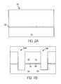
- FIG. 1Ais a top view of a semiconductor substrate used in the first step of the method of present invention to form isolation regions.
- FIG. 1Bis a cross sectional view of the structure taken along the line 1 B- 1 B showing the initial processing steps of the present invention.
- FIG. 1Cis a top view of the structure showing the next step in the processing of the structure of FIG. 1B , in which isolation regions are defined.
- FIG. 1Dis a cross sectional view of the structure in FIG. 1C taken along the line 1 D- 1 D showing the isolation trenches formed in the structure.
- FIG. 1Eis a cross sectional view of the structure in FIG. 1D showing the formation of isolation blocks of material in the isolation trenches.
- FIG. 1Fis a cross sectional view of the structure in FIG. 1E showing the final structure of the isolation regions.
- FIGS. 2A-2Pare cross sectional views of the semiconductor structure in FIG. 1F taken along the line 2 A- 2 A showing in sequence the steps in the processing of the semiconductor structure in the formation of a non-volatile memory array of floating gate memory cells of the present invention.
- FIG. 3is a schematic circuit diagram of the memory cell array of the present invention.
- FIGS. 1A to 1 F and 2 A to 2 Pshow the processing steps in making the memory cell array of the present invention.
- the methodbegins with a semiconductor substrate 10 , which is preferably of P type and is well known in the art.
- the thickness of the layers described belowwill depend upon the design rules and the process technology generation. What is described herein is for the 0.10 micron process. However, it will be understood by those skilled in the art that the present invention is not limited to any specific process technology generation, nor to any specific value in any of the process parameters described hereinafter.
- FIGS. 1A to 1 Fillustrate the Well known STI method of forming isolation regions on a substrate.
- a semiconductor substrate 10or a semiconductor well
- First and second layers of material 12 and 14are formed (e.g. grown or deposited) on the substrate.
- first layer 12can be silicon dioxide (hereinafter “oxide”), which is formed on the substrate 10 by any well known technique such as oxidation or oxide deposition (e.g. chemical vapor deposition or CVD) to a thickness of approximately 60-150 angstroms.
- Second layer 14can be silicon nitride (hereinafter “nitride”), which is formed over oxide layer 12 preferably by CVD to a thickness of approximately 1000-2000 angstroms.
- FIG. 1Billustrates a cross-section of the resulting structure.
- suitable photo resist material 16is applied on the nitride layer 14 and a masking step is performed to selectively remove the photo resist material from certain regions (stripes 18 ) that extend in the Y or column direction, as shown in FIG. 1C .
- the exposed nitride layer 14 and oxide layer 12are etched away in stripes 18 using standard etching techniques (i.e. anisotropic nitride and oxide etch processes) to form trenches 20 in the structure.
- the distance W between adjacent stripes 18can be as small as the smallest lithographic feature of the process used.
- a silicon etch processis then used to extend trenches 20 down into the silicon substrate 10 to a depth of approximately 500-4000 angstroms, as shown in FIG. 1D . Where the photo resist 16 is not removed, the nitride layer 14 and oxide layer 12 are maintained. The resulting structure illustrated in FIG. 1D now defines active regions 22 interlaced with isolation regions 24 .
- the structureis further processed to remove the remaining photo resist 16 .
- an isolation materialsuch as silicon dioxide is formed in trenches 20 by depositing a thick oxide layer, followed by a Chemical-Mechanical-Polishing or CMP etch (using nitride layer 14 as an etch stop) to remove the oxide layer except for oxide blocks 26 in trenches 20 , as shown in FIG. 1E .
- CMP etchusing nitride layer 14 as an etch stop
- the remaining nitride and oxide layers 14 / 12are then removed using nitride/oxide etch processes, leaving STI oxide blocks 26 extending along isolation regions 24 , as shown in FIG. 1F .
- FIGS. 1A to 1 Fillustrate the memory cell array region of the substrate, in which columns of memory cells will be formed in the active regions 22 which are separated by the isolation regions 24 .
- the substrate 10also includes at least one periphery region in which control circuitry is formed that will be used to operate the memory cells formed in the memory cell array region.
- isolation blocks 26are also formed in the periphery region during the same STI or LOCOS process described above.
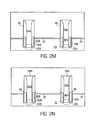
- FIGS. 2A to 2 Qshow the cross sections of the structure in the active regions 22 from a view orthogonal to that of FIG. 1F (along line 2 A- 2 A as shown in FIGS. 1C and 1F ).
- An insulation layer 30(preferably oxide) is first formed over the substrate 10 , as shown in FIG. 2A .
- the active region 22 portion of the substrate 10can be doped at this time for better independent control of the cell array portion of the memory device relative to the periphery region.
- Such dopingis often referred to as a Vt implant or cell well implant, and is well known in the art.
- the periphery regionis protected by a photo resist layer, which is deposited over the entire structure and removed from just the memory cell array region of the substrate.
- a thick layer of hard mask material 32such as nitride is formed over oxide layer 30 (e.g. ⁇ 3500 ⁇ thick).
- a plurality of parallel second trenches 34are formed in the nitride layer 32 by applying a photo resist (masking) material on the nitride layer 32 , and then performing a masking step to remove the photo resist material from selected parallel stripe regions.
- An anisotropic nitride etchis used to remove the exposed portions of nitride layer 32 in the stripe regions, leaving second trenches 34 that extend down to and expose oxide layer 30 .
- an anisotropic oxide etchis used to remove the exposed portions of oxide layer 30 and extend second trenches 34 down to the substrate 10 .
- a silicon anisotropic etch processis then used to extend second trenches 34 down into the substrate 10 in each of the active regions 22 (for example, down to a depth of approximately one feature size deep, e.g. about 0.15 um deep with 0.15 um technology).
- the photo resistcan be removed after trenches 34 are formed into the substrate 10 .
- the resulting active region 22is shown in FIG. 2B .
- a layer of insulation material 36is next formed (preferably using a thermal oxidation process) along the exposed silicon in second trenches 34 that forms the bottom and lower sidewalls of the second trenches 34 (e.g. ⁇ 70 ⁇ to 120 ⁇ thick).
- a thick layer of polysilicon 38(hereinafter “poly”) is then formed over the structure, which fills second trenches 34 .
- Poly layer 38can be doped (e.g. n+) by ion implant, or by an in-situ process.
- the resulting active region 22is shown in FIG. 2C .
- a poly etch process(e.g. a CMP process using nitride layer 32 as an etch stop) is used to remove poly layer 38 except for blocks 40 of the polysilicon 38 left remaining in second trenches 34 .
- a controlled poly etchis then used to lower the height of poly blocks 40 , where the tops of poly blocks 40 are disposed above the surface of the substrate, but below the tops of STI blocks 26 in the isolation regions 24 , as shown in FIG. 2D .
- Nitride spacers 44are then formed along the second trench sidewalls and over the sloped portions 42 of poly blocks 40 . Formation of spacers is well known in the art, and involves the deposition of a material over the contour of a structure, followed by an anisotropic etch process, whereby the material is removed from horizontal surfaces of the structure, while the material remains largely intact on vertically oriented surfaces of the structure. Spacers 44 can be formed of any dielectric material, such as oxide, nitride, etc.
- insulating spacers 44are formed by depositing a layer of nitride over the entire structure, followed by an anisotropic nitride etch process, such as the well known Reactive Ion Etch (RIE), to remove the deposited nitride layer except for spacers 44 .
- RIEReactive Ion Etch
- FIG. 2EIt should be noted that the formation of nitride spacers 44 is optional, as the spacers 44 are used to enhance the sharpness of the tips formed by the sloped portions 42 of poly blocks 40 . Thus, FIGS. 2F-2Q show the remaining processing steps without the optional nitride spacers 44 .
- a thermal oxidation processis then performed, which oxidizes the exposed top surfaces of the poly blocks 40 (forming oxide layer 46 thereon), as shown in FIG. 2F .
- Oxide spacers 48(shown in FIG. 2G ) are then formed along the sidewalls of the second trenches 34 by depositing oxide over the structure (e.g. approximately 350 ⁇ thickness) followed by an anisotropic oxide etch. The oxide etch also removes the center portion of oxide layer 46 in each of the second trenches 34 . The resulting active region 22 is shown in FIG. 2G .
- An anisotropic poly etchis next performed, which removes the center portions of the poly blocks 40 that are not protected by oxide spacers 48 , leaving a pair of opposing poly blocks 40 a in each of the second trenches 34 , as shown in FIG. 2H .
- An insulation deposition and anisotropic etch-back processis then used to form an insulation layer 50 along the exposed sides of poly blocks 40 a inside second trenches 34 (shown in FIG. 21 ).
- the insulation materialcould be any insulation material (e.g. ONO—oxide/nitride/oxide, or other high dielectric materials).
- the insulation materialis oxide, so that the oxide deposition/etch process also thickens the oxide spacers 48 and results in the removal of the exposed portions of oxide layer 36 at the bottom of each second trench 34 to expose the substrate 10 , as shown in FIG. 2J .
- the processalso removes the oxide in the STI between adjacent columns of active regions 22 in the trench 34 .
- Suitable ion implantationis then made across the surface of the structure to form first (source) regions 52 in the exposed substrate portions at the bottom of second trenches 34 .
- the source regions 52are self-aligned to the second trenches 34 and form a continuous row that is substantially perpendicular to the column of the active regions 22 , and have a second conductivity type (e.g. N type) that is different from a first conductivity type of the substrate (e.g. P type).
- the ionshave no significant effect on the nitride layer 32 .
- the resulting active region 22is shown in FIG. 2K .
- An oxidation deposition stepfollows and fills the bottom of each trench 34 with a layer of oxide 35 of approximately at least 100 angstroms, and no thicker than the height of the to-be-formed-floating gate-poly block 40 so that capacitive coupling between the to-be-deposited-and formed control gate 54 and the poly block 40 can occur.
- Thisis then followed by a poly deposition step, followed by a poly CMP etch (using the nitride layer 32 as an etch stop) are used to fill second trenches 34 with poly blocks 54 , as shown in FIG. 2L .
- the poly 54fills each trench 34 in a continuous row.
- a nitride etchfollows, which removes nitride layer 32 , and exposes upper edges of the poly blocks 40 a .
- a tunnel oxide layer 56is next formed on the exposed upper edges of poly blocks 40 a , either by thermal oxidation, oxide deposition, or both.
- This oxide formation stepalso forms an oxide layer 58 on the exposed top surfaces of poly blocks 54 , as well as possibly thickening oxide layer 30 over substrate 10 .
- Optional Vt implantation in the periphery regioncan be performed at this time by masking off the active regions 22 .
- the resulting active region 22is shown in FIGS. 2M and 2N .
- the oxide layer 30serves as the gate oxide for both the memory cells in the active regions, and the control circuitry in the periphery region.
- the thickness of the gate oxidedictate's its maximum operating voltage.
- photo resist 60is formed over the structure, followed by a masking step for selectively removing portions of the photo resist in the periphery region to expose portions of oxide layer 30 .
- the exposed portions of oxide layer 30can be thinned (e.g. by using a controlled etch) or replaced (e.g. by an oxide etch and oxide deposition) with oxide layer 30 a having the desired thickness, as illustrated in FIG. 2O .
- a poly deposition stepis used to form a poly layer 62 over the structure (e.g. approximately 500 ⁇ thick). Photo resist deposition and masking steps follow to form strips of poly layer 62 that are spaced apart from one another each over an active region 22 . The resulting active region 22 is shown in FIG. 2P . Each poly layer 62 functions as a word line for the memory array.
- the process of the present inventionforms an array of memory cells, with each memory cell 15 being between a pair of spaced apart source/drain regions 52 ( a,b ) (those skilled in the art would appreciated that the term source and drain may be interchanged during operation.)
- a non-planar channel regionconnects the two source regions 52 ( a,b ), with the channel region having three portions: a first portion, a second portion and a third portion.
- the first portion of the channel regionis along one of the sidewall of one of the trenches 34 , and is adjacent to the first source region 52 a .
- the second portion of the channel regionis along one of the sidewall of the other trench 34 , and is adjacent to the second source region 52 b .
- a third portion of the channel regionis between the first portion and the second portion and is substantially along the top surface of the substrate 10 .
- a dielectric layeris over the channel region. Over the first portion of the channel region, the dielectric is the layer 36 a . Over the second portion of the channel, the dielectric is the layer 36 b . Over the third portion of the channel region, the dielectric is the layer 30 .
- a first floating gate 40 ais on the layer 36 a , and is over the first portion of the channel region, which is adjacent to the first source region 52 a .
- a second floating gate 40 bis on the layer 36 b , and is over the second portion of the channel region, which is adjacent to the second source region 52 b .
- a gate electrode 62formed by the poly layer 62 , is over the dielectric layer 30 and is over the third portion of the channel region.
- a first control gate 54 ais insulated from the first source region 52 a , and is capacitively coupled to the first floating gate 40 a .
- a second control gate 54 bis insulated from the second source region 52 b , and is capacitively coupled to the second floating gate 40 b .
- each of the floating gates 40 a and 40 bis substantially perpendicular to the gate electrode 62 and to the surface of the substrate 10 .
- each source region, e.g. first source region 52 a , and its associated control gate, e.g. first control gate 54 ais shared with an adjacent memory cell 15 in the same active region 22 .
- the floating gates 40 ( a,b )are disposed in trenches 34 , with each floating gate facing and insulated from a portion of the channel region. Further, each floating gate 40 ( a,b ) includes an upper portion that extends above the substrate surface and terminates in an edge that faces and is insulated from one of the gate electrodes 62 , thus providing a path for Fowler-Nordheim tunneling through oxide layer 56 . Each control gate 54 extends along and are insulated (by oxide layer 50 ) from floating gates 44 , for enhanced voltage coupling therebetween.
- the interconnectionis as follows.
- the word line 62 that forms the gate electrode for each memory cell 15is extended in the Y direction to each of the memory cells 15 .
- the source lines 52 ( a,b ) and the associated control gates 54 ( a,b )extend continuously in the X direction to each of those memory cells 15 .
- memory cells 15 in adjacent rowsshare the same source region 52 and the same associated control gate 54 .
- Each of the memory cells 15has five independently controllable terminals: word line 62 , control gates 54 ( a,b ) and source regions 52 ( a,b ).
- lines 52 a , 52 b , 52 c etcare buried diffusion lines, and contacts must be made to those lines outside of the array of memory cells.
- One approachis to use a poly block 54 , similar to the control gate 54 , however, with the poly block 54 electrically contacting the buried diffusion lines 52 a , 52 b , 52 c etc. outside of the array. Further, the poly block 54 which contacts the buried diffusion lines 52 a , 52 b , 52 c , etc. outside of the array, must not be in electrical contact with the independent control gate 54 that is in the array.
- the memory cell 15is erased by applying 0 volts to the control gates 54 ( a,b ), and 0 volts to the source regions 52 ( a,b ). Since the same voltage is applied to both source regions 52 ( a,b ), no charges will conduct in the channel region. Furthermore, because the control gates 54 ( a,b ) are highly capacitively coupled to the floating gates 40 ( a,b ), the floating gates 40 ( a,b ) will experience a low voltage. A voltage of between 8 to 12 volts is applied to the word line 62 . This causes a large voltage differential between the floating gates 40 ( a,b ) and the word line 62 .
- Programming of the memory cell 15can occur in one of two mechanisms: either the first floating gate 40 a is programmed or the second floating gate 40 b is programmed.
- the first floating gate 40 ais programmed or the second floating gate 40 b is programmed.
- the first source region 52 ais held at a positive voltage of between 7 to 12 volts.
- the first control gate 54 ais held at a positive voltage of between 2 to 5 volts.
- the word line 62is held at a positive voltage of 1-3 volts.
- the second control gate 54 bis held at a positive voltage of between 1-2.5 volts.
- the second source region 52 bis held at 0 volts.
- the positive voltage of 1-2.5 volts on the second control gate 54 bis sufficient to turn on the second portion of the channel region, even if the second floating gate 40 b is programmed, i.e. has electrons stored thereon.
- the positive voltage of 1-2 volts on the word line 62is sufficient to turn on the third portion of the channel region.
- the positive voltage of 10-15 volts on the first source region 52 ais sufficient to attract the electrons in the channel.
- the positive voltage of 2 to 3 volts on the first control gate 54 ais sufficient to turn on the first portion of the channel region (because the first floating gate 40 a is erased).
- the voltages applied to the first control gate 54 a , first source region 52 aare reversed from those applied to the second control gate 54 b , and second source region 52 b.
- Reading of the memory cell 15can occur in one of two mechanisms: either the state of the first floating gate 40 a is read, or the state of the second floating gate 40 b is read. Let us first discuss the action of reading the state of the second floating gate 40 b , whether electrons are stored on the second floating gate 40 b .
- the first source region 52 ais held at a positive voltage of between 2 to 3.5 volts.
- the first control gate 54 ais held at a positive voltage of between 2 to 3 volts.
- the word line 62is held at a positive voltage of 2-3.5 volts.
- the second source region 52 bis held at 0 volts.
- the second control gate 54 bis held at a positive voltage of between 1-2.5 volts.
- the positive voltage of 2-3 volts on the first control gate 54 a , and the positive voltage of 2-3.5 volts on the first source region 52 aare sufficient to turn on the first portion of the channel region, even if the first floating gate 40 a is programmed, i.e. has electrons stored thereon.
- the positive voltage of 1.5-2.5 volts on the word line 62is sufficient to turn on the third portion of the channel region.
- the positive voltage of between 1 to 2.5 volt on the second control gate 54 bis sufficient to turn on the second portion of the channel region only if the second floating gate 40 b is not programmed. In that event, electrons will traverse in the channel region from the second source region 54 b to the first source region 54 a .
- the positive voltage of between 1 to 2.5 voltis not sufficient to turn on the second portion of the channel region. In that event, the channel remains non-conductive.
- the amount of current or the presence/absence of current sensed at the first source region 52 adetermines the state of programming of the second floating gate 40 b.
- the voltages applied to the first control gate 54 a and first source region 52 aare reversed from those applied to the second control gate 54 b and second source region 52 b.
- an array of memory cells 15comprises a plurality of memory cells arranged in a plurality of columns: 15 a ( 1 - k ), 15 b ( 1 - k ), and 15 c ( 1 - k ) and in rows: 15 ( a - n ) 1 , 15 ( a - n ) 2 and 15 ( a - n ) 3 .
- the word line 62 connected to a memory cell 15is also connected to other memory cells 15 in the same column.
- the first and second source regions 52 and the first and second control gates 54 connected to a memory cell 15are also connected to other memory cells in the same row.
- memory cells 15 in the same column connected by the common word line 62are erased simultaneously.
- the word line 2is held at between 8 to 12 volts.
- the unselected word lines 1 and 3are held at 0 volts.
- All the source region lines 52 and control gate lines 54are held at 0 volts. In this manner all of the memory cells 15 b ( 1 - n ) are erased simultaneously, while no erase disturbance occurs with respect to the memory cells 15 in the other columns because all five terminals to the memory cells 15 in all the other columns are at ground voltage.
- line 52 ais at a positive voltage of between 7 to 12 volts.
- Line 54 ais at a positive voltage of between 2 to 5 volts.
- Line 2is at a positive voltage of between 1-3 volts.
- Line 54 bis held at a positive voltage of 1-2.5 volts.
- Line 52 bis held at 0 volts.
- All the other unselected column lines, i.e. lines 1 and 3are at 0 volts.
- all the other row lines, such as 54 c , 54 d , and 52 c and 52 dare at 0 volts.
- the “disturbance” on the unselected memory cells 15are as follows:
- the application of 0 volts to lines 1 and 3means that none of the channel regions for those memory cells 15 c ( 1 - n ) and 15 a ( 1 - n ) are turned on, because the third portion of the channel region (the portion to which the word line 1 and 3 control) are not turned on. Thus, there is no disturbance.
- the application of 0 volts to line 54 cmeans that the portion of the channel region of the memory cell 15 b 2 which is adjacent to the source region 52 c will not be turned on. In that event the channel between the source region 52 c and the source region 52 b will be turned off.
- first control gate line 54 athe voltages applied to the first control gate line 54 a , first source region line 52 a are reversed from those applied to the second control gate line 54 b , and second source region line 52 b . All the other lines will have the same voltages as discussed for the programming of the first floating gate 40 a.
- the source region line 52 ais held at a positive voltage of between 2 to 3.5 volts.
- the first control gate line 54 ais held at a positive voltage between 2 to 3 volts.
- the word line 62 or line 2is held at a positive voltage of 2-3.5 volts.
- the second source region line 52 bis held at 0 volts.
- the second control gate line 54 bis held at a positive voltage of between 1-2.5 volts.
- the voltages applied to the unselected word lines 62 (lines 1 and 3 ) and the unselected source regions lines 52 c and 52 d , and the unselected control gate lines 54 c and 54 dare all held at ground or 0 volts.
- the “disturbance” on the unselected memory cells 15is as follows:
- the application of 0 volts to lines 1 and 3means that none of the channel regions for those memory cells 15 c ( 1 - k ) and 15 a ( 1 - k ) is turned on. Thus, there is no disturbance.
- the application of 0 volts to line 54 cmeans that the portion of the channel region of the memory cell 15 b 2 which is adjacent to the source region 52 c will not be turned on. In that event the channel region will be turned off. Thus, little or no disturbance to memory cell 15 b 2 would occur.
- first floating gate 40 aTo read the first floating gate 40 a , the voltages applied to the first control gate line 54 a , first source region line 52 a are reversed from those applied to the second control gate line 54 b , and second source region line 52 b . All the other lines will have the same voltages as discussed for the reading of the second floating gate 40 b.
- One unique feature of an array of memory cells 15 of the present inventionis the ability of the array to operate as a NAND device.
- a NAND devicehas a string of NVM connected in a serial fashion to a source of programming/read voltage. Let us assume that one string of NVM cells comprises: 15 b 1 , 15 b 2 , and 15 b 3 all in the same column connected by the same word line 62 .
- the erase operation for the string of NVM cells in the same stringis the same as that described previously for memory cells being erased in an array. Cells in the same column connected by the common word line 62 are erased simultaneously. Thus, cells in the same NAND string are erased simultaneously.
- a programming voltagesuch as 7-12 volts
- a “high” voltageis applied to the control gate 54 a , sufficient to “turn on” the channel adjacent the floating gate 40 a .
- a “high” voltage(1-3 volts) is applied to the word line 62 to “turn on” the channel between the floating gate 40 a and floating gate 40 b .
- a “high” voltage (2-5 volts)is applied to the control gate 54 b to turn on the channel adjacent to the floating gate 40 b .
- Thiscauses the entire channel region between the buried diffusion line 52 a and 52 b to be conducting.
- Buried diffusion line 52 bis held floating. This causes the programming voltage from diffusion line 52 a to be present at diffusion line 52 b .
- the “turning on” of the channel region for other cellscontinues until the programming voltage is at the buried diffusion line 52 c .
- a ground voltageis applied to buried diffusion line 52 d , which is at the other end of the chain of a string of NVM cells.
- a voltage of 1-2.5 voltsis applied to the control gate 54 d , which turns on the channel adjacent to the floating gate 40 f . Since the word line 62 is at a high voltage to turn on the channel region between the floating gate 40 f and floating gate 40 e , electrons traverse the channel region and are injected by hot channel electron injection onto the floating gate 40 e
- the programming voltageis first applied to the other end of the string of NVM cells, i.e. to diffusion line 52 d .
- Ground voltageis applied to diffusion line 52 a , and through the mechanism previously discussed, the ground voltage is transferred to diffusion line 52 c , which then causes hot channel electrons to program the floating gate 40 f.
- a read voltage of 2 to 3.5 voltsis applied to the diffusion line 52 d .
- Ground voltageis applied to diffusion line 52 a .
- a positive voltage, such as 1.5-3.5 voltsis applied to the word line 62 .
- a positive voltage such as 1 to 2.5 voltsis applied to each of the control gate 54 a , 54 b , and 54 c .
- the diffusion lines 52 b and 52 cwould receive the ground voltage from diffusion line 52 a . Electrons traversing from diffusion line 52 c to 52 d would be read and would be determinative of the state of the floating gate 40 e.
Landscapes
- Engineering & Computer Science (AREA)
- Microelectronics & Electronic Packaging (AREA)
- Non-Volatile Memory (AREA)
- Semiconductor Memories (AREA)
Abstract
Description
- The present invention relates to a bi-directional read/program non-volatile memory cell, that uses a floating gate for storage of charges. More particularly, the present invention relates to such non-volatile memory cell that has independent controllable control gates and is capable of storing a plurality of bits in a single cell and an array of such cells, and a method of manufacturing.
- Uni-directional read/program non-volatile memory cells using floating gate for storage are well known in the art. See for example, U.S. Pat. No. 5,029,130. Typically, each of these types of memory cells uses a conductive floating gate to store one bit, i.e. either the floating gate stores charges or it does not. The charges stored on a floating gate control the conduction of charges in a channel of a transistor. In a desire to increase the storage capacity of such non-volatile memory cells, the floating gate of such memory cell is programmed to store some charges, with the different amount of charges stored being determinative of the different states of the cell, thereby causing a plurality of bits to be stored in a single cell. The problem with programming a cell to one of a multilevel state and then reading such a state is that the amount of charge stored on the floating gate differentiating one state from another must be very carefully controlled.
- Bi-directional read/program non-volatile memory cells capable of storing a plurality of bits in a single cell are also well known in the art. See, for example, U.S. Pat. No. 6,011,725. Typically, these types of memory cells use an insulating trapping material, such as silicon nitride, which is between two other insulation layers, such as silicon dioxide, to trap charges. The charges are trapped near the source/drain also to control the conduction of charges in a channel of a transistor. The cell is read in one direction to determine the state of charges trapped near one of the source/drain regions, and is read in the opposite direction to determine the state of charges trapped near the other source/drain region. Hence, these cells are read and programmed bi-directionally. The problem with these types of cells is that to erase, holes or charges of the opposite conductivity must also be “programmed” or injected into the trapping material at precisely the same location where the programming charges were initially trapped in order to “neutralize” the programming charges. Since the programming charges and the erase charges are injected into a non-conductive trapping material, the charges do not move as in a conductive material. Therefore, if there is any error in injecting the erase charges to the location of the programming charges, the erase charges will not neutralize the programming charges, and the cell will not be completely erased. Moreover, to inject the erase charges, the cell must be erased bi-directionally, thereby increasing the time required for erasure of one cell.
- Hence there is a need for a non-volatile memory cell and array that overcomes these problems.
- In the present invention, a non-volatile memory cell for the storage of a plurality of bits comprises a substantially single crystalline semiconductive material, such as single crystalline silicon, of a first conductivity type. A first region of a second conductivity type, different from the first conductivity type is in the substrate. A second region of the second conductivity type is also in the substrate, spaced apart from the first region. A channel region, having a first portion, a second portion and a third portion, connects the first and second regions for the conduction of charges. A dielectric is on the channel region. A first floating gate is on the dielectric, spaced apart from the first portion of the channel region. The first portion of the channel region is adjacent to the first region. The first floating gate is for the storage of at least one of the plurality of bits. A second floating gate is on the dielectric, spaced apart from the second portion of the channel region. The second portion of the channel region is adjacent to the second region. The second floating gate is for the storage of at least another of the plurality of bits. A gate electrode is on the dielectric, spaced apart from the third portion of the channel region. The third portion of the channel region is between the first portion and the second portion. A first gate electrode is insulated from the first region and is also capacitively coupled to the first floating gate. A second gate electrode is insulated from the second region and is also capacitively coupled to the second floating gate.
- The present invention also relates to an array of the foregoing described non-volatile memory cells, and a method of making the non-volatile memory cell and the array.
FIG. 1A is a top view of a semiconductor substrate used in the first step of the method of present invention to form isolation regions.FIG. 1B is a cross sectional view of the structure taken along theline 1B-1B showing the initial processing steps of the present invention.FIG. 1C is a top view of the structure showing the next step in the processing of the structure ofFIG. 1B , in which isolation regions are defined.FIG. 1D is a cross sectional view of the structure inFIG. 1C taken along theline 1D-1D showing the isolation trenches formed in the structure.FIG. 1E is a cross sectional view of the structure inFIG. 1D showing the formation of isolation blocks of material in the isolation trenches.FIG. 1F is a cross sectional view of the structure inFIG. 1E showing the final structure of the isolation regions.FIGS. 2A-2P are cross sectional views of the semiconductor structure inFIG. 1F taken along theline 2A-2A showing in sequence the steps in the processing of the semiconductor structure in the formation of a non-volatile memory array of floating gate memory cells of the present invention.FIG. 3 is a schematic circuit diagram of the memory cell array of the present invention.- The method of the present invention is illustrated in
FIGS. 1A to1F and2A to2P, which show the processing steps in making the memory cell array of the present invention. The method begins with asemiconductor substrate 10, which is preferably of P type and is well known in the art. The thickness of the layers described below will depend upon the design rules and the process technology generation. What is described herein is for the 0.10 micron process. However, it will be understood by those skilled in the art that the present invention is not limited to any specific process technology generation, nor to any specific value in any of the process parameters described hereinafter. - Isolation Region Formation
FIGS. 1A to1F illustrate the Well known STI method of forming isolation regions on a substrate. Referring toFIG. 1A there is shown a top plan view of a semiconductor substrate10 (or a semiconductor well), which is preferably of P type and is well known in the art. First and second layers ofmaterial first layer 12 can be silicon dioxide (hereinafter “oxide”), which is formed on thesubstrate 10 by any well known technique such as oxidation or oxide deposition (e.g. chemical vapor deposition or CVD) to a thickness of approximately 60-150 angstroms.Second layer 14 can be silicon nitride (hereinafter “nitride”), which is formed overoxide layer 12 preferably by CVD to a thickness of approximately 1000-2000 angstroms.FIG. 1B illustrates a cross-section of the resulting structure.- Once the first and
second layers 12/14 have been formed, suitable photo resistmaterial 16 is applied on thenitride layer 14 and a masking step is performed to selectively remove the photo resist material from certain regions (stripes18) that extend in the Y or column direction, as shown inFIG. 1C . Where the photo-resistmaterial 16 is removed, the exposednitride layer 14 andoxide layer 12 are etched away instripes 18 using standard etching techniques (i.e. anisotropic nitride and oxide etch processes) to formtrenches 20 in the structure. The distance W betweenadjacent stripes 18 can be as small as the smallest lithographic feature of the process used. A silicon etch process is then used to extendtrenches 20 down into thesilicon substrate 10 to a depth of approximately 500-4000 angstroms, as shown inFIG. 1D . Where the photo resist16 is not removed, thenitride layer 14 andoxide layer 12 are maintained. The resulting structure illustrated inFIG. 1D now definesactive regions 22 interlaced withisolation regions 24. - The structure is further processed to remove the remaining photo resist16. Then, an isolation material such as silicon dioxide is formed in
trenches 20 by depositing a thick oxide layer, followed by a Chemical-Mechanical-Polishing or CMP etch (usingnitride layer 14 as an etch stop) to remove the oxide layer except for oxide blocks26 intrenches 20, as shown inFIG. 1E . The remaining nitride andoxide layers 14/12 are then removed using nitride/oxide etch processes, leaving STI oxide blocks26 extending alongisolation regions 24, as shown inFIG. 1F . - The STI isolation method described above is the preferred method of forming
isolation regions 24. However, the well known LOCOS isolation method (e.g. recessed LOCOS, poly buffered LOCOS, etc.) could alternately be used, where thetrenches 20 may not extend into the substrate, and isolation material may be formed on the substrate surface instripe regions 18.FIGS. 1A to1F illustrate the memory cell array region of the substrate, in which columns of memory cells will be formed in theactive regions 22 which are separated by theisolation regions 24. It should be noted that thesubstrate 10 also includes at least one periphery region in which control circuitry is formed that will be used to operate the memory cells formed in the memory cell array region. Preferably, isolation blocks26 are also formed in the periphery region during the same STI or LOCOS process described above. - Memory Cell Formation
- The structure shown in
FIG. 1F is further processed as follows.FIGS. 2A to2Q show the cross sections of the structure in theactive regions 22 from a view orthogonal to that ofFIG. 1F (alongline 2A-2A as shown inFIGS. 1C and 1F ). - An insulation layer30 (preferably oxide) is first formed over the
substrate 10, as shown inFIG. 2A . Theactive region 22 portion of thesubstrate 10 can be doped at this time for better independent control of the cell array portion of the memory device relative to the periphery region. Such doping is often referred to as a Vt implant or cell well implant, and is well known in the art. During this implant, the periphery region is protected by a photo resist layer, which is deposited over the entire structure and removed from just the memory cell array region of the substrate. - Next, a thick layer of
hard mask material 32 such as nitride is formed over oxide layer30 (e.g. ˜3500 Å thick). A plurality of parallel second trenches34 are formed in thenitride layer 32 by applying a photo resist (masking) material on thenitride layer 32, and then performing a masking step to remove the photo resist material from selected parallel stripe regions. An anisotropic nitride etch is used to remove the exposed portions ofnitride layer 32 in the stripe regions, leaving second trenches34 that extend down to and exposeoxide layer 30. After the photo resist is removed, an anisotropic oxide etch is used to remove the exposed portions ofoxide layer 30 and extend second trenches34 down to thesubstrate 10. A silicon anisotropic etch process is then used to extend second trenches34 down into thesubstrate 10 in each of the active regions22 (for example, down to a depth of approximately one feature size deep, e.g. about 0.15 um deep with 0.15 um technology). Alternately, the photo resist can be removed after trenches34 are formed into thesubstrate 10. The resultingactive region 22 is shown inFIG. 2B . - A layer of insulation material36 is next formed (preferably using a thermal oxidation process) along the exposed silicon in second trenches34 that forms the bottom and lower sidewalls of the second trenches34 (e.g. ˜70 Å to 120 Å thick). A thick layer of polysilicon38 (hereinafter “poly”) is then formed over the structure, which fills second trenches34.
Poly layer 38 can be doped (e.g. n+) by ion implant, or by an in-situ process. The resultingactive region 22 is shown inFIG. 2C . - A poly etch process (e.g. a CMP process using
nitride layer 32 as an etch stop) is used to removepoly layer 38 except for blocks40 of thepolysilicon 38 left remaining in second trenches34. A controlled poly etch is then used to lower the height of poly blocks40, where the tops of poly blocks40 are disposed above the surface of the substrate, but below the tops of STI blocks26 in theisolation regions 24, as shown inFIG. 2D . - Another poly etch is then performed to create sloped
portions 42 on the tops of poly blocks40 (adjacent the second trench sidewalls).Nitride spacers 44 are then formed along the second trench sidewalls and over thesloped portions 42 of poly blocks40. Formation of spacers is well known in the art, and involves the deposition of a material over the contour of a structure, followed by an anisotropic etch process, whereby the material is removed from horizontal surfaces of the structure, while the material remains largely intact on vertically oriented surfaces of the structure.Spacers 44 can be formed of any dielectric material, such as oxide, nitride, etc. In the present embodiment, insulatingspacers 44 are formed by depositing a layer of nitride over the entire structure, followed by an anisotropic nitride etch process, such as the well known Reactive Ion Etch (RIE), to remove the deposited nitride layer except forspacers 44. The resultingactive region 22 is shown inFIG. 2E . It should be noted that the formation ofnitride spacers 44 is optional, as thespacers 44 are used to enhance the sharpness of the tips formed by the slopedportions 42 of poly blocks40. Thus,FIGS. 2F-2Q show the remaining processing steps without theoptional nitride spacers 44. - A thermal oxidation process is then performed, which oxidizes the exposed top surfaces of the poly blocks40 (forming
oxide layer 46 thereon), as shown inFIG. 2F . Oxide spacers48 (shown inFIG. 2G ) are then formed along the sidewalls of the second trenches34 by depositing oxide over the structure (e.g. approximately 350 Å thickness) followed by an anisotropic oxide etch. The oxide etch also removes the center portion ofoxide layer 46 in each of the second trenches34. The resultingactive region 22 is shown inFIG. 2G . - An anisotropic poly etch is next performed, which removes the center portions of the poly blocks40 that are not protected by
oxide spacers 48, leaving a pair of opposing poly blocks40ain each of the second trenches34, as shown inFIG. 2H . An insulation deposition and anisotropic etch-back process is then used to form aninsulation layer 50 along the exposed sides of poly blocks40ainside second trenches34 (shown inFIG. 21 ). The insulation material could be any insulation material (e.g. ONO—oxide/nitride/oxide, or other high dielectric materials). Preferably, the insulation material is oxide, so that the oxide deposition/etch process also thickens theoxide spacers 48 and results in the removal of the exposed portions of oxide layer36 at the bottom of each second trench34 to expose thesubstrate 10, as shown inFIG. 2J . In addition, when the oxide layer36 at the bottom of each trench34 is removed, the process also removes the oxide in the STI between adjacent columns ofactive regions 22 in the trench34. - Suitable ion implantation (and possible anneal) is then made across the surface of the structure to form first (source) regions52 in the exposed substrate portions at the bottom of second trenches34. The source regions52 are self-aligned to the second trenches34 and form a continuous row that is substantially perpendicular to the column of the
active regions 22, and have a second conductivity type (e.g. N type) that is different from a first conductivity type of the substrate (e.g. P type). The ions have no significant effect on thenitride layer 32. The resultingactive region 22 is shown inFIG. 2K . - An oxidation deposition step follows and fills the bottom of each trench34 with a layer of
oxide 35 of approximately at least 100 angstroms, and no thicker than the height of the to-be-formed-floating gate-poly block40 so that capacitive coupling between the to-be-deposited-and formed control gate54 and the poly block40 can occur. This is then followed by a poly deposition step, followed by a poly CMP etch (using thenitride layer 32 as an etch stop) are used to fill second trenches34 with poly blocks54, as shown inFIG. 2L . Thus, the poly54 fills each trench34 in a continuous row. A nitride etch follows, which removesnitride layer 32, and exposes upper edges of the poly blocks40a. Atunnel oxide layer 56 is next formed on the exposed upper edges of poly blocks40a, either by thermal oxidation, oxide deposition, or both. This oxide formation step also forms anoxide layer 58 on the exposed top surfaces of poly blocks54, as well as possibly thickeningoxide layer 30 oversubstrate 10. Optional Vt implantation in the periphery region can be performed at this time by masking off theactive regions 22. The resultingactive region 22 is shown inFIGS. 2M and 2N . - The
oxide layer 30 serves as the gate oxide for both the memory cells in the active regions, and the control circuitry in the periphery region. For each device, the thickness of the gate oxide dictate's its maximum operating voltage. Thus, if it is desired that some of the control circuitry operate at a different voltage than the memory cells or other devices of the control circuitry, then the thickness of thegate oxide 32 can be modified at this point in the process. In way of example but not limitation, photo resist60 is formed over the structure, followed by a masking step for selectively removing portions of the photo resist in the periphery region to expose portions ofoxide layer 30. The exposed portions ofoxide layer 30 can be thinned (e.g. by using a controlled etch) or replaced (e.g. by an oxide etch and oxide deposition) with oxide layer30ahaving the desired thickness, as illustrated inFIG. 2O . - After removal of photo resist60, a poly deposition step is used to form a
poly layer 62 over the structure (e.g. approximately 500 Å thick). Photo resist deposition and masking steps follow to form strips ofpoly layer 62 that are spaced apart from one another each over anactive region 22. The resultingactive region 22 is shown inFIG. 2P . Eachpoly layer 62 functions as a word line for the memory array. - As shown in
FIG. 2P , the process of the present invention forms an array of memory cells, with eachmemory cell 15 being between a pair of spaced apart source/drain regions52(a,b) (those skilled in the art would appreciated that the term source and drain may be interchanged during operation.) A non-planar channel region connects the two source regions52(a,b), with the channel region having three portions: a first portion, a second portion and a third portion. The first portion of the channel region is along one of the sidewall of one of the trenches34, and is adjacent to thefirst source region 52a. The second portion of the channel region is along one of the sidewall of the other trench34, and is adjacent to thesecond source region 52b. A third portion of the channel region is between the first portion and the second portion and is substantially along the top surface of thesubstrate 10. A dielectric layer is over the channel region. Over the first portion of the channel region, the dielectric is thelayer 36a. Over the second portion of the channel, the dielectric is thelayer 36b. Over the third portion of the channel region, the dielectric is thelayer 30. A first floatinggate 40ais on thelayer 36a, and is over the first portion of the channel region, which is adjacent to thefirst source region 52a. A second floatinggate 40bis on thelayer 36b, and is over the second portion of the channel region, which is adjacent to thesecond source region 52b. Agate electrode 62, formed by thepoly layer 62, is over thedielectric layer 30 and is over the third portion of the channel region. Afirst control gate 54ais insulated from thefirst source region 52a, and is capacitively coupled to the first floatinggate 40a. Asecond control gate 54bis insulated from thesecond source region 52b, and is capacitively coupled to the second floatinggate 40b. Further, each of the floatinggates gate electrode 62 and to the surface of thesubstrate 10. Finally, each source region, e.g.first source region 52a, and its associated control gate, e.g.first control gate 54ais shared with anadjacent memory cell 15 in the sameactive region 22. - The floating gates40 (a,b) are disposed in trenches34, with each floating gate facing and insulated from a portion of the channel region. Further, each floating gate40 (a,b) includes an upper portion that extends above the substrate surface and terminates in an edge that faces and is insulated from one of the
gate electrodes 62, thus providing a path for Fowler-Nordheim tunneling throughoxide layer 56. Each control gate54 extends along and are insulated (by oxide layer50) from floatinggates 44, for enhanced voltage coupling therebetween. - With respect to the plurality of
memory cells 15 that form an array, the interconnection is as follows. Formemory cells 15 that are in the same column, i.e. in the sameactive region 22, theword line 62 that forms the gate electrode for eachmemory cell 15 is extended in the Y direction to each of thememory cells 15. Formemory cells 15 that are in the same row, i.e. across theactive regions 22 and theSTI 26, the source lines52 (a,b) and the associated control gates54 (a,b) extend continuously in the X direction to each of thosememory cells 15. Finally, as can be seen from the foregoing,memory cells 15 in adjacent rows, share the same source region52 and the same associated control gate54. Each of thememory cells 15 has five independently controllable terminals:word line 62, control gates54 (a,b) and source regions52 (a,b). - As will be appreciated by those skilled in the art, lines52a,52b,52cetc, are buried diffusion lines, and contacts must be made to those lines outside of the array of memory cells. One approach is to use a poly block54, similar to the control gate54, however, with the poly block54 electrically contacting the buried
diffusion lines diffusion lines - Memory Cell Operation
- The operation of the
memory cell 15 shown inFIG. 2P will now be described. - Erase
- The
memory cell 15 is erased by applying 0 volts to the control gates54(a,b), and 0 volts to the source regions52(a,b). Since the same voltage is applied to both source regions52(a,b), no charges will conduct in the channel region. Furthermore, because the control gates54(a,b) are highly capacitively coupled to the floating gates40(a,b), the floating gates40(a,b) will experience a low voltage. A voltage of between 8 to 12 volts is applied to theword line 62. This causes a large voltage differential between the floating gates40(a,b) and theword line 62. Any electrons stored on the floating gates40(a,b) are pulled by the positive voltage applied to theword line 62, and through the mechanism of Fowler-Nordheim tunneling, the electrons are removed from the floating gates40(a,b), and tunnel through thetunneling oxide 56 onto theword line 62. This mechanism of poly-to-poly tunneling for erase is set forth in U.S. Pat. No. 5,029,130, whose disclosure is incorporated herein in its entirety by reference. - Programming
- Programming of the
memory cell 15 can occur in one of two mechanisms: either the first floatinggate 40ais programmed or the second floatinggate 40bis programmed. Let us first discuss the action of programming the first floatinggate 40a, i.e. storage of electrons on the first floatinggate 40a. Thefirst source region 52ais held at a positive voltage of between 7 to 12 volts. Thefirst control gate 54ais held at a positive voltage of between 2 to 5 volts. Theword line 62 is held at a positive voltage of 1-3 volts. Thesecond control gate 54bis held at a positive voltage of between 1-2.5 volts. Thesecond source region 52bis held at 0 volts. Because thesecond control gate 54bis strongly capacitively coupled to the second floatinggate 40b, the positive voltage of 1-2.5 volts on thesecond control gate 54bis sufficient to turn on the second portion of the channel region, even if the second floatinggate 40bis programmed, i.e. has electrons stored thereon. The positive voltage of 1-2 volts on theword line 62 is sufficient to turn on the third portion of the channel region. The positive voltage of 10-15 volts on thefirst source region 52ais sufficient to attract the electrons in the channel. The positive voltage of 2 to 3 volts on thefirst control gate 54ais sufficient to turn on the first portion of the channel region (because the first floatinggate 40ais erased). Thus, electrons will traverse in the channel region from thesecond source region 54bto thefirst source region 54a. However, at the junction in the channel region where the channel region takes substantially a 90 degree turn in the direction from the planar surface to thefirst trench 34a, the electrons will experience a sudden increase in voltage, caused by the positive high voltage of thefirst source region 54a. This causes the electrons to be hot channel injected onto the first floatinggate 40a. This mechanism of hot channel electron injection for programming is set forth in U.S. Pat. No. 5,029,130, whose disclosure is incorporated herein in its entirety by reference. - To program the second floating
gate 40b, the voltages applied to thefirst control gate 54a,first source region 52aare reversed from those applied to thesecond control gate 54b, andsecond source region 52b. - Read
- Reading of the
memory cell 15 can occur in one of two mechanisms: either the state of the first floatinggate 40ais read, or the state of the second floatinggate 40bis read. Let us first discuss the action of reading the state of the second floatinggate 40b, whether electrons are stored on the second floatinggate 40b. Thefirst source region 52ais held at a positive voltage of between 2 to 3.5 volts. Thefirst control gate 54ais held at a positive voltage of between 2 to 3 volts. Theword line 62 is held at a positive voltage of 2-3.5 volts. Thesecond source region 52bis held at 0 volts. Thesecond control gate 54bis held at a positive voltage of between 1-2.5 volts. The positive voltage of 2-3 volts on thefirst control gate 54a, and the positive voltage of 2-3.5 volts on thefirst source region 52aare sufficient to turn on the first portion of the channel region, even if the first floatinggate 40ais programmed, i.e. has electrons stored thereon. The positive voltage of 1.5-2.5 volts on theword line 62 is sufficient to turn on the third portion of the channel region. The positive voltage of between 1 to 2.5 volt on thesecond control gate 54bis sufficient to turn on the second portion of the channel region only if the second floatinggate 40bis not programmed. In that event, electrons will traverse in the channel region from thesecond source region 54bto thefirst source region 54a. However, if the second floatinggate 40bis programmed, then the positive voltage of between 1 to 2.5 volt is not sufficient to turn on the second portion of the channel region. In that event, the channel remains non-conductive. Thus, the amount of current or the presence/absence of current sensed at thefirst source region 52adetermines the state of programming of the second floatinggate 40b. - To read the first floating
gate 40a, the voltages applied to thefirst control gate 54aandfirst source region 52aare reversed from those applied to thesecond control gate 54bandsecond source region 52b. - Memory Cell Array Operation
- The operation of an array of
memory cells 15 will now be described. Schematically, an array of memory cells is shown inFIG. 3 . As shown inFIG. 3 , an array ofmemory cells 15 comprises a plurality of memory cells arranged in a plurality of columns:15a(1-k),15b(1-k), and15c(1-k) and in rows:15(a-n)1,15(a-n)2 and15(a-n)3. Theword line 62 connected to amemory cell 15 is also connected toother memory cells 15 in the same column. The first and second source regions52 and the first and second control gates54 connected to amemory cell 15 are also connected to other memory cells in the same row. - Erase
- In the erase operation,
memory cells 15 in the same column connected by thecommon word line 62 are erased simultaneously. Thus, for example, if it is desired to erasememory cells 15 in the column15b(1-n), theword line 2 is held at between 8 to 12 volts. Theunselected word lines memory cells 15 in the other columns because all five terminals to thememory cells 15 in all the other columns are at ground voltage. - Program
- Let us assume that the first floating
gate 40aof the memory cell15b 1 is to be programmed. Then based upon the foregoing discussion, the voltages applied to the various lines are as follows:line 52ais at a positive voltage of between 7 to 12 volts.Line 54ais at a positive voltage of between 2 to 5 volts.Line 2 is at a positive voltage of between 1-3 volts.Line 54bis held at a positive voltage of 1-2.5 volts.Line 52bis held at 0 volts. All the other unselected column lines, i.e.lines unselected memory cells 15 are as follows: - For the
memory cells 15 in the unselected column, the application of 0 volts tolines word line b 2 which is in the same selected column, but in an unselected row, the application of 0 volts to line54cmeans that the portion of the channel region of the memory cell15b 2 which is adjacent to the source region52cwill not be turned on. In that event the channel between the source region52cand thesource region 52bwill be turned off. Thus, little or no disturbance to memory cell15b 2 would occur. Similarly for allother memory cells 15 in the selected column but unselected row, a portion of the channel region of those memory cells will not be turned on due to the 0 volts being applied to the unselected control gates54. - To program the second floating
gate 40b, the voltages applied to the firstcontrol gate line 54a, firstsource region line 52aare reversed from those applied to the secondcontrol gate line 54b, and secondsource region line 52b. All the other lines will have the same voltages as discussed for the programming of the first floatinggate 40a. - Read
- Let us assume that the second floating
gate 40bof the memory cell15b 1 is to be read. Then based upon the foregoing discussion, the voltages applied to the various lines are as follows: Thesource region line 52ais held at a positive voltage of between 2 to 3.5 volts. The firstcontrol gate line 54ais held at a positive voltage between 2 to 3 volts. Theword line 62 orline 2 is held at a positive voltage of 2-3.5 volts. The secondsource region line 52bis held at 0 volts. The secondcontrol gate line 54bis held at a positive voltage of between 1-2.5 volts. - The voltages applied to the unselected word lines62 (
lines 1 and3) and the unselected source regions lines52cand52d, and the unselectedcontrol gate lines 54cand54dare all held at ground or 0 volts. The “disturbance” on theunselected memory cells 15 is as follows: - For the
memory cells 15 in the unselected columns, the application of 0 volts tolines b 2 which is in the same selected column, but in an unselected row, the application of 0 volts to line54cmeans that the portion of the channel region of the memory cell15b 2 which is adjacent to the source region52cwill not be turned on. In that event the channel region will be turned off. Thus, little or no disturbance to memory cell15b 2 would occur. Similarly, for all the other memory cells in the same selected column but unselected rows, there will not be any disturbance. - To read the first floating
gate 40a, the voltages applied to the firstcontrol gate line 54a, firstsource region line 52aare reversed from those applied to the secondcontrol gate line 54b, and secondsource region line 52b. All the other lines will have the same voltages as discussed for the reading of the second floatinggate 40b. - NAND Operation
- One unique feature of an array of
memory cells 15 of the present invention is the ability of the array to operate as a NAND device. A NAND device has a string of NVM connected in a serial fashion to a source of programming/read voltage. Let us assume that one string of NVM cells comprises:15b 1,15b 2, and15b3 all in the same column connected by thesame word line 62. - Erase
- The erase operation for the string of NVM cells in the same string is the same as that described previously for memory cells being erased in an array. Cells in the same column connected by the
common word line 62 are erased simultaneously. Thus, cells in the same NAND string are erased simultaneously. - Program
- To program a particular cell, in a string of NVM cells,
e.g. floating gate 40eof cell15b 3 in a string of NVM cells comprising cells15b(1-3), the various voltages applied are as follows: A programming voltage, such as 7-12 volts, is first applied at burieddiffusion line 52a. A “high” voltage is applied to thecontrol gate 54a, sufficient to “turn on” the channel adjacent the floatinggate 40a. A “high” voltage (1-3 volts) is applied to theword line 62 to “turn on” the channel between the floatinggate 40aand floatinggate 40b. A “high” voltage (2-5 volts) is applied to thecontrol gate 54bto turn on the channel adjacent to the floatinggate 40b. This causes the entire channel region between the burieddiffusion line Buried diffusion line 52bis held floating. This causes the programming voltage fromdiffusion line 52ato be present atdiffusion line 52b. The “turning on” of the channel region for other cells continues until the programming voltage is at the buried diffusion line52c. A ground voltage is applied to burieddiffusion line 52d, which is at the other end of the chain of a string of NVM cells. A voltage of 1-2.5 volts is applied to thecontrol gate 54d, which turns on the channel adjacent to the floatinggate 40f. Since theword line 62 is at a high voltage to turn on the channel region between the floatinggate 40fand floatinggate 40e, electrons traverse the channel region and are injected by hot channel electron injection onto the floatinggate 40e. - To program the floating
gate 40fof memory cell15b 3, the programming voltage is first applied to the other end of the string of NVM cells, i.e. todiffusion line 52d. Ground voltage is applied todiffusion line 52a, and through the mechanism previously discussed, the ground voltage is transferred to diffusion line52c, which then causes hot channel electrons to program the floatinggate 40f. - Read
- To read a particular cell, in a string of NVM cells,
e.g. floating gate 40eof cell15b 3 in a string of NVM cells comprising cells15b(1-3), the various voltages applied are as follows: A read voltage of 2 to 3.5 volts is applied to thediffusion line 52d. Ground voltage is applied todiffusion line 52a. A positive voltage, such as 1.5-3.5 volts is applied to theword line 62. A positive voltage such as 1 to 2.5 volts is applied to each of thecontrol gate diffusion lines 52band52cwould receive the ground voltage fromdiffusion line 52a. Electrons traversing from diffusion line52cto52dwould be read and would be determinative of the state of the floatinggate 40e. - From the foregoing it can be seen that a novel, high density non-volatile memory cell, array and method of manufacturing is disclosed. It should be appreciated that although the preferred embodiment has been described in which a single bit is stored in each of the two floating gates in a memory cell, it is also within the spirit of the present invention to store multi-bits on each one of the floating gates in a single memory cell, thereby increasing further the density of storage.
Claims (10)
Priority Applications (1)
| Application Number | Priority Date | Filing Date | Title |
|---|---|---|---|
| US11/521,162US7205198B2 (en) | 2003-04-07 | 2006-09-14 | Method of making a bi-directional read/program non-volatile floating gate memory cell |
Applications Claiming Priority (2)
| Application Number | Priority Date | Filing Date | Title |
|---|---|---|---|
| US10/409,407US7190018B2 (en) | 2003-04-07 | 2003-04-07 | Bi-directional read/program non-volatile floating gate memory cell with independent controllable control gates, and array thereof, and method of formation |
| US11/521,162US7205198B2 (en) | 2003-04-07 | 2006-09-14 | Method of making a bi-directional read/program non-volatile floating gate memory cell |
Related Parent Applications (1)
| Application Number | Title | Priority Date | Filing Date |
|---|---|---|---|
| US10/409,407DivisionUS7190018B2 (en) | 2003-04-07 | 2003-04-07 | Bi-directional read/program non-volatile floating gate memory cell with independent controllable control gates, and array thereof, and method of formation |
Publications (2)
| Publication Number | Publication Date |
|---|---|
| US20070020854A1true US20070020854A1 (en) | 2007-01-25 |
| US7205198B2 US7205198B2 (en) | 2007-04-17 |
Family
ID=33097833
Family Applications (2)
| Application Number | Title | Priority Date | Filing Date |
|---|---|---|---|
| US10/409,407Expired - LifetimeUS7190018B2 (en) | 2003-04-07 | 2003-04-07 | Bi-directional read/program non-volatile floating gate memory cell with independent controllable control gates, and array thereof, and method of formation |
| US11/521,162Expired - LifetimeUS7205198B2 (en) | 2003-04-07 | 2006-09-14 | Method of making a bi-directional read/program non-volatile floating gate memory cell |
Family Applications Before (1)
| Application Number | Title | Priority Date | Filing Date |
|---|---|---|---|
| US10/409,407Expired - LifetimeUS7190018B2 (en) | 2003-04-07 | 2003-04-07 | Bi-directional read/program non-volatile floating gate memory cell with independent controllable control gates, and array thereof, and method of formation |
Country Status (5)
| Country | Link |
|---|---|
| US (2) | US7190018B2 (en) |
| JP (1) | JP2004312021A (en) |
| KR (1) | KR20040087930A (en) |
| CN (1) | CN1536675A (en) |
| TW (1) | TW200503252A (en) |
Families Citing this family (19)
| Publication number | Priority date | Publication date | Assignee | Title |
|---|---|---|---|---|
| US7613041B2 (en)* | 2003-06-06 | 2009-11-03 | Chih-Hsin Wang | Methods for operating semiconductor device and semiconductor memory device |
| US7759719B2 (en)* | 2004-07-01 | 2010-07-20 | Chih-Hsin Wang | Electrically alterable memory cell |
| US7550800B2 (en)* | 2003-06-06 | 2009-06-23 | Chih-Hsin Wang | Method and apparatus transporting charges in semiconductor device and semiconductor memory device |
| US20080203464A1 (en)* | 2004-07-01 | 2008-08-28 | Chih-Hsin Wang | Electrically alterable non-volatile memory and array |
| CN100378961C (en)* | 2005-04-18 | 2008-04-02 | 力晶半导体股份有限公司 | Method for manufacturing non-volatile memory |
| TWI270977B (en)* | 2005-06-27 | 2007-01-11 | Powerchip Semiconductor Corp | Non-volatile memory and manufacturing method and operating method thereof |
| US7411244B2 (en)* | 2005-06-28 | 2008-08-12 | Chih-Hsin Wang | Low power electrically alterable nonvolatile memory cells and arrays |
| US7586145B2 (en)* | 2005-07-27 | 2009-09-08 | Taiwan Semiconductor Manufacturing Co. Ltd | EEPROM flash memory device with jagged edge floating gate |
| US7130221B1 (en)* | 2005-09-26 | 2006-10-31 | Macronix International Co., Ltd. | Dual gate multi-bit semiconductor memory |
| US7759727B2 (en)* | 2006-08-21 | 2010-07-20 | Intersil Americas Inc. | Method and apparatus for shielding tunneling circuit and floating gate for integration of a floating gate voltage reference in a general purpose CMOS technology |
| US8384149B2 (en)* | 2007-04-19 | 2013-02-26 | Taiwan Semiconductor Manufacturing Company, Ltd | Memory cell having a shared programming gate |
| US7800159B2 (en)* | 2007-10-24 | 2010-09-21 | Silicon Storage Technology, Inc. | Array of contactless non-volatile memory cells |
| US8072023B1 (en) | 2007-11-12 | 2011-12-06 | Marvell International Ltd. | Isolation for non-volatile memory cell array |
| US8120088B1 (en) | 2007-12-07 | 2012-02-21 | Marvell International Ltd. | Non-volatile memory cell and array |
| CN101582454B (en)* | 2008-05-16 | 2011-03-16 | 南亚科技股份有限公司 | Double-bit U-shaped memory structure and manufacturing method thereof |
| US7826267B2 (en)* | 2008-05-23 | 2010-11-02 | Silicon Storage Technology, Inc. | Method and apparatus for reading and programming a non-volatile memory cell in a virtual ground array |
| KR102128718B1 (en)* | 2018-09-05 | 2020-07-02 | 고려대학교 산학협력단 | Transposable feedback field-effect electronic device and array using the same |
| CN113113384B (en)* | 2021-03-18 | 2022-04-01 | 长鑫存储技术有限公司 | Semiconductor structure and manufacturing method thereof |
| CN113066763B (en)* | 2021-03-24 | 2022-04-26 | 长鑫存储技术有限公司 | Semiconductor structure and manufacturing method thereof |
Citations (20)
| Publication number | Priority date | Publication date | Assignee | Title |
|---|---|---|---|---|
| US5021999A (en)* | 1987-12-17 | 1991-06-04 | Mitsubishi Denki Kabushiki Kaisha | Non-volatile semiconductor memory device with facility of storing tri-level data |
| US5029130A (en)* | 1990-01-22 | 1991-07-02 | Silicon Storage Technology, Inc. | Single transistor non-valatile electrically alterable semiconductor memory device |
| US5739567A (en)* | 1992-11-02 | 1998-04-14 | Wong; Chun Chiu D. | Highly compact memory device with nonvolatile vertical transistor memory cell |
| US5768192A (en)* | 1996-07-23 | 1998-06-16 | Saifun Semiconductors, Ltd. | Non-volatile semiconductor memory cell utilizing asymmetrical charge trapping |
| US6002152A (en)* | 1992-01-14 | 1999-12-14 | Sandisk Corporation | EEPROM with split gate source side injection with sidewall spacers |
| US6011725A (en)* | 1997-08-01 | 2000-01-04 | Saifun Semiconductors, Ltd. | Two bit non-volatile electrically erasable and programmable semiconductor memory cell utilizing asymmetrical charge trapping |
| US6074914A (en)* | 1998-10-30 | 2000-06-13 | Halo Lsi Design & Device Technology, Inc. | Integration method for sidewall split gate flash transistor |
| US6093945A (en)* | 1998-07-09 | 2000-07-25 | Windbond Electronics Corp. | Split gate flash memory with minimum over-erase problem |
| US6103573A (en)* | 1999-06-30 | 2000-08-15 | Sandisk Corporation | Processing techniques for making a dual floating gate EEPROM cell array |
| US6151248A (en)* | 1999-06-30 | 2000-11-21 | Sandisk Corporation | Dual floating gate EEPROM cell array with steering gates shared by adjacent cells |
| US6197637B1 (en)* | 1999-09-08 | 2001-03-06 | United Microelectronics Corp. | Method for fabricating a non-volatile memory cell |
| US6281545B1 (en)* | 1997-11-20 | 2001-08-28 | Taiwan Semiconductor Manufacturing Company | Multi-level, split-gate, flash memory cell |
| US6329685B1 (en)* | 1999-09-22 | 2001-12-11 | Silicon Storage Technology, Inc. | Self aligned method of forming a semiconductor memory array of floating gate memory cells and a memory array made thereby |
| US20020056870A1 (en)* | 1999-06-30 | 2002-05-16 | Hyundai Electronics Industries Co., Ltd. | Flash EEPROM cell and method of manufacturing the same |
| US6426896B1 (en)* | 2000-05-22 | 2002-07-30 | Actrans System Inc. | Flash memory cell with contactless bit line, and process of fabrication |
| US20020163031A1 (en)* | 2001-05-02 | 2002-11-07 | Chien-Hung Liu | Dual-bit flash memory built from a discontinuous floating gate |
| US6541815B1 (en)* | 2001-10-11 | 2003-04-01 | International Business Machines Corporation | High-density dual-cell flash memory structure |
| US6597036B1 (en)* | 2000-04-15 | 2003-07-22 | Samsung Electronics Co., Ltd. | Multi-value single electron memory using double-quantum dot and driving method thereof |
| US20040087084A1 (en)* | 2002-11-05 | 2004-05-06 | Taiwan Semiconductor Manufacturing Company | Self-aligned structure with unique erasing gate in split gate flash |
| US6748920B2 (en)* | 2002-05-24 | 2004-06-15 | Denso Corporation | Injection ratio control system for internal combustion engine |
Family Cites Families (9)
| Publication number | Priority date | Publication date | Assignee | Title |
|---|---|---|---|---|
| US4868629A (en) | 1984-05-15 | 1989-09-19 | Waferscale Integration, Inc. | Self-aligned split gate EPROM |
| IT1227989B (en) | 1988-12-05 | 1991-05-20 | Sgs Thomson Microelectronics | EPROM MEMORY CELL MATRIX WITH TABLECLOTH STRUCTURE WITH IMPROVED CAPACITIVE RATIO AND PROCESS FOR ITS MANUFACTURE |
| EP0740854B1 (en)* | 1991-08-29 | 2003-04-23 | Hyundai Electronics Industries Co., Ltd. | A self-aligned dual-bit split gate (dsg) flash eeprom cell |
| US5278439A (en) | 1991-08-29 | 1994-01-11 | Ma Yueh Y | Self-aligned dual-bit split gate (DSG) flash EEPROM cell |
| JPH05211338A (en)* | 1991-10-09 | 1993-08-20 | Mitsubishi Electric Corp | Non-volatile semiconductor device |
| JP3403877B2 (en) | 1995-10-25 | 2003-05-06 | 三菱電機株式会社 | Semiconductor memory device and manufacturing method thereof |
| US5963806A (en) | 1996-12-09 | 1999-10-05 | Mosel Vitelic, Inc. | Method of forming memory cell with built-in erasure feature |
| US6952034B2 (en)* | 2002-04-05 | 2005-10-04 | Silicon Storage Technology, Inc. | Semiconductor memory array of floating gate memory cells with buried source line and floating gate |
| US6746920B1 (en) | 2003-01-07 | 2004-06-08 | Megawin Technology Co., Ltd. | Fabrication method of flash memory device with L-shaped floating gate |
- 2003
- 2003-04-07USUS10/409,407patent/US7190018B2/ennot_activeExpired - Lifetime
- 2004
- 2004-03-26TWTW093108360Apatent/TW200503252A/enunknown
- 2004-04-06JPJP2004112443Apatent/JP2004312021A/enactivePending
- 2004-04-07CNCNA2004100333932Apatent/CN1536675A/enactivePending
- 2004-04-07KRKR1020040023897Apatent/KR20040087930A/ennot_activeWithdrawn
- 2006
- 2006-09-14USUS11/521,162patent/US7205198B2/ennot_activeExpired - Lifetime
Patent Citations (21)
| Publication number | Priority date | Publication date | Assignee | Title |
|---|---|---|---|---|
| US5021999A (en)* | 1987-12-17 | 1991-06-04 | Mitsubishi Denki Kabushiki Kaisha | Non-volatile semiconductor memory device with facility of storing tri-level data |
| US5029130A (en)* | 1990-01-22 | 1991-07-02 | Silicon Storage Technology, Inc. | Single transistor non-valatile electrically alterable semiconductor memory device |
| US6002152A (en)* | 1992-01-14 | 1999-12-14 | Sandisk Corporation | EEPROM with split gate source side injection with sidewall spacers |
| US5739567A (en)* | 1992-11-02 | 1998-04-14 | Wong; Chun Chiu D. | Highly compact memory device with nonvolatile vertical transistor memory cell |
| US5768192A (en)* | 1996-07-23 | 1998-06-16 | Saifun Semiconductors, Ltd. | Non-volatile semiconductor memory cell utilizing asymmetrical charge trapping |
| US6011725A (en)* | 1997-08-01 | 2000-01-04 | Saifun Semiconductors, Ltd. | Two bit non-volatile electrically erasable and programmable semiconductor memory cell utilizing asymmetrical charge trapping |
| US6281545B1 (en)* | 1997-11-20 | 2001-08-28 | Taiwan Semiconductor Manufacturing Company | Multi-level, split-gate, flash memory cell |
| US6093945A (en)* | 1998-07-09 | 2000-07-25 | Windbond Electronics Corp. | Split gate flash memory with minimum over-erase problem |
| US6074914A (en)* | 1998-10-30 | 2000-06-13 | Halo Lsi Design & Device Technology, Inc. | Integration method for sidewall split gate flash transistor |
| US6151248A (en)* | 1999-06-30 | 2000-11-21 | Sandisk Corporation | Dual floating gate EEPROM cell array with steering gates shared by adjacent cells |
| US6103573A (en)* | 1999-06-30 | 2000-08-15 | Sandisk Corporation | Processing techniques for making a dual floating gate EEPROM cell array |
| US20020056870A1 (en)* | 1999-06-30 | 2002-05-16 | Hyundai Electronics Industries Co., Ltd. | Flash EEPROM cell and method of manufacturing the same |
| US6420231B1 (en)* | 1999-06-30 | 2002-07-16 | Sandisk Corporation | Processing techniques for making a dual floating gate EEPROM cell array |
| US6197637B1 (en)* | 1999-09-08 | 2001-03-06 | United Microelectronics Corp. | Method for fabricating a non-volatile memory cell |
| US6329685B1 (en)* | 1999-09-22 | 2001-12-11 | Silicon Storage Technology, Inc. | Self aligned method of forming a semiconductor memory array of floating gate memory cells and a memory array made thereby |
| US6597036B1 (en)* | 2000-04-15 | 2003-07-22 | Samsung Electronics Co., Ltd. | Multi-value single electron memory using double-quantum dot and driving method thereof |
| US6426896B1 (en)* | 2000-05-22 | 2002-07-30 | Actrans System Inc. | Flash memory cell with contactless bit line, and process of fabrication |
| US20020163031A1 (en)* | 2001-05-02 | 2002-11-07 | Chien-Hung Liu | Dual-bit flash memory built from a discontinuous floating gate |
| US6541815B1 (en)* | 2001-10-11 | 2003-04-01 | International Business Machines Corporation | High-density dual-cell flash memory structure |
| US6748920B2 (en)* | 2002-05-24 | 2004-06-15 | Denso Corporation | Injection ratio control system for internal combustion engine |
| US20040087084A1 (en)* | 2002-11-05 | 2004-05-06 | Taiwan Semiconductor Manufacturing Company | Self-aligned structure with unique erasing gate in split gate flash |
Also Published As
| Publication number | Publication date |
|---|---|
| KR20040087930A (en) | 2004-10-15 |
| US7190018B2 (en) | 2007-03-13 |
| TW200503252A (en) | 2005-01-16 |
| CN1536675A (en) | 2004-10-13 |
| JP2004312021A (en) | 2004-11-04 |
| US7205198B2 (en) | 2007-04-17 |
| US20040196694A1 (en) | 2004-10-07 |
Similar Documents
| Publication | Publication Date | Title |
|---|---|---|
| US7205198B2 (en) | Method of making a bi-directional read/program non-volatile floating gate memory cell | |
| US7307308B2 (en) | Buried bit line non-volatile floating gate memory cell with independent controllable control gate in a trench, and array thereof, and method of formation | |
| US6952034B2 (en) | Semiconductor memory array of floating gate memory cells with buried source line and floating gate | |
| US6906379B2 (en) | Semiconductor memory array of floating gate memory cells with buried floating gate | |
| US9892790B2 (en) | Method of programming a continuous-channel flash memory device | |
| US6873006B2 (en) | Semiconductor memory array of floating gate memory cells with burried floating gate and pointed channel region | |
| CN101174652B (en) | Self-aligned method and a memory array made thereby | |
| US6913975B2 (en) | Non-volatile floating gate memory cell with floating gates formed in cavities, and array thereof, and method of formation | |
| US7547603B2 (en) | Non-planar non-volatile memory cell with an erase gate, an array therefor, and a method of making same | |
| US6936883B2 (en) | Bi-directional read/program non-volatile floating gate memory cell and array thereof, and method of formation | |
| US6822287B1 (en) | Array of integrated circuit units with strapping lines to prevent punch through | |
| US7358559B2 (en) | Bi-directional read/program non-volatile floating gate memory array, and method of formation | |
| EP1146562A2 (en) | Cell array, operating method of the same and manufacturing method of the same | |
| KR20060043534A (en) | Embedded bit line nonvolatile floating gate memory cells having independent controllable control gates in trenches, and arrays thereof, and methods of forming |
Legal Events
| Date | Code | Title | Description |
|---|---|---|---|
| STCF | Information on status: patent grant | Free format text:PATENTED CASE | |
| FPAY | Fee payment | Year of fee payment:4 | |
| FPAY | Fee payment | Year of fee payment:8 | |
| AS | Assignment | Owner name:JPMORGAN CHASE BANK, N.A., AS ADMINISTRATIVE AGENT, ILLINOIS Free format text:SECURITY INTEREST;ASSIGNOR:SILICON STORAGE TECHNOLOGY, INC.;REEL/FRAME:041675/0316 Effective date:20170208 Owner name:JPMORGAN CHASE BANK, N.A., AS ADMINISTRATIVE AGENT Free format text:SECURITY INTEREST;ASSIGNOR:SILICON STORAGE TECHNOLOGY, INC.;REEL/FRAME:041675/0316 Effective date:20170208 | |
| AS | Assignment | Owner name:JPMORGAN CHASE BANK, N.A., AS ADMINISTRATIVE AGENT, ILLINOIS Free format text:SECURITY INTEREST;ASSIGNORS:MICROCHIP TECHNOLOGY INCORPORATED;SILICON STORAGE TECHNOLOGY, INC.;ATMEL CORPORATION;AND OTHERS;REEL/FRAME:046426/0001 Effective date:20180529 Owner name:JPMORGAN CHASE BANK, N.A., AS ADMINISTRATIVE AGENT Free format text:SECURITY INTEREST;ASSIGNORS:MICROCHIP TECHNOLOGY INCORPORATED;SILICON STORAGE TECHNOLOGY, INC.;ATMEL CORPORATION;AND OTHERS;REEL/FRAME:046426/0001 Effective date:20180529 | |
| AS | Assignment | Owner name:WELLS FARGO BANK, NATIONAL ASSOCIATION, AS NOTES COLLATERAL AGENT, CALIFORNIA Free format text:SECURITY INTEREST;ASSIGNORS:MICROCHIP TECHNOLOGY INCORPORATED;SILICON STORAGE TECHNOLOGY, INC.;ATMEL CORPORATION;AND OTHERS;REEL/FRAME:047103/0206 Effective date:20180914 Owner name:WELLS FARGO BANK, NATIONAL ASSOCIATION, AS NOTES C Free format text:SECURITY INTEREST;ASSIGNORS:MICROCHIP TECHNOLOGY INCORPORATED;SILICON STORAGE TECHNOLOGY, INC.;ATMEL CORPORATION;AND OTHERS;REEL/FRAME:047103/0206 Effective date:20180914 | |
| MAFP | Maintenance fee payment | Free format text:PAYMENT OF MAINTENANCE FEE, 12TH YEAR, LARGE ENTITY (ORIGINAL EVENT CODE: M1553); ENTITY STATUS OF PATENT OWNER: LARGE ENTITY Year of fee payment:12 | |
| AS | Assignment | Owner name:JPMORGAN CHASE BANK, N.A., AS ADMINISTRATIVE AGENT, DELAWARE Free format text:SECURITY INTEREST;ASSIGNORS:MICROCHIP TECHNOLOGY INC.;SILICON STORAGE TECHNOLOGY, INC.;ATMEL CORPORATION;AND OTHERS;REEL/FRAME:053311/0305 Effective date:20200327 | |
| AS | Assignment | Owner name:MICROSEMI CORPORATION, CALIFORNIA Free format text:RELEASE BY SECURED PARTY;ASSIGNOR:JPMORGAN CHASE BANK, N.A, AS ADMINISTRATIVE AGENT;REEL/FRAME:053466/0011 Effective date:20200529 Owner name:MICROCHIP TECHNOLOGY INC., ARIZONA Free format text:RELEASE BY SECURED PARTY;ASSIGNOR:JPMORGAN CHASE BANK, N.A, AS ADMINISTRATIVE AGENT;REEL/FRAME:053466/0011 Effective date:20200529 Owner name:MICROSEMI STORAGE SOLUTIONS, INC., ARIZONA Free format text:RELEASE BY SECURED PARTY;ASSIGNOR:JPMORGAN CHASE BANK, N.A, AS ADMINISTRATIVE AGENT;REEL/FRAME:053466/0011 Effective date:20200529 Owner name:ATMEL CORPORATION, ARIZONA Free format text:RELEASE BY SECURED PARTY;ASSIGNOR:JPMORGAN CHASE BANK, N.A, AS ADMINISTRATIVE AGENT;REEL/FRAME:053466/0011 Effective date:20200529 Owner name:SILICON STORAGE TECHNOLOGY, INC., ARIZONA Free format text:RELEASE BY SECURED PARTY;ASSIGNOR:JPMORGAN CHASE BANK, N.A, AS ADMINISTRATIVE AGENT;REEL/FRAME:053466/0011 Effective date:20200529 | |
| AS | Assignment | Owner name:WELLS FARGO BANK, NATIONAL ASSOCIATION, MINNESOTA Free format text:SECURITY INTEREST;ASSIGNORS:MICROCHIP TECHNOLOGY INC.;SILICON STORAGE TECHNOLOGY, INC.;ATMEL CORPORATION;AND OTHERS;REEL/FRAME:053468/0705 Effective date:20200529 | |
| AS | Assignment | Owner name:WELLS FARGO BANK, NATIONAL ASSOCIATION, AS COLLATERAL AGENT, MINNESOTA Free format text:SECURITY INTEREST;ASSIGNORS:MICROCHIP TECHNOLOGY INCORPORATED;SILICON STORAGE TECHNOLOGY, INC.;ATMEL CORPORATION;AND OTHERS;REEL/FRAME:055671/0612 Effective date:20201217 | |
| AS | Assignment | Owner name:WELLS FARGO BANK, NATIONAL ASSOCIATION, AS NOTES COLLATERAL AGENT, MINNESOTA Free format text:SECURITY INTEREST;ASSIGNORS:MICROCHIP TECHNOLOGY INCORPORATED;SILICON STORAGE TECHNOLOGY, INC.;ATMEL CORPORATION;AND OTHERS;REEL/FRAME:057935/0474 Effective date:20210528 | |
| AS | Assignment | Owner name:MICROSEMI STORAGE SOLUTIONS, INC., ARIZONA Free format text:RELEASE BY SECURED PARTY;ASSIGNOR:JPMORGAN CHASE BANK, N.A., AS ADMINISTRATIVE AGENT;REEL/FRAME:059333/0222 Effective date:20220218 Owner name:MICROSEMI CORPORATION, ARIZONA Free format text:RELEASE BY SECURED PARTY;ASSIGNOR:JPMORGAN CHASE BANK, N.A., AS ADMINISTRATIVE AGENT;REEL/FRAME:059333/0222 Effective date:20220218 Owner name:ATMEL CORPORATION, ARIZONA Free format text:RELEASE BY SECURED PARTY;ASSIGNOR:JPMORGAN CHASE BANK, N.A., AS ADMINISTRATIVE AGENT;REEL/FRAME:059333/0222 Effective date:20220218 Owner name:SILICON STORAGE TECHNOLOGY, INC., ARIZONA Free format text:RELEASE BY SECURED PARTY;ASSIGNOR:JPMORGAN CHASE BANK, N.A., AS ADMINISTRATIVE AGENT;REEL/FRAME:059333/0222 Effective date:20220218 Owner name:MICROCHIP TECHNOLOGY INCORPORATED, ARIZONA Free format text:RELEASE BY SECURED PARTY;ASSIGNOR:JPMORGAN CHASE BANK, N.A., AS ADMINISTRATIVE AGENT;REEL/FRAME:059333/0222 Effective date:20220218 | |
| AS | Assignment | Owner name:SILICON STORAGE TECHNOLOGY, INC., ARIZONA Free format text:RELEASE BY SECURED PARTY;ASSIGNOR:JPMORGAN CHASE BANK, N.A., AS ADMINISTRATIVE AGENT;REEL/FRAME:059687/0344 Effective date:20220218 | |
| AS | Assignment | Owner name:MICROSEMI STORAGE SOLUTIONS, INC., ARIZONA Free format text:RELEASE BY SECURED PARTY;ASSIGNOR:WELLS FARGO BANK, NATIONAL ASSOCIATION, AS NOTES COLLATERAL AGENT;REEL/FRAME:059358/0001 Effective date:20220228 Owner name:MICROSEMI CORPORATION, ARIZONA Free format text:RELEASE BY SECURED PARTY;ASSIGNOR:WELLS FARGO BANK, NATIONAL ASSOCIATION, AS NOTES COLLATERAL AGENT;REEL/FRAME:059358/0001 Effective date:20220228 Owner name:ATMEL CORPORATION, ARIZONA Free format text:RELEASE BY SECURED PARTY;ASSIGNOR:WELLS FARGO BANK, NATIONAL ASSOCIATION, AS NOTES COLLATERAL AGENT;REEL/FRAME:059358/0001 Effective date:20220228 Owner name:SILICON STORAGE TECHNOLOGY, INC., ARIZONA Free format text:RELEASE BY SECURED PARTY;ASSIGNOR:WELLS FARGO BANK, NATIONAL ASSOCIATION, AS NOTES COLLATERAL AGENT;REEL/FRAME:059358/0001 Effective date:20220228 Owner name:MICROCHIP TECHNOLOGY INCORPORATED, ARIZONA Free format text:RELEASE BY SECURED PARTY;ASSIGNOR:WELLS FARGO BANK, NATIONAL ASSOCIATION, AS NOTES COLLATERAL AGENT;REEL/FRAME:059358/0001 Effective date:20220228 | |
| AS | Assignment | Owner name:MICROSEMI STORAGE SOLUTIONS, INC., ARIZONA Free format text:RELEASE BY SECURED PARTY;ASSIGNOR:WELLS FARGO BANK, NATIONAL ASSOCIATION, AS NOTES COLLATERAL AGENT;REEL/FRAME:059863/0400 Effective date:20220228 Owner name:MICROSEMI CORPORATION, ARIZONA Free format text:RELEASE BY SECURED PARTY;ASSIGNOR:WELLS FARGO BANK, NATIONAL ASSOCIATION, AS NOTES COLLATERAL AGENT;REEL/FRAME:059863/0400 Effective date:20220228 Owner name:ATMEL CORPORATION, ARIZONA Free format text:RELEASE BY SECURED PARTY;ASSIGNOR:WELLS FARGO BANK, NATIONAL ASSOCIATION, AS NOTES COLLATERAL AGENT;REEL/FRAME:059863/0400 Effective date:20220228 Owner name:SILICON STORAGE TECHNOLOGY, INC., ARIZONA Free format text:RELEASE BY SECURED PARTY;ASSIGNOR:WELLS FARGO BANK, NATIONAL ASSOCIATION, AS NOTES COLLATERAL AGENT;REEL/FRAME:059863/0400 Effective date:20220228 Owner name:MICROCHIP TECHNOLOGY INCORPORATED, ARIZONA Free format text:RELEASE BY SECURED PARTY;ASSIGNOR:WELLS FARGO BANK, NATIONAL ASSOCIATION, AS NOTES COLLATERAL AGENT;REEL/FRAME:059863/0400 Effective date:20220228 | |
| AS | Assignment | Owner name:MICROSEMI STORAGE SOLUTIONS, INC., ARIZONA Free format text:RELEASE BY SECURED PARTY;ASSIGNOR:WELLS FARGO BANK, NATIONAL ASSOCIATION, AS NOTES COLLATERAL AGENT;REEL/FRAME:059363/0001 Effective date:20220228 Owner name:MICROSEMI CORPORATION, ARIZONA Free format text:RELEASE BY SECURED PARTY;ASSIGNOR:WELLS FARGO BANK, NATIONAL ASSOCIATION, AS NOTES COLLATERAL AGENT;REEL/FRAME:059363/0001 Effective date:20220228 Owner name:ATMEL CORPORATION, ARIZONA Free format text:RELEASE BY SECURED PARTY;ASSIGNOR:WELLS FARGO BANK, NATIONAL ASSOCIATION, AS NOTES COLLATERAL AGENT;REEL/FRAME:059363/0001 Effective date:20220228 Owner name:SILICON STORAGE TECHNOLOGY, INC., ARIZONA Free format text:RELEASE BY SECURED PARTY;ASSIGNOR:WELLS FARGO BANK, NATIONAL ASSOCIATION, AS NOTES COLLATERAL AGENT;REEL/FRAME:059363/0001 Effective date:20220228 Owner name:MICROCHIP TECHNOLOGY INCORPORATED, ARIZONA Free format text:RELEASE BY SECURED PARTY;ASSIGNOR:WELLS FARGO BANK, NATIONAL ASSOCIATION, AS NOTES COLLATERAL AGENT;REEL/FRAME:059363/0001 Effective date:20220228 | |
| AS | Assignment | Owner name:MICROSEMI STORAGE SOLUTIONS, INC., ARIZONA Free format text:RELEASE BY SECURED PARTY;ASSIGNOR:WELLS FARGO BANK, NATIONAL ASSOCIATION, AS NOTES COLLATERAL AGENT;REEL/FRAME:060894/0437 Effective date:20220228 Owner name:MICROSEMI CORPORATION, ARIZONA Free format text:RELEASE BY SECURED PARTY;ASSIGNOR:WELLS FARGO BANK, NATIONAL ASSOCIATION, AS NOTES COLLATERAL AGENT;REEL/FRAME:060894/0437 Effective date:20220228 Owner name:ATMEL CORPORATION, ARIZONA Free format text:RELEASE BY SECURED PARTY;ASSIGNOR:WELLS FARGO BANK, NATIONAL ASSOCIATION, AS NOTES COLLATERAL AGENT;REEL/FRAME:060894/0437 Effective date:20220228 Owner name:SILICON STORAGE TECHNOLOGY, INC., ARIZONA Free format text:RELEASE BY SECURED PARTY;ASSIGNOR:WELLS FARGO BANK, NATIONAL ASSOCIATION, AS NOTES COLLATERAL AGENT;REEL/FRAME:060894/0437 Effective date:20220228 Owner name:MICROCHIP TECHNOLOGY INCORPORATED, ARIZONA Free format text:RELEASE BY SECURED PARTY;ASSIGNOR:WELLS FARGO BANK, NATIONAL ASSOCIATION, AS NOTES COLLATERAL AGENT;REEL/FRAME:060894/0437 Effective date:20220228 |