US20070020835A1 - Atomic layer deposition of CeO2/Al2O3 films as gate dielectrics - Google Patents
Atomic layer deposition of CeO2/Al2O3 films as gate dielectricsDownload PDFInfo
- Publication number
- US20070020835A1 US20070020835A1US11/528,776US52877606AUS2007020835A1US 20070020835 A1US20070020835 A1US 20070020835A1US 52877606 AUS52877606 AUS 52877606AUS 2007020835 A1US2007020835 A1US 2007020835A1
- Authority
- US
- United States
- Prior art keywords
- dielectric
- dielectric structure
- layer
- cerium oxide
- aluminum oxide
- Prior art date
- Legal status (The legal status is an assumption and is not a legal conclusion. Google has not performed a legal analysis and makes no representation as to the accuracy of the status listed.)
- Granted
Links
Images


Classifications
- H—ELECTRICITY
- H01—ELECTRIC ELEMENTS
- H01L—SEMICONDUCTOR DEVICES NOT COVERED BY CLASS H10
- H01L21/00—Processes or apparatus adapted for the manufacture or treatment of semiconductor or solid state devices or of parts thereof
- H01L21/02—Manufacture or treatment of semiconductor devices or of parts thereof
- H01L21/04—Manufacture or treatment of semiconductor devices or of parts thereof the devices having potential barriers, e.g. a PN junction, depletion layer or carrier concentration layer
- H01L21/18—Manufacture or treatment of semiconductor devices or of parts thereof the devices having potential barriers, e.g. a PN junction, depletion layer or carrier concentration layer the devices having semiconductor bodies comprising elements of Group IV of the Periodic Table or AIIIBV compounds with or without impurities, e.g. doping materials
- H01L21/28—Manufacture of electrodes on semiconductor bodies using processes or apparatus not provided for in groups H01L21/20 - H01L21/268
- H01L21/28008—Making conductor-insulator-semiconductor electrodes
- H01L21/28017—Making conductor-insulator-semiconductor electrodes the insulator being formed after the semiconductor body, the semiconductor being silicon
- H01L21/28158—Making the insulator
- H01L21/28167—Making the insulator on single crystalline silicon, e.g. using a liquid, i.e. chemical oxidation
- H01L21/28194—Making the insulator on single crystalline silicon, e.g. using a liquid, i.e. chemical oxidation by deposition, e.g. evaporation, ALD, CVD, sputtering, laser deposition
- C—CHEMISTRY; METALLURGY
- C23—COATING METALLIC MATERIAL; COATING MATERIAL WITH METALLIC MATERIAL; CHEMICAL SURFACE TREATMENT; DIFFUSION TREATMENT OF METALLIC MATERIAL; COATING BY VACUUM EVAPORATION, BY SPUTTERING, BY ION IMPLANTATION OR BY CHEMICAL VAPOUR DEPOSITION, IN GENERAL; INHIBITING CORROSION OF METALLIC MATERIAL OR INCRUSTATION IN GENERAL
- C23C—COATING METALLIC MATERIAL; COATING MATERIAL WITH METALLIC MATERIAL; SURFACE TREATMENT OF METALLIC MATERIAL BY DIFFUSION INTO THE SURFACE, BY CHEMICAL CONVERSION OR SUBSTITUTION; COATING BY VACUUM EVAPORATION, BY SPUTTERING, BY ION IMPLANTATION OR BY CHEMICAL VAPOUR DEPOSITION, IN GENERAL
- C23C16/00—Chemical coating by decomposition of gaseous compounds, without leaving reaction products of surface material in the coating, i.e. chemical vapour deposition [CVD] processes
- C23C16/22—Chemical coating by decomposition of gaseous compounds, without leaving reaction products of surface material in the coating, i.e. chemical vapour deposition [CVD] processes characterised by the deposition of inorganic material, other than metallic material
- C23C16/30—Deposition of compounds, mixtures or solid solutions, e.g. borides, carbides, nitrides
- C23C16/40—Oxides
- C—CHEMISTRY; METALLURGY
- C23—COATING METALLIC MATERIAL; COATING MATERIAL WITH METALLIC MATERIAL; CHEMICAL SURFACE TREATMENT; DIFFUSION TREATMENT OF METALLIC MATERIAL; COATING BY VACUUM EVAPORATION, BY SPUTTERING, BY ION IMPLANTATION OR BY CHEMICAL VAPOUR DEPOSITION, IN GENERAL; INHIBITING CORROSION OF METALLIC MATERIAL OR INCRUSTATION IN GENERAL
- C23C—COATING METALLIC MATERIAL; COATING MATERIAL WITH METALLIC MATERIAL; SURFACE TREATMENT OF METALLIC MATERIAL BY DIFFUSION INTO THE SURFACE, BY CHEMICAL CONVERSION OR SUBSTITUTION; COATING BY VACUUM EVAPORATION, BY SPUTTERING, BY ION IMPLANTATION OR BY CHEMICAL VAPOUR DEPOSITION, IN GENERAL
- C23C16/00—Chemical coating by decomposition of gaseous compounds, without leaving reaction products of surface material in the coating, i.e. chemical vapour deposition [CVD] processes
- C23C16/44—Chemical coating by decomposition of gaseous compounds, without leaving reaction products of surface material in the coating, i.e. chemical vapour deposition [CVD] processes characterised by the method of coating
- C23C16/455—Chemical coating by decomposition of gaseous compounds, without leaving reaction products of surface material in the coating, i.e. chemical vapour deposition [CVD] processes characterised by the method of coating characterised by the method used for introducing gases into reaction chamber or for modifying gas flows in reaction chamber
- C23C16/45523—Pulsed gas flow or change of composition over time
- C23C16/45525—Atomic layer deposition [ALD]
- C23C16/45527—Atomic layer deposition [ALD] characterized by the ALD cycle, e.g. different flows or temperatures during half-reactions, unusual pulsing sequence, use of precursor mixtures or auxiliary reactants or activations
- C23C16/45529—Atomic layer deposition [ALD] characterized by the ALD cycle, e.g. different flows or temperatures during half-reactions, unusual pulsing sequence, use of precursor mixtures or auxiliary reactants or activations specially adapted for making a layer stack of alternating different compositions or gradient compositions
- H—ELECTRICITY
- H01—ELECTRIC ELEMENTS
- H01L—SEMICONDUCTOR DEVICES NOT COVERED BY CLASS H10
- H01L21/00—Processes or apparatus adapted for the manufacture or treatment of semiconductor or solid state devices or of parts thereof
- H01L21/02—Manufacture or treatment of semiconductor devices or of parts thereof
- H01L21/02104—Forming layers
- H01L21/02107—Forming insulating materials on a substrate
- H01L21/02109—Forming insulating materials on a substrate characterised by the type of layer, e.g. type of material, porous/non-porous, pre-cursors, mixtures or laminates
- H01L21/022—Forming insulating materials on a substrate characterised by the type of layer, e.g. type of material, porous/non-porous, pre-cursors, mixtures or laminates the layer being a laminate, i.e. composed of sublayers, e.g. stacks of alternating high-k metal oxides
- H—ELECTRICITY
- H10—SEMICONDUCTOR DEVICES; ELECTRIC SOLID-STATE DEVICES NOT OTHERWISE PROVIDED FOR
- H10D—INORGANIC ELECTRIC SEMICONDUCTOR DEVICES
- H10D64/00—Electrodes of devices having potential barriers
- H10D64/60—Electrodes characterised by their materials
- H10D64/66—Electrodes having a conductor capacitively coupled to a semiconductor by an insulator, e.g. MIS electrodes
- H10D64/68—Electrodes having a conductor capacitively coupled to a semiconductor by an insulator, e.g. MIS electrodes characterised by the insulator, e.g. by the gate insulator
- H10D64/681—Electrodes having a conductor capacitively coupled to a semiconductor by an insulator, e.g. MIS electrodes characterised by the insulator, e.g. by the gate insulator having a compositional variation, e.g. multilayered
- H10D64/685—Electrodes having a conductor capacitively coupled to a semiconductor by an insulator, e.g. MIS electrodes characterised by the insulator, e.g. by the gate insulator having a compositional variation, e.g. multilayered being perpendicular to the channel plane
- H—ELECTRICITY
- H10—SEMICONDUCTOR DEVICES; ELECTRIC SOLID-STATE DEVICES NOT OTHERWISE PROVIDED FOR
- H10D—INORGANIC ELECTRIC SEMICONDUCTOR DEVICES
- H10D64/00—Electrodes of devices having potential barriers
- H10D64/60—Electrodes characterised by their materials
- H10D64/66—Electrodes having a conductor capacitively coupled to a semiconductor by an insulator, e.g. MIS electrodes
- H10D64/68—Electrodes having a conductor capacitively coupled to a semiconductor by an insulator, e.g. MIS electrodes characterised by the insulator, e.g. by the gate insulator
- H10D64/691—Electrodes having a conductor capacitively coupled to a semiconductor by an insulator, e.g. MIS electrodes characterised by the insulator, e.g. by the gate insulator comprising metallic compounds, e.g. metal oxides or metal silicates
- H—ELECTRICITY
- H01—ELECTRIC ELEMENTS
- H01L—SEMICONDUCTOR DEVICES NOT COVERED BY CLASS H10
- H01L21/00—Processes or apparatus adapted for the manufacture or treatment of semiconductor or solid state devices or of parts thereof
- H01L21/02—Manufacture or treatment of semiconductor devices or of parts thereof
- H01L21/02104—Forming layers
- H01L21/02107—Forming insulating materials on a substrate
- H01L21/02109—Forming insulating materials on a substrate characterised by the type of layer, e.g. type of material, porous/non-porous, pre-cursors, mixtures or laminates
- H01L21/02112—Forming insulating materials on a substrate characterised by the type of layer, e.g. type of material, porous/non-porous, pre-cursors, mixtures or laminates characterised by the material of the layer
- H01L21/02172—Forming insulating materials on a substrate characterised by the type of layer, e.g. type of material, porous/non-porous, pre-cursors, mixtures or laminates characterised by the material of the layer the material containing at least one metal element, e.g. metal oxides, metal nitrides, metal oxynitrides or metal carbides
- H01L21/02175—Forming insulating materials on a substrate characterised by the type of layer, e.g. type of material, porous/non-porous, pre-cursors, mixtures or laminates characterised by the material of the layer the material containing at least one metal element, e.g. metal oxides, metal nitrides, metal oxynitrides or metal carbides characterised by the metal
- H01L21/02178—Forming insulating materials on a substrate characterised by the type of layer, e.g. type of material, porous/non-porous, pre-cursors, mixtures or laminates characterised by the material of the layer the material containing at least one metal element, e.g. metal oxides, metal nitrides, metal oxynitrides or metal carbides characterised by the metal the material containing aluminium, e.g. Al2O3
- H—ELECTRICITY
- H01—ELECTRIC ELEMENTS
- H01L—SEMICONDUCTOR DEVICES NOT COVERED BY CLASS H10
- H01L21/00—Processes or apparatus adapted for the manufacture or treatment of semiconductor or solid state devices or of parts thereof
- H01L21/02—Manufacture or treatment of semiconductor devices or of parts thereof
- H01L21/02104—Forming layers
- H01L21/02107—Forming insulating materials on a substrate
- H01L21/02109—Forming insulating materials on a substrate characterised by the type of layer, e.g. type of material, porous/non-porous, pre-cursors, mixtures or laminates
- H01L21/02112—Forming insulating materials on a substrate characterised by the type of layer, e.g. type of material, porous/non-porous, pre-cursors, mixtures or laminates characterised by the material of the layer
- H01L21/02172—Forming insulating materials on a substrate characterised by the type of layer, e.g. type of material, porous/non-porous, pre-cursors, mixtures or laminates characterised by the material of the layer the material containing at least one metal element, e.g. metal oxides, metal nitrides, metal oxynitrides or metal carbides
- H01L21/02175—Forming insulating materials on a substrate characterised by the type of layer, e.g. type of material, porous/non-porous, pre-cursors, mixtures or laminates characterised by the material of the layer the material containing at least one metal element, e.g. metal oxides, metal nitrides, metal oxynitrides or metal carbides characterised by the metal
- H01L21/02192—Forming insulating materials on a substrate characterised by the type of layer, e.g. type of material, porous/non-porous, pre-cursors, mixtures or laminates characterised by the material of the layer the material containing at least one metal element, e.g. metal oxides, metal nitrides, metal oxynitrides or metal carbides characterised by the metal the material containing at least one rare earth metal element, e.g. oxides of lanthanides, scandium or yttrium
- H—ELECTRICITY
- H01—ELECTRIC ELEMENTS
- H01L—SEMICONDUCTOR DEVICES NOT COVERED BY CLASS H10
- H01L21/00—Processes or apparatus adapted for the manufacture or treatment of semiconductor or solid state devices or of parts thereof
- H01L21/02—Manufacture or treatment of semiconductor devices or of parts thereof
- H01L21/02104—Forming layers
- H01L21/02107—Forming insulating materials on a substrate
- H01L21/02109—Forming insulating materials on a substrate characterised by the type of layer, e.g. type of material, porous/non-porous, pre-cursors, mixtures or laminates
- H01L21/02112—Forming insulating materials on a substrate characterised by the type of layer, e.g. type of material, porous/non-porous, pre-cursors, mixtures or laminates characterised by the material of the layer
- H01L21/02172—Forming insulating materials on a substrate characterised by the type of layer, e.g. type of material, porous/non-porous, pre-cursors, mixtures or laminates characterised by the material of the layer the material containing at least one metal element, e.g. metal oxides, metal nitrides, metal oxynitrides or metal carbides
- H01L21/02175—Forming insulating materials on a substrate characterised by the type of layer, e.g. type of material, porous/non-porous, pre-cursors, mixtures or laminates characterised by the material of the layer the material containing at least one metal element, e.g. metal oxides, metal nitrides, metal oxynitrides or metal carbides characterised by the metal
- H01L21/02194—Forming insulating materials on a substrate characterised by the type of layer, e.g. type of material, porous/non-porous, pre-cursors, mixtures or laminates characterised by the material of the layer the material containing at least one metal element, e.g. metal oxides, metal nitrides, metal oxynitrides or metal carbides characterised by the metal the material containing more than one metal element
- H—ELECTRICITY
- H01—ELECTRIC ELEMENTS
- H01L—SEMICONDUCTOR DEVICES NOT COVERED BY CLASS H10
- H01L21/00—Processes or apparatus adapted for the manufacture or treatment of semiconductor or solid state devices or of parts thereof
- H01L21/02—Manufacture or treatment of semiconductor devices or of parts thereof
- H01L21/02104—Forming layers
- H01L21/02107—Forming insulating materials on a substrate
- H01L21/02225—Forming insulating materials on a substrate characterised by the process for the formation of the insulating layer
- H01L21/0226—Forming insulating materials on a substrate characterised by the process for the formation of the insulating layer formation by a deposition process
- H01L21/02263—Forming insulating materials on a substrate characterised by the process for the formation of the insulating layer formation by a deposition process deposition from the gas or vapour phase
- H01L21/02271—Forming insulating materials on a substrate characterised by the process for the formation of the insulating layer formation by a deposition process deposition from the gas or vapour phase deposition by decomposition or reaction of gaseous or vapour phase compounds, i.e. chemical vapour deposition
- H01L21/0228—Forming insulating materials on a substrate characterised by the process for the formation of the insulating layer formation by a deposition process deposition from the gas or vapour phase deposition by decomposition or reaction of gaseous or vapour phase compounds, i.e. chemical vapour deposition deposition by cyclic CVD, e.g. ALD, ALE, pulsed CVD
- H—ELECTRICITY
- H01—ELECTRIC ELEMENTS
- H01L—SEMICONDUCTOR DEVICES NOT COVERED BY CLASS H10
- H01L2924/00—Indexing scheme for arrangements or methods for connecting or disconnecting semiconductor or solid-state bodies as covered by H01L24/00
- H01L2924/0001—Technical content checked by a classifier
- H01L2924/0002—Not covered by any one of groups H01L24/00, H01L24/00 and H01L2224/00
- H—ELECTRICITY
- H10—SEMICONDUCTOR DEVICES; ELECTRIC SOLID-STATE DEVICES NOT OTHERWISE PROVIDED FOR
- H10D—INORGANIC ELECTRIC SEMICONDUCTOR DEVICES
- H10D30/00—Field-effect transistors [FET]
- H10D30/60—Insulated-gate field-effect transistors [IGFET]
Definitions
- This applicationrelates generally to semiconductor devices and device fabrication and, more particularly, to dielectric layers and their method of fabrication.
- the semiconductor device industryhas a market driven need to reduce the size of devices such as transistors in order to obtain lower power consumption and higher performance.
- the thickness of the silicon dioxide, SiO 2 , gate dielectricis reduced in proportion to the shrinkage of the gate length.
- MOSFETmetal-oxide-semiconductor field effect transistor
- a goalis to fabricate increasingly smaller and more reliable integrated circuits (ICs) for use in products such as processor chips, mobile telephones, and memory devices such as dynamic random access memories (DRAMs).
- High k filmsmay be amorphous metal oxide unary materials such as Al 2 O 3 , CeO 2 , HfO 2 and ZrO 2 , which have a single component, or binary systems such as (Y 2 O 3 ) X (ZrO 2 ) 1-X , LaAlO 3 , and (HfO 2 ) X (Al 2 O 3 ) 1-X , which have two components, and so on.
- High k filmsmay be single layers, or formed of multiple layers of different materials that act as a composite material. There is a need in the industry to find a method of forming high k films that possess the above noted features and are practical for use in manufacturing integrated circuits (ICs).
- FIG. 1depicts an atomic layer deposition system for fabricating a single dielectric layer formed as a nanolaminate layered sequence of cerium oxide (CeO 2 ) and aluminum oxide (Al 2 O 3 ), according to various embodiments of the present invention
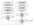
- FIG. 2illustrates a flow diagram of elements for an embodiment of a method to form a dielectric layer containing a nanolaminate layered sequence of cerium oxide (CeO 2 ) and aluminum oxide (Al 2 O 3 ) by atomic layer deposition, according to various embodiments;
- FIG. 3illustrates an embodiment of a configuration of a transistor having a dielectric layer containing an atomic layer deposited nanolaminate layered sequence of cerium oxide (CeO 2 ) and aluminum oxide (Al 2 O 3 ) dielectric layer;
- FIG. 4shows an embodiment of a configuration of a capacitor having a dielectric layer containing an atomic layer deposited nanolaminate layered sequence of cerium oxide (CeO 2 ) and aluminum oxide (Al 2 O 3 ) dielectric layer;
- FIG. 5is a simplified diagram for an embodiment of a controller coupled to an electronic device.
- FIG. 6illustrates a diagram for an embodiment of an electronic system having devices with a dielectric film containing an atomic layer deposited nanolaminate layered sequence of cerium oxide (CeO 2 ) and aluminum oxide (Al 2 O 3 ) dielectric layer.
- wafer and substrate used in the following descriptioninclude any structure having an exposed surface with which to form an integrated circuit (IC) structure.
- substrateis understood to include semiconductor wafers.
- substrateis also used to refer to semiconductor structures during processing, and may include other layers that have been fabricated thereupon. Both wafer and substrate include doped and undoped semiconductors, epitaxial semiconductor layers supported by a base semiconductor or insulator, as well as other semiconductor structures well known to one skilled in the art.
- conductoris understood to generally include n-type and p-type semiconductors and the term insulator or dielectric is defined to include any material that is less electrically conductive than the materials referred to as conductors or as semiconductors.
- horizontalas used in this application is defined as a plane parallel to the conventional plane or surface of a wafer or substrate, regardless of the orientation of the wafer or substrate.
- verticalrefers to a direction perpendicular to the horizontal as defined above. Prepositions, such as “on”, “side” (as in “sidewall”), “higher”, “lower”, “over” and “under” are defined with respect to the conventional plane or surface being on the top surface of the wafer or substrate, regardless of the orientation of the wafer or substrate.
- a gate dielectric in a transistorhas both a physical gate dielectric thickness and an equivalent oxide thickness (t eq ).
- the equivalent oxide thicknessquantifies the electrical properties, such as capacitance, of the gate dielectric in terms of a representative physical thickness.
- t eqis defined as the thickness of a theoretical SiO 2 layer that would be required to have the same capacitance density as a given dielectric, ignoring leakage current and reliability considerations.
- a SiO 2 layer of thickness, t, deposited on a Si surface as a gate dielectricwill have a t eq larger than its thickness, t.
- This t eqresults from the capacitance in the surface channel on which the SiO 2 is deposited due to the formation of a depletion/inversion region.
- This depletion/inversion regioncan result in t eq being from 3 to 6 Angstroms ( ⁇ ) larger than the SiO 2 thickness, t.
- the gate dielectric equivalent oxide thicknessto under 10 ⁇
- the physical thickness requirement for a SiO 2 layer used for a gate dielectricwould be need to be approximately 4 to 7 ⁇ .
- SiO 2 layerAdditional requirements on a SiO 2 layer would depend on the gate electrode used in conjunction with the SiO 2 gate dielectric. Using a conventional polysilicon gate would result in an additional increase in t eq for the SiO 2 layer. This additional thickness could be eliminated by using a metal gate electrode, though metal gates are not currently used in typical complementary metal-oxide-semiconductor field effect transistor (CMOS) technology. Thus, future devices may require a physical SiO 2 gate dielectric layer of about 5 A or less. Such a small thickness requirement for a SiO 2 oxide layer creates additional problems.
- CMOScomplementary metal-oxide-semiconductor field effect transistor
- Silicon dioxideis used as a gate dielectric, in part, due to its electrical isolation properties in a SiO 2 —Si based structure. This electrical isolation is due to the relatively large band gap of SiO 2 (8.9 eV) making it a good insulator from electrical conduction. Signification reductions in its band gap would eliminate SiO 2 as a material for a gate dielectric. As the thickness of a SiO 2 layer decreases, the number of atomic layers, or monolayers of the material in the thickness decreases. At a certain thickness, the number of monolayers will be sufficiently small that the SiO 2 layer will not have a complete arrangement of atoms as in a thicker or bulk layer.
- a thin SiO 2 layer of only one or two monolayerswill not form a full band gap.
- the lack of a full band gap in a SiO 2 gate dielectricmay cause an effective short between an underlying conductive silicon channel and an overlying polysilicon gate. This undesirable property sets a limit on the physical thickness to which a SiO 2 layer can be scaled. The minimum thickness due to this monolayer effect is thought to be about 7-8 ⁇ . Therefore, for future devices to have a t eq less than about 10 ⁇ , other dielectrics than SiO 2 need to be considered for use as a gate dielectric.
- materials with a dielectric constant greater than that of SiO 2will have a physical thickness that can be considerably larger than a desired t eq , while providing the desired equivalent oxide thickness.
- an alternate dielectric material with a dielectric constant of 10such as Al 2 O 3
- a reduced equivalent oxide thickness for transistorscan be realized by using dielectric materials with higher dielectric constants than SiO 2 .
- the thinner equivalent oxide thickness required for lower transistor operating voltages and smaller transistor dimensionsmay be realized by a significant number of materials, but additional fabricating requirements makes determining a suitable replacement for SiO 2 difficult.
- the current view for the future of the microelectronics industrystill predicts silicon based devices. This requires that the gate dielectric employed be grown on a silicon substrate or silicon layer, which places significant constraints on the substitute dielectric material. During the formation of the dielectric on the silicon layer, there exists the possibility that a small layer of SiO 2 could be formed in addition to the desired dielectric. The result would effectively be a dielectric layer consisting of two sub-layers in parallel with each other and the silicon layer on which the dielectric is formed.
- the resulting capacitancewould be that of two dielectrics in series.
- the t eqt SiO 2 +( ⁇ ox / ⁇ ) t.
- SiO 2as a gate dielectric
- Having an amorphous structure for a gate dielectricprovides reduced leakage current problems associated with grain boundaries in polycrystalline gate dielectrics, which may cause high leakage paths. Additionally, grain size and orientation changes throughout a polycrystalline gate dielectric can cause variations in the film's dielectric constant, along with uniformity and surface topography problems.
- materials having the advantage of a high dielectric constant relative to SiO 2also have the disadvantage of a crystalline form, at least in a bulk configuration.
- the best candidates for replacing SiO 2 as a gate dielectricare those with high dielectric constant, which can be fabricated as a thin layer with an amorphous form. Aluminum oxide alloyed with other oxides has been shown to raise the crystallization temperature of those oxides, and thus stabilize the long term interfacial characteristics of the amorphous dielectric.
- High- ⁇ materialsinclude materials having a dielectric constant greater than silicon dioxide, for example, dielectrics materials having a dielectric constant greater than about twice the dielectric constant of silicon dioxide.
- An appropriate high- ⁇ gate dielectricshould have a large energy gap (E g ) and large energy barrier heights with the silicon substrate for both electrons and holes.
- E genergy gap
- the band gapis inversely related to the dielectric constant for a high- ⁇ material, which lessens some advantages of the high- ⁇ material.
- a set of high- ⁇ dielectric candidates for replacing silicon oxide as the dielectric material in electronic components in integrated circuitsincludes the lanthanide oxides such as Ce 2 O 3 , La 2 O 3 , Pr 2 O 3 , Nd 2 O 3 , Sm 2 O 3 , Gd 2 O 3 , Dy 2 O 3 , Tb 2 O 3 , Er 2 O 3 , Eu 2 O 3 , Lu 2 O 3 , Tm 2 O 3 , Ho 2 O 3 , Pm 2 O 3 , and Yb 2 O 3 .
- Other candidatesinclude various lanthanide silicates and zirconium oxide, ZrO 2 .
- Such high dielectric constant layersprovide a significantly thinner equivalent oxide thickness compared with a silicon oxide layer having the same physical thickness. Alternately, such dielectric layers provide a significantly thicker physical thickness than a silicon oxide layer having the same equivalent oxide thickness. This increased physical thickness aids in reducing leakage current.
- Another consideration for selecting the material and method for forming a dielectric film for use in electronic devices and systemsconcerns the roughness of a dielectric film on a substrate. Surface roughness of the dielectric film has a significant effect on the electrical properties of the gate oxide, and the resulting operating characteristics of the transistor.
- the leakage current through a physical 1.0 nm gate dielectricmay increase by a factor of 10 for every 0.1 increase in the root-mean-square (RMS) roughness of the dielectric layer.
- RMSroot-mean-square
- a dielectric film having a substantially smooth surface relative to other processing techniquesis formed using atomic layer deposition (ALD). Further, forming such a dielectric film using atomic layer deposition can provide for controlling transitions between different material layers. As a result of such control, atomic layer deposited dielectric film may have an engineered transition with a substrate surface, or may be formed with many thin layers of different dielectric materials to enable selection of the dielectric constant to a value between that available from pure dielectric compounds.
- ALDatomic layer deposition
- ALDwhich may be known as atomic layer epitaxy (ALE), is a modification of chemical vapor deposition (CVD) and may also be called “alternatively pulsed-CVD.”
- ALEatomic layer epitaxy
- CVDchemical vapor deposition
- ALDgaseous precursors are introduced one at a time to the substrate surface mounted within a reaction chamber (or reactor). This introduction of the gaseous precursors takes the form of pulses of each gaseous precursor.
- the precursor gasis made to flow into a specific area or region for a short period of time.
- the reaction chamberis purged with a gas, which in many cases is an inert gas, and/or evacuated.
- the first precursorsaturates and is chemisorbed at the substrate surface process, during the first pulsing phase. Subsequent pulsing with a purging gas removes excess precursor from the reaction chamber, specifically the precursor that has not been chemisorbed.
- the second pulsing phaseintroduces a second precursor to the substrate where the growth reaction of the desired film takes place, with a reaction thickness that depends upon the amount of chemisorbed first precursor. Subsequent to the film growth reaction, reaction byproducts and precursor excess are purged from the reaction chamber. With a precursor chemistry where the precursors adsorb and react with each other on the substrate aggressively, one ALD cycle can be preformed in less than one second in properly designed flow type reaction chambers. Typically, precursor pulse times range from about 0.5 sec to about 2 to 3 seconds.
- ALDALD processes
- the saturation of all the reaction and purging phasesmakes the film growth self-limiting.
- This self-limiting growthresults in large area uniformity and conformality, which has important applications for such cases as planar substrates, deep trenches, and in the processing of porous silicon and high surface area silica and alumina powders.
- ALDprovides for controlling film thickness in a straightforward manner by controlling the number of growth cycles.
- ALDwas originally developed to manufacture luminescent and dielectric films needed in electroluminescent displays. Significant efforts have been made to apply ALD to the growth of doped zinc sulfide and alkaline earth metal sulfide films. Additionally, ALD has been studied for the growth of different epitaxial II-V and II-VI films, nonepitaxial crystalline or amorphous oxide and nitride films and multilayer structures of these. There also has been considerable interest towards the ALD growth of silicon and germanium films, but due to the difficult precursor chemistry, this has not been very successful.
- the precursors used in an ALD processmay be gaseous, liquid or solid. However, liquid or solid precursors should be volatile. The vapor pressure should be high enough for effective mass transportation. In addition, solid and some liquid precursors may need to be heated inside the reaction chamber and introduced through heated tubes to the substrates. The necessary vapor pressure should be reached at a temperature below the substrate temperature to avoid the condensation of the precursors on the substrate. Due to the self-limiting growth mechanisms of ALD, relatively low vapor pressure solid precursors can be used though evaporation rates may vary somewhat during the process because of changes in their surface area.
- precursors used in ALDthere are several other characteristics for precursors used in ALD.
- the precursorsshould be thermally stable at the substrate temperature because their decomposition would destroy the surface control and accordingly the advantages of the ALD method that relies on the reaction of the precursor at the substrate surface. A slight decomposition, if slow compared to the ALD growth, can be tolerated.
- the precursorsshould chemisorb on, or react with the surface, though the interaction between the precursor and the surface as well as the mechanism for the adsorption is different for different precursors.
- the molecules at the substrate surfaceshould react aggressively with the second precursor, which may be called a reactant, to form the desired solid film. Additionally, precursors should not react with the film to cause etching, and precursors should not dissolve in the film.
- the use of highly reactive precursors in ALDcontrasts with the selection of precursors for conventional CVD type reactions.
- the by-products in the reactionshould be gaseous in order to allow their easy removal from the reaction chamber during a purge stage. Further, the by-products should not react or adsorb on the surface.
- RS-ALDreaction sequence ALD
- the self-limiting process sequenceinvolves sequential surface chemical reactions.
- RS-ALDrelies on chemistry between a reactive surface and a reactive molecular precursor.
- molecular precursorsare pulsed into the ALD reaction chamber separately.
- the metal precursor reaction at the substrateis typically followed by an inert gas pulse (or purge) to remove excess precursor and by-products from the reaction chamber prior to an input pulse of the next precursor of the fabrication sequence.
- filmscan be layered in equal metered sequences that are all identical in chemical kinetics, deposition per cycle, composition, and thickness.
- RS-ALD sequencesgenerally deposit less than a full layer of the material being deposited per cycle, for example CeO 2 .
- a deposition rate of about 0.25 to about 2.00 ⁇ per RS-ALD cyclecan be realized.
- RS-ALDThe advantages of RS-ALD include continuity at an interface avoiding poorly defined nucleating regions that are typical for thin chemical vapor deposition ( ⁇ 20 ⁇ ) and physical vapor deposition ( ⁇ 50 ⁇ ), conformality over a variety of substrate topologies due to its layer-by-layer deposition technique, use of low temperature and mildly oxidizing processes, lack of dependence on the reaction chamber, growth thickness dependent solely on the number of cycles performed, and ability to engineer multilayer laminate films with resolution of one to two monolayers.
- RS-ALD processesallows for deposition control on the order of single monolayers and the ability to deposit monolayers of amorphous films.
- a cycle of a deposition sequenceincludes pulsing a precursor material, pulsing a purging gas for the precursor, pulsing a reactant precursor, and pulsing the reactant's purging gas, resulting in a very consistent deposition thickness that depends upon the amount of the first precursor that absorbs onto, and saturates, the surface.
- This cyclemay be repeated until the desired thickness is achieved in a single material dielectric layer, or may be alternated with pulsing a third precursor material, pulsing a purging gas for the third precursor, pulsing a fourth reactant precursor, and pulsing the fourth reactant's purging gas.
- a nanolaminatemeans a composite film of ultra thin layers of two or more different materials in a layered stack, where the layers are alternating layers of the different materials having a thickness on the order of a nanometer, and may be a continuous film only a single monolayer thick of the material.
- the nanolayersare not limited to alternating single layers of each material, but may include having several layers of one material alternating with a single layer of the other material, to obtain a desired ratio of the two or more materials. Such an arrangement may obtain a dielectric constant that is between the values of the two materials taken singly.
- the dielectric layermay be made of single layers of the two or more materials that are deposited individually, but may never the less be essentially a single film formed of an alloy between the two of more individual films. This may depend upon the particular materials being used and their physical and chemical properties relative to one another. If the materials are miscible the result is likely to be a single dielectric layer or alloy.
- a nanolaminate layer of cerium oxide and aluminum oxideis formed on a substrate mounted in a reaction chamber using RS-ALD in a repetitive sequence using precursor gases individually pulsed into the reaction chamber.
- An embodimentincludes forming the cerium oxide using a metal alkoxy complex precursor gas such as 1,10 phenanthroline tris 2,2,6,6 tetramethyl heptanedonadionato cerium, (Ce(thd) 3 phen).
- An embodimentincludes forming the aluminum oxide using a metal alkoxy complex precursor gas, such as trimethyl aluminum.
- Other solid or liquid precursorsmay be used in an appropriately designed reaction chamber.
- RS-ALD reaction chambermay result in lower deposition temperatures in the range of 300 degrees Celsius or lower, and the ability to use mildly oxidizing reactant materials such as H 2 O, H 2 O 2 , various alcohols, N 2 O, ozone or oxygen.
- Purge gasesmay include nitrogen, helium, argon or neon.
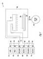
- FIG. 1shows an embodiment of an atomic layer deposition system 100 for forming a nanolaminate dielectric film containing cerium oxide alternating with aluminum oxide.
- a substrate 108 on a heating element/wafer holder 106is located inside a reaction chamber 102 of ALD system 100 .
- the heating element 106is thermally coupled to substrate 108 to control the substrate temperature.
- a gas-distribution fixture 110introduces precursor, reactant and purge gases to the substrate 108 in a uniform fashion.
- the gases introduced by the gas distribution fixturesometimes referred to a showerhead, react with the substrate 108 , and any excess gas and reaction products are removed from chamber 102 by vacuum pump 104 through a control valve 105 .
- Each gasoriginates from individual gas sources 114 , 118 , 122 , 126 , 130 , and 134 , with a flow rate and time controlled by mass-flow controllers 116 , 120 , 124 , 128 , 132 and 136 , respectively.
- Gas sources 122 and 130provide a precursor gas either by storing the precursor as a gas or by providing a location and apparatus for evaporating a solid or liquid material to form the selected precursor gas.
- purging gas sources 114 and 118are also included in the system.
- the embodimentmay use only one of the purge gases for all four disclosed illustrative purging steps, or both purge gases may be used simultaneously, or alternately as required for the particular desired result.
- additional purging gas sourcescan be constructed in ALD system 100 , one purging gas source for each different precursor and reactant gas, for example. For a process that uses the same purging gas for multiple precursor gases less purging gas sources may be required for ALD system 100 .
- the precursor, reactant and purge gas sourcesare coupled by their associated mass-flow controllers to a common gas line or conduit 112 , which is coupled to the gas-distribution fixture 110 inside the reaction chamber 102 .
- Gas conduit 112may also be coupled to another vacuum pump, or exhaust pump, not shown, to remove excess precursor gases, purging gases, and by-product gases at the end of a purging sequence from the gas conduit 112 .
- Vacuum pump, or exhaust pump, 104is coupled to chamber 102 by control valve 105 , which may be a mass-flow valve, to remove excess precursor gases, purging gases, and by-product gases from reaction chamber 102 at the end of a purging sequence.
- control valve 105may be a mass-flow valve, to remove excess precursor gases, purging gases, and by-product gases from reaction chamber 102 at the end of a purging sequence.
- control displays, mounting apparatus, temperature sensing devices, substrate maneuvering apparatus, and necessary electrical connections as are known to those skilled in the artare not shown in FIG. 1 .
- ALD system 100is well suited for depositing CeO 2 /Al 2 O 3 films, other ALD systems commercially available may also be used.
- reaction chambersfor deposition of films are understood by those of ordinary skill in the art of semiconductor fabrication. A variety of such reaction chambers may be used. Furthermore, one of ordinary skill in the art will comprehend the necessary detection, measurement, and control techniques in the art of semiconductor fabrication upon reading and understanding the disclosure.
- ALD system 100may be controlled by a computer. To focus on the use of ALD system 100 , the computer is not shown. Those skilled in the art can appreciate that the individual elements such as pressure control, temperature control, and gas flow within ALD system 100 can be under computer control.
- FIG. 2illustrates a flow diagram of operational steps for an embodiment of a method to form a nanolaminate dielectric layer containing a cerium oxide alternating with aluminum oxide layer.
- a substrateis prepared to react immediately with, and chemisorb the first precursor gas. This preparation will remove contaminants such as thin organic films, dirt, and native oxide from the surface of the substrate, and may include a hydrofluoric acid rinse, or a sputter etch in the reaction chamber 102 .
- a first precursor materialenters the reaction chamber for a predetermined length of time, in an embodiment 0.5-2.0 seconds.
- An embodimentincludes the first precursor material being a metal alkoxy complex precursor gas, but other cerium containing gases, liquids and sublimating solids may also be used.
- the first precursor materialis chemically absorbed onto the surface of the substrate, the amount depending upon the temperature of the substrate, in one embodiment 300 degrees C., and the presence of sufficient flow of the precursor material.
- the pulsing of the precursormay use a pulsing period that provides uniform coverage of an absorbed monolayer on the substrate surface, or may use a pulsing period that provides partial formation of a monolayer on the substrate surface.
- a first purge gasenters the reaction chamber for a predetermined length of time sufficient to remove substantially all of the non-chemisorbed first precursor material. Typical times may be 1.0-2.0 seconds with a purge gas comprising nitrogen, argon, neon, combinations thereof or other gases such as hydrogen.
- a first reactant gasenters the chamber for a predetermined length of time, sufficient to provide enough of the reactant to chemically combine with the amount of chemisorbed first precursor material on the surface of the substrate. Typical reactant materials include mildly oxidizing materials, including but not limited to water vapor, hydrogen peroxide, nitrogen oxides, ozone and oxygen gas, and combinations thereof.
- a second purge gaswhich may be the same or different from the first purge gas, enters the chamber for a predetermined length of time, sufficient to remove substantially all non reacted materials and any reaction byproducts from the chamber.
- a second precursor materialenters the reaction chamber for a predetermined length of time, for example 0.5-2.0 seconds.
- An embodimentincludes the first precursor material being a metal alkoxy complex precursor gas such as trimethyl aluminum, but other aluminum containing materials, in gas, liquid or sublimating solid form, may also be used.
- the second precursor materialis chemically absorbed onto the surface of the substrate, in this case being the top surface of the first dielectric material, the amount of absorption depending upon the temperature of the substrate, in one embodiment 300 degrees C., and the presence of sufficient flow of the precursor material.
- the pulsing of the precursormay use a pulsing period that provides uniform coverage of an absorbed monolayer on the substrate surface, or may use a pulsing period that provides partial formation of a monolayer on the substrate surface.
- the first purge gasis shown as entering the chamber, but the invention is not so limited.
- the purge gas used in the second dielectric material depositionmay be the same or different from either of the two previously noted purge gases, and FIG. 1 could be shown as having more than the two purge gases shown.
- the purge cyclecontinues for a predetermined length of time sufficient to remove substantially all of the non-chemisorbed second precursor material.
- a second reactant gaswhich may the same or different from the first reactant gas, enters the chamber for a predetermined length of time, sufficient to provide enough of the reactant to chemically combine with the amount of chemisorbed second precursor material on the surface of the substrate.
- another purge gasenters the chamber, which may be the same or different from any of the three previously discussed purge gases, for a predetermined length of time, sufficient to remove substantially all non reacted materials and any reaction byproducts from the chamber.
- the desired thicknesses of the first and second dielectric materials in the nanolaminate dielectricmay not be the same thickness, and there may be more deposition cycles for one dielectric material as compared to the other. For example, in one embodiment the number of cerium oxide layers is two for each one layer of aluminum oxide. If the second dielectric layer has reached the desired thickness the process moves on to a decision at 224 of whether the number of layers of the first and second dielectric materials has reached the desired number.
- a single layer of the first dielectric and a single layer of the second dielectrichave been completed at this point in the process. If more than a single layer of each dielectric material is desired the process moves back to another deposition of the first dielectric material at 206 . After the number of interleaved layers of dielectrics one and two has reached the desired value, the deposition ends at 226 .
- the present illustrative embodimentdiscusses and illustrates that the layers are distinct from each other, the individual layers are very thin and may act effectively as a single alloy layer.
- the embodiments described hereinprovide a process for growing a dielectric film having a wide range of useful equivalent oxide thickness, t eq , associated with a dielectric constant in the range from about 10 to about 30.
- This range of dielectric constantsprovides for a t eq ranging from about 13% to about 36% relative to a given silicon dioxide thickness.
- an embodiment for a cerium oxidemay have a physical oxide thickness from three to eight times larger than the acceptable silicon dioxide thickness, providing reduced leakage current due to the thicker dielectric layer.
- dielectric films of cerium oxide formed by atomic layer depositioncan provide not only equivalent thin t eq films, but also films with relatively low leakage current.
- novel processcan be implemented to form transistors, capacitors, memory devices, and other electronic systems including information handling devices.
- the present subject matteris not limited to two dielectric materials (that is, a binary dielectric), and the equipment described in FIG. 1 could have included a precursor and reactant 3,4, which are not described for simplicity.
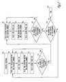
- FIG. 3illustrates a single transistor in an embodiment of a method to form a dielectric layer containing an RS-ALD deposited cerium oxide/aluminum oxide gate oxide layer.
- a substrate 302is prepared, typically a silicon or silicon containing material. In other embodiments, germanium, gallium arsenide, silicon-on-sapphire substrates, or other suitable substrates may also be used.
- This preparation processincludes cleaning substrate 302 and forming various layers and regions of the substrate, such as drain diffusion 304 and source diffusion 306 of an illustrative metal oxide semiconductor (MOS) transistor 300 , prior to forming a gate dielectric.
- MOSmetal oxide semiconductor
- the substrateis typically cleaned to provide an initial substrate depleted of its native oxide.
- the substratemay also be cleaned to provide a hydrogen-terminated surface.
- a silicon substratemay undergo a final hydrofluoric (HF) rinse prior to ALD processing to provide the silicon substrate with a hydrogen-terminated surface without a native silicon oxide layer.
- Cleaning immediately preceding atomic layer depositionaids in reducing an occurrence of silicon oxide as an interface between silicon based substrate and dielectric formed using the atomic layer deposition process.
- the sequencing of the formation of the regions of the transistor being processedmay follow typical sequencing that is generally performed in the fabrication of a MOS transistor as is well known to those skilled in the art.
- the dielectric covering the area on the substrate 302 between the source and drain diffused regions 304 and 306is deposited by RS-ALD in this illustrative embodiment, and comprises cerium oxide layers 308 , 310 , and 314 , having interleaved aluminum oxide layers, 312 and 316 .
- This alloy dielectric layermay be referred to as the gate oxide.
- the cerium oxide layer 308is shown as being the first layer and in direct contact with the substrate 302 ; the present subject matter, however, is not so limited. There may be a diffusion barrier layer inserted between the first dielectric layer 308 and the substrate 302 to prevent metal contamination from affecting the electrical properties of the device.
- the described embodimentmay also include having the first dielectric layer as aluminum oxide, since this affects the surface states and the work function of the dielectric layer.
- the illustrative embodimentalso shows the different dielectric layers having the same thickness; however, the desired dielectric properties of the nanolaminate film may be best achieved by adjusting the ratio of the thickness of the two dielectric materials to different values.
- the ratio between the total thickness of cerium oxide layers 308 , 310 and 314is twice the total thickness of the aluminum oxide layers 312 and 316 .
- the transistor 300has a conductive material forming a gate 318 in this illustrative embodiment, but the nanolaminate dielectric may also be used in a floating gate device such as an EEPROM transistor, as both the floating gate and the control gate oxide layers.
- the gate dielectric(layers 308 - 316 ) forms a tunnel gate insulator and a floating gate dielectric in a flash memory device.
- Use of dielectric layers containing a nanolaminate atomic layer deposited dielectric layer for a gate dielectric and/or floating gate dielectric in which the dielectric layer contacts a conductive layeris not limited to silicon based substrates, but may be used with a variety of semiconductor substrates.
- a methodincludes forming a first conductive layer 402 , a second conductive layer 404 , and a nanolaminate dielectric having interleaved layers 406 - 416 of two or more different dielectric materials formed between the two conductive layers.
- the conductive layers 402 and 404may be formed of metals, doped polysilicon, silicided metals, polycides, or conductive organic compounds. The sequencing of the layers depends on the application.
- the effective dielectric constant associated with a nanolaminate structureis attributable to N capacitors in series, where each capacitor has a thickness defined by the thickness of the corresponding layer.
- a nanolaminate structurecan be engineered to have a predetermined dielectric constant.
- Structures such as the nanolaminate structure shown in FIGS. 3 and 4may be used in NROM flash memory devices as well as other integrated circuits.
- Transistors, capacitors, and other devices having dielectric filmsmay be implemented into memory devices and electronic systems including information handling devices. Embodiments of these information handling devices may include wireless systems, telecommunication systems, computers and integrated circuits.
- FIG. 5illustrates a diagram for an electronic system 500 having one or more devices having a dielectric layer containing an atomic layer deposited oxide layer formed according to various embodiments.
- Electronic system 500includes a controller 502 , a bus 504 , and an electronic device 506 , where bus 504 provides electrical conductivity between controller 502 and electronic device 506 .
- controller 502 and/or electronic device 506includes an embodiment for a dielectric layer containing a nanolaminate RS-ALD deposited oxide layer as previously discussed.
- Electronic system 500may include, but is not limited to, information handling devices, wireless systems, telecommunication systems, fiber optic systems, electro-optic systems, and computers.
- FIG. 6depicts a diagram of an embodiment of a system 600 having a controller 602 and a memory 606 .
- Controller 602 and/or memory 606may include a dielectric layer having a nanolaminate RS-ALD dielectric layer.
- System 600also may include an electronic apparatus 608 , and a bus 604 , where bus 604 may provide electrical conductivity and data transmission between controller 602 and electronic apparatus 608 , and between controller 602 and memory 606 .
- Bus 604may include an address, a data bus, and a control bus, each independently configured. Bus 604 may also use common conductive lines for providing address, data, and/or control, the use of which may be regulated by controller 602 .
- electronic apparatus 608may include additional memory devices configured similarly to memory 606 .
- An embodimentmay include an additional peripheral device or devices 610 coupled to bus 604 .
- controller 602is a processor. Any of controller 602 , memory 606 , bus 604 , electronic apparatus 608 , and peripheral device devices 610 may include a dielectric layer having a nanolaminate RS-ALD deposited oxide layer in accordance with the disclosed embodiments.
- System 600may include, but is not limited to, information handling devices, telecommunication systems, and computers.
- Peripheral devices 610may include displays, additional storage memory, or other control devices that may operate in conjunction with controller 602 and/or memory 606 . It will be understood that embodiments are equally applicable to any size and type of memory circuit and are not intended to be limited to a particular type of memory device.
- Memory typesinclude a DRAM, SRAM (Static Random Access Memory) or Flash memories.
- the DRAMcould be a synchronous DRAM commonly referred to as SGRAM (Synchronous Graphics Random Access Memory), SDRAM (Synchronous Dynamic Random Access Memory), SDRAM II, and DDR SDRAM (Double Data Rate SDRAM), as well as Synchlink or Rambus DRAMs and other emerging DRAM technologies.
- SGRAMSynchronous Graphics Random Access Memory
- SDRAMSynchronous Dynamic Random Access Memory
- SDRAM IISynchroble Data Rate SDRAM
- DDR SDRAMDouble Data Rate SDRAM
- cerium oxide/aluminum oxide layers by a RS-ALD depositionmay be realized using a trimethyl aluminum precursor and a cerium methyl alkoxy precursor. These dielectric films formed by RS-ALD and processed in relatively low temperatures, such as 300 degrees Celsius, may be amorphous and possess smooth surfaces. Such RS-ALD oxide films may provide enhanced electrical properties as compared to physical deposition methods, such as sputtering or typical chemical layer depositions, due to their smoother surface, and reduced damage, resulting in reduced leakage current. In particular the alloy of aluminum oxide improves the ability of cerium oxide films to remain in an amorphous state, and improves the thermal stability and interface properties of the resultant dielectric film. Amounts of aluminum oxide ranging from 10% to 45% of the total film composition are useful gate dielectrics.
- dielectric layershave adjustable dielectric constants that are higher than the commonly used silicon dioxide and silicon nitride based dielectrics, and provide a significantly thicker physical thickness than a silicon oxide layer having the same equivalent oxide thickness, where the increased thickness may also reduce leakage current issues, and reduce oxide shorts due to pinholes and reduced thickness areas.
- Capacitors, transistors, higher level ICs or devices including memory devices, and electronic systemsare constructed utilizing the novel process for forming a dielectric film having an ultra thin equivalent oxide thickness, t eq .
- Gate dielectric layers or films containing atomic layer deposited lanthanide oxideare formed having a dielectric constant ( ⁇ ) substantially higher than that of silicon oxide, such that these dielectric films are capable of a t eq thinner than SiO 2 gate dielectrics of the same physical thickness.
- the high dielectric constant relative to silicon dioxideallows the use of much larger physical thickness of these high- ⁇ dielectric materials for the same t eq of SiO 2 . Forming the relatively larger thickness aids in processing gate dielectrics and other dielectric layers in electronic devices and systems.
- An embodiment of a method for forming an electronic deviceincludes forming a dielectric layer by using an atomic layer deposition (ALD) technique to form a nanolaminate layered dielectric having alternating layers of cerium oxide (CeO 2 ) and aluminum oxide (Al 2 O 3 ).
- ALDatomic layer deposition
- the inventionis not limited as to which layer is deposited first, and the resulting dielectric structure acts as a single dielectric layer.
- An embodiment of the structureis formed by depositing cerium oxide by atomic layer deposition onto a substrate surface using precursor chemicals containing cerium compounds, followed by a purge and deposition of an oxidizing material such as water vapor to form a thin (often a single molecular layer) film of CeO 2 , then ALD depositing aluminum onto the substrate using precursor chemicals containing aluminum compounds, followed by a purge and deposition of an oxidizing material such as water vapor to form a thin (often a single molecular layer) film of Al 2 O 3 , and repeating as often as appropriate to form a thin laminate dielectric structure of the desired thickness.
- a dielectric layer formed of cerium oxide and aluminum oxidemay be beneficially used in electronic devices because the high dielectric constant (high-k) of the film provides the functionality of a much thinner silicon dioxide film without the reliability loss consequent to using such physically thin films.
- Embodimentsinclude structures for capacitors, transistors, memory devices, and electronic systems with dielectric layers containing an atomic layer deposited cerium oxide and aluminum oxide, and methods for forming such structures.
Landscapes
- Chemical & Material Sciences (AREA)
- Engineering & Computer Science (AREA)
- Chemical Kinetics & Catalysis (AREA)
- General Chemical & Material Sciences (AREA)
- Manufacturing & Machinery (AREA)
- Condensed Matter Physics & Semiconductors (AREA)
- Microelectronics & Electronic Packaging (AREA)
- Power Engineering (AREA)
- Physics & Mathematics (AREA)
- Organic Chemistry (AREA)
- General Physics & Mathematics (AREA)
- Computer Hardware Design (AREA)
- Materials Engineering (AREA)
- Mechanical Engineering (AREA)
- Metallurgy (AREA)
- Inorganic Chemistry (AREA)
- Crystallography & Structural Chemistry (AREA)
- Formation Of Insulating Films (AREA)
- Semiconductor Memories (AREA)
Abstract
Description
- This application is a divisional of U.S. application Ser. No. 11/055,380, filed Feb. 10, 2005, which is incorporated herein by reference.
- This application relates generally to semiconductor devices and device fabrication and, more particularly, to dielectric layers and their method of fabrication.
- The semiconductor device industry has a market driven need to reduce the size of devices such as transistors in order to obtain lower power consumption and higher performance. To reduce transistor size, the thickness of the silicon dioxide, SiO2, gate dielectric is reduced in proportion to the shrinkage of the gate length. For example, a metal-oxide-semiconductor field effect transistor (MOSFET) would use a 1.5 nm thick SiO2gate dielectric for a gate length of 70 nm. A goal is to fabricate increasingly smaller and more reliable integrated circuits (ICs) for use in products such as processor chips, mobile telephones, and memory devices such as dynamic random access memories (DRAMs).
- Currently, the semiconductor industry relies on the ability to reduce or scale the dimensions of its basic devices, such as the silicon based MOSFET. This device scaling includes scaling the gate dielectric, which has been fabricated using silicon dioxide. A thermally grown amorphous SiO2layer provides an electrically and thermodynamically stable material, where the interface of the SiO2layer with underlying silicon provides a high quality interface as well as superior electrical isolation properties. However, increased scaling and other requirements in microelectronic devices have created the need to use other dielectric materials as gate dielectrics, in particular dielectrics with higher dielectric constants (k) to replace the conventional use of various combinations of SiO2, Si3N4and SiON. Practical higher dielectric constant (k) materials have the properties of high permittivity, thermal stability, high film and surface quality and smoothness, low hysteresis characteristics, low leakage current density, and long term reliability. High k films may be amorphous metal oxide unary materials such as Al2O3, CeO2, HfO2and ZrO2, which have a single component, or binary systems such as (Y2O3)X(ZrO2)1-X, LaAlO3, and (HfO2)X(Al2O3)1-X, which have two components, and so on. High k films may be single layers, or formed of multiple layers of different materials that act as a composite material. There is a need in the industry to find a method of forming high k films that possess the above noted features and are practical for use in manufacturing integrated circuits (ICs).
FIG. 1 depicts an atomic layer deposition system for fabricating a single dielectric layer formed as a nanolaminate layered sequence of cerium oxide (CeO2) and aluminum oxide (Al2O3), according to various embodiments of the present invention;FIG. 2 illustrates a flow diagram of elements for an embodiment of a method to form a dielectric layer containing a nanolaminate layered sequence of cerium oxide (CeO2) and aluminum oxide (Al2O3) by atomic layer deposition, according to various embodiments;FIG. 3 illustrates an embodiment of a configuration of a transistor having a dielectric layer containing an atomic layer deposited nanolaminate layered sequence of cerium oxide (CeO2) and aluminum oxide (Al2O3) dielectric layer;FIG. 4 shows an embodiment of a configuration of a capacitor having a dielectric layer containing an atomic layer deposited nanolaminate layered sequence of cerium oxide (CeO2) and aluminum oxide (Al2O3) dielectric layer;FIG. 5 is a simplified diagram for an embodiment of a controller coupled to an electronic device; andFIG. 6 illustrates a diagram for an embodiment of an electronic system having devices with a dielectric film containing an atomic layer deposited nanolaminate layered sequence of cerium oxide (CeO2) and aluminum oxide (Al2O3) dielectric layer.- The following detailed description refers to the accompanying drawings that show, by way of illustration, specific aspects and embodiments in which the present invention may be practiced. These embodiments are described in sufficient detail to enable those skilled in the art to practice the present invention. Other embodiments may be utilized and structural, logical, and electrical changes may be made without departing from the scope of the present invention. The various embodiments are not necessarily mutually exclusive, as some embodiments can be combined with one or more other embodiments to form new embodiments.
- The terms wafer and substrate used in the following description include any structure having an exposed surface with which to form an integrated circuit (IC) structure. The term substrate is understood to include semiconductor wafers. The term substrate is also used to refer to semiconductor structures during processing, and may include other layers that have been fabricated thereupon. Both wafer and substrate include doped and undoped semiconductors, epitaxial semiconductor layers supported by a base semiconductor or insulator, as well as other semiconductor structures well known to one skilled in the art. The term conductor is understood to generally include n-type and p-type semiconductors and the term insulator or dielectric is defined to include any material that is less electrically conductive than the materials referred to as conductors or as semiconductors.
- The term “horizontal” as used in this application is defined as a plane parallel to the conventional plane or surface of a wafer or substrate, regardless of the orientation of the wafer or substrate. The term “vertical” refers to a direction perpendicular to the horizontal as defined above. Prepositions, such as “on”, “side” (as in “sidewall”), “higher”, “lower”, “over” and “under” are defined with respect to the conventional plane or surface being on the top surface of the wafer or substrate, regardless of the orientation of the wafer or substrate. The following detailed description is, therefore, not to be taken in a limiting sense, and the scope of the present invention is defined only by the appended claims, along with the full scope of equivalents to which such claims are entitled.
- A gate dielectric in a transistor has both a physical gate dielectric thickness and an equivalent oxide thickness (teq). The equivalent oxide thickness quantifies the electrical properties, such as capacitance, of the gate dielectric in terms of a representative physical thickness. teqis defined as the thickness of a theoretical SiO2layer that would be required to have the same capacitance density as a given dielectric, ignoring leakage current and reliability considerations.
- A SiO2layer of thickness, t, deposited on a Si surface as a gate dielectric will have a teqlarger than its thickness, t. This teqresults from the capacitance in the surface channel on which the SiO2is deposited due to the formation of a depletion/inversion region. This depletion/inversion region can result in teqbeing from 3 to 6 Angstroms (Å) larger than the SiO2thickness, t. Thus, with the semiconductor industry driving to someday scale the gate dielectric equivalent oxide thickness to under 10 Å, the physical thickness requirement for a SiO2layer used for a gate dielectric would be need to be approximately 4 to 7 Å.
- Additional requirements on a SiO2layer would depend on the gate electrode used in conjunction with the SiO2gate dielectric. Using a conventional polysilicon gate would result in an additional increase in teqfor the SiO2layer. This additional thickness could be eliminated by using a metal gate electrode, though metal gates are not currently used in typical complementary metal-oxide-semiconductor field effect transistor (CMOS) technology. Thus, future devices may require a physical SiO2gate dielectric layer of about5 A or less. Such a small thickness requirement for a SiO2oxide layer creates additional problems.
- Silicon dioxide is used as a gate dielectric, in part, due to its electrical isolation properties in a SiO2—Si based structure. This electrical isolation is due to the relatively large band gap of SiO2(8.9 eV) making it a good insulator from electrical conduction. Signification reductions in its band gap would eliminate SiO2as a material for a gate dielectric. As the thickness of a SiO2layer decreases, the number of atomic layers, or monolayers of the material in the thickness decreases. At a certain thickness, the number of monolayers will be sufficiently small that the SiO2layer will not have a complete arrangement of atoms as in a thicker or bulk layer. As a result of incomplete formation relative to a bulk structure, a thin SiO2layer of only one or two monolayers will not form a full band gap. The lack of a full band gap in a SiO2gate dielectric may cause an effective short between an underlying conductive silicon channel and an overlying polysilicon gate. This undesirable property sets a limit on the physical thickness to which a SiO2layer can be scaled. The minimum thickness due to this monolayer effect is thought to be about 7-8 Å. Therefore, for future devices to have a teqless than about 10 Å, other dielectrics than SiO2need to be considered for use as a gate dielectric.
- For a typical dielectric layer used as a gate dielectric, the capacitance is determined as in a parallel plate capacitance: C=κε0A/t, where κ is the dielectric constant, ε0is the permittivity of free space, A is the area of the capacitor, and t is the thickness of the dielectric. The thickness, t, of a material is related to its teqfor a given capacitance, with SiO2having a dielectric constant Kox=3.9, as
t=(κ/κox)teq=(κ/3.9)teq.
Thus, materials with a dielectric constant greater than that of SiO2, (typically about 3.9), will have a physical thickness that can be considerably larger than a desired teq, while providing the desired equivalent oxide thickness. For example, an alternate dielectric material with a dielectric constant of 10, such as Al2O3, could have a thickness of about 25.6 Å to provide a teqof 10 Å, not including any depletion or inversion layer effects. Thus, a reduced equivalent oxide thickness for transistors can be realized by using dielectric materials with higher dielectric constants than SiO2. - The thinner equivalent oxide thickness required for lower transistor operating voltages and smaller transistor dimensions may be realized by a significant number of materials, but additional fabricating requirements makes determining a suitable replacement for SiO2difficult. The current view for the future of the microelectronics industry still predicts silicon based devices. This requires that the gate dielectric employed be grown on a silicon substrate or silicon layer, which places significant constraints on the substitute dielectric material. During the formation of the dielectric on the silicon layer, there exists the possibility that a small layer of SiO2could be formed in addition to the desired dielectric. The result would effectively be a dielectric layer consisting of two sub-layers in parallel with each other and the silicon layer on which the dielectric is formed. In such a case, the resulting capacitance would be that of two dielectrics in series. As a result, the teqof the dielectric layer would be the sum of the SiO2thickness and a multiplicative factor of the thickness, t, of the dielectric being formed, written as
teq=tSiO2 +(κox/κ)t.
Thus, if a SiO2layer is formed in the process, the teqis again limited by a SiO2layer. In the event that a barrier layer is formed between the silicon layer and the desired dielectric in which the barrier layer prevents the formation of a SiO2layer, the teqwould be limited by the layer with the lowest dielectric constant. However, whether a single dielectric layer with a high dielectric constant or a barrier layer with a higher dielectric constant than SiO2is employed, the layer directly in contact, or interfacing with the silicon layer must provide a high quality interface to maintain high channel carrier mobility. - One of the advantages of using SiO2as a gate dielectric has been that the formation of the SiO2layer results in an amorphous gate dielectric. Having an amorphous structure for a gate dielectric provides reduced leakage current problems associated with grain boundaries in polycrystalline gate dielectrics, which may cause high leakage paths. Additionally, grain size and orientation changes throughout a polycrystalline gate dielectric can cause variations in the film's dielectric constant, along with uniformity and surface topography problems. Typically, materials having the advantage of a high dielectric constant relative to SiO2also have the disadvantage of a crystalline form, at least in a bulk configuration. The best candidates for replacing SiO2as a gate dielectric are those with high dielectric constant, which can be fabricated as a thin layer with an amorphous form. Aluminum oxide alloyed with other oxides has been shown to raise the crystallization temperature of those oxides, and thus stabilize the long term interfacial characteristics of the amorphous dielectric.
- Candidates to replace SiO2include high-κ dielectric materials. High-κ materials include materials having a dielectric constant greater than silicon dioxide, for example, dielectrics materials having a dielectric constant greater than about twice the dielectric constant of silicon dioxide. An appropriate high-κ gate dielectric should have a large energy gap (Eg) and large energy barrier heights with the silicon substrate for both electrons and holes. Generally, the band gap is inversely related to the dielectric constant for a high-κ material, which lessens some advantages of the high-κ material. An example of a medium dielectric constant material (k=10) such as aluminum oxide, has a large bandgap of about 9 electron volts (eV). A set of high-κ dielectric candidates for replacing silicon oxide as the dielectric material in electronic components in integrated circuits includes the lanthanide oxides such as Ce2O3, La2O3, Pr2O3, Nd2O3, Sm2O3, Gd2O3, Dy2O3, Tb2O3, Er2O3, Eu2O3, Lu2O3, Tm2O3, Ho2O3, Pm2O3, and Yb2O3. Other candidates include various lanthanide silicates and zirconium oxide, ZrO2. Such high dielectric constant layers provide a significantly thinner equivalent oxide thickness compared with a silicon oxide layer having the same physical thickness. Alternately, such dielectric layers provide a significantly thicker physical thickness than a silicon oxide layer having the same equivalent oxide thickness. This increased physical thickness aids in reducing leakage current.
- Another consideration for selecting the material and method for forming a dielectric film for use in electronic devices and systems concerns the roughness of a dielectric film on a substrate. Surface roughness of the dielectric film has a significant effect on the electrical properties of the gate oxide, and the resulting operating characteristics of the transistor. The leakage current through a physical 1.0 nm gate dielectric may increase by a factor of 10 for every 0.1 increase in the root-mean-square (RMS) roughness of the dielectric layer.
- During a conventional sputtering deposition process, particles of the material to be deposited bombard the surface at a high energy. When a particle hits the surface, some particles adhere, and other particles cause damage. High energy impacts remove body region particles creating pits. The surface of such a deposited layer may have a rough contour due to the rough interface at the body region, and thus the electrical properties of a thin film may not be as good as the values in a bulk sample of the same material. Thus the method with which the thin film dielectric is deposited may have a substantial impact on the usefulness of the material in electronic devices.
- In an embodiment, a dielectric film having a substantially smooth surface relative to other processing techniques is formed using atomic layer deposition (ALD). Further, forming such a dielectric film using atomic layer deposition can provide for controlling transitions between different material layers. As a result of such control, atomic layer deposited dielectric film may have an engineered transition with a substrate surface, or may be formed with many thin layers of different dielectric materials to enable selection of the dielectric constant to a value between that available from pure dielectric compounds.
- ALD, which may be known as atomic layer epitaxy (ALE), is a modification of chemical vapor deposition (CVD) and may also be called “alternatively pulsed-CVD.” In ALD, gaseous precursors are introduced one at a time to the substrate surface mounted within a reaction chamber (or reactor). This introduction of the gaseous precursors takes the form of pulses of each gaseous precursor. In a pulse of a precursor gas, the precursor gas is made to flow into a specific area or region for a short period of time. Between the pulses, the reaction chamber is purged with a gas, which in many cases is an inert gas, and/or evacuated.
- In the first reaction step of the ALD process the first precursor saturates and is chemisorbed at the substrate surface process, during the first pulsing phase. Subsequent pulsing with a purging gas removes excess precursor from the reaction chamber, specifically the precursor that has not been chemisorbed.
- The second pulsing phase introduces a second precursor to the substrate where the growth reaction of the desired film takes place, with a reaction thickness that depends upon the amount of chemisorbed first precursor. Subsequent to the film growth reaction, reaction byproducts and precursor excess are purged from the reaction chamber. With a precursor chemistry where the precursors adsorb and react with each other on the substrate aggressively, one ALD cycle can be preformed in less than one second in properly designed flow type reaction chambers. Typically, precursor pulse times range from about 0.5 sec to about 2 to 3 seconds.
- In ALD processes, the saturation of all the reaction and purging phases makes the film growth self-limiting. This self-limiting growth results in large area uniformity and conformality, which has important applications for such cases as planar substrates, deep trenches, and in the processing of porous silicon and high surface area silica and alumina powders. Significantly, ALD provides for controlling film thickness in a straightforward manner by controlling the number of growth cycles.
- ALD was originally developed to manufacture luminescent and dielectric films needed in electroluminescent displays. Significant efforts have been made to apply ALD to the growth of doped zinc sulfide and alkaline earth metal sulfide films. Additionally, ALD has been studied for the growth of different epitaxial II-V and II-VI films, nonepitaxial crystalline or amorphous oxide and nitride films and multilayer structures of these. There also has been considerable interest towards the ALD growth of silicon and germanium films, but due to the difficult precursor chemistry, this has not been very successful.
- The precursors used in an ALD process may be gaseous, liquid or solid. However, liquid or solid precursors should be volatile. The vapor pressure should be high enough for effective mass transportation. In addition, solid and some liquid precursors may need to be heated inside the reaction chamber and introduced through heated tubes to the substrates. The necessary vapor pressure should be reached at a temperature below the substrate temperature to avoid the condensation of the precursors on the substrate. Due to the self-limiting growth mechanisms of ALD, relatively low vapor pressure solid precursors can be used though evaporation rates may vary somewhat during the process because of changes in their surface area.
- There are several other characteristics for precursors used in ALD. The precursors should be thermally stable at the substrate temperature because their decomposition would destroy the surface control and accordingly the advantages of the ALD method that relies on the reaction of the precursor at the substrate surface. A slight decomposition, if slow compared to the ALD growth, can be tolerated.
- The precursors should chemisorb on, or react with the surface, though the interaction between the precursor and the surface as well as the mechanism for the adsorption is different for different precursors. The molecules at the substrate surface should react aggressively with the second precursor, which may be called a reactant, to form the desired solid film. Additionally, precursors should not react with the film to cause etching, and precursors should not dissolve in the film. The use of highly reactive precursors in ALD contrasts with the selection of precursors for conventional CVD type reactions.
- The by-products in the reaction should be gaseous in order to allow their easy removal from the reaction chamber during a purge stage. Further, the by-products should not react or adsorb on the surface.
- In a reaction sequence ALD (RS-ALD) process, the self-limiting process sequence involves sequential surface chemical reactions. RS-ALD relies on chemistry between a reactive surface and a reactive molecular precursor. In an RS-ALD process, molecular precursors are pulsed into the ALD reaction chamber separately. The metal precursor reaction at the substrate is typically followed by an inert gas pulse (or purge) to remove excess precursor and by-products from the reaction chamber prior to an input pulse of the next precursor of the fabrication sequence.
- By the use of RS-ALD processes, films can be layered in equal metered sequences that are all identical in chemical kinetics, deposition per cycle, composition, and thickness. RS-ALD sequences generally deposit less than a full layer of the material being deposited per cycle, for example CeO2. Typically, a deposition rate of about 0.25 to about 2.00 Å per RS-ALD cycle can be realized.
- The advantages of RS-ALD include continuity at an interface avoiding poorly defined nucleating regions that are typical for thin chemical vapor deposition (<20 Å) and physical vapor deposition (<50 Å), conformality over a variety of substrate topologies due to its layer-by-layer deposition technique, use of low temperature and mildly oxidizing processes, lack of dependence on the reaction chamber, growth thickness dependent solely on the number of cycles performed, and ability to engineer multilayer laminate films with resolution of one to two monolayers. RS-ALD processes allows for deposition control on the order of single monolayers and the ability to deposit monolayers of amorphous films.
- A cycle of a deposition sequence includes pulsing a precursor material, pulsing a purging gas for the precursor, pulsing a reactant precursor, and pulsing the reactant's purging gas, resulting in a very consistent deposition thickness that depends upon the amount of the first precursor that absorbs onto, and saturates, the surface. This cycle may be repeated until the desired thickness is achieved in a single material dielectric layer, or may be alternated with pulsing a third precursor material, pulsing a purging gas for the third precursor, pulsing a fourth reactant precursor, and pulsing the fourth reactant's purging gas. In the case where the thickness of the first series of cycles results a dielectric layer that is only a few molecular layers thick, and the second series of cycles also results in a different dielectric layer that is only a few molecular layers thick, this may be known as a nanolayer material or a nanolaminate. A nanolaminate means a composite film of ultra thin layers of two or more different materials in a layered stack, where the layers are alternating layers of the different materials having a thickness on the order of a nanometer, and may be a continuous film only a single monolayer thick of the material. The nanolayers are not limited to alternating single layers of each material, but may include having several layers of one material alternating with a single layer of the other material, to obtain a desired ratio of the two or more materials. Such an arrangement may obtain a dielectric constant that is between the values of the two materials taken singly. The dielectric layer may be made of single layers of the two or more materials that are deposited individually, but may never the less be essentially a single film formed of an alloy between the two of more individual films. This may depend upon the particular materials being used and their physical and chemical properties relative to one another. If the materials are miscible the result is likely to be a single dielectric layer or alloy.
- In an embodiment, a nanolaminate layer of cerium oxide and aluminum oxide is formed on a substrate mounted in a reaction chamber using RS-ALD in a repetitive sequence using precursor gases individually pulsed into the reaction chamber. An embodiment includes forming the cerium oxide using a metal alkoxy complex precursor gas such as 1,10
phenanthroline tris FIG. 1 shows an embodiment of an atomiclayer deposition system 100 for forming a nanolaminate dielectric film containing cerium oxide alternating with aluminum oxide. InFIG. 1 , asubstrate 108 on a heating element/wafer holder 106 is located inside areaction chamber 102 ofALD system 100. Theheating element 106 is thermally coupled tosubstrate 108 to control the substrate temperature. A gas-distribution fixture 110 introduces precursor, reactant and purge gases to thesubstrate 108 in a uniform fashion. The gases introduced by the gas distribution fixture, sometimes referred to a showerhead, react with thesubstrate 108, and any excess gas and reaction products are removed fromchamber 102 byvacuum pump 104 through acontrol valve 105. Each gas originates fromindividual gas sources flow controllers Gas sources - Also included in the system are purging
gas sources flow controllers ALD system 100, one purging gas source for each different precursor and reactant gas, for example. For a process that uses the same purging gas for multiple precursor gases less purging gas sources may be required forALD system 100. The precursor, reactant and purge gas sources are coupled by their associated mass-flow controllers to a common gas line orconduit 112, which is coupled to the gas-distribution fixture 110 inside thereaction chamber 102.Gas conduit 112 may also be coupled to another vacuum pump, or exhaust pump, not shown, to remove excess precursor gases, purging gases, and by-product gases at the end of a purging sequence from thegas conduit 112. - Vacuum pump, or exhaust pump,104 is coupled to
chamber 102 bycontrol valve 105, which may be a mass-flow valve, to remove excess precursor gases, purging gases, and by-product gases fromreaction chamber 102 at the end of a purging sequence. For convenience, control displays, mounting apparatus, temperature sensing devices, substrate maneuvering apparatus, and necessary electrical connections as are known to those skilled in the art are not shown inFIG. 1 . ThoughALD system 100 is well suited for depositing CeO2/Al2O3films, other ALD systems commercially available may also be used. - The use, construction and fundamental operation of reaction chambers for deposition of films are understood by those of ordinary skill in the art of semiconductor fabrication. A variety of such reaction chambers may be used. Furthermore, one of ordinary skill in the art will comprehend the necessary detection, measurement, and control techniques in the art of semiconductor fabrication upon reading and understanding the disclosure.
- The elements of
ALD system 100 may be controlled by a computer. To focus on the use ofALD system 100, the computer is not shown. Those skilled in the art can appreciate that the individual elements such as pressure control, temperature control, and gas flow withinALD system 100 can be under computer control. FIG. 2 illustrates a flow diagram of operational steps for an embodiment of a method to form a nanolaminate dielectric layer containing a cerium oxide alternating with aluminum oxide layer. At202, a substrate is prepared to react immediately with, and chemisorb the first precursor gas. This preparation will remove contaminants such as thin organic films, dirt, and native oxide from the surface of the substrate, and may include a hydrofluoric acid rinse, or a sputter etch in thereaction chamber 102. At206 a first precursor material enters the reaction chamber for a predetermined length of time, in an embodiment 0.5-2.0 seconds. An embodiment includes the first precursor material being a metal alkoxy complex precursor gas, but other cerium containing gases, liquids and sublimating solids may also be used. The first precursor material is chemically absorbed onto the surface of the substrate, the amount depending upon the temperature of the substrate, in oneembodiment 300 degrees C., and the presence of sufficient flow of the precursor material. In addition, the pulsing of the precursor may use a pulsing period that provides uniform coverage of an absorbed monolayer on the substrate surface, or may use a pulsing period that provides partial formation of a monolayer on the substrate surface.- At208 a first purge gas enters the reaction chamber for a predetermined length of time sufficient to remove substantially all of the non-chemisorbed first precursor material. Typical times may be 1.0-2.0 seconds with a purge gas comprising nitrogen, argon, neon, combinations thereof or other gases such as hydrogen. At210 a first reactant gas enters the chamber for a predetermined length of time, sufficient to provide enough of the reactant to chemically combine with the amount of chemisorbed first precursor material on the surface of the substrate. Typical reactant materials include mildly oxidizing materials, including but not limited to water vapor, hydrogen peroxide, nitrogen oxides, ozone and oxygen gas, and combinations thereof. At212 a second purge gas, which may be the same or different from the first purge gas, enters the chamber for a predetermined length of time, sufficient to remove substantially all non reacted materials and any reaction byproducts from the chamber.
- At214 a decision is made as to whether or not the thickness of the first dielectric material in the nanolaminate dielectric has reached the desired thickness, or whether another deposition cycle is required. If another deposition cycle is needed, then the operation returns to206, until the desired first dielectric layer is completed, at which time the process moves on to the deposition of the second material at215. At215 a second precursor material enters the reaction chamber for a predetermined length of time, for example 0.5-2.0 seconds. An embodiment includes the first precursor material being a metal alkoxy complex precursor gas such as trimethyl aluminum, but other aluminum containing materials, in gas, liquid or sublimating solid form, may also be used. The second precursor material is chemically absorbed onto the surface of the substrate, in this case being the top surface of the first dielectric material, the amount of absorption depending upon the temperature of the substrate, in one
embodiment 300 degrees C., and the presence of sufficient flow of the precursor material. In addition, the pulsing of the precursor may use a pulsing period that provides uniform coverage of an absorbed monolayer on the substrate surface, or may use a pulsing period that provides partial formation of a monolayer on the substrate surface. - At216 the first purge gas is shown as entering the chamber, but the invention is not so limited. The purge gas used in the second dielectric material deposition may be the same or different from either of the two previously noted purge gases, and
FIG. 1 could be shown as having more than the two purge gases shown. The purge cycle continues for a predetermined length of time sufficient to remove substantially all of the non-chemisorbed second precursor material. - At218 a second reactant gas, which may the same or different from the first reactant gas, enters the chamber for a predetermined length of time, sufficient to provide enough of the reactant to chemically combine with the amount of chemisorbed second precursor material on the surface of the substrate. At220 another purge gas enters the chamber, which may be the same or different from any of the three previously discussed purge gases, for a predetermined length of time, sufficient to remove substantially all non reacted materials and any reaction byproducts from the chamber.
- At222 a decision is made as to whether or not the thickness of the second dielectric material in the nanolaminate dielectric has reached the desired thickness, or whether another deposition cycle is required. If another deposition cycle is needed, then the operation returns to214, until the desired second dielectric layer is completed. The desired thicknesses of the first and second dielectric materials in the nanolaminate dielectric may not be the same thickness, and there may be more deposition cycles for one dielectric material as compared to the other. For example, in one embodiment the number of cerium oxide layers is two for each one layer of aluminum oxide. If the second dielectric layer has reached the desired thickness the process moves on to a decision at224 of whether the number of layers of the first and second dielectric materials has reached the desired number. In this illustrative embodiment, a single layer of the first dielectric and a single layer of the second dielectric have been completed at this point in the process. If more than a single layer of each dielectric material is desired the process moves back to another deposition of the first dielectric material at206. After the number of interleaved layers of dielectrics one and two has reached the desired value, the deposition ends at226. Although the present illustrative embodiment discusses and illustrates that the layers are distinct from each other, the individual layers are very thin and may act effectively as a single alloy layer.
- The embodiments described herein provide a process for growing a dielectric film having a wide range of useful equivalent oxide thickness, teq, associated with a dielectric constant in the range from about 10 to about 30. This range of dielectric constants provides for a teqranging from about 13% to about 36% relative to a given silicon dioxide thickness. As compared to an acceptable physical silicon dioxide thickness, an embodiment for a cerium oxide may have a physical oxide thickness from three to eight times larger than the acceptable silicon dioxide thickness, providing reduced leakage current due to the thicker dielectric layer. Further, dielectric films of cerium oxide formed by atomic layer deposition can provide not only equivalent thin teqfilms, but also films with relatively low leakage current. Additionally, the novel process can be implemented to form transistors, capacitors, memory devices, and other electronic systems including information handling devices. The present subject matter is not limited to two dielectric materials (that is, a binary dielectric), and the equipment described in
FIG. 1 could have included a precursor and reactant 3,4, which are not described for simplicity. FIG. 3 illustrates a single transistor in an embodiment of a method to form a dielectric layer containing an RS-ALD deposited cerium oxide/aluminum oxide gate oxide layer. This embodiment can be implemented with the atomiclayer deposition system 100 ofFIG. 1 . Asubstrate 302 is prepared, typically a silicon or silicon containing material. In other embodiments, germanium, gallium arsenide, silicon-on-sapphire substrates, or other suitable substrates may also be used. This preparation process includes cleaningsubstrate 302 and forming various layers and regions of the substrate, such asdrain diffusion 304 andsource diffusion 306 of an illustrative metal oxide semiconductor (MOS)transistor 300, prior to forming a gate dielectric. The substrate is typically cleaned to provide an initial substrate depleted of its native oxide. The substrate may also be cleaned to provide a hydrogen-terminated surface. As an illustrative embodiment, a silicon substrate may undergo a final hydrofluoric (HF) rinse prior to ALD processing to provide the silicon substrate with a hydrogen-terminated surface without a native silicon oxide layer. Cleaning immediately preceding atomic layer deposition aids in reducing an occurrence of silicon oxide as an interface between silicon based substrate and dielectric formed using the atomic layer deposition process. The sequencing of the formation of the regions of the transistor being processed may follow typical sequencing that is generally performed in the fabrication of a MOS transistor as is well known to those skilled in the art.- The dielectric covering the area on the
substrate 302 between the source and drain diffusedregions cerium oxide layer 308 is shown as being the first layer and in direct contact with thesubstrate 302; the present subject matter, however, is not so limited. There may be a diffusion barrier layer inserted between thefirst dielectric layer 308 and thesubstrate 302 to prevent metal contamination from affecting the electrical properties of the device. The described embodiment may also include having the first dielectric layer as aluminum oxide, since this affects the surface states and the work function of the dielectric layer. The illustrative embodiment also shows the different dielectric layers having the same thickness; however, the desired dielectric properties of the nanolaminate film may be best achieved by adjusting the ratio of the thickness of the two dielectric materials to different values. In an embodiment the ratio between the total thickness of cerium oxide layers308,310 and314 is twice the total thickness of the aluminum oxide layers312 and316. Even though the illustrative embodiment shows the cerium oxide layers as being distinct from the aluminum oxide layers, the gate oxide (layers 308 to316) in total appears as a single alloyed dielectric layer. Thetransistor 300 has a conductive material forming agate 318 in this illustrative embodiment, but the nanolaminate dielectric may also be used in a floating gate device such as an EEPROM transistor, as both the floating gate and the control gate oxide layers. - In an embodiment, the gate dielectric (layers308-316) forms a tunnel gate insulator and a floating gate dielectric in a flash memory device. Use of dielectric layers containing a nanolaminate atomic layer deposited dielectric layer for a gate dielectric and/or floating gate dielectric in which the dielectric layer contacts a conductive layer is not limited to silicon based substrates, but may be used with a variety of semiconductor substrates.
- The described methods for forming dielectric layers containing a RS-ALD deposited dielectric layer which contacts a conductive layer may also be applied to forming capacitors in various integrated circuits, memory devices, and electronic systems. In an embodiment for forming a
capacitor 400 illustrated inFIG. 4 , a method includes forming a firstconductive layer 402, a secondconductive layer 404, and a nanolaminate dielectric having interleaved layers406-416 of two or more different dielectric materials formed between the two conductive layers. Theconductive layers FIGS. 3 and 4 may be used in NROM flash memory devices as well as other integrated circuits. Transistors, capacitors, and other devices having dielectric films may be implemented into memory devices and electronic systems including information handling devices. Embodiments of these information handling devices may include wireless systems, telecommunication systems, computers and integrated circuits. FIG. 5 illustrates a diagram for anelectronic system 500 having one or more devices having a dielectric layer containing an atomic layer deposited oxide layer formed according to various embodiments.Electronic system 500 includes acontroller 502, abus 504, and anelectronic device 506, wherebus 504 provides electrical conductivity betweencontroller 502 andelectronic device 506. In various embodiments,controller 502 and/orelectronic device 506 includes an embodiment for a dielectric layer containing a nanolaminate RS-ALD deposited oxide layer as previously discussed.Electronic system 500 may include, but is not limited to, information handling devices, wireless systems, telecommunication systems, fiber optic systems, electro-optic systems, and computers.FIG. 6 depicts a diagram of an embodiment of asystem 600 having acontroller 602 and amemory 606.Controller 602 and/ormemory 606 may include a dielectric layer having a nanolaminate RS-ALD dielectric layer.System 600 also may include anelectronic apparatus 608, and abus 604, wherebus 604 may provide electrical conductivity and data transmission betweencontroller 602 andelectronic apparatus 608, and betweencontroller 602 andmemory 606.Bus 604 may include an address, a data bus, and a control bus, each independently configured.Bus 604 may also use common conductive lines for providing address, data, and/or control, the use of which may be regulated bycontroller 602. In an embodiment,electronic apparatus 608 may include additional memory devices configured similarly tomemory 606. An embodiment may include an additional peripheral device ordevices 610 coupled tobus 604. In anembodiment controller 602 is a processor. Any ofcontroller 602,memory 606,bus 604,electronic apparatus 608, andperipheral device devices 610 may include a dielectric layer having a nanolaminate RS-ALD deposited oxide layer in accordance with the disclosed embodiments.System 600 may include, but is not limited to, information handling devices, telecommunication systems, and computers.Peripheral devices 610 may include displays, additional storage memory, or other control devices that may operate in conjunction withcontroller 602 and/ormemory 606. It will be understood that embodiments are equally applicable to any size and type of memory circuit and are not intended to be limited to a particular type of memory device. Memory types include a DRAM, SRAM (Static Random Access Memory) or Flash memories. Additionally, the DRAM could be a synchronous DRAM commonly referred to as SGRAM (Synchronous Graphics Random Access Memory), SDRAM (Synchronous Dynamic Random Access Memory), SDRAM II, and DDR SDRAM (Double Data Rate SDRAM), as well as Synchlink or Rambus DRAMs and other emerging DRAM technologies.- Formation of cerium oxide/aluminum oxide layers by a RS-ALD deposition may be realized using a trimethyl aluminum precursor and a cerium methyl alkoxy precursor. These dielectric films formed by RS-ALD and processed in relatively low temperatures, such as 300 degrees Celsius, may be amorphous and possess smooth surfaces. Such RS-ALD oxide films may provide enhanced electrical properties as compared to physical deposition methods, such as sputtering or typical chemical layer depositions, due to their smoother surface, and reduced damage, resulting in reduced leakage current. In particular the alloy of aluminum oxide improves the ability of cerium oxide films to remain in an amorphous state, and improves the thermal stability and interface properties of the resultant dielectric film. Amounts of aluminum oxide ranging from 10% to 45% of the total film composition are useful gate dielectrics.
- Additionally, such dielectric layers have adjustable dielectric constants that are higher than the commonly used silicon dioxide and silicon nitride based dielectrics, and provide a significantly thicker physical thickness than a silicon oxide layer having the same equivalent oxide thickness, where the increased thickness may also reduce leakage current issues, and reduce oxide shorts due to pinholes and reduced thickness areas. These properties of layers containing cerium oxide/aluminum oxide films allow for application as dielectric layers in numerous electronic devices and systems.
- Capacitors, transistors, higher level ICs or devices including memory devices, and electronic systems are constructed utilizing the novel process for forming a dielectric film having an ultra thin equivalent oxide thickness, teq. Gate dielectric layers or films containing atomic layer deposited lanthanide oxide are formed having a dielectric constant (κ) substantially higher than that of silicon oxide, such that these dielectric films are capable of a teqthinner than SiO2gate dielectrics of the same physical thickness. Alternately, the high dielectric constant relative to silicon dioxide allows the use of much larger physical thickness of these high-κ dielectric materials for the same teqof SiO2. Forming the relatively larger thickness aids in processing gate dielectrics and other dielectric layers in electronic devices and systems.
- An embodiment of a method for forming an electronic device includes forming a dielectric layer by using an atomic layer deposition (ALD) technique to form a nanolaminate layered dielectric having alternating layers of cerium oxide (CeO2) and aluminum oxide (Al2O3). The invention is not limited as to which layer is deposited first, and the resulting dielectric structure acts as a single dielectric layer. An embodiment of the structure is formed by depositing cerium oxide by atomic layer deposition onto a substrate surface using precursor chemicals containing cerium compounds, followed by a purge and deposition of an oxidizing material such as water vapor to form a thin (often a single molecular layer) film of CeO2, then ALD depositing aluminum onto the substrate using precursor chemicals containing aluminum compounds, followed by a purge and deposition of an oxidizing material such as water vapor to form a thin (often a single molecular layer) film of Al2O3, and repeating as often as appropriate to form a thin laminate dielectric structure of the desired thickness. A dielectric layer formed of cerium oxide and aluminum oxide may be beneficially used in electronic devices because the high dielectric constant (high-k) of the film provides the functionality of a much thinner silicon dioxide film without the reliability loss consequent to using such physically thin films.
- Embodiments include structures for capacitors, transistors, memory devices, and electronic systems with dielectric layers containing an atomic layer deposited cerium oxide and aluminum oxide, and methods for forming such structures.
- Although specific embodiments have been illustrated and described herein, it will be appreciated by those of ordinary skill in the art that any arrangement that is calculated to achieve the same purpose may be substituted for the specific embodiments shown. It is to be understood that the above description is intended to be illustrative, and not restrictive, and that the phraseology or terminology employed herein is for the purpose of description and not of limitation. Combinations of the above embodiments and other embodiments will be apparent to those of skill in the art upon studying the above description. The scope of the embodiments of the present invention should be determined with reference to the appended claims, along with the full scope of equivalents to which such claims are entitled.
Claims (39)
Priority Applications (1)
| Application Number | Priority Date | Filing Date | Title |
|---|---|---|---|
| US11/528,776US7518246B2 (en) | 2005-02-10 | 2006-09-28 | Atomic layer deposition of CeO2/Al2O3 films as gate dielectrics |
Applications Claiming Priority (2)
| Application Number | Priority Date | Filing Date | Title |
|---|---|---|---|
| US11/055,380US7374964B2 (en) | 2005-02-10 | 2005-02-10 | Atomic layer deposition of CeO2/Al2O3 films as gate dielectrics |
| US11/528,776US7518246B2 (en) | 2005-02-10 | 2006-09-28 | Atomic layer deposition of CeO2/Al2O3 films as gate dielectrics |
Related Parent Applications (1)
| Application Number | Title | Priority Date | Filing Date |
|---|---|---|---|
| US11/055,380DivisionUS7374964B2 (en) | 2005-02-10 | 2005-02-10 | Atomic layer deposition of CeO2/Al2O3 films as gate dielectrics |
Publications (2)
| Publication Number | Publication Date |
|---|---|
| US20070020835A1true US20070020835A1 (en) | 2007-01-25 |
| US7518246B2 US7518246B2 (en) | 2009-04-14 |
Family
ID=36780484
Family Applications (3)
| Application Number | Title | Priority Date | Filing Date |
|---|---|---|---|
| US11/055,380Expired - Fee RelatedUS7374964B2 (en) | 2005-02-10 | 2005-02-10 | Atomic layer deposition of CeO2/Al2O3 films as gate dielectrics |
| US11/528,776Expired - Fee RelatedUS7518246B2 (en) | 2005-02-10 | 2006-09-28 | Atomic layer deposition of CeO2/Al2O3 films as gate dielectrics |
| US12/117,361Expired - Fee RelatedUS7754618B2 (en) | 2005-02-10 | 2008-05-08 | Method of forming an apparatus having a dielectric containing cerium oxide and aluminum oxide |
Family Applications Before (1)
| Application Number | Title | Priority Date | Filing Date |
|---|---|---|---|
| US11/055,380Expired - Fee RelatedUS7374964B2 (en) | 2005-02-10 | 2005-02-10 | Atomic layer deposition of CeO2/Al2O3 films as gate dielectrics |
Family Applications After (1)
| Application Number | Title | Priority Date | Filing Date |
|---|---|---|---|
| US12/117,361Expired - Fee RelatedUS7754618B2 (en) | 2005-02-10 | 2008-05-08 | Method of forming an apparatus having a dielectric containing cerium oxide and aluminum oxide |
Country Status (1)
| Country | Link |
|---|---|
| US (3) | US7374964B2 (en) |
Cited By (32)
| Publication number | Priority date | Publication date | Assignee | Title |
|---|---|---|---|---|
| US20030045082A1 (en)* | 2001-08-30 | 2003-03-06 | Micron Technology, Inc. | Atomic layer deposition of metal oxide and/or low asymmetrical tunnel barrier interploy insulators |
| US20040164357A1 (en)* | 2002-05-02 | 2004-08-26 | Micron Technology, Inc. | Atomic layer-deposited LaAIO3 films for gate dielectrics |
| US20050023584A1 (en)* | 2002-05-02 | 2005-02-03 | Micron Technology, Inc. | Atomic layer deposition and conversion |
| US20050023624A1 (en)* | 2002-06-05 | 2005-02-03 | Micron Technology, Inc. | Atomic layer-deposited HfAlO3 films for gate dielectrics |
| US20050026349A1 (en)* | 2001-08-30 | 2005-02-03 | Micron Technology, Inc. | Flash memory with low tunnel barrier interpoly insulators |
| US20050029604A1 (en)* | 2002-12-04 | 2005-02-10 | Micron Technology, Inc. | Atomic layer deposited Zr-Sn-Ti-O films using TiI4 |
| US20060000412A1 (en)* | 2002-05-02 | 2006-01-05 | Micron Technology, Inc. | Systems and apparatus for atomic-layer deposition |
| US20060001151A1 (en)* | 2003-03-04 | 2006-01-05 | Micron Technology, Inc. | Atomic layer deposited dielectric layers |
| US20060024975A1 (en)* | 2004-08-02 | 2006-02-02 | Micron Technology, Inc. | Atomic layer deposition of zirconium-doped tantalum oxide films |
| US20060043492A1 (en)* | 2004-08-26 | 2006-03-02 | Micron Technology, Inc. | Ruthenium gate for a lanthanide oxide dielectric layer |
| US20060177975A1 (en)* | 2005-02-10 | 2006-08-10 | Micron Technology, Inc. | Atomic layer deposition of CeO2/Al2O3 films as gate dielectrics |
| US20060244082A1 (en)* | 2005-04-28 | 2006-11-02 | Micron Technology, Inc. | Atomic layer desposition of a ruthenium layer to a lanthanide oxide dielectric layer |
| US20060261397A1 (en)* | 2003-06-24 | 2006-11-23 | Micron Technology, Inc. | Lanthanide oxide/hafnium oxide dielectric layers |
| US20060270147A1 (en)* | 2005-05-27 | 2006-11-30 | Micron Technology, Inc. | Hafnium titanium oxide films |
| US20070048953A1 (en)* | 2005-08-30 | 2007-03-01 | Micron Technology, Inc. | Graded dielectric layers |
| US20070049023A1 (en)* | 2005-08-29 | 2007-03-01 | Micron Technology, Inc. | Zirconium-doped gadolinium oxide films |
| US20070048926A1 (en)* | 2005-08-31 | 2007-03-01 | Micron Technology, Inc. | Lanthanum aluminum oxynitride dielectric films |
| US20070059881A1 (en)* | 2003-03-31 | 2007-03-15 | Micron Technology, Inc. | Atomic layer deposited zirconium aluminum oxide |
| US20070090441A1 (en)* | 2004-08-31 | 2007-04-26 | Micron Technology, Inc. | Titanium aluminum oxide films |
| US20070092989A1 (en)* | 2005-08-04 | 2007-04-26 | Micron Technology, Inc. | Conductive nanoparticles |
| US20070181931A1 (en)* | 2005-01-05 | 2007-08-09 | Micron Technology, Inc. | Hafnium tantalum oxide dielectrics |
| US7390756B2 (en) | 2005-04-28 | 2008-06-24 | Micron Technology, Inc. | Atomic layer deposited zirconium silicon oxide films |
| US20090124070A1 (en)* | 2007-11-13 | 2009-05-14 | Samsung Electronics Co., Ltd. | Methods of Manufacturing Semiconductor Devices Including Metal Oxide Layers |
| US20090173991A1 (en)* | 2005-08-04 | 2009-07-09 | Marsh Eugene P | Methods for forming rhodium-based charge traps and apparatus including rhodium-based charge traps |
| US7605030B2 (en) | 2006-08-31 | 2009-10-20 | Micron Technology, Inc. | Hafnium tantalum oxynitride high-k dielectric and metal gates |
| US7611959B2 (en) | 2002-12-04 | 2009-11-03 | Micron Technology, Inc. | Zr-Sn-Ti-O films |
| US7687409B2 (en) | 2005-03-29 | 2010-03-30 | Micron Technology, Inc. | Atomic layer deposited titanium silicon oxide films |
| US7867919B2 (en) | 2004-08-31 | 2011-01-11 | Micron Technology, Inc. | Method of fabricating an apparatus having a lanthanum-metal oxide dielectric layer |
| US7927948B2 (en) | 2005-07-20 | 2011-04-19 | Micron Technology, Inc. | Devices with nanocrystals and methods of formation |
| US7960803B2 (en) | 2005-02-23 | 2011-06-14 | Micron Technology, Inc. | Electronic device having a hafnium nitride and hafnium oxide film |
| US10789580B2 (en) | 2011-03-15 | 2020-09-29 | Capital One Services, Llc | Systems and methods for performing ATM fund transfer using active authentication |
| US11976357B2 (en)* | 2019-09-09 | 2024-05-07 | Applied Materials, Inc. | Methods for forming a protective coating on processing chamber surfaces or components |
Families Citing this family (245)
| Publication number | Priority date | Publication date | Assignee | Title |
|---|---|---|---|---|
| US6852167B2 (en) | 2001-03-01 | 2005-02-08 | Micron Technology, Inc. | Methods, systems, and apparatus for uniform chemical-vapor depositions |
| US6884739B2 (en) | 2002-08-15 | 2005-04-26 | Micron Technology Inc. | Lanthanide doped TiOx dielectric films by plasma oxidation |
| US7199023B2 (en) | 2002-08-28 | 2007-04-03 | Micron Technology, Inc. | Atomic layer deposited HfSiON dielectric films wherein each precursor is independendently pulsed |
| US7084078B2 (en) | 2002-08-29 | 2006-08-01 | Micron Technology, Inc. | Atomic layer deposited lanthanide doped TiOx dielectric films |
| US7235501B2 (en) | 2004-12-13 | 2007-06-26 | Micron Technology, Inc. | Lanthanum hafnium oxide dielectrics |
| US7393736B2 (en) | 2005-08-29 | 2008-07-01 | Micron Technology, Inc. | Atomic layer deposition of Zrx Hfy Sn1-x-y O2 films as high k gate dielectrics |
| TW200720499A (en)* | 2005-11-24 | 2007-06-01 | Univ Nat Tsing Hua | Manufacturing method of substrate used for forming MOSFET device and products thereof |
| US7972974B2 (en) | 2006-01-10 | 2011-07-05 | Micron Technology, Inc. | Gallium lanthanide oxide films |
| US7709402B2 (en) | 2006-02-16 | 2010-05-04 | Micron Technology, Inc. | Conductive layers for hafnium silicon oxynitride films |
| US7582161B2 (en) | 2006-04-07 | 2009-09-01 | Micron Technology, Inc. | Atomic layer deposited titanium-doped indium oxide films |
| US7727908B2 (en) | 2006-08-03 | 2010-06-01 | Micron Technology, Inc. | Deposition of ZrA1ON films |
| US7582549B2 (en) | 2006-08-25 | 2009-09-01 | Micron Technology, Inc. | Atomic layer deposited barium strontium titanium oxide films |
| US7432548B2 (en) | 2006-08-31 | 2008-10-07 | Micron Technology, Inc. | Silicon lanthanide oxynitride films |
| US7544604B2 (en) | 2006-08-31 | 2009-06-09 | Micron Technology, Inc. | Tantalum lanthanide oxynitride films |
| US7776765B2 (en) | 2006-08-31 | 2010-08-17 | Micron Technology, Inc. | Tantalum silicon oxynitride high-k dielectrics and metal gates |
| US7563730B2 (en) | 2006-08-31 | 2009-07-21 | Micron Technology, Inc. | Hafnium lanthanide oxynitride films |
| US7759747B2 (en) | 2006-08-31 | 2010-07-20 | Micron Technology, Inc. | Tantalum aluminum oxynitride high-κ dielectric |
| US7498230B2 (en)* | 2007-02-13 | 2009-03-03 | Micron Technology, Inc. | Magnesium-doped zinc oxide structures and methods |
| US8367506B2 (en) | 2007-06-04 | 2013-02-05 | Micron Technology, Inc. | High-k dielectrics with gold nano-particles |
| US7662693B2 (en)* | 2007-09-26 | 2010-02-16 | Micron Technology, Inc. | Lanthanide dielectric with controlled interfaces |
| TWI467045B (en)* | 2008-05-23 | 2015-01-01 | Sigma Aldrich Co | High-k dielectric films and methods of producing high-k dielectric films using cerium-based precursors |
| US8362482B2 (en) | 2009-04-14 | 2013-01-29 | Monolithic 3D Inc. | Semiconductor device and structure |
| US8058137B1 (en) | 2009-04-14 | 2011-11-15 | Monolithic 3D Inc. | Method for fabrication of a semiconductor device and structure |
| US9509313B2 (en) | 2009-04-14 | 2016-11-29 | Monolithic 3D Inc. | 3D semiconductor device |
| US9711407B2 (en)* | 2009-04-14 | 2017-07-18 | Monolithic 3D Inc. | Method of manufacturing a three dimensional integrated circuit by transfer of a mono-crystalline layer |
| US8669778B1 (en) | 2009-04-14 | 2014-03-11 | Monolithic 3D Inc. | Method for design and manufacturing of a 3D semiconductor device |
| US8395191B2 (en) | 2009-10-12 | 2013-03-12 | Monolithic 3D Inc. | Semiconductor device and structure |
| US8754533B2 (en) | 2009-04-14 | 2014-06-17 | Monolithic 3D Inc. | Monolithic three-dimensional semiconductor device and structure |
| US9577642B2 (en) | 2009-04-14 | 2017-02-21 | Monolithic 3D Inc. | Method to form a 3D semiconductor device |
| US8436337B2 (en) | 2009-05-12 | 2013-05-07 | The State of Oregon Acting By and Through The State Board of Higher Education on Behalf of Oregon State Unitiversity | Amorphous multi-component metallic thin films for electronic devices |
| US8542475B2 (en)* | 2009-10-09 | 2013-09-24 | The Penn State Research Foundation | Self healing high energy glass capacitors |
| US11984445B2 (en) | 2009-10-12 | 2024-05-14 | Monolithic 3D Inc. | 3D semiconductor devices and structures with metal layers |
| US10366970B2 (en) | 2009-10-12 | 2019-07-30 | Monolithic 3D Inc. | 3D semiconductor device and structure |
| US9099424B1 (en) | 2012-08-10 | 2015-08-04 | Monolithic 3D Inc. | Semiconductor system, device and structure with heat removal |
| US8476145B2 (en) | 2010-10-13 | 2013-07-02 | Monolithic 3D Inc. | Method of fabricating a semiconductor device and structure |
| US11018133B2 (en) | 2009-10-12 | 2021-05-25 | Monolithic 3D Inc. | 3D integrated circuit |
| US10910364B2 (en) | 2009-10-12 | 2021-02-02 | Monolitaic 3D Inc. | 3D semiconductor device |
| US8148728B2 (en) | 2009-10-12 | 2012-04-03 | Monolithic 3D, Inc. | Method for fabrication of a semiconductor device and structure |
| US10043781B2 (en) | 2009-10-12 | 2018-08-07 | Monolithic 3D Inc. | 3D semiconductor device and structure |
| US10157909B2 (en) | 2009-10-12 | 2018-12-18 | Monolithic 3D Inc. | 3D semiconductor device and structure |
| US12027518B1 (en) | 2009-10-12 | 2024-07-02 | Monolithic 3D Inc. | 3D semiconductor devices and structures with metal layers |
| US8742476B1 (en) | 2012-11-27 | 2014-06-03 | Monolithic 3D Inc. | Semiconductor device and structure |
| US10354995B2 (en) | 2009-10-12 | 2019-07-16 | Monolithic 3D Inc. | Semiconductor memory device and structure |
| US11374118B2 (en) | 2009-10-12 | 2022-06-28 | Monolithic 3D Inc. | Method to form a 3D integrated circuit |
| US10388863B2 (en) | 2009-10-12 | 2019-08-20 | Monolithic 3D Inc. | 3D memory device and structure |
| US20110095379A1 (en)* | 2009-10-28 | 2011-04-28 | International Business Machines Corporation | Scaling of metal gate with aluminum containing metal layer for threshold voltage shift |
| US8541819B1 (en) | 2010-12-09 | 2013-09-24 | Monolithic 3D Inc. | Semiconductor device and structure |
| US8492886B2 (en) | 2010-02-16 | 2013-07-23 | Monolithic 3D Inc | 3D integrated circuit with logic |
| US9099526B2 (en) | 2010-02-16 | 2015-08-04 | Monolithic 3D Inc. | Integrated circuit device and structure |
| US8026521B1 (en) | 2010-10-11 | 2011-09-27 | Monolithic 3D Inc. | Semiconductor device and structure |
| US8461035B1 (en) | 2010-09-30 | 2013-06-11 | Monolithic 3D Inc. | Method for fabrication of a semiconductor device and structure |
| US9953925B2 (en) | 2011-06-28 | 2018-04-24 | Monolithic 3D Inc. | Semiconductor system and device |
| US8901613B2 (en) | 2011-03-06 | 2014-12-02 | Monolithic 3D Inc. | Semiconductor device and structure for heat removal |
| US9219005B2 (en) | 2011-06-28 | 2015-12-22 | Monolithic 3D Inc. | Semiconductor system and device |
| US10217667B2 (en) | 2011-06-28 | 2019-02-26 | Monolithic 3D Inc. | 3D semiconductor device, fabrication method and system |
| US8642416B2 (en) | 2010-07-30 | 2014-02-04 | Monolithic 3D Inc. | Method of forming three dimensional integrated circuit devices using layer transfer technique |
| US12362219B2 (en) | 2010-11-18 | 2025-07-15 | Monolithic 3D Inc. | 3D semiconductor memory device and structure |
| US11482440B2 (en) | 2010-12-16 | 2022-10-25 | Monolithic 3D Inc. | 3D semiconductor device and structure with a built-in test circuit for repairing faulty circuits |
| US10497713B2 (en) | 2010-11-18 | 2019-12-03 | Monolithic 3D Inc. | 3D semiconductor memory device and structure |
| US8163581B1 (en) | 2010-10-13 | 2012-04-24 | Monolith IC 3D | Semiconductor and optoelectronic devices |
| US8273610B2 (en) | 2010-11-18 | 2012-09-25 | Monolithic 3D Inc. | Method of constructing a semiconductor device and structure |
| US11018191B1 (en) | 2010-10-11 | 2021-05-25 | Monolithic 3D Inc. | 3D semiconductor device and structure |
| US10290682B2 (en) | 2010-10-11 | 2019-05-14 | Monolithic 3D Inc. | 3D IC semiconductor device and structure with stacked memory |
| US11257867B1 (en) | 2010-10-11 | 2022-02-22 | Monolithic 3D Inc. | 3D semiconductor device and structure with oxide bonds |
| US11227897B2 (en) | 2010-10-11 | 2022-01-18 | Monolithic 3D Inc. | Method for producing a 3D semiconductor memory device and structure |
| US11469271B2 (en) | 2010-10-11 | 2022-10-11 | Monolithic 3D Inc. | Method to produce 3D semiconductor devices and structures with memory |
| US11600667B1 (en) | 2010-10-11 | 2023-03-07 | Monolithic 3D Inc. | Method to produce 3D semiconductor devices and structures with memory |
| US11315980B1 (en) | 2010-10-11 | 2022-04-26 | Monolithic 3D Inc. | 3D semiconductor device and structure with transistors |
| US11158674B2 (en) | 2010-10-11 | 2021-10-26 | Monolithic 3D Inc. | Method to produce a 3D semiconductor device and structure |
| US10896931B1 (en) | 2010-10-11 | 2021-01-19 | Monolithic 3D Inc. | 3D semiconductor device and structure |
| US11024673B1 (en) | 2010-10-11 | 2021-06-01 | Monolithic 3D Inc. | 3D semiconductor device and structure |
| US11404466B2 (en) | 2010-10-13 | 2022-08-02 | Monolithic 3D Inc. | Multilevel semiconductor device and structure with image sensors |
| US11133344B2 (en) | 2010-10-13 | 2021-09-28 | Monolithic 3D Inc. | Multilevel semiconductor device and structure with image sensors |
| US12360310B2 (en) | 2010-10-13 | 2025-07-15 | Monolithic 3D Inc. | Multilevel semiconductor device and structure with oxide bonding |
| US11327227B2 (en) | 2010-10-13 | 2022-05-10 | Monolithic 3D Inc. | Multilevel semiconductor device and structure with electromagnetic modulators |
| US10833108B2 (en) | 2010-10-13 | 2020-11-10 | Monolithic 3D Inc. | 3D microdisplay device and structure |
| US11164898B2 (en) | 2010-10-13 | 2021-11-02 | Monolithic 3D Inc. | Multilevel semiconductor device and structure |
| US11694922B2 (en) | 2010-10-13 | 2023-07-04 | Monolithic 3D Inc. | Multilevel semiconductor device and structure with oxide bonding |
| US12094892B2 (en) | 2010-10-13 | 2024-09-17 | Monolithic 3D Inc. | 3D micro display device and structure |
| US11163112B2 (en) | 2010-10-13 | 2021-11-02 | Monolithic 3D Inc. | Multilevel semiconductor device and structure with electromagnetic modulators |
| US11929372B2 (en) | 2010-10-13 | 2024-03-12 | Monolithic 3D Inc. | Multilevel semiconductor device and structure with image sensors and wafer bonding |
| US11984438B2 (en) | 2010-10-13 | 2024-05-14 | Monolithic 3D Inc. | Multilevel semiconductor device and structure with oxide bonding |
| US11437368B2 (en) | 2010-10-13 | 2022-09-06 | Monolithic 3D Inc. | Multilevel semiconductor device and structure with oxide bonding |
| US11043523B1 (en) | 2010-10-13 | 2021-06-22 | Monolithic 3D Inc. | Multilevel semiconductor device and structure with image sensors |
| US10943934B2 (en) | 2010-10-13 | 2021-03-09 | Monolithic 3D Inc. | Multilevel semiconductor device and structure |
| US12080743B2 (en) | 2010-10-13 | 2024-09-03 | Monolithic 3D Inc. | Multilevel semiconductor device and structure with image sensors and wafer bonding |
| US10978501B1 (en) | 2010-10-13 | 2021-04-13 | Monolithic 3D Inc. | Multilevel semiconductor device and structure with waveguides |
| US11855114B2 (en) | 2010-10-13 | 2023-12-26 | Monolithic 3D Inc. | Multilevel semiconductor device and structure with image sensors and wafer bonding |
| US11869915B2 (en) | 2010-10-13 | 2024-01-09 | Monolithic 3D Inc. | Multilevel semiconductor device and structure with image sensors and wafer bonding |
| US10998374B1 (en) | 2010-10-13 | 2021-05-04 | Monolithic 3D Inc. | Multilevel semiconductor device and structure |
| US10679977B2 (en) | 2010-10-13 | 2020-06-09 | Monolithic 3D Inc. | 3D microdisplay device and structure |
| US11605663B2 (en) | 2010-10-13 | 2023-03-14 | Monolithic 3D Inc. | Multilevel semiconductor device and structure with image sensors and wafer bonding |
| US9197804B1 (en) | 2011-10-14 | 2015-11-24 | Monolithic 3D Inc. | Semiconductor and optoelectronic devices |
| US11063071B1 (en) | 2010-10-13 | 2021-07-13 | Monolithic 3D Inc. | Multilevel semiconductor device and structure with waveguides |
| US11855100B2 (en) | 2010-10-13 | 2023-12-26 | Monolithic 3D Inc. | Multilevel semiconductor device and structure with oxide bonding |
| US11610802B2 (en) | 2010-11-18 | 2023-03-21 | Monolithic 3D Inc. | Method for producing a 3D semiconductor device and structure with single crystal transistors and metal gate electrodes |
| US11018042B1 (en) | 2010-11-18 | 2021-05-25 | Monolithic 3D Inc. | 3D semiconductor memory device and structure |
| US11004719B1 (en) | 2010-11-18 | 2021-05-11 | Monolithic 3D Inc. | Methods for producing a 3D semiconductor memory device and structure |
| US11107721B2 (en) | 2010-11-18 | 2021-08-31 | Monolithic 3D Inc. | 3D semiconductor device and structure with NAND logic |
| US11482439B2 (en) | 2010-11-18 | 2022-10-25 | Monolithic 3D Inc. | Methods for producing a 3D semiconductor memory device comprising charge trap junction-less transistors |
| US11211279B2 (en) | 2010-11-18 | 2021-12-28 | Monolithic 3D Inc. | Method for processing a 3D integrated circuit and structure |
| US11031275B2 (en) | 2010-11-18 | 2021-06-08 | Monolithic 3D Inc. | 3D semiconductor device and structure with memory |
| US11854857B1 (en) | 2010-11-18 | 2023-12-26 | Monolithic 3D Inc. | Methods for producing a 3D semiconductor device and structure with memory cells and multiple metal layers |
| US12136562B2 (en) | 2010-11-18 | 2024-11-05 | Monolithic 3D Inc. | 3D semiconductor device and structure with single-crystal layers |
| US12033884B2 (en) | 2010-11-18 | 2024-07-09 | Monolithic 3D Inc. | Methods for producing a 3D semiconductor device and structure with memory cells and multiple metal layers |
| US11355381B2 (en) | 2010-11-18 | 2022-06-07 | Monolithic 3D Inc. | 3D semiconductor memory device and structure |
| US12154817B1 (en) | 2010-11-18 | 2024-11-26 | Monolithic 3D Inc. | Methods for producing a 3D semiconductor memory device and structure |
| US12243765B2 (en) | 2010-11-18 | 2025-03-04 | Monolithic 3D Inc. | 3D semiconductor device and structure with metal layers and memory cells |
| US11804396B2 (en) | 2010-11-18 | 2023-10-31 | Monolithic 3D Inc. | Methods for producing a 3D semiconductor device and structure with memory cells and multiple metal layers |
| US11735462B2 (en) | 2010-11-18 | 2023-08-22 | Monolithic 3D Inc. | 3D semiconductor device and structure with single-crystal layers |
| US11615977B2 (en) | 2010-11-18 | 2023-03-28 | Monolithic 3D Inc. | 3D semiconductor memory device and structure |
| US12272586B2 (en) | 2010-11-18 | 2025-04-08 | Monolithic 3D Inc. | 3D semiconductor memory device and structure with memory and metal layers |
| US11482438B2 (en) | 2010-11-18 | 2022-10-25 | Monolithic 3D Inc. | Methods for producing a 3D semiconductor memory device and structure |
| US11862503B2 (en) | 2010-11-18 | 2024-01-02 | Monolithic 3D Inc. | Method for producing a 3D semiconductor device and structure with memory cells and multiple metal layers |
| US11901210B2 (en) | 2010-11-18 | 2024-02-13 | Monolithic 3D Inc. | 3D semiconductor device and structure with memory |
| US11923230B1 (en) | 2010-11-18 | 2024-03-05 | Monolithic 3D Inc. | 3D semiconductor device and structure with bonding |
| US11355380B2 (en) | 2010-11-18 | 2022-06-07 | Monolithic 3D Inc. | Methods for producing 3D semiconductor memory device and structure utilizing alignment marks |
| US12100611B2 (en) | 2010-11-18 | 2024-09-24 | Monolithic 3D Inc. | Methods for producing a 3D semiconductor device and structure with memory cells and multiple metal layers |
| US12125737B1 (en) | 2010-11-18 | 2024-10-22 | Monolithic 3D Inc. | 3D semiconductor device and structure with metal layers and memory cells |
| US11495484B2 (en) | 2010-11-18 | 2022-11-08 | Monolithic 3D Inc. | 3D semiconductor devices and structures with at least two single-crystal layers |
| US11508605B2 (en) | 2010-11-18 | 2022-11-22 | Monolithic 3D Inc. | 3D semiconductor memory device and structure |
| US12068187B2 (en) | 2010-11-18 | 2024-08-20 | Monolithic 3D Inc. | 3D semiconductor device and structure with bonding and DRAM memory cells |
| US11443971B2 (en) | 2010-11-18 | 2022-09-13 | Monolithic 3D Inc. | 3D semiconductor device and structure with memory |
| US11094576B1 (en) | 2010-11-18 | 2021-08-17 | Monolithic 3D Inc. | Methods for producing a 3D semiconductor memory device and structure |
| US11521888B2 (en) | 2010-11-18 | 2022-12-06 | Monolithic 3D Inc. | 3D semiconductor device and structure with high-k metal gate transistors |
| US11164770B1 (en) | 2010-11-18 | 2021-11-02 | Monolithic 3D Inc. | Method for producing a 3D semiconductor memory device and structure |
| US11121021B2 (en) | 2010-11-18 | 2021-09-14 | Monolithic 3D Inc. | 3D semiconductor device and structure |
| US11569117B2 (en) | 2010-11-18 | 2023-01-31 | Monolithic 3D Inc. | 3D semiconductor device and structure with single-crystal layers |
| US12144190B2 (en) | 2010-11-18 | 2024-11-12 | Monolithic 3D Inc. | 3D semiconductor device and structure with bonding and memory cells preliminary class |
| US11784082B2 (en) | 2010-11-18 | 2023-10-10 | Monolithic 3D Inc. | 3D semiconductor device and structure with bonding |
| US8975670B2 (en) | 2011-03-06 | 2015-03-10 | Monolithic 3D Inc. | Semiconductor device and structure for heat removal |
| US10388568B2 (en) | 2011-06-28 | 2019-08-20 | Monolithic 3D Inc. | 3D semiconductor device and system |
| US11527774B2 (en) | 2011-06-29 | 2022-12-13 | Space Charge, LLC | Electrochemical energy storage devices |
| US11996517B2 (en) | 2011-06-29 | 2024-05-28 | Space Charge, LLC | Electrochemical energy storage devices |
| US9853325B2 (en) | 2011-06-29 | 2017-12-26 | Space Charge, LLC | Rugged, gel-free, lithium-free, high energy density solid-state electrochemical energy storage devices |
| US10601074B2 (en) | 2011-06-29 | 2020-03-24 | Space Charge, LLC | Rugged, gel-free, lithium-free, high energy density solid-state electrochemical energy storage devices |
| US8687399B2 (en) | 2011-10-02 | 2014-04-01 | Monolithic 3D Inc. | Semiconductor device and structure |
| US9029173B2 (en) | 2011-10-18 | 2015-05-12 | Monolithic 3D Inc. | Method for fabrication of a semiconductor device and structure |
| US9000557B2 (en) | 2012-03-17 | 2015-04-07 | Zvi Or-Bach | Semiconductor device and structure |
| US11476181B1 (en) | 2012-04-09 | 2022-10-18 | Monolithic 3D Inc. | 3D semiconductor device and structure with metal layers |
| US11616004B1 (en) | 2012-04-09 | 2023-03-28 | Monolithic 3D Inc. | 3D semiconductor device and structure with metal layers and a connective path |
| US11694944B1 (en) | 2012-04-09 | 2023-07-04 | Monolithic 3D Inc. | 3D semiconductor device and structure with metal layers and a connective path |
| US10600888B2 (en) | 2012-04-09 | 2020-03-24 | Monolithic 3D Inc. | 3D semiconductor device |
| US11088050B2 (en) | 2012-04-09 | 2021-08-10 | Monolithic 3D Inc. | 3D semiconductor device with isolation layers |
| US11735501B1 (en) | 2012-04-09 | 2023-08-22 | Monolithic 3D Inc. | 3D semiconductor device and structure with metal layers and a connective path |
| US11594473B2 (en) | 2012-04-09 | 2023-02-28 | Monolithic 3D Inc. | 3D semiconductor device and structure with metal layers and a connective path |
| US8557632B1 (en) | 2012-04-09 | 2013-10-15 | Monolithic 3D Inc. | Method for fabrication of a semiconductor device and structure |
| US11410912B2 (en) | 2012-04-09 | 2022-08-09 | Monolithic 3D Inc. | 3D semiconductor device with vias and isolation layers |
| US11164811B2 (en) | 2012-04-09 | 2021-11-02 | Monolithic 3D Inc. | 3D semiconductor device with isolation layers and oxide-to-oxide bonding |
| US11881443B2 (en) | 2012-04-09 | 2024-01-23 | Monolithic 3D Inc. | 3D semiconductor device and structure with metal layers and a connective path |
| CN105264618B (en) | 2012-11-12 | 2018-06-05 | 俄勒冈州立大学 | Amorphous Metal Thin Film Nonlinear Resistor |
| US8686428B1 (en) | 2012-11-16 | 2014-04-01 | Monolithic 3D Inc. | Semiconductor device and structure |
| US8574929B1 (en) | 2012-11-16 | 2013-11-05 | Monolithic 3D Inc. | Method to form a 3D semiconductor device and structure |
| US11916045B2 (en) | 2012-12-22 | 2024-02-27 | Monolithic 3D Inc. | 3D semiconductor device and structure with metal layers |
| US11217565B2 (en) | 2012-12-22 | 2022-01-04 | Monolithic 3D Inc. | Method to form a 3D semiconductor device and structure |
| US8674470B1 (en) | 2012-12-22 | 2014-03-18 | Monolithic 3D Inc. | Semiconductor device and structure |
| US11063024B1 (en) | 2012-12-22 | 2021-07-13 | Monlithic 3D Inc. | Method to form a 3D semiconductor device and structure |
| US11961827B1 (en) | 2012-12-22 | 2024-04-16 | Monolithic 3D Inc. | 3D semiconductor device and structure with metal layers |
| US12051674B2 (en) | 2012-12-22 | 2024-07-30 | Monolithic 3D Inc. | 3D semiconductor device and structure with metal layers |
| US11967583B2 (en) | 2012-12-22 | 2024-04-23 | Monolithic 3D Inc. | 3D semiconductor device and structure with metal layers |
| US11784169B2 (en) | 2012-12-22 | 2023-10-10 | Monolithic 3D Inc. | 3D semiconductor device and structure with metal layers |
| US11309292B2 (en) | 2012-12-22 | 2022-04-19 | Monolithic 3D Inc. | 3D semiconductor device and structure with metal layers |
| US11018116B2 (en) | 2012-12-22 | 2021-05-25 | Monolithic 3D Inc. | Method to form a 3D semiconductor device and structure |
| US10903089B1 (en) | 2012-12-29 | 2021-01-26 | Monolithic 3D Inc. | 3D semiconductor device and structure |
| US10651054B2 (en) | 2012-12-29 | 2020-05-12 | Monolithic 3D Inc. | 3D semiconductor device and structure |
| US9871034B1 (en) | 2012-12-29 | 2018-01-16 | Monolithic 3D Inc. | Semiconductor device and structure |
| US11430667B2 (en) | 2012-12-29 | 2022-08-30 | Monolithic 3D Inc. | 3D semiconductor device and structure with bonding |
| US11177140B2 (en) | 2012-12-29 | 2021-11-16 | Monolithic 3D Inc. | 3D semiconductor device and structure |
| US9385058B1 (en) | 2012-12-29 | 2016-07-05 | Monolithic 3D Inc. | Semiconductor device and structure |
| US10892169B2 (en) | 2012-12-29 | 2021-01-12 | Monolithic 3D Inc. | 3D semiconductor device and structure |
| US10600657B2 (en) | 2012-12-29 | 2020-03-24 | Monolithic 3D Inc | 3D semiconductor device and structure |
| US11430668B2 (en) | 2012-12-29 | 2022-08-30 | Monolithic 3D Inc. | 3D semiconductor device and structure with bonding |
| US11087995B1 (en) | 2012-12-29 | 2021-08-10 | Monolithic 3D Inc. | 3D semiconductor device and structure |
| US12249538B2 (en) | 2012-12-29 | 2025-03-11 | Monolithic 3D Inc. | 3D semiconductor device and structure including power distribution grids |
| US11004694B1 (en) | 2012-12-29 | 2021-05-11 | Monolithic 3D Inc. | 3D semiconductor device and structure |
| US10115663B2 (en) | 2012-12-29 | 2018-10-30 | Monolithic 3D Inc. | 3D semiconductor device and structure |
| US12094965B2 (en) | 2013-03-11 | 2024-09-17 | Monolithic 3D Inc. | 3D semiconductor device and structure with metal layers and memory cells |
| US8902663B1 (en) | 2013-03-11 | 2014-12-02 | Monolithic 3D Inc. | Method of maintaining a memory state |
| US11935949B1 (en) | 2013-03-11 | 2024-03-19 | Monolithic 3D Inc. | 3D semiconductor device and structure with metal layers and memory cells |
| US11869965B2 (en) | 2013-03-11 | 2024-01-09 | Monolithic 3D Inc. | 3D semiconductor device and structure with metal layers and memory cells |
| US10325651B2 (en) | 2013-03-11 | 2019-06-18 | Monolithic 3D Inc. | 3D semiconductor device with stacked memory |
| US12100646B2 (en) | 2013-03-12 | 2024-09-24 | Monolithic 3D Inc. | 3D semiconductor device and structure with metal layers |
| US11923374B2 (en) | 2013-03-12 | 2024-03-05 | Monolithic 3D Inc. | 3D semiconductor device and structure with metal layers |
| US8994404B1 (en) | 2013-03-12 | 2015-03-31 | Monolithic 3D Inc. | Semiconductor device and structure |
| US11088130B2 (en) | 2014-01-28 | 2021-08-10 | Monolithic 3D Inc. | 3D semiconductor device and structure |
| US10840239B2 (en) | 2014-08-26 | 2020-11-17 | Monolithic 3D Inc. | 3D semiconductor device and structure |
| US11398569B2 (en) | 2013-03-12 | 2022-07-26 | Monolithic 3D Inc. | 3D semiconductor device and structure |
| US9117749B1 (en) | 2013-03-15 | 2015-08-25 | Monolithic 3D Inc. | Semiconductor device and structure |
| US10224279B2 (en) | 2013-03-15 | 2019-03-05 | Monolithic 3D Inc. | Semiconductor device and structure |
| CN103151254A (en)* | 2013-03-18 | 2013-06-12 | 北京大学 | Preparation method for germanium-based schottky junction |
| US11720736B2 (en) | 2013-04-15 | 2023-08-08 | Monolithic 3D Inc. | Automation methods for 3D integrated circuits and devices |
| US11487928B2 (en) | 2013-04-15 | 2022-11-01 | Monolithic 3D Inc. | Automation for monolithic 3D devices |
| US11030371B2 (en) | 2013-04-15 | 2021-06-08 | Monolithic 3D Inc. | Automation for monolithic 3D devices |
| US11270055B1 (en) | 2013-04-15 | 2022-03-08 | Monolithic 3D Inc. | Automation for monolithic 3D devices |
| US11574109B1 (en) | 2013-04-15 | 2023-02-07 | Monolithic 3D Inc | Automation methods for 3D integrated circuits and devices |
| US9021414B1 (en) | 2013-04-15 | 2015-04-28 | Monolithic 3D Inc. | Automation for monolithic 3D devices |
| US11341309B1 (en) | 2013-04-15 | 2022-05-24 | Monolithic 3D Inc. | Automation for monolithic 3D devices |
| CN104348511B (en)* | 2013-08-09 | 2016-09-28 | 联想(北京)有限公司 | A kind of radio circuit and electronic equipment |
| JP6616070B2 (en) | 2013-12-01 | 2019-12-04 | ユージェヌス インコーポレイテッド | Method and apparatus for producing dielectric composite structure |
| US12094829B2 (en) | 2014-01-28 | 2024-09-17 | Monolithic 3D Inc. | 3D semiconductor device and structure |
| US11031394B1 (en) | 2014-01-28 | 2021-06-08 | Monolithic 3D Inc. | 3D semiconductor device and structure |
| US11107808B1 (en) | 2014-01-28 | 2021-08-31 | Monolithic 3D Inc. | 3D semiconductor device and structure |
| US10297586B2 (en) | 2015-03-09 | 2019-05-21 | Monolithic 3D Inc. | Methods for processing a 3D semiconductor device |
| US10825779B2 (en) | 2015-04-19 | 2020-11-03 | Monolithic 3D Inc. | 3D semiconductor device and structure |
| US11056468B1 (en) | 2015-04-19 | 2021-07-06 | Monolithic 3D Inc. | 3D semiconductor device and structure |
| US10381328B2 (en) | 2015-04-19 | 2019-08-13 | Monolithic 3D Inc. | Semiconductor device and structure |
| US11011507B1 (en) | 2015-04-19 | 2021-05-18 | Monolithic 3D Inc. | 3D semiconductor device and structure |
| US11956952B2 (en) | 2015-08-23 | 2024-04-09 | Monolithic 3D Inc. | Semiconductor memory device and structure |
| US12100658B2 (en) | 2015-09-21 | 2024-09-24 | Monolithic 3D Inc. | Method to produce a 3D multilayer semiconductor device and structure |
| US12178055B2 (en) | 2015-09-21 | 2024-12-24 | Monolithic 3D Inc. | 3D semiconductor memory devices and structures |
| US11937422B2 (en) | 2015-11-07 | 2024-03-19 | Monolithic 3D Inc. | Semiconductor memory device and structure |
| US11978731B2 (en) | 2015-09-21 | 2024-05-07 | Monolithic 3D Inc. | Method to produce a multi-level semiconductor memory device and structure |
| US12250830B2 (en) | 2015-09-21 | 2025-03-11 | Monolithic 3D Inc. | 3D semiconductor memory devices and structures |
| CN108401468A (en) | 2015-09-21 | 2018-08-14 | 莫诺利特斯3D有限公司 | 3D semiconductor devices and structures |
| US11114427B2 (en) | 2015-11-07 | 2021-09-07 | Monolithic 3D Inc. | 3D semiconductor processor and memory device and structure |
| US10522225B1 (en) | 2015-10-02 | 2019-12-31 | Monolithic 3D Inc. | Semiconductor device with non-volatile memory |
| US12120880B1 (en) | 2015-10-24 | 2024-10-15 | Monolithic 3D Inc. | 3D semiconductor device and structure with logic and memory |
| US11114464B2 (en) | 2015-10-24 | 2021-09-07 | Monolithic 3D Inc. | 3D semiconductor device and structure |
| US10847540B2 (en) | 2015-10-24 | 2020-11-24 | Monolithic 3D Inc. | 3D semiconductor memory device and structure |
| US11991884B1 (en) | 2015-10-24 | 2024-05-21 | Monolithic 3D Inc. | 3D semiconductor device and structure with logic and memory |
| US11296115B1 (en) | 2015-10-24 | 2022-04-05 | Monolithic 3D Inc. | 3D semiconductor device and structure |
| US12219769B2 (en) | 2015-10-24 | 2025-02-04 | Monolithic 3D Inc. | 3D semiconductor device and structure with logic and memory |
| US12016181B2 (en) | 2015-10-24 | 2024-06-18 | Monolithic 3D Inc. | 3D semiconductor device and structure with logic and memory |
| US12035531B2 (en) | 2015-10-24 | 2024-07-09 | Monolithic 3D Inc. | 3D semiconductor device and structure with logic and memory |
| US10418369B2 (en) | 2015-10-24 | 2019-09-17 | Monolithic 3D Inc. | Multi-level semiconductor memory device and structure |
| KR102592325B1 (en) | 2016-07-14 | 2023-10-20 | 삼성전자주식회사 | Aluminum compound and methods of forming thin film and integrated circuit device |
| KR102627458B1 (en) | 2016-09-13 | 2024-01-19 | 삼성전자주식회사 | Aluminum compound and methods of forming thin film and integrated circuit device |
| US11329059B1 (en) | 2016-10-10 | 2022-05-10 | Monolithic 3D Inc. | 3D memory devices and structures with thinned single crystal substrates |
| US11930648B1 (en) | 2016-10-10 | 2024-03-12 | Monolithic 3D Inc. | 3D memory devices and structures with metal layers |
| US11251149B2 (en) | 2016-10-10 | 2022-02-15 | Monolithic 3D Inc. | 3D memory device and structure |
| US11711928B2 (en) | 2016-10-10 | 2023-07-25 | Monolithic 3D Inc. | 3D memory devices and structures with control circuits |
| US11869591B2 (en) | 2016-10-10 | 2024-01-09 | Monolithic 3D Inc. | 3D memory devices and structures with control circuits |
| US11812620B2 (en) | 2016-10-10 | 2023-11-07 | Monolithic 3D Inc. | 3D DRAM memory devices and structures with control circuits |
| US12225704B2 (en) | 2016-10-10 | 2025-02-11 | Monolithic 3D Inc. | 3D memory devices and structures with memory arrays and metal layers |
| US12060272B2 (en) | 2018-01-11 | 2024-08-13 | The Curators Of The University Of Missouri | Method of forming conformable nanoscale coatings on substrates |
| WO2019173626A1 (en) | 2018-03-07 | 2019-09-12 | Space Charge, LLC | Thin-film solid-state energy-storage devices |
| KR102681206B1 (en) | 2018-12-26 | 2024-07-03 | 삼성전자주식회사 | Aluminum compound and method for manufacturing semiconductor device using the same |
| US11763864B2 (en) | 2019-04-08 | 2023-09-19 | Monolithic 3D Inc. | 3D memory semiconductor devices and structures with bit-line pillars |
| US11158652B1 (en) | 2019-04-08 | 2021-10-26 | Monolithic 3D Inc. | 3D memory semiconductor devices and structures |
| US11296106B2 (en) | 2019-04-08 | 2022-04-05 | Monolithic 3D Inc. | 3D memory semiconductor devices and structures |
| US10892016B1 (en) | 2019-04-08 | 2021-01-12 | Monolithic 3D Inc. | 3D memory semiconductor devices and structures |
| US11018156B2 (en) | 2019-04-08 | 2021-05-25 | Monolithic 3D Inc. | 3D memory semiconductor devices and structures |
| US20240076776A1 (en)* | 2019-10-08 | 2024-03-07 | Applied Materials, Inc. | Methods for depositing anti-coking protective coatings on aerospace components |
| TWI767512B (en)* | 2020-01-22 | 2022-06-11 | 美商森恩萊斯記憶體公司 | Cool electron erasing in thin-film storage transistors |
| WO2022230412A1 (en)* | 2021-04-28 | 2022-11-03 | パナソニックIpマネジメント株式会社 | Dielectric, capacitor, electric circuit, circuit board, and apparatus |
Citations (17)
| Publication number | Priority date | Publication date | Assignee | Title |
|---|---|---|---|---|
| US4645622A (en)* | 1984-12-12 | 1987-02-24 | Dornier System Gmbh | Electrically conductive ceramic material |
| US5712180A (en)* | 1992-01-14 | 1998-01-27 | Sundisk Corporation | EEPROM with split gate source side injection |
| US6144584A (en)* | 1998-05-12 | 2000-11-07 | Mitsubishi Denki Kabushiki Kaisha | Non-volatile semiconductor memory device and method of manufacturing the same |
| US6352591B1 (en)* | 1996-11-13 | 2002-03-05 | Applied Materials, Inc. | Methods and apparatus for shallow trench isolation |
| US20020102818A1 (en)* | 2000-08-31 | 2002-08-01 | Sandhu Gurtej S. | Deposition methods and apparatuses providing surface activation |
| US6452229B1 (en)* | 2002-02-21 | 2002-09-17 | Advanced Micro Devices, Inc. | Ultra-thin fully depleted SOI device with T-shaped gate and method of fabrication |
| US6540214B2 (en)* | 1999-09-03 | 2003-04-01 | Barber Manufacturing Company, Inc. | Coil spring assembly |
| US6630383B1 (en)* | 2002-09-23 | 2003-10-07 | Advanced Micro Devices, Inc. | Bi-layer floating gate for improved work function between floating gate and a high-K dielectric layer |
| US6660660B2 (en)* | 2000-10-10 | 2003-12-09 | Asm International, Nv. | Methods for making a dielectric stack in an integrated circuit |
| US20040040495A1 (en)* | 2002-09-04 | 2004-03-04 | Johnson Ralph H. | Nitrogen sources for molecular beam epitaxy |
| US6713671B1 (en)* | 2002-01-22 | 2004-03-30 | Nanoset, Llc | Magnetically shielded assembly |
| US6746930B2 (en)* | 2001-07-11 | 2004-06-08 | Micron Technology, Inc. | Oxygen barrier for cell container process |
| US20040217410A1 (en)* | 2002-08-26 | 2004-11-04 | Micron Technology, Inc. | Enhanced atomic layer deposition |
| US20060022252A1 (en)* | 2004-07-30 | 2006-02-02 | Samsung Electronics Co., Ltd. | Nonvolatile memory device and method of fabricating the same |
| US20060081895A1 (en)* | 2004-10-19 | 2006-04-20 | Deok-Huyng Lee | Semiconductor device having fin transistor and planar transistor and associated methods of manufacture |
| US7235501B2 (en)* | 2004-12-13 | 2007-06-26 | Micron Technology, Inc. | Lanthanum hafnium oxide dielectrics |
| US7323423B2 (en)* | 2004-06-30 | 2008-01-29 | Intel Corporation | Forming high-k dielectric layers on smooth substrates |
Family Cites Families (187)
| Publication number | Priority date | Publication date | Assignee | Title |
|---|---|---|---|---|
| SE393967B (en) | 1974-11-29 | 1977-05-31 | Sateko Oy | PROCEDURE AND PERFORMANCE OF LAYING BETWEEN THE STORAGE IN A LABOR PACKAGE |
| JPH0236276Y2 (en) | 1985-01-10 | 1990-10-03 | ||
| JPH0333058Y2 (en) | 1987-06-26 | 1991-07-12 | ||
| US5198029A (en)* | 1989-08-01 | 1993-03-30 | Gte Products Corporation | Apparatus for coating small solids |
| US6110529A (en) | 1990-07-06 | 2000-08-29 | Advanced Tech Materials | Method of forming metal films on a substrate by chemical vapor deposition |
| US5840897A (en) | 1990-07-06 | 1998-11-24 | Advanced Technology Materials, Inc. | Metal complex source reagents for chemical vapor deposition |
| EP0540993A1 (en) | 1991-11-06 | 1993-05-12 | Ramtron International Corporation | Structure and fabrication of high transconductance MOS field effect transistor using a buffer layer/ferroelectric/buffer layer stack as the gate dielectric |
| US5223001A (en) | 1991-11-21 | 1993-06-29 | Tokyo Electron Kabushiki Kaisha | Vacuum processing apparatus |
| EP0961290B1 (en) | 1991-12-09 | 2001-11-14 | Fujitsu Limited | Flash memory with improved erasability and its circuitry |
| US5274249A (en) | 1991-12-20 | 1993-12-28 | University Of Maryland | Superconducting field effect devices with thin channel layer |
| US5572052A (en) | 1992-07-24 | 1996-11-05 | Mitsubishi Denki Kabushiki Kaisha | Electronic device using zirconate titanate and barium titanate ferroelectrics in insulating layer |
| JP3328389B2 (en) | 1993-09-14 | 2002-09-24 | 康夫 垂井 | Manufacturing method of ferroelectric thin film |
| KR960015375B1 (en) | 1994-06-08 | 1996-11-11 | 현대전자산업 주식회사 | Ferroelectric thin film manufacturing apparatus and ferroelectric thin film manufacturing method using the same |
| US5674574A (en) | 1996-05-20 | 1997-10-07 | Micron Technology, Inc. | Vapor delivery system for solid precursors and method regarding same |
| US6429120B1 (en) | 2000-01-18 | 2002-08-06 | Micron Technology, Inc. | Methods and apparatus for making integrated-circuit wiring from copper, silver, gold, and other metals |
| US5916365A (en) | 1996-08-16 | 1999-06-29 | Sherman; Arthur | Sequential chemical vapor deposition |
| US5923056A (en) | 1996-10-10 | 1999-07-13 | Lucent Technologies Inc. | Electronic components with doped metal oxide dielectric materials and a process for making electronic components with doped metal oxide dielectric materials |
| US5926730A (en) | 1997-02-19 | 1999-07-20 | Micron Technology, Inc. | Conductor layer nitridation |
| US5879459A (en) | 1997-08-29 | 1999-03-09 | Genus, Inc. | Vertically-stacked process reactor and cluster tool system for atomic layer deposition |
| DE29707302U1 (en)* | 1997-04-23 | 1997-06-12 | he-ges GmbH, 99846 Seebach | Rotary switch with push button function |
| US6072209A (en) | 1997-07-08 | 2000-06-06 | Micro Technology, Inc. | Four F2 folded bit line DRAM cell structure having buried bit and word lines |
| US6150687A (en) | 1997-07-08 | 2000-11-21 | Micron Technology, Inc. | Memory cell having a vertical transistor with buried source/drain and dual gates |
| US6191470B1 (en) | 1997-07-08 | 2001-02-20 | Micron Technology, Inc. | Semiconductor-on-insulator memory cell with buried word and body lines |
| US5909618A (en) | 1997-07-08 | 1999-06-01 | Micron Technology, Inc. | Method of making memory cell with vertical transistor and buried word and body lines |
| US6020024A (en) | 1997-08-04 | 2000-02-01 | Motorola, Inc. | Method for forming high dielectric constant metal oxides |
| US6066869A (en) | 1997-10-06 | 2000-05-23 | Micron Technology, Inc. | Circuit and method for a folded bit line memory cell with vertical transistor and trench capacitor |
| US20020011215A1 (en) | 1997-12-12 | 2002-01-31 | Goushu Tei | Plasma treatment apparatus and method of manufacturing optical parts using the same |
| KR100269328B1 (en) | 1997-12-31 | 2000-10-16 | 윤종용 | Method for forming conductive layer using atomic layer deposition process |
| US6198168B1 (en) | 1998-01-20 | 2001-03-06 | Micron Technologies, Inc. | Integrated circuits using high aspect ratio vias through a semiconductor wafer and method for forming same |
| US6025225A (en) | 1998-01-22 | 2000-02-15 | Micron Technology, Inc. | Circuits with a trench capacitor having micro-roughened semiconductor surfaces and methods for forming the same |
| US5963469A (en) | 1998-02-24 | 1999-10-05 | Micron Technology, Inc. | Vertical bipolar read access for low voltage memory cell |
| US6090636A (en) | 1998-02-26 | 2000-07-18 | Micron Technology, Inc. | Integrated circuits using optical waveguide interconnects formed through a semiconductor wafer and methods for forming same |
| US6150188A (en) | 1998-02-26 | 2000-11-21 | Micron Technology Inc. | Integrated circuits using optical fiber interconnects formed through a semiconductor wafer and methods for forming same |
| US5991225A (en) | 1998-02-27 | 1999-11-23 | Micron Technology, Inc. | Programmable memory address decode array with vertical transistors |
| US6124729A (en) | 1998-02-27 | 2000-09-26 | Micron Technology, Inc. | Field programmable logic arrays with vertical transistors |
| US6043527A (en) | 1998-04-14 | 2000-03-28 | Micron Technology, Inc. | Circuits and methods for a memory cell with a trench plate trench capacitor and a vertical bipolar read device |
| US5981350A (en) | 1998-05-29 | 1999-11-09 | Micron Technology, Inc. | Method for forming high capacitance memory cells |
| US6289842B1 (en) | 1998-06-22 | 2001-09-18 | Structured Materials Industries Inc. | Plasma enhanced chemical vapor deposition system |
| US6208164B1 (en) | 1998-08-04 | 2001-03-27 | Micron Technology, Inc. | Programmable logic array with vertical transistors |
| US6134175A (en) | 1998-08-04 | 2000-10-17 | Micron Technology, Inc. | Memory address decode array with vertical transistors |
| US6093623A (en) | 1998-08-04 | 2000-07-25 | Micron Technology, Inc. | Methods for making silicon-on-insulator structures |
| US6423613B1 (en) | 1998-11-10 | 2002-07-23 | Micron Technology, Inc. | Low temperature silicon wafer bond process with bulk material bond strength |
| US6200893B1 (en) | 1999-03-11 | 2001-03-13 | Genus, Inc | Radical-assisted sequential CVD |
| US6445023B1 (en) | 1999-03-16 | 2002-09-03 | Micron Technology, Inc. | Mixed metal nitride and boride barrier layers |
| US6060755A (en) | 1999-07-19 | 2000-05-09 | Sharp Laboratories Of America, Inc. | Aluminum-doped zirconium dielectric film transistor structure and deposition method for same |
| US6297539B1 (en) | 1999-07-19 | 2001-10-02 | Sharp Laboratories Of America, Inc. | Doped zirconia, or zirconia-like, dielectric film transistor structure and deposition method for same |
| US6498362B1 (en) | 1999-08-26 | 2002-12-24 | Micron Technology, Inc. | Weak ferroelectric transistor |
| FI117942B (en) | 1999-10-14 | 2007-04-30 | Asm Int | Process for making oxide thin films |
| US6203613B1 (en) | 1999-10-19 | 2001-03-20 | International Business Machines Corporation | Atomic layer deposition with nitrate containing precursors |
| SG99871A1 (en) | 1999-10-25 | 2003-11-27 | Motorola Inc | Method for fabricating a semiconductor structure including a metal oxide interface with silicon |
| US20030032270A1 (en) | 2001-08-10 | 2003-02-13 | John Snyder | Fabrication method for a device for regulating flow of electric current with high dielectric constant gate insulating layer and source/drain forming schottky contact or schottky-like region with substrate |
| US6718935B2 (en)* | 2000-01-24 | 2004-04-13 | International Engine Intellectual Property Company, Llc | Hydraulic fuel system |
| US6407435B1 (en) | 2000-02-11 | 2002-06-18 | Sharp Laboratories Of America, Inc. | Multilayer dielectric stack and method |
| US20020195056A1 (en) | 2000-05-12 | 2002-12-26 | Gurtej Sandhu | Versatile atomic layer deposition apparatus |
| US6342445B1 (en) | 2000-05-15 | 2002-01-29 | Micron Technology, Inc. | Method for fabricating an SrRuO3 film |
| US6444592B1 (en) | 2000-06-20 | 2002-09-03 | International Business Machines Corporation | Interfacial oxidation process for high-k gate dielectric process integration |
| KR100351056B1 (en) | 2000-06-27 | 2002-09-05 | 삼성전자 주식회사 | Method of manufacturing semiconductor device including step of selectively forming metal oxide layer |
| US6835278B2 (en)* | 2000-07-07 | 2004-12-28 | Mattson Technology Inc. | Systems and methods for remote plasma clean |
| US6420230B1 (en) | 2000-08-31 | 2002-07-16 | Micron Technology, Inc. | Capacitor fabrication methods and capacitor constructions |
| US6541353B1 (en) | 2000-08-31 | 2003-04-01 | Micron Technology, Inc. | Atomic layer doping apparatus and method |
| US6355561B1 (en) | 2000-11-21 | 2002-03-12 | Micron Technology, Inc. | ALD method to improve surface coverage |
| US6613695B2 (en) | 2000-11-24 | 2003-09-02 | Asm America, Inc. | Surface preparation prior to deposition |
| US6495436B2 (en) | 2001-02-09 | 2002-12-17 | Micron Technology, Inc. | Formation of metal oxide gate dielectric |
| US6613656B2 (en) | 2001-02-13 | 2003-09-02 | Micron Technology, Inc. | Sequential pulse deposition |
| US6852167B2 (en) | 2001-03-01 | 2005-02-08 | Micron Technology, Inc. | Methods, systems, and apparatus for uniform chemical-vapor depositions |
| US6454912B1 (en) | 2001-03-15 | 2002-09-24 | Micron Technology, Inc. | Method and apparatus for the fabrication of ferroelectric films |
| US6586792B2 (en) | 2001-03-15 | 2003-07-01 | Micron Technology, Inc. | Structures, methods, and systems for ferroelectric memory transistors |
| US20050145959A1 (en) | 2001-03-15 | 2005-07-07 | Leonard Forbes | Technique to mitigate short channel effects with vertical gate transistor with different gate materials |
| US6770923B2 (en) | 2001-03-20 | 2004-08-03 | Freescale Semiconductor, Inc. | High K dielectric film |
| US6541280B2 (en) | 2001-03-20 | 2003-04-01 | Motorola, Inc. | High K dielectric film |
| JP3792589B2 (en) | 2001-03-29 | 2006-07-05 | 富士通株式会社 | Manufacturing method of semiconductor device |
| US6514828B2 (en) | 2001-04-20 | 2003-02-04 | Micron Technology, Inc. | Method of fabricating a highly reliable gate oxide |
| US7037574B2 (en) | 2001-05-23 | 2006-05-02 | Veeco Instruments, Inc. | Atomic layer deposition for fabricating thin films |
| US7037862B2 (en) | 2001-06-13 | 2006-05-02 | Micron Technology, Inc. | Dielectric layer forming method and devices formed therewith |
| US20030008243A1 (en) | 2001-07-09 | 2003-01-09 | Micron Technology, Inc. | Copper electroless deposition technology for ULSI metalization |
| US6534420B2 (en) | 2001-07-18 | 2003-03-18 | Micron Technology, Inc. | Methods for forming dielectric materials and methods for forming semiconductor devices |
| US6919266B2 (en) | 2001-07-24 | 2005-07-19 | Micron Technology, Inc. | Copper technology for ULSI metallization |
| JP2003037990A (en)* | 2001-07-24 | 2003-02-07 | Hitachi Ltd | Motor control device |
| US6754108B2 (en) | 2001-08-30 | 2004-06-22 | Micron Technology, Inc. | DRAM cells with repressed floating gate memory, low tunnel barrier interpoly insulators |
| US6778441B2 (en) | 2001-08-30 | 2004-08-17 | Micron Technology, Inc. | Integrated circuit memory device and method |
| US7132711B2 (en) | 2001-08-30 | 2006-11-07 | Micron Technology, Inc. | Programmable array logic or memory with p-channel devices and asymmetrical tunnel barriers |
| US8026161B2 (en) | 2001-08-30 | 2011-09-27 | Micron Technology, Inc. | Highly reliable amorphous high-K gate oxide ZrO2 |
| US6844203B2 (en) | 2001-08-30 | 2005-01-18 | Micron Technology, Inc. | Gate oxides, and methods of forming |
| US7476925B2 (en) | 2001-08-30 | 2009-01-13 | Micron Technology, Inc. | Atomic layer deposition of metal oxide and/or low asymmetrical tunnel barrier interploy insulators |
| US7042043B2 (en) | 2001-08-30 | 2006-05-09 | Micron Technology, Inc. | Programmable array logic or memory devices with asymmetrical tunnel barriers |
| US7068544B2 (en) | 2001-08-30 | 2006-06-27 | Micron Technology, Inc. | Flash memory with low tunnel barrier interpoly insulators |
| US7135734B2 (en) | 2001-08-30 | 2006-11-14 | Micron Technology, Inc. | Graded composition metal oxide tunnel barrier interpoly insulators |
| US6542229B1 (en)* | 2001-09-12 | 2003-04-01 | Peter J. Kalal | Sensors, methods of manufacture and sensing methods |
| US7541005B2 (en) | 2001-09-26 | 2009-06-02 | Siemens Energy Inc. | Catalytic thermal barrier coatings |
| US6461436B1 (en) | 2001-10-15 | 2002-10-08 | Micron Technology, Inc. | Apparatus and process of improving atomic layer deposition chamber performance |
| US6900122B2 (en) | 2001-12-20 | 2005-05-31 | Micron Technology, Inc. | Low-temperature grown high-quality ultra-thin praseodymium gate dielectrics |
| US6953730B2 (en) | 2001-12-20 | 2005-10-11 | Micron Technology, Inc. | Low-temperature grown high quality ultra-thin CoTiO3 gate dielectrics |
| US6674138B1 (en)* | 2001-12-31 | 2004-01-06 | Advanced Micro Devices, Inc. | Use of high-k dielectric materials in modified ONO structure for semiconductor devices |
| FR2834387B1 (en) | 2001-12-31 | 2004-02-27 | Memscap | ELECTRONIC COMPONENT INCORPORATING AN INTEGRATED CIRCUIT AND A MICRO-CAPACITOR |
| US6504214B1 (en)* | 2002-01-11 | 2003-01-07 | Advanced Micro Devices, Inc. | MOSFET device having high-K dielectric layer |
| US6767795B2 (en) | 2002-01-17 | 2004-07-27 | Micron Technology, Inc. | Highly reliable amorphous high-k gate dielectric ZrOXNY |
| US6893984B2 (en) | 2002-02-20 | 2005-05-17 | Micron Technology Inc. | Evaporated LaA1O3 films for gate dielectrics |
| US6730367B2 (en) | 2002-03-05 | 2004-05-04 | Micron Technology, Inc. | Atomic layer deposition method with point of use generated reactive gas species |
| US6812100B2 (en) | 2002-03-13 | 2004-11-02 | Micron Technology, Inc. | Evaporation of Y-Si-O films for medium-k dielectrics |
| US6642573B1 (en) | 2002-03-13 | 2003-11-04 | Advanced Micro Devices, Inc. | Use of high-K dielectric material in modified ONO structure for semiconductor devices |
| US20030235961A1 (en) | 2002-04-17 | 2003-12-25 | Applied Materials, Inc. | Cyclical sequential deposition of multicomponent films |
| US7045430B2 (en) | 2002-05-02 | 2006-05-16 | Micron Technology Inc. | Atomic layer-deposited LaAlO3 films for gate dielectrics |
| US7160577B2 (en) | 2002-05-02 | 2007-01-09 | Micron Technology, Inc. | Methods for atomic-layer deposition of aluminum oxides in integrated circuits |
| US6784101B1 (en) | 2002-05-16 | 2004-08-31 | Advanced Micro Devices Inc | Formation of high-k gate dielectric layers for MOS devices fabricated on strained lattice semiconductor substrates with minimized stress relaxation |
| US6794281B2 (en) | 2002-05-20 | 2004-09-21 | Freescale Semiconductor, Inc. | Dual metal gate transistors for CMOS process |
| US7205218B2 (en) | 2002-06-05 | 2007-04-17 | Micron Technology, Inc. | Method including forming gate dielectrics having multiple lanthanide oxide layers |
| US7135421B2 (en) | 2002-06-05 | 2006-11-14 | Micron Technology, Inc. | Atomic layer-deposited hafnium aluminum oxide |
| US6888739B2 (en) | 2002-06-21 | 2005-05-03 | Micron Technology Inc. | Nanocrystal write once read only memory for archival storage |
| US6804136B2 (en) | 2002-06-21 | 2004-10-12 | Micron Technology, Inc. | Write once read only memory employing charge trapping in insulators |
| US7847344B2 (en)* | 2002-07-08 | 2010-12-07 | Micron Technology, Inc. | Memory utilizing oxide-nitride nanolaminates |
| US7221017B2 (en) | 2002-07-08 | 2007-05-22 | Micron Technology, Inc. | Memory utilizing oxide-conductor nanolaminates |
| US7221586B2 (en) | 2002-07-08 | 2007-05-22 | Micron Technology, Inc. | Memory utilizing oxide nanolaminates |
| US6921702B2 (en) | 2002-07-30 | 2005-07-26 | Micron Technology Inc. | Atomic layer deposited nanolaminates of HfO2/ZrO2 films as gate dielectrics |
| US6884739B2 (en) | 2002-08-15 | 2005-04-26 | Micron Technology Inc. | Lanthanide doped TiOx dielectric films by plasma oxidation |
| US6790791B2 (en) | 2002-08-15 | 2004-09-14 | Micron Technology, Inc. | Lanthanide doped TiOx dielectric films |
| US6960538B2 (en)* | 2002-08-21 | 2005-11-01 | Micron Technology, Inc. | Composite dielectric forming methods and composite dielectrics |
| US20040036129A1 (en) | 2002-08-22 | 2004-02-26 | Micron Technology, Inc. | Atomic layer deposition of CMOS gates with variable work functions |
| US6972599B2 (en) | 2002-08-27 | 2005-12-06 | Micron Technology Inc. | Pseudo CMOS dynamic logic with delayed clocks |
| US6730164B2 (en) | 2002-08-28 | 2004-05-04 | Micron Technology, Inc. | Systems and methods for forming strontium- and/or barium-containing layers |
| US7199023B2 (en) | 2002-08-28 | 2007-04-03 | Micron Technology, Inc. | Atomic layer deposited HfSiON dielectric films wherein each precursor is independendently pulsed |
| US6760257B2 (en) | 2002-08-29 | 2004-07-06 | Macronix International Co., Ltd. | Programming a flash memory cell |
| US7084078B2 (en) | 2002-08-29 | 2006-08-01 | Micron Technology, Inc. | Atomic layer deposited lanthanide doped TiOx dielectric films |
| US7122415B2 (en) | 2002-09-12 | 2006-10-17 | Promos Technologies, Inc. | Atomic layer deposition of interpoly oxides in a non-volatile memory device |
| US6958302B2 (en) | 2002-12-04 | 2005-10-25 | Micron Technology, Inc. | Atomic layer deposited Zr-Sn-Ti-O films using TiI4 |
| US7101813B2 (en) | 2002-12-04 | 2006-09-05 | Micron Technology Inc. | Atomic layer deposited Zr-Sn-Ti-O films |
| JP4290421B2 (en) | 2002-12-27 | 2009-07-08 | Necエレクトロニクス株式会社 | Semiconductor device and manufacturing method thereof |
| US20040144980A1 (en) | 2003-01-27 | 2004-07-29 | Ahn Kie Y. | Atomic layer deposition of metal oxynitride layers as gate dielectrics and semiconductor device structures utilizing metal oxynitride layers |
| KR100541179B1 (en) | 2003-02-03 | 2006-01-11 | 삼성전자주식회사 | Dielectric film forming apparatus and method |
| US7192892B2 (en) | 2003-03-04 | 2007-03-20 | Micron Technology, Inc. | Atomic layer deposited dielectric layers |
| US6780708B1 (en)* | 2003-03-05 | 2004-08-24 | Advanced Micro Devices, Inc. | Method of forming core and periphery gates including two critical masking steps to form a hard mask in a core region that includes a critical dimension less than achievable at a resolution limit of lithography |
| US7019351B2 (en) | 2003-03-12 | 2006-03-28 | Micron Technology, Inc. | Transistor devices, and methods of forming transistor devices and circuit devices |
| US7135369B2 (en) | 2003-03-31 | 2006-11-14 | Micron Technology, Inc. | Atomic layer deposited ZrAlxOy dielectric layers including Zr4AlO9 |
| KR100546324B1 (en) | 2003-04-22 | 2006-01-26 | 삼성전자주식회사 | Metal oxide thin film formation method by ALD, lanthanum oxide film formation method and high-k dielectric film formation method of semiconductor device |
| US7183186B2 (en) | 2003-04-22 | 2007-02-27 | Micro Technology, Inc. | Atomic layer deposited ZrTiO4 films |
| US6970053B2 (en) | 2003-05-22 | 2005-11-29 | Micron Technology, Inc. | Atomic layer deposition (ALD) high permeability layered magnetic films to reduce noise in high speed interconnection |
| US7192824B2 (en) | 2003-06-24 | 2007-03-20 | Micron Technology, Inc. | Lanthanide oxide / hafnium oxide dielectric layers |
| US7049192B2 (en) | 2003-06-24 | 2006-05-23 | Micron Technology, Inc. | Lanthanide oxide / hafnium oxide dielectrics |
| US7103828B2 (en)* | 2003-07-24 | 2006-09-05 | Adiran, Inc. | System and method for interleaving and transmitting forward error correction code words |
| US7157769B2 (en) | 2003-12-18 | 2007-01-02 | Micron Technology, Inc. | Flash memory having a high-permittivity tunnel dielectric |
| US7154779B2 (en) | 2004-01-21 | 2006-12-26 | Sandisk Corporation | Non-volatile memory cell using high-k material inter-gate programming |
| US7018868B1 (en)* | 2004-02-02 | 2006-03-28 | Advanced Micro Devices, Inc. | Disposable hard mask for memory bitline scaling |
| US20060019033A1 (en) | 2004-05-21 | 2006-01-26 | Applied Materials, Inc. | Plasma treatment of hafnium-containing materials |
| US8323754B2 (en) | 2004-05-21 | 2012-12-04 | Applied Materials, Inc. | Stabilization of high-k dielectric materials |
| US7138681B2 (en) | 2004-07-27 | 2006-11-21 | Micron Technology, Inc. | High density stepped, non-planar nitride read only memory |
| US7601649B2 (en) | 2004-08-02 | 2009-10-13 | Micron Technology, Inc. | Zirconium-doped tantalum oxide films |
| US7151294B2 (en) | 2004-08-03 | 2006-12-19 | Micron Technology, Inc. | High density stepped, non-planar flash memory |
| US7164168B2 (en) | 2004-08-03 | 2007-01-16 | Micron Technology, Inc. | Non-planar flash memory having shielding between floating gates |
| US7081421B2 (en) | 2004-08-26 | 2006-07-25 | Micron Technology, Inc. | Lanthanide oxide dielectric layer |
| US7588988B2 (en) | 2004-08-31 | 2009-09-15 | Micron Technology, Inc. | Method of forming apparatus having oxide films formed using atomic layer deposition |
| US7494939B2 (en) | 2004-08-31 | 2009-02-24 | Micron Technology, Inc. | Methods for forming a lanthanum-metal oxide dielectric layer |
| JP4186908B2 (en)* | 2004-10-28 | 2008-11-26 | アイシン精機株式会社 | Moving object periphery monitoring device |
| US20060125030A1 (en) | 2004-12-13 | 2006-06-15 | Micron Technology, Inc. | Hybrid ALD-CVD of PrxOy/ZrO2 films as gate dielectrics |
| US7560395B2 (en) | 2005-01-05 | 2009-07-14 | Micron Technology, Inc. | Atomic layer deposited hafnium tantalum oxide dielectrics |
| US7508648B2 (en) | 2005-02-08 | 2009-03-24 | Micron Technology, Inc. | Atomic layer deposition of Dy doped HfO2 films as gate dielectrics |
| US7374964B2 (en) | 2005-02-10 | 2008-05-20 | Micron Technology, Inc. | Atomic layer deposition of CeO2/Al2O3 films as gate dielectrics |
| US7498247B2 (en) | 2005-02-23 | 2009-03-03 | Micron Technology, Inc. | Atomic layer deposition of Hf3N4/HfO2 films as gate dielectrics |
| US7365027B2 (en) | 2005-03-29 | 2008-04-29 | Micron Technology, Inc. | ALD of amorphous lanthanide doped TiOx films |
| US7662729B2 (en) | 2005-04-28 | 2010-02-16 | Micron Technology, Inc. | Atomic layer deposition of a ruthenium layer to a lanthanide oxide dielectric layer |
| US7606816B2 (en) | 2005-06-03 | 2009-10-20 | Yahoo! Inc. | Record boundary identification and extraction through pattern mining |
| JP2006348854A (en)* | 2005-06-16 | 2006-12-28 | Advics:Kk | Traction control device |
| US7195999B2 (en)* | 2005-07-07 | 2007-03-27 | Micron Technology, Inc. | Metal-substituted transistor gates |
| US7393736B2 (en) | 2005-08-29 | 2008-07-01 | Micron Technology, Inc. | Atomic layer deposition of Zrx Hfy Sn1-x-y O2 films as high k gate dielectrics |
| US7410910B2 (en) | 2005-08-31 | 2008-08-12 | Micron Technology, Inc. | Lanthanum aluminum oxynitride dielectric films |
| US8071476B2 (en) | 2005-08-31 | 2011-12-06 | Micron Technology, Inc. | Cobalt titanium oxide dielectric films |
| US7214994B2 (en) | 2005-08-31 | 2007-05-08 | Micron Technology, Inc. | Self aligned metal gates on high-k dielectrics |
| US7615438B2 (en) | 2005-12-08 | 2009-11-10 | Micron Technology, Inc. | Lanthanide yttrium aluminum oxide dielectric films |
| US7972974B2 (en) | 2006-01-10 | 2011-07-05 | Micron Technology, Inc. | Gallium lanthanide oxide films |
| JP2008027842A (en)* | 2006-07-25 | 2008-02-07 | Fujitsu Ltd | FUEL CELL DEVICE, ITS CONTROL DEVICE, CONTROL METHOD, AND PROGRAM |
| US7485544B2 (en) | 2006-08-02 | 2009-02-03 | Micron Technology, Inc. | Strained semiconductor, devices and systems and methods of formation |
| US7727908B2 (en) | 2006-08-03 | 2010-06-01 | Micron Technology, Inc. | Deposition of ZrA1ON films |
| US7749879B2 (en)* | 2006-08-03 | 2010-07-06 | Micron Technology, Inc. | ALD of silicon films on germanium |
| US7985995B2 (en)* | 2006-08-03 | 2011-07-26 | Micron Technology, Inc. | Zr-substituted BaTiO3 films |
| US7582549B2 (en) | 2006-08-25 | 2009-09-01 | Micron Technology, Inc. | Atomic layer deposited barium strontium titanium oxide films |
| US7563730B2 (en) | 2006-08-31 | 2009-07-21 | Micron Technology, Inc. | Hafnium lanthanide oxynitride films |
| US7759747B2 (en) | 2006-08-31 | 2010-07-20 | Micron Technology, Inc. | Tantalum aluminum oxynitride high-κ dielectric |
| US7432548B2 (en) | 2006-08-31 | 2008-10-07 | Micron Technology, Inc. | Silicon lanthanide oxynitride films |
| US7776765B2 (en) | 2006-08-31 | 2010-08-17 | Micron Technology, Inc. | Tantalum silicon oxynitride high-k dielectrics and metal gates |
| US20080057659A1 (en) | 2006-08-31 | 2008-03-06 | Micron Technology, Inc. | Hafnium aluminium oxynitride high-K dielectric and metal gates |
| US7605030B2 (en) | 2006-08-31 | 2009-10-20 | Micron Technology, Inc. | Hafnium tantalum oxynitride high-k dielectric and metal gates |
| US7544604B2 (en) | 2006-08-31 | 2009-06-09 | Micron Technology, Inc. | Tantalum lanthanide oxynitride films |
| US20080087890A1 (en) | 2006-10-16 | 2008-04-17 | Micron Technology, Inc. | Methods to form dielectric structures in semiconductor devices and resulting devices |
| US8076200B2 (en) | 2006-10-30 | 2011-12-13 | Micron Technology, Inc. | Charge trapping dielectric structures with variable band-gaps |
| US7927996B2 (en) | 2007-02-13 | 2011-04-19 | Micron Technology, Inc. | Tungsten-doped indium oxide structures and methods |
| US7498230B2 (en) | 2007-02-13 | 2009-03-03 | Micron Technology, Inc. | Magnesium-doped zinc oxide structures and methods |
| US7727910B2 (en) | 2007-02-13 | 2010-06-01 | Micron Technology, Inc. | Zirconium-doped zinc oxide structures and methods |
| US7517783B2 (en) | 2007-02-13 | 2009-04-14 | Micron Technology, Inc. | Molybdenum-doped indium oxide structures and methods |
| US7759237B2 (en)* | 2007-06-28 | 2010-07-20 | Micron Technology, Inc. | Method of forming lutetium and lanthanum dielectric structures |
- 2005
- 2005-02-10USUS11/055,380patent/US7374964B2/ennot_activeExpired - Fee Related
- 2006
- 2006-09-28USUS11/528,776patent/US7518246B2/ennot_activeExpired - Fee Related
- 2008
- 2008-05-08USUS12/117,361patent/US7754618B2/ennot_activeExpired - Fee Related
Patent Citations (17)
| Publication number | Priority date | Publication date | Assignee | Title |
|---|---|---|---|---|
| US4645622A (en)* | 1984-12-12 | 1987-02-24 | Dornier System Gmbh | Electrically conductive ceramic material |
| US5712180A (en)* | 1992-01-14 | 1998-01-27 | Sundisk Corporation | EEPROM with split gate source side injection |
| US6352591B1 (en)* | 1996-11-13 | 2002-03-05 | Applied Materials, Inc. | Methods and apparatus for shallow trench isolation |
| US6144584A (en)* | 1998-05-12 | 2000-11-07 | Mitsubishi Denki Kabushiki Kaisha | Non-volatile semiconductor memory device and method of manufacturing the same |
| US6540214B2 (en)* | 1999-09-03 | 2003-04-01 | Barber Manufacturing Company, Inc. | Coil spring assembly |
| US20020102818A1 (en)* | 2000-08-31 | 2002-08-01 | Sandhu Gurtej S. | Deposition methods and apparatuses providing surface activation |
| US6660660B2 (en)* | 2000-10-10 | 2003-12-09 | Asm International, Nv. | Methods for making a dielectric stack in an integrated circuit |
| US6746930B2 (en)* | 2001-07-11 | 2004-06-08 | Micron Technology, Inc. | Oxygen barrier for cell container process |
| US6713671B1 (en)* | 2002-01-22 | 2004-03-30 | Nanoset, Llc | Magnetically shielded assembly |
| US6452229B1 (en)* | 2002-02-21 | 2002-09-17 | Advanced Micro Devices, Inc. | Ultra-thin fully depleted SOI device with T-shaped gate and method of fabrication |
| US20040217410A1 (en)* | 2002-08-26 | 2004-11-04 | Micron Technology, Inc. | Enhanced atomic layer deposition |
| US20040040495A1 (en)* | 2002-09-04 | 2004-03-04 | Johnson Ralph H. | Nitrogen sources for molecular beam epitaxy |
| US6630383B1 (en)* | 2002-09-23 | 2003-10-07 | Advanced Micro Devices, Inc. | Bi-layer floating gate for improved work function between floating gate and a high-K dielectric layer |
| US7323423B2 (en)* | 2004-06-30 | 2008-01-29 | Intel Corporation | Forming high-k dielectric layers on smooth substrates |
| US20060022252A1 (en)* | 2004-07-30 | 2006-02-02 | Samsung Electronics Co., Ltd. | Nonvolatile memory device and method of fabricating the same |
| US20060081895A1 (en)* | 2004-10-19 | 2006-04-20 | Deok-Huyng Lee | Semiconductor device having fin transistor and planar transistor and associated methods of manufacture |
| US7235501B2 (en)* | 2004-12-13 | 2007-06-26 | Micron Technology, Inc. | Lanthanum hafnium oxide dielectrics |
Cited By (96)
| Publication number | Priority date | Publication date | Assignee | Title |
|---|---|---|---|---|
| US20070048923A1 (en)* | 2001-08-30 | 2007-03-01 | Micron Technology, Inc. | Flash memory with low tunnel barrier interpoly insulators |
| US7545674B2 (en) | 2001-08-30 | 2009-06-09 | Micron Technology, Inc. | Flash memory with low tunnel barrier interpoly insulators |
| US20030045082A1 (en)* | 2001-08-30 | 2003-03-06 | Micron Technology, Inc. | Atomic layer deposition of metal oxide and/or low asymmetrical tunnel barrier interploy insulators |
| US7476925B2 (en) | 2001-08-30 | 2009-01-13 | Micron Technology, Inc. | Atomic layer deposition of metal oxide and/or low asymmetrical tunnel barrier interploy insulators |
| US20050026349A1 (en)* | 2001-08-30 | 2005-02-03 | Micron Technology, Inc. | Flash memory with low tunnel barrier interpoly insulators |
| US7446368B2 (en) | 2001-08-30 | 2008-11-04 | Micron Technology, Inc. | Deposition of metal oxide and/or low asymmetrical tunnel barrier interpoly insulators |
| US20060000412A1 (en)* | 2002-05-02 | 2006-01-05 | Micron Technology, Inc. | Systems and apparatus for atomic-layer deposition |
| US7589029B2 (en) | 2002-05-02 | 2009-09-15 | Micron Technology, Inc. | Atomic layer deposition and conversion |
| US20040164357A1 (en)* | 2002-05-02 | 2004-08-26 | Micron Technology, Inc. | Atomic layer-deposited LaAIO3 films for gate dielectrics |
| US7670646B2 (en) | 2002-05-02 | 2010-03-02 | Micron Technology, Inc. | Methods for atomic-layer deposition |
| US7560793B2 (en) | 2002-05-02 | 2009-07-14 | Micron Technology, Inc. | Atomic layer deposition and conversion |
| US20050023584A1 (en)* | 2002-05-02 | 2005-02-03 | Micron Technology, Inc. | Atomic layer deposition and conversion |
| US7554161B2 (en) | 2002-06-05 | 2009-06-30 | Micron Technology, Inc. | HfAlO3 films for gate dielectrics |
| US20050023624A1 (en)* | 2002-06-05 | 2005-02-03 | Micron Technology, Inc. | Atomic layer-deposited HfAlO3 films for gate dielectrics |
| US20050029604A1 (en)* | 2002-12-04 | 2005-02-10 | Micron Technology, Inc. | Atomic layer deposited Zr-Sn-Ti-O films using TiI4 |
| US7923381B2 (en) | 2002-12-04 | 2011-04-12 | Micron Technology, Inc. | Methods of forming electronic devices containing Zr-Sn-Ti-O films |
| US8445952B2 (en) | 2002-12-04 | 2013-05-21 | Micron Technology, Inc. | Zr-Sn-Ti-O films |
| US7402876B2 (en) | 2002-12-04 | 2008-07-22 | Micron Technology, Inc. | Zr— Sn—Ti—O films |
| US20100044771A1 (en)* | 2002-12-04 | 2010-02-25 | Ahn Kie Y | Zr-Sn-Ti-O FILMS |
| US7611959B2 (en) | 2002-12-04 | 2009-11-03 | Micron Technology, Inc. | Zr-Sn-Ti-O films |
| US7405454B2 (en) | 2003-03-04 | 2008-07-29 | Micron Technology, Inc. | Electronic apparatus with deposited dielectric layers |
| US20060001151A1 (en)* | 2003-03-04 | 2006-01-05 | Micron Technology, Inc. | Atomic layer deposited dielectric layers |
| US7625794B2 (en) | 2003-03-31 | 2009-12-01 | Micron Technology, Inc. | Methods of forming zirconium aluminum oxide |
| US20070059881A1 (en)* | 2003-03-31 | 2007-03-15 | Micron Technology, Inc. | Atomic layer deposited zirconium aluminum oxide |
| US20060261397A1 (en)* | 2003-06-24 | 2006-11-23 | Micron Technology, Inc. | Lanthanide oxide/hafnium oxide dielectric layers |
| US8765616B2 (en) | 2004-08-02 | 2014-07-01 | Micron Technology, Inc. | Zirconium-doped tantalum oxide films |
| US8288809B2 (en) | 2004-08-02 | 2012-10-16 | Micron Technology, Inc. | Zirconium-doped tantalum oxide films |
| US7727905B2 (en) | 2004-08-02 | 2010-06-01 | Micron Technology, Inc. | Zirconium-doped tantalum oxide films |
| US20060264064A1 (en)* | 2004-08-02 | 2006-11-23 | Micron Technology, Inc. | Zirconium-doped tantalum oxide films |
| US7601649B2 (en) | 2004-08-02 | 2009-10-13 | Micron Technology, Inc. | Zirconium-doped tantalum oxide films |
| US20100301406A1 (en)* | 2004-08-02 | 2010-12-02 | Ahn Kie Y | Zirconium-doped tantalum oxide films |
| US20060024975A1 (en)* | 2004-08-02 | 2006-02-02 | Micron Technology, Inc. | Atomic layer deposition of zirconium-doped tantalum oxide films |
| US7776762B2 (en) | 2004-08-02 | 2010-08-17 | Micron Technology, Inc. | Zirconium-doped tantalum oxide films |
| US8558325B2 (en) | 2004-08-26 | 2013-10-15 | Micron Technology, Inc. | Ruthenium for a dielectric containing a lanthanide |
| US7719065B2 (en) | 2004-08-26 | 2010-05-18 | Micron Technology, Inc. | Ruthenium layer for a dielectric layer containing a lanthanide oxide |
| US8907486B2 (en) | 2004-08-26 | 2014-12-09 | Micron Technology, Inc. | Ruthenium for a dielectric containing a lanthanide |
| US20060043492A1 (en)* | 2004-08-26 | 2006-03-02 | Micron Technology, Inc. | Ruthenium gate for a lanthanide oxide dielectric layer |
| US8237216B2 (en) | 2004-08-31 | 2012-08-07 | Micron Technology, Inc. | Apparatus having a lanthanum-metal oxide semiconductor device |
| US7588988B2 (en) | 2004-08-31 | 2009-09-15 | Micron Technology, Inc. | Method of forming apparatus having oxide films formed using atomic layer deposition |
| US20070090441A1 (en)* | 2004-08-31 | 2007-04-26 | Micron Technology, Inc. | Titanium aluminum oxide films |
| US20110037117A1 (en)* | 2004-08-31 | 2011-02-17 | Ahn Kie Y | Lanthanum-metal oxide dielectric apparatus, methods, and systems |
| US7867919B2 (en) | 2004-08-31 | 2011-01-11 | Micron Technology, Inc. | Method of fabricating an apparatus having a lanthanum-metal oxide dielectric layer |
| US8154066B2 (en) | 2004-08-31 | 2012-04-10 | Micron Technology, Inc. | Titanium aluminum oxide films |
| US8541276B2 (en) | 2004-08-31 | 2013-09-24 | Micron Technology, Inc. | Methods of forming an insulating metal oxide |
| US8278225B2 (en) | 2005-01-05 | 2012-10-02 | Micron Technology, Inc. | Hafnium tantalum oxide dielectrics |
| US7602030B2 (en) | 2005-01-05 | 2009-10-13 | Micron Technology, Inc. | Hafnium tantalum oxide dielectrics |
| US7560395B2 (en) | 2005-01-05 | 2009-07-14 | Micron Technology, Inc. | Atomic layer deposited hafnium tantalum oxide dielectrics |
| US8524618B2 (en) | 2005-01-05 | 2013-09-03 | Micron Technology, Inc. | Hafnium tantalum oxide dielectrics |
| US20100029054A1 (en)* | 2005-01-05 | 2010-02-04 | Ahn Kie Y | Hafnium tantalum oxide dielectrics |
| US20070181931A1 (en)* | 2005-01-05 | 2007-08-09 | Micron Technology, Inc. | Hafnium tantalum oxide dielectrics |
| US20080248618A1 (en)* | 2005-02-10 | 2008-10-09 | Micron Technology, Inc. | ATOMIC LAYER DEPOSITION OF CeO2/Al2O3 FILMS AS GATE DIELECTRICS |
| US20060177975A1 (en)* | 2005-02-10 | 2006-08-10 | Micron Technology, Inc. | Atomic layer deposition of CeO2/Al2O3 films as gate dielectrics |
| US7754618B2 (en) | 2005-02-10 | 2010-07-13 | Micron Technology, Inc. | Method of forming an apparatus having a dielectric containing cerium oxide and aluminum oxide |
| US7374964B2 (en) | 2005-02-10 | 2008-05-20 | Micron Technology, Inc. | Atomic layer deposition of CeO2/Al2O3 films as gate dielectrics |
| US7960803B2 (en) | 2005-02-23 | 2011-06-14 | Micron Technology, Inc. | Electronic device having a hafnium nitride and hafnium oxide film |
| US7687409B2 (en) | 2005-03-29 | 2010-03-30 | Micron Technology, Inc. | Atomic layer deposited titanium silicon oxide films |
| US8399365B2 (en) | 2005-03-29 | 2013-03-19 | Micron Technology, Inc. | Methods of forming titanium silicon oxide |
| US8076249B2 (en) | 2005-03-29 | 2011-12-13 | Micron Technology, Inc. | Structures containing titanium silicon oxide |
| US7390756B2 (en) | 2005-04-28 | 2008-06-24 | Micron Technology, Inc. | Atomic layer deposited zirconium silicon oxide films |
| US7662729B2 (en) | 2005-04-28 | 2010-02-16 | Micron Technology, Inc. | Atomic layer deposition of a ruthenium layer to a lanthanide oxide dielectric layer |
| US20080220618A1 (en)* | 2005-04-28 | 2008-09-11 | Micron Technology, Inc. | Zirconium silicon oxide films |
| US20060244082A1 (en)* | 2005-04-28 | 2006-11-02 | Micron Technology, Inc. | Atomic layer desposition of a ruthenium layer to a lanthanide oxide dielectric layer |
| US8084808B2 (en) | 2005-04-28 | 2011-12-27 | Micron Technology, Inc. | Zirconium silicon oxide films |
| US20080217676A1 (en)* | 2005-04-28 | 2008-09-11 | Micron Technology, Inc. | Zirconium silicon oxide films |
| US7572695B2 (en) | 2005-05-27 | 2009-08-11 | Micron Technology, Inc. | Hafnium titanium oxide films |
| US20060270147A1 (en)* | 2005-05-27 | 2006-11-30 | Micron Technology, Inc. | Hafnium titanium oxide films |
| US7927948B2 (en) | 2005-07-20 | 2011-04-19 | Micron Technology, Inc. | Devices with nanocrystals and methods of formation |
| US8921914B2 (en) | 2005-07-20 | 2014-12-30 | Micron Technology, Inc. | Devices with nanocrystals and methods of formation |
| US8501563B2 (en) | 2005-07-20 | 2013-08-06 | Micron Technology, Inc. | Devices with nanocrystals and methods of formation |
| US8288818B2 (en) | 2005-07-20 | 2012-10-16 | Micron Technology, Inc. | Devices with nanocrystals and methods of formation |
| US7989290B2 (en) | 2005-08-04 | 2011-08-02 | Micron Technology, Inc. | Methods for forming rhodium-based charge traps and apparatus including rhodium-based charge traps |
| US20090173991A1 (en)* | 2005-08-04 | 2009-07-09 | Marsh Eugene P | Methods for forming rhodium-based charge traps and apparatus including rhodium-based charge traps |
| US9496355B2 (en) | 2005-08-04 | 2016-11-15 | Micron Technology, Inc. | Conductive nanoparticles |
| US20090302371A1 (en)* | 2005-08-04 | 2009-12-10 | Micron Technology, Inc. | Conductive nanoparticles |
| US7575978B2 (en) | 2005-08-04 | 2009-08-18 | Micron Technology, Inc. | Method for making conductive nanoparticle charge storage element |
| US20070092989A1 (en)* | 2005-08-04 | 2007-04-26 | Micron Technology, Inc. | Conductive nanoparticles |
| US8314456B2 (en) | 2005-08-04 | 2012-11-20 | Micron Technology, Inc. | Apparatus including rhodium-based charge traps |
| US20070049023A1 (en)* | 2005-08-29 | 2007-03-01 | Micron Technology, Inc. | Zirconium-doped gadolinium oxide films |
| US8951903B2 (en) | 2005-08-30 | 2015-02-10 | Micron Technology, Inc. | Graded dielectric structures |
| US9627501B2 (en) | 2005-08-30 | 2017-04-18 | Micron Technology, Inc. | Graded dielectric structures |
| US8110469B2 (en) | 2005-08-30 | 2012-02-07 | Micron Technology, Inc. | Graded dielectric layers |
| US20070048953A1 (en)* | 2005-08-30 | 2007-03-01 | Micron Technology, Inc. | Graded dielectric layers |
| US7410910B2 (en) | 2005-08-31 | 2008-08-12 | Micron Technology, Inc. | Lanthanum aluminum oxynitride dielectric films |
| US20070090440A1 (en)* | 2005-08-31 | 2007-04-26 | Micron Technology, Inc. | Lanthanum aluminum oxynitride dielectric films |
| US7531869B2 (en) | 2005-08-31 | 2009-05-12 | Micron Technology, Inc. | Lanthanum aluminum oxynitride dielectric films |
| US20070048926A1 (en)* | 2005-08-31 | 2007-03-01 | Micron Technology, Inc. | Lanthanum aluminum oxynitride dielectric films |
| US8466016B2 (en) | 2006-08-31 | 2013-06-18 | Micron Technolgy, Inc. | Hafnium tantalum oxynitride dielectric |
| US7605030B2 (en) | 2006-08-31 | 2009-10-20 | Micron Technology, Inc. | Hafnium tantalum oxynitride high-k dielectric and metal gates |
| US8084370B2 (en) | 2006-08-31 | 2011-12-27 | Micron Technology, Inc. | Hafnium tantalum oxynitride dielectric |
| US8759170B2 (en) | 2006-08-31 | 2014-06-24 | Micron Technology, Inc. | Hafnium tantalum oxynitride dielectric |
| US20090124070A1 (en)* | 2007-11-13 | 2009-05-14 | Samsung Electronics Co., Ltd. | Methods of Manufacturing Semiconductor Devices Including Metal Oxide Layers |
| US7790591B2 (en) | 2007-11-13 | 2010-09-07 | Samsung Electronics Co., Ltd. | Methods of manufacturing semiconductor devices including metal oxide layers |
| US10789580B2 (en) | 2011-03-15 | 2020-09-29 | Capital One Services, Llc | Systems and methods for performing ATM fund transfer using active authentication |
| US11443290B2 (en) | 2011-03-15 | 2022-09-13 | Capital One Services, Llc | Systems and methods for performing transactions using active authentication |
| US12147957B2 (en) | 2011-03-15 | 2024-11-19 | Capital One Services, Llc | Systems and methods for performing ATM fund transfers using active authentication |
| US11976357B2 (en)* | 2019-09-09 | 2024-05-07 | Applied Materials, Inc. | Methods for forming a protective coating on processing chamber surfaces or components |
Also Published As
| Publication number | Publication date |
|---|---|
| US20080248618A1 (en) | 2008-10-09 |
| US7518246B2 (en) | 2009-04-14 |
| US7754618B2 (en) | 2010-07-13 |
| US20060177975A1 (en) | 2006-08-10 |
| US7374964B2 (en) | 2008-05-20 |
Similar Documents
| Publication | Publication Date | Title |
|---|---|---|
| US7518246B2 (en) | Atomic layer deposition of CeO2/Al2O3 films as gate dielectrics | |
| US8933449B2 (en) | Apparatus having a dielectric containing scandium and gadolinium | |
| US8481395B2 (en) | Methods of forming a dielectric containing dysprosium doped hafnium oxide | |
| US8102013B2 (en) | Lanthanide doped TiOx films | |
| US7960803B2 (en) | Electronic device having a hafnium nitride and hafnium oxide film | |
| US7393736B2 (en) | Atomic layer deposition of Zrx Hfy Sn1-x-y O2 films as high k gate dielectrics | |
| US7867919B2 (en) | Method of fabricating an apparatus having a lanthanum-metal oxide dielectric layer | |
| US7399666B2 (en) | Atomic layer deposition of Zr3N4/ZrO2 films as gate dielectrics | |
| US9064866B2 (en) | High-k dielectrics with gold nano-particles | |
| US20060125030A1 (en) | Hybrid ALD-CVD of PrxOy/ZrO2 films as gate dielectrics | |
| US20060128168A1 (en) | Atomic layer deposited lanthanum hafnium oxide dielectrics |
Legal Events
| Date | Code | Title | Description |
|---|---|---|---|
| FEPP | Fee payment procedure | Free format text:PAYOR NUMBER ASSIGNED (ORIGINAL EVENT CODE: ASPN); ENTITY STATUS OF PATENT OWNER: LARGE ENTITY | |
| FPAY | Fee payment | Year of fee payment:4 | |
| AS | Assignment | Owner name:U.S. BANK NATIONAL ASSOCIATION, AS COLLATERAL AGENT, CALIFORNIA Free format text:SECURITY INTEREST;ASSIGNOR:MICRON TECHNOLOGY, INC.;REEL/FRAME:038669/0001 Effective date:20160426 Owner name:U.S. BANK NATIONAL ASSOCIATION, AS COLLATERAL AGEN Free format text:SECURITY INTEREST;ASSIGNOR:MICRON TECHNOLOGY, INC.;REEL/FRAME:038669/0001 Effective date:20160426 | |
| AS | Assignment | Owner name:MORGAN STANLEY SENIOR FUNDING, INC., AS COLLATERAL AGENT, MARYLAND Free format text:PATENT SECURITY AGREEMENT;ASSIGNOR:MICRON TECHNOLOGY, INC.;REEL/FRAME:038954/0001 Effective date:20160426 Owner name:MORGAN STANLEY SENIOR FUNDING, INC., AS COLLATERAL Free format text:PATENT SECURITY AGREEMENT;ASSIGNOR:MICRON TECHNOLOGY, INC.;REEL/FRAME:038954/0001 Effective date:20160426 | |
| REMI | Maintenance fee reminder mailed | ||
| LAPS | Lapse for failure to pay maintenance fees | ||
| STCH | Information on status: patent discontinuation | Free format text:PATENT EXPIRED DUE TO NONPAYMENT OF MAINTENANCE FEES UNDER 37 CFR 1.362 | |
| FP | Lapsed due to failure to pay maintenance fee | Effective date:20170414 | |
| AS | Assignment | Owner name:U.S. BANK NATIONAL ASSOCIATION, AS COLLATERAL AGENT, CALIFORNIA Free format text:CORRECTIVE ASSIGNMENT TO CORRECT THE REPLACE ERRONEOUSLY FILED PATENT #7358718 WITH THE CORRECT PATENT #7358178 PREVIOUSLY RECORDED ON REEL 038669 FRAME 0001. ASSIGNOR(S) HEREBY CONFIRMS THE SECURITY INTEREST;ASSIGNOR:MICRON TECHNOLOGY, INC.;REEL/FRAME:043079/0001 Effective date:20160426 Owner name:U.S. BANK NATIONAL ASSOCIATION, AS COLLATERAL AGEN Free format text:CORRECTIVE ASSIGNMENT TO CORRECT THE REPLACE ERRONEOUSLY FILED PATENT #7358718 WITH THE CORRECT PATENT #7358178 PREVIOUSLY RECORDED ON REEL 038669 FRAME 0001. ASSIGNOR(S) HEREBY CONFIRMS THE SECURITY INTEREST;ASSIGNOR:MICRON TECHNOLOGY, INC.;REEL/FRAME:043079/0001 Effective date:20160426 | |
| AS | Assignment | Owner name:MICRON TECHNOLOGY, INC., IDAHO Free format text:RELEASE BY SECURED PARTY;ASSIGNOR:U.S. BANK NATIONAL ASSOCIATION, AS COLLATERAL AGENT;REEL/FRAME:047243/0001 Effective date:20180629 | |
| AS | Assignment | Owner name:MICRON TECHNOLOGY, INC., IDAHO Free format text:RELEASE BY SECURED PARTY;ASSIGNOR:MORGAN STANLEY SENIOR FUNDING, INC., AS COLLATERAL AGENT;REEL/FRAME:050937/0001 Effective date:20190731 |