US20070017899A1 - Method of controlling the critical dimension of structures formed on a substrate - Google Patents
Method of controlling the critical dimension of structures formed on a substrateDownload PDFInfo
- Publication number
- US20070017899A1 US20070017899A1US11/184,664US18466405AUS2007017899A1US 20070017899 A1US20070017899 A1US 20070017899A1US 18466405 AUS18466405 AUS 18466405AUS 2007017899 A1US2007017899 A1US 2007017899A1
- Authority
- US
- United States
- Prior art keywords
- layer
- recited
- width
- substrate
- etch rate
- Prior art date
- Legal status (The legal status is an assumption and is not a legal conclusion. Google has not performed a legal analysis and makes no representation as to the accuracy of the status listed.)
- Granted
Links
- 238000000034methodMethods0.000titleclaimsabstractdescription65
- 239000000758substrateSubstances0.000titleclaimsabstractdescription36
- 239000000463materialSubstances0.000claimsabstractdescription37
- 230000008569processEffects0.000claimsabstractdescription17
- 238000005530etchingMethods0.000claimsabstractdescription11
- 238000000059patterningMethods0.000claimsabstractdescription5
- 239000011248coating agentSubstances0.000claimsdescription16
- 238000000576coating methodMethods0.000claimsdescription16
- XUIMIQQOPSSXEZ-UHFFFAOYSA-NSiliconChemical compound[Si]XUIMIQQOPSSXEZ-UHFFFAOYSA-N0.000claimsdescription12
- 229910052710siliconInorganic materials0.000claimsdescription12
- 239000010703siliconSubstances0.000claimsdescription12
- 239000000203mixtureSubstances0.000description27
- NJPPVKZQTLUDBO-UHFFFAOYSA-NnovaluronChemical compoundC1=C(Cl)C(OC(F)(F)C(OC(F)(F)F)F)=CC=C1NC(=O)NC(=O)C1=C(F)C=CC=C1FNJPPVKZQTLUDBO-UHFFFAOYSA-N0.000description23
- VYPSYNLAJGMNEJ-UHFFFAOYSA-Nsilicon dioxideInorganic materialsO=[Si]=OVYPSYNLAJGMNEJ-UHFFFAOYSA-N0.000description11
- 238000004519manufacturing processMethods0.000description9
- 239000004065semiconductorSubstances0.000description8
- 239000004094surface-active agentSubstances0.000description8
- -1but not limited toSubstances0.000description5
- LBLYYCQCTBFVLH-UHFFFAOYSA-N2-Methylbenzenesulfonic acidChemical compoundCC1=CC=CC=C1S(O)(=O)=OLBLYYCQCTBFVLH-UHFFFAOYSA-N0.000description4
- BNCADMBVWNPPIZ-UHFFFAOYSA-N2-n,2-n,4-n,4-n,6-n,6-n-hexakis(methoxymethyl)-1,3,5-triazine-2,4,6-triamineChemical compoundCOCN(COC)C1=NC(N(COC)COC)=NC(N(COC)COC)=N1BNCADMBVWNPPIZ-UHFFFAOYSA-N0.000description4
- XKRFYHLGVUSROY-UHFFFAOYSA-NArgonChemical compound[Ar]XKRFYHLGVUSROY-UHFFFAOYSA-N0.000description4
- 229910052581Si3N4Inorganic materials0.000description4
- QVGXLLKOCUKJST-UHFFFAOYSA-Natomic oxygenChemical compound[O]QVGXLLKOCUKJST-UHFFFAOYSA-N0.000description4
- 238000005229chemical vapour depositionMethods0.000description4
- KUDUQBURMYMBIJ-UHFFFAOYSA-Nethylene glycol diacrylateSubstancesC=CC(=O)OCCOC(=O)C=CKUDUQBURMYMBIJ-UHFFFAOYSA-N0.000description4
- CATSNJVOTSVZJV-UHFFFAOYSA-Nheptan-2-oneChemical compoundCCCCCC(C)=OCATSNJVOTSVZJV-UHFFFAOYSA-N0.000description4
- 239000001301oxygenSubstances0.000description4
- 229910052760oxygenInorganic materials0.000description4
- 229920001296polysiloxanePolymers0.000description4
- 239000000377silicon dioxideSubstances0.000description4
- HQVNEWCFYHHQES-UHFFFAOYSA-Nsilicon nitrideChemical compoundN12[Si]34N5[Si]62N3[Si]51N64HQVNEWCFYHHQES-UHFFFAOYSA-N0.000description4
- 239000002904solventSubstances0.000description4
- 238000004528spin coatingMethods0.000description4
- PSGCQDPCAWOCSH-UHFFFAOYSA-N(4,7,7-trimethyl-3-bicyclo[2.2.1]heptanyl) prop-2-enoateChemical compoundC1CC2(C)C(OC(=O)C=C)CC1C2(C)CPSGCQDPCAWOCSH-UHFFFAOYSA-N0.000description3
- XPDWGBQVDMORPB-UHFFFAOYSA-NFluoroformChemical compoundFC(F)FXPDWGBQVDMORPB-UHFFFAOYSA-N0.000description3
- 230000015572biosynthetic processEffects0.000description3
- 239000012530fluidSubstances0.000description3
- 230000001965increasing effectEffects0.000description3
- 238000001459lithographyMethods0.000description3
- 238000012545processingMethods0.000description3
- 235000012239silicon dioxideNutrition0.000description3
- YCKRFDGAMUMZLT-UHFFFAOYSA-NFluorine atomChemical compound[F]YCKRFDGAMUMZLT-UHFFFAOYSA-N0.000description2
- 238000004458analytical methodMethods0.000description2
- 229910052786argonInorganic materials0.000description2
- 238000004891communicationMethods0.000description2
- 229910052731fluorineInorganic materials0.000description2
- 239000011737fluorineSubstances0.000description2
- 239000007789gasSubstances0.000description2
- 239000003999initiatorSubstances0.000description2
- 238000005240physical vapour depositionMethods0.000description2
- 239000010453quartzSubstances0.000description2
- 230000004044responseEffects0.000description2
- 238000004544sputter depositionMethods0.000description2
- 230000008961swellingEffects0.000description2
- BPSIOYPQMFLKFR-UHFFFAOYSA-Ntrimethoxy-[3-(oxiran-2-ylmethoxy)propyl]silaneChemical compoundCO[Si](OC)(OC)CCCOCC1CO1BPSIOYPQMFLKFR-UHFFFAOYSA-N0.000description2
- XMLYCEVDHLAQEL-UHFFFAOYSA-N2-hydroxy-2-methyl-1-phenylpropan-1-oneChemical compoundCC(C)(O)C(=O)C1=CC=CC=C1XMLYCEVDHLAQEL-UHFFFAOYSA-N0.000description1
- JBRZTFJDHDCESZ-UHFFFAOYSA-NAsGaChemical compound[As]#[Ga]JBRZTFJDHDCESZ-UHFFFAOYSA-N0.000description1
- 229910001218Gallium arsenideInorganic materials0.000description1
- 229910003910SiCl4Inorganic materials0.000description1
- 238000001015X-ray lithographyMethods0.000description1
- 239000000654additiveSubstances0.000description1
- 230000000996additive effectEffects0.000description1
- 229910052782aluminiumInorganic materials0.000description1
- XAGFODPZIPBFFR-UHFFFAOYSA-NaluminiumChemical compound[Al]XAGFODPZIPBFFR-UHFFFAOYSA-N0.000description1
- 230000002238attenuated effectEffects0.000description1
- 239000005388borosilicate glassSubstances0.000description1
- 239000003054catalystSubstances0.000description1
- 239000000919ceramicSubstances0.000description1
- 230000000295complement effectEffects0.000description1
- 239000004020conductorSubstances0.000description1
- 239000002826coolantSubstances0.000description1
- 238000001816coolingMethods0.000description1
- 238000000151depositionMethods0.000description1
- 230000008021depositionEffects0.000description1
- 238000011161developmentMethods0.000description1
- 239000010432diamondSubstances0.000description1
- 229910003460diamondInorganic materials0.000description1
- 239000003989dielectric materialSubstances0.000description1
- KPUWHANPEXNPJT-UHFFFAOYSA-NdisiloxaneChemical class[SiH3]O[SiH3]KPUWHANPEXNPJT-UHFFFAOYSA-N0.000description1
- 238000000609electron-beam lithographyMethods0.000description1
- 238000005516engineering processMethods0.000description1
- 125000001153fluoro groupChemical groupF*0.000description1
- 229920002313fluoropolymerPolymers0.000description1
- 239000005350fused silica glassSubstances0.000description1
- 229910052736halogenInorganic materials0.000description1
- 150000002367halogensChemical class0.000description1
- LNMQRPPRQDGUDR-UHFFFAOYSA-Nhexyl prop-2-enoateChemical compoundCCCCCCOC(=O)C=CLNMQRPPRQDGUDR-UHFFFAOYSA-N0.000description1
- 230000002209hydrophobic effectEffects0.000description1
- 230000001939inductive effectEffects0.000description1
- 238000009616inductively coupled plasmaMethods0.000description1
- 238000002347injectionMethods0.000description1
- 239000007924injectionSubstances0.000description1
- 238000002164ion-beam lithographyMethods0.000description1
- 239000007788liquidSubstances0.000description1
- 238000005259measurementMethods0.000description1
- 238000012986modificationMethods0.000description1
- 230000004048modificationEffects0.000description1
- 230000003287optical effectEffects0.000description1
- 229920000620organic polymerPolymers0.000description1
- 238000000206photolithographyMethods0.000description1
- 229920002120photoresistant polymerPolymers0.000description1
- 229920000642polymerPolymers0.000description1
- 238000004886process controlMethods0.000description1
- 230000009467reductionEffects0.000description1
- 229910052594sapphireInorganic materials0.000description1
- 239000010980sapphireSubstances0.000description1
- FDNAPBUWERUEDA-UHFFFAOYSA-Nsilicon tetrachlorideChemical compoundCl[Si](Cl)(Cl)ClFDNAPBUWERUEDA-UHFFFAOYSA-N0.000description1
- 229920002050silicone resinPolymers0.000description1
- 238000007711solidificationMethods0.000description1
- 230000008023solidificationEffects0.000description1
- 239000003381stabilizerSubstances0.000description1
- 239000000126substanceSubstances0.000description1
- 238000012546transferMethods0.000description1
- 238000004804windingMethods0.000description1
Images


Classifications
- H—ELECTRICITY
- H01—ELECTRIC ELEMENTS
- H01L—SEMICONDUCTOR DEVICES NOT COVERED BY CLASS H10
- H01L21/00—Processes or apparatus adapted for the manufacture or treatment of semiconductor or solid state devices or of parts thereof
- H01L21/02—Manufacture or treatment of semiconductor devices or of parts thereof
- H01L21/04—Manufacture or treatment of semiconductor devices or of parts thereof the devices having potential barriers, e.g. a PN junction, depletion layer or carrier concentration layer
- H01L21/18—Manufacture or treatment of semiconductor devices or of parts thereof the devices having potential barriers, e.g. a PN junction, depletion layer or carrier concentration layer the devices having semiconductor bodies comprising elements of Group IV of the Periodic Table or AIIIBV compounds with or without impurities, e.g. doping materials
- H01L21/30—Treatment of semiconductor bodies using processes or apparatus not provided for in groups H01L21/20 - H01L21/26
- H01L21/31—Treatment of semiconductor bodies using processes or apparatus not provided for in groups H01L21/20 - H01L21/26 to form insulating layers thereon, e.g. for masking or by using photolithographic techniques; After treatment of these layers; Selection of materials for these layers
- H01L21/3105—After-treatment
- H01L21/311—Etching the insulating layers by chemical or physical means
- H01L21/31144—Etching the insulating layers by chemical or physical means using masks
- H—ELECTRICITY
- H01—ELECTRIC ELEMENTS
- H01L—SEMICONDUCTOR DEVICES NOT COVERED BY CLASS H10
- H01L21/00—Processes or apparatus adapted for the manufacture or treatment of semiconductor or solid state devices or of parts thereof
- H01L21/02—Manufacture or treatment of semiconductor devices or of parts thereof
- H01L21/027—Making masks on semiconductor bodies for further photolithographic processing not provided for in group H01L21/18 or H01L21/34
- H01L21/0271—Making masks on semiconductor bodies for further photolithographic processing not provided for in group H01L21/18 or H01L21/34 comprising organic layers
- H01L21/0272—Making masks on semiconductor bodies for further photolithographic processing not provided for in group H01L21/18 or H01L21/34 comprising organic layers for lift-off processes
Definitions
- the field of the inventionrelates generally to semiconductor processing. More particularly, the present invention is directed to a method of controlling the critical dimension of structures formed on a substrate.
- Micro-fabricationinvolves the fabrication of very small structures, e.g., having features on the order of micro-meters or smaller.
- One area in which micro-fabrication has had a sizeable impactis in the processing of integrated circuits.
- micro-fabricationbecomes increasingly important.
- Micro-fabricationprovides greater process control while allowing increased reduction of the critical dimension of the structures formed.
- Other areas of development in which micro-fabrication has been employedinclude biotechnology, optical technology, mechanical systems, and the like.
- Bonser et al.describes a method and an apparatus for controlling critical dimensions. More specifically, a run of semiconductor devices is processed, a critical dimension measurement is performed upon at least one of the processed semiconductor devices, an analysis of the critical dimension is performed, and a second process upon the semiconductor devices in response to the critical dimension analysis is performed.
- Toprac et al.describes a control method employing a control system using photoresist etch time as a manipulated variable in either a feed-forward or a feedback control configuration to control critical dimension variation during semiconductor fabrication.
- the present inventionprovides a method of patterning a substrate, the method including, inter alia, forming a multi-layered structure on the substrate formed from first, second and third materials.
- the first, second and third materialsare exposed to an etch chemistry, with the first and second materials having a common etch rate along a first direction, defining a first etch rate, and the first and third materials having a similar etch rate along a second direction, transversely extending to the first direction, defining a second etch rate.
- the etch rateis selected to be different in furtherance of facilitating control of the dimensions of features formed during the etching process.
- FIG. 1is a cross-sectional view of a prior art bi-layer structure
- FIG. 2is a cross-sectional view of the bi-layer structure, shown in FIG. 1 , having a planarization layer disposed thereon to form a multi-layered structure;
- FIG. 3is a cross-sectional view of the multi-layered structure, shown in FIG. 2 , after being subjected to a blanket etch, forming etched structure, in accordance with the prior art;
- FIG. 6is a cross-sectional view of a multi-layered structure formed in accordance with the present invention.
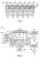
- FIG. 7is a cross-sectional view of the multi-layered structure, shown in FIG. 6 , after being subjected to a blanket etch process, in accordance with the present invention
- FIG. 8is a simplified plan view of an etch chamber that may be employed to practice the present invention.
- FIG. 9cross-sectional view of the multi-layered structure, shown in FIG. 7 , after being subjected to an anisotropic etch process, in accordance with the prior art.
- FIG. 10is a cross-sectional view of the multi-layered structure, shown in FIG. 9 , after subjecting the same to etch processes to expose areas of the underlying substrate.
- Multi-layered structure 10comprises a substrate 12 , having one or more existing layers thereon, shown as a layer 14 , and a patterned layer 16 .
- Layer 14is disposed between substrate 12 and patterned layer 16 .
- Substrate 12may be formed from materials including, but not limited to, silicon, gallium arsenide, quartz, fused-silica, sapphire, organic polymers, siloxane polymers, borosilicate glass, fluorocarbon polymers or a combination thereof.
- Primer layer 14may be formed from any known material, such as aluminum, silicon nitride, a native oxide and the like.
- layer 14functions to provide a standard interface between substrate 12 and patterned layer 16 , thereby reducing the need to customize each process to the material upon which patterned layer 16 is to be deposited upon.
- layer 14may be formed from a material with the same etch characteristics as patterned layer 16 .
- Layer 14is fabricated in such a manner so as to possess a continuous, smooth, if not planar, relatively defect-free surface that may exhibit excellent adhesion to patterned layer 16 . Additionally, layer 14 has a substantially uniform thickness.
- An exemplary composition for layer 14is available from Brewer Science, Inc. of Rolla, Mo.
- Layer 14may be deposited upon substrate 12 using any suitable method including, but not limited to, chemical vapor deposition (CVD), physical vapor deposition (PVD), sputter deposition, spin-coating, and dispensing of a liquid.
- CVDchemical vapor deposition
- PVDphysical vapor deposition
- sputter depositionspin-coating
- dispensing of a liquidany suitable method including, but not limited to, chemical vapor deposition (CVD), physical vapor deposition (PVD), sputter deposition, spin-coating, and dispensing of a liquid.
- IMPRIO 250TMAn exemplary lithographic system utilized in imprint lithography is available under the trade name IMPRIO 250TM from Molecular Imprints, Inc., having a place of business at 1807-C Braker Lane, Suite 100, Austin, Tex. 78758.
- the system description for the IMPRIO 250TMis available at www.molecularimprints.com and is incorporated herein by reference.
- planarization layer 24is formed upon patterned layer 16 , forming multi-layered structure 110 .
- Planarization layer 24may be formed upon patterned layer 16 in any of the methods mentioned above with respect to primer layer 14 .
- planarization layer 26may comprise an organic polymerizable resist.
- planarization layer 24may be formed from a silicon-containing polymerizable material. Exemplary materials from which patterned layer 16 and planarization layer 24 may be formed are disclosed in U.S. patent application Ser. No. 10/789,319, entitled “Composition for an Etching Mask Comprising a Silicon-Containing Material,” having Frank Xu, Michael N. Miller and Michael P. C. Watts listed as inventors and which is incorporated by reference herein.
- patterned layer 16may be formed from a silicon-free materials and consists of the following:
- isobornyl acrylatecomprises approximately 55% of the composition
- n-hexyl acrylatecomprises approximately 27%
- ethylene glycol diacrylatecomprises approximately 15%
- the initiator 2-hydroxy-2-methyl-1-phenyl-propan-1-onecomprises approximately 3%.
- the initiatoris sold under the trade name DAROCUR® 1173 by CIBA® of Tarrytown, N.Y.
- the above-identified compositionalso includes stabilizers that are well known in the chemical art to increase the operational life of the composition.
- a surfactantis defined as any molecule, one tail of which is hydrophobic.
- Surfactantsmay be either fluorine containing, e.g., include a fluorine chain, or may not include any fluorine in the surfactant molecule structure.
- the ZONYL® FSO-100 additivecomprises less than 1% of the composition, with the relative amounts of the remaining components being as discussed above with respect to COMPOSITION 1. However, the percentage of ZONYL® FSO-100 may be greater than 1%.
- Planarization layer 24may be formed from a silicon-containing material that is suitable for deposition upon patterned layer 16 employing spin-coating technique.
- Exemplary compositions from which to form planarization layer 24are as follows:
- hydroxyl-functional polysiloxanecomprises approximately 4% of the composition, hexamethoxymethylmelamine comprises approximately 0.95%, toluenesulfonic acid comprises approximately 0.05% and methyl amyl ketone comprises approximately 95%.
- hydroxyl-functional polysiloxanecomprises approximately 4% of the composition, hexamethoxymethylmelamine comprisies approximately 0.7%, gamma-glycidoxypropyltrimethoxysilane comprisies approximately 0.25%, toluenesulfonic acid comprises approximately 0.05%, and methyl amyl ketone comprises approximately 95%.
- Both COMPOSITIONS 3 and 4are made up of at least 4% of the silicone resin. Upon curing, however, the quantity of silicon present in conformal layer 58 is at least 5% by weight and typically in a range of 20% or greater. Specifically, the quantity and composition of the solvent present in COMPOSITIONS 3 and 4 is selected so that a substantial portion of the solvent evaporates during spin-coating application of the COMPOSITION 3 or 4 on solidified imprinting layer 134 . In the present exemplary silicon-containing material, approximately 90% of the solvent evaporates during spin-coating. Upon exposing the silicon-containing material to thermal energy, the remaining 10% of the solvent evaporates, leaving conformal layer 58 with approximately 20% silicon by weight.
- planarization layer 24includes first and second opposed sides.
- First side 26faces patterned layer 16 and has a profile complementary to the profile of patterned layer 16 .
- Second side 28faces away from patterned layer 16 .
- second side 28has a substantially normalized profile.
- distances k 1 , k 3 , k 5 , k 7 , kg, and k 11 between protrusions 18 and second side 28are substantially the same and the distances k 2 , k 4 , k 6 , k 8 , and k 10 between recessions 20 and second side 28 are substantially the same.
- planarization layer 24is exposed to actinic energy to polymerize and, therefore, to solidify the same.
- actinic energyincludes ultraviolet, thermal, electromagnetic, visible light, heat, and the like. The selection of actinic energy depends on the materials from which planarization layer 24 is formed. After solidification of planarization layer, planarizing mold (not shown) is separated therefrom.
- planarization layer 24does not adhere to the planarizing mold (not shown)
- a low surface energy coatingsuch as a diamond-like layer
- the planarization mold (not shown)may be formed from a material having a low surface energy, e.g., diamond.
- release properties of planarization layer 24may be improved by including in the material from which the same is fabricated the aforementioned surfactant.
- the surfactantprovides the desired release properties to reduce adherence of planarization layer 24 to the planarizing mold (not shown). It should be understood that the surfactant may be used in conjunction with, or in lieu of, the low surface energy coating that may be applied to the planarizing mold (not shown).
- multi-layered structure 110is subjected to an isotropic or anisotropic etch to remove portions of planarization layer 24 to provide multi-layered structure 110 with a crown surface 30 of etched structure 111 .
- Crown surface 30is defined by an exposed surface 32 of each of protrusions 18 and surface 34 of areas 35 of planarization layer 24 that remain after certain etch processes.
- Surfaces 34have a width ‘w 1 ’.
- etched structure 111is subjected to an anisotropic etch.
- the etch chemistry of the anisotropic etchis selected to maximize etching of protrusions 18 and the segments of patterned layer 16 in superimposition therewith, while minimizing etching of the areas 35 .
- regions 36 of substrate 12 in superimposition with protrusions 18are exposed forming a multi-layered structure 210 .
- Multi-layered structure 210comprises protrusions 38 , each of which has an upper region 31 and a nadir region 33 .
- Upper region 31is fabricated from portions of areas 35 that remain.
- Nadir regions 33comprise patterned layer 16 and primer layer 14 in superimposition with areas 35 .
- Protrusions 138have a width ‘w 2 ’. Ideally, width ‘w 2 ’ is substantially the same as width ‘w 1 ’ of portions 34 .
- width ‘w 3 ’is greater than width ‘w 4 ,’ however; width ‘w 3 ’ may be smaller than width ‘w 4 .’
- the variation of width ‘w 3 ’ as compared to width ‘w 4 ’may be as a result of subjecting crown surface 30 , shown in FIG. 3 , to the aforementioned anisotropic etch.
- the difference in widthmay be due to any one or more of several factors, including swelling of upper region 131 in response to the etch chemistry employed to form protrusions 138 .
- Alternatively, or in addition to the aforementioned swelling, undercutting, and/or sputtering of nadir region 133may occur during formation of protrusions 138 .
- a liner layeris employed to substantially surround exposed sides of the segments of upper region 131 .
- a liner layer for purposes of the present inventionis to be defined as a layer that substantially conforms to the shape of the surface upon which it is disposed and substantially insulates the material from desired processes. Typically, liner layer is thinner than the layer upon which it is disposed.
- a liner layer 40is formed so that same may be present between patterned layer 16 and planarization layer 24 , forming multi-layered structure 310 .
- liner layer 40is deposited on patterned layer 16 .
- An exemplary liner layer 40would have a relative thickness and etch rate differential, compared to patterned layer 16 and/or planarization layer 24 , which enables formation of a desired pattern in primer layer 14 and/or substrate 12 .
- the pattern formed thereincorresponds to the pattern in patterned layer 16 .
- liner layer 40has a thickness in a range of 5 nm to 100 nm, inclusive and provides an etch rate differential of no less than 10:1.
- the etch rate of the liner layer 40may be ten times faster than the etch rate of patterned layer 16 and/or planarization layer 24 .
- the etch rate of liner layer 40may be ten times slower than the etch rate of patterned layer 16 and/or planarization layer 24 . In this manner, liner layer 40 functions as a hard mask.
- exemplary material from which to form liner layer 40includes silicon dioxide (SiO 2 ), silicon nitride (SiN) and silicon oxynitride (SiON) It is desired that liner layer 40 be formed from processes that would not compromise the structural integrity of patterned layer 16 and/or planarization layer 24 . For example, were patterned layer 16 formed from COMPOSITION 1 or COMPOSITION 2, it would be desired that the process employed to deposit liner layer 40 employs temperatures no greater than 150 degrees Celsius. An exemplary process by which to deposit liner layer 40 formed from SiO 2 is discussed by J. W. Klaus and S. M.
- multi-layered structure 310is subjected to an etch process to remove portions of planarization layer 24 to provide a multi-layered structure 410 with a crown surface 230 , wherein the isotropic etch may be an O 2 etch.
- multi-layered structure 310may be deposited in an inductively coupled plasma etch reactor 330 , shown in FIG. 8 .
- reactor 330includes upper 332 and lower 333 bodies and a cover 334 , which defines a chamber 336 .
- Cover 334includes a dielectric window 338 and a coil 340 disposed proximate to dielectric window 338 .
- Multi-layered structure 310is supported within chamber 336 by a pedestal 342 or chuck, with dielectric window 338 disposed between structure 310 and coil 340 .
- Coil 334typically includes multiple windings and is connected to a radio frequency (RF) power generator 344 through an impedance matching network 346 to provide RF power into chamber 336 .
- RFradio frequency
- a bias RF power generator 348 and associated impedance matching circuit 350is connected to pedestal 342 and used to impose a bias on multi-layer structure 310 .
- Upper body 332is composed of dielectric material, typically quartz or ceramic, so as to minimize attenuation of the RF power coupled into chamber 336 .
- Lower body 333surrounds pedestal 342 and is formed from electrically conductive material. Lower body 333 coupled to ground functions as the ground for the RF power supplied to pedestal 342 .
- cooling channels 352formed within the lower body 333 and pedestal 342 . A supply of coolant fluid 353 may be pumped through channels 352 to transfer heat away from the interior of chamber 336 and/or pedestal 342 to control the temperature thereof.
- the temperature of upper body 332may be controlled by forced air convection/conduction methods.
- a source 354 of etchant gasesis in fluid communication with chamber 336 through gas injection ports 356 .
- a vacuum pump 358is in fluid communication with chamber 336 to control the pressure of the atmosphere therein.
- An exemplary reactor that may be employedis available from Oxford Instruments America, Inc. 130 Baker Avenue, Concord, Mass. 01742 under the product name PLASMALAB 80 PLUS.
- crown surface 230is formed by exposing multi-layered structure 310 to an etch chemistry that includes oxygen flowed into chamber 336 at a rate of approximately 30 standard cubic centimeters per minute (sccm), CHF 3 flowed into chamber 336 at a rate of approximately 12 sccm.
- RF power 344is established to be at 45 Watts at 13.56 MHz, and DC bias 350 is set at ⁇ 185 volts.
- Pump 358establishes a chamber pressure of approximately 20 Torr, and pedestal 342 is maintained at a temperature of approximately ⁇ 8° C. With these parameters, crown surface 230 is formed in approximately 4 minutes and 40 seconds.
- Were planarization layer formed from one of COMPOSITIONS 1 and 2, i.e., without any silicon being present, the same etch parameters mentioned abovemay be employed excepting that CHF 3 is not introduced into chamber 336 .
- crown surface 230is defined by exposed regions of liner layer 40 and regions 233 that remain of planarization layer 64 after being exposed to the isotropic O 2 etch.
- Exposed regions of liner layer 40include surfaces of first portions 232 , which are in superimposition with protrusions 18 and surfaces of second portions 235 .
- Second portions 235are disposed on opposed ends of first portion 232 and in superimposition with recession 20 . Extending between subsets of adjacent second portions 235 are nadir portions 237 .
- an anisotropic etchis employed to substantially remove first portion 232 and surfaces of second portions 235 .
- multi-layered structure 410is subjected to an etching environment in chamber 336 by establishing RF power 344 to be approximately 50 Watts at 13.56 MHz, DC bias 350 to be approximately ⁇ 196 volts, chamber pressure at approximately 30 Torr, with the oxygen flow being terminated.
- Pedestal 342is maintained at a temperature of approximately ⁇ 8° C.
- the battlement surfaceis defined by exposed surfaces 342 in regions of patterned layer 16 that were in superimposition with protrusions 18 , as well as surfaces 334 of remaining portions of regions 133 and surfaces 336 the remaining areas of second portions 235 .
- An extent of second portions 235 , extending between surface 336 and surface 342define sidewalls 344 .
- Pedestal 342is maintained at a temperature of approximately ⁇ 8° C. With these parameters a multi-layered structure 610 is formed by exposure of multi-layered structure 510 to this etching environment for approximately 6 minutes. More specifically, portions of primer layer 14 and patterned layer 16 in superimposition with exposed surfaces 342 are removed. As a result, areas 548 of substrate 12 in superimposition with exposed surfaces 342 are exposed, leaving spaced-apart protrusions 650 . Each protrusion 650 includes a sub-portion 614 of planarization layer 14 , a sub-portion 616 of patterned layer 16 and an upper portion 610 .
- Upper portion 610includes a sub-portion 612 of sidewall 344 , nadir portion 237 and the remaining portions of region 133 in superimposition with nadir portion 237 .
- a width ‘w 5 ’ of upper portion 610is substantially equal to a width ‘w 6 ’ of lower portion.
- sub-portions 612ensures that width ‘w 5 ’ is substantially the same as width ‘w 6 ,’ as desired. In this manner, width ‘w 5 ’ and, therefore, width ‘w 6 ’ may be substantially the same as width ‘w 1 ,’ shown in FIG. 3 .
- planarization layer 24may be formed from a silicon-containing polymerizable material. More specifically, planarization layer 24 may be formed from a silicon-containing spin-on material. Therefore, the aforementioned isotropic etch to remove portions of planarization layer 24 to provide multi-layered structure 410 may be a halogen etch. Also, multi-layered structure 610 may be utilized in a lift-off process.
Landscapes
- Engineering & Computer Science (AREA)
- Physics & Mathematics (AREA)
- Condensed Matter Physics & Semiconductors (AREA)
- General Physics & Mathematics (AREA)
- Manufacturing & Machinery (AREA)
- Computer Hardware Design (AREA)
- Microelectronics & Electronic Packaging (AREA)
- Power Engineering (AREA)
- Drying Of Semiconductors (AREA)
- Micromachines (AREA)
Abstract
Description
- The field of the invention relates generally to semiconductor processing. More particularly, the present invention is directed to a method of controlling the critical dimension of structures formed on a substrate.
- Micro-fabrication involves the fabrication of very small structures, e.g., having features on the order of micro-meters or smaller. One area in which micro-fabrication has had a sizeable impact is in the processing of integrated circuits. As the semiconductor processing industry continues to strive for larger production yields while increasing the circuits per unit area formed on a substrate, micro-fabrication becomes increasingly important. Micro-fabrication provides greater process control while allowing increased reduction of the critical dimension of the structures formed. Other areas of development in which micro-fabrication has been employed include biotechnology, optical technology, mechanical systems, and the like.
- As the critical dimension of structures formed on substrates is reduced, there is an increasing desire to control the same. A method of controlling the critical dimension of semiconductor devices is described in U.S. Pat. No. 6,245,581 to Bonser et al. Bonser et al. describes a method and an apparatus for controlling critical dimensions. More specifically, a run of semiconductor devices is processed, a critical dimension measurement is performed upon at least one of the processed semiconductor devices, an analysis of the critical dimension is performed, and a second process upon the semiconductor devices in response to the critical dimension analysis is performed.
- Another method of controlling the critical dimension of semiconductor devices is described in U.S. Pat. No. 5,926,690 to Toprac et al. Toprac et al. describes a control method employing a control system using photoresist etch time as a manipulated variable in either a feed-forward or a feedback control configuration to control critical dimension variation during semiconductor fabrication.
- It is desired, therefore, to provide an improved method of controlling the critical dimension of structures formed on a substrate.
- The present invention provides a method of patterning a substrate, the method including, inter alia, forming a multi-layered structure on the substrate formed from first, second and third materials. The first, second and third materials are exposed to an etch chemistry, with the first and second materials having a common etch rate along a first direction, defining a first etch rate, and the first and third materials having a similar etch rate along a second direction, transversely extending to the first direction, defining a second etch rate. Typically, the etch rate is selected to be different in furtherance of facilitating control of the dimensions of features formed during the etching process. These embodiments and others are described more fully below.
FIG. 1 is a cross-sectional view of a prior art bi-layer structure;FIG. 2 is a cross-sectional view of the bi-layer structure, shown inFIG. 1 , having a planarization layer disposed thereon to form a multi-layered structure;FIG. 3 is a cross-sectional view of the multi-layered structure, shown inFIG. 2 , after being subjected to a blanket etch, forming etched structure, in accordance with the prior art;FIG. 4 is a cross-sectional view of the etched structure, shown inFIG. 3 , after being subjected to an anisotropic etch process, in accordance with the prior art;FIG. 5 is a cross-sectional view of the etched structure, shown inFIG. 3 , demonstrating critical-dimension control characteristics that were recognized and attenuated, in accordance with the present invention;FIG. 6 is a cross-sectional view of a multi-layered structure formed in accordance with the present invention;FIG. 7 is a cross-sectional view of the multi-layered structure, shown inFIG. 6 , after being subjected to a blanket etch process, in accordance with the present invention;FIG. 8 is a simplified plan view of an etch chamber that may be employed to practice the present invention;FIG. 9 cross-sectional view of the multi-layered structure, shown inFIG. 7 , after being subjected to an anisotropic etch process, in accordance with the prior art; andFIG. 10 is a cross-sectional view of the multi-layered structure, shown inFIG. 9 , after subjecting the same to etch processes to expose areas of the underlying substrate.- Referring to
FIG. 1 , amulti-layered structure 10 is shown.Multi-layered structure 10 comprises asubstrate 12, having one or more existing layers thereon, shown as alayer 14, and a patternedlayer 16.Layer 14 is disposed betweensubstrate 12 and patternedlayer 16.Substrate 12 may be formed from materials including, but not limited to, silicon, gallium arsenide, quartz, fused-silica, sapphire, organic polymers, siloxane polymers, borosilicate glass, fluorocarbon polymers or a combination thereof. Primer layer 14 may be formed from any known material, such as aluminum, silicon nitride, a native oxide and the like. In the present example,layer 14 functions to provide a standard interface betweensubstrate 12 and patternedlayer 16, thereby reducing the need to customize each process to the material upon which patternedlayer 16 is to be deposited upon. In addition,layer 14 may be formed from a material with the same etch characteristics as patternedlayer 16.Layer 14 is fabricated in such a manner so as to possess a continuous, smooth, if not planar, relatively defect-free surface that may exhibit excellent adhesion to patternedlayer 16. Additionally,layer 14 has a substantially uniform thickness. An exemplary composition forlayer 14 is available from Brewer Science, Inc. of Rolla, Mo. under the trade name DUV30J-6.Layer 14 may be deposited uponsubstrate 12 using any suitable method including, but not limited to, chemical vapor deposition (CVD), physical vapor deposition (PVD), sputter deposition, spin-coating, and dispensing of a liquid.Patterned layer 16 may compriseprotrusions 18 andrecessions 20 forming a pattern on asurface 22 of patternedlayer 16, withrecessions 20 extending along a direction parallel toprotrusions 18 providing a cross-section of patternedlayer 16 with a shape of a battlement. However,protrusions 18 andrecessions 20 may correspond to virtually any feature required to create an integrated circuit and may be as small as a few nanometers. The pattern onsurface 22 of patternedlayer 16 may be formed by such techniques including, but not limited to, photolithography, e-beam lithography, x-ray lithography, ion beam lithography, and imprint lithography. Imprint lithography is described in detail in numerous publications, such as United States published patent application 2004/0065976, entitled, “Method and a Mold to Arrange Features on a Substrate to Replicate Features having Minimal Dimensional Variability”; 2004/0065252, entitled “Method of Forming a Layer on a Substrate to Facilitate Fabrication of Metrology Standards”; and 2004/0046271, entitled “Method and a Mold to Arrange Features on a Substrate to Replicate Features having Minimal Dimensional Variability”, all of which are assigned to the assignee of the present invention. An exemplary lithographic system utilized in imprint lithography is available under the trade name IMPRIO 250™ from Molecular Imprints, Inc., having a place of business at 1807-C Braker Lane, Suite 100, Austin, Tex. 78758. The system description for the IMPRIO 250™ is available at www.molecularimprints.com and is incorporated herein by reference.- Referring to
FIG. 2 , aplanarization layer 24 is formed upon patternedlayer 16, formingmulti-layered structure 110.Planarization layer 24 may be formed upon patternedlayer 16 in any of the methods mentioned above with respect toprimer layer 14. In a first embodiment,planarization layer 26 may comprise an organic polymerizable resist. However, in a further embodiment,planarization layer 24 may be formed from a silicon-containing polymerizable material. Exemplary materials from which patternedlayer 16 andplanarization layer 24 may be formed are disclosed in U.S. patent application Ser. No. 10/789,319, entitled “Composition for an Etching Mask Comprising a Silicon-Containing Material,” having Frank Xu, Michael N. Miller and Michael P. C. Watts listed as inventors and which is incorporated by reference herein. For example, patternedlayer 16 may be formed from a silicon-free materials and consists of the following: - In COMPOSITION 1, isobornyl acrylate comprises approximately 55% of the composition, n-hexyl acrylate comprises approximately 27%, ethylene glycol diacrylate comprises approximately 15% and the initiator 2-hydroxy-2-methyl-1-phenyl-propan-1-one comprises approximately 3%. The initiator is sold under the trade name DAROCUR® 1173 by CIBA® of Tarrytown, N.Y. The above-identified composition also includes stabilizers that are well known in the chemical art to increase the operational life of the composition.
- Release properties of COMPOSITION 1 may be improved by including a surfactant. For purposes of this invention a surfactant is defined as any molecule, one tail of which is hydrophobic. Surfactants may be either fluorine containing, e.g., include a fluorine chain, or may not include any fluorine in the surfactant molecule structure. An exemplary surfactant is available under the trade name ZONYL® FSO-100 from DUPONT that has a general structure of R1R2where R1=F(CF2CF2)Y, with y being in a range of 1 to 7, inclusive and R2=CH2CH2O(CH2CH2O)XH, where X is in a range of 0 to 15, inclusive. This provides
material 40 with the following composition: - The ZONYL® FSO-100 additive comprises less than 1% of the composition, with the relative amounts of the remaining components being as discussed above with respect to COMPOSITION 1. However, the percentage of ZONYL® FSO-100 may be greater than 1%.
Planarization layer 24 may be formed from a silicon-containing material that is suitable for deposition upon patternedlayer 16 employing spin-coating technique. Exemplary compositions from which to formplanarization layer 24 are as follows:- In COMPOSITION 3, hydroxyl-functional polysiloxane comprises approximately 4% of the composition, hexamethoxymethylmelamine comprises approximately 0.95%, toluenesulfonic acid comprises approximately 0.05% and methyl amyl ketone comprises approximately 95%. In
COMPOSITION 4, hydroxyl-functional polysiloxane comprises approximately 4% of the composition, hexamethoxymethylmelamine comprisies approximately 0.7%, gamma-glycidoxypropyltrimethoxysilane comprisies approximately 0.25%, toluenesulfonic acid comprises approximately 0.05%, and methyl amyl ketone comprises approximately 95%. - Both
COMPOSITIONS 3 and 4 are made up of at least 4% of the silicone resin. Upon curing, however, the quantity of silicon present in conformal layer58 is at least 5% by weight and typically in a range of 20% or greater. Specifically, the quantity and composition of the solvent present inCOMPOSITIONS 3 and 4 is selected so that a substantial portion of the solvent evaporates during spin-coating application of theCOMPOSITION 3 or 4 on solidified imprinting layer134. In the present exemplary silicon-containing material, approximately 90% of the solvent evaporates during spin-coating. Upon exposing the silicon-containing material to thermal energy, the remaining 10% of the solvent evaporates, leaving conformal layer58 with approximately 20% silicon by weight. - Referring to
FIGS. 1 and 2 ,planarization layer 24 includes first and second opposed sides.First side 26 faces patternedlayer 16 and has a profile complementary to the profile of patternedlayer 16.Second side 28 faces away from patternedlayer 16. As shown inFIG. 2 ,second side 28 has a substantially normalized profile. To providesecond side 28 with a substantially normalized profile, distances k1, k3, k5, k7, kg, and k11betweenprotrusions 18 andsecond side 28 are substantially the same and the distances k2, k4, k6, k8, and k10betweenrecessions 20 andsecond side 28 are substantially the same. One manner in which to providesecond side 28 with a normalized profile is to contactplanarization layer 24 with a planarizing mold (not shown) having a smooth, if not planar, surface.Planarization layer 24 is exposed to actinic energy to polymerize and, therefore, to solidify the same. Exemplary actinic energy includes ultraviolet, thermal, electromagnetic, visible light, heat, and the like. The selection of actinic energy depends on the materials from whichplanarization layer 24 is formed. After solidification of planarization layer, planarizing mold (not shown) is separated therefrom. To ensure thatplanarization layer 24 does not adhere to the planarizing mold (not shown), a low surface energy coating, such as a diamond-like layer, may be deposited upon the planarizing mold (not shown) or the planarization mold (not shown) may be formed from a material having a low surface energy, e.g., diamond. Alternatively, release properties ofplanarization layer 24 may be improved by including in the material from which the same is fabricated the aforementioned surfactant. The surfactant provides the desired release properties to reduce adherence ofplanarization layer 24 to the planarizing mold (not shown). It should be understood that the surfactant may be used in conjunction with, or in lieu of, the low surface energy coating that may be applied to the planarizing mold (not shown). - Referring to
FIGS. 2 and 3 ,multi-layered structure 110 is subjected to an isotropic or anisotropic etch to remove portions ofplanarization layer 24 to providemulti-layered structure 110 with acrown surface 30 ofetched structure 111.Crown surface 30 is defined by an exposedsurface 32 of each ofprotrusions 18 andsurface 34 ofareas 35 ofplanarization layer 24 that remain after certain etch processes.Surfaces 34 have a width ‘w1’. - Referring to
FIGS. 3 and 4 , etchedstructure 111 is subjected to an anisotropic etch. The etch chemistry of the anisotropic etch is selected to maximize etching ofprotrusions 18 and the segments of patternedlayer 16 in superimposition therewith, while minimizing etching of theareas 35. As a result,regions 36 ofsubstrate 12 in superimposition withprotrusions 18 are exposed forming amulti-layered structure 210.Multi-layered structure 210 comprisesprotrusions 38, each of which has anupper region 31 and anadir region 33.Upper region 31 is fabricated from portions ofareas 35 that remain.Nadir regions 33 comprise patternedlayer 16 andprimer layer 14 in superimposition withareas 35.Protrusions 138 have a width ‘w2’. Ideally, width ‘w2’ is substantially the same as width ‘w1’ ofportions 34. - Referring to
FIGS. 4 and 5 , obtaining ideal dimensions of widths w1and w2is often problematic. For example, it has often been found thatupper region 131 has a width ‘w3’ that differs from the width ‘w4’ ofnadir region 133. As shown inFIG. 5 , width ‘w3’ is greater than width ‘w4,’ however; width ‘w3’ may be smaller than width ‘w4.’ The variation of width ‘w3’ as compared to width ‘w4’ may be as a result of subjectingcrown surface 30, shown inFIG. 3 , to the aforementioned anisotropic etch. The difference in width may be due to any one or more of several factors, including swelling ofupper region 131 in response to the etch chemistry employed to formprotrusions 138. Alternatively, or in addition to the aforementioned swelling, undercutting, and/or sputtering ofnadir region 133 may occur during formation ofprotrusions 138. Nonetheless, it is desired to have width ‘w3’ be substantially the same as width ‘w4,’ and thus, width ‘w3’ substantially the same as width ‘w1,’ shown inFIG. 3 . To that end, a liner layer is employed to substantially surround exposed sides of the segments ofupper region 131. A liner layer for purposes of the present invention is to be defined as a layer that substantially conforms to the shape of the surface upon which it is disposed and substantially insulates the material from desired processes. Typically, liner layer is thinner than the layer upon which it is disposed. - Referring to
FIG. 6 , aliner layer 40 is formed so that same may be present between patternedlayer 16 andplanarization layer 24, formingmulti-layered structure 310. To that end,liner layer 40 is deposited on patternedlayer 16. Anexemplary liner layer 40 would have a relative thickness and etch rate differential, compared to patternedlayer 16 and/orplanarization layer 24, which enables formation of a desired pattern inprimer layer 14 and/orsubstrate 12. Typically, the pattern formed therein corresponds to the pattern in patternedlayer 16. In the present example,liner layer 40 has a thickness in a range of 5 nm to 100 nm, inclusive and provides an etch rate differential of no less than 10:1. For example, the etch rate of theliner layer 40, for a given etch chemistry, may be ten times faster than the etch rate of patternedlayer 16 and/orplanarization layer 24. Alternatively, the etch rate ofliner layer 40, for a given etch chemistry, may be ten times slower than the etch rate of patternedlayer 16 and/orplanarization layer 24. In this manner,liner layer 40 functions as a hard mask. To that end, exemplary material from which to formliner layer 40 includes silicon dioxide (SiO2), silicon nitride (SiN) and silicon oxynitride (SiON) It is desired thatliner layer 40 be formed from processes that would not compromise the structural integrity of patternedlayer 16 and/orplanarization layer 24. For example, were patternedlayer 16 formed from COMPOSITION 1 or COMPOSITION 2, it would be desired that the process employed to depositliner layer 40 employs temperatures no greater than 150 degrees Celsius. An exemplary process by which to depositliner layer 40 formed from SiO2is discussed by J. W. Klaus and S. M. George in the article entitled “SiO2Chemical Vapor Deposition at Room Temperatures Using SiCl4and H2O with an NH3Catalyst,” Journal of the Electrochemical Society, 147(7) 2658-2664 (2000). An exemplary process by which to depositliner layer 40 formed from SiN is discussed by G. P. Li and Huinan Guan in an article entitled “Exploring Low Temperature High Density Inductive Coupled Plasma Chemical Vapor Deposition (HDICPCVD) Dielectric Films for MMICs,” project Report 2002-03 for MICRO Project 02-241, Department of Electrical & Computer Engineering, University of California, Irvine, Calif. After formation ofliner layer 40,planarization 24 is disposed atop thereof, as discussed above. - Referring to
FIGS. 6 and 7 ,multi-layered structure 310 is subjected to an etch process to remove portions ofplanarization layer 24 to provide amulti-layered structure 410 with acrown surface 230, wherein the isotropic etch may be an O2etch. To that end,multi-layered structure 310 may be deposited in an inductively coupledplasma etch reactor 330, shown inFIG. 8 . - Referring to
FIG. 8 ,reactor 330 includes upper332 and lower333 bodies and acover 334, which defines achamber 336. Cover334 includes adielectric window 338 and acoil 340 disposed proximate todielectric window 338.Multi-layered structure 310 is supported withinchamber 336 by apedestal 342 or chuck, withdielectric window 338 disposed betweenstructure 310 andcoil 340.Coil 334 typically includes multiple windings and is connected to a radio frequency (RF)power generator 344 through animpedance matching network 346 to provide RF power intochamber 336. In addition, a biasRF power generator 348 and associatedimpedance matching circuit 350 is connected topedestal 342 and used to impose a bias onmulti-layer structure 310.Upper body 332 is composed of dielectric material, typically quartz or ceramic, so as to minimize attenuation of the RF power coupled intochamber 336.Lower body 333 surroundspedestal 342 and is formed from electrically conductive material.Lower body 333 coupled to ground functions as the ground for the RF power supplied topedestal 342. Also included are coolingchannels 352 formed within thelower body 333 andpedestal 342. A supply ofcoolant fluid 353 may be pumped throughchannels 352 to transfer heat away from the interior ofchamber 336 and/orpedestal 342 to control the temperature thereof. The temperature ofupper body 332 may be controlled by forced air convection/conduction methods. Asource 354 of etchant gases is in fluid communication withchamber 336 throughgas injection ports 356. Avacuum pump 358 is in fluid communication withchamber 336 to control the pressure of the atmosphere therein. An exemplary reactor that may be employed is available from Oxford Instruments America, Inc. 130 Baker Avenue, Concord, Mass. 01742 under the product name PLASMALAB 80 PLUS. - Referring to
FIGS. 6, 7 and8, assumingplanarization layer 24 is formed from one ofCOMPOSITIONS 3 and 4,crown surface 230 is formed by exposingmulti-layered structure 310 to an etch chemistry that includes oxygen flowed intochamber 336 at a rate of approximately 30 standard cubic centimeters per minute (sccm), CHF3flowed intochamber 336 at a rate of approximately 12 sccm.RF power 344 is established to be at 45 Watts at 13.56 MHz, and DC bias350 is set at −185 volts.Pump 358 establishes a chamber pressure of approximately 20 Torr, andpedestal 342 is maintained at a temperature of approximately −8° C. With these parameters,crown surface 230 is formed in approximately 4 minutes and 40 seconds. Were planarization layer formed from one of COMPOSITIONS 1 and 2, i.e., without any silicon being present, the same etch parameters mentioned above may be employed excepting that CHF3is not introduced intochamber 336. - As a result of
etching planarization layer 24,crown surface 230 is defined by exposed regions ofliner layer 40 andregions 233 that remain of planarization layer64 after being exposed to the isotropic O2etch. Exposed regions ofliner layer 40 include surfaces offirst portions 232, which are in superimposition withprotrusions 18 and surfaces ofsecond portions 235.Second portions 235 are disposed on opposed ends offirst portion 232 and in superimposition withrecession 20. Extending between subsets of adjacentsecond portions 235 arenadir portions 237. - Referring to
FIGS. 7-9 , an anisotropic etch is employed to substantially removefirst portion 232 and surfaces ofsecond portions 235. To that end,multi-layered structure 410 is subjected to an etching environment inchamber 336 by establishingRF power 344 to be approximately 50 Watts at 13.56 MHz, DC bias350 to be approximately −196 volts, chamber pressure at approximately 30 Torr, with the oxygen flow being terminated.Pedestal 342 is maintained at a temperature of approximately −8° C. With these parameters amulti-layered structure 510 having a surface with a shape of a battlement is formed by exposure ofmulti-layered structure 410 to this etching environment for approximately 1 minute and ten seconds. The battlement surface is defined by exposedsurfaces 342 in regions of patternedlayer 16 that were in superimposition withprotrusions 18, as well assurfaces 334 of remaining portions ofregions 133 andsurfaces 336 the remaining areas ofsecond portions 235. An extent ofsecond portions 235, extending betweensurface 336 andsurface 342 definesidewalls 344. - Referring to
FIGS. 9 and 10 , an anisotropic etch is employed to remove portions ofmulti-layered structure 510 in superimposition with exposedsurfaces 342, formingmulti-layered structure 610. To that end,multi-layered structure 510 is subjected to an etching environment inchamber 336 by establishingRF power 344 to be approximately 130 Watts at 13.56 MHz, DC bias350 to be approximately −380 volts, chamber pressure at approximately 6 Torr, with the CHF3being replaced by a flow of argon and oxygen. The argon is flowed intochamber 336 at a rate of approximately 30 sccm and the oxygen at a rate of approximately 3 sccm.Pedestal 342 is maintained at a temperature of approximately −8° C. With these parameters amulti-layered structure 610 is formed by exposure ofmulti-layered structure 510 to this etching environment for approximately 6 minutes. More specifically, portions ofprimer layer 14 and patternedlayer 16 in superimposition with exposedsurfaces 342 are removed. As a result,areas 548 ofsubstrate 12 in superimposition with exposedsurfaces 342 are exposed, leaving spaced-apartprotrusions 650. Eachprotrusion 650 includes asub-portion 614 ofplanarization layer 14, asub-portion 616 of patternedlayer 16 and anupper portion 610.Upper portion 610 includes asub-portion 612 ofsidewall 344,nadir portion 237 and the remaining portions ofregion 133 in superimposition withnadir portion 237. A width ‘w5’ ofupper portion 610 is substantially equal to a width ‘w6’ of lower portion. Specifically, sub-portions612 ensures that width ‘w5’ is substantially the same as width ‘w6,’ as desired. In this manner, width ‘w5’ and, therefore, width ‘w6’ may be substantially the same as width ‘w1,’ shown inFIG. 3 . - In a further embodiment,
planarization layer 24 may be formed from a silicon-containing polymerizable material. More specifically,planarization layer 24 may be formed from a silicon-containing spin-on material. Therefore, the aforementioned isotropic etch to remove portions ofplanarization layer 24 to providemulti-layered structure 410 may be a halogen etch. Also,multi-layered structure 610 may be utilized in a lift-off process. - The embodiments of the present invention described above are exemplary. Many changes and modification may be made to the disclosure recited above, while remaining within the scope of the invention. The scope of the invention should, therefore, be determined not with reference to the above description, but instead should be determined with reference to the appended claims along with their full scope of equivalents.
Claims (23)
Priority Applications (3)
| Application Number | Priority Date | Filing Date | Title |
|---|---|---|---|
| US11/184,664US7256131B2 (en) | 2005-07-19 | 2005-07-19 | Method of controlling the critical dimension of structures formed on a substrate |
| PCT/US2006/021949WO2007011468A1 (en) | 2005-07-19 | 2006-06-05 | Method of controlling the critical dimension of structures formed on a substrate |
| TW095121222ATW200707540A (en) | 2005-07-19 | 2006-06-14 | Method of controlling the critical dimension of structures formed on a substrate |
Applications Claiming Priority (1)
| Application Number | Priority Date | Filing Date | Title |
|---|---|---|---|
| US11/184,664US7256131B2 (en) | 2005-07-19 | 2005-07-19 | Method of controlling the critical dimension of structures formed on a substrate |
Publications (2)
| Publication Number | Publication Date |
|---|---|
| US20070017899A1true US20070017899A1 (en) | 2007-01-25 |
| US7256131B2 US7256131B2 (en) | 2007-08-14 |
Family
ID=37669129
Family Applications (1)
| Application Number | Title | Priority Date | Filing Date |
|---|---|---|---|
| US11/184,664Expired - LifetimeUS7256131B2 (en) | 2005-07-19 | 2005-07-19 | Method of controlling the critical dimension of structures formed on a substrate |
Country Status (3)
| Country | Link |
|---|---|
| US (1) | US7256131B2 (en) |
| TW (1) | TW200707540A (en) |
| WO (1) | WO2007011468A1 (en) |
Cited By (6)
| Publication number | Priority date | Publication date | Assignee | Title |
|---|---|---|---|---|
| US20090140350A1 (en)* | 2007-11-30 | 2009-06-04 | International Business Machines Corporation | Lithography for printing constant line width features |
| US20090200266A1 (en)* | 2008-02-08 | 2009-08-13 | Molecular Imprints, Inc. | Template Pillar Formation |
| US20100112236A1 (en)* | 2008-10-30 | 2010-05-06 | Molecular Imprints, Inc. | Facilitating Adhesion Between Substrate and Patterned Layer |
| US20100311245A1 (en)* | 2009-06-05 | 2010-12-09 | Tokyo Electron Limited | Substrate processing method |
| US20150187590A1 (en)* | 2013-12-30 | 2015-07-02 | Canon Nanotechnologies, Inc. | Methods for Uniform Imprint Pattern Transfer of Sub-20 nm Features |
| KR20170056457A (en)* | 2015-11-13 | 2017-05-23 | 캐논 가부시끼가이샤 | Method of reverse tone patterning |
Families Citing this family (9)
| Publication number | Priority date | Publication date | Assignee | Title |
|---|---|---|---|---|
| US7323417B2 (en)* | 2004-09-21 | 2008-01-29 | Molecular Imprints, Inc. | Method of forming a recessed structure employing a reverse tone process |
| US7547504B2 (en) | 2004-09-21 | 2009-06-16 | Molecular Imprints, Inc. | Pattern reversal employing thick residual layers |
| US8358010B2 (en)* | 2005-02-28 | 2013-01-22 | Stmicroelectronics S.R.L. | Method for realizing a nanometric circuit architecture between standard electronic components and semiconductor device obtained with said method |
| DE602005005317T2 (en) | 2005-07-07 | 2009-03-12 | Solvay Solexis S.P.A. | polymerization |
| US7662299B2 (en) | 2005-08-30 | 2010-02-16 | Micron Technology, Inc. | Nanoimprint lithography template techniques for use during the fabrication of a semiconductor device and systems including same |
| EP1772773B1 (en)* | 2005-10-06 | 2011-06-29 | STMicroelectronics Srl | Method for realizing a multispacer structure, use of said structure as a mould and method for producing circuital architectures using said mould |
| WO2008157640A2 (en)* | 2007-06-18 | 2008-12-24 | Illumina, Inc. | Microfabrication methods for the optimal patterning of substrates |
| WO2010111307A1 (en)* | 2009-03-23 | 2010-09-30 | Intevac, Inc. | A process for optimization of island to trench ratio in patterned media |
| US8492009B1 (en) | 2009-08-25 | 2013-07-23 | Wd Media, Inc. | Electrochemical etching of magnetic recording layer |
Citations (90)
| Publication number | Priority date | Publication date | Assignee | Title |
|---|---|---|---|---|
| US4426247A (en)* | 1982-04-12 | 1984-01-17 | Nippon Telegraph & Telephone Public Corporation | Method for forming micropattern |
| US4507331A (en)* | 1983-12-12 | 1985-03-26 | International Business Machines Corporation | Dry process for forming positive tone micro patterns |
| US4512848A (en)* | 1984-02-06 | 1985-04-23 | Exxon Research And Engineering Co. | Procedure for fabrication of microstructures over large areas using physical replication |
| US4657845A (en)* | 1986-01-14 | 1987-04-14 | International Business Machines Corporation | Positive tone oxygen plasma developable photoresist |
| US4692205A (en)* | 1986-01-31 | 1987-09-08 | International Business Machines Corporation | Silicon-containing polyimides as oxygen etch stop and dual dielectric coatings |
| US4731155A (en)* | 1987-04-15 | 1988-03-15 | General Electric Company | Process for forming a lithographic mask |
| US4891303A (en)* | 1988-05-26 | 1990-01-02 | Texas Instruments Incorporated | Trilayer microlithographic process using a silicon-based resist as the middle layer |
| US4931351A (en)* | 1987-01-12 | 1990-06-05 | Eastman Kodak Company | Bilayer lithographic process |
| US4959252A (en)* | 1986-09-29 | 1990-09-25 | Rhone-Poulenc Chimie | Highly oriented thermotropic optical disc member |
| US5028366A (en)* | 1988-01-12 | 1991-07-02 | Air Products And Chemicals, Inc. | Water based mold release compositions for making molded polyurethane foam |
| US5110514A (en)* | 1989-05-01 | 1992-05-05 | Soane Technologies, Inc. | Controlled casting of a shrinkable material |
| US5132766A (en)* | 1987-10-21 | 1992-07-21 | Siemens Aktiengesellschaft | Bipolar transistor electrode |
| US5162248A (en)* | 1992-03-13 | 1992-11-10 | Micron Technology, Inc. | Optimized container stacked capacitor DRAM cell utilizing sacrificial oxide deposition and chemical mechanical polishing |
| US5198326A (en)* | 1990-05-24 | 1993-03-30 | Matsushita Electric Industrial Co., Ltd. | Process for forming fine pattern |
| US5234793A (en)* | 1989-04-24 | 1993-08-10 | Siemens Aktiengesellschaft | Method for dimensionally accurate structure transfer in bilayer technique wherein a treating step with a bulging agent is employed after development |
| US5240550A (en)* | 1990-09-21 | 1993-08-31 | U.S. Philips Corp. | Method of forming at least one groove in a substrate layer |
| US5259926A (en)* | 1991-09-24 | 1993-11-09 | Hitachi, Ltd. | Method of manufacturing a thin-film pattern on a substrate |
| US5314772A (en)* | 1990-10-09 | 1994-05-24 | Arizona Board Of Regents | High resolution, multi-layer resist for microlithography and method therefor |
| US5425848A (en)* | 1993-03-16 | 1995-06-20 | U.S. Philips Corporation | Method of providing a patterned relief of cured photoresist on a flat substrate surface and device for carrying out such a method |
| US5434107A (en)* | 1994-01-28 | 1995-07-18 | Texas Instruments Incorporated | Method for planarization |
| US5480047A (en)* | 1993-06-04 | 1996-01-02 | Sharp Kabushiki Kaisha | Method for forming a fine resist pattern |
| US5545367A (en)* | 1992-04-15 | 1996-08-13 | Soane Technologies, Inc. | Rapid prototype three dimensional stereolithography |
| US5597438A (en)* | 1995-09-14 | 1997-01-28 | Siemens Aktiengesellschaft | Etch chamber having three independently controlled electrodes |
| US5601641A (en)* | 1992-07-21 | 1997-02-11 | Tse Industries, Inc. | Mold release composition with polybutadiene and method of coating a mold core |
| US5669303A (en)* | 1996-03-04 | 1997-09-23 | Motorola | Apparatus and method for stamping a surface |
| US5743998A (en)* | 1995-04-19 | 1998-04-28 | Park Scientific Instruments | Process for transferring microminiature patterns using spin-on glass resist media |
| US5772905A (en)* | 1995-11-15 | 1998-06-30 | Regents Of The University Of Minnesota | Nanoimprint lithography |
| US5888650A (en)* | 1996-06-03 | 1999-03-30 | Minnesota Mining And Manufacturing Company | Temperature-responsive adhesive article |
| US5905104A (en)* | 1995-12-04 | 1999-05-18 | H. B. Fuller Licensing & Financing, Inc. | Heat resistant powder coating composition |
| US5907782A (en)* | 1998-08-15 | 1999-05-25 | Acer Semiconductor Manufacturing Inc. | Method of forming a multiple fin-pillar capacitor for a high density dram cell |
| US5954997A (en)* | 1996-12-09 | 1999-09-21 | Cabot Corporation | Chemical mechanical polishing slurry useful for copper substrates |
| US5962191A (en)* | 1995-03-27 | 1999-10-05 | Fujitsu Limited | Resist compositions for forming resist patterns |
| US6033977A (en)* | 1997-06-30 | 2000-03-07 | Siemens Aktiengesellschaft | Dual damascene structure |
| US6046056A (en)* | 1996-06-28 | 2000-04-04 | Caliper Technologies Corporation | High throughput screening assay systems in microscale fluidic devices |
| US6071372A (en)* | 1997-06-05 | 2000-06-06 | Applied Materials, Inc. | RF plasma etch reactor with internal inductive coil antenna and electrically conductive chamber walls |
| US6074827A (en)* | 1996-07-30 | 2000-06-13 | Aclara Biosciences, Inc. | Microfluidic method for nucleic acid purification and processing |
| US6096655A (en)* | 1998-09-02 | 2000-08-01 | International Business Machines, Corporation | Method for forming vias and trenches in an insulation layer for a dual-damascene multilevel interconnection structure |
| US6150190A (en)* | 1999-05-27 | 2000-11-21 | Motorola Inc. | Method of formation of buried mirror semiconductive device |
| US6232175B1 (en)* | 1999-10-08 | 2001-05-15 | Taiwan Semiconductor Manufacturing Co., Ltd. | Method of manufacturing double-recess crown-shaped DRAM capacitor |
| US6245581B1 (en)* | 2000-04-19 | 2001-06-12 | Advanced Micro Devices, Inc. | Method and apparatus for control of critical dimension using feedback etch control |
| US6309580B1 (en)* | 1995-11-15 | 2001-10-30 | Regents Of The University Of Minnesota | Release surfaces, particularly for use in nanoimprint lithography |
| US6334960B1 (en)* | 1999-03-11 | 2002-01-01 | Board Of Regents, The University Of Texas System | Step and flash imprint lithography |
| US6342097B1 (en)* | 1999-04-23 | 2002-01-29 | Sdc Coatings, Inc. | Composition for providing an abrasion resistant coating on a substrate with a matched refractive index and controlled tintability |
| US20020042027A1 (en)* | 1998-10-09 | 2002-04-11 | Chou Stephen Y. | Microscale patterning and articles formed thereby |
| US6387787B1 (en)* | 2001-03-02 | 2002-05-14 | Motorola, Inc. | Lithographic template and method of formation and use |
| US6391217B2 (en)* | 1999-12-23 | 2002-05-21 | University Of Massachusetts | Methods and apparatus for forming submicron patterns on films |
| US20020080471A1 (en)* | 2000-12-22 | 2002-06-27 | Nec Corporation | Light amplifier and light amplifying method |
| US6426288B1 (en)* | 1996-08-28 | 2002-07-30 | Micron Technology, Inc. | Method for removing an upper layer of material from a semiconductor wafer |
| US20020132482A1 (en)* | 2000-07-18 | 2002-09-19 | Chou Stephen Y. | Fluid pressure imprint lithography |
| US6455411B1 (en)* | 2000-09-11 | 2002-09-24 | Texas Instruments Incorporated | Defect and etch rate control in trench etch for dual damascene patterning of low-k dielectrics |
| US6468896B2 (en)* | 1998-06-29 | 2002-10-22 | Infineon Technologies Ag | Method of fabricating semiconductor components |
| US6468853B1 (en)* | 2000-08-18 | 2002-10-22 | Chartered Semiconductor Manufacturing Ltd. | Method of fabricating a shallow trench isolation structure with reduced local oxide recess near corner |
| US6518189B1 (en)* | 1995-11-15 | 2003-02-11 | Regents Of The University Of Minnesota | Method and apparatus for high density nanostructures |
| US6517995B1 (en)* | 1999-09-14 | 2003-02-11 | Massachusetts Institute Of Technology | Fabrication of finely featured devices by liquid embossing |
| US6517977B2 (en)* | 2001-03-28 | 2003-02-11 | Motorola, Inc. | Lithographic template and method of formation and use |
| US20030080472A1 (en)* | 2001-10-29 | 2003-05-01 | Chou Stephen Y. | Lithographic method with bonded release layer for molding small patterns |
| US6566258B1 (en)* | 2000-05-10 | 2003-05-20 | Applied Materials, Inc. | Bi-layer etch stop for inter-level via |
| US6646662B1 (en)* | 1998-05-26 | 2003-11-11 | Seiko Epson Corporation | Patterning method, patterning apparatus, patterning template, and method for manufacturing the patterning template |
| US20040007799A1 (en)* | 2002-07-11 | 2004-01-15 | Choi Byung Jin | Formation of discontinuous films during an imprint lithography process |
| US6686271B2 (en)* | 2000-05-15 | 2004-02-03 | Asm International N.V. | Protective layers prior to alternating layer deposition |
| US20040022888A1 (en)* | 2002-08-01 | 2004-02-05 | Sreenivasan Sidlgata V. | Alignment systems for imprint lithography |
| US20040021254A1 (en)* | 2002-08-01 | 2004-02-05 | Sreenivasan Sidlgata V. | Alignment methods for imprint lithography |
| US20040021866A1 (en)* | 2002-08-01 | 2004-02-05 | Watts Michael P.C. | Scatterometry alignment for imprint lithography |
| US20040029372A1 (en)* | 2002-08-07 | 2004-02-12 | Se-Myeong Jang | Semiconductor memory devices having contact pads with silicide caps thereon and related methods |
| US20040029041A1 (en)* | 2002-02-27 | 2004-02-12 | Brewer Science, Inc. | Novel planarization method for multi-layer lithography processing |
| US6696220B2 (en)* | 2000-10-12 | 2004-02-24 | Board Of Regents, The University Of Texas System | Template for room temperature, low pressure micro-and nano-imprint lithography |
| US20040036201A1 (en)* | 2000-07-18 | 2004-02-26 | Princeton University | Methods and apparatus of field-induced pressure imprint lithography |
| US6703190B2 (en)* | 1999-12-07 | 2004-03-09 | Infineon Technologies Ag | Method for producing resist structures |
| US20040046288A1 (en)* | 2000-07-18 | 2004-03-11 | Chou Stephen Y. | Laset assisted direct imprint lithography |
| US6716767B2 (en)* | 2001-10-31 | 2004-04-06 | Brewer Science, Inc. | Contact planarization materials that generate no volatile byproducts or residue during curing |
| US6730256B1 (en)* | 2000-08-04 | 2004-05-04 | Massachusetts Institute Of Technology | Stereolithographic patterning with interlayer surface modifications |
| US6737202B2 (en)* | 2002-02-22 | 2004-05-18 | Motorola, Inc. | Method of fabricating a tiered structure using a multi-layered resist stack and use |
| US6742713B1 (en)* | 1999-06-04 | 2004-06-01 | Deutsche Telekom Ag | Access controlled system with acoustic mechanical verification transmitter |
| US20040110856A1 (en)* | 2002-12-04 | 2004-06-10 | Young Jung Gun | Polymer solution for nanoimprint lithography to reduce imprint temperature and pressure |
| US20040124566A1 (en)* | 2002-07-11 | 2004-07-01 | Sreenivasan Sidlgata V. | Step and repeat imprint lithography processes |
| US6759325B2 (en)* | 2000-05-15 | 2004-07-06 | Asm Microchemistry Oy | Sealing porous structures |
| US20040131718A1 (en)* | 2000-07-18 | 2004-07-08 | Princeton University | Lithographic apparatus for fluid pressure imprint lithography |
| US20040137734A1 (en)* | 1995-11-15 | 2004-07-15 | Princeton University | Compositions and processes for nanoimprinting |
| US6767983B1 (en)* | 1999-03-30 | 2004-07-27 | Nippon Steel Chemical Co., Ltd. | Silicone resin and photosensitive resin composition containing the same |
| US20040156108A1 (en)* | 2001-10-29 | 2004-08-12 | Chou Stephen Y. | Articles comprising nanoscale patterns with reduced edge roughness and methods of making same |
| US6776094B1 (en)* | 1993-10-04 | 2004-08-17 | President & Fellows Of Harvard College | Kit For Microcontact Printing |
| US6777170B1 (en)* | 2000-08-04 | 2004-08-17 | Massachusetts Institute Of Technology | Stereolithographic patterning by variable dose light delivery |
| US20040188381A1 (en)* | 2003-03-25 | 2004-09-30 | Molecular Imprints, Inc. | Positive tone bi-layer imprint lithography method |
| US20040192041A1 (en)* | 2003-03-27 | 2004-09-30 | Jun-Ho Jeong | UV nanoimprint lithography process using elementwise embossed stamp and selectively additive pressurization |
| US20040197843A1 (en)* | 2001-07-25 | 2004-10-07 | Chou Stephen Y. | Nanochannel arrays and their preparation and use for high throughput macromolecular analysis |
| US20040211754A1 (en)* | 2003-04-25 | 2004-10-28 | Molecular Imprints, Inc. | Method of forming stepped structures employing imprint lithography |
| US6814879B2 (en)* | 2000-09-27 | 2004-11-09 | Kabushiki Kaisha Toshiba | Method for forming pattern |
| US20050037143A1 (en)* | 2000-07-18 | 2005-02-17 | Chou Stephen Y. | Imprint lithography with improved monitoring and control and apparatus therefor |
| US6900881B2 (en)* | 2002-07-11 | 2005-05-31 | Molecular Imprints, Inc. | Step and repeat imprint lithography systems |
| US6908861B2 (en)* | 2002-07-11 | 2005-06-21 | Molecular Imprints, Inc. | Method for imprint lithography using an electric field |
Family Cites Families (18)
| Publication number | Priority date | Publication date | Assignee | Title |
|---|---|---|---|---|
| JPS5884808A (en) | 1981-11-13 | 1983-05-21 | Nippon Synthetic Chem Ind Co Ltd:The | Preparation of resinous material |
| KR930000293B1 (en) | 1987-10-26 | 1993-01-15 | 마쯔시다덴기산교 가부시기가이샤 | Fine pattern formation method |
| JPH0292603A (en) | 1988-09-30 | 1990-04-03 | Hoya Corp | Manufacture of data recording board with guide groove |
| CA2010169A1 (en) | 1989-02-21 | 1990-08-21 | Masakazu Uekita | Multi-layer resist |
| DE59010728D1 (en) | 1989-04-24 | 1997-07-31 | Siemens Ag | Process for producing etch-resistant structures |
| KR970009858B1 (en) | 1994-01-12 | 1997-06-18 | 엘지반도체 주식회사 | Multi-layer photoresist patterning method |
| US5849209A (en) | 1995-03-31 | 1998-12-15 | Johnson & Johnson Vision Products, Inc. | Mold material made with additives |
| US5849222A (en) | 1995-09-29 | 1998-12-15 | Johnson & Johnson Vision Products, Inc. | Method for reducing lens hole defects in production of contact lens blanks |
| AU3818997A (en) | 1997-07-25 | 1999-02-16 | Regents Of The University Of Minnesota | Single-electron floating-gate mos memory |
| WO2000021689A1 (en) | 1998-10-09 | 2000-04-20 | The Trustees Of Princeton University | Microscale patterning and articles formed thereby |
| US6329256B1 (en) | 1999-09-24 | 2001-12-11 | Advanced Micro Devices, Inc. | Self-aligned damascene gate formation with low gate resistance |
| US6326627B1 (en) | 2000-08-02 | 2001-12-04 | Archimedes Technology Group, Inc. | Mass filtering sputtered ion source |
| US6743713B2 (en) | 2002-05-15 | 2004-06-01 | Institute Of Microelectronics | Method of forming dual damascene pattern using dual bottom anti-reflective coatings (BARC) |
| US6495430B1 (en) | 2002-05-21 | 2002-12-17 | Macronix International Co., Ltd. | Process for fabricating sharp corner-free shallow trench isolation structure |
| US6820677B2 (en) | 2002-08-20 | 2004-11-23 | Ford Motor Company | Method of making a spray formed article |
| CA2526946A1 (en) | 2003-05-14 | 2005-04-07 | Nantero, Inc. | Sensor platform using a non-horizontally oriented nanotube element |
| TWI228638B (en) | 2003-06-10 | 2005-03-01 | Ind Tech Res Inst | Method for and apparatus for bonding patterned imprint to a substrate by adhering means |
| EP1702359B1 (en) | 2003-09-29 | 2009-12-09 | International Business Machines Corporation | Fabrication method |
- 2005
- 2005-07-19USUS11/184,664patent/US7256131B2/ennot_activeExpired - Lifetime
- 2006
- 2006-06-05WOPCT/US2006/021949patent/WO2007011468A1/enactiveApplication Filing
- 2006-06-14TWTW095121222Apatent/TW200707540A/enunknown
Patent Citations (99)
| Publication number | Priority date | Publication date | Assignee | Title |
|---|---|---|---|---|
| US4426247A (en)* | 1982-04-12 | 1984-01-17 | Nippon Telegraph & Telephone Public Corporation | Method for forming micropattern |
| US4507331A (en)* | 1983-12-12 | 1985-03-26 | International Business Machines Corporation | Dry process for forming positive tone micro patterns |
| US4512848A (en)* | 1984-02-06 | 1985-04-23 | Exxon Research And Engineering Co. | Procedure for fabrication of microstructures over large areas using physical replication |
| US4657845A (en)* | 1986-01-14 | 1987-04-14 | International Business Machines Corporation | Positive tone oxygen plasma developable photoresist |
| US4692205A (en)* | 1986-01-31 | 1987-09-08 | International Business Machines Corporation | Silicon-containing polyimides as oxygen etch stop and dual dielectric coatings |
| US4959252A (en)* | 1986-09-29 | 1990-09-25 | Rhone-Poulenc Chimie | Highly oriented thermotropic optical disc member |
| US4931351A (en)* | 1987-01-12 | 1990-06-05 | Eastman Kodak Company | Bilayer lithographic process |
| US4731155A (en)* | 1987-04-15 | 1988-03-15 | General Electric Company | Process for forming a lithographic mask |
| US5132766A (en)* | 1987-10-21 | 1992-07-21 | Siemens Aktiengesellschaft | Bipolar transistor electrode |
| US5028366A (en)* | 1988-01-12 | 1991-07-02 | Air Products And Chemicals, Inc. | Water based mold release compositions for making molded polyurethane foam |
| US4891303A (en)* | 1988-05-26 | 1990-01-02 | Texas Instruments Incorporated | Trilayer microlithographic process using a silicon-based resist as the middle layer |
| US5234793A (en)* | 1989-04-24 | 1993-08-10 | Siemens Aktiengesellschaft | Method for dimensionally accurate structure transfer in bilayer technique wherein a treating step with a bulging agent is employed after development |
| US5110514A (en)* | 1989-05-01 | 1992-05-05 | Soane Technologies, Inc. | Controlled casting of a shrinkable material |
| US5198326A (en)* | 1990-05-24 | 1993-03-30 | Matsushita Electric Industrial Co., Ltd. | Process for forming fine pattern |
| US5240550A (en)* | 1990-09-21 | 1993-08-31 | U.S. Philips Corp. | Method of forming at least one groove in a substrate layer |
| US5314772A (en)* | 1990-10-09 | 1994-05-24 | Arizona Board Of Regents | High resolution, multi-layer resist for microlithography and method therefor |
| US5259926A (en)* | 1991-09-24 | 1993-11-09 | Hitachi, Ltd. | Method of manufacturing a thin-film pattern on a substrate |
| US5162248A (en)* | 1992-03-13 | 1992-11-10 | Micron Technology, Inc. | Optimized container stacked capacitor DRAM cell utilizing sacrificial oxide deposition and chemical mechanical polishing |
| US5545367A (en)* | 1992-04-15 | 1996-08-13 | Soane Technologies, Inc. | Rapid prototype three dimensional stereolithography |
| US5601641A (en)* | 1992-07-21 | 1997-02-11 | Tse Industries, Inc. | Mold release composition with polybutadiene and method of coating a mold core |
| US5425848A (en)* | 1993-03-16 | 1995-06-20 | U.S. Philips Corporation | Method of providing a patterned relief of cured photoresist on a flat substrate surface and device for carrying out such a method |
| US5480047A (en)* | 1993-06-04 | 1996-01-02 | Sharp Kabushiki Kaisha | Method for forming a fine resist pattern |
| US6776094B1 (en)* | 1993-10-04 | 2004-08-17 | President & Fellows Of Harvard College | Kit For Microcontact Printing |
| US5434107A (en)* | 1994-01-28 | 1995-07-18 | Texas Instruments Incorporated | Method for planarization |
| US5962191A (en)* | 1995-03-27 | 1999-10-05 | Fujitsu Limited | Resist compositions for forming resist patterns |
| US5743998A (en)* | 1995-04-19 | 1998-04-28 | Park Scientific Instruments | Process for transferring microminiature patterns using spin-on glass resist media |
| US5597438A (en)* | 1995-09-14 | 1997-01-28 | Siemens Aktiengesellschaft | Etch chamber having three independently controlled electrodes |
| US5772905A (en)* | 1995-11-15 | 1998-06-30 | Regents Of The University Of Minnesota | Nanoimprint lithography |
| US6518189B1 (en)* | 1995-11-15 | 2003-02-11 | Regents Of The University Of Minnesota | Method and apparatus for high density nanostructures |
| US20040137734A1 (en)* | 1995-11-15 | 2004-07-15 | Princeton University | Compositions and processes for nanoimprinting |
| US6309580B1 (en)* | 1995-11-15 | 2001-10-30 | Regents Of The University Of Minnesota | Release surfaces, particularly for use in nanoimprint lithography |
| US6809356B2 (en)* | 1995-11-15 | 2004-10-26 | Regents Of The University Of Minnesota | Method and apparatus for high density nanostructures |
| US5905104A (en)* | 1995-12-04 | 1999-05-18 | H. B. Fuller Licensing & Financing, Inc. | Heat resistant powder coating composition |
| US5669303A (en)* | 1996-03-04 | 1997-09-23 | Motorola | Apparatus and method for stamping a surface |
| US5888650A (en)* | 1996-06-03 | 1999-03-30 | Minnesota Mining And Manufacturing Company | Temperature-responsive adhesive article |
| US6046056A (en)* | 1996-06-28 | 2000-04-04 | Caliper Technologies Corporation | High throughput screening assay systems in microscale fluidic devices |
| US6074827A (en)* | 1996-07-30 | 2000-06-13 | Aclara Biosciences, Inc. | Microfluidic method for nucleic acid purification and processing |
| US6426288B1 (en)* | 1996-08-28 | 2002-07-30 | Micron Technology, Inc. | Method for removing an upper layer of material from a semiconductor wafer |
| US5954997A (en)* | 1996-12-09 | 1999-09-21 | Cabot Corporation | Chemical mechanical polishing slurry useful for copper substrates |
| US6071372A (en)* | 1997-06-05 | 2000-06-06 | Applied Materials, Inc. | RF plasma etch reactor with internal inductive coil antenna and electrically conductive chamber walls |
| US6033977A (en)* | 1997-06-30 | 2000-03-07 | Siemens Aktiengesellschaft | Dual damascene structure |
| US6646662B1 (en)* | 1998-05-26 | 2003-11-11 | Seiko Epson Corporation | Patterning method, patterning apparatus, patterning template, and method for manufacturing the patterning template |
| US6468896B2 (en)* | 1998-06-29 | 2002-10-22 | Infineon Technologies Ag | Method of fabricating semiconductor components |
| US20030034329A1 (en)* | 1998-06-30 | 2003-02-20 | Chou Stephen Y. | Lithographic method for molding pattern with nanoscale depth |
| US20020167117A1 (en)* | 1998-06-30 | 2002-11-14 | Regents Of The University Of Minnesota | Release surfaces, particularly for use in nanoimprint lithography |
| US5907782A (en)* | 1998-08-15 | 1999-05-25 | Acer Semiconductor Manufacturing Inc. | Method of forming a multiple fin-pillar capacitor for a high density dram cell |
| US6096655A (en)* | 1998-09-02 | 2000-08-01 | International Business Machines, Corporation | Method for forming vias and trenches in an insulation layer for a dual-damascene multilevel interconnection structure |
| US20020042027A1 (en)* | 1998-10-09 | 2002-04-11 | Chou Stephen Y. | Microscale patterning and articles formed thereby |
| US6713238B1 (en)* | 1998-10-09 | 2004-03-30 | Stephen Y. Chou | Microscale patterning and articles formed thereby |
| US20040118809A1 (en)* | 1998-10-09 | 2004-06-24 | Chou Stephen Y. | Microscale patterning and articles formed thereby |
| US6334960B1 (en)* | 1999-03-11 | 2002-01-01 | Board Of Regents, The University Of Texas System | Step and flash imprint lithography |
| US6719915B2 (en)* | 1999-03-11 | 2004-04-13 | Board Of Regents, The University Of Texas System | Step and flash imprint lithography |
| US6767983B1 (en)* | 1999-03-30 | 2004-07-27 | Nippon Steel Chemical Co., Ltd. | Silicone resin and photosensitive resin composition containing the same |
| US6342097B1 (en)* | 1999-04-23 | 2002-01-29 | Sdc Coatings, Inc. | Composition for providing an abrasion resistant coating on a substrate with a matched refractive index and controlled tintability |
| US6150190A (en)* | 1999-05-27 | 2000-11-21 | Motorola Inc. | Method of formation of buried mirror semiconductive device |
| US6742713B1 (en)* | 1999-06-04 | 2004-06-01 | Deutsche Telekom Ag | Access controlled system with acoustic mechanical verification transmitter |
| US6517995B1 (en)* | 1999-09-14 | 2003-02-11 | Massachusetts Institute Of Technology | Fabrication of finely featured devices by liquid embossing |
| US6232175B1 (en)* | 1999-10-08 | 2001-05-15 | Taiwan Semiconductor Manufacturing Co., Ltd. | Method of manufacturing double-recess crown-shaped DRAM capacitor |
| US6703190B2 (en)* | 1999-12-07 | 2004-03-09 | Infineon Technologies Ag | Method for producing resist structures |
| US6391217B2 (en)* | 1999-12-23 | 2002-05-21 | University Of Massachusetts | Methods and apparatus for forming submicron patterns on films |
| US6245581B1 (en)* | 2000-04-19 | 2001-06-12 | Advanced Micro Devices, Inc. | Method and apparatus for control of critical dimension using feedback etch control |
| US6566258B1 (en)* | 2000-05-10 | 2003-05-20 | Applied Materials, Inc. | Bi-layer etch stop for inter-level via |
| US6686271B2 (en)* | 2000-05-15 | 2004-02-03 | Asm International N.V. | Protective layers prior to alternating layer deposition |
| US6759325B2 (en)* | 2000-05-15 | 2004-07-06 | Asm Microchemistry Oy | Sealing porous structures |
| US20020132482A1 (en)* | 2000-07-18 | 2002-09-19 | Chou Stephen Y. | Fluid pressure imprint lithography |
| US20020177319A1 (en)* | 2000-07-18 | 2002-11-28 | Chou Stephen Y. | Fluid pressure bonding |
| US20050037143A1 (en)* | 2000-07-18 | 2005-02-17 | Chou Stephen Y. | Imprint lithography with improved monitoring and control and apparatus therefor |
| US20040131718A1 (en)* | 2000-07-18 | 2004-07-08 | Princeton University | Lithographic apparatus for fluid pressure imprint lithography |
| US6482742B1 (en)* | 2000-07-18 | 2002-11-19 | Stephen Y. Chou | Fluid pressure imprint lithography |
| US20040046288A1 (en)* | 2000-07-18 | 2004-03-11 | Chou Stephen Y. | Laset assisted direct imprint lithography |
| US20040036201A1 (en)* | 2000-07-18 | 2004-02-26 | Princeton University | Methods and apparatus of field-induced pressure imprint lithography |
| US6777170B1 (en)* | 2000-08-04 | 2004-08-17 | Massachusetts Institute Of Technology | Stereolithographic patterning by variable dose light delivery |
| US6730256B1 (en)* | 2000-08-04 | 2004-05-04 | Massachusetts Institute Of Technology | Stereolithographic patterning with interlayer surface modifications |
| US6468853B1 (en)* | 2000-08-18 | 2002-10-22 | Chartered Semiconductor Manufacturing Ltd. | Method of fabricating a shallow trench isolation structure with reduced local oxide recess near corner |
| US6455411B1 (en)* | 2000-09-11 | 2002-09-24 | Texas Instruments Incorporated | Defect and etch rate control in trench etch for dual damascene patterning of low-k dielectrics |
| US6814879B2 (en)* | 2000-09-27 | 2004-11-09 | Kabushiki Kaisha Toshiba | Method for forming pattern |
| US6696220B2 (en)* | 2000-10-12 | 2004-02-24 | Board Of Regents, The University Of Texas System | Template for room temperature, low pressure micro-and nano-imprint lithography |
| US20020080471A1 (en)* | 2000-12-22 | 2002-06-27 | Nec Corporation | Light amplifier and light amplifying method |
| US6387787B1 (en)* | 2001-03-02 | 2002-05-14 | Motorola, Inc. | Lithographic template and method of formation and use |
| US6580172B2 (en)* | 2001-03-02 | 2003-06-17 | Motorola, Inc. | Lithographic template and method of formation and use |
| US6517977B2 (en)* | 2001-03-28 | 2003-02-11 | Motorola, Inc. | Lithographic template and method of formation and use |
| US20040197843A1 (en)* | 2001-07-25 | 2004-10-07 | Chou Stephen Y. | Nanochannel arrays and their preparation and use for high throughput macromolecular analysis |
| US20040156108A1 (en)* | 2001-10-29 | 2004-08-12 | Chou Stephen Y. | Articles comprising nanoscale patterns with reduced edge roughness and methods of making same |
| US20030080472A1 (en)* | 2001-10-29 | 2003-05-01 | Chou Stephen Y. | Lithographic method with bonded release layer for molding small patterns |
| US6716767B2 (en)* | 2001-10-31 | 2004-04-06 | Brewer Science, Inc. | Contact planarization materials that generate no volatile byproducts or residue during curing |
| US6737202B2 (en)* | 2002-02-22 | 2004-05-18 | Motorola, Inc. | Method of fabricating a tiered structure using a multi-layered resist stack and use |
| US20040029041A1 (en)* | 2002-02-27 | 2004-02-12 | Brewer Science, Inc. | Novel planarization method for multi-layer lithography processing |
| US6908861B2 (en)* | 2002-07-11 | 2005-06-21 | Molecular Imprints, Inc. | Method for imprint lithography using an electric field |
| US20040124566A1 (en)* | 2002-07-11 | 2004-07-01 | Sreenivasan Sidlgata V. | Step and repeat imprint lithography processes |
| US6900881B2 (en)* | 2002-07-11 | 2005-05-31 | Molecular Imprints, Inc. | Step and repeat imprint lithography systems |
| US20040007799A1 (en)* | 2002-07-11 | 2004-01-15 | Choi Byung Jin | Formation of discontinuous films during an imprint lithography process |
| US20040022888A1 (en)* | 2002-08-01 | 2004-02-05 | Sreenivasan Sidlgata V. | Alignment systems for imprint lithography |
| US20040021254A1 (en)* | 2002-08-01 | 2004-02-05 | Sreenivasan Sidlgata V. | Alignment methods for imprint lithography |
| US20040021866A1 (en)* | 2002-08-01 | 2004-02-05 | Watts Michael P.C. | Scatterometry alignment for imprint lithography |
| US20040029372A1 (en)* | 2002-08-07 | 2004-02-12 | Se-Myeong Jang | Semiconductor memory devices having contact pads with silicide caps thereon and related methods |
| US20040110856A1 (en)* | 2002-12-04 | 2004-06-10 | Young Jung Gun | Polymer solution for nanoimprint lithography to reduce imprint temperature and pressure |
| US20040188381A1 (en)* | 2003-03-25 | 2004-09-30 | Molecular Imprints, Inc. | Positive tone bi-layer imprint lithography method |
| US20040192041A1 (en)* | 2003-03-27 | 2004-09-30 | Jun-Ho Jeong | UV nanoimprint lithography process using elementwise embossed stamp and selectively additive pressurization |
| US20040211754A1 (en)* | 2003-04-25 | 2004-10-28 | Molecular Imprints, Inc. | Method of forming stepped structures employing imprint lithography |
Cited By (20)
| Publication number | Priority date | Publication date | Assignee | Title |
|---|---|---|---|---|
| US20090140350A1 (en)* | 2007-11-30 | 2009-06-04 | International Business Machines Corporation | Lithography for printing constant line width features |
| US7863169B2 (en) | 2007-11-30 | 2011-01-04 | International Business Machines Corporation | Lithography for printing constant line width features |
| US20110018039A1 (en)* | 2007-11-30 | 2011-01-27 | International Business Machines Corporation | Lithography for printing constant line width features |
| US7960264B2 (en) | 2007-11-30 | 2011-06-14 | International Business Machines Corporation | Lithography for printing constant line width features |
| US20110163359A1 (en)* | 2007-11-30 | 2011-07-07 | International Business Machines Corporation | Lithography for printing constant line width features |
| US8592946B2 (en) | 2007-11-30 | 2013-11-26 | International Business Machines Corporation | Lithography for printing constant line width features |
| US20090200266A1 (en)* | 2008-02-08 | 2009-08-13 | Molecular Imprints, Inc. | Template Pillar Formation |
| US20100112236A1 (en)* | 2008-10-30 | 2010-05-06 | Molecular Imprints, Inc. | Facilitating Adhesion Between Substrate and Patterned Layer |
| US8361546B2 (en)* | 2008-10-30 | 2013-01-29 | Molecular Imprints, Inc. | Facilitating adhesion between substrate and patterned layer |
| US20100311245A1 (en)* | 2009-06-05 | 2010-12-09 | Tokyo Electron Limited | Substrate processing method |
| US20150187590A1 (en)* | 2013-12-30 | 2015-07-02 | Canon Nanotechnologies, Inc. | Methods for Uniform Imprint Pattern Transfer of Sub-20 nm Features |
| KR20160103988A (en)* | 2013-12-30 | 2016-09-02 | 캐논 나노테크놀로지즈 인코퍼레이티드 | Methods for uniform imprint pattern transfer of sub-20 nm features |
| CN106030406A (en)* | 2013-12-30 | 2016-10-12 | 佳能纳米技术公司 | Methods for uniform imprint pattern transfer of sub-20 nm features |
| US9514950B2 (en)* | 2013-12-30 | 2016-12-06 | Canon Nanotechnologies, Inc. | Methods for uniform imprint pattern transfer of sub-20 nm features |
| JP2017504201A (en)* | 2013-12-30 | 2017-02-02 | キャノン・ナノテクノロジーズ・インコーポレーテッド | Uniform imprint pattern transfer method for sub-20 nm design |
| KR102243630B1 (en)* | 2013-12-30 | 2021-04-23 | 캐논 나노테크놀로지즈 인코퍼레이티드 | Methods for uniform imprint pattern transfer of sub-20 nm features |
| KR20170056457A (en)* | 2015-11-13 | 2017-05-23 | 캐논 가부시끼가이샤 | Method of reverse tone patterning |
| CN106707686A (en)* | 2015-11-13 | 2017-05-24 | 佳能株式会社 | Method of reverse tone patterning |
| US10211051B2 (en)* | 2015-11-13 | 2019-02-19 | Canon Kabushiki Kaisha | Method of reverse tone patterning |
| KR102098438B1 (en) | 2015-11-13 | 2020-05-29 | 캐논 가부시끼가이샤 | Method of reverse tone patterning |
Also Published As
| Publication number | Publication date |
|---|---|
| TW200707540A (en) | 2007-02-16 |
| US7256131B2 (en) | 2007-08-14 |
| WO2007011468A1 (en) | 2007-01-25 |
Similar Documents
| Publication | Publication Date | Title |
|---|---|---|
| WO2007011468A1 (en) | Method of controlling the critical dimension of structures formed on a substrate | |
| US7179396B2 (en) | Positive tone bi-layer imprint lithography method | |
| US7858528B2 (en) | Positive tone bi-layer method | |
| US7186656B2 (en) | Method of forming a recessed structure employing a reverse tone process | |
| US7396475B2 (en) | Method of forming stepped structures employing imprint lithography | |
| US7547504B2 (en) | Pattern reversal employing thick residual layers | |
| JP4990479B2 (en) | A novel planarization method for multilayer lithography processes | |
| US7122079B2 (en) | Composition for an etching mask comprising a silicon-containing material | |
| US7041604B2 (en) | Method of patterning surfaces while providing greater control of recess anisotropy | |
| US7241395B2 (en) | Reverse tone patterning on surfaces having planarity perturbations | |
| KR20040066107A (en) | Contact planarization materials that generate no volatile byproducts or residue during curing | |
| US7205244B2 (en) | Patterning substrates employing multi-film layers defining etch-differential interfaces | |
| US20110140306A1 (en) | Composition for an Etching Mask Comprising a Silicon-Containing Material | |
| JPWO2007029810A1 (en) | Manufacturing method of three-dimensional mold, manufacturing method of fine processed product, manufacturing method of fine pattern molded product, three-dimensional mold, fine processed product, fine patterned molded product, and optical element | |
| US7252777B2 (en) | Method of forming an in-situ recessed structure | |
| EP1614004B1 (en) | Positive tone bi-layer imprint lithography method and compositions therefor | |
| EP2146370A2 (en) | Method of forming an in-situ recessed structure |
Legal Events
| Date | Code | Title | Description |
|---|---|---|---|
| AS | Assignment | Owner name:MOLECULAR IMPRINTS, INC., TEXAS Free format text:ASSIGNMENT OF ASSIGNORS INTEREST;ASSIGNOR:LABRAKE, DWAYNE L.;REEL/FRAME:016802/0375 Effective date:20050714 | |
| FEPP | Fee payment procedure | Free format text:PAYOR NUMBER ASSIGNED (ORIGINAL EVENT CODE: ASPN); ENTITY STATUS OF PATENT OWNER: LARGE ENTITY | |
| STCF | Information on status: patent grant | Free format text:PATENTED CASE | |
| FEPP | Fee payment procedure | Free format text:PAT HOLDER NO LONGER CLAIMS SMALL ENTITY STATUS, ENTITY STATUS SET TO UNDISCOUNTED (ORIGINAL EVENT CODE: STOL); ENTITY STATUS OF PATENT OWNER: LARGE ENTITY | |
| FPAY | Fee payment | Year of fee payment:4 | |
| AS | Assignment | Owner name:CANON INC., JAPAN Free format text:ASSIGNMENT OF ASSIGNORS INTEREST;ASSIGNOR:MOLECULAR IMPRINTS, INC.;REEL/FRAME:026842/0929 Effective date:20110901 | |
| AS | Assignment | Owner name:CANON INC., JAPAN Free format text:CORRECTIVE ASSIGNMENT TO CORRECT THE NATURE OF CONVEYANCE FROM AN "ASSIGNMENT" TO "SECURITY AGREEMENT" PREVIOUSLY RECORDED ON REEL 026842 FRAME 0929. ASSIGNOR(S) HEREBY CONFIRMS THE THE ORIGINAL DOCUMENT SUBMITTED WAS A "SECURITY AGREEMENT";ASSIGNOR:MOLECULAR IMPRINTS, INC.;REEL/FRAME:031003/0031 Effective date:20110901 | |
| AS | Assignment | Owner name:CANON INC., JAPAN Free format text:RELEASE OF SECURITY INTEREST;ASSIGNOR:MOLECULAR IMPRINTS, INC.;REEL/FRAME:033161/0705 Effective date:20140613 | |
| AS | Assignment | Owner name:MOLECULAR IMPRINTS, INC., TEXAS Free format text:CORRECTIVE ASSIGNMENT TO CORRECT THE ASSIGNOR AND ASSIGNEE PREVIOUSLY RECORDED ON REEL 033161 FRAME 0705. ASSIGNOR(S) HEREBY CONFIRMS THE ASSIGNMENT;ASSIGNOR:CANON INC.;REEL/FRAME:033227/0398 Effective date:20140613 | |
| AS | Assignment | Owner name:MII NEWCO, INC., TEXAS Free format text:ASSIGNMENT OF JOINT OWNERSHIP;ASSIGNOR:MOLECULAR IMPRINTS, INC.;REEL/FRAME:033329/0280 Effective date:20140710 | |
| AS | Assignment | Owner name:CANON NANOTECHNOLOGIES, INC., TEXAS Free format text:CHANGE OF NAME;ASSIGNOR:MOLECULAR IMPRINTS, INC.;REEL/FRAME:033400/0184 Effective date:20140417 | |
| AS | Assignment | Owner name:MOLECULAR IMPRINTS, INC., TEXAS Free format text:CHANGE OF NAME;ASSIGNOR:MII NEWCO, INC.;REEL/FRAME:033449/0684 Effective date:20140423 | |
| FPAY | Fee payment | Year of fee payment:8 | |
| AS | Assignment | Owner name:MOLECULAR IMPRINTS, INC., TEXAS Free format text:CONFIRMATORY ASSIGNMENT OF JOINT PATENT OWNERSHIP;ASSIGNOR:CANON NANOTECHNOLOGIES, INC.;REEL/FRAME:035507/0559 Effective date:20150427 | |
| MAFP | Maintenance fee payment | Free format text:PAYMENT OF MAINTENANCE FEE, 12TH YEAR, LARGE ENTITY (ORIGINAL EVENT CODE: M1553); ENTITY STATUS OF PATENT OWNER: LARGE ENTITY Year of fee payment:12 | |
| AS | Assignment | Owner name:JP MORGAN CHASE BANK, N.A., NEW YORK Free format text:PATENT SECURITY AGREEMENT;ASSIGNORS:MAGIC LEAP, INC.;MOLECULAR IMPRINTS, INC.;MENTOR ACQUISITION ONE, LLC;REEL/FRAME:050138/0287 Effective date:20190820 | |
| AS | Assignment | Owner name:CITIBANK, N.A., NEW YORK Free format text:ASSIGNMENT OF SECURITY INTEREST IN PATENTS;ASSIGNOR:JPMORGAN CHASE BANK, N.A.;REEL/FRAME:050967/0138 Effective date:20191106 |