US20070017631A1 - Method for adhering materials together - Google Patents
Method for adhering materials togetherDownload PDFInfo
- Publication number
- US20070017631A1 US20070017631A1US11/187,407US18740705AUS2007017631A1US 20070017631 A1US20070017631 A1US 20070017631A1US 18740705 AUS18740705 AUS 18740705AUS 2007017631 A1US2007017631 A1US 2007017631A1
- Authority
- US
- United States
- Prior art keywords
- composition
- layer
- substrate
- interface
- recited
- Prior art date
- Legal status (The legal status is an assumption and is not a legal conclusion. Google has not performed a legal analysis and makes no representation as to the accuracy of the status listed.)
- Granted
Links
- 238000000034methodMethods0.000titleclaimsabstractdescription47
- 239000000463materialSubstances0.000titledescription91
- 239000000203mixtureSubstances0.000claimsabstractdescription104
- 239000000758substrateSubstances0.000claimsabstractdescription72
- 230000007246mechanismEffects0.000claimsabstractdescription15
- 238000005411Van der Waals forceMethods0.000claimsabstractdescription8
- 125000000524functional groupChemical group0.000claimsdescription50
- 238000000926separation methodMethods0.000claimsdescription14
- 239000004971Cross linkerSubstances0.000claimsdescription7
- NIXOWILDQLNWCW-UHFFFAOYSA-Macrylate groupChemical groupC(C=C)(=O)[O-]NIXOWILDQLNWCW-UHFFFAOYSA-M0.000claimsdescription7
- 238000000151depositionMethods0.000claimsdescription6
- 125000003118aryl groupChemical group0.000claimsdescription4
- 125000001931aliphatic groupChemical group0.000claims2
- 230000015572biosynthetic processEffects0.000description56
- 241000446313LamellaSpecies0.000description24
- 229920003270Cymel®Polymers0.000description16
- JDSHMPZPIAZGSV-UHFFFAOYSA-NmelamineChemical compoundNC1=NC(N)=NC(N)=N1JDSHMPZPIAZGSV-UHFFFAOYSA-N0.000description16
- 239000013590bulk materialSubstances0.000description14
- 239000011521glassSubstances0.000description14
- 239000000126substanceSubstances0.000description11
- 230000032798delaminationEffects0.000description10
- 150000001875compoundsChemical class0.000description9
- 238000006116polymerization reactionMethods0.000description9
- 239000004094surface-active agentSubstances0.000description9
- PSGCQDPCAWOCSH-UHFFFAOYSA-N(4,7,7-trimethyl-3-bicyclo[2.2.1]heptanyl) prop-2-enoateChemical compoundC1CC2(C)C(OC(=O)C=C)CC1C2(C)CPSGCQDPCAWOCSH-UHFFFAOYSA-N0.000description7
- 238000004132cross linkingMethods0.000description7
- 230000008569processEffects0.000description7
- ZAXXZBQODQDCOW-UHFFFAOYSA-N1-methoxypropyl acetateChemical compoundCCC(OC)OC(C)=OZAXXZBQODQDCOW-UHFFFAOYSA-N0.000description6
- LNMQRPPRQDGUDR-UHFFFAOYSA-Nhexyl prop-2-enoateChemical compoundCCCCCCOC(=O)C=CLNMQRPPRQDGUDR-UHFFFAOYSA-N0.000description6
- 239000002904solventSubstances0.000description6
- 238000004528spin coatingMethods0.000description6
- 230000037029cross reactionEffects0.000description5
- 239000012530fluidSubstances0.000description5
- 230000003993interactionEffects0.000description5
- 238000004519manufacturing processMethods0.000description5
- 230000004044responseEffects0.000description5
- YCKRFDGAMUMZLT-UHFFFAOYSA-NFluorine atomChemical compound[F]YCKRFDGAMUMZLT-UHFFFAOYSA-N0.000description4
- 239000000470constituentSubstances0.000description4
- KUDUQBURMYMBIJ-UHFFFAOYSA-Nethylene glycol diacrylateSubstancesC=CC(=O)OCCOC(=O)C=CKUDUQBURMYMBIJ-UHFFFAOYSA-N0.000description4
- 229910052731fluorineInorganic materials0.000description4
- 239000011737fluorineSubstances0.000description4
- 239000003999initiatorSubstances0.000description4
- 238000001459lithographyMethods0.000description4
- 238000007711solidificationMethods0.000description4
- 230000008023solidificationEffects0.000description4
- BNCADMBVWNPPIZ-UHFFFAOYSA-N2-n,2-n,4-n,4-n,6-n,6-n-hexakis(methoxymethyl)-1,3,5-triazine-2,4,6-triamineChemical compoundCOCN(COC)C1=NC(N(COC)COC)=NC(N(COC)COC)=N1BNCADMBVWNPPIZ-UHFFFAOYSA-N0.000description3
- KFZMGEQAYNKOFK-UHFFFAOYSA-NIsopropanolChemical compoundCC(C)OKFZMGEQAYNKOFK-UHFFFAOYSA-N0.000description3
- 239000003054catalystSubstances0.000description3
- 239000003431cross linking reagentSubstances0.000description3
- 230000001419dependent effectEffects0.000description3
- 239000007791liquid phaseSubstances0.000description3
- 238000000059patterningMethods0.000description3
- GJKGAPPUXSSCFI-UHFFFAOYSA-N2-Hydroxy-4'-(2-hydroxyethoxy)-2-methylpropiophenoneChemical compoundCC(C)(O)C(=O)C1=CC=C(OCCO)C=C1GJKGAPPUXSSCFI-UHFFFAOYSA-N0.000description2
- XMLYCEVDHLAQEL-UHFFFAOYSA-N2-hydroxy-2-methyl-1-phenylpropan-1-oneChemical compoundCC(C)(O)C(=O)C1=CC=CC=C1XMLYCEVDHLAQEL-UHFFFAOYSA-N0.000description2
- CYUZOYPRAQASLN-UHFFFAOYSA-N3-prop-2-enoyloxypropanoic acidChemical compoundOC(=O)CCOC(=O)C=CCYUZOYPRAQASLN-UHFFFAOYSA-N0.000description2
- 239000004593EpoxySubstances0.000description2
- VYPSYNLAJGMNEJ-UHFFFAOYSA-NSilicium dioxideChemical compoundO=[Si]=OVYPSYNLAJGMNEJ-UHFFFAOYSA-N0.000description2
- 108091092920SmY RNAProteins0.000description2
- 241001237710SmyrnaSpecies0.000description2
- QYKIQEUNHZKYBP-UHFFFAOYSA-NVinyl etherChemical classC=COC=CQYKIQEUNHZKYBP-UHFFFAOYSA-N0.000description2
- NIXOWILDQLNWCW-UHFFFAOYSA-Nacrylic acid groupChemical groupC(C=C)(=O)ONIXOWILDQLNWCW-UHFFFAOYSA-N0.000description2
- 238000013459approachMethods0.000description2
- 239000012298atmosphereSubstances0.000description2
- 230000009286beneficial effectEffects0.000description2
- 238000006243chemical reactionMethods0.000description2
- 238000004891communicationMethods0.000description2
- 230000008021depositionEffects0.000description2
- -1e.g.Substances0.000description2
- 238000011049fillingMethods0.000description2
- 230000006870functionEffects0.000description2
- 239000001307heliumSubstances0.000description2
- 229910052734heliumInorganic materials0.000description2
- SWQJXJOGLNCZEY-UHFFFAOYSA-Nhelium atomChemical compound[He]SWQJXJOGLNCZEY-UHFFFAOYSA-N0.000description2
- 239000007788liquidSubstances0.000description2
- 238000005259measurementMethods0.000description2
- QSHDDOUJBYECFT-UHFFFAOYSA-NmercuryChemical compound[Hg]QSHDDOUJBYECFT-UHFFFAOYSA-N0.000description2
- 229910052753mercuryInorganic materials0.000description2
- 239000010703siliconSubstances0.000description2
- 229910052710siliconInorganic materials0.000description2
- 239000007787solidSubstances0.000description2
- 238000012360testing methodMethods0.000description2
- ARXJGSRGQADJSQ-UHFFFAOYSA-N1-methoxypropan-2-olChemical compoundCOCC(C)OARXJGSRGQADJSQ-UHFFFAOYSA-N0.000description1
- FPZWZCWUIYYYBU-UHFFFAOYSA-N2-(2-ethoxyethoxy)ethyl acetateChemical compoundCCOCCOCCOC(C)=OFPZWZCWUIYYYBU-UHFFFAOYSA-N0.000description1
- JTXMVXSTHSMVQF-UHFFFAOYSA-N2-acetyloxyethyl acetateChemical compoundCC(=O)OCCOC(C)=OJTXMVXSTHSMVQF-UHFFFAOYSA-N0.000description1
- JBRZTFJDHDCESZ-UHFFFAOYSA-NAsGaChemical compound[As]#[Ga]JBRZTFJDHDCESZ-UHFFFAOYSA-N0.000description1
- IJGRMHOSHXDMSA-UHFFFAOYSA-NAtomic nitrogenChemical compoundN#NIJGRMHOSHXDMSA-UHFFFAOYSA-N0.000description1
- 0C.C.C.C.C.C.C*C.CC(C)CC(C)CChemical compoundC.C.C.C.C.C.C*C.CC(C)CC(C)C0.000description1
- NQYKXDNBXBYKFC-UHFFFAOYSA-NC.C.C.C.C=CC(=O)OCC(O)COc1c(C)cccc1Cc1cccc(CC)c1OCC(O)COC(=O)C1CC=CCC1C(=O)O.CC.CCChemical compoundC.C.C.C.C=CC(=O)OCC(O)COc1c(C)cccc1Cc1cccc(CC)c1OCC(O)COC(=O)C1CC=CCC1C(=O)O.CC.CCNQYKXDNBXBYKFC-UHFFFAOYSA-N0.000description1
- PKFOWTHVQGBTEM-UHFFFAOYSA-NC=CC(=O)Oc1ccc(C(C)(C)c2ccc(OCC3CO3)cc2)cc1Chemical compoundC=CC(=O)Oc1ccc(C(C)(C)c2ccc(OCC3CO3)cc2)cc1PKFOWTHVQGBTEM-UHFFFAOYSA-N0.000description1
- OKTJSMMVPCPJKN-UHFFFAOYSA-NCarbonChemical compound[C]OKTJSMMVPCPJKN-UHFFFAOYSA-N0.000description1
- 241000252506CharaciformesSpecies0.000description1
- 206010073306Exposure to radiationDiseases0.000description1
- 229910001218Gallium arsenideInorganic materials0.000description1
- 229910016006MoSiInorganic materials0.000description1
- QAOWNCQODCNURD-UHFFFAOYSA-NSulfuric acidChemical compoundOS(O)(=O)=OQAOWNCQODCNURD-UHFFFAOYSA-N0.000description1
- PSGCQDPCAWOCSH-BREBYQMCSA-N[(1r,3r,4r)-4,7,7-trimethyl-3-bicyclo[2.2.1]heptanyl] prop-2-enoateChemical compoundC1C[C@@]2(C)[C@H](OC(=O)C=C)C[C@@H]1C2(C)CPSGCQDPCAWOCSH-BREBYQMCSA-N0.000description1
- 150000001252acrylic acid derivativesChemical class0.000description1
- 230000009471actionEffects0.000description1
- 239000000853adhesiveSubstances0.000description1
- 230000001070adhesive effectEffects0.000description1
- 150000007824aliphatic compoundsChemical class0.000description1
- 125000003545alkoxy groupChemical group0.000description1
- 239000006117anti-reflective coatingSubstances0.000description1
- 150000001491aromatic compoundsChemical class0.000description1
- 125000003236benzoyl groupChemical group[H]C1=C([H])C([H])=C(C([H])=C1[H])C(*)=O0.000description1
- 229910052799carbonInorganic materials0.000description1
- 230000015556catabolic processEffects0.000description1
- 239000003795chemical substances by applicationSubstances0.000description1
- 238000005229chemical vapour depositionMethods0.000description1
- 238000003776cleavage reactionMethods0.000description1
- 230000000052comparative effectEffects0.000description1
- 239000002131composite materialSubstances0.000description1
- 238000006482condensation reactionMethods0.000description1
- 238000006731degradation reactionMethods0.000description1
- 239000008367deionised waterSubstances0.000description1
- 238000005137deposition processMethods0.000description1
- 238000011161developmentMethods0.000description1
- 229910001873dinitrogenInorganic materials0.000description1
- 238000003618dip coatingMethods0.000description1
- 238000001035dryingMethods0.000description1
- 238000005516engineering processMethods0.000description1
- 125000003700epoxy groupChemical group0.000description1
- 238000005530etchingMethods0.000description1
- 125000001153fluoro groupChemical groupF*0.000description1
- 239000005350fused silica glassSubstances0.000description1
- 239000000499gelSubstances0.000description1
- 229910052732germaniumInorganic materials0.000description1
- GNPVGFCGXDBREM-UHFFFAOYSA-Ngermanium atomChemical compound[Ge]GNPVGFCGXDBREM-UHFFFAOYSA-N0.000description1
- CATSNJVOTSVZJV-UHFFFAOYSA-Nheptan-2-oneChemical compoundCCCCCC(C)=OCATSNJVOTSVZJV-UHFFFAOYSA-N0.000description1
- 230000002209hydrophobic effectEffects0.000description1
- 125000002887hydroxy groupChemical group[H]O*0.000description1
- AMGQUBHHOARCQH-UHFFFAOYSA-Nindium;oxotinChemical compound[In].[Sn]=OAMGQUBHHOARCQH-UHFFFAOYSA-N0.000description1
- 125000005647linker groupChemical group0.000description1
- VCEXCCILEWFFBG-UHFFFAOYSA-Nmercury tellurideChemical compound[Hg]=[Te]VCEXCCILEWFFBG-UHFFFAOYSA-N0.000description1
- 150000002734metacrylic acid derivativesChemical class0.000description1
- 229910052751metalInorganic materials0.000description1
- 239000002184metalSubstances0.000description1
- 238000012986modificationMethods0.000description1
- 230000004048modificationEffects0.000description1
- 239000000178monomerSubstances0.000description1
- 238000001127nanoimprint lithographyMethods0.000description1
- 239000012071phaseSubstances0.000description1
- 229920001568phenolic resinPolymers0.000description1
- 239000005011phenolic resinSubstances0.000description1
- 229920003023plasticPolymers0.000description1
- 239000004033plasticSubstances0.000description1
- 238000013001point bendingMethods0.000description1
- 229920000647polyepoxidePolymers0.000description1
- LLHKCFNBLRBOGN-UHFFFAOYSA-Npropylene glycol methyl ether acetateChemical compoundCOCC(C)OC(C)=OLLHKCFNBLRBOGN-UHFFFAOYSA-N0.000description1
- 239000010453quartzSubstances0.000description1
- 238000010526radical polymerization reactionMethods0.000description1
- 230000009467reductionEffects0.000description1
- 230000001105regulatory effectEffects0.000description1
- 238000011160researchMethods0.000description1
- 229920005989resinPolymers0.000description1
- 239000011347resinSubstances0.000description1
- 229920006395saturated elastomerPolymers0.000description1
- 239000004065semiconductorSubstances0.000description1
- 230000007480spreadingEffects0.000description1
- 238000003892spreadingMethods0.000description1
Images


Classifications
- B—PERFORMING OPERATIONS; TRANSPORTING
- B29—WORKING OF PLASTICS; WORKING OF SUBSTANCES IN A PLASTIC STATE IN GENERAL
- B29B—PREPARATION OR PRETREATMENT OF THE MATERIAL TO BE SHAPED; MAKING GRANULES OR PREFORMS; RECOVERY OF PLASTICS OR OTHER CONSTITUENTS OF WASTE MATERIAL CONTAINING PLASTICS
- B29B9/00—Making granules
- B—PERFORMING OPERATIONS; TRANSPORTING
- B32—LAYERED PRODUCTS
- B32B—LAYERED PRODUCTS, i.e. PRODUCTS BUILT-UP OF STRATA OF FLAT OR NON-FLAT, e.g. CELLULAR OR HONEYCOMB, FORM
- B32B37/00—Methods or apparatus for laminating, e.g. by curing or by ultrasonic bonding
- B32B37/14—Methods or apparatus for laminating, e.g. by curing or by ultrasonic bonding characterised by the properties of the layers
- B—PERFORMING OPERATIONS; TRANSPORTING
- B32—LAYERED PRODUCTS
- B32B—LAYERED PRODUCTS, i.e. PRODUCTS BUILT-UP OF STRATA OF FLAT OR NON-FLAT, e.g. CELLULAR OR HONEYCOMB, FORM
- B32B38/00—Ancillary operations in connection with laminating processes
- B32B38/06—Embossing
- B—PERFORMING OPERATIONS; TRANSPORTING
- B81—MICROSTRUCTURAL TECHNOLOGY
- B81C—PROCESSES OR APPARATUS SPECIALLY ADAPTED FOR THE MANUFACTURE OR TREATMENT OF MICROSTRUCTURAL DEVICES OR SYSTEMS
- B81C1/00—Manufacture or treatment of devices or systems in or on a substrate
- B81C1/00436—Shaping materials, i.e. techniques for structuring the substrate or the layers on the substrate
- B81C1/00444—Surface micromachining, i.e. structuring layers on the substrate
- B81C1/0046—Surface micromachining, i.e. structuring layers on the substrate using stamping, e.g. imprinting
- B—PERFORMING OPERATIONS; TRANSPORTING
- B82—NANOTECHNOLOGY
- B82Y—SPECIFIC USES OR APPLICATIONS OF NANOSTRUCTURES; MEASUREMENT OR ANALYSIS OF NANOSTRUCTURES; MANUFACTURE OR TREATMENT OF NANOSTRUCTURES
- B82Y10/00—Nanotechnology for information processing, storage or transmission, e.g. quantum computing or single electron logic
- B—PERFORMING OPERATIONS; TRANSPORTING
- B82—NANOTECHNOLOGY
- B82Y—SPECIFIC USES OR APPLICATIONS OF NANOSTRUCTURES; MEASUREMENT OR ANALYSIS OF NANOSTRUCTURES; MANUFACTURE OR TREATMENT OF NANOSTRUCTURES
- B82Y40/00—Manufacture or treatment of nanostructures
- C—CHEMISTRY; METALLURGY
- C08—ORGANIC MACROMOLECULAR COMPOUNDS; THEIR PREPARATION OR CHEMICAL WORKING-UP; COMPOSITIONS BASED THEREON
- C08L—COMPOSITIONS OF MACROMOLECULAR COMPOUNDS
- C08L59/00—Compositions of polyacetals; Compositions of derivatives of polyacetals
- C—CHEMISTRY; METALLURGY
- C09—DYES; PAINTS; POLISHES; NATURAL RESINS; ADHESIVES; COMPOSITIONS NOT OTHERWISE PROVIDED FOR; APPLICATIONS OF MATERIALS NOT OTHERWISE PROVIDED FOR
- C09J—ADHESIVES; NON-MECHANICAL ASPECTS OF ADHESIVE PROCESSES IN GENERAL; ADHESIVE PROCESSES NOT PROVIDED FOR ELSEWHERE; USE OF MATERIALS AS ADHESIVES
- C09J5/00—Adhesive processes in general; Adhesive processes not provided for elsewhere, e.g. relating to primers
- C—CHEMISTRY; METALLURGY
- C30—CRYSTAL GROWTH
- C30B—SINGLE-CRYSTAL GROWTH; UNIDIRECTIONAL SOLIDIFICATION OF EUTECTIC MATERIAL OR UNIDIRECTIONAL DEMIXING OF EUTECTOID MATERIAL; REFINING BY ZONE-MELTING OF MATERIAL; PRODUCTION OF A HOMOGENEOUS POLYCRYSTALLINE MATERIAL WITH DEFINED STRUCTURE; SINGLE CRYSTALS OR HOMOGENEOUS POLYCRYSTALLINE MATERIAL WITH DEFINED STRUCTURE; AFTER-TREATMENT OF SINGLE CRYSTALS OR A HOMOGENEOUS POLYCRYSTALLINE MATERIAL WITH DEFINED STRUCTURE; APPARATUS THEREFOR
- C30B23/00—Single-crystal growth by condensing evaporated or sublimed materials
- C—CHEMISTRY; METALLURGY
- C30—CRYSTAL GROWTH
- C30B—SINGLE-CRYSTAL GROWTH; UNIDIRECTIONAL SOLIDIFICATION OF EUTECTIC MATERIAL OR UNIDIRECTIONAL DEMIXING OF EUTECTOID MATERIAL; REFINING BY ZONE-MELTING OF MATERIAL; PRODUCTION OF A HOMOGENEOUS POLYCRYSTALLINE MATERIAL WITH DEFINED STRUCTURE; SINGLE CRYSTALS OR HOMOGENEOUS POLYCRYSTALLINE MATERIAL WITH DEFINED STRUCTURE; AFTER-TREATMENT OF SINGLE CRYSTALS OR A HOMOGENEOUS POLYCRYSTALLINE MATERIAL WITH DEFINED STRUCTURE; APPARATUS THEREFOR
- C30B25/00—Single-crystal growth by chemical reaction of reactive gases, e.g. chemical vapour-deposition growth
- G—PHYSICS
- G03—PHOTOGRAPHY; CINEMATOGRAPHY; ANALOGOUS TECHNIQUES USING WAVES OTHER THAN OPTICAL WAVES; ELECTROGRAPHY; HOLOGRAPHY
- G03F—PHOTOMECHANICAL PRODUCTION OF TEXTURED OR PATTERNED SURFACES, e.g. FOR PRINTING, FOR PROCESSING OF SEMICONDUCTOR DEVICES; MATERIALS THEREFOR; ORIGINALS THEREFOR; APPARATUS SPECIALLY ADAPTED THEREFOR
- G03F7/00—Photomechanical, e.g. photolithographic, production of textured or patterned surfaces, e.g. printing surfaces; Materials therefor, e.g. comprising photoresists; Apparatus specially adapted therefor
- G03F7/0002—Lithographic processes using patterning methods other than those involving the exposure to radiation, e.g. by stamping
- B—PERFORMING OPERATIONS; TRANSPORTING
- B81—MICROSTRUCTURAL TECHNOLOGY
- B81C—PROCESSES OR APPARATUS SPECIALLY ADAPTED FOR THE MANUFACTURE OR TREATMENT OF MICROSTRUCTURAL DEVICES OR SYSTEMS
- B81C2201/00—Manufacture or treatment of microstructural devices or systems
- B81C2201/01—Manufacture or treatment of microstructural devices or systems in or on a substrate
- B81C2201/0101—Shaping material; Structuring the bulk substrate or layers on the substrate; Film patterning
- B81C2201/0147—Film patterning
- B81C2201/015—Imprinting
- B81C2201/0153—Imprinting techniques not provided for in B81C2201/0152
- C—CHEMISTRY; METALLURGY
- C09—DYES; PAINTS; POLISHES; NATURAL RESINS; ADHESIVES; COMPOSITIONS NOT OTHERWISE PROVIDED FOR; APPLICATIONS OF MATERIALS NOT OTHERWISE PROVIDED FOR
- C09J—ADHESIVES; NON-MECHANICAL ASPECTS OF ADHESIVE PROCESSES IN GENERAL; ADHESIVE PROCESSES NOT PROVIDED FOR ELSEWHERE; USE OF MATERIALS AS ADHESIVES
- C09J2301/00—Additional features of adhesives in the form of films or foils
- C09J2301/40—Additional features of adhesives in the form of films or foils characterized by the presence of essential components
- C09J2301/416—Additional features of adhesives in the form of films or foils characterized by the presence of essential components use of irradiation
- C—CHEMISTRY; METALLURGY
- C09—DYES; PAINTS; POLISHES; NATURAL RESINS; ADHESIVES; COMPOSITIONS NOT OTHERWISE PROVIDED FOR; APPLICATIONS OF MATERIALS NOT OTHERWISE PROVIDED FOR
- C09J—ADHESIVES; NON-MECHANICAL ASPECTS OF ADHESIVE PROCESSES IN GENERAL; ADHESIVE PROCESSES NOT PROVIDED FOR ELSEWHERE; USE OF MATERIALS AS ADHESIVES
- C09J2451/00—Presence of graft polymer
- Y—GENERAL TAGGING OF NEW TECHNOLOGICAL DEVELOPMENTS; GENERAL TAGGING OF CROSS-SECTIONAL TECHNOLOGIES SPANNING OVER SEVERAL SECTIONS OF THE IPC; TECHNICAL SUBJECTS COVERED BY FORMER USPC CROSS-REFERENCE ART COLLECTIONS [XRACs] AND DIGESTS
- Y10—TECHNICAL SUBJECTS COVERED BY FORMER USPC
- Y10T—TECHNICAL SUBJECTS COVERED BY FORMER US CLASSIFICATION
- Y10T156/00—Adhesive bonding and miscellaneous chemical manufacture
- Y10T156/10—Methods of surface bonding and/or assembly therefor
Definitions
- the field of inventionrelates generally to nano-fabrication of structures. More particularly, the present invention is directed to a method for adhering differing materials together suitable for use in imprint lithographic processes.
- Nano-scale fabricationinvolves the fabrication of very small structures, e.g., having features on the order of one nanometer or more.
- a promising process for use in nano-scale fabricationis known as imprint lithography.
- Exemplary imprint lithography processesare described in detail in numerous publications, such as United States published patent application 2004-0065976 filed as U.S. patent application Ser. No. 10/264,960, entitled “Method and a Mold to Arrange Features on a Substrate to Replicate Features having Minimal Dimensional Variability”; United States published patent application 2004-0065252 filed as U.S. patent application Ser. No.
- a system 10 employed to form the relief patternincludes a stage 11 upon which a substrate 12 is supported, and a template 14 having a mold 16 with a patterning surface 18 thereon. Patterning surface 18 may be substantially smooth and/or planar, or may be patterned so that one or more recesses are formed therein.
- Template 14is coupled to an imprint head 20 to facilitate movement of template 14 .
- a fluid dispense system 22is coupled to be selectively placed in fluid communication with substrate 12 so as to deposit polymerizable material 24 thereon.
- a source 26 of energy 28is coupled to direct energy 28 along a path 30 .
- Imprint head 20 and stage 11are configured to arrange mold 16 and substrate 12 , respectively, to be in superimposition, and disposed in path 30 . Either imprint head 20 , stage 11 , or both vary a distance between mold 16 and substrate 12 to define a desired volume therebetween that is filled by polymerizable material 24 .
- polymerizable material 24is disposed upon substrate 12 before the desired volume is defined between mold 16 and substrate 12 .
- polymerizable material 24may fill the volume after the desired volume has been obtained.
- source 26produces energy 28 , which causes polymerizable material 24 to solidify and/or cross-link, forming polymeric material conforming to the shape of the substrate surface 25 and mold surface 18 .
- Control of this processis regulated by processor 32 that is in data communication with stage 11 imprint head 20 , fluid dispense system 22 , and source 26 , operating on a computer-readable program stored in memory 34 .
- An important characteristic with accurately forming the pattern in the polymerizable materialis to reduce, if not prevent, adhesion to the mold of the polymeric material, while ensuring suitable adhesion to the substrate. This is referred to as preferential release and adhesion properties. In this manner, the pattern recorded in the polymeric material is not distorted during separation of the mold.
- Prior art attempts to improve the release characteristicsemploy a release layer on the surface of the mold.
- the release layeris typically hydrophobic and/or has low surface energy.
- the release layeradheres to the mold.
- Providing the release layerimproves release characteristics. This is seen by minimization of distortions in the pattern recorded into the polymeric material that are attributable to mold separation.
- This type of release layeris referred to, for purposes of the present discussion, as an a priori release layer, i.e., a release layer that is solidified to the mold.
- Bender et al.employ a mold having an a priori release layer in conjunction with a fluorine-treated UV curable material.
- a UV curable layeris applied to a substrate by spin-coating a 200 cPs UV curable fluid to form a UV curable layer.
- the UV curable layeris enriched with fluorine groups to improve the release properties.
- the present inventionprovides a method of adhering a layer to a substrate that features defining first and second interfaces by having a composition present between the layer and the substrate that forms covalent bonds to the layer and adheres to the substrate employing one or more of covalent bonds, ionic bonds and Van der Waals forces.
- a composition present between the layer and the substratethat forms covalent bonds to the layer and adheres to the substrate employing one or more of covalent bonds, ionic bonds and Van der Waals forces.
- covalent bondsionic bonds and Van der Waals forces
- FIG. 1is a simplified plan view of a lithographic system in accordance with the prior art
- FIG. 2is a simplified elevation view of a template and imprinting material disposed on a substrate in accordance with the present invention
- FIG. 3is a simplified elevation view of the template and substrate, shown in FIG. 2 , with the imprinting material being shown as patterned and solidified upon the layer;
- FIG. 4is a cross-sectional view of the template contacting imprinting material demonstrating the formation of the weak boundary lamella between solidified imprinting material and a template;
- FIG. 5is a detailed view of the droplets of imprint material, shown in FIG. 2 , showing the bifurcation of the droplets into surfactant-rich regions and surfactant-depleted regions;
- FIG. 6is a detailed view of a layer of imprinting material, deposited employing spin-on techniques, showing the bifurcation of the layer into surfactant-rich regions and surfactant-depleted regions;
- FIG. 7is a cross-sectional view of the template contacting solidified imprinting material, deposited as shown in either FIGS. 5 or 6 , formed on a substrate including a primer layer;
- FIG. 8is a plan view showing the chemical structure of a component of a composition that may be employed to form the primer layer shown in FIGS. 2, 3 , and 7 , in accordance with one embodiment of the present invention
- FIG. 9is a plan view showing the chemical structure of a component of a composition that may be employed to form the primer layer shown in FIGS. 2, 3 , and 7 , in accordance with a second embodiment of the present invention.
- FIG. 10is a plan view showing the chemical structure of a component of a composition that may be employed to form the primer layer shown in FIGS. 2, 3 , and 7 , in accordance with a third embodiment of the present invention.
- FIG. 11is a plan view showing the chemical structure of a component of a composition that may be employed to form the primer layer shown in FIGS. 2, 3 , and 7 , in accordance with a fourth embodiment of the present invention.
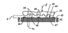
- a mold 36in accordance with the present invention, may be employed in system 10 , and may define a surface having a substantially smooth or planar profile (not shown).
- mold 36may include features defined by a plurality of spaced-apart recessions 38 and protrusions 40 .
- the plurality of featuresdefines an original pattern that forms the basis of a pattern to be formed on a substrate 42 .
- Substrate 42may comprise a bare wafer or a wafer with one or more layers disposed thereon, one of which is shown as primer layer 45 . To that end, reduced is a distance “d” between mold 36 and substrate 42 .
- the features on mold 36may be imprinted into a conformable region of substrate 42 , such as an imprinting material disposed on a portion of surface 44 that presents a substantially planar profile.
- the imprinting materialmay be deposited using any known technique, e.g., spin-coating, dip coating and the like. In the present example, however, the imprinting material is deposited as a plurality of spaced-apart discrete droplets 46 on substrate 42 .
- Imprinting materialis formed from a composition that may be selectively polymerized and cross-linked to record the original pattern therein, defining a recorded pattern.
- the pattern recorded in the imprinting materialis produced, in part, by interaction with mold 36 , e.g., electrical interaction, magnetic interaction, thermal interaction, mechanical interaction or the like.
- mold 36comes into mechanical contact with the imprinting material, spreading droplets 36 , so as to generate a contiguous formation 50 of the imprinting material over surface 44 .
- distance “d”is reduced to allow sub-portions 52 of imprinting material to ingress into and fill recessions 38 .
- the atmosphere between mold 36 and droplets 46is saturated with helium or is completely evacuated or is a partially evacuated atmosphere of helium.
- the imprinting materialis provided with the requisite properties to completely fill recessions 38 while covering surface 44 with a contiguous formation of the imprinting material.
- sub-portions 54 of imprinting material in superimposition with protrusions 40remain after the desired, usually minimum, distance “d” has been reached. This action provides formation 50 with sub-portions 52 having a thickness t 1 , and sub-portions 54 , having a thickness t 2 . Thicknesses “t 1 ” and “t 2 ” may be any thickness desired, dependent upon the application.
- formation 50is solidified by exposing the same to the appropriate curing agent, e.g., actinic energy, such as broadband ultra violet energy, thermal energy or the like, depending upon the imprinting material. This causes the imprinting material to polymerize and cross-link. The entire process may occur at ambient temperatures and pressures, or in an environmentally-controlled chamber with desired temperatures and pressures. In this manner, formation 50 is solidified to provide side 56 thereof with a shape conforming to a shape of a surface 58 of mold 36 .
- actinic energysuch as broadband ultra violet energy, thermal energy or the like
- the characteristics of the imprinting materialare important to efficiently pattern substrate 42 in light of the unique patterning process employed.
- the imprinting materialhave certain characteristics to facilitate rapid and even filling of the features of mold 36 so that all thicknesses t 1 are substantially uniform and all thicknesses t 2 are substantially uniform.
- the viscosity of the imprinting materialbe established, based upon the deposition process employed, to achieve the aforementioned characteristics.
- the imprinting materialmay be deposited on substrate 42 employing various techniques.
- a composition from which the imprinting material is formedhave relatively low viscosity, e.g., in a range of 0.5 to 20 centipoises (cPs).
- cPscentipoises
- the compositionprovides the imprinting material with certain solidified phase characteristics.
- substrate 42may be formed from silicon, plastics, gallium arsenide, mercury telluride, and composites thereof.
- substrate 42may include one or more layers shown as primer layer 45 , e.g., dielectric layer, metal layer, semiconductor layer, planarization layer and the like, upon which formation 50 is generated.
- primer layer 45would be deposited upon a wafer 47 employing any suitable technique, such as chemical vapor deposition, spin-coating and the like.
- primer layer 45may be formed from any suitable material, such as silicon, germanium and the like.
- mold 36may be formed from several materials, e.g., fused-silica, quartz, indium tin oxide diamond-like carbon, MoSi, sol-gels and the like.
- composition from which formation 50 is generatedmay be fabricated from several different families of bulk materials.
- the compositionmay be fabricated from vinyl ethers, methacrylates, epoxies, thiol-enes and acrylates, just to name a few.
- An exemplary bulk material from which to form formation 50is as follows:
- the acrylate componentisobornyl acrylate (IBOA)
- IBOAisobornyl acrylate
- the mechanical properties of formation 50are primarily attributable to IBOA.
- An exemplary source for IBOAis Sartomer Company, Inc. of Exton, Pa. available under the product name SR 506.
- n-hexyl acrylatehas the following structure: and comprises approximately 25% of bulk material by weight, but may be present in a range of 0% to 50%, inclusive. Also providing flexibility to formation 50 , n-HA is employed to reduce the viscosity of the prior art bulk material so that bulk material, in the liquid phase, has a viscosity in a range 2-9 Centipoises, inclusive.
- An exemplary source for the n-HA componentis the Aldrich Chemical Company of Milwaukee, Wis.
- a cross-linking componentethylene glycol diacrylate, has the following structure: and comprises approximately 25% of bulk material by weight, and may be present in a range of 10% to 50%, inclusive.
- EGDAalso contributes to the modulus and stiffness buildup, as well as facilitates cross-linking of n-HA and IBOA during polymerization of the bulk material.
- An initiator component2-hydroxy-2-methyl-1-phenyl-propan-1-one is available from Ciba Specialty Chemicals of Tarrytown, N.Y. under the trade name DAROCUR® 1173, and has the following structure: and comprises approximately 3% of the bulk material by weight, and may be present in a range of 1% to 5%, inclusive.
- the actinic energy to which the initiator is responsiveis broad band ultra-violet energy generated by a medium-pressure mercury lamp. In this manner, the initiator facilitates cross-linking and polymerization of the components of the bulk material.
- composition for the imprinting materialthat includes one of several compositions, such as the BULK IMPRINTING MATERIAL discussed above, along with a component that contains low surface energy groups, referred to as a surfactant component and fully described in U.S. patent application Ser. No. 11/068,171, filed Feb. 28, 2005, entitled “Composition to Reduce Adhesion Between a Conformable Region and a Mold,” having Frank Xu and Michael N. Miller listed as inventors, which is incorporated by reference herein.
- the surfactant componentrises, after a period of time, to the air liquid interface, providing droplets 146 of imprinting material with a bifurcated concentration of materials.
- droplets 146include a higher concentration of the surfactant component, referred to as a surfactant-component-rich (SCR) sub-portion 136 , than the second portion, referred to as a surfactant-component-depleted (SCD) sub-portion 137 .
- SCR sub-rich sub-portion 136a surfactant-component-rich
- SCD sub-portion 137is positioned between surface 44 and SCR sub-portion 136 .
- SCR sub-portion 136attenuates the adhesion forces between mold 36 and the imprinting material, once the imprinting material is solidified.
- the surfactant componenthas opposed ends.
- the imprinting materialis in the liquid phase, i.e., polymerizable, one of the opposed ends has an affinity for the bulk material included in the imprinting material.
- the remaining endhas a fluorine component.
- the surfactant componentis orientated so that the fluorine component extends from an air-liquid interface defined by the imprinting material and the surrounding ambient.
- Lamella 60Upon solidification of the imprinting material, a first portion of the imprinting material generates a lamella 60 and a second portion of the imprinting material is solidified, i.e., polymeric material shown as formation 50 .
- Lamella 60is positioned between formation 50 and mold 36 .
- Lamella 60results from the presence and location of the fluorine components in the SCR sub-portion 136 .
- Lamella 60prevents strong adhesion forces from being developed between mold 36 and formation 50 .
- formation 50has first and second opposed sides 62 and 64 .
- Side 62adheres to mold 36 with a first adhesion force.
- Side 64adheres to substrate 42 with a second adhesion force.
- Lamella 60results in the first adhesion force being less than the second adhesion force.
- mold 36may be easily removed from formation 50 while minimizing distortions and/or the force required to separate mold 36 therefrom.
- formation 50is shown with side 62 being patterned, it should be understood that side
- lamella 60so as to be disposed between formation 50 and substrate 42 .
- Thismay be achieved, for example, by applying imprinting material to mold 36 and subsequently contacting substrate 42 with the imprinting material on mold 36 .
- formation 50will be disposed between lamella 60 and the body, e.g., mold 36 or substrate 42 , upon which the polymerizable material is deposited.
- the imprinting material depositedemploying spin-coating techniques, similar bifurcated concentration of materials occurs, as shown in FIG. 6 with respect to SCR sub-portion 236 and second and SCD sub-portion 237 .
- the time required for the bifurcationis dependent upon several factors, including the size of molecules in the composition and the viscosity of the composition. Only a few seconds is needed to achieve the aforementioned bifurcation of composition with viscosity below twenty cPs. Material with viscosity in the hundreds of cPs, however, may require a few seconds to several minutes.
- lamella 60may not be uniform. Some regions of lamella 60 are thinner than others, and in some extreme cases, lamella 60 may be absent in an extremely small percentage of the template surface so that template 36 is in contact with formation 50 . As a result of the thinner regions of lamella 60 and in the absence of lamella 60 , distortion and/or delamination of formation 50 from substrate 42 may occur. Specifically, upon separation of mold 36 , formation 50 is subjected to a separation force F s . Separation force F s is attributable to a pulling force F p . on mold 36 and adhering forces, e.g., Van der Waals forces, between formation 50 and mold 36 as reduced by lamella 60 .
- separation force F sis attributable to a pulling force F p . on mold 36 and adhering forces, e.g., Van der Waals forces, between formation 50 and mold 36 as reduced by lamella 60 .
- lamella 60 separation force F stypically has a magnitude that is less than the magnitude of an adhering force F A between formation 50 and substrate 42 .
- local separation force F smay approach the magnitude of local adhering force F A .
- local forceswhat is meant are the forces present in a given region of lamella layer 60 , which in this example are the local forces proximate to a thin region of lamella layer 60 or where lamella layer 60 is substantially absent. This leads to distortion and/or delamination of formation 50 from substrate 42 .
- a more complex situationexists due to the presence of two interfaces 66 and 68 .
- a first adhering force F 1is present between primer layer 45 and formation 50 .
- a second adhering force, F 2is present between primer layer 45 and wafer 47 .
- the separation force F shave a magnitude that is less than either adhering forces F 1 and F 2 .
- separation force F smay be similar or approach the magnitude of one or both of adhering forces F 1 and F 2 . This may cause delamination of formation 50 from primer layer 45 , primer layer 45 from wafer 47 or both.
- primer layer 45reduces, if not avoids, the delamination problem mentioned above by forming primer layer 45 from a material that increases the probability that first F 1 and second F 2 adhering forces of the first and second interface, respectively, are greater than the separation force F s in view of lamella layer fluctuations.
- primer layer 45is formed from a composition that forms strong bonds at interface 66 , i.e., between primer layer 45 and formation 50 , as well as, i.e., between interface 66 , primer layer 45 and wafer 47 .
- adhesion between primer layer 45 and formation 50 at first interface 66is the result of covalent bonding, i.e., covalent bonds between the composition from which primer layer 45 is formed and the composition from which formation 50 is formed are present.
- Adhesion between primer layer 45 and wafer 47may be achieved through any one of various mechanisms. These mechanisms may include covalent bonds formed between the composition from which primer layer 45 is formed and the material from which wafer 47 is formed. Alternatively, or in addition to, the covalent bonds, ionic bonds may be formed between the composition from which primer layer 45 is formed and the material from which wafer 47 is formed. Alternatively, or in addition to, the covalent bonds, and/or the ionic bonds or both, adhesion between the composition from which primer layer 45 is formed and the material from which wafer 47 is formed may be achieved vis-à-vis Van der Waals forces.
- primer layer 45from a composition that includes a multi-functional reactive compound, i.e., a compound that contained two or more functional groups generally represented as follows: In which R, R′, R′′ and R′′′ are linking groups and x, y, z are averaged repeating numbers of the groups associated therewith. These repeating units could be randomly distributed.
- the groups X and X′denote the functional groups, with the understanding that typically, the functional group X differs from functional group X′.
- One of the functional groups X and X′, for example X′is selected to achieve cross-reaction with the material from which substrate 42 is formed to adhere thereto by forming a covalent bond therewith, ionic bond therewith and/or Van der Waals forces.
- One of the remaining functional groups X and X′is selected to achieve cross-reaction with the material from which formation 50 is formed to form a covalent bond therebetween.
- the functionality of the X groupis established so the cross-reaction occurs during polymerization of formation 50 .
- the selection of functional group Xdepends upon the characteristics of the material from which formation 50 is formed, it is desired that functional group X reacts with the functional groups of the composition from which formation 50 is formed.
- Xmay be comprised of acrylic, vinyl ether, and or alkoxyl functional groups, and/or functional groups that can copolymerize with acrylic groups in formation 50 .
- X functional groupscross-react in response to ultraviolet actinic energy.
- Functional groups X′may also participate in the cross-linking and polymerization reactions of primer layer 45 .
- X′ functional groupsfacilitate polymerization and cross-linking in response to an actinic energy that differs from the actinic energy in response to which X functional groups cross-react.
- the X′ functional groups in the present examplefacilitate cross-linking of molecules in primer layer 45 in response to exposure to thermal energy.
- functional groups X′are selected to facilitate cross-reaction with substrate 42 through three mechanisms: 1) direct reaction with material from which substrate 42 is formed; 2) reaction with cross-linker molecules with a linking functional group of the cross-linker reacting with substrate 42 ; and 3) polymerization of and cross-linking of primer layer 45 so that chains of molecules of sufficient length may be developed to connected between formation 50 and substrate 42 .
- an exemplary multi-functional reactive compound that may be employed to form primer layer 45 in the presence of formation 50 being formed from BULK MATERIALincludes a ⁇ -carboxyethyl acrylate, available from UCB Chemicals in Smyrna, Ga. under the product name ⁇ -CEA.
- ⁇ -CEAis an aliphatic compound having the following structure:
- the X′ functional group 70provides carboxylic functionality.
- the X functional group 72provides acrylate functionality.
- Functional groups 70 and 72are coupled to opposing ends of a backbone component 74 .
- another multi-functional reactive compound that may be employed to form primer layer 45 in the presence of formation 50 being formed from BULK MATERIALincludes an aromatic bis-phenyl compound available from UCB Chemicals in Smyrna, Ga. under the product name Ebecryl 3605 that has the following structure:
- the X′ functional group 76provides epoxy functionality.
- the X functional group 78provides acrylate functionality.
- Functional groups 76 and 78are coupled to opposing ends of a backbone component 80 .
- another multi-functional reactive compound that may be employed to form primer layer 45 in the presence of formation 50 being formed from BULK MATERIALincludes an aromatic compound available from Schenectady International, Inc. in Schenectady, N.Y. under the product name Isorad 501 that has the following structure: where x and y are integers indicating repeating units that are randomly distributed.
- the X′ functional group 82provides carboxylic functionality.
- the X functional group 84provides acrylate functionality. Functional groups 82 and 84 are coupled to opposing ends of a backbone component 86 .
- functional group Xmay generate radicals that function to facilitate polymerization of the composition from which formation 50 is formed during solidification of the same.
- the functional group Xwould facilitate polymerization of formation 50 upon exposure to actinic energy, e.g., broad band ultraviolet energy.
- An exemplary multi-functional reactive compound that includes these propertiesis a photo-initiator available from Ciba Specialty Chemicals in Tarrytown, N.Y. under the tradename Irgacure 2959 and has the following structure:
- the X′ functional group 90provides hydroxyl functionality.
- the X functional group 92provides initiator-type functionality.
- the functional group Xundergoes alpha-cleavage to generate benzoyl type of radicals.
- the radicalsfacilitate radical polymerization of the composition from which formation 50 is formed.
- Functional groups 90 and 92are coupled to opposing ends of a backbone component 94 .
- compositionswere formed including some of the aforementioned the multi-functional reactive compounds to determine the adhering strength of interfaces 66 and 68 .
- An exemplary composition including a multi-functional reactive compoundis as follows:
- DUV30J-16comprises approximately 100 grams of composition 1 and ⁇ -CEA comprises approximately 0.219 grams.
- DUV30J-16is a bottom anti-reflective coating, BARC, available from Brewer Science in Rolla, Mo. containing 93% solvent, and 7% non-solvent reactive components.
- BARCbottom anti-reflective coating
- DUV30J-16contains phenolic resins, and its crosslinker can react with carboxylic functional group. It is believed that DUV30J-16 will not form covalent bonds with formation 50 .
- ⁇ -CEAwas replaced by a cross-linking agent, a catalyst and IsoRad 501. Both the cross-linking agent and catalyst is sold by Cytec Industries, Inc. of West Patterson, N.J.
- the cross-linking agentis sold under the product name Cymel 303ULF.
- Cymel 303ULFOne of the main components of Cymel 303ULF is hexamethoxymethyl-melamine (HMMM).
- HMMMhexamethoxymethyl-melamine
- the methoxyl functional groups of HMMMcan participate in many condensation reactions.
- the catalystis sold under the product name Cycat 4040 providing the following composition:
- COMPOSITION 2comprises DUV30J-16
- 0.611 gram of COMPOSITION 2comprises IsoRad 501
- 0.175 gram of COMPOSITION 2comprises Cymel 303ULF
- 0.008 gram of COMPOSITION 2comprises Cycat 4040.
- compositionthat may be employed as the multi-functional reactive compound omits DUV30J-16.
- the compositionis as follows:
- PM Acetate Composition 3includes approximately 77 grams of IsoRad 501, 22 grams of Cymel 303ULF and one gram of Cycat 4040. IsoRad 501, Cymel 303ULF and Cycat are combined. The combination of IsoRad 501, Cymel 303ULF and Cycat are then introduced into approximately 1900 grams of PM Acetate.
- PM Acetateis a product name of a solvent consisting of 2-(1-Methoxy)propyl acetate sold by Eastman Chemical Company of Kingsport, Tenn.
- a fourth compositionis identical to COMPOSITION 3, excepting for the amount of the constituent components included.
- COMPOSITION 4includes approximately 85.2 grams of IsoRad 501, 13.8 grams of Cymel 303ULF and one gram of Cycat 4040. IsoRad 501, Cymel 303ULF and Cycat are combined. The combination of IsoRad 501, Cymel 303ULF and Cycat are then introduced into approximately 1900 grams of PM Acetate.
- a fifth compositionis identical to COMPOSITION 3, excepting for the amount of the constituent components included.
- COMPOSITION 5includes approximately 81 grams of IsoRad 501, 18 grams of Cymel 303ULF and one gram of Cycat 4040. IsoRad 501, Cymel 303ULF and Cycat are combined. The combination of IsoRad 501, Cymel 303ULF and Cycat are then introduced into approximately 1900 grams of PM Acetate.
- compositions discussed above with respect to primer layer 45 , , COMPOSITIONs 1-5are deposited upon substrate 42 employing spin-coating techniques wherein the substrate is rotated at a velocity between 500 and 4,000 revolutions per minute so as to provide a substantially smooth, if not planar layer with uniform thickness. This is followed by exposing the compositions to thermal actinic energy of 180° C. (Celsius) for approximately two minutes.
- compositions described above, COMPOSITIONs 1-5were employed, along with IMPRINTING MATERIAL, to generate comparative data of the strength of the adhesion forces of interfaces 66 and 68 which was compared against baseline measuring of a primer layer 45 formed entirely from DUV30J-16, which is not known to form covalent bonds with formation 50 formed from IMPRINTING MATERIAL.
- formation 50formed from BULK IMPRINTING MATERIAL
- primer layer 45formed from COMPOSITIONS 1-5 and the base line COMPOSITION, were deposited and then solidified between two glass slides (not shown). Each glass slide (not shown) is approximately 1 mm thick, 75 ⁇ 25 mm in the lateral dimension.
- the glass slides (not shown)are subsequently rinsed with de-ionized water, sprayed with isopropyl alcohol, and exposed to a stream of fluid for drying, e.g., a stream of nitrogen gas. Thereafter, the glass slides (not shown) are baked at 120° C. (Celsius) for 2 hours.
- Primer layer 45is deposited onto each of the two glass slides (not shown) employing spin-on techniques with a spin speed up to 3000 rpm. Primer layer 45 is lying on the glass slides (not shown) on hot plates at 180C. for 2 minutes.
- each of COMPOSITIONs 1-5, as well as the baseline compositionare solidified, i.e., polymerized and cross-linked, by exposure to thermal energy. Formation is formed employing drop dispense techniques mentioned above. Specifically, BULK IMPRINTING MATERIAL is disposed as a plurality of droplets onto primer layer 45 on one of the two glass slides.
- the BULK IMPRINTING MATERIALis then sandwiched between two primer layers 45 by having the primer layer on the two glass slides (not shown) facing one another and contacting BULK IMPRINTING MATERIAL.
- a longitudinal axis of one of the two glass slides (not shown)extends orthogonally to the longitudinal axis of the remaining glass slide (not shown).
- the BULK IMPRINTING MATERIALis solidified, i.e., polymerized, and cross-linked by exposing the two glass slides (not shown) to actinic energy, such as broad band ultraviolet wavelengths, using a medium pressure mercury UV lamp for 40 seconds at 20 mW/cm2 intensity.
- the solvent PM Acetateis employed primarily to dissolve the other constituent components of COMPOSITIONs 3, 4 and 5.
- many common photo-resist solventsmay be employed in lieu of PM Acetate, such as Diethylene Glycol Monoethyl Ether Acetate, Methyl Amyl Ketone or the like.
- the solid contents of COMPOSITIONs 3, 4 and 5, i.e., IsoRad 501, Cymel 303ULF and Cycatmay comprise between 0.1% to 70% of the composition, weight, and more preferably in a range of 0.5% to 10% by weight, with the remaining quantity consisting of the solvent.
- the solid component of each of COMPOSITIONs 3, 4, and 5may comprise 50% to 99%, by weight of IsoRad 501, 1% to 50%, by weight of Cymel 303ULF and 0% to 10% by weight of Cycat 4040.
Landscapes
- Chemical & Material Sciences (AREA)
- Engineering & Computer Science (AREA)
- Nanotechnology (AREA)
- Organic Chemistry (AREA)
- Crystallography & Structural Chemistry (AREA)
- Physics & Mathematics (AREA)
- Manufacturing & Machinery (AREA)
- General Physics & Mathematics (AREA)
- Chemical Kinetics & Catalysis (AREA)
- Polymers & Plastics (AREA)
- Condensed Matter Physics & Semiconductors (AREA)
- Health & Medical Sciences (AREA)
- Metallurgy (AREA)
- Microelectronics & Electronic Packaging (AREA)
- Materials Engineering (AREA)
- Mathematical Physics (AREA)
- Theoretical Computer Science (AREA)
- Medicinal Chemistry (AREA)
- Mechanical Engineering (AREA)
- General Chemical & Material Sciences (AREA)
- Adhesives Or Adhesive Processes (AREA)
- Shaping Of Tube Ends By Bending Or Straightening (AREA)
- Exposure Of Semiconductors, Excluding Electron Or Ion Beam Exposure (AREA)
- Addition Polymer Or Copolymer, Post-Treatments, Or Chemical Modifications (AREA)
- Macromonomer-Based Addition Polymer (AREA)
- Laminated Bodies (AREA)
Abstract
Description
- The present application is a divisional of U.S. patent application Ser. No. ______ (Attorney Docket No. P235N226D226 filed herewith, entitled “Composition for Adhering Materials Together,” listing Frank Y. Xu as inventor, which is incorporated by reference herein.
- The United States government has a paid-up license in this invention and the right in limited circumstance to require the patent owner to license others on reasonable terms as provided by the terms of 70NANB4H3012 awarded by National Institute of Standards (NIST) ATP Award.
- The field of invention relates generally to nano-fabrication of structures. More particularly, the present invention is directed to a method for adhering differing materials together suitable for use in imprint lithographic processes.
- Nano-scale fabrication involves the fabrication of very small structures, e.g., having features on the order of one nanometer or more. A promising process for use in nano-scale fabrication is known as imprint lithography. Exemplary imprint lithography processes are described in detail in numerous publications, such as United States published patent application 2004-0065976 filed as U.S. patent application Ser. No. 10/264,960, entitled “Method and a Mold to Arrange Features on a Substrate to Replicate Features having Minimal Dimensional Variability”; United States published patent application 2004-0065252 filed as U.S. patent application Ser. No. 10/264,926, entitled “Method of Forming a Layer on a Substrate to Facilitate Fabrication of Metrology Standards”; and United States published patent application 2004-0046271 filed as U.S. patent application Ser. No. 10/235,314, entitled “Method and a Mold to Arrange Features on a Substrate to Replicate Features having Minimal Dimensions Variability”; all of which are assigned to the assignee of the present invention.
- Referring to
FIG. 1 , the basic concept behind imprint lithography is forming a relief pattern on a substrate that may function as, inter alia, an etching mask so that a pattern may be formed into the substrate that corresponds to the relief pattern. Asystem 10 employed to form the relief pattern includes astage 11 upon which asubstrate 12 is supported, and atemplate 14 having amold 16 with apatterning surface 18 thereon. Patterningsurface 18 may be substantially smooth and/or planar, or may be patterned so that one or more recesses are formed therein.Template 14 is coupled to animprint head 20 to facilitate movement oftemplate 14. Afluid dispense system 22 is coupled to be selectively placed in fluid communication withsubstrate 12 so as to depositpolymerizable material 24 thereon. Asource 26 ofenergy 28 is coupled todirect energy 28 along apath 30.Imprint head 20 andstage 11 are configured to arrangemold 16 andsubstrate 12, respectively, to be in superimposition, and disposed inpath 30. Eitherimprint head 20,stage 11, or both vary a distance betweenmold 16 andsubstrate 12 to define a desired volume therebetween that is filled bypolymerizable material 24. - Typically,
polymerizable material 24 is disposed uponsubstrate 12 before the desired volume is defined betweenmold 16 andsubstrate 12. However,polymerizable material 24 may fill the volume after the desired volume has been obtained. After the desired volume is filled withpolymerizable material 24,source 26 producesenergy 28, which causespolymerizable material 24 to solidify and/or cross-link, forming polymeric material conforming to the shape of thesubstrate surface 25 andmold surface 18. Control of this process is regulated byprocessor 32 that is in data communication withstage 11imprint head 20,fluid dispense system 22, andsource 26, operating on a computer-readable program stored inmemory 34. - An important characteristic with accurately forming the pattern in the polymerizable material is to reduce, if not prevent, adhesion to the mold of the polymeric material, while ensuring suitable adhesion to the substrate. This is referred to as preferential release and adhesion properties. In this manner, the pattern recorded in the polymeric material is not distorted during separation of the mold. Prior art attempts to improve the release characteristics employ a release layer on the surface of the mold. The release layer is typically hydrophobic and/or has low surface energy. The release layer adheres to the mold. Providing the release layer improves release characteristics. This is seen by minimization of distortions in the pattern recorded into the polymeric material that are attributable to mold separation. This type of release layer is referred to, for purposes of the present discussion, as an a priori release layer, i.e., a release layer that is solidified to the mold.
- Another prior art attempt to improve release properties is described by Bender et al. in “Multiple Imprinting in UV-based Nanoimprint Lithography: Related Material Issues,” Microeletronic Engineering 61-62 (2002), pp. 407-413. Specifically, Bender et al. employ a mold having an a priori release layer in conjunction with a fluorine-treated UV curable material. To that end, a UV curable layer is applied to a substrate by spin-coating a 200 cPs UV curable fluid to form a UV curable layer. The UV curable layer is enriched with fluorine groups to improve the release properties.
- A need exists, therefore, to improve the preferential release and adhesion properties of a mold employed in imprint lithography processes.
- The present invention provides a method of adhering a layer to a substrate that features defining first and second interfaces by having a composition present between the layer and the substrate that forms covalent bonds to the layer and adheres to the substrate employing one or more of covalent bonds, ionic bonds and Van der Waals forces. In this manner, the strength of the adhering force of the layer to the composition is assured to be stronger than the adhering force of the layer to the composition having a predetermined adhering mechanism, i.e., an adhering mechanism that does not include covalent bonding. These and other embodiments are described herein.
FIG. 1 is a simplified plan view of a lithographic system in accordance with the prior art;FIG. 2 is a simplified elevation view of a template and imprinting material disposed on a substrate in accordance with the present invention;FIG. 3 is a simplified elevation view of the template and substrate, shown inFIG. 2 , with the imprinting material being shown as patterned and solidified upon the layer;FIG. 4 is a cross-sectional view of the template contacting imprinting material demonstrating the formation of the weak boundary lamella between solidified imprinting material and a template;FIG. 5 is a detailed view of the droplets of imprint material, shown inFIG. 2 , showing the bifurcation of the droplets into surfactant-rich regions and surfactant-depleted regions;FIG. 6 is a detailed view of a layer of imprinting material, deposited employing spin-on techniques, showing the bifurcation of the layer into surfactant-rich regions and surfactant-depleted regions;FIG. 7 is a cross-sectional view of the template contacting solidified imprinting material, deposited as shown in either FIGS.5 or6, formed on a substrate including a primer layer;FIG. 8 is a plan view showing the chemical structure of a component of a composition that may be employed to form the primer layer shown inFIGS. 2, 3 , and7, in accordance with one embodiment of the present invention;FIG. 9 is a plan view showing the chemical structure of a component of a composition that may be employed to form the primer layer shown inFIGS. 2, 3 , and7, in accordance with a second embodiment of the present invention;FIG. 10 is a plan view showing the chemical structure of a component of a composition that may be employed to form the primer layer shown inFIGS. 2, 3 , and7, in accordance with a third embodiment of the present invention; andFIG. 11 is a plan view showing the chemical structure of a component of a composition that may be employed to form the primer layer shown inFIGS. 2, 3 , and7, in accordance with a fourth embodiment of the present invention.- Referring to
FIGS. 1 and 2 , amold 36, in accordance with the present invention, may be employed insystem 10, and may define a surface having a substantially smooth or planar profile (not shown). Alternatively,mold 36 may include features defined by a plurality of spaced-apart recessions 38 andprotrusions 40. The plurality of features defines an original pattern that forms the basis of a pattern to be formed on asubstrate 42.Substrate 42 may comprise a bare wafer or a wafer with one or more layers disposed thereon, one of which is shown asprimer layer 45. To that end, reduced is a distance “d” betweenmold 36 andsubstrate 42. In this manner, the features onmold 36 may be imprinted into a conformable region ofsubstrate 42, such as an imprinting material disposed on a portion ofsurface 44 that presents a substantially planar profile. It should be understood that the imprinting material may be deposited using any known technique, e.g., spin-coating, dip coating and the like. In the present example, however, the imprinting material is deposited as a plurality of spaced-apartdiscrete droplets 46 onsubstrate 42. Imprinting material is formed from a composition that may be selectively polymerized and cross-linked to record the original pattern therein, defining a recorded pattern. - Specifically, the pattern recorded in the imprinting material is produced, in part, by interaction with
mold 36, e.g., electrical interaction, magnetic interaction, thermal interaction, mechanical interaction or the like. In the present example,mold 36 comes into mechanical contact with the imprinting material, spreadingdroplets 36, so as to generate acontiguous formation 50 of the imprinting material oversurface 44. In one embodiment, distance “d” is reduced to allowsub-portions 52 of imprinting material to ingress into and fillrecessions 38. To facilitate filling ofrecessions 38, before contact betweenmold 36 anddroplets 46, the atmosphere betweenmold 36 anddroplets 46 is saturated with helium or is completely evacuated or is a partially evacuated atmosphere of helium. - The imprinting material is provided with the requisite properties to completely fill
recessions 38 while coveringsurface 44 with a contiguous formation of the imprinting material. In the present embodiment, sub-portions54 of imprinting material in superimposition withprotrusions 40 remain after the desired, usually minimum, distance “d” has been reached. This action providesformation 50 withsub-portions 52 having a thickness t1, and sub-portions54, having a thickness t2. Thicknesses “t1” and “t2” may be any thickness desired, dependent upon the application. Thereafter,formation 50 is solidified by exposing the same to the appropriate curing agent, e.g., actinic energy, such as broadband ultra violet energy, thermal energy or the like, depending upon the imprinting material. This causes the imprinting material to polymerize and cross-link. The entire process may occur at ambient temperatures and pressures, or in an environmentally-controlled chamber with desired temperatures and pressures. In this manner,formation 50 is solidified to provideside 56 thereof with a shape conforming to a shape of asurface 58 ofmold 36. - Referring to
FIGS. 1, 2 and3, the characteristics of the imprinting material are important to efficientlypattern substrate 42 in light of the unique patterning process employed. For example, it is desired that the imprinting material have certain characteristics to facilitate rapid and even filling of the features ofmold 36 so that all thicknesses t1are substantially uniform and all thicknesses t2are substantially uniform. To that end, it is desirable that the viscosity of the imprinting material be established, based upon the deposition process employed, to achieve the aforementioned characteristics. As mentioned above, the imprinting material may be deposited onsubstrate 42 employing various techniques. Were the imprinting material deposited as a plurality of discrete and spaced-apartdroplets 46, it would be desirable that a composition from which the imprinting material is formed have relatively low viscosity, e.g., in a range of 0.5 to 20 centipoises (cPs). Considering that the imprinting material is spread and patterned concurrently, with the pattern being subsequently solidified intoformation 50 by exposure to radiation, it would be desired to have the composition wet surface ofsubstrate 42 and/ormold 36 and to avoid subsequent pit or hole formation after polymerization. Were the imprinting material deposited employing spin-coating techniques, it would be desired to use higher viscosity materials, e.g., having a viscosity greater than 10 cPs and typically, several hundred to several thousand cPs, with the viscosity measurement being determined in the absence of a solvent. - In addition to the aforementioned characteristics, referred to as liquid phase characteristics, it is desirable that the composition provides the imprinting material with certain solidified phase characteristics. For example, after solidification of
formation 50, it is desirable that preferential adhesion and release characteristics be demonstrated by the imprinting material. Specifically, it is beneficial for the composition from which the imprinting material is fabricated to provideformation 50 with preferential adhesion tosubstrate 42 and preferential release ofmold 36. In this fashion, reduced is the probability of distortions in the recorded pattern resulting from the separation ofmold 36 therefrom due to, inter alia, tearing, stretching or other structural degradation offormation 50. - The constituent components of the composition that form the imprinting material to provide the aforementioned characteristics may differ. This results from
substrate 42 being formed from a number of different materials. As a result, the chemical composition ofsurface 44 varies dependent upon the material from whichsubstrate 42 is formed. For example,substrate 42 may be formed from silicon, plastics, gallium arsenide, mercury telluride, and composites thereof. As mentioned above,substrate 42 may include one or more layers shown asprimer layer 45, e.g., dielectric layer, metal layer, semiconductor layer, planarization layer and the like, upon whichformation 50 is generated. To that end,primer layer 45 would be deposited upon awafer 47 employing any suitable technique, such as chemical vapor deposition, spin-coating and the like. Additionally,primer layer 45 may be formed from any suitable material, such as silicon, germanium and the like. Additionally,mold 36 may be formed from several materials, e.g., fused-silica, quartz, indium tin oxide diamond-like carbon, MoSi, sol-gels and the like. - It has been found that the composition from which
formation 50 is generated may be fabricated from several different families of bulk materials. For example, the composition may be fabricated from vinyl ethers, methacrylates, epoxies, thiol-enes and acrylates, just to name a few. - An exemplary bulk material from which to form
formation 50 is as follows: - The acrylate component, isobornyl acrylate (IBOA), has the following structure:

and comprises approximately 47% of bulk material by weight, but may be present in a range of 20% to 80%, inclusive. As a result, the mechanical properties offormation 50 are primarily attributable to IBOA. An exemplary source for IBOA is Sartomer Company, Inc. of Exton, Pa. available under the product name SR 506. - The component n-hexyl acrylate (n-HA) has the following structure:

and comprises approximately 25% of bulk material by weight, but may be present in a range of 0% to 50%, inclusive. Also providing flexibility toformation 50, n-HA is employed to reduce the viscosity of the prior art bulk material so that bulk material, in the liquid phase, has a viscosity in a range 2-9 Centipoises, inclusive. An exemplary source for the n-HA component is the Aldrich Chemical Company of Milwaukee, Wis. - A cross-linking component, ethylene glycol diacrylate, has the following structure:

and comprises approximately 25% of bulk material by weight, and may be present in a range of 10% to 50%, inclusive. EGDA also contributes to the modulus and stiffness buildup, as well as facilitates cross-linking of n-HA and IBOA during polymerization of the bulk material. - An initiator component, 2-hydroxy-2-methyl-1-phenyl-propan-1-one is available from Ciba Specialty Chemicals of Tarrytown, N.Y. under the trade name DAROCUR® 1173, and has the following structure:

and comprises approximately 3% of the bulk material by weight, and may be present in a range of 1% to 5%, inclusive. The actinic energy to which the initiator is responsive is broad band ultra-violet energy generated by a medium-pressure mercury lamp. In this manner, the initiator facilitates cross-linking and polymerization of the components of the bulk material. - It has been disclosed, however, in co-pending U.S. patent application Ser. No. 11/068,171, filed Feb. 28, 2005, entitled “Composition to Reduce Adhesion Between a Conformable Region and a Mold,” having Frank Xu and Michael N. Miller listed as inventors, that desirable preferential adhesion and release properties, as discussed above, may be achieved by producing a weak boundary layer,
lamella 60, betweenmold 36,surface 58 andformation 50, shown inFIGS. 3 and 4 .Lamella 60 remains after solidification of the imprinting material. As a result, the adhesion forced betweenmold 36 andformation 50 are minimal. To that end, found beneficial was employing a composition for the imprinting material that includes one of several compositions, such as the BULK IMPRINTING MATERIAL discussed above, along with a component that contains low surface energy groups, referred to as a surfactant component and fully described in U.S. patent application Ser. No. 11/068,171, filed Feb. 28, 2005, entitled “Composition to Reduce Adhesion Between a Conformable Region and a Mold,” having Frank Xu and Michael N. Miller listed as inventors, which is incorporated by reference herein. - Referring to
FIG. 5 , after deposition of the imprinting material, the surfactant component rises, after a period of time, to the air liquid interface, providingdroplets 146 of imprinting material with a bifurcated concentration of materials. In a first portion,droplets 146 include a higher concentration of the surfactant component, referred to as a surfactant-component-rich (SCR) sub-portion136, than the second portion, referred to as a surfactant-component-depleted (SCD) sub-portion137. SCD sub-portion137 is positioned betweensurface 44 andSCR sub-portion 136. SCR sub-portion136 attenuates the adhesion forces betweenmold 36 and the imprinting material, once the imprinting material is solidified. Specifically, the surfactant component has opposed ends. When the imprinting material is in the liquid phase, i.e., polymerizable, one of the opposed ends has an affinity for the bulk material included in the imprinting material. The remaining end has a fluorine component. - Referring to
FIGS. 4 and 5 , as a result of the affinity for the bulk material, the surfactant component is orientated so that the fluorine component extends from an air-liquid interface defined by the imprinting material and the surrounding ambient. - Upon solidification of the imprinting material, a first portion of the imprinting material generates a
lamella 60 and a second portion of the imprinting material is solidified, i.e., polymeric material shown asformation 50.Lamella 60 is positioned betweenformation 50 andmold 36.Lamella 60 results from the presence and location of the fluorine components in theSCR sub-portion 136.Lamella 60 prevents strong adhesion forces from being developed betweenmold 36 andformation 50. Specifically,formation 50 has first and secondopposed sides Side 62 adheres to mold36 with a first adhesion force.Side 64 adheres tosubstrate 42 with a second adhesion force.Lamella 60 results in the first adhesion force being less than the second adhesion force. As a result,mold 36 may be easily removed fromformation 50 while minimizing distortions and/or the force required to separatemold 36 therefrom. Althoughformation 50 is shown withside 62 being patterned, it should be understood thatside 62 may be smooth, if not planar. - Furthermore, if desired, it is possible to generate
lamella 60 so as to be disposed betweenformation 50 andsubstrate 42. This may be achieved, for example, by applying imprinting material to mold36 and subsequently contactingsubstrate 42 with the imprinting material onmold 36. In this manner, it can be said thatformation 50 will be disposed betweenlamella 60 and the body, e.g.,mold 36 orsubstrate 42, upon which the polymerizable material is deposited. It should be understood that were the imprinting material deposited employing spin-coating techniques, similar bifurcated concentration of materials occurs, as shown inFIG. 6 with respect toSCR sub-portion 236 and second andSCD sub-portion 237. The time required for the bifurcation is dependent upon several factors, including the size of molecules in the composition and the viscosity of the composition. Only a few seconds is needed to achieve the aforementioned bifurcation of composition with viscosity below twenty cPs. Material with viscosity in the hundreds of cPs, however, may require a few seconds to several minutes. - It has been discovered, however, that
lamella 60 may not be uniform. Some regions oflamella 60 are thinner than others, and in some extreme cases,lamella 60 may be absent in an extremely small percentage of the template surface so thattemplate 36 is in contact withformation 50. As a result of the thinner regions oflamella 60 and in the absence oflamella 60, distortion and/or delamination offormation 50 fromsubstrate 42 may occur. Specifically, upon separation ofmold 36,formation 50 is subjected to a separation force Fs. Separation force Fsis attributable to a pulling force Fp. onmold 36 and adhering forces, e.g., Van der Waals forces, betweenformation 50 andmold 36 as reduced bylamella 60. Due to the presence oflamella 60 separation force Fstypically has a magnitude that is less than the magnitude of an adhering force FAbetweenformation 50 andsubstrate 42. However, with the reduction, or absence, oflamella 60, local separation force Fsmay approach the magnitude of local adhering force FA. By local forces what is meant are the forces present in a given region oflamella layer 60, which in this example are the local forces proximate to a thin region oflamella layer 60 or wherelamella layer 60 is substantially absent. This leads to distortion and/or delamination offormation 50 fromsubstrate 42. - Referring to
FIG. 7 , in the presence ofprimer layer 45, a more complex situation exists due to the presence of twointerfaces primer layer 45 andformation 50. At a second interface68 a second adhering force, F2, is present betweenprimer layer 45 andwafer 47. It is desired that the separation force Fshave a magnitude that is less than either adhering forces F1and F2. However, due to variations in the thickness, or absence, oflamella 60, as discussed above, separation force Fsmay be similar or approach the magnitude of one or both of adhering forces F1and F2. This may cause delamination offormation 50 fromprimer layer 45,primer layer 45 fromwafer 47 or both. - The present invention reduces, if not avoids, the delamination problem mentioned above by forming
primer layer 45 from a material that increases the probability that first F1and second F2adhering forces of the first and second interface, respectively, are greater than the separation force Fsin view of lamella layer fluctuations. To that end,primer layer 45 is formed from a composition that forms strong bonds atinterface 66, i.e., betweenprimer layer 45 andformation 50, as well as, i.e., betweeninterface 66,primer layer 45 andwafer 47. In the present example, adhesion betweenprimer layer 45 andformation 50 atfirst interface 66 is the result of covalent bonding, i.e., covalent bonds between the composition from whichprimer layer 45 is formed and the composition from whichformation 50 is formed are present. Adhesion betweenprimer layer 45 andwafer 47 may be achieved through any one of various mechanisms. These mechanisms may include covalent bonds formed between the composition from whichprimer layer 45 is formed and the material from whichwafer 47 is formed. Alternatively, or in addition to, the covalent bonds, ionic bonds may be formed between the composition from whichprimer layer 45 is formed and the material from whichwafer 47 is formed. Alternatively, or in addition to, the covalent bonds, and/or the ionic bonds or both, adhesion between the composition from whichprimer layer 45 is formed and the material from whichwafer 47 is formed may be achieved vis-à-vis Van der Waals forces. - This is achieved by forming primer layer45 from a composition that includes a multi-functional reactive compound, i.e., a compound that contained two or more functional groups generally represented as follows:

In which R, R′, R″ and R′″ are linking groups and x, y, z are averaged repeating numbers of the groups associated therewith. These repeating units could be randomly distributed. The groups X and X′ denote the functional groups, with the understanding that typically, the functional group X differs from functional group X′. One of the functional groups X and X′, for example X′, is selected to achieve cross-reaction with the material from whichsubstrate 42 is formed to adhere thereto by forming a covalent bond therewith, ionic bond therewith and/or Van der Waals forces. - One of the remaining functional groups X and X′, for example X, is selected to achieve cross-reaction with the material from which
formation 50 is formed to form a covalent bond therebetween. The functionality of the X group is established so the cross-reaction occurs during polymerization offormation 50. As a result, the selection of functional group X depends upon the characteristics of the material from whichformation 50 is formed, it is desired that functional group X reacts with the functional groups of the composition from whichformation 50 is formed. For example, wereformation 50 formed from acrylate monomers, X may be comprised of acrylic, vinyl ether, and or alkoxyl functional groups, and/or functional groups that can copolymerize with acrylic groups information 50. As a result, X functional groups cross-react in response to ultraviolet actinic energy. - Functional groups X′ may also participate in the cross-linking and polymerization reactions of
primer layer 45. Typically, X′ functional groups facilitate polymerization and cross-linking in response to an actinic energy that differs from the actinic energy in response to which X functional groups cross-react. The X′ functional groups in the present example facilitate cross-linking of molecules inprimer layer 45 in response to exposure to thermal energy. Typically, functional groups X′ are selected to facilitate cross-reaction withsubstrate 42 through three mechanisms: 1) direct reaction with material from whichsubstrate 42 is formed; 2) reaction with cross-linker molecules with a linking functional group of the cross-linker reacting withsubstrate 42; and 3) polymerization of and cross-linking ofprimer layer 45 so that chains of molecules of sufficient length may be developed to connected betweenformation 50 andsubstrate 42. - Referring to
FIGS. 7 and 8 , an exemplary multi-functional reactive compound that may be employed to form primer layer45 in the presence of formation50 being formed from BULK MATERIAL includes a β-carboxyethyl acrylate, available from UCB Chemicals in Smyrna, Ga. under the product name β-CEA. β-CEA is an aliphatic compound having the following structure:
The X′functional group 70 provides carboxylic functionality. The Xfunctional group 72 provides acrylate functionality.Functional groups backbone component 74. - Referring to
FIGS. 7 and 9 , another multi-functional reactive compound that may be employed to form primer layer45 in the presence of formation50 being formed from BULK MATERIAL includes an aromatic bis-phenyl compound available from UCB Chemicals in Smyrna, Ga. under the product name Ebecryl 3605 that has the following structure:
The X′functional group 76 provides epoxy functionality. The Xfunctional group 78 provides acrylate functionality.Functional groups backbone component 80. - Referring to
FIGS. 7 and 10 , another multi-functional reactive compound that may be employed to form primer layer45 in the presence of formation50 being formed from BULK MATERIAL includes an aromatic compound available from Schenectady International, Inc. in Schenectady, N.Y. under the product name Isorad 501 that has the following structure:
where x and y are integers indicating repeating units that are randomly distributed. The X′functional group 82 provides carboxylic functionality. The Xfunctional group 84 provides acrylate functionality.Functional groups backbone component 86. - Referring to
FIGS. 7 and 11 , in addition to cross-reaction with formation50, functional group X may generate radicals that function to facilitate polymerization of the composition from which formation50 is formed during solidification of the same. As a result, the functional group X would facilitate polymerization of formation50 upon exposure to actinic energy, e.g., broad band ultraviolet energy. An exemplary multi-functional reactive compound that includes these properties is a photo-initiator available from Ciba Specialty Chemicals in Tarrytown, N.Y. under the tradename Irgacure 2959 and has the following structure:
The X′functional group 90 provides hydroxyl functionality. The Xfunctional group 92 provides initiator-type functionality. Specifically, in response to exposure to broad band ultraviolet energy the functional group X undergoes alpha-cleavage to generate benzoyl type of radicals. The radicals facilitate radical polymerization of the composition from whichformation 50 is formed.Functional groups backbone component 94. - Several compositions were formed including some of the aforementioned the multi-functional reactive compounds to determine the adhering strength of
interfaces - Composition 1
- β-CEA
- DUV30J-16
- where DUV30J-16 comprises approximately 100 grams of composition 1 and β-CEA comprises approximately 0.219 grams. DUV30J-16 is a bottom anti-reflective coating, BARC, available from Brewer Science in Rolla, Mo. containing 93% solvent, and 7% non-solvent reactive components. DUV30J-16 contains phenolic resins, and its crosslinker can react with carboxylic functional group. It is believed that DUV30J-16 will not form covalent bonds with
formation 50. In another composition, β-CEA was replaced by a cross-linking agent, a catalyst and IsoRad 501. Both the cross-linking agent and catalyst is sold by Cytec Industries, Inc. of West Patterson, N.J. The cross-linking agent is sold under the product name Cymel 303ULF. One of the main components of Cymel 303ULF is hexamethoxymethyl-melamine (HMMM). The methoxyl functional groups of HMMM can participate in many condensation reactions. The catalyst is sold under the product name Cycat 4040 providing the following composition: - Composition 2
- DUV30J-16
- Isorad 501
- Cymel 303ULF
- Cycat 4040
- Approximately 100 grams of COMPOSITION 2 comprises DUV30J-16, 0.611 gram of COMPOSITION 2 comprises IsoRad 501, 0.175 gram of COMPOSITION 2 comprises Cymel 303ULF and 0.008 gram of COMPOSITION 2 comprises Cycat 4040.
- Another composition that may be employed as the multi-functional reactive compound omits DUV30J-16. The composition is as follows:
- Composition 3
- IsoRad 501
- Cymel 303ULF
- Cycat
- PM Acetate Composition 3 includes approximately 77 grams of
IsoRad 501, 22 grams of Cymel 303ULF and one gram of Cycat 4040. IsoRad 501, Cymel 303ULF and Cycat are combined. The combination of IsoRad 501, Cymel 303ULF and Cycat are then introduced into approximately 1900 grams of PM Acetate. PM Acetate is a product name of a solvent consisting of 2-(1-Methoxy)propyl acetate sold by Eastman Chemical Company of Kingsport, Tenn. - A fourth composition is identical to COMPOSITION 3, excepting for the amount of the constituent components included. For example, COMPOSITION 4 includes approximately 85.2 grams of IsoRad 501, 13.8 grams of Cymel 303ULF and one gram of Cycat 4040. IsoRad 501, Cymel 303ULF and Cycat are combined. The combination of IsoRad 501, Cymel 303ULF and Cycat are then introduced into approximately 1900 grams of PM Acetate.
- A fifth composition is identical to COMPOSITION 3, excepting for the amount of the constituent components included. For example, COMPOSITION 5 includes approximately 81 grams of
IsoRad 501, 18 grams of Cymel 303ULF and one gram of Cycat 4040. IsoRad 501, Cymel 303ULF and Cycat are combined. The combination of IsoRad 501, Cymel 303ULF and Cycat are then introduced into approximately 1900 grams of PM Acetate. - Each of the five compositions discussed above with respect to
primer layer 45, , COMPOSITIONs 1-5, are deposited uponsubstrate 42 employing spin-coating techniques wherein the substrate is rotated at a velocity between 500 and 4,000 revolutions per minute so as to provide a substantially smooth, if not planar layer with uniform thickness. This is followed by exposing the compositions to thermal actinic energy of 180° C. (Celsius) for approximately two minutes. - The five compositions described above, COMPOSITIONs 1-5, were employed, along with IMPRINTING MATERIAL, to generate comparative data of the strength of the adhesion forces of
interfaces primer layer 45 formed entirely from DUV30J-16, which is not known to form covalent bonds withformation 50 formed from IMPRINTING MATERIAL. To that end,formation 50, formed from BULK IMPRINTING MATERIAL, andprimer layer 45, formed from COMPOSITIONS 1-5 and the base line COMPOSITION, were deposited and then solidified between two glass slides (not shown). Each glass slide (not shown) is approximately 1 mm thick, 75×25 mm in the lateral dimension. - Before deposition of
primer layer 45 andformation 50 the glass slides (not shown) are cleaned. Specifically each glass slide (not shown) is exposed to Piranha solution (H2SO4: H2O2=2.5:1 by volume). The glass slides (not shown) are subsequently rinsed with de-ionized water, sprayed with isopropyl alcohol, and exposed to a stream of fluid for drying, e.g., a stream of nitrogen gas. Thereafter, the glass slides (not shown) are baked at 120° C. (Celsius) for 2 hours. Primer layer 45 is deposited onto each of the two glass slides (not shown) employing spin-on techniques with a spin speed up to 3000 rpm.Primer layer 45 is lying on the glass slides (not shown) on hot plates at 180C. for 2 minutes. In other words, each of COMPOSITIONs 1-5, as well as the baseline composition are solidified, i.e., polymerized and cross-linked, by exposure to thermal energy. Formation is formed employing drop dispense techniques mentioned above. Specifically, BULK IMPRINTING MATERIAL is disposed as a plurality of droplets ontoprimer layer 45 on one of the two glass slides. The BULK IMPRINTING MATERIAL is then sandwiched between twoprimer layers 45 by having the primer layer on the two glass slides (not shown) facing one another and contacting BULK IMPRINTING MATERIAL. Typically a longitudinal axis of one of the two glass slides (not shown) extends orthogonally to the longitudinal axis of the remaining glass slide (not shown). The BULK IMPRINTING MATERIAL is solidified, i.e., polymerized, and cross-linked by exposing the two glass slides (not shown) to actinic energy, such as broad band ultraviolet wavelengths, using a medium pressure mercury UV lamp for 40 seconds at 20 mW/cm2 intensity.- To measure the strength of the adhesion, a four-point bending fixture (not shown) was adopted for the adhesion test and technique, similar to that described in “Measurement of Adhesive Force Between Mold and Photocurable Resin in Imprint Technology” Japanese Journal of Applied Physics, Vol. 41 (2002) pp. 4194-4197. The maximum force/load was taken as the adhesion value. The beam distance of the top and bottom two points is 60 mm. The load was applied at the speed of 0.5 mm per minute. Employing this test, it was determined that delamination occurred at 6.1 pounds of force when
primer layer 45 was formed with the baseline composition. A separation force of approximately 6.5 pounds was reached before delamination occurred withprimer layer 45 being formed from COMPOSITION 1. A separation force of approximately 9.1 pounds was reached before delamination occurred withprimer layer 45 being formed from COMPOSITION 2. Whenprimer layer 45 was formed from each of COMPOSITIONs 3, 4 or 5, one or both of the two glass slides (not shown) failed (broke) before delamination occurred. As a result, forces of up to 11 pounds were measured without delamination being observed. As a result, it is observed that COMPOSITIONs 3, 4 and 5 provideprimer layer 45 with superior operational characteristics in that it effectively prevents delamination were lamellalayer 60 to have undesirably thin regions or be altogether absent. - The embodiments of the present invention described above are exemplary. Many changes and modifications may be made to the disclosure recited above while remaining within the scope of the invention. For example, the solvent PM Acetate is employed primarily to dissolve the other constituent components of COMPOSITIONs 3, 4 and 5. As a result, many common photo-resist solvents may be employed in lieu of PM Acetate, such as Diethylene Glycol Monoethyl Ether Acetate, Methyl Amyl Ketone or the like. Further, the solid contents of COMPOSITIONs 3, 4 and 5, i.e., IsoRad 501, Cymel 303ULF and Cycat may comprise between 0.1% to 70% of the composition, weight, and more preferably in a range of 0.5% to 10% by weight, with the remaining quantity consisting of the solvent. The solid component of each of COMPOSITIONs 3, 4, and 5 may comprise 50% to 99%, by weight of IsoRad 501, 1% to 50%, by weight of Cymel 303ULF and 0% to 10% by weight of Cycat 4040. The scope of the invention should not, therefore, be limited by the above description, but instead should be determined with reference to the appended claims along with their full scope of equivalents.


Claims (20)
Priority Applications (12)
| Application Number | Priority Date | Filing Date | Title |
|---|---|---|---|
| US11/187,407US8557351B2 (en) | 2005-07-22 | 2005-07-22 | Method for adhering materials together |
| US11/187,406US7759407B2 (en) | 2005-07-22 | 2005-07-22 | Composition for adhering materials together |
| JP2008522785AJP5084728B2 (en) | 2005-07-22 | 2006-06-05 | Method and composition for bonding materials together |
| PCT/US2006/021948WO2007050133A2 (en) | 2005-07-22 | 2006-06-05 | Method and composition for adhering materials together |
| CN2006800266865ACN101228013B (en) | 2005-07-22 | 2006-06-05 | Methods and compositions for bonding materials together |
| KR1020087003583AKR101416112B1 (en) | 2005-07-22 | 2006-06-05 | Method and composition for adhering materials together |
| SG201005033-4ASG163605A1 (en) | 2005-07-22 | 2006-06-05 | Method and composition for adhering materials together |
| EP06844135.1AEP1915888B1 (en) | 2005-07-22 | 2006-06-05 | Method and composition for adhering materials together |
| TW095121031ATWI329239B (en) | 2005-07-22 | 2006-06-13 | Method and composition for adhering materials together |
| US11/734,542US8808808B2 (en) | 2005-07-22 | 2007-04-12 | Method for imprint lithography utilizing an adhesion primer layer |
| US12/326,709US8846195B2 (en) | 2005-07-22 | 2008-12-02 | Ultra-thin polymeric adhesion layer |
| US14/048,745US20140034229A1 (en) | 2005-07-22 | 2013-10-08 | Method for Adhering Materials Together |
Applications Claiming Priority (2)
| Application Number | Priority Date | Filing Date | Title |
|---|---|---|---|
| US11/187,407US8557351B2 (en) | 2005-07-22 | 2005-07-22 | Method for adhering materials together |
| US11/187,406US7759407B2 (en) | 2005-07-22 | 2005-07-22 | Composition for adhering materials together |
Related Parent Applications (3)
| Application Number | Title | Priority Date | Filing Date |
|---|---|---|---|
| US11/187,406DivisionUS7759407B2 (en) | 2005-07-22 | 2005-07-22 | Composition for adhering materials together |
| US11/187,406Continuation-In-PartUS7759407B2 (en) | 2005-07-22 | 2005-07-22 | Composition for adhering materials together |
| US11/734,542Continuation-In-PartUS8808808B2 (en) | 2005-07-22 | 2007-04-12 | Method for imprint lithography utilizing an adhesion primer layer |
Related Child Applications (4)
| Application Number | Title | Priority Date | Filing Date |
|---|---|---|---|
| US11/187,406Continuation-In-PartUS7759407B2 (en) | 2005-07-22 | 2005-07-22 | Composition for adhering materials together |
| US11/187,406DivisionUS7759407B2 (en) | 2005-07-22 | 2005-07-22 | Composition for adhering materials together |
| US11/734,542Continuation-In-PartUS8808808B2 (en) | 2005-07-22 | 2007-04-12 | Method for imprint lithography utilizing an adhesion primer layer |
| US14/048,745ContinuationUS20140034229A1 (en) | 2005-07-22 | 2013-10-08 | Method for Adhering Materials Together |
Publications (2)
| Publication Number | Publication Date |
|---|---|
| US20070017631A1true US20070017631A1 (en) | 2007-01-25 |
| US8557351B2 US8557351B2 (en) | 2013-10-15 |
Family
ID=37968270
Family Applications (2)
| Application Number | Title | Priority Date | Filing Date |
|---|---|---|---|
| US11/187,407Active2028-02-04US8557351B2 (en) | 2005-07-22 | 2005-07-22 | Method for adhering materials together |
| US14/048,745AbandonedUS20140034229A1 (en) | 2005-07-22 | 2013-10-08 | Method for Adhering Materials Together |
Family Applications After (1)
| Application Number | Title | Priority Date | Filing Date |
|---|---|---|---|
| US14/048,745AbandonedUS20140034229A1 (en) | 2005-07-22 | 2013-10-08 | Method for Adhering Materials Together |
Country Status (7)
| Country | Link |
|---|---|
| US (2) | US8557351B2 (en) |
| EP (1) | EP1915888B1 (en) |
| JP (1) | JP5084728B2 (en) |
| KR (1) | KR101416112B1 (en) |
| SG (1) | SG163605A1 (en) |
| TW (1) | TWI329239B (en) |
| WO (1) | WO2007050133A2 (en) |
Cited By (24)
| Publication number | Priority date | Publication date | Assignee | Title |
|---|---|---|---|---|
| US20060035029A1 (en)* | 2004-08-16 | 2006-02-16 | Molecular Imprints, Inc. | Method to provide a layer with uniform etch characteristics |
| US20060111454A1 (en)* | 2004-11-24 | 2006-05-25 | Molecular Imprints, Inc. | Composition to reduce adhesion between a conformable region and a mold |
| US20070021520A1 (en)* | 2005-07-22 | 2007-01-25 | Molecular Imprints, Inc. | Composition for adhering materials together |
| US20070141271A1 (en)* | 2004-09-23 | 2007-06-21 | Molecular Imprints, Inc. | Method for controlling distribution of fluid components on a body |
| US20070212494A1 (en)* | 2005-07-22 | 2007-09-13 | Molecular Imprints, Inc. | Method for Imprint Lithography Utilizing an Adhesion Primer Layer |
| US20080110557A1 (en)* | 2006-11-15 | 2008-05-15 | Molecular Imprints, Inc. | Methods and Compositions for Providing Preferential Adhesion and Release of Adjacent Surfaces |
| US20090136654A1 (en)* | 2005-10-05 | 2009-05-28 | Molecular Imprints, Inc. | Contact Angle Attenuations on Multiple Surfaces |
| US20090197057A1 (en)* | 2008-02-05 | 2009-08-06 | Molecular Imprints, Inc. | Controlling Template Surface Composition in Nano-Imprint Lithography |
| US20100109195A1 (en)* | 2008-11-05 | 2010-05-06 | Molecular Imprints, Inc. | Release agent partition control in imprint lithography |
| US20100112236A1 (en)* | 2008-10-30 | 2010-05-06 | Molecular Imprints, Inc. | Facilitating Adhesion Between Substrate and Patterned Layer |
| US7837921B2 (en) | 2004-01-23 | 2010-11-23 | Molecular Imprints, Inc. | Method of providing desirable wetting and release characteristics between a mold and a polymerizable composition |
| WO2011066450A2 (en) | 2009-11-24 | 2011-06-03 | Molecular Imprints, Inc. | Adhesion layers in nanoimprint lithography |
| US20110215503A1 (en)* | 2004-11-24 | 2011-09-08 | Molecular Imprints, Inc. | Reducing Adhesion between a Conformable Region and a Mold |
| JP2013542591A (en)* | 2010-09-08 | 2013-11-21 | モレキュラー・インプリンツ・インコーポレーテッド | Steam supply system for imprint lithography |
| US8846195B2 (en) | 2005-07-22 | 2014-09-30 | Canon Nanotechnologies, Inc. | Ultra-thin polymeric adhesion layer |
| US20140334924A1 (en)* | 2011-11-22 | 2014-11-13 | MTU Aero Engines AG | Method and device for the generative production of a component using a laser beam and corresponding turbo-engine component |
| US9375871B2 (en) | 2010-10-21 | 2016-06-28 | Dai Nippon Printing Co., Ltd. | Imprint process, and transfer substrate and adhesive used therewith |
| US20170285466A1 (en)* | 2016-03-31 | 2017-10-05 | Canon Kabushiki Kaisha | Pattern forming method as well as production methods for processed substrate, optical component, circuit board, electronic component and imprint mold |
| CN108885976A (en)* | 2016-03-31 | 2018-11-23 | 佳能株式会社 | Pattern forming method, production method, the production method of optical component, the production method of circuit board, the production method of the production method of electronic component and imprint mold for processing substrate |
| CN110366703A (en)* | 2017-03-03 | 2019-10-22 | 佳能株式会社 | Substrate pretreatment compositions for nano-imprint lithography |
| US20200198311A1 (en)* | 2018-12-20 | 2020-06-25 | Canon Kabushiki Kaisha | Liquid adhesion composition, multi-layer structure and method of making said structure |
| US11441053B2 (en) | 2017-02-28 | 2022-09-13 | Fujifilm Corporation | Composition for forming adhesive film for imprinting, adhesive film, laminate, method for producing cured product pattern, and method for manufacturing circuit substrate |
| US11634529B2 (en) | 2017-06-16 | 2023-04-25 | Fujifilm Electronic Materials U.S.A., Inc. | Multilayer structure |
| US20230415195A1 (en)* | 2022-06-28 | 2023-12-28 | Canon Kabushiki Kaisha | Superstrate including a body and layers and methods of forming and using the same |
Families Citing this family (54)
| Publication number | Priority date | Publication date | Assignee | Title |
|---|---|---|---|---|
| GB0701909D0 (en)* | 2007-01-31 | 2007-03-14 | Imp Innovations Ltd | Deposition Of Organic Layers |
| GB2453766A (en)* | 2007-10-18 | 2009-04-22 | Novalia Ltd | Method of fabricating an electronic device |
| TWI495951B (en)* | 2007-12-04 | 2015-08-11 | Molecular Imprints Inc | Ultra-thin polymeric adhesion layer |
| JP2010080680A (en)* | 2008-09-26 | 2010-04-08 | Bridgestone Corp | Rugged pattern forming method and rugged pattern manufacturing device |
| US8529778B2 (en)* | 2008-11-13 | 2013-09-10 | Molecular Imprints, Inc. | Large area patterning of nano-sized shapes |
| WO2013051735A1 (en)* | 2011-10-07 | 2013-04-11 | Fujifilm Corporation | Underlay film composition for imprints and method of forming pattern and pattern formation method using the same |
| JP5767615B2 (en)* | 2011-10-07 | 2015-08-19 | 富士フイルム株式会社 | Underlayer film composition for imprint and pattern forming method using the same |
| JP5899145B2 (en)* | 2012-06-18 | 2016-04-06 | 富士フイルム株式会社 | Composition for forming underlayer film for imprint and pattern forming method |
| JP5827180B2 (en) | 2012-06-18 | 2015-12-02 | 富士フイルム株式会社 | Imprint curable composition and substrate adhesion composition, and semiconductor device using the same |
| JP6029506B2 (en)* | 2013-03-26 | 2016-11-24 | 富士フイルム株式会社 | Composition for forming underlayer film for imprint and pattern forming method |
| JP6047049B2 (en)* | 2013-03-27 | 2016-12-21 | 富士フイルム株式会社 | Composition, cured product, laminate, method for producing underlayer film, pattern forming method, pattern and method for producing semiconductor resist |
| TWI656162B (en) | 2014-06-20 | 2019-04-11 | 日商富士軟片股份有限公司 | Resin composition for forming an underlayer film, laminated body, pattern forming method, and manufacturing method of element |
| TWI635365B (en) | 2014-08-21 | 2018-09-11 | 日商富士軟片股份有限公司 | Sublayer film forming composition, laminate, pattern forming method, imprint forming kit, and device manufacturing method |
| TWI632188B (en) | 2014-08-27 | 2018-08-11 | 日商富士軟片股份有限公司 | Underlayer film forming resin composition, laminated body, pattern forming method, imprint forming kit and element manufacturing method |
| WO2016048053A1 (en)* | 2014-09-26 | 2016-03-31 | 한국기계연구원 | Substrate on which multiple nanogaps are formed, and manufacturing method therefor |
| US9873180B2 (en) | 2014-10-17 | 2018-01-23 | Applied Materials, Inc. | CMP pad construction with composite material properties using additive manufacturing processes |
| US10875153B2 (en) | 2014-10-17 | 2020-12-29 | Applied Materials, Inc. | Advanced polishing pad materials and formulations |
| KR20240015167A (en) | 2014-10-17 | 2024-02-02 | 어플라이드 머티어리얼스, 인코포레이티드 | Cmp pad construction with composite material properties using additive manufacturing processes |
| US9776361B2 (en) | 2014-10-17 | 2017-10-03 | Applied Materials, Inc. | Polishing articles and integrated system and methods for manufacturing chemical mechanical polishing articles |
| US11745302B2 (en) | 2014-10-17 | 2023-09-05 | Applied Materials, Inc. | Methods and precursor formulations for forming advanced polishing pads by use of an additive manufacturing process |
| JP6141500B2 (en)* | 2015-09-08 | 2017-06-07 | キヤノン株式会社 | Substrate pretreatment to reduce filling time in nanoimprint lithography |
| US20170068159A1 (en)* | 2015-09-08 | 2017-03-09 | Canon Kabushiki Kaisha | Substrate pretreatment for reducing fill time in nanoimprint lithography |
| US10488753B2 (en) | 2015-09-08 | 2019-11-26 | Canon Kabushiki Kaisha | Substrate pretreatment and etch uniformity in nanoimprint lithography |
| US20170066208A1 (en) | 2015-09-08 | 2017-03-09 | Canon Kabushiki Kaisha | Substrate pretreatment for reducing fill time in nanoimprint lithography |
| WO2017074773A1 (en) | 2015-10-30 | 2017-05-04 | Applied Materials, Inc. | An apparatus and method of forming a polishing article that has a desired zeta potential |
| US10593574B2 (en) | 2015-11-06 | 2020-03-17 | Applied Materials, Inc. | Techniques for combining CMP process tracking data with 3D printed CMP consumables |
| US10211051B2 (en) | 2015-11-13 | 2019-02-19 | Canon Kabushiki Kaisha | Method of reverse tone patterning |
| US10391605B2 (en) | 2016-01-19 | 2019-08-27 | Applied Materials, Inc. | Method and apparatus for forming porous advanced polishing pads using an additive manufacturing process |
| US10883006B2 (en) | 2016-03-31 | 2021-01-05 | Canon Kabushiki Kaisha | Pattern forming method as well as production methods for processed substrate, optical component, circuit board, electronic component and imprint mold |
| US10829644B2 (en) | 2016-03-31 | 2020-11-10 | Canon Kabushiki Kaisha | Pattern forming method as well as production methods for processed substrate, optical component, circuit board, electronic component and imprint mold |
| US10134588B2 (en) | 2016-03-31 | 2018-11-20 | Canon Kabushiki Kaisha | Imprint resist and substrate pretreatment for reducing fill time in nanoimprint lithography |
| US10754244B2 (en) | 2016-03-31 | 2020-08-25 | Canon Kabushiki Kaisha | Pattern forming method as well as production methods for processed substrate, optical component, circuit board, electronic component and imprint mold |
| US10620539B2 (en) | 2016-03-31 | 2020-04-14 | Canon Kabushiki Kaisha | Curing substrate pretreatment compositions in nanoimprint lithography |
| US10095106B2 (en) | 2016-03-31 | 2018-10-09 | Canon Kabushiki Kaisha | Removing substrate pretreatment compositions in nanoimprint lithography |
| US10189188B2 (en) | 2016-05-20 | 2019-01-29 | Canon Kabushiki Kaisha | Nanoimprint lithography adhesion layer |
| US10509313B2 (en) | 2016-06-28 | 2019-12-17 | Canon Kabushiki Kaisha | Imprint resist with fluorinated photoinitiator and substrate pretreatment for reducing fill time in nanoimprint lithography |
| TW201825617A (en) | 2016-09-16 | 2018-07-16 | 日商富士軟片股份有限公司 | Composition for forming primer layer for imprinting, primer layer for imprinting, and laminate |
| TW201817582A (en) | 2016-09-16 | 2018-05-16 | 日商富士軟片股份有限公司 | Pattern forming method and method for producing semiconductor element |
| JP6741855B2 (en)* | 2017-02-28 | 2020-08-19 | 富士フイルム株式会社 | Composition for forming primer layer, kit, primer layer and laminate |
| US11471999B2 (en) | 2017-07-26 | 2022-10-18 | Applied Materials, Inc. | Integrated abrasive polishing pads and manufacturing methods |
| WO2019032286A1 (en) | 2017-08-07 | 2019-02-14 | Applied Materials, Inc. | Abrasive delivery polishing pads and manufacturing methods thereof |
| JP7017623B2 (en)* | 2018-03-07 | 2022-02-08 | 富士フイルム株式会社 | Underlayer film forming composition for imprint, curable composition for imprint, kit |
| CN112654655A (en) | 2018-09-04 | 2021-04-13 | 应用材料公司 | Advanced polishing pad formulations |
| WO2020059603A1 (en)* | 2018-09-18 | 2020-03-26 | 富士フイルム株式会社 | Imprinting laminated body, method for manufacturing imprinting laminated body, method for forming pattern, and kit |
| JP7222811B2 (en)* | 2019-06-04 | 2023-02-15 | キオクシア株式会社 | IMPRINT APPARATUS, IMPRINT METHOD, AND SEMICONDUCTOR DEVICE MANUFACTURING METHOD |
| EP4270448A4 (en) | 2020-12-22 | 2025-01-15 | Canon Kabushiki Kaisha | FILM FORMING METHOD AND ARTICLE MANUFACTURING METHOD |
| US11878389B2 (en) | 2021-02-10 | 2024-01-23 | Applied Materials, Inc. | Structures formed using an additive manufacturing process for regenerating surface texture in situ |
| WO2022259748A1 (en) | 2021-06-09 | 2022-12-15 | キヤノン株式会社 | Curable composition, film formation method, and article manufacturing method |
| JP2023090491A (en) | 2021-12-17 | 2023-06-29 | キヤノン株式会社 | Film formation method and article production method |
| JP2023116190A (en) | 2022-02-09 | 2023-08-22 | キヤノン株式会社 | Film forming method and article manufacturing method |
| JP2023125842A (en) | 2022-02-28 | 2023-09-07 | キヤノン株式会社 | Pattern formation method and article manufacturing method |
| WO2023243484A1 (en) | 2022-06-13 | 2023-12-21 | キヤノン株式会社 | Curable composition, method for forming inverted pattern, method for forming film, and method for producing article |
| KR20250107894A (en) | 2022-11-18 | 2025-07-14 | 캐논 가부시끼가이샤 | Curable composition, film forming method, pattern forming method and article manufacturing method |
| US12275854B2 (en) | 2022-11-21 | 2025-04-15 | Canon Kabushiki Kaisha | Curable composition, film forming method and article manufacturing method |
Citations (93)
| Publication number | Priority date | Publication date | Assignee | Title |
|---|---|---|---|---|
| US3810874A (en)* | 1969-03-10 | 1974-05-14 | Minnesota Mining & Mfg | Polymers prepared from poly(perfluoro-alkylene oxide) compounds |
| US4614667A (en)* | 1984-05-21 | 1986-09-30 | Minnesota Mining And Manufacturing Company | Composite low surface energy liner of perfluoropolyether |
| US4617238A (en)* | 1982-04-01 | 1986-10-14 | General Electric Company | Vinyloxy-functional organopolysiloxane compositions |
| US4826943A (en)* | 1986-07-25 | 1989-05-02 | Oki Electric Industry Co., Ltd. | Negative resist material |
| US4931351A (en)* | 1987-01-12 | 1990-06-05 | Eastman Kodak Company | Bilayer lithographic process |
| US5028511A (en)* | 1989-05-30 | 1991-07-02 | E. I. Du Pont De Nemours And Company | Process for preparing a precolored image using photosensitive reproduction element containing a photorelease layer |
| US5206983A (en)* | 1991-06-24 | 1993-05-04 | Wisconsin Alumni Research Foundation | Method of manufacturing micromechanical devices |
| US5242711A (en)* | 1991-08-16 | 1993-09-07 | Rockwell International Corp. | Nucleation control of diamond films by microlithographic patterning |
| US5298556A (en)* | 1992-07-21 | 1994-03-29 | Tse Industries, Inc. | Mold release composition and method coating a mold core |
| US5318870A (en)* | 1989-10-18 | 1994-06-07 | Massachusetts Institute Of Technology | Method of patterning a phenolic polymer film without photoactive additive through exposure to high energy radiation below 225 nm with subsequent organometallic treatment and the associated imaged article |
| US5331020A (en)* | 1991-11-14 | 1994-07-19 | Dow Corning Limited | Organosilicon compounds and compositions containing them |
| US5369722A (en)* | 1991-09-18 | 1994-11-29 | Schott Glaswerke | Optical inorganic waveguide with a substantially planar organic substrate |
| US5395954A (en)* | 1992-07-20 | 1995-03-07 | Societe Des Ceramiques Techniques | Organic-inorganic polycondensate and a method of obtaining the same |
| US5432700A (en)* | 1992-12-21 | 1995-07-11 | Ford Motor Company | Adaptive active vehicle suspension system |
| US5439766A (en)* | 1988-12-30 | 1995-08-08 | International Business Machines Corporation | Composition for photo imaging |
| US5458953A (en)* | 1991-09-12 | 1995-10-17 | Mannington Mills, Inc. | Resilient floor covering and method of making same |
| US5459198A (en)* | 1994-07-29 | 1995-10-17 | E. I. Du Pont De Nemours And Company | Fluoroinfused composites, articles of manufacture formed therefrom, and processes for the preparation thereof |
| US5462700A (en)* | 1993-11-08 | 1995-10-31 | Alliedsignal Inc. | Process for making an array of tapered photopolymerized waveguides |
| US5527662A (en)* | 1990-05-24 | 1996-06-18 | Matsushita Electric Industrial Co., Ltd. | Process for forming fine pattern |
| US5542978A (en)* | 1994-06-10 | 1996-08-06 | Johnson & Johnson Vision Products, Inc. | Apparatus for applying a surfactant to mold surfaces |
| US5545367A (en)* | 1992-04-15 | 1996-08-13 | Soane Technologies, Inc. | Rapid prototype three dimensional stereolithography |
| US5578683A (en)* | 1994-06-27 | 1996-11-26 | Avery Dennison Corporation | Crosslinkable graft pressure-sensitive adhesives |
| US5594042A (en)* | 1993-05-18 | 1997-01-14 | Dow Corning Corporation | Radiation curable compositions containing vinyl ether functional polyorganosiloxanes |
| US5629128A (en)* | 1994-10-31 | 1997-05-13 | Fuji Photo Film Co., Ltd. | Positive photoresist composition |
| US5629095A (en)* | 1993-05-18 | 1997-05-13 | Dow Corning Corporation | Radiation curable compositions containing vinyl ether functional polysiloxanes and methods for the preparation |
| US5723242A (en)* | 1996-03-28 | 1998-03-03 | Minnesota Mining And Manufacturing Company | Perfluoroether release coatings for organic photoreceptors |
| US5725788A (en)* | 1996-03-04 | 1998-03-10 | Motorola | Apparatus and method for patterning a surface |
| US5837314A (en)* | 1994-06-10 | 1998-11-17 | Johnson & Johnson Vision Products, Inc. | Method and apparatus for applying a surfactant to mold surfaces |
| US5895263A (en)* | 1996-12-19 | 1999-04-20 | International Business Machines Corporation | Process for manufacture of integrated circuit device |
| US6063888A (en)* | 1996-04-09 | 2000-05-16 | Dsm N.V. | Liquid curable resin composition |
| US6117708A (en)* | 1998-02-05 | 2000-09-12 | Micron Technology, Inc. | Use of residual organic compounds to facilitate gate break on a carrier substrate for a semiconductor device |
| US6132632A (en)* | 1997-09-11 | 2000-10-17 | International Business Machines Corporation | Method and apparatus for achieving etch rate uniformity in a reactive ion etcher |
| US6174931B1 (en)* | 1991-02-28 | 2001-01-16 | 3M Innovative Properties Company | Multi-stage irradiation process for production of acrylic based compositions and compositions made thereby |
| US6190929B1 (en)* | 1999-07-23 | 2001-02-20 | Micron Technology, Inc. | Methods of forming semiconductor devices and methods of forming field emission displays |
| US6200736B1 (en)* | 1998-04-15 | 2001-03-13 | Etec Systems, Inc. | Photoresist developer and method |
| US6204343B1 (en)* | 1996-12-11 | 2001-03-20 | 3M Innovative Properties Company | Room temperature curable resin |
| US6261469B1 (en)* | 1998-10-13 | 2001-07-17 | Honeywell International Inc. | Three dimensionally periodic structural assemblies on nanometer and longer scales |
| US6309580B1 (en)* | 1995-11-15 | 2001-10-30 | Regents Of The University Of Minnesota | Release surfaces, particularly for use in nanoimprint lithography |
| US6334960B1 (en)* | 1999-03-11 | 2002-01-01 | Board Of Regents, The University Of Texas System | Step and flash imprint lithography |
| US6344105B1 (en)* | 1999-06-30 | 2002-02-05 | Lam Research Corporation | Techniques for improving etch rate uniformity |
| US6399406B2 (en)* | 2000-06-19 | 2002-06-04 | International Business Machines Corporation | Encapsulated MEMS band-pass filter for integrated circuits and method of fabrication thereof |
| US20020094496A1 (en)* | 2000-07-17 | 2002-07-18 | Choi Byung J. | Method and system of automatic fluid dispensing for imprint lithography processes |
| US20020123592A1 (en)* | 2001-03-02 | 2002-09-05 | Zenastra Photonics Inc. | Organic-inorganic hybrids surface adhesion promoter |
| US6446933B1 (en)* | 1998-09-03 | 2002-09-10 | Micron Technology, Inc. | Film on a surface of a mold used during semiconductor device fabrication |
| JP2002285071A (en)* | 2001-03-26 | 2002-10-03 | Riken Technos Corp | Anchor coating agent, easily adhesive substrate film and laminated film |
| US6468642B1 (en)* | 1995-10-03 | 2002-10-22 | N.V. Bekaert S.A. | Fluorine-doped diamond-like coatings |
| US6503914B1 (en)* | 2000-10-23 | 2003-01-07 | Board Of Regents, The University Of Texas System | Thienopyrimidine-based inhibitors of the Src family |
| US6518168B1 (en)* | 1995-08-18 | 2003-02-11 | President And Fellows Of Harvard College | Self-assembled monolayer directed patterning of surfaces |
| US20030054115A1 (en)* | 2001-09-14 | 2003-03-20 | Ralph Albano | Ultraviolet curing process for porous low-K materials |
| US6541356B2 (en)* | 2001-05-21 | 2003-04-01 | International Business Machines Corporation | Ultimate SIMOX |
| US6544594B2 (en)* | 1999-09-10 | 2003-04-08 | Nano-Tex, Llc | Water-repellent and soil-resistant finish for textiles |
| US6565776B1 (en)* | 1999-06-11 | 2003-05-20 | Bausch & Lomb Incorporated | Lens molds with protective coatings for production of contact lenses and other ophthalmic products |
| US6605849B1 (en)* | 2002-02-14 | 2003-08-12 | Symmetricom, Inc. | MEMS analog frequency divider |
| US6610458B2 (en)* | 2001-07-23 | 2003-08-26 | Kodak Polychrome Graphics Llc | Method and system for direct-to-press imaging |
| US20040065252A1 (en)* | 2002-10-04 | 2004-04-08 | Sreenivasan Sidlgata V. | Method of forming a layer on a substrate to facilitate fabrication of metrology standards |
| US20040065976A1 (en)* | 2002-10-04 | 2004-04-08 | Sreenivasan Sidlgata V. | Method and a mold to arrange features on a substrate to replicate features having minimal dimensional variability |
| US6720076B2 (en)* | 2002-05-31 | 2004-04-13 | Omnova Solutions Inc. | In-mold primer coating for thermoplastic substrates |
| US6721529B2 (en)* | 2001-09-21 | 2004-04-13 | Nexpress Solutions Llc | Release agent donor member having fluorocarbon thermoplastic random copolymer overcoat |
| US6737489B2 (en)* | 2001-05-21 | 2004-05-18 | 3M Innovative Properties Company | Polymers containing perfluorovinyl ethers and applications for such polymers |
| US20040110096A1 (en)* | 2001-04-10 | 2004-06-10 | Takahiro Kishioka | Composition for forming antireflection film for lithography |
| US20040124566A1 (en)* | 2002-07-11 | 2004-07-01 | Sreenivasan Sidlgata V. | Step and repeat imprint lithography processes |
| US20040137734A1 (en)* | 1995-11-15 | 2004-07-15 | Princeton University | Compositions and processes for nanoimprinting |
| US6774183B1 (en)* | 2000-04-27 | 2004-08-10 | Bostik, Inc. | Copolyesters having improved retained adhesion |
| US20040170770A1 (en)* | 2003-02-27 | 2004-09-02 | Molecular Imprints, Inc. | Method to reduce adhesion between a polymerizable layer and a substrate employing a fluorine-containing layer |
| US20040175631A1 (en)* | 2002-10-21 | 2004-09-09 | Nanoink, Inc. | Nanometer-scale engineered structures, methods and apparatus for fabrication thereof, and applications to mask repair, enhancement, and fabrications |
| US6790905B2 (en)* | 2001-10-09 | 2004-09-14 | E. I. Du Pont De Nemours And Company | Highly repellent carpet protectants |
| US20040191429A1 (en)* | 1999-08-17 | 2004-09-30 | Western Washington University | Liquid crystal imprinting |
| US6802870B2 (en)* | 2001-05-25 | 2004-10-12 | 3M Innovative Properties Company | Method for imparting soil and stain resistance to carpet |
| US20050084804A1 (en)* | 2003-10-16 | 2005-04-21 | Molecular Imprints, Inc. | Low surface energy templates |
| US20050100830A1 (en)* | 2003-10-27 | 2005-05-12 | Molecular Imprints, Inc. | Methods for fabricating patterned features utilizing imprint lithography |
| US20050118749A1 (en)* | 2002-02-19 | 2005-06-02 | Nissan Chemical Industries | Composition for forming anti-reflective coating |
| US6916584B2 (en)* | 2002-08-01 | 2005-07-12 | Molecular Imprints, Inc. | Alignment methods for imprint lithography |
| US20050156357A1 (en)* | 2002-12-12 | 2005-07-21 | Board Of Regents, The University Of Texas System | Planarization method of patterning a substrate |
| US6936194B2 (en)* | 2002-09-05 | 2005-08-30 | Molecular Imprints, Inc. | Functional patterning material for imprint lithography processes |
| US20050224452A1 (en)* | 2002-04-17 | 2005-10-13 | Walter Spiess | Nanoimprint resist |
| US20060030653A1 (en)* | 2004-08-04 | 2006-02-09 | Xerox Corporation | Polycarbonates and photoconductive imaging members |
| US20060030071A1 (en)* | 2004-08-05 | 2006-02-09 | Fujitsu Limited | Method for processing base |
| US20060029811A1 (en)* | 2004-08-06 | 2006-02-09 | Nippon Shokubai Co., Ltd. | Resin composition, method of its composition, and cured formulation |
| US20060035029A1 (en)* | 2004-08-16 | 2006-02-16 | Molecular Imprints, Inc. | Method to provide a layer with uniform etch characteristics |
| US7011932B2 (en)* | 2001-05-01 | 2006-03-14 | E. I. Du Pont De Nemours And Company | Polymer waveguide fabrication process |
| US20060062867A1 (en)* | 2002-07-11 | 2006-03-23 | Molecular Imprints, Inc. | Formation of discontinuous films during an imprint lithography process |
| US20060062922A1 (en)* | 2004-09-23 | 2006-03-23 | Molecular Imprints, Inc. | Polymerization technique to attenuate oxygen inhibition of solidification of liquids and composition therefor |
| US20060081557A1 (en)* | 2004-10-18 | 2006-04-20 | Molecular Imprints, Inc. | Low-k dielectric functional imprinting materials |
| US7037639B2 (en)* | 2002-05-01 | 2006-05-02 | Molecular Imprints, Inc. | Methods of manufacturing a lithography template |
| US20060108710A1 (en)* | 2004-11-24 | 2006-05-25 | Molecular Imprints, Inc. | Method to reduce adhesion between a conformable region and a mold |
| US20060145398A1 (en)* | 2004-12-30 | 2006-07-06 | Board Of Regents, The University Of Texas System | Release layer comprising diamond-like carbon (DLC) or doped DLC with tunable composition for imprint lithography templates and contact masks |
| US20060175736A1 (en)* | 2004-01-23 | 2006-08-10 | Molecular Imprints, Inc. | Method of providing desirable wetting and release characterstics between a mold and a polymerizable composition |
| US7157036B2 (en)* | 2003-06-17 | 2007-01-02 | Molecular Imprints, Inc | Method to reduce adhesion between a conformable region and a pattern of a mold |
| US20070021520A1 (en)* | 2005-07-22 | 2007-01-25 | Molecular Imprints, Inc. | Composition for adhering materials together |
| US20070042173A1 (en)* | 2005-08-22 | 2007-02-22 | Fuji Photo Film Co., Ltd. | Antireflection film, manufacturing method thereof, and polarizing plate using the same, and image display device |
| US20070059211A1 (en)* | 2005-03-11 | 2007-03-15 | The College Of Wooster | TNT sensor containing molecularly imprinted sol gel-derived films |
| US20070212494A1 (en)* | 2005-07-22 | 2007-09-13 | Molecular Imprints, Inc. | Method for Imprint Lithography Utilizing an Adhesion Primer Layer |
| US20090155583A1 (en)* | 2005-07-22 | 2009-06-18 | Molecular Imprints, Inc. | Ultra-thin Polymeric Adhesion Layer |
Family Cites Families (137)
| Publication number | Priority date | Publication date | Assignee | Title |
|---|---|---|---|---|
| US3919351A (en) | 1973-08-29 | 1975-11-11 | Ppg Industries Inc | Composition useful in making extensible films |
| US4251277A (en) | 1978-04-24 | 1981-02-17 | Sws Silicones Corporation | Compositions containing thiofunctional polysiloxanes |
| JPS573875A (en) | 1980-06-11 | 1982-01-09 | Tamura Kaken Kk | Photopolymerizable ink composition |
| DE3023201A1 (en) | 1980-06-21 | 1982-01-07 | Hoechst Ag, 6000 Frankfurt | POSITIVELY WORKING RADIATION-SENSITIVE MIXTURE |
| US4544572A (en) | 1982-09-07 | 1985-10-01 | Minnesota Mining And Manufacturing Company | Coated ophthalmic lenses and method for coating the same |
| US4514439A (en) | 1983-09-16 | 1985-04-30 | Rohm And Haas Company | Dust cover |
| US4512848A (en) | 1984-02-06 | 1985-04-23 | Exxon Research And Engineering Co. | Procedure for fabrication of microstructures over large areas using physical replication |
| US4517337A (en) | 1984-02-24 | 1985-05-14 | General Electric Company | Room temperature vulcanizable organopolysiloxane compositions and method for making |
| US4552833A (en) | 1984-05-14 | 1985-11-12 | International Business Machines Corporation | Radiation sensitive and oxygen plasma developable resist |
| DE3583707D1 (en) | 1984-06-26 | 1991-09-12 | Asahi Glass Co Ltd | TRANSPARENT HEAVY DIRTING ITEM WITH LOW REFLECTION. |
| JPS61116358A (en) | 1984-11-09 | 1986-06-03 | Mitsubishi Electric Corp | Photomask material |
| FR2604553A1 (en) | 1986-09-29 | 1988-04-01 | Rhone Poulenc Chimie | RIGID POLYMER SUBSTRATE FOR OPTICAL DISC AND OPTICAL DISCS OBTAINED FROM THE SUBSTRATE |
| US4731155A (en) | 1987-04-15 | 1988-03-15 | General Electric Company | Process for forming a lithographic mask |
| US4808511A (en) | 1987-05-19 | 1989-02-28 | International Business Machines Corporation | Vapor phase photoresist silylation process |
| JPH01163027A (en) | 1987-12-21 | 1989-06-27 | Matsushita Electric Ind Co Ltd | Method and device for molding optical element |
| US5028366A (en) | 1988-01-12 | 1991-07-02 | Air Products And Chemicals, Inc. | Water based mold release compositions for making molded polyurethane foam |
| US5108875A (en) | 1988-07-29 | 1992-04-28 | Shipley Company Inc. | Photoresist pattern fabrication employing chemically amplified metalized material |
| US5169494A (en) | 1989-03-27 | 1992-12-08 | Matsushita Electric Industrial Co., Ltd. | Fine pattern forming method |
| JP3001607B2 (en) | 1989-04-24 | 2000-01-24 | シーメンス、アクチエンゲゼルシヤフト | Dimensionally stable structure transfer method in two-layer method |
| CA2042065C (en)* | 1989-09-14 | 2002-12-17 | Sebastian S. Plamthottam | Tackified dual cure pressure-sensitive adhesive |
| US5204381A (en) | 1990-02-13 | 1993-04-20 | The United States Of America As Represented By The United States Department Of Energy | Hybrid sol-gel optical materials |
| US5149592A (en) | 1990-05-09 | 1992-09-22 | Avery Dennison Corporation | Ultraviolet radiation curable clearcoat |
| JP2524436B2 (en) | 1990-09-18 | 1996-08-14 | インターナショナル・ビジネス・マシーンズ・コーポレイション | Surface treatment method |
| DE69217574T2 (en) | 1991-05-17 | 1997-06-12 | Asahi Glass Co Ltd | Surface treated substrate |
| JPH0580530A (en) | 1991-09-24 | 1993-04-02 | Hitachi Ltd | Production of thin film pattern |
| US5601641A (en) | 1992-07-21 | 1997-02-11 | Tse Industries, Inc. | Mold release composition with polybutadiene and method of coating a mold core |
| GB9220986D0 (en) | 1992-10-06 | 1992-11-18 | Ciba Geigy Ag | Chemical composition |
| DE4234423C2 (en) | 1992-10-13 | 1996-10-10 | Inst Mikrotechnik Mainz Gmbh | Metal or semiconductor substrates coated with a resist and method for achieving stable resist-substrate adhesion |
| US5368942A (en) | 1993-01-15 | 1994-11-29 | The United States Of America As Represented By The Secreatary Of Commerce | Method of adhering substrates |
| DE69405451T2 (en) | 1993-03-16 | 1998-03-12 | Koninkl Philips Electronics Nv | Method and device for producing a structured relief image from cross-linked photoresist on a flat substrate surface |
| US5482768A (en) | 1993-05-14 | 1996-01-09 | Asahi Glass Company Ltd. | Surface-treated substrate and process for its production |
| US5380474A (en) | 1993-05-20 | 1995-01-10 | Sandia Corporation | Methods for patterned deposition on a substrate |
| US5389696A (en) | 1993-09-17 | 1995-02-14 | Miles Inc. | Process for the production of molded products using internal mold release agents |
| US5776748A (en) | 1993-10-04 | 1998-07-07 | President And Fellows Of Harvard College | Method of formation of microstamped patterns on plates for adhesion of cells and other biological materials, devices and uses therefor |
| US5512131A (en) | 1993-10-04 | 1996-04-30 | President And Fellows Of Harvard College | Formation of microstamped patterns on surfaces and derivative articles |
| US6776094B1 (en) | 1993-10-04 | 2004-08-17 | President & Fellows Of Harvard College | Kit For Microcontact Printing |
| US5417802A (en) | 1994-03-18 | 1995-05-23 | At&T Corp. | Integrated circuit manufacturing |
| FR2721939B1 (en) | 1994-06-30 | 1997-01-03 | Atochem Elf Sa | PACKAGING MATERIAL COMPRISING A SILICUM OXIDE LAYER AND A POLYOLEFIN LAYER |
| US5523878A (en) | 1994-06-30 | 1996-06-04 | Texas Instruments Incorporated | Self-assembled monolayer coating for micro-mechanical devices |
| US5550196A (en) | 1994-11-09 | 1996-08-27 | Shell Oil Company | Low viscosity adhesive compositions containing asymmetric radial polymers |
| US5868966A (en) | 1995-03-30 | 1999-02-09 | Drexel University | Electroactive inorganic organic hybrid materials |
| US5849209A (en) | 1995-03-31 | 1998-12-15 | Johnson & Johnson Vision Products, Inc. | Mold material made with additives |
| US5820769A (en) | 1995-05-24 | 1998-10-13 | Regents Of The University Of Minnesota | Method for making magnetic storage having discrete elements with quantized magnetic moments |
| US5849222A (en) | 1995-09-29 | 1998-12-15 | Johnson & Johnson Vision Products, Inc. | Method for reducing lens hole defects in production of contact lens blanks |
| US5772905A (en) | 1995-11-15 | 1998-06-30 | Regents Of The University Of Minnesota | Nanoimprint lithography |
| US6482742B1 (en) | 2000-07-18 | 2002-11-19 | Stephen Y. Chou | Fluid pressure imprint lithography |
| US7758794B2 (en) | 2001-10-29 | 2010-07-20 | Princeton University | Method of making an article comprising nanoscale patterns with reduced edge roughness |
| US20030080471A1 (en) | 2001-10-29 | 2003-05-01 | Chou Stephen Y. | Lithographic method for molding pattern with nanoscale features |
| US20040036201A1 (en) | 2000-07-18 | 2004-02-26 | Princeton University | Methods and apparatus of field-induced pressure imprint lithography |
| US6518189B1 (en) | 1995-11-15 | 2003-02-11 | Regents Of The University Of Minnesota | Method and apparatus for high density nanostructures |
| US5684066A (en) | 1995-12-04 | 1997-11-04 | H.B. Fuller Licensing & Financing, Inc. | Protective coatings having enhanced properties |
| JP2978435B2 (en) | 1996-01-24 | 1999-11-15 | チッソ株式会社 | Method for producing acryloxypropyl silane |
| US5942302A (en) | 1996-02-23 | 1999-08-24 | Imation Corp. | Polymer layer for optical media |
| US5669303A (en) | 1996-03-04 | 1997-09-23 | Motorola | Apparatus and method for stamping a surface |
| US6355198B1 (en) | 1996-03-15 | 2002-03-12 | President And Fellows Of Harvard College | Method of forming articles including waveguides via capillary micromolding and microtransfer molding |
| KR20000004974A (en) | 1996-03-27 | 2000-01-25 | 슈미트-하이트 모니카, 케르커 니콜레 | Porous polymer with high moisture content |
| ATE242286T1 (en) | 1996-03-27 | 2003-06-15 | Commw Scient Ind Res Org | METHOD FOR PRODUCING A POROUS POLYMER FROM A MIXTURE |
| CA2248003A1 (en) | 1996-04-04 | 1997-10-02 | Commonwealth Scientific And Industrial Research Organisation | Process for manufacture of a porous polymer by use of a porogen |
| US5888650A (en) | 1996-06-03 | 1999-03-30 | Minnesota Mining And Manufacturing Company | Temperature-responsive adhesive article |
| US5792821A (en) | 1997-01-06 | 1998-08-11 | American Dental Association Health Foundation | Polymerizable cyclodextrin derivatives |
| US6667082B2 (en) | 1997-01-21 | 2003-12-23 | Cryovac, Inc. | Additive transfer film suitable for cook-in end use |
| US6156389A (en) | 1997-02-03 | 2000-12-05 | Cytonix Corporation | Hydrophobic coating compositions, articles coated with said compositions, and processes for manufacturing same |
| US6495624B1 (en) | 1997-02-03 | 2002-12-17 | Cytonix Corporation | Hydrophobic coating compositions, articles coated with said compositions, and processes for manufacturing same |
| US6335149B1 (en) | 1997-04-08 | 2002-01-01 | Corning Incorporated | High performance acrylate materials for optical interconnects |
| US5948470A (en) | 1997-04-28 | 1999-09-07 | Harrison; Christopher | Method of nanoscale patterning and products made thereby |
| US6174932B1 (en) | 1998-05-20 | 2001-01-16 | Denovus Llc | Curable sealant composition |
| US6475704B1 (en) | 1997-09-12 | 2002-11-05 | Canon Kabushiki Kaisha | Method for forming fine structure |
| US6114404A (en) | 1998-03-23 | 2000-09-05 | Corning Incorporated | Radiation curable ink compositions and flat panel color filters made using same |
| JP3780700B2 (en) | 1998-05-26 | 2006-05-31 | セイコーエプソン株式会社 | Pattern forming method, pattern forming apparatus, pattern forming plate, pattern forming plate manufacturing method, color filter manufacturing method, conductive film manufacturing method, and liquid crystal panel manufacturing method |
| DE19828969A1 (en) | 1998-06-29 | 1999-12-30 | Siemens Ag | Manufacturing integrated semiconductor components |
| KR100273172B1 (en) | 1998-08-01 | 2001-03-02 | 윤덕용 | Photoresist using a compound having a dioxaspirocyclic derivative in the acrylic side chain |
| TWI230712B (en) | 1998-09-15 | 2005-04-11 | Novartis Ag | Polymers |
| US6713238B1 (en) | 1998-10-09 | 2004-03-30 | Stephen Y. Chou | Microscale patterning and articles formed thereby |
| US6218316B1 (en) | 1998-10-22 | 2001-04-17 | Micron Technology, Inc. | Planarization of non-planar surfaces in device fabrication |
| US6238798B1 (en) | 1999-02-22 | 2001-05-29 | 3M Innovative Properties Company | Ceramer composition and composite comprising free radically curable fluorochemical component |
| US6342097B1 (en) | 1999-04-23 | 2002-01-29 | Sdc Coatings, Inc. | Composition for providing an abrasion resistant coating on a substrate with a matched refractive index and controlled tintability |
| US6517995B1 (en) | 1999-09-14 | 2003-02-11 | Massachusetts Institute Of Technology | Fabrication of finely featured devices by liquid embossing |
| US6873087B1 (en) | 1999-10-29 | 2005-03-29 | Board Of Regents, The University Of Texas System | High precision orientation alignment and gap control stages for imprint lithography processes |
| ATE294648T1 (en) | 1999-12-23 | 2005-05-15 | Univ Massachusetts | METHOD FOR PRODUCING SUBMICRON PATTERNS ON FILM |
| DE10008109A1 (en) | 2000-02-22 | 2001-08-23 | Krauss Maffei Kunststofftech | Method and device for producing a DVD |
| US6696157B1 (en) | 2000-03-05 | 2004-02-24 | 3M Innovative Properties Company | Diamond-like glass thin films |
| US6756165B2 (en) | 2000-04-25 | 2004-06-29 | Jsr Corporation | Radiation sensitive resin composition for forming barrier ribs for an EL display element, barrier rib and EL display element |
| US7211214B2 (en) | 2000-07-18 | 2007-05-01 | Princeton University | Laser assisted direct imprint lithography |
| US7635262B2 (en) | 2000-07-18 | 2009-12-22 | Princeton University | Lithographic apparatus for fluid pressure imprint lithography |
| US20050037143A1 (en) | 2000-07-18 | 2005-02-17 | Chou Stephen Y. | Imprint lithography with improved monitoring and control and apparatus therefor |
| US6531407B1 (en) | 2000-08-31 | 2003-03-11 | Micron Technology, Inc. | Method, structure and process flow to reduce line-line capacitance with low-K material |
| US6448301B1 (en) | 2000-09-08 | 2002-09-10 | 3M Innovative Properties Company | Crosslinkable polymeric compositions and use thereof |
| EP1352295B1 (en) | 2000-10-12 | 2015-12-23 | Board of Regents, The University of Texas System | Template for room temperature, low pressure micro- and nano-imprint lithography |
| KR20020047490A (en) | 2000-12-13 | 2002-06-22 | 윤종용 | Photosensitive polymer containing silicon and resist composition comprising the same |
| US6783719B2 (en) | 2001-01-19 | 2004-08-31 | Korry Electronics, Co. | Mold with metal oxide surface compatible with ionic release agents |
| DE60213768T2 (en) | 2001-01-25 | 2007-08-16 | Sekisui Chemical Co., Ltd. | POLYVINYL ACETAL, POLYVINYL ACETAL COMPOSITION, INK OR PRINTING COLOR, COATING MATERIAL, DISPERSIBLE, HEAT-RELATABLE LIGHT-SENSITIVE MATERIAL, CERAMIC GREEN FILM, PLASTIC LENS PRIMER, WATER BASE INK OR PRINTING INK AND ADHESIVE FOR METAL FILM |
| JP4176998B2 (en) | 2001-01-25 | 2008-11-05 | 積水化学工業株式会社 | Photothermographic material, slurry for ceramic green sheet and ceramic green sheet |
| DE10103586A1 (en) | 2001-01-26 | 2002-08-01 | Roland Goebel | Primer for forming a non-stick and moisture-stable alloy-plastic composite layer and process for its production |
| KR100970661B1 (en) | 2001-02-27 | 2010-07-15 | 롬 앤드 하스 일렉트로닉 머트어리얼즈, 엘.엘.씨 | New Polymers, Polymer Synthesis Methods, and Photoresist Compositions |
| US6387787B1 (en) | 2001-03-02 | 2002-05-14 | Motorola, Inc. | Lithographic template and method of formation and use |
| US6664026B2 (en) | 2001-03-22 | 2003-12-16 | International Business Machines Corporation | Method of manufacturing high aspect ratio photolithographic features |
| KR100442859B1 (en) | 2001-04-04 | 2004-08-02 | 삼성전자주식회사 | Photosensitive polymer comprising polymer of alkyl vinyl ether containing silicon and resist composition comprising the same |
| US7141188B2 (en) | 2001-05-30 | 2006-11-28 | Honeywell International Inc. | Organic compositions |
| SG169225A1 (en) | 2001-07-25 | 2011-03-30 | Univ Princeton | Nanochannel arrays and their preparation and use for high throughput macromolecular analysis |
| CN100347608C (en) | 2001-09-25 | 2007-11-07 | 米卢塔技术株式会社 | Method for forming a micro-pattern on a substrate by using capillary force |
| US6716767B2 (en) | 2001-10-31 | 2004-04-06 | Brewer Science, Inc. | Contact planarization materials that generate no volatile byproducts or residue during curing |
| US7771779B2 (en) | 2001-11-07 | 2010-08-10 | Dow Global Technologies Inc. | Planarized microelectronic substrates |
| US6649272B2 (en) | 2001-11-08 | 2003-11-18 | 3M Innovative Properties Company | Coating composition comprising fluorochemical polyether silane polycondensate and use thereof |
| TWI339680B (en) | 2002-02-19 | 2011-04-01 | Kanto Kagaku | Washing liquid composition for semiconductor substrate |
| US7455955B2 (en) | 2002-02-27 | 2008-11-25 | Brewer Science Inc. | Planarization method for multi-layer lithography processing |
| EP1342736B1 (en) | 2002-02-28 | 2013-05-08 | Merck Patent GmbH | Prepolymer material, polymer material, imprinting process and their Use |
| US7060774B2 (en) | 2002-02-28 | 2006-06-13 | Merck Patent Gesellschaft | Prepolymer material, polymer material, imprinting process and their use |
| US6849558B2 (en) | 2002-05-22 | 2005-02-01 | The Board Of Trustees Of The Leland Stanford Junior University | Replication and transfer of microstructures and nanostructures |
| US20030235787A1 (en) | 2002-06-24 | 2003-12-25 | Watts Michael P.C. | Low viscosity high resolution patterning material |
| US6900881B2 (en) | 2002-07-11 | 2005-05-31 | Molecular Imprints, Inc. | Step and repeat imprint lithography systems |
| US6908861B2 (en) | 2002-07-11 | 2005-06-21 | Molecular Imprints, Inc. | Method for imprint lithography using an electric field |
| EP1523455A1 (en) | 2002-07-23 | 2005-04-20 | Shell Internationale Research Maatschappij B.V. | Hydrophobic surface treatment composition and method of making and using same |
| US6957608B1 (en) | 2002-08-02 | 2005-10-25 | Kovio, Inc. | Contact print methods |
| DE10237280A1 (en) | 2002-08-14 | 2004-03-11 | Micronas Holding Gmbh | Process for connecting surfaces, semiconductors with bonded surfaces as well as bio-chip and bio-sensor |
| US6808745B2 (en) | 2002-08-22 | 2004-10-26 | Eastman Kodak Company | Method of coating micro-electromechanical devices |
| US7754131B2 (en) | 2002-08-27 | 2010-07-13 | Obducat Ab | Device for transferring a pattern to an object |
| US7750059B2 (en) | 2002-12-04 | 2010-07-06 | Hewlett-Packard Development Company, L.P. | Polymer solution for nanoimprint lithography to reduce imprint temperature and pressure |
| US7241823B2 (en) | 2002-12-11 | 2007-07-10 | Shin-Etsu Chemical Co., Ltd. | Radiation curing silicone rubber composition, adhesive silicone elastomer film formed from same, semiconductor device using same, and method of producing semiconductor device |
| US7365103B2 (en) | 2002-12-12 | 2008-04-29 | Board Of Regents, The University Of Texas System | Compositions for dark-field polymerization and method of using the same for imprint lithography processes |
| US20040168613A1 (en) | 2003-02-27 | 2004-09-02 | Molecular Imprints, Inc. | Composition and method to form a release layer |
| US6830819B2 (en) | 2003-03-18 | 2004-12-14 | Xerox Corporation | Fluorosilicone release agent for fluoroelastomer fuser members |
| US7179396B2 (en) | 2003-03-25 | 2007-02-20 | Molecular Imprints, Inc. | Positive tone bi-layer imprint lithography method |
| US6943117B2 (en) | 2003-03-27 | 2005-09-13 | Korea Institute Of Machinery & Materials | UV nanoimprint lithography process using elementwise embossed stamp and selectively additive pressurization |
| US20040202865A1 (en) | 2003-04-08 | 2004-10-14 | Andrew Homola | Release coating for stamper |
| US7396475B2 (en)* | 2003-04-25 | 2008-07-08 | Molecular Imprints, Inc. | Method of forming stepped structures employing imprint lithography |
| TWI228638B (en) | 2003-06-10 | 2005-03-01 | Ind Tech Res Inst | Method for and apparatus for bonding patterned imprint to a substrate by adhering means |
| US7307118B2 (en) | 2004-11-24 | 2007-12-11 | Molecular Imprints, Inc. | Composition to reduce adhesion between a conformable region and a mold |
| JP2005014348A (en) | 2003-06-25 | 2005-01-20 | Fuji Photo Film Co Ltd | Original plate for planographic printing plate, and planographic printing method |
| US20050098534A1 (en) | 2003-11-12 | 2005-05-12 | Molecular Imprints, Inc. | Formation of conductive templates employing indium tin oxide |
| US6958531B2 (en) | 2003-11-14 | 2005-10-25 | The Regents Of The University Of Michigan | Multi-substrate package and method for assembling same |
| DE60336322D1 (en) | 2003-11-21 | 2011-04-21 | Obducat Ab | Nanoimprint lithography in multilayer systems |
| US8076386B2 (en) | 2004-02-23 | 2011-12-13 | Molecular Imprints, Inc. | Materials for imprint lithography |
| US7309225B2 (en) | 2004-08-13 | 2007-12-18 | Molecular Imprints, Inc. | Moat system for an imprint lithography template |
| US7252862B2 (en) | 2004-08-30 | 2007-08-07 | Hewlett-Packard Development Company, L.P. | Increasing adhesion in an imprinting procedure |
| US7163888B2 (en) | 2004-11-22 | 2007-01-16 | Motorola, Inc. | Direct imprinting of etch barriers using step and flash imprint lithography |
| US7419611B2 (en) | 2005-09-02 | 2008-09-02 | International Business Machines Corporation | Processes and materials for step and flash imprint lithography |
| US20080110557A1 (en) | 2006-11-15 | 2008-05-15 | Molecular Imprints, Inc. | Methods and Compositions for Providing Preferential Adhesion and Release of Adjacent Surfaces |
- 2005
- 2005-07-22USUS11/187,407patent/US8557351B2/enactiveActive
- 2006
- 2006-06-05JPJP2008522785Apatent/JP5084728B2/enactiveActive
- 2006-06-05KRKR1020087003583Apatent/KR101416112B1/enactiveActive
- 2006-06-05EPEP06844135.1Apatent/EP1915888B1/enactiveActive
- 2006-06-05SGSG201005033-4Apatent/SG163605A1/enunknown
- 2006-06-05WOPCT/US2006/021948patent/WO2007050133A2/enactiveApplication Filing
- 2006-06-13TWTW095121031Apatent/TWI329239B/enactive
- 2013
- 2013-10-08USUS14/048,745patent/US20140034229A1/ennot_activeAbandoned
Patent Citations (100)
| Publication number | Priority date | Publication date | Assignee | Title |
|---|---|---|---|---|
| US3810874A (en)* | 1969-03-10 | 1974-05-14 | Minnesota Mining & Mfg | Polymers prepared from poly(perfluoro-alkylene oxide) compounds |
| US4617238A (en)* | 1982-04-01 | 1986-10-14 | General Electric Company | Vinyloxy-functional organopolysiloxane compositions |
| US4614667A (en)* | 1984-05-21 | 1986-09-30 | Minnesota Mining And Manufacturing Company | Composite low surface energy liner of perfluoropolyether |
| US4826943A (en)* | 1986-07-25 | 1989-05-02 | Oki Electric Industry Co., Ltd. | Negative resist material |
| US4931351A (en)* | 1987-01-12 | 1990-06-05 | Eastman Kodak Company | Bilayer lithographic process |
| US5439766A (en)* | 1988-12-30 | 1995-08-08 | International Business Machines Corporation | Composition for photo imaging |
| US5028511A (en)* | 1989-05-30 | 1991-07-02 | E. I. Du Pont De Nemours And Company | Process for preparing a precolored image using photosensitive reproduction element containing a photorelease layer |
| US5318870A (en)* | 1989-10-18 | 1994-06-07 | Massachusetts Institute Of Technology | Method of patterning a phenolic polymer film without photoactive additive through exposure to high energy radiation below 225 nm with subsequent organometallic treatment and the associated imaged article |
| US5527662A (en)* | 1990-05-24 | 1996-06-18 | Matsushita Electric Industrial Co., Ltd. | Process for forming fine pattern |
| US6174931B1 (en)* | 1991-02-28 | 2001-01-16 | 3M Innovative Properties Company | Multi-stage irradiation process for production of acrylic based compositions and compositions made thereby |
| US5206983A (en)* | 1991-06-24 | 1993-05-04 | Wisconsin Alumni Research Foundation | Method of manufacturing micromechanical devices |
| US5242711A (en)* | 1991-08-16 | 1993-09-07 | Rockwell International Corp. | Nucleation control of diamond films by microlithographic patterning |
| US5458953A (en)* | 1991-09-12 | 1995-10-17 | Mannington Mills, Inc. | Resilient floor covering and method of making same |
| US5369722A (en)* | 1991-09-18 | 1994-11-29 | Schott Glaswerke | Optical inorganic waveguide with a substantially planar organic substrate |
| US5331020A (en)* | 1991-11-14 | 1994-07-19 | Dow Corning Limited | Organosilicon compounds and compositions containing them |
| US5545367A (en)* | 1992-04-15 | 1996-08-13 | Soane Technologies, Inc. | Rapid prototype three dimensional stereolithography |
| US5395954A (en)* | 1992-07-20 | 1995-03-07 | Societe Des Ceramiques Techniques | Organic-inorganic polycondensate and a method of obtaining the same |
| US5298556A (en)* | 1992-07-21 | 1994-03-29 | Tse Industries, Inc. | Mold release composition and method coating a mold core |
| US5432700A (en)* | 1992-12-21 | 1995-07-11 | Ford Motor Company | Adaptive active vehicle suspension system |
| US5629095A (en)* | 1993-05-18 | 1997-05-13 | Dow Corning Corporation | Radiation curable compositions containing vinyl ether functional polysiloxanes and methods for the preparation |
| US5861467A (en)* | 1993-05-18 | 1999-01-19 | Dow Corning Corporation | Radiation curable siloxane compositions containing vinyl ether functionality and methods for their preparation |
| US5594042A (en)* | 1993-05-18 | 1997-01-14 | Dow Corning Corporation | Radiation curable compositions containing vinyl ether functional polyorganosiloxanes |
| US5462700A (en)* | 1993-11-08 | 1995-10-31 | Alliedsignal Inc. | Process for making an array of tapered photopolymerized waveguides |
| US5837314A (en)* | 1994-06-10 | 1998-11-17 | Johnson & Johnson Vision Products, Inc. | Method and apparatus for applying a surfactant to mold surfaces |
| US5542978A (en)* | 1994-06-10 | 1996-08-06 | Johnson & Johnson Vision Products, Inc. | Apparatus for applying a surfactant to mold surfaces |
| US5578683A (en)* | 1994-06-27 | 1996-11-26 | Avery Dennison Corporation | Crosslinkable graft pressure-sensitive adhesives |
| US5459198A (en)* | 1994-07-29 | 1995-10-17 | E. I. Du Pont De Nemours And Company | Fluoroinfused composites, articles of manufacture formed therefrom, and processes for the preparation thereof |
| US5629128A (en)* | 1994-10-31 | 1997-05-13 | Fuji Photo Film Co., Ltd. | Positive photoresist composition |
| US6518168B1 (en)* | 1995-08-18 | 2003-02-11 | President And Fellows Of Harvard College | Self-assembled monolayer directed patterning of surfaces |
| US6468642B1 (en)* | 1995-10-03 | 2002-10-22 | N.V. Bekaert S.A. | Fluorine-doped diamond-like coatings |
| US20040137734A1 (en)* | 1995-11-15 | 2004-07-15 | Princeton University | Compositions and processes for nanoimprinting |
| US6309580B1 (en)* | 1995-11-15 | 2001-10-30 | Regents Of The University Of Minnesota | Release surfaces, particularly for use in nanoimprint lithography |
| US5725788A (en)* | 1996-03-04 | 1998-03-10 | Motorola | Apparatus and method for patterning a surface |
| US5723242A (en)* | 1996-03-28 | 1998-03-03 | Minnesota Mining And Manufacturing Company | Perfluoroether release coatings for organic photoreceptors |
| US6063888A (en)* | 1996-04-09 | 2000-05-16 | Dsm N.V. | Liquid curable resin composition |
| US6204343B1 (en)* | 1996-12-11 | 2001-03-20 | 3M Innovative Properties Company | Room temperature curable resin |
| US5895263A (en)* | 1996-12-19 | 1999-04-20 | International Business Machines Corporation | Process for manufacture of integrated circuit device |
| US6132632A (en)* | 1997-09-11 | 2000-10-17 | International Business Machines Corporation | Method and apparatus for achieving etch rate uniformity in a reactive ion etcher |
| US6117708A (en)* | 1998-02-05 | 2000-09-12 | Micron Technology, Inc. | Use of residual organic compounds to facilitate gate break on a carrier substrate for a semiconductor device |
| US6200736B1 (en)* | 1998-04-15 | 2001-03-13 | Etec Systems, Inc. | Photoresist developer and method |
| US6607173B2 (en)* | 1998-09-03 | 2003-08-19 | Micron Technology, Inc. | Film on a surface of a mold used during semiconductor device fabrication |
| US6446933B1 (en)* | 1998-09-03 | 2002-09-10 | Micron Technology, Inc. | Film on a surface of a mold used during semiconductor device fabrication |
| US6261469B1 (en)* | 1998-10-13 | 2001-07-17 | Honeywell International Inc. | Three dimensionally periodic structural assemblies on nanometer and longer scales |
| US6334960B1 (en)* | 1999-03-11 | 2002-01-01 | Board Of Regents, The University Of Texas System | Step and flash imprint lithography |
| US20050236739A1 (en)* | 1999-03-11 | 2005-10-27 | Board Of Regents, The University Of Texas System | Step and flash imprint lithography |
| US6565776B1 (en)* | 1999-06-11 | 2003-05-20 | Bausch & Lomb Incorporated | Lens molds with protective coatings for production of contact lenses and other ophthalmic products |
| US6344105B1 (en)* | 1999-06-30 | 2002-02-05 | Lam Research Corporation | Techniques for improving etch rate uniformity |
| US6190929B1 (en)* | 1999-07-23 | 2001-02-20 | Micron Technology, Inc. | Methods of forming semiconductor devices and methods of forming field emission displays |
| US20040191429A1 (en)* | 1999-08-17 | 2004-09-30 | Western Washington University | Liquid crystal imprinting |
| US6544594B2 (en)* | 1999-09-10 | 2003-04-08 | Nano-Tex, Llc | Water-repellent and soil-resistant finish for textiles |
| US6774183B1 (en)* | 2000-04-27 | 2004-08-10 | Bostik, Inc. | Copolyesters having improved retained adhesion |
| US6399406B2 (en)* | 2000-06-19 | 2002-06-04 | International Business Machines Corporation | Encapsulated MEMS band-pass filter for integrated circuits and method of fabrication thereof |
| US20020094496A1 (en)* | 2000-07-17 | 2002-07-18 | Choi Byung J. | Method and system of automatic fluid dispensing for imprint lithography processes |
| US6503914B1 (en)* | 2000-10-23 | 2003-01-07 | Board Of Regents, The University Of Texas System | Thienopyrimidine-based inhibitors of the Src family |
| US20020123592A1 (en)* | 2001-03-02 | 2002-09-05 | Zenastra Photonics Inc. | Organic-inorganic hybrids surface adhesion promoter |
| JP2002285071A (en)* | 2001-03-26 | 2002-10-03 | Riken Technos Corp | Anchor coating agent, easily adhesive substrate film and laminated film |
| US20040110096A1 (en)* | 2001-04-10 | 2004-06-10 | Takahiro Kishioka | Composition for forming antireflection film for lithography |
| US7011932B2 (en)* | 2001-05-01 | 2006-03-14 | E. I. Du Pont De Nemours And Company | Polymer waveguide fabrication process |
| US6541356B2 (en)* | 2001-05-21 | 2003-04-01 | International Business Machines Corporation | Ultimate SIMOX |
| US6737489B2 (en)* | 2001-05-21 | 2004-05-18 | 3M Innovative Properties Company | Polymers containing perfluorovinyl ethers and applications for such polymers |
| US6802870B2 (en)* | 2001-05-25 | 2004-10-12 | 3M Innovative Properties Company | Method for imparting soil and stain resistance to carpet |
| US6610458B2 (en)* | 2001-07-23 | 2003-08-26 | Kodak Polychrome Graphics Llc | Method and system for direct-to-press imaging |
| US20030054115A1 (en)* | 2001-09-14 | 2003-03-20 | Ralph Albano | Ultraviolet curing process for porous low-K materials |
| US6721529B2 (en)* | 2001-09-21 | 2004-04-13 | Nexpress Solutions Llc | Release agent donor member having fluorocarbon thermoplastic random copolymer overcoat |
| US6790905B2 (en)* | 2001-10-09 | 2004-09-14 | E. I. Du Pont De Nemours And Company | Highly repellent carpet protectants |
| US6605849B1 (en)* | 2002-02-14 | 2003-08-12 | Symmetricom, Inc. | MEMS analog frequency divider |
| US20050118749A1 (en)* | 2002-02-19 | 2005-06-02 | Nissan Chemical Industries | Composition for forming anti-reflective coating |
| US20050224452A1 (en)* | 2002-04-17 | 2005-10-13 | Walter Spiess | Nanoimprint resist |
| US7037639B2 (en)* | 2002-05-01 | 2006-05-02 | Molecular Imprints, Inc. | Methods of manufacturing a lithography template |
| US6720076B2 (en)* | 2002-05-31 | 2004-04-13 | Omnova Solutions Inc. | In-mold primer coating for thermoplastic substrates |
| US7077992B2 (en)* | 2002-07-11 | 2006-07-18 | Molecular Imprints, Inc. | Step and repeat imprint lithography processes |
| US20040124566A1 (en)* | 2002-07-11 | 2004-07-01 | Sreenivasan Sidlgata V. | Step and repeat imprint lithography processes |
| US20060062867A1 (en)* | 2002-07-11 | 2006-03-23 | Molecular Imprints, Inc. | Formation of discontinuous films during an imprint lithography process |
| US7338275B2 (en)* | 2002-07-11 | 2008-03-04 | Molecular Imprints, Inc. | Formation of discontinuous films during an imprint lithography process |
| US6916584B2 (en)* | 2002-08-01 | 2005-07-12 | Molecular Imprints, Inc. | Alignment methods for imprint lithography |
| US6936194B2 (en)* | 2002-09-05 | 2005-08-30 | Molecular Imprints, Inc. | Functional patterning material for imprint lithography processes |
| US20040065252A1 (en)* | 2002-10-04 | 2004-04-08 | Sreenivasan Sidlgata V. | Method of forming a layer on a substrate to facilitate fabrication of metrology standards |
| US20040065976A1 (en)* | 2002-10-04 | 2004-04-08 | Sreenivasan Sidlgata V. | Method and a mold to arrange features on a substrate to replicate features having minimal dimensional variability |
| US20040175631A1 (en)* | 2002-10-21 | 2004-09-09 | Nanoink, Inc. | Nanometer-scale engineered structures, methods and apparatus for fabrication thereof, and applications to mask repair, enhancement, and fabrications |
| US20050156357A1 (en)* | 2002-12-12 | 2005-07-21 | Board Of Regents, The University Of Texas System | Planarization method of patterning a substrate |
| US20040170770A1 (en)* | 2003-02-27 | 2004-09-02 | Molecular Imprints, Inc. | Method to reduce adhesion between a polymerizable layer and a substrate employing a fluorine-containing layer |
| US7157036B2 (en)* | 2003-06-17 | 2007-01-02 | Molecular Imprints, Inc | Method to reduce adhesion between a conformable region and a pattern of a mold |
| US20050084804A1 (en)* | 2003-10-16 | 2005-04-21 | Molecular Imprints, Inc. | Low surface energy templates |
| US7122482B2 (en)* | 2003-10-27 | 2006-10-17 | Molecular Imprints, Inc. | Methods for fabricating patterned features utilizing imprint lithography |
| US20050100830A1 (en)* | 2003-10-27 | 2005-05-12 | Molecular Imprints, Inc. | Methods for fabricating patterned features utilizing imprint lithography |
| US20060175736A1 (en)* | 2004-01-23 | 2006-08-10 | Molecular Imprints, Inc. | Method of providing desirable wetting and release characterstics between a mold and a polymerizable composition |
| US20060030653A1 (en)* | 2004-08-04 | 2006-02-09 | Xerox Corporation | Polycarbonates and photoconductive imaging members |
| US20060030071A1 (en)* | 2004-08-05 | 2006-02-09 | Fujitsu Limited | Method for processing base |
| US20060029811A1 (en)* | 2004-08-06 | 2006-02-09 | Nippon Shokubai Co., Ltd. | Resin composition, method of its composition, and cured formulation |
| US20060035029A1 (en)* | 2004-08-16 | 2006-02-16 | Molecular Imprints, Inc. | Method to provide a layer with uniform etch characteristics |
| US20070141271A1 (en)* | 2004-09-23 | 2007-06-21 | Molecular Imprints, Inc. | Method for controlling distribution of fluid components on a body |
| US20060062922A1 (en)* | 2004-09-23 | 2006-03-23 | Molecular Imprints, Inc. | Polymerization technique to attenuate oxygen inhibition of solidification of liquids and composition therefor |
| US20060081557A1 (en)* | 2004-10-18 | 2006-04-20 | Molecular Imprints, Inc. | Low-k dielectric functional imprinting materials |
| US20060108710A1 (en)* | 2004-11-24 | 2006-05-25 | Molecular Imprints, Inc. | Method to reduce adhesion between a conformable region and a mold |
| US20060145398A1 (en)* | 2004-12-30 | 2006-07-06 | Board Of Regents, The University Of Texas System | Release layer comprising diamond-like carbon (DLC) or doped DLC with tunable composition for imprint lithography templates and contact masks |
| US20070059211A1 (en)* | 2005-03-11 | 2007-03-15 | The College Of Wooster | TNT sensor containing molecularly imprinted sol gel-derived films |
| US20070021520A1 (en)* | 2005-07-22 | 2007-01-25 | Molecular Imprints, Inc. | Composition for adhering materials together |
| US20070212494A1 (en)* | 2005-07-22 | 2007-09-13 | Molecular Imprints, Inc. | Method for Imprint Lithography Utilizing an Adhesion Primer Layer |
| US20090155583A1 (en)* | 2005-07-22 | 2009-06-18 | Molecular Imprints, Inc. | Ultra-thin Polymeric Adhesion Layer |
| US20070042173A1 (en)* | 2005-08-22 | 2007-02-22 | Fuji Photo Film Co., Ltd. | Antireflection film, manufacturing method thereof, and polarizing plate using the same, and image display device |
Non-Patent Citations (2)
| Title |
|---|
| Haisma (J. Vac. Sci. Technology B 14 (6) p4124-4128)* |
| Haisma, J. Vac. Sci. Technology B 14 (5), (1996), p 4124-4128* |
Cited By (43)
| Publication number | Priority date | Publication date | Assignee | Title |
|---|---|---|---|---|
| US8152511B2 (en) | 2003-06-17 | 2012-04-10 | Molecular Imprints, Inc. | Composition to reduce adhesion between a conformable region and a mold |
| US20090272875A1 (en)* | 2003-06-17 | 2009-11-05 | Molecular Imprints, Inc. | Composition to Reduce Adhesion Between a Conformable Region and a Mold |
| US7837921B2 (en) | 2004-01-23 | 2010-11-23 | Molecular Imprints, Inc. | Method of providing desirable wetting and release characteristics between a mold and a polymerizable composition |
| US8268220B2 (en) | 2004-01-23 | 2012-09-18 | Molecular Imprints, Inc. | Imprint lithography method |
| US20110031651A1 (en)* | 2004-01-23 | 2011-02-10 | Molecular Imprints, Inc. | Desirable wetting and release between an imprint lithography mold and a polymerizable composition |
| US7939131B2 (en) | 2004-08-16 | 2011-05-10 | Molecular Imprints, Inc. | Method to provide a layer with uniform etch characteristics |
| US20060035029A1 (en)* | 2004-08-16 | 2006-02-16 | Molecular Imprints, Inc. | Method to provide a layer with uniform etch characteristics |
| US20070141271A1 (en)* | 2004-09-23 | 2007-06-21 | Molecular Imprints, Inc. | Method for controlling distribution of fluid components on a body |
| US7981481B2 (en) | 2004-09-23 | 2011-07-19 | Molecular Imprints, Inc. | Method for controlling distribution of fluid components on a body |
| US20060111454A1 (en)* | 2004-11-24 | 2006-05-25 | Molecular Imprints, Inc. | Composition to reduce adhesion between a conformable region and a mold |
| US7307118B2 (en)* | 2004-11-24 | 2007-12-11 | Molecular Imprints, Inc. | Composition to reduce adhesion between a conformable region and a mold |
| US20110215503A1 (en)* | 2004-11-24 | 2011-09-08 | Molecular Imprints, Inc. | Reducing Adhesion between a Conformable Region and a Mold |
| US7759407B2 (en) | 2005-07-22 | 2010-07-20 | Molecular Imprints, Inc. | Composition for adhering materials together |
| US8808808B2 (en) | 2005-07-22 | 2014-08-19 | Molecular Imprints, Inc. | Method for imprint lithography utilizing an adhesion primer layer |
| US8846195B2 (en) | 2005-07-22 | 2014-09-30 | Canon Nanotechnologies, Inc. | Ultra-thin polymeric adhesion layer |
| US20070212494A1 (en)* | 2005-07-22 | 2007-09-13 | Molecular Imprints, Inc. | Method for Imprint Lithography Utilizing an Adhesion Primer Layer |
| US20070021520A1 (en)* | 2005-07-22 | 2007-01-25 | Molecular Imprints, Inc. | Composition for adhering materials together |
| US20090136654A1 (en)* | 2005-10-05 | 2009-05-28 | Molecular Imprints, Inc. | Contact Angle Attenuations on Multiple Surfaces |
| US8142703B2 (en) | 2005-10-05 | 2012-03-27 | Molecular Imprints, Inc. | Imprint lithography method |
| US20080110557A1 (en)* | 2006-11-15 | 2008-05-15 | Molecular Imprints, Inc. | Methods and Compositions for Providing Preferential Adhesion and Release of Adjacent Surfaces |
| US20090197057A1 (en)* | 2008-02-05 | 2009-08-06 | Molecular Imprints, Inc. | Controlling Template Surface Composition in Nano-Imprint Lithography |
| US9323143B2 (en) | 2008-02-05 | 2016-04-26 | Canon Nanotechnologies, Inc. | Controlling template surface composition in nano-imprint lithography |
| US20100112236A1 (en)* | 2008-10-30 | 2010-05-06 | Molecular Imprints, Inc. | Facilitating Adhesion Between Substrate and Patterned Layer |
| US8361546B2 (en) | 2008-10-30 | 2013-01-29 | Molecular Imprints, Inc. | Facilitating adhesion between substrate and patterned layer |
| US20100109195A1 (en)* | 2008-11-05 | 2010-05-06 | Molecular Imprints, Inc. | Release agent partition control in imprint lithography |
| US8637587B2 (en) | 2008-11-05 | 2014-01-28 | Molecular Imprints, Inc. | Release agent partition control in imprint lithography |
| US20110165412A1 (en)* | 2009-11-24 | 2011-07-07 | Molecular Imprints, Inc. | Adhesion layers in nanoimprint lithograhy |
| WO2011066450A2 (en) | 2009-11-24 | 2011-06-03 | Molecular Imprints, Inc. | Adhesion layers in nanoimprint lithography |
| JP2013542591A (en)* | 2010-09-08 | 2013-11-21 | モレキュラー・インプリンツ・インコーポレーテッド | Steam supply system for imprint lithography |
| US9375871B2 (en) | 2010-10-21 | 2016-06-28 | Dai Nippon Printing Co., Ltd. | Imprint process, and transfer substrate and adhesive used therewith |
| US20140334924A1 (en)* | 2011-11-22 | 2014-11-13 | MTU Aero Engines AG | Method and device for the generative production of a component using a laser beam and corresponding turbo-engine component |
| US10845700B2 (en)* | 2016-03-31 | 2020-11-24 | Canon Kabushiki Kaisha | Pattern forming method as well as production methods for processed substrate, optical component, circuit board, electronic component and imprint mold |
| CN108885976A (en)* | 2016-03-31 | 2018-11-23 | 佳能株式会社 | Pattern forming method, production method, the production method of optical component, the production method of circuit board, the production method of the production method of electronic component and imprint mold for processing substrate |
| US20170285466A1 (en)* | 2016-03-31 | 2017-10-05 | Canon Kabushiki Kaisha | Pattern forming method as well as production methods for processed substrate, optical component, circuit board, electronic component and imprint mold |
| US11441053B2 (en) | 2017-02-28 | 2022-09-13 | Fujifilm Corporation | Composition for forming adhesive film for imprinting, adhesive film, laminate, method for producing cured product pattern, and method for manufacturing circuit substrate |
| CN110366703A (en)* | 2017-03-03 | 2019-10-22 | 佳能株式会社 | Substrate pretreatment compositions for nano-imprint lithography |
| US11634529B2 (en) | 2017-06-16 | 2023-04-25 | Fujifilm Electronic Materials U.S.A., Inc. | Multilayer structure |
| US20200198311A1 (en)* | 2018-12-20 | 2020-06-25 | Canon Kabushiki Kaisha | Liquid adhesion composition, multi-layer structure and method of making said structure |
| KR20200077417A (en)* | 2018-12-20 | 2020-06-30 | 캐논 가부시끼가이샤 | Liquid adhesion composition, multi-layer structure and method of making said structure |
| US10780682B2 (en)* | 2018-12-20 | 2020-09-22 | Canon Kabushiki Kaisha | Liquid adhesion composition, multi-layer structure and method of making said structure |
| KR102497513B1 (en) | 2018-12-20 | 2023-02-09 | 캐논 가부시끼가이샤 | Liquid adhesion composition, multi-layer structure and method of making said structure |
| US20230415195A1 (en)* | 2022-06-28 | 2023-12-28 | Canon Kabushiki Kaisha | Superstrate including a body and layers and methods of forming and using the same |
| US12325046B2 (en)* | 2022-06-28 | 2025-06-10 | Canon Kabushiki Kaisha | Superstrate including a body and layers and methods of forming and using the same |
Also Published As
| Publication number | Publication date |
|---|---|
| EP1915888A2 (en) | 2008-04-30 |
| EP1915888B1 (en) | 2018-12-19 |
| EP1915888A4 (en) | 2013-05-22 |
| WO2007050133A2 (en) | 2007-05-03 |
| US20140034229A1 (en) | 2014-02-06 |
| JP2009503139A (en) | 2009-01-29 |
| US8557351B2 (en) | 2013-10-15 |
| TW200710566A (en) | 2007-03-16 |
| WO2007050133A3 (en) | 2007-12-13 |
| TWI329239B (en) | 2010-08-21 |
| KR20080038338A (en) | 2008-05-06 |
| SG163605A1 (en) | 2010-08-30 |
| JP5084728B2 (en) | 2012-11-28 |
| KR101416112B1 (en) | 2014-07-08 |
Similar Documents
| Publication | Publication Date | Title |
|---|---|---|
| US8557351B2 (en) | Method for adhering materials together | |
| US7759407B2 (en) | Composition for adhering materials together | |
| US8846195B2 (en) | Ultra-thin polymeric adhesion layer | |
| US8808808B2 (en) | Method for imprint lithography utilizing an adhesion primer layer | |
| US20080110557A1 (en) | Methods and Compositions for Providing Preferential Adhesion and Release of Adjacent Surfaces | |
| US7981481B2 (en) | Method for controlling distribution of fluid components on a body | |
| US9676123B2 (en) | Flexible nanoimprint mold, method for fabricating the same, and mold usage on planar and curved substrate | |
| US8415010B2 (en) | Nano-imprint lithography stack with enhanced adhesion between silicon-containing and non-silicon containing layers | |
| US20060279024A1 (en) | Method for providing desirable wetting and release characteristics between a mold and a polymerizable composition | |
| US20110165412A1 (en) | Adhesion layers in nanoimprint lithograhy | |
| TWI495951B (en) | Ultra-thin polymeric adhesion layer |
Legal Events
| Date | Code | Title | Description |
|---|---|---|---|
| AS | Assignment | Owner name:MOLECULAR IMPRINTS, INC., TEXAS Free format text:ASSIGNMENT OF ASSIGNORS INTEREST;ASSIGNOR:XU, FRANK Y.;REEL/FRAME:016809/0594 Effective date:20050722 | |
| FEPP | Fee payment procedure | Free format text:PAYOR NUMBER ASSIGNED (ORIGINAL EVENT CODE: ASPN); ENTITY STATUS OF PATENT OWNER: LARGE ENTITY | |
| STCF | Information on status: patent grant | Free format text:PATENTED CASE | |
| AS | Assignment | Owner name:MII NEWCO, INC., TEXAS Free format text:ASSIGNMENT OF JOINT OWNERSHIP;ASSIGNOR:MOLECULAR IMPRINTS, INC.;REEL/FRAME:033329/0280 Effective date:20140710 | |
| AS | Assignment | Owner name:CANON NANOTECHNOLOGIES, INC., TEXAS Free format text:CHANGE OF NAME;ASSIGNOR:MOLECULAR IMPRINTS, INC.;REEL/FRAME:033400/0184 Effective date:20140417 | |
| AS | Assignment | Owner name:MOLECULAR IMPRINTS, INC., TEXAS Free format text:CHANGE OF NAME;ASSIGNOR:MII NEWCO, INC.;REEL/FRAME:033449/0684 Effective date:20140423 | |
| AS | Assignment | Owner name:MOLECULAR IMPRINTS, INC., TEXAS Free format text:CONFIRMATORY ASSIGNMENT OF JOINT PATENT OWNERSHIP;ASSIGNOR:CANON NANOTECHNOLOGIES, INC.;REEL/FRAME:035507/0559 Effective date:20150427 | |
| FPAY | Fee payment | Year of fee payment:4 | |
| AS | Assignment | Owner name:JP MORGAN CHASE BANK, N.A., NEW YORK Free format text:PATENT SECURITY AGREEMENT;ASSIGNORS:MAGIC LEAP, INC.;MOLECULAR IMPRINTS, INC.;MENTOR ACQUISITION ONE, LLC;REEL/FRAME:050138/0287 Effective date:20190820 | |
| AS | Assignment | Owner name:CITIBANK, N.A., NEW YORK Free format text:ASSIGNMENT OF SECURITY INTEREST IN PATENTS;ASSIGNOR:JPMORGAN CHASE BANK, N.A.;REEL/FRAME:050967/0138 Effective date:20191106 | |
| MAFP | Maintenance fee payment | Free format text:PAYMENT OF MAINTENANCE FEE, 8TH YEAR, LARGE ENTITY (ORIGINAL EVENT CODE: M1552); ENTITY STATUS OF PATENT OWNER: LARGE ENTITY Year of fee payment:8 | |
| MAFP | Maintenance fee payment | Free format text:PAYMENT OF MAINTENANCE FEE, 12TH YEAR, LARGE ENTITY (ORIGINAL EVENT CODE: M1553); ENTITY STATUS OF PATENT OWNER: LARGE ENTITY Year of fee payment:12 |