US20070014919A1 - Atomic layer deposition of noble metal oxides - Google Patents
Atomic layer deposition of noble metal oxidesDownload PDFInfo
- Publication number
- US20070014919A1 US20070014919A1US11/182,734US18273405AUS2007014919A1US 20070014919 A1US20070014919 A1US 20070014919A1US 18273405 AUS18273405 AUS 18273405AUS 2007014919 A1US2007014919 A1US 2007014919A1
- Authority
- US
- United States
- Prior art keywords
- noble metal
- substrate
- metal oxide
- metal precursor
- ozone
- Prior art date
- Legal status (The legal status is an assumption and is not a legal conclusion. Google has not performed a legal analysis and makes no representation as to the accuracy of the status listed.)
- Abandoned
Links
- 229910000510noble metalInorganic materials0.000titleclaimsabstractdescription128
- 150000004706metal oxidesChemical class0.000titleclaimsabstractdescription77
- 238000000231atomic layer depositionMethods0.000titleclaimsabstractdescription64
- 239000002243precursorSubstances0.000claimsabstractdescription79
- 239000000758substrateSubstances0.000claimsabstractdescription78
- 238000000034methodMethods0.000claimsabstractdescription61
- 230000008569processEffects0.000claimsabstractdescription60
- QVGXLLKOCUKJST-UHFFFAOYSA-Natomic oxygenChemical compound[O]QVGXLLKOCUKJST-UHFFFAOYSA-N0.000claimsabstractdescription57
- 239000001301oxygenSubstances0.000claimsabstractdescription57
- 229910052760oxygenInorganic materials0.000claimsabstractdescription57
- CBENFWSGALASAD-UHFFFAOYSA-NOzoneChemical compound[O-][O+]=OCBENFWSGALASAD-UHFFFAOYSA-N0.000claimsabstractdescription33
- 150000001875compoundsChemical class0.000claimsabstractdescription21
- 229910052762osmiumInorganic materials0.000claimsabstractdescription19
- 229910052702rheniumInorganic materials0.000claimsabstractdescription19
- 229910052741iridiumInorganic materials0.000claimsabstractdescription18
- 229910052707rutheniumInorganic materials0.000claimsabstractdescription17
- 239000012808vapor phaseSubstances0.000claimsabstractdescription12
- 239000010410layerSubstances0.000claimsdescription65
- 238000006243chemical reactionMethods0.000claimsdescription48
- 239000010409thin filmSubstances0.000claimsdescription35
- 239000003990capacitorSubstances0.000claimsdescription31
- 230000004888barrier functionEffects0.000claimsdescription29
- 229910052751metalInorganic materials0.000claimsdescription21
- 239000002184metalSubstances0.000claimsdescription21
- IJGRMHOSHXDMSA-UHFFFAOYSA-NAtomic nitrogenChemical groupN#NIJGRMHOSHXDMSA-UHFFFAOYSA-N0.000claimsdescription16
- 239000000126substanceSubstances0.000claimsdescription16
- HTXDPTMKBJXEOW-UHFFFAOYSA-Niridium(IV) oxideInorganic materialsO=[Ir]=OHTXDPTMKBJXEOW-UHFFFAOYSA-N0.000claimsdescription12
- CUJRVFIICFDLGR-UHFFFAOYSA-NacetylacetonateChemical compoundCC(=O)[CH-]C(C)=OCUJRVFIICFDLGR-UHFFFAOYSA-N0.000claimsdescription8
- 229910052757nitrogenInorganic materials0.000claimsdescription8
- 239000002356single layerSubstances0.000claimsdescription7
- WOCIAKWEIIZHES-UHFFFAOYSA-Nruthenium(iv) oxideChemical groupO=[Ru]=OWOCIAKWEIIZHES-UHFFFAOYSA-N0.000claimsdescription5
- OKTJSMMVPCPJKN-UHFFFAOYSA-NCarbonChemical group[C]OKTJSMMVPCPJKN-UHFFFAOYSA-N0.000claimsdescription3
- 229910052799carbonChemical group0.000claimsdescription3
- 238000000151depositionMethods0.000abstractdescription41
- 230000008021depositionEffects0.000abstractdescription27
- 239000000376reactantSubstances0.000description24
- 239000000463materialSubstances0.000description18
- 229910021420polycrystalline siliconInorganic materials0.000description15
- 239000010408filmSubstances0.000description14
- 229920005591polysiliconPolymers0.000description14
- 238000010926purgeMethods0.000description11
- XKRFYHLGVUSROY-UHFFFAOYSA-NArgonChemical compound[Ar]XKRFYHLGVUSROY-UHFFFAOYSA-N0.000description10
- XUIMIQQOPSSXEZ-UHFFFAOYSA-NSiliconChemical compound[Si]XUIMIQQOPSSXEZ-UHFFFAOYSA-N0.000description10
- 239000007789gasSubstances0.000description10
- 229910052710siliconInorganic materials0.000description10
- 239000010703siliconSubstances0.000description10
- 239000006227byproductSubstances0.000description9
- 239000012212insulatorSubstances0.000description9
- 230000015572biosynthetic processEffects0.000description8
- VYPSYNLAJGMNEJ-UHFFFAOYSA-NSilicium dioxideChemical compoundO=[Si]=OVYPSYNLAJGMNEJ-UHFFFAOYSA-N0.000description5
- 229910052786argonInorganic materials0.000description5
- 239000011261inert gasSubstances0.000description5
- 239000000203mixtureSubstances0.000description5
- 229910052454barium strontium titanateInorganic materials0.000description4
- 239000004020conductorSubstances0.000description4
- 230000009977dual effectEffects0.000description4
- 150000004820halidesChemical class0.000description4
- 239000003446ligandSubstances0.000description4
- 238000001465metallisationMethods0.000description4
- 239000012071phaseSubstances0.000description4
- 230000006870functionEffects0.000description3
- HLYTZTFNIRBLNA-LNTINUHCSA-Kiridium(3+);(z)-4-oxopent-2-en-2-olateChemical group[Ir+3].C\C([O-])=C\C(C)=O.C\C([O-])=C\C(C)=O.C\C([O-])=C\C(C)=OHLYTZTFNIRBLNA-LNTINUHCSA-K0.000description3
- 230000015654memoryEffects0.000description3
- 229910044991metal oxideInorganic materials0.000description3
- 238000000059patterningMethods0.000description3
- 239000000047productSubstances0.000description3
- 239000005361soda-lime glassSubstances0.000description3
- 239000007787solidSubstances0.000description3
- 238000006557surface reactionMethods0.000description3
- 235000012431wafersNutrition0.000description3
- IYWJIYWFPADQAN-LNTINUHCSA-N(z)-4-hydroxypent-3-en-2-one;rutheniumChemical group[Ru].C\C(O)=C\C(C)=O.C\C(O)=C\C(C)=O.C\C(O)=C\C(C)=OIYWJIYWFPADQAN-LNTINUHCSA-N0.000description2
- KJTLSVCANCCWHF-UHFFFAOYSA-NRutheniumChemical compound[Ru]KJTLSVCANCCWHF-UHFFFAOYSA-N0.000description2
- GWEVSGVZZGPLCZ-UHFFFAOYSA-NTitan oxideChemical compoundO=[Ti]=OGWEVSGVZZGPLCZ-UHFFFAOYSA-N0.000description2
- -1X(acac)3Chemical class0.000description2
- MCMNRKCIXSYSNV-UHFFFAOYSA-NZirconium dioxideChemical compoundO=[Zr]=OMCMNRKCIXSYSNV-UHFFFAOYSA-N0.000description2
- YRKCREAYFQTBPV-UHFFFAOYSA-NacetylacetoneChemical compoundCC(=O)CC(C)=OYRKCREAYFQTBPV-UHFFFAOYSA-N0.000description2
- 229910052681coesiteInorganic materials0.000description2
- 229910052906cristobaliteInorganic materials0.000description2
- 239000003989dielectric materialSubstances0.000description2
- 238000005530etchingMethods0.000description2
- 239000011521glassSubstances0.000description2
- GKOZUEZYRPOHIO-UHFFFAOYSA-Niridium atomChemical compound[Ir]GKOZUEZYRPOHIO-UHFFFAOYSA-N0.000description2
- SYQBFIAQOQZEGI-UHFFFAOYSA-Nosmium atomChemical compound[Os]SYQBFIAQOQZEGI-UHFFFAOYSA-N0.000description2
- WUAPFZMCVAUBPE-UHFFFAOYSA-Nrhenium atomChemical compound[Re]WUAPFZMCVAUBPE-UHFFFAOYSA-N0.000description2
- 238000009738saturatingMethods0.000description2
- 239000004065semiconductorSubstances0.000description2
- 239000000377silicon dioxideSubstances0.000description2
- UIIMBOGNXHQVGW-UHFFFAOYSA-Nsodium;hydron;carbonateChemical compound[Na+].OC(O)=OUIIMBOGNXHQVGW-UHFFFAOYSA-N0.000description2
- 241000894007speciesSpecies0.000description2
- 229910052682stishoviteInorganic materials0.000description2
- 238000003860storageMethods0.000description2
- VEALVRVVWBQVSL-UHFFFAOYSA-Nstrontium titanateChemical compound[Sr+2].[O-][Ti]([O-])=OVEALVRVVWBQVSL-UHFFFAOYSA-N0.000description2
- 229910052905tridymiteInorganic materials0.000description2
- 229910001233yttria-stabilized zirconiaInorganic materials0.000description2
- MBVAQOHBPXKYMF-LNTINUHCSA-N(z)-4-hydroxypent-3-en-2-one;rhodiumChemical compound[Rh].C\C(O)=C\C(C)=O.C\C(O)=C\C(C)=O.C\C(O)=C\C(C)=OMBVAQOHBPXKYMF-LNTINUHCSA-N0.000description1
- 229910000906BronzeInorganic materials0.000description1
- RYGMFSIKBFXOCR-UHFFFAOYSA-NCopperChemical compound[Cu]RYGMFSIKBFXOCR-UHFFFAOYSA-N0.000description1
- MYMOFIZGZYHOMD-UHFFFAOYSA-NDioxygenChemical compoundO=OMYMOFIZGZYHOMD-UHFFFAOYSA-N0.000description1
- BPQQTUXANYXVAA-UHFFFAOYSA-NOrthosilicateChemical compound[O-][Si]([O-])([O-])[O-]BPQQTUXANYXVAA-UHFFFAOYSA-N0.000description1
- 229910019571Re2O7Inorganic materials0.000description1
- 229910019599ReO2Inorganic materials0.000description1
- 229910002785ReO3Inorganic materials0.000description1
- 229910019834RhO2Inorganic materials0.000description1
- 229910052581Si3N4Inorganic materials0.000description1
- 229910000577Silicon-germaniumInorganic materials0.000description1
- ATJFFYVFTNAWJD-UHFFFAOYSA-NTinChemical compound[Sn]ATJFFYVFTNAWJD-UHFFFAOYSA-N0.000description1
- 238000002441X-ray diffractionMethods0.000description1
- LEVVHYCKPQWKOP-UHFFFAOYSA-N[Si].[Ge]Chemical compound[Si].[Ge]LEVVHYCKPQWKOP-UHFFFAOYSA-N0.000description1
- VNSWULZVUKFJHK-UHFFFAOYSA-N[Sr].[Bi]Chemical compound[Sr].[Bi]VNSWULZVUKFJHK-UHFFFAOYSA-N0.000description1
- 230000004913activationEffects0.000description1
- PNEYBMLMFCGWSK-UHFFFAOYSA-Naluminium oxideInorganic materials[O-2].[O-2].[O-2].[Al+3].[Al+3]PNEYBMLMFCGWSK-UHFFFAOYSA-N0.000description1
- 238000000137annealingMethods0.000description1
- 238000003877atomic layer epitaxyMethods0.000description1
- 229910052797bismuthInorganic materials0.000description1
- JCXGWMGPZLAOME-UHFFFAOYSA-Nbismuth atomChemical compound[Bi]JCXGWMGPZLAOME-UHFFFAOYSA-N0.000description1
- 239000010974bronzeSubstances0.000description1
- XWDKRVSSHIJNJP-UHFFFAOYSA-Ncarbon monoxide;iridiumChemical group[Ir].[Ir].[Ir].[Ir].[O+]#[C-].[O+]#[C-].[O+]#[C-].[O+]#[C-].[O+]#[C-].[O+]#[C-].[O+]#[C-].[O+]#[C-].[O+]#[C-].[O+]#[C-].[O+]#[C-].[O+]#[C-]XWDKRVSSHIJNJP-UHFFFAOYSA-N0.000description1
- VUBLMKVEIPBYME-UHFFFAOYSA-Ncarbon monoxide;osmiumChemical group[Os].[Os].[Os].[O+]#[C-].[O+]#[C-].[O+]#[C-].[O+]#[C-].[O+]#[C-].[O+]#[C-].[O+]#[C-].[O+]#[C-].[O+]#[C-].[O+]#[C-].[O+]#[C-].[O+]#[C-]VUBLMKVEIPBYME-UHFFFAOYSA-N0.000description1
- NQZFAUXPNWSLBI-UHFFFAOYSA-Ncarbon monoxide;rutheniumChemical group[Ru].[Ru].[Ru].[O+]#[C-].[O+]#[C-].[O+]#[C-].[O+]#[C-].[O+]#[C-].[O+]#[C-].[O+]#[C-].[O+]#[C-].[O+]#[C-].[O+]#[C-].[O+]#[C-].[O+]#[C-]NQZFAUXPNWSLBI-UHFFFAOYSA-N0.000description1
- 238000009833condensationMethods0.000description1
- 230000005494condensationEffects0.000description1
- 229910052802copperInorganic materials0.000description1
- 239000010949copperSubstances0.000description1
- KUNSUQLRTQLHQQ-UHFFFAOYSA-Ncopper tinChemical compound[Cu].[Sn]KUNSUQLRTQLHQQ-UHFFFAOYSA-N0.000description1
- 229910052593corundumInorganic materials0.000description1
- 239000013078crystalSubstances0.000description1
- 238000005137deposition processMethods0.000description1
- 238000009792diffusion processMethods0.000description1
- KZYDBKYFEURFNC-UHFFFAOYSA-NdioxorhodiumChemical compoundO=[Rh]=OKZYDBKYFEURFNC-UHFFFAOYSA-N0.000description1
- 229910001882dioxygenInorganic materials0.000description1
- ZIZHEHXAMPQGEK-UHFFFAOYSA-Ndirhenium decacarbonylChemical group[Re].[Re].[O+]#[C-].[O+]#[C-].[O+]#[C-].[O+]#[C-].[O+]#[C-].[O+]#[C-].[O+]#[C-].[O+]#[C-].[O+]#[C-].[O+]#[C-]ZIZHEHXAMPQGEK-UHFFFAOYSA-N0.000description1
- 238000009713electroplatingMethods0.000description1
- 238000000407epitaxyMethods0.000description1
- 208000023414familial retinal arterial macroaneurysmDiseases0.000description1
- 238000010574gas phase reactionMethods0.000description1
- 229910052732germaniumInorganic materials0.000description1
- GNPVGFCGXDBREM-UHFFFAOYSA-Ngermanium atomChemical compound[Ge]GNPVGFCGXDBREM-UHFFFAOYSA-N0.000description1
- 229910052735hafniumInorganic materials0.000description1
- VBJZVLUMGGDVMO-UHFFFAOYSA-Nhafnium atomChemical compound[Hf]VBJZVLUMGGDVMO-UHFFFAOYSA-N0.000description1
- 229910000449hafnium oxideInorganic materials0.000description1
- WIHZLLGSGQNAGK-UHFFFAOYSA-Nhafnium(4+);oxygen(2-)Chemical compound[O-2].[O-2].[Hf+4]WIHZLLGSGQNAGK-UHFFFAOYSA-N0.000description1
- CJNBYAVZURUTKZ-UHFFFAOYSA-Nhafnium(IV) oxideInorganic materialsO=[Hf]=OCJNBYAVZURUTKZ-UHFFFAOYSA-N0.000description1
- 238000002513implantationMethods0.000description1
- 238000011065in-situ storageMethods0.000description1
- 238000009413insulationMethods0.000description1
- 150000002500ionsChemical class0.000description1
- 229910000457iridium oxideInorganic materials0.000description1
- 229910000311lanthanide oxideInorganic materials0.000description1
- 239000007788liquidSubstances0.000description1
- 238000004519manufacturing processMethods0.000description1
- 238000005259measurementMethods0.000description1
- 230000007246mechanismEffects0.000description1
- 150000002736metal compoundsChemical class0.000description1
- 238000004377microelectronicMethods0.000description1
- 230000004048modificationEffects0.000description1
- 238000012986modificationMethods0.000description1
- 239000002052molecular layerSubstances0.000description1
- 230000007935neutral effectEffects0.000description1
- 150000004767nitridesChemical class0.000description1
- 150000002894organic compoundsChemical class0.000description1
- XSXHWVKGUXMUQE-UHFFFAOYSA-Nosmium dioxideInorganic materialsO=[Os]=OXSXHWVKGUXMUQE-UHFFFAOYSA-N0.000description1
- 229910000487osmium oxideInorganic materials0.000description1
- 230000003647oxidationEffects0.000description1
- 238000007254oxidation reactionMethods0.000description1
- TWNQGVIAIRXVLR-UHFFFAOYSA-Noxo(oxoalumanyloxy)alumaneChemical compoundO=[Al]O[Al]=OTWNQGVIAIRXVLR-UHFFFAOYSA-N0.000description1
- JIWAALDUIFCBLV-UHFFFAOYSA-NoxoosmiumChemical compound[Os]=OJIWAALDUIFCBLV-UHFFFAOYSA-N0.000description1
- DYIZHKNUQPHNJY-UHFFFAOYSA-NoxorheniumChemical compound[Re]=ODYIZHKNUQPHNJY-UHFFFAOYSA-N0.000description1
- BPUBBGLMJRNUCC-UHFFFAOYSA-Noxygen(2-);tantalum(5+)Chemical compound[O-2].[O-2].[O-2].[O-2].[O-2].[Ta+5].[Ta+5]BPUBBGLMJRNUCC-UHFFFAOYSA-N0.000description1
- RVTZCBVAJQQJTK-UHFFFAOYSA-Noxygen(2-);zirconium(4+)Chemical compound[O-2].[O-2].[Zr+4]RVTZCBVAJQQJTK-UHFFFAOYSA-N0.000description1
- 230000037361pathwayEffects0.000description1
- 230000000704physical effectEffects0.000description1
- 229910003449rhenium oxideInorganic materials0.000description1
- YSZJKUDBYALHQE-UHFFFAOYSA-Nrhenium trioxideChemical compoundO=[Re](=O)=OYSZJKUDBYALHQE-UHFFFAOYSA-N0.000description1
- 229910001925ruthenium oxideInorganic materials0.000description1
- 229920006395saturated elastomerPolymers0.000description1
- HYXGAEYDKFCVMU-UHFFFAOYSA-Nscandium(III) oxideInorganic materialsO=[Sc]O[Sc]=OHYXGAEYDKFCVMU-UHFFFAOYSA-N0.000description1
- 230000035945sensitivityEffects0.000description1
- 150000004760silicatesChemical class0.000description1
- 229910052814silicon oxideInorganic materials0.000description1
- HWEYZGSCHQNNEH-UHFFFAOYSA-Nsilicon tantalumChemical compound[Si].[Ta]HWEYZGSCHQNNEH-UHFFFAOYSA-N0.000description1
- 125000006850spacer groupChemical group0.000description1
- 238000006467substitution reactionMethods0.000description1
- 230000004083survival effectEffects0.000description1
- 229910052715tantalumInorganic materials0.000description1
- 229910001936tantalum oxideInorganic materials0.000description1
- PBCFLUZVCVVTBY-UHFFFAOYSA-Ntantalum pentoxideInorganic materialsO=[Ta](=O)O[Ta](=O)=OPBCFLUZVCVVTBY-UHFFFAOYSA-N0.000description1
- 238000005979thermal decomposition reactionMethods0.000description1
- 238000011144upstream manufacturingMethods0.000description1
- 229910001845yogo sapphireInorganic materials0.000description1
- 229910001928zirconium oxideInorganic materials0.000description1
Images


Classifications
- C—CHEMISTRY; METALLURGY
- C23—COATING METALLIC MATERIAL; COATING MATERIAL WITH METALLIC MATERIAL; CHEMICAL SURFACE TREATMENT; DIFFUSION TREATMENT OF METALLIC MATERIAL; COATING BY VACUUM EVAPORATION, BY SPUTTERING, BY ION IMPLANTATION OR BY CHEMICAL VAPOUR DEPOSITION, IN GENERAL; INHIBITING CORROSION OF METALLIC MATERIAL OR INCRUSTATION IN GENERAL
- C23C—COATING METALLIC MATERIAL; COATING MATERIAL WITH METALLIC MATERIAL; SURFACE TREATMENT OF METALLIC MATERIAL BY DIFFUSION INTO THE SURFACE, BY CHEMICAL CONVERSION OR SUBSTITUTION; COATING BY VACUUM EVAPORATION, BY SPUTTERING, BY ION IMPLANTATION OR BY CHEMICAL VAPOUR DEPOSITION, IN GENERAL
- C23C16/00—Chemical coating by decomposition of gaseous compounds, without leaving reaction products of surface material in the coating, i.e. chemical vapour deposition [CVD] processes
- C23C16/22—Chemical coating by decomposition of gaseous compounds, without leaving reaction products of surface material in the coating, i.e. chemical vapour deposition [CVD] processes characterised by the deposition of inorganic material, other than metallic material
- C23C16/30—Deposition of compounds, mixtures or solid solutions, e.g. borides, carbides, nitrides
- C23C16/40—Oxides
- C—CHEMISTRY; METALLURGY
- C23—COATING METALLIC MATERIAL; COATING MATERIAL WITH METALLIC MATERIAL; CHEMICAL SURFACE TREATMENT; DIFFUSION TREATMENT OF METALLIC MATERIAL; COATING BY VACUUM EVAPORATION, BY SPUTTERING, BY ION IMPLANTATION OR BY CHEMICAL VAPOUR DEPOSITION, IN GENERAL; INHIBITING CORROSION OF METALLIC MATERIAL OR INCRUSTATION IN GENERAL
- C23C—COATING METALLIC MATERIAL; COATING MATERIAL WITH METALLIC MATERIAL; SURFACE TREATMENT OF METALLIC MATERIAL BY DIFFUSION INTO THE SURFACE, BY CHEMICAL CONVERSION OR SUBSTITUTION; COATING BY VACUUM EVAPORATION, BY SPUTTERING, BY ION IMPLANTATION OR BY CHEMICAL VAPOUR DEPOSITION, IN GENERAL
- C23C16/00—Chemical coating by decomposition of gaseous compounds, without leaving reaction products of surface material in the coating, i.e. chemical vapour deposition [CVD] processes
- C23C16/44—Chemical coating by decomposition of gaseous compounds, without leaving reaction products of surface material in the coating, i.e. chemical vapour deposition [CVD] processes characterised by the method of coating
- C23C16/455—Chemical coating by decomposition of gaseous compounds, without leaving reaction products of surface material in the coating, i.e. chemical vapour deposition [CVD] processes characterised by the method of coating characterised by the method used for introducing gases into reaction chamber or for modifying gas flows in reaction chamber
- C23C16/45523—Pulsed gas flow or change of composition over time
- C23C16/45525—Atomic layer deposition [ALD]
Definitions
- the present inventionrelates generally to processes for producing noble metal oxide thin films on a substrate by atomic layer deposition.
- Noble metal oxide thin filmshave high work function, good oxidation resistance and good barrier properties. As a result, they have a variety of potential applications in microelectronics and in other fields.
- noble metal oxidescan be used as a material for electrodes in DRAMs and FRAMs, as gate electrodes in integrated circuits and as barrier and seed layers for interconnect metallization.
- ALDis a self-limiting process, whereby alternated pulses of reaction precursors saturate a substrate surface and leave no more than one monolayer of material per pulse.
- the deposition conditions and precursorsare selected to ensure self-saturating reactions, such that an adsorbed layer in one pulse leaves a surface termination that is non-reactive with the gas phase reactants of the same pulse.
- a subsequent pulse of different reactantsreacts with the previous termination to enable continued deposition.
- each cycle of alternated pulsesleaves no more than about one molecular layer of the desired material.
- one deposition cyclecomprises exposing the substrate to a metal precursor, removing unreacted first reactant and reaction byproducts from the reaction chamber, exposing the substrate to an oxygen precursor followed by a second removal step.
- Thin films of conductive noble metal oxidescan be deposited using atomic layer deposition.
- a substrateis alternately contacted with a noble metal precursor and a second reactant comprising an oxygen source.
- the noble metal precursoris a betadiketonate compound and the oxygen source is ozone or oxygen plasma.
- the atomic layer deposition reactionis preferably carried out at a temperature of about 300° C. or less, more preferably at a temperature of about 200° C. or less.
- an atomic layer deposition process for forming a noble metal oxide thin filmcomprises alternately and sequentially contacting a substrate with a noble metal precursor and ozone or oxygen plasma.
- the noble metal precursorpreferably comprises a noble metal selected from the group consisting of Ru, Re, Os and Ir.
- the precursorpreferably comprises a noble metal may be bound to oxygen, nitrogen or carbon and more preferably is a betadiketonate compound such as X(acac) 3 , where X is Ru, Re, Os or Ir and acac is acetylacetone.
- the processis preferably carried out at a deposition temperature of less than about 300° C., more preferably less than about 200° C.
- an electrically, conductive noble metal oxideis produced on a substrate by exposing the substrate in a reaction chamber to a vapor phase noble metal precursor such that no more than one monolayer of the precursor is adsorbed on the substrate.
- the excess noble metal precursoris removed and the substrate is subsequently exposed to ozone or oxygen plasma. Excess ozone is removed from the chamber and the cycle is repeated to form a film of the desired thickness.
- the noble metal precursorpreferably comprises a noble metal selected from the group consisting of Ru, Re, Os and Ir and in some embodiments is preferably a betadiketonate compound.
- the processmay be carried out at a temperature of less than about 300° C., more preferably less than about 200° C.
- an atomic layer deposition processfor forming a conductive noble metal oxide thin film on a substrate from vapor phase pulse of a noble metal source and an oxygen source, wherein the noble metal precursor comprises a noble metal selected from the group consisting of Ru, Re, Os and Ir and the process is carried out at a temperature of less than about 300° C., more preferably less than about 200° C.
- an ALD type processfor depositing noble metal oxides comprising Re, Os and/or Ir.
- a substrateis alternately and sequentially contacted with a vapor phase betadiketonate noble metal source chemical and an oxygen source, such as ozone or oxygen plasma.
- the processmay be carried out at a temperature of less than about 300° C., more preferably less than about 200° C.
- a capacitor electrodeis formed by depositing an electrically conductive noble metal oxide by ALD.
- a gate electrodeis formed by depositing a gate dielectric layer and depositing a noble metal oxide over the gate dielectric layer by an atomic layer deposition process.
- a barrier layer and/or seed layer in a metal interconnect structureis formed by depositing a noble metal oxide layer by ALD.
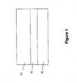
- FIG. 1is a schematic illustration of a basic capacitor structure.
- FIG. 2is a schematic side view of the structure of a DRAM capacitor after the formation of a conductor peg and the deposition of capacitor thin films.
- FIG. 3is a schematic side view of the structure of a DRAM capacitor after the formation of a capacitor hollow and the deposition of capacitor thin films.
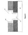
- FIG. 4is a schematic side view of the structure of a DRAM trench capacitor.
- FIG. 5is a schematic illustration of a semiconductor substrate comprising a high-k dielectric layer after deposition of a conductive noble metal oxide layer by ALD and prior to patterning to form a gate electrode.
- FIG. 6is a schematic illustration of a dual damascene structure comprising a noble metal barrier layer.
- FIG. 7is a schematic illustration of a dual damascene structure comprising a noble metal seed layer.
- FIG. 8illustrates the growth rate and sensitivity of IrO 2 film as a function of ozone pulse length.
- the solid squaresindicate IrO 2 growth rate on soda lime glass substrates.
- the deposition temperaturewas about 175° C.
- FIG. 9illustrates the growth rate and resistivity of ALD deposited IrO 2 films as a function of the ozone dose.
- the solid squaresindicate IrO 2 growth rate on soda lime glass substrates.
- the deposition temperaturewas about 175° C.
- FIG. 10shows the XRD pattern of IrO 2 thin film deposited by ALD on a silicon substrate at about 175° C.
- Noble metal oxide thin filmscan be deposited on a substrate by atomic layer deposition (ALD) type processes.
- ALD type processesare based on controlled, self-limiting surface reactions of precursor chemicals. Gas phase reactions are avoided by feeding the precursors alternately and sequentially into the reaction chamber. Vapor phase reactants are separated from each other in the reaction chamber, for example, by removing excess reactants and/or reactant by-products from the reaction chamber between reactant pulses.
- a substrateis loaded into a reaction chamber and is heated to a suitable deposition temperature, generally at lowered pressure.
- Deposition temperaturesare maintained below the precursor thermal decomposition temperature but at a high enough level to avoid condensation of reactants and to provide the activation energy for the desired surface reactions.
- the appropriate temperature window for any given ALD reactionwill depend upon the surface termination and reactant species involved.
- the temperatureis preferably at or below about 300° C., more preferably at or below about 200° C.
- a first reactantis conducted into the chamber in the form of vapor phase pulse and contacted with the surface of the substrate. Conditions are preferably selected such that no more than about one monolayer of the precursor is adsorbed on the substrate surface in a self-limiting manner. Excess first reactant and reaction byproducts, if any, are purged from the reaction chamber, often with a pulse of inert gas such as nitrogen or argon.
- Purging the reaction chambermeans that vapor phase precursors and/or vapor phase byproducts are removed from the reaction chamber such as by evacuating the chamber with a vacuum pump and/or by replacing the gas inside the reactor with an inert gas such as argon or nitrogen.
- Typical purging timesare from about 0.05 to 20 seconds, more preferably between about 1 and 10, and still more preferably between about 1 and 2 seconds.
- other purge timescan be utilized if necessary, such as when depositing noble metal oxides in situations where highly conformal step coverage over extremely high aspect ratio structures or other structures with complex surface morphology is needed, such as in Micro-Electro-Mechanical Systems (MEMS).
- MEMSMicro-Electro-Mechanical Systems
- the appropriate pulsing timescan be readily determined by the skilled artisan based on the particular circumstances.
- a second gaseous reactantis pulsed into the chamber where it reacts with the first reactant bound to the surface. Excess second reactant and gaseous by-products of the surface reaction are purged out of the reaction chamber, preferably with the aid of an inert gas. The steps of pulsing and purging are repeated until a thin film of the desired thickness has been formed on the substrate, with each cycle leaving no more than a molecular monolayer.
- each pulse or phase of each cycleis preferably self-limiting.
- An excess of reactant precursorsis supplied in each phase to saturate the susceptible structure surfaces.
- Surface saturationensures reactant occupation of all available reactive sites (subject, for example, to physical size or “steric hindrance” restraints) and thus ensures excellent step coverage.
- a noble metal oxide thin filmis formed on a substrate by an ALD type process comprising multiple pulsing cycles, each cycle comprising:
- the noble metal thin oxide filmtypically comprises multiple monolayers of a single noble metal oxide.
- the final metal structuremay comprise two or more different noble metal oxides.
- the growthcan be started with the deposition of a first noble metal oxide and ended with the deposition of a second noble metal oxide.
- alternating layers of noble metal oxidescan be deposited.
- the substratecan comprise various types of materials.
- the substratetypically comprises a number of thin films with varying chemical and physical properties.
- the substratemay comprise a dielectric layer, such as aluminum oxide, hafnium oxide, hafnium silicate, tantalum oxide, zirconium oxide, a metal, such as Ta, Ti, or W, a metal nitride, such as TaN, TiN, NbN, MoN or WN, silicon, silicon germanium, germanium or polysilicon.
- the substrate surfacemay have been patterned and may comprise structures such as nodes, vias, trenches or micromechanical systems (MEMS).
- MEMSmicromechanical systems
- the noble metal oxideis preferably selected from the group consisting of Ru, Re, Os and Ir oxides and is preferably electrically conductive.
- Suitable noble metal precursorsmay be selected by the skilled artisan. In general, metal compounds where the metal is bound or coordinated to oxygen, nitrogen, carbon or a combination thereof are preferred. In some embodiments the noble metal precursors are organic compounds. More preferably betadiketonate compounds are used. In some embodiments, X(acac) 3 or X(thd) y compounds are used, where X is a noble metal, y is generally, but not necessarily between 2 and 3 and thd is 2,2,6,6-tetramethyl-3,5-heptanedionato.
- preferred metal precursorscan be selected from the group consisting of ruthenium betadiketonate compounds, ruthenium cyclopentadienyl compounds, ruthenium carbonyl compounds and combinations thereof.
- the ruthenium precursormay also comprise one or more halide ligands.
- the precursoris Ru(acac) 3 or Ru(thd) 3 .
- electrically conductive Ru oxidepreferably RuO 2
- a Ru precursorpreferably comprises a betadiketonate and more preferably is Ru(acac) 3 .
- the temperatureis preferably less than about 300° C., more preferably less than about 200° C.
- preferred metal precursorsmay be selected from the group consisting of rhenium betadiketonate compounds, rhenium cyclopentadienyl compounds, rhenium carbonyl compounds and combinations thereof.
- the rhenium precursormay also comprise one or more halide ligands.
- the precursoris Re(acac) 3 or Re(thd) 3 .
- electrically conductive Re oxidepreferably ReO 2 , Re 2 O 5 , Re 2 O 7 or ReO 3
- the Re precursoris preferably comprises a betadiketonate compound and more preferably is Re(acac) 3 .
- the temperatureis preferably less than about 300° C., more preferably less than about 200° C.
- preferred metal precursorsmay be selected from the group consisting of osmium betadiketonate compounds, osmium cyclopentadienyl compounds, osmium carbonyl compounds and combinations thereof.
- the osmium precursormay also comprise one or more halide ligands.
- the precursoris Os(acac) 3 or Os(thd) 3 .
- electrically conductive Os oxidepreferably OsO 2
- Os precursoris preferably comprises a betadiketonate compound and more preferably is Os(acac) 3 .
- the temperatureis preferably less than about 300° C., more preferably less than about 200° C.
- preferred metal precursorsmay be selected from the group consisting of iridium betadiketonate compounds, iridium cyclopentadienyl compounds, iridium carbonyl compounds and combinations thereof.
- the iridium precursormay also comprise one or more halide ligands.
- the precursoris Ir(acac) 3 or Ir(thd) 3 .
- electrically conductive Ir oxidepreferably IrO 2
- Ir precursoris preferably comprises a betadiketonate compound and more preferably is Ir(acac) 3 .
- the temperatureis preferably less than about 300° C., more preferably less than about 200° C.
- the noble metal precursor employed in the ALD type processesmay be solid, liquid or gaseous material under standard conditions (room temperature and atmospheric pressure), provided that the metal precursor is in vapor phase before it is conducted into the reaction chamber and contacted with the substrate surface.
- “Pulsing” a vaporized precursor onto the substratemeans that the precursor vapor is conducted into the chamber for a limited period of time. Typically, the pulsing time is from about 0.05 to 10 seconds. However, depending on the substrate type and its surface area, the pulsing time may be even higher than 10 seconds.
- the noble metal precursoris pulsed for from 0.05 to 10 seconds, more preferably for from 0.1 to 5 seconds and most preferably for about 0.3 to 3.0 seconds.
- the oxygen-containing precursoris preferably pulsed for from about 0.05 to 10 seconds, more preferably for from 0.1 to 5 seconds, most preferably about for from 0.2 to 3.0 seconds.
- pulsing timescan be on the order of minutes in some cases. The optimum pulsing time can be readily determined by the skilled artisan based on the particular circumstances.
- the mass flow rate of the noble metal precursorcan be determined by the skilled artisan. In one embodiment, for deposition on 300 mm wafers the flow rate of noble metal precursor is preferably between about 1 and 1000 sccm without limitation, more preferably between about 100 and 500 sccm.
- the mass flow rate of the noble metal precursoris usually lower than the mass flow rate of the oxygen source, which is usually between about 10 and 10000 sccm without limitation, more preferably between about 100-2000 sccm and most preferably between 100-1000 sccm.
- the pressure in the reaction chamberis typically from about 0.01 and 20 mbar, more preferably from about 1 to about 10 mbar. However, in some cases the pressure will be higher or lower than this range, as can be readily determined by the skilled artisan.
- the oxygen sourcemay be an oxygen-containing gas pulse and can be a mixture of oxygen and inactive gas, such as nitrogen or argon.
- the oxygen sourcemay be a molecular oxygen-containing gas pulse.
- the preferred oxygen content of the oxygen-source gasis from about 10 to 25%.
- one source of oxygenmay be air.
- the oxygen sourcecomprises an activated or excited oxygen species.
- the oxygen sourcecomprises ozone.
- the oxygen sourcemay be pure ozone or a mixture of ozone and another gas, for example an inactive gas such as nitrogen or argon.
- the oxygen sourceis oxygen plasma.
- the noble metal ALD processtypically comprises alternating pulses of noble metal precursor and a reactant comprising an oxygen source.
- the oxygen source pulsemay be provided, for example, by pulsing ozone or a mixture of ozone and another gas into the reaction chamber.
- ozoneis formed inside the reactor, for example by conducting oxygen containing gas through an arc.
- an oxygen containing plasmais formed in the reactor.
- the plasmamay be formed in situ on top of the substrate or in close proximity to the substrate.
- the plasmais formed upstream of the reaction chamber in a remote plasma generator and plasma products are directed to the reaction chamber to contact the substrate.
- the pathway to the substratecan be optimized to maximize electrically neutral species and minimize ion survival before reaching the substrate.
- the pressure in the reaction spaceis typically between about 0.01 and 20 mbar, more preferably between about 1 and 10 mbar.
- the substrateBefore starting the deposition of the film, the substrate is typically heated to a suitable growth temperature.
- the growth temperature of the metal thin filmis less than about 300° C., more preferably less than about 250° C. and even more preferably less than about 200° C.
- the preferred deposition temperaturemay vary depending on a number of factors such as, and without limitation, the reactant precursors, the pressure, flow rate, the arrangement of the reactor, and the composition of the substrate including the nature of the material to be deposited on.
- the specific growth temperaturemay be selected by the skilled artisan using routine experimentation.
- the processing timedepends on the thickness of the layer to be produced and the growth rate of the film.
- the growth rate of a thin filmis determined as thickness increase per one cycle.
- One cycleconsists of the pulsing and purging steps of the precursors and the duration of one cycle is typically between about 0.2 and 30 seconds, more preferably between about 1 and 10 seconds, but it can be on order of minutes or more in some cases.
- ALD equipmentsuch as the F-120® reactor, Pulsar® reactor and EmerALDTM reactor, available from ASM America, Inc of Phoenix, Ariz.
- many other kinds of reactors capable of ALD growth of thin filmsincluding CVD reactors equipped with appropriate equipment and means for pulsing the precursors, can be employed.
- reactantsare kept separate until reaching the reaction chamber, such that shared lines for the precursors are minimized.
- other arrangementsare possible, such as the use of a pre-reaction chamber as described in U.S. application Ser. Nos. 10/929,348, filed Aug. 30, 2004 and 09/836,674, filed Apr. 16, 2001, the disclosures of which are incorporated herein by reference.
- the growth processescan optionally be carried out in a reactor or reaction space connected to a cluster tool.
- a cluster toolbecause each reaction space is dedicated to one type of process, the temperature of the reaction space in each module can be kept constant, which improves the throughput compared to a reactor in which is the substrate is heated up to the process temperature before each run.
- a stand-alone reactorcan be equipped with a load-lock. In that case, it is not necessary to cool down the reaction space between each run.
- capacitor electrodesWhile illustrated in the context of formation of capacitor electrodes, gate electrodes, barrier and seed layers, the skilled artisan will readily find application for the principles and advantages disclosed herein in other contexts.
- the ALD processmay be used to deposit electrically conductive noble metal oxide thin films which form capacitor electrodes.
- a basic capacitor structureis illustrated in FIG. 1 , in which a storage electrode 10 is separated from a reference electrode 20 by a high k layer 15 .
- One or both of the storage electrode 10 and reference electrode 20may be formed by an ALD deposited conductive noble metal oxide thin film.
- the ALD process for depositing noble metal oxide filmscan be used to form one or both electrodes in capacitors of any form, including, without limitation, a stud capacitor, a trench capacitor, and a container capacitor. Several particular embodiments are described below.
- the nature of the ALD processallows for conformal deposition on structures with complex morphology, such as three-dimensional folding structures and HSG silicon that are commonly used in forming capacitors, particularly for dense memory array structures, such as dynamic random access memories (DRAMs).
- DRAMsdynamic random access memories
- a silicon substrate 30is provided, with a doped region 34 that is an active part of a transistor, as illustrated in FIG. 2 .
- Field oxide 32separates the transistors from each other.
- An insulator layer 36e,g., SiO 2 , is grown on the substrate and a via is etched through the insulator and filled with a conductor material 50 , e.g. polysilicon.
- the polysilicon layeris patterned and etched so that the via plug and a tooth-like extension over the plug remain on the structure.
- a noble metal oxidecould be used in place of the polysilicon, the polysilicon tooth minimizes the amount of expensive metal that is needed for the lower electrode.
- a barrier layer 52e.g., tantalum silicon nitride Ta x Si y N z , may be deposited over the substrate by, e.g., Atomic Layer Deposition (ALD).
- a barrier layeris patterned and etched so that there is barrier layer left only on and near the polysilicon surface.
- the barrier layermay be omitted, for example if a noble metal oxide with good barrier properties is utilized as the lower electrode.
- a conductive noble metal oxide lower electrode 54is grown by ALD on the substrate as described above and then the noble metal oxide layer is patterned and etched so that there is metal oxide left only on and near the barrier layer 52 .
- a capacitor insulator 56is deposited on the substrate.
- the capacitor insulator 56preferably has a high dielectric constant, i.e., it is a high-k material.
- the high-k materialpreferably has a dielectric constant greater than about 5. In some embodiments the dielectric constant is greater than about 10 and in other embodiments it is greater than about 20.
- the high-k layeris optionally annealed to increase the crystallinity and dielectric constant of the layer.
- an upper electrode 58comprising a noble metal oxide is deposited on the high-k material 56 , and patterned and etched so that the capacitor can be addressed (electrically accessed).
- all memory cells for one arrayare accessed by a common reference electrode, such that patterning within the array may involve only creating openings for cell contacts, such as bit line plugs.
- only one of the lower 54 or upper electrode 58comprises a noble metal oxide deposited by ALD. In this case, the other electrode can be formed by conventional means.
- Another way of constructing the capacitoris to planarize the substrate surface after the deposition of polysilicon and then form a metal knob of polysilicon.
- a relatively thick layer of metalis needed on the polysilicon plug to increase the effective area of the capacitor.
- the noble metal oxide deposited by ALDforms the part of the “tooth” that extends above the insulator 36 plane.
- the effective area of the capacitorcan also be increased by etching a hollow on a surface and form a capacitor structure on the walls and the bottom of the hollow.
- a polysilicon plug 50extending through the first insulator layer 36 .
- a second insulator layer 70e.g., SiO 2
- the second insulator 70is etched until a capacitor hollow 96 is formed.
- a barrier layer 76e.g., Ta x Si y N z , may deposited on the substrate and patterned so that only the top surface of the polysilicon plug is covered with the barrier 76 .
- the barrier layermay be omitted, for example if a noble metal oxide with good barrier properties is utilized as the lower electrode.
- a lower metal electrode 90 comprising a conductive noble metal oxideis deposited by ALD on the substrate as described above and patterned and etched so that only the bottom and the walls of the hollow are covered with the lower metal electrode 90 .
- the second insulation layer 70can be removed at this stage to expose the outside surfaces of the cup-like shape.
- High-k dielectric layer 92e.g. BST, is grown on the substrate by e.g. ALD.
- An optional annealing stepmay be used to increase the crystallinity and dielectric constant of the dielectric layer 92 .
- the upper metal electrode 94is formed by depositing a conductive noble metal oxide by ALD on the high-k thin film 92 according to the methods discussed above. In some embodiments only one of the upper electrode 94 and lower electrode 90 is formed by depositing a noble metal oxide by ALD and the other electrode is formed conventionally.
- FIG. 4shows a trench capacitor without the addressing lines and semiconducting active components.
- a silicon substrate 110there is a trench with a surface that has been covered with a multi-layer thin film 112 .
- the depositionhas started with the formation of a barrier layer 114 , e.g., Ta x Si y N z , which is preferably formed between the silicon and a conductive noble metal oxide.
- the barrier layer 114may be omitted.
- a first electrode 116 comprising a noble metal oxideis deposited by ALD as described above.
- a high-k layer 118e.g., BST, is grown e.g., by ALD.
- a second electrode layer 120 comprising a noble metal oxideis grown by ALD as described above.
- a barrier thin film 122e.g., Ta x Si y N z , although in some embodiments, such as where the second electrode layer has good barrier properties, the barrier thin film 122 may be omitted.
- one of the first and second electrodescomprises a noble metal oxide film deposited by ALD and the other is formed conventionally.
- the silicon substratecomprises the lower electrode.
- the thickness of the metal oxide electrodesis typically selected from approximately 1 ⁇ m up to about 200 nm and even more depending on the application.
- the conductive noble metal oxides used as capacitor electrodes in these embodimentsis preferably selected from the group consisting of Ru, Re, Os and Ir oxides.
- a gate electrodeis formed by ALD of a conductive noble metal oxide.
- a silicon substrate 150is illustrated comprising a layer of high-k dielectric material 160 .
- the substratemay be treated prior to deposition of the high-k material 160 .
- a thin interfacial layer(not shown) may be formed prior to deposition of the high-k material 160 .
- a thin chemical oxide or oxynitrideis formed on the surface.
- a thermal oxideis grown on the substrate.
- High-kgenerally refers to a dielectric material having a dielectric constant (k) value greater than that of silicon oxide.
- the high-k materialhas a dielectric constant greater than 5, more preferably greater than about 10.
- Exemplary high-k materialsinclude, without limitation, HfO 2 , ZrO 2 , Al 2 O 3 , TiO 2 , Ta 2 O 5 , Sc 2 O 3 , lanthanide oxides and mixtures thereof, silicates and materials such as YSZ (yttria-stabilized zirconia), barium strontium titanate (BST), strontium titanate (ST), strontium bismuth tantalate (SBT) and bismuth tantalate (BT).
- the high-k materialis also deposited by an ALD process.
- a layer of conductive noble metal oxide 180is deposited over the high-k material 160 by ALD, as described above, to form the structure illustrated in FIG. 5 .
- the noble metal oxide 180 and underlying high-k material 160are patterned to form a gate electrode.
- the noble metal oxide thin film 180is preferably deposited over the dielectric layer 160 by contacting the substrate with alternating pulses of a noble metal source chemical and an oxygen source chemical as described above.
- the noble metal source chemicalis preferably a betadiketonate compound and the oxygen source chemical is preferably ozone or oxygen plasma products. Unreacted source chemicals and reaction byproducts are removed from the reaction chamber after each source chemical pulse, for example by evacuation and/or purging with an inert gas.
- the pulsing cycleis repeated until a noble metal oxide layer of the desired thickness has been formed.
- the noble metal oxide layerhas a thickness between about 3 nm and about 50 nm.
- the conductive noble metal oxides deposited to form the gate electrode in these embodimentsare preferably selected from the group consisting of Ru, Re, Os and Ir oxides.
- the noble metal oxide 180forms the gate electrode.
- another conductive materialsuch as a metal or poly-Si, is deposited over the noble metal oxide 180 .
- the additional conductive materialmay be deposited by ALD or by another deposition process, such as by CVD or PVD. The deposition may be selective, or may be followed by patterning steps.
- a noble metal oxide thin filmcan also be deposited by ALD to form a barrier layer for interconnect metallization.
- the substratemay comprise damascene or dual damascene structures, including high aspect ratio trenches and vias.
- a substrate 200comprising a trench 210 and via 220 , as illustrated in FIG. 6 , is placed in an ALD reaction chamber.
- a noble metal oxide thin film barrier layer 250is then deposited over the trench 210 and via 220 by contacting the substrate 200 with alternating pulses of a noble metal source chemical and an oxygen source.
- the noble metal source chemicalis preferably a betadiketonate compound.
- the oxygen sourceis preferably ozone or oxygen plasma products.
- Unreacted source chemicals and reaction byproductsare removed from the reaction chamber after each source chemical pulse by purging.
- the pulsing cycleis repeated until a barrier layer 250 of the desired thickness has been formed.
- the barrier layerhas a thickness between about 1 nm and about 10 nm.
- a noble metal oxide filmis deposited by ALD to form a seed layer for interconnect metallization.
- the seed layermay be deposited, for example, over a damascene or dual damascene structure.
- a substrate 300comprising a trench 310 and via 320 is placed in the reaction chamber of an ALD reactor ( FIG. 7 ).
- the structurepreferably comprises a diffusion barrier layer 330 , which may have been deposited by ALD, for example as described above.
- the substrate 300is heated to the deposition temperature, preferably less than about 300° C., more preferably less than about 250° C., and still more preferably less than about 200° C.
- the substrate 300is contacted with alternating and sequential pulses of a noble metal precursor and an oxygen source.
- Pulses of reactantsare separated by purging the chamber, preferably by a combination of evacuation with a vacuum pump while flowing an inert gas, such as argon or nitrogen.
- the pulsing cycleis repeated until a noble metal oxide seed layer 350 of the desired thickness has been formed.
- the thickness of the seed layeris between about 1 nm and about 30 nm or more, depending on the dimensions of the vias and trenches.
- the noble metal oxide layeris used as a seed layer for metallization, for example copper deposition by electroplating or a CVD process.
- IrO 2was deposited by ALD on 5 ⁇ 5 cm 2 soda glass and Si(111) substrates. The substrates were contacted with alternating pulses of Ir(acac) 3 and ozone at a temperature of about 175° C.
- RhO 2 filmswere grown on 5 ⁇ 5 cm soda glass and Si(111) substrates by contacting them with alternating pulses of Rh(acac) 3 and ozone at a temperature of about 175° C. to about 200° C.
- the filmswere grayish and semitransparent in color and partly reflective.
Landscapes
- Chemical & Material Sciences (AREA)
- General Chemical & Material Sciences (AREA)
- Chemical Kinetics & Catalysis (AREA)
- Engineering & Computer Science (AREA)
- Materials Engineering (AREA)
- Mechanical Engineering (AREA)
- Metallurgy (AREA)
- Organic Chemistry (AREA)
- Inorganic Chemistry (AREA)
- Semiconductor Memories (AREA)
- Chemical Vapour Deposition (AREA)
Abstract
Description
- 1. Field of the Invention
- The present invention relates generally to processes for producing noble metal oxide thin films on a substrate by atomic layer deposition.
- 2. Description of the Related Art
- Noble metal oxide thin films have high work function, good oxidation resistance and good barrier properties. As a result, they have a variety of potential applications in microelectronics and in other fields. For example, in the semiconductor industry noble metal oxides can be used as a material for electrodes in DRAMs and FRAMs, as gate electrodes in integrated circuits and as barrier and seed layers for interconnect metallization.
- ALD is a self-limiting process, whereby alternated pulses of reaction precursors saturate a substrate surface and leave no more than one monolayer of material per pulse. The deposition conditions and precursors are selected to ensure self-saturating reactions, such that an adsorbed layer in one pulse leaves a surface termination that is non-reactive with the gas phase reactants of the same pulse. A subsequent pulse of different reactants reacts with the previous termination to enable continued deposition. Thus, each cycle of alternated pulses leaves no more than about one molecular layer of the desired material. The principles of ALD type processes have been presented by T. Suntola, e.g. in the Handbook of Crystal Growth 3, Thin Films and Epitaxy, Part B: Growth Mechanisms and Dynamics, Chapter 14, Atomic Layer Epitaxy, pp. 601-663, Elsevier Science B.V. 1994, the disclosure of which is incorporated herein by reference. Variations of ALD have been proposed that allow for modulation of the growth rate. However, to provide for high conformality and thickness uniformity, these reactions are still more or less self-saturating.
- In a typical ALD process for depositing metal oxides, one deposition cycle comprises exposing the substrate to a metal precursor, removing unreacted first reactant and reaction byproducts from the reaction chamber, exposing the substrate to an oxygen precursor followed by a second removal step.
- Thin films of conductive noble metal oxides, particularly Ru, Re, Os and Ir oxides, can be deposited using atomic layer deposition. A substrate is alternately contacted with a noble metal precursor and a second reactant comprising an oxygen source. In preferred embodiments the noble metal precursor is a betadiketonate compound and the oxygen source is ozone or oxygen plasma. The atomic layer deposition reaction is preferably carried out at a temperature of about 300° C. or less, more preferably at a temperature of about 200° C. or less.
- In some embodiment, an atomic layer deposition process for forming a noble metal oxide thin film comprises alternately and sequentially contacting a substrate with a noble metal precursor and ozone or oxygen plasma. The noble metal precursor preferably comprises a noble metal selected from the group consisting of Ru, Re, Os and Ir. The precursor preferably comprises a noble metal may be bound to oxygen, nitrogen or carbon and more preferably is a betadiketonate compound such as X(acac)3, where X is Ru, Re, Os or Ir and acac is acetylacetone.
- The process is preferably carried out at a deposition temperature of less than about 300° C., more preferably less than about 200° C.
- In other embodiments, an electrically, conductive noble metal oxide is produced on a substrate by exposing the substrate in a reaction chamber to a vapor phase noble metal precursor such that no more than one monolayer of the precursor is adsorbed on the substrate. The excess noble metal precursor is removed and the substrate is subsequently exposed to ozone or oxygen plasma. Excess ozone is removed from the chamber and the cycle is repeated to form a film of the desired thickness. The noble metal precursor preferably comprises a noble metal selected from the group consisting of Ru, Re, Os and Ir and in some embodiments is preferably a betadiketonate compound. The process may be carried out at a temperature of less than about 300° C., more preferably less than about 200° C.
- In still other embodiments, an atomic layer deposition process is provided for forming a conductive noble metal oxide thin film on a substrate from vapor phase pulse of a noble metal source and an oxygen source, wherein the noble metal precursor comprises a noble metal selected from the group consisting of Ru, Re, Os and Ir and the process is carried out at a temperature of less than about 300° C., more preferably less than about 200° C.
- In further embodiments, an ALD type process is provided for depositing noble metal oxides comprising Re, Os and/or Ir. A substrate is alternately and sequentially contacted with a vapor phase betadiketonate noble metal source chemical and an oxygen source, such as ozone or oxygen plasma. The process may be carried out at a temperature of less than about 300° C., more preferably less than about 200° C.
- In some embodiments a capacitor electrode is formed by depositing an electrically conductive noble metal oxide by ALD.
- In other embodiments a gate electrode is formed by depositing a gate dielectric layer and depositing a noble metal oxide over the gate dielectric layer by an atomic layer deposition process.
- In still other embodiments, a barrier layer and/or seed layer in a metal interconnect structure is formed by depositing a noble metal oxide layer by ALD.
FIG. 1 is a schematic illustration of a basic capacitor structure.FIG. 2 is a schematic side view of the structure of a DRAM capacitor after the formation of a conductor peg and the deposition of capacitor thin films.FIG. 3 is a schematic side view of the structure of a DRAM capacitor after the formation of a capacitor hollow and the deposition of capacitor thin films.FIG. 4 is a schematic side view of the structure of a DRAM trench capacitor.FIG. 5 is a schematic illustration of a semiconductor substrate comprising a high-k dielectric layer after deposition of a conductive noble metal oxide layer by ALD and prior to patterning to form a gate electrode.FIG. 6 is a schematic illustration of a dual damascene structure comprising a noble metal barrier layer.FIG. 7 is a schematic illustration of a dual damascene structure comprising a noble metal seed layer.FIG. 8 illustrates the growth rate and sensitivity of IrO2film as a function of ozone pulse length. The solid squares indicate IrO2growth rate on soda lime glass substrates. The deposition temperature was about 175° C.FIG. 9 illustrates the growth rate and resistivity of ALD deposited IrO2films as a function of the ozone dose. The solid squares indicate IrO2growth rate on soda lime glass substrates. The deposition temperature was about 175° C.FIG. 10 shows the XRD pattern of IrO2thin film deposited by ALD on a silicon substrate at about 175° C.- Noble metal oxide thin films can be deposited on a substrate by atomic layer deposition (ALD) type processes. ALD type processes are based on controlled, self-limiting surface reactions of precursor chemicals. Gas phase reactions are avoided by feeding the precursors alternately and sequentially into the reaction chamber. Vapor phase reactants are separated from each other in the reaction chamber, for example, by removing excess reactants and/or reactant by-products from the reaction chamber between reactant pulses.
- Briefly, a substrate is loaded into a reaction chamber and is heated to a suitable deposition temperature, generally at lowered pressure. Deposition temperatures are maintained below the precursor thermal decomposition temperature but at a high enough level to avoid condensation of reactants and to provide the activation energy for the desired surface reactions. Of course, the appropriate temperature window for any given ALD reaction will depend upon the surface termination and reactant species involved. Here, the temperature is preferably at or below about 300° C., more preferably at or below about 200° C.
- A first reactant is conducted into the chamber in the form of vapor phase pulse and contacted with the surface of the substrate. Conditions are preferably selected such that no more than about one monolayer of the precursor is adsorbed on the substrate surface in a self-limiting manner. Excess first reactant and reaction byproducts, if any, are purged from the reaction chamber, often with a pulse of inert gas such as nitrogen or argon.
- Purging the reaction chamber means that vapor phase precursors and/or vapor phase byproducts are removed from the reaction chamber such as by evacuating the chamber with a vacuum pump and/or by replacing the gas inside the reactor with an inert gas such as argon or nitrogen. Typical purging times are from about 0.05 to 20 seconds, more preferably between about 1 and 10, and still more preferably between about 1 and 2 seconds. However, other purge times can be utilized if necessary, such as when depositing noble metal oxides in situations where highly conformal step coverage over extremely high aspect ratio structures or other structures with complex surface morphology is needed, such as in Micro-Electro-Mechanical Systems (MEMS). The appropriate pulsing times can be readily determined by the skilled artisan based on the particular circumstances.
- A second gaseous reactant is pulsed into the chamber where it reacts with the first reactant bound to the surface. Excess second reactant and gaseous by-products of the surface reaction are purged out of the reaction chamber, preferably with the aid of an inert gas. The steps of pulsing and purging are repeated until a thin film of the desired thickness has been formed on the substrate, with each cycle leaving no more than a molecular monolayer.
- As mentioned above, each pulse or phase of each cycle is preferably self-limiting. An excess of reactant precursors is supplied in each phase to saturate the susceptible structure surfaces. Surface saturation ensures reactant occupation of all available reactive sites (subject, for example, to physical size or “steric hindrance” restraints) and thus ensures excellent step coverage.
- According to a preferred embodiment, a noble metal oxide thin film is formed on a substrate by an ALD type process comprising multiple pulsing cycles, each cycle comprising:
- pulsing a vaporized noble metal precursor into the reaction chamber to form at most a molecular monolayer of the metal precursor on the substrate,
- purging the reaction chamber to remove excess noble metal precursor and reaction by products, if any,
- providing a pulse of a second reactant comprising an oxygen source, preferably ozone, onto the substrate,
- purging the reaction chamber to remove excess second reactant and any gaseous by-products formed in the reaction between the noble metal precursor layer on the first surface of the substrate and the second reactant, and
- repeating the pulsing and purging steps until a noble metal oxide thin film of the desired thickness has been formed.
- The noble metal thin oxide film typically comprises multiple monolayers of a single noble metal oxide. However, in other embodiments, the final metal structure may comprise two or more different noble metal oxides. For example, the growth can be started with the deposition of a first noble metal oxide and ended with the deposition of a second noble metal oxide. In other embodiments, alternating layers of noble metal oxides can be deposited.
- The substrate can comprise various types of materials. When manufacturing integrated circuits, the substrate typically comprises a number of thin films with varying chemical and physical properties. For example and without limitation, the substrate may comprise a dielectric layer, such as aluminum oxide, hafnium oxide, hafnium silicate, tantalum oxide, zirconium oxide, a metal, such as Ta, Ti, or W, a metal nitride, such as TaN, TiN, NbN, MoN or WN, silicon, silicon germanium, germanium or polysilicon. Further, the substrate surface may have been patterned and may comprise structures such as nodes, vias, trenches or micromechanical systems (MEMS).
- The noble metal oxide is preferably selected from the group consisting of Ru, Re, Os and Ir oxides and is preferably electrically conductive.
- Suitable noble metal precursors may be selected by the skilled artisan. In general, metal compounds where the metal is bound or coordinated to oxygen, nitrogen, carbon or a combination thereof are preferred. In some embodiments the noble metal precursors are organic compounds. More preferably betadiketonate compounds are used. In some embodiments, X(acac)3or X(thd)ycompounds are used, where X is a noble metal, y is generally, but not necessarily between 2 and 3 and thd is 2,2,6,6-tetramethyl-3,5-heptanedionato.
- When depositing ruthenium oxide thin films, preferred metal precursors can be selected from the group consisting of ruthenium betadiketonate compounds, ruthenium cyclopentadienyl compounds, ruthenium carbonyl compounds and combinations thereof. The ruthenium precursor may also comprise one or more halide ligands. In preferred embodiments, the precursor is Ru(acac)3or Ru(thd)3.
- In some embodiments electrically conductive Ru oxide, preferably RuO2, is deposited from alternating and sequential pulses of a Ru precursor and an oxygen source, preferably ozone. The Ru precursor preferably comprises a betadiketonate and more preferably is Ru(acac)3. The temperature is preferably less than about 300° C., more preferably less than about 200° C.
- When depositing rhenium oxide thin films, preferred metal precursors may be selected from the group consisting of rhenium betadiketonate compounds, rhenium cyclopentadienyl compounds, rhenium carbonyl compounds and combinations thereof. The rhenium precursor may also comprise one or more halide ligands. In preferred embodiments, the precursor is Re(acac)3or Re(thd)3.
- In some embodiments electrically conductive Re oxide, preferably ReO2, Re2O5, Re2O7or ReO3, is deposited from alternating and sequential pulses of a Re precursor and an oxygen source, preferably ozone. The Re precursor is preferably comprises a betadiketonate compound and more preferably is Re(acac)3. The temperature is preferably less than about 300° C., more preferably less than about 200° C.
- When depositing osmium oxide thin films, preferred metal precursors may be selected from the group consisting of osmium betadiketonate compounds, osmium cyclopentadienyl compounds, osmium carbonyl compounds and combinations thereof. The osmium precursor may also comprise one or more halide ligands. In preferred embodiments, the precursor is Os(acac)3or Os(thd)3.
- In some embodiments electrically conductive Os oxide, preferably OsO2, is deposited from alternating and sequential pulses of an Os precursor and an oxygen source, preferably ozone. The Os precursor is preferably comprises a betadiketonate compound and more preferably is Os(acac)3. The temperature is preferably less than about 300° C., more preferably less than about 200° C.
- When depositing iridium oxide thin films, preferred metal precursors may be selected from the group consisting of iridium betadiketonate compounds, iridium cyclopentadienyl compounds, iridium carbonyl compounds and combinations thereof. The iridium precursor may also comprise one or more halide ligands. In preferred embodiments, the precursor is Ir(acac)3or Ir(thd)3.
- In some embodiments electrically conductive Ir oxide, preferably IrO2, is deposited from alternating and sequential pulses of an Ir precursor and an oxygen source, preferably ozone. The Ir precursor is preferably comprises a betadiketonate compound and more preferably is Ir(acac)3. The temperature is preferably less than about 300° C., more preferably less than about 200° C.
- The noble metal precursor employed in the ALD type processes may be solid, liquid or gaseous material under standard conditions (room temperature and atmospheric pressure), provided that the metal precursor is in vapor phase before it is conducted into the reaction chamber and contacted with the substrate surface. “Pulsing” a vaporized precursor onto the substrate means that the precursor vapor is conducted into the chamber for a limited period of time. Typically, the pulsing time is from about 0.05 to 10 seconds. However, depending on the substrate type and its surface area, the pulsing time may be even higher than 10 seconds.
- Preferably, for a 300 mm wafer in a single wafer ALD reactor, the noble metal precursor is pulsed for from 0.05 to 10 seconds, more preferably for from 0.1 to 5 seconds and most preferably for about 0.3 to 3.0 seconds. The oxygen-containing precursor is preferably pulsed for from about 0.05 to 10 seconds, more preferably for from 0.1 to 5 seconds, most preferably about for from 0.2 to 3.0 seconds. However, pulsing times can be on the order of minutes in some cases. The optimum pulsing time can be readily determined by the skilled artisan based on the particular circumstances.
- The mass flow rate of the noble metal precursor can be determined by the skilled artisan. In one embodiment, for deposition on 300 mm wafers the flow rate of noble metal precursor is preferably between about 1 and 1000 sccm without limitation, more preferably between about 100 and 500 sccm. The mass flow rate of the noble metal precursor is usually lower than the mass flow rate of the oxygen source, which is usually between about 10 and 10000 sccm without limitation, more preferably between about 100-2000 sccm and most preferably between 100-1000 sccm.
- The pressure in the reaction chamber is typically from about 0.01 and 20 mbar, more preferably from about 1 to about 10 mbar. However, in some cases the pressure will be higher or lower than this range, as can be readily determined by the skilled artisan.
- The oxygen source may be an oxygen-containing gas pulse and can be a mixture of oxygen and inactive gas, such as nitrogen or argon. In some embodiments the oxygen source may be a molecular oxygen-containing gas pulse. The preferred oxygen content of the oxygen-source gas is from about 10 to 25%. Thus, one source of oxygen may be air. In preferred embodiments the oxygen source comprises an activated or excited oxygen species. In some embodiments the oxygen source comprises ozone. The oxygen source may be pure ozone or a mixture of ozone and another gas, for example an inactive gas such as nitrogen or argon. In other embodiments the oxygen source is oxygen plasma.
- As mentioned above, the noble metal ALD process typically comprises alternating pulses of noble metal precursor and a reactant comprising an oxygen source. The oxygen source pulse may be provided, for example, by pulsing ozone or a mixture of ozone and another gas into the reaction chamber. In other embodiments, ozone is formed inside the reactor, for example by conducting oxygen containing gas through an arc. In other embodiments an oxygen containing plasma is formed in the reactor. In some embodiments the plasma may be formed in situ on top of the substrate or in close proximity to the substrate. In other embodiments the plasma is formed upstream of the reaction chamber in a remote plasma generator and plasma products are directed to the reaction chamber to contact the substrate. As will be appreciated by the skilled artisan, in the case of a remote plasma the pathway to the substrate can be optimized to maximize electrically neutral species and minimize ion survival before reaching the substrate.
- The pressure in the reaction space is typically between about 0.01 and 20 mbar, more preferably between about 1 and 10 mbar.
- Before starting the deposition of the film, the substrate is typically heated to a suitable growth temperature. Preferably, the growth temperature of the metal thin film is less than about 300° C., more preferably less than about 250° C. and even more preferably less than about 200° C. The preferred deposition temperature may vary depending on a number of factors such as, and without limitation, the reactant precursors, the pressure, flow rate, the arrangement of the reactor, and the composition of the substrate including the nature of the material to be deposited on. The specific growth temperature may be selected by the skilled artisan using routine experimentation.
- The processing time depends on the thickness of the layer to be produced and the growth rate of the film. In ALD, the growth rate of a thin film is determined as thickness increase per one cycle. One cycle consists of the pulsing and purging steps of the precursors and the duration of one cycle is typically between about 0.2 and 30 seconds, more preferably between about 1 and 10 seconds, but it can be on order of minutes or more in some cases.
- Examples of suitable reactors that may be used for the deposition of thin films according to the processes of the present invention include commercially available ALD equipment such as the F-120® reactor, Pulsar® reactor and EmerALD™ reactor, available from ASM America, Inc of Phoenix, Ariz. In addition to these ALD reactors, many other kinds of reactors capable of ALD growth of thin films, including CVD reactors equipped with appropriate equipment and means for pulsing the precursors, can be employed. Preferably, reactants are kept separate until reaching the reaction chamber, such that shared lines for the precursors are minimized. However, other arrangements are possible, such as the use of a pre-reaction chamber as described in U.S. application Ser. Nos. 10/929,348, filed Aug. 30, 2004 and 09/836,674, filed Apr. 16, 2001, the disclosures of which are incorporated herein by reference.
- The growth processes can optionally be carried out in a reactor or reaction space connected to a cluster tool. In a cluster tool, because each reaction space is dedicated to one type of process, the temperature of the reaction space in each module can be kept constant, which improves the throughput compared to a reactor in which is the substrate is heated up to the process temperature before each run.
- A stand-alone reactor can be equipped with a load-lock. In that case, it is not necessary to cool down the reaction space between each run.
- While illustrated in the context of formation of capacitor electrodes, gate electrodes, barrier and seed layers, the skilled artisan will readily find application for the principles and advantages disclosed herein in other contexts.
- Formation of Capacitor Electrodes
- The ALD process may be used to deposit electrically conductive noble metal oxide thin films which form capacitor electrodes. A basic capacitor structure is illustrated in
FIG. 1 , in which astorage electrode 10 is separated from areference electrode 20 by ahigh k layer 15. One or both of thestorage electrode 10 andreference electrode 20 may be formed by an ALD deposited conductive noble metal oxide thin film. One of skill in the art will recognize that the ALD process for depositing noble metal oxide films can be used to form one or both electrodes in capacitors of any form, including, without limitation, a stud capacitor, a trench capacitor, and a container capacitor. Several particular embodiments are described below. The nature of the ALD process allows for conformal deposition on structures with complex morphology, such as three-dimensional folding structures and HSG silicon that are commonly used in forming capacitors, particularly for dense memory array structures, such as dynamic random access memories (DRAMs). - In one embodiment, a
silicon substrate 30 is provided, with a dopedregion 34 that is an active part of a transistor, as illustrated inFIG. 2 .Field oxide 32 separates the transistors from each other. Aninsulator layer 36, e,g., SiO2, is grown on the substrate and a via is etched through the insulator and filled with aconductor material 50, e.g. polysilicon. The polysilicon layer is patterned and etched so that the via plug and a tooth-like extension over the plug remain on the structure. Although a noble metal oxide could be used in place of the polysilicon, the polysilicon tooth minimizes the amount of expensive metal that is needed for the lower electrode. The exposed surface of the polysilicon may be very rough after the etching step so that the surface area of polysilicon is as large as possible. Abarrier layer 52, e.g., tantalum silicon nitride TaxSiyNz, may be deposited over the substrate by, e.g., Atomic Layer Deposition (ALD). The barrier layer is patterned and etched so that there is barrier layer left only on and near the polysilicon surface. In some embodiments the barrier layer may be omitted, for example if a noble metal oxide with good barrier properties is utilized as the lower electrode. - A conductive noble metal oxide
lower electrode 54 is grown by ALD on the substrate as described above and then the noble metal oxide layer is patterned and etched so that there is metal oxide left only on and near thebarrier layer 52. After that acapacitor insulator 56 is deposited on the substrate. Thecapacitor insulator 56 preferably has a high dielectric constant, i.e., it is a high-k material. The high-k material preferably has a dielectric constant greater than about 5. In some embodiments the dielectric constant is greater than about 10 and in other embodiments it is greater than about 20. The high-k layer is optionally annealed to increase the crystallinity and dielectric constant of the layer. Finally, anupper electrode 58 comprising a noble metal oxide is deposited on the high-k material 56, and patterned and etched so that the capacitor can be addressed (electrically accessed). In some arrangements all memory cells for one array are accessed by a common reference electrode, such that patterning within the array may involve only creating openings for cell contacts, such as bit line plugs. In some embodiments only one of the lower54 orupper electrode 58 comprises a noble metal oxide deposited by ALD. In this case, the other electrode can be formed by conventional means. - Another way of constructing the capacitor is to planarize the substrate surface after the deposition of polysilicon and then form a metal knob of polysilicon. However, a relatively thick layer of metal is needed on the polysilicon plug to increase the effective area of the capacitor. In that case the noble metal oxide deposited by ALD forms the part of the “tooth” that extends above the
insulator 36 plane. - The effective area of the capacitor can also be increased by etching a hollow on a surface and form a capacitor structure on the walls and the bottom of the hollow. As shown in
FIG. 3 , there is apolysilicon plug 50 extending through thefirst insulator layer 36. A second insulator layer70 (e.g., SiO2) is deposited on the first insulator layer and patterned. Thesecond insulator 70 is etched until a capacitor hollow96 is formed. Abarrier layer 76, e.g., TaxSiyNz, may deposited on the substrate and patterned so that only the top surface of the polysilicon plug is covered with thebarrier 76. However, in some embodiments the barrier layer may be omitted, for example if a noble metal oxide with good barrier properties is utilized as the lower electrode. - A
lower metal electrode 90 comprising a conductive noble metal oxide is deposited by ALD on the substrate as described above and patterned and etched so that only the bottom and the walls of the hollow are covered with thelower metal electrode 90. Optionally thesecond insulation layer 70 can be removed at this stage to expose the outside surfaces of the cup-like shape. High-k dielectric layer 92, e.g. BST, is grown on the substrate by e.g. ALD. An optional annealing step may be used to increase the crystallinity and dielectric constant of thedielectric layer 92. Finally, theupper metal electrode 94, is formed by depositing a conductive noble metal oxide by ALD on the high-kthin film 92 according to the methods discussed above. In some embodiments only one of theupper electrode 94 andlower electrode 90 is formed by depositing a noble metal oxide by ALD and the other electrode is formed conventionally. - Still another way of increasing the effective area of the DRAM capacitor while keeping the reserved substrate area to a minimum is to place the capacitor structure in a deep pit etched on silicon substrate. The structure is typically referred to as a trench capacitor.
FIG. 4 shows a trench capacitor without the addressing lines and semiconducting active components. In asilicon substrate 110 there is a trench with a surface that has been covered with a multi-layerthin film 112. The deposition has started with the formation of abarrier layer 114, e.g., TaxSiyNz, which is preferably formed between the silicon and a conductive noble metal oxide. However, in some embodiments, for example if the conductive noble metal oxide has good barrier properties, thebarrier layer 114 may be omitted. - On the barrier layer114 a
first electrode 116 comprising a noble metal oxide is deposited by ALD as described above. On the first electrode layer116 a high-k layer 118, e.g., BST, is grown e.g., by ALD. On the high-k layer118 asecond electrode layer 120 comprising a noble metal oxide is grown by ALD as described above. In the case where the trench will be filled withpolysilicon 124, it is preferable to protect thesecond electrode 120 with a barrierthin film 122, e.g., TaxSiyNz, although in some embodiments, such as where the second electrode layer has good barrier properties, the barrierthin film 122 may be omitted. - In some embodiments, one of the first and second electrodes comprises a noble metal oxide film deposited by ALD and the other is formed conventionally. In other embodiments, the silicon substrate comprises the lower electrode.
- In each embodiment, the thickness of the metal oxide electrodes is typically selected from approximately 1 μm up to about 200 nm and even more depending on the application.
- The conductive noble metal oxides used as capacitor electrodes in these embodiments is preferably selected from the group consisting of Ru, Re, Os and Ir oxides.
- Formation of a Gate Electrode
- In some embodiments a gate electrode is formed by ALD of a conductive noble metal oxide.
- In
FIG. 5 , asilicon substrate 150 is illustrated comprising a layer of high-k dielectric material 160. The substrate may be treated prior to deposition of the high-k material 160. For example, in some embodiments, a thin interfacial layer (not shown) may be formed prior to deposition of the high-k material 160. In one embodiment a thin chemical oxide or oxynitride is formed on the surface. In other embodiments a thermal oxide is grown on the substrate. - “High-k” generally refers to a dielectric material having a dielectric constant (k) value greater than that of silicon oxide. Preferably, the high-k material has a dielectric constant greater than 5, more preferably greater than about 10. Exemplary high-k materials include, without limitation, HfO2, ZrO2, Al2O3, TiO2, Ta2O5, Sc2O3, lanthanide oxides and mixtures thereof, silicates and materials such as YSZ (yttria-stabilized zirconia), barium strontium titanate (BST), strontium titanate (ST), strontium bismuth tantalate (SBT) and bismuth tantalate (BT). Preferably, the high-k material is also deposited by an ALD process.
- A layer of conductive
noble metal oxide 180 is deposited over the high-k material 160 by ALD, as described above, to form the structure illustrated inFIG. 5 . Thenoble metal oxide 180 and underlying high-k material 160 are patterned to form a gate electrode. - The noble metal oxide
thin film 180 is preferably deposited over thedielectric layer 160 by contacting the substrate with alternating pulses of a noble metal source chemical and an oxygen source chemical as described above. The noble metal source chemical is preferably a betadiketonate compound and the oxygen source chemical is preferably ozone or oxygen plasma products. Unreacted source chemicals and reaction byproducts are removed from the reaction chamber after each source chemical pulse, for example by evacuation and/or purging with an inert gas. The pulsing cycle is repeated until a noble metal oxide layer of the desired thickness has been formed. Preferably, the noble metal oxide layer has a thickness between about 3 nm and about 50 nm. - The conductive noble metal oxides deposited to form the gate electrode in these embodiments are preferably selected from the group consisting of Ru, Re, Os and Ir oxides.
- In some embodiments the
noble metal oxide 180 forms the gate electrode. In other embodiments (not shown) another conductive material, such as a metal or poly-Si, is deposited over thenoble metal oxide 180. The additional conductive material may be deposited by ALD or by another deposition process, such as by CVD or PVD. The deposition may be selective, or may be followed by patterning steps. - Further processing steps, such as spacer deposition and source/drain implantation will be apparent to the skilled artisan.
- Formation of a Barrier Layer
- A noble metal oxide thin film can also be deposited by ALD to form a barrier layer for interconnect metallization. The substrate may comprise damascene or dual damascene structures, including high aspect ratio trenches and vias. In one embodiment, a
substrate 200 comprising atrench 210 and via220, as illustrated inFIG. 6 , is placed in an ALD reaction chamber. A noble metal oxide thinfilm barrier layer 250 is then deposited over thetrench 210 and via220 by contacting thesubstrate 200 with alternating pulses of a noble metal source chemical and an oxygen source. As discussed above, the noble metal source chemical is preferably a betadiketonate compound. The oxygen source is preferably ozone or oxygen plasma products. Unreacted source chemicals and reaction byproducts are removed from the reaction chamber after each source chemical pulse by purging. The pulsing cycle is repeated until abarrier layer 250 of the desired thickness has been formed. Preferably, the barrier layer has a thickness between about 1 nm and about 10 nm. - Formation of a Seed Layer
- In other embodiments, a noble metal oxide film is deposited by ALD to form a seed layer for interconnect metallization. The seed layer may be deposited, for example, over a damascene or dual damascene structure. In the illustrated embodiment, a
substrate 300 comprising atrench 310 and via320 is placed in the reaction chamber of an ALD reactor (FIG. 7 ). The structure preferably comprises adiffusion barrier layer 330, which may have been deposited by ALD, for example as described above. Thesubstrate 300 is heated to the deposition temperature, preferably less than about 300° C., more preferably less than about 250° C., and still more preferably less than about 200° C. Thesubstrate 300 is contacted with alternating and sequential pulses of a noble metal precursor and an oxygen source. Pulses of reactants are separated by purging the chamber, preferably by a combination of evacuation with a vacuum pump while flowing an inert gas, such as argon or nitrogen. The pulsing cycle is repeated until a noble metaloxide seed layer 350 of the desired thickness has been formed. In preferred embodiments the thickness of the seed layer is between about 1 nm and about 30 nm or more, depending on the dimensions of the vias and trenches. The noble metal oxide layer is used as a seed layer for metallization, for example copper deposition by electroplating or a CVD process. - The following non-limiting examples will illustrate the invention in more detail.
- IrO2was deposited by ALD on 5×5 cm2soda glass and Si(111) substrates. The substrates were contacted with alternating pulses of Ir(acac)3and ozone at a temperature of about 175° C.
- The growth rate of the IrO2film saturated at about 0.2 to about 0.3 Å/cycle with increasing ozone pulse time, as illustrated in
FIG. 8 . Similar results were obtained when the ozone dose was increased by adjusting the ozone needle valve (FIG. 9 ). XRD measurements revealed that the as-deposited IrO2films were amorphous with an identifiable crystalline IrO2phase (FIG. 10 ). Resistivities were about 250 μΩ·cm. The films were dark gray and semitransparent on the soda lime glass substrates and bronze tinted on the silicon substrates. - RhO2films were grown on 5×5 cm soda glass and Si(111) substrates by contacting them with alternating pulses of Rh(acac)3and ozone at a temperature of about 175° C. to about 200° C. The films were grayish and semitransparent in color and partly reflective.
- Although the foregoing invention has been described in terms of certain preferred embodiments, other embodiments will be apparent to those of ordinary skill in the art. Additionally, other combinations, omissions, substitutions and modification will be apparent to the skilled artisan, in view of the disclosure herein. Accordingly, the present invention is not intended to be limited by the recitation of the preferred embodiments, but is instead to be defined by reference to the appended claims.
Claims (26)
1. An atomic layer deposition (ALD) process for forming a noble metal oxide thin film comprising alternately and sequentially contacting a substrate with a noble metal precursor and an oxygen source, wherein the noble metal precursor comprises a noble metal selected from the group consisting of Ru, Re, Os and Ir and wherein the oxygen source is selected from the group consisting of ozone and oxygen plasma.
2. The process ofclaim 1 , wherein the oxygen source is ozone.
3. The process ofclaim 1 , wherein the process is carried out at a temperature of less than about 300° C.
4. The process ofclaim 2 , wherein the process is carried out at a temperature of less than about 200° C.
5. The process ofclaim 1 , wherein the noble metal precursor comprises a noble metal bound to oxygen, nitrogen or carbon.
6. The process ofclaim 1 , wherein the noble metal precursor is a betadiketonate compound.
7. The process ofclaim 1 , wherein the noble metal oxide thin film is electrically conductive.
8. A process for producing an electrically conductive noble metal oxide on a substrate in a reaction chamber, the process comprising:
exposing the substrate to a vapor phase noble metal precursor such that no more than one monolayer of the precursor is adsorbed on the substrate;
removing excess vapor phase noble metal precursor from the reaction chamber;
exposing the substrate to ozone;
removing excess ozone from the reaction chamber,
wherein the noble metal precursor comprises a noble metal selected from the group consisting of Ru, Re, Os and Ir.
9. The process ofclaim 8 , wherein the noble metal precursor is a betadiketonate compound.
10. The process ofclaim 8 , wherein the process is carried out at a temperature of less than about 300° C.
11. The process ofclaim 8 , wherein the process is carried out at a temperature of less than about 200° C.
12. The process ofclaim 8 , wherein the noble metal oxide forms a capacitor electrode.
13. The process ofclaim 8 , wherein the noble metal oxide is patterned to form a gate electrode.
14. The process ofclaim 8 , wherein the noble metal oxide is a barrier layer in a damascene structure.
15. The process ofclaim 8 , wherein the noble metal oxide is a seed layer in a metal interconnect structure.
16. An atomic layer deposition (ALD) process for forming a conductive noble metal oxide thin film on a substrate in a reaction chamber comprising:
pulsing a vapor phase noble metal precursor into the reaction chamber to form no more than a monolayer of noble metal precursor on the substrate;
removing excess noble metal precursor from the reaction chamber;
pulsing an oxygen source into the reaction chamber to contact the substrate; and
removing excess oxygen source from the reaction chamber,
wherein the noble metal precursor comprises a noble metal selected from the group consisting of Ru, Re, Os and Ir, and wherein the process is carried out at a temperature of less than about 200° C.
17. The process ofclaim 16 , wherein the oxygen source is selected from the group consisting of ozone and oxygen plasma.
18. The process ofclaim 16 , wherein the noble metal precursor is a betadiketonate compound.
19. The process ofclaim 18 , wherein the betadiketonate compound is selected from the group consisting of X(acac)3and X(thd)3, with X being selected from the group consisting of Ru, Re, Os and Ir.
20. The process ofclaim 18 , wherein the beta diketonate compound is X(thd)3, with X being selected from the group consisting of Ru, Re, Os and Ir.
21. The process ofclaim 16 , wherein the noble metal precursor comprises Ir and the noble metal oxide is IrO2.
22. The process ofclaim 16 , wherein the noble metal precursor comprises Ru and the noble metal oxide is RuO2.
23. An atomic layer deposition (ALD) process for forming a noble metal oxide thin film comprising alternately and sequentially contacting a substrate with a noble metal source chemical and an oxygen source, wherein the noble metal source chemical is a betadiketonate compound comprising a noble metal selected from the group consisting of Re, Os and Ir.
24. The process ofclaim 21 , wherein the oxygen source is selected from the group consisting of ozone and oxygen plasma.
25. The process ofclaim 24 , wherein the oxygen source is ozone.
26. The process ofclaim 21 , wherein the process is carried out at a temperature of less than about 200° C.
Priority Applications (1)
| Application Number | Priority Date | Filing Date | Title |
|---|---|---|---|
| US11/182,734US20070014919A1 (en) | 2005-07-15 | 2005-07-15 | Atomic layer deposition of noble metal oxides |
Applications Claiming Priority (1)
| Application Number | Priority Date | Filing Date | Title |
|---|---|---|---|
| US11/182,734US20070014919A1 (en) | 2005-07-15 | 2005-07-15 | Atomic layer deposition of noble metal oxides |
Publications (1)
| Publication Number | Publication Date |
|---|---|
| US20070014919A1true US20070014919A1 (en) | 2007-01-18 |
Family
ID=37661943
Family Applications (1)
| Application Number | Title | Priority Date | Filing Date |
|---|---|---|---|
| US11/182,734AbandonedUS20070014919A1 (en) | 2005-07-15 | 2005-07-15 | Atomic layer deposition of noble metal oxides |
Country Status (1)
| Country | Link |
|---|---|
| US (1) | US20070014919A1 (en) |
Cited By (353)
| Publication number | Priority date | Publication date | Assignee | Title |
|---|---|---|---|---|
| US20070036892A1 (en)* | 2005-03-15 | 2007-02-15 | Haukka Suvi P | Enhanced deposition of noble metals |
| US20070205510A1 (en)* | 2006-03-03 | 2007-09-06 | Lavoie Adrien R | Noble metal barrier layers |
| US20070236867A1 (en)* | 2006-03-31 | 2007-10-11 | Joachim Hossick-Schott | Capacitor Electrodes Produced with Atomic Layer Deposition for Use in Implantable Medical Devices |
| US20070254488A1 (en)* | 2006-04-28 | 2007-11-01 | Hannu Huotari | Methods for forming roughened surfaces and applications thereof |
| US20080085610A1 (en)* | 2006-10-05 | 2008-04-10 | Asm America, Inc. | Ald of metal silicate films |
| US20080124484A1 (en)* | 2006-11-08 | 2008-05-29 | Asm Japan K.K. | Method of forming ru film and metal wiring structure |
| US20080146042A1 (en)* | 2000-05-15 | 2008-06-19 | Asm International N.V. | Method of growing electrical conductors |
| US20080318417A1 (en)* | 2006-09-01 | 2008-12-25 | Asm Japan K.K. | Method of forming ruthenium film for metal wiring structure |
| US20090004860A1 (en)* | 2007-06-30 | 2009-01-01 | Lavoie Adrien R | Atomic layer volatilization process for metal layers |
| US20090087339A1 (en)* | 2007-09-28 | 2009-04-02 | Asm Japan K.K. | METHOD FOR FORMING RUTHENIUM COMPLEX FILM USING Beta-DIKETONE-COORDINATED RUTHENIUM PRECURSOR |
| US20090155997A1 (en)* | 2007-12-12 | 2009-06-18 | Asm Japan K.K. | METHOD FOR FORMING Ta-Ru LINER LAYER FOR Cu WIRING |
| US20090163024A1 (en)* | 2007-12-21 | 2009-06-25 | Asm Genitech Korea Ltd. | Methods of depositing a ruthenium film |
| US7563715B2 (en) | 2005-12-05 | 2009-07-21 | Asm International N.V. | Method of producing thin films |
| US20090209101A1 (en)* | 2008-02-19 | 2009-08-20 | Asm Japan K.K. | Ruthenium alloy film for copper interconnects |
| US20090214767A1 (en)* | 2001-03-06 | 2009-08-27 | Asm America, Inc. | Doping with ald technology |
| US20100092696A1 (en)* | 2008-10-14 | 2010-04-15 | Asm Japan K.K. | Method for forming metal film by ald using beta-diketone metal complex |
| US20110020546A1 (en)* | 2009-05-15 | 2011-01-27 | Asm International N.V. | Low Temperature ALD of Noble Metals |
| US20110027977A1 (en)* | 2009-07-31 | 2011-02-03 | Asm America, Inc. | Deposition of ruthenium or ruthenium dioxide |
| US20110227142A1 (en)* | 2010-03-22 | 2011-09-22 | Micron Technology, Inc. | Fortification of charge-storing material in high-k dielectric environments and resulting appratuses |
| US8084104B2 (en) | 2008-08-29 | 2011-12-27 | Asm Japan K.K. | Atomic composition controlled ruthenium alloy film formed by plasma-enhanced atomic layer deposition |
| US8273408B2 (en) | 2007-10-17 | 2012-09-25 | Asm Genitech Korea Ltd. | Methods of depositing a ruthenium film |
| US20130115367A1 (en)* | 2011-11-04 | 2013-05-09 | Tokyo Electron Limited | Method for forming ruthenium oxide film |
| US20130170097A1 (en)* | 2011-06-29 | 2013-07-04 | Space Charge, LLC | Yttria-stabilized zirconia based capacitor |
| US8504028B2 (en) | 2008-12-26 | 2013-08-06 | Huawei Device Co., Ltd. | Method, user equipment, and system for network selection |
| US8545936B2 (en) | 2008-03-28 | 2013-10-01 | Asm International N.V. | Methods for forming carbon nanotubes |
| US8927403B2 (en) | 2005-03-15 | 2015-01-06 | Asm International N.V. | Selective deposition of noble metal thin films |
| US20150041189A1 (en)* | 2012-04-24 | 2015-02-12 | Qualcomm Mems Technologies, Inc. | Metal-insulator-metal capacitors on glass substrates |
| US8973231B1 (en)* | 2007-10-10 | 2015-03-10 | Thin Film Electronics Asa | Methods for forming electrically precise capacitors, and structures formed therefrom |
| US20150141236A1 (en)* | 2009-12-15 | 2015-05-21 | SDCmaterials, Inc. | Advanced catalysts for automotive applications |
| US9129897B2 (en) | 2008-12-19 | 2015-09-08 | Asm International N.V. | Metal silicide, metal germanide, methods for making the same |
| WO2016007065A1 (en)* | 2014-07-07 | 2016-01-14 | Scint-X Ab | Production of a thin film reflector |
| CN105349962A (en)* | 2015-11-20 | 2016-02-24 | 浙江大学 | Method and product for improving microchannel plate soft X-ray-extreme ultraviolet ray imaging performance |
| US9379011B2 (en) | 2008-12-19 | 2016-06-28 | Asm International N.V. | Methods for depositing nickel films and for making nickel silicide and nickel germanide |
| US9427732B2 (en) | 2013-10-22 | 2016-08-30 | SDCmaterials, Inc. | Catalyst design for heavy-duty diesel combustion engines |
| US9433938B2 (en) | 2011-02-23 | 2016-09-06 | SDCmaterials, Inc. | Wet chemical and plasma methods of forming stable PTPD catalysts |
| US9511352B2 (en) | 2012-11-21 | 2016-12-06 | SDCmaterials, Inc. | Three-way catalytic converter using nanoparticles |
| US9517448B2 (en) | 2013-10-22 | 2016-12-13 | SDCmaterials, Inc. | Compositions of lean NOx trap (LNT) systems and methods of making and using same |
| US9522388B2 (en) | 2009-12-15 | 2016-12-20 | SDCmaterials, Inc. | Pinning and affixing nano-active material |
| US9533299B2 (en) | 2012-11-21 | 2017-01-03 | SDCmaterials, Inc. | Three-way catalytic converter using nanoparticles |
| US9586179B2 (en) | 2013-07-25 | 2017-03-07 | SDCmaterials, Inc. | Washcoats and coated substrates for catalytic converters and methods of making and using same |
| US9592492B2 (en) | 2007-10-15 | 2017-03-14 | SDCmaterials, Inc. | Method and system for forming plug and play oxide catalysts |
| US9599405B2 (en) | 2005-04-19 | 2017-03-21 | SDCmaterials, Inc. | Highly turbulent quench chamber |
| US9607842B1 (en) | 2015-10-02 | 2017-03-28 | Asm Ip Holding B.V. | Methods of forming metal silicides |
| CN106548821A (en)* | 2016-09-28 | 2017-03-29 | 北方夜视技术股份有限公司 | Micropore optical element with high reflectance inwall and preparation method thereof |
| US9687811B2 (en) | 2014-03-21 | 2017-06-27 | SDCmaterials, Inc. | Compositions for passive NOx adsorption (PNA) systems and methods of making and using same |
| US10115671B2 (en) | 2012-08-03 | 2018-10-30 | Snaptrack, Inc. | Incorporation of passives and fine pitch through via for package on package |
| US10199682B2 (en) | 2011-06-29 | 2019-02-05 | Space Charge, LLC | Rugged, gel-free, lithium-free, high energy density solid-state electrochemical energy storage devices |
| US10428421B2 (en)* | 2015-08-03 | 2019-10-01 | Asm Ip Holding B.V. | Selective deposition on metal or metallic surfaces relative to dielectric surfaces |
| US10443123B2 (en) | 2014-04-16 | 2019-10-15 | Asm Ip Holding B.V. | Dual selective deposition |
| US10456808B2 (en) | 2014-02-04 | 2019-10-29 | Asm Ip Holding B.V. | Selective deposition of metals, metal oxides, and dielectrics |
| US10480064B2 (en) | 2016-06-08 | 2019-11-19 | Asm Ip Holding B.V. | Reaction chamber passivation and selective deposition of metallic films |
| US10553482B2 (en) | 2015-08-05 | 2020-02-04 | Asm Ip Holding B.V. | Selective deposition of aluminum and nitrogen containing material |
| US10566185B2 (en) | 2015-08-05 | 2020-02-18 | Asm Ip Holding B.V. | Selective deposition of aluminum and nitrogen containing material |
| US10601074B2 (en) | 2011-06-29 | 2020-03-24 | Space Charge, LLC | Rugged, gel-free, lithium-free, high energy density solid-state electrochemical energy storage devices |
| US10658705B2 (en) | 2018-03-07 | 2020-05-19 | Space Charge, LLC | Thin-film solid-state energy storage devices |
| JP2020094279A (en)* | 2018-12-13 | 2020-06-18 | アーエスエム・イーぺー・ホールディング・ベスローテン・フェンノートシャップ | Method for forming rhenium-containing film on substrate by periodical deposition process, and related semiconductor device structure |
| US10741411B2 (en) | 2015-02-23 | 2020-08-11 | Asm Ip Holding B.V. | Removal of surface passivation |
| US20200362458A1 (en)* | 2019-05-14 | 2020-11-19 | Applied Materials, Inc. | Deposition of rhenium-containing thin films |
| US10872765B2 (en) | 2018-05-02 | 2020-12-22 | Asm Ip Holding B.V. | Selective layer formation using deposition and removing |
| US10900120B2 (en) | 2017-07-14 | 2021-01-26 | Asm Ip Holding B.V. | Passivation against vapor deposition |
| US10923361B2 (en) | 2016-06-01 | 2021-02-16 | Asm Ip Holding B.V. | Deposition of organic films |
| US11004977B2 (en) | 2017-07-19 | 2021-05-11 | Asm Ip Holding B.V. | Method for depositing a group IV semiconductor and related semiconductor device structures |
| US11001925B2 (en) | 2016-12-19 | 2021-05-11 | Asm Ip Holding B.V. | Substrate processing apparatus |
| US11015245B2 (en) | 2014-03-19 | 2021-05-25 | Asm Ip Holding B.V. | Gas-phase reactor and system having exhaust plenum and components thereof |
| US11018002B2 (en) | 2017-07-19 | 2021-05-25 | Asm Ip Holding B.V. | Method for selectively depositing a Group IV semiconductor and related semiconductor device structures |
| US11022879B2 (en) | 2017-11-24 | 2021-06-01 | Asm Ip Holding B.V. | Method of forming an enhanced unexposed photoresist layer |
| US11031242B2 (en) | 2018-11-07 | 2021-06-08 | Asm Ip Holding B.V. | Methods for depositing a boron doped silicon germanium film |
| USD922229S1 (en) | 2019-06-05 | 2021-06-15 | Asm Ip Holding B.V. | Device for controlling a temperature of a gas supply unit |
| US11049751B2 (en) | 2018-09-14 | 2021-06-29 | Asm Ip Holding B.V. | Cassette supply system to store and handle cassettes and processing apparatus equipped therewith |
| US11056344B2 (en) | 2017-08-30 | 2021-07-06 | Asm Ip Holding B.V. | Layer forming method |
| US11056385B2 (en) | 2011-12-09 | 2021-07-06 | Asm International N.V. | Selective formation of metallic films on metallic surfaces |
| US11053591B2 (en) | 2018-08-06 | 2021-07-06 | Asm Ip Holding B.V. | Multi-port gas injection system and reactor system including same |
| US11069510B2 (en) | 2017-08-30 | 2021-07-20 | Asm Ip Holding B.V. | Substrate processing apparatus |
| US11081345B2 (en) | 2018-02-06 | 2021-08-03 | Asm Ip Holding B.V. | Method of post-deposition treatment for silicon oxide film |
| US11081342B2 (en) | 2016-05-05 | 2021-08-03 | Asm Ip Holding B.V. | Selective deposition using hydrophobic precursors |
| US11088002B2 (en) | 2018-03-29 | 2021-08-10 | Asm Ip Holding B.V. | Substrate rack and a substrate processing system and method |
| US11087997B2 (en) | 2018-10-31 | 2021-08-10 | Asm Ip Holding B.V. | Substrate processing apparatus for processing substrates |
| US11094546B2 (en) | 2017-10-05 | 2021-08-17 | Asm Ip Holding B.V. | Method for selectively depositing a metallic film on a substrate |
| US11094535B2 (en) | 2017-02-14 | 2021-08-17 | Asm Ip Holding B.V. | Selective passivation and selective deposition |
| US11094582B2 (en) | 2016-07-08 | 2021-08-17 | Asm Ip Holding B.V. | Selective deposition method to form air gaps |
| US11101370B2 (en) | 2016-05-02 | 2021-08-24 | Asm Ip Holding B.V. | Method of forming a germanium oxynitride film |
| US11107676B2 (en) | 2016-07-28 | 2021-08-31 | Asm Ip Holding B.V. | Method and apparatus for filling a gap |
| US11114294B2 (en) | 2019-03-08 | 2021-09-07 | Asm Ip Holding B.V. | Structure including SiOC layer and method of forming same |
| US11114283B2 (en) | 2018-03-16 | 2021-09-07 | Asm Ip Holding B.V. | Reactor, system including the reactor, and methods of manufacturing and using same |
| USD930782S1 (en) | 2019-08-22 | 2021-09-14 | Asm Ip Holding B.V. | Gas distributor |
| US11127617B2 (en) | 2017-11-27 | 2021-09-21 | Asm Ip Holding B.V. | Storage device for storing wafer cassettes for use with a batch furnace |
| US11127589B2 (en) | 2019-02-01 | 2021-09-21 | Asm Ip Holding B.V. | Method of topology-selective film formation of silicon oxide |
| USD931978S1 (en) | 2019-06-27 | 2021-09-28 | Asm Ip Holding B.V. | Showerhead vacuum transport |
| US11139163B2 (en) | 2019-10-31 | 2021-10-05 | Asm Ip Holding B.V. | Selective deposition of SiOC thin films |
| US11139191B2 (en) | 2017-08-09 | 2021-10-05 | Asm Ip Holding B.V. | Storage apparatus for storing cassettes for substrates and processing apparatus equipped therewith |
| US11139308B2 (en) | 2015-12-29 | 2021-10-05 | Asm Ip Holding B.V. | Atomic layer deposition of III-V compounds to form V-NAND devices |
| US11145506B2 (en) | 2018-10-02 | 2021-10-12 | Asm Ip Holding B.V. | Selective passivation and selective deposition |
| US11164955B2 (en) | 2017-07-18 | 2021-11-02 | Asm Ip Holding B.V. | Methods for forming a semiconductor device structure and related semiconductor device structures |
| US11170993B2 (en) | 2017-05-16 | 2021-11-09 | Asm Ip Holding B.V. | Selective PEALD of oxide on dielectric |
| US11168395B2 (en) | 2018-06-29 | 2021-11-09 | Asm Ip Holding B.V. | Temperature-controlled flange and reactor system including same |
| USD935572S1 (en) | 2019-05-24 | 2021-11-09 | Asm Ip Holding B.V. | Gas channel plate |
| US11171025B2 (en) | 2019-01-22 | 2021-11-09 | Asm Ip Holding B.V. | Substrate processing device |
| US11205585B2 (en) | 2016-07-28 | 2021-12-21 | Asm Ip Holding B.V. | Substrate processing apparatus and method of operating the same |
| US11217444B2 (en) | 2018-11-30 | 2022-01-04 | Asm Ip Holding B.V. | Method for forming an ultraviolet radiation responsive metal oxide-containing film |
| US11222772B2 (en) | 2016-12-14 | 2022-01-11 | Asm Ip Holding B.V. | Substrate processing apparatus |
| USD940837S1 (en) | 2019-08-22 | 2022-01-11 | Asm Ip Holding B.V. | Electrode |
| US11227782B2 (en) | 2019-07-31 | 2022-01-18 | Asm Ip Holding B.V. | Vertical batch furnace assembly |
| US11227789B2 (en) | 2019-02-20 | 2022-01-18 | Asm Ip Holding B.V. | Method and apparatus for filling a recess formed within a substrate surface |
| US11230766B2 (en) | 2018-03-29 | 2022-01-25 | Asm Ip Holding B.V. | Substrate processing apparatus and method |
| US11232963B2 (en) | 2018-10-03 | 2022-01-25 | Asm Ip Holding B.V. | Substrate processing apparatus and method |
| US11233133B2 (en) | 2015-10-21 | 2022-01-25 | Asm Ip Holding B.V. | NbMC layers |
| US11244825B2 (en) | 2018-11-16 | 2022-02-08 | Asm Ip Holding B.V. | Methods for depositing a transition metal chalcogenide film on a substrate by a cyclical deposition process |
| US11242598B2 (en) | 2015-06-26 | 2022-02-08 | Asm Ip Holding B.V. | Structures including metal carbide material, devices including the structures, and methods of forming same |
| US11251035B2 (en) | 2016-12-22 | 2022-02-15 | Asm Ip Holding B.V. | Method of forming a structure on a substrate |
| US11251068B2 (en) | 2018-10-19 | 2022-02-15 | Asm Ip Holding B.V. | Substrate processing apparatus and substrate processing method |
| US11251040B2 (en) | 2019-02-20 | 2022-02-15 | Asm Ip Holding B.V. | Cyclical deposition method including treatment step and apparatus for same |
| USD944946S1 (en) | 2019-06-14 | 2022-03-01 | Asm Ip Holding B.V. | Shower plate |
| US11270899B2 (en) | 2018-06-04 | 2022-03-08 | Asm Ip Holding B.V. | Wafer handling chamber with moisture reduction |
| US11274369B2 (en) | 2018-09-11 | 2022-03-15 | Asm Ip Holding B.V. | Thin film deposition method |
| US11282698B2 (en) | 2019-07-19 | 2022-03-22 | Asm Ip Holding B.V. | Method of forming topology-controlled amorphous carbon polymer film |
| US11286562B2 (en) | 2018-06-08 | 2022-03-29 | Asm Ip Holding B.V. | Gas-phase chemical reactor and method of using same |
| US11286558B2 (en) | 2019-08-23 | 2022-03-29 | Asm Ip Holding B.V. | Methods for depositing a molybdenum nitride film on a surface of a substrate by a cyclical deposition process and related semiconductor device structures including a molybdenum nitride film |
| US11289326B2 (en) | 2019-05-07 | 2022-03-29 | Asm Ip Holding B.V. | Method for reforming amorphous carbon polymer film |
| US11296189B2 (en) | 2018-06-21 | 2022-04-05 | Asm Ip Holding B.V. | Method for depositing a phosphorus doped silicon arsenide film and related semiconductor device structures |
| US11295980B2 (en) | 2017-08-30 | 2022-04-05 | Asm Ip Holding B.V. | Methods for depositing a molybdenum metal film over a dielectric surface of a substrate by a cyclical deposition process and related semiconductor device structures |
| USD947913S1 (en) | 2019-05-17 | 2022-04-05 | Asm Ip Holding B.V. | Susceptor shaft |
| USD948463S1 (en) | 2018-10-24 | 2022-04-12 | Asm Ip Holding B.V. | Susceptor for semiconductor substrate supporting apparatus |
| USD949319S1 (en) | 2019-08-22 | 2022-04-19 | Asm Ip Holding B.V. | Exhaust duct |
| US11306395B2 (en) | 2017-06-28 | 2022-04-19 | Asm Ip Holding B.V. | Methods for depositing a transition metal nitride film on a substrate by atomic layer deposition and related deposition apparatus |
| US11315794B2 (en) | 2019-10-21 | 2022-04-26 | Asm Ip Holding B.V. | Apparatus and methods for selectively etching films |
| US11342216B2 (en) | 2019-02-20 | 2022-05-24 | Asm Ip Holding B.V. | Cyclical deposition method and apparatus for filling a recess formed within a substrate surface |
| US11339476B2 (en) | 2019-10-08 | 2022-05-24 | Asm Ip Holding B.V. | Substrate processing device having connection plates, substrate processing method |
| US11345999B2 (en) | 2019-06-06 | 2022-05-31 | Asm Ip Holding B.V. | Method of using a gas-phase reactor system including analyzing exhausted gas |
| US11355338B2 (en) | 2019-05-10 | 2022-06-07 | Asm Ip Holding B.V. | Method of depositing material onto a surface and structure formed according to the method |
| US11361990B2 (en) | 2018-05-28 | 2022-06-14 | Asm Ip Holding B.V. | Substrate processing method and device manufactured by using the same |
| US11374112B2 (en) | 2017-07-19 | 2022-06-28 | Asm Ip Holding B.V. | Method for depositing a group IV semiconductor and related semiconductor device structures |
| US11378337B2 (en) | 2019-03-28 | 2022-07-05 | Asm Ip Holding B.V. | Door opener and substrate processing apparatus provided therewith |
| US11387120B2 (en) | 2017-09-28 | 2022-07-12 | Asm Ip Holding B.V. | Chemical dispensing apparatus and methods for dispensing a chemical to a reaction chamber |
| US11387106B2 (en) | 2018-02-14 | 2022-07-12 | Asm Ip Holding B.V. | Method for depositing a ruthenium-containing film on a substrate by a cyclical deposition process |
| US11387107B2 (en) | 2016-06-01 | 2022-07-12 | Asm Ip Holding B.V. | Deposition of organic films |
| US11390950B2 (en) | 2017-01-10 | 2022-07-19 | Asm Ip Holding B.V. | Reactor system and method to reduce residue buildup during a film deposition process |
| US11390945B2 (en) | 2019-07-03 | 2022-07-19 | Asm Ip Holding B.V. | Temperature control assembly for substrate processing apparatus and method of using same |
| US11389824B2 (en) | 2015-10-09 | 2022-07-19 | Asm Ip Holding B.V. | Vapor phase deposition of organic films |
| US11393690B2 (en) | 2018-01-19 | 2022-07-19 | Asm Ip Holding B.V. | Deposition method |
| US11390946B2 (en) | 2019-01-17 | 2022-07-19 | Asm Ip Holding B.V. | Methods of forming a transition metal containing film on a substrate by a cyclical deposition process |
| US11396702B2 (en) | 2016-11-15 | 2022-07-26 | Asm Ip Holding B.V. | Gas supply unit and substrate processing apparatus including the gas supply unit |
| US11398382B2 (en) | 2018-03-27 | 2022-07-26 | Asm Ip Holding B.V. | Method of forming an electrode on a substrate and a semiconductor device structure including an electrode |
| US11401605B2 (en) | 2019-11-26 | 2022-08-02 | Asm Ip Holding B.V. | Substrate processing apparatus |
| US11411088B2 (en) | 2018-11-16 | 2022-08-09 | Asm Ip Holding B.V. | Methods for forming a metal silicate film on a substrate in a reaction chamber and related semiconductor device structures |
| US11410851B2 (en) | 2017-02-15 | 2022-08-09 | Asm Ip Holding B.V. | Methods for forming a metallic film on a substrate by cyclical deposition and related semiconductor device structures |
| US11417545B2 (en) | 2017-08-08 | 2022-08-16 | Asm Ip Holding B.V. | Radiation shield |
| US11414760B2 (en) | 2018-10-08 | 2022-08-16 | Asm Ip Holding B.V. | Substrate support unit, thin film deposition apparatus including the same, and substrate processing apparatus including the same |
| US11424119B2 (en) | 2019-03-08 | 2022-08-23 | Asm Ip Holding B.V. | Method for selective deposition of silicon nitride layer and structure including selectively-deposited silicon nitride layer |
| US11430640B2 (en) | 2019-07-30 | 2022-08-30 | Asm Ip Holding B.V. | Substrate processing apparatus |
| US11430656B2 (en) | 2016-11-29 | 2022-08-30 | Asm Ip Holding B.V. | Deposition of oxide thin films |
| US11430674B2 (en) | 2018-08-22 | 2022-08-30 | Asm Ip Holding B.V. | Sensor array, apparatus for dispensing a vapor phase reactant to a reaction chamber and related methods |
| US11437241B2 (en) | 2020-04-08 | 2022-09-06 | Asm Ip Holding B.V. | Apparatus and methods for selectively etching silicon oxide films |
| US11443926B2 (en) | 2019-07-30 | 2022-09-13 | Asm Ip Holding B.V. | Substrate processing apparatus |
| US11446699B2 (en) | 2015-10-09 | 2022-09-20 | Asm Ip Holding B.V. | Vapor phase deposition of organic films |
| US11447861B2 (en) | 2016-12-15 | 2022-09-20 | Asm Ip Holding B.V. | Sequential infiltration synthesis apparatus and a method of forming a patterned structure |
| US11447864B2 (en) | 2019-04-19 | 2022-09-20 | Asm Ip Holding B.V. | Layer forming method and apparatus |
| US11453943B2 (en) | 2016-05-25 | 2022-09-27 | Asm Ip Holding B.V. | Method for forming carbon-containing silicon/metal oxide or nitride film by ALD using silicon precursor and hydrocarbon precursor |
| USD965044S1 (en) | 2019-08-19 | 2022-09-27 | Asm Ip Holding B.V. | Susceptor shaft |
| USD965524S1 (en) | 2019-08-19 | 2022-10-04 | Asm Ip Holding B.V. | Susceptor support |
| US11469098B2 (en) | 2018-05-08 | 2022-10-11 | Asm Ip Holding B.V. | Methods for depositing an oxide film on a substrate by a cyclical deposition process and related device structures |
| US11476109B2 (en) | 2019-06-11 | 2022-10-18 | Asm Ip Holding B.V. | Method of forming an electronic structure using reforming gas, system for performing the method, and structure formed using the method |
| US11473195B2 (en) | 2018-03-01 | 2022-10-18 | Asm Ip Holding B.V. | Semiconductor processing apparatus and a method for processing a substrate |
| US11482533B2 (en) | 2019-02-20 | 2022-10-25 | Asm Ip Holding B.V. | Apparatus and methods for plug fill deposition in 3-D NAND applications |
| US11482418B2 (en) | 2018-02-20 | 2022-10-25 | Asm Ip Holding B.V. | Substrate processing method and apparatus |
| US11482412B2 (en) | 2018-01-19 | 2022-10-25 | Asm Ip Holding B.V. | Method for depositing a gap-fill layer by plasma-assisted deposition |
| US11488854B2 (en) | 2020-03-11 | 2022-11-01 | Asm Ip Holding B.V. | Substrate handling device with adjustable joints |
| US11488819B2 (en) | 2018-12-04 | 2022-11-01 | Asm Ip Holding B.V. | Method of cleaning substrate processing apparatus |
| US11492703B2 (en) | 2018-06-27 | 2022-11-08 | Asm Ip Holding B.V. | Cyclic deposition methods for forming metal-containing material and films and structures including the metal-containing material |
| US11495459B2 (en) | 2019-09-04 | 2022-11-08 | Asm Ip Holding B.V. | Methods for selective deposition using a sacrificial capping layer |
| US11501956B2 (en) | 2012-10-12 | 2022-11-15 | Asm Ip Holding B.V. | Semiconductor reaction chamber showerhead |
| US11501965B2 (en) | 2017-05-05 | 2022-11-15 | Asm Ip Holding B.V. | Plasma enhanced deposition processes for controlled formation of metal oxide thin films |
| US11499226B2 (en) | 2018-11-02 | 2022-11-15 | Asm Ip Holding B.V. | Substrate supporting unit and a substrate processing device including the same |
| US11501973B2 (en) | 2018-01-16 | 2022-11-15 | Asm Ip Holding B.V. | Method for depositing a material film on a substrate within a reaction chamber by a cyclical deposition process and related device structures |
| US11499222B2 (en) | 2018-06-27 | 2022-11-15 | Asm Ip Holding B.V. | Cyclic deposition methods for forming metal-containing material and films and structures including the metal-containing material |
| US11501968B2 (en) | 2019-11-15 | 2022-11-15 | Asm Ip Holding B.V. | Method for providing a semiconductor device with silicon filled gaps |
| US11515187B2 (en) | 2020-05-01 | 2022-11-29 | Asm Ip Holding B.V. | Fast FOUP swapping with a FOUP handler |
| US11515188B2 (en) | 2019-05-16 | 2022-11-29 | Asm Ip Holding B.V. | Wafer boat handling device, vertical batch furnace and method |
| US11521851B2 (en) | 2020-02-03 | 2022-12-06 | Asm Ip Holding B.V. | Method of forming structures including a vanadium or indium layer |
| US11527403B2 (en) | 2019-12-19 | 2022-12-13 | Asm Ip Holding B.V. | Methods for filling a gap feature on a substrate surface and related semiconductor structures |
| US11527774B2 (en) | 2011-06-29 | 2022-12-13 | Space Charge, LLC | Electrochemical energy storage devices |
| US11527400B2 (en) | 2019-08-23 | 2022-12-13 | Asm Ip Holding B.V. | Method for depositing silicon oxide film having improved quality by peald using bis(diethylamino)silane |
| US11530876B2 (en) | 2020-04-24 | 2022-12-20 | Asm Ip Holding B.V. | Vertical batch furnace assembly comprising a cooling gas supply |
| US11532757B2 (en) | 2016-10-27 | 2022-12-20 | Asm Ip Holding B.V. | Deposition of charge trapping layers |
| US11530483B2 (en) | 2018-06-21 | 2022-12-20 | Asm Ip Holding B.V. | Substrate processing system |
| US11551912B2 (en) | 2020-01-20 | 2023-01-10 | Asm Ip Holding B.V. | Method of forming thin film and method of modifying surface of thin film |
| US11551925B2 (en) | 2019-04-01 | 2023-01-10 | Asm Ip Holding B.V. | Method for manufacturing a semiconductor device |
| US11557474B2 (en) | 2019-07-29 | 2023-01-17 | Asm Ip Holding B.V. | Methods for selective deposition utilizing n-type dopants and/or alternative dopants to achieve high dopant incorporation |
| USD975665S1 (en) | 2019-05-17 | 2023-01-17 | Asm Ip Holding B.V. | Susceptor shaft |
| US11562901B2 (en) | 2019-09-25 | 2023-01-24 | Asm Ip Holding B.V. | Substrate processing method |
| US11572620B2 (en) | 2018-11-06 | 2023-02-07 | Asm Ip Holding B.V. | Methods for selectively depositing an amorphous silicon film on a substrate |
| US11581186B2 (en) | 2016-12-15 | 2023-02-14 | Asm Ip Holding B.V. | Sequential infiltration synthesis apparatus |
| US11587821B2 (en) | 2017-08-08 | 2023-02-21 | Asm Ip Holding B.V. | Substrate lift mechanism and reactor including same |
| US11587815B2 (en) | 2019-07-31 | 2023-02-21 | Asm Ip Holding B.V. | Vertical batch furnace assembly |
| US11587814B2 (en) | 2019-07-31 | 2023-02-21 | Asm Ip Holding B.V. | Vertical batch furnace assembly |
| US11594600B2 (en) | 2019-11-05 | 2023-02-28 | Asm Ip Holding B.V. | Structures with doped semiconductor layers and methods and systems for forming same |
| USD979506S1 (en) | 2019-08-22 | 2023-02-28 | Asm Ip Holding B.V. | Insulator |
| US11594450B2 (en) | 2019-08-22 | 2023-02-28 | Asm Ip Holding B.V. | Method for forming a structure with a hole |
| US11605528B2 (en) | 2019-07-09 | 2023-03-14 | Asm Ip Holding B.V. | Plasma device using coaxial waveguide, and substrate treatment method |
| USD980814S1 (en) | 2021-05-11 | 2023-03-14 | Asm Ip Holding B.V. | Gas distributor for substrate processing apparatus |
| USD980813S1 (en) | 2021-05-11 | 2023-03-14 | Asm Ip Holding B.V. | Gas flow control plate for substrate processing apparatus |
| US11608557B2 (en) | 2020-03-30 | 2023-03-21 | Asm Ip Holding B.V. | Simultaneous selective deposition of two different materials on two different surfaces |
| US11610775B2 (en) | 2016-07-28 | 2023-03-21 | Asm Ip Holding B.V. | Method and apparatus for filling a gap |
| US11610774B2 (en) | 2019-10-02 | 2023-03-21 | Asm Ip Holding B.V. | Methods for forming a topographically selective silicon oxide film by a cyclical plasma-enhanced deposition process |
| USD981973S1 (en) | 2021-05-11 | 2023-03-28 | Asm Ip Holding B.V. | Reactor wall for substrate processing apparatus |
| US11615970B2 (en) | 2019-07-17 | 2023-03-28 | Asm Ip Holding B.V. | Radical assist ignition plasma system and method |
| US11626316B2 (en) | 2019-11-20 | 2023-04-11 | Asm Ip Holding B.V. | Method of depositing carbon-containing material on a surface of a substrate, structure formed using the method, and system for forming the structure |
| US11626308B2 (en) | 2020-05-13 | 2023-04-11 | Asm Ip Holding B.V. | Laser alignment fixture for a reactor system |
| US11629406B2 (en) | 2018-03-09 | 2023-04-18 | Asm Ip Holding B.V. | Semiconductor processing apparatus comprising one or more pyrometers for measuring a temperature of a substrate during transfer of the substrate |
| US11629407B2 (en) | 2019-02-22 | 2023-04-18 | Asm Ip Holding B.V. | Substrate processing apparatus and method for processing substrates |
| US11637014B2 (en) | 2019-10-17 | 2023-04-25 | Asm Ip Holding B.V. | Methods for selective deposition of doped semiconductor material |
| US11637011B2 (en) | 2019-10-16 | 2023-04-25 | Asm Ip Holding B.V. | Method of topology-selective film formation of silicon oxide |
| US11639811B2 (en) | 2017-11-27 | 2023-05-02 | Asm Ip Holding B.V. | Apparatus including a clean mini environment |
| US11639548B2 (en) | 2019-08-21 | 2023-05-02 | Asm Ip Holding B.V. | Film-forming material mixed-gas forming device and film forming device |
| US11643724B2 (en) | 2019-07-18 | 2023-05-09 | Asm Ip Holding B.V. | Method of forming structures using a neutral beam |
| US11646204B2 (en) | 2020-06-24 | 2023-05-09 | Asm Ip Holding B.V. | Method for forming a layer provided with silicon |
| US11646205B2 (en) | 2019-10-29 | 2023-05-09 | Asm Ip Holding B.V. | Methods of selectively forming n-type doped material on a surface, systems for selectively forming n-type doped material, and structures formed using same |
| US11643720B2 (en) | 2020-03-30 | 2023-05-09 | Asm Ip Holding B.V. | Selective deposition of silicon oxide on metal surfaces |
| US11646197B2 (en) | 2018-07-03 | 2023-05-09 | Asm Ip Holding B.V. | Method for depositing silicon-free carbon-containing film as gap-fill layer by pulse plasma-assisted deposition |
| US11646184B2 (en) | 2019-11-29 | 2023-05-09 | Asm Ip Holding B.V. | Substrate processing apparatus |
| US11644758B2 (en) | 2020-07-17 | 2023-05-09 | Asm Ip Holding B.V. | Structures and methods for use in photolithography |
| US11649546B2 (en) | 2016-07-08 | 2023-05-16 | Asm Ip Holding B.V. | Organic reactants for atomic layer deposition |
| US11658030B2 (en) | 2017-03-29 | 2023-05-23 | Asm Ip Holding B.V. | Method for forming doped metal oxide films on a substrate by cyclical deposition and related semiconductor device structures |
| US11658029B2 (en) | 2018-12-14 | 2023-05-23 | Asm Ip Holding B.V. | Method of forming a device structure using selective deposition of gallium nitride and system for same |
| US11658035B2 (en) | 2020-06-30 | 2023-05-23 | Asm Ip Holding B.V. | Substrate processing method |
| US11664199B2 (en) | 2018-10-19 | 2023-05-30 | Asm Ip Holding B.V. | Substrate processing apparatus and substrate processing method |
| US11664267B2 (en) | 2019-07-10 | 2023-05-30 | Asm Ip Holding B.V. | Substrate support assembly and substrate processing device including the same |
| US11664245B2 (en) | 2019-07-16 | 2023-05-30 | Asm Ip Holding B.V. | Substrate processing device |
| US11674220B2 (en) | 2020-07-20 | 2023-06-13 | Asm Ip Holding B.V. | Method for depositing molybdenum layers using an underlayer |
| US11676812B2 (en) | 2016-02-19 | 2023-06-13 | Asm Ip Holding B.V. | Method for forming silicon nitride film selectively on top/bottom portions |
| US11680839B2 (en) | 2019-08-05 | 2023-06-20 | Asm Ip Holding B.V. | Liquid level sensor for a chemical source vessel |
| USD990441S1 (en) | 2021-09-07 | 2023-06-27 | Asm Ip Holding B.V. | Gas flow control plate |
| USD990534S1 (en) | 2020-09-11 | 2023-06-27 | Asm Ip Holding B.V. | Weighted lift pin |
| US11685991B2 (en) | 2018-02-14 | 2023-06-27 | Asm Ip Holding B.V. | Method for depositing a ruthenium-containing film on a substrate by a cyclical deposition process |
| US11688603B2 (en) | 2019-07-17 | 2023-06-27 | Asm Ip Holding B.V. | Methods of forming silicon germanium structures |
| US11705333B2 (en) | 2020-05-21 | 2023-07-18 | Asm Ip Holding B.V. | Structures including multiple carbon layers and methods of forming and using same |
| US11718913B2 (en) | 2018-06-04 | 2023-08-08 | Asm Ip Holding B.V. | Gas distribution system and reactor system including same |
| US11725277B2 (en) | 2011-07-20 | 2023-08-15 | Asm Ip Holding B.V. | Pressure transmitter for a semiconductor processing environment |
| US11725280B2 (en) | 2020-08-26 | 2023-08-15 | Asm Ip Holding B.V. | Method for forming metal silicon oxide and metal silicon oxynitride layers |
| US11735422B2 (en) | 2019-10-10 | 2023-08-22 | Asm Ip Holding B.V. | Method of forming a photoresist underlayer and structure including same |
| US11742198B2 (en) | 2019-03-08 | 2023-08-29 | Asm Ip Holding B.V. | Structure including SiOCN layer and method of forming same |
| US11742189B2 (en) | 2015-03-12 | 2023-08-29 | Asm Ip Holding B.V. | Multi-zone reactor, system including the reactor, and method of using the same |
| US11769682B2 (en) | 2017-08-09 | 2023-09-26 | Asm Ip Holding B.V. | Storage apparatus for storing cassettes for substrates and processing apparatus equipped therewith |
| US11767589B2 (en) | 2020-05-29 | 2023-09-26 | Asm Ip Holding B.V. | Substrate processing device |
| US11776846B2 (en) | 2020-02-07 | 2023-10-03 | Asm Ip Holding B.V. | Methods for depositing gap filling fluids and related systems and devices |
| US11781221B2 (en) | 2019-05-07 | 2023-10-10 | Asm Ip Holding B.V. | Chemical source vessel with dip tube |
| US11781243B2 (en) | 2020-02-17 | 2023-10-10 | Asm Ip Holding B.V. | Method for depositing low temperature phosphorous-doped silicon |
| US11795545B2 (en) | 2014-10-07 | 2023-10-24 | Asm Ip Holding B.V. | Multiple temperature range susceptor, assembly, reactor and system including the susceptor, and methods of using the same |
| US11804388B2 (en) | 2018-09-11 | 2023-10-31 | Asm Ip Holding B.V. | Substrate processing apparatus and method |
| US11802338B2 (en) | 2017-07-26 | 2023-10-31 | Asm Ip Holding B.V. | Chemical treatment, deposition and/or infiltration apparatus and method for using the same |
| US11804364B2 (en) | 2020-05-19 | 2023-10-31 | Asm Ip Holding B.V. | Substrate processing apparatus |
| US11810788B2 (en) | 2016-11-01 | 2023-11-07 | Asm Ip Holding B.V. | Methods for forming a transition metal niobium nitride film on a substrate by atomic layer deposition and related semiconductor device structures |
| US11814747B2 (en) | 2019-04-24 | 2023-11-14 | Asm Ip Holding B.V. | Gas-phase reactor system-with a reaction chamber, a solid precursor source vessel, a gas distribution system, and a flange assembly |
| US11823866B2 (en) | 2020-04-02 | 2023-11-21 | Asm Ip Holding B.V. | Thin film forming method |
| US11823876B2 (en) | 2019-09-05 | 2023-11-21 | Asm Ip Holding B.V. | Substrate processing apparatus |
| US11821078B2 (en) | 2020-04-15 | 2023-11-21 | Asm Ip Holding B.V. | Method for forming precoat film and method for forming silicon-containing film |
| US11830738B2 (en) | 2020-04-03 | 2023-11-28 | Asm Ip Holding B.V. | Method for forming barrier layer and method for manufacturing semiconductor device |
| US11827981B2 (en) | 2020-10-14 | 2023-11-28 | Asm Ip Holding B.V. | Method of depositing material on stepped structure |
| US11828707B2 (en) | 2020-02-04 | 2023-11-28 | Asm Ip Holding B.V. | Method and apparatus for transmittance measurements of large articles |
| US11830730B2 (en) | 2017-08-29 | 2023-11-28 | Asm Ip Holding B.V. | Layer forming method and apparatus |
| US11834741B2 (en)* | 2016-09-08 | 2023-12-05 | The Board Of Trustees Of The Leland Stanford Junior University | Atomic layer deposition with passivation treatment |
| US11840761B2 (en) | 2019-12-04 | 2023-12-12 | Asm Ip Holding B.V. | Substrate processing apparatus |
| US11848200B2 (en) | 2017-05-08 | 2023-12-19 | Asm Ip Holding B.V. | Methods for selectively forming a silicon nitride film on a substrate and related semiconductor device structures |
| US11876356B2 (en) | 2020-03-11 | 2024-01-16 | Asm Ip Holding B.V. | Lockout tagout assembly and system and method of using same |
| US11873557B2 (en) | 2020-10-22 | 2024-01-16 | Asm Ip Holding B.V. | Method of depositing vanadium metal |
| US11887857B2 (en) | 2020-04-24 | 2024-01-30 | Asm Ip Holding B.V. | Methods and systems for depositing a layer comprising vanadium, nitrogen, and a further element |
| US11885020B2 (en) | 2020-12-22 | 2024-01-30 | Asm Ip Holding B.V. | Transition metal deposition method |
| US11885023B2 (en) | 2018-10-01 | 2024-01-30 | Asm Ip Holding B.V. | Substrate retaining apparatus, system including the apparatus, and method of using same |
| US11885013B2 (en) | 2019-12-17 | 2024-01-30 | Asm Ip Holding B.V. | Method of forming vanadium nitride layer and structure including the vanadium nitride layer |
| USD1012873S1 (en) | 2020-09-24 | 2024-01-30 | Asm Ip Holding B.V. | Electrode for semiconductor processing apparatus |
| US11891696B2 (en) | 2020-11-30 | 2024-02-06 | Asm Ip Holding B.V. | Injector configured for arrangement within a reaction chamber of a substrate processing apparatus |
| US11901179B2 (en) | 2020-10-28 | 2024-02-13 | Asm Ip Holding B.V. | Method and device for depositing silicon onto substrates |
| US11898243B2 (en) | 2020-04-24 | 2024-02-13 | Asm Ip Holding B.V. | Method of forming vanadium nitride-containing layer |
| US11898240B2 (en) | 2020-03-30 | 2024-02-13 | Asm Ip Holding B.V. | Selective deposition of silicon oxide on dielectric surfaces relative to metal surfaces |
| US11915929B2 (en) | 2019-11-26 | 2024-02-27 | Asm Ip Holding B.V. | Methods for selectively forming a target film on a substrate comprising a first dielectric surface and a second metallic surface |
| US11923190B2 (en) | 2018-07-03 | 2024-03-05 | Asm Ip Holding B.V. | Method for depositing silicon-free carbon-containing film as gap-fill layer by pulse plasma-assisted deposition |
| US11923181B2 (en) | 2019-11-29 | 2024-03-05 | Asm Ip Holding B.V. | Substrate processing apparatus for minimizing the effect of a filling gas during substrate processing |
| US11929251B2 (en) | 2019-12-02 | 2024-03-12 | Asm Ip Holding B.V. | Substrate processing apparatus having electrostatic chuck and substrate processing method |
| US11939673B2 (en) | 2018-02-23 | 2024-03-26 | Asm Ip Holding B.V. | Apparatus for detecting or monitoring for a chemical precursor in a high temperature environment |
| US11946137B2 (en) | 2020-12-16 | 2024-04-02 | Asm Ip Holding B.V. | Runout and wobble measurement fixtures |
| US11959168B2 (en) | 2020-04-29 | 2024-04-16 | Asm Ip Holding B.V. | Solid source precursor vessel |
| US11961741B2 (en) | 2020-03-12 | 2024-04-16 | Asm Ip Holding B.V. | Method for fabricating layer structure having target topological profile |
| US11967488B2 (en) | 2013-02-01 | 2024-04-23 | Asm Ip Holding B.V. | Method for treatment of deposition reactor |
| US11965238B2 (en) | 2019-04-12 | 2024-04-23 | Asm Ip Holding B.V. | Selective deposition of metal oxides on metal surfaces |
| USD1023959S1 (en) | 2021-05-11 | 2024-04-23 | Asm Ip Holding B.V. | Electrode for substrate processing apparatus |
| US11976359B2 (en) | 2020-01-06 | 2024-05-07 | Asm Ip Holding B.V. | Gas supply assembly, components thereof, and reactor system including same |
| US11986868B2 (en) | 2020-02-28 | 2024-05-21 | Asm Ip Holding B.V. | System dedicated for parts cleaning |
| US11987881B2 (en) | 2020-05-22 | 2024-05-21 | Asm Ip Holding B.V. | Apparatus for depositing thin films using hydrogen peroxide |
| US11996289B2 (en) | 2020-04-16 | 2024-05-28 | Asm Ip Holding B.V. | Methods of forming structures including silicon germanium and silicon layers, devices formed using the methods, and systems for performing the methods |
| US11996309B2 (en) | 2019-05-16 | 2024-05-28 | Asm Ip Holding B.V. | Wafer boat handling device, vertical batch furnace and method |
| US11996292B2 (en) | 2019-10-25 | 2024-05-28 | Asm Ip Holding B.V. | Methods for filling a gap feature on a substrate surface and related semiconductor structures |
| US11996517B2 (en) | 2011-06-29 | 2024-05-28 | Space Charge, LLC | Electrochemical energy storage devices |
| US11993847B2 (en) | 2020-01-08 | 2024-05-28 | Asm Ip Holding B.V. | Injector |
| US12006572B2 (en) | 2019-10-08 | 2024-06-11 | Asm Ip Holding B.V. | Reactor system including a gas distribution assembly for use with activated species and method of using same |
| US12009224B2 (en) | 2020-09-29 | 2024-06-11 | Asm Ip Holding B.V. | Apparatus and method for etching metal nitrides |
| US12009241B2 (en) | 2019-10-14 | 2024-06-11 | Asm Ip Holding B.V. | Vertical batch furnace assembly with detector to detect cassette |
| US12020934B2 (en) | 2020-07-08 | 2024-06-25 | Asm Ip Holding B.V. | Substrate processing method |
| US12027365B2 (en) | 2020-11-24 | 2024-07-02 | Asm Ip Holding B.V. | Methods for filling a gap and related systems and devices |
| US12025484B2 (en) | 2018-05-08 | 2024-07-02 | Asm Ip Holding B.V. | Thin film forming method |
| US12033885B2 (en) | 2020-01-06 | 2024-07-09 | Asm Ip Holding B.V. | Channeled lift pin |
| US12040199B2 (en) | 2018-11-28 | 2024-07-16 | Asm Ip Holding B.V. | Substrate processing apparatus for processing substrates |
| US12040177B2 (en) | 2020-08-18 | 2024-07-16 | Asm Ip Holding B.V. | Methods for forming a laminate film by cyclical plasma-enhanced deposition processes |
| US12040200B2 (en) | 2017-06-20 | 2024-07-16 | Asm Ip Holding B.V. | Semiconductor processing apparatus and methods for calibrating a semiconductor processing apparatus |
| US12040184B2 (en) | 2017-10-30 | 2024-07-16 | Asm Ip Holding B.V. | Methods for forming a semiconductor structure and related semiconductor structures |
| US12051567B2 (en) | 2020-10-07 | 2024-07-30 | Asm Ip Holding B.V. | Gas supply unit and substrate processing apparatus including gas supply unit |
| US12051602B2 (en) | 2020-05-04 | 2024-07-30 | Asm Ip Holding B.V. | Substrate processing system for processing substrates with an electronics module located behind a door in a front wall of the substrate processing system |
| US12057314B2 (en) | 2020-05-15 | 2024-08-06 | Asm Ip Holding B.V. | Methods for silicon germanium uniformity control using multiple precursors |
| US12074022B2 (en) | 2020-08-27 | 2024-08-27 | Asm Ip Holding B.V. | Method and system for forming patterned structures using multiple patterning process |
| US12087586B2 (en) | 2020-04-15 | 2024-09-10 | Asm Ip Holding B.V. | Method of forming chromium nitride layer and structure including the chromium nitride layer |
| US12106944B2 (en) | 2020-06-02 | 2024-10-01 | Asm Ip Holding B.V. | Rotating substrate support |
| US12107005B2 (en) | 2020-10-06 | 2024-10-01 | Asm Ip Holding B.V. | Deposition method and an apparatus for depositing a silicon-containing material |
| US12112940B2 (en) | 2019-07-19 | 2024-10-08 | Asm Ip Holding B.V. | Method of forming topology-controlled amorphous carbon polymer film |
| US12125700B2 (en) | 2020-01-16 | 2024-10-22 | Asm Ip Holding B.V. | Method of forming high aspect ratio features |
| US12131885B2 (en) | 2020-12-22 | 2024-10-29 | Asm Ip Holding B.V. | Plasma treatment device having matching box |
| US12129545B2 (en) | 2020-12-22 | 2024-10-29 | Asm Ip Holding B.V. | Precursor capsule, a vessel and a method |
| US12148609B2 (en) | 2020-09-16 | 2024-11-19 | Asm Ip Holding B.V. | Silicon oxide deposition method |
| US12154824B2 (en) | 2020-08-14 | 2024-11-26 | Asm Ip Holding B.V. | Substrate processing method |
| US12159788B2 (en) | 2020-12-14 | 2024-12-03 | Asm Ip Holding B.V. | Method of forming structures for threshold voltage control |
| US12169361B2 (en) | 2019-07-30 | 2024-12-17 | Asm Ip Holding B.V. | Substrate processing apparatus and method |
| US12173404B2 (en) | 2020-03-17 | 2024-12-24 | Asm Ip Holding B.V. | Method of depositing epitaxial material, structure formed using the method, and system for performing the method |
| US12173402B2 (en) | 2018-02-15 | 2024-12-24 | Asm Ip Holding B.V. | Method of forming a transition metal containing film on a substrate by a cyclical deposition process, a method for supplying a transition metal halide compound to a reaction chamber, and related vapor deposition apparatus |
| US12195852B2 (en) | 2020-11-23 | 2025-01-14 | Asm Ip Holding B.V. | Substrate processing apparatus with an injector |
| US12211742B2 (en) | 2020-09-10 | 2025-01-28 | Asm Ip Holding B.V. | Methods for depositing gap filling fluid |
| US12209308B2 (en) | 2020-11-12 | 2025-01-28 | Asm Ip Holding B.V. | Reactor and related methods |
| US12217954B2 (en) | 2020-08-25 | 2025-02-04 | Asm Ip Holding B.V. | Method of cleaning a surface |
| US12218269B2 (en) | 2020-02-13 | 2025-02-04 | Asm Ip Holding B.V. | Substrate processing apparatus including light receiving device and calibration method of light receiving device |
| US12217946B2 (en) | 2020-10-15 | 2025-02-04 | Asm Ip Holding B.V. | Method of manufacturing semiconductor device, and substrate treatment apparatus using ether-CAT |
| USD1060598S1 (en) | 2021-12-03 | 2025-02-04 | Asm Ip Holding B.V. | Split showerhead cover |
| US12218000B2 (en) | 2020-09-25 | 2025-02-04 | Asm Ip Holding B.V. | Semiconductor processing method |
| US12221357B2 (en) | 2020-04-24 | 2025-02-11 | Asm Ip Holding B.V. | Methods and apparatus for stabilizing vanadium compounds |
| US12230531B2 (en) | 2018-04-09 | 2025-02-18 | Asm Ip Holding B.V. | Substrate supporting apparatus, substrate processing apparatus including the same, and substrate processing method |
| US12243747B2 (en) | 2020-04-24 | 2025-03-04 | Asm Ip Holding B.V. | Methods of forming structures including vanadium boride and vanadium phosphide layers |
| US12243757B2 (en) | 2020-05-21 | 2025-03-04 | Asm Ip Holding B.V. | Flange and apparatus for processing substrates |
| US12241158B2 (en) | 2020-07-20 | 2025-03-04 | Asm Ip Holding B.V. | Method for forming structures including transition metal layers |
| US12243742B2 (en) | 2020-04-21 | 2025-03-04 | Asm Ip Holding B.V. | Method for processing a substrate |
| US12240760B2 (en) | 2016-03-18 | 2025-03-04 | Asm Ip Holding B.V. | Aligned carbon nanotubes |
| US12247286B2 (en) | 2019-08-09 | 2025-03-11 | Asm Ip Holding B.V. | Heater assembly including cooling apparatus and method of using same |
| US12252785B2 (en) | 2019-06-10 | 2025-03-18 | Asm Ip Holding B.V. | Method for cleaning quartz epitaxial chambers |
| US12255053B2 (en) | 2020-12-10 | 2025-03-18 | Asm Ip Holding B.V. | Methods and systems for depositing a layer |
| US12266524B2 (en) | 2020-06-16 | 2025-04-01 | Asm Ip Holding B.V. | Method for depositing boron containing silicon germanium layers |
| US12272527B2 (en) | 2018-05-09 | 2025-04-08 | Asm Ip Holding B.V. | Apparatus for use with hydrogen radicals and method of using same |
| US12276023B2 (en) | 2017-08-04 | 2025-04-15 | Asm Ip Holding B.V. | Showerhead assembly for distributing a gas within a reaction chamber |
| US12278129B2 (en) | 2020-03-04 | 2025-04-15 | Asm Ip Holding B.V. | Alignment fixture for a reactor system |
| US12288710B2 (en) | 2020-12-18 | 2025-04-29 | Asm Ip Holding B.V. | Wafer processing apparatus with a rotatable table |
| US12322591B2 (en) | 2020-07-27 | 2025-06-03 | Asm Ip Holding B.V. | Thin film deposition process |
| US12354877B2 (en) | 2020-06-24 | 2025-07-08 | Asm Ip Holding B.V. | Vapor deposition of films comprising molybdenum |
| US12359315B2 (en) | 2019-02-14 | 2025-07-15 | Asm Ip Holding B.V. | Deposition of oxides and nitrides |
| US12378665B2 (en) | 2018-10-26 | 2025-08-05 | Asm Ip Holding B.V. | High temperature coatings for a preclean and etch apparatus and related methods |
| US12406846B2 (en) | 2020-05-26 | 2025-09-02 | Asm Ip Holding B.V. | Method for depositing boron and gallium containing silicon germanium layers |
| US12410515B2 (en) | 2020-01-29 | 2025-09-09 | Asm Ip Holding B.V. | Contaminant trap system for a reactor system |
| US12428726B2 (en) | 2019-10-08 | 2025-09-30 | Asm Ip Holding B.V. | Gas injection system and reactor system including same |
| US12431334B2 (en) | 2020-02-13 | 2025-09-30 | Asm Ip Holding B.V. | Gas distribution assembly |
| US12431354B2 (en) | 2020-07-01 | 2025-09-30 | Asm Ip Holding B.V. | Silicon nitride and silicon oxide deposition methods using fluorine inhibitor |
| US12444599B2 (en) | 2021-12-08 | 2025-10-14 | Asm Ip Holding B.V. | Method for forming an ultraviolet radiation responsive metal oxide-containing film |
Citations (90)
| Publication number | Priority date | Publication date | Assignee | Title |
|---|---|---|---|---|
| US4891050A (en)* | 1985-11-08 | 1990-01-02 | Fuel Tech, Inc. | Gasoline additives and gasoline containing soluble platinum group metal compounds and use in internal combustion engines |
| US4902551A (en)* | 1987-12-14 | 1990-02-20 | Hitachi Chemical Company, Ltd. | Process for treating copper surface |
| US5106454A (en)* | 1990-11-01 | 1992-04-21 | Shipley Company Inc. | Process for multilayer printed circuit board manufacture |
| US5382333A (en)* | 1990-07-30 | 1995-01-17 | Mitsubishi Gas Chemical Company, Inc. | Process for producing copper clad laminate |
| US5391517A (en)* | 1993-09-13 | 1995-02-21 | Motorola Inc. | Process for forming copper interconnect structure |
| US5711811A (en)* | 1994-11-28 | 1998-01-27 | Mikrokemia Oy | Method and equipment for growing thin films |
| US5731634A (en)* | 1992-07-31 | 1998-03-24 | Kabushiki Kaisha Toshiba | Semiconductor device having a metal film formed in a groove in an insulating film |
| US5874600A (en)* | 1995-11-22 | 1999-02-23 | Firmenich Sa | Ruthenium catalysts and their use in the asymmetric hydrogenation of cyclopentenones |
| US5884009A (en)* | 1997-08-07 | 1999-03-16 | Tokyo Electron Limited | Substrate treatment system |
| US6015986A (en)* | 1995-12-22 | 2000-01-18 | Micron Technology, Inc. | Rugged metal electrodes for metal-insulator-metal capacitors |
| US6033584A (en)* | 1997-12-22 | 2000-03-07 | Advanced Micro Devices, Inc. | Process for reducing copper oxide during integrated circuit fabrication |
| US6040243A (en)* | 1999-09-20 | 2000-03-21 | Chartered Semiconductor Manufacturing Ltd. | Method to form copper damascene interconnects using a reverse barrier metal scheme to eliminate copper diffusion |
| US6063705A (en)* | 1998-08-27 | 2000-05-16 | Micron Technology, Inc. | Precursor chemistries for chemical vapor deposition of ruthenium and ruthenium oxide |
| US6066892A (en)* | 1997-05-08 | 2000-05-23 | Applied Materials, Inc. | Copper alloy seed layer for copper metallization in an integrated circuit |
| US6171910B1 (en)* | 1999-07-21 | 2001-01-09 | Motorola Inc. | Method for forming a semiconductor device |
| US6203613B1 (en)* | 1999-10-19 | 2001-03-20 | International Business Machines Corporation | Atomic layer deposition with nitrate containing precursors |
| US6335280B1 (en)* | 1997-01-13 | 2002-01-01 | Asm America, Inc. | Tungsten silicide deposition process |
| US20020004293A1 (en)* | 2000-05-15 | 2002-01-10 | Soininen Pekka J. | Method of growing electrical conductors |
| US20020006711A1 (en)* | 1995-09-08 | 2002-01-17 | Semiconductor Energy Laboratory Co., Ltd. Japanese Corporation | Method of manufacturing a semiconductor device |
| US6342277B1 (en)* | 1996-08-16 | 2002-01-29 | Licensee For Microelectronics: Asm America, Inc. | Sequential chemical vapor deposition |
| US20020013487A1 (en)* | 2000-04-03 | 2002-01-31 | Norman John Anthony Thomas | Volatile precursors for deposition of metals and metal-containing films |
| US6346151B1 (en)* | 1999-02-24 | 2002-02-12 | Micron Technology, Inc. | Method and apparatus for electroless plating a contact pad |
| US20020018854A1 (en)* | 1999-05-17 | 2002-02-14 | University Of Massachusetts, A Massachusetts Corporation | Surface modification using hydridosilanes to prepare monolayers |
| US20020027286A1 (en)* | 1999-09-30 | 2002-03-07 | Srinivasan Sundararajan | Low leakage current silicon carbonitride prepared using methane, ammonia and silane for copper diffusion barrier, etchstop and passivation applications |
| US6359159B1 (en)* | 1999-05-19 | 2002-03-19 | Research Foundation Of State University Of New York | MOCVD precursors based on organometalloid ligands |
| US6380080B2 (en)* | 2000-03-08 | 2002-04-30 | Micron Technology, Inc. | Methods for preparing ruthenium metal films |
| US6391785B1 (en)* | 1999-08-24 | 2002-05-21 | Interuniversitair Microelektronica Centrum (Imec) | Method for bottomless deposition of barrier layers in integrated circuit metallization schemes |
| US6395650B1 (en)* | 2000-10-23 | 2002-05-28 | International Business Machines Corporation | Methods for forming metal oxide layers with enhanced purity |
| US20020064948A1 (en)* | 2000-11-08 | 2002-05-30 | Tanaka Kikinzoku Kogyo K.K. (Japanese Corporatin) | Preparation method of bis (alkylcyclopentadienyl) ruthenium |
| US20030013302A1 (en)* | 2000-03-07 | 2003-01-16 | Tue Nguyen | Multilayered copper structure for improving adhesion property |
| US6511539B1 (en)* | 1999-09-08 | 2003-01-28 | Asm America, Inc. | Apparatus and method for growth of a thin film |
| US6534395B2 (en)* | 2000-03-07 | 2003-03-18 | Asm Microchemistry Oy | Method of forming graded thin films using alternating pulses of vapor phase reactants |
| US20030059535A1 (en)* | 2001-09-25 | 2003-03-27 | Lee Luo | Cycling deposition of low temperature films in a cold wall single wafer process chamber |
| US6541067B1 (en)* | 1998-08-27 | 2003-04-01 | Micron Technology, Inc. | Solvated ruthenium precursors for direct liquid injection of ruthenium and ruthenium oxide and method of using same |
| US6551399B1 (en)* | 2000-01-10 | 2003-04-22 | Genus Inc. | Fully integrated process for MIM capacitors using atomic layer deposition |
| US20030080363A1 (en)* | 2001-10-26 | 2003-05-01 | Fujitsu Limited | Electronic device with electrode and its manufacture |
| US20030088116A1 (en)* | 2001-09-12 | 2003-05-08 | Tosoh Corporation | Ruthenium complex, process for producing the same and process for producing thin film |
| US20030100162A1 (en)* | 2001-11-28 | 2003-05-29 | Kwang-Chul Joo | Method for forming capacitor of semiconductor device |
| US20040005753A1 (en)* | 2000-05-15 | 2004-01-08 | Juhana Kostamo | Method of growing electrical conductors |
| US6680540B2 (en)* | 2000-03-08 | 2004-01-20 | Hitachi, Ltd. | Semiconductor device having cobalt alloy film with boron |
| US6679951B2 (en)* | 2000-05-15 | 2004-01-20 | Asm Intenational N.V. | Metal anneal with oxidation prevention |
| US20040028952A1 (en)* | 2002-06-10 | 2004-02-12 | Interuniversitair Microelektronica Centrum (Imec Vzw) | High dielectric constant composition and method of making same |
| US20040041194A1 (en)* | 2002-08-29 | 2004-03-04 | Micron Technology, Inc. | Metal plating using seed film |
| US20040053496A1 (en)* | 2002-09-17 | 2004-03-18 | Eun-Seok Choi | Method for forming metal films |
| US6713381B2 (en)* | 1999-04-05 | 2004-03-30 | Motorola, Inc. | Method of forming semiconductor device including interconnect barrier layers |
| US6720262B2 (en)* | 1999-12-15 | 2004-04-13 | Genitech, Inc. | Method of forming copper interconnections and thin films using chemical vapor deposition with catalyst |
| US20040082125A1 (en)* | 2002-10-29 | 2004-04-29 | Taiwan Semiconductor Manufacturing Company | Novel dual gate dielectric scheme: SiON for high performance devices and high k for low power devices |
| US20040087143A1 (en)* | 2002-11-05 | 2004-05-06 | Norman John Anthony Thomas | Process for atomic layer deposition of metal films |
| US20040095792A1 (en)* | 1998-04-06 | 2004-05-20 | Herrmann Wolfgang Anton | Alkylidene complexes of ruthenium containing N-heterocyclic carbene ligands; use as highly active, selective catalysts for olefin metathesis |
| US6842740B1 (en)* | 1999-12-20 | 2005-01-11 | Hewlett-Packard Development Company, L.P. | Method for providing automatic payment when making duplicates of copyrighted material |
| US20050009325A1 (en)* | 2003-06-18 | 2005-01-13 | Hua Chung | Atomic layer deposition of barrier materials |
| US20050020060A1 (en)* | 2002-01-29 | 2005-01-27 | Titta Aaltonen | Process for producing metal thin films by ALD |
| US6849122B1 (en)* | 2001-01-19 | 2005-02-01 | Novellus Systems, Inc. | Thin layer metal chemical vapor deposition |
| US6865365B2 (en)* | 2002-09-06 | 2005-03-08 | Samsung Electronics Co., Ltd. | Heating roller of a fixing apparatus and method for manufacturing an electrode for use with the same |
| US6878628B2 (en)* | 2000-05-15 | 2005-04-12 | Asm International Nv | In situ reduction of copper oxide prior to silicon carbide deposition |
| US6881437B2 (en)* | 2003-06-16 | 2005-04-19 | Blue29 Llc | Methods and system for processing a microelectronic topography |
| US6881260B2 (en)* | 2002-06-25 | 2005-04-19 | Micron Technology, Inc. | Process for direct deposition of ALD RhO2 |
| US20050085031A1 (en)* | 2003-10-15 | 2005-04-21 | Applied Materials, Inc. | Heterogeneous activation layers formed by ionic and electroless reactions used for IC interconnect capping layers |
| US20050082587A1 (en)* | 2002-08-29 | 2005-04-21 | Micron Technology, Inc. | Platinum stuffed with silicon oxide as a diffusion oxygen barrier for semiconductor devices |
| US20050087879A1 (en)* | 2003-10-28 | 2005-04-28 | Samsung Electronics Co., Ltd. | Logic device having vertically extending metal-insulator-metal capacitor between interconnect layers and method of fabricating the same |
| US20050089632A1 (en)* | 2003-10-28 | 2005-04-28 | Marko Vehkamaki | Process for producing oxide films |
| US20050095781A1 (en)* | 2003-10-30 | 2005-05-05 | Papa Rao Satyavolu S. | Capacitor integration at top-metal level with a protection layer for the copper surface |
| US20050092247A1 (en)* | 2003-08-29 | 2005-05-05 | Schmidt Ryan M. | Gas mixer and manifold assembly for ALD reactor |
| US20050098440A1 (en)* | 2003-11-10 | 2005-05-12 | Kailasam Sridhar K. | Methods for the electrochemical deposition of copper onto a barrier layer of a work piece |
| US6984591B1 (en)* | 2000-04-20 | 2006-01-10 | International Business Machines Corporation | Precursor source mixtures |
| US20060013955A1 (en)* | 2004-07-09 | 2006-01-19 | Yoshihide Senzaki | Deposition of ruthenium and/or ruthenium oxide films |
| US20060019495A1 (en)* | 2004-07-20 | 2006-01-26 | Applied Materials, Inc. | Atomic layer deposition of tantalum-containing materials using the tantalum precursor taimata |
| US20060035462A1 (en)* | 2004-08-13 | 2006-02-16 | Micron Technology, Inc. | Systems and methods for forming metal-containing layers using vapor deposition processes |
| US7011981B2 (en)* | 2000-11-13 | 2006-03-14 | Lg.Philips Lcd Co., Ltd. | Method for forming thin film and method for fabricating liquid crystal display using the same |
| US7014709B1 (en)* | 2001-01-19 | 2006-03-21 | Novellus Systems, Inc. | Thin layer metal chemical vapor deposition |
| US20060063375A1 (en)* | 2004-09-20 | 2006-03-23 | Lsi Logic Corporation | Integrated barrier and seed layer for copper interconnect technology |
| US20060073276A1 (en)* | 2004-10-04 | 2006-04-06 | Eric Antonissen | Multi-zone atomic layer deposition apparatus and method |
| US20060093848A1 (en)* | 2002-10-15 | 2006-05-04 | Senkevich John J | Atomic layer deposition of noble metals |
| US20070026654A1 (en)* | 2005-03-15 | 2007-02-01 | Hannu Huotari | Systems and methods for avoiding base address collisions |
| US20070036892A1 (en)* | 2005-03-15 | 2007-02-15 | Haukka Suvi P | Enhanced deposition of noble metals |
| US20070059502A1 (en)* | 2005-05-05 | 2007-03-15 | Applied Materials, Inc. | Integrated process for sputter deposition of a conductive barrier layer, especially an alloy of ruthenium and tantalum, underlying copper or copper alloy seed layer |
| US20070082132A1 (en)* | 2005-10-07 | 2007-04-12 | Asm Japan K.K. | Method for forming metal wiring structure |
| US7211509B1 (en)* | 2004-06-14 | 2007-05-01 | Novellus Systems, Inc, | Method for enhancing the nucleation and morphology of ruthenium films on dielectric substrates using amine containing compounds |
| US20070099375A1 (en)* | 2005-11-03 | 2007-05-03 | Hynix Semiconductor Inc. | Method for fabricating capacitor |
| US7220669B2 (en)* | 2000-11-30 | 2007-05-22 | Asm International N.V. | Thin films for magnetic device |
| US20080038465A1 (en)* | 2004-09-28 | 2008-02-14 | Christian Dussarrat | Precursor For Film Formation And Method For Forming Ruthenium-Containing Film |
| US20080054472A1 (en)* | 2006-09-01 | 2008-03-06 | Asm Japan K.K. | Method of forming ruthenium film for metal wiring structure |
| US7361544B2 (en)* | 2005-12-27 | 2008-04-22 | Hynix Semiconductor Inc. | Method for fabricating capacitor in semiconductor device |
| US20080124484A1 (en)* | 2006-11-08 | 2008-05-29 | Asm Japan K.K. | Method of forming ru film and metal wiring structure |
| US7476618B2 (en)* | 2004-10-26 | 2009-01-13 | Asm Japan K.K. | Selective formation of metal layers in an integrated circuit |
| US20090068832A1 (en)* | 2000-03-07 | 2009-03-12 | Asm International N.V. | Thin films |
| US20090087339A1 (en)* | 2007-09-28 | 2009-04-02 | Asm Japan K.K. | METHOD FOR FORMING RUTHENIUM COMPLEX FILM USING Beta-DIKETONE-COORDINATED RUTHENIUM PRECURSOR |
| US20090104777A1 (en)* | 2007-10-17 | 2009-04-23 | Asm Genitech Korea Ltd. | Methods of depositing a ruthenium film |
| US20100055433A1 (en)* | 2008-08-29 | 2010-03-04 | Asm Japan K.K. | Atomic composition controlled ruthenium alloy film formed by plasma-enhanced atomic layer deposition |
| US20100099904A1 (en)* | 2007-04-03 | 2010-04-22 | Firmenich Sa | 1,4-hydrogenation of dienes with ru complexes |
- 2005
- 2005-07-15USUS11/182,734patent/US20070014919A1/ennot_activeAbandoned
Patent Citations (98)
| Publication number | Priority date | Publication date | Assignee | Title |
|---|---|---|---|---|
| US4891050A (en)* | 1985-11-08 | 1990-01-02 | Fuel Tech, Inc. | Gasoline additives and gasoline containing soluble platinum group metal compounds and use in internal combustion engines |
| US4902551A (en)* | 1987-12-14 | 1990-02-20 | Hitachi Chemical Company, Ltd. | Process for treating copper surface |
| US5382333A (en)* | 1990-07-30 | 1995-01-17 | Mitsubishi Gas Chemical Company, Inc. | Process for producing copper clad laminate |
| US5106454A (en)* | 1990-11-01 | 1992-04-21 | Shipley Company Inc. | Process for multilayer printed circuit board manufacture |
| US5731634A (en)* | 1992-07-31 | 1998-03-24 | Kabushiki Kaisha Toshiba | Semiconductor device having a metal film formed in a groove in an insulating film |
| US5391517A (en)* | 1993-09-13 | 1995-02-21 | Motorola Inc. | Process for forming copper interconnect structure |
| US5711811A (en)* | 1994-11-28 | 1998-01-27 | Mikrokemia Oy | Method and equipment for growing thin films |
| US20020006711A1 (en)* | 1995-09-08 | 2002-01-17 | Semiconductor Energy Laboratory Co., Ltd. Japanese Corporation | Method of manufacturing a semiconductor device |
| US5874600A (en)* | 1995-11-22 | 1999-02-23 | Firmenich Sa | Ruthenium catalysts and their use in the asymmetric hydrogenation of cyclopentenones |
| US6015986A (en)* | 1995-12-22 | 2000-01-18 | Micron Technology, Inc. | Rugged metal electrodes for metal-insulator-metal capacitors |
| US6342277B1 (en)* | 1996-08-16 | 2002-01-29 | Licensee For Microelectronics: Asm America, Inc. | Sequential chemical vapor deposition |
| US6335280B1 (en)* | 1997-01-13 | 2002-01-01 | Asm America, Inc. | Tungsten silicide deposition process |
| US6066892A (en)* | 1997-05-08 | 2000-05-23 | Applied Materials, Inc. | Copper alloy seed layer for copper metallization in an integrated circuit |
| US5884009A (en)* | 1997-08-07 | 1999-03-16 | Tokyo Electron Limited | Substrate treatment system |
| US6033584A (en)* | 1997-12-22 | 2000-03-07 | Advanced Micro Devices, Inc. | Process for reducing copper oxide during integrated circuit fabrication |
| US20040095792A1 (en)* | 1998-04-06 | 2004-05-20 | Herrmann Wolfgang Anton | Alkylidene complexes of ruthenium containing N-heterocyclic carbene ligands; use as highly active, selective catalysts for olefin metathesis |
| US6063705A (en)* | 1998-08-27 | 2000-05-16 | Micron Technology, Inc. | Precursor chemistries for chemical vapor deposition of ruthenium and ruthenium oxide |
| US6541067B1 (en)* | 1998-08-27 | 2003-04-01 | Micron Technology, Inc. | Solvated ruthenium precursors for direct liquid injection of ruthenium and ruthenium oxide and method of using same |
| US6346151B1 (en)* | 1999-02-24 | 2002-02-12 | Micron Technology, Inc. | Method and apparatus for electroless plating a contact pad |
| US6713381B2 (en)* | 1999-04-05 | 2004-03-30 | Motorola, Inc. | Method of forming semiconductor device including interconnect barrier layers |
| US20020018854A1 (en)* | 1999-05-17 | 2002-02-14 | University Of Massachusetts, A Massachusetts Corporation | Surface modification using hydridosilanes to prepare monolayers |
| US6359159B1 (en)* | 1999-05-19 | 2002-03-19 | Research Foundation Of State University Of New York | MOCVD precursors based on organometalloid ligands |
| US6171910B1 (en)* | 1999-07-21 | 2001-01-09 | Motorola Inc. | Method for forming a semiconductor device |
| US6852635B2 (en)* | 1999-08-24 | 2005-02-08 | Interuniversitair Nizroelecmica | Method for bottomless deposition of barrier layers in integrated circuit metallization schemes |
| US6391785B1 (en)* | 1999-08-24 | 2002-05-21 | Interuniversitair Microelektronica Centrum (Imec) | Method for bottomless deposition of barrier layers in integrated circuit metallization schemes |
| US6511539B1 (en)* | 1999-09-08 | 2003-01-28 | Asm America, Inc. | Apparatus and method for growth of a thin film |
| US6040243A (en)* | 1999-09-20 | 2000-03-21 | Chartered Semiconductor Manufacturing Ltd. | Method to form copper damascene interconnects using a reverse barrier metal scheme to eliminate copper diffusion |
| US20020027286A1 (en)* | 1999-09-30 | 2002-03-07 | Srinivasan Sundararajan | Low leakage current silicon carbonitride prepared using methane, ammonia and silane for copper diffusion barrier, etchstop and passivation applications |
| US6203613B1 (en)* | 1999-10-19 | 2001-03-20 | International Business Machines Corporation | Atomic layer deposition with nitrate containing precursors |
| US6720262B2 (en)* | 1999-12-15 | 2004-04-13 | Genitech, Inc. | Method of forming copper interconnections and thin films using chemical vapor deposition with catalyst |
| US6842740B1 (en)* | 1999-12-20 | 2005-01-11 | Hewlett-Packard Development Company, L.P. | Method for providing automatic payment when making duplicates of copyrighted material |
| US6551399B1 (en)* | 2000-01-10 | 2003-04-22 | Genus Inc. | Fully integrated process for MIM capacitors using atomic layer deposition |
| US20030013302A1 (en)* | 2000-03-07 | 2003-01-16 | Tue Nguyen | Multilayered copper structure for improving adhesion property |
| US6534395B2 (en)* | 2000-03-07 | 2003-03-18 | Asm Microchemistry Oy | Method of forming graded thin films using alternating pulses of vapor phase reactants |
| US20090068832A1 (en)* | 2000-03-07 | 2009-03-12 | Asm International N.V. | Thin films |
| US6703708B2 (en)* | 2000-03-07 | 2004-03-09 | Asm International N.V. | Graded thin films |
| US6680540B2 (en)* | 2000-03-08 | 2004-01-20 | Hitachi, Ltd. | Semiconductor device having cobalt alloy film with boron |
| US6380080B2 (en)* | 2000-03-08 | 2002-04-30 | Micron Technology, Inc. | Methods for preparing ruthenium metal films |
| US20020013487A1 (en)* | 2000-04-03 | 2002-01-31 | Norman John Anthony Thomas | Volatile precursors for deposition of metals and metal-containing films |
| US6984591B1 (en)* | 2000-04-20 | 2006-01-10 | International Business Machines Corporation | Precursor source mixtures |
| US6679951B2 (en)* | 2000-05-15 | 2004-01-20 | Asm Intenational N.V. | Metal anneal with oxidation prevention |
| US20040038529A1 (en)* | 2000-05-15 | 2004-02-26 | Soininen Pekka Juha | Process for producing integrated circuits |
| US20040005753A1 (en)* | 2000-05-15 | 2004-01-08 | Juhana Kostamo | Method of growing electrical conductors |
| US6887795B2 (en)* | 2000-05-15 | 2005-05-03 | Asm International N.V. | Method of growing electrical conductors |
| US7494927B2 (en)* | 2000-05-15 | 2009-02-24 | Asm International N.V. | Method of growing electrical conductors |
| US6878628B2 (en)* | 2000-05-15 | 2005-04-12 | Asm International Nv | In situ reduction of copper oxide prior to silicon carbide deposition |
| US20020004293A1 (en)* | 2000-05-15 | 2002-01-10 | Soininen Pekka J. | Method of growing electrical conductors |
| US6395650B1 (en)* | 2000-10-23 | 2002-05-28 | International Business Machines Corporation | Methods for forming metal oxide layers with enhanced purity |
| US20020064948A1 (en)* | 2000-11-08 | 2002-05-30 | Tanaka Kikinzoku Kogyo K.K. (Japanese Corporatin) | Preparation method of bis (alkylcyclopentadienyl) ruthenium |
| US7011981B2 (en)* | 2000-11-13 | 2006-03-14 | Lg.Philips Lcd Co., Ltd. | Method for forming thin film and method for fabricating liquid crystal display using the same |
| US7220669B2 (en)* | 2000-11-30 | 2007-05-22 | Asm International N.V. | Thin films for magnetic device |
| US7014709B1 (en)* | 2001-01-19 | 2006-03-21 | Novellus Systems, Inc. | Thin layer metal chemical vapor deposition |
| US6849122B1 (en)* | 2001-01-19 | 2005-02-01 | Novellus Systems, Inc. | Thin layer metal chemical vapor deposition |
| US20030088116A1 (en)* | 2001-09-12 | 2003-05-08 | Tosoh Corporation | Ruthenium complex, process for producing the same and process for producing thin film |
| US20030059535A1 (en)* | 2001-09-25 | 2003-03-27 | Lee Luo | Cycling deposition of low temperature films in a cold wall single wafer process chamber |
| US20030080363A1 (en)* | 2001-10-26 | 2003-05-01 | Fujitsu Limited | Electronic device with electrode and its manufacture |
| US20030100162A1 (en)* | 2001-11-28 | 2003-05-29 | Kwang-Chul Joo | Method for forming capacitor of semiconductor device |
| US7220451B2 (en)* | 2002-01-29 | 2007-05-22 | Asm International N.V. | Process for producing metal thin films by ALD |
| US20050020060A1 (en)* | 2002-01-29 | 2005-01-27 | Titta Aaltonen | Process for producing metal thin films by ALD |
| US20040028952A1 (en)* | 2002-06-10 | 2004-02-12 | Interuniversitair Microelektronica Centrum (Imec Vzw) | High dielectric constant composition and method of making same |
| US7183604B2 (en)* | 2002-06-10 | 2007-02-27 | Interuniversitair Microelektronica Centrum (Imec Vzw) | High dielectric constant device |
| US6881260B2 (en)* | 2002-06-25 | 2005-04-19 | Micron Technology, Inc. | Process for direct deposition of ALD RhO2 |
| US20050082587A1 (en)* | 2002-08-29 | 2005-04-21 | Micron Technology, Inc. | Platinum stuffed with silicon oxide as a diffusion oxygen barrier for semiconductor devices |
| US20040041194A1 (en)* | 2002-08-29 | 2004-03-04 | Micron Technology, Inc. | Metal plating using seed film |
| US6865365B2 (en)* | 2002-09-06 | 2005-03-08 | Samsung Electronics Co., Ltd. | Heating roller of a fixing apparatus and method for manufacturing an electrode for use with the same |
| US20040053496A1 (en)* | 2002-09-17 | 2004-03-18 | Eun-Seok Choi | Method for forming metal films |
| US20060093848A1 (en)* | 2002-10-15 | 2006-05-04 | Senkevich John J | Atomic layer deposition of noble metals |
| US20040082125A1 (en)* | 2002-10-29 | 2004-04-29 | Taiwan Semiconductor Manufacturing Company | Novel dual gate dielectric scheme: SiON for high performance devices and high k for low power devices |
| US20040087143A1 (en)* | 2002-11-05 | 2004-05-06 | Norman John Anthony Thomas | Process for atomic layer deposition of metal films |
| US6881437B2 (en)* | 2003-06-16 | 2005-04-19 | Blue29 Llc | Methods and system for processing a microelectronic topography |
| US20050009325A1 (en)* | 2003-06-18 | 2005-01-13 | Hua Chung | Atomic layer deposition of barrier materials |
| US20050092247A1 (en)* | 2003-08-29 | 2005-05-05 | Schmidt Ryan M. | Gas mixer and manifold assembly for ALD reactor |
| US20050085031A1 (en)* | 2003-10-15 | 2005-04-21 | Applied Materials, Inc. | Heterogeneous activation layers formed by ionic and electroless reactions used for IC interconnect capping layers |
| US20050089632A1 (en)* | 2003-10-28 | 2005-04-28 | Marko Vehkamaki | Process for producing oxide films |
| US20050087879A1 (en)* | 2003-10-28 | 2005-04-28 | Samsung Electronics Co., Ltd. | Logic device having vertically extending metal-insulator-metal capacitor between interconnect layers and method of fabricating the same |
| US20050095781A1 (en)* | 2003-10-30 | 2005-05-05 | Papa Rao Satyavolu S. | Capacitor integration at top-metal level with a protection layer for the copper surface |
| US20050098440A1 (en)* | 2003-11-10 | 2005-05-12 | Kailasam Sridhar K. | Methods for the electrochemical deposition of copper onto a barrier layer of a work piece |
| US7211509B1 (en)* | 2004-06-14 | 2007-05-01 | Novellus Systems, Inc, | Method for enhancing the nucleation and morphology of ruthenium films on dielectric substrates using amine containing compounds |
| US20060013955A1 (en)* | 2004-07-09 | 2006-01-19 | Yoshihide Senzaki | Deposition of ruthenium and/or ruthenium oxide films |
| US20060019495A1 (en)* | 2004-07-20 | 2006-01-26 | Applied Materials, Inc. | Atomic layer deposition of tantalum-containing materials using the tantalum precursor taimata |
| US20060035462A1 (en)* | 2004-08-13 | 2006-02-16 | Micron Technology, Inc. | Systems and methods for forming metal-containing layers using vapor deposition processes |
| US20060063375A1 (en)* | 2004-09-20 | 2006-03-23 | Lsi Logic Corporation | Integrated barrier and seed layer for copper interconnect technology |
| US20080038465A1 (en)* | 2004-09-28 | 2008-02-14 | Christian Dussarrat | Precursor For Film Formation And Method For Forming Ruthenium-Containing Film |
| US20060073276A1 (en)* | 2004-10-04 | 2006-04-06 | Eric Antonissen | Multi-zone atomic layer deposition apparatus and method |
| US7476618B2 (en)* | 2004-10-26 | 2009-01-13 | Asm Japan K.K. | Selective formation of metal layers in an integrated circuit |
| US20070036892A1 (en)* | 2005-03-15 | 2007-02-15 | Haukka Suvi P | Enhanced deposition of noble metals |
| US20070026654A1 (en)* | 2005-03-15 | 2007-02-01 | Hannu Huotari | Systems and methods for avoiding base address collisions |
| US7666773B2 (en)* | 2005-03-15 | 2010-02-23 | Asm International N.V. | Selective deposition of noble metal thin films |
| US20070059502A1 (en)* | 2005-05-05 | 2007-03-15 | Applied Materials, Inc. | Integrated process for sputter deposition of a conductive barrier layer, especially an alloy of ruthenium and tantalum, underlying copper or copper alloy seed layer |
| US20070082132A1 (en)* | 2005-10-07 | 2007-04-12 | Asm Japan K.K. | Method for forming metal wiring structure |
| US20070099375A1 (en)* | 2005-11-03 | 2007-05-03 | Hynix Semiconductor Inc. | Method for fabricating capacitor |
| US7361544B2 (en)* | 2005-12-27 | 2008-04-22 | Hynix Semiconductor Inc. | Method for fabricating capacitor in semiconductor device |
| US20080054472A1 (en)* | 2006-09-01 | 2008-03-06 | Asm Japan K.K. | Method of forming ruthenium film for metal wiring structure |
| US20080124484A1 (en)* | 2006-11-08 | 2008-05-29 | Asm Japan K.K. | Method of forming ru film and metal wiring structure |
| US20100099904A1 (en)* | 2007-04-03 | 2010-04-22 | Firmenich Sa | 1,4-hydrogenation of dienes with ru complexes |
| US20090087339A1 (en)* | 2007-09-28 | 2009-04-02 | Asm Japan K.K. | METHOD FOR FORMING RUTHENIUM COMPLEX FILM USING Beta-DIKETONE-COORDINATED RUTHENIUM PRECURSOR |
| US20090104777A1 (en)* | 2007-10-17 | 2009-04-23 | Asm Genitech Korea Ltd. | Methods of depositing a ruthenium film |
| US20100055433A1 (en)* | 2008-08-29 | 2010-03-04 | Asm Japan K.K. | Atomic composition controlled ruthenium alloy film formed by plasma-enhanced atomic layer deposition |
Non-Patent Citations (1)
| Title |
|---|
| Ozone definition. Air-zone website, downloaded Aug, 2012.* |
Cited By (476)
| Publication number | Priority date | Publication date | Assignee | Title |
|---|---|---|---|---|
| US20080146042A1 (en)* | 2000-05-15 | 2008-06-19 | Asm International N.V. | Method of growing electrical conductors |
| US8536058B2 (en) | 2000-05-15 | 2013-09-17 | Asm International N.V. | Method of growing electrical conductors |
| US7955979B2 (en) | 2000-05-15 | 2011-06-07 | Asm International N.V. | Method of growing electrical conductors |
| US20090214767A1 (en)* | 2001-03-06 | 2009-08-27 | Asm America, Inc. | Doping with ald technology |
| US9139906B2 (en) | 2001-03-06 | 2015-09-22 | Asm America, Inc. | Doping with ALD technology |
| US8025922B2 (en) | 2005-03-15 | 2011-09-27 | Asm International N.V. | Enhanced deposition of noble metals |
| US9469899B2 (en) | 2005-03-15 | 2016-10-18 | Asm International N.V. | Selective deposition of noble metal thin films |
| US20070036892A1 (en)* | 2005-03-15 | 2007-02-15 | Haukka Suvi P | Enhanced deposition of noble metals |
| US8501275B2 (en) | 2005-03-15 | 2013-08-06 | Asm International N.V. | Enhanced deposition of noble metals |
| US8927403B2 (en) | 2005-03-15 | 2015-01-06 | Asm International N.V. | Selective deposition of noble metal thin films |
| US9587307B2 (en) | 2005-03-15 | 2017-03-07 | Asm International N.V. | Enhanced deposition of noble metals |
| US9719727B2 (en) | 2005-04-19 | 2017-08-01 | SDCmaterials, Inc. | Fluid recirculation system for use in vapor phase particle production system |
| US9599405B2 (en) | 2005-04-19 | 2017-03-21 | SDCmaterials, Inc. | Highly turbulent quench chamber |
| US7563715B2 (en) | 2005-12-05 | 2009-07-21 | Asm International N.V. | Method of producing thin films |
| US8222746B2 (en)* | 2006-03-03 | 2012-07-17 | Intel Corporation | Noble metal barrier layers |
| US20070205510A1 (en)* | 2006-03-03 | 2007-09-06 | Lavoie Adrien R | Noble metal barrier layers |
| US7491246B2 (en)* | 2006-03-31 | 2009-02-17 | Medtronic, Inc. | Capacitor electrodes produced with atomic layer deposition for use in implantable medical devices |
| US20070236867A1 (en)* | 2006-03-31 | 2007-10-11 | Joachim Hossick-Schott | Capacitor Electrodes Produced with Atomic Layer Deposition for Use in Implantable Medical Devices |
| US8252703B2 (en) | 2006-04-28 | 2012-08-28 | Asm International N.V. | Methods for forming roughened surfaces and applications thereof |
| US7491634B2 (en) | 2006-04-28 | 2009-02-17 | Asm International N.V. | Methods for forming roughened surfaces and applications thereof |
| US20090246931A1 (en)* | 2006-04-28 | 2009-10-01 | Asm International N.V. | Methods for Forming Roughened Surfaces and Applications thereof |
| US20070254488A1 (en)* | 2006-04-28 | 2007-11-01 | Hannu Huotari | Methods for forming roughened surfaces and applications thereof |
| US7923382B2 (en) | 2006-04-28 | 2011-04-12 | Asm International N.V. | Method for forming roughened surface |
| US20080318417A1 (en)* | 2006-09-01 | 2008-12-25 | Asm Japan K.K. | Method of forming ruthenium film for metal wiring structure |
| US7972977B2 (en) | 2006-10-05 | 2011-07-05 | Asm America, Inc. | ALD of metal silicate films |
| US8563444B2 (en) | 2006-10-05 | 2013-10-22 | Asm America, Inc. | ALD of metal silicate films |
| US20080085610A1 (en)* | 2006-10-05 | 2008-04-10 | Asm America, Inc. | Ald of metal silicate films |
| US20080124484A1 (en)* | 2006-11-08 | 2008-05-29 | Asm Japan K.K. | Method of forming ru film and metal wiring structure |
| US8012878B2 (en)* | 2007-06-30 | 2011-09-06 | Intel Corporation | Atomic layer volatilization process for metal layers |
| US20090004860A1 (en)* | 2007-06-30 | 2009-01-01 | Lavoie Adrien R | Atomic layer volatilization process for metal layers |
| US20090087339A1 (en)* | 2007-09-28 | 2009-04-02 | Asm Japan K.K. | METHOD FOR FORMING RUTHENIUM COMPLEX FILM USING Beta-DIKETONE-COORDINATED RUTHENIUM PRECURSOR |
| US8973231B1 (en)* | 2007-10-10 | 2015-03-10 | Thin Film Electronics Asa | Methods for forming electrically precise capacitors, and structures formed therefrom |
| US9592492B2 (en) | 2007-10-15 | 2017-03-14 | SDCmaterials, Inc. | Method and system for forming plug and play oxide catalysts |
| US9597662B2 (en) | 2007-10-15 | 2017-03-21 | SDCmaterials, Inc. | Method and system for forming plug and play metal compound catalysts |
| US9737878B2 (en) | 2007-10-15 | 2017-08-22 | SDCmaterials, Inc. | Method and system for forming plug and play metal catalysts |
| US8273408B2 (en) | 2007-10-17 | 2012-09-25 | Asm Genitech Korea Ltd. | Methods of depositing a ruthenium film |
| US7655564B2 (en) | 2007-12-12 | 2010-02-02 | Asm Japan, K.K. | Method for forming Ta-Ru liner layer for Cu wiring |
| US20090155997A1 (en)* | 2007-12-12 | 2009-06-18 | Asm Japan K.K. | METHOD FOR FORMING Ta-Ru LINER LAYER FOR Cu WIRING |
| US20090163024A1 (en)* | 2007-12-21 | 2009-06-25 | Asm Genitech Korea Ltd. | Methods of depositing a ruthenium film |
| US20090209101A1 (en)* | 2008-02-19 | 2009-08-20 | Asm Japan K.K. | Ruthenium alloy film for copper interconnects |
| US7799674B2 (en) | 2008-02-19 | 2010-09-21 | Asm Japan K.K. | Ruthenium alloy film for copper interconnects |
| US8545936B2 (en) | 2008-03-28 | 2013-10-01 | Asm International N.V. | Methods for forming carbon nanotubes |
| US8084104B2 (en) | 2008-08-29 | 2011-12-27 | Asm Japan K.K. | Atomic composition controlled ruthenium alloy film formed by plasma-enhanced atomic layer deposition |
| US20100092696A1 (en)* | 2008-10-14 | 2010-04-15 | Asm Japan K.K. | Method for forming metal film by ald using beta-diketone metal complex |
| US8133555B2 (en) | 2008-10-14 | 2012-03-13 | Asm Japan K.K. | Method for forming metal film by ALD using beta-diketone metal complex |
| US9129897B2 (en) | 2008-12-19 | 2015-09-08 | Asm International N.V. | Metal silicide, metal germanide, methods for making the same |
| US9379011B2 (en) | 2008-12-19 | 2016-06-28 | Asm International N.V. | Methods for depositing nickel films and for making nickel silicide and nickel germanide |
| US9634106B2 (en) | 2008-12-19 | 2017-04-25 | Asm International N.V. | Doped metal germanide and methods for making the same |
| US10553440B2 (en) | 2008-12-19 | 2020-02-04 | Asm International N.V. | Methods for depositing nickel films and for making nickel silicide and nickel germanide |
| US8504028B2 (en) | 2008-12-26 | 2013-08-06 | Huawei Device Co., Ltd. | Method, user equipment, and system for network selection |
| US20110020546A1 (en)* | 2009-05-15 | 2011-01-27 | Asm International N.V. | Low Temperature ALD of Noble Metals |
| US20110027977A1 (en)* | 2009-07-31 | 2011-02-03 | Asm America, Inc. | Deposition of ruthenium or ruthenium dioxide |
| US8329569B2 (en) | 2009-07-31 | 2012-12-11 | Asm America, Inc. | Deposition of ruthenium or ruthenium dioxide |
| US20150141236A1 (en)* | 2009-12-15 | 2015-05-21 | SDCmaterials, Inc. | Advanced catalysts for automotive applications |
| US9308524B2 (en)* | 2009-12-15 | 2016-04-12 | SDCmaterials, Inc. | Advanced catalysts for automotive applications |
| US9522388B2 (en) | 2009-12-15 | 2016-12-20 | SDCmaterials, Inc. | Pinning and affixing nano-active material |
| US9533289B2 (en) | 2009-12-15 | 2017-01-03 | SDCmaterials, Inc. | Advanced catalysts for automotive applications |
| US9576805B2 (en) | 2010-03-22 | 2017-02-21 | Micron Technology, Inc. | Fortification of charge-storing material in high-K dielectric environments and resulting apparatuses |
| US8288811B2 (en) | 2010-03-22 | 2012-10-16 | Micron Technology, Inc. | Fortification of charge-storing material in high-K dielectric environments and resulting apparatuses |
| US20110227142A1 (en)* | 2010-03-22 | 2011-09-22 | Micron Technology, Inc. | Fortification of charge-storing material in high-k dielectric environments and resulting appratuses |
| US8987806B2 (en) | 2010-03-22 | 2015-03-24 | Micron Technology, Inc. | Fortification of charge storing material in high K dielectric environments and resulting apparatuses |
| US9433938B2 (en) | 2011-02-23 | 2016-09-06 | SDCmaterials, Inc. | Wet chemical and plasma methods of forming stable PTPD catalysts |
| US10043880B2 (en) | 2011-04-22 | 2018-08-07 | Asm International N.V. | Metal silicide, metal germanide, methods for making the same |
| US10199682B2 (en) | 2011-06-29 | 2019-02-05 | Space Charge, LLC | Rugged, gel-free, lithium-free, high energy density solid-state electrochemical energy storage devices |
| US11996517B2 (en) | 2011-06-29 | 2024-05-28 | Space Charge, LLC | Electrochemical energy storage devices |
| US11527774B2 (en) | 2011-06-29 | 2022-12-13 | Space Charge, LLC | Electrochemical energy storage devices |
| US10601074B2 (en) | 2011-06-29 | 2020-03-24 | Space Charge, LLC | Rugged, gel-free, lithium-free, high energy density solid-state electrochemical energy storage devices |
| US20130170097A1 (en)* | 2011-06-29 | 2013-07-04 | Space Charge, LLC | Yttria-stabilized zirconia based capacitor |
| US11725277B2 (en) | 2011-07-20 | 2023-08-15 | Asm Ip Holding B.V. | Pressure transmitter for a semiconductor processing environment |
| US20130115367A1 (en)* | 2011-11-04 | 2013-05-09 | Tokyo Electron Limited | Method for forming ruthenium oxide film |
| US11056385B2 (en) | 2011-12-09 | 2021-07-06 | Asm International N.V. | Selective formation of metallic films on metallic surfaces |
| US9190208B2 (en)* | 2012-04-24 | 2015-11-17 | Qualcomm Mems Technologies, Inc. | Metal-insulator-metal capacitors on glass substrates |
| US20150041189A1 (en)* | 2012-04-24 | 2015-02-12 | Qualcomm Mems Technologies, Inc. | Metal-insulator-metal capacitors on glass substrates |
| US10115671B2 (en) | 2012-08-03 | 2018-10-30 | Snaptrack, Inc. | Incorporation of passives and fine pitch through via for package on package |
| US11501956B2 (en) | 2012-10-12 | 2022-11-15 | Asm Ip Holding B.V. | Semiconductor reaction chamber showerhead |
| US9533299B2 (en) | 2012-11-21 | 2017-01-03 | SDCmaterials, Inc. | Three-way catalytic converter using nanoparticles |
| US9511352B2 (en) | 2012-11-21 | 2016-12-06 | SDCmaterials, Inc. | Three-way catalytic converter using nanoparticles |
| US11967488B2 (en) | 2013-02-01 | 2024-04-23 | Asm Ip Holding B.V. | Method for treatment of deposition reactor |
| US9586179B2 (en) | 2013-07-25 | 2017-03-07 | SDCmaterials, Inc. | Washcoats and coated substrates for catalytic converters and methods of making and using same |
| US9950316B2 (en) | 2013-10-22 | 2018-04-24 | Umicore Ag & Co. Kg | Catalyst design for heavy-duty diesel combustion engines |
| US9566568B2 (en) | 2013-10-22 | 2017-02-14 | SDCmaterials, Inc. | Catalyst design for heavy-duty diesel combustion engines |
| US9427732B2 (en) | 2013-10-22 | 2016-08-30 | SDCmaterials, Inc. | Catalyst design for heavy-duty diesel combustion engines |
| US9517448B2 (en) | 2013-10-22 | 2016-12-13 | SDCmaterials, Inc. | Compositions of lean NOx trap (LNT) systems and methods of making and using same |
| US11975357B2 (en) | 2014-02-04 | 2024-05-07 | Asm Ip Holding B.V. | Selective deposition of metals, metal oxides, and dielectrics |
| US11213853B2 (en) | 2014-02-04 | 2022-01-04 | Asm Ip Holding B.V. | Selective deposition of metals, metal oxides, and dielectrics |
| US10456808B2 (en) | 2014-02-04 | 2019-10-29 | Asm Ip Holding B.V. | Selective deposition of metals, metal oxides, and dielectrics |
| US11015245B2 (en) | 2014-03-19 | 2021-05-25 | Asm Ip Holding B.V. | Gas-phase reactor and system having exhaust plenum and components thereof |
| US10086356B2 (en) | 2014-03-21 | 2018-10-02 | Umicore Ag & Co. Kg | Compositions for passive NOx adsorption (PNA) systems and methods of making and using same |
| US10413880B2 (en) | 2014-03-21 | 2019-09-17 | Umicore Ag & Co. Kg | Compositions for passive NOx adsorption (PNA) systems and methods of making and using same |
| US9687811B2 (en) | 2014-03-21 | 2017-06-27 | SDCmaterials, Inc. | Compositions for passive NOx adsorption (PNA) systems and methods of making and using same |
| US11525184B2 (en) | 2014-04-16 | 2022-12-13 | Asm Ip Holding B.V. | Dual selective deposition |
| US10443123B2 (en) | 2014-04-16 | 2019-10-15 | Asm Ip Holding B.V. | Dual selective deposition |
| US11047040B2 (en) | 2014-04-16 | 2021-06-29 | Asm Ip Holding B.V. | Dual selective deposition |
| US20170212280A1 (en)* | 2014-07-07 | 2017-07-27 | Scint-X Ab | Production of a thin film reflector |
| WO2016007065A1 (en)* | 2014-07-07 | 2016-01-14 | Scint-X Ab | Production of a thin film reflector |
| US11795545B2 (en) | 2014-10-07 | 2023-10-24 | Asm Ip Holding B.V. | Multiple temperature range susceptor, assembly, reactor and system including the susceptor, and methods of using the same |
| US10741411B2 (en) | 2015-02-23 | 2020-08-11 | Asm Ip Holding B.V. | Removal of surface passivation |
| US11062914B2 (en) | 2015-02-23 | 2021-07-13 | Asm Ip Holding B.V. | Removal of surface passivation |
| US11742189B2 (en) | 2015-03-12 | 2023-08-29 | Asm Ip Holding B.V. | Multi-zone reactor, system including the reactor, and method of using the same |
| US11242598B2 (en) | 2015-06-26 | 2022-02-08 | Asm Ip Holding B.V. | Structures including metal carbide material, devices including the structures, and methods of forming same |
| US10428421B2 (en)* | 2015-08-03 | 2019-10-01 | Asm Ip Holding B.V. | Selective deposition on metal or metallic surfaces relative to dielectric surfaces |
| TWI698544B (en)* | 2015-08-03 | 2020-07-11 | 荷蘭商Asm Ip控股公司 | Method for selectively depositing material and method for selectively depositing metal oxide film |
| TWI721896B (en)* | 2015-08-03 | 2021-03-11 | 荷蘭商Asm Ip控股公司 | Method for selectively depositing metal oxide film |
| US11174550B2 (en) | 2015-08-03 | 2021-11-16 | Asm Ip Holding B.V. | Selective deposition on metal or metallic surfaces relative to dielectric surfaces |
| US10553482B2 (en) | 2015-08-05 | 2020-02-04 | Asm Ip Holding B.V. | Selective deposition of aluminum and nitrogen containing material |
| US10566185B2 (en) | 2015-08-05 | 2020-02-18 | Asm Ip Holding B.V. | Selective deposition of aluminum and nitrogen containing material |
| US10847361B2 (en) | 2015-08-05 | 2020-11-24 | Asm Ip Holding B.V. | Selective deposition of aluminum and nitrogen containing material |
| US10903113B2 (en) | 2015-08-05 | 2021-01-26 | Asm Ip Holding B.V. | Selective deposition of aluminum and nitrogen containing material |
| US10199234B2 (en) | 2015-10-02 | 2019-02-05 | Asm Ip Holding B.V. | Methods of forming metal silicides |
| US9607842B1 (en) | 2015-10-02 | 2017-03-28 | Asm Ip Holding B.V. | Methods of forming metal silicides |
| US11446699B2 (en) | 2015-10-09 | 2022-09-20 | Asm Ip Holding B.V. | Vapor phase deposition of organic films |
| US12134108B2 (en) | 2015-10-09 | 2024-11-05 | Asm Ip Holding B.V. | Vapor phase deposition of organic films |
| US11654454B2 (en) | 2015-10-09 | 2023-05-23 | Asm Ip Holding B.V. | Vapor phase deposition of organic films |
| US11389824B2 (en) | 2015-10-09 | 2022-07-19 | Asm Ip Holding B.V. | Vapor phase deposition of organic films |
| US12138654B2 (en) | 2015-10-09 | 2024-11-12 | Asm Ip Holding B.V. | Vapor phase deposition of organic films |
| US11233133B2 (en) | 2015-10-21 | 2022-01-25 | Asm Ip Holding B.V. | NbMC layers |
| CN105349962A (en)* | 2015-11-20 | 2016-02-24 | 浙江大学 | Method and product for improving microchannel plate soft X-ray-extreme ultraviolet ray imaging performance |
| US11956977B2 (en) | 2015-12-29 | 2024-04-09 | Asm Ip Holding B.V. | Atomic layer deposition of III-V compounds to form V-NAND devices |
| US11139308B2 (en) | 2015-12-29 | 2021-10-05 | Asm Ip Holding B.V. | Atomic layer deposition of III-V compounds to form V-NAND devices |
| US11676812B2 (en) | 2016-02-19 | 2023-06-13 | Asm Ip Holding B.V. | Method for forming silicon nitride film selectively on top/bottom portions |
| US12240760B2 (en) | 2016-03-18 | 2025-03-04 | Asm Ip Holding B.V. | Aligned carbon nanotubes |
| US11101370B2 (en) | 2016-05-02 | 2021-08-24 | Asm Ip Holding B.V. | Method of forming a germanium oxynitride film |
| US11081342B2 (en) | 2016-05-05 | 2021-08-03 | Asm Ip Holding B.V. | Selective deposition using hydrophobic precursors |
| US12080548B2 (en) | 2016-05-05 | 2024-09-03 | Asm Ip Holding B.V. | Selective deposition using hydrophobic precursors |
| US11453943B2 (en) | 2016-05-25 | 2022-09-27 | Asm Ip Holding B.V. | Method for forming carbon-containing silicon/metal oxide or nitride film by ALD using silicon precursor and hydrocarbon precursor |
| US10923361B2 (en) | 2016-06-01 | 2021-02-16 | Asm Ip Holding B.V. | Deposition of organic films |
| US11387107B2 (en) | 2016-06-01 | 2022-07-12 | Asm Ip Holding B.V. | Deposition of organic films |
| US11728175B2 (en) | 2016-06-01 | 2023-08-15 | Asm Ip Holding B.V. | Deposition of organic films |
| US12300505B2 (en) | 2016-06-01 | 2025-05-13 | Asm Ip Holding B.V. | Deposition of organic films |
| US12205820B2 (en) | 2016-06-01 | 2025-01-21 | Asm Ip Holding B.V. | Deposition of organic films |
| US10793946B1 (en) | 2016-06-08 | 2020-10-06 | Asm Ip Holding B.V. | Reaction chamber passivation and selective deposition of metallic films |
| US10480064B2 (en) | 2016-06-08 | 2019-11-19 | Asm Ip Holding B.V. | Reaction chamber passivation and selective deposition of metallic films |
| US11749562B2 (en) | 2016-07-08 | 2023-09-05 | Asm Ip Holding B.V. | Selective deposition method to form air gaps |
| US11649546B2 (en) | 2016-07-08 | 2023-05-16 | Asm Ip Holding B.V. | Organic reactants for atomic layer deposition |
| US11094582B2 (en) | 2016-07-08 | 2021-08-17 | Asm Ip Holding B.V. | Selective deposition method to form air gaps |
| US11694892B2 (en) | 2016-07-28 | 2023-07-04 | Asm Ip Holding B.V. | Method and apparatus for filling a gap |
| US11610775B2 (en) | 2016-07-28 | 2023-03-21 | Asm Ip Holding B.V. | Method and apparatus for filling a gap |
| US11107676B2 (en) | 2016-07-28 | 2021-08-31 | Asm Ip Holding B.V. | Method and apparatus for filling a gap |
| US11205585B2 (en) | 2016-07-28 | 2021-12-21 | Asm Ip Holding B.V. | Substrate processing apparatus and method of operating the same |
| US11834741B2 (en)* | 2016-09-08 | 2023-12-05 | The Board Of Trustees Of The Leland Stanford Junior University | Atomic layer deposition with passivation treatment |
| CN106548821A (en)* | 2016-09-28 | 2017-03-29 | 北方夜视技术股份有限公司 | Micropore optical element with high reflectance inwall and preparation method thereof |
| US11532757B2 (en) | 2016-10-27 | 2022-12-20 | Asm Ip Holding B.V. | Deposition of charge trapping layers |
| US11810788B2 (en) | 2016-11-01 | 2023-11-07 | Asm Ip Holding B.V. | Methods for forming a transition metal niobium nitride film on a substrate by atomic layer deposition and related semiconductor device structures |
| US11396702B2 (en) | 2016-11-15 | 2022-07-26 | Asm Ip Holding B.V. | Gas supply unit and substrate processing apparatus including the gas supply unit |
| US11430656B2 (en) | 2016-11-29 | 2022-08-30 | Asm Ip Holding B.V. | Deposition of oxide thin films |
| US12154785B2 (en) | 2016-11-29 | 2024-11-26 | Asm Ip Holding B.V. | Deposition of oxide thin films |
| US11222772B2 (en) | 2016-12-14 | 2022-01-11 | Asm Ip Holding B.V. | Substrate processing apparatus |
| US11447861B2 (en) | 2016-12-15 | 2022-09-20 | Asm Ip Holding B.V. | Sequential infiltration synthesis apparatus and a method of forming a patterned structure |
| US11581186B2 (en) | 2016-12-15 | 2023-02-14 | Asm Ip Holding B.V. | Sequential infiltration synthesis apparatus |
| US12000042B2 (en) | 2016-12-15 | 2024-06-04 | Asm Ip Holding B.V. | Sequential infiltration synthesis apparatus and a method of forming a patterned structure |
| US11970766B2 (en) | 2016-12-15 | 2024-04-30 | Asm Ip Holding B.V. | Sequential infiltration synthesis apparatus |
| US11851755B2 (en) | 2016-12-15 | 2023-12-26 | Asm Ip Holding B.V. | Sequential infiltration synthesis apparatus and a method of forming a patterned structure |
| US11001925B2 (en) | 2016-12-19 | 2021-05-11 | Asm Ip Holding B.V. | Substrate processing apparatus |
| US11251035B2 (en) | 2016-12-22 | 2022-02-15 | Asm Ip Holding B.V. | Method of forming a structure on a substrate |
| US11390950B2 (en) | 2017-01-10 | 2022-07-19 | Asm Ip Holding B.V. | Reactor system and method to reduce residue buildup during a film deposition process |
| US12043899B2 (en) | 2017-01-10 | 2024-07-23 | Asm Ip Holding B.V. | Reactor system and method to reduce residue buildup during a film deposition process |
| US12170197B2 (en) | 2017-02-14 | 2024-12-17 | Asm Ip Holding B.V. | Selective passivation and selective deposition |
| US11094535B2 (en) | 2017-02-14 | 2021-08-17 | Asm Ip Holding B.V. | Selective passivation and selective deposition |
| US11410851B2 (en) | 2017-02-15 | 2022-08-09 | Asm Ip Holding B.V. | Methods for forming a metallic film on a substrate by cyclical deposition and related semiconductor device structures |
| US12106965B2 (en) | 2017-02-15 | 2024-10-01 | Asm Ip Holding B.V. | Methods for forming a metallic film on a substrate by cyclical deposition and related semiconductor device structures |
| US11658030B2 (en) | 2017-03-29 | 2023-05-23 | Asm Ip Holding B.V. | Method for forming doped metal oxide films on a substrate by cyclical deposition and related semiconductor device structures |
| US11501965B2 (en) | 2017-05-05 | 2022-11-15 | Asm Ip Holding B.V. | Plasma enhanced deposition processes for controlled formation of metal oxide thin films |
| US11848200B2 (en) | 2017-05-08 | 2023-12-19 | Asm Ip Holding B.V. | Methods for selectively forming a silicon nitride film on a substrate and related semiconductor device structures |
| US11728164B2 (en) | 2017-05-16 | 2023-08-15 | Asm Ip Holding B.V. | Selective PEALD of oxide on dielectric |
| US11170993B2 (en) | 2017-05-16 | 2021-11-09 | Asm Ip Holding B.V. | Selective PEALD of oxide on dielectric |
| US12040200B2 (en) | 2017-06-20 | 2024-07-16 | Asm Ip Holding B.V. | Semiconductor processing apparatus and methods for calibrating a semiconductor processing apparatus |
| US11976361B2 (en) | 2017-06-28 | 2024-05-07 | Asm Ip Holding B.V. | Methods for depositing a transition metal nitride film on a substrate by atomic layer deposition and related deposition apparatus |
| US11306395B2 (en) | 2017-06-28 | 2022-04-19 | Asm Ip Holding B.V. | Methods for depositing a transition metal nitride film on a substrate by atomic layer deposition and related deposition apparatus |
| US11739422B2 (en) | 2017-07-14 | 2023-08-29 | Asm Ip Holding B.V. | Passivation against vapor deposition |
| US11396701B2 (en) | 2017-07-14 | 2022-07-26 | Asm Ip Holding B.V. | Passivation against vapor deposition |
| US10900120B2 (en) | 2017-07-14 | 2021-01-26 | Asm Ip Holding B.V. | Passivation against vapor deposition |
| US11695054B2 (en) | 2017-07-18 | 2023-07-04 | Asm Ip Holding B.V. | Methods for forming a semiconductor device structure and related semiconductor device structures |
| US11164955B2 (en) | 2017-07-18 | 2021-11-02 | Asm Ip Holding B.V. | Methods for forming a semiconductor device structure and related semiconductor device structures |
| US11374112B2 (en) | 2017-07-19 | 2022-06-28 | Asm Ip Holding B.V. | Method for depositing a group IV semiconductor and related semiconductor device structures |
| US11004977B2 (en) | 2017-07-19 | 2021-05-11 | Asm Ip Holding B.V. | Method for depositing a group IV semiconductor and related semiconductor device structures |
| US12363960B2 (en) | 2017-07-19 | 2025-07-15 | Asm Ip Holding B.V. | Method for depositing a Group IV semiconductor and related semiconductor device structures |
| US11018002B2 (en) | 2017-07-19 | 2021-05-25 | Asm Ip Holding B.V. | Method for selectively depositing a Group IV semiconductor and related semiconductor device structures |
| US11802338B2 (en) | 2017-07-26 | 2023-10-31 | Asm Ip Holding B.V. | Chemical treatment, deposition and/or infiltration apparatus and method for using the same |
| US12276023B2 (en) | 2017-08-04 | 2025-04-15 | Asm Ip Holding B.V. | Showerhead assembly for distributing a gas within a reaction chamber |
| US11587821B2 (en) | 2017-08-08 | 2023-02-21 | Asm Ip Holding B.V. | Substrate lift mechanism and reactor including same |
| US11417545B2 (en) | 2017-08-08 | 2022-08-16 | Asm Ip Holding B.V. | Radiation shield |
| US11139191B2 (en) | 2017-08-09 | 2021-10-05 | Asm Ip Holding B.V. | Storage apparatus for storing cassettes for substrates and processing apparatus equipped therewith |
| US11769682B2 (en) | 2017-08-09 | 2023-09-26 | Asm Ip Holding B.V. | Storage apparatus for storing cassettes for substrates and processing apparatus equipped therewith |
| US11830730B2 (en) | 2017-08-29 | 2023-11-28 | Asm Ip Holding B.V. | Layer forming method and apparatus |
| US11581220B2 (en) | 2017-08-30 | 2023-02-14 | Asm Ip Holding B.V. | Methods for depositing a molybdenum metal film over a dielectric surface of a substrate by a cyclical deposition process and related semiconductor device structures |
| US11069510B2 (en) | 2017-08-30 | 2021-07-20 | Asm Ip Holding B.V. | Substrate processing apparatus |
| US11056344B2 (en) | 2017-08-30 | 2021-07-06 | Asm Ip Holding B.V. | Layer forming method |
| US11295980B2 (en) | 2017-08-30 | 2022-04-05 | Asm Ip Holding B.V. | Methods for depositing a molybdenum metal film over a dielectric surface of a substrate by a cyclical deposition process and related semiconductor device structures |
| US11387120B2 (en) | 2017-09-28 | 2022-07-12 | Asm Ip Holding B.V. | Chemical dispensing apparatus and methods for dispensing a chemical to a reaction chamber |
| US11094546B2 (en) | 2017-10-05 | 2021-08-17 | Asm Ip Holding B.V. | Method for selectively depositing a metallic film on a substrate |
| US12033861B2 (en) | 2017-10-05 | 2024-07-09 | Asm Ip Holding B.V. | Method for selectively depositing a metallic film on a substrate |
| US12040184B2 (en) | 2017-10-30 | 2024-07-16 | Asm Ip Holding B.V. | Methods for forming a semiconductor structure and related semiconductor structures |
| US11022879B2 (en) | 2017-11-24 | 2021-06-01 | Asm Ip Holding B.V. | Method of forming an enhanced unexposed photoresist layer |
| US11127617B2 (en) | 2017-11-27 | 2021-09-21 | Asm Ip Holding B.V. | Storage device for storing wafer cassettes for use with a batch furnace |
| US11682572B2 (en) | 2017-11-27 | 2023-06-20 | Asm Ip Holdings B.V. | Storage device for storing wafer cassettes for use with a batch furnace |
| US11639811B2 (en) | 2017-11-27 | 2023-05-02 | Asm Ip Holding B.V. | Apparatus including a clean mini environment |
| US11501973B2 (en) | 2018-01-16 | 2022-11-15 | Asm Ip Holding B.V. | Method for depositing a material film on a substrate within a reaction chamber by a cyclical deposition process and related device structures |
| US12119228B2 (en) | 2018-01-19 | 2024-10-15 | Asm Ip Holding B.V. | Deposition method |
| US11482412B2 (en) | 2018-01-19 | 2022-10-25 | Asm Ip Holding B.V. | Method for depositing a gap-fill layer by plasma-assisted deposition |
| US11972944B2 (en) | 2018-01-19 | 2024-04-30 | Asm Ip Holding B.V. | Method for depositing a gap-fill layer by plasma-assisted deposition |
| US11393690B2 (en) | 2018-01-19 | 2022-07-19 | Asm Ip Holding B.V. | Deposition method |
| US11735414B2 (en) | 2018-02-06 | 2023-08-22 | Asm Ip Holding B.V. | Method of post-deposition treatment for silicon oxide film |
| US11081345B2 (en) | 2018-02-06 | 2021-08-03 | Asm Ip Holding B.V. | Method of post-deposition treatment for silicon oxide film |
| US11685991B2 (en) | 2018-02-14 | 2023-06-27 | Asm Ip Holding B.V. | Method for depositing a ruthenium-containing film on a substrate by a cyclical deposition process |
| US11387106B2 (en) | 2018-02-14 | 2022-07-12 | Asm Ip Holding B.V. | Method for depositing a ruthenium-containing film on a substrate by a cyclical deposition process |
| US12173402B2 (en) | 2018-02-15 | 2024-12-24 | Asm Ip Holding B.V. | Method of forming a transition metal containing film on a substrate by a cyclical deposition process, a method for supplying a transition metal halide compound to a reaction chamber, and related vapor deposition apparatus |
| US11482418B2 (en) | 2018-02-20 | 2022-10-25 | Asm Ip Holding B.V. | Substrate processing method and apparatus |
| US11939673B2 (en) | 2018-02-23 | 2024-03-26 | Asm Ip Holding B.V. | Apparatus for detecting or monitoring for a chemical precursor in a high temperature environment |
| US11473195B2 (en) | 2018-03-01 | 2022-10-18 | Asm Ip Holding B.V. | Semiconductor processing apparatus and a method for processing a substrate |
| US10658705B2 (en) | 2018-03-07 | 2020-05-19 | Space Charge, LLC | Thin-film solid-state energy storage devices |
| US11629406B2 (en) | 2018-03-09 | 2023-04-18 | Asm Ip Holding B.V. | Semiconductor processing apparatus comprising one or more pyrometers for measuring a temperature of a substrate during transfer of the substrate |
| US11114283B2 (en) | 2018-03-16 | 2021-09-07 | Asm Ip Holding B.V. | Reactor, system including the reactor, and methods of manufacturing and using same |
| US12020938B2 (en) | 2018-03-27 | 2024-06-25 | Asm Ip Holding B.V. | Method of forming an electrode on a substrate and a semiconductor device structure including an electrode |
| US11398382B2 (en) | 2018-03-27 | 2022-07-26 | Asm Ip Holding B.V. | Method of forming an electrode on a substrate and a semiconductor device structure including an electrode |
| US11230766B2 (en) | 2018-03-29 | 2022-01-25 | Asm Ip Holding B.V. | Substrate processing apparatus and method |
| US11088002B2 (en) | 2018-03-29 | 2021-08-10 | Asm Ip Holding B.V. | Substrate rack and a substrate processing system and method |
| US12230531B2 (en) | 2018-04-09 | 2025-02-18 | Asm Ip Holding B.V. | Substrate supporting apparatus, substrate processing apparatus including the same, and substrate processing method |
| US11804373B2 (en) | 2018-05-02 | 2023-10-31 | ASM IP Holding, B.V. | Selective layer formation using deposition and removing |
| US11501966B2 (en) | 2018-05-02 | 2022-11-15 | Asm Ip Holding B.V. | Selective layer formation using deposition and removing |
| US10872765B2 (en) | 2018-05-02 | 2020-12-22 | Asm Ip Holding B.V. | Selective layer formation using deposition and removing |
| US11469098B2 (en) | 2018-05-08 | 2022-10-11 | Asm Ip Holding B.V. | Methods for depositing an oxide film on a substrate by a cyclical deposition process and related device structures |
| US12025484B2 (en) | 2018-05-08 | 2024-07-02 | Asm Ip Holding B.V. | Thin film forming method |
| US12272527B2 (en) | 2018-05-09 | 2025-04-08 | Asm Ip Holding B.V. | Apparatus for use with hydrogen radicals and method of using same |
| US11908733B2 (en) | 2018-05-28 | 2024-02-20 | Asm Ip Holding B.V. | Substrate processing method and device manufactured by using the same |
| US11361990B2 (en) | 2018-05-28 | 2022-06-14 | Asm Ip Holding B.V. | Substrate processing method and device manufactured by using the same |
| US11718913B2 (en) | 2018-06-04 | 2023-08-08 | Asm Ip Holding B.V. | Gas distribution system and reactor system including same |
| US11270899B2 (en) | 2018-06-04 | 2022-03-08 | Asm Ip Holding B.V. | Wafer handling chamber with moisture reduction |
| US11837483B2 (en) | 2018-06-04 | 2023-12-05 | Asm Ip Holding B.V. | Wafer handling chamber with moisture reduction |
| US11286562B2 (en) | 2018-06-08 | 2022-03-29 | Asm Ip Holding B.V. | Gas-phase chemical reactor and method of using same |
| US11296189B2 (en) | 2018-06-21 | 2022-04-05 | Asm Ip Holding B.V. | Method for depositing a phosphorus doped silicon arsenide film and related semiconductor device structures |
| US11530483B2 (en) | 2018-06-21 | 2022-12-20 | Asm Ip Holding B.V. | Substrate processing system |
| US11499222B2 (en) | 2018-06-27 | 2022-11-15 | Asm Ip Holding B.V. | Cyclic deposition methods for forming metal-containing material and films and structures including the metal-containing material |
| US11814715B2 (en) | 2018-06-27 | 2023-11-14 | Asm Ip Holding B.V. | Cyclic deposition methods for forming metal-containing material and films and structures including the metal-containing material |
| US11952658B2 (en) | 2018-06-27 | 2024-04-09 | Asm Ip Holding B.V. | Cyclic deposition methods for forming metal-containing material and films and structures including the metal-containing material |
| US11492703B2 (en) | 2018-06-27 | 2022-11-08 | Asm Ip Holding B.V. | Cyclic deposition methods for forming metal-containing material and films and structures including the metal-containing material |
| US11168395B2 (en) | 2018-06-29 | 2021-11-09 | Asm Ip Holding B.V. | Temperature-controlled flange and reactor system including same |
| US11923190B2 (en) | 2018-07-03 | 2024-03-05 | Asm Ip Holding B.V. | Method for depositing silicon-free carbon-containing film as gap-fill layer by pulse plasma-assisted deposition |
| US11646197B2 (en) | 2018-07-03 | 2023-05-09 | Asm Ip Holding B.V. | Method for depositing silicon-free carbon-containing film as gap-fill layer by pulse plasma-assisted deposition |
| US11053591B2 (en) | 2018-08-06 | 2021-07-06 | Asm Ip Holding B.V. | Multi-port gas injection system and reactor system including same |
| US11430674B2 (en) | 2018-08-22 | 2022-08-30 | Asm Ip Holding B.V. | Sensor array, apparatus for dispensing a vapor phase reactant to a reaction chamber and related methods |
| US11804388B2 (en) | 2018-09-11 | 2023-10-31 | Asm Ip Holding B.V. | Substrate processing apparatus and method |
| US11274369B2 (en) | 2018-09-11 | 2022-03-15 | Asm Ip Holding B.V. | Thin film deposition method |
| US11049751B2 (en) | 2018-09-14 | 2021-06-29 | Asm Ip Holding B.V. | Cassette supply system to store and handle cassettes and processing apparatus equipped therewith |
| US11885023B2 (en) | 2018-10-01 | 2024-01-30 | Asm Ip Holding B.V. | Substrate retaining apparatus, system including the apparatus, and method of using same |
| US11830732B2 (en) | 2018-10-02 | 2023-11-28 | Asm Ip Holding B.V. | Selective passivation and selective deposition |
| US12322593B2 (en) | 2018-10-02 | 2025-06-03 | Asm Ip Holding B.V. | Selective passivation and selective deposition |
| US11145506B2 (en) | 2018-10-02 | 2021-10-12 | Asm Ip Holding B.V. | Selective passivation and selective deposition |
| US11232963B2 (en) | 2018-10-03 | 2022-01-25 | Asm Ip Holding B.V. | Substrate processing apparatus and method |
| US11414760B2 (en) | 2018-10-08 | 2022-08-16 | Asm Ip Holding B.V. | Substrate support unit, thin film deposition apparatus including the same, and substrate processing apparatus including the same |
| US11251068B2 (en) | 2018-10-19 | 2022-02-15 | Asm Ip Holding B.V. | Substrate processing apparatus and substrate processing method |
| US11664199B2 (en) | 2018-10-19 | 2023-05-30 | Asm Ip Holding B.V. | Substrate processing apparatus and substrate processing method |
| USD948463S1 (en) | 2018-10-24 | 2022-04-12 | Asm Ip Holding B.V. | Susceptor for semiconductor substrate supporting apparatus |
| US12378665B2 (en) | 2018-10-26 | 2025-08-05 | Asm Ip Holding B.V. | High temperature coatings for a preclean and etch apparatus and related methods |
| US11087997B2 (en) | 2018-10-31 | 2021-08-10 | Asm Ip Holding B.V. | Substrate processing apparatus for processing substrates |
| US11735445B2 (en) | 2018-10-31 | 2023-08-22 | Asm Ip Holding B.V. | Substrate processing apparatus for processing substrates |
| US11866823B2 (en) | 2018-11-02 | 2024-01-09 | Asm Ip Holding B.V. | Substrate supporting unit and a substrate processing device including the same |
| US11499226B2 (en) | 2018-11-02 | 2022-11-15 | Asm Ip Holding B.V. | Substrate supporting unit and a substrate processing device including the same |
| US11572620B2 (en) | 2018-11-06 | 2023-02-07 | Asm Ip Holding B.V. | Methods for selectively depositing an amorphous silicon film on a substrate |
| US11031242B2 (en) | 2018-11-07 | 2021-06-08 | Asm Ip Holding B.V. | Methods for depositing a boron doped silicon germanium film |
| US11411088B2 (en) | 2018-11-16 | 2022-08-09 | Asm Ip Holding B.V. | Methods for forming a metal silicate film on a substrate in a reaction chamber and related semiconductor device structures |
| US11244825B2 (en) | 2018-11-16 | 2022-02-08 | Asm Ip Holding B.V. | Methods for depositing a transition metal chalcogenide film on a substrate by a cyclical deposition process |
| US11798999B2 (en) | 2018-11-16 | 2023-10-24 | Asm Ip Holding B.V. | Methods for forming a metal silicate film on a substrate in a reaction chamber and related semiconductor device structures |
| US12040199B2 (en) | 2018-11-28 | 2024-07-16 | Asm Ip Holding B.V. | Substrate processing apparatus for processing substrates |
| US11217444B2 (en) | 2018-11-30 | 2022-01-04 | Asm Ip Holding B.V. | Method for forming an ultraviolet radiation responsive metal oxide-containing film |
| US11488819B2 (en) | 2018-12-04 | 2022-11-01 | Asm Ip Holding B.V. | Method of cleaning substrate processing apparatus |
| KR102833436B1 (en)* | 2018-12-13 | 2025-07-11 | 에이에스엠 아이피 홀딩 비.브이. | Methods for forming a rhenium-containing film on a substrate by a cyclical deposition process and related semiconductor device structures |
| US11769670B2 (en) | 2018-12-13 | 2023-09-26 | Asm Ip Holding B.V. | Methods for forming a rhenium-containing film on a substrate by a cyclical deposition process and related semiconductor device structures |
| JP2020094279A (en)* | 2018-12-13 | 2020-06-18 | アーエスエム・イーぺー・ホールディング・ベスローテン・フェンノートシャップ | Method for forming rhenium-containing film on substrate by periodical deposition process, and related semiconductor device structure |
| KR20200074008A (en)* | 2018-12-13 | 2020-06-24 | 에이에스엠 아이피 홀딩 비.브이. | Methods for forming a rhenium-containing film on a substrate by a cyclical deposition process and related semiconductor device structures |
| JP7636862B2 (en) | 2018-12-13 | 2025-02-27 | エーエスエム・アイピー・ホールディング・ベー・フェー | Method for forming rhenium-containing films on substrates by cyclic deposition process and related semiconductor device structures - Patents.com |
| US11158513B2 (en)* | 2018-12-13 | 2021-10-26 | Asm Ip Holding B.V. | Methods for forming a rhenium-containing film on a substrate by a cyclical deposition process and related semiconductor device structures |
| US11658029B2 (en) | 2018-12-14 | 2023-05-23 | Asm Ip Holding B.V. | Method of forming a device structure using selective deposition of gallium nitride and system for same |
| US11390946B2 (en) | 2019-01-17 | 2022-07-19 | Asm Ip Holding B.V. | Methods of forming a transition metal containing film on a substrate by a cyclical deposition process |
| US11959171B2 (en) | 2019-01-17 | 2024-04-16 | Asm Ip Holding B.V. | Methods of forming a transition metal containing film on a substrate by a cyclical deposition process |
| US11171025B2 (en) | 2019-01-22 | 2021-11-09 | Asm Ip Holding B.V. | Substrate processing device |
| US11127589B2 (en) | 2019-02-01 | 2021-09-21 | Asm Ip Holding B.V. | Method of topology-selective film formation of silicon oxide |
| US12359315B2 (en) | 2019-02-14 | 2025-07-15 | Asm Ip Holding B.V. | Deposition of oxides and nitrides |
| US12176243B2 (en) | 2019-02-20 | 2024-12-24 | Asm Ip Holding B.V. | Method and apparatus for filling a recess formed within a substrate surface |
| US11798834B2 (en) | 2019-02-20 | 2023-10-24 | Asm Ip Holding B.V. | Cyclical deposition method and apparatus for filling a recess formed within a substrate surface |
| US11227789B2 (en) | 2019-02-20 | 2022-01-18 | Asm Ip Holding B.V. | Method and apparatus for filling a recess formed within a substrate surface |
| US11342216B2 (en) | 2019-02-20 | 2022-05-24 | Asm Ip Holding B.V. | Cyclical deposition method and apparatus for filling a recess formed within a substrate surface |
| US11251040B2 (en) | 2019-02-20 | 2022-02-15 | Asm Ip Holding B.V. | Cyclical deposition method including treatment step and apparatus for same |
| US11482533B2 (en) | 2019-02-20 | 2022-10-25 | Asm Ip Holding B.V. | Apparatus and methods for plug fill deposition in 3-D NAND applications |
| US11615980B2 (en) | 2019-02-20 | 2023-03-28 | Asm Ip Holding B.V. | Method and apparatus for filling a recess formed within a substrate surface |
| US11629407B2 (en) | 2019-02-22 | 2023-04-18 | Asm Ip Holding B.V. | Substrate processing apparatus and method for processing substrates |
| US12410522B2 (en) | 2019-02-22 | 2025-09-09 | Asm Ip Holding B.V. | Substrate processing apparatus and method for processing substrates |
| US11901175B2 (en) | 2019-03-08 | 2024-02-13 | Asm Ip Holding B.V. | Method for selective deposition of silicon nitride layer and structure including selectively-deposited silicon nitride layer |
| US11114294B2 (en) | 2019-03-08 | 2021-09-07 | Asm Ip Holding B.V. | Structure including SiOC layer and method of forming same |
| US11424119B2 (en) | 2019-03-08 | 2022-08-23 | Asm Ip Holding B.V. | Method for selective deposition of silicon nitride layer and structure including selectively-deposited silicon nitride layer |
| US11742198B2 (en) | 2019-03-08 | 2023-08-29 | Asm Ip Holding B.V. | Structure including SiOCN layer and method of forming same |
| US11378337B2 (en) | 2019-03-28 | 2022-07-05 | Asm Ip Holding B.V. | Door opener and substrate processing apparatus provided therewith |
| US11551925B2 (en) | 2019-04-01 | 2023-01-10 | Asm Ip Holding B.V. | Method for manufacturing a semiconductor device |
| US11965238B2 (en) | 2019-04-12 | 2024-04-23 | Asm Ip Holding B.V. | Selective deposition of metal oxides on metal surfaces |
| US11447864B2 (en) | 2019-04-19 | 2022-09-20 | Asm Ip Holding B.V. | Layer forming method and apparatus |
| US11814747B2 (en) | 2019-04-24 | 2023-11-14 | Asm Ip Holding B.V. | Gas-phase reactor system-with a reaction chamber, a solid precursor source vessel, a gas distribution system, and a flange assembly |
| US11289326B2 (en) | 2019-05-07 | 2022-03-29 | Asm Ip Holding B.V. | Method for reforming amorphous carbon polymer film |
| US11781221B2 (en) | 2019-05-07 | 2023-10-10 | Asm Ip Holding B.V. | Chemical source vessel with dip tube |
| US11355338B2 (en) | 2019-05-10 | 2022-06-07 | Asm Ip Holding B.V. | Method of depositing material onto a surface and structure formed according to the method |
| US20200362458A1 (en)* | 2019-05-14 | 2020-11-19 | Applied Materials, Inc. | Deposition of rhenium-containing thin films |
| US11996309B2 (en) | 2019-05-16 | 2024-05-28 | Asm Ip Holding B.V. | Wafer boat handling device, vertical batch furnace and method |
| US11515188B2 (en) | 2019-05-16 | 2022-11-29 | Asm Ip Holding B.V. | Wafer boat handling device, vertical batch furnace and method |
| USD947913S1 (en) | 2019-05-17 | 2022-04-05 | Asm Ip Holding B.V. | Susceptor shaft |
| USD975665S1 (en) | 2019-05-17 | 2023-01-17 | Asm Ip Holding B.V. | Susceptor shaft |
| USD935572S1 (en) | 2019-05-24 | 2021-11-09 | Asm Ip Holding B.V. | Gas channel plate |
| USD922229S1 (en) | 2019-06-05 | 2021-06-15 | Asm Ip Holding B.V. | Device for controlling a temperature of a gas supply unit |
| US12195855B2 (en) | 2019-06-06 | 2025-01-14 | Asm Ip Holding B.V. | Gas-phase reactor system including a gas detector |
| US11453946B2 (en) | 2019-06-06 | 2022-09-27 | Asm Ip Holding B.V. | Gas-phase reactor system including a gas detector |
| US11345999B2 (en) | 2019-06-06 | 2022-05-31 | Asm Ip Holding B.V. | Method of using a gas-phase reactor system including analyzing exhausted gas |
| US12252785B2 (en) | 2019-06-10 | 2025-03-18 | Asm Ip Holding B.V. | Method for cleaning quartz epitaxial chambers |
| US11908684B2 (en) | 2019-06-11 | 2024-02-20 | Asm Ip Holding B.V. | Method of forming an electronic structure using reforming gas, system for performing the method, and structure formed using the method |
| US11476109B2 (en) | 2019-06-11 | 2022-10-18 | Asm Ip Holding B.V. | Method of forming an electronic structure using reforming gas, system for performing the method, and structure formed using the method |
| USD944946S1 (en) | 2019-06-14 | 2022-03-01 | Asm Ip Holding B.V. | Shower plate |
| USD931978S1 (en) | 2019-06-27 | 2021-09-28 | Asm Ip Holding B.V. | Showerhead vacuum transport |
| US11746414B2 (en) | 2019-07-03 | 2023-09-05 | Asm Ip Holding B.V. | Temperature control assembly for substrate processing apparatus and method of using same |
| US11390945B2 (en) | 2019-07-03 | 2022-07-19 | Asm Ip Holding B.V. | Temperature control assembly for substrate processing apparatus and method of using same |
| US11605528B2 (en) | 2019-07-09 | 2023-03-14 | Asm Ip Holding B.V. | Plasma device using coaxial waveguide, and substrate treatment method |
| US11664267B2 (en) | 2019-07-10 | 2023-05-30 | Asm Ip Holding B.V. | Substrate support assembly and substrate processing device including the same |
| US12107000B2 (en) | 2019-07-10 | 2024-10-01 | Asm Ip Holding B.V. | Substrate support assembly and substrate processing device including the same |
| US11996304B2 (en) | 2019-07-16 | 2024-05-28 | Asm Ip Holding B.V. | Substrate processing device |
| US11664245B2 (en) | 2019-07-16 | 2023-05-30 | Asm Ip Holding B.V. | Substrate processing device |
| US11615970B2 (en) | 2019-07-17 | 2023-03-28 | Asm Ip Holding B.V. | Radical assist ignition plasma system and method |
| US11688603B2 (en) | 2019-07-17 | 2023-06-27 | Asm Ip Holding B.V. | Methods of forming silicon germanium structures |
| US12129548B2 (en) | 2019-07-18 | 2024-10-29 | Asm Ip Holding B.V. | Method of forming structures using a neutral beam |
| US11643724B2 (en) | 2019-07-18 | 2023-05-09 | Asm Ip Holding B.V. | Method of forming structures using a neutral beam |
| US12112940B2 (en) | 2019-07-19 | 2024-10-08 | Asm Ip Holding B.V. | Method of forming topology-controlled amorphous carbon polymer film |
| US11282698B2 (en) | 2019-07-19 | 2022-03-22 | Asm Ip Holding B.V. | Method of forming topology-controlled amorphous carbon polymer film |
| US11557474B2 (en) | 2019-07-29 | 2023-01-17 | Asm Ip Holding B.V. | Methods for selective deposition utilizing n-type dopants and/or alternative dopants to achieve high dopant incorporation |
| US11430640B2 (en) | 2019-07-30 | 2022-08-30 | Asm Ip Holding B.V. | Substrate processing apparatus |
| US12169361B2 (en) | 2019-07-30 | 2024-12-17 | Asm Ip Holding B.V. | Substrate processing apparatus and method |
| US11443926B2 (en) | 2019-07-30 | 2022-09-13 | Asm Ip Holding B.V. | Substrate processing apparatus |
| US11587814B2 (en) | 2019-07-31 | 2023-02-21 | Asm Ip Holding B.V. | Vertical batch furnace assembly |
| US11587815B2 (en) | 2019-07-31 | 2023-02-21 | Asm Ip Holding B.V. | Vertical batch furnace assembly |
| US11227782B2 (en) | 2019-07-31 | 2022-01-18 | Asm Ip Holding B.V. | Vertical batch furnace assembly |
| US11876008B2 (en) | 2019-07-31 | 2024-01-16 | Asm Ip Holding B.V. | Vertical batch furnace assembly |
| US11680839B2 (en) | 2019-08-05 | 2023-06-20 | Asm Ip Holding B.V. | Liquid level sensor for a chemical source vessel |
| US12247286B2 (en) | 2019-08-09 | 2025-03-11 | Asm Ip Holding B.V. | Heater assembly including cooling apparatus and method of using same |
| USD965524S1 (en) | 2019-08-19 | 2022-10-04 | Asm Ip Holding B.V. | Susceptor support |
| USD965044S1 (en) | 2019-08-19 | 2022-09-27 | Asm Ip Holding B.V. | Susceptor shaft |
| US11639548B2 (en) | 2019-08-21 | 2023-05-02 | Asm Ip Holding B.V. | Film-forming material mixed-gas forming device and film forming device |
| USD949319S1 (en) | 2019-08-22 | 2022-04-19 | Asm Ip Holding B.V. | Exhaust duct |
| US12040229B2 (en) | 2019-08-22 | 2024-07-16 | Asm Ip Holding B.V. | Method for forming a structure with a hole |
| USD979506S1 (en) | 2019-08-22 | 2023-02-28 | Asm Ip Holding B.V. | Insulator |
| US11594450B2 (en) | 2019-08-22 | 2023-02-28 | Asm Ip Holding B.V. | Method for forming a structure with a hole |
| USD940837S1 (en) | 2019-08-22 | 2022-01-11 | Asm Ip Holding B.V. | Electrode |
| USD930782S1 (en) | 2019-08-22 | 2021-09-14 | Asm Ip Holding B.V. | Gas distributor |
| US12033849B2 (en) | 2019-08-23 | 2024-07-09 | Asm Ip Holding B.V. | Method for depositing silicon oxide film having improved quality by PEALD using bis(diethylamino)silane |
| US11527400B2 (en) | 2019-08-23 | 2022-12-13 | Asm Ip Holding B.V. | Method for depositing silicon oxide film having improved quality by peald using bis(diethylamino)silane |
| US11827978B2 (en) | 2019-08-23 | 2023-11-28 | Asm Ip Holding B.V. | Methods for depositing a molybdenum nitride film on a surface of a substrate by a cyclical deposition process and related semiconductor device structures including a molybdenum nitride film |
| US11286558B2 (en) | 2019-08-23 | 2022-03-29 | Asm Ip Holding B.V. | Methods for depositing a molybdenum nitride film on a surface of a substrate by a cyclical deposition process and related semiconductor device structures including a molybdenum nitride film |
| US11898242B2 (en) | 2019-08-23 | 2024-02-13 | Asm Ip Holding B.V. | Methods for forming a polycrystalline molybdenum film over a surface of a substrate and related structures including a polycrystalline molybdenum film |
| US11495459B2 (en) | 2019-09-04 | 2022-11-08 | Asm Ip Holding B.V. | Methods for selective deposition using a sacrificial capping layer |
| US11823876B2 (en) | 2019-09-05 | 2023-11-21 | Asm Ip Holding B.V. | Substrate processing apparatus |
| US11562901B2 (en) | 2019-09-25 | 2023-01-24 | Asm Ip Holding B.V. | Substrate processing method |
| US12230497B2 (en) | 2019-10-02 | 2025-02-18 | Asm Ip Holding B.V. | Methods for forming a topographically selective silicon oxide film by a cyclical plasma-enhanced deposition process |
| US11610774B2 (en) | 2019-10-02 | 2023-03-21 | Asm Ip Holding B.V. | Methods for forming a topographically selective silicon oxide film by a cyclical plasma-enhanced deposition process |
| US12428726B2 (en) | 2019-10-08 | 2025-09-30 | Asm Ip Holding B.V. | Gas injection system and reactor system including same |
| US11339476B2 (en) | 2019-10-08 | 2022-05-24 | Asm Ip Holding B.V. | Substrate processing device having connection plates, substrate processing method |
| US12006572B2 (en) | 2019-10-08 | 2024-06-11 | Asm Ip Holding B.V. | Reactor system including a gas distribution assembly for use with activated species and method of using same |
| US11735422B2 (en) | 2019-10-10 | 2023-08-22 | Asm Ip Holding B.V. | Method of forming a photoresist underlayer and structure including same |
| US12009241B2 (en) | 2019-10-14 | 2024-06-11 | Asm Ip Holding B.V. | Vertical batch furnace assembly with detector to detect cassette |
| US11637011B2 (en) | 2019-10-16 | 2023-04-25 | Asm Ip Holding B.V. | Method of topology-selective film formation of silicon oxide |
| US11637014B2 (en) | 2019-10-17 | 2023-04-25 | Asm Ip Holding B.V. | Methods for selective deposition of doped semiconductor material |
| US11315794B2 (en) | 2019-10-21 | 2022-04-26 | Asm Ip Holding B.V. | Apparatus and methods for selectively etching films |
| US11996292B2 (en) | 2019-10-25 | 2024-05-28 | Asm Ip Holding B.V. | Methods for filling a gap feature on a substrate surface and related semiconductor structures |
| US11646205B2 (en) | 2019-10-29 | 2023-05-09 | Asm Ip Holding B.V. | Methods of selectively forming n-type doped material on a surface, systems for selectively forming n-type doped material, and structures formed using same |
| US12068156B2 (en) | 2019-10-31 | 2024-08-20 | Asm Ip Holding B.V. | Selective deposition of SiOC thin films |
| US11139163B2 (en) | 2019-10-31 | 2021-10-05 | Asm Ip Holding B.V. | Selective deposition of SiOC thin films |
| US11664219B2 (en) | 2019-10-31 | 2023-05-30 | Asm Ip Holding B.V. | Selective deposition of SiOC thin films |
| US12266695B2 (en) | 2019-11-05 | 2025-04-01 | Asm Ip Holding B.V. | Structures with doped semiconductor layers and methods and systems for forming same |
| US11594600B2 (en) | 2019-11-05 | 2023-02-28 | Asm Ip Holding B.V. | Structures with doped semiconductor layers and methods and systems for forming same |
| US11501968B2 (en) | 2019-11-15 | 2022-11-15 | Asm Ip Holding B.V. | Method for providing a semiconductor device with silicon filled gaps |
| US11626316B2 (en) | 2019-11-20 | 2023-04-11 | Asm Ip Holding B.V. | Method of depositing carbon-containing material on a surface of a substrate, structure formed using the method, and system for forming the structure |
| US11401605B2 (en) | 2019-11-26 | 2022-08-02 | Asm Ip Holding B.V. | Substrate processing apparatus |
| US11915929B2 (en) | 2019-11-26 | 2024-02-27 | Asm Ip Holding B.V. | Methods for selectively forming a target film on a substrate comprising a first dielectric surface and a second metallic surface |
| US11646184B2 (en) | 2019-11-29 | 2023-05-09 | Asm Ip Holding B.V. | Substrate processing apparatus |
| US11923181B2 (en) | 2019-11-29 | 2024-03-05 | Asm Ip Holding B.V. | Substrate processing apparatus for minimizing the effect of a filling gas during substrate processing |
| US11929251B2 (en) | 2019-12-02 | 2024-03-12 | Asm Ip Holding B.V. | Substrate processing apparatus having electrostatic chuck and substrate processing method |
| US11840761B2 (en) | 2019-12-04 | 2023-12-12 | Asm Ip Holding B.V. | Substrate processing apparatus |
| US11885013B2 (en) | 2019-12-17 | 2024-01-30 | Asm Ip Holding B.V. | Method of forming vanadium nitride layer and structure including the vanadium nitride layer |
| US12119220B2 (en) | 2019-12-19 | 2024-10-15 | Asm Ip Holding B.V. | Methods for filling a gap feature on a substrate surface and related semiconductor structures |
| US11527403B2 (en) | 2019-12-19 | 2022-12-13 | Asm Ip Holding B.V. | Methods for filling a gap feature on a substrate surface and related semiconductor structures |
| US11976359B2 (en) | 2020-01-06 | 2024-05-07 | Asm Ip Holding B.V. | Gas supply assembly, components thereof, and reactor system including same |
| US12033885B2 (en) | 2020-01-06 | 2024-07-09 | Asm Ip Holding B.V. | Channeled lift pin |
| US11993847B2 (en) | 2020-01-08 | 2024-05-28 | Asm Ip Holding B.V. | Injector |
| US12125700B2 (en) | 2020-01-16 | 2024-10-22 | Asm Ip Holding B.V. | Method of forming high aspect ratio features |
| US11551912B2 (en) | 2020-01-20 | 2023-01-10 | Asm Ip Holding B.V. | Method of forming thin film and method of modifying surface of thin film |
| US12410515B2 (en) | 2020-01-29 | 2025-09-09 | Asm Ip Holding B.V. | Contaminant trap system for a reactor system |
| US11521851B2 (en) | 2020-02-03 | 2022-12-06 | Asm Ip Holding B.V. | Method of forming structures including a vanadium or indium layer |
| US11828707B2 (en) | 2020-02-04 | 2023-11-28 | Asm Ip Holding B.V. | Method and apparatus for transmittance measurements of large articles |
| US11776846B2 (en) | 2020-02-07 | 2023-10-03 | Asm Ip Holding B.V. | Methods for depositing gap filling fluids and related systems and devices |
| US12218269B2 (en) | 2020-02-13 | 2025-02-04 | Asm Ip Holding B.V. | Substrate processing apparatus including light receiving device and calibration method of light receiving device |
| US12431334B2 (en) | 2020-02-13 | 2025-09-30 | Asm Ip Holding B.V. | Gas distribution assembly |
| US11781243B2 (en) | 2020-02-17 | 2023-10-10 | Asm Ip Holding B.V. | Method for depositing low temperature phosphorous-doped silicon |
| US11986868B2 (en) | 2020-02-28 | 2024-05-21 | Asm Ip Holding B.V. | System dedicated for parts cleaning |
| US12278129B2 (en) | 2020-03-04 | 2025-04-15 | Asm Ip Holding B.V. | Alignment fixture for a reactor system |
| US11837494B2 (en) | 2020-03-11 | 2023-12-05 | Asm Ip Holding B.V. | Substrate handling device with adjustable joints |
| US11488854B2 (en) | 2020-03-11 | 2022-11-01 | Asm Ip Holding B.V. | Substrate handling device with adjustable joints |
| US11876356B2 (en) | 2020-03-11 | 2024-01-16 | Asm Ip Holding B.V. | Lockout tagout assembly and system and method of using same |
| US11961741B2 (en) | 2020-03-12 | 2024-04-16 | Asm Ip Holding B.V. | Method for fabricating layer structure having target topological profile |
| US12173404B2 (en) | 2020-03-17 | 2024-12-24 | Asm Ip Holding B.V. | Method of depositing epitaxial material, structure formed using the method, and system for performing the method |
| US11643720B2 (en) | 2020-03-30 | 2023-05-09 | Asm Ip Holding B.V. | Selective deposition of silicon oxide on metal surfaces |
| US11608557B2 (en) | 2020-03-30 | 2023-03-21 | Asm Ip Holding B.V. | Simultaneous selective deposition of two different materials on two different surfaces |
| US11898240B2 (en) | 2020-03-30 | 2024-02-13 | Asm Ip Holding B.V. | Selective deposition of silicon oxide on dielectric surfaces relative to metal surfaces |
| US11823866B2 (en) | 2020-04-02 | 2023-11-21 | Asm Ip Holding B.V. | Thin film forming method |
| US11830738B2 (en) | 2020-04-03 | 2023-11-28 | Asm Ip Holding B.V. | Method for forming barrier layer and method for manufacturing semiconductor device |
| US11437241B2 (en) | 2020-04-08 | 2022-09-06 | Asm Ip Holding B.V. | Apparatus and methods for selectively etching silicon oxide films |
| US12087586B2 (en) | 2020-04-15 | 2024-09-10 | Asm Ip Holding B.V. | Method of forming chromium nitride layer and structure including the chromium nitride layer |
| US11821078B2 (en) | 2020-04-15 | 2023-11-21 | Asm Ip Holding B.V. | Method for forming precoat film and method for forming silicon-containing film |
| US11996289B2 (en) | 2020-04-16 | 2024-05-28 | Asm Ip Holding B.V. | Methods of forming structures including silicon germanium and silicon layers, devices formed using the methods, and systems for performing the methods |
| US12243742B2 (en) | 2020-04-21 | 2025-03-04 | Asm Ip Holding B.V. | Method for processing a substrate |
| US12130084B2 (en) | 2020-04-24 | 2024-10-29 | Asm Ip Holding B.V. | Vertical batch furnace assembly comprising a cooling gas supply |
| US12243747B2 (en) | 2020-04-24 | 2025-03-04 | Asm Ip Holding B.V. | Methods of forming structures including vanadium boride and vanadium phosphide layers |
| US11530876B2 (en) | 2020-04-24 | 2022-12-20 | Asm Ip Holding B.V. | Vertical batch furnace assembly comprising a cooling gas supply |
| US11898243B2 (en) | 2020-04-24 | 2024-02-13 | Asm Ip Holding B.V. | Method of forming vanadium nitride-containing layer |
| US11887857B2 (en) | 2020-04-24 | 2024-01-30 | Asm Ip Holding B.V. | Methods and systems for depositing a layer comprising vanadium, nitrogen, and a further element |
| US12221357B2 (en) | 2020-04-24 | 2025-02-11 | Asm Ip Holding B.V. | Methods and apparatus for stabilizing vanadium compounds |
| US11959168B2 (en) | 2020-04-29 | 2024-04-16 | Asm Ip Holding B.V. | Solid source precursor vessel |
| US11515187B2 (en) | 2020-05-01 | 2022-11-29 | Asm Ip Holding B.V. | Fast FOUP swapping with a FOUP handler |
| US11798830B2 (en) | 2020-05-01 | 2023-10-24 | Asm Ip Holding B.V. | Fast FOUP swapping with a FOUP handler |
| US12051602B2 (en) | 2020-05-04 | 2024-07-30 | Asm Ip Holding B.V. | Substrate processing system for processing substrates with an electronics module located behind a door in a front wall of the substrate processing system |
| US11626308B2 (en) | 2020-05-13 | 2023-04-11 | Asm Ip Holding B.V. | Laser alignment fixture for a reactor system |
| US12057314B2 (en) | 2020-05-15 | 2024-08-06 | Asm Ip Holding B.V. | Methods for silicon germanium uniformity control using multiple precursors |
| US11804364B2 (en) | 2020-05-19 | 2023-10-31 | Asm Ip Holding B.V. | Substrate processing apparatus |
| US11705333B2 (en) | 2020-05-21 | 2023-07-18 | Asm Ip Holding B.V. | Structures including multiple carbon layers and methods of forming and using same |
| US12243757B2 (en) | 2020-05-21 | 2025-03-04 | Asm Ip Holding B.V. | Flange and apparatus for processing substrates |
| US11987881B2 (en) | 2020-05-22 | 2024-05-21 | Asm Ip Holding B.V. | Apparatus for depositing thin films using hydrogen peroxide |
| US12406846B2 (en) | 2020-05-26 | 2025-09-02 | Asm Ip Holding B.V. | Method for depositing boron and gallium containing silicon germanium layers |
| US11767589B2 (en) | 2020-05-29 | 2023-09-26 | Asm Ip Holding B.V. | Substrate processing device |
| US12106944B2 (en) | 2020-06-02 | 2024-10-01 | Asm Ip Holding B.V. | Rotating substrate support |
| US12266524B2 (en) | 2020-06-16 | 2025-04-01 | Asm Ip Holding B.V. | Method for depositing boron containing silicon germanium layers |
| US11646204B2 (en) | 2020-06-24 | 2023-05-09 | Asm Ip Holding B.V. | Method for forming a layer provided with silicon |
| US12354877B2 (en) | 2020-06-24 | 2025-07-08 | Asm Ip Holding B.V. | Vapor deposition of films comprising molybdenum |
| US11658035B2 (en) | 2020-06-30 | 2023-05-23 | Asm Ip Holding B.V. | Substrate processing method |
| US12431354B2 (en) | 2020-07-01 | 2025-09-30 | Asm Ip Holding B.V. | Silicon nitride and silicon oxide deposition methods using fluorine inhibitor |
| US12020934B2 (en) | 2020-07-08 | 2024-06-25 | Asm Ip Holding B.V. | Substrate processing method |
| US11644758B2 (en) | 2020-07-17 | 2023-05-09 | Asm Ip Holding B.V. | Structures and methods for use in photolithography |
| US12055863B2 (en) | 2020-07-17 | 2024-08-06 | Asm Ip Holding B.V. | Structures and methods for use in photolithography |
| US11674220B2 (en) | 2020-07-20 | 2023-06-13 | Asm Ip Holding B.V. | Method for depositing molybdenum layers using an underlayer |
| US12241158B2 (en) | 2020-07-20 | 2025-03-04 | Asm Ip Holding B.V. | Method for forming structures including transition metal layers |
| US12322591B2 (en) | 2020-07-27 | 2025-06-03 | Asm Ip Holding B.V. | Thin film deposition process |
| US12154824B2 (en) | 2020-08-14 | 2024-11-26 | Asm Ip Holding B.V. | Substrate processing method |
| US12040177B2 (en) | 2020-08-18 | 2024-07-16 | Asm Ip Holding B.V. | Methods for forming a laminate film by cyclical plasma-enhanced deposition processes |
| US12217954B2 (en) | 2020-08-25 | 2025-02-04 | Asm Ip Holding B.V. | Method of cleaning a surface |
| US11725280B2 (en) | 2020-08-26 | 2023-08-15 | Asm Ip Holding B.V. | Method for forming metal silicon oxide and metal silicon oxynitride layers |
| US12074022B2 (en) | 2020-08-27 | 2024-08-27 | Asm Ip Holding B.V. | Method and system for forming patterned structures using multiple patterning process |
| US12211742B2 (en) | 2020-09-10 | 2025-01-28 | Asm Ip Holding B.V. | Methods for depositing gap filling fluid |
| USD990534S1 (en) | 2020-09-11 | 2023-06-27 | Asm Ip Holding B.V. | Weighted lift pin |
| US12148609B2 (en) | 2020-09-16 | 2024-11-19 | Asm Ip Holding B.V. | Silicon oxide deposition method |
| USD1012873S1 (en) | 2020-09-24 | 2024-01-30 | Asm Ip Holding B.V. | Electrode for semiconductor processing apparatus |
| US12218000B2 (en) | 2020-09-25 | 2025-02-04 | Asm Ip Holding B.V. | Semiconductor processing method |
| US12009224B2 (en) | 2020-09-29 | 2024-06-11 | Asm Ip Holding B.V. | Apparatus and method for etching metal nitrides |
| US12107005B2 (en) | 2020-10-06 | 2024-10-01 | Asm Ip Holding B.V. | Deposition method and an apparatus for depositing a silicon-containing material |
| US12051567B2 (en) | 2020-10-07 | 2024-07-30 | Asm Ip Holding B.V. | Gas supply unit and substrate processing apparatus including gas supply unit |
| US11827981B2 (en) | 2020-10-14 | 2023-11-28 | Asm Ip Holding B.V. | Method of depositing material on stepped structure |
| US12217946B2 (en) | 2020-10-15 | 2025-02-04 | Asm Ip Holding B.V. | Method of manufacturing semiconductor device, and substrate treatment apparatus using ether-CAT |
| US11873557B2 (en) | 2020-10-22 | 2024-01-16 | Asm Ip Holding B.V. | Method of depositing vanadium metal |
| US11901179B2 (en) | 2020-10-28 | 2024-02-13 | Asm Ip Holding B.V. | Method and device for depositing silicon onto substrates |
| US12209308B2 (en) | 2020-11-12 | 2025-01-28 | Asm Ip Holding B.V. | Reactor and related methods |
| US12195852B2 (en) | 2020-11-23 | 2025-01-14 | Asm Ip Holding B.V. | Substrate processing apparatus with an injector |
| US12027365B2 (en) | 2020-11-24 | 2024-07-02 | Asm Ip Holding B.V. | Methods for filling a gap and related systems and devices |
| US11891696B2 (en) | 2020-11-30 | 2024-02-06 | Asm Ip Holding B.V. | Injector configured for arrangement within a reaction chamber of a substrate processing apparatus |
| US12255053B2 (en) | 2020-12-10 | 2025-03-18 | Asm Ip Holding B.V. | Methods and systems for depositing a layer |
| US12159788B2 (en) | 2020-12-14 | 2024-12-03 | Asm Ip Holding B.V. | Method of forming structures for threshold voltage control |
| US11946137B2 (en) | 2020-12-16 | 2024-04-02 | Asm Ip Holding B.V. | Runout and wobble measurement fixtures |
| US12288710B2 (en) | 2020-12-18 | 2025-04-29 | Asm Ip Holding B.V. | Wafer processing apparatus with a rotatable table |
| US12131885B2 (en) | 2020-12-22 | 2024-10-29 | Asm Ip Holding B.V. | Plasma treatment device having matching box |
| US11885020B2 (en) | 2020-12-22 | 2024-01-30 | Asm Ip Holding B.V. | Transition metal deposition method |
| US12129545B2 (en) | 2020-12-22 | 2024-10-29 | Asm Ip Holding B.V. | Precursor capsule, a vessel and a method |
| US12442082B2 (en) | 2021-05-04 | 2025-10-14 | Asm Ip Holding B.V. | Reactor system comprising a tuning circuit |
| USD1023959S1 (en) | 2021-05-11 | 2024-04-23 | Asm Ip Holding B.V. | Electrode for substrate processing apparatus |
| USD980814S1 (en) | 2021-05-11 | 2023-03-14 | Asm Ip Holding B.V. | Gas distributor for substrate processing apparatus |
| USD980813S1 (en) | 2021-05-11 | 2023-03-14 | Asm Ip Holding B.V. | Gas flow control plate for substrate processing apparatus |
| USD981973S1 (en) | 2021-05-11 | 2023-03-28 | Asm Ip Holding B.V. | Reactor wall for substrate processing apparatus |
| USD990441S1 (en) | 2021-09-07 | 2023-06-27 | Asm Ip Holding B.V. | Gas flow control plate |
| USD1060598S1 (en) | 2021-12-03 | 2025-02-04 | Asm Ip Holding B.V. | Split showerhead cover |
| US12444599B2 (en) | 2021-12-08 | 2025-10-14 | Asm Ip Holding B.V. | Method for forming an ultraviolet radiation responsive metal oxide-containing film |
Similar Documents
| Publication | Publication Date | Title |
|---|---|---|
| US20070014919A1 (en) | Atomic layer deposition of noble metal oxides | |
| US6744138B2 (en) | RuSixOy-containing barrier layers for high-k dielectrics | |
| US9469899B2 (en) | Selective deposition of noble metal thin films | |
| US6849505B2 (en) | Semiconductor device and method for fabricating the same | |
| KR100629023B1 (en) | Titanium-containing dielectric film and manufacturing method thereof | |
| US6737317B2 (en) | Method of manufacturing a capacitor having RuSixOy-containing adhesion layers | |
| US7038263B2 (en) | Integrated circuits with rhodium-rich structures | |
| JP4709115B2 (en) | Capacitor for semiconductor device using ruthenium electrode and titanium dioxide dielectric film and method for manufacturing the same | |
| US20030148605A1 (en) | Method of forming an oxidation-resistant TiSiN film | |
| US20030233976A1 (en) | Process for direct deposition of ALD RhO2 | |
| KR20010073053A (en) | Diffusion barrier layers and methods of forming same | |
| KR20010063450A (en) | Method of manufacturing a capacitor in a semiconductor device | |
| US6376299B1 (en) | Capacitor for semiconductor memory device and method of manufacturing the same | |
| KR20020083772A (en) | capacitor of semiconductor device and method for fabricating the same | |
| KR100659918B1 (en) | Method of forming a semiconductor device having a layer deposited by varying flow of reactants | |
| US6902983B2 (en) | Method for manufacturing semiconductor device and capacitor | |
| KR20030057706A (en) | Method for atomic layer depostion strontium ruthenate | |
| KR20070106286A (en) | Method for forming titanium oxide film crystallized in rutile structure and method for manufacturing capacitor using same | |
| KR100399073B1 (en) | Capacitor in Semiconductor Device and method of fabricating the same | |
| KR100646923B1 (en) | Capacitor manufacturing method of semiconductor device | |
| KR100383771B1 (en) | Method of manufacturing a capacitor in semiconductor device | |
| KR20020055251A (en) | Method of manufacturing a capacitor | |
| KR101067022B1 (en) | Capacitor Formation Method for Semiconductor Device | |
| KR20080109458A (en) | Method of manufacturing a capacitor | |
| KR20030084348A (en) | Method for fabricating capacitor top electrode in semiconductor device |
Legal Events
| Date | Code | Title | Description |
|---|---|---|---|
| AS | Assignment | Owner name:ASM INTERNATIONAL NV, NETHERLANDS Free format text:ASSIGNMENT OF ASSIGNORS INTEREST;ASSIGNORS:HAMALAINEN, JANI;RITALA, MIKKO;LESKELA, MARKKU;REEL/FRAME:017131/0699;SIGNING DATES FROM 20051011 TO 20051012 | |
| STCB | Information on status: application discontinuation | Free format text:ABANDONED -- FAILURE TO RESPOND TO AN OFFICE ACTION |