US20070013084A1 - Bumped die and wire bonded board-on-chip package - Google Patents
Bumped die and wire bonded board-on-chip packageDownload PDFInfo
- Publication number
- US20070013084A1 US20070013084A1US11/523,915US52391506AUS2007013084A1US 20070013084 A1US20070013084 A1US 20070013084A1US 52391506 AUS52391506 AUS 52391506AUS 2007013084 A1US2007013084 A1US 2007013084A1
- Authority
- US
- United States
- Prior art keywords
- substrate
- semiconductor die
- package
- conductive bumps
- semiconductor
- Prior art date
- Legal status (The legal status is an assumption and is not a legal conclusion. Google has not performed a legal analysis and makes no representation as to the accuracy of the status listed.)
- Granted
Links
- 239000004065semiconductorSubstances0.000claimsabstractdescription177
- 239000000758substrateSubstances0.000claimsabstractdescription175
- 238000000034methodMethods0.000claimsdescription44
- 239000000463materialSubstances0.000claimsdescription43
- 239000000945fillerSubstances0.000claimsdescription18
- 230000008569processEffects0.000claimsdescription13
- 239000004020conductorSubstances0.000claimsdescription7
- 230000002093peripheral effectEffects0.000claimsdescription6
- 229910000679solderInorganic materials0.000claimsdescription6
- 238000001721transfer mouldingMethods0.000claimsdescription5
- 239000012812sealant materialSubstances0.000claims5
- 238000004806packaging method and processMethods0.000claims1
- 238000005538encapsulationMethods0.000description17
- 229910045601alloyInorganic materials0.000description4
- 239000000956alloySubstances0.000description4
- 229910052751metalInorganic materials0.000description4
- 239000002184metalSubstances0.000description4
- 229920001940conductive polymerPolymers0.000description3
- 238000004519manufacturing processMethods0.000description3
- 239000000853adhesiveSubstances0.000description2
- 230000001070adhesive effectEffects0.000description2
- 238000010586diagramMethods0.000description2
- 150000002739metalsChemical class0.000description2
- 229920000642polymerPolymers0.000description2
- 239000011347resinSubstances0.000description2
- 229920005989resinPolymers0.000description2
- JBRZTFJDHDCESZ-UHFFFAOYSA-NAsGaChemical compound[As]#[Ga]JBRZTFJDHDCESZ-UHFFFAOYSA-N0.000description1
- RYGMFSIKBFXOCR-UHFFFAOYSA-NCopperChemical compound[Cu]RYGMFSIKBFXOCR-UHFFFAOYSA-N0.000description1
- 239000004593EpoxySubstances0.000description1
- 229910001218Gallium arsenideInorganic materials0.000description1
- 239000004642PolyimideSubstances0.000description1
- XUIMIQQOPSSXEZ-UHFFFAOYSA-NSiliconChemical compound[Si]XUIMIQQOPSSXEZ-UHFFFAOYSA-N0.000description1
- BQCADISMDOOEFD-UHFFFAOYSA-NSilverChemical compound[Ag]BQCADISMDOOEFD-UHFFFAOYSA-N0.000description1
- ATJFFYVFTNAWJD-UHFFFAOYSA-NTinChemical compound[Sn]ATJFFYVFTNAWJD-UHFFFAOYSA-N0.000description1
- 230000009471actionEffects0.000description1
- 239000002390adhesive tapeSubstances0.000description1
- 239000000919ceramicSubstances0.000description1
- 239000002131composite materialSubstances0.000description1
- 238000013329compoundingMethods0.000description1
- 238000011109contaminationMethods0.000description1
- 229910052802copperInorganic materials0.000description1
- 239000010949copperSubstances0.000description1
- 238000005336crackingMethods0.000description1
- 239000008393encapsulating agentSubstances0.000description1
- 238000005516engineering processMethods0.000description1
- 230000007613environmental effectEffects0.000description1
- 230000006870functionEffects0.000description1
- 229910052732germaniumInorganic materials0.000description1
- GNPVGFCGXDBREM-UHFFFAOYSA-Ngermanium atomChemical compound[Ge]GNPVGFCGXDBREM-UHFFFAOYSA-N0.000description1
- 239000011521glassSubstances0.000description1
- PCHJSUWPFVWCPO-UHFFFAOYSA-NgoldChemical compound[Au]PCHJSUWPFVWCPO-UHFFFAOYSA-N0.000description1
- 229910052737goldInorganic materials0.000description1
- 239000010931goldSubstances0.000description1
- 238000002513implantationMethods0.000description1
- 239000011133leadSubstances0.000description1
- 229940056932lead sulfideDrugs0.000description1
- 229910052981lead sulfideInorganic materials0.000description1
- 230000005055memory storageEffects0.000description1
- 230000004048modificationEffects0.000description1
- 238000012986modificationMethods0.000description1
- 229920001721polyimidePolymers0.000description1
- 229920001296polysiloxanePolymers0.000description1
- 230000004044responseEffects0.000description1
- 239000000565sealantSubstances0.000description1
- 229910052710siliconInorganic materials0.000description1
- 239000010703siliconSubstances0.000description1
- HBMJWWWQQXIZIP-UHFFFAOYSA-Nsilicon carbideChemical compound[Si+]#[C-]HBMJWWWQQXIZIP-UHFFFAOYSA-N0.000description1
- 229910010271silicon carbideInorganic materials0.000description1
- 229910052709silverInorganic materials0.000description1
- 239000004332silverSubstances0.000description1
- 238000003860storageMethods0.000description1
- 229910052718tinInorganic materials0.000description1
- 239000011135tinSubstances0.000description1
Images


Classifications
- H—ELECTRICITY
- H01—ELECTRIC ELEMENTS
- H01L—SEMICONDUCTOR DEVICES NOT COVERED BY CLASS H10
- H01L24/00—Arrangements for connecting or disconnecting semiconductor or solid-state bodies; Methods or apparatus related thereto
- H01L24/73—Means for bonding being of different types provided for in two or more of groups H01L24/10, H01L24/18, H01L24/26, H01L24/34, H01L24/42, H01L24/50, H01L24/63, H01L24/71
- H—ELECTRICITY
- H01—ELECTRIC ELEMENTS
- H01L—SEMICONDUCTOR DEVICES NOT COVERED BY CLASS H10
- H01L21/00—Processes or apparatus adapted for the manufacture or treatment of semiconductor or solid state devices or of parts thereof
- H01L21/02—Manufacture or treatment of semiconductor devices or of parts thereof
- H01L21/04—Manufacture or treatment of semiconductor devices or of parts thereof the devices having potential barriers, e.g. a PN junction, depletion layer or carrier concentration layer
- H01L21/50—Assembly of semiconductor devices using processes or apparatus not provided for in a single one of the groups H01L21/18 - H01L21/326 or H10D48/04 - H10D48/07 e.g. sealing of a cap to a base of a container
- H01L21/56—Encapsulations, e.g. encapsulation layers, coatings
- H01L21/563—Encapsulation of active face of flip-chip device, e.g. underfilling or underencapsulation of flip-chip, encapsulation preform on chip or mounting substrate
- H—ELECTRICITY
- H01—ELECTRIC ELEMENTS
- H01L—SEMICONDUCTOR DEVICES NOT COVERED BY CLASS H10
- H01L23/00—Details of semiconductor or other solid state devices
- H01L23/12—Mountings, e.g. non-detachable insulating substrates
- H01L23/13—Mountings, e.g. non-detachable insulating substrates characterised by the shape
- H—ELECTRICITY
- H01—ELECTRIC ELEMENTS
- H01L—SEMICONDUCTOR DEVICES NOT COVERED BY CLASS H10
- H01L23/00—Details of semiconductor or other solid state devices
- H01L23/28—Encapsulations, e.g. encapsulating layers, coatings, e.g. for protection
- H01L23/31—Encapsulations, e.g. encapsulating layers, coatings, e.g. for protection characterised by the arrangement or shape
- H01L23/3107—Encapsulations, e.g. encapsulating layers, coatings, e.g. for protection characterised by the arrangement or shape the device being completely enclosed
- H01L23/3114—Encapsulations, e.g. encapsulating layers, coatings, e.g. for protection characterised by the arrangement or shape the device being completely enclosed the device being a chip scale package, e.g. CSP
- H—ELECTRICITY
- H01—ELECTRIC ELEMENTS
- H01L—SEMICONDUCTOR DEVICES NOT COVERED BY CLASS H10
- H01L23/00—Details of semiconductor or other solid state devices
- H01L23/48—Arrangements for conducting electric current to or from the solid state body in operation, e.g. leads, terminal arrangements ; Selection of materials therefor
- H01L23/488—Arrangements for conducting electric current to or from the solid state body in operation, e.g. leads, terminal arrangements ; Selection of materials therefor consisting of soldered or bonded constructions
- H01L23/498—Leads, i.e. metallisations or lead-frames on insulating substrates, e.g. chip carriers
- H01L23/49811—Additional leads joined to the metallisation on the insulating substrate, e.g. pins, bumps, wires, flat leads
- H01L23/49816—Spherical bumps on the substrate for external connection, e.g. ball grid arrays [BGA]
- H—ELECTRICITY
- H01—ELECTRIC ELEMENTS
- H01L—SEMICONDUCTOR DEVICES NOT COVERED BY CLASS H10
- H01L23/00—Details of semiconductor or other solid state devices
- H01L23/48—Arrangements for conducting electric current to or from the solid state body in operation, e.g. leads, terminal arrangements ; Selection of materials therefor
- H01L23/488—Arrangements for conducting electric current to or from the solid state body in operation, e.g. leads, terminal arrangements ; Selection of materials therefor consisting of soldered or bonded constructions
- H01L23/498—Leads, i.e. metallisations or lead-frames on insulating substrates, e.g. chip carriers
- H01L23/49827—Via connections through the substrates, e.g. pins going through the substrate, coaxial cables
- H—ELECTRICITY
- H01—ELECTRIC ELEMENTS
- H01L—SEMICONDUCTOR DEVICES NOT COVERED BY CLASS H10
- H01L24/00—Arrangements for connecting or disconnecting semiconductor or solid-state bodies; Methods or apparatus related thereto
- H01L24/01—Means for bonding being attached to, or being formed on, the surface to be connected, e.g. chip-to-package, die-attach, "first-level" interconnects; Manufacturing methods related thereto
- H01L24/26—Layer connectors, e.g. plate connectors, solder or adhesive layers; Manufacturing methods related thereto
- H01L24/31—Structure, shape, material or disposition of the layer connectors after the connecting process
- H01L24/32—Structure, shape, material or disposition of the layer connectors after the connecting process of an individual layer connector
- H—ELECTRICITY
- H01—ELECTRIC ELEMENTS
- H01L—SEMICONDUCTOR DEVICES NOT COVERED BY CLASS H10
- H01L24/00—Arrangements for connecting or disconnecting semiconductor or solid-state bodies; Methods or apparatus related thereto
- H01L24/80—Methods for connecting semiconductor or other solid state bodies using means for bonding being attached to, or being formed on, the surface to be connected
- H01L24/81—Methods for connecting semiconductor or other solid state bodies using means for bonding being attached to, or being formed on, the surface to be connected using a bump connector
- H—ELECTRICITY
- H01—ELECTRIC ELEMENTS
- H01L—SEMICONDUCTOR DEVICES NOT COVERED BY CLASS H10
- H01L24/00—Arrangements for connecting or disconnecting semiconductor or solid-state bodies; Methods or apparatus related thereto
- H01L24/91—Methods for connecting semiconductor or solid state bodies including different methods provided for in two or more of groups H01L24/80 - H01L24/90
- H—ELECTRICITY
- H01—ELECTRIC ELEMENTS
- H01L—SEMICONDUCTOR DEVICES NOT COVERED BY CLASS H10
- H01L2224/00—Indexing scheme for arrangements for connecting or disconnecting semiconductor or solid-state bodies and methods related thereto as covered by H01L24/00
- H01L2224/01—Means for bonding being attached to, or being formed on, the surface to be connected, e.g. chip-to-package, die-attach, "first-level" interconnects; Manufacturing methods related thereto
- H01L2224/02—Bonding areas; Manufacturing methods related thereto
- H01L2224/04—Structure, shape, material or disposition of the bonding areas prior to the connecting process
- H01L2224/0401—Bonding areas specifically adapted for bump connectors, e.g. under bump metallisation [UBM]
- H—ELECTRICITY
- H01—ELECTRIC ELEMENTS
- H01L—SEMICONDUCTOR DEVICES NOT COVERED BY CLASS H10
- H01L2224/00—Indexing scheme for arrangements for connecting or disconnecting semiconductor or solid-state bodies and methods related thereto as covered by H01L24/00
- H01L2224/01—Means for bonding being attached to, or being formed on, the surface to be connected, e.g. chip-to-package, die-attach, "first-level" interconnects; Manufacturing methods related thereto
- H01L2224/02—Bonding areas; Manufacturing methods related thereto
- H01L2224/04—Structure, shape, material or disposition of the bonding areas prior to the connecting process
- H01L2224/05—Structure, shape, material or disposition of the bonding areas prior to the connecting process of an individual bonding area
- H01L2224/0554—External layer
- H01L2224/05599—Material
- H—ELECTRICITY
- H01—ELECTRIC ELEMENTS
- H01L—SEMICONDUCTOR DEVICES NOT COVERED BY CLASS H10
- H01L2224/00—Indexing scheme for arrangements for connecting or disconnecting semiconductor or solid-state bodies and methods related thereto as covered by H01L24/00
- H01L2224/01—Means for bonding being attached to, or being formed on, the surface to be connected, e.g. chip-to-package, die-attach, "first-level" interconnects; Manufacturing methods related thereto
- H01L2224/02—Bonding areas; Manufacturing methods related thereto
- H01L2224/04—Structure, shape, material or disposition of the bonding areas prior to the connecting process
- H01L2224/06—Structure, shape, material or disposition of the bonding areas prior to the connecting process of a plurality of bonding areas
- H01L2224/061—Disposition
- H01L2224/0612—Layout
- H01L2224/0613—Square or rectangular array
- H01L2224/06134—Square or rectangular array covering only portions of the surface to be connected
- H01L2224/06135—Covering only the peripheral area of the surface to be connected, i.e. peripheral arrangements
- H—ELECTRICITY
- H01—ELECTRIC ELEMENTS
- H01L—SEMICONDUCTOR DEVICES NOT COVERED BY CLASS H10
- H01L2224/00—Indexing scheme for arrangements for connecting or disconnecting semiconductor or solid-state bodies and methods related thereto as covered by H01L24/00
- H01L2224/01—Means for bonding being attached to, or being formed on, the surface to be connected, e.g. chip-to-package, die-attach, "first-level" interconnects; Manufacturing methods related thereto
- H01L2224/02—Bonding areas; Manufacturing methods related thereto
- H01L2224/04—Structure, shape, material or disposition of the bonding areas prior to the connecting process
- H01L2224/06—Structure, shape, material or disposition of the bonding areas prior to the connecting process of a plurality of bonding areas
- H01L2224/061—Disposition
- H01L2224/0612—Layout
- H01L2224/0613—Square or rectangular array
- H01L2224/06134—Square or rectangular array covering only portions of the surface to be connected
- H01L2224/06136—Covering only the central area of the surface to be connected, i.e. central arrangements
- H—ELECTRICITY
- H01—ELECTRIC ELEMENTS
- H01L—SEMICONDUCTOR DEVICES NOT COVERED BY CLASS H10
- H01L2224/00—Indexing scheme for arrangements for connecting or disconnecting semiconductor or solid-state bodies and methods related thereto as covered by H01L24/00
- H01L2224/01—Means for bonding being attached to, or being formed on, the surface to be connected, e.g. chip-to-package, die-attach, "first-level" interconnects; Manufacturing methods related thereto
- H01L2224/10—Bump connectors; Manufacturing methods related thereto
- H01L2224/11—Manufacturing methods
- H01L2224/113—Manufacturing methods by local deposition of the material of the bump connector
- H01L2224/1133—Manufacturing methods by local deposition of the material of the bump connector in solid form
- H01L2224/1134—Stud bumping, i.e. using a wire-bonding apparatus
- H—ELECTRICITY
- H01—ELECTRIC ELEMENTS
- H01L—SEMICONDUCTOR DEVICES NOT COVERED BY CLASS H10
- H01L2224/00—Indexing scheme for arrangements for connecting or disconnecting semiconductor or solid-state bodies and methods related thereto as covered by H01L24/00
- H01L2224/01—Means for bonding being attached to, or being formed on, the surface to be connected, e.g. chip-to-package, die-attach, "first-level" interconnects; Manufacturing methods related thereto
- H01L2224/10—Bump connectors; Manufacturing methods related thereto
- H01L2224/12—Structure, shape, material or disposition of the bump connectors prior to the connecting process
- H01L2224/13—Structure, shape, material or disposition of the bump connectors prior to the connecting process of an individual bump connector
- H01L2224/13001—Core members of the bump connector
- H01L2224/13099—Material
- H01L2224/131—Material with a principal constituent of the material being a metal or a metalloid, e.g. boron [B], silicon [Si], germanium [Ge], arsenic [As], antimony [Sb], tellurium [Te] and polonium [Po], and alloys thereof
- H01L2224/13101—Material with a principal constituent of the material being a metal or a metalloid, e.g. boron [B], silicon [Si], germanium [Ge], arsenic [As], antimony [Sb], tellurium [Te] and polonium [Po], and alloys thereof the principal constituent melting at a temperature of less than 400°C
- H01L2224/13111—Tin [Sn] as principal constituent
- H—ELECTRICITY
- H01—ELECTRIC ELEMENTS
- H01L—SEMICONDUCTOR DEVICES NOT COVERED BY CLASS H10
- H01L2224/00—Indexing scheme for arrangements for connecting or disconnecting semiconductor or solid-state bodies and methods related thereto as covered by H01L24/00
- H01L2224/01—Means for bonding being attached to, or being formed on, the surface to be connected, e.g. chip-to-package, die-attach, "first-level" interconnects; Manufacturing methods related thereto
- H01L2224/10—Bump connectors; Manufacturing methods related thereto
- H01L2224/12—Structure, shape, material or disposition of the bump connectors prior to the connecting process
- H01L2224/13—Structure, shape, material or disposition of the bump connectors prior to the connecting process of an individual bump connector
- H01L2224/13001—Core members of the bump connector
- H01L2224/13099—Material
- H01L2224/131—Material with a principal constituent of the material being a metal or a metalloid, e.g. boron [B], silicon [Si], germanium [Ge], arsenic [As], antimony [Sb], tellurium [Te] and polonium [Po], and alloys thereof
- H01L2224/13138—Material with a principal constituent of the material being a metal or a metalloid, e.g. boron [B], silicon [Si], germanium [Ge], arsenic [As], antimony [Sb], tellurium [Te] and polonium [Po], and alloys thereof the principal constituent melting at a temperature of greater than or equal to 950°C and less than 1550°C
- H01L2224/13144—Gold [Au] as principal constituent
- H—ELECTRICITY
- H01—ELECTRIC ELEMENTS
- H01L—SEMICONDUCTOR DEVICES NOT COVERED BY CLASS H10
- H01L2224/00—Indexing scheme for arrangements for connecting or disconnecting semiconductor or solid-state bodies and methods related thereto as covered by H01L24/00
- H01L2224/01—Means for bonding being attached to, or being formed on, the surface to be connected, e.g. chip-to-package, die-attach, "first-level" interconnects; Manufacturing methods related thereto
- H01L2224/10—Bump connectors; Manufacturing methods related thereto
- H01L2224/12—Structure, shape, material or disposition of the bump connectors prior to the connecting process
- H01L2224/13—Structure, shape, material or disposition of the bump connectors prior to the connecting process of an individual bump connector
- H01L2224/13001—Core members of the bump connector
- H01L2224/13099—Material
- H01L2224/131—Material with a principal constituent of the material being a metal or a metalloid, e.g. boron [B], silicon [Si], germanium [Ge], arsenic [As], antimony [Sb], tellurium [Te] and polonium [Po], and alloys thereof
- H01L2224/13138—Material with a principal constituent of the material being a metal or a metalloid, e.g. boron [B], silicon [Si], germanium [Ge], arsenic [As], antimony [Sb], tellurium [Te] and polonium [Po], and alloys thereof the principal constituent melting at a temperature of greater than or equal to 950°C and less than 1550°C
- H01L2224/13147—Copper [Cu] as principal constituent
- H—ELECTRICITY
- H01—ELECTRIC ELEMENTS
- H01L—SEMICONDUCTOR DEVICES NOT COVERED BY CLASS H10
- H01L2224/00—Indexing scheme for arrangements for connecting or disconnecting semiconductor or solid-state bodies and methods related thereto as covered by H01L24/00
- H01L2224/01—Means for bonding being attached to, or being formed on, the surface to be connected, e.g. chip-to-package, die-attach, "first-level" interconnects; Manufacturing methods related thereto
- H01L2224/10—Bump connectors; Manufacturing methods related thereto
- H01L2224/12—Structure, shape, material or disposition of the bump connectors prior to the connecting process
- H01L2224/13—Structure, shape, material or disposition of the bump connectors prior to the connecting process of an individual bump connector
- H01L2224/13001—Core members of the bump connector
- H01L2224/13099—Material
- H01L2224/1319—Material with a principal constituent of the material being a polymer, e.g. polyester, phenolic based polymer, epoxy
- H—ELECTRICITY
- H01—ELECTRIC ELEMENTS
- H01L—SEMICONDUCTOR DEVICES NOT COVERED BY CLASS H10
- H01L2224/00—Indexing scheme for arrangements for connecting or disconnecting semiconductor or solid-state bodies and methods related thereto as covered by H01L24/00
- H01L2224/01—Means for bonding being attached to, or being formed on, the surface to be connected, e.g. chip-to-package, die-attach, "first-level" interconnects; Manufacturing methods related thereto
- H01L2224/10—Bump connectors; Manufacturing methods related thereto
- H01L2224/15—Structure, shape, material or disposition of the bump connectors after the connecting process
- H01L2224/16—Structure, shape, material or disposition of the bump connectors after the connecting process of an individual bump connector
- H01L2224/161—Disposition
- H01L2224/16151—Disposition the bump connector connecting between a semiconductor or solid-state body and an item not being a semiconductor or solid-state body, e.g. chip-to-substrate, chip-to-passive
- H01L2224/16221—Disposition the bump connector connecting between a semiconductor or solid-state body and an item not being a semiconductor or solid-state body, e.g. chip-to-substrate, chip-to-passive the body and the item being stacked
- H01L2224/16225—Disposition the bump connector connecting between a semiconductor or solid-state body and an item not being a semiconductor or solid-state body, e.g. chip-to-substrate, chip-to-passive the body and the item being stacked the item being non-metallic, e.g. insulating substrate with or without metallisation
- H—ELECTRICITY
- H01—ELECTRIC ELEMENTS
- H01L—SEMICONDUCTOR DEVICES NOT COVERED BY CLASS H10
- H01L2224/00—Indexing scheme for arrangements for connecting or disconnecting semiconductor or solid-state bodies and methods related thereto as covered by H01L24/00
- H01L2224/01—Means for bonding being attached to, or being formed on, the surface to be connected, e.g. chip-to-package, die-attach, "first-level" interconnects; Manufacturing methods related thereto
- H01L2224/26—Layer connectors, e.g. plate connectors, solder or adhesive layers; Manufacturing methods related thereto
- H01L2224/31—Structure, shape, material or disposition of the layer connectors after the connecting process
- H01L2224/32—Structure, shape, material or disposition of the layer connectors after the connecting process of an individual layer connector
- H01L2224/321—Disposition
- H01L2224/32151—Disposition the layer connector connecting between a semiconductor or solid-state body and an item not being a semiconductor or solid-state body, e.g. chip-to-substrate, chip-to-passive
- H01L2224/32221—Disposition the layer connector connecting between a semiconductor or solid-state body and an item not being a semiconductor or solid-state body, e.g. chip-to-substrate, chip-to-passive the body and the item being stacked
- H01L2224/32225—Disposition the layer connector connecting between a semiconductor or solid-state body and an item not being a semiconductor or solid-state body, e.g. chip-to-substrate, chip-to-passive the body and the item being stacked the item being non-metallic, e.g. insulating substrate with or without metallisation
- H—ELECTRICITY
- H01—ELECTRIC ELEMENTS
- H01L—SEMICONDUCTOR DEVICES NOT COVERED BY CLASS H10
- H01L2224/00—Indexing scheme for arrangements for connecting or disconnecting semiconductor or solid-state bodies and methods related thereto as covered by H01L24/00
- H01L2224/01—Means for bonding being attached to, or being formed on, the surface to be connected, e.g. chip-to-package, die-attach, "first-level" interconnects; Manufacturing methods related thereto
- H01L2224/42—Wire connectors; Manufacturing methods related thereto
- H01L2224/44—Structure, shape, material or disposition of the wire connectors prior to the connecting process
- H01L2224/45—Structure, shape, material or disposition of the wire connectors prior to the connecting process of an individual wire connector
- H01L2224/45001—Core members of the connector
- H01L2224/45099—Material
- H—ELECTRICITY
- H01—ELECTRIC ELEMENTS
- H01L—SEMICONDUCTOR DEVICES NOT COVERED BY CLASS H10
- H01L2224/00—Indexing scheme for arrangements for connecting or disconnecting semiconductor or solid-state bodies and methods related thereto as covered by H01L24/00
- H01L2224/01—Means for bonding being attached to, or being formed on, the surface to be connected, e.g. chip-to-package, die-attach, "first-level" interconnects; Manufacturing methods related thereto
- H01L2224/42—Wire connectors; Manufacturing methods related thereto
- H01L2224/47—Structure, shape, material or disposition of the wire connectors after the connecting process
- H01L2224/48—Structure, shape, material or disposition of the wire connectors after the connecting process of an individual wire connector
- H01L2224/4805—Shape
- H01L2224/4809—Loop shape
- H01L2224/48091—Arched
- H—ELECTRICITY
- H01—ELECTRIC ELEMENTS
- H01L—SEMICONDUCTOR DEVICES NOT COVERED BY CLASS H10
- H01L2224/00—Indexing scheme for arrangements for connecting or disconnecting semiconductor or solid-state bodies and methods related thereto as covered by H01L24/00
- H01L2224/01—Means for bonding being attached to, or being formed on, the surface to be connected, e.g. chip-to-package, die-attach, "first-level" interconnects; Manufacturing methods related thereto
- H01L2224/42—Wire connectors; Manufacturing methods related thereto
- H01L2224/47—Structure, shape, material or disposition of the wire connectors after the connecting process
- H01L2224/48—Structure, shape, material or disposition of the wire connectors after the connecting process of an individual wire connector
- H01L2224/481—Disposition
- H01L2224/48151—Connecting between a semiconductor or solid-state body and an item not being a semiconductor or solid-state body, e.g. chip-to-substrate, chip-to-passive
- H01L2224/48221—Connecting between a semiconductor or solid-state body and an item not being a semiconductor or solid-state body, e.g. chip-to-substrate, chip-to-passive the body and the item being stacked
- H01L2224/48225—Connecting between a semiconductor or solid-state body and an item not being a semiconductor or solid-state body, e.g. chip-to-substrate, chip-to-passive the body and the item being stacked the item being non-metallic, e.g. insulating substrate with or without metallisation
- H01L2224/48227—Connecting between a semiconductor or solid-state body and an item not being a semiconductor or solid-state body, e.g. chip-to-substrate, chip-to-passive the body and the item being stacked the item being non-metallic, e.g. insulating substrate with or without metallisation connecting the wire to a bond pad of the item
- H—ELECTRICITY
- H01—ELECTRIC ELEMENTS
- H01L—SEMICONDUCTOR DEVICES NOT COVERED BY CLASS H10
- H01L2224/00—Indexing scheme for arrangements for connecting or disconnecting semiconductor or solid-state bodies and methods related thereto as covered by H01L24/00
- H01L2224/01—Means for bonding being attached to, or being formed on, the surface to be connected, e.g. chip-to-package, die-attach, "first-level" interconnects; Manufacturing methods related thereto
- H01L2224/42—Wire connectors; Manufacturing methods related thereto
- H01L2224/47—Structure, shape, material or disposition of the wire connectors after the connecting process
- H01L2224/48—Structure, shape, material or disposition of the wire connectors after the connecting process of an individual wire connector
- H01L2224/481—Disposition
- H01L2224/48151—Connecting between a semiconductor or solid-state body and an item not being a semiconductor or solid-state body, e.g. chip-to-substrate, chip-to-passive
- H01L2224/48221—Connecting between a semiconductor or solid-state body and an item not being a semiconductor or solid-state body, e.g. chip-to-substrate, chip-to-passive the body and the item being stacked
- H01L2224/48225—Connecting between a semiconductor or solid-state body and an item not being a semiconductor or solid-state body, e.g. chip-to-substrate, chip-to-passive the body and the item being stacked the item being non-metallic, e.g. insulating substrate with or without metallisation
- H01L2224/4824—Connecting between the body and an opposite side of the item with respect to the body
- H—ELECTRICITY
- H01—ELECTRIC ELEMENTS
- H01L—SEMICONDUCTOR DEVICES NOT COVERED BY CLASS H10
- H01L2224/00—Indexing scheme for arrangements for connecting or disconnecting semiconductor or solid-state bodies and methods related thereto as covered by H01L24/00
- H01L2224/73—Means for bonding being of different types provided for in two or more of groups H01L2224/10, H01L2224/18, H01L2224/26, H01L2224/34, H01L2224/42, H01L2224/50, H01L2224/63, H01L2224/71
- H01L2224/732—Location after the connecting process
- H01L2224/73201—Location after the connecting process on the same surface
- H01L2224/73203—Bump and layer connectors
- H01L2224/73204—Bump and layer connectors the bump connector being embedded into the layer connector
- H—ELECTRICITY
- H01—ELECTRIC ELEMENTS
- H01L—SEMICONDUCTOR DEVICES NOT COVERED BY CLASS H10
- H01L2224/00—Indexing scheme for arrangements for connecting or disconnecting semiconductor or solid-state bodies and methods related thereto as covered by H01L24/00
- H01L2224/73—Means for bonding being of different types provided for in two or more of groups H01L2224/10, H01L2224/18, H01L2224/26, H01L2224/34, H01L2224/42, H01L2224/50, H01L2224/63, H01L2224/71
- H01L2224/732—Location after the connecting process
- H01L2224/73201—Location after the connecting process on the same surface
- H01L2224/73207—Bump and wire connectors
- H—ELECTRICITY
- H01—ELECTRIC ELEMENTS
- H01L—SEMICONDUCTOR DEVICES NOT COVERED BY CLASS H10
- H01L2224/00—Indexing scheme for arrangements for connecting or disconnecting semiconductor or solid-state bodies and methods related thereto as covered by H01L24/00
- H01L2224/80—Methods for connecting semiconductor or other solid state bodies using means for bonding being attached to, or being formed on, the surface to be connected
- H01L2224/81—Methods for connecting semiconductor or other solid state bodies using means for bonding being attached to, or being formed on, the surface to be connected using a bump connector
- H01L2224/812—Applying energy for connecting
- H01L2224/8121—Applying energy for connecting using a reflow oven
- H—ELECTRICITY
- H01—ELECTRIC ELEMENTS
- H01L—SEMICONDUCTOR DEVICES NOT COVERED BY CLASS H10
- H01L2224/00—Indexing scheme for arrangements for connecting or disconnecting semiconductor or solid-state bodies and methods related thereto as covered by H01L24/00
- H01L2224/80—Methods for connecting semiconductor or other solid state bodies using means for bonding being attached to, or being formed on, the surface to be connected
- H01L2224/81—Methods for connecting semiconductor or other solid state bodies using means for bonding being attached to, or being formed on, the surface to be connected using a bump connector
- H01L2224/818—Bonding techniques
- H01L2224/81801—Soldering or alloying
- H01L2224/81815—Reflow soldering
- H—ELECTRICITY
- H01—ELECTRIC ELEMENTS
- H01L—SEMICONDUCTOR DEVICES NOT COVERED BY CLASS H10
- H01L2224/00—Indexing scheme for arrangements for connecting or disconnecting semiconductor or solid-state bodies and methods related thereto as covered by H01L24/00
- H01L2224/80—Methods for connecting semiconductor or other solid state bodies using means for bonding being attached to, or being formed on, the surface to be connected
- H01L2224/83—Methods for connecting semiconductor or other solid state bodies using means for bonding being attached to, or being formed on, the surface to be connected using a layer connector
- H01L2224/831—Methods for connecting semiconductor or other solid state bodies using means for bonding being attached to, or being formed on, the surface to be connected using a layer connector the layer connector being supplied to the parts to be connected in the bonding apparatus
- H01L2224/83102—Methods for connecting semiconductor or other solid state bodies using means for bonding being attached to, or being formed on, the surface to be connected using a layer connector the layer connector being supplied to the parts to be connected in the bonding apparatus using surface energy, e.g. capillary forces
- H—ELECTRICITY
- H01—ELECTRIC ELEMENTS
- H01L—SEMICONDUCTOR DEVICES NOT COVERED BY CLASS H10
- H01L2224/00—Indexing scheme for arrangements for connecting or disconnecting semiconductor or solid-state bodies and methods related thereto as covered by H01L24/00
- H01L2224/80—Methods for connecting semiconductor or other solid state bodies using means for bonding being attached to, or being formed on, the surface to be connected
- H01L2224/85—Methods for connecting semiconductor or other solid state bodies using means for bonding being attached to, or being formed on, the surface to be connected using a wire connector
- H01L2224/8538—Bonding interfaces outside the semiconductor or solid-state body
- H01L2224/85399—Material
- H—ELECTRICITY
- H01—ELECTRIC ELEMENTS
- H01L—SEMICONDUCTOR DEVICES NOT COVERED BY CLASS H10
- H01L2224/00—Indexing scheme for arrangements for connecting or disconnecting semiconductor or solid-state bodies and methods related thereto as covered by H01L24/00
- H01L2224/91—Methods for connecting semiconductor or solid state bodies including different methods provided for in two or more of groups H01L2224/80 - H01L2224/90
- H01L2224/92—Specific sequence of method steps
- H01L2224/921—Connecting a surface with connectors of different types
- H01L2224/9212—Sequential connecting processes
- H01L2224/92122—Sequential connecting processes the first connecting process involving a bump connector
- H01L2224/92125—Sequential connecting processes the first connecting process involving a bump connector the second connecting process involving a layer connector
- H—ELECTRICITY
- H01—ELECTRIC ELEMENTS
- H01L—SEMICONDUCTOR DEVICES NOT COVERED BY CLASS H10
- H01L24/00—Arrangements for connecting or disconnecting semiconductor or solid-state bodies; Methods or apparatus related thereto
- H01L24/01—Means for bonding being attached to, or being formed on, the surface to be connected, e.g. chip-to-package, die-attach, "first-level" interconnects; Manufacturing methods related thereto
- H01L24/42—Wire connectors; Manufacturing methods related thereto
- H01L24/47—Structure, shape, material or disposition of the wire connectors after the connecting process
- H01L24/48—Structure, shape, material or disposition of the wire connectors after the connecting process of an individual wire connector
- H—ELECTRICITY
- H01—ELECTRIC ELEMENTS
- H01L—SEMICONDUCTOR DEVICES NOT COVERED BY CLASS H10
- H01L24/00—Arrangements for connecting or disconnecting semiconductor or solid-state bodies; Methods or apparatus related thereto
- H01L24/80—Methods for connecting semiconductor or other solid state bodies using means for bonding being attached to, or being formed on, the surface to be connected
- H01L24/85—Methods for connecting semiconductor or other solid state bodies using means for bonding being attached to, or being formed on, the surface to be connected using a wire connector
- H—ELECTRICITY
- H01—ELECTRIC ELEMENTS
- H01L—SEMICONDUCTOR DEVICES NOT COVERED BY CLASS H10
- H01L2924/00—Indexing scheme for arrangements or methods for connecting or disconnecting semiconductor or solid-state bodies as covered by H01L24/00
- H01L2924/0001—Technical content checked by a classifier
- H01L2924/00014—Technical content checked by a classifier the subject-matter covered by the group, the symbol of which is combined with the symbol of this group, being disclosed without further technical details
- H—ELECTRICITY
- H01—ELECTRIC ELEMENTS
- H01L—SEMICONDUCTOR DEVICES NOT COVERED BY CLASS H10
- H01L2924/00—Indexing scheme for arrangements or methods for connecting or disconnecting semiconductor or solid-state bodies as covered by H01L24/00
- H01L2924/01—Chemical elements
- H01L2924/01005—Boron [B]
- H—ELECTRICITY
- H01—ELECTRIC ELEMENTS
- H01L—SEMICONDUCTOR DEVICES NOT COVERED BY CLASS H10
- H01L2924/00—Indexing scheme for arrangements or methods for connecting or disconnecting semiconductor or solid-state bodies as covered by H01L24/00
- H01L2924/01—Chemical elements
- H01L2924/01029—Copper [Cu]
- H—ELECTRICITY
- H01—ELECTRIC ELEMENTS
- H01L—SEMICONDUCTOR DEVICES NOT COVERED BY CLASS H10
- H01L2924/00—Indexing scheme for arrangements or methods for connecting or disconnecting semiconductor or solid-state bodies as covered by H01L24/00
- H01L2924/01—Chemical elements
- H01L2924/01032—Germanium [Ge]
- H—ELECTRICITY
- H01—ELECTRIC ELEMENTS
- H01L—SEMICONDUCTOR DEVICES NOT COVERED BY CLASS H10
- H01L2924/00—Indexing scheme for arrangements or methods for connecting or disconnecting semiconductor or solid-state bodies as covered by H01L24/00
- H01L2924/01—Chemical elements
- H01L2924/01033—Arsenic [As]
- H—ELECTRICITY
- H01—ELECTRIC ELEMENTS
- H01L—SEMICONDUCTOR DEVICES NOT COVERED BY CLASS H10
- H01L2924/00—Indexing scheme for arrangements or methods for connecting or disconnecting semiconductor or solid-state bodies as covered by H01L24/00
- H01L2924/01—Chemical elements
- H01L2924/01047—Silver [Ag]
- H—ELECTRICITY
- H01—ELECTRIC ELEMENTS
- H01L—SEMICONDUCTOR DEVICES NOT COVERED BY CLASS H10
- H01L2924/00—Indexing scheme for arrangements or methods for connecting or disconnecting semiconductor or solid-state bodies as covered by H01L24/00
- H01L2924/01—Chemical elements
- H01L2924/0105—Tin [Sn]
- H—ELECTRICITY
- H01—ELECTRIC ELEMENTS
- H01L—SEMICONDUCTOR DEVICES NOT COVERED BY CLASS H10
- H01L2924/00—Indexing scheme for arrangements or methods for connecting or disconnecting semiconductor or solid-state bodies as covered by H01L24/00
- H01L2924/01—Chemical elements
- H01L2924/01079—Gold [Au]
- H—ELECTRICITY
- H01—ELECTRIC ELEMENTS
- H01L—SEMICONDUCTOR DEVICES NOT COVERED BY CLASS H10
- H01L2924/00—Indexing scheme for arrangements or methods for connecting or disconnecting semiconductor or solid-state bodies as covered by H01L24/00
- H01L2924/01—Chemical elements
- H01L2924/01082—Lead [Pb]
- H—ELECTRICITY
- H01—ELECTRIC ELEMENTS
- H01L—SEMICONDUCTOR DEVICES NOT COVERED BY CLASS H10
- H01L2924/00—Indexing scheme for arrangements or methods for connecting or disconnecting semiconductor or solid-state bodies as covered by H01L24/00
- H01L2924/013—Alloys
- H01L2924/014—Solder alloys
- H—ELECTRICITY
- H01—ELECTRIC ELEMENTS
- H01L—SEMICONDUCTOR DEVICES NOT COVERED BY CLASS H10
- H01L2924/00—Indexing scheme for arrangements or methods for connecting or disconnecting semiconductor or solid-state bodies as covered by H01L24/00
- H01L2924/095—Indexing scheme for arrangements or methods for connecting or disconnecting semiconductor or solid-state bodies as covered by H01L24/00 with a principal constituent of the material being a combination of two or more materials provided in the groups H01L2924/013 - H01L2924/0715
- H01L2924/097—Glass-ceramics, e.g. devitrified glass
- H01L2924/09701—Low temperature co-fired ceramic [LTCC]
- H—ELECTRICITY
- H01—ELECTRIC ELEMENTS
- H01L—SEMICONDUCTOR DEVICES NOT COVERED BY CLASS H10
- H01L2924/00—Indexing scheme for arrangements or methods for connecting or disconnecting semiconductor or solid-state bodies as covered by H01L24/00
- H01L2924/15—Details of package parts other than the semiconductor or other solid state devices to be connected
- H01L2924/151—Die mounting substrate
- H01L2924/153—Connection portion
- H01L2924/1531—Connection portion the connection portion being formed only on the surface of the substrate opposite to the die mounting surface
- H01L2924/15311—Connection portion the connection portion being formed only on the surface of the substrate opposite to the die mounting surface being a ball array, e.g. BGA
- H—ELECTRICITY
- H01—ELECTRIC ELEMENTS
- H01L—SEMICONDUCTOR DEVICES NOT COVERED BY CLASS H10
- H01L2924/00—Indexing scheme for arrangements or methods for connecting or disconnecting semiconductor or solid-state bodies as covered by H01L24/00
- H01L2924/15—Details of package parts other than the semiconductor or other solid state devices to be connected
- H01L2924/181—Encapsulation
Definitions
- the present inventionrelates to a method and apparatus for interconnecting a semiconductor die or semiconductor device to a carrier substrate.
- the present inventionrelates to a method and apparatus for attaching a semiconductor die face down to a carrier substrate so that the semiconductor die is electrically interconnected to the carrier substrate using both conductive bumps and bond wires.
- Flip-chip attachmentgenerally consists of attaching an active surface of a semiconductor die to a substrate with a plurality of conductive bumps therebetween. Each conductive bump must align and correspond with respective bond pads on the substrate and the semiconductor die to provide electrical interconnection therebetween.
- the semiconductor dieis bonded to the substrate by reflowing the conductive bumps, after which an underfill material is typically disposed between the semiconductor die and the substrate for environmental protection and to enhance the attachment of the semiconductor die to the substrate.
- flip-chip packagesexhibit excellent response time, from a production standpoint, flip-chip attachment has several challenges due to the numerous amount of conductive bumps required.
- the substrate connection arrangementis not a mirror image of the conductive bumps on the semiconductor die, electrically connecting the semiconductor die to the substrate is impossible.
- Such a challengeis exemplified by the methods disclosed in United States patents U.S. Pat. No. 3,811,186; U.S. Pat. No. 4,940,181; U.S. Pat. No. 5,477,086; and U.S. Pat. No. 5,329,423 for self aligning the conductive bumps.
- the semiconductor dieis directly attached to the surface of a substrate, i.e., printed circuit board, interposer, or carrier substrate, with an appropriate adhesive, such as an epoxy or adhesive tape.
- a substratei.e., printed circuit board, interposer, or carrier substrate
- an appropriate adhesivesuch as an epoxy or adhesive tape.
- the diemay be oriented either face up or face down (with its active surface and bond pads either up or down with respect to the circuit board) for wire bonding.
- a plurality of bond wiresis then discretely attached to each bond pad on the semiconductor die and extends to a corresponding bond pad on the substrate.
- the bond wiresare generally attached through one of three industry-standard wire bonding techniques: ultrasonic bonding (using a combination of pressure and ultrasonic vibration bursts to form a metallurgical cold weld); thermocompression bonding (using a combination of pressure and elevated temperature to form a weld); and thermosonic bonding (using a combination of pressure, elevated temperature, and ultrasonic vibration bursts).
- TABis generally employed to connect ends of metal leads carried on an insulating tape such as a polyimide respectively to the bond pads on the semiconductor die and the bond pads on the printed circuit board.
- an encapsulantis typically used to cover the bond wires and metal tape leads to prevent contamination.
- one methodincludes adhesively attaching a semiconductor die to a substrate in the facedown orientation.
- the active surface of the dieis adhesively attached to a portion of the substrate, i.e., printed circuit board, interposer, or carrier substrate, etc., having one or more wire bonding openings therein so that bond wires can extend through the opening from bond pads on the substrate to bond pads on the active surface of the die.
- the substratei.e., printed circuit board, interposer, or carrier substrate, etc.
- This facedown semiconductor die orientationis advantageous by allowing shorter wire bonds resulting in less potential for interwire contact and shorting.
- problems with this arrangementinclude moisture becoming trapped in the adhesive between the semiconductor die and substrate, often resulting in the package cracking when the moisture turns to steam as the package is exposed to high temperatures.
- Other problemsinclude managing the power and ground wire bond interconnections and the difficult routing signals from both an integrity and reliability standpoint and, additionally, the standpoint of meeting the demands of available “real estate.”
- the facedown semiconductor die orientationis limited to the one or more openings in the substrate which expose the active surface of the semiconductor die for wire bond interconnections, the space on the active surface exposed by the substrate opening severely limits the number of possible interconnections that may be made via the wire bonds. Further, the wire bonds necessary for the power and ground are larger due to the increased amount of current running therethrough, thus, further compounding the available space problem for each of the wire bond interconnections.
- the present inventionrelates to a semiconductor assembly and is directed to the interconnections between a semiconductor die attached face down to a carrier substrate.
- the semiconductor assemblyincludes a carrier substrate having a first surface and a second surface with at least one opening in the carrier substrate which extends from the first surface to the second surface.
- the semiconductor dieincludes an active surface and a back surface, wherein the semiconductor die is attached face down to the first surface of the carrier substrate with conductive bumps therebetween.
- a plurality of bond wiresis attached through the at least one opening in the carrier substrate between the active surface of the die and the second surface of the carrier substrate.
- the at least one openingis a single opening centrally located in the carrier substrate.
- the semiconductor dieis attached face down over the opening so that centrally located bond pads on the semiconductor die are exposed through the opening and outer bond pads on the die are mirrored with bond pads on the first surface of the carrier substrate with the conductive bumps between such mirrored bond pads.
- the plurality of bond wiresis attached through the single opening centrally located in the carrier substrate between the centrally located bond pads on the active surface of the semiconductor die and the bond pads on the second surface of the carrier substrate. Therefore, the semiconductor die is electrically interconnected to the carrier substrate by both the conductive bumps and the bond wires.
- the at least one openingis a plurality of openings located proximate a periphery of the carrier substrate.
- the semiconductor dieis attached face down to the carrier substrate so that peripheral bond pads on the semiconductor die are exposed through the plurality of openings and centrally located bond pads are mirrored with bond pads on the first surface of the carrier substrate with the conductive bumps between such mirrored bond pads.
- the plurality of bond wiresis attached through the plurality of openings located proximate the periphery of the carrier substrate between the peripheral bond pads on the semiconductor die and the bond pads on the second surface of the carrier substrate. Therefore, in the second embodiment, the semiconductor die is electrically interconnected to the carrier substrate by both the conductive bumps and the bond wires.
- both the conductive bumps and the bond wiresshare in the electrical interconnection between the semiconductor die and the carrier substrate.
- the conductive bumpsinclude power and ground connections between the semiconductor die and the carrier substrate.
- the conductive bumps and the plurality of bond wireseach collectively include a portion of the signal routing between the semiconductor die and the carrier substrate.
- the semiconductor assemblymay include a filler material disposed around the conductive bumps and between the semiconductor die and carrier substrate, which may be applied by injecting, dispensing or flowing the filler material from a dispenser.
- the semiconductor assemblyincludes a sealant or encapsulation material to at least encapsulate the plurality of bond wires.
- the encapsulation materialmay also substantially encapsulate exposed portions of the semiconductor die.
- Such encapsulation materialmay be formed on the semiconductor assembly by a transfer molding process or by a glob top process. In a transfer molding process, the encapsulation material may act as the filler material, depending on the characteristics of the encapsulation material, such as the viscosity.
- the conductive bumpsare electrical interconnections between the semiconductor die and the carrier substrate.
- the conductive bumpsmay comprise any conductive material such as solder balls and/or z-axis conductive material.
- the conductive bumpsmay include layers having a core and a shell, in which the core may be a nonconductive polymer.
- the shell and coremay also include conductive polymers, metals, and/or alloys.
- the conductive bumpsmay also be in the form of a stud bump or a column.
- the semiconductor assemblyincludes interconnect bumps on the second surface of the carrier substrate for electrical interconnection with a printed circuit board.
- the interconnect bumpsmay include any conductive material such as solder balls and/or z-axis material.
- the interconnect bumpsmay include layers having a core and a shell, in which the core may be a nonconductive polymer.
- the shell and coremay also include conductive polymers, metals, and/or alloys.
- the interconnect bumpsmay also be in the form of a stud bump, formed from the wire bonding material, or a column.
- the semiconductor assemblyis mounted to a circuit board in a computer or a computer system.
- the circuit boardis electrically connected to a processor device which electrically communicates with an input device and an output device.
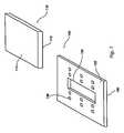
- FIGS. 1 through 5illustrate a method of making a semiconductor assembly according to a first embodiment of the present invention, in which:
- FIG. 1is a simplified perspective view of a semiconductor die and a carrier substrate in an unattached position according to the present invention
- FIG. 2is a simplified cross-sectional view of a semiconductor die attached face down to a carrier substrate with conductive bumps therebetween to form a semiconductor assembly, according to the present invention
- FIG. 3is a simplified cross-sectional view of the semiconductor assembly as shown in FIG. 2 with filler material between the semiconductor die and the carrier substrate and bond wires extending from the semiconductor die to the carrier substrate, according to the present invention
- FIG. 4is a simplified cross-sectional view of the semiconductor assembly as shown in FIG. 3 with an encapsulation material encapsulating the bond wires and the semiconductor die, according to the present invention
- FIG. 5is a simplified cross-sectional view of the semiconductor assembly as shown in FIG. 4 , wherein the semiconductor assembly is attached to a printed circuit board, according to the present invention
- FIGS. 6 through 8illustrate a method of making a semiconductor assembly according to a second embodiment of the present invention, wherein FIG. 6 is a simplified perspective view of a die and a carrier substrate in an unattached position, wherein the carrier substrate includes a plurality of openings therein, according to the present invention, wherein
- FIG. 7is a simplified cross-sectional view of a semiconductor die attached face down to a carrier substrate with conductive bumps and bond wires extending therebetween forming a semiconductor assembly, according to the present invention
- FIG. 8is a simplified cross-sectional view of the semiconductor assembly as shown in FIG. 7 , wherein the semiconductor assembly is attached to a printed circuit board, according to the present invention
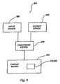
- FIG. 9is a simplified block diagram of the semiconductor assembly of the present invention integrated in a computer system.
- FIG. 1An exemplary first embodiment of the method and apparatus incorporating teachings of a semiconductor assembly is shown in drawing FIGS. 1 through 5 .
- the semiconductor die 110includes an active surface 112 and a back surface 114 and is generally rectangular in shape.
- the semiconductor die 110is typically made of a semiconductor material, such as germanium, lead sulfide, silicon, gallium arsenide and silicon carbide, but is not limited to such materials.
- the semiconductor die 110includes integrated circuitry therein and bond pads 132 located substantially centrally in one or more rows on the active surface 112 thereof and, in addition, bond pads 132 located in peripheral outer portions on the active surface 112 thereof (see FIG. 2 ).
- the carrier substrate 120includes a first surface 122 and a second surface 124 with an opening 126 therein.
- the opening 126is centrally located in the carrier substrate 120 and extends through and from the first surface 122 to the second surface 124 of the carrier substrate 120 .
- the carrier substrate 120may be any type of substrate or interposer and is typically made of various materials, such as ceramic, silicone, glass, and combinations thereof.
- the carrier substrate 120includes bond pads 128 on the first surface 122 and the second surface 124 thereof (see FIGS. 1 and 2 ).
- FIG. 2A simplified cross-sectional view of a semiconductor assembly 100 and, more specifically, of the semiconductor die 110 attached to the carrier substrate 120 is depicted in drawing FIG. 2 .
- the semiconductor die 110with its active surface 112 face down, is attached to the first surface 122 of the carrier substrate 120 with conductive bumps 130 sandwiched therebetween.
- the conductive bumps 130are electrically interconnected and aligned between bond pads 129 on the first surface 122 of the carrier substrate 120 and bond pads 132 at peripheral outer portions of the semiconductor die's active surface 112 .
- the semiconductor die 110is aligned such that centrally located bond pads 132 on the semiconductor die 110 are exposed through the opening 126 of the carrier substrate 120 .
- the carrier substrate 120 or the semiconductor die 110may then be aligned and attached to the pre-attached conductive bumps 130 on either the semiconductor die 110 or carrier substrate 120 using conventional aligning techniques known in the art.
- the attached assemblyis then heated to a suitable predetermined temperature, determined by the material properties of the conductive bumps 130 , to reflow the conductive bumps 130 to bond and electrically interconnect the semiconductor die 110 and carrier substrate 120 .
- drawing FIG. 2depicts interconnect bumps 134 , which are generally larger than the conductive bumps 130 , attached to the second surface 124 of the carrier substrate 120 .
- the interconnect bumps 134are preferably pre-attached to the carrier substrate 120 .
- the interconnect bumps 134are made for attaching the semiconductor assembly to another substrate such as a printed circuit board (see FIG. 5 ), which will be discussed in further detail hereafter.
- the conductive bumps 130are preferably shaped as balls, but may be shaped as pillars, columns, and/or studs.
- the conductive bumps 130may be formed of any known conductive material or alloy thereof, such as solder, lead, tin, copper, silver and/or gold and conductive polymers and/or conductive composites.
- the conductive bumps 130may include a core having layers thereon utilizing such materials and/or alloys thereof. As such, the conductive bumps 130 act as electrical interconnections between the semiconductor die 110 and the carrier substrate 120 .
- the conductive bumps 130preferably employed are solder balls, stud bumps, and/or bumps formed from a z-axis conductive material.
- the previously set forth interconnect bumps 134may have the same physical and electrical characteristics as the conductive bumps 130 .
- the underfill processmay be accomplished by employing methods of injecting, dispensing or flowing a filler material 144 or any known method to those skilled in the art.
- such methodsmay include applying the filler material 144 in the gap between the semiconductor die 110 and the carrier substrate 120 and allowing the filler material 144 to fill the gap by capillary action and/or pressure flow.
- the filler material 144is not required, it is preferred so as to protect the conductive bumps 130 from the environment.
- the semiconductor die 110is wire bonded to the carrier substrate 120 .
- bond wires 140are made to extend through the opening 126 and attach between the centrally located bond pads 132 on the semiconductor die 110 exposed through the opening 126 and the bond pads 128 on the second surface 124 of the carrier substrate 120 .
- the wire bondingmay be employed by any known method such as ultrasonic bonding, thermocompression bonding and thermosonic bonding. Therefore, with this arrangement as depicted in drawing FIG. 3 , the semiconductor die 110 is electrically interconnected to the carrier substrate 120 by both the bond wires 140 and the conductive bumps 130 .
- vulnerable components in the semiconductor assemblyare sealed in an encapsulation material 150 such as a resin.
- an encapsulation material 150such as a resin.
- the bond wires 140 and/or exposed portions of the semiconductor die 110are preferably sealed with an encapsulation material 150 .
- the encapsulation material 150is typically disposed over the semiconductor assembly through a transfer molding process as known in the art.
- the filler material 144may be replaced by the encapsulation material 150 , as the encapsulation material 150 may fill the gap between the semiconductor die 110 and the carrier substrate 120 .
- the encapsulation material 150should be applied to at least seal the bond wires 140 and their interconnections.
- a glob top processas known in the art.
- a glob top processmay be employed by disposing the encapsulation material 150 into the opening 126 of the carrier substrate 120 to, thereby, seal the bond wires 140 and each of their respective interconnections on the semiconductor die 110 and the carrier substrate 120 .
- the assemblymay be attached to a printed circuit board 160 with the interconnect bumps 134 located between the second surface 124 of the carrier substrate 120 and the upper surface of the printed circuit board 160 as shown in drawing FIG. 5 .
- a second embodiment of the present inventionis depicted in drawing FIGS. 6 through 8 .
- the second embodimentincludes a semiconductor die 210 having an active surface 212 and a back surface 214 and a carrier substrate 220 having a first and second surface 222 and 224 , as in the first embodiment.
- the carrier substrate 220includes multiple openings 226 .
- the openings 226are preferably located proximate a periphery of the carrier substrate 220 or, rather, the openings 226 are sized and configured to substantially outline the semiconductor die periphery when the semiconductor die 210 is attached to the carrier substrate 220 .
- Each of the openings 226extends through the first surface 222 of the carrier substrate 220 to the second surface 224 of the carrier substrate 220 .
- Adjacent openings 226 of the substrate 220 of the at least one semiconductor assembly 210may extend proximate more than one side of a periphery of the substrate 220 (shown in dashed lines).
- the semiconductor die 210includes bond pads 232 on its active surface 212 .
- the bond pads 232 interconnecting with the conductive bumps 230are arranged centrally on the active surface 212 of the semiconductor die 210 and the bond pads 232 interconnecting with the bond wires 240 are aligned proximate the die periphery on the active surface 212 of the semiconductor die 210 .
- the semiconductor die 210is attached to the first surface 222 of the carrier substrate 220 . Similar to the first embodiment, the semiconductor die 210 is electrically interconnected to the carrier substrate 220 with conductive bumps 230 and bond wires 240 . However, the bond wires 240 are interconnected to bond pads 232 on the semiconductor die 210 at a periphery portion of the active surface 212 of the semiconductor die 210 . The bond wires 240 extend from the periphery portion of the active surface 212 through the openings 226 of the carrier substrate 220 to bond pads 228 on the second surface 224 of the carrier substrate 220 .
- the semiconductor die 210 and the carrier substrate 220are electrically interconnected by both the conductive bumps 230 and the bond wires 240 .
- the second embodimentmay include a filler material 244 and an encapsulation material 250 for encapsulating particular components of the semiconductor assembly 200 .
- the second embodimentalso includes interconnect bumps 234 on the second surface 224 of the carrier substrate 220 . With the interconnect bumps 234 , the semiconductor assembly 200 may be electrically interconnected to another substrate such as a printed circuit board 260 , as shown in drawing FIG. 8 .
- both the conductive bumps 230 and the bond wires 240share in the electrical interconnection between the semiconductor die 210 and the carrier substrate 220 .
- the present inventionprovides that the conductive bumps 230 include the power and ground connections and the difficult signal routes between the semiconductor die 210 and the carrier substrate 220 .
- both the conductive bumps 230 and the plurality of bond wires 240include a portion of the signal routing between the semiconductor die 210 and the carrier substrate 220 .
- the conductive bumps 230 and the bond wires 240are arranged to share in the electrical interconnection between the semiconductor die 210 and substrate 220 , there is additional space on the semiconductor die 210 for bond pads used for bond wires 240 and/or the additional space allows for a smaller die size. Furthermore, since the present invention requires conductive bumps 230 for only the power and ground connections and the difficult signal routing connections, the number of conductive bumps 230 is limited, thereby providing a more efficient aligning process with the bond pads 228 of the substrate 220 without the high probability for alignment error as found in conventional flip-chip aligning processes.
- the semiconductor assembly 100 of the first embodiment and the semiconductor assembly 200 of the second embodimentare each contemplated for use within a computer system.
- the semiconductor assembly 100 , 200 of the present inventioncan be used to clear the memory devices of a computer system or to implement a memory storage device of a computer system.
- Other types of implementationmay incorporate a processing unit that provides the main functions of operation within either a computer system or any preferable implantation processing capabilities such as a video card or any other preferable device.
- Drawing FIG. 9is an example in which the semiconductor assembly 100 , 200 of the present invention may be integrated into a computer system.
- the semiconductor assembly 100 , 200 of the present inventionmounted to a circuit board 360 in a computer system 300 .
- the circuit board 360is connected to a processor device 370 which communicates with an input device 380 and an output device 390 .
- the input device 380may be a keyboard, mouse, joystick or any other computer input device.
- the output device 390may be a monitor, printer or storage device, such as a disk drive, or any other output device.
- the processor device 370may be, but is not limited to, a microprocessor or a circuit card including hardware for processing computer instructions. Additional preferable structure for the computer system 300 would be readily apparent to those skilled in the art.
Landscapes
- Engineering & Computer Science (AREA)
- Microelectronics & Electronic Packaging (AREA)
- Computer Hardware Design (AREA)
- Power Engineering (AREA)
- Physics & Mathematics (AREA)
- Condensed Matter Physics & Semiconductors (AREA)
- General Physics & Mathematics (AREA)
- Manufacturing & Machinery (AREA)
- Wire Bonding (AREA)
- Encapsulation Of And Coatings For Semiconductor Or Solid State Devices (AREA)
Abstract
Description
- This application is a continuation of application Ser. No. 10/792,229, filed Mar. 3, 2004, pending, which is a divisional of application Ser. No. 10/092,276, filed Mar. 5, 2002, now U.S. Pat. No. 6,744,137, issued Jun. 1, 2004, which is a divisional of application Ser. No. 09/863,245, filed May 21, 2001, now U.S. Pat. No. 6,528,408, issued Mar. 4, 2003.
- 1. Field of the Invention
- The present invention relates to a method and apparatus for interconnecting a semiconductor die or semiconductor device to a carrier substrate. In particular, the present invention relates to a method and apparatus for attaching a semiconductor die face down to a carrier substrate so that the semiconductor die is electrically interconnected to the carrier substrate using both conductive bumps and bond wires.
- 2. State of the Art
- Well-known techniques typically used for bonding and electrically connecting a semiconductor die to a substrate, such as a printed circuit board, interposer, or carrier substrate, are flip-chip attachment, wire bonding, and tape automated bonding (“TAB”). Such techniques are known in the art as Chip-On-Board (“COB”) or, otherwise, Board-On-Chip (“BOC”) technology.
- Flip-chip attachment generally consists of attaching an active surface of a semiconductor die to a substrate with a plurality of conductive bumps therebetween. Each conductive bump must align and correspond with respective bond pads on the substrate and the semiconductor die to provide electrical interconnection therebetween. The semiconductor die is bonded to the substrate by reflowing the conductive bumps, after which an underfill material is typically disposed between the semiconductor die and the substrate for environmental protection and to enhance the attachment of the semiconductor die to the substrate.
- Although flip-chip packages exhibit excellent response time, from a production standpoint, flip-chip attachment has several challenges due to the numerous amount of conductive bumps required. In particular, if the substrate connection arrangement is not a mirror image of the conductive bumps on the semiconductor die, electrically connecting the semiconductor die to the substrate is impossible. Such a challenge is exemplified by the methods disclosed in United States patents U.S. Pat. No. 3,811,186; U.S. Pat. No. 4,940,181; U.S. Pat. No. 5,477,086; and U.S. Pat. No. 5,329,423 for self aligning the conductive bumps.
- Turning to the BOC techniques of wire bonding and TAB, the semiconductor die is directly attached to the surface of a substrate, i.e., printed circuit board, interposer, or carrier substrate, with an appropriate adhesive, such as an epoxy or adhesive tape. The die may be oriented either face up or face down (with its active surface and bond pads either up or down with respect to the circuit board) for wire bonding. A plurality of bond wires is then discretely attached to each bond pad on the semiconductor die and extends to a corresponding bond pad on the substrate. The bond wires are generally attached through one of three industry-standard wire bonding techniques: ultrasonic bonding (using a combination of pressure and ultrasonic vibration bursts to form a metallurgical cold weld); thermocompression bonding (using a combination of pressure and elevated temperature to form a weld); and thermosonic bonding (using a combination of pressure, elevated temperature, and ultrasonic vibration bursts). TAB is generally employed to connect ends of metal leads carried on an insulating tape such as a polyimide respectively to the bond pads on the semiconductor die and the bond pads on the printed circuit board. For both wire bonding and TAB techniques, an encapsulant is typically used to cover the bond wires and metal tape leads to prevent contamination.
- Among the different methods of wire bonding a semiconductor die to a substrate, one method includes adhesively attaching a semiconductor die to a substrate in the facedown orientation. In this orientation, the active surface of the die is adhesively attached to a portion of the substrate, i.e., printed circuit board, interposer, or carrier substrate, etc., having one or more wire bonding openings therein so that bond wires can extend through the opening from bond pads on the substrate to bond pads on the active surface of the die. For example, see U.S. Pat. No. 5,719,440, assigned to the assignee of the present invention, which discloses the die adhesively attached face down to a substrate with wire bonding through an opening in the substrate.
- This facedown semiconductor die orientation is advantageous by allowing shorter wire bonds resulting in less potential for interwire contact and shorting. However, problems with this arrangement include moisture becoming trapped in the adhesive between the semiconductor die and substrate, often resulting in the package cracking when the moisture turns to steam as the package is exposed to high temperatures. Other problems include managing the power and ground wire bond interconnections and the difficult routing signals from both an integrity and reliability standpoint and, additionally, the standpoint of meeting the demands of available “real estate.” In other words, since the facedown semiconductor die orientation is limited to the one or more openings in the substrate which expose the active surface of the semiconductor die for wire bond interconnections, the space on the active surface exposed by the substrate opening severely limits the number of possible interconnections that may be made via the wire bonds. Further, the wire bonds necessary for the power and ground are larger due to the increased amount of current running therethrough, thus, further compounding the available space problem for each of the wire bond interconnections.
- Therefore, in light of the foregoing, it would be advantageous to provide a semiconductor package with increased integrity and reliability as well as to better manage the available space for wire bonding in a facedown-oriented semiconductor die. It would also be advantageous to provide a semiconductor package that substantially prevents trapping moisture therein.
- The present invention relates to a semiconductor assembly and is directed to the interconnections between a semiconductor die attached face down to a carrier substrate.
- In a preferred embodiment of the present invention, the semiconductor assembly includes a carrier substrate having a first surface and a second surface with at least one opening in the carrier substrate which extends from the first surface to the second surface. The semiconductor die includes an active surface and a back surface, wherein the semiconductor die is attached face down to the first surface of the carrier substrate with conductive bumps therebetween. In addition, a plurality of bond wires is attached through the at least one opening in the carrier substrate between the active surface of the die and the second surface of the carrier substrate.
- In one embodiment, the at least one opening is a single opening centrally located in the carrier substrate. The semiconductor die is attached face down over the opening so that centrally located bond pads on the semiconductor die are exposed through the opening and outer bond pads on the die are mirrored with bond pads on the first surface of the carrier substrate with the conductive bumps between such mirrored bond pads. With this arrangement, the plurality of bond wires is attached through the single opening centrally located in the carrier substrate between the centrally located bond pads on the active surface of the semiconductor die and the bond pads on the second surface of the carrier substrate. Therefore, the semiconductor die is electrically interconnected to the carrier substrate by both the conductive bumps and the bond wires.
- In a second embodiment, the at least one opening is a plurality of openings located proximate a periphery of the carrier substrate. The semiconductor die is attached face down to the carrier substrate so that peripheral bond pads on the semiconductor die are exposed through the plurality of openings and centrally located bond pads are mirrored with bond pads on the first surface of the carrier substrate with the conductive bumps between such mirrored bond pads. With this arrangement, the plurality of bond wires is attached through the plurality of openings located proximate the periphery of the carrier substrate between the peripheral bond pads on the semiconductor die and the bond pads on the second surface of the carrier substrate. Therefore, in the second embodiment, the semiconductor die is electrically interconnected to the carrier substrate by both the conductive bumps and the bond wires.
- According to the present invention, both the conductive bumps and the bond wires share in the electrical interconnection between the semiconductor die and the carrier substrate. In particular, the present invention provides that the conductive bumps include power and ground connections between the semiconductor die and the carrier substrate. Further, the conductive bumps and the plurality of bond wires each collectively include a portion of the signal routing between the semiconductor die and the carrier substrate. By arranging the conductive bumps and the bond wires to share in the electrical interconnection between the semiconductor die and substrate, there is more space on the die for bond pads and/or this arrangement allows for a smaller die size.
- In the present invention, the semiconductor assembly may include a filler material disposed around the conductive bumps and between the semiconductor die and carrier substrate, which may be applied by injecting, dispensing or flowing the filler material from a dispenser. The semiconductor assembly includes a sealant or encapsulation material to at least encapsulate the plurality of bond wires. The encapsulation material may also substantially encapsulate exposed portions of the semiconductor die. Such encapsulation material may be formed on the semiconductor assembly by a transfer molding process or by a glob top process. In a transfer molding process, the encapsulation material may act as the filler material, depending on the characteristics of the encapsulation material, such as the viscosity.
- In the present invention, the conductive bumps are electrical interconnections between the semiconductor die and the carrier substrate. As such, the conductive bumps may comprise any conductive material such as solder balls and/or z-axis conductive material. The conductive bumps may include layers having a core and a shell, in which the core may be a nonconductive polymer. The shell and core may also include conductive polymers, metals, and/or alloys. The conductive bumps may also be in the form of a stud bump or a column.
- In another aspect of the present invention, the semiconductor assembly includes interconnect bumps on the second surface of the carrier substrate for electrical interconnection with a printed circuit board. Similar to the conductive bumps, the interconnect bumps may include any conductive material such as solder balls and/or z-axis material. The interconnect bumps may include layers having a core and a shell, in which the core may be a nonconductive polymer. The shell and core may also include conductive polymers, metals, and/or alloys. The interconnect bumps may also be in the form of a stud bump, formed from the wire bonding material, or a column.
- In another aspect of the present invention, the semiconductor assembly is mounted to a circuit board in a computer or a computer system. In the computer system, the circuit board is electrically connected to a processor device which electrically communicates with an input device and an output device.
- Other features and advantages of the present invention will become apparent to those of skill in the art through a consideration of the ensuing description, the accompanying drawings and the appended claims.
- While the specification concludes with claims particularly pointing out and distinctly claiming that which is regarded as the present invention, the advantages of this invention may be ascertained from the following description of the invention when read in conjunction with the accompanying drawings.
FIGS. 1 through 5 illustrate a method of making a semiconductor assembly according to a first embodiment of the present invention, in which:FIG. 1 is a simplified perspective view of a semiconductor die and a carrier substrate in an unattached position according to the present invention;FIG. 2 is a simplified cross-sectional view of a semiconductor die attached face down to a carrier substrate with conductive bumps therebetween to form a semiconductor assembly, according to the present invention;FIG. 3 is a simplified cross-sectional view of the semiconductor assembly as shown inFIG. 2 with filler material between the semiconductor die and the carrier substrate and bond wires extending from the semiconductor die to the carrier substrate, according to the present invention;FIG. 4 is a simplified cross-sectional view of the semiconductor assembly as shown inFIG. 3 with an encapsulation material encapsulating the bond wires and the semiconductor die, according to the present invention;FIG. 5 is a simplified cross-sectional view of the semiconductor assembly as shown inFIG. 4 , wherein the semiconductor assembly is attached to a printed circuit board, according to the present invention;FIGS. 6 through 8 illustrate a method of making a semiconductor assembly according to a second embodiment of the present invention, whereinFIG. 6 is a simplified perspective view of a die and a carrier substrate in an unattached position, wherein the carrier substrate includes a plurality of openings therein, according to the present invention, whereinFIG. 7 is a simplified cross-sectional view of a semiconductor die attached face down to a carrier substrate with conductive bumps and bond wires extending therebetween forming a semiconductor assembly, according to the present invention, and whereinFIG. 8 is a simplified cross-sectional view of the semiconductor assembly as shown inFIG. 7 , wherein the semiconductor assembly is attached to a printed circuit board, according to the present invention; andFIG. 9 is a simplified block diagram of the semiconductor assembly of the present invention integrated in a computer system.- Preferred embodiments of the present invention will be hereinafter described with reference to the accompanying drawings. It should be understood that the illustrations are not meant to be actual views of any particular apparatus and/or method, but are merely idealized representations which are employed to more clearly and fully depict the present invention than would otherwise be possible. Additionally, elements and features common between the figures retain the same numerical designation.
- An exemplary first embodiment of the method and apparatus incorporating teachings of a semiconductor assembly is shown in drawing
FIGS. 1 through 5 . Depicted in drawingFIG. 1 is a simplified perspective view of asemiconductor die 110 and acarrier substrate 120 in an unattached position. The semiconductor die110 includes anactive surface 112 and aback surface 114 and is generally rectangular in shape. The semiconductor die110 is typically made of a semiconductor material, such as germanium, lead sulfide, silicon, gallium arsenide and silicon carbide, but is not limited to such materials. The semiconductor die110 includes integrated circuitry therein andbond pads 132 located substantially centrally in one or more rows on theactive surface 112 thereof and, in addition,bond pads 132 located in peripheral outer portions on theactive surface 112 thereof (seeFIG. 2 ). - The
carrier substrate 120 includes afirst surface 122 and asecond surface 124 with anopening 126 therein. Theopening 126 is centrally located in thecarrier substrate 120 and extends through and from thefirst surface 122 to thesecond surface 124 of thecarrier substrate 120. Thecarrier substrate 120 may be any type of substrate or interposer and is typically made of various materials, such as ceramic, silicone, glass, and combinations thereof. Thecarrier substrate 120 includesbond pads 128 on thefirst surface 122 and thesecond surface 124 thereof (seeFIGS. 1 and 2 ). - A simplified cross-sectional view of a
semiconductor assembly 100 and, more specifically, of the semiconductor die110 attached to thecarrier substrate 120 is depicted in drawingFIG. 2 . In particular, the semiconductor die110, with itsactive surface 112 face down, is attached to thefirst surface 122 of thecarrier substrate 120 withconductive bumps 130 sandwiched therebetween. Theconductive bumps 130 are electrically interconnected and aligned betweenbond pads 129 on thefirst surface 122 of thecarrier substrate 120 andbond pads 132 at peripheral outer portions of the semiconductor die'sactive surface 112. Further, the semiconductor die110 is aligned such that centrally locatedbond pads 132 on the semiconductor die110 are exposed through theopening 126 of thecarrier substrate 120. - Preceding such alignment and attachment of the semiconductor die110 and the
carrier substrate 120, it is preferable to pre-attach theconductive bumps 130 to the respective bond pads of either the semiconductor die110 or thecarrier substrate 120. In this manner, thecarrier substrate 120 or the semiconductor die110 (without the pre-attached conductive bumps) may then be aligned and attached to the pre-attachedconductive bumps 130 on either the semiconductor die110 orcarrier substrate 120 using conventional aligning techniques known in the art. The attached assembly is then heated to a suitable predetermined temperature, determined by the material properties of theconductive bumps 130, to reflow theconductive bumps 130 to bond and electrically interconnect the semiconductor die110 andcarrier substrate 120. - In addition, drawing
FIG. 2 depicts interconnect bumps134, which are generally larger than theconductive bumps 130, attached to thesecond surface 124 of thecarrier substrate 120. For alignment purposes, the interconnect bumps134 are preferably pre-attached to thecarrier substrate 120. The interconnect bumps134 are made for attaching the semiconductor assembly to another substrate such as a printed circuit board (seeFIG. 5 ), which will be discussed in further detail hereafter. - The
conductive bumps 130 are preferably shaped as balls, but may be shaped as pillars, columns, and/or studs. Theconductive bumps 130 may be formed of any known conductive material or alloy thereof, such as solder, lead, tin, copper, silver and/or gold and conductive polymers and/or conductive composites. Theconductive bumps 130 may include a core having layers thereon utilizing such materials and/or alloys thereof. As such, theconductive bumps 130 act as electrical interconnections between the semiconductor die110 and thecarrier substrate 120. Theconductive bumps 130 preferably employed are solder balls, stud bumps, and/or bumps formed from a z-axis conductive material. In addition, the previously set forth interconnect bumps134 may have the same physical and electrical characteristics as theconductive bumps 130. - With the semiconductor die110 attached to the
carrier substrate 120, the semiconductor assembly is prepared for an underfill process and wire bonding, as shown in drawingFIG. 3 . The underfill process may be accomplished by employing methods of injecting, dispensing or flowing afiller material 144 or any known method to those skilled in the art. For example, such methods may include applying thefiller material 144 in the gap between the semiconductor die110 and thecarrier substrate 120 and allowing thefiller material 144 to fill the gap by capillary action and/or pressure flow. Although thefiller material 144 is not required, it is preferred so as to protect theconductive bumps 130 from the environment. - In addition, as shown in drawing
FIG. 3 , the semiconductor die110 is wire bonded to thecarrier substrate 120. In particular,bond wires 140 are made to extend through theopening 126 and attach between the centrally locatedbond pads 132 on the semiconductor die110 exposed through theopening 126 and thebond pads 128 on thesecond surface 124 of thecarrier substrate 120. The wire bonding may be employed by any known method such as ultrasonic bonding, thermocompression bonding and thermosonic bonding. Therefore, with this arrangement as depicted in drawingFIG. 3 , the semiconductor die110 is electrically interconnected to thecarrier substrate 120 by both thebond wires 140 and theconductive bumps 130. - As shown in drawing
FIG. 4 , vulnerable components in the semiconductor assembly are sealed in anencapsulation material 150 such as a resin. In particular, after wire bonding the semiconductor die110 to thecarrier substrate 120, thebond wires 140 and/or exposed portions of the semiconductor die110 are preferably sealed with anencapsulation material 150. Theencapsulation material 150 is typically disposed over the semiconductor assembly through a transfer molding process as known in the art. Depending on the characteristics of the encapsulation material, i.e., viscosity, used in a transfer molding process, thefiller material 144 may be replaced by theencapsulation material 150, as theencapsulation material 150 may fill the gap between the semiconductor die110 and thecarrier substrate 120. However, at a minimum, theencapsulation material 150 should be applied to at least seal thebond wires 140 and their interconnections. - Other methods for providing the
encapsulation material 150 or resin around thebond wires 140 may be applied such as a glob top process as known in the art. For example, such a glob top process may be employed by disposing theencapsulation material 150 into theopening 126 of thecarrier substrate 120 to, thereby, seal thebond wires 140 and each of their respective interconnections on the semiconductor die110 and thecarrier substrate 120. - After the
encapsulation material 150 has been formed on thesemiconductor assembly 100, the assembly may be attached to a printedcircuit board 160 with the interconnect bumps134 located between thesecond surface 124 of thecarrier substrate 120 and the upper surface of the printedcircuit board 160 as shown in drawingFIG. 5 . - A second embodiment of the present invention is depicted in drawing
FIGS. 6 through 8 . The second embodiment, as illustrated in drawingFIG. 6 , includes asemiconductor die 210 having anactive surface 212 and aback surface 214 and acarrier substrate 220 having a first andsecond surface carrier substrate 220 includesmultiple openings 226. In particular, theopenings 226 are preferably located proximate a periphery of thecarrier substrate 220 or, rather, theopenings 226 are sized and configured to substantially outline the semiconductor die periphery when the semiconductor die210 is attached to thecarrier substrate 220. Each of theopenings 226 extends through thefirst surface 222 of thecarrier substrate 220 to thesecond surface 224 of thecarrier substrate 220.Adjacent openings 226 of thesubstrate 220 of the at least onesemiconductor assembly 210 may extend proximate more than one side of a periphery of the substrate220 (shown in dashed lines). - Depicted in drawing
FIG. 7 is thesemiconductor assembly 200 of the second embodiment. As shown, the semiconductor die210 includesbond pads 232 on itsactive surface 212. Specifically, thebond pads 232 interconnecting with theconductive bumps 230 are arranged centrally on theactive surface 212 of the semiconductor die210 and thebond pads 232 interconnecting with thebond wires 240 are aligned proximate the die periphery on theactive surface 212 of the semiconductor die210. - The semiconductor die210, with its
active surface 212 face down, is attached to thefirst surface 222 of thecarrier substrate 220. Similar to the first embodiment, the semiconductor die210 is electrically interconnected to thecarrier substrate 220 withconductive bumps 230 andbond wires 240. However, thebond wires 240 are interconnected to bondpads 232 on the semiconductor die210 at a periphery portion of theactive surface 212 of the semiconductor die210. Thebond wires 240 extend from the periphery portion of theactive surface 212 through theopenings 226 of thecarrier substrate 220 tobond pads 228 on thesecond surface 224 of thecarrier substrate 220. With this arrangement, the semiconductor die210 and thecarrier substrate 220 are electrically interconnected by both theconductive bumps 230 and thebond wires 240. As in the first embodiment, the second embodiment may include afiller material 244 and anencapsulation material 250 for encapsulating particular components of thesemiconductor assembly 200. Further, the second embodiment also includes interconnect bumps234 on thesecond surface 224 of thecarrier substrate 220. With the interconnect bumps234, thesemiconductor assembly 200 may be electrically interconnected to another substrate such as a printedcircuit board 260, as shown in drawingFIG. 8 . - According to the present invention, both the
conductive bumps 230 and thebond wires 240 share in the electrical interconnection between the semiconductor die210 and thecarrier substrate 220. In particular, the present invention provides that theconductive bumps 230 include the power and ground connections and the difficult signal routes between the semiconductor die210 and thecarrier substrate 220. In this manner, both theconductive bumps 230 and the plurality ofbond wires 240 include a portion of the signal routing between the semiconductor die210 and thecarrier substrate 220. Therefore, by arranging theconductive bumps 230 and thebond wires 240 to share in the electrical interconnection between the semiconductor die210 andsubstrate 220, there is additional space on the semiconductor die210 for bond pads used forbond wires 240 and/or the additional space allows for a smaller die size. Furthermore, since the present invention requiresconductive bumps 230 for only the power and ground connections and the difficult signal routing connections, the number ofconductive bumps 230 is limited, thereby providing a more efficient aligning process with thebond pads 228 of thesubstrate 220 without the high probability for alignment error as found in conventional flip-chip aligning processes. - The
semiconductor assembly 100 of the first embodiment and thesemiconductor assembly 200 of the second embodiment are each contemplated for use within a computer system. For example, thesemiconductor assembly FIG. 9 is an example in which thesemiconductor assembly - As illustrated in block diagram form in drawing
FIG. 9 , there is thesemiconductor assembly circuit board 360 in acomputer system 300. In thecomputer system 300, thecircuit board 360 is connected to aprocessor device 370 which communicates with aninput device 380 and anoutput device 390. Theinput device 380 may be a keyboard, mouse, joystick or any other computer input device. Theoutput device 390 may be a monitor, printer or storage device, such as a disk drive, or any other output device. Theprocessor device 370 may be, but is not limited to, a microprocessor or a circuit card including hardware for processing computer instructions. Additional preferable structure for thecomputer system 300 would be readily apparent to those skilled in the art. - The above descriptions and drawings are only illustrative of preferred embodiments which achieve the objects, features and advantages of the present invention, and it is not intended that the present invention be limited thereto. Any modification of the present invention which comes within the spirit and scope of the following claims is considered part of the present invention.
Claims (58)
Priority Applications (1)
| Application Number | Priority Date | Filing Date | Title |
|---|---|---|---|
| US11/523,915US7629686B2 (en) | 2001-05-21 | 2006-09-20 | Bumped die and wire bonded board-on-chip package |
Applications Claiming Priority (4)
| Application Number | Priority Date | Filing Date | Title |
|---|---|---|---|
| US09/863,245US6528408B2 (en) | 2001-05-21 | 2001-05-21 | Method for bumped die and wire bonded board-on-chip package |
| US10/092,276US6744137B2 (en) | 2001-05-21 | 2002-03-05 | Bumped die and wire bonded board-on-chip package |
| US10/792,229US7116001B2 (en) | 2001-05-21 | 2004-03-03 | Bumped die and wire bonded board-on-chip package |
| US11/523,915US7629686B2 (en) | 2001-05-21 | 2006-09-20 | Bumped die and wire bonded board-on-chip package |
Related Parent Applications (1)
| Application Number | Title | Priority Date | Filing Date |
|---|---|---|---|
| US10/792,229ContinuationUS7116001B2 (en) | 2001-05-21 | 2004-03-03 | Bumped die and wire bonded board-on-chip package |
Publications (2)
| Publication Number | Publication Date |
|---|---|
| US20070013084A1true US20070013084A1 (en) | 2007-01-18 |
| US7629686B2 US7629686B2 (en) | 2009-12-08 |
Family
ID=25340667
Family Applications (6)
| Application Number | Title | Priority Date | Filing Date |
|---|---|---|---|
| US09/863,245Expired - LifetimeUS6528408B2 (en) | 2001-05-21 | 2001-05-21 | Method for bumped die and wire bonded board-on-chip package |
| US10/092,276Expired - LifetimeUS6744137B2 (en) | 2001-05-21 | 2002-03-05 | Bumped die and wire bonded board-on-chip package |
| US10/366,943Expired - LifetimeUS6682998B2 (en) | 2001-05-21 | 2003-02-14 | Methods for bumped die and wire bonded board-on-chip package |
| US10/792,229Expired - LifetimeUS7116001B2 (en) | 2001-05-21 | 2004-03-03 | Bumped die and wire bonded board-on-chip package |
| US10/793,564Expired - LifetimeUS7115990B2 (en) | 2001-05-21 | 2004-03-04 | Bumped die and wire bonded board-on-chip package |
| US11/523,915Expired - LifetimeUS7629686B2 (en) | 2001-05-21 | 2006-09-20 | Bumped die and wire bonded board-on-chip package |
Family Applications Before (5)
| Application Number | Title | Priority Date | Filing Date |
|---|---|---|---|
| US09/863,245Expired - LifetimeUS6528408B2 (en) | 2001-05-21 | 2001-05-21 | Method for bumped die and wire bonded board-on-chip package |
| US10/092,276Expired - LifetimeUS6744137B2 (en) | 2001-05-21 | 2002-03-05 | Bumped die and wire bonded board-on-chip package |
| US10/366,943Expired - LifetimeUS6682998B2 (en) | 2001-05-21 | 2003-02-14 | Methods for bumped die and wire bonded board-on-chip package |
| US10/792,229Expired - LifetimeUS7116001B2 (en) | 2001-05-21 | 2004-03-03 | Bumped die and wire bonded board-on-chip package |
| US10/793,564Expired - LifetimeUS7115990B2 (en) | 2001-05-21 | 2004-03-04 | Bumped die and wire bonded board-on-chip package |
Country Status (1)
| Country | Link |
|---|---|
| US (6) | US6528408B2 (en) |
Cited By (3)
| Publication number | Priority date | Publication date | Assignee | Title |
|---|---|---|---|---|
| US20080029871A1 (en)* | 2006-08-04 | 2008-02-07 | Hong-Kweun Kim | Interposer and semiconductor package using the same |
| US20090206492A1 (en)* | 2008-02-14 | 2009-08-20 | Elpida Memory, Inc. | Semiconductor device |
| CN100573863C (en)* | 2008-04-30 | 2009-12-23 | 日月光半导体制造股份有限公司 | Flip chip package structure and method for manufacturing the same |
Families Citing this family (97)
| Publication number | Priority date | Publication date | Assignee | Title |
|---|---|---|---|---|
| US6414391B1 (en)* | 1998-06-30 | 2002-07-02 | Micron Technology, Inc. | Module assembly for stacked BGA packages with a common bus bar in the assembly |
| DE19954888C2 (en)* | 1999-11-15 | 2002-01-10 | Infineon Technologies Ag | Packaging for a semiconductor chip |
| US6577018B1 (en)* | 2000-08-25 | 2003-06-10 | Micron Technology, Inc. | Integrated circuit device having reduced bow and method for making same |
| TWI313507B (en)* | 2002-10-25 | 2009-08-11 | Megica Corporatio | Method for assembling chips |
| US6528408B2 (en)* | 2001-05-21 | 2003-03-04 | Micron Technology, Inc. | Method for bumped die and wire bonded board-on-chip package |
| BR0102842A (en)* | 2001-05-22 | 2003-03-05 | Brasil Compressores Sa | Linear motor blade and blade arrangement |
| DE10127009A1 (en)* | 2001-06-05 | 2002-12-12 | Infineon Technologies Ag | Plastic housing used for packing semiconductor chips comprises semiconductor chips arranged in lines and gaps |
| SG102637A1 (en)* | 2001-09-10 | 2004-03-26 | Micron Technology Inc | Bow control in an electronic package |
| US8977284B2 (en) | 2001-10-04 | 2015-03-10 | Traxcell Technologies, LLC | Machine for providing a dynamic data base of geographic location information for a plurality of wireless devices and process for making same |
| JP2003152021A (en)* | 2001-11-09 | 2003-05-23 | Seiko Epson Corp | Semiconductor device and its manufacturing method, circuit board, and electronic equipment |
| US7109588B2 (en)* | 2002-04-04 | 2006-09-19 | Micron Technology, Inc. | Method and apparatus for attaching microelectronic substrates and support members |
| TW582100B (en)* | 2002-05-30 | 2004-04-01 | Fujitsu Ltd | Semiconductor device having a heat spreader exposed from a seal resin |
| US7262074B2 (en) | 2002-07-08 | 2007-08-28 | Micron Technology, Inc. | Methods of fabricating underfilled, encapsulated semiconductor die assemblies |
| US6696748B1 (en)* | 2002-08-23 | 2004-02-24 | Micron Technology, Inc. | Stress balanced semiconductor packages, method of fabrication and modified mold segment |
| US6869824B2 (en)* | 2002-10-29 | 2005-03-22 | Ultratera Corporation | Fabrication method of window-type ball grid array semiconductor package |
| TWI226689B (en)* | 2003-02-25 | 2005-01-11 | Via Tech Inc | Chip package and process for forming the same |
| US7368320B2 (en)* | 2003-08-29 | 2008-05-06 | Micron Technology, Inc. | Method of fabricating a two die semiconductor assembly |
| US6936922B1 (en)* | 2003-09-26 | 2005-08-30 | Amkor Technology, Inc. | Semiconductor package structure reducing warpage and manufacturing method thereof |
| US7098075B1 (en)* | 2004-01-29 | 2006-08-29 | Xilinx, Inc. | Integrated circuit and method of producing a carrier wafer for an integrated circuit |
| DE102005015036B4 (en)* | 2004-07-19 | 2008-08-28 | Qimonda Ag | Method for mounting a chip on a substrate |
| US7105918B2 (en)* | 2004-07-29 | 2006-09-12 | Micron Technology, Inc. | Interposer with flexible solder pad elements and methods of manufacturing the same |
| TWI254997B (en)* | 2004-09-10 | 2006-05-11 | Aiptek Int Inc | Process of manufacturing flip-chips and the apparatus thereof |
| TWM271321U (en)* | 2004-09-10 | 2005-07-21 | Aiptek Int Inc | Flip-chip packaging device |
| WO2006030517A1 (en)* | 2004-09-17 | 2006-03-23 | Fujitsu Limited | Semiconductor device and process for manufacturing same |
| TWI241697B (en)* | 2005-01-06 | 2005-10-11 | Siliconware Precision Industries Co Ltd | Semiconductor package and fabrication method thereof |
| US8278751B2 (en) | 2005-02-08 | 2012-10-02 | Micron Technology, Inc. | Methods of adhering microfeature workpieces, including a chip, to a support member |
| US7709943B2 (en)* | 2005-02-14 | 2010-05-04 | Daniel Michaels | Stacked ball grid array package module utilizing one or more interposer layers |
| TWI249831B (en)* | 2005-02-21 | 2006-02-21 | Touch Micro System Tech | Chip type micro connector and method of packaging the sane |
| US7205656B2 (en)* | 2005-02-22 | 2007-04-17 | Micron Technology, Inc. | Stacked device package for peripheral and center device pad layout device |
| JP2008535273A (en)* | 2005-03-31 | 2008-08-28 | スタッツ・チップパック・リミテッド | Semiconductor stacked package assembly having substrate surfaces exposed on top and bottom surfaces |
| US7364945B2 (en) | 2005-03-31 | 2008-04-29 | Stats Chippac Ltd. | Method of mounting an integrated circuit package in an encapsulant cavity |
| US7354800B2 (en) | 2005-04-29 | 2008-04-08 | Stats Chippac Ltd. | Method of fabricating a stacked integrated circuit package system |
| TWI269420B (en)* | 2005-05-03 | 2006-12-21 | Megica Corp | Stacked chip package and process thereof |
| US7394148B2 (en) | 2005-06-20 | 2008-07-01 | Stats Chippac Ltd. | Module having stacked chip scale semiconductor packages |
| KR100702970B1 (en)* | 2005-07-06 | 2007-04-03 | 삼성전자주식회사 | Semiconductor package having binary connection method and manufacturing method thereof |
| WO2007046197A1 (en)* | 2005-10-20 | 2007-04-26 | Murata Manufacturing Co., Ltd. | Circuit module and circuit device using such circuit module |
| US7768125B2 (en) | 2006-01-04 | 2010-08-03 | Stats Chippac Ltd. | Multi-chip package system |
| US7456088B2 (en) | 2006-01-04 | 2008-11-25 | Stats Chippac Ltd. | Integrated circuit package system including stacked die |
| US7750482B2 (en) | 2006-02-09 | 2010-07-06 | Stats Chippac Ltd. | Integrated circuit package system including zero fillet resin |
| US8704349B2 (en) | 2006-02-14 | 2014-04-22 | Stats Chippac Ltd. | Integrated circuit package system with exposed interconnects |
| US7684205B2 (en)* | 2006-02-22 | 2010-03-23 | General Dynamics Advanced Information Systems, Inc. | System and method of using a compliant lead interposer |
| US20070200253A1 (en)* | 2006-02-28 | 2007-08-30 | Gogoi Bishnu P | Electronic assembly and method for forming the same |
| US20070235862A1 (en)* | 2006-03-29 | 2007-10-11 | Taiwan Semiconductor Manufacturing Co., Ltd. | Hybrid flip-chip and wire-bond connection package system |
| US7763961B2 (en)* | 2006-04-01 | 2010-07-27 | Stats Chippac Ltd. | Hybrid stacking package system |
| US20070241441A1 (en)* | 2006-04-17 | 2007-10-18 | Stats Chippac Ltd. | Multichip package system |
| TWM312770U (en)* | 2006-07-13 | 2007-05-21 | Ddtic Corp Ltd | Package for direct driving chip |
| JP4391508B2 (en)* | 2006-09-29 | 2009-12-24 | Okiセミコンダクタ株式会社 | Semiconductor device and manufacturing method of semiconductor device |
| US7901989B2 (en) | 2006-10-10 | 2011-03-08 | Tessera, Inc. | Reconstituted wafer level stacking |
| US8513789B2 (en) | 2006-10-10 | 2013-08-20 | Tessera, Inc. | Edge connect wafer level stacking with leads extending along edges |
| US7829438B2 (en) | 2006-10-10 | 2010-11-09 | Tessera, Inc. | Edge connect wafer level stacking |
| US7759166B2 (en)* | 2006-10-17 | 2010-07-20 | Tessera, Inc. | Microelectronic packages fabricated at the wafer level and methods therefor |
| US7952195B2 (en)* | 2006-12-28 | 2011-05-31 | Tessera, Inc. | Stacked packages with bridging traces |
| US7659151B2 (en)* | 2007-04-12 | 2010-02-09 | Micron Technology, Inc. | Flip chip with interposer, and methods of making same |
| US8338267B2 (en)* | 2007-07-11 | 2012-12-25 | Sematech, Inc. | Systems and methods for vertically integrating semiconductor devices |
| JP5572089B2 (en) | 2007-07-27 | 2014-08-13 | テッセラ,インコーポレイテッド | Reconfigured wafer stack packaging with pad extension after application |
| US8551815B2 (en) | 2007-08-03 | 2013-10-08 | Tessera, Inc. | Stack packages using reconstituted wafers |
| US20090039529A1 (en)* | 2007-08-08 | 2009-02-12 | Sebastian Mueller | Integrated Circuit Having a Plurality of Connection Pads and Integrated Circuit Package |
| US8043895B2 (en)* | 2007-08-09 | 2011-10-25 | Tessera, Inc. | Method of fabricating stacked assembly including plurality of stacked microelectronic elements |
| US7629246B2 (en)* | 2007-08-30 | 2009-12-08 | National Semiconductor Corporation | High strength solder joint formation method for wafer level packages and flip applications |
| KR20090050810A (en)* | 2007-11-16 | 2009-05-20 | 삼성전자주식회사 | Stacked semiconductor package with improved junction reliability |
| JP5639052B2 (en) | 2008-06-16 | 2014-12-10 | テッセラ,インコーポレイテッド | Edge stacking at wafer level |
| WO2010104610A2 (en) | 2009-03-13 | 2010-09-16 | Tessera Technologies Hungary Kft. | Stacked microelectronic assemblies having vias extending through bond pads |
| JP2010272680A (en)* | 2009-05-21 | 2010-12-02 | Elpida Memory Inc | Semiconductor device |
| KR101614856B1 (en)* | 2009-10-12 | 2016-04-22 | 삼성전자주식회사 | Wiring substrate for a semiconductor chip, semiconductor package having the wiring substrate and method of manufacturing the semiconductor package |
| US7927919B1 (en)* | 2009-12-03 | 2011-04-19 | Powertech Technology Inc. | Semiconductor packaging method to save interposer |
| KR101078741B1 (en)* | 2009-12-31 | 2011-11-02 | 주식회사 하이닉스반도체 | Semiconductor package and stacked semiconductor package having thereof |
| US8691629B2 (en)* | 2011-05-27 | 2014-04-08 | Taiwan Semiconductor Manufacturing Company, Ltd. | Packaging jig and process for semiconductor packaging |
| US8823165B2 (en) | 2011-07-12 | 2014-09-02 | Invensas Corporation | Memory module in a package |
| US8502390B2 (en) | 2011-07-12 | 2013-08-06 | Tessera, Inc. | De-skewed multi-die packages |
| US8513817B2 (en) | 2011-07-12 | 2013-08-20 | Invensas Corporation | Memory module in a package |
| US8405214B2 (en)* | 2011-08-12 | 2013-03-26 | Nanya Technology Corp. | Semiconductor package structure with common gold plated metal conductor on die and substrate |
| EP2764513B1 (en)* | 2011-10-03 | 2017-04-19 | Invensas Corporation | Stub minimization using duplicate sets of signal terminals in assemblies without wirebonds to package substrate |
| KR101894823B1 (en)* | 2011-10-03 | 2018-09-04 | 인벤사스 코포레이션 | Stub minimization for multi-die wirebond assemblies with parallel windows |
| US8525327B2 (en) | 2011-10-03 | 2013-09-03 | Invensas Corporation | Stub minimization for assemblies without wirebonds to package substrate |
| US8345441B1 (en) | 2011-10-03 | 2013-01-01 | Invensas Corporation | Stub minimization for multi-die wirebond assemblies with parallel windows |
| US8405207B1 (en) | 2011-10-03 | 2013-03-26 | Invensas Corporation | Stub minimization for wirebond assemblies without windows |
| JP5947904B2 (en) | 2011-10-03 | 2016-07-06 | インヴェンサス・コーポレイション | Stub minimization for multi-die wirebond assemblies with orthogonal windows |
| US8436457B2 (en)* | 2011-10-03 | 2013-05-07 | Invensas Corporation | Stub minimization for multi-die wirebond assemblies with parallel windows |
| US8441111B2 (en) | 2011-10-03 | 2013-05-14 | Invensas Corporation | Stub minimization for multi-die wirebond assemblies with parallel windows |
| TWI515864B (en) | 2011-10-03 | 2016-01-01 | 英帆薩斯公司 | Stub minimization with terminal grids offset from center of package |
| US8436477B2 (en) | 2011-10-03 | 2013-05-07 | Invensas Corporation | Stub minimization using duplicate sets of signal terminals in assemblies without wirebonds to package substrate |
| US8653646B2 (en) | 2011-10-03 | 2014-02-18 | Invensas Corporation | Stub minimization using duplicate sets of terminals for wirebond assemblies without windows |
| JP2013168577A (en)* | 2012-02-16 | 2013-08-29 | Elpida Memory Inc | Manufacturing method of semiconductor device |
| US8848392B2 (en) | 2012-08-27 | 2014-09-30 | Invensas Corporation | Co-support module and microelectronic assembly |
| US8848391B2 (en) | 2012-08-27 | 2014-09-30 | Invensas Corporation | Co-support component and microelectronic assembly |
| US9368477B2 (en) | 2012-08-27 | 2016-06-14 | Invensas Corporation | Co-support circuit panel and microelectronic packages |
| US8787034B2 (en) | 2012-08-27 | 2014-07-22 | Invensas Corporation | Co-support system and microelectronic assembly |
| JP2014165210A (en)* | 2013-02-21 | 2014-09-08 | Fujitsu Component Ltd | Module substrate |
| US9070423B2 (en) | 2013-06-11 | 2015-06-30 | Invensas Corporation | Single package dual channel memory with co-support |
| US9123555B2 (en) | 2013-10-25 | 2015-09-01 | Invensas Corporation | Co-support for XFD packaging |
| US9281296B2 (en) | 2014-07-31 | 2016-03-08 | Invensas Corporation | Die stacking techniques in BGA memory package for small footprint CPU and memory motherboard design |
| US9691437B2 (en) | 2014-09-25 | 2017-06-27 | Invensas Corporation | Compact microelectronic assembly having reduced spacing between controller and memory packages |
| US9484080B1 (en) | 2015-11-09 | 2016-11-01 | Invensas Corporation | High-bandwidth memory application with controlled impedance loading |
| US9679613B1 (en) | 2016-05-06 | 2017-06-13 | Invensas Corporation | TFD I/O partition for high-speed, high-density applications |
| US10037970B2 (en)* | 2016-09-08 | 2018-07-31 | Nxp Usa, Inc. | Multiple interconnections between die |
| CN113140660A (en)* | 2020-01-20 | 2021-07-20 | 光宝光电(常州)有限公司 | Packaging structure and manufacturing method thereof |
| US12400942B2 (en) | 2023-05-08 | 2025-08-26 | Bae Systems Information And Electronic Systems Integration Inc. | Interposer for implementing flip-chip dies in wirebonded circuit assemblies |
Citations (29)
| Publication number | Priority date | Publication date | Assignee | Title |
|---|---|---|---|---|
| US3811186A (en)* | 1972-12-11 | 1974-05-21 | Ibm | Method of aligning and attaching circuit devices on a substrate |
| US4940181A (en)* | 1989-04-06 | 1990-07-10 | Motorola, Inc. | Pad grid array for receiving a solder bumped chip carrier |
| US5323060A (en)* | 1993-06-02 | 1994-06-21 | Micron Semiconductor, Inc. | Multichip module having a stacked chip arrangement |
| US5329423A (en)* | 1993-04-13 | 1994-07-12 | Scholz Kenneth D | Compressive bump-and-socket interconnection scheme for integrated circuits |
| US5410181A (en)* | 1994-06-20 | 1995-04-25 | Motorola, Inc. | Assembly for mounting an electronic device having an optically erasable surface |
| US5477086A (en)* | 1993-04-30 | 1995-12-19 | Lsi Logic Corporation | Shaped, self-aligning micro-bump structures |
| US5534467A (en)* | 1993-03-18 | 1996-07-09 | Lsi Logic Corporation | Semiconductor packages for high I/O semiconductor dies |
| US5598031A (en)* | 1993-06-23 | 1997-01-28 | Vlsi Technology, Inc. | Electrically and thermally enhanced package using a separate silicon substrate |
| US5674785A (en)* | 1995-11-27 | 1997-10-07 | Micron Technology, Inc. | Method of producing a single piece package for semiconductor die |
| US5719440A (en)* | 1995-12-19 | 1998-02-17 | Micron Technology, Inc. | Flip chip adaptor package for bare die |
| US5744383A (en)* | 1995-11-17 | 1998-04-28 | Altera Corporation | Integrated circuit package fabrication method |
| US5777391A (en)* | 1994-12-20 | 1998-07-07 | Hitachi, Ltd. | Semiconductor device having an improved connection arrangement between a semiconductor pellet and base substrate electrodes and a method of manufacture thereof |
| US5811879A (en)* | 1996-06-26 | 1998-09-22 | Micron Technology, Inc. | Stacked leads-over-chip multi-chip module |
| US5891753A (en)* | 1997-01-24 | 1999-04-06 | Micron Technology, Inc. | Method and apparatus for packaging flip chip bare die on printed circuit boards |
| US5917242A (en)* | 1996-05-20 | 1999-06-29 | Micron Technology, Inc. | Combination of semiconductor interconnect |
| US5936403A (en)* | 1995-08-02 | 1999-08-10 | A Plus Co., Ltd. | Weak-field magnetic field sensor having etched circuit coils |
| US5990565A (en)* | 1998-10-28 | 1999-11-23 | Chang; Meilien | Flip chip package |
| US6011307A (en)* | 1997-08-12 | 2000-01-04 | Micron Technology, Inc. | Anisotropic conductive interconnect material for electronic devices, method of use and resulting product |
| US6048755A (en)* | 1998-11-12 | 2000-04-11 | Micron Technology, Inc. | Method for fabricating BGA package using substrate with patterned solder mask open in die attach area |
| US6051878A (en)* | 1997-03-10 | 2000-04-18 | Micron Technology, Inc. | Method of constructing stacked packages |
| US6081037A (en)* | 1998-06-22 | 2000-06-27 | Motorola, Inc. | Semiconductor component having a semiconductor chip mounted to a chip mount |
| US6133626A (en)* | 1997-10-10 | 2000-10-17 | Gennum Corporation | Three dimensional packaging configuration for multi-chip module assembly |
| US6144101A (en)* | 1996-12-03 | 2000-11-07 | Micron Technology, Inc. | Flip chip down-bond: method and apparatus |
| US6157086A (en)* | 1997-10-29 | 2000-12-05 | Weber; Patrick O. | Chip package with transfer mold underfill |
| US6218731B1 (en)* | 1999-05-21 | 2001-04-17 | Siliconware Precision Industries Co., Ltd. | Tiny ball grid array package |
| US6228679B1 (en)* | 1997-11-24 | 2001-05-08 | Stmicroelectronics, Inc. | Apparatus and method for automating the underfill of flip-chip devices |
| US6294838B1 (en)* | 1997-09-24 | 2001-09-25 | Utron Technology Inc. | Multi-chip stacked package |
| US6528408B2 (en)* | 2001-05-21 | 2003-03-04 | Micron Technology, Inc. | Method for bumped die and wire bonded board-on-chip package |
| US6630730B2 (en)* | 2000-04-28 | 2003-10-07 | Micron Technology, Inc. | Semiconductor device assemblies including interposers with dams protruding therefrom |
Family Cites Families (4)
| Publication number | Priority date | Publication date | Assignee | Title |
|---|---|---|---|---|
| JPH08139273A (en)* | 1994-11-14 | 1996-05-31 | Sony Corp | Semiconductor integrated circuit and semiconductor device |
| US5696031A (en) | 1996-11-20 | 1997-12-09 | Micron Technology, Inc. | Device and method for stacking wire-bonded integrated circuit dice on flip-chip bonded integrated circuit dice |
| US5899705A (en) | 1997-11-20 | 1999-05-04 | Akram; Salman | Stacked leads-over chip multi-chip module |
| JP2000156435A (en)* | 1998-06-22 | 2000-06-06 | Fujitsu Ltd | Semiconductor device and manufacturing method thereof |
- 2001
- 2001-05-21USUS09/863,245patent/US6528408B2/ennot_activeExpired - Lifetime
- 2002
- 2002-03-05USUS10/092,276patent/US6744137B2/ennot_activeExpired - Lifetime
- 2003
- 2003-02-14USUS10/366,943patent/US6682998B2/ennot_activeExpired - Lifetime
- 2004
- 2004-03-03USUS10/792,229patent/US7116001B2/ennot_activeExpired - Lifetime
- 2004-03-04USUS10/793,564patent/US7115990B2/ennot_activeExpired - Lifetime
- 2006
- 2006-09-20USUS11/523,915patent/US7629686B2/ennot_activeExpired - Lifetime
Patent Citations (33)
| Publication number | Priority date | Publication date | Assignee | Title |
|---|---|---|---|---|
| US3811186A (en)* | 1972-12-11 | 1974-05-21 | Ibm | Method of aligning and attaching circuit devices on a substrate |
| US4940181A (en)* | 1989-04-06 | 1990-07-10 | Motorola, Inc. | Pad grid array for receiving a solder bumped chip carrier |
| US5534467A (en)* | 1993-03-18 | 1996-07-09 | Lsi Logic Corporation | Semiconductor packages for high I/O semiconductor dies |
| US5329423A (en)* | 1993-04-13 | 1994-07-12 | Scholz Kenneth D | Compressive bump-and-socket interconnection scheme for integrated circuits |
| US5477086A (en)* | 1993-04-30 | 1995-12-19 | Lsi Logic Corporation | Shaped, self-aligning micro-bump structures |
| US5323060A (en)* | 1993-06-02 | 1994-06-21 | Micron Semiconductor, Inc. | Multichip module having a stacked chip arrangement |
| US5598031A (en)* | 1993-06-23 | 1997-01-28 | Vlsi Technology, Inc. | Electrically and thermally enhanced package using a separate silicon substrate |
| US5410181A (en)* | 1994-06-20 | 1995-04-25 | Motorola, Inc. | Assembly for mounting an electronic device having an optically erasable surface |
| US5777391A (en)* | 1994-12-20 | 1998-07-07 | Hitachi, Ltd. | Semiconductor device having an improved connection arrangement between a semiconductor pellet and base substrate electrodes and a method of manufacture thereof |
| US5936403A (en)* | 1995-08-02 | 1999-08-10 | A Plus Co., Ltd. | Weak-field magnetic field sensor having etched circuit coils |
| US5744383A (en)* | 1995-11-17 | 1998-04-28 | Altera Corporation | Integrated circuit package fabrication method |
| US5674785A (en)* | 1995-11-27 | 1997-10-07 | Micron Technology, Inc. | Method of producing a single piece package for semiconductor die |
| US5719440A (en)* | 1995-12-19 | 1998-02-17 | Micron Technology, Inc. | Flip chip adaptor package for bare die |
| US6265766B1 (en)* | 1995-12-19 | 2001-07-24 | Micron Technology, Inc. | Flip chip adaptor package for bare die |
| US5917242A (en)* | 1996-05-20 | 1999-06-29 | Micron Technology, Inc. | Combination of semiconductor interconnect |
| US5811879A (en)* | 1996-06-26 | 1998-09-22 | Micron Technology, Inc. | Stacked leads-over-chip multi-chip module |
| US6144101A (en)* | 1996-12-03 | 2000-11-07 | Micron Technology, Inc. | Flip chip down-bond: method and apparatus |
| US5891753A (en)* | 1997-01-24 | 1999-04-06 | Micron Technology, Inc. | Method and apparatus for packaging flip chip bare die on printed circuit boards |
| US6051878A (en)* | 1997-03-10 | 2000-04-18 | Micron Technology, Inc. | Method of constructing stacked packages |
| US6011307A (en)* | 1997-08-12 | 2000-01-04 | Micron Technology, Inc. | Anisotropic conductive interconnect material for electronic devices, method of use and resulting product |
| US6294838B1 (en)* | 1997-09-24 | 2001-09-25 | Utron Technology Inc. | Multi-chip stacked package |
| US6133626A (en)* | 1997-10-10 | 2000-10-17 | Gennum Corporation | Three dimensional packaging configuration for multi-chip module assembly |
| US6157086A (en)* | 1997-10-29 | 2000-12-05 | Weber; Patrick O. | Chip package with transfer mold underfill |
| US6228679B1 (en)* | 1997-11-24 | 2001-05-08 | Stmicroelectronics, Inc. | Apparatus and method for automating the underfill of flip-chip devices |
| US6081037A (en)* | 1998-06-22 | 2000-06-27 | Motorola, Inc. | Semiconductor component having a semiconductor chip mounted to a chip mount |
| US5990565A (en)* | 1998-10-28 | 1999-11-23 | Chang; Meilien | Flip chip package |
| US6048755A (en)* | 1998-11-12 | 2000-04-11 | Micron Technology, Inc. | Method for fabricating BGA package using substrate with patterned solder mask open in die attach area |
| US6218731B1 (en)* | 1999-05-21 | 2001-04-17 | Siliconware Precision Industries Co., Ltd. | Tiny ball grid array package |
| US6630730B2 (en)* | 2000-04-28 | 2003-10-07 | Micron Technology, Inc. | Semiconductor device assemblies including interposers with dams protruding therefrom |
| US6528408B2 (en)* | 2001-05-21 | 2003-03-04 | Micron Technology, Inc. | Method for bumped die and wire bonded board-on-chip package |
| US6744137B2 (en)* | 2001-05-21 | 2004-06-01 | Micron Technology, Inc. | Bumped die and wire bonded board-on-chip package |
| US7115990B2 (en)* | 2001-05-21 | 2006-10-03 | Micron Technology, Inc. | Bumped die and wire bonded board-on-chip package |
| US7116001B2 (en)* | 2001-05-21 | 2006-10-03 | Micron Technology, Inc. | Bumped die and wire bonded board-on-chip package |
Cited By (5)
| Publication number | Priority date | Publication date | Assignee | Title |
|---|---|---|---|---|
| US20080029871A1 (en)* | 2006-08-04 | 2008-02-07 | Hong-Kweun Kim | Interposer and semiconductor package using the same |
| US7777324B2 (en)* | 2006-08-04 | 2010-08-17 | Samsung Electronics Co., Ltd. | Interposer and semiconductor package with reduced contact area |
| US20090206492A1 (en)* | 2008-02-14 | 2009-08-20 | Elpida Memory, Inc. | Semiconductor device |
| US8110907B2 (en)* | 2008-02-14 | 2012-02-07 | Elpida Memory, Inc. | Semiconductor device including first substrate having plurality of wires and a plurality of first electrodes and a second substrate including a semiconductor chip being mounted thereon, and second electrodes connected with first electrodes of first substrate |
| CN100573863C (en)* | 2008-04-30 | 2009-12-23 | 日月光半导体制造股份有限公司 | Flip chip package structure and method for manufacturing the same |
Also Published As
| Publication number | Publication date |
|---|---|
| US20030148599A1 (en) | 2003-08-07 |
| US7116001B2 (en) | 2006-10-03 |
| US7115990B2 (en) | 2006-10-03 |
| US20020171143A1 (en) | 2002-11-21 |
| US20040169278A1 (en) | 2004-09-02 |
| US20020171142A1 (en) | 2002-11-21 |
| US6744137B2 (en) | 2004-06-01 |
| US6528408B2 (en) | 2003-03-04 |
| US6682998B2 (en) | 2004-01-27 |
| US7629686B2 (en) | 2009-12-08 |
| US20040169203A1 (en) | 2004-09-02 |
Similar Documents
| Publication | Publication Date | Title |
|---|---|---|
| US7629686B2 (en) | Bumped die and wire bonded board-on-chip package | |
| US8269328B2 (en) | Stacked die package for peripheral and center device pad layout device | |
| US5438224A (en) | Integrated circuit package having a face-to-face IC chip arrangement | |
| US6555917B1 (en) | Semiconductor package having stacked semiconductor chips and method of making the same | |
| US6617684B2 (en) | Packaged die on PCB with heat sink encapsulant | |
| US6787917B2 (en) | Apparatus for package reduction in stacked chip and board assemblies | |
| US6084308A (en) | Chip-on-chip integrated circuit package and method for making the same | |
| US6706557B2 (en) | Method of fabricating stacked die configurations utilizing redistribution bond pads | |
| US6867500B2 (en) | Multi-chip module and methods | |
| US6448110B1 (en) | Method for fabricating a dual-chip package and package formed | |
| US7187070B2 (en) | Stacked package module | |
| US20070166882A1 (en) | Methods for fabricating chip-scale packages having carrier bonds | |
| TW200421587A (en) | Multi-chip module | |
| US11908784B2 (en) | Packaged semiconductor device assembly | |
| KR100230920B1 (en) | Semiconductor package | |
| KR20080087446A (en) | Semiconductor Packages and Semiconductor Modules |
Legal Events
| Date | Code | Title | Description |
|---|---|---|---|
| FEPP | Fee payment procedure | Free format text:PAYOR NUMBER ASSIGNED (ORIGINAL EVENT CODE: ASPN); ENTITY STATUS OF PATENT OWNER: LARGE ENTITY | |
| STCF | Information on status: patent grant | Free format text:PATENTED CASE | |
| CC | Certificate of correction | ||
| FPAY | Fee payment | Year of fee payment:4 | |
| AS | Assignment | Owner name:U.S. BANK NATIONAL ASSOCIATION, AS COLLATERAL AGENT, CALIFORNIA Free format text:SECURITY INTEREST;ASSIGNOR:MICRON TECHNOLOGY, INC.;REEL/FRAME:038669/0001 Effective date:20160426 Owner name:U.S. BANK NATIONAL ASSOCIATION, AS COLLATERAL AGEN Free format text:SECURITY INTEREST;ASSIGNOR:MICRON TECHNOLOGY, INC.;REEL/FRAME:038669/0001 Effective date:20160426 | |
| AS | Assignment | Owner name:MORGAN STANLEY SENIOR FUNDING, INC., AS COLLATERAL AGENT, MARYLAND Free format text:PATENT SECURITY AGREEMENT;ASSIGNOR:MICRON TECHNOLOGY, INC.;REEL/FRAME:038954/0001 Effective date:20160426 Owner name:MORGAN STANLEY SENIOR FUNDING, INC., AS COLLATERAL Free format text:PATENT SECURITY AGREEMENT;ASSIGNOR:MICRON TECHNOLOGY, INC.;REEL/FRAME:038954/0001 Effective date:20160426 | |
| FPAY | Fee payment | Year of fee payment:8 | |
| AS | Assignment | Owner name:U.S. BANK NATIONAL ASSOCIATION, AS COLLATERAL AGENT, CALIFORNIA Free format text:CORRECTIVE ASSIGNMENT TO CORRECT THE REPLACE ERRONEOUSLY FILED PATENT #7358718 WITH THE CORRECT PATENT #7358178 PREVIOUSLY RECORDED ON REEL 038669 FRAME 0001. ASSIGNOR(S) HEREBY CONFIRMS THE SECURITY INTEREST;ASSIGNOR:MICRON TECHNOLOGY, INC.;REEL/FRAME:043079/0001 Effective date:20160426 Owner name:U.S. BANK NATIONAL ASSOCIATION, AS COLLATERAL AGEN Free format text:CORRECTIVE ASSIGNMENT TO CORRECT THE REPLACE ERRONEOUSLY FILED PATENT #7358718 WITH THE CORRECT PATENT #7358178 PREVIOUSLY RECORDED ON REEL 038669 FRAME 0001. ASSIGNOR(S) HEREBY CONFIRMS THE SECURITY INTEREST;ASSIGNOR:MICRON TECHNOLOGY, INC.;REEL/FRAME:043079/0001 Effective date:20160426 | |
| AS | Assignment | Owner name:JPMORGAN CHASE BANK, N.A., AS COLLATERAL AGENT, ILLINOIS Free format text:SECURITY INTEREST;ASSIGNORS:MICRON TECHNOLOGY, INC.;MICRON SEMICONDUCTOR PRODUCTS, INC.;REEL/FRAME:047540/0001 Effective date:20180703 Owner name:JPMORGAN CHASE BANK, N.A., AS COLLATERAL AGENT, IL Free format text:SECURITY INTEREST;ASSIGNORS:MICRON TECHNOLOGY, INC.;MICRON SEMICONDUCTOR PRODUCTS, INC.;REEL/FRAME:047540/0001 Effective date:20180703 | |
| AS | Assignment | Owner name:MICRON TECHNOLOGY, INC., IDAHO Free format text:RELEASE BY SECURED PARTY;ASSIGNOR:U.S. BANK NATIONAL ASSOCIATION, AS COLLATERAL AGENT;REEL/FRAME:047243/0001 Effective date:20180629 | |
| AS | Assignment | Owner name:MICRON TECHNOLOGY, INC., IDAHO Free format text:RELEASE BY SECURED PARTY;ASSIGNOR:MORGAN STANLEY SENIOR FUNDING, INC., AS COLLATERAL AGENT;REEL/FRAME:050937/0001 Effective date:20190731 | |
| AS | Assignment | Owner name:MICRON TECHNOLOGY, INC., IDAHO Free format text:RELEASE BY SECURED PARTY;ASSIGNOR:JPMORGAN CHASE BANK, N.A., AS COLLATERAL AGENT;REEL/FRAME:051028/0001 Effective date:20190731 Owner name:MICRON SEMICONDUCTOR PRODUCTS, INC., IDAHO Free format text:RELEASE BY SECURED PARTY;ASSIGNOR:JPMORGAN CHASE BANK, N.A., AS COLLATERAL AGENT;REEL/FRAME:051028/0001 Effective date:20190731 | |
| MAFP | Maintenance fee payment | Free format text:PAYMENT OF MAINTENANCE FEE, 12TH YEAR, LARGE ENTITY (ORIGINAL EVENT CODE: M1553); ENTITY STATUS OF PATENT OWNER: LARGE ENTITY Year of fee payment:12 |