US20070010104A1 - Processes and systems for laser crystallization processing of film regions on a substrate utilizing a line-type beam, and structures of such film regions - Google Patents
Processes and systems for laser crystallization processing of film regions on a substrate utilizing a line-type beam, and structures of such film regionsDownload PDFInfo
- Publication number
- US20070010104A1 US20070010104A1US11/373,772US37377206AUS2007010104A1US 20070010104 A1US20070010104 A1US 20070010104A1US 37377206 AUS37377206 AUS 37377206AUS 2007010104 A1US2007010104 A1US 2007010104A1
- Authority
- US
- United States
- Prior art keywords
- line
- beam pulses
- type beam
- irradiated
- film sample
- Prior art date
- Legal status (The legal status is an assumption and is not a legal conclusion. Google has not performed a legal analysis and makes no representation as to the accuracy of the status listed.)
- Granted
Links
- 238000000034methodMethods0.000titleclaimsabstractdescription51
- 238000012545processingMethods0.000titleclaimsabstractdescription26
- 239000000758substrateSubstances0.000titleclaimsdescription12
- 238000005499laser crystallizationMethods0.000title1
- 239000010409thin filmSubstances0.000claimsabstractdescription102
- 239000010408filmSubstances0.000claimsabstractdescription63
- 230000001678irradiating effectEffects0.000claimsabstractdescription12
- 230000008018meltingEffects0.000claimsdescription45
- 238000002844meltingMethods0.000claimsdescription45
- 238000002425crystallisationMethods0.000claimsdescription22
- 230000008025crystallizationEffects0.000claimsdescription22
- 238000004590computer programMethods0.000claimsdescription5
- 230000000737periodic effectEffects0.000claimsdescription3
- 238000007493shaping processMethods0.000claims4
- 239000004065semiconductorSubstances0.000description65
- 238000013519translationMethods0.000description24
- 230000014616translationEffects0.000description24
- XUIMIQQOPSSXEZ-UHFFFAOYSA-NSiliconChemical compound[Si]XUIMIQQOPSSXEZ-UHFFFAOYSA-N0.000description5
- 230000033001locomotionEffects0.000description5
- 239000000155meltSubstances0.000description5
- 229910052710siliconInorganic materials0.000description5
- 239000010703siliconSubstances0.000description5
- 239000011521glassSubstances0.000description4
- 239000000463materialSubstances0.000description4
- 238000010586diagramMethods0.000description3
- 238000007711solidificationMethods0.000description3
- 229910052581Si3N4Inorganic materials0.000description2
- VYPSYNLAJGMNEJ-UHFFFAOYSA-NSilicium dioxideChemical compoundO=[Si]=OVYPSYNLAJGMNEJ-UHFFFAOYSA-N0.000description2
- 230000003287optical effectEffects0.000description2
- 230000005855radiationEffects0.000description2
- HQVNEWCFYHHQES-UHFFFAOYSA-Nsilicon nitrideChemical compoundN12[Si]34N5[Si]62N3[Si]51N64HQVNEWCFYHHQES-UHFFFAOYSA-N0.000description2
- 229910052814silicon oxideInorganic materials0.000description2
- 230000008023solidificationEffects0.000description2
- 229910000577Silicon-germaniumInorganic materials0.000description1
- LEVVHYCKPQWKOP-UHFFFAOYSA-N[Si].[Ge]Chemical compound[Si].[Ge]LEVVHYCKPQWKOP-UHFFFAOYSA-N0.000description1
- 238000002679ablationMethods0.000description1
- 230000004075alterationEffects0.000description1
- 229910021417amorphous siliconInorganic materials0.000description1
- 230000001010compromised effectEffects0.000description1
- 238000007796conventional methodMethods0.000description1
- 239000013078crystalSubstances0.000description1
- 230000000694effectsEffects0.000description1
- 238000010894electron beam technologyMethods0.000description1
- 229910052732germaniumInorganic materials0.000description1
- GNPVGFCGXDBREM-UHFFFAOYSA-Ngermanium atomChemical compound[Ge]GNPVGFCGXDBREM-UHFFFAOYSA-N0.000description1
- 239000010438graniteSubstances0.000description1
- 239000012535impuritySubstances0.000description1
- 238000010884ion-beam techniqueMethods0.000description1
- 238000002955isolationMethods0.000description1
- 239000004973liquid crystal related substanceSubstances0.000description1
- 238000003913materials processingMethods0.000description1
- 238000005459micromachiningMethods0.000description1
- 239000000203mixtureSubstances0.000description1
- 238000012986modificationMethods0.000description1
- 230000004048modificationEffects0.000description1
- 150000004767nitridesChemical class0.000description1
- 230000006911nucleationEffects0.000description1
- 238000010899nucleationMethods0.000description1
- 238000013021overheatingMethods0.000description1
- 238000000059patterningMethods0.000description1
- 230000001737promoting effectEffects0.000description1
- 230000035945sensitivityEffects0.000description1
- 239000007787solidSubstances0.000description1
Images


Classifications
- H—ELECTRICITY
- H01—ELECTRIC ELEMENTS
- H01L—SEMICONDUCTOR DEVICES NOT COVERED BY CLASS H10
- H01L21/00—Processes or apparatus adapted for the manufacture or treatment of semiconductor or solid state devices or of parts thereof
- H01L21/02—Manufacture or treatment of semiconductor devices or of parts thereof
- H01L21/02104—Forming layers
- H01L21/02365—Forming inorganic semiconducting materials on a substrate
- H01L21/02656—Special treatments
- H01L21/02664—Aftertreatments
- H01L21/02667—Crystallisation or recrystallisation of non-monocrystalline semiconductor materials, e.g. regrowth
- H01L21/02675—Crystallisation or recrystallisation of non-monocrystalline semiconductor materials, e.g. regrowth using laser beams
- H01L21/02683—Continuous wave laser beam
- C—CHEMISTRY; METALLURGY
- C30—CRYSTAL GROWTH
- C30B—SINGLE-CRYSTAL GROWTH; UNIDIRECTIONAL SOLIDIFICATION OF EUTECTIC MATERIAL OR UNIDIRECTIONAL DEMIXING OF EUTECTOID MATERIAL; REFINING BY ZONE-MELTING OF MATERIAL; PRODUCTION OF A HOMOGENEOUS POLYCRYSTALLINE MATERIAL WITH DEFINED STRUCTURE; SINGLE CRYSTALS OR HOMOGENEOUS POLYCRYSTALLINE MATERIAL WITH DEFINED STRUCTURE; AFTER-TREATMENT OF SINGLE CRYSTALS OR A HOMOGENEOUS POLYCRYSTALLINE MATERIAL WITH DEFINED STRUCTURE; APPARATUS THEREFOR
- C30B13/00—Single-crystal growth by zone-melting; Refining by zone-melting
- C30B13/16—Heating of the molten zone
- C30B13/22—Heating of the molten zone by irradiation or electric discharge
- C30B13/24—Heating of the molten zone by irradiation or electric discharge using electromagnetic waves
- C—CHEMISTRY; METALLURGY
- C30—CRYSTAL GROWTH
- C30B—SINGLE-CRYSTAL GROWTH; UNIDIRECTIONAL SOLIDIFICATION OF EUTECTIC MATERIAL OR UNIDIRECTIONAL DEMIXING OF EUTECTOID MATERIAL; REFINING BY ZONE-MELTING OF MATERIAL; PRODUCTION OF A HOMOGENEOUS POLYCRYSTALLINE MATERIAL WITH DEFINED STRUCTURE; SINGLE CRYSTALS OR HOMOGENEOUS POLYCRYSTALLINE MATERIAL WITH DEFINED STRUCTURE; AFTER-TREATMENT OF SINGLE CRYSTALS OR A HOMOGENEOUS POLYCRYSTALLINE MATERIAL WITH DEFINED STRUCTURE; APPARATUS THEREFOR
- C30B35/00—Apparatus not otherwise provided for, specially adapted for the growth, production or after-treatment of single crystals or of a homogeneous polycrystalline material with defined structure
- G—PHYSICS
- G21—NUCLEAR PHYSICS; NUCLEAR ENGINEERING
- G21K—TECHNIQUES FOR HANDLING PARTICLES OR IONISING RADIATION NOT OTHERWISE PROVIDED FOR; IRRADIATION DEVICES; GAMMA RAY OR X-RAY MICROSCOPES
- G21K5/00—Irradiation devices
- G21K5/02—Irradiation devices having no beam-forming means
- G—PHYSICS
- G21—NUCLEAR PHYSICS; NUCLEAR ENGINEERING
- G21K—TECHNIQUES FOR HANDLING PARTICLES OR IONISING RADIATION NOT OTHERWISE PROVIDED FOR; IRRADIATION DEVICES; GAMMA RAY OR X-RAY MICROSCOPES
- G21K5/00—Irradiation devices
- G21K5/10—Irradiation devices with provision for relative movement of beam source and object to be irradiated
- H—ELECTRICITY
- H01—ELECTRIC ELEMENTS
- H01L—SEMICONDUCTOR DEVICES NOT COVERED BY CLASS H10
- H01L21/00—Processes or apparatus adapted for the manufacture or treatment of semiconductor or solid state devices or of parts thereof
- H01L21/02—Manufacture or treatment of semiconductor devices or of parts thereof
- H01L21/02104—Forming layers
- H01L21/02365—Forming inorganic semiconducting materials on a substrate
- H01L21/02367—Substrates
- H01L21/0237—Materials
- H01L21/02422—Non-crystalline insulating materials, e.g. glass, polymers
- H—ELECTRICITY
- H01—ELECTRIC ELEMENTS
- H01L—SEMICONDUCTOR DEVICES NOT COVERED BY CLASS H10
- H01L21/00—Processes or apparatus adapted for the manufacture or treatment of semiconductor or solid state devices or of parts thereof
- H01L21/02—Manufacture or treatment of semiconductor devices or of parts thereof
- H01L21/02104—Forming layers
- H01L21/02365—Forming inorganic semiconducting materials on a substrate
- H01L21/02436—Intermediate layers between substrates and deposited layers
- H01L21/02439—Materials
- H01L21/02488—Insulating materials
- H—ELECTRICITY
- H01—ELECTRIC ELEMENTS
- H01L—SEMICONDUCTOR DEVICES NOT COVERED BY CLASS H10
- H01L21/00—Processes or apparatus adapted for the manufacture or treatment of semiconductor or solid state devices or of parts thereof
- H01L21/02—Manufacture or treatment of semiconductor devices or of parts thereof
- H01L21/02104—Forming layers
- H01L21/02365—Forming inorganic semiconducting materials on a substrate
- H01L21/02518—Deposited layers
- H01L21/02521—Materials
- H01L21/02524—Group 14 semiconducting materials
- H01L21/02532—Silicon, silicon germanium, germanium
- H—ELECTRICITY
- H01—ELECTRIC ELEMENTS
- H01L—SEMICONDUCTOR DEVICES NOT COVERED BY CLASS H10
- H01L21/00—Processes or apparatus adapted for the manufacture or treatment of semiconductor or solid state devices or of parts thereof
- H01L21/02—Manufacture or treatment of semiconductor devices or of parts thereof
- H01L21/02104—Forming layers
- H01L21/02365—Forming inorganic semiconducting materials on a substrate
- H01L21/02656—Special treatments
- H01L21/02664—Aftertreatments
- H01L21/02667—Crystallisation or recrystallisation of non-monocrystalline semiconductor materials, e.g. regrowth
- H01L21/02675—Crystallisation or recrystallisation of non-monocrystalline semiconductor materials, e.g. regrowth using laser beams
- H01L21/02678—Beam shaping, e.g. using a mask
- H—ELECTRICITY
- H01—ELECTRIC ELEMENTS
- H01L—SEMICONDUCTOR DEVICES NOT COVERED BY CLASS H10
- H01L21/00—Processes or apparatus adapted for the manufacture or treatment of semiconductor or solid state devices or of parts thereof
- H01L21/02—Manufacture or treatment of semiconductor devices or of parts thereof
- H01L21/02104—Forming layers
- H01L21/02365—Forming inorganic semiconducting materials on a substrate
- H01L21/02656—Special treatments
- H01L21/02664—Aftertreatments
- H01L21/02667—Crystallisation or recrystallisation of non-monocrystalline semiconductor materials, e.g. regrowth
- H01L21/02675—Crystallisation or recrystallisation of non-monocrystalline semiconductor materials, e.g. regrowth using laser beams
- H01L21/02686—Pulsed laser beam
- H—ELECTRICITY
- H01—ELECTRIC ELEMENTS
- H01L—SEMICONDUCTOR DEVICES NOT COVERED BY CLASS H10
- H01L21/00—Processes or apparatus adapted for the manufacture or treatment of semiconductor or solid state devices or of parts thereof
- H01L21/02—Manufacture or treatment of semiconductor devices or of parts thereof
- H01L21/02104—Forming layers
- H01L21/02365—Forming inorganic semiconducting materials on a substrate
- H01L21/02656—Special treatments
- H01L21/02664—Aftertreatments
- H01L21/02667—Crystallisation or recrystallisation of non-monocrystalline semiconductor materials, e.g. regrowth
- H01L21/02689—Crystallisation or recrystallisation of non-monocrystalline semiconductor materials, e.g. regrowth using particle beams
- H—ELECTRICITY
- H01—ELECTRIC ELEMENTS
- H01L—SEMICONDUCTOR DEVICES NOT COVERED BY CLASS H10
- H01L21/00—Processes or apparatus adapted for the manufacture or treatment of semiconductor or solid state devices or of parts thereof
- H01L21/02—Manufacture or treatment of semiconductor devices or of parts thereof
- H01L21/02104—Forming layers
- H01L21/02365—Forming inorganic semiconducting materials on a substrate
- H01L21/02656—Special treatments
- H01L21/02664—Aftertreatments
- H01L21/02667—Crystallisation or recrystallisation of non-monocrystalline semiconductor materials, e.g. regrowth
- H01L21/02691—Scanning of a beam
- H—ELECTRICITY
- H10—SEMICONDUCTOR DEVICES; ELECTRIC SOLID-STATE DEVICES NOT OTHERWISE PROVIDED FOR
- H10D—INORGANIC ELECTRIC SEMICONDUCTOR DEVICES
- H10D62/00—Semiconductor bodies, or regions thereof, of devices having potential barriers
- H10D62/40—Crystalline structures
- H—ELECTRICITY
- H10—SEMICONDUCTOR DEVICES; ELECTRIC SOLID-STATE DEVICES NOT OTHERWISE PROVIDED FOR
- H10D—INORGANIC ELECTRIC SEMICONDUCTOR DEVICES
- H10D86/00—Integrated devices formed in or on insulating or conducting substrates, e.g. formed in silicon-on-insulator [SOI] substrates or on stainless steel or glass substrates
- H10D86/01—Manufacture or treatment
- H10D86/021—Manufacture or treatment of multiple TFTs
- H10D86/0221—Manufacture or treatment of multiple TFTs comprising manufacture, treatment or patterning of TFT semiconductor bodies
- H10D86/0223—Manufacture or treatment of multiple TFTs comprising manufacture, treatment or patterning of TFT semiconductor bodies comprising crystallisation of amorphous, microcrystalline or polycrystalline semiconductor materials
- H10D86/0229—Manufacture or treatment of multiple TFTs comprising manufacture, treatment or patterning of TFT semiconductor bodies comprising crystallisation of amorphous, microcrystalline or polycrystalline semiconductor materials characterised by control of the annealing or irradiation parameters
- H—ELECTRICITY
- H10—SEMICONDUCTOR DEVICES; ELECTRIC SOLID-STATE DEVICES NOT OTHERWISE PROVIDED FOR
- H10D—INORGANIC ELECTRIC SEMICONDUCTOR DEVICES
- H10D86/00—Integrated devices formed in or on insulating or conducting substrates, e.g. formed in silicon-on-insulator [SOI] substrates or on stainless steel or glass substrates
- H10D86/01—Manufacture or treatment
- H10D86/021—Manufacture or treatment of multiple TFTs
- H10D86/0251—Manufacture or treatment of multiple TFTs characterised by increasing the uniformity of device parameters
Definitions
- the present inventionrelates to techniques for processing of films, and more particularly to location-controlled techniques for processing semiconductor films using a line-type beam so as to obtain a substantial uniformity of certain regions of the thin films in which microstructures (e.g., thin-film transistor “TFT” devices) can be situated.
- microstructurese.g., thin-film transistor “TFT” devices
- Line-type beamswhich are shaped to have a particular line-shape.
- An exemplary illustration of the line-type beam pulse 200 , and a profile thereofare illustrated in FIG. 4A .
- the line beam pulse 200may defined by a length L and width W′.
- the profile of the line-type beam pulse 200 illustrated in FIG. 4Ahas a convex top portion 205 , a large section of which has sufficient energy density to be below a complete melting energy density threshold.
- This profile of the line-type beam pulse 200also has a leading portion 210 and a trailing portion 215 .
- the leading portion 210has an energy density beginning from a low or negligible energy density level, continuing to reach a crystallization threshold, and ending below the complete melting energy density threshold so as to reach the convex top portion 205 .
- the trailing edge portion 215has an energy density starting from the edge of the convex top portion 205 (which is at a sufficient energy below the complete melting energy density threshold), passing the crystallization threshold, and ending at the low or negligible energy density level.
- the length L of the line beamcan be between 10 cm and 50 cm so as to irradiate a significant section of a thin film provided on a sample.
- the conventional systemgenerally use line beam pulses to irradiate the same section of the sample over 10 times with the energy density which is somewhat below the complete melting threshold.
- a large portion of the area irradiated by the pulse 320is reirradiated by the next pulse 330 , and so on.
- the overlap of the areas irradiated by the adjacent pulsesis provided such that the distance between the adjacent pulses is the width of the top portion of the pulse divided by between 10 and 100, and preferably divided by approximately 20.
- sections of a thin film sample irradiated at an energy density above the complete melting threshold 250form small polycrystalline grains compared to sections of the thin film sample irradiated at an energy density below the complete melting threshold. Between these sections, there is a narrow region where grains are very large, due to near-complete melting of the film. In addition, when the energy density is below the crystallization threshold, the irradiated area is amorphous.
- One of the objects of the present inventionis to provide an improved process and system which irradiate at least one thin film section of the substrate using a line-type beam pulses so as to at least partially melt these sections, and without the irradiated areas being re-irradiated by the following beam pulses.
- the melted sections of the thin film sectionsresolidify to form substantially uniform crystallized regions therein. Due to the uniformity of these regions of the resolidified thin film sections, it is possible to place the TFT devices in such regions. Thus, the TFT devices situated in such manner would likely have at least similar performance with respect to one another.
- Another object of the present inventionis to continuously translate and irradiate one or more sections of the thin film sample (e.g., without stopping) such that the above-described uniformity is achieved in an accelerated manner.
- a process and system for processing a semiconductor thin film sample, as well as at least one portion of the semiconductor thin film structureare provided.
- a beam generatorcan be controlled to emit successive irradiation beam pulses at a predetermined repetition rate.
- Each of the irradiation beam pulsescan be shaped to define at least one line-type beam pulse, with the line-type beam pulses being provided for impinging the film sample.
- These line-type beam pulsescan include at least one part which have an intensity sufficient to at least partially melt irradiated portions of the film sample.
- a first portion of the film sampleis irradiated using a first one of the line-type beam pulses to at least partially melt the first portion, with the irradiated first portion being allowed to resolidify and crystallize.
- a second portion of the film sampleis irradiated using a second one of the line-type beam pulses to at least partially melt the second portion, with the irradiated second portion also being allowed to resolidify and crystallize.
- An emission of the second one of the line-type beam pulsesmay immediately follow an emission of the first one of the line-type beam pulses.
- a profile of each of the line-type beam pulsesmay includes a leading portion, a top portion and a trailing portion. For example, a section of the first portion impacted by the top portion of the first one of the line-type beam pulses may be prevented from being irradiated by trailing portion of the second one of the line-type beam pulses.
- the first portion of the film sampleis irradiated by the top portion of the first one of the line-type beam pulses, wherein the second portion of the film sample is irradiated by the top portion of the second one of the line-type beam pulses.
- the top portion of each of the line-type beam pulsesmay have energy density which is above a complete melting threshold
- Each of the leading and trailing portions of the first one of the line-type beam pulsescan irradiate a part of the first portion, and each of the leading and trailing portions of the second one of the line-type beam pulses can irradiate a part of the second portion.
- each of leading and trailing portions of the first and second ones of the line-type beam pulsesmay include first and second sections.
- Each of the first sections of the leading and trailing portions of the first and second ones of the line-type beam pulsesmay include an energy density which is sufficient to at least partially melt the respective first portion and/or the respective second portion.
- each of the second sections of the leading and trailing portions of the first and second ones of the line-type beam pulsescan have an energy density lower than a threshold level which is sufficient to at least partially melt the part of one of the respective first portion and the respective second portion.
- the second portioncan be irradiated after the irradiation of the first portion and after the film sample is translated for a particular distance with respect to an impingement by the beam pulses of the first portion.
- the first section of the leading portion of the first one of the line-type beam pulsesmay have a first length
- the first section of the trailing portion of the second one of the line-type beam pulsescan have a second length.
- the top portionmay have a third length. The particular distance can be greater than the sum of the third length and of the larger one of the first and second lengths.
- data associated with locations on the film sample to be irradiatedis received. Then, after the irradiation of the first portion and before the irradiation of the second portion, the film sample is translated for a particular distance with respect to an impingement by the beam pulses based on such received data.
- the irradiation beam pulsescan be shaped by a mask to define the line-type beam pulses.
- the first and second ones of the line-type beam pulsescan at least partially melt the respective first and second portions of the film sample.
- the film samplecan be translated for the particular distance with respect to an impingement by the beam pulses in a periodic manner and also based on an irradiation frequency of the irradiation beam generator.
- the first and second portions of the film samplecan include pixel areas.
- the first and second portionscan include areas, which are configured to situate thereon an active region of at least one thin-film transistor “TFT” device.
- FIG. 1Ais a schematic block diagram of an exemplary embodiment of an irradiation system according to the present invention which allows selected areas of a semiconductor thin film to be continuously scanned, at least partially melted and without re-irradiating these areas, in a predetermined controlled manner using a line-type beam;
- FIG. 1Bis an enlarged cross-sectional side view of the sample which includes the semiconductor thin film
- FIG. 2is a top view of an exemplary embodiment of a mask according to the present invention utilized by the system illustrated FIG. 1A , which patterns a beam so as to have a line-type shape for irradiating the selected areas of the semiconductor thin film;
- FIG. 3is an exemplary illustration of a continuous-motion irradiation of the entire semiconductor thin film using the system of FIG. 1A and the mask of FIG. 2 ;
- FIG. 4Ais a cross-sectional profile of the line-type beam which can be shaped by optics of the system of FIG. 1A and/or patterned by the mask of FIG. 2 , and may be used for irradiating the semiconductor thin film according to a first exemplary embodiment of the present invention which has energy density above the complete melting threshold;
- FIG. 4Bis an illustration of a continuous scan processing of the semiconductor thin film using conventional systems, which re-irradiate previously irradiated areas or apply beams whose energy density is below a complete melting threshold;
- FIG. 4Cis a cross-sectional profile of the line-type beam according to a second exemplary embodiment of the present invention which has energy density above the crystallization threshold and below the complete melting threshold;
- FIG. 5is an illustration of profiles of multiple line-type beams which re-irradiate previously irradiated portions of the semiconductor thin film
- FIGS. 6A and 6Bare examples of the results of irradiations of the conventional systems and methods when utilizing line-type beams whose energy densities are above the complete melting threshold;
- FIGS. 6C and 6Dare examples of the results of irradiations of the conventional systems and methods when utilizing line-type beams whose energy densities are between the crystallization threshold and the complete melting threshold;
- FIG. 7is an exemplary illustration of sequential movements of the semiconductor film of a sample with respect to the pulses of the line-type beam shaped by the optics of the system of FIG. 1A or patterned by the mask of FIG. 2 according to an exemplary embodiment of the present invention
- FIG. 8is a cross-sectional profile of another exemplary line-type beam which can be shaped by optics of the system of FIG. 1A and/or patterned by the mask of FIG. 2 , and which has either minimal or insignificant sloping edge portions;
- FIG. 9Ais an illustration of the two particular areas irradiated, re-solidified and crystallized areas corresponding to the areas of FIG. 7 in which the entire TFT device is situated on the small uniformed grained region formed through complete melting and re-solidification according to the present invention
- FIG. 9Bis an illustration of the two particular areas irradiated, re-solidified and crystallized areas corresponding to the areas of FIG. 7 in which only the entire cross-section of the active region of the TFT device is situated in the small uniformed grained region formed through nucleation, while other regions are provided over border areas between the crystallized areas;
- FIG. 10is another exemplary illustration of sequential movements of the semiconductor film of the sample with respect to the pulses of the line-type beam shaped by the optics of the system of FIG. 1A or patterned by the mask of FIG. 2 according to another exemplary embodiment of the present invention, in which the entire sample is irradiated in two passes;
- FIG. 11is a flow diagram representing an exemplary processing procedure of the present invention under at least partial control of a computing arrangement of FIG. 1A using the exemplary techniques of the present invention of FIGS. 7 and 10 .
- various systems and methods according to the present inventioncan be utilized to at least partially melt, then solidify and crystallize one or more areas on a semiconductor thin film (e.g., silicon) using line-type beam pulses, while continuously translating the sample and without re-irradiating the previously irradiated and resolidified areas to generate substantially uniform regions on the thin film.
- a semiconductor thin filme.g., silicon
- line-type beam pulsese.g., silicon
- the system according to the present inventioncan be used on a sample 170 which has an amorphous thin film (e.g., silicon) thereon that is irradiated by irradiation beam pulses to promote the melting, subsequent solidification and crystallization of the particular areas of the semiconductor thin film.
- an amorphous thin filme.g., silicon
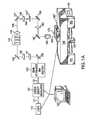
- the exemplary systemincludes a beam source 110 (e.g., a Lambda Physik model LPX-315I XeCl pulsed excimer laser) emitting an irradiation beam (e.g., a laser beam), a controllable beam energy density modulator 120 for modifying the energy density of the laser beam, a MicroLas two plate variable attenuator 130 (e.g., a device by MicroLas), beam steering mirrors 140 , 143 , 147 , 160 and 162 , beam expanding and collimating lenses 141 and 142 , a beam homogenizer 144 , a condenser lens 145 , a field lens 148 , a projection mask 150 which may be mounted in a translating stage (not shown), an eye piece 161 , a controllable shutter 152 , a multi-element objective lens 163 for focusing a radiation beam pulse 164 onto the sample 170 having the semiconductor thin film to be processed mounted on a sample
- the sample translation stage 180is preferably controlled by the computing arrangement 100 to effectuate translations of the sample 170 in the planar X-Y directions, as well as in the Z direction.
- the computing arrangement 100controls the relative position of the sample 170 with respect to the irradiation beam pulse 164 .
- the repetition and the energy density of the irradiation beam pulse 164are also controlled by the computing arrangement 100 .
- the irradiation beam pulsecan be generated by another known source of short energy pulses suitable for at least partially melting (and possibly fully melting throughout their entire thickness) selected areas of the semiconductor (e.g., silicon) thin film of the sample 170 in the manner described herein below.
- Such known sourcecan be a pulsed solid state laser, a chopped continuous wave laser, a pulsed electron beam and a pulsed ion beam, etc.
- the radiation beam pulses generated by the beam source 110provide a beam intensity in the range of 10 mJ/cm 2 to 1 J/cm 2 , a pulse duration (FWHM) in the range of 10 to 300 nsec, and a pulse repetition rate in the range of 10 Hz to 300 Hz.
- the computing arrangement 100controls translations of the sample 170 via the sample stage 180 for carrying out the processing of the semiconductor thin film of the sample 170 according to the present invention
- the computing arrangement 100may also be adapted to control the translations of the mask 150 and/or the beam source 110 mounted in an appropriate mask/laser beam translation stage (not shown for the simplicity of the depiction) to shift the intensity pattern of the irradiation beam pulses 164 , with respect to the semiconductor thin film of the sample 170 , along a controlled beam path.
- Another possible way to shift the intensity pattern of the irradiation beam pulseis to have the computing arrangement 100 control abeam steering mirror.
- the mask 150can be used by the exemplary system of the present invention to well define the profile of the resulting masked beam pulse 164 , and to reduce the non-uniformity of the adjacent portions and edge regions of the portions of the semiconductor thin film when these portions are irradiated by such masked beam pulse 164 and then crystallized.
- a semiconductor thin film 175 of the sample 170can be directly situated on, e.g., a glass substrate 172 , and may be provided on one or more intermediate layers 177 there between.
- the semiconductor thin film 175can have a thickness between 100 ⁇ and 10,000 ⁇ (1 ⁇ m) so long as at least certain necessary areas thereof can be at least partially or completely melted throughout their thickness.
- the semiconductor thin film 175(e.g., an amorphous silicon thin film) can be composed of silicon, germanium, silicon germanium (SeGe), etc. all of which preferably have low levels of impurities. It is also possible to utilize other elements or semiconductor materials for the semiconductor thin film 175 .
- the intermediary layer 177which is situated immediately underneath the semiconductor thin film 175 , can be composed of silicon oxide (SiO 2 ), silicon nitride (Si 3 N 4 ), and/or mixtures of oxide, nitride or other materials that are suitable for promoting grain growth within the designated areas of the semiconductor thin film 175 of the sample 170 .
- the temperature of the glass substrate 172can be between room temperature and 800° C. Higher temperatures of the glass substrate 172 can be accomplished by preheating the substrate 172 which would effectively allow larger grains to be grown in the irradiated, re-solidified, and then crystallized areas of the semiconductor thin film 175 of the sample 170 due to the proximity of the glass substrate 172 to the thin film 175 .
- the semiconductor thin film 175can be irradiated by the beam pulse 164 which can be shaped using the mask 150 according to an exemplary embodiment of the present invention as shown in FIG. 2 .
- the exemplary mask 150is sized such that its cross-sectional area is preferably larger than that of the cross-sectional area of the beam pulse 164 . In this manner, the mask 150 can pattern the pulsed beam to have a shape and profile directed by one or more open or transparent regions of the mask 150 .
- the exemplary embodiment of the mask 150 shown in FIG. 2includes an open or transparent region 157 that has a substantially long and narrow shape. This shape is defined by an opaque or beam-blocking region 155 .
- the open or transparent region 157(which may have a length L and a width A) permit beam pulses to irradiate there-through to at least partially melt the areas of the semiconductor thin film 175 that they impinge.
- Each of the beam pulses shaped by the mask 175has a shape substantially corresponding to the shape of the open or transparent region 157 .
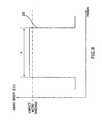
- FIG. 4Aillustrates a first exemplary profile of the beam pulse, along with particular dimensions of sections thereof, which can be shaped by the optics of the system illustrated in FIG. 1A and/or produced by the mask 150 of FIG. 2 .
- the shaped-beam pulse 200may have a particular width W′ (e.g., 300 ⁇ m to 1.2 mm) and a particular length L′ (e.g. 10 cm to 50 cm), both of which relating to the length L and the width W of the open/transparent region 157 of the mask 150 .
- the beam pulse 200thus produced by, e.g., the mask 150 extends for the length L to preferably process the entire length of the thin film sample 175 .
- the entire sample 170can be irradiated by the beam pulses 200 of the beam 164 as shown in FIG. 3 , and described in further detail below.
- the profile 220 of the beam pulse 200includes a top portion 205 , a leading edge portion 210 and a trailing edge portion 215 , all of which can extend for a particular distance.
- the top portion 205may extends for a distance A within which the energy density is at or above the complete melting threshold. This distance A can be between 200 ⁇ m to 1 mm.
- the leading edge portion 210can extend for a distance B 1 (e.g., between 50 ⁇ m and 100 ⁇ m), and the trailing edge portion 215 may extend for a distance B 2 (e.g., also between 50 ⁇ m and 100 ⁇ m).
- the leading edge potion 210has a section with a length of B 1 P, which extends from the point of the crystallization threshold to the point of the complete melting threshold, and which can be approximately half the size of the length B 1 .
- the trailing edge potion 215has a section with a length of B 2 P which extends from the point of the crystallization threshold to the point of the complete melting threshold, and which can be approximately half the size of the length B 2 .
- FIG. 4CA second exemplary profile of the beam pulse 200 is illustrated in FIG. 4C , which can also be shaped by the optics of the system illustrated in FIG. 1A and/or produced by the mask 150 of FIG. 2 .
- the energy density of the beam pulse 200has a profile 220 ′ with an energy density that is below the complete melting threshold.
- this profile 220 ′includes a top portion 205 ′, a leading edge portion 210 ′ and a trailing edge portion 215 ′.
- the top portion 205 ′ of this embodimentextends for a distance C, within which the energy density is approximately constant.
- the distance Cmay be between 200 ⁇ m to 1 mm.
- the leading edge portion 210 ′can extend for a distance D 1 (e.g., between 501 ⁇ m and 100 ⁇ m), and the trailing edge portion 215 ′ may extend for a distance D 2 (e.g., also between 50 ⁇ m and 100 ⁇ m).
- the leading edge potion 210 ′has a section with a length of DIP, which extends from to the point when the energy density is approximately constant to a lower point of the crystallization threshold.
- the trailing edge potion 215 ′has a section with a length of D 2 P which extends from the point of the crystallization threshold to a higher point of when the energy density is approximately constant.
- the pulses 200 of the line-type beam 164irradiate all rows of the thin film 175 provided on the semiconductor sample 170 in a controlled manner.
- the computing arrangement 100controls the beam source 110 to emit an initial beam so that the beam 164 (either masked by the mask 150 or shaped by the optics of the system) irradiates each row of the semiconductor thin film 175 provided on the sample 170 by translating the stage 180 on which the sample 170 is situated based on the location of the rows of the sample 170 , i.e., relative to the direction of the line-type beam 164 .
- the computing arrangement 100has a memory arrangement (not shown) which has stored thereon the location of each of the rows of the semiconductor thin film 175 which are to be irradiated by the beam pulse 200 . Therefore, the relative motion of the sample 170 with respect to the line-type beam 164 and the actuation of the beam source 110 are performed based on the locations of these rows. Such irradiation of the semiconductor thin film 175 by the line-type beam 164 is continued until all rows of the semiconductor thin film 175 provided on the sample 170 are irradiated by the line-type beam pulses 200 so that they re-solidify and form uniform-grained material areas.
- At least the areas in the rows of the semiconductor thin film 175 which are intended to situate microstructures (e.g., TFTs) thereonare preferably irradiated with the top portion 205 of the pulse 200 and fully melted so that these areas (e.g., pixels) can preferably be irradiated once by the convex top portion 205 of the pulse 200 shown in FIG. 4A . It is also possible to irradiate the semiconductor thin film 175 using the top portion 205 ′ of the pulse 200 illustrated in FIG. 4C . In this exemplary embodiment, the top portion 205 ′ has the energy density that is below the complete melting threshold of the thin film 175 , thereby only partially melting the thin film 175 .
- TFTsmicrostructures
- sections of the leading and trailing portions 210 , 215 of the embodiment of FIG. 4A and the portion 210 ′, 215 ′ of the embodiment shown in FIG. 4Ccan also irradiate the semiconductor thin film 175 in a similar manner, with certain limitations as shall be described in further detail below.
- FIG. 7illustrates sequential translations of the thin film 175 of the sample 170 with respect to the pulses 200 of the line-type beam 164 shaped by the optics of the system of FIG. 1A and/or patterned by the mask of FIG. 2 according to an exemplary embodiment of the present invention.
- the sample 170is translated in a ⁇ Y direction with respect to the direction of the line-type beam 164 .
- the beam source 110is actuated by the computing arrangement 100 so that a first line-type beam pulse 410 irradiates and at least partially melts, using a beam pulse 200 as depicted in FIG. 4C , or preferably fully melts, using a beam pulse 200 as described in FIG. 4A , one or more portions 511 - 519 at the first row 510 of the semiconductor thin film 175 .
- the profile and length of the first line-type pulse 410 shown in FIG. 7substantially corresponds to the profile and length of the pulse 200 illustrated in FIG. 4A .
- the width A of the convex top portion 205 of the first pulse 410is wide enough to irradiate and completely melt the entire cross-sections of the portions 511 - 519 .
- These portionscan be designated to place certain structures (e.g., TFTs) therein so that they can be used to define the pixels.
- TFTse.g., TFTs
- the resolidified portions which are partially meltedwould likely possess smaller crystallized-grain regions, but include uniform material therein.
- the line-type beam 164may have enough energy density to fully melt (throughout its thickness) the entire row 510 of the thin film 175 , or at least the portions 511 - 519 thereof using the top portion 205 of the profile 220 of the embodiment shown in FIG. 4A .
- Such fully melted and re-solidified portions of the thin film 175would have crystal-grains provided therein, which generally do not depend on the sensitivity of the fluence of the line-type beam 164 . In this manner, the negative effects of the energy density fluctuations of the of the line-type beam 164 on the uniformity of the resulting TFT devices provided in such re-solidified areas are minimized.
- the sample 170is translated in the ⁇ Y direction (via a control of the computing arrangement 100 ) so that the beam 164 impinges on a second row 520 of the semiconductor thin film 175 provided on the sample 170 .
- the beam source 110is actuated by the computing arrangement 100 to generate a second line-type pulse 420 which irradiates and either at least partially or fully melts one or more sections 521 - 529 of the second row 520 in substantially the same manner as described above with respect to the irradiation of the first row 510 .
- This translation of the sample 170(so that the impingement of the line-type beam 164 moves from the first row 510 to the second row 520 of the semiconductor thin film 175 ) is executed for a distance D.
- the distance Dcan be also referred to a pixel row periodicity since the translation of the sample 170 via the distance D is performed for other rows of the sample 170 .
- this distance Dis preferable for this distance D to be pre-assigned such that the trailing portion 215 ′ of the second line-type pulse 520 does not overlap the leading portion 210 ′ of the first line-type pulse 510 .
- the distance Dcan be measured from a center of the top portion 205 ′ of the first pulse 410 to a center of the top portion 205 ′ of the second pulse 420 . It is possible, however, to have certain sections of the trailing portion 215 ′ of the second line-type pulse 520 and of the leading portion 210 of the first line-type pulse 510 overlap one another. Such portions would preferably possess only the energy densities that are smaller than the crystallization threshold value.
- no portion of the subsequent pulse 200 of the profile 220 ′should overlap the section of the thin film 175 irradiated by the top portion 205 ′ of the preceding pulse 200 of such profile for the exemplary embodiment of FIG. 4C . This is because the flat top portion 205 ′ partially melts the thin film 175 , and generates grains of uniform size in such irradiated areas.
- any subsequent irradiation on this irradiated sectiontakes place, uniformity of this area may be compromised.
- the beam pulse 200 having the profile 220 of FIG. 4Ais utilized, then similar translation distance considerations exist, except that none of the portions of the profile 220 of the subsequent beam pulse 200 should overlap the section of the film sample 175 that was irradiated by the top portion 205 of the previous beam pulse 200 .
- the energy density of the top portion 205is above the complete melting threshold, and thus no portion of the subsequent beam pulse should overlap the completely melted previously section of the thin film 175 so as to avoid non-uniformity of such overlapped section due to the reirradiation thereof.
- the sample 170can then again be translated for the distance D in the same manner as described above with respect to the translation of the sample 164 so as to irradiate the second row 520 of the semiconductor thin film 175 .
- the line-type beam 164impinges the third row of the thin film 175 , and irradiates and partially melts one or more portions thereof.
- the width B 2 of the leading portion 210 (or width B 2 P) plus the width B 1 of the trailing portion 215 (or width B 1 P)should be smaller than the distance D.
- the leading portion 210 of the second line-type pulse 410 and the trailing portion 215 of the second line-type pulse 420would not overlap.
- the width D 2 of the leading portion 210 ′ (or width D 2 P) and the width D 1 of the trailing portion 215 ′ (or width D 1 P)should both be smaller than the distance D.
- the translation of the sample 170 with respect to the impingement thereof by the beam 164is performed continuously (e.g., without stopping).
- the computing arrangement 100can control the beam source 110 to generate the corresponding pulses 200 based on a predefined frequency.
- V of the continuous translation of the sample 170 with respect to the impingement of the semiconductor thin film 175by the line-type pulses 410 , 420 , so that the respective rows 510 , 520 of the thin film 175 are accurately irradiated by the pulses.
- the velocity Vcan be approximately 6 cm/sec, which can be a constant velocity.
- the actuation of the beam source 110can be controlled based on a positional signal provided by the translation stage 180 .
- This signalmay indicate the position of the sample 170 relative to the position of the impingement thereof by the line-type beam 164 .
- the computing arrangement 100can direct the actuation of the beam source 110 and the translation to the sample 170 to achieve an effective irradiation of specific portions (e.g., rows) of the semiconductor thin film 170 .
- the location controlled irradiation of at least portions of the semiconductor thin film 175can be achieved using a line-type beam 164 .
- the description above for the line-type beam 164has been directed to a Gaussian-shaped beam pulse, the examples of which is illustrated in FIGS. 4A and 4C .
- a top-hat line-type beam 250the exemplary profile of which is illustrated in FIG. 8 .
- this line-type beam 250has the energy density, which is greater than the complete melting threshold of the semiconductor thin film 175 . It should be understood that the energy density of this beam 250 can also be greater than or equal to the crystallization threshold of the semiconductor thin film 175 or above the complete melting threshold. As shown in FIG.
- the top hat line-type beam 250generally does not have any leading or trailing portions, and thus the distance D of the translation of the sample 170 does not have to be as great as would be preferable for the Gaussian-type beam.
- the top-hat line-type beam 250can be generated using a mask that has a knife edge aperture such that the beam source 110 provides a laser beam, which is then shaped by such a mask.
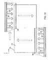
- FIG. 9Ashows an illustration of exemplary first and second irradiated, re-solidified and crystallized portions 511 and 512 of the first row 510 of the semiconductor thin film 175 illustrated in FIG. 7 .
- FIG. 9Ashows that the entire TFT devices 610 , 620 can be situated within the respective first and second portions 511 , 512 of the first row 510 .
- the first TFT device 610 situated in the first portion 511 of the first row 510includes a gate 612 , a drain 614 , a source 616 and an active region 618 .
- the second TFT device 620includes a gate 622 , a drain 624 , a source 626 and an active region 628 .
- FIG. 9Bshows an another exemplary illustration of the first and second irradiated, re-solidified and crystallized portions 511 and 512 of the first row 510 of the semiconductor thin film 175 , with the respective TFT devices 610 ′, 620 ′ provided thereon.
- the respective TFT devices 610 ′, 620 ′are provided thereon.
- only respective active regions 618 ′, 628 ′ of the TFT devices 610 ′, 620 ′are provided within the respective first and second crystallized portions 511 , 512 , while other portions of the TFT devices 610 ′, 620 ′ are situated on the borders of the these portions 511 , 512 .
- the first TFT device 610 ′includes an active region 618 ′ which entirely situated in the first portion 511 of the first row 510 , while a gate 612 ′, a drain 614 ′ and a source 616 ′ of this TFT device 610 ′ overlap the borders of the first portion 511 .
- an active region 628 ′ thereofis entirely situated within the respective second portion 512 of the first row 510 , while a gate 622 ′, a drain 624 ′ and a source 626 ′ of the second TFT device 620 ′ are provided directly on the borders of such second portion 512 .
- any one of the gate 612 , 612 ′, 622 , 622 ′, drain 614 , 614 ′, 624 , 624 ′ and source 616 , 616 ′, 626 , 626 ′can be provided on the first and second areas 511 , 512 and the border regions thereof.
- FIG. 10shows another exemplary illustration of sequential movements of the sample 170 by the translation stage 180 with respect to the impingement of the pulses of the line-type beam shaped by the optics of the system of FIG. 1A or patterned by the mask of FIG. 2 .
- the relative translation of the sample 170 with respect to the impingement by the line-type pulses 410 , 420are substantially similar to the relative translation of the sample described above with reference to FIG. 3 .
- the length of the line-type beam 164 in this embodimentis approximately half the length L of the embodiment of the line-type beam 164 of FIG. 3 .
- the 10can be 15 cm, irradiating the sample 170 which has a width which is smaller than 30 cm. Accordingly, using such beam length, the entire sample 170 is irradiated in two passes. In particular, one half of the sample 170 is irradiated in the manner described above with reference to FIG. 7 by, e.g., irradiating such half section of the sample 170 while translating the sample 170 in the ⁇ Y direction.
- the sample 170is translated in the ⁇ X direction, and second half section of the sample 170 is irradiated while translating the sample 175 in the +Y direction.
- the entire sample 170can be irradiated by the line-type beam 164 in two passes. It is also within the scope of the present invention to use the line-type beams which have shorter lengths, so that a larger number of passes are performed to completely process the sample 170 .
- FIG. 11shows a flow diagram representing an exemplary processing procedure of the present invention under at least partial control of the computing/processing arrangement 100 of FIG. 1A using the exemplary techniques of the present invention provided in FIGS. 7 and 10 .
- the hardware components of the system of FIG. 1Asuch as the beam source 110 , the energy beam modulator 120 , and the beam attenuator and shutter 130 are first initialized at least in part by the computing arrangement 100 .
- the sample 170is loaded onto the sample translation stage 180 in step 1005 . It should be noted that such loading may be performed either manually or automatically using known sample loading apparatus under the control of the computing arrangement 100 .
- the sample translation stage 180is moved, preferably under the control of the computing arrangement 100 , to an initial position in step 1010 .
- step 1020the irradiation/laser beam 111 is stabilized at a predetermined pulse energy level, pulse duration and repetition rate.
- step 1024it is preferably determined whether each beam pulse 164 has sufficient energy to at least partially melt (and preferably fully melt) the irradiated portions of the semiconductor thin film 175 without overheating.
- step 1024is executed again to determine if the there is sufficient energy to at least partially melt the portions of the semiconductor thin film 175 .
- step 1027the sample 170 is positioned to point the pulse 410 of the line-type beam 164 to impinge the first row 510 of the semiconductor thin film 175 .
- step 1030the respective row of the semiconductor thin film 175 is irradiated and at least partially melted using a masked intensity pattern (e.g., using the mask 150 illustrated in FIG. 2 ). Thereafter, the irradiated row (and/or portions thereof) of the semiconductor thin film 175 are allowed to solidify and crystallize.
- a masked intensity patterne.g., using the mask 150 illustrated in FIG. 2
- step 1045it is determined whether there are any more rows of the sample 170 that is to be subjected to the irradiation, i.e., whether the irradiation, melting and resolidification of the semiconductor thin film 175 has been completed. If not, in step 1050 , the sample 175 is translated so that the line-type beam impinges the next row of the sample 170 , and the processing is returned to step 1030 for irradiating of the current row of the semiconductor thin film 175 . However, if in step 1045 , it is determined that the irradiation and crystallization of the sample 170 is completed, and the hardware components and the beam 111 of the system shown in FIG. 1A can be shut off, and the process is terminated in step 1055 .
- Crystallization RateBeam Length ⁇ Frequency of Laser ⁇ Pitch
Landscapes
- Engineering & Computer Science (AREA)
- Physics & Mathematics (AREA)
- Chemical & Material Sciences (AREA)
- Computer Hardware Design (AREA)
- Power Engineering (AREA)
- Condensed Matter Physics & Semiconductors (AREA)
- General Physics & Mathematics (AREA)
- Manufacturing & Machinery (AREA)
- Microelectronics & Electronic Packaging (AREA)
- Crystallography & Structural Chemistry (AREA)
- Optics & Photonics (AREA)
- Materials Engineering (AREA)
- Metallurgy (AREA)
- Organic Chemistry (AREA)
- General Engineering & Computer Science (AREA)
- High Energy & Nuclear Physics (AREA)
- Electromagnetism (AREA)
- Recrystallisation Techniques (AREA)
Abstract
Description
- The present invention relates to techniques for processing of films, and more particularly to location-controlled techniques for processing semiconductor films using a line-type beam so as to obtain a substantial uniformity of certain regions of the thin films in which microstructures (e.g., thin-film transistor “TFT” devices) can be situated.
- Semiconductor films, such as silicon films, are known to be used for providing pixels for liquid crystal display devices. Certain prior art systems utilize line-type beams which are shaped to have a particular line-shape. An exemplary illustration of the line-
type beam pulse 200, and a profile thereof are illustrated inFIG. 4A . In particular, theline beam pulse 200 may defined by a length L and width W′. The profile of the line-type beam pulse 200 illustrated inFIG. 4A has a convextop portion 205, a large section of which has sufficient energy density to be below a complete melting energy density threshold. This profile of the line-type beam pulse 200 also has a leadingportion 210 and atrailing portion 215. The leadingportion 210 has an energy density beginning from a low or negligible energy density level, continuing to reach a crystallization threshold, and ending below the complete melting energy density threshold so as to reach the convextop portion 205. Thetrailing edge portion 215 has an energy density starting from the edge of the convex top portion205 (which is at a sufficient energy below the complete melting energy density threshold), passing the crystallization threshold, and ending at the low or negligible energy density level. The length L of the line beam can be between 10 cm and 50 cm so as to irradiate a significant section of a thin film provided on a sample. The conventional system generally use line beam pulses to irradiate the same section of the sample over 10 times with the energy density which is somewhat below the complete melting threshold. In this manner, a more uniform film may be attained, but the processing of such film is extremely slow. Indeed, the systems which use such line-type beam 200 are currently not suitable for quick processing of samples. In addition, when the edge portions (i.e., the leading andtrailing edge portions 210,215) irradiate the corresponding sections of the thin film, non-uniformity may be created in these sections. - As shown in
FIG. 4B , other conventional systems attempt to overcome these problems associated with non-uniformity by continuously scanningdisplay areas sample 180, until the entire area is completely irradiated. As shown inFIG. 5 , this is generally performed by irradiating areas of the sample using successive pulses of the line-type beam 200, such that a significant portion of the area irradiated by afirst pulse 300 of thebeam 200 is subsequently irradiated by thenext pulse 310. It follows that a sizable portion of the area of the sample irradiated by thepulse 310 is reirradiated by thesubsequent pulse 320. Also, a large portion of the area irradiated by thepulse 320 is reirradiated by thenext pulse 330, and so on. The overlap of the areas irradiated by the adjacent pulses is provided such that the distance between the adjacent pulses is the width of the top portion of the pulse divided by between 10 and 100, and preferably divided by approximately 20. - It may be possible to reduce the non-uniformity of the irradiated sections of the thin film sample by maintaining the energy density of the line-
type beam pulse 200 to be above the complete melting threshold. In particular, as shown inFIGS. 6A and 6B , sections of a thin film sample irradiated at an energy density above thecomplete melting threshold 250 form small polycrystalline grains compared to sections of the thin film sample irradiated at an energy density below the complete melting threshold. Between these sections, there is a narrow region where grains are very large, due to near-complete melting of the film. In addition, when the energy density is below the crystallization threshold, the irradiated area is amorphous. - It is conceivable to reduce the non-uniformity of the irradiated sections of the thin film sample by maintaining the energy density of the line-
type beam pulse 200 to be below the complete melting threshold. In particular, as shown inFIGS. 6C and 6D , sections of a thin film sample irradiated withbeam pulses 200 at a constant energy density that is above the crystallization threshold and below thecomplete melting threshold 205′ have an approximately uniform grain size. - However, there are disadvantages to the use of these conventional methods. For example, when the irradiated areas of the thin film are required to be overlapped, the processing time of the entire sample is slow. This is because the sample is processed to ensure the reirradiation of significant parts of the previously irradiated areas of the thin film.
- One of the objects of the present invention is to provide an improved process and system which irradiate at least one thin film section of the substrate using a line-type beam pulses so as to at least partially melt these sections, and without the irradiated areas being re-irradiated by the following beam pulses. In this manner, the melted sections of the thin film sections resolidify to form substantially uniform crystallized regions therein. Due to the uniformity of these regions of the resolidified thin film sections, it is possible to place the TFT devices in such regions. Thus, the TFT devices situated in such manner would likely have at least similar performance with respect to one another. Another object of the present invention is to continuously translate and irradiate one or more sections of the thin film sample (e.g., without stopping) such that the above-described uniformity is achieved in an accelerated manner.
- In one exemplary embodiment of the present invention, a process and system for processing a semiconductor thin film sample, as well as at least one portion of the semiconductor thin film structure are provided. In particular, a beam generator can be controlled to emit successive irradiation beam pulses at a predetermined repetition rate. Each of the irradiation beam pulses can be shaped to define at least one line-type beam pulse, with the line-type beam pulses being provided for impinging the film sample. These line-type beam pulses can include at least one part which have an intensity sufficient to at least partially melt irradiated portions of the film sample. Thereafter, a first portion of the film sample is irradiated using a first one of the line-type beam pulses to at least partially melt the first portion, with the irradiated first portion being allowed to resolidify and crystallize. After the irradiation of the first portion of the film sample, a second portion of the film sample is irradiated using a second one of the line-type beam pulses to at least partially melt the second portion, with the irradiated second portion also being allowed to resolidify and crystallize. An emission of the second one of the line-type beam pulses may immediately follow an emission of the first one of the line-type beam pulses. A profile of each of the line-type beam pulses may includes a leading portion, a top portion and a trailing portion. For example, a section of the first portion impacted by the top portion of the first one of the line-type beam pulses may be prevented from being irradiated by trailing portion of the second one of the line-type beam pulses.
- In another exemplary embodiment of the present invention, the first portion of the film sample is irradiated by the top portion of the first one of the line-type beam pulses, wherein the second portion of the film sample is irradiated by the top portion of the second one of the line-type beam pulses. The top portion of each of the line-type beam pulses may have energy density which is above a complete melting threshold Each of the leading and trailing portions of the first one of the line-type beam pulses can irradiate a part of the first portion, and each of the leading and trailing portions of the second one of the line-type beam pulses can irradiate a part of the second portion. In addition, each of leading and trailing portions of the first and second ones of the line-type beam pulses may include first and second sections. Each of the first sections of the leading and trailing portions of the first and second ones of the line-type beam pulses may include an energy density which is sufficient to at least partially melt the respective first portion and/or the respective second portion. Also, each of the second sections of the leading and trailing portions of the first and second ones of the line-type beam pulses can have an energy density lower than a threshold level which is sufficient to at least partially melt the part of one of the respective first portion and the respective second portion. The second portion can be irradiated after the irradiation of the first portion and after the film sample is translated for a particular distance with respect to an impingement by the beam pulses of the first portion. The first section of the leading portion of the first one of the line-type beam pulses may have a first length, and the first section of the trailing portion of the second one of the line-type beam pulses can have a second length. The top portion may have a third length. The particular distance can be greater than the sum of the third length and of the larger one of the first and second lengths.
- According to still another embodiment of the present invention, data associated with locations on the film sample to be irradiated is received. Then, after the irradiation of the first portion and before the irradiation of the second portion, the film sample is translated for a particular distance with respect to an impingement by the beam pulses based on such received data. The irradiation beam pulses can be shaped by a mask to define the line-type beam pulses. In addition, the first and second ones of the line-type beam pulses can at least partially melt the respective first and second portions of the film sample. Furthermore, the film sample can be translated for the particular distance with respect to an impingement by the beam pulses in a periodic manner and also based on an irradiation frequency of the irradiation beam generator. Also, the first and second portions of the film sample can include pixel areas. In addition, the first and second portions can include areas, which are configured to situate thereon an active region of at least one thin-film transistor “TFT” device.
- The accompanying drawings, which are incorporated and constitute part of this disclosure, illustrate a preferred embodiment of the invention and serve to explain the principles of the invention.
FIG. 1A is a schematic block diagram of an exemplary embodiment of an irradiation system according to the present invention which allows selected areas of a semiconductor thin film to be continuously scanned, at least partially melted and without re-irradiating these areas, in a predetermined controlled manner using a line-type beam;FIG. 1B is an enlarged cross-sectional side view of the sample which includes the semiconductor thin film;FIG. 2 is a top view of an exemplary embodiment of a mask according to the present invention utilized by the system illustratedFIG. 1A , which patterns a beam so as to have a line-type shape for irradiating the selected areas of the semiconductor thin film;FIG. 3 is an exemplary illustration of a continuous-motion irradiation of the entire semiconductor thin film using the system ofFIG. 1A and the mask ofFIG. 2 ;FIG. 4A is a cross-sectional profile of the line-type beam which can be shaped by optics of the system ofFIG. 1A and/or patterned by the mask ofFIG. 2 , and may be used for irradiating the semiconductor thin film according to a first exemplary embodiment of the present invention which has energy density above the complete melting threshold;FIG. 4B is an illustration of a continuous scan processing of the semiconductor thin film using conventional systems, which re-irradiate previously irradiated areas or apply beams whose energy density is below a complete melting threshold;FIG. 4C is a cross-sectional profile of the line-type beam according to a second exemplary embodiment of the present invention which has energy density above the crystallization threshold and below the complete melting threshold;FIG. 5 is an illustration of profiles of multiple line-type beams which re-irradiate previously irradiated portions of the semiconductor thin film;FIGS. 6A and 6B are examples of the results of irradiations of the conventional systems and methods when utilizing line-type beams whose energy densities are above the complete melting threshold;FIGS. 6C and 6D are examples of the results of irradiations of the conventional systems and methods when utilizing line-type beams whose energy densities are between the crystallization threshold and the complete melting threshold;FIG. 7 is an exemplary illustration of sequential movements of the semiconductor film of a sample with respect to the pulses of the line-type beam shaped by the optics of the system ofFIG. 1A or patterned by the mask ofFIG. 2 according to an exemplary embodiment of the present invention;FIG. 8 is a cross-sectional profile of another exemplary line-type beam which can be shaped by optics of the system ofFIG. 1A and/or patterned by the mask ofFIG. 2 , and which has either minimal or insignificant sloping edge portions;FIG. 9A is an illustration of the two particular areas irradiated, re-solidified and crystallized areas corresponding to the areas ofFIG. 7 in which the entire TFT device is situated on the small uniformed grained region formed through complete melting and re-solidification according to the present invention;FIG. 9B is an illustration of the two particular areas irradiated, re-solidified and crystallized areas corresponding to the areas ofFIG. 7 in which only the entire cross-section of the active region of the TFT device is situated in the small uniformed grained region formed through nucleation, while other regions are provided over border areas between the crystallized areas;FIG. 10 is another exemplary illustration of sequential movements of the semiconductor film of the sample with respect to the pulses of the line-type beam shaped by the optics of the system ofFIG. 1A or patterned by the mask ofFIG. 2 according to another exemplary embodiment of the present invention, in which the entire sample is irradiated in two passes; andFIG. 11 is a flow diagram representing an exemplary processing procedure of the present invention under at least partial control of a computing arrangement ofFIG. 1A using the exemplary techniques of the present invention ofFIGS. 7 and 10 .- It should be understood that various systems and methods according to the present invention can be utilized to at least partially melt, then solidify and crystallize one or more areas on a semiconductor thin film (e.g., silicon) using line-type beam pulses, while continuously translating the sample and without re-irradiating the previously irradiated and resolidified areas to generate substantially uniform regions on the thin film. The exemplary embodiments of the systems and process to generate such areas, as well as of the resulting crystallized semiconductor thin films shall be described in further detail below. However, it should be understood that the present invention is in no way limited to the exemplary embodiments of the systems, processes and semiconductor thin films described herein.
- Certain systems for providing a continuous motion SLS are described in U.S. patent application Ser. No. 09/526,585 (the “'585 application”), the entire disclosure of which is incorporated herein by reference. Substantially similar systems according to the exemplary embodiment of the present invention can be employed to generate at least partially irradiated, solidified and crystallized portions of the semiconductor film described above in which it is possible to process the entire semiconductor thin film in a controlled and accelerated manner with a line-type beam. In particular, the system according to the present invention can be used on a
sample 170 which has an amorphous thin film (e.g., silicon) thereon that is irradiated by irradiation beam pulses to promote the melting, subsequent solidification and crystallization of the particular areas of the semiconductor thin film. As shown inFIG. 1A , the exemplary system includes a beam source110 (e.g., a Lambda Physik model LPX-315I XeCl pulsed excimer laser) emitting an irradiation beam (e.g., a laser beam), a controllable beamenergy density modulator 120 for modifying the energy density of the laser beam, a MicroLas two plate variable attenuator130 (e.g., a device by MicroLas), beam steering mirrors140,143,147,160 and162, beam expanding andcollimating lenses beam homogenizer 144, acondenser lens 145, afield lens 148, aprojection mask 150 which may be mounted in a translating stage (not shown), aneye piece 161, a controllable shutter152, a multi-elementobjective lens 163 for focusing aradiation beam pulse 164 onto thesample 170 having the semiconductor thin film to be processed mounted on asample translation stage 180, a granite blockoptical bench 190 supported on a vibration isolation and self-levelingsystem beam source 110, the beamenergy density modulator 120, thevariable attenuator 130, the shutter152 and thesample translation stage 180. - The
sample translation stage 180 is preferably controlled by thecomputing arrangement 100 to effectuate translations of thesample 170 in the planar X-Y directions, as well as in the Z direction. In this manner, thecomputing arrangement 100 controls the relative position of thesample 170 with respect to theirradiation beam pulse 164. The repetition and the energy density of theirradiation beam pulse 164 are also controlled by thecomputing arrangement 100. It should be understood by those skilled in the art that instead of the beam source110 (e.g., the pulsed excimer laser), the irradiation beam pulse can be generated by another known source of short energy pulses suitable for at least partially melting (and possibly fully melting throughout their entire thickness) selected areas of the semiconductor (e.g., silicon) thin film of thesample 170 in the manner described herein below. Such known source can be a pulsed solid state laser, a chopped continuous wave laser, a pulsed electron beam and a pulsed ion beam, etc. Typically, the radiation beam pulses generated by thebeam source 110 provide a beam intensity in the range of 10 mJ/cm2to 1 J/cm2, a pulse duration (FWHM) in the range of 10 to 300 nsec, and a pulse repetition rate in the range of 10 Hz to 300 Hz. - While the
computing arrangement 100, in the exemplary embodiment of the system shown inFIG. 1A , controls translations of thesample 170 via thesample stage 180 for carrying out the processing of the semiconductor thin film of thesample 170 according to the present invention, thecomputing arrangement 100 may also be adapted to control the translations of themask 150 and/or thebeam source 110 mounted in an appropriate mask/laser beam translation stage (not shown for the simplicity of the depiction) to shift the intensity pattern of theirradiation beam pulses 164, with respect to the semiconductor thin film of thesample 170, along a controlled beam path. Another possible way to shift the intensity pattern of the irradiation beam pulse is to have thecomputing arrangement 100 control abeam steering mirror. The exemplary system ofFIG. 1A may be used to carry out the processing of the semiconductor thin film of thesample 170 in the manner described below in further detail. Themask 150 can be used by the exemplary system of the present invention to well define the profile of the resultingmasked beam pulse 164, and to reduce the non-uniformity of the adjacent portions and edge regions of the portions of the semiconductor thin film when these portions are irradiated by suchmasked beam pulse 164 and then crystallized. - As illustrated in
FIG. 1B , a semiconductorthin film 175 of thesample 170 can be directly situated on, e.g., aglass substrate 172, and may be provided on one or moreintermediate layers 177 there between. The semiconductorthin film 175 can have a thickness between 100 Å and 10,000 Å (1 μm) so long as at least certain necessary areas thereof can be at least partially or completely melted throughout their thickness. - According to an exemplary embodiment of the present invention, the semiconductor thin film175 (e.g., an amorphous silicon thin film) can be composed of silicon, germanium, silicon germanium (SeGe), etc. all of which preferably have low levels of impurities. It is also possible to utilize other elements or semiconductor materials for the semiconductor
thin film 175. Theintermediary layer 177, which is situated immediately underneath the semiconductorthin film 175, can be composed of silicon oxide (SiO2), silicon nitride (Si3N4), and/or mixtures of oxide, nitride or other materials that are suitable for promoting grain growth within the designated areas of the semiconductorthin film 175 of thesample 170. The temperature of theglass substrate 172 can be between room temperature and 800° C. Higher temperatures of theglass substrate 172 can be accomplished by preheating thesubstrate 172 which would effectively allow larger grains to be grown in the irradiated, re-solidified, and then crystallized areas of the semiconductorthin film 175 of thesample 170 due to the proximity of theglass substrate 172 to thethin film 175. - The semiconductor
thin film 175 can be irradiated by thebeam pulse 164 which can be shaped using themask 150 according to an exemplary embodiment of the present invention as shown inFIG. 2 . Theexemplary mask 150 is sized such that its cross-sectional area is preferably larger than that of the cross-sectional area of thebeam pulse 164. In this manner, themask 150 can pattern the pulsed beam to have a shape and profile directed by one or more open or transparent regions of themask 150. The exemplary embodiment of themask 150 shown inFIG. 2 includes an open ortransparent region 157 that has a substantially long and narrow shape. This shape is defined by an opaque or beam-blockingregion 155. The open or transparent region157 (which may have a length L and a width A) permit beam pulses to irradiate there-through to at least partially melt the areas of the semiconductorthin film 175 that they impinge. Each of the beam pulses shaped by themask 175 has a shape substantially corresponding to the shape of the open ortransparent region 157. - An example of
such beam pulse 200 is shown inFIG. 4A , which illustrates a first exemplary profile of the beam pulse, along with particular dimensions of sections thereof, which can be shaped by the optics of the system illustrated inFIG. 1A and/or produced by themask 150 ofFIG. 2 . In particular, the shaped-beam pulse 200 may have a particular width W′ (e.g., 300 μm to 1.2 mm) and a particular length L′ (e.g. 10 cm to 50 cm), both of which relating to the length L and the width W of the open/transparent region 157 of themask 150. In this manner, thebeam pulse 200 thus produced by, e.g., themask 150 extends for the length L to preferably process the entire length of thethin film sample 175. Theentire sample 170 can be irradiated by thebeam pulses 200 of thebeam 164 as shown inFIG. 3 , and described in further detail below. Theprofile 220 of thebeam pulse 200 includes atop portion 205, aleading edge portion 210 and a trailingedge portion 215, all of which can extend for a particular distance. Thetop portion 205 may extends for a distance A within which the energy density is at or above the complete melting threshold. This distance A can be between 200 μm to 1 mm. Theleading edge portion 210 can extend for a distance B1 (e.g., between 50 μm and 100 μm), and the trailingedge portion 215 may extend for a distance B2 (e.g., also between 50 μm and 100 μm). Theleading edge potion 210 has a section with a length of B1P, which extends from the point of the crystallization threshold to the point of the complete melting threshold, and which can be approximately half the size of the length B1. Similarly, the trailingedge potion 215 has a section with a length of B2P which extends from the point of the crystallization threshold to the point of the complete melting threshold, and which can be approximately half the size of the length B2. - A second exemplary profile of the
beam pulse 200 is illustrated inFIG. 4C , which can also be shaped by the optics of the system illustrated inFIG. 1A and/or produced by themask 150 ofFIG. 2 . In this second exemplary embodiment, the energy density of thebeam pulse 200 has aprofile 220′ with an energy density that is below the complete melting threshold. In particular, thisprofile 220′ includes atop portion 205′, aleading edge portion 210′ and a trailingedge portion 215′. Thetop portion 205′ of this embodiment extends for a distance C, within which the energy density is approximately constant. The distance C may be between 200 μm to 1 mm. Theleading edge portion 210′ can extend for a distance D1 (e.g., between 501 μm and 100 μm), and the trailingedge portion 215′ may extend for a distance D2 (e.g., also between 50 μm and 100 μm). Theleading edge potion 210′ has a section with a length of DIP, which extends from to the point when the energy density is approximately constant to a lower point of the crystallization threshold. Similarly, the trailingedge potion 215′ has a section with a length of D2P which extends from the point of the crystallization threshold to a higher point of when the energy density is approximately constant. - As shown in
FIG. 3 , according to an exemplary embodiment of the present invention, thepulses 200 of the line-type beam 164 irradiate all rows of thethin film 175 provided on thesemiconductor sample 170 in a controlled manner. For example, thecomputing arrangement 100 controls thebeam source 110 to emit an initial beam so that the beam164 (either masked by themask 150 or shaped by the optics of the system) irradiates each row of the semiconductorthin film 175 provided on thesample 170 by translating thestage 180 on which thesample 170 is situated based on the location of the rows of thesample 170, i.e., relative to the direction of the line-type beam 164. In particular, thecomputing arrangement 100 has a memory arrangement (not shown) which has stored thereon the location of each of the rows of the semiconductorthin film 175 which are to be irradiated by thebeam pulse 200. Therefore, the relative motion of thesample 170 with respect to the line-type beam 164 and the actuation of thebeam source 110 are performed based on the locations of these rows. Such irradiation of the semiconductorthin film 175 by the line-type beam 164 is continued until all rows of the semiconductorthin film 175 provided on thesample 170 are irradiated by the line-type beam pulses 200 so that they re-solidify and form uniform-grained material areas. According to a preferred embodiment of the present invention, at least the areas in the rows of the semiconductorthin film 175 which are intended to situate microstructures (e.g., TFTs) thereon are preferably irradiated with thetop portion 205 of thepulse 200 and fully melted so that these areas (e.g., pixels) can preferably be irradiated once by the convextop portion 205 of thepulse 200 shown inFIG. 4A . It is also possible to irradiate the semiconductorthin film 175 using thetop portion 205′ of thepulse 200 illustrated inFIG. 4C . In this exemplary embodiment, thetop portion 205′ has the energy density that is below the complete melting threshold of thethin film 175, thereby only partially melting thethin film 175. Of course, sections of the leading and trailingportions FIG. 4A and theportion 210′,215′ of the embodiment shown inFIG. 4C can also irradiate the semiconductorthin film 175 in a similar manner, with certain limitations as shall be described in further detail below. FIG. 7 illustrates sequential translations of thethin film 175 of thesample 170 with respect to thepulses 200 of the line-type beam 164 shaped by the optics of the system ofFIG. 1A and/or patterned by the mask ofFIG. 2 according to an exemplary embodiment of the present invention. In this exemplary illustration of the irradiation of the semiconductorthin film 175 provided on thesample 170, thesample 170 is translated in a −Y direction with respect to the direction of the line-type beam 164. When thesample 170 is translated in this manner to a position such that the line-type beam 164 points at afirst row 510 of thethin film 175, thebeam source 110 is actuated by thecomputing arrangement 100 so that a first line-type beam pulse 410 irradiates and at least partially melts, using abeam pulse 200 as depicted inFIG. 4C , or preferably fully melts, using abeam pulse 200 as described inFIG. 4A , one or more portions511-519 at thefirst row 510 of the semiconductorthin film 175. The profile and length of the first line-type pulse 410 shown inFIG. 7 substantially corresponds to the profile and length of thepulse 200 illustrated inFIG. 4A . It is preferable for the width A of the convextop portion 205 of thefirst pulse 410 to be wide enough to irradiate and completely melt the entire cross-sections of the portions511-519. These portions can be designated to place certain structures (e.g., TFTs) therein so that they can be used to define the pixels. The resolidified portions which are partially melted would likely possess smaller crystallized-grain regions, but include uniform material therein.- Upon the irradiation and at least partial melting of such portions511-519 using the
top portion 205 of theprofile 220′ of the embodiment shown inFIG. 4C in thefirst row 510 of the semiconductorthin film 175 as described above, the melted portions511-519 resolidify and crystallize so that they have uniform crystal grain growth therein. According to another exemplary embodiment of the present invention and also as mentioned above, the line-type beam 164 may have enough energy density to fully melt (throughout its thickness) theentire row 510 of thethin film 175, or at least the portions511-519 thereof using thetop portion 205 of theprofile 220 of the embodiment shown inFIG. 4A . Such fully melted and re-solidified portions of thethin film 175 would have crystal-grains provided therein, which generally do not depend on the sensitivity of the fluence of the line-type beam 164. In this manner, the negative effects of the energy density fluctuations of the of the line-type beam 164 on the uniformity of the resulting TFT devices provided in such re-solidified areas are minimized. - After the
first row 510 is irradiated and either partially or fully melted using the line-type pulse 410 as described above, thesample 170 is translated in the −Y direction (via a control of the computing arrangement100) so that thebeam 164 impinges on asecond row 520 of the semiconductorthin film 175 provided on thesample 170. As for thefirst row 510 and upon reaching thesecond row 520, thebeam source 110 is actuated by thecomputing arrangement 100 to generate a second line-type pulse 420 which irradiates and either at least partially or fully melts one or more sections521-529 of thesecond row 520 in substantially the same manner as described above with respect to the irradiation of thefirst row 510. This translation of the sample170 (so that the impingement of the line-type beam 164 moves from thefirst row 510 to thesecond row 520 of the semiconductor thin film175) is executed for a distance D. The distance D can be also referred to a pixel row periodicity since the translation of thesample 170 via the distance D is performed for other rows of thesample 170. - It is preferable for this distance D to be pre-assigned such that the trailing
portion 215′ of the second line-type pulse 520 does not overlap the leadingportion 210′ of the first line-type pulse 510. For example, the distance D can be measured from a center of thetop portion 205′ of thefirst pulse 410 to a center of thetop portion 205′ of thesecond pulse 420. It is possible, however, to have certain sections of the trailingportion 215′ of the second line-type pulse 520 and of the leadingportion 210 of the first line-type pulse 510 overlap one another. Such portions would preferably possess only the energy densities that are smaller than the crystallization threshold value. Thus, preferably, no portion of thesubsequent pulse 200 of theprofile 220′ should overlap the section of thethin film 175 irradiated by thetop portion 205′ of the precedingpulse 200 of such profile for the exemplary embodiment ofFIG. 4C . This is because the flattop portion 205′ partially melts thethin film 175, and generates grains of uniform size in such irradiated areas. - If any subsequent irradiation on this irradiated section takes place, uniformity of this area may be compromised. Similarly, if the
beam pulse 200 having theprofile 220 ofFIG. 4A is utilized, then similar translation distance considerations exist, except that none of the portions of theprofile 220 of thesubsequent beam pulse 200 should overlap the section of thefilm sample 175 that was irradiated by thetop portion 205 of theprevious beam pulse 200. However, contrary to the use of thebeam pulse 200 of the embodiment ofFIG. 4C , the energy density of thetop portion 205 is above the complete melting threshold, and thus no portion of the subsequent beam pulse should overlap the completely melted previously section of thethin film 175 so as to avoid non-uniformity of such overlapped section due to the reirradiation thereof. - The
sample 170 can then again be translated for the distance D in the same manner as described above with respect to the translation of thesample 164 so as to irradiate thesecond row 520 of the semiconductorthin film 175. Upon such translation, the line-type beam 164 impinges the third row of thethin film 175, and irradiates and partially melts one or more portions thereof. - Thus, for the embodiment of
FIG. 4A , the width B2 of the leading portion210 (or width B2P) plus the width B1 of the trailing portion215 (or width B1P) should be smaller than the distance D. In this manner, the leadingportion 210 of the second line-type pulse 410 and the trailingportion 215 of the second line-type pulse 420 would not overlap. For the embodiment ofFIG. 4C , in a similar manner, the width D2 of the leadingportion 210′ (or width D2P) and the width D1 of the trailingportion 215′ (or width D1P) should both be smaller than the distance D. - According to one exemplary embodiment of the present invention, the translation of the
sample 170 with respect to the impingement thereof by thebeam 164 is performed continuously (e.g., without stopping). Thecomputing arrangement 100 can control thebeam source 110 to generate the correspondingpulses 200 based on a predefined frequency. In this manner, it is possible to define the velocity V of the continuous translation of thesample 170 with respect to the impingement of the semiconductorthin film 175 by the line-type pulses respective rows thin film 175 are accurately irradiated by the pulses. For example, this velocity V of the translation of thesample 170 can be defined as follows:
V=D×flaser
where flaseris the frequency of the laser. Thus, if the distance D is 200 μm and the flaseris 300 Hz, the velocity V can be approximately 6 cm/sec, which can be a constant velocity. - According to another embodiment of the present invention, while the
sample 170 does not have to be continuously translated with respect to the impingement thereof by thebeam 164, the actuation of thebeam source 110 can be controlled based on a positional signal provided by thetranslation stage 180. This signal may indicate the position of thesample 170 relative to the position of the impingement thereof by the line-type beam 164. Based on the data associated with such signal, thecomputing arrangement 100 can direct the actuation of thebeam source 110 and the translation to thesample 170 to achieve an effective irradiation of specific portions (e.g., rows) of the semiconductorthin film 170. Thus, the location controlled irradiation of at least portions of the semiconductorthin film 175 can be achieved using a line-type beam 164. - The description above for the line-
type beam 164 has been directed to a Gaussian-shaped beam pulse, the examples of which is illustrated inFIGS. 4A and 4C . According to yet another exemplary embodiment of the present invention, it is also possible to utilize a top-hat line-type beam 250, the exemplary profile of which is illustrated inFIG. 8 . In particular, this line-type beam 250 has the energy density, which is greater than the complete melting threshold of the semiconductorthin film 175. It should be understood that the energy density of thisbeam 250 can also be greater than or equal to the crystallization threshold of the semiconductorthin film 175 or above the complete melting threshold. As shown inFIG. 8 , the top hat line-type beam 250 generally does not have any leading or trailing portions, and thus the distance D of the translation of thesample 170 does not have to be as great as would be preferable for the Gaussian-type beam. The top-hat line-type beam 250 can be generated using a mask that has a knife edge aperture such that thebeam source 110 provides a laser beam, which is then shaped by such a mask. FIG. 9A shows an illustration of exemplary first and second irradiated, re-solidified and crystallizedportions first row 510 of the semiconductorthin film 175 illustrated inFIG. 7 . In particular,FIG. 9A shows that theentire TFT devices second portions first row 510. Thefirst TFT device 610 situated in thefirst portion 511 of thefirst row 510 includes agate 612, adrain 614, asource 616 and anactive region 618. Similarly, thesecond TFT device 620 includes agate 622, adrain 624, asource 626 and anactive region 628.FIG. 9B shows an another exemplary illustration of the first and second irradiated, re-solidified and crystallizedportions first row 510 of the semiconductorthin film 175, with therespective TFT devices 610′,620′ provided thereon. In this exemplary embodiment, only respectiveactive regions 618′,628′ of theTFT devices 610′,620′ are provided within the respective first and secondcrystallized portions TFT devices 610′,620′ are situated on the borders of the theseportions first TFT device 610′ includes anactive region 618′ which entirely situated in thefirst portion 511 of thefirst row 510, while agate 612′, adrain 614′ and asource 616′ of thisTFT device 610′ overlap the borders of thefirst portion 511. Also, for thesecond TFT device 610′, anactive region 628′ thereof is entirely situated within the respectivesecond portion 512 of thefirst row 510, while agate 622′, adrain 624′ and asource 626′ of thesecond TFT device 620′ are provided directly on the borders of suchsecond portion 512. It should be understood that any one of thegate source second areas - It should be understood that the above description is equally applicable for all portions511-519,521-529, etc. of the semiconductor
thin film 175. In addition, the above placement of theactive regions FIG. 10 shows another exemplary illustration of sequential movements of thesample 170 by thetranslation stage 180 with respect to the impingement of the pulses of the line-type beam shaped by the optics of the system ofFIG. 1A or patterned by the mask ofFIG. 2 . In this exemplary embodiment, the relative translation of thesample 170 with respect to the impingement by the line-type pulses FIG. 3 . However, the length of the line-type beam 164 in this embodiment is approximately half the length L of the embodiment of the line-type beam 164 ofFIG. 3 . For example, the profile of the line-type beam 164 shown inFIG. 10 can be 15 cm, irradiating thesample 170 which has a width which is smaller than 30 cm. Accordingly, using such beam length, theentire sample 170 is irradiated in two passes. In particular, one half of thesample 170 is irradiated in the manner described above with reference toFIG. 7 by, e.g., irradiating such half section of thesample 170 while translating thesample 170 in the −Y direction. When the impingement of the line-type beam 164 completes the irradiation of the entire half section of the sample170 (i.e., reaches an opposite edge from which the irradiation began), thesample 170 is translated in the −X direction, and second half section of thesample 170 is irradiated while translating thesample 175 in the +Y direction. Thus, theentire sample 170 can be irradiated by the line-type beam 164 in two passes. It is also within the scope of the present invention to use the line-type beams which have shorter lengths, so that a larger number of passes are performed to completely process thesample 170.FIG. 11 shows a flow diagram representing an exemplary processing procedure of the present invention under at least partial control of the computing/processing arrangement 100 ofFIG. 1A using the exemplary techniques of the present invention provided inFIGS. 7 and 10 . Instep 1000, the hardware components of the system ofFIG. 1A , such as thebeam source 110, theenergy beam modulator 120, and the beam attenuator and shutter130 are first initialized at least in part by thecomputing arrangement 100. Thesample 170 is loaded onto thesample translation stage 180 instep 1005. It should be noted that such loading may be performed either manually or automatically using known sample loading apparatus under the control of thecomputing arrangement 100. Next, thesample translation stage 180 is moved, preferably under the control of thecomputing arrangement 100, to an initial position instep 1010.- Various other optical components of the system are adjusted and/or aligned either manually or under the control of the
computing arrangement 100 for a proper focus and alignment in step1015, if necessary. Instep 1020, the irradiation/laser beam 111 is stabilized at a predetermined pulse energy level, pulse duration and repetition rate. Instep 1024, it is preferably determined whether eachbeam pulse 164 has sufficient energy to at least partially melt (and preferably fully melt) the irradiated portions of the semiconductorthin film 175 without overheating. If that is not the case, the attenuation of thebeam 111 is adjusted by thebeams source 110 under the control of thecomputing arrangement 100 instep 1025, andstep 1024 is executed again to determine if the there is sufficient energy to at least partially melt the portions of the semiconductorthin film 175. - In
step 1027, thesample 170 is positioned to point thepulse 410 of the line-type beam 164 to impinge thefirst row 510 of the semiconductorthin film 175. Then, instep 1030, the respective row of the semiconductorthin film 175 is irradiated and at least partially melted using a masked intensity pattern (e.g., using themask 150 illustrated inFIG. 2 ). Thereafter, the irradiated row (and/or portions thereof) of the semiconductorthin film 175 are allowed to solidify and crystallize. Instep 1045, it is determined whether there are any more rows of thesample 170 that is to be subjected to the irradiation, i.e., whether the irradiation, melting and resolidification of the semiconductorthin film 175 has been completed. If not, instep 1050, thesample 175 is translated so that the line-type beam impinges the next row of thesample 170, and the processing is returned to step1030 for irradiating of the current row of the semiconductorthin film 175. However, if instep 1045, it is determined that the irradiation and crystallization of thesample 170 is completed, and the hardware components and thebeam 111 of the system shown inFIG. 1A can be shut off, and the process is terminated instep 1055. - Using the system and process according to the present invention, it is possible to obtain a significantly greater crystallization rate over that of the conventional systems and processes. This crystallization rate is provided as follows:
Crystallization Rate=Beam Length×Frequency of Laser×Pitch
For example, the crystallization rate effectuated by conventional system and process is:
50 cm×20 μm×300 Hz=30 cm2/sec (for a20 shot process)
In contrast, the crystallization rate afforded by the system and process according to the present invention is:
50 cm×300 μm×300 Hz=450 cm2/sec. - The foregoing merely illustrates the principles of the invention. Various modifications and alterations to the described embodiments will be apparent to those skilled in the art in view of the teachings herein. For example, while the above embodiment has been described with respect to at least partial or full solidification and crystallization of the semiconductor thin film, it may apply to other materials processing techniques, such as micro-machining, photo-ablation, and micro-patterning techniques, including those described in International patent application no. PCT/US01/12799 and U.S. patent application Ser. Nos. 09/390,535, 09/390,537 and 09/526,585, the entire disclosures of which are incorporated herein by reference. The various mask patterns and intensity beam patterns described in the above-referenced patent application can also be utilized with the process and system of the present invention so long as a line-type beam pulses are generated. It will thus be appreciated that those skilled in the art will be able to devise numerous systems and methods which, although not explicitly shown or described herein, embody the principles of the invention and are thus within the spirit and scope of the present invention.
Claims (41)
Priority Applications (2)
| Application Number | Priority Date | Filing Date | Title |
|---|---|---|---|
| US11/373,772US8796159B2 (en) | 2003-09-16 | 2006-03-09 | Processes and systems for laser crystallization processing of film regions on a substrate utilizing a line-type beam, and structures of such film regions |
| US14/311,570US9466402B2 (en) | 2003-09-16 | 2014-06-23 | Processes and systems for laser crystallization processing of film regions on a substrate utilizing a line-type beam, and structures of such film regions |
Applications Claiming Priority (3)
| Application Number | Priority Date | Filing Date | Title |
|---|---|---|---|
| US50336103P | 2003-09-16 | 2003-09-16 | |
| PCT/US2004/030330WO2005029551A2 (en) | 2003-09-16 | 2004-09-16 | Processes and systems for laser crystallization processing of film regions on a substrate utilizing a line-type beam, and structures of such film regions |
| US11/373,772US8796159B2 (en) | 2003-09-16 | 2006-03-09 | Processes and systems for laser crystallization processing of film regions on a substrate utilizing a line-type beam, and structures of such film regions |
Related Parent Applications (1)
| Application Number | Title | Priority Date | Filing Date |
|---|---|---|---|
| PCT/US2004/030330ContinuationWO2005029551A2 (en) | 2003-09-16 | 2004-09-16 | Processes and systems for laser crystallization processing of film regions on a substrate utilizing a line-type beam, and structures of such film regions |
Related Child Applications (1)
| Application Number | Title | Priority Date | Filing Date |
|---|---|---|---|
| US14/311,570DivisionUS9466402B2 (en) | 2003-09-16 | 2014-06-23 | Processes and systems for laser crystallization processing of film regions on a substrate utilizing a line-type beam, and structures of such film regions |
Publications (2)
| Publication Number | Publication Date |
|---|---|
| US20070010104A1true US20070010104A1 (en) | 2007-01-11 |
| US8796159B2 US8796159B2 (en) | 2014-08-05 |
Family
ID=34375343
Family Applications (2)
| Application Number | Title | Priority Date | Filing Date |
|---|---|---|---|
| US11/373,772Active2025-12-19US8796159B2 (en) | 2003-09-16 | 2006-03-09 | Processes and systems for laser crystallization processing of film regions on a substrate utilizing a line-type beam, and structures of such film regions |
| US14/311,570Expired - Fee RelatedUS9466402B2 (en) | 2003-09-16 | 2014-06-23 | Processes and systems for laser crystallization processing of film regions on a substrate utilizing a line-type beam, and structures of such film regions |
Family Applications After (1)
| Application Number | Title | Priority Date | Filing Date |
|---|---|---|---|
| US14/311,570Expired - Fee RelatedUS9466402B2 (en) | 2003-09-16 | 2014-06-23 | Processes and systems for laser crystallization processing of film regions on a substrate utilizing a line-type beam, and structures of such film regions |
Country Status (3)
| Country | Link |
|---|---|
| US (2) | US8796159B2 (en) |
| TW (1) | TWI359441B (en) |
| WO (1) | WO2005029551A2 (en) |
Cited By (33)
| Publication number | Priority date | Publication date | Assignee | Title |
|---|---|---|---|---|
| US20060040512A1 (en)* | 2002-08-19 | 2006-02-23 | Im James S | Single-shot semiconductor processing system and method having various irradiation patterns |
| US20060102901A1 (en)* | 2004-11-18 | 2006-05-18 | The Trustees Of Columbia University In The City Of New York | Systems and methods for creating crystallographic-orientation controlled poly-Silicon films |
| US20060254500A1 (en)* | 2005-04-06 | 2006-11-16 | The Trustees Of Columbia University In The City Of New York | Line scan sequential lateral solidification of thin films |
| US20070010074A1 (en)* | 2003-09-16 | 2007-01-11 | Im James S | Method and system for facilitating bi-directional growth |
| US20080176414A1 (en)* | 2003-09-16 | 2008-07-24 | Columbia University | Systems and methods for inducing crystallization of thin films using multiple optical paths |
| US20090001523A1 (en)* | 2005-12-05 | 2009-01-01 | Im James S | Systems and Methods for Processing a Film, and Thin Films |
| US20090045181A1 (en)* | 2003-09-16 | 2009-02-19 | The Trustees Of Columbia University In The City Of New York | Systems and methods for processing thin films |
| US20090130795A1 (en)* | 2007-11-21 | 2009-05-21 | Trustees Of Columbia University | Systems and methods for preparation of epitaxially textured thick films |
| US20090173948A1 (en)* | 1996-05-28 | 2009-07-09 | Im James S | Uniform large-grained and grain boundary location manipulated polycrystalline thin film semiconductors formed using sequential lateral solidification and devices formed thereon |
| US20090218577A1 (en)* | 2005-08-16 | 2009-09-03 | Im James S | High throughput crystallization of thin films |
| US20090242805A1 (en)* | 2005-08-16 | 2009-10-01 | Im James S | Systems and methods for uniform sequential lateral solidification of thin films using high frequency lasers |
| US20100065853A1 (en)* | 2002-08-19 | 2010-03-18 | Im James S | Process and system for laser crystallization processing of film regions on a substrate to minimize edge areas, and structure of such film regions |
| US20100187529A1 (en)* | 2003-09-16 | 2010-07-29 | Columbia University | Laser-irradiated thin films having variable thickness |
| US20110097907A1 (en)* | 2008-06-26 | 2011-04-28 | Ihi Corporation | Laser annealing method and apparatus |
| US20110101368A1 (en)* | 2008-02-29 | 2011-05-05 | The Trustees Of Columbia University In The City Of New York | Flash lamp annealing crystallization for large area thin films |
| US20110108843A1 (en)* | 2007-09-21 | 2011-05-12 | The Trustees Of Columbia University In The City Of New York | Collections of laterally crystallized semiconductor islands for use in thin film transistors |
| US20110108108A1 (en)* | 2008-02-29 | 2011-05-12 | The Trustees Of Columbia University In The City Of | Flash light annealing for thin films |
| US20110108535A1 (en)* | 2008-06-30 | 2011-05-12 | Ihi Corporation | Laser annealing apparatus |
| US20110121306A1 (en)* | 2009-11-24 | 2011-05-26 | The Trustees Of Columbia University In The City Of New York | Systems and Methods for Non-Periodic Pulse Sequential Lateral Solidification |
| US20110175099A1 (en)* | 2008-02-29 | 2011-07-21 | The Trustees Of Columbia University In The City Of New York | Lithographic method of making uniform crystalline si films |
| US8012861B2 (en) | 2007-11-21 | 2011-09-06 | The Trustees Of Columbia University In The City Of New York | Systems and methods for preparing epitaxially textured polycrystalline films |
| US20120273792A1 (en)* | 2010-01-20 | 2012-11-01 | Integrated Photovoltaic, Inc. | Zone Melt Recrystallization of Thin Films |
| US8415670B2 (en) | 2007-09-25 | 2013-04-09 | The Trustees Of Columbia University In The City Of New York | Methods of producing high uniformity in thin film transistor devices fabricated on laterally crystallized thin films |
| US8426296B2 (en) | 2007-11-21 | 2013-04-23 | The Trustees Of Columbia University In The City Of New York | Systems and methods for preparing epitaxially textured polycrystalline films |
| US8445365B2 (en) | 2003-09-19 | 2013-05-21 | The Trustees Of Columbia University In The City Of New York | Single scan irradiation for crystallization of thin films |
| US8476144B2 (en) | 2003-09-16 | 2013-07-02 | The Trustees Of Columbia University In The City Of New York | Method for providing a continuous motion sequential lateral solidification for reducing or eliminating artifacts in edge regions, and a mask for facilitating such artifact reduction/elimination |
| WO2013172965A1 (en)* | 2012-05-14 | 2013-11-21 | The Trustees Of Columbia University In The City Of New York | Advanced excimer laser annealing for thin films |
| US8796159B2 (en) | 2003-09-16 | 2014-08-05 | The Trustees Of Columbia University In The City Of New York | Processes and systems for laser crystallization processing of film regions on a substrate utilizing a line-type beam, and structures of such film regions |
| US8802580B2 (en) | 2008-11-14 | 2014-08-12 | The Trustees Of Columbia University In The City Of New York | Systems and methods for the crystallization of thin films |
| US20150076504A1 (en)* | 2009-11-03 | 2015-03-19 | The Trustees Of Columbia University In The City Of New York | Advanced excimer laser annealing for thin films |
| US9087696B2 (en) | 2009-11-03 | 2015-07-21 | The Trustees Of Columbia University In The City Of New York | Systems and methods for non-periodic pulse partial melt film processing |
| JP2015188110A (en)* | 2009-11-03 | 2015-10-29 | ザ トラスティーズ オブ コロンビア ユニヴァーシティ イン ザ シティ オブ ニューヨーク | System and method for partial dissolution film processing based on asynchronous pulse |
| US20220052082A1 (en)* | 2020-08-14 | 2022-02-17 | Samsung Display Co., Ltd. | Display device manufacturing apparatus and method |
Families Citing this family (3)
| Publication number | Priority date | Publication date | Assignee | Title |
|---|---|---|---|---|
| WO2005029547A2 (en) | 2003-09-16 | 2005-03-31 | The Trustees Of Columbia University In The City Of New York | Enhancing the width of polycrystalline grains with mask |
| JP2014066954A (en)* | 2012-09-27 | 2014-04-17 | Dainippon Screen Mfg Co Ltd | Drawing apparatus and drawing method |
| US12157185B2 (en)* | 2017-10-13 | 2024-12-03 | The Trustees Of Columbia University In The City Of New York | Systems and methods for spot beam and line beam crystallization |
Citations (94)
| Publication number | Priority date | Publication date | Assignee | Title |
|---|---|---|---|---|
| US4187126A (en)* | 1978-07-28 | 1980-02-05 | Conoco, Inc. | Growth-orientation of crystals by raster scanning electron beam |
| US4514895A (en)* | 1983-04-20 | 1985-05-07 | Mitsubishi Denki Kabushiki Kaisha | Method of forming field-effect transistors using selectively beam-crystallized polysilicon channel regions |
| US4804978A (en)* | 1988-02-19 | 1989-02-14 | The Perkin-Elmer Corporation | Exposure control system for full field photolithography using pulsed sources |
| US5095473A (en)* | 1987-01-30 | 1992-03-10 | Ricoh Company, Ltd. | Split type optical pick-up device |
| US5281840A (en)* | 1991-03-28 | 1994-01-25 | Honeywell Inc. | High mobility integrated drivers for active matrix displays |
| US5294811A (en)* | 1990-11-30 | 1994-03-15 | Hitachi, Ltd. | Thin film semiconductor device having inverted stagger structure, and device having such semiconductor device |
| US5413958A (en)* | 1992-11-16 | 1995-05-09 | Tokyo Electron Limited | Method for manufacturing a liquid crystal display substrate |
| US5417897A (en)* | 1993-05-10 | 1995-05-23 | Hewlett-Packard Company | Method for forming tapered inkjet nozzles |
| US5512494A (en)* | 1993-11-29 | 1996-04-30 | Nec Corporation | Method for manufacturing a thin film transistor having a forward staggered structure |
| US5614426A (en)* | 1993-08-10 | 1997-03-25 | Semiconductor Energy Laboratory Co., Ltd. | Method of manufacturing semiconductor device having different orientations of crystal channel growth |
| US5614421A (en)* | 1994-03-11 | 1997-03-25 | United Microelectronics Corp. | Method of fabricating junction termination extension structure for high-voltage diode devices |
| US5616506A (en)* | 1993-08-27 | 1997-04-01 | Semiconductor Energy Laboratory Co., Ltd. | Semiconductor device having a crystallized silicon thin film in which the crystallization direction is oriented either vertically or horizontally to the current flow direction |
| US5620910A (en)* | 1994-06-23 | 1997-04-15 | Semiconductor Energy Laboratory Co., Ltd. | Method for producing semiconductor device with a gate insulating film consisting of silicon oxynitride |
| US5710050A (en)* | 1994-08-25 | 1998-01-20 | Sharp Kabushiki Kaisha | Method for fabricating a semiconductor device |
| US5719617A (en)* | 1994-02-16 | 1998-02-17 | Canon Kabushiki Kaisha | Illumination system for superposing light beams one upon another on a surface using a projecting system having different focal point positions |
| US5736709A (en)* | 1996-08-12 | 1998-04-07 | Armco Inc. | Descaling metal with a laser having a very short pulse width and high average power |
| US5846678A (en)* | 1994-12-22 | 1998-12-08 | Canon Kabushiki Kaisha | Exposure apparatus and device manufacturing method |
| US5858807A (en)* | 1996-01-17 | 1999-01-12 | Kabushiki Kaisha Toshiba | Method of manufacturing liquid crystal display device |
| US6020224A (en)* | 1997-06-19 | 2000-02-01 | Sony Corporation | Method for making thin film transistor |
| US6045980A (en)* | 1995-09-29 | 2000-04-04 | Leybold Systems Gmbh | Optical digital media recording and reproduction system |
| US6081319A (en)* | 1994-12-28 | 2000-06-27 | Canon Kabushiki Kaisha | Illumination system and scan type exposure apparatus |
| US6176922B1 (en)* | 1997-09-19 | 2001-01-23 | The United States Of America As Represented By The Secretary Of The Navy | Method for improving crystalline thin films with a contoured beam pulsed laser |
| US6184490B1 (en)* | 1996-04-09 | 2001-02-06 | Carl-Zeiss-Stiftung | Material irradiation apparatus with a beam source that produces a processing beam for a workpiece, and a process for operation thereof |
| US6187088B1 (en)* | 1998-08-03 | 2001-02-13 | Nec Corporation | Laser irradiation process |
| US6194023B1 (en)* | 1997-09-25 | 2001-02-27 | Kabushiki Kaisha Toshiba | Method of manufacturing a poly-crystalline silicon film |
| US6193796B1 (en)* | 1998-01-24 | 2001-02-27 | Lg. Philips Lcd Co, Ltd. | Method of crystallizing silicon layer |
| US6198141B1 (en)* | 1996-08-13 | 2001-03-06 | Semiconductor Energy Laboratory Co., Ltd. | Insulated gate semiconductor device and method of manufacturing the same |
| US6222195B1 (en)* | 1996-01-24 | 2001-04-24 | Fujitsu Limited | Charged-particle-beam exposure device and charged-particle-beam exposure method |
| US6341042B1 (en)* | 1999-01-29 | 2002-01-22 | Kabushiki Kaisha Toshiba | Laser radiating apparatus and methods for manufacturing a polycrystalline semiconductor film and a liquid crystal display device |
| US6348990B1 (en)* | 1998-06-18 | 2002-02-19 | Hamamatsu Photonics K.K. | Spatial light modulator and spatial light modulating method |
| US6353218B1 (en)* | 1997-12-17 | 2002-03-05 | Semiconductor Energy Laboratory Co., Ltd. | Laser illumination apparatus with beam dividing and combining performances |
| US6358784B1 (en)* | 1992-03-26 | 2002-03-19 | Semiconductor Energy Laboratory Co., Ltd. | Process for laser processing and apparatus for use in the same |
| US6388386B1 (en)* | 1999-04-19 | 2002-05-14 | Sony Corporation | Process of crystallizing semiconductor thin film and laser irradiation |
| US6393042B1 (en)* | 1999-03-08 | 2002-05-21 | Semiconductor Energy Laboratory Co., Ltd. | Beam homogenizer and laser irradiation apparatus |
| US6392810B1 (en)* | 1998-10-05 | 2002-05-21 | Semiconductor Energy Laboratory Co., Ltd. | Laser irradiation apparatus, laser irradiation method, beam homogenizer, semiconductor device, and method of manufacturing the semiconductor device |
| US20030003242A1 (en)* | 2001-06-28 | 2003-01-02 | Apostolos Voutsas | Pulse width method for controlling lateral growth in crystallized silicon films |
| US20030000455A1 (en)* | 2001-06-28 | 2003-01-02 | Apostolos Voutsas | System and method for regulating lateral growth in laser irradiated silicon films |
| US6504175B1 (en)* | 1998-04-28 | 2003-01-07 | Xerox Corporation | Hybrid polycrystalline and amorphous silicon structures on a shared substrate |
| US20030006221A1 (en)* | 2001-07-06 | 2003-01-09 | Minghui Hong | Method and apparatus for cutting a multi-layer substrate by dual laser irradiation |
| US6506636B2 (en)* | 2000-05-12 | 2003-01-14 | Semiconductor Energy Laboratory Co., Ltd. | Method of manufacturing a semiconductor device having a crystallized amorphous silicon film |
| US20030013278A1 (en)* | 2001-07-10 | 2003-01-16 | Jin Jang | Method for crystallizing amorphous film and method for fabricating LCD by using the same |
| US20030014337A1 (en)* | 2001-07-10 | 2003-01-16 | Mathews Scott H. | Systems, methods and computer program products for performing a generalized contingent claim valuation |
| US6512634B2 (en)* | 1997-09-30 | 2003-01-28 | Semiconductor Energy Laboratory Co., Ltd. | Beam homogenizer, laser illumination apparatus and method, and semiconductor device |
| US20030022471A1 (en)* | 1997-12-17 | 2003-01-30 | Matsushita Electric Industrial Co., Ltd. | Semiconductor thin film, method and apparatus for producing the same, and semiconductor device and method of producing the same |
| US20030022417A1 (en)* | 2000-01-31 | 2003-01-30 | Steele Daniel W. | Micro eletro-mechanical component and system architecture |
| US6516009B1 (en)* | 1997-02-28 | 2003-02-04 | Semiconductor Energy Laboratory Co., Ltd. | Laser irradiating device and laser irradiating method |
| US6521473B1 (en)* | 1999-10-29 | 2003-02-18 | Lgphilips Lcd Co., Ltd. | Method of fabricating a liquid crystal display |
| US20030042430A1 (en)* | 2001-08-31 | 2003-03-06 | Semiconductor Energy Laboratory Co., Ltd. | Laser irradiation method, laser irradiation apparatus, and method of manufacturing a semiconductor device |
| US6531681B1 (en)* | 2000-03-27 | 2003-03-11 | Ultratech Stepper, Inc. | Apparatus having line source of radiant energy for exposing a substrate |
| US6535535B1 (en)* | 1999-02-12 | 2003-03-18 | Semiconductor Energy Laboratory Co., Ltd. | Laser irradiation method, laser irradiation apparatus, and semiconductor device |
| US20030060026A1 (en)* | 1995-07-25 | 2003-03-27 | Semiconductor Energy Laboratory Co. Ltd., A Japanese Corporation | Laser annealing method and apparatus |
| US20030057418A1 (en)* | 2001-09-14 | 2003-03-27 | Akihiko Asano | Laser irradiation apparatus and method of treating semiconductor thin film |
| US20030068836A1 (en)* | 2001-10-10 | 2003-04-10 | Mikio Hongo | Laser annealing apparatus, TFT device and annealing method of the same |
| US6555422B1 (en)* | 1998-07-07 | 2003-04-29 | Semiconductor Energy Laboratory Co., Ltd. | Thin film transistor and method of manufacturing the same |
| US6562701B2 (en)* | 2001-03-23 | 2003-05-13 | Matsushita Electric Industrial Co., Ltd. | Method of manufacturing nitride semiconductor substrate |
| US6563077B2 (en)* | 2000-03-16 | 2003-05-13 | The Trustees Of Columbia University | System for providing a continuous motion sequential lateral solidification |
| US20030089907A1 (en)* | 2001-10-12 | 2003-05-15 | Hitachi, Ltd. | Thin-film transistor device, its manufacturing process, and image display using the device |
| US20030123051A1 (en)* | 2001-11-06 | 2003-07-03 | Mcgrew Stephen P. | Quantum resonance analytical instrument |
| US6602765B2 (en)* | 2000-06-12 | 2003-08-05 | Seiko Epson Corporation | Fabrication method of thin-film semiconductor device |
| US6693258B2 (en)* | 1999-01-08 | 2004-02-17 | Sony Corporation | Process for producing thin film semiconductor device and laser irradiation apparatus |
| US20040041158A1 (en)* | 2002-09-02 | 2004-03-04 | Mikio Hongo | Display device, process of fabricating same, and apparatus for fabricating same |
| US20040040938A1 (en)* | 2002-06-14 | 2004-03-04 | Semiconductor Energy Laboratory Co., Ltd. | Laser irradiation method and apparatus |
| US20050003591A1 (en)* | 2003-05-30 | 2005-01-06 | Nec Corporation | Method of and apparatus for manufacturing semiconductor thin film, and method of manufacturing thin film transistor |
| US6858477B2 (en)* | 2000-12-21 | 2005-02-22 | Koninklijke Philips Electronics N.V. | Thin film transistors |
| US6861328B2 (en)* | 2000-08-25 | 2005-03-01 | Fujitsu Limited | Semiconductor device, manufacturing method therefor, and semiconductor manufacturing apparatus |
| US20050059265A1 (en)* | 2003-09-16 | 2005-03-17 | The Trustees Of Columbia University In The City Of New York | Systems and methods for processing thin films |
| US20050059224A1 (en)* | 2003-09-16 | 2005-03-17 | The Trustees Of Columbia University In The City Of New York | Systems and methods for inducing crystallization of thin films using multiple optical paths |
| US20050112906A1 (en)* | 2003-10-28 | 2005-05-26 | Semiconductor Energy Laboratory Co., Ltd. | Methods for forming wiring and manufacturing thin film transistor and droplet discharging method |
| US20060030164A1 (en)* | 2002-08-19 | 2006-02-09 | Im James S | Process and system for laser crystallization processing of film regions on a substrate to minimize edge areas, and a structure of such film regions |
| US20060035478A1 (en)* | 2004-08-10 | 2006-02-16 | Lg Philips Lcd Co., Ltd. | Variable mask device for crystallizing silicon layer and method for crystallizing using the same |
| US20060040512A1 (en)* | 2002-08-19 | 2006-02-23 | Im James S | Single-shot semiconductor processing system and method having various irradiation patterns |
| US20060102901A1 (en)* | 2004-11-18 | 2006-05-18 | The Trustees Of Columbia University In The City Of New York | Systems and methods for creating crystallographic-orientation controlled poly-Silicon films |
| US7049184B2 (en)* | 2003-05-09 | 2006-05-23 | Nec Corporation | Semiconductor thin film, thin film transistor, method for manufacturing same, and manufacturing equipment of semiconductor thin film |
| US20070010074A1 (en)* | 2003-09-16 | 2007-01-11 | Im James S | Method and system for facilitating bi-directional growth |
| US20070007242A1 (en)* | 2003-09-16 | 2007-01-11 | The Trustees Of Columbia University In The City Of New York | Method and system for producing crystalline thin films with a uniform crystalline orientation |
| US7164152B2 (en)* | 2003-09-16 | 2007-01-16 | The Trustees Of Columbia University In The City Of New York | Laser-irradiated thin films having variable thickness |
| US20070020942A1 (en)* | 2003-09-16 | 2007-01-25 | Im James S | Method and system for providing a continuous motion sequential lateral solidification for reducing or eliminating artifacts, and a mask for facilitating such artifact reduction/elimination |
| US7172952B2 (en)* | 2001-07-11 | 2007-02-06 | Lg.Philips Lcd Co., Ltd. | Polysilicon crystallizing method, method of fabricating thin film transistor using the same, and method of fabricating liquid crystal display thereof |
| US20070032096A1 (en)* | 2003-09-16 | 2007-02-08 | Im James S | System and process for providing multiple beam sequential lateral solidification |
| US7183229B2 (en)* | 2000-12-08 | 2007-02-27 | Sony Corporation | Semiconductor thin film forming method, production methods for semiconductor device and electrooptical device, devices used for these methods, and semiconductor device and electrooptical device |
| US7187016B2 (en)* | 2001-01-26 | 2007-03-06 | Exploitation Of Next Generation Co., Ltd | Semiconductor device |
| US20070051302A1 (en)* | 2002-08-22 | 2007-03-08 | Gosain Dharam P | Method of producing crystalline semiconductor material and method of fabricating semiconductor device |
| US7192818B1 (en)* | 2005-09-22 | 2007-03-20 | National Taiwan University | Polysilicon thin film fabrication method |
| US7192479B2 (en)* | 2002-04-17 | 2007-03-20 | Sharp Laboratories Of America, Inc. | Laser annealing mask and method for smoothing an annealed surface |
| US7199397B2 (en)* | 2004-05-05 | 2007-04-03 | Au Optronics Corporation | AMOLED circuit layout |
| US7319056B2 (en)* | 1996-05-28 | 2008-01-15 | The Trustees Of Columbia University In The City Of New York | Methods for producing uniform large-grained and grain boundary location manipulated polycrystalline thin film semiconductors using sequential lateral solidification |
| US7326876B2 (en)* | 2003-06-30 | 2008-02-05 | Lg.Philips Lcd Co., Ltd. | Sequential lateral solidification device |
| US20080035863A1 (en)* | 2003-09-19 | 2008-02-14 | Columbia University | Single scan irradiation for crystallization of thin films |
| US7341928B2 (en)* | 2003-02-19 | 2008-03-11 | The Trustees Of Columbia University In The City Of New York | System and process for processing a plurality of semiconductor thin films which are crystallized using sequential lateral solidification techniques |
| US20090001523A1 (en)* | 2005-12-05 | 2009-01-01 | Im James S | Systems and Methods for Processing a Film, and Thin Films |
| US7507645B2 (en)* | 2003-09-17 | 2009-03-24 | Lg Display Co., Ltd. | Method of forming polycrystalline semiconductor layer and thin film transistor using the same |
| US20100024865A1 (en)* | 2007-02-27 | 2010-02-04 | Carl Zeiss Laser Optics Gmbh | Continuous coating installation, methods for producing crystalline solar cells, and solar cell |
| US7700462B2 (en)* | 2003-02-28 | 2010-04-20 | Semiconductor Energy Laboratory Co., Ltd | Laser irradiation method, laser irradiation apparatus, and method for manufacturing semiconductor device |
| US20100099273A1 (en)* | 2003-09-16 | 2010-04-22 | The Trustees Of Columbia University In The City Of New York | Enhancing the width of polycrystalline grains with mask |
Family Cites Families (239)
| Publication number | Priority date | Publication date | Assignee | Title |
|---|---|---|---|---|
| FR2030468A5 (en) | 1969-01-29 | 1970-11-13 | Thomson Brandt Csf | |
| JPS5727035Y1 (en) | 1972-09-08 | 1982-06-11 | ||
| US4234358A (en) | 1979-04-05 | 1980-11-18 | Western Electric Company, Inc. | Patterned epitaxial regrowth using overlapping pulsed irradiation |
| US4309225A (en) | 1979-09-13 | 1982-01-05 | Massachusetts Institute Of Technology | Method of crystallizing amorphous material with a moving energy beam |
| EP0191503A3 (en) | 1980-04-10 | 1986-09-10 | Massachusetts Institute Of Technology | Method of producing sheets of crystalline material |
| US4382658A (en) | 1980-11-24 | 1983-05-10 | Hughes Aircraft Company | Use of polysilicon for smoothing of liquid crystal MOS displays |
| US4456371A (en) | 1982-06-30 | 1984-06-26 | International Business Machines Corporation | Optical projection printing threshold leveling arrangement |
| JPS6064876A (en) | 1983-09-20 | 1985-04-13 | Canon Inc | printing device |
| US4691983A (en) | 1983-10-14 | 1987-09-08 | Hitachi, Ltd. | Optical waveguide and method for making the same |
| US4639277A (en) | 1984-07-02 | 1987-01-27 | Eastman Kodak Company | Semiconductor material on a substrate, said substrate comprising, in order, a layer of organic polymer, a layer of metal or metal alloy and a layer of dielectric material |
| JPH084067B2 (en) | 1985-10-07 | 1996-01-17 | 工業技術院長 | Method for manufacturing semiconductor device |
| JPH0732124B2 (en) | 1986-01-24 | 1995-04-10 | シャープ株式会社 | Method for manufacturing semiconductor device |
| JPH0763055B2 (en) | 1986-03-18 | 1995-07-05 | 富士通株式会社 | Laser annealing device |
| JPH0611729Y2 (en) | 1986-03-28 | 1994-03-30 | 大和工業株式会社 | Movable location pin device |
| JPS62160781U (en) | 1986-04-01 | 1987-10-13 | ||
| US4793694A (en) | 1986-04-23 | 1988-12-27 | Quantronix Corporation | Method and apparatus for laser beam homogenization |
| JPS62181419U (en) | 1986-05-12 | 1987-11-18 | ||
| JPS62293740A (en) | 1986-06-13 | 1987-12-21 | Fujitsu Ltd | Manufacture of semiconductor device |
| US4758533A (en) | 1987-09-22 | 1988-07-19 | Xmr Inc. | Laser planarization of nonrefractory metal during integrated circuit fabrication |
| USRE33836E (en) | 1987-10-22 | 1992-03-03 | Mrs Technology, Inc. | Apparatus and method for making large area electronic devices, such as flat panel displays and the like, using correlated, aligned dual optical systems |
| US5204659A (en) | 1987-11-13 | 1993-04-20 | Honeywell Inc. | Apparatus and method for providing a gray scale in liquid crystal flat panel displays |
| JPH01256114A (en) | 1988-04-06 | 1989-10-12 | Hitachi Ltd | Laser annealing method |
| JP2569711B2 (en) | 1988-04-07 | 1997-01-08 | 株式会社ニコン | Exposure control device and exposure method using the same |
| US5523193A (en) | 1988-05-31 | 1996-06-04 | Texas Instruments Incorporated | Method and apparatus for patterning and imaging member |
| JP2706469B2 (en) | 1988-06-01 | 1998-01-28 | 松下電器産業株式会社 | Method for manufacturing semiconductor device |
| JPH0281422A (en) | 1988-09-16 | 1990-03-22 | Fuji Electric Co Ltd | SOI substrate manufacturing method |
| US4940505A (en) | 1988-12-02 | 1990-07-10 | Eaton Corporation | Method for growing single crystalline silicon with intermediate bonding agent and combined thermal and photolytic activation |
| US4976809A (en) | 1989-12-18 | 1990-12-11 | North American Philips Corp, Signetics Division | Method of forming an aluminum conductor with highly oriented grain structure |
| US5076667A (en) | 1990-01-29 | 1991-12-31 | David Sarnoff Research Center, Inc. | High speed signal and power supply bussing for liquid crystal displays |
| JP2802449B2 (en) | 1990-02-16 | 1998-09-24 | 三菱電機株式会社 | Method for manufacturing semiconductor device |
| US5247375A (en) | 1990-03-09 | 1993-09-21 | Hitachi, Ltd. | Display device, manufacturing method thereof and display panel |
| US5233207A (en) | 1990-06-25 | 1993-08-03 | Nippon Steel Corporation | MOS semiconductor device formed on insulator |
| JP2973492B2 (en) | 1990-08-22 | 1999-11-08 | ソニー株式会社 | Crystallization method of semiconductor thin film |
| US5032233A (en) | 1990-09-05 | 1991-07-16 | Micron Technology, Inc. | Method for improving step coverage of a metallization layer on an integrated circuit by use of a high melting point metal as an anti-reflective coating during laser planarization |
| JP2974394B2 (en) | 1990-10-31 | 1999-11-10 | 株式会社東芝 | Laser exposure equipment |
| US5173441A (en) | 1991-02-08 | 1992-12-22 | Micron Technology, Inc. | Laser ablation deposition process for semiconductor manufacture |
| JPH04282869A (en) | 1991-03-11 | 1992-10-07 | G T C:Kk | Method for manufacturing a thin film semiconductor device and apparatus for carrying out the method |
| JP3213338B2 (en) | 1991-05-15 | 2001-10-02 | 株式会社リコー | Manufacturing method of thin film semiconductor device |
| JP3179520B2 (en) | 1991-07-11 | 2001-06-25 | 株式会社日立製作所 | Method for manufacturing semiconductor device |
| KR960008503B1 (en) | 1991-10-04 | 1996-06-26 | Semiconductor Energy Lab Kk | Manufacturing method of semiconductor device |
| US5373803A (en) | 1991-10-04 | 1994-12-20 | Sony Corporation | Method of epitaxial growth of semiconductor |
| KR100269350B1 (en) | 1991-11-26 | 2000-10-16 | 구본준 | Manufacturing Method of Thin Film Transistor |
| US5485019A (en) | 1992-02-05 | 1996-01-16 | Semiconductor Energy Laboratory Co., Ltd. | Semiconductor device and method for forming the same |
| US5319183A (en) | 1992-02-18 | 1994-06-07 | Fujitsu Limited | Method and apparatus for cutting patterns of printed wiring boards and method and apparatus for cleaning printed wiring boards |
| JP2572003B2 (en) | 1992-03-30 | 1997-01-16 | 三星電子株式会社 | Method of manufacturing thin film transistor having three-dimensional multi-channel structure |
| US5285236A (en) | 1992-09-30 | 1994-02-08 | Kanti Jain | Large-area, high-throughput, high-resolution projection imaging system |
| US5291240A (en) | 1992-10-27 | 1994-03-01 | Anvik Corporation | Nonlinearity-compensated large-area patterning system |
| US5643801A (en) | 1992-11-06 | 1997-07-01 | Semiconductor Energy Laboratory Co., Ltd. | Laser processing method and alignment |
| JPH06177034A (en) | 1992-12-03 | 1994-06-24 | Sony Corp | Method for growing semiconductor single crystal |
| JP3587537B2 (en) | 1992-12-09 | 2004-11-10 | 株式会社半導体エネルギー研究所 | Semiconductor device |
| US5444302A (en) | 1992-12-25 | 1995-08-22 | Hitachi, Ltd. | Semiconductor device including multi-layer conductive thin film of polycrystalline material |
| JP3599355B2 (en) | 1993-03-04 | 2004-12-08 | セイコーエプソン株式会社 | Method for manufacturing active matrix substrate and method for manufacturing liquid crystal display |
| JP3157985B2 (en) | 1993-06-10 | 2001-04-23 | 三菱電機株式会社 | Thin film transistor and method of manufacturing the same |
| JPH076960A (en) | 1993-06-16 | 1995-01-10 | Fuji Electric Co Ltd | Method for producing polycrystalline semiconductor thin film |
| US5453594A (en) | 1993-10-06 | 1995-09-26 | Electro Scientific Industries, Inc. | Radiation beam position and emission coordination system |
| US5395481A (en) | 1993-10-18 | 1995-03-07 | Regents Of The University Of California | Method for forming silicon on a glass substrate |
| KR100299292B1 (en) | 1993-11-02 | 2001-12-01 | 이데이 노부유끼 | Polysilicon Thin Film Forming Method and Surface Treatment Apparatus |
| US5496768A (en) | 1993-12-03 | 1996-03-05 | Casio Computer Co., Ltd. | Method of manufacturing polycrystalline silicon thin film |
| US6130009A (en) | 1994-01-03 | 2000-10-10 | Litel Instruments | Apparatus and process for nozzle production utilizing computer generated holograms |
| JPH07249591A (en) | 1994-03-14 | 1995-09-26 | Matsushita Electric Ind Co Ltd | Laser annealing method for semiconductor thin film and thin film semiconductor device |
| US5456763A (en) | 1994-03-29 | 1995-10-10 | The Regents Of The University Of California | Solar cells utilizing pulsed-energy crystallized microcrystalline/polycrystalline silicon |
| JP3326654B2 (en) | 1994-05-02 | 2002-09-24 | ソニー株式会社 | Method of manufacturing semiconductor chip for display |
| JP3577755B2 (en) | 1994-06-27 | 2004-10-13 | カシオ計算機株式会社 | Method for manufacturing polycrystalline silicon thin film |
| TW395008B (en) | 1994-08-29 | 2000-06-21 | Semiconductor Energy Lab | Semiconductor circuit for electro-optical device and method of manufacturing the same |
| US5756364A (en) | 1994-11-29 | 1998-05-26 | Semiconductor Energy Laboratory Co., Ltd. | Laser processing method of semiconductor device using a catalyst |
| TW303526B (en) | 1994-12-27 | 1997-04-21 | Matsushita Electric Industrial Co Ltd | |
| US5844588A (en) | 1995-01-11 | 1998-12-01 | Texas Instruments Incorporated | DMD modulated continuous wave light source for xerographic printer |
| JPH08236443A (en) | 1995-02-28 | 1996-09-13 | Fuji Xerox Co Ltd | Semiconductor crystal growing method and semiconductor manufacturing device |
| WO1996033839A1 (en) | 1995-04-26 | 1996-10-31 | Minnesota Mining And Manufacturing Company | Method and apparatus for step and repeat exposures |
| US5742426A (en) | 1995-05-25 | 1998-04-21 | York; Kenneth K. | Laser beam treatment pattern smoothing device and laser beam treatment pattern modulator |
| TW297138B (en) | 1995-05-31 | 1997-02-01 | Handotai Energy Kenkyusho Kk | |
| JPH097968A (en) | 1995-06-23 | 1997-01-10 | Mitsubishi Electric Corp | Laser light irradiation method and laser light irradiation device |
| US5721606A (en) | 1995-09-07 | 1998-02-24 | Jain; Kanti | Large-area, high-throughput, high-resolution, scan-and-repeat, projection patterning system employing sub-full mask |
| JP3348334B2 (en) | 1995-09-19 | 2002-11-20 | ソニー株式会社 | Method for manufacturing thin film semiconductor device |
| US6444506B1 (en) | 1995-10-25 | 2002-09-03 | Semiconductor Energy Laboratory Co., Ltd. | Method of manufacturing silicon thin film devices using laser annealing in a hydrogen mixture gas followed by nitride formation |
| US5817548A (en) | 1995-11-10 | 1998-10-06 | Sony Corporation | Method for fabricating thin film transistor device |
| JPH09171971A (en) | 1995-12-21 | 1997-06-30 | Japan Steel Works Ltd:The | Laser annealing equipment |
| WO1997023806A1 (en)* | 1995-12-26 | 1997-07-03 | Seiko Epson Corporation | Active matrix substrate, production method of active matrix substrate, liquid crystal display device and electronic equipment |
| JP3645379B2 (en) | 1996-01-19 | 2005-05-11 | 株式会社半導体エネルギー研究所 | Method for manufacturing semiconductor device |
| JP3645378B2 (en) | 1996-01-19 | 2005-05-11 | 株式会社半導体エネルギー研究所 | Method for manufacturing semiconductor device |
| US6599790B1 (en)* | 1996-02-15 | 2003-07-29 | Semiconductor Energy Laboratory Co., Ltd | Laser-irradiation method and laser-irradiation device |
| JP3240258B2 (en) | 1996-03-21 | 2001-12-17 | シャープ株式会社 | Semiconductor device, thin film transistor and method for manufacturing the same, and liquid crystal display device and method for manufacturing the same |
| JPH09270393A (en) | 1996-03-29 | 1997-10-14 | Sanyo Electric Co Ltd | Laser light irradiation device |
| US5997642A (en) | 1996-05-21 | 1999-12-07 | Symetrix Corporation | Method and apparatus for misted deposition of integrated circuit quality thin films |
| CA2256699C (en) | 1996-05-28 | 2003-02-25 | The Trustees Of Columbia University In The City Of New York | Crystallization processing of semiconductor film regions on a substrate, and devices made therewith |
| JPH09321310A (en) | 1996-05-31 | 1997-12-12 | Sanyo Electric Co Ltd | Method for manufacturing semiconductor device |
| JP3306300B2 (en) | 1996-06-20 | 2002-07-24 | 三洋電機株式会社 | Laser annealing method for semiconductor film |
| US6759628B1 (en)* | 1996-06-20 | 2004-07-06 | Sony Corporation | Laser annealing apparatus |
| US5981974A (en)* | 1996-09-30 | 1999-11-09 | Sharp Kabushiki Kaisha | Semiconductor device and method for fabricating the same |
| GB9624715D0 (en) | 1996-11-28 | 1997-01-15 | Philips Electronics Nv | Electronic device manufacture |
| JP3917698B2 (en) | 1996-12-12 | 2007-05-23 | 株式会社半導体エネルギー研究所 | Laser annealing method and laser annealing apparatus |
| US5861991A (en) | 1996-12-19 | 1999-01-19 | Xerox Corporation | Laser beam conditioner using partially reflective mirrors |
| JPH10189998A (en) | 1996-12-20 | 1998-07-21 | Sony Corp | Display thin film semiconductor device and method of manufacturing the same |
| US5986807A (en) | 1997-01-13 | 1999-11-16 | Xerox Corporation | Single binary optical element beam homogenizer |
| US6455359B1 (en) | 1997-02-13 | 2002-09-24 | Semiconductor Energy Laboratory Co., Ltd. | Laser-irradiation method and laser-irradiation device |
| JPH10244390A (en) | 1997-03-04 | 1998-09-14 | Toshiba Corp | Laser processing method and apparatus |
| JP4086932B2 (en) | 1997-04-17 | 2008-05-14 | 株式会社半導体エネルギー研究所 | Laser irradiation apparatus and laser processing method |
| US5948291A (en) | 1997-04-29 | 1999-09-07 | General Scanning, Inc. | Laser beam distributor and computer program for controlling the same |
| JP3642546B2 (en) | 1997-08-12 | 2005-04-27 | 株式会社東芝 | Method for producing polycrystalline semiconductor thin film |
| JP3943245B2 (en) | 1997-09-20 | 2007-07-11 | 株式会社半導体エネルギー研究所 | Semiconductor device |
| DE19741990C1 (en) | 1997-09-24 | 1999-04-29 | Degussa | Electrolyte for low-stress, crack-free ruthenium coatings |
| TW466772B (en) | 1997-12-26 | 2001-12-01 | Seiko Epson Corp | Method for producing silicon oxide film, method for making semiconductor device, semiconductor device, display, and infrared irradiating device |
| JP3807576B2 (en) | 1998-01-28 | 2006-08-09 | シャープ株式会社 | Polymerizable compound, polymerizable resin material composition, polymerized cured product, and liquid crystal display device |
| JPH11281997A (en) | 1998-03-26 | 1999-10-15 | Toshiba Corp | Circuit board, manufacturing method thereof and liquid crystal display device |
| JPH11297852A (en) | 1998-04-14 | 1999-10-29 | Sony Corp | Semiconductor device and manufacturing method thereof |
| JPH11330000A (en) | 1998-05-13 | 1999-11-30 | Matsushita Electric Ind Co Ltd | Laser annealing method for non-single crystal thin film |
| JP2000066133A (en) | 1998-06-08 | 2000-03-03 | Sanyo Electric Co Ltd | Laser light irradiation device |
| KR100296109B1 (en) | 1998-06-09 | 2001-10-26 | 구본준, 론 위라하디락사 | Thin Film Transistor Manufacturing Method |
| US6326286B1 (en) | 1998-06-09 | 2001-12-04 | Lg. Philips Lcd Co., Ltd. | Method for crystallizing amorphous silicon layer |
| KR100292048B1 (en) | 1998-06-09 | 2001-07-12 | 구본준, 론 위라하디락사 | Manufacturing Method of Thin Film Transistor Liquid Crystal Display |
| KR100296110B1 (en) | 1998-06-09 | 2001-08-07 | 구본준, 론 위라하디락사 | Method of manufacturing thin film transistor |
| KR20010071526A (en) | 1998-07-06 | 2001-07-28 | 모리시타 요이찌 | Thin film transistor and liquid crystal display |
| US6072631A (en) | 1998-07-09 | 2000-06-06 | 3M Innovative Properties Company | Diffractive homogenizer with compensation for spatial coherence |
| US6246524B1 (en)* | 1998-07-13 | 2001-06-12 | Semiconductor Energy Laboratory Co., Ltd. | Beam homogenizer, laser irradiation apparatus, laser irradiation method, and method of manufacturing semiconductor device |
| US6346437B1 (en) | 1998-07-16 | 2002-02-12 | Sharp Laboratories Of America, Inc. | Single crystal TFT from continuous transition metal delivery method |
| DE19839718A1 (en) | 1998-09-01 | 2000-03-02 | Strunk Horst P | Laser crystallization or crystal structure alteration of amorphous or polycrystalline semiconductor layers comprises paired laser pulse irradiation for extended melt time while maintaining a low substrate temperature |
| GB9819338D0 (en) | 1998-09-04 | 1998-10-28 | Philips Electronics Nv | Laser crystallisation of thin films |
| US6326186B1 (en) | 1998-10-15 | 2001-12-04 | Novozymes A/S | Method for reducing amino acid biosynthesis inhibiting effects of a sulfonyl-urea based compound |
| US6081381A (en) | 1998-10-26 | 2000-06-27 | Polametrics, Inc. | Apparatus and method for reducing spatial coherence and for improving uniformity of a light beam emitted from a coherent light source |
| US6120976A (en) | 1998-11-20 | 2000-09-19 | 3M Innovative Properties Company | Laser ablated feature formation method |
| US6313435B1 (en) | 1998-11-20 | 2001-11-06 | 3M Innovative Properties Company | Mask orbiting for laser ablated feature formation |
| KR100290787B1 (en) | 1998-12-26 | 2001-07-12 | 박종섭 | Manufacturing Method of Semiconductor Memory Device |
| JP2000208771A (en) | 1999-01-11 | 2000-07-28 | Hitachi Ltd | Semiconductor device, liquid crystal display device, and manufacturing method thereof |
| US6203952B1 (en) | 1999-01-14 | 2001-03-20 | 3M Innovative Properties Company | Imaged article on polymeric substrate |
| US6162711A (en) | 1999-01-15 | 2000-12-19 | Lucent Technologies, Inc. | In-situ boron doped polysilicon with dual layer and dual grain structure for use in integrated circuits manufacturing |
| JP3161450B2 (en) | 1999-02-02 | 2001-04-25 | 日本電気株式会社 | Substrate processing apparatus, gas supply method, and laser light supply method |
| EP1033731B1 (en) | 1999-03-01 | 2006-07-05 | Fuji Photo Film Co., Ltd. | Photo-electrochemical cell containing an electrolyte comprising a liquid crystal compound |
| TW445545B (en)* | 1999-03-10 | 2001-07-11 | Mitsubishi Electric Corp | Laser heat treatment method, laser heat treatment apparatus and semiconductor device |
| US6573364B1 (en) | 1999-03-10 | 2003-06-03 | Curagen Corporation | Isolation and characterization of Hermansky Pudlak Syndrome (HPS) protein complexes and HPS protein-interacting proteins |
| US6493042B1 (en) | 1999-03-18 | 2002-12-10 | Xerox Corporation | Feature based hierarchical video segmentation |
| JP2000315652A (en) | 1999-04-30 | 2000-11-14 | Sony Corp | Method for crystalizing semiconductor thin film and laser irradiation device |
| JP2000346618A (en) | 1999-06-08 | 2000-12-15 | Sumitomo Heavy Ind Ltd | Method and apparatus for precise alignment for rectangular beam |
| JP3562389B2 (en) | 1999-06-25 | 2004-09-08 | 三菱電機株式会社 | Laser heat treatment equipment |
| KR100327087B1 (en) | 1999-06-28 | 2002-03-13 | 구본준, 론 위라하디락사 | Laser annealing method |
| JP4322359B2 (en) | 1999-07-08 | 2009-08-26 | 住友重機械工業株式会社 | Laser processing equipment |
| JP2001023918A (en) | 1999-07-08 | 2001-01-26 | Nec Corp | Semiconductor thin film forming equipment |
| JP2001023899A (en) | 1999-07-13 | 2001-01-26 | Hitachi Ltd | Semiconductor thin film, liquid crystal display device using the semiconductor thin film, and method of manufacturing the same |
| JP3422290B2 (en) | 1999-07-22 | 2003-06-30 | 日本電気株式会社 | Manufacturing method of semiconductor thin film |
| US6190985B1 (en) | 1999-08-17 | 2001-02-20 | Advanced Micro Devices, Inc. | Practical way to remove heat from SOI devices |
| US6599788B1 (en) | 1999-08-18 | 2003-07-29 | Semiconductor Energy Laboratory Co., Ltd. | Semiconductor device and method of fabricating the same |
| US6573531B1 (en) | 1999-09-03 | 2003-06-03 | The Trustees Of Columbia University In The City Of New York | Systems and methods using sequential lateral solidification for producing single or polycrystalline silicon thin films at low temperatures |
| JP2001144170A (en) | 1999-11-11 | 2001-05-25 | Mitsubishi Electric Corp | Semiconductor device and method of manufacturing the same |
| US6555446B1 (en) | 1999-12-10 | 2003-04-29 | Texas Instruments Incorporated | Body contact silicon-on-insulator transistor and method |
| CA2374498A1 (en) | 2000-03-21 | 2001-09-27 | Mark A. Crowder | Surface planarization of thin silicon films during and after processing by the sequential lateral solidification method |
| US6830993B1 (en) | 2000-03-21 | 2004-12-14 | The Trustees Of Columbia University In The City Of New York | Surface planarization of thin silicon films during and after processing by the sequential lateral solidification method |
| US6274488B1 (en) | 2000-04-12 | 2001-08-14 | Ultratech Stepper, Inc. | Method of forming a silicide region in a Si substrate and a device having same |
| GB0009280D0 (en)* | 2000-04-15 | 2000-05-31 | Koninkl Philips Electronics Nv | Method of cystallising a semiconductor film |
| US6521492B2 (en) | 2000-06-12 | 2003-02-18 | Seiko Epson Corporation | Thin-film semiconductor device fabrication method |
| US6577380B1 (en) | 2000-07-21 | 2003-06-10 | Anvik Corporation | High-throughput materials processing system |
| TW452892B (en) | 2000-08-09 | 2001-09-01 | Lin Jing Wei | Re-crystallization method of polysilicon thin film of thin film transistor |
| US6451631B1 (en) | 2000-08-10 | 2002-09-17 | Hitachi America, Ltd. | Thin film crystal growth by laser annealing |
| DE10042733A1 (en) | 2000-08-31 | 2002-03-28 | Inst Physikalische Hochtech Ev | Multicrystalline laser-crystallized silicon thin-film solar cell on a transparent substrate |
| US6746942B2 (en)* | 2000-09-05 | 2004-06-08 | Sony Corporation | Semiconductor thin film and method of fabricating semiconductor thin film, apparatus for fabricating single crystal semiconductor thin film, and method of fabricating single crystal thin film, single crystal thin film substrate, and semiconductor device |
| US20020151115A1 (en) | 2000-09-05 | 2002-10-17 | Sony Corporation | Process for production of thin film, semiconductor thin film, semiconductor device, process for production of semiconductor thin film, and apparatus for production of semiconductor thin film |
| US6445359B1 (en) | 2000-09-29 | 2002-09-03 | Hughes Electronics Corporation | Low noise block down converter adapter with built-in multi-switch for a satellite dish antenna |
| KR100473245B1 (en) | 2000-10-06 | 2005-03-10 | 미쓰비시덴키 가부시키가이샤 | Method and apparatus for producing polysilicon film, semiconductor device, and method of manufacture thereof |
| KR100854834B1 (en) | 2000-10-10 | 2008-08-27 | 더 트러스티스 오브 컬럼비아 유니버시티 인 더 시티 오브 뉴욕 | Method and apparatus for processing thin metal layers |
| US6582827B1 (en) | 2000-11-27 | 2003-06-24 | The Trustees Of Columbia University In The City Of New York | Specialized substrates for use in sequential lateral solidification processing |
| US6961117B2 (en) | 2000-11-27 | 2005-11-01 | The Trustees Of Columbia University In The City Of New York | Process and mask projection system for laser crystallization processing of semiconductor film regions on a substrate |
| US7217605B2 (en) | 2000-11-29 | 2007-05-15 | Semiconductor Energy Laboratory Co., Ltd. | Laser irradiation method and method of manufacturing a semiconductor device |
| KR100400510B1 (en) | 2000-12-28 | 2003-10-08 | 엘지.필립스 엘시디 주식회사 | A machine for Si crystallization and method of crystallizing Si |
| US6621044B2 (en)* | 2001-01-18 | 2003-09-16 | Anvik Corporation | Dual-beam materials-processing system |
| JP4732599B2 (en) | 2001-01-26 | 2011-07-27 | 株式会社日立製作所 | Thin film transistor device |
| DE10103670A1 (en) | 2001-01-27 | 2002-08-01 | Christiansen Jens I | Generation of crystalline Si layers with (100) texture by laser bombardment of amorphous Si layers on a substrate |
| US6573163B2 (en) | 2001-01-29 | 2003-06-03 | Sharp Laboratories Of America, Inc. | Method of optimizing channel characteristics using multiple masks to form laterally crystallized ELA poly-Si films |
| JP4744700B2 (en) | 2001-01-29 | 2011-08-10 | 株式会社日立製作所 | Thin film semiconductor device and image display device including thin film semiconductor device |
| US6495405B2 (en) | 2001-01-29 | 2002-12-17 | Sharp Laboratories Of America, Inc. | Method of optimizing channel characteristics using laterally-crystallized ELA poly-Si films |
| JP2002231628A (en) | 2001-02-01 | 2002-08-16 | Sony Corp | Method for forming semiconductor thin film, method for manufacturing semiconductor device, apparatus used for implementing these methods, and electro-optical device |
| TW521310B (en)* | 2001-02-08 | 2003-02-21 | Toshiba Corp | Laser processing method and apparatus |
| JP4291539B2 (en) | 2001-03-21 | 2009-07-08 | シャープ株式会社 | Semiconductor device and manufacturing method thereof |
| JP2002353159A (en) | 2001-03-23 | 2002-12-06 | Sumitomo Heavy Ind Ltd | Processing apparatus and method |
| US7167499B2 (en) | 2001-04-18 | 2007-01-23 | Tcz Pte. Ltd. | Very high energy, high stability gas discharge laser surface treatment system |
| US7061959B2 (en) | 2001-04-18 | 2006-06-13 | Tcz Gmbh | Laser thin film poly-silicon annealing system |
| WO2002086954A1 (en) | 2001-04-19 | 2002-10-31 | The Trustee Of Columbia University In The City Of New York | Method and system for providing a single-scan, continuous motion sequential lateral solidification |
| WO2002086955A1 (en) | 2001-04-23 | 2002-10-31 | Koninklijke Philips Electronics N.V. | Semiconductor device and method of manufacturing same |
| TW480735B (en) | 2001-04-24 | 2002-03-21 | United Microelectronics Corp | Structure and manufacturing method of polysilicon thin film transistor |
| JP5025057B2 (en) | 2001-05-10 | 2012-09-12 | 株式会社半導体エネルギー研究所 | Method for manufacturing semiconductor device |
| KR100379361B1 (en) | 2001-05-30 | 2003-04-07 | 엘지.필립스 엘시디 주식회사 | crystallization method of a silicon film |
| KR100424593B1 (en) | 2001-06-07 | 2004-03-27 | 엘지.필립스 엘시디 주식회사 | A method of crystallizing Si |
| JP4637410B2 (en) | 2001-07-17 | 2011-02-23 | シャープ株式会社 | Semiconductor substrate manufacturing method and semiconductor device |
| JP4109026B2 (en) | 2001-07-27 | 2008-06-25 | 東芝松下ディスプレイテクノロジー株式会社 | Method for manufacturing array substrate and photomask |
| TW556350B (en) | 2001-08-27 | 2003-10-01 | Univ Columbia | A method to increase device-to-device uniformity for polycrystalline thin-film transistors by deliberately mis-aligning the microstructure relative to the channel region |
| JP3860444B2 (en) | 2001-08-28 | 2006-12-20 | 住友重機械工業株式会社 | Silicon crystallization method and laser annealing equipment |
| JP2003100653A (en) | 2001-09-26 | 2003-04-04 | Sharp Corp | Processing apparatus and processing method |
| JP2002203809A (en) | 2001-10-25 | 2002-07-19 | Hitachi Ltd | Semiconductor device and manufacturing method thereof |
| US6767804B2 (en) | 2001-11-08 | 2004-07-27 | Sharp Laboratories Of America, Inc. | 2N mask design and method of sequential lateral solidification |
| JP3980466B2 (en)* | 2001-11-09 | 2007-09-26 | 株式会社半導体エネルギー研究所 | Laser apparatus and laser irradiation method |
| AU2002219913A1 (en) | 2001-11-28 | 2003-06-10 | The Trustees Of Columbia University In The City Of New York | Specialized substrates for use in sequential lateral solidification processing |
| US7078322B2 (en) | 2001-11-29 | 2006-07-18 | Semiconductor Energy Laboratory Co., Ltd. | Method of manufacturing a thin film transistor |
| US7133737B2 (en)* | 2001-11-30 | 2006-11-07 | Semiconductor Energy Laboratory Co., Ltd. | Program for controlling laser apparatus and recording medium for recording program for controlling laser apparatus and capable of being read out by computer |
| US6526585B1 (en) | 2001-12-21 | 2003-03-04 | Elton E. Hill | Wet smoke mask |
| US6933527B2 (en)* | 2001-12-28 | 2005-08-23 | Semiconductor Energy Laboratory Co., Ltd. | Semiconductor device and semiconductor device production system |
| US7002668B2 (en) | 2002-03-08 | 2006-02-21 | Rivin Eugeny I | Stage positioning unit for photo lithography tool and for the like |
| US7119365B2 (en) | 2002-03-26 | 2006-10-10 | Sharp Kabushiki Kaisha | Semiconductor device and manufacturing method thereof, SOI substrate and display device using the same, and manufacturing method of the SOI substrate |
| US6792029B2 (en) | 2002-03-27 | 2004-09-14 | Sharp Laboratories Of America, Inc. | Method of suppressing energy spikes of a partially-coherent beam |
| AU2003220611A1 (en) | 2002-04-01 | 2003-10-20 | The Trustees Of Columbia University In The City Of New York | Method and system for providing a thin film |
| US6777276B2 (en) | 2002-08-29 | 2004-08-17 | Sharp Laboratories Of America, Inc. | System and method for optimized laser annealing smoothing mask |
| US6977775B2 (en) | 2002-05-17 | 2005-12-20 | Sharp Kabushiki Kaisha | Method and apparatus for crystallizing semiconductor with laser beams |
| JP2003332350A (en) | 2002-05-17 | 2003-11-21 | Hitachi Ltd | Thin film semiconductor device |
| JP2004031809A (en) | 2002-06-27 | 2004-01-29 | Toshiba Corp | Photomask and semiconductor thin film crystallization method |
| CN100447941C (en) | 2002-08-19 | 2008-12-31 | 纽约市哥伦比亚大学托管会 | A method and system for processing thin film samples and its thin film domain structure |
| US7300858B2 (en) | 2002-08-19 | 2007-11-27 | The Trustees Of Columbia University In The City Of New York | Laser crystallization and selective patterning using multiple beamlets |
| JPWO2004030328A1 (en) | 2002-09-27 | 2006-01-26 | 株式会社ギンガネット | Videophone interpreting system and videophone interpreting method |
| US7067867B2 (en) | 2002-09-30 | 2006-06-27 | Nanosys, Inc. | Large-area nonenabled macroelectronic substrates and uses therefor |
| KR100916656B1 (en) | 2002-10-22 | 2009-09-08 | 삼성전자주식회사 | Laser Irradiation Apparatus and Manufacturing Method of Polysilicon Thin Film Transistor Using the Same |
| TW569350B (en) | 2002-10-31 | 2004-01-01 | Au Optronics Corp | Method for fabricating a polysilicon layer |
| KR100646160B1 (en) | 2002-12-31 | 2006-11-14 | 엘지.필립스 엘시디 주식회사 | Mask for sequential side crystallization and silicon crystallization method using same |
| US20040169176A1 (en) | 2003-02-28 | 2004-09-02 | Peterson Paul E. | Methods of forming thin film transistors and related systems |
| JP2004281771A (en) | 2003-03-17 | 2004-10-07 | Sharp Corp | Method and apparatus for crystal growth of semiconductor thin film and method of manufacturing thin film transistor |
| TWI227913B (en) | 2003-05-02 | 2005-02-11 | Au Optronics Corp | Method of fabricating polysilicon film by excimer laser crystallization process |
| KR100519948B1 (en) | 2003-05-20 | 2005-10-10 | 엘지.필립스 엘시디 주식회사 | crystallization process of amorphous silicon and switching device using the same |
| KR100997275B1 (en) | 2003-06-12 | 2010-11-29 | 엘지디스플레이 주식회사 | Silicon Crystallization Method |
| JP4279064B2 (en) | 2003-06-27 | 2009-06-17 | 三菱化学株式会社 | Porous silica film and laminate having the same |
| CN101562197B (en) | 2003-06-27 | 2011-08-10 | 日本电气株式会社 | Thin film transistor, thin film transistor substrate and electronic apparatus |
| TWI294648B (en) | 2003-07-24 | 2008-03-11 | Au Optronics Corp | Method for manufacturing polysilicon film |
| TWI359441B (en) | 2003-09-16 | 2012-03-01 | Univ Columbia | Processes and systems for laser crystallization pr |
| JP2005129769A (en) | 2003-10-24 | 2005-05-19 | Hitachi Ltd | Semiconductor thin film modification method, modified semiconductor thin film and evaluation method thereof, thin film transistor formed with the semiconductor thin film, and image display device having a circuit configured using the thin film transistor |
| KR100698056B1 (en) | 2003-12-26 | 2007-03-23 | 엘지.필립스 엘시디 주식회사 | Laser beam pattern mask and crystallization method using the same |
| KR100572519B1 (en) | 2003-12-26 | 2006-04-19 | 엘지.필립스 엘시디 주식회사 | Mask for laser crystallization process and laser crystallization process using the mask |
| KR100712101B1 (en) | 2004-06-30 | 2007-05-02 | 삼성에스디아이 주식회사 | Thin film transistor and its manufacturing method |
| JP5068171B2 (en) | 2004-11-18 | 2012-11-07 | ザ トラスティーズ オブ コロンビア ユニヴァーシティ イン ザ シティ オブ ニューヨーク | System and method for producing a crystallographically controlled polysilicon film |
| JP5121118B2 (en) | 2004-12-08 | 2013-01-16 | 株式会社ジャパンディスプレイイースト | Display device |
| US8221544B2 (en) | 2005-04-06 | 2012-07-17 | The Trustees Of Columbia University In The City Of New York | Line scan sequential lateral solidification of thin films |
| US7642205B2 (en) | 2005-04-08 | 2010-01-05 | Mattson Technology, Inc. | Rapid thermal processing using energy transfer layers |
| EP1922745A1 (en) | 2005-08-16 | 2008-05-21 | The Trustees of Columbia University in the City of New York | Systems and methods for uniform sequential lateral solidification of thin films using high frequency lasers |
| TWI524384B (en) | 2005-08-16 | 2016-03-01 | 紐約市哥倫比亞大學理事會 | High-capacity crystallization of the film layer |
| JP4680850B2 (en) | 2005-11-16 | 2011-05-11 | 三星モバイルディスプレイ株式會社 | Thin film transistor and manufacturing method thereof |
| TWI280292B (en) | 2005-12-12 | 2007-05-01 | Ind Tech Res Inst | Method of fabricating a poly-silicon thin film |
| KR100742380B1 (en) | 2005-12-28 | 2007-07-24 | 삼성에스디아이 주식회사 | Mask pattern, thin film transistor manufacturing method and organic electroluminescent display device manufacturing method using same |
| TWI293511B (en) | 2006-01-05 | 2008-02-11 | Chunghwa Picture Tubes Ltd | Methods for fabricating a polysilicon layer and a thin film transistor |
| KR101191404B1 (en) | 2006-01-12 | 2012-10-16 | 삼성디스플레이 주식회사 | Mask for silicone crystallization, method for crystallizing silicone using the same and display device |
| KR100681262B1 (en) | 2006-01-24 | 2007-02-09 | 삼성전자주식회사 | Manufacturing Method of Stacked Semiconductor Device |
| TWI285434B (en) | 2006-03-17 | 2007-08-11 | Ind Tech Res Inst | Thin film transistor device with high symmetry |
| KR20070094527A (en) | 2006-03-17 | 2007-09-20 | 가부시키가이샤 에키쇼센탄 기쥬쓰 가이하쓰센타 | Crystallization method, thin film transistor manufacturing method, thin film transistor, display device, semiconductor device |
| JP5041519B2 (en) | 2007-05-01 | 2012-10-03 | ヤンマー株式会社 | Lawn mower |
| US8012861B2 (en) | 2007-11-21 | 2011-09-06 | The Trustees Of Columbia University In The City Of New York | Systems and methods for preparing epitaxially textured polycrystalline films |
| US8569155B2 (en) | 2008-02-29 | 2013-10-29 | The Trustees Of Columbia University In The City Of New York | Flash lamp annealing crystallization for large area thin films |
| JP2012508985A (en) | 2008-11-14 | 2012-04-12 | ザ トラスティーズ オブ コロンビア ユニヴァーシティ イン ザ シティ オブ ニューヨーク | System and method for thin film crystallization |
| US9087696B2 (en) | 2009-11-03 | 2015-07-21 | The Trustees Of Columbia University In The City Of New York | Systems and methods for non-periodic pulse partial melt film processing |
- 2004
- 2004-09-16TWTW093128076Apatent/TWI359441B/ennot_activeIP Right Cessation
- 2004-09-16WOPCT/US2004/030330patent/WO2005029551A2/enactiveApplication Filing
- 2006
- 2006-03-09USUS11/373,772patent/US8796159B2/enactiveActive
- 2014
- 2014-06-23USUS14/311,570patent/US9466402B2/ennot_activeExpired - Fee Related
Patent Citations (102)
| Publication number | Priority date | Publication date | Assignee | Title |
|---|---|---|---|---|
| US4187126A (en)* | 1978-07-28 | 1980-02-05 | Conoco, Inc. | Growth-orientation of crystals by raster scanning electron beam |
| US4514895A (en)* | 1983-04-20 | 1985-05-07 | Mitsubishi Denki Kabushiki Kaisha | Method of forming field-effect transistors using selectively beam-crystallized polysilicon channel regions |
| US5095473A (en)* | 1987-01-30 | 1992-03-10 | Ricoh Company, Ltd. | Split type optical pick-up device |
| US4804978A (en)* | 1988-02-19 | 1989-02-14 | The Perkin-Elmer Corporation | Exposure control system for full field photolithography using pulsed sources |
| US5294811A (en)* | 1990-11-30 | 1994-03-15 | Hitachi, Ltd. | Thin film semiconductor device having inverted stagger structure, and device having such semiconductor device |
| US5281840A (en)* | 1991-03-28 | 1994-01-25 | Honeywell Inc. | High mobility integrated drivers for active matrix displays |
| US6358784B1 (en)* | 1992-03-26 | 2002-03-19 | Semiconductor Energy Laboratory Co., Ltd. | Process for laser processing and apparatus for use in the same |
| US5413958A (en)* | 1992-11-16 | 1995-05-09 | Tokyo Electron Limited | Method for manufacturing a liquid crystal display substrate |
| US5417897A (en)* | 1993-05-10 | 1995-05-23 | Hewlett-Packard Company | Method for forming tapered inkjet nozzles |
| US5614426A (en)* | 1993-08-10 | 1997-03-25 | Semiconductor Energy Laboratory Co., Ltd. | Method of manufacturing semiconductor device having different orientations of crystal channel growth |
| US5616506A (en)* | 1993-08-27 | 1997-04-01 | Semiconductor Energy Laboratory Co., Ltd. | Semiconductor device having a crystallized silicon thin film in which the crystallization direction is oriented either vertically or horizontally to the current flow direction |
| US5512494A (en)* | 1993-11-29 | 1996-04-30 | Nec Corporation | Method for manufacturing a thin film transistor having a forward staggered structure |
| US5719617A (en)* | 1994-02-16 | 1998-02-17 | Canon Kabushiki Kaisha | Illumination system for superposing light beams one upon another on a surface using a projecting system having different focal point positions |
| US5614421A (en)* | 1994-03-11 | 1997-03-25 | United Microelectronics Corp. | Method of fabricating junction termination extension structure for high-voltage diode devices |
| US5620910A (en)* | 1994-06-23 | 1997-04-15 | Semiconductor Energy Laboratory Co., Ltd. | Method for producing semiconductor device with a gate insulating film consisting of silicon oxynitride |
| US5710050A (en)* | 1994-08-25 | 1998-01-20 | Sharp Kabushiki Kaisha | Method for fabricating a semiconductor device |
| US5846678A (en)* | 1994-12-22 | 1998-12-08 | Canon Kabushiki Kaisha | Exposure apparatus and device manufacturing method |
| US6081319A (en)* | 1994-12-28 | 2000-06-27 | Canon Kabushiki Kaisha | Illumination system and scan type exposure apparatus |
| US20030060026A1 (en)* | 1995-07-25 | 2003-03-27 | Semiconductor Energy Laboratory Co. Ltd., A Japanese Corporation | Laser annealing method and apparatus |
| US6045980A (en)* | 1995-09-29 | 2000-04-04 | Leybold Systems Gmbh | Optical digital media recording and reproduction system |
| US5858807A (en)* | 1996-01-17 | 1999-01-12 | Kabushiki Kaisha Toshiba | Method of manufacturing liquid crystal display device |
| US6222195B1 (en)* | 1996-01-24 | 2001-04-24 | Fujitsu Limited | Charged-particle-beam exposure device and charged-particle-beam exposure method |
| US6184490B1 (en)* | 1996-04-09 | 2001-02-06 | Carl-Zeiss-Stiftung | Material irradiation apparatus with a beam source that produces a processing beam for a workpiece, and a process for operation thereof |
| US7319056B2 (en)* | 1996-05-28 | 2008-01-15 | The Trustees Of Columbia University In The City Of New York | Methods for producing uniform large-grained and grain boundary location manipulated polycrystalline thin film semiconductors using sequential lateral solidification |
| US20100032586A1 (en)* | 1996-05-28 | 2010-02-11 | Im James S | Uniform Large-Grained And Grain Boundary Location Manipulated Polycrystalline Thin Film Semiconductors Formed Using Sequential Lateral Solidification And Devices Formed Thereon |
| US5736709A (en)* | 1996-08-12 | 1998-04-07 | Armco Inc. | Descaling metal with a laser having a very short pulse width and high average power |
| US6198141B1 (en)* | 1996-08-13 | 2001-03-06 | Semiconductor Energy Laboratory Co., Ltd. | Insulated gate semiconductor device and method of manufacturing the same |
| US6516009B1 (en)* | 1997-02-28 | 2003-02-04 | Semiconductor Energy Laboratory Co., Ltd. | Laser irradiating device and laser irradiating method |
| US6020224A (en)* | 1997-06-19 | 2000-02-01 | Sony Corporation | Method for making thin film transistor |
| US6176922B1 (en)* | 1997-09-19 | 2001-01-23 | The United States Of America As Represented By The Secretary Of The Navy | Method for improving crystalline thin films with a contoured beam pulsed laser |
| US6194023B1 (en)* | 1997-09-25 | 2001-02-27 | Kabushiki Kaisha Toshiba | Method of manufacturing a poly-crystalline silicon film |
| US6512634B2 (en)* | 1997-09-30 | 2003-01-28 | Semiconductor Energy Laboratory Co., Ltd. | Beam homogenizer, laser illumination apparatus and method, and semiconductor device |
| US6353218B1 (en)* | 1997-12-17 | 2002-03-05 | Semiconductor Energy Laboratory Co., Ltd. | Laser illumination apparatus with beam dividing and combining performances |
| US20030022471A1 (en)* | 1997-12-17 | 2003-01-30 | Matsushita Electric Industrial Co., Ltd. | Semiconductor thin film, method and apparatus for producing the same, and semiconductor device and method of producing the same |
| US6193796B1 (en)* | 1998-01-24 | 2001-02-27 | Lg. Philips Lcd Co, Ltd. | Method of crystallizing silicon layer |
| US6504175B1 (en)* | 1998-04-28 | 2003-01-07 | Xerox Corporation | Hybrid polycrystalline and amorphous silicon structures on a shared substrate |
| US6348990B1 (en)* | 1998-06-18 | 2002-02-19 | Hamamatsu Photonics K.K. | Spatial light modulator and spatial light modulating method |
| US6555422B1 (en)* | 1998-07-07 | 2003-04-29 | Semiconductor Energy Laboratory Co., Ltd. | Thin film transistor and method of manufacturing the same |
| US6187088B1 (en)* | 1998-08-03 | 2001-02-13 | Nec Corporation | Laser irradiation process |
| US6392810B1 (en)* | 1998-10-05 | 2002-05-21 | Semiconductor Energy Laboratory Co., Ltd. | Laser irradiation apparatus, laser irradiation method, beam homogenizer, semiconductor device, and method of manufacturing the semiconductor device |
| US6693258B2 (en)* | 1999-01-08 | 2004-02-17 | Sony Corporation | Process for producing thin film semiconductor device and laser irradiation apparatus |
| US6341042B1 (en)* | 1999-01-29 | 2002-01-22 | Kabushiki Kaisha Toshiba | Laser radiating apparatus and methods for manufacturing a polycrystalline semiconductor film and a liquid crystal display device |
| US6535535B1 (en)* | 1999-02-12 | 2003-03-18 | Semiconductor Energy Laboratory Co., Ltd. | Laser irradiation method, laser irradiation apparatus, and semiconductor device |
| US6393042B1 (en)* | 1999-03-08 | 2002-05-21 | Semiconductor Energy Laboratory Co., Ltd. | Beam homogenizer and laser irradiation apparatus |
| US6388386B1 (en)* | 1999-04-19 | 2002-05-14 | Sony Corporation | Process of crystallizing semiconductor thin film and laser irradiation |
| US6734635B2 (en)* | 1999-04-19 | 2004-05-11 | Sony Corporation | Process of crystallizing semiconductor thin film and laser irradiation system |
| US6521473B1 (en)* | 1999-10-29 | 2003-02-18 | Lgphilips Lcd Co., Ltd. | Method of fabricating a liquid crystal display |
| US20030022417A1 (en)* | 2000-01-31 | 2003-01-30 | Steele Daniel W. | Micro eletro-mechanical component and system architecture |
| US6563077B2 (en)* | 2000-03-16 | 2003-05-13 | The Trustees Of Columbia University | System for providing a continuous motion sequential lateral solidification |
| US6531681B1 (en)* | 2000-03-27 | 2003-03-11 | Ultratech Stepper, Inc. | Apparatus having line source of radiant energy for exposing a substrate |
| US6506636B2 (en)* | 2000-05-12 | 2003-01-14 | Semiconductor Energy Laboratory Co., Ltd. | Method of manufacturing a semiconductor device having a crystallized amorphous silicon film |
| US6602765B2 (en)* | 2000-06-12 | 2003-08-05 | Seiko Epson Corporation | Fabrication method of thin-film semiconductor device |
| US6861328B2 (en)* | 2000-08-25 | 2005-03-01 | Fujitsu Limited | Semiconductor device, manufacturing method therefor, and semiconductor manufacturing apparatus |
| US7183229B2 (en)* | 2000-12-08 | 2007-02-27 | Sony Corporation | Semiconductor thin film forming method, production methods for semiconductor device and electrooptical device, devices used for these methods, and semiconductor device and electrooptical device |
| US6858477B2 (en)* | 2000-12-21 | 2005-02-22 | Koninklijke Philips Electronics N.V. | Thin film transistors |
| US7187016B2 (en)* | 2001-01-26 | 2007-03-06 | Exploitation Of Next Generation Co., Ltd | Semiconductor device |
| US6562701B2 (en)* | 2001-03-23 | 2003-05-13 | Matsushita Electric Industrial Co., Ltd. | Method of manufacturing nitride semiconductor substrate |
| US20030000455A1 (en)* | 2001-06-28 | 2003-01-02 | Apostolos Voutsas | System and method for regulating lateral growth in laser irradiated silicon films |
| US20030003242A1 (en)* | 2001-06-28 | 2003-01-02 | Apostolos Voutsas | Pulse width method for controlling lateral growth in crystallized silicon films |
| US20030006221A1 (en)* | 2001-07-06 | 2003-01-09 | Minghui Hong | Method and apparatus for cutting a multi-layer substrate by dual laser irradiation |
| US20030014337A1 (en)* | 2001-07-10 | 2003-01-16 | Mathews Scott H. | Systems, methods and computer program products for performing a generalized contingent claim valuation |
| US20030013278A1 (en)* | 2001-07-10 | 2003-01-16 | Jin Jang | Method for crystallizing amorphous film and method for fabricating LCD by using the same |
| US7172952B2 (en)* | 2001-07-11 | 2007-02-06 | Lg.Philips Lcd Co., Ltd. | Polysilicon crystallizing method, method of fabricating thin film transistor using the same, and method of fabricating liquid crystal display thereof |
| US20030042430A1 (en)* | 2001-08-31 | 2003-03-06 | Semiconductor Energy Laboratory Co., Ltd. | Laser irradiation method, laser irradiation apparatus, and method of manufacturing a semiconductor device |
| US6741621B2 (en)* | 2001-09-14 | 2004-05-25 | Sony Corporation | Laser irradiation apparatus and method of treating semiconductor thin film |
| US20030057418A1 (en)* | 2001-09-14 | 2003-03-27 | Akihiko Asano | Laser irradiation apparatus and method of treating semiconductor thin film |
| US20030068836A1 (en)* | 2001-10-10 | 2003-04-10 | Mikio Hongo | Laser annealing apparatus, TFT device and annealing method of the same |
| US20030089907A1 (en)* | 2001-10-12 | 2003-05-15 | Hitachi, Ltd. | Thin-film transistor device, its manufacturing process, and image display using the device |
| US20030123051A1 (en)* | 2001-11-06 | 2003-07-03 | Mcgrew Stephen P. | Quantum resonance analytical instrument |
| US7192479B2 (en)* | 2002-04-17 | 2007-03-20 | Sharp Laboratories Of America, Inc. | Laser annealing mask and method for smoothing an annealed surface |
| US20040040938A1 (en)* | 2002-06-14 | 2004-03-04 | Semiconductor Energy Laboratory Co., Ltd. | Laser irradiation method and apparatus |
| US20060040512A1 (en)* | 2002-08-19 | 2006-02-23 | Im James S | Single-shot semiconductor processing system and method having various irradiation patterns |
| US20100065853A1 (en)* | 2002-08-19 | 2010-03-18 | Im James S | Process and system for laser crystallization processing of film regions on a substrate to minimize edge areas, and structure of such film regions |
| US20060030164A1 (en)* | 2002-08-19 | 2006-02-09 | Im James S | Process and system for laser crystallization processing of film regions on a substrate to minimize edge areas, and a structure of such film regions |
| US20070051302A1 (en)* | 2002-08-22 | 2007-03-08 | Gosain Dharam P | Method of producing crystalline semiconductor material and method of fabricating semiconductor device |
| US20040041158A1 (en)* | 2002-09-02 | 2004-03-04 | Mikio Hongo | Display device, process of fabricating same, and apparatus for fabricating same |
| US7341928B2 (en)* | 2003-02-19 | 2008-03-11 | The Trustees Of Columbia University In The City Of New York | System and process for processing a plurality of semiconductor thin films which are crystallized using sequential lateral solidification techniques |
| US7700462B2 (en)* | 2003-02-28 | 2010-04-20 | Semiconductor Energy Laboratory Co., Ltd | Laser irradiation method, laser irradiation apparatus, and method for manufacturing semiconductor device |
| US7049184B2 (en)* | 2003-05-09 | 2006-05-23 | Nec Corporation | Semiconductor thin film, thin film transistor, method for manufacturing same, and manufacturing equipment of semiconductor thin film |
| US20050003591A1 (en)* | 2003-05-30 | 2005-01-06 | Nec Corporation | Method of and apparatus for manufacturing semiconductor thin film, and method of manufacturing thin film transistor |
| US7326876B2 (en)* | 2003-06-30 | 2008-02-05 | Lg.Philips Lcd Co., Ltd. | Sequential lateral solidification device |
| US7164152B2 (en)* | 2003-09-16 | 2007-01-16 | The Trustees Of Columbia University In The City Of New York | Laser-irradiated thin films having variable thickness |
| US7318866B2 (en)* | 2003-09-16 | 2008-01-15 | The Trustees Of Columbia University In The City Of New York | Systems and methods for inducing crystallization of thin films using multiple optical paths |
| US20090045181A1 (en)* | 2003-09-16 | 2009-02-19 | The Trustees Of Columbia University In The City Of New York | Systems and methods for processing thin films |
| US20070032096A1 (en)* | 2003-09-16 | 2007-02-08 | Im James S | System and process for providing multiple beam sequential lateral solidification |
| US20050059265A1 (en)* | 2003-09-16 | 2005-03-17 | The Trustees Of Columbia University In The City Of New York | Systems and methods for processing thin films |
| US20070020942A1 (en)* | 2003-09-16 | 2007-01-25 | Im James S | Method and system for providing a continuous motion sequential lateral solidification for reducing or eliminating artifacts, and a mask for facilitating such artifact reduction/elimination |
| US20100099273A1 (en)* | 2003-09-16 | 2010-04-22 | The Trustees Of Columbia University In The City Of New York | Enhancing the width of polycrystalline grains with mask |
| US20050059224A1 (en)* | 2003-09-16 | 2005-03-17 | The Trustees Of Columbia University In The City Of New York | Systems and methods for inducing crystallization of thin films using multiple optical paths |
| US20070007242A1 (en)* | 2003-09-16 | 2007-01-11 | The Trustees Of Columbia University In The City Of New York | Method and system for producing crystalline thin films with a uniform crystalline orientation |
| US7364952B2 (en)* | 2003-09-16 | 2008-04-29 | The Trustees Of Columbia University In The City Of New York | Systems and methods for processing thin films |
| US20070010074A1 (en)* | 2003-09-16 | 2007-01-11 | Im James S | Method and system for facilitating bi-directional growth |
| US7507645B2 (en)* | 2003-09-17 | 2009-03-24 | Lg Display Co., Ltd. | Method of forming polycrystalline semiconductor layer and thin film transistor using the same |
| US20080035863A1 (en)* | 2003-09-19 | 2008-02-14 | Columbia University | Single scan irradiation for crystallization of thin films |
| US20050112906A1 (en)* | 2003-10-28 | 2005-05-26 | Semiconductor Energy Laboratory Co., Ltd. | Methods for forming wiring and manufacturing thin film transistor and droplet discharging method |
| US7199397B2 (en)* | 2004-05-05 | 2007-04-03 | Au Optronics Corporation | AMOLED circuit layout |
| US20060035478A1 (en)* | 2004-08-10 | 2006-02-16 | Lg Philips Lcd Co., Ltd. | Variable mask device for crystallizing silicon layer and method for crystallizing using the same |
| US7645337B2 (en)* | 2004-11-18 | 2010-01-12 | The Trustees Of Columbia University In The City Of New York | Systems and methods for creating crystallographic-orientation controlled poly-silicon films |
| US20060102901A1 (en)* | 2004-11-18 | 2006-05-18 | The Trustees Of Columbia University In The City Of New York | Systems and methods for creating crystallographic-orientation controlled poly-Silicon films |
| US7192818B1 (en)* | 2005-09-22 | 2007-03-20 | National Taiwan University | Polysilicon thin film fabrication method |
| US20090001523A1 (en)* | 2005-12-05 | 2009-01-01 | Im James S | Systems and Methods for Processing a Film, and Thin Films |
| US20100024865A1 (en)* | 2007-02-27 | 2010-02-04 | Carl Zeiss Laser Optics Gmbh | Continuous coating installation, methods for producing crystalline solar cells, and solar cell |
Cited By (68)
| Publication number | Priority date | Publication date | Assignee | Title |
|---|---|---|---|---|
| US8278659B2 (en) | 1996-05-28 | 2012-10-02 | The Trustees Of Columbia University In The City Of New York | Uniform large-grained and grain boundary location manipulated polycrystalline thin film semiconductors formed using sequential lateral solidification and devices formed thereon |
| US20100032586A1 (en)* | 1996-05-28 | 2010-02-11 | Im James S | Uniform Large-Grained And Grain Boundary Location Manipulated Polycrystalline Thin Film Semiconductors Formed Using Sequential Lateral Solidification And Devices Formed Thereon |
| US8859436B2 (en) | 1996-05-28 | 2014-10-14 | The Trustees Of Columbia University In The City Of New York | Uniform large-grained and grain boundary location manipulated polycrystalline thin film semiconductors formed using sequential lateral solidification and devices formed thereon |
| US20090189164A1 (en)* | 1996-05-28 | 2009-07-30 | Im James S | Uniform large-grained and grain boundary location manipulated polycrystalline thin film semiconductors formed using sequential lateral solidification and devices formed thereon |
| US8680427B2 (en) | 1996-05-28 | 2014-03-25 | The Trustees Of Columbia University In The City Of New York | Uniform large-grained and gain boundary location manipulated polycrystalline thin film semiconductors formed using sequential lateral solidification and devices formed thereon |
| US20090173948A1 (en)* | 1996-05-28 | 2009-07-09 | Im James S | Uniform large-grained and grain boundary location manipulated polycrystalline thin film semiconductors formed using sequential lateral solidification and devices formed thereon |
| US20060040512A1 (en)* | 2002-08-19 | 2006-02-23 | Im James S | Single-shot semiconductor processing system and method having various irradiation patterns |
| US8411713B2 (en) | 2002-08-19 | 2013-04-02 | The Trustees Of Columbia University In The City Of New York | Process and system for laser crystallization processing of film regions on a substrate to minimize edge areas, and structure of such film regions |
| US8479681B2 (en) | 2002-08-19 | 2013-07-09 | The Trustees Of Columbia University In The City Of New York | Single-shot semiconductor processing system and method having various irradiation patterns |
| US20100065853A1 (en)* | 2002-08-19 | 2010-03-18 | Im James S | Process and system for laser crystallization processing of film regions on a substrate to minimize edge areas, and structure of such film regions |
| US20110186854A1 (en)* | 2002-08-19 | 2011-08-04 | Im James S | Single-shot semiconductor processing system and method having various irradiation patterns |
| US7906414B2 (en) | 2002-08-19 | 2011-03-15 | The Trustees Of Columbia University In The City Of New York | Single-shot semiconductor processing system and method having various irradiation patterns |
| US20100197147A1 (en)* | 2002-08-19 | 2010-08-05 | Im James S | Single-shot semiconductor processing system and method having various irradiation patterns |
| US7718517B2 (en) | 2002-08-19 | 2010-05-18 | Im James S | Single-shot semiconductor processing system and method having various irradiation patterns |
| US8883656B2 (en) | 2002-08-19 | 2014-11-11 | The Trustees Of Columbia University In The City Of New York | Single-shot semiconductor processing system and method having various irradiation patterns |
| US8796159B2 (en) | 2003-09-16 | 2014-08-05 | The Trustees Of Columbia University In The City Of New York | Processes and systems for laser crystallization processing of film regions on a substrate utilizing a line-type beam, and structures of such film regions |
| US20070010074A1 (en)* | 2003-09-16 | 2007-01-11 | Im James S | Method and system for facilitating bi-directional growth |
| US20100187529A1 (en)* | 2003-09-16 | 2010-07-29 | Columbia University | Laser-irradiated thin films having variable thickness |
| US8034698B2 (en) | 2003-09-16 | 2011-10-11 | The Trustees Of Columbia University In The City Of New York | Systems and methods for inducing crystallization of thin films using multiple optical paths |
| US9466402B2 (en) | 2003-09-16 | 2016-10-11 | The Trustees Of Columbia University In The City Of New York | Processes and systems for laser crystallization processing of film regions on a substrate utilizing a line-type beam, and structures of such film regions |
| US8476144B2 (en) | 2003-09-16 | 2013-07-02 | The Trustees Of Columbia University In The City Of New York | Method for providing a continuous motion sequential lateral solidification for reducing or eliminating artifacts in edge regions, and a mask for facilitating such artifact reduction/elimination |
| US8663387B2 (en) | 2003-09-16 | 2014-03-04 | The Trustees Of Columbia University In The City Of New York | Method and system for facilitating bi-directional growth |
| US20090045181A1 (en)* | 2003-09-16 | 2009-02-19 | The Trustees Of Columbia University In The City Of New York | Systems and methods for processing thin films |
| US20080176414A1 (en)* | 2003-09-16 | 2008-07-24 | Columbia University | Systems and methods for inducing crystallization of thin films using multiple optical paths |
| US8715412B2 (en) | 2003-09-16 | 2014-05-06 | The Trustees Of Columbia University In The City Of New York | Laser-irradiated thin films having variable thickness |
| US8445365B2 (en) | 2003-09-19 | 2013-05-21 | The Trustees Of Columbia University In The City Of New York | Single scan irradiation for crystallization of thin films |
| US8734584B2 (en) | 2004-11-18 | 2014-05-27 | The Trustees Of Columbia University In The City Of New York | Systems and methods for creating crystallographic-orientation controlled poly-silicon films |
| US7645337B2 (en)* | 2004-11-18 | 2010-01-12 | The Trustees Of Columbia University In The City Of New York | Systems and methods for creating crystallographic-orientation controlled poly-silicon films |
| US20060102901A1 (en)* | 2004-11-18 | 2006-05-18 | The Trustees Of Columbia University In The City Of New York | Systems and methods for creating crystallographic-orientation controlled poly-Silicon films |
| US20090309104A1 (en)* | 2004-11-18 | 2009-12-17 | Columbia University | SYSTEMS AND METHODS FOR CREATING CRYSTALLOGRAPHIC-ORIENTATION CONTROLLED poly-SILICON FILMS |
| US20060254500A1 (en)* | 2005-04-06 | 2006-11-16 | The Trustees Of Columbia University In The City Of New York | Line scan sequential lateral solidification of thin films |
| US8617313B2 (en) | 2005-04-06 | 2013-12-31 | The Trustees Of Columbia University In The City Of New York | Line scan sequential lateral solidification of thin films |
| US8221544B2 (en) | 2005-04-06 | 2012-07-17 | The Trustees Of Columbia University In The City Of New York | Line scan sequential lateral solidification of thin films |
| US20090218577A1 (en)* | 2005-08-16 | 2009-09-03 | Im James S | High throughput crystallization of thin films |
| US20090242805A1 (en)* | 2005-08-16 | 2009-10-01 | Im James S | Systems and methods for uniform sequential lateral solidification of thin films using high frequency lasers |
| US8598588B2 (en) | 2005-12-05 | 2013-12-03 | The Trustees Of Columbia University In The City Of New York | Systems and methods for processing a film, and thin films |
| US20090001523A1 (en)* | 2005-12-05 | 2009-01-01 | Im James S | Systems and Methods for Processing a Film, and Thin Films |
| US20110108843A1 (en)* | 2007-09-21 | 2011-05-12 | The Trustees Of Columbia University In The City Of New York | Collections of laterally crystallized semiconductor islands for use in thin film transistors |
| US8614471B2 (en) | 2007-09-21 | 2013-12-24 | The Trustees Of Columbia University In The City Of New York | Collections of laterally crystallized semiconductor islands for use in thin film transistors |
| US9012309B2 (en) | 2007-09-21 | 2015-04-21 | The Trustees Of Columbia University In The City Of New York | Collections of laterally crystallized semiconductor islands for use in thin film transistors |
| US8415670B2 (en) | 2007-09-25 | 2013-04-09 | The Trustees Of Columbia University In The City Of New York | Methods of producing high uniformity in thin film transistor devices fabricated on laterally crystallized thin films |
| US8426296B2 (en) | 2007-11-21 | 2013-04-23 | The Trustees Of Columbia University In The City Of New York | Systems and methods for preparing epitaxially textured polycrystalline films |
| US8557040B2 (en) | 2007-11-21 | 2013-10-15 | The Trustees Of Columbia University In The City Of New York | Systems and methods for preparation of epitaxially textured thick films |
| US8871022B2 (en) | 2007-11-21 | 2014-10-28 | The Trustees Of Columbia University In The City Of New York | Systems and methods for preparation of epitaxially textured thick films |
| US8012861B2 (en) | 2007-11-21 | 2011-09-06 | The Trustees Of Columbia University In The City Of New York | Systems and methods for preparing epitaxially textured polycrystalline films |
| US20090130795A1 (en)* | 2007-11-21 | 2009-05-21 | Trustees Of Columbia University | Systems and methods for preparation of epitaxially textured thick films |
| US8569155B2 (en) | 2008-02-29 | 2013-10-29 | The Trustees Of Columbia University In The City Of New York | Flash lamp annealing crystallization for large area thin films |
| US20110175099A1 (en)* | 2008-02-29 | 2011-07-21 | The Trustees Of Columbia University In The City Of New York | Lithographic method of making uniform crystalline si films |
| US20110101368A1 (en)* | 2008-02-29 | 2011-05-05 | The Trustees Of Columbia University In The City Of New York | Flash lamp annealing crystallization for large area thin films |
| US20110108108A1 (en)* | 2008-02-29 | 2011-05-12 | The Trustees Of Columbia University In The City Of | Flash light annealing for thin films |
| US20110097907A1 (en)* | 2008-06-26 | 2011-04-28 | Ihi Corporation | Laser annealing method and apparatus |
| US8598050B2 (en)* | 2008-06-26 | 2013-12-03 | Ihi Corporation | Laser annealing method and apparatus |
| US8575515B2 (en) | 2008-06-30 | 2013-11-05 | Ihi Corporation | Laser annealing apparatus |
| US20110108535A1 (en)* | 2008-06-30 | 2011-05-12 | Ihi Corporation | Laser annealing apparatus |
| US8802580B2 (en) | 2008-11-14 | 2014-08-12 | The Trustees Of Columbia University In The City Of New York | Systems and methods for the crystallization of thin films |
| US20150076504A1 (en)* | 2009-11-03 | 2015-03-19 | The Trustees Of Columbia University In The City Of New York | Advanced excimer laser annealing for thin films |
| US9646831B2 (en)* | 2009-11-03 | 2017-05-09 | The Trustees Of Columbia University In The City Of New York | Advanced excimer laser annealing for thin films |
| US9087696B2 (en) | 2009-11-03 | 2015-07-21 | The Trustees Of Columbia University In The City Of New York | Systems and methods for non-periodic pulse partial melt film processing |
| JP2015188110A (en)* | 2009-11-03 | 2015-10-29 | ザ トラスティーズ オブ コロンビア ユニヴァーシティ イン ザ シティ オブ ニューヨーク | System and method for partial dissolution film processing based on asynchronous pulse |
| US20110121306A1 (en)* | 2009-11-24 | 2011-05-26 | The Trustees Of Columbia University In The City Of New York | Systems and Methods for Non-Periodic Pulse Sequential Lateral Solidification |
| US8889569B2 (en) | 2009-11-24 | 2014-11-18 | The Trustees Of Columbia University In The City Of New York | Systems and methods for non-periodic pulse sequential lateral soldification |
| US8440581B2 (en) | 2009-11-24 | 2013-05-14 | The Trustees Of Columbia University In The City Of New York | Systems and methods for non-periodic pulse sequential lateral solidification |
| US20120273792A1 (en)* | 2010-01-20 | 2012-11-01 | Integrated Photovoltaic, Inc. | Zone Melt Recrystallization of Thin Films |
| CN104379820A (en)* | 2012-05-14 | 2015-02-25 | 纽约市哥伦比亚大学理事会 | Advanced excimer laser annealing for thin films |
| JP2015516694A (en)* | 2012-05-14 | 2015-06-11 | ザ・トラスティーズ・オブ・コロンビア・ユニバーシティ・イン・ザ・シティ・オブ・ニューヨーク | Improved excimer laser annealing of thin films. |
| WO2013172965A1 (en)* | 2012-05-14 | 2013-11-21 | The Trustees Of Columbia University In The City Of New York | Advanced excimer laser annealing for thin films |
| US20220052082A1 (en)* | 2020-08-14 | 2022-02-17 | Samsung Display Co., Ltd. | Display device manufacturing apparatus and method |
| US12191323B2 (en)* | 2020-08-14 | 2025-01-07 | Samsung Display Co., Ltd. | Display device manufacturing apparatus and method |
Also Published As
| Publication number | Publication date |
|---|---|
| TW200514127A (en) | 2005-04-16 |
| US9466402B2 (en) | 2016-10-11 |
| TWI359441B (en) | 2012-03-01 |
| WO2005029551A2 (en) | 2005-03-31 |
| US8796159B2 (en) | 2014-08-05 |
| WO2005029551A3 (en) | 2005-12-22 |
| US20140361414A1 (en) | 2014-12-11 |
Similar Documents
| Publication | Publication Date | Title |
|---|---|---|
| US9466402B2 (en) | Processes and systems for laser crystallization processing of film regions on a substrate utilizing a line-type beam, and structures of such film regions | |
| US7259081B2 (en) | Process and system for laser crystallization processing of film regions on a substrate to provide substantial uniformity, and a structure of such film regions | |
| US6908835B2 (en) | Method and system for providing a single-scan, continuous motion sequential lateral solidification | |
| US8411713B2 (en) | Process and system for laser crystallization processing of film regions on a substrate to minimize edge areas, and structure of such film regions | |
| US8663387B2 (en) | Method and system for facilitating bi-directional growth | |
| US7300858B2 (en) | Laser crystallization and selective patterning using multiple beamlets | |
| US8476144B2 (en) | Method for providing a continuous motion sequential lateral solidification for reducing or eliminating artifacts in edge regions, and a mask for facilitating such artifact reduction/elimination | |
| US8034698B2 (en) | Systems and methods for inducing crystallization of thin films using multiple optical paths | |
| US6563077B2 (en) | System for providing a continuous motion sequential lateral solidification | |
| US20070007242A1 (en) | Method and system for producing crystalline thin films with a uniform crystalline orientation | |
| KR20040048372A (en) | Process and mask projection system for laser crystallization processing of semiconductor film regions on a substrate | |
| JPH07249592A (en) | Laser treatment method of semiconductor device | |
| KR20030051438A (en) | Method and system for providing a single-scan, continuous motion sequential lateral solidification |
Legal Events
| Date | Code | Title | Description |
|---|---|---|---|
| AS | Assignment | Owner name:THE TRUSTEES OF COLUMBIA UNIVERSITY IN THE CITY OF Free format text:ASSIGNMENT OF ASSIGNORS INTEREST;ASSIGNORS:IM, JAMES S.;VAN DER WILT, PAUL CHRISTIAAN;REEL/FRAME:018265/0315 Effective date:20060911 | |
| STCF | Information on status: patent grant | Free format text:PATENTED CASE | |
| FEPP | Fee payment procedure | Free format text:MAINTENANCE FEE REMINDER MAILED (ORIGINAL EVENT CODE: REM.) | |
| FEPP | Fee payment procedure | Free format text:SURCHARGE FOR LATE PAYMENT, SMALL ENTITY (ORIGINAL EVENT CODE: M2554) | |
| MAFP | Maintenance fee payment | Free format text:PAYMENT OF MAINTENANCE FEE, 4TH YR, SMALL ENTITY (ORIGINAL EVENT CODE: M2551) Year of fee payment:4 | |
| FEPP | Fee payment procedure | Free format text:MAINTENANCE FEE REMINDER MAILED (ORIGINAL EVENT CODE: REM.); ENTITY STATUS OF PATENT OWNER: SMALL ENTITY | |
| FEPP | Fee payment procedure | Free format text:7.5 YR SURCHARGE - LATE PMT W/IN 6 MO, SMALL ENTITY (ORIGINAL EVENT CODE: M2555); ENTITY STATUS OF PATENT OWNER: SMALL ENTITY | |
| MAFP | Maintenance fee payment | Free format text:PAYMENT OF MAINTENANCE FEE, 8TH YR, SMALL ENTITY (ORIGINAL EVENT CODE: M2552); ENTITY STATUS OF PATENT OWNER: SMALL ENTITY Year of fee payment:8 |